US7495389B2 - Organic light emitting element including auxiliary electrode, display device including the same and method for manufacturing the organic light emitting element - Google Patents
Organic light emitting element including auxiliary electrode, display device including the same and method for manufacturing the organic light emitting elementDownload PDFInfo
- Publication number
- US7495389B2 US7495389B2US11/157,889US15788905AUS7495389B2US 7495389 B2US7495389 B2US 7495389B2US 15788905 AUS15788905 AUS 15788905AUS 7495389 B2US7495389 B2US 7495389B2
- Authority
- US
- United States
- Prior art keywords
- light emitting
- organic light
- auxiliary electrode
- organic
- electrode
- Prior art date
- Legal status (The legal status is an assumption and is not a legal conclusion. Google has not performed a legal analysis and makes no representation as to the accuracy of the status listed.)
- Active, expires
Links
- 238000000034methodMethods0.000titledescription18
- 238000004519manufacturing processMethods0.000titledescription15
- 239000000758substrateSubstances0.000claimsabstractdescription37
- 239000011159matrix materialSubstances0.000claimsabstractdescription11
- 239000010410layerSubstances0.000claimsdescription323
- 239000000463materialSubstances0.000claimsdescription44
- 239000007788liquidSubstances0.000claimsdescription31
- 239000005871repellentSubstances0.000claimsdescription23
- 230000002940repellentEffects0.000claimsdescription21
- 239000003086colorantSubstances0.000claimsdescription9
- 239000002356single layerSubstances0.000claimsdescription8
- 230000005525hole transportEffects0.000description15
- 239000010408filmSubstances0.000description12
- 230000008569processEffects0.000description12
- 238000007641inkjet printingMethods0.000description10
- 229910052782aluminiumInorganic materials0.000description8
- XAGFODPZIPBFFR-UHFFFAOYSA-NaluminiumChemical compound[Al]XAGFODPZIPBFFR-UHFFFAOYSA-N0.000description8
- 238000004528spin coatingMethods0.000description8
- 238000002513implantationMethods0.000description7
- -1porphyrin compoundChemical class0.000description7
- QVGXLLKOCUKJST-UHFFFAOYSA-Natomic oxygenChemical compound[O]QVGXLLKOCUKJST-UHFFFAOYSA-N0.000description6
- 230000015572biosynthetic processEffects0.000description6
- 239000004020conductorSubstances0.000description6
- 229910052760oxygenInorganic materials0.000description6
- 239000001301oxygenSubstances0.000description6
- 229920001721polyimidePolymers0.000description6
- TXEYQDLBPFQVAA-UHFFFAOYSA-NtetrafluoromethaneChemical compoundFC(F)(F)FTXEYQDLBPFQVAA-UHFFFAOYSA-N0.000description6
- 239000007943implantSubstances0.000description5
- AMGQUBHHOARCQH-UHFFFAOYSA-Nindium;oxotinChemical compound[In].[Sn]=OAMGQUBHHOARCQH-UHFFFAOYSA-N0.000description5
- 239000003960organic solventSubstances0.000description5
- 238000002834transmittanceMethods0.000description5
- 239000004642PolyimideSubstances0.000description4
- XUIMIQQOPSSXEZ-UHFFFAOYSA-NSiliconChemical compound[Si]XUIMIQQOPSSXEZ-UHFFFAOYSA-N0.000description4
- BQCADISMDOOEFD-UHFFFAOYSA-NSilverChemical compound[Ag]BQCADISMDOOEFD-UHFFFAOYSA-N0.000description4
- 239000011575calciumSubstances0.000description4
- 238000013461designMethods0.000description4
- 229910052710siliconInorganic materials0.000description4
- 239000010703siliconSubstances0.000description4
- 229910052709silverInorganic materials0.000description4
- 239000004332silverSubstances0.000description4
- YVTHLONGBIQYBO-UHFFFAOYSA-Nzinc indium(3+) oxygen(2-)Chemical compound[O--].[Zn++].[In+3]YVTHLONGBIQYBO-UHFFFAOYSA-N0.000description4
- PXGOKWXKJXAPGV-UHFFFAOYSA-NFluorineChemical compoundFFPXGOKWXKJXAPGV-UHFFFAOYSA-N0.000description3
- 239000000654additiveSubstances0.000description3
- 230000000996additive effectEffects0.000description3
- 230000006866deteriorationEffects0.000description3
- 229910052731fluorineInorganic materials0.000description3
- 239000011737fluorineSubstances0.000description3
- 229910052751metalInorganic materials0.000description3
- 239000002184metalSubstances0.000description3
- 239000007769metal materialSubstances0.000description3
- 229920002120photoresistant polymerPolymers0.000description3
- 239000002243precursorSubstances0.000description3
- 238000004544sputter depositionMethods0.000description3
- 239000010409thin filmSubstances0.000description3
- 230000032258transportEffects0.000description3
- 239000004925Acrylic resinSubstances0.000description2
- 229920000178Acrylic resinPolymers0.000description2
- OYPRJOBELJOOCE-UHFFFAOYSA-NCalciumChemical compound[Ca]OYPRJOBELJOOCE-UHFFFAOYSA-N0.000description2
- 229920001609Poly(3,4-ethylenedioxythiophene)Polymers0.000description2
- 230000002238attenuated effectEffects0.000description2
- 229910052791calciumInorganic materials0.000description2
- 239000011651chromiumSubstances0.000description2
- 239000010949copperSubstances0.000description2
- 230000007547defectEffects0.000description2
- 238000010586diagramMethods0.000description2
- 238000005530etchingMethods0.000description2
- 239000011521glassSubstances0.000description2
- 239000011368organic materialSubstances0.000description2
- 238000000059patterningMethods0.000description2
- 238000009832plasma treatmentMethods0.000description2
- 229920003227poly(N-vinyl carbazole)Polymers0.000description2
- 230000009467reductionEffects0.000description2
- 239000011347resinSubstances0.000description2
- 229920005989resinPolymers0.000description2
- 230000004044responseEffects0.000description2
- 239000004065semiconductorSubstances0.000description2
- 239000010936titaniumSubstances0.000description2
- OGGKVJMNFFSDEV-UHFFFAOYSA-N3-methyl-n-[4-[4-(n-(3-methylphenyl)anilino)phenyl]phenyl]-n-phenylanilineChemical compoundCC1=CC=CC(N(C=2C=CC=CC=2)C=2C=CC(=CC=2)C=2C=CC(=CC=2)N(C=2C=CC=CC=2)C=2C=C(C)C=CC=2)=C1OGGKVJMNFFSDEV-UHFFFAOYSA-N0.000description1
- VYZAMTAEIAYCRO-UHFFFAOYSA-NChromiumChemical compound[Cr]VYZAMTAEIAYCRO-UHFFFAOYSA-N0.000description1
- RYGMFSIKBFXOCR-UHFFFAOYSA-NCopperChemical compound[Cu]RYGMFSIKBFXOCR-UHFFFAOYSA-N0.000description1
- CERQOIWHTDAKMF-UHFFFAOYSA-MMethacrylateChemical compoundCC(=C)C([O-])=OCERQOIWHTDAKMF-UHFFFAOYSA-M0.000description1
- 229920000286Poly(2-decyloxy-1,4-phenylene)Polymers0.000description1
- CDBYLPFSWZWCQE-UHFFFAOYSA-LSodium CarbonateChemical compound[Na+].[Na+].[O-]C([O-])=OCDBYLPFSWZWCQE-UHFFFAOYSA-L0.000description1
- 235000021355Stearic acidNutrition0.000description1
- RTAQQCXQSZGOHL-UHFFFAOYSA-NTitaniumChemical compound[Ti]RTAQQCXQSZGOHL-UHFFFAOYSA-N0.000description1
- 229920000109alkoxy-substituted poly(p-phenylene vinylene)Polymers0.000description1
- 239000000919ceramicSubstances0.000description1
- 229910052804chromiumInorganic materials0.000description1
- 150000001875compoundsChemical class0.000description1
- 229910052802copperInorganic materials0.000description1
- 238000011161developmentMethods0.000description1
- 238000001035dryingMethods0.000description1
- 125000001301ethoxy groupChemical group[H]C([H])([H])C([H])([H])O*0.000description1
- 230000005484gravityEffects0.000description1
- 230000005283ground stateEffects0.000description1
- 238000010438heat treatmentMethods0.000description1
- 230000010365information processingEffects0.000description1
- 229910010272inorganic materialInorganic materials0.000description1
- 239000011147inorganic materialSubstances0.000description1
- 239000011810insulating materialSubstances0.000description1
- 239000004973liquid crystal related substanceSubstances0.000description1
- 238000002156mixingMethods0.000description1
- 230000004048modificationEffects0.000description1
- 238000012986modificationMethods0.000description1
- 229920003986novolacPolymers0.000description1
- QIQXTHQIDYTFRH-UHFFFAOYSA-Noctadecanoic acidChemical compoundCCCCCCCCCCCCCCCCCC(O)=OQIQXTHQIDYTFRH-UHFFFAOYSA-N0.000description1
- OQCDKBAXFALNLD-UHFFFAOYSA-Noctadecanoic acidNatural productsCCCCCCCC(C)CCCCCCCCC(O)=OOQCDKBAXFALNLD-UHFFFAOYSA-N0.000description1
- 230000003071parasitic effectEffects0.000description1
- 230000002093peripheral effectEffects0.000description1
- 238000000206photolithographyMethods0.000description1
- 229920000553poly(phenylenevinylene)Polymers0.000description1
- 229920000327poly(triphenylamine) polymerPolymers0.000description1
- 229920000767polyanilinePolymers0.000description1
- 229920000728polyesterPolymers0.000description1
- 239000009719polyimide resinSubstances0.000description1
- 239000010453quartzSubstances0.000description1
- 238000009877renderingMethods0.000description1
- VYPSYNLAJGMNEJ-UHFFFAOYSA-Nsilicon dioxideInorganic materialsO=[Si]=OVYPSYNLAJGMNEJ-UHFFFAOYSA-N0.000description1
- 239000011343solid materialSubstances0.000description1
- 239000002904solventSubstances0.000description1
- 239000008117stearic acidSubstances0.000description1
- 229910052715tantalumInorganic materials0.000description1
- GUVRBAGPIYLISA-UHFFFAOYSA-Ntantalum atomChemical compound[Ta]GUVRBAGPIYLISA-UHFFFAOYSA-N0.000description1
- 229910052719titaniumInorganic materials0.000description1
- ODHXBMXNKOYIBV-UHFFFAOYSA-NtriphenylamineChemical classC1=CC=CC=C1N(C=1C=CC=CC=1)C1=CC=CC=C1ODHXBMXNKOYIBV-UHFFFAOYSA-N0.000description1
- 238000001771vacuum depositionMethods0.000description1
- XLYOFNOQVPJJNP-UHFFFAOYSA-NwaterSubstancesOXLYOFNOQVPJJNP-UHFFFAOYSA-N0.000description1
Images


Classifications
- H—ELECTRICITY
- H10—SEMICONDUCTOR DEVICES; ELECTRIC SOLID-STATE DEVICES NOT OTHERWISE PROVIDED FOR
- H10K—ORGANIC ELECTRIC SOLID-STATE DEVICES
- H10K59/00—Integrated devices, or assemblies of multiple devices, comprising at least one organic light-emitting element covered by group H10K50/00
- H10K59/10—OLED displays
- H10K59/12—Active-matrix OLED [AMOLED] displays
- H10K59/122—Pixel-defining structures or layers, e.g. banks
- H—ELECTRICITY
- H05—ELECTRIC TECHNIQUES NOT OTHERWISE PROVIDED FOR
- H05B—ELECTRIC HEATING; ELECTRIC LIGHT SOURCES NOT OTHERWISE PROVIDED FOR; CIRCUIT ARRANGEMENTS FOR ELECTRIC LIGHT SOURCES, IN GENERAL
- H05B33/00—Electroluminescent light sources
- H05B33/12—Light sources with substantially two-dimensional radiating surfaces
- H05B33/26—Light sources with substantially two-dimensional radiating surfaces characterised by the composition or arrangement of the conductive material used as an electrode
- H—ELECTRICITY
- H05—ELECTRIC TECHNIQUES NOT OTHERWISE PROVIDED FOR
- H05B—ELECTRIC HEATING; ELECTRIC LIGHT SOURCES NOT OTHERWISE PROVIDED FOR; CIRCUIT ARRANGEMENTS FOR ELECTRIC LIGHT SOURCES, IN GENERAL
- H05B33/00—Electroluminescent light sources
- H05B33/10—Apparatus or processes specially adapted to the manufacture of electroluminescent light sources
- H—ELECTRICITY
- H10—SEMICONDUCTOR DEVICES; ELECTRIC SOLID-STATE DEVICES NOT OTHERWISE PROVIDED FOR
- H10K—ORGANIC ELECTRIC SOLID-STATE DEVICES
- H10K50/00—Organic light-emitting devices
- H10K50/80—Constructional details
- H10K50/805—Electrodes
- H10K50/82—Cathodes
- H10K50/824—Cathodes combined with auxiliary electrodes
- H—ELECTRICITY
- H10—SEMICONDUCTOR DEVICES; ELECTRIC SOLID-STATE DEVICES NOT OTHERWISE PROVIDED FOR
- H10K—ORGANIC ELECTRIC SOLID-STATE DEVICES
- H10K50/00—Organic light-emitting devices
- H10K50/80—Constructional details
- H10K50/805—Electrodes
- H10K50/82—Cathodes
- H10K50/828—Transparent cathodes, e.g. comprising thin metal layers
- H—ELECTRICITY
- H10—SEMICONDUCTOR DEVICES; ELECTRIC SOLID-STATE DEVICES NOT OTHERWISE PROVIDED FOR
- H10K—ORGANIC ELECTRIC SOLID-STATE DEVICES
- H10K59/00—Integrated devices, or assemblies of multiple devices, comprising at least one organic light-emitting element covered by group H10K50/00
- H10K59/10—OLED displays
- H10K59/12—Active-matrix OLED [AMOLED] displays
- H10K59/131—Interconnections, e.g. wiring lines or terminals
- H10K59/1315—Interconnections, e.g. wiring lines or terminals comprising structures specially adapted for lowering the resistance
- H—ELECTRICITY
- H10—SEMICONDUCTOR DEVICES; ELECTRIC SOLID-STATE DEVICES NOT OTHERWISE PROVIDED FOR
- H10K—ORGANIC ELECTRIC SOLID-STATE DEVICES
- H10K59/00—Integrated devices, or assemblies of multiple devices, comprising at least one organic light-emitting element covered by group H10K50/00
- H10K59/80—Constructional details
- H10K59/805—Electrodes
- H10K59/8052—Cathodes
- H10K59/80522—Cathodes combined with auxiliary electrodes
- H—ELECTRICITY
- H10—SEMICONDUCTOR DEVICES; ELECTRIC SOLID-STATE DEVICES NOT OTHERWISE PROVIDED FOR
- H10K—ORGANIC ELECTRIC SOLID-STATE DEVICES
- H10K59/00—Integrated devices, or assemblies of multiple devices, comprising at least one organic light-emitting element covered by group H10K50/00
- H10K59/80—Constructional details
- H10K59/805—Electrodes
- H10K59/8052—Cathodes
- H10K59/80524—Transparent cathodes, e.g. comprising thin metal layers
- H—ELECTRICITY
- H10—SEMICONDUCTOR DEVICES; ELECTRIC SOLID-STATE DEVICES NOT OTHERWISE PROVIDED FOR
- H10K—ORGANIC ELECTRIC SOLID-STATE DEVICES
- H10K2102/00—Constructional details relating to the organic devices covered by this subclass
- H10K2102/301—Details of OLEDs
- H10K2102/302—Details of OLEDs of OLED structures
- H10K2102/3023—Direction of light emission
- H10K2102/3026—Top emission
Definitions
- the present inventionrelates to an organic light emitting element, a display device including the same and a method for manufacturing the organic light emitting element.
- flat display elementsare more power-saving and slimmed down.
- the flat display elementsinclude, for example, liquid crystal display elements and electroluminescent display elements (hereinafter referred to as EL display elements).
- EL display elementsorganic EL display elements have been actively studied because of their features of low voltage drive system, being made of solid material only, quick response and a self-light-emitting property.
- the organic EL display elementsare classified into those of passive matrix (PM) type and those of active matrix (AM) type depending on the drive system.
- a PM organic EL elementis driven line by line. Therefore, to realize a PM organic EL element of high luminance, a high instantaneous power must be applied to pixels (light emitting layers). This brings about significant deterioration of the light emitting layers, thereby reducing life of the PM organic EL element. Especially, in an organic EL element including a large number of scanning electrodes (i.e., high definition element), a higher voltage is applied to the pixels. Therefore, the high definition organic EL element is particularly short-life.
- an AM organic EL elementincludes switching elements (e.g., TFTs) for the respective pixels, switching among the pixels is allowed. For this reason, in principle, there are no limitations on the number of scanning electrodes in the AM organic EL element. Further, every pixel can be driven at almost 100% performance for a single frame.
- switching elementse.g., TFTs
- the AM organic EL elementallows image display with high luminance and excellent quality. Further, since the AM organic EL element does not require as high instantaneous luminance as the PM organic EL element does, the AM organic EL element offers reduction in drive voltage and long life. Under these circumstances, the AM organic EL element has been actively studied in recent years.
- FIG. 14is a schematic sectional view of a conventional organic EL element 600 .
- the organic EL element 600includes a substrate 601 and an organic light emitting layer 603 which is formed above the substrate 601 and sandwiched between a first electrode 602 and a second electrode 604 .
- the first electrode 602implants holes into the organic light emitting layer 603
- the second electrode 604implants electrons into the organic light emitting layer 603 .
- the holes implanted from the first electrode 602 and the electrons implanted from the second electrode 604are recombined in the organic light emitting layer 603 , whereby light emission occurs in the organic light emitting layer 603 .
- the substrate 601 and the first electrode 602are transparent to light, while the second electrode 604 reflects light. Light emitted by the organic light emitting layer 603 passes through the first electrode 602 and the substrate 601 and is output from the organic EL element 600 (bottom-emission type).
- the organic EL element 600Since the organic EL element 600 is operated by the AM drive system, TFTs and electrodes (pixel electrodes, gate electrodes and source electrodes) are formed on the substrate 601 .
- the TFTs and the electrodesare made of material which is less transparent to light. More specifically, the TFTs are made of silicon which is less transparent to light. Therefore, the AM organic EL element 600 has a problem in that the ratio of a light emitting area to a pixel area (aperture ratio) is low.
- the AM organic EL elementsare classified into those of current drive system and those of voltage drive system.
- the current-driven organic EL elementreduces variations in display performance of the pixels and effectively prevents deterioration of light emitting material.
- the current-driven organic EL elementrequires more TFTs to be provided in each pixel than those required in the voltage-driven organic EL element. For this reason, the current-driven organic EL element has a problem of a further decrease of the aperture ratio.
- top emission organic EL elementshave been proposed (for example, see Japanese Unexamined Patent Publication No. 2004-127551).
- the second electrodeis transparent to light and the first electrode reflects light. Therefore, light generated in the organic light emitting layer is output from the second electrode side opposite to the substrate side where the TFTs and the electrodes of low light transmittance are provided. Therefore, the top emission organic EL element has a higher aperture ratio than that of the bottom emission organic EL element. That is, the organic EL element is given with high luminance by employing the top emission system.
- the second electrodeis preferably made of transparent conductive material having high light transmittance.
- transparent conductive materialexamples include indium tin oxide (ITO) and indium zinc oxide (IZO).
- the transparent conductive material such as ITOhas higher electric resistance than that of conventionally used metal material such as silver (Ag) and aluminum (Al). Therefore, the second electrode, if made of the transparent conductive material, shows a high surface resistance. As a result, a high drive voltage is required.
- An object of the present inventionis to provide an organic EL element which allows image display with high luminance without causing variations in luminance.
- An organic light emitting elementcomprises: a substrate; a plurality of first electrodes which are arranged on the substrate in a matrix configuration; a wall-like insulating layer which is formed on the substrate and isolates the first electrodes from each other; organic light emitting layers which are formed on the first electrodes, respectively; an auxiliary electrode which is formed on top of the wall-like insulating layer; and a second electrode which is formed to cover the surfaces of the wall-like insulating layer, the auxiliary electrode and the light emitting layers, electrically connected to the auxiliary electrode and transparent to light from the light emitting layers.
- the auxiliary electrodeis formed on top of part of the wall-like insulating layer and the part of the wall-like insulating layer on top of which the auxiliary electrode is formed is wider than part of the wall-like insulating layer on top of which the auxiliary electrode is not formed.
- the part of the wall-like insulating layer on top of which the auxiliary electrode is formedis about twice or more wider than the part of the wall-like insulating layer on top of which the auxiliary electrode is not formed.
- sets of two or more of the light emitting layers which are adjacent to each otherform pixels, respectively, and the auxiliary electrode is formed on top of the part of the wall-like insulating layer which is wider than the other part thereof and defines the pixels from each other.
- each of the light emitting layersis made of any one of different materials which emit lights of different colors, the light emitting layers which emit lights of different colors have different light emitting areas and the auxiliary electrode is formed on top of part of the wall-like insulating layer which is wider than the other part thereof and adjacent to the light emitting layers having the smallest light emitting area.
- the organic light emitting element of the present inventionmay further comprise a liquid repellent layer which is formed between the auxiliary electrode and the second electrode and provided with a through hole which communicates with the auxiliary electrode and the second electrode, wherein the second electrode is electrically connected to the auxiliary electrode via the through hole.
- the organic light emitting element of the present inventionmay further comprise a liquid repellent layer which is a monolayer formed between the auxiliary electrode and the second electrode.
- the light emitting layersmay contain organic electroluminescent light emitting material.
- a display device of the present inventionincludes the organic light emitting element of the present invention.
- a manufacturing method of the present inventionis a method for manufacturing the organic light emitting element of the present invention.
- the manufacturing methodcomprises the steps of: applying ink by a wet application process; and drying the applied ink to form the light emitting layers.
- the wall-like insulating layermay be made of material which is repellent to an organic solvent.
- the auxiliary electrodemay be subjected to a treatment for giving liquid repellency to form a liquid repellent layer at the top surface of the auxiliary electrode.
- the treatment for giving liquid repellencymay be a treatment with oxygen plasma and/or tetrafluorocarbon plasma.
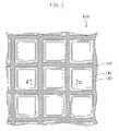
- FIG. 1is a schematic plan view illustrating an organic EL element 100 of Embodiment 1.
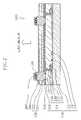
- FIG. 2is a schematic sectional view taken along the line II-II shown in FIG. 1 .
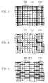
- FIG. 3is a schematic plan view illustrating an example of the arrangement of an auxiliary electrode 150 .
- FIG. 4is a schematic plan view illustrating an example of the arrangement of the auxiliary electrode 150 .
- FIG. 5is a schematic plan view illustrating an example of the arrangement of the auxiliary electrode 150 .
- FIG. 6is a schematic sectional view of the organic EL element 100 in which the auxiliary electrode 150 is formed on part of a wall-like insulating layer 140 which defines pixels from each other.
- FIG. 7is a schematic sectional view of the organic EL element 100 in which the auxiliary electrode 150 is formed on part 140 a of the wall-like insulating layer 140 positioned between an organic light emitting layer 130 G and an organic light emitting layer 130 R.
- FIG. 8is a flowchart illustrating some of the steps of manufacturing the organic EL element 100 .
- FIG. 9is a schematic diagram of an organic EL display device D including the organic EL element 100 .
- FIG. 10is a plan view illustrating an organic EL element 200 of Embodiment 2.
- FIG. 11is a plan view illustrating an organic EL element 300 of Embodiment 3.
- FIG. 12is a plan view illustrating an organic EL element 400 of Embodiment 4.
- FIG. 13is a schematic sectional view of an organic EL element 500 of Embodiment 5.
- FIG. 14is a schematic sectional view of a conventional organic EL element 600 .
- FIG. 1is a schematic plan view illustrating an organic EL element 100 of Embodiment 1.
- FIG. 2is a schematic sectional view taken along the line II-II shown in FIG. 1 .
- the organic EL element 100includes a thin film transistor (TFT) substrate 110 , a plurality of first electrodes 120 which are arranged on the TFT substrate 110 in a predetermined configuration (e.g., a matrix configuration), a wall-like insulating layer 140 which isolates the first electrodes 120 from each other, organic light emitting layers 130 formed on the first electrodes 120 , respectively, an auxiliary electrode 150 formed on the wall-like insulating layer 140 and a second electrode 160 which is formed to cover the surfaces of the wall-like insulating layer 140 , the auxiliary electrode 150 and the organic light emitting layers 130 and electrically connected to the auxiliary electrode 150 .
- the second electrode 160is transparent to light emitted from the organic light emitting layer 130 . For the convenience' sake, the second electrode 160 is omitted from FIG. 1 .
- the TFT substrate 110includes an insulating substrate 111 , a plurality of TFTs 114 connected to the respective first electrodes 120 arranged in the predetermined configuration, source electrodes 112 and gate electrodes 113 which are electrically connected to the TFTs 114 and a planarization film 115 for planarizing one of the surfaces of the TFT substrate 110 above which the organic light emitting layers 130 are formed.
- the insulating substrate 111is preferably made of insulating material which ensures the mechanical strength of the organic EL element 100 .
- the insulating substrate 111may be made of quartz, glass such as soda glass, inorganic material such as ceramic or organic material such as polyimide and polyester.
- Each of the TFTs 114is formed of a gate electrode 113 , a gate insulating film 117 formed on the gate electrode 113 , an island-shaped semiconductor 118 which is insulated from the gate electrode 113 by the gate insulating film 117 and a TFT electrode 119 which is formed to cover the peripheral portion of the island-shaped semiconductor 118 (bottom gate TFTs).
- the TFTsare not limited to bottom gate TFTs.
- the TFTsmay be top gate TFTs.
- the first electrodes 120are arranged on the TFT substrate 110 in a predetermined configuration (e.g., a matrix configuration). Each of the first electrodes 120 is connected to the TFT electrode 119 via a connection part (through hole) 121 formed in the planarization film 115 . The first electrodes 120 implant holes into the organic light emitting layers 130 in response to signals input from the TFTs 114 .
- the first electrodes 120are preferably arranged not to overlap the gate electrodes 113 or the source electrodes 112 . If the first electrodes 120 overlap the source electrodes 112 or the gate electrodes 113 , a high parasitic resistance is generated to deteriorate display quality.
- Examples of material for the first electrodes 120include metal material such as silver (Ag) and aluminum (Al) and conductive oxides such as indium tin oxide (ITO) and indium zinc oxide (IZO).
- metal materialsuch as silver (Ag) and aluminum (Al)
- conductive oxidessuch as indium tin oxide (ITO) and indium zinc oxide (IZO).
- the first electrodes 120are preferably made of material having a high work function such as indium tin oxide (ITO). Further, in the organic EL element 100 , light emitted by the light emitting layers 130 is output through the second electrode 160 . Therefore, it is preferred that the first electrodes 120 are light-reflective. That is, the first electrodes 120 are preferably made of light reflective material such as silver (Ag) or aluminum (Al).
- the first electrodes 120may have a multilayer structure of a metal layer made of aluminum (Al) having high conductivity and high light reflectance and an electrode layer made of indium zinc oxide (IZO) having a high work function. By so doing, the first electrodes 120 are given with both high light reflectance and high hole implantation efficiency. This allows providing the organic EL element 100 with higher luminance.
- Alaluminum
- IZOindium zinc oxide
- Each of the first electrodes 120 in the organic EL element 100 of Embodiment 1is rectangular. However, the shape of the first electrodes 120 may be varied (e.g., they may be round, oval or the like).
- the surfaces of the first electrodes 120are preferably subjected to a UV/O 3 treatment to render the surfaces nonrepellent to the solvent (ink).
- the first electrodes 120improve in affinity for ink for forming the organic light emitting layers 130 . Accordingly, the organic light emitting layers 130 are formed more uniformly. As a result, the organic EL element 100 is obtained with fewer defects.
- the wall-like insulating layer 140is grid-shaped when viewed in plan so that it isolates the first electrodes 120 arranged in the predetermined configuration (matrix configuration) from each other.
- the wall-like insulating layer 140is preferably made of material which is less likely to become deformed or vary in property upon heating.
- the wall-like insulating layer 140may be made of photosensitive polyimide, an acrylic resin, a methacrylate resin or a novolac resin.
- Preferable material for the wall-like insulating layer 140is a photosensitive resin because it allows patterning of the wall-like insulating layer 140 by photolithography. That is, the wall-like insulating layer 140 is patterned easily into the grid shape without etching or peeling.
- the wall-like insulating layer 140is preferably made of material which is repellent to an organic solvent (ink) (hereinafter this property is referred to as liquid repellency).
- inkorganic solvent
- the liquid-repellant wall-like insulating layer 140may be made of organic material such as polyimide or an acrylic resin doped with a fluorine or silicon-based additive.
- the liquid repellencymay be added to the wall-like insulating layer 140 after the formation thereof.
- the liquid repellencymay be added thereto by a treatment with oxygen plasma or tetrafluorocarbon plasma.
- the organic light emitting layers 130are formed on the first electrodes 120 which are isolated by the grid-shaped wall-like insulating layer 140 from each other.
- Each of the organic light emitting layers 130includes a hole transport layer 131 and a light emitting layer 132 .
- the organic light emitting layer 130may be formed of the light emitting layer 132 only.
- the organic light emitting layer 130may be formed of the light emitting layer 132 and one or more layers of a hole implantation layer, the hole transport layer 131 , an electron transport layer and an electron implantation layer.
- the hole transport layer 131transports holes implanted from the first electrode 120 to the light emitting layer 132 .
- the hole transport layer 131preferably has high hole transport efficiency.
- suitable material for forming the hole transport layer 131 of high transport efficiencyinclude low molecular materials such as a porphyrin compound, an aromatic tertiary amine compound, a hydrazone compound, a quinacridon compound and a stilamine compound.
- examples of the aromatic tertiary amine compoundinclude N,N′-bis-(3-methylphenyl)-N,N′-bis-(phenyl)-benzidine (TPD) and N,N′-di(naphthalene-1-il)-N,N′-diphenyl-benzidine (NPD).
- TPDN,N′-bis-(3-methylphenyl)-N,N′-bis-(phenyl)-benzidine
- NPDN,N′-di(naphthalene-1-il)-N,N′-diphenyl-benzidine
- high molecular material suitable for forming the hole transport layer 131examples include polyaniline, 3,4-polyethylenedioxythiophene/polystyrenesulphonate (PEDT/PSS), poly(triphenylamine) derivatives and polyvinylcarbazole (PVCz). Further, examples of precursors of high molecular material suitable for forming the hole transport layer 131 include a poly(p-phenylene vinylene) precursor and a poly(p-naphthalene vinylene) precursor.
- the hole transport layer 131is not limited to a single-layered one and may have a multilayer structure. Further, a hole implantation layer may be provided between the hole transport layer 131 and the light emitting layer 132 . With the hole implantation layer interposed therebetween, hole implantation to the light emitting layer 132 is performed with improved efficiency. This allows providing the organic EL element 100 with higher luminance.
- Holes implanted from the first electrode 120 and electrons implanted from the second electrode 160are recombined in the light emitting layer 132 to generate excitons in the light emitting layer 132 .
- the excitonsare deactivated to enter the ground state, light is emitted from the light emitting layer 132 .
- the light emitting layer 132may contain low molecular light emitting material or high molecular light emitting material.
- the light emitting layer 132 containing the low molecular light emitting materialmay be formed by vacuum deposition.
- the light emitting layer 132 containing the high molecular light emitting materialmay be formed by the wet application process such as inkjet printing or spin coating. According to the wet application process, the organic EL element 100 including the high-definition, large-area TFT substrate 110 is manufactured by fewer steps at low costs.
- Examples of material for the light emitting layer 132include: poly(2-decyloxy-1,4-phenylene) (DO-PPP); poly[2,5-bis-[2-(N,N,N-triethylammonium) ethoxy]-1,4-phenyl-alto-1,4-phenylene]dibromide (PPP-Net 3+ ); and poly[2-(2′-ethylhexyloxy)-5-methoxy-1,4-phenylenevinylene] (MEH-PPV).
- DO-PPPpoly(2-decyloxy-1,4-phenylene)
- PPP-Net 3+poly[2,5-bis-[2-(N,N,N-triethylammonium) ethoxy]-1,4-phenyl-alto-1,4-phenylene]dibromide
- MEH-PPVpoly[2-(2′-ethylhexyloxy)-5-methoxy-1,4-
- the second electrode 160is formed as a layer which covers the surfaces of the auxiliary electrode 150 , the organic light emitting layers 130 and the wall-like insulating layer 140 .
- the second electrode 160implants electrons into the organic light emitting layers 130 .
- the second electrode 160preferably has high light transmittance so that light from the light emitting layer 132 is passed therethrough.
- the second electrode 160may suitably be made of indium tin oxide (ITO) or indium zinc oxide (IZO).
- the second electrode 160is preferably made of material having a low work function. Examples of such material include calcium (Ca) and aluminum (Al).
- the second electrode 160may have a layered structure of a metal layer made of calcium (Ca) or aluminum (Al) having a low work function and a transparent electrode layer made of indium tin oxide (ITO) or the like having high light transmittance. By so doing, the second electrode 160 is given with both high electron implantation efficiency and high light transmittance. This allows providing the organic EL element 100 with higher luminance.
- the second electrode 160may be made of an ultra-thin film made of metal or the like.
- the second electrode 160is formed as a single layer covering the surfaces of the organic light emitting layers 130 , but the second electrode 160 may be divided into two or more electrode layers.
- the second electrode 160is electrically connected to the auxiliary electrode 150 formed below the second electrode 160 . Since the auxiliary electrode 150 is lower than the second electrode 160 in electric resistance, the auxiliary electrode 150 reduces the surface resistance of the second electrode 160 . Therefore, the occurrence of unevenness in image display, which is caused by a drop in voltage in the second electrode 160 , is prevented effectively, whereby uniform image display is realized by the organic EL element 100 . Further, since the auxiliary electrode 150 reduces the surface resistance of the second electrode 160 , the organic EL element 100 can be driven at a low voltage.
- the auxiliary electrode 150may be made of low resistance metal material. Examples of such material include copper (Cu), tantalum (Ta), titanium (Ti), chromium (Cr), aluminum (Al) and silver (Ag).
- the auxiliary electrode 150 of Embodiment 1is formed on the entire wall-like insulating layer 140 having a grid-like plane configuration.
- the present inventionis not limited thereto.
- FIGS. 3 to 5are schematic plan views illustrating how the auxiliary electrode 150 is formed.
- the auxiliary electrode 150may be formed on top of part of the wall-like insulating layer 140 .
- the auxiliary electrode 150may be divided into multiple fragmentary electrodes. Any of the arrangements shown in FIGS. 3 to 5 allows reduction in surface resistance of the second electrode 160 . Therefore, a drop in voltage in the second electrode 160 is prevented from occurring.
- the other part of the wall-like insulating layer 140 on top of which the auxiliary electrode 150 is not formedmay be smaller in width than the part thereof on top of which the auxiliary electrode 150 is formed. That is, the part of the wall-like insulating layer 140 on top of which the auxiliary electrode 150 is formed may be wider than the part thereof on top of which the auxiliary electrode 150 is not formed.
- the area ratio of the wall-like insulating layer 140 to the display regioni.e., the area ratio of a non-emission region, is reduced.
- the organic EL element 100is provided with higher luminance and higher aperture ratio.
- the part of the wall-like insulating layer 140 on top of which the auxiliary electrode 150 is formedare preferably about twice or more wider than the other part of the wall-like insulating layer 140 .
- the wall-like insulating layer 140prevents the mixing of the organic light emitting layers 130 .
- the width of the grid lines forming the wall-like insulating layer 140is minimized to such a degree that even if the ink droplet is misaligned with the intended position, the ink droplet does not reach the adjacent organic light emitting layer 130 .
- the part of the wall-like insulating layer 140 on top of which the auxiliary electrode 150 is formedis designed to have a width twice or more larger than the minimum width.
- the organic EL element 100is a full-color organic EL element including subpixels for emitting red (R) light, green (G) light and blue (B) light
- the auxiliary electrode 150may be formed only on some of the grid lines of the wall-like insulating layer 140 which define pixels, each including a set of a subpixel for emitting red light, a subpixel for emitting green light and a subpixel for emitting blue light, from each other.
- the pixelincludes two or more subpixels.
- the pixelis not limited to the one including three subpixels for emitting lights of different colors.
- the two or more subpixels for a single pixelmay emit lights of the same color.
- the two or more subpixels for a single pixelmay emit lights of different colors.
- a single pixelmay include four subpixels for emitting lights of red (R), green (G), blue (B) and white (W), respectively.
- the subpixelsare formed of the organic light emitting layers 130 , respectively.
- FIG. 6is a schematic sectional view of the organic EL element 100 in which the auxiliary electrode 150 is formed on the some of the grid lines of the wall-like insulating layer 140 which define the pixels from each other.
- each of the pixelsincludes an organic light emitting layer 130 R for emitting red light, an organic light emitting layer 130 G for emitting green light and an organic light emitting layer 130 B for emitting blue light.
- the auxiliary electrode 150is formed only on the some of the grid lines of the wall-like insulating layer 140 which define the pixels from each other, i.e., on the grid lines 140 a of the wall-like insulating layer 140 , each of which is positioned between the organic light emitting layer 130 R and the organic light emitting layer 130 B.
- the auxiliary electrode 150is not formed on the grid lines 140 b of the wall-like insulating layer 140 , each of which is positioned between the organic light emitting layer 130 R and the organic light emitting layer 130 G, and the grid lines 140 b of the wall-like insulating layer 140 , each of which is positioned between the organic light emitting layer 130 G and the organic light emitting layer 130 B. If the auxiliary electrode 150 is formed on every grid line of the wall-like insulating layer 140 , limitations are often imposed by the manufacturing process and every grid line of the wall-like insulating layer 140 must have a larger width as compared with the case where the auxiliary electrode 150 is formed on some of the grid lines. This may lead to a decrease in light emitting area par pixel.
- the decrease in light emitting area par pixelis minimized as possible. Therefore, the resulting organic EL element 100 is provided with higher luminance.
- the structure shown in FIG. 6is also effective in reducing the surface resistance of the second electrode 160 .
- the auxiliary electrode 150may be formed on some of the grid lines of the wall-like insulating layer 140 which are adjacent to the light emitting layers 130 having the smallest light emitting area. More specifically, the auxiliary electrode 150 may be formed on some of the grid lines of the wall-like insulating layer 140 positioned between the organic light emitting layers 130 G and the organic light emitting layers 130 R. In consideration of mutual relationship among light emission efficiency, chromaticity and life, the organic light emitting layers 130 G are given with the smallest light emitting area, while the organic light emitting layer 130 R are given with the second smallest area.
- FIG. 7is a schematic sectional view of the organic EL element 100 in which the auxiliary electrode 150 is formed on the grid lines 140 a of the wall-like insulating layer 140 , each of which is positioned between the organic light emitting layer 130 G and the organic light emitting layer 130 R.
- material for emitting green lightshows the highest luminance
- material for emitting red lightshows the lowest luminance
- the luminance of material for emitting blue lightlies between that of the material for emitting green light and that of the material for emitting red light. Therefore, if the organic EL element includes the organic light emitting layers 130 R containing the material for red light emission, the organic light emitting layers 130 G for green light emission and the organic light emitting layers 130 B for blue light emission, and the organic light emitting layers 130 R, 130 G and 130 B have the same light emitting area, electric current applied to the organic light emitting layers 130 R needs to be higher than those applied to the organic light emitting layers 130 G and 130 B to equalize the luminance of the organic light emitting layers 130 R, 130 G and 130 B. However, since the luminance of the organic light emitting layers 130 B is attenuated at the highest rate, color balance is varied over time and color drift occurs in a displayed image.
- the organic light emitting layers 130 Bare given with the largest light emitting area and the organic light emitting layers 130 G are given with the smallest light emitting area, the deterioration of the organic light emitting layers 130 B is slowed relative to the organic light emitting layers 130 R and 130 G. That is, the luminance attenuation rates of the organic light emitting layers 130 R, 130 G and 130 B are substantially equalized. As a result, color balance of a displayed image is less likely to vary over time and the organic EL element 100 is provided with long life.
- the organic light emitting layer 130 Bis given with the largest light emitting area and the organic light emitting layer 130 G is given with the smallest light emitting area, a non-emission region between the organic light emitting layer 130 G of the smallest area and the organic light emitting layer 130 R may become relatively wide due to limitations on design of the TFT substrate 110 . Therefore, if the wall-like insulating layer 140 is formed in the wide non-emission region between the organic light emitting layers 130 G and 130 R and the auxiliary electrode 150 is formed thereon, the aperture ratio is hardly sacrificed by the formation of the auxiliary electrode 150 .
- the organic EL element 100is provided with high luminance, long life and high aperture ratio, while color balance of a displayed image is less likely to vary over time.
- FIG. 8is a flowchart illustrating some of the steps of manufacturing the organic EL element 100 .
- a source electrodes 112 , gate electrodes 113 , TFTs 114 and planarization film 115are formed on an insulating substrate 111 .
- a film of conductive materialsuch as aluminum (Al) is formed by sputtering. The thus formed conductive film is patterned into a desired shape to obtain first electrodes 120 (S 1 ).
- organic light emitting layers 130are formed by a wet application process (inkjet printing, spin coating or the like) in a later step, the surfaces of the first electrodes 120 are subjected to a UV/O 3 treatment to give them an affinity for liquid (to render the surfaces nonrepellent to an organic solvent used for inkjet printing) (S 2 ). Rendering the surfaces of the first electrodes 120 nonrepellent to liquid, an affinity between the first electrodes 120 and the organic light emitting layers 130 improves. As a result, the organic light emitting layers 130 are formed more uniformly. Thus, an organic EL element 100 is obtained with fewer defects.
- a wall-like insulating layer 140is formed (S 3 ).
- the wall-like insulating layer 140may be formed by the following method. First, a thin film of photosensitive polyimide or the like is formed by spin coating. Then, the obtained thin polyimide film is patterned into a desired shape by a photoresist process including photoresist application, pre-baking, light exposure, development, post-baking, etching and photoresist peeling. Thus, the wall-like insulating layer 140 is obtained.
- the wall-like insulating layer 140is preferably made of liquid-repellant material doped with a fluorine or silicon-based additive.
- the surface of the wall-like insulating layer 140may be subjected to such a treatment that gives liquid repellency (a property of rejecting liquid (ink) containing material for forming the organic light emitting layers 130 ).
- the treatment for giving liquid repellencymay be performed using oxygen plasma or tetrafluorocarbon plasma. Giving liquid repellency to the surface of the wall-like insulating layer 140 effectively prevents ink droplets containing the material for forming the organic light emitting layers 130 from misalignment with the intended positions.
- an auxiliary electrode 150is formed on the wall-like insulating layer 140 .
- the auxiliary electrode 150may be formed by sputtering, for example.
- a hole transport layer 131 and a light emitting layer 132are formed by the wet application process (inkjet printing, spin coating or the like) to obtain the organic light emitting layer 130 .
- the wet application processsuch as inkjet printing or spin coating, the organic light emitting layers 130 are formed at low costs by relatively few manufacturing steps.
- ink containing the material for forming the organic light emitting layers 130is applied (S 4 ) and the applied ink is dried (S 5 ).
- steps of forming the organic light emitting layers 130are explained in detail.
- ink containing material for forming the hole transport layers 131is applied onto the first electrodes 120 (S 4 ).
- the applied inkis dried to obtain the hole transport layers 131 (S 5 ).
- ink containing material for the light emitting layers 132is applied to the hole transport layers 131 (S 4 ) and the applied ink is dried to obtain the light emitting layers 132 (S 5 ).
- a second electrode 160is formed to cover the surfaces of the organic light emitting layers 130 .
- the second electrode 160may be formed by sputtering.
- FIG. 9is a schematic diagram of an organic EL display device D including the organic EL element 100 .
- the organic EL element 100allows image display with high luminance and reduced variations in luminance and is manufactured by fewer manufacturing steps at low costs. Therefore, the organic EL display device D including the organic EL element 100 is also capable of displaying images with high luminance and reduced variations in luminance and manufactured by fewer manufacturing steps at low costs.
- An organic EL element 200 of Embodiment 2is substantially the same as the organic EL element 100 of Embodiment 1 except where to provide the auxiliary electrode and the structure of the pixels. Now, with reference to the drawings, a detailed explanation is given of where to provide the auxiliary electrode and the structure of pixels P in the organic EL element 200 of Embodiment 2.
- FIG. 10is a plan view illustrating the organic EL element 200 of Embodiment 2.
- the organic EL element 200includes organic light emitting layers 230 B for emitting blue (B) light, organic light emitting layers 230 R for emitting red (R) light and organic light emitting layers 230 G for emitting green (G) light.
- organic light emitting layers 230 B, 230 R and 230 Gthe organic light emitting layers 230 B have the largest light emitting area, while the organic light emitting layers 230 G have the smallest light emitting area.
- the light emitting area of the organic light emitting layers 230 Ris smaller than that of the organic light emitting layers 230 B and larger than that of organic light emitting layers 230 G.
- green light emitting materialshows the highest light emission efficiency and red light emitting material shows the lowest luminance. Further, the luminance of the organic light emitting layers 230 B is attenuated at the highest rate. Therefore, color balance is varied over time, causing color drift in a displayed image.
- the light emitting areas of the organic light emitting layers 230 B, 230 R and 230 Gare varied in consideration of the differences in duration of light emission of the organic light emitting layers 230 B, 230 R and 230 G (luminance attenuation rate) and light emission efficiency. Therefore, the organic EL element 200 is provided with long life while variations in color balance over time are reduced.
- the organic light emitting layers 230 Bare given with the largest light emitting area and the organic light emitting layers 230 G are given with the smallest light emitting area.
- the organic EL element 200includes pixels P, each of which includes an organic light emitting layer 230 B, an organic light emitting layer 230 R and an organic light emitting layer 230 G.
- the organic light emitting layer 230 Bis adjacent to the organic light emitting layers 230 R and 230 G
- the organic light emitting layer 230 Gis adjacent to the organic light emitting layers 230 R and 230 B.
- the organic light emitting layers 230 B, 230 R and 230 Gare arranged in an almost delta configuration.
- the “almost delta configuration”indicates that three light emitting regions in a single pixel are so arranged that the centers of gravity thereof form a triangle.
- a relatively wide spacemay be generated in the vicinity of the organic light emitting layer 230 G having the smallest light emitting area. More specifically, the relatively wide space may be generated between the organic light emitting layer 230 B and the organic light emitting layers 230 R and 230 G.
- part of the wall-like insulating layer 140 present at the wide space in the pixelsis given with a relatively larger width than the other part.
- an auxiliary electrode 250is formed on the relatively wider part of the wall-like insulating layer 140 . By so doing, the aperture ratio is hardly reduced by the formation of the auxiliary electrode 250 .
- the organic EL element 200is provided with high luminance and reduced variations in luminance.
- An organic EL element 300 of Embodiment 3is substantially the same as the organic EL element 100 of Embodiment 1 except where to provide the auxiliary electrode and the structure of the pixels. Now, with reference to the drawings, a detailed explanation is given of where to provide the auxiliary electrode and the structure of pixels P in the organic EL element 300 of Embodiment 3.
- FIG. 11is a plan view illustrating the organic EL element 300 of Embodiment 3.
- the organic EL element 300includes organic light emitting layers 330 B for emitting blue light, organic light emitting layers 330 R for emitting red light and organic light emitting layers 330 G for emitting green light.
- the organic light emitting layers 330 B, 330 R and 330 Ghave the largest light emitting area, while the organic light emitting layers 330 G have the smallest light emitting area.
- the light emitting area of the organic light emitting layers 330 Ris smaller than that of the organic light emitting layers 330 B and larger than that of organic light emitting layers 330 G. Therefore, the organic EL element 300 of Embodiment 3 does not show significant variations in color balance over time and offers long life.
- the organic EL element 300includes pixels P, each of which includes an organic light emitting layer 330 B, an organic light emitting layer 330 R and an organic light emitting layer 330 G.
- the organic light emitting layers 330 B, 330 R and 330 Gare arranged in the almost delta configuration.
- the organic EL element 300 shown in FIG. 11due to limitations on the design of the TFT substrate (especially, the positions of through holes), a relatively wide space may be generated in the vicinity of the organic light emitting layer 330 G having the smallest light emitting area.
- an auxiliary electrode 350is formed in space between the organic light emitting layers 330 G and 330 R and between the organic light emitting layers 330 G and 330 B. By so doing, the aperture ratio is hardly reduced by the formation of the auxiliary electrode 350 .
- the organic EL element 300is provided with high luminance and reduced variations in luminance.
- the auxiliary electrode 350is divided into multiple electrodes formed one by one in every pixel P. Also in this case, the surface resistance of the second electrode (shared upper electrode) is effectively reduced.
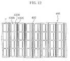
- An organic EL element 400 of Embodiment 4is substantially the same as the organic EL element 1 of Embodiment 1 except where to provide the auxiliary electrode and the structure of the pixels. Now, with reference to the drawings, a detailed explanation is given of where to provide the auxiliary electrode and the structure of pixels in the organic EL element 400 of Embodiment 3.
- FIG. 12is a plan view illustrating the organic EL element 400 of Embodiment 3.
- the organic EL element 400includes organic light emitting layers 430 B for emitting blue light, organic light emitting layers 430 R for emitting red light and organic light emitting layers 430 G for emitting green light.
- the organic light emitting layers 430 B, 430 R and 430 Ghave the largest light emitting area, while the organic light emitting layers 430 G have the smallest light emitting area.
- the light emitting area of the organic light emitting layers 430 Ris smaller than that of the organic light emitting layers 430 B and larger than that of organic light emitting layers 430 G. Therefore, the organic EL element 400 of Embodiment 3 does not show significant variations in color balance over time and offers long life.
- the organic EL element 400includes pixels P, each of which includes an organic light emitting layer 430 B, an organic light emitting layer 430 R and an organic light emitting layer 430 G.
- the organic light emitting layers 430 B, 430 R and 430 Gare arranged in a stripe configuration. More specifically, the organic light emitting layers 430 B, 430 R and 430 G, each of which is in the form of an elongated rectangle, are arranged parallel to each other.
- a relatively wide spacemay be generated in the vicinity of the organic light emitting layer 430 G having the smallest light emitting area. More specifically, the relatively wide space may be generated between the organic light emitting layer 430 G and the organic light emitting layer 430 R.
- some of the grid lines of the wall-like insulating layer 140 positioned at the wide spaceare given with a relatively larger width than the other grid lines.
- an auxiliary electrode 450is formed on the relatively wider part of the wall-like insulating layer 140 . By so doing, the aperture ratio is hardly reduced by the formation of the auxiliary electrode 450 .
- the organic EL element 400is provided with high luminance and reduced variations in luminance.
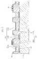
- FIG. 13is a schematic sectional view of an organic EL element 500 of Embodiment 5.
- the organic EL element 500 of Embodiment 5is substantially the same as the organic EL element 100 of Embodiment 1 except that a liquid repellent layer is further provided between the auxiliary electrode 150 and the second electrode 160 .
- the organic EL element 500includes a TFT substrate 510 , a plurality of first electrodes 520 arranged in a predetermined configuration (e.g., matrix configuration), a wall-like insulating layer 540 which isolates the first electrodes 520 from each other, organic light emitting layers 530 formed on the first electrodes 520 , respectively, an auxiliary electrode 500 formed on the wall-like insulating layer 540 , a liquid repellent layer 570 which covers the auxiliary electrode 550 and a second electrode 560 which is formed to cover the surfaces of the water repellent layer 570 , wall-like insulating layer 540 and auxiliary electrode 550 and electrically connected to the auxiliary electrode 550 via through holes 571 .
- Each of the organic light emitting layers 530includes a hole transport layer 531 and a light emitting layer 532 .
- the second electrode 560is transparent to light emitted from the light emitting layer 532 .
- the TFT substrate 510includes an insulating substrate 511 , TFTs 514 which are connected to the first electrodes 520 , respectively, source electrodes 512 and gate electrodes 513 which are electrically connected to the TFTs 514 , respectively, and a planarization film 515 for planarizing one of the surfaces of the TFT substrate 510 facing the organic light emitting layers 530 .
- the liquid repellent layer 570has liquid repellency. Therefore, even if ink droplets which are ejected to form the organic light emitting layers 530 by inkjet printing reach the surface of the liquid repellent layer 570 , the ink droplets slide down to the desired positions. Thus, the ink droplets are prevented from remaining on the liquid repellent layer 570 . In this way, the electrical connection between the auxiliary electrode 500 and the second electrode 560 is ensured.
- the liquid repellent layer 570may be made of a polyimide resin doped with a fluorine or silicon-based additive.
- the liquid repellent layer 570may also be provided by forming a film which is not liquid-repellent and giving the film liquid repellency by a certain treatment.
- the treatmentinclude a treatment with oxygen plasma or tetrafluorocarbon plasma. Oxygen plasma and tetrafluorocarbon plasma may be used in combination.
- the previously formed auxiliary electrode 550may be subjected to the oxygen plasma treatment or the tetrafluorocarbon plasma treatment to form the liquid repellent layer 570 at the top surface of the auxiliary electrode 550 .
- the liquid repellent layer 570may be a monolayer.
- the monolayeris extremely thin and has electric conductivity. Therefore, if the liquid repellent layer 570 is a monolayer, the auxiliary electrode 550 and the second electrode 560 are electrically connected without forming the through hole 571 in the liquid repellent layer 570 . By so doing, the organic EL element 500 is manufactured more easily.
- the monolayermay be made of stearic acid.
Landscapes
- Engineering & Computer Science (AREA)
- Microelectronics & Electronic Packaging (AREA)
- Physics & Mathematics (AREA)
- Optics & Photonics (AREA)
- Manufacturing & Machinery (AREA)
- Electroluminescent Light Sources (AREA)
- Devices For Indicating Variable Information By Combining Individual Elements (AREA)
Abstract
Description
Claims (14)
Applications Claiming Priority (4)
| Application Number | Priority Date | Filing Date | Title |
|---|---|---|---|
| JP2004214491 | 2004-07-22 | ||
| JP2004-214491 | 2004-07-22 | ||
| JP2005-092088 | 2005-03-28 | ||
| JP2005092088AJP4121514B2 (en) | 2004-07-22 | 2005-03-28 | ORGANIC LIGHT EMITTING ELEMENT AND DISPLAY DEVICE INCLUDING THE SAME |
Publications (2)
| Publication Number | Publication Date |
|---|---|
| US20060017375A1 US20060017375A1 (en) | 2006-01-26 |
| US7495389B2true US7495389B2 (en) | 2009-02-24 |
Family
ID=35656412
Family Applications (1)
| Application Number | Title | Priority Date | Filing Date |
|---|---|---|---|
| US11/157,889Active2027-02-14US7495389B2 (en) | 2004-07-22 | 2005-06-21 | Organic light emitting element including auxiliary electrode, display device including the same and method for manufacturing the organic light emitting element |
Country Status (3)
| Country | Link |
|---|---|
| US (1) | US7495389B2 (en) |
| JP (1) | JP4121514B2 (en) |
| KR (1) | KR100669265B1 (en) |
Cited By (56)
| Publication number | Priority date | Publication date | Assignee | Title |
|---|---|---|---|---|
| US20060055999A1 (en)* | 2004-08-26 | 2006-03-16 | Lg Philips Lcd Co., Ltd. | Organic electro luminescence device and fabrication method thereof |
| US20080185959A1 (en)* | 2007-02-06 | 2008-08-07 | Seiko Epson Corporation | Organic el device, method for producing organic el device, and electronic apparatus |
| US20080284323A1 (en)* | 2007-05-14 | 2008-11-20 | Sony Corporation | Organic electroluminescence display device |
| US20090135103A1 (en)* | 2007-11-27 | 2009-05-28 | Changnam Kim | Organic light emitting device |
| US20100156273A1 (en)* | 2008-12-24 | 2010-06-24 | Seiko Epson Corporation | Electroluminescence apparatus, method for manufacturing electroluminescence apparatus, and electronic appartus |
| US20130299812A1 (en)* | 2011-01-25 | 2013-11-14 | Idemitsu Kosan Co., Ltd | Organic electroluminescent element and illumination device |
| US20140246664A1 (en)* | 2011-10-18 | 2014-09-04 | Toppan Printing Co., Ltd. | Organic electroluminescence display panel and manufacturing method therefor |
| US8852687B2 (en) | 2010-12-13 | 2014-10-07 | Samsung Display Co., Ltd. | Organic layer deposition apparatus |
| US8859043B2 (en) | 2011-05-25 | 2014-10-14 | Samsung Display Co., Ltd. | Organic layer deposition apparatus and method of manufacturing organic light-emitting display device by using the same |
| US8859325B2 (en) | 2010-01-14 | 2014-10-14 | Samsung Display Co., Ltd. | Thin film deposition apparatus, method of manufacturing organic light-emitting display device by using the apparatus, and organic light-emitting display device manufactured by using the method |
| US8865252B2 (en) | 2010-04-06 | 2014-10-21 | Samsung Display Co., Ltd. | Thin film deposition apparatus and method of manufacturing organic light-emitting display device by using the same |
| US8871542B2 (en) | 2010-10-22 | 2014-10-28 | Samsung Display Co., Ltd. | Method of manufacturing organic light emitting display apparatus, and organic light emitting display apparatus manufactured by using the method |
| US8876975B2 (en) | 2009-10-19 | 2014-11-04 | Samsung Display Co., Ltd. | Thin film deposition apparatus |
| US8882922B2 (en) | 2010-11-01 | 2014-11-11 | Samsung Display Co., Ltd. | Organic layer deposition apparatus |
| US8882556B2 (en) | 2010-02-01 | 2014-11-11 | Samsung Display Co., Ltd. | Thin film deposition apparatus, method of manufacturing organic light-emitting display device by using the apparatus, and organic light-emitting display device manufactured by using the method |
| US8894458B2 (en) | 2010-04-28 | 2014-11-25 | Samsung Display Co., Ltd. | Thin film deposition apparatus, method of manufacturing organic light-emitting display device by using the apparatus, and organic light-emitting display device manufactured by using the method |
| US8906731B2 (en) | 2011-05-27 | 2014-12-09 | Samsung Display Co., Ltd. | Patterning slit sheet assembly, organic layer deposition apparatus, method of manufacturing organic light-emitting display apparatus, and the organic light-emitting display apparatus |
| US8951610B2 (en) | 2011-07-04 | 2015-02-10 | Samsung Display Co., Ltd. | Organic layer deposition apparatus |
| US8956697B2 (en) | 2012-07-10 | 2015-02-17 | Samsung Display Co., Ltd. | Method of manufacturing organic light-emitting display apparatus and organic light-emitting display apparatus manufactured by using the method |
| US8968829B2 (en) | 2009-08-25 | 2015-03-03 | Samsung Display Co., Ltd. | Thin film deposition apparatus and method of manufacturing organic light-emitting display device by using the same |
| US8973525B2 (en) | 2010-03-11 | 2015-03-10 | Samsung Display Co., Ltd. | Thin film deposition apparatus |
| US9024306B2 (en) | 2011-05-20 | 2015-05-05 | Panasonic Intellectual Property Management Co., Ltd. | Organic electroluminescence element |
| US9165996B2 (en) | 2012-10-19 | 2015-10-20 | Samsung Display Co., Ltd. | Organic light emitting display device and manufacturing method thereof |
| US9214494B2 (en)* | 2012-12-10 | 2015-12-15 | LuxVue Technology Corporation | Active matrix display panel with ground tie lines |
| US9249493B2 (en) | 2011-05-25 | 2016-02-02 | Samsung Display Co., Ltd. | Organic layer deposition apparatus and method of manufacturing organic light-emitting display apparatus by using the same |
| US9279177B2 (en) | 2010-07-07 | 2016-03-08 | Samsung Display Co., Ltd. | Thin film deposition apparatus, method of manufacturing organic light-emitting display device by using the apparatus, and organic light-emitting display device manufactured by using the method |
| US9306191B2 (en) | 2012-10-22 | 2016-04-05 | Samsung Display Co., Ltd. | Organic light-emitting display apparatus and method of manufacturing the same |
| US9343448B2 (en) | 2012-12-10 | 2016-05-17 | LuxVue Technology Corporation | Active matrix emissive micro LED display |
| US9388488B2 (en) | 2010-10-22 | 2016-07-12 | Samsung Display Co., Ltd. | Organic film deposition apparatus and method of manufacturing organic light-emitting display device by using the same |
| US9450140B2 (en) | 2009-08-27 | 2016-09-20 | Samsung Display Co., Ltd. | Thin film deposition apparatus and method of manufacturing organic light-emitting display apparatus using the same |
| US9461277B2 (en) | 2012-07-10 | 2016-10-04 | Samsung Display Co., Ltd. | Organic light emitting display apparatus |
| US9466647B2 (en) | 2012-07-16 | 2016-10-11 | Samsung Display Co., Ltd. | Flat panel display device and method of manufacturing the same |
| US9620487B2 (en) | 2012-12-10 | 2017-04-11 | Apple Inc. | Light emitting device reflective bank structure |
| US9680123B2 (en) | 2014-12-11 | 2017-06-13 | Industrial Technology Research Institute | Light emitting device, electrode structure and manufacturing method thereof |
| US9748483B2 (en) | 2011-01-12 | 2017-08-29 | Samsung Display Co., Ltd. | Deposition source and organic layer deposition apparatus including the same |
| US10246769B2 (en) | 2010-01-11 | 2019-04-02 | Samsung Display Co., Ltd. | Thin film deposition apparatus |
| US10270033B2 (en) | 2015-10-26 | 2019-04-23 | Oti Lumionics Inc. | Method for patterning a coating on a surface and device including a patterned coating |
| US20210028389A1 (en)* | 2019-07-23 | 2021-01-28 | Wuhan China Star Optoelectronics Semiconductor Display Technology Co., Ltd. | Display panel and display device |
| US11152587B2 (en) | 2016-08-15 | 2021-10-19 | Oti Lumionics Inc. | Light transmissive electrode for light emitting devices |
| US11581487B2 (en) | 2017-04-26 | 2023-02-14 | Oti Lumionics Inc. | Patterned conductive coating for surface of an opto-electronic device |
| US11700747B2 (en) | 2019-06-26 | 2023-07-11 | Oti Lumionics Inc. | Optoelectronic device including light transmissive regions, with light diffraction characteristics |
| US11730012B2 (en) | 2019-03-07 | 2023-08-15 | Oti Lumionics Inc. | Materials for forming a nucleation-inhibiting coating and devices incorporating same |
| US11730048B2 (en) | 2017-05-17 | 2023-08-15 | OTI Lumionic Inc. | Method for selectively depositing a conductive coating over a patterning coating and device including a conductive coating |
| US11744101B2 (en) | 2019-08-09 | 2023-08-29 | Oti Lumionics Inc. | Opto-electronic device including an auxiliary electrode and a partition |
| US11751415B2 (en) | 2018-02-02 | 2023-09-05 | Oti Lumionics Inc. | Materials for forming a nucleation-inhibiting coating and devices incorporating same |
| US11832473B2 (en) | 2019-06-26 | 2023-11-28 | Oti Lumionics Inc. | Optoelectronic device including light transmissive regions, with light diffraction characteristics |
| US11922884B2 (en) | 2017-11-01 | 2024-03-05 | Samsung Display Co., Ltd. | Display device and driving method thereof |
| US11929029B2 (en) | 2017-10-16 | 2024-03-12 | Samsung Display Co., Ltd. | Display device and driving method thereof |
| US11985841B2 (en) | 2020-12-07 | 2024-05-14 | Oti Lumionics Inc. | Patterning a conductive deposited layer using a nucleation inhibiting coating and an underlying metallic coating |
| US11997864B2 (en) | 2018-05-07 | 2024-05-28 | Oti Lumionics Inc. | Device including patterning a conductive coating |
| US12069938B2 (en) | 2019-05-08 | 2024-08-20 | Oti Lumionics Inc. | Materials for forming a nucleation-inhibiting coating and devices incorporating same |
| US12101987B2 (en) | 2019-04-18 | 2024-09-24 | Oti Lumionics Inc. | Materials for forming a nucleation-inhibiting coating and devices incorporating same |
| US12101954B2 (en) | 2016-12-02 | 2024-09-24 | Oti Lumionics Inc. | Device including a conductive coating disposed over emissive regions and method therefore |
| US12167634B2 (en) | 2018-11-23 | 2024-12-10 | Oti Lumionics Inc. | Optoelectronic device including a light transmissive region |
| US12389742B2 (en) | 2019-12-24 | 2025-08-12 | Oti Lumionics Inc. | Light emitting device including capping layers on respective emissive regions |
| US12442069B2 (en) | 2010-01-11 | 2025-10-14 | Samsung Display Co., Ltd. | Thin film deposition apparatus |
Families Citing this family (64)
| Publication number | Priority date | Publication date | Assignee | Title |
|---|---|---|---|---|
| JP4016144B2 (en)* | 2003-09-19 | 2007-12-05 | ソニー株式会社 | ORGANIC LIGHT-EMITTING ELEMENT, MANUFACTURING METHOD THEREOF, AND DISPLAY DEVICE |
| JP2005327674A (en)* | 2004-05-17 | 2005-11-24 | Sharp Corp | Organic electroluminescent display element, display device having the same, and manufacturing method thereof |
| KR100682835B1 (en)* | 2004-12-03 | 2007-02-15 | 엘지전자 주식회사 | Organic electroluminescent device and manufacturing method thereof |
| JP5250960B2 (en)* | 2006-01-24 | 2013-07-31 | セイコーエプソン株式会社 | LIGHT EMITTING DEVICE AND ELECTRONIC DEVICE |
| JP4702136B2 (en)* | 2006-03-28 | 2011-06-15 | セイコーエプソン株式会社 | LIGHT EMITTING DEVICE AND ELECTRONIC DEVICE |
| JP4415971B2 (en)* | 2006-05-10 | 2010-02-17 | カシオ計算機株式会社 | Display device and manufacturing method thereof |
| KR100778443B1 (en) | 2006-07-10 | 2007-11-21 | 삼성에스디아이 주식회사 | Organic light emitting display |
| KR100835919B1 (en)* | 2006-07-31 | 2008-06-09 | 엘지디스플레이 주식회사 | Electroluminescent element and manufacturing method thereof |
| JP2008041297A (en)* | 2006-08-02 | 2008-02-21 | Seiko Epson Corp | LIGHT EMITTING DEVICE, ITS MANUFACTURING METHOD, AND ELECTRONIC DEVICE |
| JP4797930B2 (en)* | 2006-10-30 | 2011-10-19 | セイコーエプソン株式会社 | Manufacturing method of display device |
| US20080150421A1 (en)* | 2006-12-21 | 2008-06-26 | Canon Kabushiki Kaisha | Organic light-emitting apparatus |
| JP5104274B2 (en)* | 2007-02-08 | 2012-12-19 | セイコーエプソン株式会社 | Light emitting device |
| JP5008606B2 (en)* | 2007-07-03 | 2012-08-22 | キヤノン株式会社 | Organic EL display device and manufacturing method thereof |
| JP5179105B2 (en)* | 2007-07-12 | 2013-04-10 | 株式会社ジャパンディスプレイイースト | Organic EL display device |
| JP5056268B2 (en)* | 2007-08-27 | 2012-10-24 | セイコーエプソン株式会社 | Electro-optical device and electronic apparatus |
| JP2009122652A (en)* | 2007-10-23 | 2009-06-04 | Sony Corp | Display device and electronic device |
| JP4386128B2 (en)* | 2007-11-15 | 2009-12-16 | ソニー株式会社 | Organic electroluminescence display |
| DE102008045948A1 (en)* | 2008-09-04 | 2010-03-11 | Osram Opto Semiconductors Gmbh | Method for producing an organic radiation-emitting component and organic radiation-emitting component |
| KR101574211B1 (en) | 2008-09-05 | 2015-12-07 | 삼성디스플레이 주식회사 | Organic light emitting diode display |
| KR100963074B1 (en) | 2008-10-17 | 2010-06-14 | 삼성모바일디스플레이주식회사 | Organic light emitting display |
| CN101783395A (en)* | 2009-01-20 | 2010-07-21 | 京东方科技集团股份有限公司 | Organic electroluminescence component and manufacturing method thereof |
| US8698391B2 (en)* | 2009-04-29 | 2014-04-15 | Global Oled Technology Llc | Chiplet display with oriented chiplets and busses |
| JP5313785B2 (en)* | 2009-06-29 | 2013-10-09 | エルジー ディスプレイ カンパニー リミテッド | Image display device and manufacturing method thereof |
| KR101097341B1 (en)* | 2010-03-09 | 2011-12-23 | 삼성모바일디스플레이주식회사 | Organic light emitting display apparatus |
| KR101058117B1 (en)* | 2010-03-22 | 2011-08-24 | 삼성모바일디스플레이주식회사 | Thin film deposition mask assembly, organic light emitting device using same, and method for manufacturing same |
| KR20110129531A (en)* | 2010-05-26 | 2011-12-02 | 삼성모바일디스플레이주식회사 | Pixel array structure of organic light emitting display device |
| EP2398086A1 (en)* | 2010-06-17 | 2011-12-21 | Nederlandse Organisatie voor toegepast -natuurwetenschappelijk onderzoek TNO | Opto-electric device and method of manufacturing thereof |
| US8816581B2 (en)* | 2011-02-10 | 2014-08-26 | Semiconductor Energy Laboratory Co., Ltd. | Lighting device |
| KR101976065B1 (en)* | 2011-05-11 | 2019-05-09 | 삼성디스플레이 주식회사 | Organic light emitting display device and the method for manufacturing thereof |
| JP6142191B2 (en)* | 2011-05-19 | 2017-06-07 | 株式会社Joled | Display device and electronic device |
| JP5520418B2 (en) | 2011-05-20 | 2014-06-11 | パナソニック株式会社 | Organic electroluminescence device |
| CN104094670B (en)* | 2012-02-10 | 2016-12-21 | 株式会社日本有机雷特显示器 | Organic EL panel and manufacture method thereof |
| KR102082793B1 (en)* | 2012-05-10 | 2020-02-28 | 가부시키가이샤 한도오따이 에네루기 켄큐쇼 | Display device and method for manufacturing the same |
| KR102090555B1 (en)* | 2012-12-27 | 2020-03-18 | 엘지디스플레이 주식회사 | Organic light emitting display device and method for manufacturing the same |
| KR102020805B1 (en) | 2012-12-28 | 2019-09-11 | 엘지디스플레이 주식회사 | Transparent organic light emitting display device and method for manufacturing the same |
| TWI523217B (en)* | 2013-09-12 | 2016-02-21 | 友達光電股份有限公司 | Pixel structure |
| US9997575B2 (en) | 2014-04-08 | 2018-06-12 | Joled Inc. | Organic light emitting device and method for manufacturing same |
| JP6369799B2 (en) | 2014-04-23 | 2018-08-08 | Tianma Japan株式会社 | Pixel array, electro-optical device, and electric apparatus |
| CN104377229B (en)* | 2014-09-30 | 2017-07-11 | 京东方科技集团股份有限公司 | Array base palte, display device |
| KR102272230B1 (en) | 2014-10-29 | 2021-07-05 | 삼성디스플레이 주식회사 | Display panel for compensating negative power supply voltage, display module and mobile device including the same |
| CN104659063A (en)* | 2014-12-30 | 2015-05-27 | 京东方科技集团股份有限公司 | Display substrate, manufacture method thereof, display panel and mask plate |
| KR20160087990A (en)* | 2015-01-14 | 2016-07-25 | 삼성디스플레이 주식회사 | Organic light emitting display panel and method of fabricating the same |
| KR102369088B1 (en)* | 2015-01-29 | 2022-03-02 | 삼성디스플레이 주식회사 | Organic light emitting diode display and manufacturing method thereof |
| CN104867962B (en) | 2015-05-06 | 2019-04-05 | 京东方科技集团股份有限公司 | A kind of OLED array and preparation method thereof, OLED display |
| KR102465826B1 (en) | 2015-10-29 | 2022-11-09 | 엘지디스플레이 주식회사 | Organic light emitting display device and method of manufacturing the same |
| CN105428548A (en)* | 2015-11-24 | 2016-03-23 | 昆山国显光电有限公司 | Oled display structure and manufacturing method |
| CN105742332A (en)* | 2016-04-06 | 2016-07-06 | 广东聚华印刷显示技术有限公司 | Electroluminescent display device and fabrication method thereof |
| KR102651136B1 (en)* | 2016-04-12 | 2024-03-25 | 삼성디스플레이 주식회사 | Organic light emitting diode display and method for manufacturing the same |
| KR102851039B1 (en)* | 2016-12-30 | 2025-08-27 | 엘지디스플레이 주식회사 | Organic Light Emitting Display Device and Method for manufacturing the Same |
| CN106992204B (en)* | 2017-04-25 | 2019-12-20 | 京东方科技集团股份有限公司 | OLED array substrate, preparation method thereof and display device |
| TWI634468B (en)* | 2017-08-18 | 2018-09-01 | 財團法人工業技術研究院 | Transparent display device |
| KR102461360B1 (en) | 2017-12-15 | 2022-11-02 | 삼성디스플레이 주식회사 | Display device and manufacturing method of the same |
| CN108573998B (en)* | 2018-04-19 | 2021-01-26 | 京东方科技集团股份有限公司 | Display panel, manufacturing method, and display device |
| CN108649057B (en)* | 2018-05-14 | 2020-07-31 | 京东方科技集团股份有限公司 | A display panel, its manufacturing method and display device |
| US10581011B2 (en)* | 2018-06-01 | 2020-03-03 | Int Tech Co., Ltd. | Light emitting device with different light emitting material overlapping width |
| CN109449314B (en)* | 2018-10-30 | 2021-01-26 | 京东方科技集团股份有限公司 | Display substrate, method for manufacturing the same, and display panel |
| CN109860265B (en)* | 2019-03-06 | 2021-10-01 | 京东方科技集团股份有限公司 | Substrate and preparation method thereof, display panel and display device |
| US20210134900A1 (en)* | 2019-03-29 | 2021-05-06 | Beijing Boe Display Technology Co., Ltd. | Light emitting substrate and manufacturing method thereof, electronic device |
| CN110112179A (en) | 2019-04-08 | 2019-08-09 | 深圳市华星光电半导体显示技术有限公司 | Oled panel |
| CN109950296B (en)* | 2019-04-10 | 2021-12-28 | 京东方科技集团股份有限公司 | Flexible display panel and manufacturing method thereof |
| US11189816B2 (en) | 2019-04-18 | 2021-11-30 | Boe Technology Group Co., Ltd. | Display substrate having a unitary cathode layer connected to a plurality of light emitting blocks, display apparatus, and method of fabricating display having the same |
| CN114616923B (en)* | 2019-11-07 | 2025-04-01 | 夏普株式会社 | Light emitting element, display device, and method for manufacturing light emitting element |
| CN110911461B (en)* | 2019-11-26 | 2023-06-06 | 深圳市华星光电半导体显示技术有限公司 | OLED display panel and manufacturing method thereof |
| CN111509138A (en)* | 2020-04-27 | 2020-08-07 | 合肥鑫晟光电科技有限公司 | Display panel and method of making the same |
Citations (18)
| Publication number | Priority date | Publication date | Assignee | Title |
|---|---|---|---|---|
| JPH05116324A (en) | 1991-10-28 | 1993-05-14 | Matsushita Electric Ind Co Ltd | Ink jet discharge nozzle plate and its manufacture |
| JP2000323276A (en) | 1999-05-14 | 2000-11-24 | Seiko Epson Corp | Method for manufacturing organic EL device, organic EL device, and ink composition |
| JP2000331783A (en) | 1999-05-21 | 2000-11-30 | Tohoku Pioneer Corp | Organic EL display panel and manufacturing method thereof |
| JP2001249627A (en) | 2000-03-07 | 2001-09-14 | Idemitsu Kosan Co Ltd | Active drive type organic EL display device and manufacturing method thereof |
| US20020033664A1 (en) | 2000-02-25 | 2002-03-21 | Seiko Epson Corporation | Organic electroluminescence device and manufacturing method therefor |
| US6366025B1 (en)* | 1999-02-26 | 2002-04-02 | Sanyo Electric Co., Ltd. | Electroluminescence display apparatus |
| US20020158835A1 (en)* | 2001-04-20 | 2002-10-31 | Michiya Kobayashi | Display device and method of manufacturing the same |
| JP2002352963A (en) | 2001-05-23 | 2002-12-06 | Sony Corp | Display device |
| JP2003186420A (en) | 2001-12-21 | 2003-07-04 | Seiko Epson Corp | Active matrix substrate, electro-optical device, method of manufacturing electro-optical device, and electronic apparatus |
| US6610552B2 (en) | 2000-03-31 | 2003-08-26 | Seiko Epson Corporation | Method of manufacturing organic EL element |
| US6621213B2 (en)* | 2000-08-22 | 2003-09-16 | Sony Corporation | Organic electroluminescence device and manufacturing method therefor |
| US20030173891A1 (en) | 2001-06-13 | 2003-09-18 | Yasuhiro Chiba | Tie-ring type display device, and method of manufacturing the display device |
| JP2003316291A (en) | 2002-02-25 | 2003-11-07 | Semiconductor Energy Lab Co Ltd | Emission device |
| JP2003347048A (en) | 2002-05-29 | 2003-12-05 | Casio Comput Co Ltd | EL panel manufacturing method and film forming apparatus |
| JP2004127551A (en) | 2002-09-30 | 2004-04-22 | Seiko Epson Corp | Organic EL device, manufacturing method thereof, and electronic apparatus |
| JP2004139879A (en) | 2002-10-18 | 2004-05-13 | Casio Comput Co Ltd | Display panel and method of manufacturing display panel |
| US6781162B2 (en) | 2002-01-24 | 2004-08-24 | Semiconductor Energy Laboratory Co., Ltd. | Light emitting device and method of manufacturing the same |
| US20050077814A1 (en)* | 2003-10-09 | 2005-04-14 | Jae-Bon Koo | Flat panel display device and fabrication method thereof |
Family Cites Families (3)
| Publication number | Priority date | Publication date | Assignee | Title |
|---|---|---|---|---|
| JP2002237383A (en)* | 2000-03-31 | 2002-08-23 | Seiko Epson Corp | Method of manufacturing organic EL element, organic EL element |
| JP2002318556A (en)* | 2001-04-20 | 2002-10-31 | Toshiba Corp | Active matrix type flat display device and manufacturing method thereof |
| JP4627966B2 (en)* | 2002-01-24 | 2011-02-09 | 株式会社半導体エネルギー研究所 | Light emitting device and manufacturing method thereof |
- 2005
- 2005-03-28JPJP2005092088Apatent/JP4121514B2/ennot_activeExpired - Lifetime
- 2005-06-21USUS11/157,889patent/US7495389B2/enactiveActive
- 2005-07-20KRKR1020050065683Apatent/KR100669265B1/ennot_activeExpired - Lifetime
Patent Citations (22)
| Publication number | Priority date | Publication date | Assignee | Title |
|---|---|---|---|---|
| JPH05116324A (en) | 1991-10-28 | 1993-05-14 | Matsushita Electric Ind Co Ltd | Ink jet discharge nozzle plate and its manufacture |
| US6366025B1 (en)* | 1999-02-26 | 2002-04-02 | Sanyo Electric Co., Ltd. | Electroluminescence display apparatus |
| JP2000323276A (en) | 1999-05-14 | 2000-11-24 | Seiko Epson Corp | Method for manufacturing organic EL device, organic EL device, and ink composition |
| JP2000331783A (en) | 1999-05-21 | 2000-11-30 | Tohoku Pioneer Corp | Organic EL display panel and manufacturing method thereof |
| US20020033664A1 (en) | 2000-02-25 | 2002-03-21 | Seiko Epson Corporation | Organic electroluminescence device and manufacturing method therefor |
| JP2001249627A (en) | 2000-03-07 | 2001-09-14 | Idemitsu Kosan Co Ltd | Active drive type organic EL display device and manufacturing method thereof |
| US6727513B2 (en) | 2000-03-31 | 2004-04-27 | Seiko Epson Corporation | Method of manufacturing organic EL element |
| US6610552B2 (en) | 2000-03-31 | 2003-08-26 | Seiko Epson Corporation | Method of manufacturing organic EL element |
| US6621213B2 (en)* | 2000-08-22 | 2003-09-16 | Sony Corporation | Organic electroluminescence device and manufacturing method therefor |
| US6900470B2 (en) | 2001-04-20 | 2005-05-31 | Kabushiki Kaisha Toshiba | Display device and method of manufacturing the same |
| US20020158835A1 (en)* | 2001-04-20 | 2002-10-31 | Michiya Kobayashi | Display device and method of manufacturing the same |
| JP2002352963A (en) | 2001-05-23 | 2002-12-06 | Sony Corp | Display device |
| US20030173891A1 (en) | 2001-06-13 | 2003-09-18 | Yasuhiro Chiba | Tie-ring type display device, and method of manufacturing the display device |
| JP2003186420A (en) | 2001-12-21 | 2003-07-04 | Seiko Epson Corp | Active matrix substrate, electro-optical device, method of manufacturing electro-optical device, and electronic apparatus |
| US7265391B2 (en) | 2002-01-24 | 2007-09-04 | Semiconductor Energy Laboratory Co., Ltd. | Light emitting device and method of manufacturing the same |
| US20070114921A1 (en) | 2002-01-24 | 2007-05-24 | Semiconductor Energy Laboratory Co., Ltd. | Light Emitting Device and Method of Manufacturing the Same |
| US6781162B2 (en) | 2002-01-24 | 2004-08-24 | Semiconductor Energy Laboratory Co., Ltd. | Light emitting device and method of manufacturing the same |
| JP2003316291A (en) | 2002-02-25 | 2003-11-07 | Semiconductor Energy Lab Co Ltd | Emission device |
| JP2003347048A (en) | 2002-05-29 | 2003-12-05 | Casio Comput Co Ltd | EL panel manufacturing method and film forming apparatus |
| JP2004127551A (en) | 2002-09-30 | 2004-04-22 | Seiko Epson Corp | Organic EL device, manufacturing method thereof, and electronic apparatus |
| JP2004139879A (en) | 2002-10-18 | 2004-05-13 | Casio Comput Co Ltd | Display panel and method of manufacturing display panel |
| US20050077814A1 (en)* | 2003-10-09 | 2005-04-14 | Jae-Bon Koo | Flat panel display device and fabrication method thereof |
Non-Patent Citations (1)
| Title |
|---|
| Official communication issued in the counterpart Japanese Application No. 2005-092088, mailed on Sep. 18, 2007. |
Cited By (82)
| Publication number | Priority date | Publication date | Assignee | Title |
|---|---|---|---|---|
| US7999458B2 (en)* | 2004-08-26 | 2011-08-16 | Lg Display Co., Ltd. | Organic electro luminescence device and fabrication method thereof |
| US20060055999A1 (en)* | 2004-08-26 | 2006-03-16 | Lg Philips Lcd Co., Ltd. | Organic electro luminescence device and fabrication method thereof |
| US20080185959A1 (en)* | 2007-02-06 | 2008-08-07 | Seiko Epson Corporation | Organic el device, method for producing organic el device, and electronic apparatus |
| US7719181B2 (en)* | 2007-02-06 | 2010-05-18 | Seiko Epson Corporation | Organic EL device, method for producing organic EL device, and electronic apparatus |
| US20080284323A1 (en)* | 2007-05-14 | 2008-11-20 | Sony Corporation | Organic electroluminescence display device |
| US7915816B2 (en)* | 2007-05-14 | 2011-03-29 | Sony Corporation | Organic electroluminescence display device comprising auxiliary wiring |
| US20090135103A1 (en)* | 2007-11-27 | 2009-05-28 | Changnam Kim | Organic light emitting device |
| US20100156273A1 (en)* | 2008-12-24 | 2010-06-24 | Seiko Epson Corporation | Electroluminescence apparatus, method for manufacturing electroluminescence apparatus, and electronic appartus |
| US8614546B2 (en) | 2008-12-24 | 2013-12-24 | Seiko Epson Corporation | Electroluminescence apparatus, method for manufacturing electroluminescence apparatus, and electronic apparatus |
| US8968829B2 (en) | 2009-08-25 | 2015-03-03 | Samsung Display Co., Ltd. | Thin film deposition apparatus and method of manufacturing organic light-emitting display device by using the same |
| US9450140B2 (en) | 2009-08-27 | 2016-09-20 | Samsung Display Co., Ltd. | Thin film deposition apparatus and method of manufacturing organic light-emitting display apparatus using the same |
| US8876975B2 (en) | 2009-10-19 | 2014-11-04 | Samsung Display Co., Ltd. | Thin film deposition apparatus |
| US9224591B2 (en) | 2009-10-19 | 2015-12-29 | Samsung Display Co., Ltd. | Method of depositing a thin film |
| US12442069B2 (en) | 2010-01-11 | 2025-10-14 | Samsung Display Co., Ltd. | Thin film deposition apparatus |
| US10287671B2 (en) | 2010-01-11 | 2019-05-14 | Samsung Display Co., Ltd. | Thin film deposition apparatus |
| US10246769B2 (en) | 2010-01-11 | 2019-04-02 | Samsung Display Co., Ltd. | Thin film deposition apparatus |
| US8859325B2 (en) | 2010-01-14 | 2014-10-14 | Samsung Display Co., Ltd. | Thin film deposition apparatus, method of manufacturing organic light-emitting display device by using the apparatus, and organic light-emitting display device manufactured by using the method |
| US8882556B2 (en) | 2010-02-01 | 2014-11-11 | Samsung Display Co., Ltd. | Thin film deposition apparatus, method of manufacturing organic light-emitting display device by using the apparatus, and organic light-emitting display device manufactured by using the method |
| US8973525B2 (en) | 2010-03-11 | 2015-03-10 | Samsung Display Co., Ltd. | Thin film deposition apparatus |
| US9453282B2 (en) | 2010-03-11 | 2016-09-27 | Samsung Display Co., Ltd. | Thin film deposition apparatus |
| US8865252B2 (en) | 2010-04-06 | 2014-10-21 | Samsung Display Co., Ltd. | Thin film deposition apparatus and method of manufacturing organic light-emitting display device by using the same |
| US8894458B2 (en) | 2010-04-28 | 2014-11-25 | Samsung Display Co., Ltd. | Thin film deposition apparatus, method of manufacturing organic light-emitting display device by using the apparatus, and organic light-emitting display device manufactured by using the method |
| US9136310B2 (en) | 2010-04-28 | 2015-09-15 | Samsung Display Co., Ltd. | Thin film deposition apparatus, method of manufacturing organic light-emitting display device by using the apparatus, and organic light-emitting display device manufactured by using the method |
| US9279177B2 (en) | 2010-07-07 | 2016-03-08 | Samsung Display Co., Ltd. | Thin film deposition apparatus, method of manufacturing organic light-emitting display device by using the apparatus, and organic light-emitting display device manufactured by using the method |
| US8871542B2 (en) | 2010-10-22 | 2014-10-28 | Samsung Display Co., Ltd. | Method of manufacturing organic light emitting display apparatus, and organic light emitting display apparatus manufactured by using the method |
| US9388488B2 (en) | 2010-10-22 | 2016-07-12 | Samsung Display Co., Ltd. | Organic film deposition apparatus and method of manufacturing organic light-emitting display device by using the same |
| US8882922B2 (en) | 2010-11-01 | 2014-11-11 | Samsung Display Co., Ltd. | Organic layer deposition apparatus |
| US8852687B2 (en) | 2010-12-13 | 2014-10-07 | Samsung Display Co., Ltd. | Organic layer deposition apparatus |
| US9748483B2 (en) | 2011-01-12 | 2017-08-29 | Samsung Display Co., Ltd. | Deposition source and organic layer deposition apparatus including the same |
| US9099672B2 (en)* | 2011-01-25 | 2015-08-04 | Idemitsu Kosan Co., Ltd. | Organic electroluminescent element and illumination device |
| US20130299812A1 (en)* | 2011-01-25 | 2013-11-14 | Idemitsu Kosan Co., Ltd | Organic electroluminescent element and illumination device |
| US9024306B2 (en) | 2011-05-20 | 2015-05-05 | Panasonic Intellectual Property Management Co., Ltd. | Organic electroluminescence element |
| US9249493B2 (en) | 2011-05-25 | 2016-02-02 | Samsung Display Co., Ltd. | Organic layer deposition apparatus and method of manufacturing organic light-emitting display apparatus by using the same |
| US8859043B2 (en) | 2011-05-25 | 2014-10-14 | Samsung Display Co., Ltd. | Organic layer deposition apparatus and method of manufacturing organic light-emitting display device by using the same |
| US8906731B2 (en) | 2011-05-27 | 2014-12-09 | Samsung Display Co., Ltd. | Patterning slit sheet assembly, organic layer deposition apparatus, method of manufacturing organic light-emitting display apparatus, and the organic light-emitting display apparatus |
| US8951610B2 (en) | 2011-07-04 | 2015-02-10 | Samsung Display Co., Ltd. | Organic layer deposition apparatus |
| US20140246664A1 (en)* | 2011-10-18 | 2014-09-04 | Toppan Printing Co., Ltd. | Organic electroluminescence display panel and manufacturing method therefor |
| US8956697B2 (en) | 2012-07-10 | 2015-02-17 | Samsung Display Co., Ltd. | Method of manufacturing organic light-emitting display apparatus and organic light-emitting display apparatus manufactured by using the method |
| US9461277B2 (en) | 2012-07-10 | 2016-10-04 | Samsung Display Co., Ltd. | Organic light emitting display apparatus |
| US9466647B2 (en) | 2012-07-16 | 2016-10-11 | Samsung Display Co., Ltd. | Flat panel display device and method of manufacturing the same |
| US9165996B2 (en) | 2012-10-19 | 2015-10-20 | Samsung Display Co., Ltd. | Organic light emitting display device and manufacturing method thereof |
| US9306191B2 (en) | 2012-10-22 | 2016-04-05 | Samsung Display Co., Ltd. | Organic light-emitting display apparatus and method of manufacturing the same |
| US9559142B2 (en) | 2012-12-10 | 2017-01-31 | Apple Inc. | Active matrix display panel with ground tie lines |
| US11373986B2 (en) | 2012-12-10 | 2022-06-28 | Apple Inc. | Light emitting device reflective bank structure |
| US10043784B2 (en) | 2012-12-10 | 2018-08-07 | Apple Inc. | Light emitting device reflective bank structure |
| US9620487B2 (en) | 2012-12-10 | 2017-04-11 | Apple Inc. | Light emitting device reflective bank structure |
| US9343448B2 (en) | 2012-12-10 | 2016-05-17 | LuxVue Technology Corporation | Active matrix emissive micro LED display |
| US10784236B2 (en) | 2012-12-10 | 2020-09-22 | Apple Inc. | Light emitting device reflective bank structure |
| US9214494B2 (en)* | 2012-12-10 | 2015-12-15 | LuxVue Technology Corporation | Active matrix display panel with ground tie lines |
| US11916048B2 (en) | 2012-12-10 | 2024-02-27 | Apple Inc. | Light emitting device reflective bank structure |
| US12322738B2 (en) | 2012-12-10 | 2025-06-03 | Apple Inc. | Light emitting device reflective bank structure |
| US9680123B2 (en) | 2014-12-11 | 2017-06-13 | Industrial Technology Research Institute | Light emitting device, electrode structure and manufacturing method thereof |
| US11088327B2 (en) | 2015-10-26 | 2021-08-10 | Oti Lumionics Inc. | Method for patterning a coating on a surface and device including a patterned coating |
| US11785831B2 (en) | 2015-10-26 | 2023-10-10 | Oti Lumionics Inc. | Method for patterning a coating on a surface and device including a patterned coating |
| US11335855B2 (en) | 2015-10-26 | 2022-05-17 | Oti Lumionics Inc. | Method for patterning a coating on a surface and device including a patterned coating |
| US11158802B2 (en) | 2015-10-26 | 2021-10-26 | Oti Lumionics Inc. | Method for patterning a coating on a surface and device including a patterned coating |
| US10270033B2 (en) | 2015-10-26 | 2019-04-23 | Oti Lumionics Inc. | Method for patterning a coating on a surface and device including a patterned coating |
| US12150374B2 (en) | 2015-10-26 | 2024-11-19 | Oti Lumionics Inc. | Method for patterning a coating on a surface and device including a patterned coating |
| US11706969B2 (en) | 2015-10-26 | 2023-07-18 | Oti Lumionics Inc. | Method for patterning a coating on a surface and device including a patterned coating |
| US11158803B2 (en) | 2015-10-26 | 2021-10-26 | Oti Lumionics Inc. | Method for patterning a coating on a surface and device including a patterned coating |
| US11152587B2 (en) | 2016-08-15 | 2021-10-19 | Oti Lumionics Inc. | Light transmissive electrode for light emitting devices |
| US12101954B2 (en) | 2016-12-02 | 2024-09-24 | Oti Lumionics Inc. | Device including a conductive coating disposed over emissive regions and method therefore |
| US12069939B2 (en) | 2017-04-26 | 2024-08-20 | Oti Lumionics Inc. | Method for patterning a coating on a surface and device including a patterned coating |
| US11581487B2 (en) | 2017-04-26 | 2023-02-14 | Oti Lumionics Inc. | Patterned conductive coating for surface of an opto-electronic device |
| US11730048B2 (en) | 2017-05-17 | 2023-08-15 | OTI Lumionic Inc. | Method for selectively depositing a conductive coating over a patterning coating and device including a conductive coating |
| US11929029B2 (en) | 2017-10-16 | 2024-03-12 | Samsung Display Co., Ltd. | Display device and driving method thereof |
| US11922884B2 (en) | 2017-11-01 | 2024-03-05 | Samsung Display Co., Ltd. | Display device and driving method thereof |
| US12178064B2 (en) | 2018-02-02 | 2024-12-24 | Oti Lumionics Inc. | Materials for forming a nucleation-inhibiting coating and devices incorporating same |
| US11751415B2 (en) | 2018-02-02 | 2023-09-05 | Oti Lumionics Inc. | Materials for forming a nucleation-inhibiting coating and devices incorporating same |
| US11997864B2 (en) | 2018-05-07 | 2024-05-28 | Oti Lumionics Inc. | Device including patterning a conductive coating |
| US12167634B2 (en) | 2018-11-23 | 2024-12-10 | Oti Lumionics Inc. | Optoelectronic device including a light transmissive region |
| US11730012B2 (en) | 2019-03-07 | 2023-08-15 | Oti Lumionics Inc. | Materials for forming a nucleation-inhibiting coating and devices incorporating same |
| US12101987B2 (en) | 2019-04-18 | 2024-09-24 | Oti Lumionics Inc. | Materials for forming a nucleation-inhibiting coating and devices incorporating same |
| US12069938B2 (en) | 2019-05-08 | 2024-08-20 | Oti Lumionics Inc. | Materials for forming a nucleation-inhibiting coating and devices incorporating same |
| US12004383B2 (en) | 2019-06-26 | 2024-06-04 | Oti Lumionics Inc. | Optoelectronic device including light transmissive regions, with light diffraction characteristics |
| US11832473B2 (en) | 2019-06-26 | 2023-11-28 | Oti Lumionics Inc. | Optoelectronic device including light transmissive regions, with light diffraction characteristics |
| US11700747B2 (en) | 2019-06-26 | 2023-07-11 | Oti Lumionics Inc. | Optoelectronic device including light transmissive regions, with light diffraction characteristics |
| US20210028389A1 (en)* | 2019-07-23 | 2021-01-28 | Wuhan China Star Optoelectronics Semiconductor Display Technology Co., Ltd. | Display panel and display device |
| US11744101B2 (en) | 2019-08-09 | 2023-08-29 | Oti Lumionics Inc. | Opto-electronic device including an auxiliary electrode and a partition |
| US12302691B2 (en) | 2019-08-09 | 2025-05-13 | Oti Lumionics Inc. | Opto-electronic device including an auxiliary electrode and a partition |
| US12389742B2 (en) | 2019-12-24 | 2025-08-12 | Oti Lumionics Inc. | Light emitting device including capping layers on respective emissive regions |
| US11985841B2 (en) | 2020-12-07 | 2024-05-14 | Oti Lumionics Inc. | Patterning a conductive deposited layer using a nucleation inhibiting coating and an underlying metallic coating |
Also Published As
| Publication number | Publication date |
|---|---|
| JP2006059796A (en) | 2006-03-02 |
| US20060017375A1 (en) | 2006-01-26 |
| KR20060053926A (en) | 2006-05-22 |
| KR100669265B1 (en) | 2007-01-16 |
| JP4121514B2 (en) | 2008-07-23 |
Similar Documents
| Publication | Publication Date | Title |
|---|---|---|
| US7495389B2 (en) | Organic light emitting element including auxiliary electrode, display device including the same and method for manufacturing the organic light emitting element | |
| US7423374B2 (en) | Organic electroluminescent display element, display device having the same, and manufacturing method of the same | |
| CN102855820B (en) | Organic light-emitting display device | |
| US7629743B2 (en) | Organic light-emitting display device | |
| KR100484591B1 (en) | an active matrix organic electroluminescence display and a manufacturing method of the same | |
| KR101920766B1 (en) | Method of fabricating the organic light emitting device | |
| JP6688701B2 (en) | Organic EL display panel and method for manufacturing organic EL display panel | |
| US8455893B2 (en) | Light-emitting apparatus and production method thereof | |
| US8059067B2 (en) | Electroluminescent device, method for manufacturing electroluminescent device, and electronic apparatus | |
| CN103681746B (en) | Organic light-emitting display device and its manufacturing method | |
| JP5094477B2 (en) | Organic light-emitting display device and method for manufacturing the same | |
| US7576354B2 (en) | Organic light emitting diode display and method of fabricating the same | |
| US6930331B2 (en) | Thin film transistor for use in active matrix type organic light emitting diode device | |
| JP2004165067A (en) | Organic electroluminescent panel | |
| US7728515B2 (en) | Light-emitting circuit board and light-emitting display device | |
| KR20200050827A (en) | Organic light-emitting display device | |
| US20190280062A1 (en) | Display device | |
| CN111937491A (en) | Display device | |
| US8575600B2 (en) | Organic light emitting diode display | |
| JP2008153237A (en) | ORGANIC LIGHT EMITTING ELEMENT AND DISPLAY DEVICE INCLUDING THE SAME | |
| US9293740B2 (en) | Method of manufacturing EL display device | |
| KR102113609B1 (en) | Organic light emitting display and manufactucring method of the same | |
| WO2024052950A1 (en) | Display device | |
| US20090108742A1 (en) | Display device | |
| WO2024100801A1 (en) | Display device |
Legal Events
| Date | Code | Title | Description |
|---|---|---|---|
| AS | Assignment | Owner name:SHARP KABUSHIKI KAISHA, JAPAN Free format text:ASSIGNMENT OF ASSIGNORS INTEREST;ASSIGNORS:NOGUCHI, NOBORU;TAGAWA, AKIRA;REEL/FRAME:016715/0796 Effective date:20050615 | |
| STCF | Information on status: patent grant | Free format text:PATENTED CASE | |
| FEPP | Fee payment procedure | Free format text:PAYOR NUMBER ASSIGNED (ORIGINAL EVENT CODE: ASPN); ENTITY STATUS OF PATENT OWNER: LARGE ENTITY | |
| FPAY | Fee payment | Year of fee payment:4 | |
| AS | Assignment | Owner name:UNIFIED INNOVATIVE TECHNOLOGY, LLC, DELAWARE Free format text:ASSIGNMENT OF ASSIGNORS INTEREST;ASSIGNOR:SHARP KABUSHIKI KAISHA;REEL/FRAME:032874/0655 Effective date:20140421 | |
| FEPP | Fee payment procedure | Free format text:PAYER NUMBER DE-ASSIGNED (ORIGINAL EVENT CODE: RMPN); ENTITY STATUS OF PATENT OWNER: LARGE ENTITY Free format text:PAYOR NUMBER ASSIGNED (ORIGINAL EVENT CODE: ASPN); ENTITY STATUS OF PATENT OWNER: LARGE ENTITY | |
| FPAY | Fee payment | Year of fee payment:8 | |
| MAFP | Maintenance fee payment | Free format text:PAYMENT OF MAINTENANCE FEE, 12TH YEAR, LARGE ENTITY (ORIGINAL EVENT CODE: M1553); ENTITY STATUS OF PATENT OWNER: LARGE ENTITY Year of fee payment:12 | |
| AS | Assignment | Owner name:GLOBAL OLED TECHNOLOGY LLC, VIRGINIA Free format text:ASSIGNMENT OF ASSIGNORS INTEREST;ASSIGNOR:UNIFIED INNOVATIVE TECHNOLOGY, LLC;REEL/FRAME:055082/0455 Effective date:20201124 |