US7495242B2 - Apparatus and method for controlled particle beam manufacturing - Google Patents
Apparatus and method for controlled particle beam manufacturingDownload PDFInfo
- Publication number
- US7495242B2 US7495242B2US11/841,630US84163007AUS7495242B2US 7495242 B2US7495242 B2US 7495242B2US 84163007 AUS84163007 AUS 84163007AUS 7495242 B2US7495242 B2US 7495242B2
- Authority
- US
- United States
- Prior art keywords
- workpiece
- digital
- charged particles
- flashes
- deflection
- Prior art date
- Legal status (The legal status is an assumption and is not a legal conclusion. Google has not performed a legal analysis and makes no representation as to the accuracy of the status listed.)
- Active
Links
- 239000002245particleSubstances0.000titleclaimsabstractdescription215
- 238000000034methodMethods0.000titleclaimsdescription180
- 238000004519manufacturing processMethods0.000titleclaimsdescription41
- 230000001965increasing effectEffects0.000claimsdescription19
- XUIMIQQOPSSXEZ-UHFFFAOYSA-NSiliconChemical compound[Si]XUIMIQQOPSSXEZ-UHFFFAOYSA-N0.000claimsdescription10
- 239000010703siliconSubstances0.000claimsdescription10
- 230000005855radiationEffects0.000claimsdescription9
- 229910052710siliconInorganic materials0.000claimsdescription9
- 230000004888barrier functionEffects0.000claimsdescription5
- 238000002955isolationMethods0.000claimsdescription5
- 238000005381potential energyMethods0.000claims8
- 230000008569processEffects0.000description105
- 238000012545processingMethods0.000description80
- 150000002500ionsChemical class0.000description50
- 238000002513implantationMethods0.000description44
- 238000000151depositionMethods0.000description37
- 230000008021depositionEffects0.000description33
- 239000007943implantSubstances0.000description29
- 239000000463materialSubstances0.000description26
- 241000894007speciesSpecies0.000description21
- 238000012937correctionMethods0.000description17
- 238000005530etchingMethods0.000description17
- 239000004065semiconductorSubstances0.000description17
- JBRZTFJDHDCESZ-UHFFFAOYSA-NAsGaChemical compound[As]#[Ga]JBRZTFJDHDCESZ-UHFFFAOYSA-N0.000description16
- 230000008901benefitEffects0.000description16
- 238000000059patterningMethods0.000description16
- 229910001218Gallium arsenideInorganic materials0.000description14
- 238000005516engineering processMethods0.000description14
- 238000009826distributionMethods0.000description13
- 230000000694effectsEffects0.000description13
- 230000033001locomotionEffects0.000description13
- 230000004075alterationEffects0.000description12
- VYPSYNLAJGMNEJ-UHFFFAOYSA-NSilicium dioxideChemical compoundO=[Si]=OVYPSYNLAJGMNEJ-UHFFFAOYSA-N0.000description11
- 238000001514detection methodMethods0.000description11
- 230000006872improvementEffects0.000description11
- 230000006911nucleationEffects0.000description11
- 238000010899nucleationMethods0.000description11
- 238000005259measurementMethods0.000description10
- 230000003287optical effectEffects0.000description10
- 238000005137deposition processMethods0.000description9
- 238000013461designMethods0.000description9
- 238000011161developmentMethods0.000description9
- 239000010408filmSubstances0.000description9
- 230000006870functionEffects0.000description9
- 239000007789gasSubstances0.000description9
- 238000010884ion-beam techniqueMethods0.000description9
- 239000000758substrateSubstances0.000description9
- 238000011065in-situ storageMethods0.000description8
- 238000005468ion implantationMethods0.000description8
- 238000001459lithographyMethods0.000description8
- 238000004377microelectronicMethods0.000description8
- 230000015572biosynthetic processEffects0.000description7
- 238000012986modificationMethods0.000description7
- 230000004048modificationEffects0.000description7
- 238000005457optimizationMethods0.000description7
- HEMHJVSKTPXQMS-UHFFFAOYSA-MSodium hydroxideChemical compound[OH-].[Na+]HEMHJVSKTPXQMS-UHFFFAOYSA-M0.000description6
- 238000013459approachMethods0.000description6
- 230000008859changeEffects0.000description6
- 238000010586diagramMethods0.000description6
- 230000005684electric fieldEffects0.000description6
- 239000000376reactantSubstances0.000description6
- 230000001360synchronised effectEffects0.000description6
- 238000000137annealingMethods0.000description5
- 238000003486chemical etchingMethods0.000description5
- 238000005229chemical vapour depositionMethods0.000description5
- 238000011960computer-aided designMethods0.000description5
- 230000003750conditioning effectEffects0.000description5
- 239000002019doping agentSubstances0.000description5
- 238000003801millingMethods0.000description5
- 238000004151rapid thermal annealingMethods0.000description5
- 239000000377silicon dioxideSubstances0.000description5
- GQPLMRYTRLFLPF-UHFFFAOYSA-NNitrous OxideChemical compound[O-][N+]#NGQPLMRYTRLFLPF-UHFFFAOYSA-N0.000description4
- WYTGDNHDOZPMIW-RCBQFDQVSA-NalstonineNatural productsC1=CC2=C3C=CC=CC3=NC2=C2N1C[C@H]1[C@H](C)OC=C(C(=O)OC)[C@H]1C2WYTGDNHDOZPMIW-RCBQFDQVSA-N0.000description4
- 230000015556catabolic processEffects0.000description4
- 239000002131composite materialSubstances0.000description4
- 238000010276constructionMethods0.000description4
- 238000003384imaging methodMethods0.000description4
- 239000012212insulatorSubstances0.000description4
- 230000010354integrationEffects0.000description4
- 229910052751metalInorganic materials0.000description4
- 239000002184metalSubstances0.000description4
- 229920002120photoresistant polymerPolymers0.000description4
- 229910021420polycrystalline siliconInorganic materials0.000description4
- 229920005591polysiliconPolymers0.000description4
- KZBUYRJDOAKODT-UHFFFAOYSA-NChlorineChemical compoundClClKZBUYRJDOAKODT-UHFFFAOYSA-N0.000description3
- 238000004891communicationMethods0.000description3
- 230000000295complement effectEffects0.000description3
- 230000002596correlated effectEffects0.000description3
- 230000007423decreaseEffects0.000description3
- 230000007547defectEffects0.000description3
- 238000006073displacement reactionMethods0.000description3
- 230000005670electromagnetic radiationEffects0.000description3
- 238000010894electron beam technologyMethods0.000description3
- 238000013507mappingMethods0.000description3
- 230000003647oxidationEffects0.000description3
- 238000007254oxidation reactionMethods0.000description3
- 238000002161passivationMethods0.000description3
- 238000005240physical vapour depositionMethods0.000description3
- 238000002360preparation methodMethods0.000description3
- 238000011165process developmentMethods0.000description3
- 238000000926separation methodMethods0.000description3
- 239000000126substanceSubstances0.000description3
- 239000010409thin filmSubstances0.000description3
- WFKWXMTUELFFGS-UHFFFAOYSA-NtungstenChemical compound[W]WFKWXMTUELFFGS-UHFFFAOYSA-N0.000description3
- 229910052721tungstenInorganic materials0.000description3
- 239000010937tungstenSubstances0.000description3
- 229910021521yttrium barium copper oxideInorganic materials0.000description3
- 241000226585Antennaria plantaginifoliaSpecies0.000description2
- OKTJSMMVPCPJKN-UHFFFAOYSA-NCarbonChemical compound[C]OKTJSMMVPCPJKN-UHFFFAOYSA-N0.000description2
- ZAMOUSCENKQFHK-UHFFFAOYSA-NChlorine atomChemical compound[Cl]ZAMOUSCENKQFHK-UHFFFAOYSA-N0.000description2
- 208000022010Lhermitte-Duclos diseaseDiseases0.000description2
- -1Y123Inorganic materials0.000description2
- 230000001133accelerationEffects0.000description2
- OEYOHULQRFXULB-UHFFFAOYSA-Narsenic trichlorideChemical compoundCl[As](Cl)ClOEYOHULQRFXULB-UHFFFAOYSA-N0.000description2
- QVGXLLKOCUKJST-UHFFFAOYSA-Natomic oxygenChemical compound[O]QVGXLLKOCUKJST-UHFFFAOYSA-N0.000description2
- 230000003190augmentative effectEffects0.000description2
- 229910052790berylliumInorganic materials0.000description2
- ATBAMAFKBVZNFJ-UHFFFAOYSA-Nberyllium atomChemical compound[Be]ATBAMAFKBVZNFJ-UHFFFAOYSA-N0.000description2
- 239000000460chlorineSubstances0.000description2
- 229910052801chlorineInorganic materials0.000description2
- 238000004140cleaningMethods0.000description2
- 238000011109contaminationMethods0.000description2
- 230000003247decreasing effectEffects0.000description2
- 239000003989dielectric materialSubstances0.000description2
- 238000000609electron-beam lithographyMethods0.000description2
- 238000001704evaporationMethods0.000description2
- 230000008020evaporationEffects0.000description2
- 230000005669field effectEffects0.000description2
- 229910052733galliumInorganic materials0.000description2
- UPWPDUACHOATKO-UHFFFAOYSA-Kgallium trichlorideChemical compoundCl[Ga](Cl)ClUPWPDUACHOATKO-UHFFFAOYSA-K0.000description2
- 238000009499grossingMethods0.000description2
- 229910001385heavy metalInorganic materials0.000description2
- 238000009434installationMethods0.000description2
- 229910001338liquidmetalInorganic materials0.000description2
- 238000001465metallisationMethods0.000description2
- 230000007935neutral effectEffects0.000description2
- 239000001272nitrous oxideSubstances0.000description2
- 239000001301oxygenSubstances0.000description2
- 229910052760oxygenInorganic materials0.000description2
- 230000003071parasitic effectEffects0.000description2
- 238000000206photolithographyMethods0.000description2
- 238000001020plasma etchingMethods0.000description2
- 238000000623plasma-assisted chemical vapour depositionMethods0.000description2
- BASFCYQUMIYNBI-UHFFFAOYSA-NplatinumChemical compound[Pt]BASFCYQUMIYNBI-UHFFFAOYSA-N0.000description2
- 230000001902propagating effectEffects0.000description2
- 230000009467reductionEffects0.000description2
- 230000008439repair processEffects0.000description2
- 230000035945sensitivityEffects0.000description2
- 229910021332silicideInorganic materials0.000description2
- 235000012239silicon dioxideNutrition0.000description2
- 229910052814silicon oxideInorganic materials0.000description2
- 238000004544sputter depositionMethods0.000description2
- 230000002123temporal effectEffects0.000description2
- 238000012546transferMethods0.000description2
- 230000007704transitionEffects0.000description2
- 238000011282treatmentMethods0.000description2
- 238000012935AveragingMethods0.000description1
- ZOXJGFHDIHLPTG-UHFFFAOYSA-NBoronChemical compound[B]ZOXJGFHDIHLPTG-UHFFFAOYSA-N0.000description1
- RFYUVYJHKUKSID-UHFFFAOYSA-NBr(F)(F)F.[C]Chemical compoundBr(F)(F)F.[C]RFYUVYJHKUKSID-UHFFFAOYSA-N0.000description1
- 206010010071ComaDiseases0.000description1
- 241000293849CordylanthusSpecies0.000description1
- PXGOKWXKJXAPGV-UHFFFAOYSA-NFluorineChemical compoundFFPXGOKWXKJXAPGV-UHFFFAOYSA-N0.000description1
- GYHNNYVSQQEPJS-UHFFFAOYSA-NGalliumChemical compound[Ga]GYHNNYVSQQEPJS-UHFFFAOYSA-N0.000description1
- ZOKXTWBITQBERF-UHFFFAOYSA-NMolybdenumChemical compound[Mo]ZOKXTWBITQBERF-UHFFFAOYSA-N0.000description1
- 241001025261Neoraja caeruleaSpecies0.000description1
- KWYUFKZDYYNOTN-UHFFFAOYSA-MPotassium hydroxideChemical compound[OH-].[K+]KWYUFKZDYYNOTN-UHFFFAOYSA-M0.000description1
- 229910004205SiNXInorganic materials0.000description1
- 229910020286SiOxNyInorganic materials0.000description1
- 229910003098YBa2Cu3O7−xInorganic materials0.000description1
- BTGZYWWSOPEHMM-UHFFFAOYSA-N[O].[Cu].[Y].[Ba]Chemical compound[O].[Cu].[Y].[Ba]BTGZYWWSOPEHMM-UHFFFAOYSA-N0.000description1
- 238000010521absorption reactionMethods0.000description1
- 230000009471actionEffects0.000description1
- 230000004913activationEffects0.000description1
- 239000000654additiveSubstances0.000description1
- 230000000996additive effectEffects0.000description1
- 229910045601alloyInorganic materials0.000description1
- 239000000956alloySubstances0.000description1
- 238000005275alloyingMethods0.000description1
- 238000004458analytical methodMethods0.000description1
- 229910052785arsenicInorganic materials0.000description1
- RQNWIZPPADIBDY-UHFFFAOYSA-Narsenic atomChemical compound[As]RQNWIZPPADIBDY-UHFFFAOYSA-N0.000description1
- 238000004380ashingMethods0.000description1
- 201000009310astigmatismDiseases0.000description1
- 230000006399behaviorEffects0.000description1
- 229910052796boronInorganic materials0.000description1
- 229910052799carbonInorganic materials0.000description1
- 239000002041carbon nanotubeSubstances0.000description1
- 229910021393carbon nanotubeInorganic materials0.000description1
- 239000000969carrierSubstances0.000description1
- 239000000919ceramicSubstances0.000description1
- 239000013043chemical agentSubstances0.000description1
- 238000006243chemical reactionMethods0.000description1
- 239000011248coating agentSubstances0.000description1
- 238000000576coating methodMethods0.000description1
- 230000001143conditioned effectEffects0.000description1
- 230000001276controlling effectEffects0.000description1
- 230000036461convulsionEffects0.000description1
- 230000007797corrosionEffects0.000description1
- 238000005260corrosionMethods0.000description1
- 239000013078crystalSubstances0.000description1
- 230000001186cumulative effectEffects0.000description1
- 238000005520cutting processMethods0.000description1
- 238000013434data augmentationMethods0.000description1
- 230000003111delayed effectEffects0.000description1
- 238000003795desorptionMethods0.000description1
- 229910003460diamondInorganic materials0.000description1
- 239000010432diamondSubstances0.000description1
- 238000003708edge detectionMethods0.000description1
- 238000009713electroplatingMethods0.000description1
- 230000008030eliminationEffects0.000description1
- 238000003379elimination reactionMethods0.000description1
- 230000002708enhancing effectEffects0.000description1
- 238000011066ex-situ storageMethods0.000description1
- 238000000605extractionMethods0.000description1
- 238000001914filtrationMethods0.000description1
- 239000012530fluidSubstances0.000description1
- 229910052731fluorineInorganic materials0.000description1
- 239000011737fluorineSubstances0.000description1
- 230000004907fluxEffects0.000description1
- 239000003574free electronSubstances0.000description1
- 230000007274generation of a signal involved in cell-cell signalingEffects0.000description1
- XLYOFNOQVPJJNP-UHFFFAOYSA-MhydroxideChemical compound[OH-]XLYOFNOQVPJJNP-UHFFFAOYSA-M0.000description1
- 230000003116impacting effectEffects0.000description1
- 238000010348incorporationMethods0.000description1
- 230000003993interactionEffects0.000description1
- 238000005305interferometryMethods0.000description1
- 238000007737ion beam depositionMethods0.000description1
- 238000002164ion-beam lithographyMethods0.000description1
- 230000005865ionizing radiationEffects0.000description1
- 238000000608laser ablationMethods0.000description1
- 239000003562lightweight materialSubstances0.000description1
- 239000007788liquidSubstances0.000description1
- 238000011068loading methodMethods0.000description1
- 230000007774longtermEffects0.000description1
- 239000011159matrix materialSubstances0.000description1
- 238000000691measurement methodMethods0.000description1
- 230000007246mechanismEffects0.000description1
- 229910044991metal oxideInorganic materials0.000description1
- 150000004706metal oxidesChemical class0.000description1
- 150000002739metalsChemical class0.000description1
- 238000000845micromoulding in capillaryMethods0.000description1
- 238000013508migrationMethods0.000description1
- 230000005012migrationEffects0.000description1
- 239000000203mixtureSubstances0.000description1
- 229910052750molybdenumInorganic materials0.000description1
- 239000011733molybdenumSubstances0.000description1
- 238000012544monitoring processMethods0.000description1
- 230000003472neutralizing effectEffects0.000description1
- 238000010606normalizationMethods0.000description1
- 230000010355oscillationEffects0.000description1
- 238000005192partitionMethods0.000description1
- 230000000737periodic effectEffects0.000description1
- 230000010363phase shiftEffects0.000description1
- 230000000704physical effectEffects0.000description1
- 239000004033plasticSubstances0.000description1
- 238000007747platingMethods0.000description1
- 229910052697platinumInorganic materials0.000description1
- 238000007639printingMethods0.000description1
- 230000001737promoting effectEffects0.000description1
- 238000010791quenchingMethods0.000description1
- 230000000171quenching effectEffects0.000description1
- 230000006798recombinationEffects0.000description1
- 238000005215recombinationMethods0.000description1
- 238000011160researchMethods0.000description1
- 238000005070samplingMethods0.000description1
- 229920006395saturated elastomerPolymers0.000description1
- 238000001004secondary ion mass spectrometryMethods0.000description1
- FVBUAEGBCNSCDD-UHFFFAOYSA-Nsilicide(4-)Chemical compound[Si-4]FVBUAEGBCNSCDD-UHFFFAOYSA-N0.000description1
- 239000007787solidSubstances0.000description1
- 239000002904solventSubstances0.000description1
- 125000006850spacer groupChemical group0.000description1
- 238000004528spin coatingMethods0.000description1
- 230000002269spontaneous effectEffects0.000description1
- 239000002887superconductorSubstances0.000description1
- 239000000725suspensionSubstances0.000description1
- 230000009897systematic effectEffects0.000description1
- 229910052715tantalumInorganic materials0.000description1
- GUVRBAGPIYLISA-UHFFFAOYSA-Ntantalum atomChemical compound[Ta]GUVRBAGPIYLISA-UHFFFAOYSA-N0.000description1
- 230000002277temperature effectEffects0.000description1
- 238000012360testing methodMethods0.000description1
- 238000013519translationMethods0.000description1
Images


Classifications
- H—ELECTRICITY
- H01—ELECTRIC ELEMENTS
- H01J—ELECTRIC DISCHARGE TUBES OR DISCHARGE LAMPS
- H01J37/00—Discharge tubes with provision for introducing objects or material to be exposed to the discharge, e.g. for the purpose of examination or processing thereof
- H01J37/30—Electron-beam or ion-beam tubes for localised treatment of objects
- H01J37/305—Electron-beam or ion-beam tubes for localised treatment of objects for casting, melting, evaporating, or etching
- H01J37/3053—Electron-beam or ion-beam tubes for localised treatment of objects for casting, melting, evaporating, or etching for evaporating or etching
- H01J37/3056—Electron-beam or ion-beam tubes for localised treatment of objects for casting, melting, evaporating, or etching for evaporating or etching for microworking, e. g. etching of gratings or trimming of electrical components
- H—ELECTRICITY
- H01—ELECTRIC ELEMENTS
- H01L—SEMICONDUCTOR DEVICES NOT COVERED BY CLASS H10
- H01L21/00—Processes or apparatus adapted for the manufacture or treatment of semiconductor or solid state devices or of parts thereof
- H01L21/02—Manufacture or treatment of semiconductor devices or of parts thereof
- H01L21/04—Manufacture or treatment of semiconductor devices or of parts thereof the devices having potential barriers, e.g. a PN junction, depletion layer or carrier concentration layer
- H01L21/18—Manufacture or treatment of semiconductor devices or of parts thereof the devices having potential barriers, e.g. a PN junction, depletion layer or carrier concentration layer the devices having semiconductor bodies comprising elements of Group IV of the Periodic Table or AIIIBV compounds with or without impurities, e.g. doping materials
- H01L21/30—Treatment of semiconductor bodies using processes or apparatus not provided for in groups H01L21/20 - H01L21/26
- H01L21/302—Treatment of semiconductor bodies using processes or apparatus not provided for in groups H01L21/20 - H01L21/26 to change their surface-physical characteristics or shape, e.g. etching, polishing, cutting
- H01L21/306—Chemical or electrical treatment, e.g. electrolytic etching
- H01L21/3065—Plasma etching; Reactive-ion etching
- B—PERFORMING OPERATIONS; TRANSPORTING
- B82—NANOTECHNOLOGY
- B82Y—SPECIFIC USES OR APPLICATIONS OF NANOSTRUCTURES; MEASUREMENT OR ANALYSIS OF NANOSTRUCTURES; MANUFACTURE OR TREATMENT OF NANOSTRUCTURES
- B82Y10/00—Nanotechnology for information processing, storage or transmission, e.g. quantum computing or single electron logic
- B—PERFORMING OPERATIONS; TRANSPORTING
- B82—NANOTECHNOLOGY
- B82Y—SPECIFIC USES OR APPLICATIONS OF NANOSTRUCTURES; MEASUREMENT OR ANALYSIS OF NANOSTRUCTURES; MANUFACTURE OR TREATMENT OF NANOSTRUCTURES
- B82Y40/00—Manufacture or treatment of nanostructures
- H—ELECTRICITY
- H01—ELECTRIC ELEMENTS
- H01J—ELECTRIC DISCHARGE TUBES OR DISCHARGE LAMPS
- H01J37/00—Discharge tubes with provision for introducing objects or material to be exposed to the discharge, e.g. for the purpose of examination or processing thereof
- H01J37/02—Details
- H01J37/04—Arrangements of electrodes and associated parts for generating or controlling the discharge, e.g. electron-optical arrangement or ion-optical arrangement
- H01J37/045—Beam blanking or chopping, i.e. arrangements for momentarily interrupting exposure to the discharge
- H—ELECTRICITY
- H01—ELECTRIC ELEMENTS
- H01J—ELECTRIC DISCHARGE TUBES OR DISCHARGE LAMPS
- H01J37/00—Discharge tubes with provision for introducing objects or material to be exposed to the discharge, e.g. for the purpose of examination or processing thereof
- H01J37/30—Electron-beam or ion-beam tubes for localised treatment of objects
- H01J37/3002—Details
- H01J37/3007—Electron or ion-optical systems
- H—ELECTRICITY
- H01—ELECTRIC ELEMENTS
- H01J—ELECTRIC DISCHARGE TUBES OR DISCHARGE LAMPS
- H01J37/00—Discharge tubes with provision for introducing objects or material to be exposed to the discharge, e.g. for the purpose of examination or processing thereof
- H01J37/30—Electron-beam or ion-beam tubes for localised treatment of objects
- H01J37/304—Controlling tubes by information coming from the objects or from the beam, e.g. correction signals
- H—ELECTRICITY
- H01—ELECTRIC ELEMENTS
- H01J—ELECTRIC DISCHARGE TUBES OR DISCHARGE LAMPS
- H01J37/00—Discharge tubes with provision for introducing objects or material to be exposed to the discharge, e.g. for the purpose of examination or processing thereof
- H01J37/30—Electron-beam or ion-beam tubes for localised treatment of objects
- H01J37/317—Electron-beam or ion-beam tubes for localised treatment of objects for changing properties of the objects or for applying thin layers thereon, e.g. for ion implantation
- H01J37/3171—Electron-beam or ion-beam tubes for localised treatment of objects for changing properties of the objects or for applying thin layers thereon, e.g. for ion implantation for ion implantation
- H01J37/3172—Maskless patterned ion implantation
- H—ELECTRICITY
- H01—ELECTRIC ELEMENTS
- H01J—ELECTRIC DISCHARGE TUBES OR DISCHARGE LAMPS
- H01J37/00—Discharge tubes with provision for introducing objects or material to be exposed to the discharge, e.g. for the purpose of examination or processing thereof
- H01J37/30—Electron-beam or ion-beam tubes for localised treatment of objects
- H01J37/317—Electron-beam or ion-beam tubes for localised treatment of objects for changing properties of the objects or for applying thin layers thereon, e.g. for ion implantation
- H01J37/3174—Particle-beam lithography, e.g. electron beam lithography
- H01J37/3177—Multi-beam, e.g. fly's eye, comb probe
- H—ELECTRICITY
- H01—ELECTRIC ELEMENTS
- H01L—SEMICONDUCTOR DEVICES NOT COVERED BY CLASS H10
- H01L21/00—Processes or apparatus adapted for the manufacture or treatment of semiconductor or solid state devices or of parts thereof
- H01L21/02—Manufacture or treatment of semiconductor devices or of parts thereof
- H01L21/04—Manufacture or treatment of semiconductor devices or of parts thereof the devices having potential barriers, e.g. a PN junction, depletion layer or carrier concentration layer
- H01L21/18—Manufacture or treatment of semiconductor devices or of parts thereof the devices having potential barriers, e.g. a PN junction, depletion layer or carrier concentration layer the devices having semiconductor bodies comprising elements of Group IV of the Periodic Table or AIIIBV compounds with or without impurities, e.g. doping materials
- H01L21/26—Bombardment with radiation
- H01L21/263—Bombardment with radiation with high-energy radiation
- H01L21/265—Bombardment with radiation with high-energy radiation producing ion implantation
- H01L21/26506—Bombardment with radiation with high-energy radiation producing ion implantation in group IV semiconductors
- H01L21/26513—Bombardment with radiation with high-energy radiation producing ion implantation in group IV semiconductors of electrically active species
- H—ELECTRICITY
- H10—SEMICONDUCTOR DEVICES; ELECTRIC SOLID-STATE DEVICES NOT OTHERWISE PROVIDED FOR
- H10D—INORGANIC ELECTRIC SEMICONDUCTOR DEVICES
- H10D30/00—Field-effect transistors [FET]
- H10D30/01—Manufacture or treatment
- H10D30/015—Manufacture or treatment of FETs having heterojunction interface channels or heterojunction gate electrodes, e.g. HEMT
- H—ELECTRICITY
- H10—SEMICONDUCTOR DEVICES; ELECTRIC SOLID-STATE DEVICES NOT OTHERWISE PROVIDED FOR
- H10D—INORGANIC ELECTRIC SEMICONDUCTOR DEVICES
- H10D30/00—Field-effect transistors [FET]
- H10D30/01—Manufacture or treatment
- H10D30/021—Manufacture or treatment of FETs having insulated gates [IGFET]
- H10D30/0221—Manufacture or treatment of FETs having insulated gates [IGFET] having asymmetry in the channel direction, e.g. lateral high-voltage MISFETs having drain offset region or extended-drain MOSFETs [EDMOS]
- H—ELECTRICITY
- H01—ELECTRIC ELEMENTS
- H01J—ELECTRIC DISCHARGE TUBES OR DISCHARGE LAMPS
- H01J2237/00—Discharge tubes exposing object to beam, e.g. for analysis treatment, etching, imaging
- H01J2237/04—Means for controlling the discharge
- H01J2237/043—Beam blanking
- H01J2237/0432—High speed and short duration
- H—ELECTRICITY
- H01—ELECTRIC ELEMENTS
- H01J—ELECTRIC DISCHARGE TUBES OR DISCHARGE LAMPS
- H01J2237/00—Discharge tubes exposing object to beam, e.g. for analysis treatment, etching, imaging
- H01J2237/04—Means for controlling the discharge
- H01J2237/047—Changing particle velocity
- H—ELECTRICITY
- H01—ELECTRIC ELEMENTS
- H01J—ELECTRIC DISCHARGE TUBES OR DISCHARGE LAMPS
- H01J2237/00—Discharge tubes exposing object to beam, e.g. for analysis treatment, etching, imaging
- H01J2237/30—Electron or ion beam tubes for processing objects
- H01J2237/304—Controlling tubes
- H01J2237/30472—Controlling the beam
- H—ELECTRICITY
- H01—ELECTRIC ELEMENTS
- H01J—ELECTRIC DISCHARGE TUBES OR DISCHARGE LAMPS
- H01J2237/00—Discharge tubes exposing object to beam, e.g. for analysis treatment, etching, imaging
- H01J2237/30—Electron or ion beam tubes for processing objects
- H01J2237/317—Processing objects on a microscale
- H01J2237/31701—Ion implantation
- H01J2237/31706—Ion implantation characterised by the area treated
- H01J2237/3171—Ion implantation characterised by the area treated patterned
- H01J2237/31713—Focused ion beam
- H—ELECTRICITY
- H01—ELECTRIC ELEMENTS
- H01J—ELECTRIC DISCHARGE TUBES OR DISCHARGE LAMPS
- H01J2237/00—Discharge tubes exposing object to beam, e.g. for analysis treatment, etching, imaging
- H01J2237/30—Electron or ion beam tubes for processing objects
- H01J2237/317—Processing objects on a microscale
- H01J2237/31732—Depositing thin layers on selected microareas
- H—ELECTRICITY
- H01—ELECTRIC ELEMENTS
- H01J—ELECTRIC DISCHARGE TUBES OR DISCHARGE LAMPS
- H01J2237/00—Discharge tubes exposing object to beam, e.g. for analysis treatment, etching, imaging
- H01J2237/30—Electron or ion beam tubes for processing objects
- H01J2237/317—Processing objects on a microscale
- H01J2237/31735—Direct-write microstructures
- H01J2237/31737—Direct-write microstructures using ions
- H—ELECTRICITY
- H01—ELECTRIC ELEMENTS
- H01J—ELECTRIC DISCHARGE TUBES OR DISCHARGE LAMPS
- H01J2237/00—Discharge tubes exposing object to beam, e.g. for analysis treatment, etching, imaging
- H01J2237/30—Electron or ion beam tubes for processing objects
- H01J2237/317—Processing objects on a microscale
- H01J2237/3174—Etching microareas
- H—ELECTRICITY
- H01—ELECTRIC ELEMENTS
- H01J—ELECTRIC DISCHARGE TUBES OR DISCHARGE LAMPS
- H01J2237/00—Discharge tubes exposing object to beam, e.g. for analysis treatment, etching, imaging
- H01J2237/30—Electron or ion beam tubes for processing objects
- H01J2237/317—Processing objects on a microscale
- H01J2237/31749—Focused ion beam
- H—ELECTRICITY
- H01—ELECTRIC ELEMENTS
- H01J—ELECTRIC DISCHARGE TUBES OR DISCHARGE LAMPS
- H01J2237/00—Discharge tubes exposing object to beam, e.g. for analysis treatment, etching, imaging
- H01J2237/30—Electron or ion beam tubes for processing objects
- H01J2237/317—Processing objects on a microscale
- H01J2237/3175—Lithography
- H01J2237/31761—Patterning strategy
- H01J2237/31766—Continuous moving of wafer
- H—ELECTRICITY
- H01—ELECTRIC ELEMENTS
- H01L—SEMICONDUCTOR DEVICES NOT COVERED BY CLASS H10
- H01L21/00—Processes or apparatus adapted for the manufacture or treatment of semiconductor or solid state devices or of parts thereof
- H01L21/70—Manufacture or treatment of devices consisting of a plurality of solid state components formed in or on a common substrate or of parts thereof; Manufacture of integrated circuit devices or of parts thereof
- H01L21/71—Manufacture of specific parts of devices defined in group H01L21/70
- H01L21/76—Making of isolation regions between components
- H01L21/762—Dielectric regions, e.g. EPIC dielectric isolation, LOCOS; Trench refilling techniques, SOI technology, use of channel stoppers
- H01L21/7624—Dielectric regions, e.g. EPIC dielectric isolation, LOCOS; Trench refilling techniques, SOI technology, use of channel stoppers using semiconductor on insulator [SOI] technology
- H01L21/76264—SOI together with lateral isolation, e.g. using local oxidation of silicon, or dielectric or polycristalline material refilled trench or air gap isolation regions, e.g. completely isolated semiconductor islands
- H01L21/76267—Vertical isolation by silicon implanted buried insulating layers, e.g. oxide layers, i.e. SIMOX techniques
- H—ELECTRICITY
- H10—SEMICONDUCTOR DEVICES; ELECTRIC SOLID-STATE DEVICES NOT OTHERWISE PROVIDED FOR
- H10D—INORGANIC ELECTRIC SEMICONDUCTOR DEVICES
- H10D84/00—Integrated devices formed in or on semiconductor substrates that comprise only semiconducting layers, e.g. on Si wafers or on GaAs-on-Si wafers
- H10D84/80—Integrated devices formed in or on semiconductor substrates that comprise only semiconducting layers, e.g. on Si wafers or on GaAs-on-Si wafers characterised by the integration of at least one component covered by groups H10D12/00 or H10D30/00, e.g. integration of IGFETs
- H10D84/811—Combinations of field-effect devices and one or more diodes, capacitors or resistors
- H—ELECTRICITY
- H10—SEMICONDUCTOR DEVICES; ELECTRIC SOLID-STATE DEVICES NOT OTHERWISE PROVIDED FOR
- H10D—INORGANIC ELECTRIC SEMICONDUCTOR DEVICES
- H10D86/00—Integrated devices formed in or on insulating or conducting substrates, e.g. formed in silicon-on-insulator [SOI] substrates or on stainless steel or glass substrates
- H10D86/01—Manufacture or treatment
- Y—GENERAL TAGGING OF NEW TECHNOLOGICAL DEVELOPMENTS; GENERAL TAGGING OF CROSS-SECTIONAL TECHNOLOGIES SPANNING OVER SEVERAL SECTIONS OF THE IPC; TECHNICAL SUBJECTS COVERED BY FORMER USPC CROSS-REFERENCE ART COLLECTIONS [XRACs] AND DIGESTS
- Y10—TECHNICAL SUBJECTS COVERED BY FORMER USPC
- Y10T—TECHNICAL SUBJECTS COVERED BY FORMER US CLASSIFICATION
- Y10T428/00—Stock material or miscellaneous articles
- Y10T428/24—Structurally defined web or sheet [e.g., overall dimension, etc.]
- Y10T428/24802—Discontinuous or differential coating, impregnation or bond [e.g., artwork, printing, retouched photograph, etc.]
- Y10T428/24893—Discontinuous or differential coating, impregnation or bond [e.g., artwork, printing, retouched photograph, etc.] including particulate material
Definitions
- the present applicationrelates to semiconductor manufacturing. More specifically, the present application relates to methods and apparatuses for direct write semiconductor manufacturing.
- Photolithographyhas been a key patterning step in most integrated circuit fabrication processes.
- Resista photosensitive plastic, is spun on a workpiece, baked, and exposed in a pattern through a reticle, usually by ultraviolet (UV) light. After development and a second bake, the surface is left partially covered by an inert organic film that resists various treatments to which the workpiece is subjected. Such treatments include material removal by wet chemical etch or by gaseous plasma etch, doping by ion implantation (e.g., broad beam implantation), and addition of material (e.g., lift-off).
- the preparation, exposure, development, clean, care, and stripping of resistcan increase the number of fabrication steps tenfold, requiring expensive equipment and facilities to establish stable, qualified, and high yield fabrication.
- Photolithographyhas been the main lithographic tool for processing patterns of resist down to 45 nanometers (nm).
- nmnanometers
- present and future microelectronicswill require minimum feature sizes below 45 nm.
- advances in a number of lithography techniquese.g., ultraviolet (UV), enhanced ultraviolet (EUV) emersion, maskless emersion, laser, phase-shift, projection ion, and electron beam lithography (EBL)
- UVultraviolet
- EUVenhanced ultraviolet
- EBLelectron beam lithography
- a chamber for exposing a workpiece to charged particlescomprises a charged particle source for generating a stream of charged particles, a collimator configured to collimate and direct the stream of charged particles from the charged particle source along an axis, a beam digitizer downstream of the collimator configured to create a digital beam comprising groups of at least one charged particle by adjusting longitudinal spacing between the charged particles along the axis, a deflector downstream of the beam digitizer comprising a series of deflection stages disposed longitudinally along the axis to deflect the groups of charged particles, and a workpiece stage downstream of the deflector configured to hold the workpiece.
- a workpiece processing apparatuscomprises the chamber, a loadlock chamber, and a processing chamber selected from deposition, etch, and thermal conditioning chambers.
- an apparatus for processing a workpiece from an initial state to a substantially finished state without removing the workpiece from the apparatuscomprises a loadlock chamber, an exposure chamber, and a processing chamber.
- a method of processing a workpiece in an apparatuscomprises exposing portions of the workpiece to charged particles in an exposure chamber.
- the exposingcomprises forming a stream of charged particles, collimating and propagating the stream along an axis, digitizing the stream into a digital beam comprising at least one charged particle, deflecting the groups of charged particles using a series of deflection stages disposed longitudinally along the axis, demagnifying the groups, and directing the demagnified groups onto the workpiece.
- a method of processing a workpiececomprises exposing the workpiece, the workpiece being resistless during the exposing, after the exposing, processing the workpiece, wherein the processing is selected from depositing, etching, and rapid thermal annealing, after the processing, exposing the workpiece for a second time, the workpiece being resistless during the second exposing, and after the second exposing, processing the workpiece for a second time, wherein the processing is selected from depositing, etching, and rapid thermal annealing.
- a method of implanting at least one dopant into a workpiececomprises directing a beam comprising at least one ion species onto the workpiece and, during the directing, altering at least one parameter of the beam.
- a method of etching a material from workpiececomprises directing a beam comprising charged particles onto a surface of the workpiece in a pattern in a first chamber to chemically modify portions of the surface, transferring the workpiece to a second chamber, and applying an etchant to the workpiece, the etchant reacting with the chemically modified portions to cause material removal.
- a method of depositing a material onto a workpiececomprises directing a beam comprising charged particles onto a surface of the workpiece in a pattern in a first chamber to chemically modify portions of the surface, transferring the workpiece to a second chamber, and applying an reactant to the workpiece, the reactant reacting with the chemically modified portions to cause material deposition.
- FIG. 1Ais a perspective view of an example apparatus for controlled particle beam manufacturing.
- FIG. 1Bis a top schematic view of the apparatus of FIG. 1A .
- FIG. 2is a schematic block diagram of an example charged particle exposure chamber.
- FIG. 3Ais a schematic block view of an example charged particle column.
- FIG. 3Bschematically illustrates bunching of charged particles.
- FIG. 3Cschematically illustrates an example beam buncher.
- FIG. 3Dschematically illustrates an example beam blanker.
- FIG. 4Aillustrates an example writing strategy over a period of time.
- FIG. 4Bis a schematic block diagram of an example workpiece stage and control electronics.
- FIGS. 4C and 4Dis a schematic block diagram illustrating an example beam measurement technique.
- FIG. 5illustrates example groups of charged particles in a digital beam.
- FIG. 6Adepicts a top schematic view of a deflector.
- FIG. 6Bis a perspective quarter cut-away view of the upper right quadrant of the deflector of FIG. 6A .
- FIG. 7is a schematic block diagram of another example charge particle column.
- FIG. 8illustrates an example writing strategy
- FIGS. 9A through 9Cschematically illustrate cross-sections of a workpiece at various stages of an example digital beam assisted chemical etching process.
- FIGS. 10A through 10Cschematically illustrate cross-sections of a workpiece at various stages of an example digital beam assisted deposition process.
- FIGS. 11A through 11Dschematically illustrate cross-sections of a workpiece at various stages of an example digital beam implantation process.
- FIGS. 11E through 11Iillustrate example modifications during a digital beam modification process.
- FIGS. 12A through 12Cdepict example schematic cross-sections of lightly doped drain structures processed with a controlled particle beam.
- FIGS. 13A and 13Bdepict an example schematic cross-section of a lateral channel doping structure processed with a controlled particle beam and a doping concentration profile thereof, respectively.
- FIGS. 14A and 14Bdepict example schematic cross-sections of heterojunction insulating gate field effect transistor structures processed with a controlled particle beam.
- FIG. 15depicts example schematic cross-sections of gallium arsenide diode structures over time as processed with a controlled particle beam.
- FIGS. 16A through 16Kdepicts example schematic cross-sections of gallium arsenide microwave monolithic integrated circuit structures over time as processed with a controlled particle beam.
- FIG. 17depict an example schematic cross-section of a heterojunction bipolar transistor structure processed with a controlled particle beam.
- FIG. 18depicts example schematic cross-sections of a semiconductor structure over time as processed with a controlled particle beam.
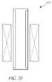
- FIG. 19Adepicts an example schematic top view of a radiation hardness structure processed with a controlled particle beam.
- FIG. 19Bis a schematic cross-sectional view of the radiation hardness structure of FIG. 19A taken along line 19 B- 19 B.
- FIG. 20depicts an exploded cross-sectional schematic view of an objective lens assembly.
- FIGS. 21A through 21Gschematically depict beam writing strategies.
- Focused ion beam (FIB) systemsgenerally do not have sufficient ion exposure to support high throughput manufacturing. Furthermore, only relatively low speed deflection is available using existing ion optics/deflection electronics methodologies, preventing efficient direct write of layers patterned for semiconductor devices. As such, FIB has been limited to mask (e.g., reticle) and semiconductor repair. As FIB technology progressed, it supported the ability to simultaneously deposit, etch, and implant patterns directly on workpieces without the use of resist.
- maske.g., reticle
- the physical properties of a beam of charged particles traveling along an axis with a distribution transverse to the axiscan be modified to provide a high speed, digital (or “pulsed”) distributed writing beam.
- Various methodscan be used to create a wave of temporally and spatially defined high-density charged particle nodes and low density (or no density) anti-nodes, traveling in a longitudinal path of accelerated particles (herein referred to as a “digitized beam”).
- a beam bunchercan be used to create localized groups (or “flashes” or “packets”) of the charged particles. These groups of charged particles may contain one or more charged particles.
- the digital beamis then passed through a deflector, whereupon variations in voltage cause the groups of charged particles to change position relative to the direction of propagation. Changes in voltage can be timed in phase with the particle nodes, thereby yielding efficient deflection. The presence of a sharp edge of the antinode effectively provides fast beam blanking for direct write.
- Applying the digitized beam to the surface of a workpieceallows resistless patterned processing, including deposition, etching, and/or implantation of material to the surface of the workpiece and/or high resolution resist exposure.
- FIG. 1Ais a perspective view of an example apparatus 100 in accordance with certain embodiments disclosed herein.
- FIG. 1Bis a top schematic view of the apparatus 100 of FIG. 1A .
- the apparatus 100comprises an exposure chamber 102 , a load lock chamber 104 , a transport module 106 , and a plurality of processing chambers 108 .
- the apparatus 100comprises a gas manifold system and an automated process controller, described in more detail below.
- the load lock chamber 104may house workpieces 101 that are not being processed, for example, before and/or after processing in the apparatus 100 .
- the load lock chamber 104is configured to achieve vacuum such that an automated material handling system (AMHS) 110 of the transport module 106 in communication with the load lock chamber 104 may insert and/or remove workpieces 101 without having to be pumped down to or up from vacuum between each transfer.
- the loadlock chamber 104is configured to accept a front opening unified pod (FOUP).
- FOUPfront opening unified pod
- the transport module 106is configured to move workpieces 101 within the apparatus 100 .
- the transport module 106comprises an AMHS 110 configured to manipulate at least one workpiece 101 .
- a suitable AMHS 110can be chosen based on the design of the exposure chamber 102 , the loadlock chamber 104 , the transport module 106 , and/or the process chambers 108 .
- the AMHS 110comprises a plurality of transport arms such that workpieces 101 may be manipulated simultaneously (or in parallel).
- the transport module 106includes a workpiece prealigner, such that the workpieces 101 removed by the transport arm 110 and subsequently placed into the exposure chamber 102 or a process chamber 108 are in an orientation that is ready for processing in the exposure chamber 102 or a process chamber 108 .
- the prealignermay use charge-coupled device (CCD) or other imaging devices to locate a flat, notch, or other identifying feature of the workpiece 101 .
- the prealigneris configured to determine overlay parameters of alignment features on the workpiece 101 .
- the overlay parametersmay comprise x and y offset, rotation, etc.
- a variety of vacuum and handling systemscan be used in the apparatus 100 .
- a system capable of processing a variety of workpiecespreferably uses a high speed workpiece handling system.
- Workpiece-into-vacuum throughputcan be increased by aligning the workpiece under vacuum on the workpiece stage instead of outside the vacuum system.
- a standard workpiece holdere.g., a wafer magazine
- Alignment of the workpiece 101 under vacuummay increase wafer into vacuum throughput.
- the transport module 106comprises one or more processing substations, for example comprise one or more buffer zones to hold workpieces 101 between processing steps, a particle contamination detector, a temperature quenching station, and/or a metrology station.
- the metrology stationmay be selected from any tool appropriate for that type of workpiece, including, but not limited to, an energy dispersive analyzer (EDS), a wavelength dispersive analyze (WDS), a secondary ion mass spectrometer (SIMS), a scanning electron microscope (SEM), a two-dimensional laser scanning imager, a three-dimensional imaging laser radar (LADAR), a thermal imager, a millimeter wave imager, a workpiece imager, and a camera.
- EDSenergy dispersive analyzer
- WDSwavelength dispersive analyze
- SIMSsecondary ion mass spectrometer
- SEMscanning electron microscope
- LADARthree-dimensional imaging laser radar
- the exposure chamber 102is configured to expose a workpiece 101 to a digital beam of charged particles.
- the exposure chamber 102comprises a beam column 200 , illustrated in more detail in FIG. 3A .
- the beam column 200comprises a charged particle source 202 for generating a stream of charged particles.
- Charged particlesmay include one or more species of positively and negatively charged ions, as well as singly, doubly, triply, etc. charged ions.
- the charged particle source 202is adapted to generate a plurality of ion species.
- the charged particle source 202is adapted to provide a current of 1,000 amperes/cm 2 (A/cm 2 ) focused to a 10 nm spot as measured at the target.
- Liquid metal ion source (LMIS) technologyenables the formation of high current density charged particle beams.
- An example technique to create a LMISis a heated reservoir of liquid metal from which a needle protrudes downward. The metal flows down the needle by capillary action. An electric field from an extraction electrode pulls the liquid at the tip of the needle into a sharp cusp (a “Taylor Cone”) from which ions are emitted.
- the point sourceis very bright (e.g., about 10 9 A/steradian/cm 2 ), and, with suitable optics, permits the beam diameter to be as small as 2 nm.
- a variety of alloysprovides several ion species common for semiconductor fabrication.
- Accelerating and focusing a distributed energy of ionscan introduce chromatic aberrations resulting in a loss of current density efficiency of the ion optic system.
- the ion beam energy distributioncan be measured as the beam full-width-half-max (FWHM) and can be distributed as much as 12%. Improving the current density efficiency and resolving long and short term stability issues can make LMIS performance adequate for a semiconductor processing tool.
- One aspect of various embodiments of the present inventionis the realization that beams of charged particles are composed of a distribution of high and low energy trails, which can be advantageously grouped.
- At least two mechanismscan contribute to the broadening of the energy distributions: first, effects related to the formation of the ions; and second, space charge forces after ion formation.
- Ion emissions from a LMIS sourceare formed either by direct field desorption of an ion at the emitter tip or by field ionization of desorbed atoms at some distance from the emitter tip. Ions generated close to the tip surface can exchange charge with neutral atoms further downstream, forcing a zero energy ion at that point. Since the electric field in the emitter area is high (e.g., between about 20 and 50 Volts/nm), ions formed at different distances from the emitter can have different energies. Space charge effects broaden the energy distribution of the beam, particularly at low velocities. Therefore, the column 200 preferably is configured to accelerate the ions to full energy directly after formation. The use of low-mass species may aid in ion acceleration when the use of such species is appropriate.
- the width of the energy distributionis preferably proportional to the current to the 2 ⁇ 3 power.
- a limitation on the maximum current density achievable with LMIS-based systemsresults from the energy distribution of the ion beam that is caused by the achromatic aberration in the upper ion optical system.
- the use of a beam digitizer 206 downstream of the charged particle source 202 that is configured to adjust the longitudinal spacing between charged particles so as to create temporally and spatially resolved groups of the charged particles along the axis of propagationcan effectively slow faster moving particles and can speed slower moving particles to obtain a uniform velocity, and thus a uniform energy distribution (accelerating voltage) within each group of the digital beam, thereby reducing the effect of the charged particle source chromatic aberration, as illustrated in FIG. 3B .
- LMIS Taylor cone emissionSimilar to the drift of an electron beam, a LMIS Taylor cone emission unpredictably drifts in a figure-8 pattern over about a one hour period. Undetected, this drift can cause pattern placement errors.
- Source lifetime and current stabilityare barriers to the practical application for production throughput processing tools using traditional LMIS sources. Further improvements at the charged particle source 202 can improve the stability and lifetime, thereby reducing frequent source replacement.
- the broadening of the energy distribution associated with ion formationcan be reduced or minimized by operating the LMIS at low temperature, thereby decreasing the neutral atom density in the proximity of the tip.
- the energy distributioncan also be reduced or minimized by choosing a low vapor pressure species, for example by selecting a doubly ionized species that has a low charge exchange cross-section and that is formed at the surface of the tip, known to have a narrow energy distribution, and by using a species that has the additional benefit of a small virtual source. It will be appreciated that other techniques can also be used.
- extended lifetime of the charged particle source 202may be achieved by conditioning the source driving parameters prior to operation.
- the incorporation of an automated conditioning routinecan contribute to the extended life and stability of the charged particle source 202 .
- a continuous flow strategysuch as impregnated electrode-type needles with hardened tips, can further extend the life span of the charged particle source 202 .
- Second order effects of improved life spancan include emission current and position stability improvement.
- Source emission position stabilitycan be successfully corrected by using an error feedback from occasional beam registrations and adjustment to source servomotors. Although increased ion beam current density is preferred, the column 200 in the exposure chamber 102 need not increase the beam current density.
- the charged particle source 202may comprise a plasma ion source (PIS), a volume plasma ion source (VPIS), a gas field ionization source (GFIS), a carbon nanotube field emitter, a free electron laser and a target, a pulsed laser ablation ion source, a magnetically confined plasma anode source (MAP), and a thermal field emission (TFE) electron source.
- PISplasma ion source
- VPISvolume plasma ion source
- GFISgas field ionization source
- a carbon nanotube field emittera free electron laser and a target
- MAPmagnetically confined plasma anode source
- TFEthermal field emission
- the stream of charged particles emanating from the charged particle source 202is collimated and directed along a axis by a collimator 204 .
- a variety of collimators 204 comprising a combination of optical elementsare appropriate for use in the column 200 .
- the collimator 204may comprise two or more lenses or a lens and a reflective optic.
- the collimator 204may further comprise an aperture configured to shape the charged particle beam.
- the collimatoris adapted to direct the charged particle stream at accelerating potentials between about 5 and 30 kilo electron volts (keV).
- the exposure chamber 102is adapted to direct the charged particle stream at accelerating potentials between about 5 and 500 keV.
- a voltage of the collimator 204is additive to additional voltages, for example applied by a lower column exit aperture.
- a mass separatorcan be configured to deflect selected ion species into a mass separator aperture plate.
- the mass separatoris preferably disposed between the collimator 204 and the beam digitizer 206 .
- the mass separatorcomprises a reflective optic.
- the mass separatorcomprises an ExB lens.
- the mass separatorcomprises a Wein filter.
- the beam digitizer 206is configured to create a digital beam comprising discrete groups of at least one charged particle by adjusting the longitudinal spacing between charged particles along the axis of propagation. In certain embodiments, the beam digitizer 206 is configured to create groups comprising between about 1 and 7,000,000 charged particles, between about 1 and 100,000 charged particles, between about 1 and 10,000 charged particles, or between about 1 and 50,000 charged particles.
- the beam digitizer 206is configured to create longitudinal spacing D between groups of charged particles of less than about 10 m of beam travel, less than about 1 m of beam travel, less than about 10 cm of beam travel, less than about 10 mm of beam travel, less than about 1 mm of beam travel, less than about 500 ⁇ m of beam travel, less than about 300 ⁇ m of beam travel, less than about 100 ⁇ m of beam travel, less than about 10 ⁇ m of beam travel, less than about 100 nm of beam travel, less than about 10 nm of beam travel, or less than about 1 nm of beam travel between the groups of charged particles.
- the beam digitizer 206is configured to create longitudinal spacing between the groups of charged particles of between about 1 nm and 10 m of beam travel, between about 1 nm and 1 m of beam travel, between about 1 nm and 10 cm of beam travel, between about 1 nm and 10 mm of beam travel, between about 1 nm and 1 mm of beam travel, between about 1 nm and 500 ⁇ m of beam travel, between about 1 nm and 300 ⁇ m of beam travel, between about 1 nm and 100 ⁇ m of beam travel, between about 1 nm and 10 ⁇ m of beam travel, between about 1 nm and 100 nm of beam travel or between about 1 nm and 10 nm of beam travel.
- the longitudinal spacing between the groups of charged particlesmay be substantially equal, unequal, periodic, harmonic, etc.
- the beam digitizer 206comprises a beam buncher.
- a stream of charged particlespass through a buncher gap where they are acted upon by an alternating potential, RF or multiple modulating potential wave forms, beat wave, harmonic, variable, or a combination thereof.
- Velocity modulationcompresses the charged particles together so that they form spatially and temporally resolved discrete groups of charged particles.
- the frequency and the buncher gap lengthare configured to match a mean velocity of the groups of charged particles.
- the applied potentialmodulates the longitudinal velocity of each charged particle as they pass through the buncher gap so that some charged particles (e.g., charged particles with a lower velocity than the mean velocity) are accelerated while other charged particles (e.g., charged particles with a higher velocity than the mean velocity) are decelerated (e.g., as depicted in FIG. 3B ).
- the gap length of the buncher gap, the magnitude and frequency of the applied potential, and the time of flight (TOF) of the charged particles through the column 200determine the final characteristics of the digital beam and the groups of charged particles at the surface of the workpiece 101 .
- FIG. 3Cschematically depicts a stream of charged particles traveling through a beam buncher.
- a potentialcan be applied across the electrodes 302 , 304 of the beam buncher that are separated by buncher gap G. If unaltered thereafter, the charged particles begin to form groups whose length L and separation (spacing) D depend on how far the charged particles have traveled after passing through the beam buncher.
- the beam buncheris configured to compress the charged particles into groups during travel.
- the beam buncheris configured to apply an electric field to longitudinally compress the groups of charged particles.
- the charged particlesare preferably fully compressed in the longitudinal direction when they reach the workpiece 101 (e.g., as depicted in FIG. 3C ).
- the energy applied by the bunchercan be determined by the difference between the initial energy of the stream of charged particles and the final energy of the temporally and spatially resolved groups of the charged particles.
- the beam bunchercomprises a plurality of buncher electrodes and therefore a plurality of buncher gaps.
- the potentialcan be selectively applied across two of the electrodes in order to change the characteristics of the digital beam. For example, a potential can be applied across electrodes with a buncher gap G of 1 ⁇ m to create nodes with a lower charged particle density and applied across electrodes with a buncher gap G of 3 cm to create nodes with a higher charged particle density.
- beam buncher input parameterssuch as beam energy and buncher current, frequency, and gap length and beam buncher output characteristics such as separation D, length L, and density are well known.
- the beam buncheris preferably operated to provide a given number of charged particles per group. First, the buncher gap, frequency, and beam energy can be held constant while the current is adjusted. Second, the beam energy and buncher current can be held constant while the buncher gap and frequency are adjusted. Other operation configurations are also possible.
- the beam bunchercomprises a helical coil that is modulated with a current frequency, resulting in a magnetic field.
- the longitudinal spacing (“gap”) between turns of the coil, the magnitude and frequency of the applied current, and the time of flight (TOF) of the charged particles through the column 200determine the final characteristics of the digital beam at the surface of the workpiece 101 .
- the frequency and longitudinal spacing between turns of the coilare configured to match a mean velocity of the digital beam.
- Bunching charged particlesallows write strategy optimization with dose variations at the charged particle level by varying the beam buncher frequency, amplitude, and duty cycle, which in turn varies the charged particle density, as described above.
- the beam buncher parametersare therefore preferably adjusted according to the write strategy.
- the beam digitizer 206comprises a beam blanker (e.g., a beam blanker that can operate at speeds sufficient to create a digital beam).
- the high speed blankermay comprise an aperture plate configured to absorb the charged particle beam at certain intervals. The aperture plate is initially positioned such that the stream flows through the aperture in the aperture plate proximate to an interior edge of the aperture plate. An electrode is configured to deflect the stream into the aperture plate, which intercepts the flow of particles to create a temporally and spatially resolved digital beam.
- FIG. 3Dschematically depicts a stream of charged particles traveling through a high speed blanker. An aperture plate 316 is positioned proximate to the stream of charged particles.
- the electrodes 312 , 314are configured to apply a potential to the charged particle stream to create temporally and spatially resolved groups of charged particles of the digital beam. If unaltered thereafter, the charged particles continue to travel with length L and separation D regardless of how far the charged particles have traveled after passing through the high speed blanker.
- the beam digitizer 206is configured to modulate an on/off state of the charged particle source 202 . In some embodiments, the beam digitizer 206 is configured to modulate a position of the charged particle source 202 longitudinal to the axis so as to displace the groups of charged particles.
- the beam digitizer 206is configured to apply electromagnetic radiation, for example with a frequency of between about 1 megahertz (MHz) and 100 gigahertz (GHz) or between about 1 MHz and 25 GHz. In such an embodiment, the beam digitizer 206 can be configured to modulate, for example, the amplitude of the electromagnetic radiation, the frequency of the electromagnetic radiation, combinations thereof, and the like. In some embodiments, the beam digitizer 206 is configured to apply a beat wave to a plasma comprising the charged particles. In some embodiments, the beam digitizer 206 is configured to apply space charges to wake fields. In such embodiments, the beam digitizer 206 can be configured to resonantly absorb the space charges.
- MHzmegahertz
- GHzgigahertz
- the beam digitizer 206is configured to blank the beam through an absorption aperture. In some embodiments, the beam digitizer 206 is configured to apply a pulsed incident neutralizing beam to the charged particle source 202 . In some embodiments, the beam digitizer 206 is configured to apply a pulsed laser beam to the charged particle source 202 .
- the column 200comprises a beam blanker downstream of the collimator 204 and a beam buncher downstream of the beam blanker.
- a digital beam coming from the beam blanker and into the beam bunchercan be used to further temporally and spatially resolve the individual groups in the digital beam.
- the column 200comprises a beam buncher downstream of the collimator 204 and a beam blanker downstream of the beam buncher. Other configurations are also possible.
- the column 200further comprises a deflector 210 downstream of the beam digitizer 206 .
- the deflector 210comprises a series of deflection stages (e.g., electrode stages, magnetic stages) disposed longitudinally along the axis of the digital beam.
- the deflector 210deflects individual groups of charged particles in the digital beam.
- the phrase “minor field deflection”refers to the deflection of an individual group of charged particles by the deflector 210 .
- the deflector 210is configured to deflect the groups in the digital beam substantially perpendicularly to the axis of propagation. In certain embodiments, the deflector comprises between about 1 and 1,000 or four deflection stages.
- the deflectorcomprises at least one, two, three, or four deflection stages. In some embodiments, each deflection stage comprises two or more electrodes. In some embodiments, one or more deflection stage comprises four electrodes. Other quantities of deflection stages and electrodes are also possible.
- an average or mean velocity of the groups of charged particles in a digital beamis between about 1 ⁇ 10 4 meters/second (m/s) and 3 ⁇ 10 8 m/s.
- application of potentials by each of the deflection electrode stagesis adapted to be synchronized with the mean velocity of the groups of charged particles passing through the deflector.
- a deflection electrode stagemay be adapted to apply a voltage only when a group of charged particles is passing through the deflector in general and through that particular deflection electrode stage in particular.
- application potentials by each of the deflection electrode stagesis adapted to be harmonically synchronized with a mean velocity of the groups of charged particles passing through the deflector.
- each deflection electrode stage in at least a portion of the deflectormay be adapted to apply a voltage only when a particular group of charged particles is passing through the deflector in general and through that particular deflection electrode stage in particular.
- application of potentials by each of the deflection electrode stagesis adapted to be randomly synchronized with a mean velocity of the groups of charged particles passing through the deflector.
- the phrase randomly synchronizedis to be given its broadest possible meaning including, but not limited to, synchronization of application of voltage by the deflection electrode stages to groups of charged particles with random spacing or synchronization of application of voltage by random deflection electrode stages to groups of charged particles with random or other spacing.
- electrodes of the deflection stageapply a substantially equal voltage potential as each group of charged particles of the digital beam passes.
- the amount of deflection of each group of charged particlesdepends on the number of electrodes activated sequentially.
- variable potentialsare applied to each deflection electrode stage as each group of charged particles passes. For example, the first deflection electrode stage has the smallest voltage with subsequent electrodes have progressively more voltage, resulting in a linear deflection as electrodes are activated. The converse is also possible, where the first deflection electrode stage has the largest voltage with subsequent electrodes having progressively less voltage.
- the number of deflection electrode stages activateddefines the amount of deflection of each group of charged particles of the digital beam.
- the signal timing and nominal voltages applied to the deflectorcan be calibrated for individual deflection electrode stages and even individual electrodes within each deflection electrode stage. Triggering an applied voltage of individual deflection electrode stages can be delayed if needed to match the incidence of to each group of charged particles of the digital beam (“phase-matching”), for example due to changes in charged particle velocity, species, and mass, deflection stage position, pattern resolution, pattern field errors, errors within an objective deflection field, process specific compensation and write strategies, combinations thereof, and the like.
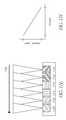
- a field perimeter of the deflection electrode stagesis defined as the minor deflection field of less then 4 mm, less than 2 mm, less than 1 mm, or less than 100 ⁇ m displacement in x or y from the center of the axis of propagation.
- the potentials of each of the deflection electrode stagesare adapted to partially displace the groups of charged particles towards an intended trajectory.
- Each groupis partially deflected 1/Nth of an intended deflection distance by each of a number N of deflection electrode stages.
- the first deflection electrode stage, or any single deflection electrode stageis adapted to substantially fully displace one or more (e.g., all) groups of charged particles towards an intended trajectory, and the other deflection electrode stages are used to fine tune the deflection of the groups.
- Other combinationsare also possible.
- the deflectorcomprises N sets of deflection electrode stages, each set of deflection electrode stage comprising N deflection electrodes, in which every Nth deflection electrode stage is configured to displace a particular group of charged particles towards an intended trajectory. If at least a portion of the deflector comprises two sets of deflection electrode stages, every other deflection electrode stage in the sets of deflection electrode stages may be configured to displace a particular group of charged particles towards an intended trajectory. If at least a portion of the deflector comprises three sets of deflection electrode stages, every third deflection electrode stage in the sets of deflection electrode stages may be configured to displace a particular group of charged particles towards an intended trajectory. Other variations and configurations are possible.
- FIG. 6Adepicts a top schematic view of a deflector 210 comprising at least one electrode in each deflection electrode stage.
- the digital beam comprising charged particlesis configured to flow through the center aperture of the deflector 602 .
- the sets of electrodes 604 , 606 and 608 , 610may be positively or negatively charged such groups of charged particles are deflected perpendicularly to the longitudinal axis of the deflector and the path.
- the electrodes on opposing sides, for instance, electrodes 604 and 606are oppositely charged.
- FIG. 6Bis a perspective quarter cut-away view of the upper right quadrant of the deflector 210 .
- the electrodes 606are separated in this embodiment by an insulator 612 .
- the deflector 210may comprise a series of deflectors, each comprising one or more deflection electrode stages.
- a deflector 210may comprise three sets of deflectors. As illustrated in FIG. 6B , the groups of charged particles are deflected by each deflection electrode stage as they travel along the path. Other deflector and electrode configurations are possible.
- the deflector 210is configured to arrange the groups of charged particles into a three-dimensional timespace (an “adaptable virtual digital stencil”). In certain embodiments, the deflector 210 is adapted to create a laterally distributed pattern of the groups of charged particles. In some embodiments, the deflector 210 further comprises a deflector lens adapted to demagnify the pattern or the virtual stencil.
- the deflector lensmay comprise an electrostatic lens, an electromagnetic lens, a reflective lens, a combination reflective and refractive lens, a combination reflective and deflective lens, a combination deflective and refractive lens, combinations of the same, and the like.
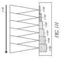
- FIG. 7is a schematic block diagram of a column 200 in which the groups of charged particles coming out of the deflector 210 are arranged in a virtual digital stencil 702 , each group of charged particles having undergone a minor field deflection.
- the objective lens assembly 212is configured to deflect the virtual stencil with a major field deflection. The combination of minor field deflection, major field deflection, and movement of the workpiece 101 can be used to expose a pattern of charged particles on the workpiece 101 .
- a phase of the groups of charged particles of the digital beam longitudinal to the axisis configured to be substantially equal, single harmonic, multiple harmonic, random, combinations thereof, and the like.
- the spacing between the deflection stagesmay be adapted to be synchronized and to be in phase with the groups of charged particles.
- longitudinal positions of the deflection electrode stagesare adjustable.
- the deflector 210comprises a digital feedback system, for example to adjust the spacing between the deflection electrode stages. Piezos, etc. may be used to position the electrodes or deflection stages.
- the column 200further comprises an objective lens assembly 212 disposed between the deflector 210 and the workpiece stage 214 .
- the objective 212may comprise a lens, a mirror, a reflective optic, a combination reflective optic and refractive lens, a combination reflective optic and deflection electrodes, a combination deflection electrode and refractive lens, combinations of the same, and the like.
- the objective lens assembly 212comprises a detractive lens assembly or a deflector electrode assembly configured to demagnify, focus, and/or deflect the groups of charged particles or the adaptable virtual digital stencil.
- groups of charged particles having a diameter (or “spot size”) of about 200 nmare reduced 10 times to a diameter of about 20 nm.
- the objective lens assembly 212may also be adapted to demagnify the groups or the stencil by 100 times or 1,000 times.
- the deflectionmay be called a “major field” deflection.
- a field perimeter of the objective lens assembly 212is defined as the major deflection field of less then 10 mm, less than 5 mm, less than 1 mm, or less than 100 ⁇ m displacement in x or y from the center of the axis of propagation.
- the exit aperturecomprises an exit aperture.
- the exposure chamber 102comprises a workpiece stage 214 downstream of the lower objective lens assembly 212 .
- the workpiece stage 214is configured to hold the workpiece 101 .
- the workpiece stage 214comprises an interferometric stage, wherein the relative position of the stage is measured using optical interference.
- the workpiece stage 214may be thermally controlled to reduce magnification errors in the workpiece, which can lead to overlay errors.
- the workpiece stageis preferably configured to continuously move while a workpiece 101 is exposed to the groups of charged particles.
- the workpiece stage 214may be configured to move continuously over a dimension of 25 centimeters over a period of 1 second during exposing.
- the workpiece stagemay be configured to move without stopping for more than 5 nanoseconds per 0.5 seconds during exposing. The ability to continuously expose while moving the workpiece stage 214 without stopping can yield increase efficiency and throughput.
- the workpiece stage 214comprises an interferometer configured to determine the location of the workpiece stage 214 in a horizontal plane.
- the relative x/y position of the stagecan be measured using optical interference.
- the workpiece stagemay comprise a registration mark, grid, or feature detectable by a secondary ion mass spectrometer (SIMS), backscattered electronics, or faraday cup disposed below the registration grid.
- SIMSsecondary ion mass spectrometer
- the registration markis preferably included in an assembly that can be moved parallel to the column 200 in order to optimize a working height of the registration mark to the workpiece, thereby reducing column calibration and registration errors.
- the digital beammay periodically or randomly be directed towards the registration mark to check the alignment of the column.
- the registration markmay also be used to calibrate the column 200 before, after, and/or during exposing a workpiece.
- the chamber 102further comprises a height control system that measures the height of the workpiece stage 214 and/or a registration mark.
- the height control systemcan include, for example, a laser and a plurality of detectors configured to receive light emitted from the laser and reflected by the workpiece, the workpiece stage 214 , and/or a surface that moves with the workpiece.
- the height control systemcan compensate for variation in the measured height of the workpiece stage by adjusting an elevation of the stage, for example by using electrostatic clamps, piezoelectric devices, etc.
- the height control systemis configured to compensate for height variations of less than 1 ⁇ m. Electrostatic clamping may be used to secure the workpiece to the workpiece stage 214 and to ensure adequate thermal contact and flatness of the workpiece.
- Full motion writingcan eliminate the workpiece stage motion overhead time while exposing a workpiece.
- the deflector 210 systemis updated in real time to track the motion of the workpiece stage 214 , thereby allowing the system to write patterns while the workpiece stage is in motion.
- Such a processpreferably uses a high speed optical controller (e.g., laser) to track the position of the workpiece stage 214 .
- a high speed optical controllere.g., laser
- circuitry on the controllercan convert Doppler-shifted laser deflection measurements into laser pulses that can be stored in a stage position register. Interferometry, laser deflection measurements, or other optical techniques can be used to track the position of the workpiece. Therefore, the throughput of lithography systems can be improved by reducing or eliminating nonexposure time during stage repositioning and settling sequences.
- each deflection field centeris defined by a window of opportunity (WOO).
- WOOwindow of opportunity
- a stage controllersignals a deflection controller to initiate exposure.
- the workpieceis exposed while the undeflected beam center passes through the WOO.
- the deflection systemcan deflect to the outer limit of the field.
- the deflection systemis updated by the workpiece stage position register of the actual location of the workpiece stage.
- the workpiece stagecan allow real time deflection correction.
- the systemcan be dynamically optimized for continuous writing.
- a typical frame/WOO densityis depicted in FIG. 4A .
- the workpiece stagemay be configured to provide suitable velocity performance, for example at 100 centimeters per second.
- the workpiece stagemay be configured to rotate a workpiece during exposure at up to about 40,000 rotations per minute (rpm).
- the workpiece stagemay have as little inertia as possible, and a compatible workpiece stage motor design can be provided.
- the use of vacuum compatible air bearing rails and linear motor drivescan provide adequate decoupling of vibration sources.
- the workpiece stage motorscan be placed in the vacuum system, light weight materials can be used for the workpiece stage, and the workpiece can be aligned on the stage, thereby eliminating the workpiece cassette and cassette clamping hardware.
- the first three derivatives of stage positioncan be limited and damped by electronic hardware to properly control the motion of the workpiece stage.
- FIG. 4Bis a schematic diagram of an example workpiece stage and control electronics.
- the exposure chamber 102may be in communication with control electronics, for example system support electronics 220 including wafer handler control, vacuum control, suspension control, temperature control, pressure control, etc. and column support electronics 230 including a source control module, digitizer control, deflector control, lens control, wafer height sensor, video processor, stage control, and a dynamic corrector (e.g., for real time column aberration correction).
- control electronicsfor example system support electronics 220 including wafer handler control, vacuum control, suspension control, temperature control, pressure control, etc.
- column support electronics 230including a source control module, digitizer control, deflector control, lens control, wafer height sensor, video processor, stage control, and a dynamic corrector (e.g., for real time column aberration correction).
- the column support electronics 230may be in communication with data process electronics 240 , for example a workstation.
- An example application of the systems described hereinis to perform in situ workpiece processing or resist exposure by directly writing on the workpiece.
- accurate registration of optics to the target workpieceis achieved, but tool induced shift (TIS) and workpiece induced shift (WIS) errors may be introduced due to temperature effects, workpiece processing effects, and optical distortions.
- An example solutionis to measure an initial pattern (e.g., one or more alignment marks) on the workpiece is and to use the measurement data to accurately place a newly patterned image onto the workpiece, for example by adjusting the exposure parameters.
- a registration sensorpreferably can automatically detect and recognize a variety of registration and alignment mark patterns, materials, and profiles without impacting the quality of exposure throughput.
- Examples to achieve such a sensorinclude, but are not limited to, using a high resolution, high speed registration system with existing hardware, determine the limitation and flexibility of the registration strategy (e.g., by mapping the workpiece with die-to-die registration) and the incorporating a temperature conditioning stage, and introducing a high speed moiré (grating) interferometer system for die-to-die registration, combinations thereof, and the like. Other approaches are also possible.
- a high resolution, high speed registration systemcan employ existing hardware and can be similar to existing electron beam registration, but a plurality of imaging modes can be used. Scanning the surface of an object (e.g., a registration or alignment mark) with a digital beam produces secondary electron emission, secondary ion emission, and ion sputtering.
- a bi-axial or cylindrical microchannel platecan be used to detect both secondary electrons (e.g., by biasing above the voltage of the target) and the secondary ions (e.g., by biasing below the voltage of the target). Other configurations are also possible.
- An imagecan be created by measuring a signal yield of the secondary ions and secondary electrons at each point where the beam impacts the target. Variations in the yield indicate changes in surface topology or composition of the workpiece.
- the position resolution of this signalis a product of the measured beam spot size and deflection pixel size during registration and is augmented by statistical metrology.
- Sputtered ionsprovide greater mark recognition ability because such ions can be collected and mass analyzed secondary ion mass spectroscopy (SIMS).
- SIMS registration techniquesare well developed and can be used both for mark detection and for process development diagnostics.
- An atomic map with the spatial resolution of the beam spot sizecan provide excellent precision for mark detection.
- a product summation of the detector video signal with a computer generated image of the registration or alignment markcan be used to enhance or recover an otherwise unrecognizable target signal from high-noise background. This can be performed by automatically correlating the video gain and bias offset for an initial signal enhancement. Once the tone is properly adjusted, the signal can be correlated with a computer generated (CAD) image of the registration or alignment mark to provide an enhanced image of the mark.
- CADcomputer generated
- Other signalsare detectable from digital beam mark interaction. Signals such as those from secondary electrons and backscatter electrons may be used for this process. Additionally, signals from secondary electrons and backscatter electron may be employed differentially to improve detection limits (e.g., signal to noise ratios). For example, the final detection signal may be the difference between SIMS and other signals.
- the speed of registrationmay be limited by the quality of the registration electronics, but incorporating modern electronics (e.g., digital signal processing (DSP)) may reduce the registration time by orders of magnitude without burdening registration resolution.
- DSPdigital signal processing
- Workpiece mappinggenerally registers a single die, providing reduced or minimum overhead to the system throughput but no correction for pattern distortion caused by temperature instability during exposing.
- Die-to-die registration performed immediately prior to die exposurefor example to minimize temperature distortion effects, generally uses four registrations per die per level.
- Such a techniqueeliminates the ability to write in a serpentine mode, drastically limiting the throughput of the system by memory load overhead time.
- performing registration on a plurality of dies at one timecan maintain the ability to write in a serpentine mode within a field comprising the plurality of dies, thereby allowing increased or maximum throughput while reducing or minimizing pattern distortion.
- the direct exposure of multi-level patterns on a single workpiece for manufacturing of integrated circuitsdesirably includes accurate intra-layer registration.
- An example workpiece alignment techniquehas three features: adequate signal generation from the surface impact of the digital beam; a detection algorithm for processing the detected signal; and an alignment feature fabrication technique.
- the impact of a charged particle onto the workpiececan create media such as secondary electrons, backscattered electrons, photons, and secondary ions, each having certain advantages in detection efficiency.
- selection of a particular media for registration purposesdepends on the charged particle species, the charged particle energy, and the current density of the beam.
- a signal detectormay be optimized for a given media. For example, an electron-photomultiplier is generally appropriate for secondary electrons, a solid state diode is generally appropriate for backscattered electrons, and secondary ion mass detectors are generally appropriate for photons and secondary ions.
- a digital signal processorprocesses information from the signal detector in order to determine the location of the alignment mark.
- a traditional method of detectionincludes a one-dimensional line scan with the digital beam. As the digital beam transitions by deflection across the alignment mark, the detected video signal is modulated. Modulation occurs because differences in the alignment mark and the contour of the workpiece. Actual alignment mark location can be determined by processing the distribution of the modulated signal via a digital signal processing module.
- Another detection methodincludes an X/Y scanning mode of the digital beam to acquire a video image of the alignment mark. To achieve accurate edge detection, digital signal processing algorithms are applied. Improved detection of the alignment feature edge is accomplished through a two-dimensional imaging method that averages several frames of video data and determines the actual location of the alignment mark by gray scale signal processing.
- alignment marksare formed over the entire working area of the workpiece in the form of equally spaced two-dimensional grids.
- One construction methodis the formation of a raised multi-layered semiconductor structure consisting of layers of silicon, silicon dioxide (SiO 2 ), and polysilicon, with an alignment mark formed on the polysilicon layer of the wafer.
- an alignment markis etched into the surface of a silicon wafer and a layer of a heavy metal (e.g., tantalum or tungsten) is deposited into the trench.
- the alignment mark containing the heavy metalexhibit a high level of backscatter relative to a silicon substrate, thereby providing contour details for low energy backscatter ion detection. Selection of an appropriate alignment feature construction method depends on the signal media and the signal detector, dictated by process steps.
- a minimum of three alignment marksare preferred in order to accurately identify translation, rotation, and magnification errors.
- the measured errorsare fed back to the workpiece stage control system for correction, thereby reducing workpiece and tool induced shift errors.
- the processing of global alignment marksmay permit faster and more accurate detection of localized alignment marks by removing gross errors.
- the alignment processcan be repeated whenever the workpiece is inserted into the exposure chamber, whenever the workpiece is removed from the apparatus, between significant process steps, etc. Other techniques can also be used.
- Patterning toolstransfer large quantities of microelectronic circuit pattern data in a format that can be manipulated (e.g., converted from digital to analog) within small periods of time (e.g., nanoseconds).
- the datais typically in a format for very large scale integration (VLSI) computer aided design (CAD), as described below.
- VLSIvery large scale integration
- CADcomputer aided design
- This datais used, for example, to control the deflection by the deflector 210 , the deflector lens, the objective lens 212 , and/or movement of the workpiece stage 214 and can be adjusted to address aberrations in the optics.
- Charged particle exposure chambersmay have imperfections (e.g., aberration, deflection errors), for example due to manufacturing or installation imperfections and the physical constraints of the optics.
- Pattern distortion or deflection distortioncan result from several factors when exposing a workpiece with a digital beam. For example, thermal fluctuations in the exposure chamber 102 or in a workpiece 101 can cause magnification errors. For another example, securely clamping the workpiece 101 to the workpiece stage 214 can also cause rotational errors or can induce stresses resulting in pattern sheering. For yet another example, unrecoverable nonlinear pattern distortions can result from subsequent processing such as rapid thermal annealing. For still another example, manufacturing or installation of the optics may be imperfect (e.g., with a slight rotation relative to the workpiece stage) and the optics have certain physical constraints.
- More complex errorsmay be introduced by certain processes, for example and without limitation, tracing a large square with the digital beam may result in a pincushion or barrel shaped pattern.
- the magnitude of the errorsmay be proportional to the magnitude of the beam deflection such that they can limit the size of the deflection field and can create nonlinear distortions in system writing quality.
- the adaptable virtual digital stencilis in softcode at any given point in time. As such, the stencil is temporally and spatially adaptable to correct in real time for nonlinear pattern offset, gain, rotation, and corrections within the minor field, while being deflected in the major field. These corrections can be performed within features, die, or to the entire workpiece.
- Digital beam lithography systemspreferably can perform pattern and beam corrections to compensate for processing-induced errors on the workpiece and optical errors (e.g., coma distortion, astigmatism, image pure distortion, chromatic aberration, spherical aberration, field curvature, etc.). Such corrections can improve writing quality and enhance system throughput.
- optical errorse.g., coma distortion, astigmatism, image pure distortion, chromatic aberration, spherical aberration, field curvature, etc.
- Pattern and deflection distortion problemscan be corrected by incorporating data manipulation bias electronics (hardware and software) into the system.
- process control softwarecan use metrology measurements to correct the deflection of the digital beam.
- Such metrology measurementspreferably are made prior to exposing the workpiece.
- the quality of the digital beammay initially be optimized to provide improved or optimum measurements from subsequent metrology.
- a knife-edged micromesh gridis placed over a diode detector, which is scanned by the digital beam.
- the second derivative of the beam current with respect to the scan positionprovides a high resolution beam profile (e.g., as depicted by FIG. 4D ).
- Optimizatione.g., automated optimization
- of the beam profile with the optics control systemallows focusing of the beam.
- the systemcan correct the digital beam profile within a larger usable deflection field by moving the workpiece stage 214 to a plurality of positions within the outer limits of the distorted deflection field.
- the digital beamis then deflected to the position where the grid is scanned for beam optimization.
- the sequenceis repeated over an extended size of the deflection field.
- Beam optimization datacan then be correlated with an interferometer or other position monitoring system of the workpiece stage 214 .
- the linear contribution of the erroris stored as an argument, while the nonlinear error is stored as pure memory. Beam distortions that depend on the position of a minor field within a major field can also be correlated.
- a final measurementcan be made prior to exposing portions (e.g., individual dies) of the workpiece 101 because the workpiece 101 may be rotated or distorted as a result of temperature or stress effects caused by processing.
- portionse.g., individual dies
- the new levelcan be adjusted to overlay on the previous levels, for example by registering to three or four corners of the die and then applying a magnification or rotational correction within each die.
- the calibration softwaremay automatically measure features on the edges of each die prior to exposure and use the measurements to correct for any pattern displacement, magnification, or rotation caused while aligning, processing, or handling the workpiece.
- the exposure chamber 102can be operated by providing integrated circuit (IC) design data, for example in the form of CAD schematics, to generate and expose the pattern on the workpiece. Users of the apparatus 100 input a desired pattern to be written, along any specific alignment configurations and/or processing parameters. Once the design for a device (e.g., an integrated circuit) is developed, multiple pattern layers of the design can be laid out to cover the workpiece as desired (e.g., to cover the entire workpiece).
- a complete exposure data preparation (EDP) package with a user interfacecan be used to convert raw designs (e.g., in CAD or graphic data system (GDSII)) to a format usable by the exposure chamber 102 (e.g., exposure ready format (ERF)).
- raw designse.g., in CAD or graphic data system (GDSII)
- GDSIIgraphic data system
- a field partition routinecan define the major and minor deflection fields of the pattern data and use a smoothing routine to normalize the density in each data frame. Normalization reduces stage jerking when writing repetitious adjacent multiple density patterns.
- pattern data in GDSII, OASIS, or other suitable formatsis input into the system.
- the input datais then fractured into subfields and identified as to whether they are to be “written” or “non-written.”
- the mapping of the written subfieldsis sent to a data path module for rasterization (e.g., conversion to a bitmap).
- Throughput improvementis achieved by moving the workpiece stage and deflecting the beam from one written subfield to a non-adjacent written subfield without exposing non-written subfields. No time is spent processing non-written subfields without pattern data.
- Raster scanis a scanning mode in which the beam moves back and forth over the entire workpiece; the beam is turned on over designated areas and is turned off until the next designated area.
- Vector scanis a scanning mode in which the digital beam scans only selected areas where pattern is to be placed; after scanning of the selected area is completed, the beam is turned off and moved to selected area to be scanned.
- Hybrid vector-raster technologyutilizes a vector approach for major field deflection between data pattern subfields and uses a raster scan technology to deflect a Gaussian or shaped digital beam within the subfield. Throughput improvement can result from only moving the workpiece stage to positions that receive exposure.
- vector-rasterincludes a vector deflection in the major field, a vector deflection between pattern features within the minor field, and a raster image of the feature within the minor field.
- the vector capability of a vector-raster systemcan provide higher throughput versus a pure raster scan system, and the raster capability of the vector-raster system permits good pattern fidelity and high current with a small dwell time.
- minor field deflection of the digital beamis accomplished through a deflector, which is possible because that the longitudinal spatial and temporal spacing of the groups of charged particles permits the individual deflection of each group.
- the voltage applied to each deflection electrode stageis timed to match the velocity of each group of charged particles.
- Spacing between groups of charged particlescan effectively provide blanking.
- blanking between groupseffectively uses the full flux of a continuous or nearly continuous charged particle stream.
- the temporal spacing between groupsallows for deflection error correction (error correction signal summing can compensate for stage disposition, deflection aberrations, optical aberrations, and write mode process adjustments).
- Throughput improvementcan be achieved by maximizing the time that the digital beam exposes the workpiece.
- the digital beamis capable of performing a plurality of pattern exposure strategies. Such strategies may be designed to modify exposure dose, species, pattern quality, beam energy per group of charged particles, beam energy for sets of groups, and beam energy for an adaptable virtual digital stencil.
- the apparatusmay also be capable of discretely modifying exposure dose, species, pattern quality, beam energy per group of charged particles, beam energy for sets of groups, and beam energy for an adaptable virtual digital stencil within a particular writing strategy to optimize that particular writing strategy for a particular process.
- the beamis scanned in raster fashion across the entire area of the workpiece.
- the spot size of the beamis greater than the grid spacing in the raster (e.g., as depicted by FIG. 21A ).
- the spot size of the beamis substantially equal to the grid spacing in the raster (e.g., as depicted by FIG. 21B ). That is, the pattern is vector scanned in the major field, vector scanned in the minor field, and raster scanned in a single pass within the feature to be exposed.
- Feature processing with a digital beamcan leverage the per pixel dose variation to improve feature edge quality when performing etch, implant, and deposition.
- a digital beam spot size to pixel ratio greater than onecan average placement of the groups of charged particles and can reduce exposure process errors.
- a large digital beam spot size to pixel ratioimproves line edge roughness and allows a higher dose deposition due to cumulative dosing from overlapping beams. This process can also be performed with or without resist.
- alternating row and column exposureis performed with a large spot size and small pixel size ratio.
- Exposing alternating pixels with a digital beamproduces a pixel exposure width half as wide as the selected feature, thereby increasing the feature critical dimension over target value in both axes (e.g., as depicted in FIG. 21C ). That is, the pattern is vector scanned in the major field, vector scanned in the minor field, and raster scanned in alternating pixels in both x and y directions with a single pass within the feature to be exposed.
- Throughputis increased by effectively reducing the number of charged particles per flash, but at the cost of critical dimension control.
- Yet another embodiment of a writing strategydivides pixel spaced matrices (or “composites”) and overlays exposure of a combination of composites interleaved in a series of passes, with each pass offset from other passes in both the x and y directions by a fraction of the writing address. That is, the pattern is vector scanned in the major field, vector scanned in the minor field, and raster scanned in a series of passes that interleave the pixels within the feature to be exposed.
- the beam sizecan be set 25-100% larger than pixel size in order to average out the flashes and to reduce the number of charged particles per group (e.g., as depicted in FIG. 21D ).
- a larger beam spot size versus pixel sizehelps reduce line edge roughness by averaging systematic errors to allow a higher dose deposition (e.g., as depicted in FIG. 21E ).
- This write modefor a digital beam, such as the ability to apply per pixel dose variation to improve feature edge quality when performing direct etch, implant, and deposition processes, thereby improving feature edge quality.
- This processcan also be performed with or without resist. The feature quality is improved, but multiple passes are achieved with little or no effect on throughput.
- a writing strategyleverages a sampling matrix having an array of cells of a predetermined input address size.
- Each passproduces a writing grid defined by the distance between beam placements in a single pass. That is, the pattern is vector scanned in the major field, vector scanned in the minor field, and raster scanned in a series of passes offset in the x and y directions to create multiple offset composite feature patterns that interleave the pixels within the feature to be exposed.
- the composite of all passesforms the effective exposure grid (e.g., as depicted in FIG. 21F ).
- the dose of the beamcan also be freely varied within the operating envelope of the system.
- This processcan also be performed with or without resist with a pixel rate greater than about 400 MHz. A good balance between feature quality and throughput can thereby be achieved.
- the dose of the beamcan also be varied within the process-defined operating envelope of the system (e.g., as depicted in FIG. 21G ). This can be performed with a number of techniques including modulating the duty cycle of a beam buncher. Multiple levels of pixel intensity are provided from 0% to 100% beam intensity.
- Pixels of partial intensityare used along the edge of a feature so as to locate the edge between the lines of a Cartesian raster scan grid.
- the dose modulationcan be assigned by the user via the pattern data file.
- FIG. 8illustrates an example vector-raster write strategy using a digital beam.
- the workpieceis divided into square pixels 1 through 44 .
- the beamgenerally writes in a serpentine motion across the workpiece, from 1 to 4 , then from 5 to 12 , then from 13 to 22 , etc.
- Each pixelis divided into stripes, and each stripe is divided into fields, which are divided into subfields.
- the beamgenerally writes in a serpentine motion across each stripe, field, and subfield as well. Within each subfield, the beam is able to write only where written features exist.
- the digital beamonly scans selected areas, but the beam does not need to be turned off to be moved to another area, at least the time the beam is turned off is reduced as the dead space between the groups of charged particles can be used for that purpose.
- patterning with accurate overlayis preferably at least one order of magnitude smaller than the minimum or critical dimension.
- Workpiece processing and handlingmay induce pattern errors across the workpiece that contribute to placement errors, especially as geometries fall below 0.25 microns.
- serial patterning equipmente.g., exposure chambers with a digital beam
- a fully automated metrology programthat commands the digital beam to align itself, perform deflection/workpiece positioning calibration, and recognize and correct for wafer pattern distortion can eliminate not only pattern defects at the most recent level, but for other pattern errors, as well.
- system calibration softwarecan collect the deflection gain, linearity, offset, and rotation for both the major and minor deflection fields.
- the deflectionis calibrated to the laser interferometer system, providing a well-behaved deflection motion and profile of the digital beam within the deflection field. Linear and nonlinear errors of the digital beam profile with respect to the beam deflection can also be measured and corrected.
- temperature compensationcan be performed by adding corrections to the pattern software and exposing that die in a corrected state, which allows the system to reduce or eliminate pattern distortions caused by annealing, vacuum radiation drain and evaporation, and improper conditioning.
- EDPelectronic data preparation
- Pattern editing, tone reversal, and feature biasingprovide increased flexibility to the user of the apparatus 100 .
- feature bordering, dose by size, and dose by typecan improve digital beam assisted chemical etching (DBACE) and digital beam nucleation deposition (DBND) at small geometries.
- DBACEdigital beam assisted chemical etching
- DBNDdigital beam nucleation deposition
- a data manipulation bias systemcorrects for pattern and deflection distortion, for example by augmenting pattern data applying corrected data to the optics control system.
- the data manipulator systemapplies final pattern data biasing prior to optics control, and therefore may include very fast electronics (e.g., the fastest electronics in the system).
- This systemsums pattern data correction, deflection distortion correction, and workpiece stage motion correction to the front end of the optics control system.
- Digital to analog converters at the front end of the optics control systemconvert the digital signals from the data manipulator. Once amplified, these analog signals drive the column 200 .
- Overlay accuracycan limit sub-micron lithography.
- traditional lithography systemscannot correct for nonlinear pattern distortions caused by wafer processing, which is exacerbated by increased workpiece sizes and reduced device geometries.
- certain digital beam systems described hereincan advantageously correct for such errors because the pattern is not fixed on a reticle, but can change during exposing.
- the adaptable virtual digital stencilis in softcode at any given point in time. It is therefore temporally and spatially adaptable to correct in real time for nonlinear pattern offset, gain, rotation, and corrections within the minor field, while being deflected in the major field. These corrections can be performed within features, die, or to the entire wafer.
- a method of processing a workpiece 101 in the exposure chamber 102comprises exposing the workpiece 101 to a digital beam of charged particles.
- exposing the workpiece 101comprises forming a stream of charged particles, collimating and propagating the steam along an axis, digitizing the stream into a digital beam comprising groups (or packets or flashes) comprising at least one charged particle, deflecting the groups of charged particles using a series of deflection electrode stages disposed longitudinally along the axis, demagnifying the pattern, and focusing the demagnified pattern of groups of charged particles onto the workpiece 101 .
- the dosage of exposureis preferably less than about 1 ⁇ 10 17 charged particles/cm 2 .
- digitizing the beammay comprise, for example, beam bunching, high speed blanking, combinations thereof, and the like.
- deflecting the groups of charged particlescomprises selectively applying voltages across the deflection electrodes at each deflection electrode stage.
- Selectively applying the voltagesmay comprise applying a large voltage with a first deflection electrode stage and applying smaller voltages with other deflection electrode stages.
- Selectively applying the voltagesmay also comprise applying a small voltage with a first deflection electrode stage and applying larger voltages with other deflection electrode stages.
- Selectively applying voltagesmay also comprise applying approximately equal voltages at each deflection electrode stage.
- Demagnification of the groups of charged particlespreferably produces packet diameters of less than about 200 nm, less than about 50 nm, less than about 10 nm, less than about 5 nm, or less than about 1 nm.
- the workpiece stagemay move continuously during the exposing process.
- the workpiece stagemay move continuously over a dimension of about 100 cm over a time period of 1 second.
- the workpiece stagemay move without stopping for more than 5 nanoseconds per 0.5 seconds.
- FIG. 5illustrates a plurality of groups of charged particles 502 , 504 .
- deflection of a group of charged particlesoccurs during a dead zone 512 at the workpiece such that no exposing occurs during the deflection.
- the rise time 509 of saturated beam pulsescan be used for blank and unblank edges.
- the geometry of the groups of charged particlesare Gaussian in x and y dimensions perpendicular in time, as well as Gaussian in velocity to, the axis of propagation.
- the groups of charged particles 502 , 504have a trapezoidal cross-section along the longitudinal axis. In FIG.
- each digital beamhas a density distribution rise time 506 and a fall time 508 .
- the time between no charged particles and the peak density of charged particlesis the quick pulse rise time 509 .
- the time in which each group 502 , 504 has a peak density of charged particlesis the digital flash time 510 .
- the time between the full concentration of charged particles and no charged particlesis the quick fall time 511 .
- the time in which there are no charged particlesis the dead zone 512 (the anti-node region).
- the time between the last instance of a full concentration of charged particles in a first group, for example the group 502 , and the initial concentration of charged particles in a subsequent group, for example the group 504 ,is the deflection time 514 .
- the time between the first concentration of charged particles in a first group, for example the group 502 , and the initial concentration of charged particles for a second subsequent group, for example the group 504is the flash duty cycle (or “flash spot rate”) 516 and is used for feature-to-feature deflection time within the minor field. In some embodiments, however, blanking can occur over multiple duty cycles. A blanker may be used.
- the apparatus 100may further comprise at least one dedicated process chamber 108 .
- Additional process chamberscan optionally be used for advanced processing.
- the process chambers 108may comprise any variety of workpiece processing equipment.
- the processing chambers 108may comprise etch, deposition (e.g., oxidation, nucleation, etc.), rapid thermal anneal (RTA), combinations of the same, and the like.
- Some process chambers 108may be configured to process a workpiece 101 that has been exposed in the exposure chamber 102 , while other process chambers 108 can be configured to process a workpiece 101 before or after processing in another process chamber 108 , before processing in the exposure chamber 108 , etc.
- a process chamber 108does not substantively change the workpiece 101 .
- a process chamber 108may comprise a calibration or metrology tool.
- the apparatus 100comprises a plurality of processing chambers 108 such that a workpiece 101 may be transformed from a bare substrate to a substantially finished product.
- workpiece 101can be fully processed without being removed from the apparatus 100 .
- the duration from starting substrate to substantially finished productis less than one week, more preferably less than two days, or even more preferably less than one day, or more preferably yet in less than one hour.
- two process chambers 108are dedicated to nucleation and oxidation deposition, a third process chamber 108 is dedicated to rapid thermal annealing, and a fourth process chamber 108 is dedicated to chemically-assisted digital beam etching (CADBE).
- CADBEchemically-assisted digital beam etching
- Automated processing softwarecan be used to monitor and analyze all aspects of the system's performance, to perform automation control of all functional operations, and to optimize each process performed by the system.
- the softwarecan perform a data gathering routine on all sensors of the system and organize the results into operational and performance related reports addressing the status of the system.
- the softwarecan also prepare a processing report for each workpiece processed through the system including the targeted process compared to the actual process, which can be used to determine fault analysis and process boundaries. Feedback of the process parameters into an automated control loop (e.g., a knowledge based routine) allows high leverage in developing processes.
- the softwaremay incorporate data gathered from one or more metrology processes to enhance such process development, for example to monitor and adjust etching rates, deposition thicknesses, and contamination.
- the softwarecan preferably operate all system functions, including process sequences, process parameters for each sequence, etc., although pattern exposure may be controlled by a pattern generation system.
- the softwarecan produce interlocks based on the process sequences and can provide full automation and optimization of the processes. Other configurations are possible. User control and adjustment is also used in certain embodiments.
- Etchingis a process for the manufacture of semiconductor circuits.
- High leverage microelectronic integrated circuitsgenerally utilize high resolution etching of materials to within a critical dimension and location.
- the ability to etch metals, semiconductors, and dielectrics with precise control over feature depth, uniformity, anisotropy, and reproducibilityis desirable for many applications.
- Standard processing techniquestypically utilize a resist-related patterning step followed by a wet or dry chemical etch to perform material removal.
- Resist patterninglimits the quality of the etch process profile, size, depth, and uniformity. Milling, or etching after exposure by a focused ion beam, provides high resolution removal of material without the use of resist. However, high dose and low sensitivity cause slow speed of the equipment, and milling has not been commercially successful. Chemically assisted processes (e.g., chemically assisted ion beam etching (CAIBE) and reactive ion etching (RIE)) were introduced to enhance milling, but they could not be incorporated into FIB equipment because the gas reacted with several components within the exposure chamber. In contrast, as described herein, low dose procedures in combination with concentrated charged particles in groups compatible with resistless processing provides quality patterns and high throughput.
- CAIBEchemically assisted ion beam etching
- RIEreactive ion etching
- etch, implant, and deposition of the workpiececan be performed within the exposure chamber 102 .
- Multiple activation by exposure to a digital beam and a process gascan dramatically improve the efficiency of all three processes.
- a digital beam specifically designed for a particular process in terms of energy, species, and current, which is possible because the digital beam parameters are adjustable,can impact and decompose a portion of the process gas molecules.
- the decomposed moleculesstrike surface atoms of the workpiece to sputter or implant new atoms into the workpiece, or to deposit new atoms on the workpiece surface.
- portions and/or all of the workpieceis heated during exposing.
- a new family of etching techniquesis ideally suitable for high resolution, high throughput microelectronics manufacturing using a resistless process.
- This new process familyis called digital beam assisted chemical etching (DBACE), and is up to 10 to 100 times more sensitive to ion exposure than milling.
- the processcomprises at least two steps including digital beam exposure of a pattern to the regions to be etched.
- the target surface of a workpieceis exposed to very low dose ion energy, creating a reactive region for the chemical agent.
- the workpieceis then introduced to reactive gas within a separate chamber.
- a high resolution dry chemical etching processactively removes the material within the desired location as a parallel process to digital beam pattern exposure on other workpieces within the exposure chamber.
- DBACEcan be performed on silicon and silicon dioxide (SiO 2 ) with chlorine (Cl 2 ) or fluorine (F 2 ) gas, on gallium arsenide (GaAs) with Cl 2 , on carbon (e.g., diamond) with oxygen (e.g., O 2 ) and nitrous oxide (N 2 O 3 ), on tungsten and molybdenum with carbon bromine trifluoride (CBrF 3 ) and high temperature superconductors (e.g., cuprates such as La 1.85 Ba 0.15 CuO 4 , YBa 2 Cu 3 O 7-x (yttrium barium copper oxide, YBCO, Y123, yttrium barium cuprate), and cuprate-perovskite ceramics with or without normal metallic regions) with wet hydroxide chemicals (e.g., sodium hydroxide (NaOH), potassium hydroxide (KOH)).
- DBACEhas been successfully applied to etch the gate recesses of gallium
- FIGS. 9A-9Cschematically illustrate an example digital beam assisted chemical etching process.
- an oxide layer 902has been deposited over gallium arsenide.
- the oxide layer 902is exposed in an exposure chamber 102 , for example with gallium ions (Ga + ), depicted as arrows 904 .
- the workpieceis then transferred to an etchant chamber.
- a chlorine (Cl 2 ) etchremoves the oxide layer that was exposed in the exposure chamber 102 , as well as underlying gallium and arsenic as gallium chloride (GaCl 2 ) and arsenic chloride (AsCl 2 ), respectively.
- the resultis a trench in the gallium arsenide, as depicted in FIG. 9C .
- other ion species and etching speciesmay be selected depending on the material or materials to be etched.
- PVDphysical vapor deposition
- CVDchemical vapor deposition
- ALDatomic later deposition
- platinge.g., electroplating
- coatinge.g., spin coating
- Deposition techniquesthat may advantageously avoid resist patterning processes by exposure to a particle beam before, during, or after the application of a deposition process include particle beam and thermally activated deposition, for example, but not limited to, digital beam activated CVD, digital beam activated thermal nucleation, digital beam activated ALD, and chemically-assisted digital beam deposition.
- IBNDion beam nucleation deposition
- CAIBDchemically assisted ion beam deposition
- In situ deposition processesprovide a variety of desired materials for the fabrication of silicon complementary metal-oxide semiconductors (CMOS), gallium arsenide, and other devices.
- CMOScomplementary metal-oxide semiconductors
- deposition throughput and film qualityare highly desired for such processes.
- CMOScomplementary metal-oxide semiconductors
- IBNDreasonable throughput deposition for wafer fabrication was not possible using in situ beam processing.
- the rate of film deposition for CAIBD using a large ion dosagee.g., 4 ⁇ 10 16 ions/cm 2
- the rate of film deposition for CAIBD using a large ion dosagewould be limited by the beam current to about 100 A/cm 2 , and it would take over 20 years to deposit one square centimeter for a layer 500 ⁇ thick.
- IBNDis able to produce desired film thicknesses while also satisfying throughput and quality concerns.
- a process resulting in 30% coverage of the usable surface of a 300 mm diameter workpiece (about 200 cm 2 ) by 2.5 ⁇ of deposited materialwould take about five seconds to expose using an exposure chamber 102 having a beam current density of 10 A/cm 2 , which can expose nucleation sites on the order of 10 cm 2 /s.
- the workpiececan then be transported to a nucleation chamber for deposition while another workpiece is exposed in the exposure chamber 102 .
- FIGS. 10A-10Cschematically illustrate an example digital beam assisted deposition process.
- a deposition chamberwhere it is exposed to reactant (e.g., a reactant fluid, preferably a reactant gas).
- reactante.g., a reactant fluid, preferably a reactant gas.
- the reactantreacts with the exposed areas to nucleate or atomically deposit a material, resulting is the workpiece of FIG. 10C with an area 1104 of deposited material.
- Integrated microelectronic manufacturing of silicon, gallium arsenide, and other electronicsutilize ion implantation to alter device mobility profiles at transistor junction edges.
- Traditional implantation techniquesgenerally include resist deposition, patterning, development, and baking, followed by ion implantation, resist removal (e.g., by ashing and/or stripping), and cleaning.
- Device fabricationuses a series of these implantation techniques, thereby requiring a large number of patterning steps. Patterning may be reduced by using serial implantation, but devices incorporating gradient implantation, lightly doped drains (LDD), and co-implantation, which can achieve higher performance, typically trade process simplification for increased device performance. For example, high resolution implantation placement accuracy may result in increased device reliability and/or process robustness.
- LDDlightly doped drains
- reticle masks used in the resist patterning stepsmay take on the order of months and tens of thousands of dollars.
- Process developmente.g., the resist exposure conditions appropriate for the reticle, resist type, resist thickness, etc.
- pilot fabricationcan take weeks or months. If testing reveals defects in the reticle design or the process steps, the process may need to start over, and iterates until a functional device can be reliably created.
- Such lengthy developmentis impractical or even impossible for certain devices (e.g., specialty military devices where a limited number of devices will be produced).
- resistless, direct write implantationcan provide the manufacturing flexibility and quick development time to incorporate advanced techniques (e.g., single-level gradient implantation, LDD, and co-implantation) in research, pilot production, and full production environments.
- advanced techniquese.g., single-level gradient implantation, LDD, and co-implantation
- Such a systemcan achieve vertical implantation profiles ranging from about 5 kilo electron volts (keV) to about 500 keV within, for example, about 20 nm.
- keVkilo electron volts
- These systemscan have the flexibility to select the species of the ion beam and to place the beam within 9 nm of itself in a gradient energy or dose profile, which can be used to achieve advanced implantation processes such as gradient implantation, LDD, and co-implantation.
- FIGS. 11A through 11Dschematically depict a cross-section of a workpiece processed with direct write implantation.
- the workpieceis implanted with a first set of digital beam exposure profile, represented by arrows 1100 in FIG. 11B .
- the resultis a workpiece of FIG. 11C with an area 1102 of doped material.
- An implantation with a second digital beam exposure profile, represented by arrows 1104 in FIG. 11Cis then performed.
- the resultis a workpiece of FIG. 11D with doped area 1102 and doped areas 1106 .
- the workpiecemay be annealed after each implantation or after the series of implantations to activate the dopants.
- the workpiece illustrated in FIG. 11Dcan be performed with a single implantation, for example using the techniques illustrated in FIGS. 11E through 11I .
- FIG. 11Ethe charged particle density of the groups of charged particles are altered as they are scanned across the workpiece, illustrated by arrow 1108 .
- Area 1110 of the workpieceis lightly doped (e.g., n ⁇ ) while area 1120 is heavily doped (e.g., n ++ ).
- FIG. 11Fis a plot of the log of dosage versus position of a workpiece similar to that of FIG. 11E .
- the dosage profilecan become linear by, for example, overlapping the beams of FIG. 11E .
- FIG. 11Gthe energy of the beam is altered as it scans across the workpiece, illustrated by arrow 1122 .
- FIG. 11His a plot of the implant depth versus position of a workpiece similar to that of FIG. 11G .
- the dosage profilecan become linear by, for example, overlapping the beams of FIG. 11G .
- the energyvaries between about 5 and 500 keV, or more preferably between about 5 and 200 keV.
- FIG. 11Ithe charged particle density of the groups and the energy of the groups are altered as the digital beam scans across the workpiece, illustrated by arrow 1136 .
- Area 1138 of the workpieceis both lightly and shallowly doped while area 1148 is both heavily and deeply doped.
- other beam parametersfor example species, may also be altered.
- the beamis altered across a transistor, across a die, or across a workpiece.
- the beamis altered within about a 20 nm area on the workpiece. Alteration of the beam may also enhance etching, deposition, and other processes.
- LDDlightly doped drain
- FIGS. 12A through 12Cdepict example schematic cross-sections of implant structures within workpieces that can be achieved with a single digital beam process step.
- Beam implantationcan also be used to improve device scaling.
- a limited factor in controlling device scalingis the source/drain junction depth. The shallower the junction, the fewer the short channel effects and the greater the degree of scalability. However, a shallow junction results in increased parasitic source/drain resistance. The impact of this source drain/resistance is appreciable for deep sub-micron devices.
- the lateral grading potential of beam exposurecan be particularly useful in this instance, for example by making a drain that is very shallow near the transistor channel yet deep under the transistor contact. The shallow junction near the channel edge results in reduced short channel effects, while the deep junction under the contact promotes low series resistance.
- Another optionis placing a deep junction on the source side and a graded junction on the drain side. This can keep the series resistance at a minimum on the source side where it is most important while reducing the negative effect of drain induced barrier lowering on the drain side.
- Lateral channel doping variations produced by digital beam implantationpermit the construction of high performance, high yield planar gate FETs.
- LDD regionsincrease the output resistance and breakdown voltage of the transistor, which increases power capability.
- increasing the doping of the source and beneath the gatecan reduce the source-gate resistance to improve the FET transconductance and gain by increasing the channel current.
- These desired lateral doping variationsillustrated by the chart of FIG. 13B , can be produced by varying the implant dose in segments along the length of the channel. The number of different segments that can be used is only limited by the digital beam size.
- GaAs FETsare a key element of many microwave (or millimeter-wave) monolithic integrated circuits (MIMIC)
- MIMICmicrowave (or millimeter-wave) monolithic integrated circuits
- other elementssuch as Schottky diodes are frequently fabricated on the same workpiece for high performance devices.
- a FET gatecannot be used as an ideal diode because the cutoff frequency is much lower than a high quality Schottky diode.
- Fabrication of FETs and Schottky diodes on the same workpieceis difficult to accomplish with either epitaxial growth or blanket implantation processing.
- Digital beam processingis well suited for selective ion implantation processing of FETs and diodes on the same workpiece because the ability to perform discrete processing at different location on the workpiece, as illustrated in FIG. 15 .
- the resulting devicesare substantially planar, which improves yield.
- other processing stepsmay be combined with traditional processes.
- GaAs MIMICsare traditionally produced using blanket implantation and deposition steps, and batch etching and alloying steps. Photoresist is used to selectively mask and define the device and circuit patterns at each level. Altogether, traditional methods employ over 25 different process steps including 12 mask levels. The front-end (topside) process alone typically takes over 240 hours to complete for a 6-workpiece batch. The process is very inefficient because of the large amount of overhead time and touch labor required.
- GaAs MIMIC processingcan be significantly improved and simplified to increase yield and lower cost by designing a digital beam process of selective pixel based implantation, deposition, and etching. Digital beam processing offers tremendous benefits in simplification and improvement of the GaAs MIMIC process, thereby leading to faster cycle times, higher circuit yields, and lower chip costs.
- an example GaAs MIMIC digital beam processcomprises selective channel and contact implants followed by annealing. Ohmic contacts are delineated and contact metal is deposited by digital beam deposition followed by digital beam isolation implant. The contacts are alloyed by annealing. Thin film resistors, FET gates, metal interconnects, insulators, and passivation layers are digital beam deposited.
- Multifunction MIMICsintegrate multiple functions in a single device.
- GaAs MFICshave been fabricated with increased levels of integration of receiver functions, combining analog and digital functions, and combining transmitter and receiver functions.
- MFICslower system cost by reducing parts count, size, weight, and assembly/tune costs.
- Wafer scale integration(WSI), which would integrate many dissimilar functions to form a complete system on a wafer, is well suited for many generation of future microelectronics.
- MFICsare generally required for advanced phased array antenna systems, which integrate complex radio frequency functions with optical control and digital signal processing.
- An exampleis the System Level Integrated Circuit (SLIC).
- SLICSystem Level Integrated Circuit
- Most of the components developed for phased array applicationsare designed individually using hybrid assembly techniques. Sufficient support functions are not integrated, hence, cannot be inserted into the system directly.
- Monolithic integration of the circuit functionsreduces part count, size, weight, and assembly costs.
- High electron mobility transistorsare heterojunction FETs with greatly improved performance over conventional GaAs FETs.
- HEMTsare generally used in high speed digital circuits and low noise amplifiers operating at millimeter-wave frequencies.
- High speed, ultra-low power digital circuitstypically have complementary n-channel and p-channel FETs fabricated on the same workpiece, which is difficult, even with selective epitaxial material growth techniques.
- Digital beam processing implantationis well suited to fabricate complementary heterojunction insulating gate (HIG) FETs on the same wafer.
- Cross-sections of the basic n and p channel HIGFET devicesare shown in FIGS. 14A and 14B , respectively. The devices are substantially planar and embedded in a semi-insulating substrate.
- a digital beam comprising siliconcan be used for the n-channel device implant, and digital beam comprising beryllium can be used for the p-channel device implant.
- the metal-silicide gatee.g., Schottky gate
- ohmic contactse.g., comprising AuGe, AuZn
- Such a sequenceallows a two step in situ device fabrication process. As a result, the unique features of the device would be a high resolution duel proximity printing with a minimum step process.
- Heterojunction bipolar transistorsare typically used in devices with high linearity, precision analog, digital/digital converter, and microwave power applications. However, current gain and maximum frequency of oscillation are limited by parasitic base resistance and collector capacitance, respectively. The performance and yield of GaAs HBT devices can be improved with selective digital beam implantation.
- FIG. 17represents an example cross-section of a workpiece under such an application. First, beryllium implants into the substrate before contact metallization reduces contact resistance. The base layer can have a lower doping concentration for the same base contact resistance, which increases the current gain by promoting electron transportation through the p-type base.
- oxygen or boron implantation between the emitter and base electrodeselectrically isolates and confines the electron current to flow vertically through the device rather than recombining laterally. This reduces stray capacitance and improves the operating frequency.
- Such fabrication processesare difficult to perform with standard photoresist processing techniques because of the small dimensions and because photoresist processing increasing surface recombination which decreases gain.
- the lateral doping capability of a beam implantcan also improve device scalability through use of channel stop implants.
- Such channel stop implantsusually reduce the effective device width of narrow transistors, reducing the junction capacitance and increasing the performance of the technology.
- difficulty in tailoring the doping concentration along the edge of the field oxidecan result in more implant than needed going into the active area.
- the implantWith a beam exposure, the implant can be spatially controlled to keep a sufficient, but not excessive, surface concentration along the field oxide edge.
- Varying the channel stop implantcan include grading a channel stop or guard ring implant along a bird's beak to prevent field inversion resulting from ionizing radiation.
- Guard ring approachesnormally result in large area penalties because the implant dose required for hardness is sufficiently high to promote breakdown problems from the close proximity of n + /p + regions. Leaving a space between the guard ring and the n + implant layers can solve this breakdown problem (e.g., as depicted in FIG. 19A ). Although effective, this approach can result in a large density penalty, especially as devices are scaled into the sub-micron regime.
- a horizontal doping gradientcan decrease the ion dosage near the junction edge, where the field oxide is thin and thus less sensitive to radiation, and can increase the ion dosage under the thicker part of the field oxide.
- Implantation of a non-conducting layercan be used to form a very dense isolation approach.
- An implantation of sufficient dosagee.g., between about 1 ⁇ 10 15 charged particles/cm 2 and 1 ⁇ 10 17 charged particles/cm 2
- forms amorphous regions with essentially infinite resistivitye.g., as depicted in FIG. 19B ).
- Devicescan thus be isolated from each other by this high resistance region.
- the dimensions of this isolation regioncan be extremely small, for example much smaller than an oxide isolation guard ring, resulting in greatly improved circuit densities.
- CMOS applicationsthe use of a bipolar transistor can be very desirable. This has led to the widespread interest in BiCMOS technology. Many of these applications do not require a high frequency bipolar device, and hence the greatly increased process complexity associated with BiCMOS is not warranted.
- a lateral bipolar deviceexists in every CMOS technology, but typically performance is too poor to have widespread use. Using beam exposure implantation can greatly improve the performance of this lateral bipolar transistor technology. Horizontal grading in the channel (base) region can result in electric field aided minority carrier transport, improving both transistor beta and transition frequency (F t ).
- An LDD processdestroys the emitter efficiency of this bipolar device, so the ability to selectively place LDDs on the drain side of the channel allows the source regions to act as emitters and to not be processed as LDDs.
- FIG. 18depicts a process sequence for building a substantially completed semiconductor device. Some steps may be performed with traditional methods and combined with digital beam processing, or, preferably, each of the process steps is performed using digital beam processing.
- Annealingis a process by which the atoms or molecules in a material layer are heated or energized in order to activate dopants, change film-to-film or film-to-wafer substrate interfaces, densify deposited films, change states of grown films, repair damage from ion implantation, move dopants, drive dopants from one film into another or from a film into the wafer substrate, to drive off excess solvents (e.g., from resist deposition, spin-on dielectrics, etc.), and the like.
- annealingis particularly useful in conjunction with direct write processes.
- a workpieceneed not be exposed in a beam exposure chamber prior to rapid thermal annealing.
- Combinations of the above and other processescan be used to produce workpieces that are substantially finished (e.g., ready for passivation, ready for die cutting, etc.) from a bare substrate (e.g., a single-crystal wafer, a workpiece with a deposited field oxide) in a single processing tool.
- a bare substratee.g., a single-crystal wafer, a workpiece with a deposited field oxide
- the manufacture of a partially in situ 15 nm source/drain BiCMOS devicecan include the spontaneous nucleation of tungsten, silicon oxide, and platinum for the alignment or metallization, dielectric insulators, and silicide, respectively.
- a deep sub-micron polysilicon gradient implantation source/drain technologycan be used to minimize the number of implantation levels while maximizing the performance of the devices.
- DBACEcan be used for LOCOS and the formation of gate oxides.
- Polysilicon for the implantation, gate, and passivation levelscan be deposited on the entire wafer in a CVD chamber on the apparatus.
- the field oxidecan be the only ex situ process done outside of the system prior to all other processes.
- the toolcan include one or more dedicated oxidation (e.g., plasma enhanced CVD (PECVD)) and nucleation chambers.
- PECVDplasma enhanced CVD
Landscapes
- Engineering & Computer Science (AREA)
- Chemical & Material Sciences (AREA)
- Physics & Mathematics (AREA)
- Analytical Chemistry (AREA)
- Nanotechnology (AREA)
- High Energy & Nuclear Physics (AREA)
- Condensed Matter Physics & Semiconductors (AREA)
- Manufacturing & Machinery (AREA)
- General Physics & Mathematics (AREA)
- Power Engineering (AREA)
- Microelectronics & Electronic Packaging (AREA)
- Computer Hardware Design (AREA)
- Health & Medical Sciences (AREA)
- Toxicology (AREA)
- Crystallography & Structural Chemistry (AREA)
- Plasma & Fusion (AREA)
- Theoretical Computer Science (AREA)
- Mathematical Physics (AREA)
- Exposure And Positioning Against Photoresist Photosensitive Materials (AREA)
- Electron Beam Exposure (AREA)
- Powder Metallurgy (AREA)
- Particle Accelerators (AREA)
Abstract
Description
Claims (22)
Priority Applications (1)
| Application Number | Priority Date | Filing Date | Title |
|---|---|---|---|
| US11/841,630US7495242B2 (en) | 2005-07-08 | 2007-08-20 | Apparatus and method for controlled particle beam manufacturing |
Applications Claiming Priority (3)
| Application Number | Priority Date | Filing Date | Title |
|---|---|---|---|
| US69778005P | 2005-07-08 | 2005-07-08 | |
| US11/484,015US7259373B2 (en) | 2005-07-08 | 2006-07-10 | Apparatus and method for controlled particle beam manufacturing |
| US11/841,630US7495242B2 (en) | 2005-07-08 | 2007-08-20 | Apparatus and method for controlled particle beam manufacturing |
Related Parent Applications (1)
| Application Number | Title | Priority Date | Filing Date |
|---|---|---|---|
| US11/484,015ContinuationUS7259373B2 (en) | 2005-07-08 | 2006-07-10 | Apparatus and method for controlled particle beam manufacturing |
Publications (2)
| Publication Number | Publication Date |
|---|---|
| US20070284695A1 US20070284695A1 (en) | 2007-12-13 |
| US7495242B2true US7495242B2 (en) | 2009-02-24 |
Family
ID=37637822
Family Applications (10)
| Application Number | Title | Priority Date | Filing Date |
|---|---|---|---|
| US11/484,015ActiveUS7259373B2 (en) | 2005-07-08 | 2006-07-10 | Apparatus and method for controlled particle beam manufacturing |
| US11/893,702ActiveUS7507960B2 (en) | 2005-07-08 | 2007-08-17 | Apparatus and method for controlled particle beam manufacturing |
| US11/841,724ActiveUS7495245B2 (en) | 2005-07-08 | 2007-08-20 | Apparatus and method for controlled particle beam manufacturing |
| US11/841,583ActiveUS7495244B2 (en) | 2005-07-08 | 2007-08-20 | Apparatus and method for controlled particle beam manufacturing |
| US11/841,608ActiveUS7488960B2 (en) | 2005-07-08 | 2007-08-20 | Apparatus and method for controlled particle beam manufacturing |
| US11/841,630ActiveUS7495242B2 (en) | 2005-07-08 | 2007-08-20 | Apparatus and method for controlled particle beam manufacturing |
| US11/841,565Active2026-09-04US7659526B2 (en) | 2005-07-08 | 2007-08-20 | Apparatus and method for controlled particle beam manufacturing |
| US11/841,593ActiveUS7501644B2 (en) | 2005-07-08 | 2007-08-20 | Apparatus and method for controlled particle beam manufacturing |
| US12/642,615AbandonedUS20100098922A1 (en) | 2005-07-08 | 2009-12-18 | Apparatus and method for controlled particle beam manufacturing |
| US13/354,938ActiveUS8658994B2 (en) | 2005-07-08 | 2012-01-20 | Apparatus and method for controlled particle beam manufacturing |
Family Applications Before (5)
| Application Number | Title | Priority Date | Filing Date |
|---|---|---|---|
| US11/484,015ActiveUS7259373B2 (en) | 2005-07-08 | 2006-07-10 | Apparatus and method for controlled particle beam manufacturing |
| US11/893,702ActiveUS7507960B2 (en) | 2005-07-08 | 2007-08-17 | Apparatus and method for controlled particle beam manufacturing |
| US11/841,724ActiveUS7495245B2 (en) | 2005-07-08 | 2007-08-20 | Apparatus and method for controlled particle beam manufacturing |
| US11/841,583ActiveUS7495244B2 (en) | 2005-07-08 | 2007-08-20 | Apparatus and method for controlled particle beam manufacturing |
| US11/841,608ActiveUS7488960B2 (en) | 2005-07-08 | 2007-08-20 | Apparatus and method for controlled particle beam manufacturing |
Family Applications After (4)
| Application Number | Title | Priority Date | Filing Date |
|---|---|---|---|
| US11/841,565Active2026-09-04US7659526B2 (en) | 2005-07-08 | 2007-08-20 | Apparatus and method for controlled particle beam manufacturing |
| US11/841,593ActiveUS7501644B2 (en) | 2005-07-08 | 2007-08-20 | Apparatus and method for controlled particle beam manufacturing |
| US12/642,615AbandonedUS20100098922A1 (en) | 2005-07-08 | 2009-12-18 | Apparatus and method for controlled particle beam manufacturing |
| US13/354,938ActiveUS8658994B2 (en) | 2005-07-08 | 2012-01-20 | Apparatus and method for controlled particle beam manufacturing |
Country Status (7)
| Country | Link |
|---|---|
| US (10) | US7259373B2 (en) |
| EP (1) | EP2027594B1 (en) |
| JP (1) | JP2009500858A (en) |
| KR (1) | KR101359562B1 (en) |
| CN (1) | CN101248505B (en) |
| AT (1) | ATE537550T1 (en) |
| WO (1) | WO2007008792A2 (en) |
Cited By (7)
| Publication number | Priority date | Publication date | Assignee | Title |
|---|---|---|---|---|
| US20100098922A1 (en)* | 2005-07-08 | 2010-04-22 | Nexgen Semi Holding, Inc. | Apparatus and method for controlled particle beam manufacturing |
| US20120097849A1 (en)* | 2008-08-29 | 2012-04-26 | Carl Zeiss Nts, Llc | Ion beam stabilization |
| US20140197734A1 (en)* | 2011-06-17 | 2014-07-17 | Sanyu Denshi Co., Ltd | Spin rotation device |
| US20160174355A1 (en)* | 2012-10-17 | 2016-06-16 | Cornell University | Generation and acceleration of charged particles using compact devices and systems |
| US10568196B1 (en)* | 2016-11-21 | 2020-02-18 | Triad National Security, Llc | Compact, high-efficiency accelerators driven by low-voltage solid-state amplifiers |
| US10566169B1 (en) | 2008-06-30 | 2020-02-18 | Nexgen Semi Holding, Inc. | Method and device for spatial charged particle bunching |
| US11335537B2 (en) | 2008-06-30 | 2022-05-17 | Nexgen Semi Holding, Inc. | Method and device for spatial charged particle bunching |
Families Citing this family (161)
| Publication number | Priority date | Publication date | Assignee | Title |
|---|---|---|---|---|
| FR2832546B1 (en)* | 2001-11-20 | 2008-04-04 | Centre Nat Rech Scient | DEVICE FOR ADJUSTING AN APPARATUS FOR GENERATING A BEAM OF CHARGED PARTICLES |
| JP4359131B2 (en)* | 2003-12-08 | 2009-11-04 | 株式会社日立ハイテクノロジーズ | Liquid metal ion gun and ion beam apparatus |
| US20050250346A1 (en)* | 2004-05-06 | 2005-11-10 | Applied Materials, Inc. | Process and apparatus for post deposition treatment of low k dielectric materials |
| US7626179B2 (en) | 2005-09-30 | 2009-12-01 | Virgin Island Microsystems, Inc. | Electron beam induced resonance |
| US7791290B2 (en) | 2005-09-30 | 2010-09-07 | Virgin Islands Microsystems, Inc. | Ultra-small resonating charged particle beam modulator |
| US7586097B2 (en) | 2006-01-05 | 2009-09-08 | Virgin Islands Microsystems, Inc. | Switching micro-resonant structures using at least one director |
| US20060251827A1 (en)* | 2005-05-09 | 2006-11-09 | Applied Materials, Inc. | Tandem uv chamber for curing dielectric materials |
| WO2007006134A1 (en)* | 2005-07-11 | 2007-01-18 | Simon Fraser University | Method and apparatus for venipuncture site location |
| WO2007064358A2 (en) | 2005-09-30 | 2007-06-07 | Virgin Islands Microsystems, Inc. | Structures and methods for coupling energy from an electromagnetic wave |
| US7579609B2 (en) | 2005-12-14 | 2009-08-25 | Virgin Islands Microsystems, Inc. | Coupling light of light emitting resonator to waveguide |
| KR100699889B1 (en)* | 2005-12-29 | 2007-03-28 | 삼성전자주식회사 | Method for manufacturing semiconductor device with variable ion implantation conditions |
| US7470920B2 (en) | 2006-01-05 | 2008-12-30 | Virgin Islands Microsystems, Inc. | Resonant structure-based display |
| US7619373B2 (en) | 2006-01-05 | 2009-11-17 | Virgin Islands Microsystems, Inc. | Selectable frequency light emitter |
| JP4870437B2 (en)* | 2006-01-11 | 2012-02-08 | 株式会社ニューフレアテクノロジー | Method for calculating deflection aberration correction voltage and charged particle beam writing method |
| US7605835B2 (en) | 2006-02-28 | 2009-10-20 | Virgin Islands Microsystems, Inc. | Electro-photographic devices incorporating ultra-small resonant structures |
| US7443358B2 (en) | 2006-02-28 | 2008-10-28 | Virgin Island Microsystems, Inc. | Integrated filter in antenna-based detector |
| EP2002216B1 (en)* | 2006-03-29 | 2015-07-08 | Dr. Johannes Heidenhain GmbH | Method for holding a scale on a carrier and arrangement having a carrier and a scale |
| US7558490B2 (en) | 2006-04-10 | 2009-07-07 | Virgin Islands Microsystems, Inc. | Resonant detector for optical signals |
| US7646991B2 (en) | 2006-04-26 | 2010-01-12 | Virgin Island Microsystems, Inc. | Selectable frequency EMR emitter |
| US7492868B2 (en) | 2006-04-26 | 2009-02-17 | Virgin Islands Microsystems, Inc. | Source of x-rays |
| US7876793B2 (en) | 2006-04-26 | 2011-01-25 | Virgin Islands Microsystems, Inc. | Micro free electron laser (FEL) |
| US7583370B2 (en) | 2006-05-05 | 2009-09-01 | Virgin Islands Microsystems, Inc. | Resonant structures and methods for encoding signals into surface plasmons |
| US8188431B2 (en) | 2006-05-05 | 2012-05-29 | Jonathan Gorrell | Integration of vacuum microelectronic device with integrated circuit |
| US7586167B2 (en) | 2006-05-05 | 2009-09-08 | Virgin Islands Microsystems, Inc. | Detecting plasmons using a metallurgical junction |
| US7569836B2 (en) | 2006-05-05 | 2009-08-04 | Virgin Islands Microsystems, Inc. | Transmission of data between microchips using a particle beam |
| US7723698B2 (en) | 2006-05-05 | 2010-05-25 | Virgin Islands Microsystems, Inc. | Top metal layer shield for ultra-small resonant structures |
| US7554083B2 (en) | 2006-05-05 | 2009-06-30 | Virgin Islands Microsystems, Inc. | Integration of electromagnetic detector on integrated chip |
| US7442940B2 (en) | 2006-05-05 | 2008-10-28 | Virgin Island Microsystems, Inc. | Focal plane array incorporating ultra-small resonant structures |
| US7746532B2 (en) | 2006-05-05 | 2010-06-29 | Virgin Island Microsystems, Inc. | Electro-optical switching system and method |
| US7476907B2 (en) | 2006-05-05 | 2009-01-13 | Virgin Island Microsystems, Inc. | Plated multi-faceted reflector |
| US7728702B2 (en) | 2006-05-05 | 2010-06-01 | Virgin Islands Microsystems, Inc. | Shielding of integrated circuit package with high-permeability magnetic material |
| US7718977B2 (en) | 2006-05-05 | 2010-05-18 | Virgin Island Microsystems, Inc. | Stray charged particle removal device |
| US7710040B2 (en) | 2006-05-05 | 2010-05-04 | Virgin Islands Microsystems, Inc. | Single layer construction for ultra small devices |
| US7986113B2 (en) | 2006-05-05 | 2011-07-26 | Virgin Islands Microsystems, Inc. | Selectable frequency light emitter |
| US7741934B2 (en) | 2006-05-05 | 2010-06-22 | Virgin Islands Microsystems, Inc. | Coupling a signal through a window |
| US7656094B2 (en) | 2006-05-05 | 2010-02-02 | Virgin Islands Microsystems, Inc. | Electron accelerator for ultra-small resonant structures |
| US7728397B2 (en) | 2006-05-05 | 2010-06-01 | Virgin Islands Microsystems, Inc. | Coupled nano-resonating energy emitting structures |
| US7557647B2 (en) | 2006-05-05 | 2009-07-07 | Virgin Islands Microsystems, Inc. | Heterodyne receiver using resonant structures |
| US7732786B2 (en) | 2006-05-05 | 2010-06-08 | Virgin Islands Microsystems, Inc. | Coupling energy in a plasmon wave to an electron beam |
| US7573045B2 (en) | 2006-05-15 | 2009-08-11 | Virgin Islands Microsystems, Inc. | Plasmon wave propagation devices and methods |
| US7679067B2 (en) | 2006-05-26 | 2010-03-16 | Virgin Island Microsystems, Inc. | Receiver array using shared electron beam |
| US7655934B2 (en) | 2006-06-28 | 2010-02-02 | Virgin Island Microsystems, Inc. | Data on light bulb |
| JP4948948B2 (en)* | 2006-09-15 | 2012-06-06 | 株式会社ニューフレアテクノロジー | Electron beam drawing apparatus and evaluation method for electron beam drawing apparatus |
| US7560716B2 (en) | 2006-09-22 | 2009-07-14 | Virgin Islands Microsystems, Inc. | Free electron oscillator |
| US7561983B2 (en)* | 2006-09-29 | 2009-07-14 | Varian Semiconductor Equipment Associates, Inc. | Technique for improving ion implantation based on ion beam angle-related information |
| US20080099696A1 (en)* | 2006-10-31 | 2008-05-01 | Applied Materials, Inc. | Shaped apertures in an ion implanter |
| WO2008140585A1 (en) | 2006-11-22 | 2008-11-20 | Nexgen Semi Holding, Inc. | Apparatus and method for conformal mask manufacturing |
| US7659513B2 (en) | 2006-12-20 | 2010-02-09 | Virgin Islands Microsystems, Inc. | Low terahertz source and detector |
| EP1956630A1 (en)* | 2007-02-06 | 2008-08-13 | ICT Integrated Circuit Testing Gesellschaft für Halbleiterprüftechnik mbH | Achromatic mass separator |
| JP5044813B2 (en)* | 2007-02-19 | 2012-10-10 | エスアイアイ・ナノテクノロジー株式会社 | Focused ion beam apparatus and charged particle optical system adjustment method |
| JP2008233035A (en)* | 2007-03-23 | 2008-10-02 | Toshiba Corp | Board inspection method |
| US8389203B2 (en) | 2007-05-08 | 2013-03-05 | Esko-Graphics Imaging Gmbh | Exposing printing plates using light emitting diodes |
| US7990336B2 (en) | 2007-06-19 | 2011-08-02 | Virgin Islands Microsystems, Inc. | Microwave coupled excitation of solid state resonant arrays |
| JP5027606B2 (en)* | 2007-09-26 | 2012-09-19 | 株式会社キーエンス | Laser machining apparatus, machining data generation method, and computer program |
| US7791053B2 (en) | 2007-10-10 | 2010-09-07 | Virgin Islands Microsystems, Inc. | Depressed anode with plasmon-enabled devices such as ultra-small resonant structures |
| US8159157B1 (en)* | 2007-12-03 | 2012-04-17 | Raytheon Company | Nanotubes as linear accelerators |
| ATE521979T1 (en) | 2007-12-17 | 2011-09-15 | Zeiss Carl Nts Gmbh | RASTER SCANNING BEAMS OF CHARGED PARTICLES |
| GB0801663D0 (en)* | 2008-01-30 | 2008-03-05 | Krizek Jiri G F | Electromagnetic imaging analyzer |
| JP4444338B2 (en)* | 2008-01-30 | 2010-03-31 | 三菱重工業株式会社 | Radiotherapy apparatus control apparatus and radiation irradiation method |
| US8252115B2 (en)* | 2008-04-02 | 2012-08-28 | Raytheon Company | System and method for growing nanotubes with a specified isotope composition via ion implantation using a catalytic transmembrane |
| WO2009148881A2 (en)* | 2008-06-02 | 2009-12-10 | Carl Zeiss Smt Inc. | Electron detection systems and methods |
| JP5097823B2 (en)* | 2008-06-05 | 2012-12-12 | 株式会社日立ハイテクノロジーズ | Ion beam equipment |
| JP5147567B2 (en)* | 2008-06-27 | 2013-02-20 | 株式会社日立ハイテクノロジーズ | Transmission electron microscope apparatus having electron spectrometer, sample holder, sample stage, and spectral image acquisition method |
| US7927986B2 (en)* | 2008-07-22 | 2011-04-19 | Varian Semiconductor Equipment Associates, Inc. | Ion implantation with heavy halogenide compounds |
| KR101052361B1 (en)* | 2008-07-31 | 2011-07-27 | 한국표준과학연구원 | Spectrometer Using Heavy Energy Ion Beam Scattering |
| JP4873425B2 (en)* | 2008-12-18 | 2012-02-08 | エスアイアイ・ナノテクノロジー株式会社 | Focused ion beam apparatus, sample processing method using the same, and computer program for focused ion beam processing |
| US8089617B2 (en)* | 2009-01-21 | 2012-01-03 | Raytheon Company | Energy efficient laser detection and ranging system |
| WO2010094719A1 (en)* | 2009-02-22 | 2010-08-26 | Mapper Lithography Ip B.V. | Charged particle lithography apparatus and method of generating vacuum in a vacuum chamber |
| EP2226830B1 (en)* | 2009-03-06 | 2014-01-08 | FEI Company | Charged particle beam processing |
| US9006688B2 (en)* | 2009-04-08 | 2015-04-14 | Varian Semiconductor Equipment Associates, Inc. | Techniques for processing a substrate using a mask |
| US8900982B2 (en)* | 2009-04-08 | 2014-12-02 | Varian Semiconductor Equipment Associates, Inc. | Techniques for processing a substrate |
| US9076914B2 (en)* | 2009-04-08 | 2015-07-07 | Varian Semiconductor Equipment Associates, Inc. | Techniques for processing a substrate |
| JP2012527766A (en) | 2009-05-20 | 2012-11-08 | マッパー・リソグラフィー・アイピー・ビー.ブイ. | Dual pass scanning |
| US10705692B2 (en) | 2009-05-21 | 2020-07-07 | Sony Interactive Entertainment Inc. | Continuous and dynamic scene decomposition for user interface |
| WO2010144730A2 (en) | 2009-06-10 | 2010-12-16 | Nexgen Semi Holding, Inc. | Apparatus and method for manufacturing multi-component oxide heterostructures |
| WO2011020031A1 (en)* | 2009-08-14 | 2011-02-17 | The Regents Of The University Of California | Fast pulsed neutron generator |
| WO2011025998A2 (en)* | 2009-08-28 | 2011-03-03 | Fei Company | Pattern modification schemes for improved fib patterning |
| EP2510534A2 (en)* | 2009-12-11 | 2012-10-17 | Robert Bosch GmbH | Device and method for the ion beam modification of a semiconductor substrate |
| DE102009055271A1 (en)* | 2009-12-23 | 2011-06-30 | Carl Zeiss NTS GmbH, 73447 | Method for generating a representation of an object by means of a particle beam and particle beam apparatus for carrying out the method |
| US8129695B2 (en)* | 2009-12-28 | 2012-03-06 | Varian Semiconductor Equipment Associates, Inc. | System and method for controlling deflection of a charged particle beam within a graded electrostatic lens |
| US8373427B2 (en) | 2010-02-10 | 2013-02-12 | Skyworks Solutions, Inc. | Electron radiation monitoring system to prevent gold spitting and resist cross-linking during evaporation |
| JP5767254B2 (en)* | 2010-02-26 | 2015-08-19 | マイクロニック エービー | Method and apparatus for performing pattern alignment |
| JP2011210492A (en)* | 2010-03-29 | 2011-10-20 | Sii Nanotechnology Inc | Focused ion beam device |
| US8581217B2 (en)* | 2010-10-08 | 2013-11-12 | Advanced Ion Beam Technology, Inc. | Method for monitoring ion implantation |
| US8797283B2 (en) | 2010-11-22 | 2014-08-05 | Sony Computer Entertainment America Llc | Method and apparatus for performing user-defined macros |
| US8907903B2 (en) | 2011-01-13 | 2014-12-09 | Sony Computer Entertainment America Llc | Handing control of an object from one touch input to another touch input |
| US8283629B1 (en)* | 2011-04-15 | 2012-10-09 | Fei Company | Aberration-corrected wien ExB mass filter with removal of neutrals from the Beam |
| US8294093B1 (en) | 2011-04-15 | 2012-10-23 | Fei Company | Wide aperature wien ExB mass filter |
| US8835866B2 (en) | 2011-05-19 | 2014-09-16 | Fei Company | Method and structure for controlling magnetic field distributions in an ExB Wien filter |
| US9153404B2 (en) | 2011-12-05 | 2015-10-06 | Lawrence Livermore National Security, Llc | Charged particle beam scanning using deformed high gradient insulator |
| CN102543635A (en)* | 2012-01-18 | 2012-07-04 | 苏州生物医学工程技术研究所 | Multi-focal fixed anode X-ray tube based on field emission cathode |
| JP6149045B2 (en)* | 2012-01-31 | 2017-06-14 | エイチアイエル アプライド メディカル リミテッド | Charged particle pulse generation system and method, charged particle pulse energy selection system and method |
| WO2013119612A1 (en) | 2012-02-07 | 2013-08-15 | Board Of Trustees Of Michigan State University | Electron microscope |
| US8598552B1 (en)* | 2012-05-31 | 2013-12-03 | Cymer, Inc. | System and method to optimize extreme ultraviolet light generation |
| CN104509219B (en)* | 2012-05-31 | 2017-04-26 | 西门子公司 | Method and apparatus for packetizing a charged particle beam |
| US9589762B2 (en) | 2012-06-01 | 2017-03-07 | Siemens Aktiengesellschaft | Deflection plate and deflection device for deflecting charged particles |
| JP6018811B2 (en)* | 2012-06-19 | 2016-11-02 | 株式会社ニューフレアテクノロジー | Drift correction method and drawing data creation method |
| US9245714B2 (en) | 2012-10-01 | 2016-01-26 | Kla-Tencor Corporation | System and method for compressed data transmission in a maskless lithography system |
| US8949749B2 (en)* | 2012-10-23 | 2015-02-03 | Taiwan Semiconductor Manufacturing Co., Ltd. | Layout design for electron-beam high volume manufacturing |
| KR102227473B1 (en)* | 2013-04-15 | 2021-03-15 | 삼성디스플레이 주식회사 | Thin film deposition apparatus and method for forming thin film using the same |
| US9214317B2 (en) | 2013-06-04 | 2015-12-15 | Kla-Tencor Corporation | System and method of SEM overlay metrology |
| US9158884B2 (en)* | 2013-11-04 | 2015-10-13 | Taiwan Semiconductor Manufacturing Company, Ltd. | Method and system for repairing wafer defects |
| US9524848B2 (en) | 2013-11-07 | 2016-12-20 | Gregory Hirsch | Bright and durable field emission source derived from refractory taylor cones |
| US9837239B2 (en) | 2013-11-07 | 2017-12-05 | Gregory Hirsch | Techniques for optimizing nanotips derived from frozen taylor cones |
| US10002184B2 (en)* | 2013-12-08 | 2018-06-19 | Google Llc | Methods and systems for identification and correction of controlled system data |
| NL2012029C2 (en)* | 2013-12-24 | 2015-06-26 | Mapper Lithography Ip Bv | Charged particle lithography system with sensor assembly. |
| JP6252403B2 (en)* | 2014-08-22 | 2017-12-27 | 株式会社ニューフレアテクノロジー | Aperture member manufacturing method |
| KR102257901B1 (en)* | 2014-09-19 | 2021-05-31 | 삼성전자주식회사 | Semiconductor inspection system and a method of inspecing a semiconductor device using the same |
| US9449805B2 (en)* | 2014-09-23 | 2016-09-20 | Agilent Technologies Inc. | Isolation of charged particle optics from vacuum chamber deformations |
| US20170307360A1 (en)* | 2014-09-25 | 2017-10-26 | Nec Corporation | Status determination device and status determination method |
| CN104409104B (en)* | 2014-10-30 | 2018-02-06 | 上海华虹宏力半导体制造有限公司 | The verification method of chip-stored unit scrambler address |
| JP6548982B2 (en)* | 2014-11-28 | 2019-07-24 | 株式会社ニューフレアテクノロジー | How to create drawing data |
| US9984853B2 (en) | 2014-11-28 | 2018-05-29 | Nuflare Technology, Inc. | Method for generating writing data |
| US10371510B2 (en)* | 2015-03-20 | 2019-08-06 | Nec Corporation | Structure status determination device, status determination system, and status determination method |
| US9672320B2 (en)* | 2015-06-30 | 2017-06-06 | Taiwan Semiconductor Manufacturing Company, Ltd. | Method for integrated circuit manufacturing |
| US9748113B2 (en) | 2015-07-30 | 2017-08-29 | Veeco Intruments Inc. | Method and apparatus for controlled dopant incorporation and activation in a chemical vapor deposition system |
| WO2017031382A2 (en) | 2015-08-18 | 2017-02-23 | Digitalglobe, Inc. | Movement intelligence using satellite imagery |
| US10312091B1 (en)* | 2015-10-13 | 2019-06-04 | Multibeam Corporation | Secure permanent integrated circuit personalization |
| CN106770069A (en)* | 2015-11-24 | 2017-05-31 | 以恒激光科技(北京)有限公司 | Electromagnetism accelerates enhancing plasma detecting system |
| WO2017114659A1 (en)* | 2015-12-30 | 2017-07-06 | Asml Netherlands B.V. | Method and apparatus for direct write maskless lithography |
| CN105675161A (en)* | 2016-01-19 | 2016-06-15 | 河南理工大学 | Method for measuring temperature of laser processing workpiece via thermocouple |
| CN105977785A (en)* | 2016-03-25 | 2016-09-28 | 中国科学院等离子体物理研究所 | Method for generating photon radiation source based on laser wake field and channel effect |
| CN109075003B (en)* | 2016-04-13 | 2020-03-27 | 株式会社日立高新技术 | Charged Particle Beam Apparatus and Specimen Holder |
| EP3236486A1 (en) | 2016-04-22 | 2017-10-25 | Carl Zeiss Microscopy GmbH | Method for generating a composite image of an object and particle beam device for carrying out the method |
| WO2017192834A1 (en)* | 2016-05-04 | 2017-11-09 | Cornell University | Wafer-based charged particle accelerator, wafer components, methods, and applications |
| NL2019502B1 (en) | 2016-09-08 | 2018-08-31 | Mapper Lithography Ip Bv | Method and system for fabricating unique chips using a charged particle multi-beamlet lithography system |
| US20180068047A1 (en)* | 2016-09-08 | 2018-03-08 | Mapper Lithography Ip B.V. | Method and system for fabricating unique chips using a charged particle multi-beamlet lithography system |
| CN106248147A (en)* | 2016-09-20 | 2016-12-21 | 西安交通大学 | A kind of plasma spray coating Fe coatings on-line measurement device |
| DE102016225797B4 (en)* | 2016-12-21 | 2020-06-18 | Robert Bosch Gmbh | Lidar sensor for detecting an object |
| US10840056B2 (en)* | 2017-02-03 | 2020-11-17 | Kla Corporation | Multi-column scanning electron microscopy system |
| US10636140B2 (en)* | 2017-05-18 | 2020-04-28 | Applied Materials Israel Ltd. | Technique for inspecting semiconductor wafers |
| US11244808B2 (en)* | 2017-05-26 | 2022-02-08 | Applied Materials, Inc. | Monopole antenna array source for semiconductor process equipment |
| US10014390B1 (en) | 2017-10-10 | 2018-07-03 | Globalfoundries Inc. | Inner spacer formation for nanosheet field-effect transistors with tall suspensions |
| JP7209462B2 (en)* | 2017-10-20 | 2023-01-20 | 株式会社ニューフレアテクノロジー | Charged particle beam writing apparatus and charged particle beam writing method |
| US10431421B2 (en)* | 2017-11-03 | 2019-10-01 | Varian Semiconductor Equipment Associates, Inc | Apparatus and techniques for beam mapping in ion beam system |
| US11437258B2 (en)* | 2018-08-30 | 2022-09-06 | Taiwan Semiconductor Manufacturing Co., Ltd. | Workpiece storage system, method of storing workpiece, and method of transferring workpiece using the same |
| JP7360871B2 (en)* | 2019-09-24 | 2023-10-13 | 株式会社日立ハイテクサイエンス | Charged particle beam irradiation device and control method |
| WO2021080281A1 (en)* | 2019-10-24 | 2021-04-29 | 권순영 | Method for forming coating layer having plasma resistance |
| CN111006574B (en)* | 2019-11-15 | 2020-07-24 | 山东科技大学 | Equipment and method for measuring displacement of roadway wall part |
| TWI773020B (en) | 2019-12-19 | 2022-08-01 | 荷蘭商Asml荷蘭公司 | Systems and methods for chromatic aberration mitigation |
| US12183543B2 (en) | 2019-12-20 | 2024-12-31 | Asml Netherlands B.V. | Multi-modal operations for multi-beam inspection system |
| US11817293B2 (en)* | 2020-01-10 | 2023-11-14 | The Research Foundation For The State University Of New York | Photoresist layers of semiconductor components including electric fields, system, and methods of forming same |
| US11456149B2 (en)* | 2020-03-30 | 2022-09-27 | Fei Company | Methods and systems for acquiring 3D diffraction data |
| US11823864B1 (en)* | 2020-04-08 | 2023-11-21 | Hrl Laboratories, Llc | Embedded high-Z marker material and process for alignment of multilevel ebeam lithography |
| KR20230043835A (en)* | 2020-06-28 | 2023-03-31 | 코자이 엘티디 | Electron spectroscopy-based technique for determining various chemical and electrical properties of samples |
| CN112026174B (en)* | 2020-08-28 | 2023-04-28 | 合肥众群光电科技有限公司 | Device and method for improving 3D printing precision by using DMD dynamic exposure |
| US20230293754A1 (en)* | 2020-09-01 | 2023-09-21 | Lucian Randolph | Pathogen Transfer Prevention and Mitigation Apparatuses |
| JP7482742B2 (en)* | 2020-10-06 | 2024-05-14 | 株式会社ニューフレアテクノロジー | Multi-charged particle beam writing apparatus and multi-charged particle beam writing method |
| WO2022075553A1 (en) | 2020-10-07 | 2022-04-14 | Samsung Electronics Co., Ltd. | Optical sensor device for determining distance to object and velocity of the object, and identifying the shape and structure of the object |
| CN112946688B (en)* | 2021-02-02 | 2024-02-02 | 松山湖材料实验室 | Novel photon counting laser radar 3D imaging method and device |
| WO2022216806A1 (en)* | 2021-04-09 | 2022-10-13 | American University Of Beirut | Mechanically reconfigurable antenna based on moire patterns and methods of use |
| US11754794B2 (en)* | 2021-05-25 | 2023-09-12 | Taiwan Semiconductor Manufacturing Company, Ltd. | Semiconductor device including optical through via and method of making |
| WO2023014707A1 (en)* | 2021-08-02 | 2023-02-09 | The Trustees Of Princeton University | Magnetic orbital angular momentum beam acceleration |
| CN113955394B (en)* | 2021-09-03 | 2023-10-20 | 同威信达技术(江苏)股份有限公司 | Automatic close-packed device of irradiated objects on transmission chain of electron accelerator irradiation system |
| JP2023046921A (en)* | 2021-09-24 | 2023-04-05 | 株式会社ニューフレアテクノロジー | Multi electron beam image acquisition device, multi electron beam inspection device, and multi electron beam image acquisition method |
| US12396212B2 (en) | 2021-12-08 | 2025-08-19 | International Business Machines Corporation | Gate all-around device with through-stack nanosheet 2D channel |
| US12211724B2 (en) | 2022-05-10 | 2025-01-28 | Sandisk Technologies Llc | Optical measurement tool containing chromatic aberration enhancement component and optical alignment method using the same |
| TWI883497B (en)* | 2023-08-02 | 2025-05-11 | 友威科技股份有限公司 | Continuous processing mechanism for dual effect plasma etching |
| WO2025073497A1 (en)* | 2023-10-04 | 2025-04-10 | Asml Netherlands B.V. | Pulse compression for sample assessment |
| CN117113794B (en)* | 2023-10-23 | 2024-01-26 | 之江实验室 | Design method of anti-angle collimator in magnetically confined charged particle imaging system |
| WO2025119434A2 (en)* | 2023-12-08 | 2025-06-12 | Raith Gmbh | Method for inspecting a semiconductor sample using a secondary-ion mass spectrometer with a focused ion beam, and analysis device for this purpose |
Citations (86)
| Publication number | Priority date | Publication date | Assignee | Title |
|---|---|---|---|---|
| US3789185A (en) | 1969-12-15 | 1974-01-29 | Ibm | Electron beam deflection control apparatus |
| US3798447A (en) | 1970-05-27 | 1974-03-19 | Onera (Off Nat Aerospatiale) | Apparatus for directing an energizing beam on a sample to cause secondary ion emission |
| US3845305A (en) | 1972-05-12 | 1974-10-29 | Max Planck Gesellschaft | Microbeam probe apparatus |
| US3900737A (en) | 1974-04-18 | 1975-08-19 | Bell Telephone Labor Inc | Electron beam exposure system |
| US4093891A (en) | 1976-12-10 | 1978-06-06 | Tektronix, Inc. | Traveling wave deflector for electron beams |
| US4132892A (en) | 1975-12-13 | 1979-01-02 | Gesellschaft Fur Strahlen- Und Umweltforschung Mbh Munchen | Raster scanning ion microscope with quadrupole mass filter |
| US4153843A (en) | 1977-03-23 | 1979-05-08 | Bell Telephone Laboratories, Incorporated | Multiple beam exposure system |
| US4255661A (en) | 1978-09-29 | 1981-03-10 | Max-Planck-Gesellschaft Zur Forderung Der Wissenschaften E.V. | Electrostatic emission lens |
| US4327292A (en) | 1980-05-13 | 1982-04-27 | Hughes Aircraft Company | Alignment process using serial detection of repetitively patterned alignment marks |
| US4383180A (en) | 1981-05-18 | 1983-05-10 | Varian Associates, Inc. | Particle beam accelerator |
| US4418283A (en) | 1978-07-24 | 1983-11-29 | Thomson-Csf | Microlithographic system using a charged particle beam |
| US4430571A (en) | 1981-04-16 | 1984-02-07 | Control Data Corporation | Method and apparatus for exposing multi-level registered patterns interchangeably between stations of a multi-station electron-beam array lithography (EBAL) system |
| US4431923A (en) | 1980-05-13 | 1984-02-14 | Hughes Aircraft Company | Alignment process using serial detection of repetitively patterned alignment marks |
| US4433384A (en) | 1981-10-05 | 1984-02-21 | Varian Associates, Inc. | Pattern data handling system for an electron beam exposure system |
| US4445039A (en) | 1981-07-06 | 1984-04-24 | The Perkin-Elmer Corp. | High throughput/high resolution particle beam system |
| US4467240A (en) | 1981-02-09 | 1984-08-21 | Hitachi, Ltd. | Ion beam source |
| US4477729A (en) | 1982-10-01 | 1984-10-16 | International Business Machines Corporation | Continuously writing electron beam stitched pattern exposure system |
| US4494004A (en) | 1980-11-28 | 1985-01-15 | International Business Machines Corporation | Electron beam system |
| US4498010A (en) | 1983-05-05 | 1985-02-05 | The Perkin-Elmer Corporation | Virtual addressing for E-beam lithography |
| US4511980A (en) | 1981-06-17 | 1985-04-16 | Tokyo Shibaura Denki Kabushiki Kaisha | Electron beam exposure apparatus |
| US4525629A (en) | 1981-06-15 | 1985-06-25 | Nippon Telegraph & Telephone Public Corporation | Deflective focusing system for charged particle beam |
| US4556798A (en) | 1983-07-12 | 1985-12-03 | Hughes Aircraft Company | Focused ion beam column |
| US4556794A (en) | 1985-01-30 | 1985-12-03 | Hughes Aircraft Company | Secondary ion collection and transport system for ion microprobe |
| US4563587A (en) | 1981-05-26 | 1986-01-07 | Hughes Aircraft Company | Focused ion beam microfabrication column |
| US4687940A (en) | 1986-03-20 | 1987-08-18 | Hughes Aircraft Company | Hybrid focused-flood ion beam system and method |
| US4698509A (en) | 1985-02-14 | 1987-10-06 | Varian Associates, Inc. | High speed pattern generator for electron beam lithography |
| US4710632A (en) | 1984-05-18 | 1987-12-01 | Hitachi, Ltd. | Ion microbeam apparatus |
| US4716127A (en) | 1985-04-15 | 1987-12-29 | Hitachi, Ltd. | Method of implanting spatially controlled P-N junctions by focused ion beams containing at least two species |
| US4774414A (en) | 1985-12-13 | 1988-09-27 | Hitachi, Ltd. | Liquid metal ion source |
| US4789787A (en) | 1987-05-27 | 1988-12-06 | Microbeam Inc. | Wien filter design |
| US4804837A (en) | 1988-01-11 | 1989-02-14 | Eaton Corporation | Ion implantation surface charge control method and apparatus |
| US4806921A (en) | 1985-10-04 | 1989-02-21 | Ateq Corporation | Rasterizer for pattern generator |
| US4816692A (en) | 1987-07-08 | 1989-03-28 | International Business Machines Corporation | Pattern splicing system and method for scanning of electron beam system |
| US4818872A (en) | 1987-05-11 | 1989-04-04 | Microbeam Inc. | Integrated charge neutralization and imaging system |
| US4818885A (en) | 1987-06-30 | 1989-04-04 | International Business Machines Corporation | Electron beam writing method and system using large range deflection in combination with a continuously moving table |
| US4837447A (en) | 1986-05-06 | 1989-06-06 | Research Triangle Institute, Inc. | Rasterization system for converting polygonal pattern data into a bit-map |
| US4853870A (en) | 1986-05-27 | 1989-08-01 | Fujitsu Limited | Electron beam exposure system |
| US4874460A (en) | 1987-11-16 | 1989-10-17 | Seiko Instruments Inc. | Method and apparatus for modifying patterned film |
| US4879605A (en) | 1988-02-29 | 1989-11-07 | Ateq Corporation | Rasterization system utilizing an overlay of bit-mapped low address resolution databases |
| US4885472A (en) | 1988-03-14 | 1989-12-05 | The Perkin-Elmer Corporation | Silicon grid as a reference and calibration standard in a particle beam lithography system |
| US4893163A (en) | 1988-03-28 | 1990-01-09 | International Business Machines Corporation | Alignment mark system for electron beam/optical mixed lithography |
| US4908226A (en) | 1988-05-23 | 1990-03-13 | Hughes Aircraft Company | Selective area nucleation and growth method for metal chemical vapor deposition using focused ion beams |
| US4929839A (en) | 1988-10-11 | 1990-05-29 | Microbeam Inc. | Focused ion beam column |
| US4936968A (en) | 1988-03-18 | 1990-06-26 | Hitachi, Ltd. | Ion-beam machining method and apparatus |
| US4967380A (en) | 1987-09-16 | 1990-10-30 | Varian Associates, Inc. | Dual channel signal processor using weighted integration of log-ratios and ion beam position sensor utilizing the signal processor |
| US5103101A (en) | 1991-03-04 | 1992-04-07 | Etec Systems, Inc. | Multiphase printing for E-beam lithography |
| US5136171A (en) | 1990-03-02 | 1992-08-04 | Varian Associates, Inc. | Charge neutralization apparatus for ion implantation system |
| US5155368A (en) | 1991-04-16 | 1992-10-13 | Micrion Corporation | Ion beam blanking apparatus and method |
| US5187371A (en) | 1990-04-19 | 1993-02-16 | Hitachi, Ltd. | Charged particle beam apparatus |
| US5223109A (en) | 1990-09-27 | 1993-06-29 | Hitachi, Ltd | Ion beam processing method and apparatus |
| US5241182A (en) | 1991-06-18 | 1993-08-31 | Fei Company | Precision electrostatic lens system and method of manufacture |
| US5301124A (en) | 1991-08-09 | 1994-04-05 | International Business Machines Corporation | Registration of patterns formed of multiple fields |
| US5329130A (en) | 1991-08-06 | 1994-07-12 | Fujitsu Limited | Charged particle beam exposure method and apparatus |
| US5331172A (en) | 1991-02-11 | 1994-07-19 | Microelectronics And Computer Technology Corporation | Ionized metal cluster beam systems and methods |
| US5393987A (en) | 1993-05-28 | 1995-02-28 | Etec Systems, Inc. | Dose modulation and pixel deflection for raster scan lithography |
| US5447614A (en) | 1992-03-31 | 1995-09-05 | Hitachi, Ltd. | Method of processing a sample using a charged beam and reactive gases and system employing the same |
| US5580419A (en) | 1994-03-23 | 1996-12-03 | Trw Inc. | Process of making semiconductor device using focused ion beam for resistless in situ etching, deposition, and nucleation |
| US5598002A (en) | 1993-08-26 | 1997-01-28 | Hitachi, Ltd. | Electron beam apparatus |
| US5621216A (en) | 1996-04-26 | 1997-04-15 | International Business Machines Corporation | Hardware/software implementation for multipass E-beam mask writing |
| US5683595A (en) | 1995-03-31 | 1997-11-04 | Shimadzu Corporation | Fine pattern forming method and fine pattern device |
| US5827786A (en) | 1994-06-28 | 1998-10-27 | Fei Company | Charged particle deposition of electrically insulating films |
| US5844416A (en) | 1995-11-02 | 1998-12-01 | Sandia Corporation | Ion-beam apparatus and method for analyzing and controlling integrated circuits |
| US6145438A (en) | 1998-03-20 | 2000-11-14 | Berglund; C. Neil | Method and apparatus for direct writing of semiconductor die using microcolumn array |
| US6242751B1 (en) | 1995-06-08 | 2001-06-05 | Fujitsu Limited | Charged-particle-beam exposure device and charged-particle-beam exposure method |
| US6274290B1 (en) | 1997-01-28 | 2001-08-14 | Etec Systems, Inc. | Raster scan gaussian beam writing strategy and method for pattern generation |
| US6410924B1 (en) | 1999-11-16 | 2002-06-25 | Schlumberger Technologies, Inc. | Energy filtered focused ion beam column |
| US20020094694A1 (en) | 2001-01-12 | 2002-07-18 | Russell Phillip E. | Chemically enhanced focused ion beam micro-machining of copper |
| US6492261B2 (en) | 2000-12-30 | 2002-12-10 | Intel Corporation | Focused ion beam metal deposition |
| US6583426B1 (en) | 1997-09-10 | 2003-06-24 | Hitachi, Ltd. | Projection ion beam machining apparatus |
| US20030168608A1 (en) | 2002-02-13 | 2003-09-11 | Qing Ji | Ion beam extractor with counterbore |
| US6635890B2 (en) | 2001-08-23 | 2003-10-21 | Axcelis Technologies, Inc. | Slit double gap buncher and method for improved ion bunching in an ion implantation system |
| US20040051053A1 (en) | 2002-05-22 | 2004-03-18 | Barletta William A. | Universal pattern generator with multiplex addressing |
| US6753538B2 (en) | 2001-07-27 | 2004-06-22 | Fei Company | Electron beam processing |
| US6759665B2 (en) | 2000-07-25 | 2004-07-06 | Axcelis Technologies, Inc. | Method and system for ion beam containment in an ion beam guide |
| US6768125B2 (en) | 2002-01-17 | 2004-07-27 | Ims Nanofabrication, Gmbh | Maskless particle-beam system for exposing a pattern on a substrate |
| US6768120B2 (en) | 2001-08-31 | 2004-07-27 | The Regents Of The University Of California | Focused electron and ion beam systems |
| US20040146133A1 (en) | 2002-01-23 | 2004-07-29 | Ka-Ngo Leung | Ultra-short ion and neutron pulse production |
| US6888146B1 (en) | 1998-04-10 | 2005-05-03 | The Regents Of The University Of California | Maskless micro-ion-beam reduction lithography system |
| US6924493B1 (en) | 1999-08-17 | 2005-08-02 | The Regents Of The University Of California | Ion beam lithography system |
| US20050242299A1 (en) | 2004-04-28 | 2005-11-03 | The Regents Of The University Of California | Diagnostic system for profiling micro-beams |
| US20060008707A1 (en) | 2002-06-28 | 2006-01-12 | Yoko Watanabe | Mask and inspection method therefor and production method for semiconductor device |
| US6996450B2 (en) | 2002-03-14 | 2006-02-07 | Photronics, Inc. | Automated manufacturing system and method for processing photomasks |
| US6998217B2 (en) | 2003-01-06 | 2006-02-14 | Applied Materials, Inc. | Critical dimension edge placement and slope enhancement with central pixel dose addition and modulated inner pixels |
| US7098614B2 (en) | 2002-02-06 | 2006-08-29 | Nissin Ion Equipment Co., Ltd. | Electrostatic accelerator and ion implanting apparatus with the same |
| US7129502B2 (en) | 2003-03-10 | 2006-10-31 | Mapper Lithography Ip B.V. | Apparatus for generating a plurality of beamlets |
| US7259373B2 (en)* | 2005-07-08 | 2007-08-21 | Nexgensemi Holdings Corporation | Apparatus and method for controlled particle beam manufacturing |
Family Cites Families (44)
| Publication number | Priority date | Publication date | Assignee | Title |
|---|---|---|---|---|
| US467240A (en)* | 1892-01-19 | Electric battery | ||
| JPS62113346A (en)* | 1985-11-13 | 1987-05-25 | Toshiba Corp | Liquid metal ion source |
| US6344116B2 (en)* | 1985-11-19 | 2002-02-05 | Raymond M. Warner, Jr. | Monocrystalline three-dimensional integrated-circuit technology |
| GB2186736A (en)* | 1986-02-13 | 1987-08-19 | Marconi Co Ltd | Ion beam arrangement |
| GB9021629D0 (en)* | 1990-10-04 | 1990-11-21 | Superion Ltd | Apparatus for and method of producing ion beams |
| US5627786A (en)* | 1995-02-10 | 1997-05-06 | Micron Quantum Devices, Inc. | Parallel processing redundancy scheme for faster access times and lower die area |
| KR0142949B1 (en)* | 1995-06-16 | 1998-08-01 | 김광호 | Initial synchronization |
| JP3168903B2 (en)* | 1996-02-29 | 2001-05-21 | 日新電機株式会社 | High-frequency accelerator and method of using the same |
| JPH09257445A (en)* | 1996-03-19 | 1997-10-03 | Toshiba Corp | Surface shape measuring method using focused ion beam device and focused ion beam device |
| US5834786A (en)* | 1996-07-15 | 1998-11-10 | Diamond Semiconductor Group, Inc. | High current ribbon beam ion implanter |
| US5818872A (en)* | 1996-12-31 | 1998-10-06 | Cirrus Logic, Inc. | Timing offset error extraction method and apparatus |
| US5892231A (en) | 1997-02-05 | 1999-04-06 | Lockheed Martin Energy Research Corporation | Virtual mask digital electron beam lithography |
| US5904552A (en)* | 1997-02-25 | 1999-05-18 | Motorola, Inc. | Method of resistless patterning of a substrate for implantation |
| US6137112A (en)* | 1998-09-10 | 2000-10-24 | Eaton Corporation | Time of flight energy measurement apparatus for an ion beam implanter |
| KR100296669B1 (en)* | 1998-11-17 | 2001-10-26 | 윤종용 | Ion converter and ion conversion rate control method using the same and ion implantation equipment provided therewith |
| US6423976B1 (en) | 1999-05-28 | 2002-07-23 | Applied Materials, Inc. | Ion implanter and a method of implanting ions |
| US6926524B2 (en)* | 1999-09-24 | 2005-08-09 | Cao Group, Inc. | Curing light |
| JP2001185477A (en)* | 1999-12-27 | 2001-07-06 | Nikon Corp | Charged particle beam exposure method, charged particle beam exposure apparatus, and method of manufacturing semiconductor device |
| US6825101B1 (en)* | 2000-03-27 | 2004-11-30 | Ultratech, Inc. | Methods for annealing a substrate and article produced by such methods |
| SE0100453D0 (en)* | 2001-02-13 | 2001-02-13 | Volvo Lastvagnar Ab | Device for synchronization |
| US6664547B2 (en)* | 2002-05-01 | 2003-12-16 | Axcelis Technologies, Inc. | Ion source providing ribbon beam with controllable density profile |
| US6818910B2 (en)* | 2002-08-23 | 2004-11-16 | Micron Technology, Inc. | Writing methodology to reduce write time, and system for performing same |
| US7005044B2 (en)* | 2002-12-31 | 2006-02-28 | Albany International Corp. | Method of fabricating a belt and a belt used to make bulk tissue and towel, and nonwoven articles and fabrics |
| US7014735B2 (en)* | 2002-12-31 | 2006-03-21 | Albany International Corp. | Method of fabricating a belt and a belt used to make bulk tissue and towel, and nonwoven articles and fabrics |
| KR100776462B1 (en)* | 2003-03-31 | 2007-11-28 | 티디케이가부시기가이샤 | Paste for internal electrode and process for producing electronic part |
| US7091134B1 (en)* | 2003-06-17 | 2006-08-15 | Novellus Systems, Inc. | Deposition of integrated circuit fabrication materials using a print head |
| JP4074240B2 (en)* | 2003-09-30 | 2008-04-09 | 株式会社東芝 | Deflection distortion correction system, deflection distortion correction method, deflection distortion correction program, and semiconductor device manufacturing method |
| US7053981B2 (en)* | 2004-03-31 | 2006-05-30 | Asml Netherlands B.V. | Lithographic apparatus and device manufacturing method |
| US7404736B2 (en)* | 2004-12-30 | 2008-07-29 | Panduit Corp. | Patch panel and strain relief bar assembly |
| US20060163496A1 (en)* | 2005-01-24 | 2006-07-27 | Kazuo Hiramoto | Ion beam delivery equipment and an ion beam delivery method |
| JP4494992B2 (en)* | 2005-01-25 | 2010-06-30 | パナソニック株式会社 | Semiconductor device manufacturing method and ion implantation apparatus using the same |
| US7476880B2 (en)* | 2005-10-03 | 2009-01-13 | Applied Materials, Inc. | Writing a circuit design pattern with shaped particle beam flashes |
| WO2008140585A1 (en)* | 2006-11-22 | 2008-11-20 | Nexgen Semi Holding, Inc. | Apparatus and method for conformal mask manufacturing |
| JP5277496B2 (en)* | 2007-04-27 | 2013-08-28 | ギガフォトン株式会社 | Extreme ultraviolet light source device and optical element contamination prevention device of extreme ultraviolet light source device |
| US7755066B2 (en)* | 2008-03-28 | 2010-07-13 | Varian Semiconductor Equipment Associates, Inc. | Techniques for improved uniformity tuning in an ion implanter system |
| JP5246916B2 (en)* | 2008-04-16 | 2013-07-24 | ギガフォトン株式会社 | Ion recovery apparatus and method in EUV light generator |
| US7833888B2 (en)* | 2008-05-06 | 2010-11-16 | Chartered Semiconductor Manufacturing Ltd. | Integrated circuit system employing grain size enlargement |
| JP5454881B2 (en)* | 2008-08-29 | 2014-03-26 | ギガフォトン株式会社 | Extreme ultraviolet light source device and method for generating extreme ultraviolet light |
| JP2010103499A (en)* | 2008-09-29 | 2010-05-06 | Komatsu Ltd | Extreme ultraviolet light source apparatus and method for generating extreme ultraviolet light |
| JP5580032B2 (en)* | 2008-12-26 | 2014-08-27 | ギガフォトン株式会社 | Extreme ultraviolet light source device |
| US20100192973A1 (en)* | 2009-01-19 | 2010-08-05 | Yoshifumi Ueno | Extreme ultraviolet light source apparatus and cleaning method |
| JP5559562B2 (en)* | 2009-02-12 | 2014-07-23 | ギガフォトン株式会社 | Extreme ultraviolet light source device |
| WO2010144730A2 (en)* | 2009-06-10 | 2010-12-16 | Nexgen Semi Holding, Inc. | Apparatus and method for manufacturing multi-component oxide heterostructures |
| US8963107B2 (en)* | 2012-01-12 | 2015-02-24 | Axcelis Technologies, Inc. | Beam line design to reduce energy contamination |
- 2006
- 2006-07-10JPJP2008520442Apatent/JP2009500858A/enactivePending
- 2006-07-10USUS11/484,015patent/US7259373B2/enactiveActive
- 2006-07-10CNCN2006800307085Apatent/CN101248505B/ennot_activeExpired - Fee Related
- 2006-07-10EPEP06786767Apatent/EP2027594B1/ennot_activeNot-in-force
- 2006-07-10WOPCT/US2006/026725patent/WO2007008792A2/enactiveApplication Filing
- 2006-07-10KRKR1020087003345Apatent/KR101359562B1/ennot_activeExpired - Fee Related
- 2006-07-10ATAT06786767Tpatent/ATE537550T1/enactive
- 2007
- 2007-08-17USUS11/893,702patent/US7507960B2/enactiveActive
- 2007-08-20USUS11/841,724patent/US7495245B2/enactiveActive
- 2007-08-20USUS11/841,583patent/US7495244B2/enactiveActive
- 2007-08-20USUS11/841,608patent/US7488960B2/enactiveActive
- 2007-08-20USUS11/841,630patent/US7495242B2/enactiveActive
- 2007-08-20USUS11/841,565patent/US7659526B2/enactiveActive
- 2007-08-20USUS11/841,593patent/US7501644B2/enactiveActive
- 2009
- 2009-12-18USUS12/642,615patent/US20100098922A1/ennot_activeAbandoned
- 2012
- 2012-01-20USUS13/354,938patent/US8658994B2/enactiveActive
Patent Citations (87)
| Publication number | Priority date | Publication date | Assignee | Title |
|---|---|---|---|---|
| US3789185A (en) | 1969-12-15 | 1974-01-29 | Ibm | Electron beam deflection control apparatus |
| US3798447A (en) | 1970-05-27 | 1974-03-19 | Onera (Off Nat Aerospatiale) | Apparatus for directing an energizing beam on a sample to cause secondary ion emission |
| US3845305A (en) | 1972-05-12 | 1974-10-29 | Max Planck Gesellschaft | Microbeam probe apparatus |
| US3900737A (en) | 1974-04-18 | 1975-08-19 | Bell Telephone Labor Inc | Electron beam exposure system |
| US4132892A (en) | 1975-12-13 | 1979-01-02 | Gesellschaft Fur Strahlen- Und Umweltforschung Mbh Munchen | Raster scanning ion microscope with quadrupole mass filter |
| US4093891A (en) | 1976-12-10 | 1978-06-06 | Tektronix, Inc. | Traveling wave deflector for electron beams |
| US4153843A (en) | 1977-03-23 | 1979-05-08 | Bell Telephone Laboratories, Incorporated | Multiple beam exposure system |
| US4418283A (en) | 1978-07-24 | 1983-11-29 | Thomson-Csf | Microlithographic system using a charged particle beam |
| US4255661A (en) | 1978-09-29 | 1981-03-10 | Max-Planck-Gesellschaft Zur Forderung Der Wissenschaften E.V. | Electrostatic emission lens |
| US4327292A (en) | 1980-05-13 | 1982-04-27 | Hughes Aircraft Company | Alignment process using serial detection of repetitively patterned alignment marks |
| US4431923A (en) | 1980-05-13 | 1984-02-14 | Hughes Aircraft Company | Alignment process using serial detection of repetitively patterned alignment marks |
| US4494004A (en) | 1980-11-28 | 1985-01-15 | International Business Machines Corporation | Electron beam system |
| US4467240A (en) | 1981-02-09 | 1984-08-21 | Hitachi, Ltd. | Ion beam source |
| US4430571A (en) | 1981-04-16 | 1984-02-07 | Control Data Corporation | Method and apparatus for exposing multi-level registered patterns interchangeably between stations of a multi-station electron-beam array lithography (EBAL) system |
| US4383180A (en) | 1981-05-18 | 1983-05-10 | Varian Associates, Inc. | Particle beam accelerator |
| US4563587A (en) | 1981-05-26 | 1986-01-07 | Hughes Aircraft Company | Focused ion beam microfabrication column |
| US4525629A (en) | 1981-06-15 | 1985-06-25 | Nippon Telegraph & Telephone Public Corporation | Deflective focusing system for charged particle beam |
| US4511980A (en) | 1981-06-17 | 1985-04-16 | Tokyo Shibaura Denki Kabushiki Kaisha | Electron beam exposure apparatus |
| US4445039A (en) | 1981-07-06 | 1984-04-24 | The Perkin-Elmer Corp. | High throughput/high resolution particle beam system |
| US4433384A (en) | 1981-10-05 | 1984-02-21 | Varian Associates, Inc. | Pattern data handling system for an electron beam exposure system |
| US4477729A (en) | 1982-10-01 | 1984-10-16 | International Business Machines Corporation | Continuously writing electron beam stitched pattern exposure system |
| US4498010A (en) | 1983-05-05 | 1985-02-05 | The Perkin-Elmer Corporation | Virtual addressing for E-beam lithography |
| US4556798A (en) | 1983-07-12 | 1985-12-03 | Hughes Aircraft Company | Focused ion beam column |
| US4710632A (en) | 1984-05-18 | 1987-12-01 | Hitachi, Ltd. | Ion microbeam apparatus |
| US4556794A (en) | 1985-01-30 | 1985-12-03 | Hughes Aircraft Company | Secondary ion collection and transport system for ion microprobe |
| US4698509A (en) | 1985-02-14 | 1987-10-06 | Varian Associates, Inc. | High speed pattern generator for electron beam lithography |
| US4716127A (en) | 1985-04-15 | 1987-12-29 | Hitachi, Ltd. | Method of implanting spatially controlled P-N junctions by focused ion beams containing at least two species |
| US4806921A (en) | 1985-10-04 | 1989-02-21 | Ateq Corporation | Rasterizer for pattern generator |
| US4774414A (en) | 1985-12-13 | 1988-09-27 | Hitachi, Ltd. | Liquid metal ion source |
| US4687940A (en) | 1986-03-20 | 1987-08-18 | Hughes Aircraft Company | Hybrid focused-flood ion beam system and method |
| US4837447A (en) | 1986-05-06 | 1989-06-06 | Research Triangle Institute, Inc. | Rasterization system for converting polygonal pattern data into a bit-map |
| US4853870A (en) | 1986-05-27 | 1989-08-01 | Fujitsu Limited | Electron beam exposure system |
| US4818872A (en) | 1987-05-11 | 1989-04-04 | Microbeam Inc. | Integrated charge neutralization and imaging system |
| US4789787A (en) | 1987-05-27 | 1988-12-06 | Microbeam Inc. | Wien filter design |
| US4818885A (en) | 1987-06-30 | 1989-04-04 | International Business Machines Corporation | Electron beam writing method and system using large range deflection in combination with a continuously moving table |
| US4816692A (en) | 1987-07-08 | 1989-03-28 | International Business Machines Corporation | Pattern splicing system and method for scanning of electron beam system |
| US4967380A (en) | 1987-09-16 | 1990-10-30 | Varian Associates, Inc. | Dual channel signal processor using weighted integration of log-ratios and ion beam position sensor utilizing the signal processor |
| US4874460A (en) | 1987-11-16 | 1989-10-17 | Seiko Instruments Inc. | Method and apparatus for modifying patterned film |
| US4804837A (en) | 1988-01-11 | 1989-02-14 | Eaton Corporation | Ion implantation surface charge control method and apparatus |
| US4879605A (en) | 1988-02-29 | 1989-11-07 | Ateq Corporation | Rasterization system utilizing an overlay of bit-mapped low address resolution databases |
| US4885472A (en) | 1988-03-14 | 1989-12-05 | The Perkin-Elmer Corporation | Silicon grid as a reference and calibration standard in a particle beam lithography system |
| US4936968A (en) | 1988-03-18 | 1990-06-26 | Hitachi, Ltd. | Ion-beam machining method and apparatus |
| US4893163A (en) | 1988-03-28 | 1990-01-09 | International Business Machines Corporation | Alignment mark system for electron beam/optical mixed lithography |
| US4908226A (en) | 1988-05-23 | 1990-03-13 | Hughes Aircraft Company | Selective area nucleation and growth method for metal chemical vapor deposition using focused ion beams |
| US4929839A (en) | 1988-10-11 | 1990-05-29 | Microbeam Inc. | Focused ion beam column |
| US5136171A (en) | 1990-03-02 | 1992-08-04 | Varian Associates, Inc. | Charge neutralization apparatus for ion implantation system |
| US5187371A (en) | 1990-04-19 | 1993-02-16 | Hitachi, Ltd. | Charged particle beam apparatus |
| US5223109A (en) | 1990-09-27 | 1993-06-29 | Hitachi, Ltd | Ion beam processing method and apparatus |
| US5331172A (en) | 1991-02-11 | 1994-07-19 | Microelectronics And Computer Technology Corporation | Ionized metal cluster beam systems and methods |
| US5103101A (en) | 1991-03-04 | 1992-04-07 | Etec Systems, Inc. | Multiphase printing for E-beam lithography |
| US5155368A (en) | 1991-04-16 | 1992-10-13 | Micrion Corporation | Ion beam blanking apparatus and method |
| US5241182A (en) | 1991-06-18 | 1993-08-31 | Fei Company | Precision electrostatic lens system and method of manufacture |
| US5329130A (en) | 1991-08-06 | 1994-07-12 | Fujitsu Limited | Charged particle beam exposure method and apparatus |
| US5301124A (en) | 1991-08-09 | 1994-04-05 | International Business Machines Corporation | Registration of patterns formed of multiple fields |
| US5447614A (en) | 1992-03-31 | 1995-09-05 | Hitachi, Ltd. | Method of processing a sample using a charged beam and reactive gases and system employing the same |
| US5393987A (en) | 1993-05-28 | 1995-02-28 | Etec Systems, Inc. | Dose modulation and pixel deflection for raster scan lithography |
| US5598002A (en) | 1993-08-26 | 1997-01-28 | Hitachi, Ltd. | Electron beam apparatus |
| US5580419A (en) | 1994-03-23 | 1996-12-03 | Trw Inc. | Process of making semiconductor device using focused ion beam for resistless in situ etching, deposition, and nucleation |
| US5827786A (en) | 1994-06-28 | 1998-10-27 | Fei Company | Charged particle deposition of electrically insulating films |
| US5683595A (en) | 1995-03-31 | 1997-11-04 | Shimadzu Corporation | Fine pattern forming method and fine pattern device |
| US6242751B1 (en) | 1995-06-08 | 2001-06-05 | Fujitsu Limited | Charged-particle-beam exposure device and charged-particle-beam exposure method |
| US5844416A (en) | 1995-11-02 | 1998-12-01 | Sandia Corporation | Ion-beam apparatus and method for analyzing and controlling integrated circuits |
| US5621216A (en) | 1996-04-26 | 1997-04-15 | International Business Machines Corporation | Hardware/software implementation for multipass E-beam mask writing |
| US6274290B1 (en) | 1997-01-28 | 2001-08-14 | Etec Systems, Inc. | Raster scan gaussian beam writing strategy and method for pattern generation |
| US6583426B1 (en) | 1997-09-10 | 2003-06-24 | Hitachi, Ltd. | Projection ion beam machining apparatus |
| US6145438A (en) | 1998-03-20 | 2000-11-14 | Berglund; C. Neil | Method and apparatus for direct writing of semiconductor die using microcolumn array |
| US6888146B1 (en) | 1998-04-10 | 2005-05-03 | The Regents Of The University Of California | Maskless micro-ion-beam reduction lithography system |
| US6924493B1 (en) | 1999-08-17 | 2005-08-02 | The Regents Of The University Of California | Ion beam lithography system |
| US6410924B1 (en) | 1999-11-16 | 2002-06-25 | Schlumberger Technologies, Inc. | Energy filtered focused ion beam column |
| US6759665B2 (en) | 2000-07-25 | 2004-07-06 | Axcelis Technologies, Inc. | Method and system for ion beam containment in an ion beam guide |
| US20040020434A1 (en) | 2000-12-30 | 2004-02-05 | Ilan Gavish | Focused ion beam deposition |
| US6492261B2 (en) | 2000-12-30 | 2002-12-10 | Intel Corporation | Focused ion beam metal deposition |
| US20020094694A1 (en) | 2001-01-12 | 2002-07-18 | Russell Phillip E. | Chemically enhanced focused ion beam micro-machining of copper |
| US6753538B2 (en) | 2001-07-27 | 2004-06-22 | Fei Company | Electron beam processing |
| US6635890B2 (en) | 2001-08-23 | 2003-10-21 | Axcelis Technologies, Inc. | Slit double gap buncher and method for improved ion bunching in an ion implantation system |
| US6768120B2 (en) | 2001-08-31 | 2004-07-27 | The Regents Of The University Of California | Focused electron and ion beam systems |
| US6768125B2 (en) | 2002-01-17 | 2004-07-27 | Ims Nanofabrication, Gmbh | Maskless particle-beam system for exposing a pattern on a substrate |
| US20040146133A1 (en) | 2002-01-23 | 2004-07-29 | Ka-Ngo Leung | Ultra-short ion and neutron pulse production |
| US7098614B2 (en) | 2002-02-06 | 2006-08-29 | Nissin Ion Equipment Co., Ltd. | Electrostatic accelerator and ion implanting apparatus with the same |
| US20030168608A1 (en) | 2002-02-13 | 2003-09-11 | Qing Ji | Ion beam extractor with counterbore |
| US6996450B2 (en) | 2002-03-14 | 2006-02-07 | Photronics, Inc. | Automated manufacturing system and method for processing photomasks |
| US20040051053A1 (en) | 2002-05-22 | 2004-03-18 | Barletta William A. | Universal pattern generator with multiplex addressing |
| US20060008707A1 (en) | 2002-06-28 | 2006-01-12 | Yoko Watanabe | Mask and inspection method therefor and production method for semiconductor device |
| US6998217B2 (en) | 2003-01-06 | 2006-02-14 | Applied Materials, Inc. | Critical dimension edge placement and slope enhancement with central pixel dose addition and modulated inner pixels |
| US7129502B2 (en) | 2003-03-10 | 2006-10-31 | Mapper Lithography Ip B.V. | Apparatus for generating a plurality of beamlets |
| US20050242299A1 (en) | 2004-04-28 | 2005-11-03 | The Regents Of The University Of California | Diagnostic system for profiling micro-beams |
| US7259373B2 (en)* | 2005-07-08 | 2007-08-21 | Nexgensemi Holdings Corporation | Apparatus and method for controlled particle beam manufacturing |
Non-Patent Citations (91)
| Title |
|---|
| A. Bell et al., "A low-current liquid metal ion source," J. Vac. Sci. Technol. B 6 (3), May/Jun. 1988, pp. 927-930. |
| A. Chalupka et al., "Novel electrostatic column for ion projection lithography," J. Vac. Sci. Technol. B 12 (6), Nov./Dec. 1994, pp. 3513-3517. |
| A. De Marco et al., "Maskless fabrication of JFETs via focused ion beams," Solid-State Electronics 48 (2004), pp. 1833-1836. |
| A. De Marco et al., "Maskless Fabrication of Junction Field Effect Transistors Via Focused Ion Beams," Ph.D. Dissertation, University of Maryland, 2004. |
| A. Della Ratta et al., "Focused-ion beam induced deposition of copper," J. Vac. Sci. Technol. B (11) 6, Nov./Dec. 1993, pp. 2195-2199. |
| A. Geraci et al., "High-order maps with acceleration for optimization of electrostatic and radio-frequency ion-optical elements," Review of Scientific Instruments, vol. 73, No. 9, Sep. 2002, pp. 3174-3180. |
| A. Lugstein et al., "Focused Ion Beam Technology-A New Approach for the Sub 100nm Microfabrication Regime," Proc. "Current Developments of Microelectronics," Bad Hofgastein, Mar. 1999, pp. 175-180. |
| A. Smirnov et al., "An Operative Measurement of RF Parameters for Slow-Wave Systems," Russian Research Center "Kurchatov Institute," EPAC 1994/1995, pp. 1995-1997. |
| A. Stanishevsky, "Patterning of diamond and amorphous carbon films using focused ion beams," Thin Solid Films 398-399 (2001), pp. 560-565. |
| B. Carlsten, "Klystron Beam-Bunching Lecture," 1996 US/CERN/Japan Accelerator School, Conf-9609245-1, Los Alamos National Lab, New Mexico. |
| C. Chen et al., "Study of H- beams for ion-projection lithography," J. Vac. Sci. Technol. B 13 (6), Nov./Dec. 1995, pp. 2597-2599. |
| D. Dahl et al., "A modular ion beam deflector," International Journal of Mass Spectrometry 189 (1999), pp. 47-51. |
| D. Narum et al., "A variable energy focused ion beam system for in situ microfabrication," J. Vac. Sci. Technol. B 6 (3), May/Jun. 1988, pp. 966-973. |
| D. Santamore et al., "Focused ion beam sputter yield change as a function of scan speed," J. Vac. Sci. Technol., B 15 (6), Nov./Dec. 1997, pp. 2346-2349. |
| E. Ada et al., "Ion beam modification and patterning of organosilane self-assembled monolayers," J. Vac. Sci. Technol. B 13 (6), Nov./Dec. 1995, pp. 2189-2196. |
| E. Chason et al., "Ion beams in silicon processing and characterization," J. Appl. Phys. 81(10), May 15, 1997, pp. 6513-6560. |
| E. Tobias et al., "Electron-beam lithography three-mark silicon automatic registration capabilities for process distortion compensation," J. Vac. Sci. Technol. 21 (4), Nov./Dec. 1982, pp. 999-1004. |
| E. Wadlinger, "Beam-Bunching with a Linear-Ramp Including Space-Charge Force Effects Cylinder Model," Accelerator Operations and Technology Division, Los Alamos National Laboratory. |
| F. Watt et al., "Ion Beam Lithography and Nanofabrication: A Review," International Journal of Nanoscience, vol. 4, No. 3, (2005), pp. 269-286. |
| G. Brewer et. al., Electron-Beam Technology in Microelectronic Fabrication, Academic Press, 1980. |
| H. Arimoto et al., "Energy distributions of liquid to metal alloy ion sources," J. Vac. Sci. Technol. B 6 (3), May/Jun. 1988, pp. 919-922. |
| H. Komano et al., "Silicon Oxide Film Formation by Focused Ion Beam (FIB)-Assisted Deposition," JJAP vol. 28, No. 11, Nov. 1989, pp. 2372-2375. |
| H. Morimoto et al., "Focused ion beam lithography and its application to submicron devices," Microelectronic Engineering 4 (1986), pp. 163-179. |
| H. Paik et al., "Analytical calculation of electronstatic beam blanker performance," J. Phys. E: Sci. Instrum. 20 (1987), pp. 61-66. |
| H. Paik et al., "Systematic design of an electrostatic optical system for ion beam lithography," J. Vac. Sci. Technol. B 3 (1), Jan./Feb. 1985, pp. 75-81. |
| H. Sawaragi et al., "Development of a focused ion beam system: Current status and future prospects," J. Vac. Sci. Technol. B 6 (3), May/Jun. 1988, pp. 962-965. |
| International Search Report, Mar. 17, 2007, Application No. PCT/US06/26725. |
| J. Corelli et al., "Summary Abstract: Liquid metal ion sources and applications in focused ion beams systems," J. Vac. Sci. Technol. B 6 (3), May/Jun. 1988, p. 936. |
| J. Freyer et al, "Design of an Accurate Production E-Beam System," Solid State Technology, Sep. 1983, pp. 165-170. |
| J. Freyer et al., "Enhanced Pattern Accuracy with MEBES III," SPIE vol. 471 Electron-Beam, X-Ray, and Ion-Beam Techniques for Submicrometer Lithogrphies III (1984), pp. 8-17. |
| J. Melngailis et al., "A review of ion projection lithography," J. Vac. Sci. Technol. B 16 (3), May/Jun. 1998, pp. 927-957. |
| J. Melngailis et al., "Focused Ion Beam Fabrication of Microelectronic Structures," Final Report, U.S. Army Research Office, Contract #DAAL 03-90-G0223, Dec. 30, 1993. |
| J. Melngailis, "Ion Sources for Nanofabrication and High Resolution Lithography," Proceedings of the 2001 Particle Accelerator Conference, Chicago SSN 0-7803-7191-7/01 IEEE, pp. 76-80. |
| J. Ro et al., "Mechanism of ion beam induced deposition of gold," J. Vac. Sci. Technol. B 12 (1), Jan./Feb. 1994, pp. 73-77. |
| J. Schwank et al., "BUSFET-A Novel Radiation-Hardened SOI Transistor," IEEE Transactions on Nuclear Science, vol. 46, No. 6 (1999), SAND99-0323J. |
| K. Edinger et al., "Modeling of focused ion beam induced surface chemistry," J. Vac. Sci. Technol. B 18 (6), Nov./Dec. 2000, pp. 3190-3193. |
| K. Edinger et al., "Study of precursor gases for focused ion beam insulator deposition," J. Vac. Sci. Technol. B 16 (6), Nov./Dec. 1998, pp. 3311-3314. |
| K. Gamo, "Recent advances of focused ion beam technology," Nuclear Instruments and Methods in Physics Research B 121 (1997), pp. 464-469. |
| K. Sakaguchi et al., "Focused ion beam optical column design and consideration on minimum attainable beam size," J. Vac. Sci. Technol. B 16 (4), Jul./Aug. 1998, pp. 2462-2468. |
| K. Weiner et al., "Fabrication of sub-40-nm p-n junctions for 0.18 mum MOS device applications using a cluster-tool-compatible, nanosecond thermal doping technique," SPIE vol. 2091, 0-8194-1362-5/94, pp. 63-70. |
| L. Chao et al., "Spherical aberration corrector using space charge," J. Vac. Sci. Technol. B 15 (6), Nov./Dec. 1997, pp. 2732-2736. |
| L. Schachter, "Advanced Acceleration Concepts," Technion-Israel Institute of Technology, Presented at CERN, Oct. 2002. |
| L. Wang, "Design optimization for two lens focused ion beam columns," J. Vac. Sci. Technol. B 15 (4), Jul./Aug. 1997, pp. 833-839. |
| M. Current, "Current Status of Ion Implantation and Techniques for Manufacturing Semiconductor IC Fabrication," Nuclear Instruments and Methods in Physics Research B6 (1985), pp. 9-15. |
| M. Dennen et al., "50 KeV e-beam resist characterization for the 100nm lithography node and below," available at www.spie.org/Conferences/programs/01/pm/Conferences.html, 2001. |
| M. Gierlings et al., "MONA Merging Optics and Nanotechnologies," Frame of Reference Final Report of Work Package 1, www.ist-mona.org, Nov. 30, 2005, pp. 1-273. |
| M. Komuro et al., "Focused Ga ion beam etching characteristics of GaAs with Cl2," J. Vac. Sci. Technol. B 9 (5), Sep./Oct. 1991, pp. 2656-2659. |
| M. Komuro et al., "On the mechanism of energy distribution in liquid metal ion sources," J. Vac. Sci. Technol. B 6 (3), May/Jun. 1988, pp. 923-926. |
| M. McCord et al., Handbook of Microlithography, Micromachining, and Microfabrication, vol. 1, ISBN 0-8194-2378-5. |
| M. Mitan et al., "Direct patterning of nanometer-scale silicide structures on silicon by ion-beam implantation through a thin barrier layer," Applied Physics Letters vol. 78, No. 18, Apr. 30, 2001, pp. 2727-2729. |
| M. Rauscher, "Development of an Advanced Low Energy Focused Ion Beam System Based on Immersion Optics," Dissertation, Eberhard-Karls-Universitat zu Tubingen, Jul. 31, 2006. |
| M. Sato et al., "A method for calculating the current density of charged particle beams and the effect of finite source size and spherical and chromatic aberrations on the focusing characteristics," J. Vac. Sci. Technol. B 9 (5), Sep./Oct. 1991, pp. 2602-2608. |
| M. Szilagyi et al., "Optimum design of electrostatic lenses," J. Vac. Sci. Technol. B 6 (3), May/Jun. 1988, pp. 953-961. |
| M. Szilagyi, "Synthesis of electron and ion optical columns," J. Vac. Sci. Technol. B 9 (5), Sep./Oct. 1991, pp. 2617-2621. |
| M. Szilagyi, Electron Beam And Electron Optics, Chapter 4, Plenum, New York, 1988, pp. 4-1-4-31. |
| M. Watanabe et al., "RF Beam Buncher for the HiECR Ion Source," Unpublished-University of Tokyo, p. 72. |
| M. Zani et al., "Focused ion beam high Tc superconductor dc SQUIDs," Appl. Phys. Lett. 59 (2), Jul. 8, 1991, pp. 234-236. |
| N. Liu et al., "High-speed focused-ion-beam patterning for guiding the growth of anodic alumina nanochannel arrays," Applied Physics Letters, vol. 82, No. 8, Feb. 2003, pp. 1281-1283. |
| N. Rau et al., "Shot-noise and edge roughness effects in resists patterned at 10 nm exposure," J. Vac. Sci. Technol. B 16 (6), Nov./ Dec. 1998, pp. 3784-3788. |
| Notice of Allowance of U.S. Appl. No. 11/484,015, dated Apr. 17, 2007. |
| O. Yoon et al., "Duty Cycle and Modulation Efficiency to Two-Channel Hadamard Transform Time-of-Flight Mass Spectrometry," 2005 American Society for Mass Spectrometry, 1044-0305/05, pp. 1888-1901. |
| P. Junphong et al., "The System of Nanosecond 280-keV-He+ Pulsed Beam," Particle-Accelerator Conference (PAC 05), May 16-20, 2005, Knoxville, Tennessee, SLAC-PUB-11847. |
| P. Petroff et al., "Nanostructures processing by focused in beam implantation," J. Vac. Sci. Technol. B 9 (6), Nov./Dec. 1991, pp. 3074-3078. |
| P. Stenning et al., "The Pathfinder Program and Its Application to Ion Optics," Department of Physical Science, University of Reading Berkshire, May 1968, pp. 1-60. |
| Q. Ji, "Maskless, Resistless Ion Beam Lithography Processes," A dissertation for Doctor of Philosophy in EECS, UC Berkeley, Spring 2003, pp. 1-128. |
| R. Aihara et al., "Stabilization of an electrostatic lens for a focused ion beam system," J. Vasc. Sci. Technol. B 6 (3), May/Jun. 1988, pp. 958-961. |
| R. Kompfner, "Travelling-Wave Tubes," Rep. Prog. Phys., 1952, pp. 275-327. |
| R. Kubena et al., "A low magnification focused ion beam system with 8 nm spot size", J. Vac. Sci. Technol. B 9 (6), Nov./Dec. 1991, pp. 3079-3083. |
| R. Kubena et al., "Selective area nucleation for metal chemical vapor deposition using focused ion beams," J. Vac. Sci. Technol. B 6 (6), Nov./Dec. 1988, pp. 1865-1868. |
| R. Pease, "Scanning Electron Beam Lithography and Other Microlithography Techniques," Microscience, Scanning Electron Beam Lithography, pp. 245-276. |
| R. Sills et al., "E-Beam System Metrology," Solid State Technology, Sep. 1983, pp. 191-196. |
| R. Tian, et al., "On Mask Layout Partitioning for Electron Projection Lithography," 0-7803-7607, Feb. 2, 2002, IEEE. |
| S. Humphries, Charged Particle Beams, John Wiley and Sons (ISBN 0-471-60014-8, QC786.H86) 1990, Chapter 15, pp. 720-812. |
| S. Matsui et al., "High-Resolution focused ion beam lithography," J. Vac. Sci. Technol. B 9 (5), Sep./Oct. 1991, pp. 2622-2632. |
| S. Nagamachi et al., "Focused ion beam direct deposition and its applications," J. Vac. Sci. Technol. B 16 (4), Jul./Aug. 1998, pp. 2515-2521. |
| S. Namba, "Focused Ion Beam Processing," Nuclear Instruments and Methods in Physics Research B39 (1989), pp. 504-510. |
| T. Herlihey, "Micro-Fabrication of Macroscopic Areas Via Maskless and Resistless Focused Ion Beam Lithography," University of Virginia, MS Dissertation, 2005, pp. 1-188. |
| T. Ishitani et al., "Favorable source material in liquid-metal-ion sources for focused beam applications," J. Vac. Sci. Technol. B 6 (3), May/Jun. 1988, pp. 931-935. |
| T. Shinada et al., "Improvement of Focused Ion-Beam Optics in Single-Ion Implantation for Higher Aiming Precision of One-by-One Doping of Impurity Atoms into Nano-Scale Semiconductor Devices," JJAP vol. 41, Part 2, No. 3A, Mar. 1, 2002, pp. L287-L290. |
| T. Shiokawa et al., "40 nm Width Structure of GaAs Fabricated by Fine Focused Ion Beam Lithography and Chlorine Reactive Ion Etching," JJAP vol. 27, No. 6, Jun. 1988, pp. L1160-L1161. |
| T. Tsumagari et al., "Design of a low-aberration lens for focused ion beams," J. Vac. Sci. Technol. B 6 (3), May/Jun. 1988, pp. 949-952. |
| T. Zavecz et al., "A Comprehensive Test Sequence for the Electron Beam Exposure System," Solid State Technology, Feb. 1982, pp. 106-110. |
| V. Dai, "Binary Lossless Layout Compression Algorithms and Architectures for Direct-Write Lithography Systems," Masters of Science, Plan II, UC Berkeley. |
| W. Turnbull, "Direct spherical and chromatic aberration correction for charged particle optical systems," J. Vac. Sci. Technol. B 22 (6), Nov./Dec. 2004, pp. 3560-3564. |
| Written Opinion of the International Searching Authority, Mar. 17, 2007, Application No. PCT/US06/26725. |
| X. Li et al., "An Eulerian method for computing multi-valued solutions of the Euler-Poisson equations and applications to wave breaking in klystrons," Submitted to Phys. Rev. E, Mar. 2003, pp. 1-14. |
| Y. Koh, "Characteristics of W films formed by ion beam assisted deposition," J. Vac. Sci. Technol. B 9 (5), Sep./Oct. 1991, pp. 2648-2652. |
| Y. Liu, "Rapid Nano-Patterning of Polymeric Thin Films With Ga+ Focused Ion Beam," Ph.D. Dissertation, University of Virginia, Jan. 2005. |
| Y. Madokoro et al., "Focused Phosphorus Ion Beam Implantation Into Silicon," Nuclear Instruments and Methods in Physics Research B39 (1989), pp. 511-514. |
| Y. Sugimoto et al., "In-situ overgrowth on GaAs patterned by focused-ion-beam-assisted Cl2 etching," J. Vac. Sci. Technol. B 9 (5), Sep./Oct. 1991, pp. 2703-2707. |
| Y. Yang et al., "Gray-Scale Electron-Beam Lithography," 2005 NNIN REU Research Accomplishments, pp. 160-161. |
Cited By (14)
| Publication number | Priority date | Publication date | Assignee | Title |
|---|---|---|---|---|
| US20100098922A1 (en)* | 2005-07-08 | 2010-04-22 | Nexgen Semi Holding, Inc. | Apparatus and method for controlled particle beam manufacturing |
| US11335537B2 (en) | 2008-06-30 | 2022-05-17 | Nexgen Semi Holding, Inc. | Method and device for spatial charged particle bunching |
| US12068130B2 (en) | 2008-06-30 | 2024-08-20 | Nexgen Semi Holding, Inc. | Method and device for spatial charged particle bunching |
| US11699568B2 (en) | 2008-06-30 | 2023-07-11 | NextGen Semi Holding, Inc. | Method and device for spatial charged particle bunching |
| US10566169B1 (en) | 2008-06-30 | 2020-02-18 | Nexgen Semi Holding, Inc. | Method and device for spatial charged particle bunching |
| US11605522B1 (en) | 2008-06-30 | 2023-03-14 | Nexgen Semi Holding, Inc. | Method and device for spatial charged particle bunching |
| US20120097849A1 (en)* | 2008-08-29 | 2012-04-26 | Carl Zeiss Nts, Llc | Ion beam stabilization |
| US8563954B2 (en)* | 2008-08-29 | 2013-10-22 | Carl Zeiss Microscopy, Llc | Ion beam stabilization |
| US20140197734A1 (en)* | 2011-06-17 | 2014-07-17 | Sanyu Denshi Co., Ltd | Spin rotation device |
| US9466454B2 (en)* | 2011-06-17 | 2016-10-11 | Sanyu Denshi Co., Ltd. | Spin rotation device |
| US9867272B2 (en)* | 2012-10-17 | 2018-01-09 | Cornell University | Generation and acceleration of charged particles using compact devices and systems |
| US20160174355A1 (en)* | 2012-10-17 | 2016-06-16 | Cornell University | Generation and acceleration of charged particles using compact devices and systems |
| US11160158B1 (en)* | 2016-11-21 | 2021-10-26 | Triad National Security, Llc | Compact, high-efficiency accelerators driven by low-voltage solid-state amplifiers |
| US10568196B1 (en)* | 2016-11-21 | 2020-02-18 | Triad National Security, Llc | Compact, high-efficiency accelerators driven by low-voltage solid-state amplifiers |
Also Published As
| Publication number | Publication date |
|---|---|
| US20070284537A1 (en) | 2007-12-13 |
| US20120112323A1 (en) | 2012-05-10 |
| US7507960B2 (en) | 2009-03-24 |
| US20070284527A1 (en) | 2007-12-13 |
| US7495244B2 (en) | 2009-02-24 |
| US7501644B2 (en) | 2009-03-10 |
| US8658994B2 (en) | 2014-02-25 |
| US7659526B2 (en) | 2010-02-09 |
| EP2027594A4 (en) | 2010-03-17 |
| US20070284695A1 (en) | 2007-12-13 |
| JP2009500858A (en) | 2009-01-08 |
| US20070284538A1 (en) | 2007-12-13 |
| KR101359562B1 (en) | 2014-02-07 |
| US7495245B2 (en) | 2009-02-24 |
| US20070045534A1 (en) | 2007-03-01 |
| EP2027594B1 (en) | 2011-12-14 |
| US20100098922A1 (en) | 2010-04-22 |
| US20070278418A1 (en) | 2007-12-06 |
| HK1119832A1 (en) | 2009-03-13 |
| EP2027594A2 (en) | 2009-02-25 |
| CN101248505A (en) | 2008-08-20 |
| US20070278428A1 (en) | 2007-12-06 |
| CN101248505B (en) | 2010-12-15 |
| US20070278419A1 (en) | 2007-12-06 |
| ATE537550T1 (en) | 2011-12-15 |
| KR20080070619A (en) | 2008-07-30 |
| US7488960B2 (en) | 2009-02-10 |
| US7259373B2 (en) | 2007-08-21 |
| WO2007008792A3 (en) | 2007-06-07 |
| WO2007008792A2 (en) | 2007-01-18 |
Similar Documents
| Publication | Publication Date | Title |
|---|---|---|
| US8658994B2 (en) | Apparatus and method for controlled particle beam manufacturing | |
| US8278027B2 (en) | Apparatus and method for conformal mask manufacturing | |
| US11699568B2 (en) | Method and device for spatial charged particle bunching | |
| US11605522B1 (en) | Method and device for spatial charged particle bunching | |
| US7550749B2 (en) | Methods and processing systems for using a gas cluster ion beam to offset systematic non-uniformities in workpieces processed in a process tool | |
| Brewer | The application of electron/ion beam technology to microelectronics | |
| Kai et al. | Development of ultra-high-current implanter for material modification process in next era devices | |
| HK1119832B (en) | Apparatus and method for controlled particle beam manufacturing |
Legal Events
| Date | Code | Title | Description |
|---|---|---|---|
| AS | Assignment | Owner name:NEXGENSEMI HOLDINGS CORPORATION, CALIFORNIA Free format text:ASSIGNMENT OF ASSIGNORS INTEREST;ASSIGNORS:ZANI, MICHAEL JOHN;BENNAHMIAS, MARK JOSEPH;BAYSE, MARK ANTHONY;AND OTHERS;REEL/FRAME:019768/0823 Effective date:20061005 Owner name:NEXGENSEMI HOLDINGS CORPORATION,CALIFORNIA Free format text:ASSIGNMENT OF ASSIGNORS INTEREST;ASSIGNORS:ZANI, MICHAEL JOHN;BENNAHMIAS, MARK JOSEPH;BAYSE, MARK ANTHONY;AND OTHERS;REEL/FRAME:019768/0823 Effective date:20061005 | |
| AS | Assignment | Owner name:NEXGENSEMI HOLDINGS CORPORATION, CALIFORNIA Free format text:CORRECTIVE ASSIGNMENT TO CORRECT THE SPELLING OF THE THIRD ASSIGNOR'S LAST NAME PREVIOUSLY RECORDED ON REEL 019768 FRAME 0823;ASSIGNORS:ZANI, MICHAEL JOHN;BENNAHMIAS, MARK JOSEPH;MAYSE, MARK ANTHONY;AND OTHERS;REEL/FRAME:019833/0148 Effective date:20061005 Owner name:NEXGENSEMI HOLDINGS CORPORATION,CALIFORNIA Free format text:CORRECTIVE ASSIGNMENT TO CORRECT THE SPELLING OF THE THIRD ASSIGNOR'S LAST NAME PREVIOUSLY RECORDED ON REEL 019768 FRAME 0823;ASSIGNORS:ZANI, MICHAEL JOHN;BENNAHMIAS, MARK JOSEPH;MAYSE, MARK ANTHONY;AND OTHERS;REEL/FRAME:019833/0148 Effective date:20061005 | |
| AS | Assignment | Owner name:NEXGEN SEMI HOLDING, INC., CALIFORNIA Free format text:CONFIRMATION ASSIGNMENT;ASSIGNORS:ZANI, MICHAEL JOHN;BENNAHMIAS, MARK JOSEPH;MAYSE, MARK ANTHONY;AND OTHERS;REEL/FRAME:021786/0658;SIGNING DATES FROM 20081020 TO 20081028 Owner name:NEXGEN SEMI HOLDING, INC.,CALIFORNIA Free format text:CONFIRMATION ASSIGNMENT;ASSIGNORS:ZANI, MICHAEL JOHN;BENNAHMIAS, MARK JOSEPH;MAYSE, MARK ANTHONY;AND OTHERS;SIGNING DATES FROM 20081020 TO 20081028;REEL/FRAME:021786/0658 | |
| STCF | Information on status: patent grant | Free format text:PATENTED CASE | |
| CC | Certificate of correction | ||
| AS | Assignment | Owner name:KNOBBE, MARTENS, OLSON & BEAR, LLP, CALIFORNIA Free format text:SECURITY INTEREST;ASSIGNOR:NEXGEN SEMI HOLDING, INC.;REEL/FRAME:027249/0106 Effective date:20110707 | |
| FPAY | Fee payment | Year of fee payment:4 | |
| AS | Assignment | Owner name:KNOBBE, MARTENS, OLSON & BEAR, LLP, CALIFORNIA Free format text:SECURITY INTEREST AMENDMENT;ASSIGNOR:NEXGEN SEMI HOLDING, INC.;REEL/FRAME:034007/0425 Effective date:20140813 | |
| REMI | Maintenance fee reminder mailed | ||
| FPAY | Fee payment | Year of fee payment:8 | |
| SULP | Surcharge for late payment | Year of fee payment:7 | |
| FEPP | Fee payment procedure | Free format text:MAINTENANCE FEE REMINDER MAILED (ORIGINAL EVENT CODE: REM.); ENTITY STATUS OF PATENT OWNER: SMALL ENTITY | |
| FEPP | Fee payment procedure | Free format text:11.5 YR SURCHARGE- LATE PMT W/IN 6 MO, SMALL ENTITY (ORIGINAL EVENT CODE: M2556); ENTITY STATUS OF PATENT OWNER: SMALL ENTITY | |
| MAFP | Maintenance fee payment | Free format text:PAYMENT OF MAINTENANCE FEE, 12TH YR, SMALL ENTITY (ORIGINAL EVENT CODE: M2553); ENTITY STATUS OF PATENT OWNER: SMALL ENTITY Year of fee payment:12 | |
| AS | Assignment | Owner name:NEXGEN SEMI HOLDING, INC., CALIFORNIA Free format text:RELEASE BY SECURED PARTY;ASSIGNOR:KNOBBE, MARTENS, OLSON & BEAR, LLP;REEL/FRAME:068776/0835 Effective date:20240809 |