US7492044B2 - System and method for decreasing stress on solder holding BGA module to computer motherboard - Google Patents
System and method for decreasing stress on solder holding BGA module to computer motherboardDownload PDFInfo
- Publication number
- US7492044B2 US7492044B2US11/245,375US24537505AUS7492044B2US 7492044 B2US7492044 B2US 7492044B2US 24537505 AUS24537505 AUS 24537505AUS 7492044 B2US7492044 B2US 7492044B2
- Authority
- US
- United States
- Prior art keywords
- module
- topmost layer
- circuit board
- motherboard
- channel
- Prior art date
- Legal status (The legal status is an assumption and is not a legal conclusion. Google has not performed a legal analysis and makes no representation as to the accuracy of the status listed.)
- Expired - Fee Related, expires
Links
- 229910000679solderInorganic materials0.000titleclaimsabstractdescription22
- 238000000034methodMethods0.000titledescription7
- 230000003247decreasing effectEffects0.000titledescription3
- 230000005465channelingEffects0.000claimsdescription2
- 230000035939shockEffects0.000description2
- -1e.g.Inorganic materials0.000description1
- 238000005516engineering processMethods0.000description1
- 230000017525heat dissipationEffects0.000description1
- 238000000465mouldingMethods0.000description1
- 230000001105regulatory effectEffects0.000description1
Images

Classifications
- H—ELECTRICITY
- H05—ELECTRIC TECHNIQUES NOT OTHERWISE PROVIDED FOR
- H05K—PRINTED CIRCUITS; CASINGS OR CONSTRUCTIONAL DETAILS OF ELECTRIC APPARATUS; MANUFACTURE OF ASSEMBLAGES OF ELECTRICAL COMPONENTS
- H05K1/00—Printed circuits
- H05K1/02—Details
- H05K1/0271—Arrangements for reducing stress or warp in rigid printed circuit boards, e.g. caused by loads, vibrations or differences in thermal expansion
- H—ELECTRICITY
- H01—ELECTRIC ELEMENTS
- H01L—SEMICONDUCTOR DEVICES NOT COVERED BY CLASS H10
- H01L2924/00—Indexing scheme for arrangements or methods for connecting or disconnecting semiconductor or solid-state bodies as covered by H01L24/00
- H01L2924/15—Details of package parts other than the semiconductor or other solid state devices to be connected
- H01L2924/151—Die mounting substrate
- H01L2924/153—Connection portion
- H01L2924/1531—Connection portion the connection portion being formed only on the surface of the substrate opposite to the die mounting surface
- H01L2924/15311—Connection portion the connection portion being formed only on the surface of the substrate opposite to the die mounting surface being a ball array, e.g. BGA
- H—ELECTRICITY
- H05—ELECTRIC TECHNIQUES NOT OTHERWISE PROVIDED FOR
- H05K—PRINTED CIRCUITS; CASINGS OR CONSTRUCTIONAL DETAILS OF ELECTRIC APPARATUS; MANUFACTURE OF ASSEMBLAGES OF ELECTRICAL COMPONENTS
- H05K2201/00—Indexing scheme relating to printed circuits covered by H05K1/00
- H05K2201/09—Shape and layout
- H05K2201/09009—Substrate related
- H05K2201/09036—Recesses or grooves in insulating substrate
- H—ELECTRICITY
- H05—ELECTRIC TECHNIQUES NOT OTHERWISE PROVIDED FOR
- H05K—PRINTED CIRCUITS; CASINGS OR CONSTRUCTIONAL DETAILS OF ELECTRIC APPARATUS; MANUFACTURE OF ASSEMBLAGES OF ELECTRICAL COMPONENTS
- H05K2201/00—Indexing scheme relating to printed circuits covered by H05K1/00
- H05K2201/10—Details of components or other objects attached to or integrated in a printed circuit board
- H05K2201/10613—Details of electrical connections of non-printed components, e.g. special leads
- H05K2201/10621—Components characterised by their electrical contacts
- H05K2201/10734—Ball grid array [BGA]; Bump grid array
- H—ELECTRICITY
- H05—ELECTRIC TECHNIQUES NOT OTHERWISE PROVIDED FOR
- H05K—PRINTED CIRCUITS; CASINGS OR CONSTRUCTIONAL DETAILS OF ELECTRIC APPARATUS; MANUFACTURE OF ASSEMBLAGES OF ELECTRICAL COMPONENTS
- H05K3/00—Apparatus or processes for manufacturing printed circuits
- H05K3/46—Manufacturing multilayer circuits
- H05K3/4602—Manufacturing multilayer circuits characterized by a special circuit board as base or central core whereon additional circuit layers are built or additional circuit boards are laminated
Definitions
- the present inventionrelates generally to decreasing mechanical stress on elements of computer motherboards.
- BGAball grid array
- PGApin grid array
- a systemincludes a circuit board such as a computer motherboard having a topmost layer and one or more modules, such as ball grid array (BGA) modules that are connected to the circuit board by plural solder joints.
- a stress relief channelpreferably a V-channel, is formed into the topmost layer of the circuit board adjacent the BGA module to impede mechanical stress from reaching at least portions of the BGA module.
- V-channelsmay be used, one between the BGA module and each bordering edge of the circuit board.
- the V-channelmay define opposed walls that are oblique to each other and that extend down toward each other through the topmost layer.
- the topmost layerbears electrical leads in regions that are between the BGA module and the circuit board.
- the topmost layeris substantially devoid of electrical connectors. In this latter embodiment, the topmost layer is not formed in regions between the BGA module and the circuit board. In either embodiment, electrical connectivity with the BGA module is achieved.
- a methodin another aspect, includes establishing a topmost layer on a circuit board, and forming at least one stress relief channel into the topmost layer near an edge of the circuit board.
- the methodcontemplates mounting at least one module on the circuit board.
- the stress relief channelis disposed between the module and the edge of the circuit board, and no modules are mounted between the stress relief channel and the edge. In this way, mechanical stress that would otherwise propagate (e.g., from the edge of the motherboard) to solder joints that hold the module to the circuit board is shielded from the solder joints by the stress relief channel.
- a mobile computing devicein yet another aspect, includes a portable housing, a motherboard in the housing, and a module mounted on the motherboard at plural solder joints.
- Channel meansare juxtaposed with the motherboard for channeling stress away from the solder joints.
- FIG. 1is an exploded perspective view of a motherboard with BGA module
- FIG. 2is a side elevational view of the motherboard with BGA module
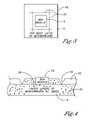
- FIG. 3is a top plan view of the motherboard with BGA module.
- FIG. 4is a side elevational view of an alternate motherboard with BGA module.
- a systemis shown, generally designated 10 , which includes a portable housing 12 and a computer motherboard 14 supported therein. While the system 10 shown in FIG. 1 is a portable computing device such as a laptop computer, wireless telephone, or the like, and while reference is made to the motherboard 14 for illustration, the principles advanced herein apply to non-portable computers that may nonetheless be subject to mechanical shock and to circuit boards other than motherboards. Also, while BGA modules are discussed below, present principles apply to modules that are subject to shock other than BGA modules.
- One or more ball grid array (BGA) modules 16are mounted to the motherboard 14 using the above-referenced solder balls 18 on the module 16 in accordance with principles known in the art.
- the BGA module 16 shown in FIG. 1may be any computer chip or other modular component that is mounted to the motherboard 14 using BGA mounting principles.
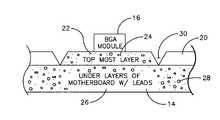
- FIG. 2shows that a topmost layer 20 is formed on the motherboard 14 .
- the layer 20is made of circuit board material.
- the volumetric regions 22 of the topmost layer 20 that lie under the intended location of a BGA modulecontain electrical leads 24 , for the purpose of electrically connecting the solder balls 18 ( FIG. 1 ) of the BGA module 16 to other components on the motherboard.
- Volumetric regions of the topmost layer 20 that lie outside the regions 22preferably do not contain electrical leads.
- the topmost layer 20is not formed in areas between the intended locations of BGA modules and the motherboard 14 , so that the BGA modules can be electrically connected to underlayers 26 of the motherboard 14 that contain electrical leads 28 . In this case, no region of the topmost layer 20 need contain electrical leads.
- V-shaped channels 30are formed (e.g., by cutting or molding) into the topmost layer 20 adjacent the BGA module 16 to impede mechanical stress from reaching the solder joints of the BGA module.
- each V-shaped channel 30defines opposed walls that are oblique to each other and that extend down toward each other through the topmost layer 20 .
- a dashed, perforation-like cutcan be used instead of a continuous V-shaped channel. In either case, a stress relied channel is formed.
- V-shaped channels 30preferably are formed between the BGA module 16 and each edge 32 of the motherboard 14 that borders the BGA module 16 . Indeed, it is preferred that no BGA module be closer to an edge 32 of the motherboard 14 than an intervening V-shaped channel 30 . In this way, mechanical stress that would otherwise propagate to solder joints that hold the BGA module 16 to the motherboard 14 is shielded from the solder joints by the V-shaped channels 30 .
- V-shaped channels 30may be formed along each motherboard edge 32 and parallel thereto, so that some V-shaped channels 30 are orthogonal to and may even cross other channels 30 .
Landscapes
- Engineering & Computer Science (AREA)
- Microelectronics & Electronic Packaging (AREA)
- Electric Connection Of Electric Components To Printed Circuits (AREA)
- Combinations Of Printed Boards (AREA)
Abstract
Description
Claims (14)
Priority Applications (2)
| Application Number | Priority Date | Filing Date | Title |
|---|---|---|---|
| US11/245,375US7492044B2 (en) | 2005-10-06 | 2005-10-06 | System and method for decreasing stress on solder holding BGA module to computer motherboard |
| CN200610159682.6ACN1946263B (en) | 2005-10-06 | 2006-09-30 | System and method for decreasing stress on circuit board and mobile processing device |
Applications Claiming Priority (1)
| Application Number | Priority Date | Filing Date | Title |
|---|---|---|---|
| US11/245,375US7492044B2 (en) | 2005-10-06 | 2005-10-06 | System and method for decreasing stress on solder holding BGA module to computer motherboard |
Publications (2)
| Publication Number | Publication Date |
|---|---|
| US20070090525A1 US20070090525A1 (en) | 2007-04-26 |
| US7492044B2true US7492044B2 (en) | 2009-02-17 |
Family
ID=37984592
Family Applications (1)
| Application Number | Title | Priority Date | Filing Date |
|---|---|---|---|
| US11/245,375Expired - Fee RelatedUS7492044B2 (en) | 2005-10-06 | 2005-10-06 | System and method for decreasing stress on solder holding BGA module to computer motherboard |
Country Status (2)
| Country | Link |
|---|---|
| US (1) | US7492044B2 (en) |
| CN (1) | CN1946263B (en) |
Cited By (1)
| Publication number | Priority date | Publication date | Assignee | Title |
|---|---|---|---|---|
| EP2448377A4 (en)* | 2009-06-25 | 2014-03-12 | Kyocera Corp | MULTIPLE PATTERN WIRING SUBSTRATE, WIRING SUBSTRATE, AND ELECTRONIC DEVICE |
Citations (18)
| Publication number | Priority date | Publication date | Assignee | Title |
|---|---|---|---|---|
| JPH04340794A (en) | 1991-05-17 | 1992-11-27 | Mitsubishi Electric Corp | printed wiring board |
| US5195023A (en)* | 1991-12-23 | 1993-03-16 | At&T Bell Laboratories | Integrated circuit package with strain relief grooves |
| JPH05335696A (en) | 1992-05-29 | 1993-12-17 | Nippon Mektron Ltd | Foldable flexible circuit board and manufacture thereof |
| EP0590429A2 (en) | 1992-09-28 | 1994-04-06 | The Whitaker Corporation | Edge connectors and contacts used therein |
| US5445240A (en) | 1994-08-04 | 1995-08-29 | Cunningham. Edward V. | Permanent magnet assembly |
| US5943597A (en)* | 1998-06-15 | 1999-08-24 | Motorola, Inc. | Bumped semiconductor device having a trench for stress relief |
| JP2001094000A (en) | 1999-09-21 | 2001-04-06 | Fuji Photo Film Co Ltd | Semiconductor device |
| US6325643B1 (en) | 1998-10-29 | 2001-12-04 | Ddk Ltd. | Press-in contact |
| US20020074147A1 (en) | 2000-12-15 | 2002-06-20 | Semiconductor Components Industries, Llc | Bump chip lead frame and package |
| US6426154B1 (en) | 1999-09-28 | 2002-07-30 | Kabushiki Kaisha Toshiba | Ceramic circuit board |
| US20030089969A1 (en)* | 1997-01-17 | 2003-05-15 | Seiko Epson Corporation | Electronic component, semiconductor device, methods of manufacturing the same, circuit board, and electronic instrument |
| US6682354B2 (en) | 2001-02-16 | 2004-01-27 | Ems Technologies, Inc. | Board edge launch connector |
| US20040070721A1 (en) | 2002-10-11 | 2004-04-15 | Masaki Tsubokura | Image display device |
| US6773269B1 (en) | 2002-09-27 | 2004-08-10 | Emc Corporation | Circuit board assembly which utilizes a pin assembly and techniques for making the same |
| US6927344B1 (en) | 2004-02-27 | 2005-08-09 | Motorola, Inc. | Flexible circuit board assembly |
| US6943502B2 (en) | 2000-06-12 | 2005-09-13 | Matsushita Electric Works, Ltd. | Electronic ballast for a discharge lamp |
| US6979595B1 (en)* | 2000-08-24 | 2005-12-27 | Micron Technology, Inc. | Packaged microelectronic devices with pressure release elements and methods for manufacturing and using such packaged microelectronic devices |
| US7285856B2 (en)* | 2003-05-30 | 2007-10-23 | Shinko Electric Industries Co., Ltd. | Package for semiconductor devices |
- 2005
- 2005-10-06USUS11/245,375patent/US7492044B2/ennot_activeExpired - Fee Related
- 2006
- 2006-09-30CNCN200610159682.6Apatent/CN1946263B/ennot_activeExpired - Fee Related
Patent Citations (21)
| Publication number | Priority date | Publication date | Assignee | Title |
|---|---|---|---|---|
| JPH04340794A (en) | 1991-05-17 | 1992-11-27 | Mitsubishi Electric Corp | printed wiring board |
| US5195023A (en)* | 1991-12-23 | 1993-03-16 | At&T Bell Laboratories | Integrated circuit package with strain relief grooves |
| JPH05335696A (en) | 1992-05-29 | 1993-12-17 | Nippon Mektron Ltd | Foldable flexible circuit board and manufacture thereof |
| EP0590429A2 (en) | 1992-09-28 | 1994-04-06 | The Whitaker Corporation | Edge connectors and contacts used therein |
| US5393234A (en) | 1992-09-28 | 1995-02-28 | The Whitaker Corporation | Edge connectors and contacts used therein |
| US5445240A (en) | 1994-08-04 | 1995-08-29 | Cunningham. Edward V. | Permanent magnet assembly |
| US20030089969A1 (en)* | 1997-01-17 | 2003-05-15 | Seiko Epson Corporation | Electronic component, semiconductor device, methods of manufacturing the same, circuit board, and electronic instrument |
| US5943597A (en)* | 1998-06-15 | 1999-08-24 | Motorola, Inc. | Bumped semiconductor device having a trench for stress relief |
| US6325643B1 (en) | 1998-10-29 | 2001-12-04 | Ddk Ltd. | Press-in contact |
| JP2001094000A (en) | 1999-09-21 | 2001-04-06 | Fuji Photo Film Co Ltd | Semiconductor device |
| US6426154B1 (en) | 1999-09-28 | 2002-07-30 | Kabushiki Kaisha Toshiba | Ceramic circuit board |
| US6943502B2 (en) | 2000-06-12 | 2005-09-13 | Matsushita Electric Works, Ltd. | Electronic ballast for a discharge lamp |
| US6979595B1 (en)* | 2000-08-24 | 2005-12-27 | Micron Technology, Inc. | Packaged microelectronic devices with pressure release elements and methods for manufacturing and using such packaged microelectronic devices |
| US20020074147A1 (en) | 2000-12-15 | 2002-06-20 | Semiconductor Components Industries, Llc | Bump chip lead frame and package |
| US6864423B2 (en) | 2000-12-15 | 2005-03-08 | Semiconductor Component Industries, L.L.C. | Bump chip lead frame and package |
| US6682354B2 (en) | 2001-02-16 | 2004-01-27 | Ems Technologies, Inc. | Board edge launch connector |
| US6773269B1 (en) | 2002-09-27 | 2004-08-10 | Emc Corporation | Circuit board assembly which utilizes a pin assembly and techniques for making the same |
| US20040070721A1 (en) | 2002-10-11 | 2004-04-15 | Masaki Tsubokura | Image display device |
| US7285856B2 (en)* | 2003-05-30 | 2007-10-23 | Shinko Electric Industries Co., Ltd. | Package for semiconductor devices |
| US6927344B1 (en) | 2004-02-27 | 2005-08-09 | Motorola, Inc. | Flexible circuit board assembly |
| US20050190531A1 (en) | 2004-02-27 | 2005-09-01 | Gall Thomas P. | Flexible circuit board assembly |
Non-Patent Citations (1)
| Title |
|---|
| "Motherboard". Oxford English Dictionary Online. Draft Revision Dec. 2002. Mar. 13, 2007. Keyword: motherboard. http://dictionary.oed.com/cgi/entry/00316365?single=1&query-type=word&word&queryword=mother-board&first=1&max-to-show=10.* |
Cited By (1)
| Publication number | Priority date | Publication date | Assignee | Title |
|---|---|---|---|---|
| EP2448377A4 (en)* | 2009-06-25 | 2014-03-12 | Kyocera Corp | MULTIPLE PATTERN WIRING SUBSTRATE, WIRING SUBSTRATE, AND ELECTRONIC DEVICE |
Also Published As
| Publication number | Publication date |
|---|---|
| US20070090525A1 (en) | 2007-04-26 |
| CN1946263A (en) | 2007-04-11 |
| CN1946263B (en) | 2014-10-01 |
Similar Documents
| Publication | Publication Date | Title |
|---|---|---|
| US10741951B2 (en) | Socket connector assembly for an electronic package | |
| JP5547818B2 (en) | Printed circuit board | |
| US7602615B2 (en) | In-grid decoupling for ball grid array (BGA) devices | |
| US20150022985A1 (en) | Device-embedded package substrate and semiconductor package including the same | |
| US11497122B2 (en) | Grid array connector system | |
| US9119320B2 (en) | System in package assembly | |
| US20130055192A1 (en) | Motherboard Assembly for Interconnecting and Distributing Signals and Power | |
| US7554189B1 (en) | Wireless communication module | |
| CN102280429A (en) | Circuit board, circuit board assembly, and semiconductor device | |
| WO2007029355A1 (en) | Shield structure | |
| US20190037707A1 (en) | Printed circuit board with edge soldering for high-density packages and assemblies | |
| EP2447994A2 (en) | Electronic component and electronic device | |
| US7492044B2 (en) | System and method for decreasing stress on solder holding BGA module to computer motherboard | |
| US9101058B2 (en) | IC package and assembly | |
| US20080042276A1 (en) | System and method for reducing stress-related damage to ball grid array assembly | |
| US20210298183A1 (en) | Buried electrical debug access port | |
| US20170068055A1 (en) | Optical module connector and printed board assembly | |
| US7180171B1 (en) | Single IC packaging solution for multi chip modules | |
| US8907490B2 (en) | Semiconductor packages having the first and second chip inclined sidewalls contact with each other | |
| US7812445B2 (en) | Semiconductor memory module having an oblique memory chip | |
| KR100590477B1 (en) | Memory module and motherboard connection structure using the edge of motherboard and memory module | |
| JP2005079387A (en) | Semiconductor device, semiconductor module, and semiconductor device manufacturing method | |
| JPWO2004112450A1 (en) | Substrate mounting method and mounting structure | |
| KR200444404Y1 (en) | USB memory device with antistatic function | |
| JP2000216298A (en) | Reinforcing structure of ic package |
Legal Events
| Date | Code | Title | Description |
|---|---|---|---|
| AS | Assignment | Owner name:LENOVO (SINGAPORE) PTE. LTD., SINGAPORE Free format text:ASSIGNMENT OF ASSIGNORS INTEREST;ASSIGNORS:LOCKER, HOWARD JEFFREY;CROMER, DARYL CARVIS;WONG, TIN-LUP;REEL/FRAME:016918/0397 Effective date:20051005 | |
| FEPP | Fee payment procedure | Free format text:PAYOR NUMBER ASSIGNED (ORIGINAL EVENT CODE: ASPN); ENTITY STATUS OF PATENT OWNER: LARGE ENTITY | |
| STCF | Information on status: patent grant | Free format text:PATENTED CASE | |
| FPAY | Fee payment | Year of fee payment:4 | |
| AS | Assignment | Owner name:LENOVO PC INTERNATIONAL, HONG KONG Free format text:NUNC PRO TUNC ASSIGNMENT;ASSIGNOR:LENOVO (SINGAPORE) PTE LTD.;REEL/FRAME:037160/0001 Effective date:20130401 | |
| FPAY | Fee payment | Year of fee payment:8 | |
| FEPP | Fee payment procedure | Free format text:MAINTENANCE FEE REMINDER MAILED (ORIGINAL EVENT CODE: REM.); ENTITY STATUS OF PATENT OWNER: LARGE ENTITY | |
| LAPS | Lapse for failure to pay maintenance fees | Free format text:PATENT EXPIRED FOR FAILURE TO PAY MAINTENANCE FEES (ORIGINAL EVENT CODE: EXP.); ENTITY STATUS OF PATENT OWNER: LARGE ENTITY | |
| STCH | Information on status: patent discontinuation | Free format text:PATENT EXPIRED DUE TO NONPAYMENT OF MAINTENANCE FEES UNDER 37 CFR 1.362 | |
| FP | Lapsed due to failure to pay maintenance fee | Effective date:20210217 |