US7492027B2 - Reduced crosstalk sensor and method of formation - Google Patents
Reduced crosstalk sensor and method of formationDownload PDFInfo
- Publication number
- US7492027B2 US7492027B2US10/781,706US78170604AUS7492027B2US 7492027 B2US7492027 B2US 7492027B2US 78170604 AUS78170604 AUS 78170604AUS 7492027 B2US7492027 B2US 7492027B2
- Authority
- US
- United States
- Prior art keywords
- trench
- sensor
- oxide
- dielectric
- sidewalls
- Prior art date
- Legal status (The legal status is an assumption and is not a legal conclusion. Google has not performed a legal analysis and makes no representation as to the accuracy of the status listed.)
- Ceased, expires
Links
Images


Classifications
- H—ELECTRICITY
- H10—SEMICONDUCTOR DEVICES; ELECTRIC SOLID-STATE DEVICES NOT OTHERWISE PROVIDED FOR
- H10F—INORGANIC SEMICONDUCTOR DEVICES SENSITIVE TO INFRARED RADIATION, LIGHT, ELECTROMAGNETIC RADIATION OF SHORTER WAVELENGTH OR CORPUSCULAR RADIATION
- H10F99/00—Subject matter not provided for in other groups of this subclass
- H—ELECTRICITY
- H10—SEMICONDUCTOR DEVICES; ELECTRIC SOLID-STATE DEVICES NOT OTHERWISE PROVIDED FOR
- H10F—INORGANIC SEMICONDUCTOR DEVICES SENSITIVE TO INFRARED RADIATION, LIGHT, ELECTROMAGNETIC RADIATION OF SHORTER WAVELENGTH OR CORPUSCULAR RADIATION
- H10F39/00—Integrated devices, or assemblies of multiple devices, comprising at least one element covered by group H10F30/00, e.g. radiation detectors comprising photodiode arrays
- H10F39/80—Constructional details of image sensors
- H10F39/807—Pixel isolation structures
- H—ELECTRICITY
- H10—SEMICONDUCTOR DEVICES; ELECTRIC SOLID-STATE DEVICES NOT OTHERWISE PROVIDED FOR
- H10F—INORGANIC SEMICONDUCTOR DEVICES SENSITIVE TO INFRARED RADIATION, LIGHT, ELECTROMAGNETIC RADIATION OF SHORTER WAVELENGTH OR CORPUSCULAR RADIATION
- H10F39/00—Integrated devices, or assemblies of multiple devices, comprising at least one element covered by group H10F30/00, e.g. radiation detectors comprising photodiode arrays
- H10F39/011—Manufacture or treatment of image sensors covered by group H10F39/12
- H10F39/014—Manufacture or treatment of image sensors covered by group H10F39/12 of CMOS image sensors
- H—ELECTRICITY
- H10—SEMICONDUCTOR DEVICES; ELECTRIC SOLID-STATE DEVICES NOT OTHERWISE PROVIDED FOR
- H10F—INORGANIC SEMICONDUCTOR DEVICES SENSITIVE TO INFRARED RADIATION, LIGHT, ELECTROMAGNETIC RADIATION OF SHORTER WAVELENGTH OR CORPUSCULAR RADIATION
- H10F39/00—Integrated devices, or assemblies of multiple devices, comprising at least one element covered by group H10F30/00, e.g. radiation detectors comprising photodiode arrays
- H10F39/10—Integrated devices
- H10F39/12—Image sensors
- H10F39/18—Complementary metal-oxide-semiconductor [CMOS] image sensors; Photodiode array image sensors
- H10F39/182—Colour image sensors
- H—ELECTRICITY
- H10—SEMICONDUCTOR DEVICES; ELECTRIC SOLID-STATE DEVICES NOT OTHERWISE PROVIDED FOR
- H10F—INORGANIC SEMICONDUCTOR DEVICES SENSITIVE TO INFRARED RADIATION, LIGHT, ELECTROMAGNETIC RADIATION OF SHORTER WAVELENGTH OR CORPUSCULAR RADIATION
- H10F39/00—Integrated devices, or assemblies of multiple devices, comprising at least one element covered by group H10F30/00, e.g. radiation detectors comprising photodiode arrays
- H10F39/80—Constructional details of image sensors
- H10F39/803—Pixels having integrated switching, control, storage or amplification elements
Definitions
- the present inventionrelates generally to semiconductor devices, and more particularly, to trench isolation technology for use in semiconductor devices, including CMOS image sensors.
- CMOS imagersare increasingly being used as low cost imaging devices over charge coupled devices (CCD).
- a CMOS image sensor circuitincludes a focal plane array of pixel cells, each one of the cells including a photo-conversion device for generating and accumulating charge in response to light incident on the pixel cell.
- Each pixel cellalso includes devices, e.g., transistors, for transferring charge from the photo-conversion device to readout circuitry for readout.
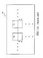
- FIGS. 1A-1Bdepict two adjacent conventional CMOS pixel cells 100 a , 100 b of an array 199 .
- FIG. 1Ais a top plan view of the pixel cells and FIG. 1B is a cross-sectional view of the pixel cells of FIG. 1A along line 1 B- 1 B′.
- Pixel cells 100 a , 100 bare formed at a surface of a substrate 101 .
- Substrate 101is a p-type substrate overlying a heavily doped p-type substrate base 102 .
- Each pixel cell 100 a , 100 bincludes a photo-conversion device, which is depicted as a pinned photodiode 110 a , 110 b .
- the pinned photodiodes 110 a , 110 brespectively include a doped p-type surface layer 111 a , 111 b overlying a doped n-type region 112 a , 112 b .
- the n-type regionsserve to accumulate charge carriers, e.g., electrons, that are generated by photons of light incident on pinned photodiodes 110 a , 110 b and absorbed within substrate 101 .
- sensing nodeswhich are depicted as floating diffusion nodes 116 a , 116 b on opposite sides of a respective transfer gate 115 a , 115 b to pinned photodiode 110 .
- Floating diffusion nodes 116 a , 116 bare doped n-type regions and receive charge transferred from the pinned photodiodes 110 a , 110 b by the respective transfer gates 115 a , 115 b.
- each pixel cell 100 a , 100 balso includes a respective reset transistor for resetting their floating diffusion regions 116 a , 116 b to a predetermined voltage before sensing a signal; and a row select transistor for outputting a signal from a source follower transistor to an output terminal in response to an address signal.
- CMOS image sensors of the type discussed aboveare generally known as discussed, for example, in Nixon et al., 256 ⁇ 256 CMOS Active Pixel Sensor Camera - on - a - Chip , IEEE Journal of Solid-State Circuits, Vol. 31(12), pp.
- Adjacent pixel cells 100 a , 100 b , and/or other pixel cells (not shown) of array 199can interfere with each another causing crosstalk, which results in poor image quality.
- Crosstalkcan be either optical or electrical. Isolation techniques have been used to prevent crosstalk between pixel cells. This disclosure concerns electrical isolation techniques to prevent crosstalk. Electrical isolation is complex and depends on a number of factors including photon absorption in the substrate 101 , photon wavelength, characteristics of the pinned photodiodes 110 a , 110 b the life-time of minority carriers, and generation and recombination centers in the substrate 101 , among others.
- Shallow trench isolationis one electrical isolation technique, which has been used to isolate pixels cells, as well as devices or circuitry, from one other.
- a trench 120 a , 120 bis etched into the substrate 101 and filled with a dielectric to provide a physical and electrical barrier between adjacent pixels ( 100 a , 110 b ), devices, or circuitry.
- the depth of an STI regionis generally from about 2000 Angstroms ( ⁇ ) to about 2500 ⁇ .
- STIOne drawback associated with STI is crosstalk from a photon that is absorbed deep within the substrate 101 of pinned photodiodes 110 a , 110 b .
- Table 1shows the absorption depth for photons of different wavelengths in a silicon substrate.
- pinned photodiodes 110 a , 110 bmust have a deeper p-n junction depth to capture the long wavelength photons.
- the absorption depthsare high and photons travel far into the substrate 101 before being absorbed and generate charge carriers. Therefore, electrons generated by such photons must travel long distances before reaching the floating diffusion region. Accordingly, there is a greater chance that such electrons will travel to other pixel cells, causing crosstalk between adjacent pixels.
- FIG. 1Ais a top plan view of two pixels of a CMOS pixel cell
- FIG. 1Bis a cross sectional view of the pixel cell of FIG. 1A ;
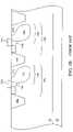
- FIG. 2is a cross sectional view of a trench according to a first exemplary embodiment of the invention
- FIG. 3Ais a cross sectional view of the pixel cells of FIG. 2A at an intermediate stage of processing
- FIG. 3Bis a cross sectional view of the pixel cells of FIG. 2A at an intermediate stage of processing
- FIG. 3Cis a cross sectional view of the pixel cells of FIG. 2A at an intermediate stage of processing
- FIG. 4is a cross sectional view of a trench according to a second exemplary embodiment of the invention.
- FIG. 5is a cross sectional view of a trench according to a third exemplary embodiment of the invention.
- FIG. 6is a cross sectional view of a trench according to a fourth exemplary embodiment of the invention.
- FIG. 7illustrates a trench of the present invention surrounding red pixels of a Bayer pattern
- FIG. 8is a schematic diagram of a processor system incorporating an exemplary embodiment of the invention.
- wafer and substrateare to be understood as including silicon, silicon-on-insulator (SOI), or silicon-on-sapphire (SOS) technology, doped and undoped semiconductors, epitaxial layers of silicon supported by a base semiconductor foundation, and other semiconductor structures.
- SOIsilicon-on-insulator
- SOSsilicon-on-sapphire
- doped and undoped semiconductorsdoped and undoped semiconductors
- epitaxial layers of silicon supported by a base semiconductor foundationand other semiconductor structures.
- previous process stepsmay have been utilized to form regions or junctions in the base semiconductor structure or foundation.
- the semiconductorneed not be silicon-based, but could be based on silicon-germanium, germanium, or gallium-arsenide.
- pixelrefers to a picture element unit cell having an active area and containing a photo-conversion device and other devices, e.g., transistors, for converting electromagnetic radiation to an electrical signal.
- a representative pixel cellsare illustrated in the Figure s and description herein, and typically fabrication of all pixels in an image sensor will proceed simultaneously in a similar fashion.
- CMOS image sensorFor simplicity, exemplary embodiments described herein are explained with reference to a CMOS image sensor. However, it should be noted that the invention is not limited to CMOS image sensors and may be used in any suitable device, for example, a charge coupled device (CCD) image sensor.
- CCDcharge coupled device
- Shallow trench isolation regions for CMOS image sensorsgenerally have a depth of less than about 3000 Angstroms ( ⁇ ) and are generally around about 2000 ⁇ to about 2500 ⁇ .
- STI regionsare filled with a conventional insulator, such as oxides or high density plasma (HDP) oxides.
- a conventional insulatorsuch as oxides or high density plasma (HDP) oxides.
- HDPhigh density plasma
- the width (W)may vary, but is preferably shorter than the depth (D) of the trench.
- a trench 202is preferably filled with conductive materials containing silicon, preferably polysilicon or silicon-germanium.
- Conductive materials containing siliconmay be easily deposited into trenches of various depths, unlike conventional insulation materials, e.g., silicon dioxide, silicon nitride, NO, ON, HDP, and ONO, which are difficult to fill in deep trenches.
- a conductive material containing silicon, or a combination of such conductive materials containing siliconto fill the trench 202 allows easy formation of a trench, particularly, a deep trench having a depth (D) greater than about 2000 ⁇ , and preferably about 4000 to about 5000 ⁇ .
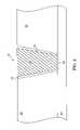
- the trench 202should extend to the epi layer 201 as shown in FIG. 2
- a trench according to the inventionis deeper than a shallow trench, and accordingly has longer sidewalls than a shallow trench. Therefore, the longer sidewalls allow for a larger electrical connection region 323 along the sidewalls of the trench 202 such that electron storage capacitance, e.g., hole accumulation, in the electrical connection region 323 is increased in accordance with the invention.
- a trench in accordance with the inventionprovides improved isolation between pixels.
- the deeper trenchbetter inhibits electrons from diffusing under the isolation trench to an adjacent pixel thereby preventing crosstalk between neighboring pixels.
- the deeper trenchallows for tighter isolation design rules. Deeper trenches may also be narrower than shallow trenches, while still providing effective isolation between neighboring regions. Accordingly, the source/drain regions of one pixel may be brought closer to the active layer of an adjacent pixel, by narrowing the width of the deep trench.
- a trench 202is etched into substrate 200 , which is adjacent to photodiode region 203 .
- the trench 202preferably extends near, or directly above base layer 201 .
- An anisotropic etchis performed into the silicon substrate 200 to create a deep trench 202 .
- a resist and maskare applied, and photolithographic techniques are used to define the area to be etched-out of substrate 200 .
- a directional etching process, such as Reactive Ion Etching (RIE), or etching with a preferential anisotropic etchantis used to etch into a doped active layer to form the trench 202 .
- the resist and maskare removed leaving a structure that appears as shown in FIG. 3A .
- an oxidei.e., silicon oxide, silicon dioxide or other dielectric liner 204
- the linermay be formed by known techniques and may be a high density plasma (HDP) oxide, a spin on dielectric (SOD), e.g., silicon oxide, or other suitable material.
- Liner 204can be substantially conformal such that the thickness of the liner 204 is substantially the same along the sidewalls 210 and at the bottom 220 of the trench 202 . In general, the thickness of the dielectric liner 204 along the sidewalls 210 should be at least about 100 Angstroms. Alternatively, a direct deposit of an insulator could be performed.
- part of the trenchmay be filled with disposable, doped oxide material after the trench etch to create a film over the trench.
- the disposable oxide filmmay be boron-doped BSG, or phosphor-doped PSG, or other suitable material.
- a HF dipwill remove part of the film from the top of the trench, leaving film only along the sidewalls and bottom of the trench.
- a short anneal processthen follows to out-diffuse dopants from the film to the sidewalls of the trench.
- the boron-doped BSGacts as a solid-source diffusion source for boron.
- a high concentration boron doped regionwill be formed near the sidewall and the bottom of the trench. This high-doped region will serve to connect the top surface p-layer 203 to the bottom p-substrate epi layer 201 in a pinned photodiode structure. Also, high conical sidewalls without the use of high dose implants can create a good interface without defects for reduced dark current.
- a highly doped (in-situ doped) n-type or p-type conductive material containing silicon 205is deposited to fill the trench 202 .
- Suitable conductive materials containing siliconinclude polysilicon and silicon-germanium.
- the trench 202may be filled with an undoped conductive material containing silicon, which can remain free of dopants or be subsequently implanted with dopants.
- a masked ion implantmay be performed to dope the conductive material containing silicon.
- p-type ionssuch as boron (B) can be implanted into the conductive material 205 containing silicon using a photoresist mask.
- the depth of the trenchcan be tailored to extend to the surface of epi layer 201 .
- the starting epi thicknessis 4 ⁇ m deep
- a trench having a depth of 3 ⁇ mwould help to connect the buried p or n epi layer 201 to the upper surface p or n layer 203 after it diffuses out 1.5 ⁇ m towards the surface during the processing steps described above.
- a much deeper trenche.g., 8 ⁇ m may be used for such applications as infra-red, or near infra-red sensors.
- FIG. 4illustrates yet another embodiment of the present invention, according to which trench 302 is lined with an oxide or dielectric liner 304 only on the sidewalls of the trench, and not on its bottom.
- the material filling the trench 302for example, highly doped polysilicon, directly contacts the epi layer 201 located beneath the trench, providing a hookup area to the substrate 200 .
- the two sidewall STI layersisolate adjacent pixels and provide better scaling.
- the trench 302is etched into substrate 200 , which is adjacent to photodiode region 203 .
- the trench 202preferably extends near, or directly above base layer 201 .
- An anisotropic etchis performed into the silicon substrate 200 to create a deep trench.
- a resist and maskare applied, and photolithographic techniques are used to define the area to be etched-out of substrate 200 .
- a directional etching processsuch as Reactive Ion Etching (RIE), or etching with a preferential anisotropic etchant is used to etch into a doped active layer to form the trench 302 .
- RIEReactive Ion Etching
- An oxide, such as silicon oxide, silicon dioxide or other dielectric liner 304is grown or deposited on sidewalls 310 but not on bottom 320 of trench 302 , as also shown in FIG. 4 .
- the formation of the dielectric liner 304 only on sidewalls 310may be accomplished, for example, by masking the bottom 320 of the trench 302 and then forming the dielectric liner 304 on the sidewalls 310 .
- the dielectric liner 304may be first formed within the trench 302 , on both the sidewalls 310 and the bottom 320 , and then removed from the bottom 320 .
- Liner 304may be formed by known techniques and may be a high density plasma (HDP) oxide, a spin on dielectric (SOD), e.g., silicon oxide, or other suitable material. In general, the thickness of the dielectric liner 304 along the sidewalls 310 should be at least about 100 Angstroms.
- HDPhigh density plasma
- SODspin on dielectric
- a highly doped (in-situ doped) n-type or p-type conductive material containing silicon 305is next deposited to fill the trench 302 .
- Suitable conductive materials containing siliconinclude polysilicon and silicon-germanium.
- the trench 302may be filled with an undoped conductive material containing silicon, which can remain free of dopants or be subsequently implanted with dopants.
- a masked ion implantmay be performed to dope the conductive material containing silicon.
- p-type ionssuch as boron (B) can be implanted into the conductive material 305 containing silicon using a photoresist mask.
- FIG. 5illustrates yet another embodiment of the present invention, according to which trench 402 incorporates a plurality of dielectric films, at least two of each having different refractive indices.
- FIG. 5depicts trench 402 containing three materials 410 , 420 and 430 having different refractive indices. Based on the refractive indices, the layering structure of materials 410 , 420 and 430 is configured so that photons entering the trench 402 from adjacent circuitry will be reflected away from the photodiode region 203 .
- material 410has a greater refractive index that that of material 420 , which in turn has a greater refractive index than that of material 430 .
- the materials having different refractive indicesmay comprise any dielectric material, such as undoped polysilicon, silicon dioxide, aluminum dioxide, spin-on-dielectric (SOD), silicon nitride, or any combination of these dielectric materials.
- dielectric materialsuch as undoped polysilicon, silicon dioxide, aluminum dioxide, spin-on-dielectric (SOD), silicon nitride, or any combination of these dielectric materials.
- PE-oxidePECVD oxide
- FSG-oxidefluorinated silica glass oxide
- PE-oxide and FSG-oxide multiple layersmay be also used as combinations of materials with different refractive indices to fill in trench 402 .
- the PE-oxide/FSG-oxide combination for improving optical crosstalk above the silicon active area of a CMOS image sensoris disclosed, for example, by Hsu et al. in Light Guide for Pixel Crosstalk Improvement, Deep Submicron CMOS Image Sensor , IEEE Vol. 25, No. 1 (January 2004), the disclosure of which is incorporated by reference herein.
- the total internal reflection (TIR)is minimized so that the photons that would otherwise get lost are confined and they bounce off an interface that has refractive index difference between the two materials. This, in turn, allows an increase in the quantum efficiency of the array.
- FIG. 6illustrates yet another embodiment of the present invention.
- a contact 500is dropped to the conductive material 205 of trench 502 so that any trapped charge into the conductive material 205 may be efficiently removed.
- the trench 502is similar to the trench 202 of FIGS. 3A-3B and is formed by a process similar to that for the formation of the trench 202 .
- the difference between the trenches 502 and 202is that the trench 502 has contact 500 to the conductive material 205 inside of the trench 502 .
- Providing contact 500may be accomplished by strapping the conductive material 205 (for example, highly doped polysilicon or undoped conductive material containing silicon) in the array together and dropping a contact in the edge of the array.
- the conductive material 205for example, highly doped polysilicon or undoped conductive material containing silicon
- this biascan be adjusted to create an accumulation region around the sidewalls of the STI. By doing so, it is possible to reduce or eliminate the need for doping the sidewall region.
- the sidewallhas to be p-type to hookup to the substrate.
- the conductive material 205 inside of the trench 502is n+ polysilicon, this material can be biased negatively to create a hole-rich accumulation region on the sidewalls 210 of the trench 502 .
- the conductive material 205 inside of the trench 502is p+ polysilicon, then the p+ polysilicon would be biased positively.
- the biasmay be in the range of about 100 to 500 mV in absolute value.
- the bias conditionswould be reversed to create an electron-rich accumulation region on the sidewalls 210 of the trench 502 .
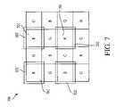
- FIG. 7illustrate an exemplary application of the deep trench isolation structures of the present invention to a color filter array 700 for capturing images in a digital camera, for example.
- the color filter array 700comprises a plurality of deep trench isolation structures, such as the deep trench isolation structures 202 of FIGS. 3A-3C , for example, provided around the perimeter of predefined pixels 701 covered by corresponding color filters.
- the color filter array 700 of the present inventioncomprises deep trench isolation structures 202 surrounding red pixels 701 of a color filter array Bayer pattern.
- the deep trench isolation structures of the present inventionmay be used for isolating pixel cells of any known color filter array, and thus the invention is not limited to a Bayer color filter array.
- a Bayer patterncomprises pixels which are represented by squares in the grid of FIG. 7 .
- Each pixelincludes an electronic sensor which measures the light falling on it.
- Pixels 701have a red filter to measure red light and are represented by an R in the pattern.
- the Bayer patternis replicated throughout the entire color filter array in both the horizontal and vertical directions. By providing deep trenches around the red pixels of a color filter array, such as the Bayer color filter array of FIG. 7 , crosstalk between the red pixels (which have a deeper photon absorption than the green and blue pixels) is decreased and the image quality is accordingly increased.
- the deep trench isolation structureshave been illustrated in FIG. 7 as completely surrounding the red pixels 701 of a Bayer color filter array, it must be understood that this embodiment is only exemplary. As such, the present invention also contemplates the formation of deep trench isolation structures, such as the deep trench isolation structures 202 , 302 , 402 , 502 of the present invention, only partially surrounding red pixels of a color filter array, such as the red pixels 701 of the Bayer pattern of FIG. 7 . In addition, the deep trench isolation structures of the present invention may be formed surrounding totally or partially other pixels of a color filter array, for example the green pixels, or a combination of the red, green and blue pixels of a color array, as desired.
- a processor based system 600which includes a CMOS image sensor 642 according to the invention is illustrated in FIG. 8 .
- Processor based system 600is exemplary of a system having digital circuits, which could include an image sensor. Without being limiting, such a system could include a computer system, camera system, scanner, machine vision, vehicle navigation, video phone, surveillance system, auto focus system, star tracker system, motion detection system, image stabilization system and data compression system for high-definition television, all of which can utilize the present invention.
- Processor based system 600such as a computer system, for example generally comprises a central processing unit (CPU) 644 , for example, a microprocessor, which communicates with an input/output (I/O) device 646 over a bus 652 .
- the CMOS image sensor 642also includes an IC with a single or multiple isolation trench structures such as the deep trench isolation structures 202 , 302 , 402 , 502 of the present invention.
- the CMOS image sensor 642also communicates with components of the system 600 over bus 652 .
- the computer system 600also includes random access memory (RAM) 648 , and, in the case of a computer system may include peripheral devices such as a flash memory card 654 , or a compact disk (CD) ROM drive 656 , which also communicate with CPU 644 over the bus 652 . It may also be desirable to integrate the processor 654 , CMOS image sensor 642 and memory 648 on a single IC chip.
- RAMrandom access memory
- peripheral devicessuch as a flash memory card 654 , or a compact disk (CD) ROM drive 656 , which also communicate with CPU 644 over the bus 652 . It may also be desirable to integrate the processor 654 , CMOS image sensor 642 and memory 648 on a single IC chip.
- the inventionis not limited to these embodiments.
- the inventionalso has applicability to other types of photodiodes and to photodiodes formed from npn regions in a substrate. If an NPN-type photodiode is formed the dopant and conductivity types of all structures would change accordingly.
Landscapes
- Solid State Image Pick-Up Elements (AREA)
- Physics & Mathematics (AREA)
- Condensed Matter Physics & Semiconductors (AREA)
- Electromagnetism (AREA)
- General Physics & Mathematics (AREA)
Abstract
Description
| TABLE 1 | |||
| Wavelength (Nanometers) | Absorption Depth (Microns) | ||
| 400 | 0.19 | ||
| 450 | 1.0 | ||
| 500 | 2.3 | ||
| 550 | 3.3 | ||
| 600 | 5.0 | ||
| 650 | 7.6 | ||
| 700 | 8.5 | ||
| 750 | 16 | ||
| 800 | 23 | ||
| 850 | 46 | ||
| 900 | 62 | ||
| 950 | 150 | ||
| 1000 | 470 | ||
| 1050 | 1500 | ||
| 1100 | 7600 | ||
Claims (39)
Priority Applications (3)
| Application Number | Priority Date | Filing Date | Title |
|---|---|---|---|
| US10/781,706US7492027B2 (en) | 2004-02-20 | 2004-02-20 | Reduced crosstalk sensor and method of formation |
| US11/247,195US20060038252A1 (en) | 2004-02-20 | 2005-10-12 | Reduced crosstalk sensor and method of formation |
| US13/029,965USRE45633E1 (en) | 2004-02-20 | 2011-02-17 | Reduced crosstalk sensor and method of formation |
Applications Claiming Priority (1)
| Application Number | Priority Date | Filing Date | Title |
|---|---|---|---|
| US10/781,706US7492027B2 (en) | 2004-02-20 | 2004-02-20 | Reduced crosstalk sensor and method of formation |
Related Child Applications (2)
| Application Number | Title | Priority Date | Filing Date |
|---|---|---|---|
| US11/247,195DivisionUS20060038252A1 (en) | 2004-02-20 | 2005-10-12 | Reduced crosstalk sensor and method of formation |
| US13/029,965ReissueUSRE45633E1 (en) | 2004-02-20 | 2011-02-17 | Reduced crosstalk sensor and method of formation |
Publications (2)
| Publication Number | Publication Date |
|---|---|
| US20050184353A1 US20050184353A1 (en) | 2005-08-25 |
| US7492027B2true US7492027B2 (en) | 2009-02-17 |
Family
ID=34860920
Family Applications (3)
| Application Number | Title | Priority Date | Filing Date |
|---|---|---|---|
| US10/781,706CeasedUS7492027B2 (en) | 2004-02-20 | 2004-02-20 | Reduced crosstalk sensor and method of formation |
| US11/247,195AbandonedUS20060038252A1 (en) | 2004-02-20 | 2005-10-12 | Reduced crosstalk sensor and method of formation |
| US13/029,965Expired - LifetimeUSRE45633E1 (en) | 2004-02-20 | 2011-02-17 | Reduced crosstalk sensor and method of formation |
Family Applications After (2)
| Application Number | Title | Priority Date | Filing Date |
|---|---|---|---|
| US11/247,195AbandonedUS20060038252A1 (en) | 2004-02-20 | 2005-10-12 | Reduced crosstalk sensor and method of formation |
| US13/029,965Expired - LifetimeUSRE45633E1 (en) | 2004-02-20 | 2011-02-17 | Reduced crosstalk sensor and method of formation |
Country Status (1)
| Country | Link |
|---|---|
| US (3) | US7492027B2 (en) |
Cited By (15)
| Publication number | Priority date | Publication date | Assignee | Title |
|---|---|---|---|---|
| US20080105906A1 (en)* | 2004-07-07 | 2008-05-08 | Mitsuyoshi Mori | Solid State Imaging Apparatus Method for Fabricating the Same and Camera Using the Same |
| US20080124829A1 (en)* | 2004-12-09 | 2008-05-29 | Taiwan Semiconductor Manufacturing Co., Ltd. | Method for forming pinned photodiode resistant to electrical leakage |
| US20100270636A1 (en)* | 2009-04-23 | 2010-10-28 | Taiwan Semiconductor Manufacturing Company, Ltd. | Isolation structure for backside illuminated image sensor |
| US20110096208A1 (en)* | 2009-10-22 | 2011-04-28 | Stmicroelectronics (Crolles 2) Sas | Image sensor with vertical transfer gate |
| US20120001234A1 (en)* | 2010-07-05 | 2012-01-05 | Lim Sung-Won | Image sensor and method for fabricating the same |
| US8507962B2 (en) | 2010-10-04 | 2013-08-13 | International Business Machines Corporation | Isolation structures for global shutter imager pixel, methods of manufacture and design structures |
| US20130321685A1 (en)* | 2012-05-31 | 2013-12-05 | Samsung Electronics Co., Ltd. | Unit pixel of image sensor and pixel array including the unit pixel |
| US20150155327A1 (en)* | 2013-11-29 | 2015-06-04 | Sony Corporation | Solid-state imaging element, manufacturing method, and electronic device |
| US9508769B1 (en)* | 2016-02-01 | 2016-11-29 | Taiwan Semiconductor Manufacturing Company Ltd. | Semiconductor structure and method of manufacturing the same |
| US9584744B2 (en) | 2015-06-23 | 2017-02-28 | Semiconductor Components Industries, Llc | Image sensors with voltage-biased trench isolation structures |
| US9609250B2 (en) | 2014-08-19 | 2017-03-28 | Samsung Electronics Co., Ltd. | Unit pixels for image sensors and pixel arrays comprising the same |
| US20170207270A1 (en)* | 2016-01-15 | 2017-07-20 | Semiconductor Manufacturing International (Shanghai) Corporation | Method of manufacturing a cmos image sensor |
| US9748299B2 (en) | 2014-08-06 | 2017-08-29 | Samsung Electronics Co., Ltd. | Pixel, image sensor including the same, and portable electronic device including the image sensor |
| US10134792B2 (en) | 2016-08-25 | 2018-11-20 | Samsung Electronics Co., Ltd. | Semiconductor devices |
| US11791367B2 (en)* | 2019-12-02 | 2023-10-17 | Wuhan Xinxin Semiconductor Manufacturing Co., Ltd. | Semiconductor device and method of fabricating the same |
Families Citing this family (57)
| Publication number | Priority date | Publication date | Assignee | Title |
|---|---|---|---|---|
| US7442629B2 (en) | 2004-09-24 | 2008-10-28 | President & Fellows Of Harvard College | Femtosecond laser-induced formation of submicrometer spikes on a semiconductor substrate |
| US7057256B2 (en) | 2001-05-25 | 2006-06-06 | President & Fellows Of Harvard College | Silicon-based visible and near-infrared optoelectric devices |
| US7492027B2 (en) | 2004-02-20 | 2009-02-17 | Micron Technology, Inc. | Reduced crosstalk sensor and method of formation |
| US7154136B2 (en)* | 2004-02-20 | 2006-12-26 | Micron Technology, Inc. | Isolation structures for preventing photons and carriers from reaching active areas and methods of formation |
| FR2894072A1 (en)* | 2005-11-30 | 2007-06-01 | St Microelectronics Sa | Integrated circuit, e.g. optical detector, has inner volumes having surfaces on side of photosensitive element and lateral surfaces, respectively, where one of former surfaces has area smaller than area of one of lateral surface |
| KR100761829B1 (en)* | 2005-12-15 | 2007-09-28 | 삼성전자주식회사 | Semiconductor Device, CMOS Image Sensor, Manufacturing Method of Semiconductor Device and Manufacturing Method of CMOS Image Sensor |
| KR100790225B1 (en) | 2005-12-26 | 2008-01-02 | 매그나칩 반도체 유한회사 | Image sensor and its manufacturing method |
| US7982284B2 (en)* | 2006-06-28 | 2011-07-19 | Infineon Technologies Ag | Semiconductor component including an isolation structure and a contact to the substrate |
| US8071416B2 (en)* | 2006-08-17 | 2011-12-06 | Micron Technology, Inc. | Method of forming a uniform color filter array |
| US7973271B2 (en)* | 2006-12-08 | 2011-07-05 | Sony Corporation | Solid-state image pickup device, method for manufacturing solid-state image pickup device, and camera |
| KR100869743B1 (en)* | 2006-12-29 | 2008-11-21 | 동부일렉트로닉스 주식회사 | CMOS image sensor and its manufacturing method |
| JP5164509B2 (en)* | 2007-10-03 | 2013-03-21 | キヤノン株式会社 | Photoelectric conversion device, photoelectric conversion device for visible light, and imaging system using them |
| WO2009087533A1 (en)* | 2008-01-04 | 2009-07-16 | Nxp B.V. | Optical and electrical isolation of imager pixels and method for its fabrication |
| WO2009105120A1 (en)* | 2008-02-19 | 2009-08-27 | Sarnoff Corporation | Method and device for reducing crosstalk in back illuminated imagers |
| FR2930676B1 (en)* | 2008-04-24 | 2011-07-22 | St Microelectronics Crolles 2 | IMAGE SENSOR WITH VERY LOW DIMENSIONS |
| KR20100057302A (en)* | 2008-11-21 | 2010-05-31 | 삼성전자주식회사 | Image sensor and method for manufacturing thereof |
| US20100148230A1 (en)* | 2008-12-11 | 2010-06-17 | Stevens Eric G | Trench isolation regions in image sensors |
| KR101776955B1 (en)* | 2009-02-10 | 2017-09-08 | 소니 주식회사 | Solid-state imaging device, method of manufacturing the same, and electronic apparatus |
| US8133774B2 (en) | 2009-03-26 | 2012-03-13 | International Business Machines Corporation | SOI radio frequency switch with enhanced electrical isolation |
| US7923799B2 (en)* | 2009-06-09 | 2011-04-12 | Aptina Imaging Corporation | Image sensors with light guides |
| US8558336B2 (en)* | 2009-08-17 | 2013-10-15 | United Microelectronics Corp. | Semiconductor photodetector structure and the fabrication method thereof |
| JP5172819B2 (en)* | 2009-12-28 | 2013-03-27 | 株式会社東芝 | Solid-state imaging device |
| US8692198B2 (en) | 2010-04-21 | 2014-04-08 | Sionyx, Inc. | Photosensitive imaging devices and associated methods |
| WO2011160130A2 (en) | 2010-06-18 | 2011-12-22 | Sionyx, Inc | High speed photosensitive devices and associated methods |
| JP5726005B2 (en)* | 2010-08-02 | 2015-05-27 | アイメックImec | Method for manufacturing CMOS imaging device array |
| US8987841B2 (en) | 2010-08-09 | 2015-03-24 | Omnivision Technologies, Inc. | Backside stimulated sensor with background current manipulation |
| US8519490B2 (en)* | 2010-08-09 | 2013-08-27 | Omnivision Technologies, Inc. | Backside stimulated sensor with background current manipulation |
| FR2969385A1 (en) | 2010-12-21 | 2012-06-22 | St Microelectronics Crolles 2 | IMAGE SENSOR WITH REDUCED INTERMODULATION RATE |
| FR2969384A1 (en) | 2010-12-21 | 2012-06-22 | St Microelectronics Sa | IMAGE SENSOR WITH REDUCED INTERMODULATION |
| US8542311B2 (en) | 2011-01-20 | 2013-09-24 | Aptina Imaging Corporation | Multisection light guides for image sensor pixels |
| JP6299058B2 (en)* | 2011-03-02 | 2018-03-28 | ソニー株式会社 | Solid-state imaging device, method for manufacturing solid-state imaging device, and electronic apparatus |
| US9496308B2 (en) | 2011-06-09 | 2016-11-15 | Sionyx, Llc | Process module for increasing the response of backside illuminated photosensitive imagers and associated methods |
| WO2013010127A2 (en) | 2011-07-13 | 2013-01-17 | Sionyx, Inc. | Biometric imaging devices and associated methods |
| US8853811B2 (en)* | 2011-11-07 | 2014-10-07 | Taiwan Semiconductor Manufacturing Company, Ltd. | Image sensor trench isolation with conformal doping |
| US8772898B2 (en) | 2012-02-09 | 2014-07-08 | Omnivision Technologies, Inc. | Lateral light shield in backside illuminated imaging sensors |
| US9064764B2 (en) | 2012-03-22 | 2015-06-23 | Sionyx, Inc. | Pixel isolation elements, devices, and associated methods |
| US20140048897A1 (en)* | 2012-08-16 | 2014-02-20 | Omnivision Technologies, Inc. | Pixel with negatively-charged shallow trench isolation (sti) liner |
| US9160949B2 (en)* | 2013-04-01 | 2015-10-13 | Omnivision Technologies, Inc. | Enhanced photon detection device with biased deep trench isolation |
| KR20140142401A (en)* | 2013-06-03 | 2014-12-12 | 에스케이하이닉스 주식회사 | Semiconductor device and method of manufacturing the same |
| US9209345B2 (en) | 2013-06-29 | 2015-12-08 | Sionyx, Inc. | Shallow trench textured regions and associated methods |
| US8878242B1 (en)* | 2013-07-08 | 2014-11-04 | Taiwan Semiconductor Manufacturing Company, Ltd. | Pickup device structure within a device isolation region |
| CN103700719B (en)* | 2013-12-05 | 2016-03-02 | 中国航天科技集团公司第九研究院第七七一研究所 | A kind of condenser type Si base radiation detecting device and preparation method thereof |
| US9768220B2 (en)* | 2014-04-15 | 2017-09-19 | Taiwan Semiconductor Manufacturing Co., Ltd. | Deep trench isolation structure for image sensors |
| US20160204158A1 (en)* | 2015-01-12 | 2016-07-14 | United Microelectronics Corp. | Complementary metal oxide semiconductor image sensor device and method of forming the same |
| US9595555B2 (en)* | 2015-05-04 | 2017-03-14 | Semiconductor Components Industries, Llc | Pixel isolation regions formed with conductive layers |
| TWI548075B (en)* | 2015-05-28 | 2016-09-01 | 力晶科技股份有限公司 | Image sensor and method of manufacturing the same |
| US9683890B2 (en) | 2015-06-30 | 2017-06-20 | Semiconductor Components Industries, Llc | Image sensor pixels with conductive bias grids |
| US9887235B2 (en)* | 2015-12-11 | 2018-02-06 | Taiwan Semiconductor Manufacturing Company, Ltd. | Pixel isolation device and fabrication method |
| CN105448945B (en) | 2015-12-29 | 2019-07-05 | 同方威视技术股份有限公司 | Coplanar electrode photoelectric diode array and preparation method thereof |
| US9761624B2 (en) | 2016-02-09 | 2017-09-12 | Semiconductor Components Industries, Llc | Pixels for high performance image sensor |
| US10644060B2 (en)* | 2017-09-28 | 2020-05-05 | Taiwan Semiconductor Manufacturing Co., Ltd. | Image sensor with high quantum efficiency surface structure |
| DE102018106270B4 (en) | 2017-09-28 | 2025-03-27 | Taiwan Semiconductor Manufacturing Co. Ltd. | IMAGE SENSOR WITH A SURFACE STRUCTURE WITH IMPROVED QUANTUM YIELD |
| KR102589608B1 (en) | 2018-10-22 | 2023-10-16 | 삼성전자주식회사 | Image sensor and method of manufacturing the same |
| CN109509764A (en)* | 2018-12-12 | 2019-03-22 | 上海华力集成电路制造有限公司 | Cmos image sensor and its manufacturing method |
| US11201124B2 (en)* | 2019-07-29 | 2021-12-14 | Omnivision Technologies, Inc. | Semiconductor devices, semiconductor wafers, and methods of manufacturing the same |
| CN111029353B (en)* | 2019-12-02 | 2022-07-01 | 武汉新芯集成电路制造有限公司 | Semiconductor device and method for manufacturing the same |
| CN117153856B (en)* | 2023-10-31 | 2024-03-01 | 合肥晶合集成电路股份有限公司 | Image sensor device and manufacturing method thereof |
Citations (45)
| Publication number | Priority date | Publication date | Assignee | Title |
|---|---|---|---|---|
| US4416050A (en) | 1981-09-24 | 1983-11-22 | Rockwell International Corporation | Method of fabrication of dielectrically isolated CMOS devices |
| JPS639968A (en)* | 1986-07-01 | 1988-01-16 | Olympus Optical Co Ltd | Element separation method for static induction transistor image sensor |
| US4760273A (en) | 1986-05-13 | 1988-07-26 | Mitsubishi Denki Kabushiki Kaisha | Solid-state image sensor with groove-situated transfer elements |
| US5317432A (en) | 1991-09-04 | 1994-05-31 | Sony Corporation | Liquid crystal display device with a capacitor and a thin film transistor in a trench for each pixel |
| US5501990A (en) | 1994-05-09 | 1996-03-26 | Motorola, Inc. | High density LED arrays with semiconductor interconnects |
| US5535231A (en) | 1994-11-08 | 1996-07-09 | Samsung Electronics Co., Ltd. | Optoelectronic circuit including heterojunction bipolar transistor laser and photodetector |
| US5721429A (en) | 1996-07-23 | 1998-02-24 | Hughes Electronics | Self-focusing detector pixel structure having improved sensitivity |
| US5838174A (en) | 1995-11-24 | 1998-11-17 | Denso Corporation | Photocoupler having element isolation layers for low cross-talk low stress and high break down voltage |
| US5903026A (en) | 1994-07-14 | 1999-05-11 | Micron Technology, Inc. | Isolation structure for semiconductor devices |
| US6114251A (en) | 1999-01-06 | 2000-09-05 | Advanced Micro Devices, Inc. | Method of fabrication for ultra thin nitride liner in silicon trench isolation |
| US6118142A (en) | 1998-11-09 | 2000-09-12 | United Microelectronics Corp. | CMOS sensor |
| US6177333B1 (en) | 1999-01-14 | 2001-01-23 | Micron Technology, Inc. | Method for making a trench isolation for semiconductor devices |
| US6204524B1 (en) | 1999-07-14 | 2001-03-20 | Micron Technology, Inc. | CMOS imager with storage capacitor |
| US6225171B1 (en) | 1998-11-16 | 2001-05-01 | Taiwan Semiconductor Manufacturing Company | Shallow trench isolation process for reduced for junction leakage |
| US20010021559A1 (en) | 1997-05-23 | 2001-09-13 | Telefonaktiebolaget Lm Ericsson | Integrated circuit, components thereof and manufacturing method |
| US20010023949A1 (en) | 1999-01-14 | 2001-09-27 | International Business Machines Corporation | SOI active pixel cell design with grounded body contact |
| US6372603B1 (en) | 2000-03-17 | 2002-04-16 | Taiwan Semiconductor Manufacturing Co., Ltd. | Photodiode with tightly-controlled junction profile for CMOS image sensor with STI process |
| US6380037B1 (en) | 1999-04-06 | 2002-04-30 | Seiko Instruments Inc. | Method of manufacturing a semiconductor integrated circuit device |
| US6545302B2 (en) | 2000-08-31 | 2003-04-08 | Hyundai Electronics Industries Co., Ltd. | Image sensor capable of decreasing leakage current between diodes and method for fabricating the same |
| US20030089929A1 (en)* | 2001-02-14 | 2003-05-15 | Rhodes Howard E. | Trench photosensor for a CMOS imager |
| US6580095B2 (en) | 2000-06-07 | 2003-06-17 | Sharp Kabushiki Kaisha | Circuit-containing photodetector, method of manufacturing the same, and optical device using circuit-containing photodetector |
| US20030111687A1 (en) | 2001-12-18 | 2003-06-19 | Josef Willer | Memory cell with trench transistor |
| US20030127667A1 (en) | 2001-11-07 | 2003-07-10 | Ikuko Inoue | Solid-state imaging device |
| US20030168701A1 (en) | 2002-03-08 | 2003-09-11 | International Business Machines Corporation | Method and structure for low capacitance ESD robust diodes |
| US20030209743A1 (en) | 1998-06-29 | 2003-11-13 | Hynix Semiconductor, Inc. | Method of forming a photodiode for an image sensor |
| US6707075B1 (en) | 2002-12-10 | 2004-03-16 | International Business Machines Corporation | Method for fabricating avalanche trench photodetectors |
| US6720595B2 (en) | 2001-08-06 | 2004-04-13 | International Business Machines Corporation | Three-dimensional island pixel photo-sensor |
| US20040075110A1 (en) | 2002-10-22 | 2004-04-22 | Taiwan Semiconductor Manufacturing Company | Asymmetrical reset transistor with double-diffused source for CMOS image sensor |
| US6767759B2 (en) | 2000-08-28 | 2004-07-27 | Micron Technology, Inc. | Multi-trench region for accumulation of photo-generated charge in a CMOS imager |
| US20040173865A1 (en) | 2003-03-04 | 2004-09-09 | Scales Christine Ann | Schottky barrier photodetectors |
| US20040178430A1 (en) | 2003-03-12 | 2004-09-16 | Howard Rhodes | Angled implant for trench isolation |
| US20040188739A1 (en) | 2003-01-08 | 2004-09-30 | Keiichi Takenaka | Semiconductor device including trench capacitor and manufacturing method of the same |
| US20040188727A1 (en) | 2003-03-28 | 2004-09-30 | Inna Patrick | Double pinned photodiode for cmos aps and method of formation |
| US20040195592A1 (en) | 2002-08-29 | 2004-10-07 | Fossum Eric R. | Two-transistor pixel with buried reset channel and method of formation |
| US20050017316A1 (en) | 2003-07-24 | 2005-01-27 | Dun-Nian Yaung | CMOS image sensor device and method |
| US20050045926A1 (en) | 2003-09-03 | 2005-03-03 | Chandra Mouli | Supression of dark current in a photosensor for imaging |
| US20050061978A1 (en) | 2001-03-30 | 2005-03-24 | Kabushiki Kaisha Toshiba | Infrared sensor device and manufacturing method thereof |
| US6888214B2 (en) | 2002-11-12 | 2005-05-03 | Micron Technology, Inc. | Isolation techniques for reducing dark current in CMOS image sensors |
| US20050121708A1 (en) | 2003-05-23 | 2005-06-09 | Sungkwon Hong | Elevated photo diode in an image sensor |
| US20050133825A1 (en) | 2003-12-22 | 2005-06-23 | Rhodes Howard E. | Image sensor for reduced dark current |
| US20050176167A1 (en) | 2002-12-27 | 2005-08-11 | Hynix Semiconductor Inc. | Method for fabricating image sensor including isolation layer having trench structure |
| US6930336B1 (en) | 2001-06-18 | 2005-08-16 | Foveon, Inc. | Vertical-color-filter detector group with trench isolation |
| US20050184353A1 (en) | 2004-02-20 | 2005-08-25 | Chandra Mouli | Reduced crosstalk sensor and method of formation |
| US7026691B1 (en) | 1998-07-21 | 2006-04-11 | Advanced Micro Devices, Inc. | Minimizing transistor size in integrated circuits |
| US7333370B2 (en) | 2002-11-15 | 2008-02-19 | Micron Technology, Inc. | Method to prevent bit line capacitive coupling |
Family Cites Families (6)
| Publication number | Priority date | Publication date | Assignee | Title |
|---|---|---|---|---|
| US4980747A (en)* | 1986-12-22 | 1990-12-25 | Texas Instruments Inc. | Deep trench isolation with surface contact to substrate |
| AU1689897A (en)* | 1995-12-29 | 1997-07-28 | Intel Corporation | Cmos imaging device with integrated flash memory image correction circuitry |
| JP3159237B2 (en)* | 1996-06-03 | 2001-04-23 | 日本電気株式会社 | Semiconductor device and method of manufacturing the same |
| JP2003158178A (en)* | 2001-11-22 | 2003-05-30 | Mitsubishi Electric Corp | Semiconductor device and method of manufacturing the same |
| KR100477810B1 (en)* | 2003-06-30 | 2005-03-21 | 주식회사 하이닉스반도체 | Fabricating method of semiconductor device adopting nf3 high density plasma oxide layer |
| US7154136B2 (en)* | 2004-02-20 | 2006-12-26 | Micron Technology, Inc. | Isolation structures for preventing photons and carriers from reaching active areas and methods of formation |
- 2004
- 2004-02-20USUS10/781,706patent/US7492027B2/ennot_activeCeased
- 2005
- 2005-10-12USUS11/247,195patent/US20060038252A1/ennot_activeAbandoned
- 2011
- 2011-02-17USUS13/029,965patent/USRE45633E1/ennot_activeExpired - Lifetime
Patent Citations (46)
| Publication number | Priority date | Publication date | Assignee | Title |
|---|---|---|---|---|
| US4416050A (en) | 1981-09-24 | 1983-11-22 | Rockwell International Corporation | Method of fabrication of dielectrically isolated CMOS devices |
| US4760273A (en) | 1986-05-13 | 1988-07-26 | Mitsubishi Denki Kabushiki Kaisha | Solid-state image sensor with groove-situated transfer elements |
| JPS639968A (en)* | 1986-07-01 | 1988-01-16 | Olympus Optical Co Ltd | Element separation method for static induction transistor image sensor |
| US5317432A (en) | 1991-09-04 | 1994-05-31 | Sony Corporation | Liquid crystal display device with a capacitor and a thin film transistor in a trench for each pixel |
| US5501990A (en) | 1994-05-09 | 1996-03-26 | Motorola, Inc. | High density LED arrays with semiconductor interconnects |
| US5903026A (en) | 1994-07-14 | 1999-05-11 | Micron Technology, Inc. | Isolation structure for semiconductor devices |
| US5535231A (en) | 1994-11-08 | 1996-07-09 | Samsung Electronics Co., Ltd. | Optoelectronic circuit including heterojunction bipolar transistor laser and photodetector |
| US5838174A (en) | 1995-11-24 | 1998-11-17 | Denso Corporation | Photocoupler having element isolation layers for low cross-talk low stress and high break down voltage |
| US5721429A (en) | 1996-07-23 | 1998-02-24 | Hughes Electronics | Self-focusing detector pixel structure having improved sensitivity |
| US20010021559A1 (en) | 1997-05-23 | 2001-09-13 | Telefonaktiebolaget Lm Ericsson | Integrated circuit, components thereof and manufacturing method |
| US20030209743A1 (en) | 1998-06-29 | 2003-11-13 | Hynix Semiconductor, Inc. | Method of forming a photodiode for an image sensor |
| US7026691B1 (en) | 1998-07-21 | 2006-04-11 | Advanced Micro Devices, Inc. | Minimizing transistor size in integrated circuits |
| US6118142A (en) | 1998-11-09 | 2000-09-12 | United Microelectronics Corp. | CMOS sensor |
| US6225171B1 (en) | 1998-11-16 | 2001-05-01 | Taiwan Semiconductor Manufacturing Company | Shallow trench isolation process for reduced for junction leakage |
| US6114251A (en) | 1999-01-06 | 2000-09-05 | Advanced Micro Devices, Inc. | Method of fabrication for ultra thin nitride liner in silicon trench isolation |
| US6177333B1 (en) | 1999-01-14 | 2001-01-23 | Micron Technology, Inc. | Method for making a trench isolation for semiconductor devices |
| US20010023949A1 (en) | 1999-01-14 | 2001-09-27 | International Business Machines Corporation | SOI active pixel cell design with grounded body contact |
| US6380037B1 (en) | 1999-04-06 | 2002-04-30 | Seiko Instruments Inc. | Method of manufacturing a semiconductor integrated circuit device |
| US6204524B1 (en) | 1999-07-14 | 2001-03-20 | Micron Technology, Inc. | CMOS imager with storage capacitor |
| US6372603B1 (en) | 2000-03-17 | 2002-04-16 | Taiwan Semiconductor Manufacturing Co., Ltd. | Photodiode with tightly-controlled junction profile for CMOS image sensor with STI process |
| US6580095B2 (en) | 2000-06-07 | 2003-06-17 | Sharp Kabushiki Kaisha | Circuit-containing photodetector, method of manufacturing the same, and optical device using circuit-containing photodetector |
| US6767759B2 (en) | 2000-08-28 | 2004-07-27 | Micron Technology, Inc. | Multi-trench region for accumulation of photo-generated charge in a CMOS imager |
| US6545302B2 (en) | 2000-08-31 | 2003-04-08 | Hyundai Electronics Industries Co., Ltd. | Image sensor capable of decreasing leakage current between diodes and method for fabricating the same |
| US20030089929A1 (en)* | 2001-02-14 | 2003-05-15 | Rhodes Howard E. | Trench photosensor for a CMOS imager |
| US20050061978A1 (en) | 2001-03-30 | 2005-03-24 | Kabushiki Kaisha Toshiba | Infrared sensor device and manufacturing method thereof |
| US6930336B1 (en) | 2001-06-18 | 2005-08-16 | Foveon, Inc. | Vertical-color-filter detector group with trench isolation |
| US6720595B2 (en) | 2001-08-06 | 2004-04-13 | International Business Machines Corporation | Three-dimensional island pixel photo-sensor |
| US20040227061A1 (en)* | 2001-08-06 | 2004-11-18 | Clevenger Lawrence A. | Three-dimensional island pixel photo-sensor |
| US20030127667A1 (en) | 2001-11-07 | 2003-07-10 | Ikuko Inoue | Solid-state imaging device |
| US20030111687A1 (en) | 2001-12-18 | 2003-06-19 | Josef Willer | Memory cell with trench transistor |
| US20030168701A1 (en) | 2002-03-08 | 2003-09-11 | International Business Machines Corporation | Method and structure for low capacitance ESD robust diodes |
| US20040195592A1 (en) | 2002-08-29 | 2004-10-07 | Fossum Eric R. | Two-transistor pixel with buried reset channel and method of formation |
| US20040075110A1 (en) | 2002-10-22 | 2004-04-22 | Taiwan Semiconductor Manufacturing Company | Asymmetrical reset transistor with double-diffused source for CMOS image sensor |
| US6888214B2 (en) | 2002-11-12 | 2005-05-03 | Micron Technology, Inc. | Isolation techniques for reducing dark current in CMOS image sensors |
| US7333370B2 (en) | 2002-11-15 | 2008-02-19 | Micron Technology, Inc. | Method to prevent bit line capacitive coupling |
| US6707075B1 (en) | 2002-12-10 | 2004-03-16 | International Business Machines Corporation | Method for fabricating avalanche trench photodetectors |
| US20050176167A1 (en) | 2002-12-27 | 2005-08-11 | Hynix Semiconductor Inc. | Method for fabricating image sensor including isolation layer having trench structure |
| US20040188739A1 (en) | 2003-01-08 | 2004-09-30 | Keiichi Takenaka | Semiconductor device including trench capacitor and manufacturing method of the same |
| US20040173865A1 (en) | 2003-03-04 | 2004-09-09 | Scales Christine Ann | Schottky barrier photodetectors |
| US20040178430A1 (en) | 2003-03-12 | 2004-09-16 | Howard Rhodes | Angled implant for trench isolation |
| US20040188727A1 (en) | 2003-03-28 | 2004-09-30 | Inna Patrick | Double pinned photodiode for cmos aps and method of formation |
| US20050121708A1 (en) | 2003-05-23 | 2005-06-09 | Sungkwon Hong | Elevated photo diode in an image sensor |
| US20050017316A1 (en) | 2003-07-24 | 2005-01-27 | Dun-Nian Yaung | CMOS image sensor device and method |
| US20050045926A1 (en) | 2003-09-03 | 2005-03-03 | Chandra Mouli | Supression of dark current in a photosensor for imaging |
| US20050133825A1 (en) | 2003-12-22 | 2005-06-23 | Rhodes Howard E. | Image sensor for reduced dark current |
| US20050184353A1 (en) | 2004-02-20 | 2005-08-25 | Chandra Mouli | Reduced crosstalk sensor and method of formation |
Non-Patent Citations (2)
| Title |
|---|
| Mendis, et al., "CMOS Active Pixel Image Sensor", IEEE Transactions on Electron Devices, vol. 41, No. 3, Mar. 1994, pp. 452-453. |
| Nixon et al., "256 x 256 CMOS Active Pixel Sensor Camera-on-a-Chip", IEEE Journal of Solid-State Circuits, vol. 31, No. 12, Dec. 1996, pp. 2046-2050. |
Cited By (27)
| Publication number | Priority date | Publication date | Assignee | Title |
|---|---|---|---|---|
| US7696592B2 (en)* | 2004-07-07 | 2010-04-13 | Panasonic Corporation | Solid state imaging apparatus method for fabricating the same and camera using the same |
| US20080105906A1 (en)* | 2004-07-07 | 2008-05-08 | Mitsuyoshi Mori | Solid State Imaging Apparatus Method for Fabricating the Same and Camera Using the Same |
| US20080124829A1 (en)* | 2004-12-09 | 2008-05-29 | Taiwan Semiconductor Manufacturing Co., Ltd. | Method for forming pinned photodiode resistant to electrical leakage |
| US7592199B2 (en)* | 2004-12-09 | 2009-09-22 | Taiwan Semiconductor Manufacturing Co., Ltd | Method for forming pinned photodiode resistant to electrical leakage |
| US8674469B2 (en)* | 2009-04-23 | 2014-03-18 | Taiwan Semiconductor Manufacturing Company, Ltd. | Isolation structure for backside illuminated image sensor |
| US20100270636A1 (en)* | 2009-04-23 | 2010-10-28 | Taiwan Semiconductor Manufacturing Company, Ltd. | Isolation structure for backside illuminated image sensor |
| US9257326B2 (en) | 2009-04-23 | 2016-02-09 | Taiwan Semiconductor Manufacturing Company, Ltd. | Method of making backside illuminated image sensors |
| US8946847B2 (en) | 2009-04-23 | 2015-02-03 | Taiwan Semiconductor Manufacturing Company, Ltd. | Backside illuminated image sensors and method of making the same |
| US20110096208A1 (en)* | 2009-10-22 | 2011-04-28 | Stmicroelectronics (Crolles 2) Sas | Image sensor with vertical transfer gate |
| US8531567B2 (en)* | 2009-10-22 | 2013-09-10 | Stmicroelectronics (Crolles 2) Sas | Image sensor with vertical transfer gate |
| US20120001234A1 (en)* | 2010-07-05 | 2012-01-05 | Lim Sung-Won | Image sensor and method for fabricating the same |
| US9029973B2 (en)* | 2010-07-05 | 2015-05-12 | Hynix Semiconductor Inc. | Image sensor and method for fabricating the same |
| US8507962B2 (en) | 2010-10-04 | 2013-08-13 | International Business Machines Corporation | Isolation structures for global shutter imager pixel, methods of manufacture and design structures |
| US8796057B2 (en) | 2010-10-04 | 2014-08-05 | International Business Machines Corporation | Isolation structures for global shutter imager pixel, methods of manufacture and design structures |
| US20130321685A1 (en)* | 2012-05-31 | 2013-12-05 | Samsung Electronics Co., Ltd. | Unit pixel of image sensor and pixel array including the unit pixel |
| US9025063B2 (en)* | 2012-05-31 | 2015-05-05 | Samsung Electronics Co., Ltd. | Unit pixel of image sensor and pixel array including the unit pixel |
| US20150155327A1 (en)* | 2013-11-29 | 2015-06-04 | Sony Corporation | Solid-state imaging element, manufacturing method, and electronic device |
| US9437636B2 (en)* | 2013-11-29 | 2016-09-06 | Sony Corporation | Solid-state imaging element, manufacturing method, and electronic device |
| US9748299B2 (en) | 2014-08-06 | 2017-08-29 | Samsung Electronics Co., Ltd. | Pixel, image sensor including the same, and portable electronic device including the image sensor |
| US9609250B2 (en) | 2014-08-19 | 2017-03-28 | Samsung Electronics Co., Ltd. | Unit pixels for image sensors and pixel arrays comprising the same |
| US9584744B2 (en) | 2015-06-23 | 2017-02-28 | Semiconductor Components Industries, Llc | Image sensors with voltage-biased trench isolation structures |
| US20170207270A1 (en)* | 2016-01-15 | 2017-07-20 | Semiconductor Manufacturing International (Shanghai) Corporation | Method of manufacturing a cmos image sensor |
| US10784303B2 (en)* | 2016-01-15 | 2020-09-22 | Semiconductor Manufacturing International (Shanghai) Corporation | Method of manufacturing a CMOS image sensor |
| US9508769B1 (en)* | 2016-02-01 | 2016-11-29 | Taiwan Semiconductor Manufacturing Company Ltd. | Semiconductor structure and method of manufacturing the same |
| US10134792B2 (en) | 2016-08-25 | 2018-11-20 | Samsung Electronics Co., Ltd. | Semiconductor devices |
| US10707254B2 (en) | 2016-08-25 | 2020-07-07 | Samsung Electronics Co., Ltd. | Semiconductor devices |
| US11791367B2 (en)* | 2019-12-02 | 2023-10-17 | Wuhan Xinxin Semiconductor Manufacturing Co., Ltd. | Semiconductor device and method of fabricating the same |
Also Published As
| Publication number | Publication date |
|---|---|
| USRE45633E1 (en) | 2015-07-28 |
| US20060038252A1 (en) | 2006-02-23 |
| US20050184353A1 (en) | 2005-08-25 |
Similar Documents
| Publication | Publication Date | Title |
|---|---|---|
| US7492027B2 (en) | Reduced crosstalk sensor and method of formation | |
| US7217589B2 (en) | Deep photodiode isolation process | |
| US7662658B2 (en) | Photodiode with ultra-shallow junction for high quantum efficiency CMOS image sensor and method of formation | |
| US7239003B2 (en) | Isolation techniques for reducing dark current in CMOS image sensors | |
| US7713809B2 (en) | Image sensor for reduced dark current | |
| US7470560B2 (en) | Image sensor having a charge storage region provided within an implant region | |
| US7514715B2 (en) | Angled implant for trench isolation | |
| US20090026511A1 (en) | Isolation process and structure for CMOS imagers | |
| JP2008546176A (en) | Color pixel with anti-blooming isolation and formation method | |
| US7279770B2 (en) | Isolation techniques for reducing dark current in CMOS image sensors |
Legal Events
| Date | Code | Title | Description |
|---|---|---|---|
| AS | Assignment | Owner name:MICRON TECHNOLOGY, INC., IDAHO Free format text:ASSIGNMENT OF ASSIGNORS INTEREST;ASSIGNOR:MOULI, CHANDRA;REEL/FRAME:015010/0557 Effective date:20040123 | |
| FEPP | Fee payment procedure | Free format text:PAYOR NUMBER ASSIGNED (ORIGINAL EVENT CODE: ASPN); ENTITY STATUS OF PATENT OWNER: LARGE ENTITY | |
| STCF | Information on status: patent grant | Free format text:PATENTED CASE | |
| CC | Certificate of correction | ||
| RF | Reissue application filed | Effective date:20110217 | |
| FPAY | Fee payment | Year of fee payment:4 | |
| AS | Assignment | Owner name:U.S. BANK NATIONAL ASSOCIATION, AS COLLATERAL AGENT, CALIFORNIA Free format text:SECURITY INTEREST;ASSIGNOR:MICRON TECHNOLOGY, INC.;REEL/FRAME:038669/0001 Effective date:20160426 Owner name:U.S. BANK NATIONAL ASSOCIATION, AS COLLATERAL AGEN Free format text:SECURITY INTEREST;ASSIGNOR:MICRON TECHNOLOGY, INC.;REEL/FRAME:038669/0001 Effective date:20160426 | |
| AS | Assignment | Owner name:MORGAN STANLEY SENIOR FUNDING, INC., AS COLLATERAL AGENT, MARYLAND Free format text:PATENT SECURITY AGREEMENT;ASSIGNOR:MICRON TECHNOLOGY, INC.;REEL/FRAME:038954/0001 Effective date:20160426 Owner name:MORGAN STANLEY SENIOR FUNDING, INC., AS COLLATERAL Free format text:PATENT SECURITY AGREEMENT;ASSIGNOR:MICRON TECHNOLOGY, INC.;REEL/FRAME:038954/0001 Effective date:20160426 | |
| AS | Assignment | Owner name:U.S. BANK NATIONAL ASSOCIATION, AS COLLATERAL AGENT, CALIFORNIA Free format text:CORRECTIVE ASSIGNMENT TO CORRECT THE REPLACE ERRONEOUSLY FILED PATENT #7358718 WITH THE CORRECT PATENT #7358178 PREVIOUSLY RECORDED ON REEL 038669 FRAME 0001. ASSIGNOR(S) HEREBY CONFIRMS THE SECURITY INTEREST;ASSIGNOR:MICRON TECHNOLOGY, INC.;REEL/FRAME:043079/0001 Effective date:20160426 Owner name:U.S. BANK NATIONAL ASSOCIATION, AS COLLATERAL AGEN Free format text:CORRECTIVE ASSIGNMENT TO CORRECT THE REPLACE ERRONEOUSLY FILED PATENT #7358718 WITH THE CORRECT PATENT #7358178 PREVIOUSLY RECORDED ON REEL 038669 FRAME 0001. ASSIGNOR(S) HEREBY CONFIRMS THE SECURITY INTEREST;ASSIGNOR:MICRON TECHNOLOGY, INC.;REEL/FRAME:043079/0001 Effective date:20160426 | |
| AS | Assignment | Owner name:JPMORGAN CHASE BANK, N.A., AS COLLATERAL AGENT, ILLINOIS Free format text:SECURITY INTEREST;ASSIGNORS:MICRON TECHNOLOGY, INC.;MICRON SEMICONDUCTOR PRODUCTS, INC.;REEL/FRAME:047540/0001 Effective date:20180703 Owner name:JPMORGAN CHASE BANK, N.A., AS COLLATERAL AGENT, IL Free format text:SECURITY INTEREST;ASSIGNORS:MICRON TECHNOLOGY, INC.;MICRON SEMICONDUCTOR PRODUCTS, INC.;REEL/FRAME:047540/0001 Effective date:20180703 | |
| AS | Assignment | Owner name:MICRON TECHNOLOGY, INC., IDAHO Free format text:RELEASE BY SECURED PARTY;ASSIGNOR:U.S. BANK NATIONAL ASSOCIATION, AS COLLATERAL AGENT;REEL/FRAME:047243/0001 Effective date:20180629 | |
| AS | Assignment | Owner name:MICRON TECHNOLOGY, INC., IDAHO Free format text:RELEASE BY SECURED PARTY;ASSIGNOR:MORGAN STANLEY SENIOR FUNDING, INC., AS COLLATERAL AGENT;REEL/FRAME:050937/0001 Effective date:20190731 | |
| AS | Assignment | Owner name:MICRON SEMICONDUCTOR PRODUCTS, INC., IDAHO Free format text:RELEASE BY SECURED PARTY;ASSIGNOR:JPMORGAN CHASE BANK, N.A., AS COLLATERAL AGENT;REEL/FRAME:051028/0001 Effective date:20190731 Owner name:MICRON TECHNOLOGY, INC., IDAHO Free format text:RELEASE BY SECURED PARTY;ASSIGNOR:JPMORGAN CHASE BANK, N.A., AS COLLATERAL AGENT;REEL/FRAME:051028/0001 Effective date:20190731 |