US7489524B2 - Assembly including vertical and horizontal joined circuit panels - Google Patents
Assembly including vertical and horizontal joined circuit panelsDownload PDFInfo
- Publication number
- US7489524B2 US7489524B2US11/143,201US14320105AUS7489524B2US 7489524 B2US7489524 B2US 7489524B2US 14320105 AUS14320105 AUS 14320105AUS 7489524 B2US7489524 B2US 7489524B2
- Authority
- US
- United States
- Prior art keywords
- conductive
- interconnect
- circuit panel
- disposed
- traces
- Prior art date
- Legal status (The legal status is an assumption and is not a legal conclusion. Google has not performed a legal analysis and makes no representation as to the accuracy of the status listed.)
- Expired - Fee Related, expires
Links
Images


Classifications
- H—ELECTRICITY
- H05—ELECTRIC TECHNIQUES NOT OTHERWISE PROVIDED FOR
- H05K—PRINTED CIRCUITS; CASINGS OR CONSTRUCTIONAL DETAILS OF ELECTRIC APPARATUS; MANUFACTURE OF ASSEMBLAGES OF ELECTRICAL COMPONENTS
- H05K3/00—Apparatus or processes for manufacturing printed circuits
- H05K3/36—Assembling printed circuits with other printed circuits
- H05K3/368—Assembling printed circuits with other printed circuits parallel to each other
- H—ELECTRICITY
- H05—ELECTRIC TECHNIQUES NOT OTHERWISE PROVIDED FOR
- H05K—PRINTED CIRCUITS; CASINGS OR CONSTRUCTIONAL DETAILS OF ELECTRIC APPARATUS; MANUFACTURE OF ASSEMBLAGES OF ELECTRICAL COMPONENTS
- H05K3/00—Apparatus or processes for manufacturing printed circuits
- H05K3/36—Assembling printed circuits with other printed circuits
- H05K3/366—Assembling printed circuits with other printed circuits substantially perpendicularly to each other
- H—ELECTRICITY
- H05—ELECTRIC TECHNIQUES NOT OTHERWISE PROVIDED FOR
- H05K—PRINTED CIRCUITS; CASINGS OR CONSTRUCTIONAL DETAILS OF ELECTRIC APPARATUS; MANUFACTURE OF ASSEMBLAGES OF ELECTRICAL COMPONENTS
- H05K1/00—Printed circuits
- H05K1/02—Details
- H05K1/14—Structural association of two or more printed circuits
- H05K1/145—Arrangements wherein electric components are disposed between and simultaneously connected to two planar printed circuit boards, e.g. Cordwood modules
- H—ELECTRICITY
- H05—ELECTRIC TECHNIQUES NOT OTHERWISE PROVIDED FOR
- H05K—PRINTED CIRCUITS; CASINGS OR CONSTRUCTIONAL DETAILS OF ELECTRIC APPARATUS; MANUFACTURE OF ASSEMBLAGES OF ELECTRICAL COMPONENTS
- H05K2201/00—Indexing scheme relating to printed circuits covered by H05K1/00
- H05K2201/03—Conductive materials
- H05K2201/0332—Structure of the conductor
- H05K2201/0388—Other aspects of conductors
- H05K2201/0397—Tab
- H—ELECTRICITY
- H05—ELECTRIC TECHNIQUES NOT OTHERWISE PROVIDED FOR
- H05K—PRINTED CIRCUITS; CASINGS OR CONSTRUCTIONAL DETAILS OF ELECTRIC APPARATUS; MANUFACTURE OF ASSEMBLAGES OF ELECTRICAL COMPONENTS
- H05K2201/00—Indexing scheme relating to printed circuits covered by H05K1/00
- H05K2201/04—Assemblies of printed circuits
- H05K2201/048—Second PCB mounted on first PCB by inserting in window or holes of the first PCB
- H—ELECTRICITY
- H05—ELECTRIC TECHNIQUES NOT OTHERWISE PROVIDED FOR
- H05K—PRINTED CIRCUITS; CASINGS OR CONSTRUCTIONAL DETAILS OF ELECTRIC APPARATUS; MANUFACTURE OF ASSEMBLAGES OF ELECTRICAL COMPONENTS
- H05K2201/00—Indexing scheme relating to printed circuits covered by H05K1/00
- H05K2201/07—Electric details
- H05K2201/0707—Shielding
- H05K2201/0715—Shielding provided by an outer layer of PCB
- H—ELECTRICITY
- H05—ELECTRIC TECHNIQUES NOT OTHERWISE PROVIDED FOR
- H05K—PRINTED CIRCUITS; CASINGS OR CONSTRUCTIONAL DETAILS OF ELECTRIC APPARATUS; MANUFACTURE OF ASSEMBLAGES OF ELECTRICAL COMPONENTS
- H05K2201/00—Indexing scheme relating to printed circuits covered by H05K1/00
- H05K2201/09—Shape and layout
- H05K2201/09009—Substrate related
- H05K2201/09036—Recesses or grooves in insulating substrate
- H—ELECTRICITY
- H05—ELECTRIC TECHNIQUES NOT OTHERWISE PROVIDED FOR
- H05K—PRINTED CIRCUITS; CASINGS OR CONSTRUCTIONAL DETAILS OF ELECTRIC APPARATUS; MANUFACTURE OF ASSEMBLAGES OF ELECTRICAL COMPONENTS
- H05K2201/00—Indexing scheme relating to printed circuits covered by H05K1/00
- H05K2201/09—Shape and layout
- H05K2201/09145—Edge details
- H05K2201/09181—Notches in edge pads
- H—ELECTRICITY
- H05—ELECTRIC TECHNIQUES NOT OTHERWISE PROVIDED FOR
- H05K—PRINTED CIRCUITS; CASINGS OR CONSTRUCTIONAL DETAILS OF ELECTRIC APPARATUS; MANUFACTURE OF ASSEMBLAGES OF ELECTRICAL COMPONENTS
- H05K2201/00—Indexing scheme relating to printed circuits covered by H05K1/00
- H05K2201/09—Shape and layout
- H05K2201/09818—Shape or layout details not covered by a single group of H05K2201/09009 - H05K2201/09809
- H05K2201/09845—Stepped hole, via, edge, bump or conductor
- H—ELECTRICITY
- H05—ELECTRIC TECHNIQUES NOT OTHERWISE PROVIDED FOR
- H05K—PRINTED CIRCUITS; CASINGS OR CONSTRUCTIONAL DETAILS OF ELECTRIC APPARATUS; MANUFACTURE OF ASSEMBLAGES OF ELECTRICAL COMPONENTS
- H05K2201/00—Indexing scheme relating to printed circuits covered by H05K1/00
- H05K2201/09—Shape and layout
- H05K2201/09818—Shape or layout details not covered by a single group of H05K2201/09009 - H05K2201/09809
- H05K2201/0999—Circuit printed on or in housing, e.g. housing as PCB; Circuit printed on the case of a component; PCB affixed to housing
- H—ELECTRICITY
- H05—ELECTRIC TECHNIQUES NOT OTHERWISE PROVIDED FOR
- H05K—PRINTED CIRCUITS; CASINGS OR CONSTRUCTIONAL DETAILS OF ELECTRIC APPARATUS; MANUFACTURE OF ASSEMBLAGES OF ELECTRICAL COMPONENTS
- H05K2201/00—Indexing scheme relating to printed circuits covered by H05K1/00
- H05K2201/10—Details of components or other objects attached to or integrated in a printed circuit board
- H05K2201/10431—Details of mounted components
- H05K2201/10439—Position of a single component
- H05K2201/10484—Obliquely mounted
- H—ELECTRICITY
- H05—ELECTRIC TECHNIQUES NOT OTHERWISE PROVIDED FOR
- H05K—PRINTED CIRCUITS; CASINGS OR CONSTRUCTIONAL DETAILS OF ELECTRIC APPARATUS; MANUFACTURE OF ASSEMBLAGES OF ELECTRICAL COMPONENTS
- H05K3/00—Apparatus or processes for manufacturing printed circuits
- H05K3/0011—Working of insulating substrates or insulating layers
- H05K3/0044—Mechanical working of the substrate, e.g. drilling or punching
- H05K3/0052—Depaneling, i.e. dividing a panel into circuit boards; Working of the edges of circuit boards
- H—ELECTRICITY
- H05—ELECTRIC TECHNIQUES NOT OTHERWISE PROVIDED FOR
- H05K—PRINTED CIRCUITS; CASINGS OR CONSTRUCTIONAL DETAILS OF ELECTRIC APPARATUS; MANUFACTURE OF ASSEMBLAGES OF ELECTRICAL COMPONENTS
- H05K3/00—Apparatus or processes for manufacturing printed circuits
- H05K3/30—Assembling printed circuits with electric components, e.g. with resistor
- H05K3/32—Assembling printed circuits with electric components, e.g. with resistor electrically connecting electric components or wires to printed circuits
- H05K3/34—Assembling printed circuits with electric components, e.g. with resistor electrically connecting electric components or wires to printed circuits by soldering
- H05K3/341—Surface mounted components
- H05K3/3431—Leadless components
- H05K3/3442—Leadless components having edge contacts, e.g. leadless chip capacitors, chip carriers
- H—ELECTRICITY
- H05—ELECTRIC TECHNIQUES NOT OTHERWISE PROVIDED FOR
- H05K—PRINTED CIRCUITS; CASINGS OR CONSTRUCTIONAL DETAILS OF ELECTRIC APPARATUS; MANUFACTURE OF ASSEMBLAGES OF ELECTRICAL COMPONENTS
- H05K3/00—Apparatus or processes for manufacturing printed circuits
- H05K3/40—Forming printed elements for providing electric connections to or between printed circuits
- H05K3/403—Edge contacts; Windows or holes in the substrate having plural connections on the walls thereof
- H—ELECTRICITY
- H05—ELECTRIC TECHNIQUES NOT OTHERWISE PROVIDED FOR
- H05K—PRINTED CIRCUITS; CASINGS OR CONSTRUCTIONAL DETAILS OF ELECTRIC APPARATUS; MANUFACTURE OF ASSEMBLAGES OF ELECTRICAL COMPONENTS
- H05K3/00—Apparatus or processes for manufacturing printed circuits
- H05K3/40—Forming printed elements for providing electric connections to or between printed circuits
- H05K3/4092—Integral conductive tabs, i.e. conductive parts partly detached from the substrate
Definitions
- the present inventionrelates to microelectronic packaging and microelectronic assemblies.
- microelectronicsthere is a need in advanced microelectronics for different types of circuitry to be incorporated into a single microelectronic package or microelectronic assembly including a plurality of circuit panels. For example, it would be desirable to incorporate analog, digital and radio frequency amplification and modulation/demodulation circuitry into a single microelectronic package or assembly. Often, the microelectronic package or assembly has an additional requirement to be compact, provide electromagnetic shielding, and be capable of dissipating excess heat, without requiring additional power-consuming components such as fans and refrigeration equipment. A stacked arrangement is desirable for compactness, provided that adequate shielding and heat dissipation are achieved.
- Radio frequency (“RF”) chipshave high power consumption and high need for shielding. RF chips also need close proximity to ground and power connections. For these reasons, they are desirably disposed at a lowest level of a stacked package.
- Digital circuitrywhich typically has lower power consumption and less need for shielding and proximity to ground and power, usually tolerates placement on a higher level of a stacked package.
- Analog circuitrygenerally has a medium need for shielding and proximity to ground and power. Therefore, analog chips must be placed closer to the lowest level of packaging than the digital circuitry.
- the digital circuitryis desirably placed at the top level of a stacked assembly. Because of this, the package is required to route a significant number of digital signal lines from the top level of the package to lower levels on which an RF circuitry chip (hereinafter, “RF chip”) and an analog chip are disposed. At the same time, the package may require the RF signal lines going to and from the RF chip to have well-controlled impedance, and may also require analog signal lines going to and from the analog chip to be shielded differential signal lines.
- RF chipRF circuitry chip
- Multi-layer substratesexist which are capable of implementing the different types of signal lines that are required for carrying digital, analog, and RF signals.
- a suitable, cost-effective approachhas not been available for interconnecting single conductive layer or multi-layer substrates in a stacked arrangement which satisfies requirements for cost, shielding, controlled impedance signal lines, ground, and/or heat dissipation and for controlling stress due to differential thermal expansion within the package.
- the performance requirements of RF circuitrycontinue to increase.
- Required RF signal bandwidth within the packagecan be 5 to 10 GHz at present, and may increase further in the future.
- an assemblywhich includes a first circuit panel having a top surface, a first dielectric element and first conductive traces disposed on the first dielectric element.
- a second circuit panelhas a bottom surface, a second dielectric element and second conductive traces disposed on the second dielectric element, where at least a portion of the second circuit panel overlies at least a portion of the first circuit panel.
- the assemblyfurther includes an interconnect circuit panel having a third dielectric element which has a front surface, a rear surface opposite the front surface, a top end extending between the front and rear surfaces, a bottom end extending between the front and rear surfaces, and a plurality of interconnect traces disposed on the dielectric element.
- the bottom end of the interconnect elementabuts the top surface of the first circuit panel and the top end abuts the bottom surface of the second circuit panel, where at least some of the first conductive traces are in conductive communication with the second conductive traces through the interconnect traces.
- an interconnect elementincludes a dielectric element having a front surface, a rear surface opposite the front surface, and top and bottom surfaces extending between the front and rear surfaces, wherein the top surface is disposed opposite the bottom surface.
- a plurality of front conductive tracesare disposed on the front surface, the front conductive traces extending in a vertical direction between the top surface and the bottom surface.
- At least one rear conductive elementis disposed on the rear surface, the at least one rear conductive element extending in a vertical direction between the top surface and the bottom surface.
- an assemblywhich includes first and second circuit panels each having a top surface, a bottom surface, a side surface extending between the top and bottom surfaces and side terminals disposed on the side surface, the side terminals being conductively connected to conductive traces disposed on at least one of the top and bottom surfaces.
- An interconnect elementincludes a dielectric element having a front surface and a plurality of vertically oriented front conductive traces disposed on the front surface. The side terminals of the first and second circuit panels are conductively mounted to the front conductive traces such that the conductive traces of the first circuit panel are conductively connected through the interconnection element to the conductive traces of the second circuit panel.
- a methodfor making an interconnect element. Such method includes forming a plurality of front conductive traces extending in a first direction over a front surface of a dielectric element. At least one rear conductive element is formed which extends in the first direction over a rear surface of the dielectric element. A plurality of first metalized through holes are formed in a first line extending in a second direction transverse to the first direction. The first metalized through holes extend between the front conductive traces and the rear surface. A plurality of second metalized through holes are formed in the first line, the second metalized through holes extending between the front surface and the at least one rear conductive element. The dielectric element is cut or severed along the first line to cut through the first and second metalized through holes, such that the first and second metalized through holes function as contacts conductively connected to the front conductive traces and the at least one rear conductive element.
- FIG. 1is a cutaway sectional perspective view illustrating a microelectronic assembly according to an embodiment of the invention.
- FIG. 2is a sectional view of the microelectronic assembly in accordance with the embodiment of the invention shown in FIG. 1 .
- FIG. 3Ais a front perspective elevational view of an interconnect element in accordance with one embodiment of the invention.
- FIG. 3Bis a corresponding rear perspective elevational view of an interconnect element in accordance with the embodiment of the invention illustrated in FIG. 3A .
- FIG. 4Ais a perspective view of an interconnect panel connected to a lower circuit panel in accordance with an embodiment of the invention.
- FIG. 4Bis a top-down plan view of an exposed surface of a circuit panel to which an interconnect panel is to be connected according to one embodiment of the invention.
- FIG. 4Cis a bottom plan view of an exposed surface of an interconnect panel according to the embodiment of the invention shown in FIG. 4A .
- FIG. 4Dis a top-down plan view of an interconnect panel and a circuit panel connected thereto in accordance with an embodiment of the invention.
- FIG. 4Eis a perspective view of a panel having at a spirally shaped inductive element thereon in accordance with one embodiment of the invention.
- FIG. 5is a perspective view of an interconnect panel having internal conductive elements disposed between external conductive planes, in accordance with an embodiment of the invention.
- FIGS. 6A-6Dare views illustrating an interconnect panel in accordance with one embodiment of the invention.
- FIG. 6Eis a top-down plan view illustrating a circuit element from which an interconnect panel is fabricated according to one embodiment of the invention.
- FIG. 7is a plan view of a top surface of a circuit panel to which other elements are to be mounted according to one embodiment of the invention.
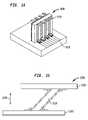
- FIG. 8is an elevational view illustrating a stacked microelectronic assembly according to an embodiment of the invention.
- FIG. 9is a sectional view of a stacked microelectronic assembly in accordance with one embodiment of the invention.
- FIG. 10is a corresponding perspective view of the stacked assembly shown in FIG. 9 .
- FIG. 11illustrates a variation of the embodiment described relative to FIGS. 9 and 10 , in which one or more inductive elements are integrated into interconnect panels of a stacked assembly.
- FIGS. 12-14are perspective views illustrating further embodiments in which interconnect panels are mounted to circuit panels.
- FIG. 15is an elevational view illustrating an assembly according to another embodiment of the invention in which an overlying circuit panel only partially overlies a lower circuit panel.
- Embodiments of the invention presented hereinrelate to a new way of interconnecting conductive elements disposed on circuit panels at different levels of a stacked assembly of circuit panels.
- a circuit panel having vertically rising conductive elementsprovides interconnection between horizontally disposed circuit panels at different levels of the stacked assembly.
- the terms “horizontal” and “vertical” used hereinare not meant to define absolutes, but rather to indicate relationships between elements.
- one circuit panelhas contacts exposed at a horizontal plane, and a “vertical” circuit panel means one that is oriented in a direction transverse to the horizontal plane.
- Another type of stacked packaging disclosed in U.S. patent application Ser. No. 10/746,810utilizes a ribbon-like flexible circuit panel on which an RF chip is mounted on a lower level, and the flexible circuit panel is then folded over, and another chip such as a digital or analog chip is mounted to the folded portion.
- Such arrangementmay require routing a relatively high number of signal lines to and from the digital chip to the top of the assembly through each bend of the flexible circuit panel to inputs and outputs at the lowest level of the package.
- Embodiments of the inventionprovide alternative ways of routing signal lines between levels in a stacked assembly.
- FIG. 1is a cutaway sectional view illustrating an embodiment of the invention.
- an assemblyincludes a first circuit panel 102 , on which a plurality of traces 104 are disposed.
- the first circuit panelis preferably of the type BT resin, although other preferred types of circuit panels include FR-4 or other epoxy glass resin, or glass.
- the first circuit panel 102preferably also includes a plurality of internal traces (not shown) . Some of the traces 104 and the internal traces are connected to terminals 106 . Some of the terminals 106 are connected by through holes (not shown) to a conductive plane 105 on a bottom surface of the assembly.
- the conductive plane 105preferably includes open areas or other openings in which bottom terminals (not shown) of the first circuit panel are disposed, at least some of the bottom terminals being connected to some of the terminals 106 disposed on the top surface of the first circuit panel.
- a plurality of other componentssuch as discrete components, active components or passive components are mounted to terminals of the first circuit panel.
- Passive componentssuch as passive chips have functions that are generally limited to providing a source of resistance, capacitance or inductance.
- active componentssuch as active chips have additional functions such as amplification, switching, filtering, rectification, regulation, etc., and are not limited to providing resistance, capacitance or inductance.
- an active chip 110is mounted to a top surface of the first circuit panel.
- the active chipis an RF power amplifier (RFPA) chip such as used in an RF transmitter device, or, alternatively, has an RF receiver function.
- RFPARF power amplifier
- Other active chips, passive chips and/or other components 120 , 122 , 124are preferably mounted to a top surface of the first circuit panel.
- a second circuit panel 130is disposed above at least a portion of the first circuit panel 102 , the second circuit panel having a construction like that described above for the first circuit panel, the second circuit panel also having components such as chips or other components (not shown) mounted thereon.
- a third circuit panel 150is further disposed above at least a portion of the second circuit panel 130 , the third circuit panel having a construction like that described above for the first circuit panel, the third circuit panel also having components such as chips or other components (not shown) mounted thereon.
- the second circuit panel 130is mounted to the first circuit panels 102 by first level interconnect panels 140 .
- the first level interconnect panels 140have a bottom surface (not shown) mounted to a top surface of the first circuit panel 102 , and the interconnect panels 140 further have a top surface mounted to a bottom surface of the second circuit panel 130 .
- the third circuit panel 150is mounted to the second circuit panel 130 by second level interconnect panels 142 .
- the second level interconnect panels 142have a bottom surface (not shown) mounted to a top surface of the second circuit panel 130 , and the interconnect panels 142 further have a top surface mounted to a bottom surface of the third circuit panel 150 .
- FIGS. 3A and 3Bare further perspective views of front and back surfaces of an interconnect panel 140 according to a preferred embodiment. While the placement of interconnect panels 140 , 142 is different, their structure is preferably the same. Accordingly, the following description applies to both.
- each interconnect panel 140includes a dielectric element 144 .
- the dielectric elementis of the type BT resin, in order for its coefficient of thermal expansion (CTE) to match that of the first, second and third circuit panels, which are also preferably of that type.
- the interconnect panels and circuit panelscan have dielectric elements made of other dielectric materials that have isotropic CTEs that are preferably the same or close to each other in value.
- a conductive plane 145is disposed on a rear surface 135 of the interconnect panel for providing a connection to ground, shielding or a source of power, for example. More preferably, the conductive plane 145 is a ground plane. Preferably, the conductive plane 145 is a continuous and relatively thick element, e.g., about 4 mils or more, for providing both electromagnetic shielding and conduction of heat.
- Each interconnect panel 140 , 142further includes a plurality of interconnect traces 146 on the dielectric element 144 , the interconnect traces formed of a conductive material such as a metal for allowing interconnections to be made to conductive traces 104 and/or terminals 106 of the first, second and third circuit panels.
- the interconnect tracespreferably have spacings of about 200 ⁇ m.
- the interconnect traces 146are disposed on a surface of the dielectric element 144 , such as a front surface 125 , so as to be separated from the conductive plane 145 by the thickness of the dielectric element 144 .
- the thickness of the dielectric element 144is comparable to or the same as that of the circuit panels, e.g., circuit panel 102 , and such thickness is preferably constant between the front and rear surfaces 125 , 135 .
- An arrangement of interconnect traces having a constant spacing relative to the conductive planeis an arrangement of parallel transmission lines. Such transmission line arrangement can be referred to as a microstrip.
- interconnect tracesare disposed internally within the dielectric element 144 . Whether the interconnect traces are disposed on the surface of the interconnect panel or internally, the traces are said to be disposed “on” the interconnect panel.
- the interconnect traces 146are connected to contacts 148 at the top end 152 and like or similar contacts (not shown) at the bottom end 154 of the interconnect panel, such contacts permitting mounting to conductive; elements of the first and second circuit panels.
- the contacts 148are provided as metalized grooves in the surface of dielectric element 144 at the top and bottom ends, the metalized grooves extending at least partially between the interconnect traces 146 on the front surface and the conductive plane 145 on the back surface.
- the height of the interconnect panel from the bottom end 154 to the top endis between about 200 ⁇ m and 1 mm for desirable RF signal performance.
- FIG. 3Bfurther illustrates a heat dissipating element 175 for mounting to the conductive plane 145 of the interconnect panel 140 , the element 175 having a plurality of outwardly extending metal fins 177 , for the purpose of increasing heat convection away from the conductive plane of the interconnect panel 140 .
- Such heat dissipating element 175may be a separate component or may be integrated with the interconnect panel 140 , and fabricated together therewith.
- the heat-dissipating elementmay include heat pipes for conducting heat away from a particular level of the stacked assembly 100 , such as a higher level (e.g., the second or third circuit panel levels). Referring again to FIG.
- the stacked assemblymay include additional heat conducting/dissipating elements such as a thermal conductor such as may take the form of a conductive heat slab 132 .
- a thermal conductorsuch as may take the form of a conductive heat slab 132 .
- Such slabpreferably is formed of copper or other good heat conductor, the slab being mounted, for example, to a rear surface of an active chip 110 (e.g., an RFPA), that is flip-chip mounted to the first circuit panel 102 .
- FIGS. 4A through 4DA variation of the above-described embodiment is illustrated in FIGS. 4A through 4D .
- the contacts 248 provided at the top end 152 and the bottom end 154 of the interconnect panel 240are planar or substantially planar elements rather than metalized grooves.
- the contacts 248extend as planar elements in a direction of a top plane defined by the top surface 249 of the interconnect panel 240 .
- the bottom contacts(not shown) extend as planar or substantially planar contacts in a direction of a bottom plane defined by the bottom surface of the interconnect panel.
- the interconnect traces 246extend substantially within a plane along the front surface 225 of the interconnect panel 240 .
- Planar or substantially planar conductive pads 250are conductively joined to the interconnect traces 246 at the top end 252 of the interconnect panel and planar or substantially planar conductive pads 251 are conductively joined to the interconnect traces 246 at the bottom end 254 of the interconnect panel 240 .
- the conductive padsare preferably wettable by a fusible conductive medium such as solder, tin or eutectic composition.
- a set of conductive pads 260 connected to conductive traces 262are exposed at a top surface 270 of a lower circuit panel 272 or circuit board to be joined to the conductive pads.
- conductive pads 251 on the front surface 240 of the interconnect panelare solidly bonded via the fusible conductive medium to the conductive pads 260 adjacent thereto on the top surface 270 of the lower circuit panel 270 .
- planar shape of the conductive padsmay help to promote greater adhesion with the fusible conductive medium, as compared to the concave metalized grooves present at the top and bottom ends of the above-described interconnect panel which might fail to be contacted over as great a surface area.
- the conductive padscan be formed in a manner appropriate to be joined by conductive paste.
- the conductive pastecan include any of many well-known conductive paste materials, among which are solder paste, silver-filled epoxy, and many others. In each such case, the paste is applied in a flowable or gel-like form, which hardens subsequently upon application of heat.
- FIG. 4Bis a top-down plan view illustrating a preferred spacing of two rows of conductive pads 260 exposed at the top surface 270 of the lower circuit panel.
- a first or “left-side” row 261 of padsis to be mounted to a row of corresponding pads exposed at a first edge of the front surface 225 with either the top end 152 or the bottom end 154 , or to a row of corresponding pads at one edge of the rear surface 235 with either the top end 152 or the bottom end 154 .
- a second or “right-side” row 263 of padsis to be mounted to a row of corresponding pads (not shown) exposed at an edge of the interconnect panel opposite the first edge.
- each pad 260preferably has a diameter 264 which is somewhat larger than the width of the conductive trace 262 to which it is connected. The distance between edges of each pad 260 is referred to as the “pad space” 266 .
- FIG. 4Cis a plan view of the interconnect panel 240 looking towards a bottom end 254 .
- the interconnect panelhas a thickness 265 , being essentially the thickness of the dielectric element thereof, and a pitch 267 , which is defined as the center-to-center distance between adjacent parallel conductive traces exposed at the bottom end 254 .
- FIG. 4Dis a partial top-down plan view illustrating a preferred arrangement for aligning and mounting the conductive pads of the interconnect panel 240 to conductive pads of the lower circuit panel 272 .
- the interconnect panel 240preferably overlaps edges 276 of the conductive pads 260 of the lower circuit panel 272 , by a distance 278 .
- the conductive pads(shown in dotted line form as underlying interconnect panel 240 ) are preferably only partially overlapped by the conductive pads 260 of the lower circuit panel.
- 265denotes the thickness of the interconnect panel.
- conductive pads 251are disposed on the front and rear surfaces of the interconnect panel.
- the structure in which conductive pads 251 are disposed on the front and rear surfaces of the interconnect panelis beneficial to the formation of solder fillets on the front and rear surfaces.
- each row of pads 261 , 263is disposed at a space 266 which is smaller than or no greater than the thickness of the interconnect panel, this helps to assure that conductive material, e.g., solder, conductive paste, disposed on the conductive pads of the lower circuit panel will flow onto the conductive pads 251 on the front or rear surface of the interconnect panel. This, in turn, helps the interconnect panel to be disposed at a right angle to the lower circuit panel.
- FIG. 4Eis a perspective view of a panel 340 designed to function as an antenna or inductive coil, rather than primarily as an interconnect element.
- the panelincludes conductive contacts at at least one edge.
- the contactsmay be in form of metalized grooves of conductive traces and pads.
- an antennais provided in form of a helical coiled element, formed by spiraled conductive traces formed on one or more dielectric layers of the panel 340 .
- Metalized through vias 342can provide interconnection between respective layers.
- metalized grooves or traces extending between the front surface 352 and the rear surface 354 at the top end or bottom endcan provide interconnection between respective layers.
- the panel 340can function as a stand-alone antenna element for mounting to a circuit panel in a manner similar to that described relative to FIG. 4D , for example.
- the panel 340can include interconnect traces as well as inductive, e.g., antenna elements, or can even provide interconnect traces combined with inductive elements.
- the panel 340can be used in stacked assemblies at locations where an interconnect panel or such as described above would be used, or can be mounted at other locations in stacked assemblies which already have such interconnect panels.
- the interconnect panelincludes conductive planes 170 disposed on the front and back surfaces of a dielectric element 164 , and the interconnect traces 162 are disposed internally within the dielectric element 164 , such that interconnect traces 162 are disposed in a strip-line arrangement in relation to the conductive planes 170 .
- Such strip-line arrangementpermits good transfer of signals along the internal interconnect traces 162 , especially for signals in higher radio frequency ranges.
- FIG. 2The particular mounting arrangement of the circuit panels and interconnect panels is further shown in the sectional view of FIG. 2 .
- the features referenced in FIGS. 1 and 3 A- 3 Bare also referenced in FIG. 2 to the extent that they appear therein.
- bottom ends of first level interconnect panels 140have contacts 148 mounted to terminals 106 on a top surface 112 of the first circuit panel 102 , as by masses of solder 155 .
- a similar techniqueis used to mount the interconnect panels 140 to the second circuit panel, and to mount second level interconnect panels 142 to the second and third circuit panels 130 , 150 .
- diffusion bonding, adhesive bonding, eutectic bonding, or any other suitable methodcan be used to bond the contacts 148 of the interconnect panels 140 , 142 to the first and second circuit panels.
- FIG. 2An alternative technique is illustrated for mounting the second level interconnect panels 142 to the third circuit panel 150 .
- conductive traces 146 on the front surface of interconnect panels 142are bonded by solder masses 126 to terminals 116 on the front surface 157 of the third circuit panel 150 .
- the first, second and third circuit panels 102 , 130 , 150preferably have metalized sidewalls 136 for conductively connecting their conductive (ground) planes 105 together.
- other conductive elementssuch as metalized through holes, metalized grooves, conductive adhesives or solder masses may be used to conductively connect the conductive planes 105 of the circuit panels and the interconnect panels.
- FIGS. 6A-6Care plan views further illustrating the front surface 125 , rear surface 135 , and top end 152 of the interconnect panel described above relative to FIGS. 3 and 4 .
- FIG. 6Aillustrates the interconnect traces 146 disposed on the dielectric element 144 on the front surface 125 .
- FIG. 6Billustrates the conductive plane 145 disposed on the rear surface 135 .
- FIG. 6Cillustrates contacts 148 disposed on the top end 152 . While not specifically shown, the bottom surface has a similar appearance.
- FIG. 6Dillustrates a top end of an alternative interconnect panel 172 having an arrangement similar to that shown in FIG. 5 , except that ground traces 174 extend across the top end of the dielectric element. 164 .
- FIG. 6Eillustrates a method of fabricating an interconnect panel 140 such as that shown in FIGS. 3-4 .
- a dielectric element 600sized for a typical circuit board application, such as a BT resin board, is fabricated to have conductive traces 602 extending along the front surface 610 .
- Metalized through holes 604extend from the front surface 610 to the rear surface (not shown).
- the dielectric elementis cut along lines 620 and 622 to provide the interconnect panel, wherein the conductive traces 602 become the interconnect traces of the interconnect panel, and the metalized through holes or metalized vias are cut to become the contacts of the interconnect panel, the contacts appearing as grooves in the top and bottom surfaces of the interconnect panel.
- FIG. 7is a plan view of a top surface of a circuit panel 200 having components 205 , e.g., one or more chips, discrete or integrated passive components mounted thereto, the circuit panel 200 to be interconnected to another circuit panel in a manner similar to that described above relative to FIGS. 1 and 2 .
- Circuit panel 200includes a plurality of terminals 206 , each being horizontally offset in two directions from each other terminal 206 . Such arrangement permits closely spaced linearly extending contacts 148 on the top or bottom ends 152 , 154 ( FIGS. 3-4 ) to be bonded to neighboring ones of the terminals 206 .
- FIG. 8illustrates a variation of the stacked assembly shown and described above with respect to FIGS. 1 and 2 . As shown in FIG. 8 , the first and second circuit panels 300 , 400 overhang beyond the interconnect panels 350 .
- FIGS. 9 and 10illustrate an alternative embodiment in which each circuit panel 910 is disposed in a shelf-like arrangement in a stacked assembly.
- FIG. 9is a sectional view
- FIG. 10is a perspective view.
- the circuit panel 910preferably includes a ground plane 935
- the circuit panel 910is conductively mounted to a motherboard 920 for power, ground and heat conduction.
- the conductive plane 935preferably includes open areas or other openings in which bottom terminals (not shown) of the circuit panel 910 are disposed, at least some of the bottom terminals being connected to some of the terminals 940 disposed on the top surface of the circuit panel 910 . In such way, signal transfer may also be provided to and from motherboard 920 .
- the interconnect panels 900have notches 902 disposed in front surfaces 905 thereof on which conductive traces are disposed.
- the interconnect panels 900have conductive planes 915 , preferably being ground planes, the conductive planes 915 preferably being mounted to ground and/or heat conductors disposed on the motherboard 920 .
- An advantage of this arrangement over that shown and described relative to FIGS. 1 and 2is the continuous conductive plane that extends vertically to connect each of the first, second and third circuit panels.
- the conductive plane 915is preferably mounted directly to the ground planes 935 of the bottom and top ones of the circuit panels 910 .
- a connection 904 to the conductive plane 915may be provided through the dielectric element 901 in the case of the middle circuit panel 911 .
- terminals 940 on a top surface of the circuit panel 910are preferably bonded to terminals 941 on a bottom end of the interconnect panel 900 .
- terminals 942 on an end surface of the circuit panel 910are connected to internal traces 944 of the interconnect panel 900 .
- FIG. 11illustrates a variation of the embodiment described relative to FIGS. 9 and 10 , in which one or more inductive elements 1110 , e.g., antennas, are integrated into interconnect panels 1100 of a stacked assembly.
- the inductive elementsmay include those such as described in commonly owned co-pending U.S. patent application Ser. Nos. 10/210,160 filed Aug. 1, 2002 and 10/452,333 filed Jun. 2, 2003, the disclosures of which are hereby incorporated herein by reference.
- conductive planes 1115are disposed internally within the interconnect panels 1100 , and are separated from the inductive elements 1110 by dielectric layers 1112 , so as to provide shielding relative to the inductive elements.
- FIGS. 12-14illustrate further arrangements for mounting interconnect panels to circuit panels, according to various embodiments of the invention.
- an interconnect panel 1200has a lower end 1202 sized to fit within an opening 1205 of a circuit panel 1210 .
- Conductive traces (not shown) on a front surface 1220 of the interconnect panelare conductively connected to terminals of the circuit panel 1210 , as by pressure fit, soldering, bonding, or conductive adhesive bonding, etc.
- a conductive and/or thermally conductive plane 1230 disposed on a rear surface of the interconnect panel 1200is conductively connected to a conductive and/or thermally conductive element 1212 of the circuit panel.
- FIG. 13further illustrates an embodiment in which an interconnect panel has traces 1310 thereon which are bonded directly to traces 1320 on the front surface of a circuit panel 1330 by solder masses 1340 disposed thereon.
- solder masses 1340disposed thereon.
- One possible way of performing such solderingis to provide ring-shaped solder masses spaced apart on a rod of glass, or other material which may be a temporary element, and to contact the interconnect panel 1300 and the circuit panel 1330 . simultaneously with such rings to melt the rings and bond the traces 1310 of the interconnect panel to the traces 1320 of the circuit panel 1330 .
- FIG. 14illustrates an alternative embodiment of an interconnect panel 1400 in which conductive traces are provided with extensions 1410 integrated thereto, the extensions provided for mounting to traces 1420 of the circuit panel.
- FIG. 15further illustrates an assembly 1500 in which an overlying circuit panel 1510 only partially overlies a lower circuit panel 1520 , and the two circuit panels are interconnected by way of an interconnect panel 1530 that is slanted relative to a vertical axis 1540 of the assembly.
Landscapes
- Engineering & Computer Science (AREA)
- Manufacturing & Machinery (AREA)
- Microelectronics & Electronic Packaging (AREA)
- Combinations Of Printed Boards (AREA)
Abstract
Description
Claims (26)
Priority Applications (1)
| Application Number | Priority Date | Filing Date | Title |
|---|---|---|---|
| US11/143,201US7489524B2 (en) | 2004-06-02 | 2005-06-02 | Assembly including vertical and horizontal joined circuit panels |
Applications Claiming Priority (2)
| Application Number | Priority Date | Filing Date | Title |
|---|---|---|---|
| US57617004P | 2004-06-02 | 2004-06-02 | |
| US11/143,201US7489524B2 (en) | 2004-06-02 | 2005-06-02 | Assembly including vertical and horizontal joined circuit panels |
Publications (2)
| Publication Number | Publication Date |
|---|---|
| US20050269693A1 US20050269693A1 (en) | 2005-12-08 |
| US7489524B2true US7489524B2 (en) | 2009-02-10 |
Family
ID=34982474
Family Applications (1)
| Application Number | Title | Priority Date | Filing Date |
|---|---|---|---|
| US11/143,201Expired - Fee RelatedUS7489524B2 (en) | 2004-06-02 | 2005-06-02 | Assembly including vertical and horizontal joined circuit panels |
Country Status (2)
| Country | Link |
|---|---|
| US (1) | US7489524B2 (en) |
| WO (1) | WO2005119765A2 (en) |
Cited By (32)
| Publication number | Priority date | Publication date | Assignee | Title |
|---|---|---|---|---|
| US20120043119A1 (en)* | 2009-06-02 | 2012-02-23 | Hsio Technologies, Llc | Composite polymer-metal electrical contacts |
| US20120235876A1 (en)* | 2009-11-27 | 2012-09-20 | Richard John Harper | Antenna array |
| US20150022986A1 (en)* | 2013-07-19 | 2015-01-22 | Motorola Mobility Llc | Circuit Assembly and Corresponding Methods |
| US9054097B2 (en) | 2009-06-02 | 2015-06-09 | Hsio Technologies, Llc | Compliant printed circuit area array semiconductor device package |
| US9076884B2 (en) | 2009-06-02 | 2015-07-07 | Hsio Technologies, Llc | Compliant printed circuit semiconductor package |
| US9093767B2 (en) | 2009-06-02 | 2015-07-28 | Hsio Technologies, Llc | High performance surface mount electrical interconnect |
| US9136196B2 (en) | 2009-06-02 | 2015-09-15 | Hsio Technologies, Llc | Compliant printed circuit wafer level semiconductor package |
| US9184527B2 (en) | 2009-06-02 | 2015-11-10 | Hsio Technologies, Llc | Electrical connector insulator housing |
| US9184145B2 (en) | 2009-06-02 | 2015-11-10 | Hsio Technologies, Llc | Semiconductor device package adapter |
| US9196980B2 (en) | 2009-06-02 | 2015-11-24 | Hsio Technologies, Llc | High performance surface mount electrical interconnect with external biased normal force loading |
| US9232654B2 (en) | 2009-06-02 | 2016-01-05 | Hsio Technologies, Llc | High performance electrical circuit structure |
| US9231328B2 (en) | 2009-06-02 | 2016-01-05 | Hsio Technologies, Llc | Resilient conductive electrical interconnect |
| US9276336B2 (en) | 2009-05-28 | 2016-03-01 | Hsio Technologies, Llc | Metalized pad to electrical contact interface |
| US9276339B2 (en) | 2009-06-02 | 2016-03-01 | Hsio Technologies, Llc | Electrical interconnect IC device socket |
| US9320144B2 (en) | 2009-06-17 | 2016-04-19 | Hsio Technologies, Llc | Method of forming a semiconductor socket |
| US9320133B2 (en) | 2009-06-02 | 2016-04-19 | Hsio Technologies, Llc | Electrical interconnect IC device socket |
| US9318862B2 (en) | 2009-06-02 | 2016-04-19 | Hsio Technologies, Llc | Method of making an electronic interconnect |
| US9350093B2 (en) | 2010-06-03 | 2016-05-24 | Hsio Technologies, Llc | Selective metalization of electrical connector or socket housing |
| US20160174377A1 (en)* | 2014-12-16 | 2016-06-16 | Motorola Solutions, Inc | Method and apparatus for intrinsically safe circuit board arrangement for portable electronic devices |
| US9414500B2 (en) | 2009-06-02 | 2016-08-09 | Hsio Technologies, Llc | Compliant printed flexible circuit |
| US9536815B2 (en) | 2009-05-28 | 2017-01-03 | Hsio Technologies, Llc | Semiconductor socket with direct selective metalization |
| US9559447B2 (en) | 2015-03-18 | 2017-01-31 | Hsio Technologies, Llc | Mechanical contact retention within an electrical connector |
| US9603249B2 (en) | 2009-06-02 | 2017-03-21 | Hsio Technologies, Llc | Direct metalization of electrical circuit structures |
| US9613841B2 (en) | 2009-06-02 | 2017-04-04 | Hsio Technologies, Llc | Area array semiconductor device package interconnect structure with optional package-to-package or flexible circuit to package connection |
| US9660368B2 (en) | 2009-05-28 | 2017-05-23 | Hsio Technologies, Llc | High performance surface mount electrical interconnect |
| US9689897B2 (en) | 2010-06-03 | 2017-06-27 | Hsio Technologies, Llc | Performance enhanced semiconductor socket |
| US9699906B2 (en) | 2009-06-02 | 2017-07-04 | Hsio Technologies, Llc | Hybrid printed circuit assembly with low density main core and embedded high density circuit regions |
| US9761520B2 (en) | 2012-07-10 | 2017-09-12 | Hsio Technologies, Llc | Method of making an electrical connector having electrodeposited terminals |
| US9930775B2 (en) | 2009-06-02 | 2018-03-27 | Hsio Technologies, Llc | Copper pillar full metal via electrical circuit structure |
| US10159154B2 (en) | 2010-06-03 | 2018-12-18 | Hsio Technologies, Llc | Fusion bonded liquid crystal polymer circuit structure |
| US10506722B2 (en) | 2013-07-11 | 2019-12-10 | Hsio Technologies, Llc | Fusion bonded liquid crystal polymer electrical circuit structure |
| US10667410B2 (en) | 2013-07-11 | 2020-05-26 | Hsio Technologies, Llc | Method of making a fusion bonded circuit structure |
Families Citing this family (11)
| Publication number | Priority date | Publication date | Assignee | Title |
|---|---|---|---|---|
| JP2015065553A (en)* | 2013-09-25 | 2015-04-09 | 株式会社東芝 | Connection member, semiconductor device, and laminate structure |
| US9468103B2 (en)* | 2014-10-08 | 2016-10-11 | Raytheon Company | Interconnect transition apparatus |
| US9660333B2 (en) | 2014-12-22 | 2017-05-23 | Raytheon Company | Radiator, solderless interconnect thereof and grounding element thereof |
| US9780458B2 (en) | 2015-10-13 | 2017-10-03 | Raytheon Company | Methods and apparatus for antenna having dual polarized radiating elements with enhanced heat dissipation |
| US20180062434A1 (en) | 2016-08-26 | 2018-03-01 | Nucurrent, Inc. | Wireless Connector Receiver Module Circuit |
| US10361485B2 (en) | 2017-08-04 | 2019-07-23 | Raytheon Company | Tripole current loop radiating element with integrated circularly polarized feed |
| CN113015324B (en)* | 2019-12-19 | 2023-05-09 | 华为技术有限公司 | Circuit board assembly, electronic device, method for processing circuit board assembly |
| CN113923920B (en)* | 2020-07-09 | 2023-05-09 | 比亚迪股份有限公司 | Filter module and electronic device with same |
| CN116326219B (en) | 2020-10-02 | 2024-03-26 | 塞林克公司 | Form connections with flexible interconnect circuits |
| US11876312B2 (en) | 2020-10-02 | 2024-01-16 | Cellink Corporation | Methods and systems for terminal-free circuit connectors and flexible multilayered interconnect circuits |
| CN113067191B (en)* | 2021-03-19 | 2022-03-01 | 成都雷电微晶科技有限公司 | Tile type module power supply switching structure |
Citations (18)
| Publication number | Priority date | Publication date | Assignee | Title |
|---|---|---|---|---|
| US3496634A (en)* | 1966-12-30 | 1970-02-24 | Ibm | Method of wiring and metal embedding an electrical back panel |
| US3614541A (en) | 1969-04-08 | 1971-10-19 | North American Rockwell | Package for an electronic assembly |
| US4502098A (en) | 1981-02-10 | 1985-02-26 | Brown David F | Circuit assembly |
| FR2575336A1 (en) | 1984-12-21 | 1986-06-27 | Francelco Sa | Connector having non-sliding contacts |
| FR2608328A1 (en) | 1986-12-10 | 1988-06-17 | Ducellier & Cie | Method for connecting a first printed circuit to a second printed circuit, and printed circuits which enable such a method to be implemented and which are interconnected in this way |
| US4868712A (en) | 1987-02-04 | 1989-09-19 | Woodman John K | Three dimensional integrated circuit package |
| DE4136355A1 (en) | 1991-11-05 | 1993-05-06 | Smt & Hybrid Gmbh, O-8010 Dresden, De | Three=dimensional assembly of electronic components and sensors, e.g. for accelerometer mfr. - interconnecting substrates with solder joints, conductive adhesive or wire bonds to edges of polyhedron |
| US5723901A (en) | 1994-12-13 | 1998-03-03 | Kabushiki Kaisha Toshiba | Stacked semiconductor device having peripheral through holes |
| JPH11121896A (en) | 1997-10-16 | 1999-04-30 | Toshiba Corp | Circuit wiring board and method of manufacturing the same |
| US6172874B1 (en) | 1998-04-06 | 2001-01-09 | Silicon Graphics, Inc. | System for stacking of integrated circuit packages |
| US6239386B1 (en)* | 1994-07-19 | 2001-05-29 | Tessera, Inc. | Electrical connections with deformable contacts |
| US6265765B1 (en)* | 1994-07-07 | 2001-07-24 | Tessera, Inc. | Fan-out semiconductor chip assembly |
| EP1191635A2 (en) | 2000-09-19 | 2002-03-27 | Nissan Motor Co., Ltd. | Interconnect structure |
| US20040032011A1 (en) | 2001-08-28 | 2004-02-19 | Tessera, Inc. | Microelectronic assemblies incorporating inductors |
| US20040238857A1 (en) | 2001-08-28 | 2004-12-02 | Tessera, Inc. | High frequency chip packages with connecting elements |
| WO2005019319A1 (en) | 2003-08-21 | 2005-03-03 | Innovene Europe Limited | Expandable polystyrene composition |
| US20060008945A1 (en)* | 2001-10-26 | 2006-01-12 | Staktek Group, L.P. | Integrated circuit stacking system and method |
| US7033861B1 (en)* | 2005-05-18 | 2006-04-25 | Staktek Group L.P. | Stacked module systems and method |
- 2005
- 2005-06-02WOPCT/US2005/019319patent/WO2005119765A2/enactiveApplication Filing
- 2005-06-02USUS11/143,201patent/US7489524B2/ennot_activeExpired - Fee Related
Patent Citations (19)
| Publication number | Priority date | Publication date | Assignee | Title |
|---|---|---|---|---|
| US3496634A (en)* | 1966-12-30 | 1970-02-24 | Ibm | Method of wiring and metal embedding an electrical back panel |
| US3614541A (en) | 1969-04-08 | 1971-10-19 | North American Rockwell | Package for an electronic assembly |
| US4502098A (en) | 1981-02-10 | 1985-02-26 | Brown David F | Circuit assembly |
| FR2575336A1 (en) | 1984-12-21 | 1986-06-27 | Francelco Sa | Connector having non-sliding contacts |
| FR2608328A1 (en) | 1986-12-10 | 1988-06-17 | Ducellier & Cie | Method for connecting a first printed circuit to a second printed circuit, and printed circuits which enable such a method to be implemented and which are interconnected in this way |
| US4868712A (en) | 1987-02-04 | 1989-09-19 | Woodman John K | Three dimensional integrated circuit package |
| DE4136355A1 (en) | 1991-11-05 | 1993-05-06 | Smt & Hybrid Gmbh, O-8010 Dresden, De | Three=dimensional assembly of electronic components and sensors, e.g. for accelerometer mfr. - interconnecting substrates with solder joints, conductive adhesive or wire bonds to edges of polyhedron |
| US6265765B1 (en)* | 1994-07-07 | 2001-07-24 | Tessera, Inc. | Fan-out semiconductor chip assembly |
| US6239386B1 (en)* | 1994-07-19 | 2001-05-29 | Tessera, Inc. | Electrical connections with deformable contacts |
| US5723901A (en) | 1994-12-13 | 1998-03-03 | Kabushiki Kaisha Toshiba | Stacked semiconductor device having peripheral through holes |
| JPH11121896A (en) | 1997-10-16 | 1999-04-30 | Toshiba Corp | Circuit wiring board and method of manufacturing the same |
| US6172874B1 (en) | 1998-04-06 | 2001-01-09 | Silicon Graphics, Inc. | System for stacking of integrated circuit packages |
| EP1191635A2 (en) | 2000-09-19 | 2002-03-27 | Nissan Motor Co., Ltd. | Interconnect structure |
| US20040032011A1 (en) | 2001-08-28 | 2004-02-19 | Tessera, Inc. | Microelectronic assemblies incorporating inductors |
| US20040238857A1 (en) | 2001-08-28 | 2004-12-02 | Tessera, Inc. | High frequency chip packages with connecting elements |
| US6856007B2 (en) | 2001-08-28 | 2005-02-15 | Tessera, Inc. | High-frequency chip packages |
| US20060008945A1 (en)* | 2001-10-26 | 2006-01-12 | Staktek Group, L.P. | Integrated circuit stacking system and method |
| WO2005019319A1 (en) | 2003-08-21 | 2005-03-03 | Innovene Europe Limited | Expandable polystyrene composition |
| US7033861B1 (en)* | 2005-05-18 | 2006-04-25 | Staktek Group L.P. | Stacked module systems and method |
Non-Patent Citations (3)
| Title |
|---|
| International Search Report, PCT/US2005/019319, Dated Dec. 1, 2005. |
| Jensen, Improved Method for Characterizing and Modeling Gigabit Flex-Circuit Based Interconnects, 2001 High-Performance System Design Conference, DesignCon 2001. |
| Rinne, The Parasitic Reactances of Flip Chip Solder Bumps, Unitive Electronics, Inc., Research Triangle Park, NC, North Carolina State University, Raleigh, NC. |
Cited By (40)
| Publication number | Priority date | Publication date | Assignee | Title |
|---|---|---|---|---|
| US9276336B2 (en) | 2009-05-28 | 2016-03-01 | Hsio Technologies, Llc | Metalized pad to electrical contact interface |
| US9660368B2 (en) | 2009-05-28 | 2017-05-23 | Hsio Technologies, Llc | High performance surface mount electrical interconnect |
| US9536815B2 (en) | 2009-05-28 | 2017-01-03 | Hsio Technologies, Llc | Semiconductor socket with direct selective metalization |
| US9699906B2 (en) | 2009-06-02 | 2017-07-04 | Hsio Technologies, Llc | Hybrid printed circuit assembly with low density main core and embedded high density circuit regions |
| US9277654B2 (en)* | 2009-06-02 | 2016-03-01 | Hsio Technologies, Llc | Composite polymer-metal electrical contacts |
| US9076884B2 (en) | 2009-06-02 | 2015-07-07 | Hsio Technologies, Llc | Compliant printed circuit semiconductor package |
| US9093767B2 (en) | 2009-06-02 | 2015-07-28 | Hsio Technologies, Llc | High performance surface mount electrical interconnect |
| US9136196B2 (en) | 2009-06-02 | 2015-09-15 | Hsio Technologies, Llc | Compliant printed circuit wafer level semiconductor package |
| US9414500B2 (en) | 2009-06-02 | 2016-08-09 | Hsio Technologies, Llc | Compliant printed flexible circuit |
| US9184145B2 (en) | 2009-06-02 | 2015-11-10 | Hsio Technologies, Llc | Semiconductor device package adapter |
| US9196980B2 (en) | 2009-06-02 | 2015-11-24 | Hsio Technologies, Llc | High performance surface mount electrical interconnect with external biased normal force loading |
| US9232654B2 (en) | 2009-06-02 | 2016-01-05 | Hsio Technologies, Llc | High performance electrical circuit structure |
| US9231328B2 (en) | 2009-06-02 | 2016-01-05 | Hsio Technologies, Llc | Resilient conductive electrical interconnect |
| US9930775B2 (en) | 2009-06-02 | 2018-03-27 | Hsio Technologies, Llc | Copper pillar full metal via electrical circuit structure |
| US9603249B2 (en) | 2009-06-02 | 2017-03-21 | Hsio Technologies, Llc | Direct metalization of electrical circuit structures |
| US9276339B2 (en) | 2009-06-02 | 2016-03-01 | Hsio Technologies, Llc | Electrical interconnect IC device socket |
| US9184527B2 (en) | 2009-06-02 | 2015-11-10 | Hsio Technologies, Llc | Electrical connector insulator housing |
| US9320133B2 (en) | 2009-06-02 | 2016-04-19 | Hsio Technologies, Llc | Electrical interconnect IC device socket |
| US9318862B2 (en) | 2009-06-02 | 2016-04-19 | Hsio Technologies, Llc | Method of making an electronic interconnect |
| US10609819B2 (en) | 2009-06-02 | 2020-03-31 | Hsio Technologies, Llc | Hybrid printed circuit assembly with low density main core and embedded high density circuit regions |
| US20120043119A1 (en)* | 2009-06-02 | 2012-02-23 | Hsio Technologies, Llc | Composite polymer-metal electrical contacts |
| US9054097B2 (en) | 2009-06-02 | 2015-06-09 | Hsio Technologies, Llc | Compliant printed circuit area array semiconductor device package |
| US9613841B2 (en) | 2009-06-02 | 2017-04-04 | Hsio Technologies, Llc | Area array semiconductor device package interconnect structure with optional package-to-package or flexible circuit to package connection |
| US9320144B2 (en) | 2009-06-17 | 2016-04-19 | Hsio Technologies, Llc | Method of forming a semiconductor socket |
| US20120235876A1 (en)* | 2009-11-27 | 2012-09-20 | Richard John Harper | Antenna array |
| US8941540B2 (en)* | 2009-11-27 | 2015-01-27 | Bae Systems Plc | Antenna array |
| US9689897B2 (en) | 2010-06-03 | 2017-06-27 | Hsio Technologies, Llc | Performance enhanced semiconductor socket |
| US9350093B2 (en) | 2010-06-03 | 2016-05-24 | Hsio Technologies, Llc | Selective metalization of electrical connector or socket housing |
| US10159154B2 (en) | 2010-06-03 | 2018-12-18 | Hsio Technologies, Llc | Fusion bonded liquid crystal polymer circuit structure |
| US9350124B2 (en) | 2010-12-01 | 2016-05-24 | Hsio Technologies, Llc | High speed circuit assembly with integral terminal and mating bias loading electrical connector assembly |
| US10453789B2 (en) | 2012-07-10 | 2019-10-22 | Hsio Technologies, Llc | Electrodeposited contact terminal for use as an electrical connector or semiconductor packaging substrate |
| US9761520B2 (en) | 2012-07-10 | 2017-09-12 | Hsio Technologies, Llc | Method of making an electrical connector having electrodeposited terminals |
| US10667410B2 (en) | 2013-07-11 | 2020-05-26 | Hsio Technologies, Llc | Method of making a fusion bonded circuit structure |
| US10506722B2 (en) | 2013-07-11 | 2019-12-10 | Hsio Technologies, Llc | Fusion bonded liquid crystal polymer electrical circuit structure |
| US20150022986A1 (en)* | 2013-07-19 | 2015-01-22 | Motorola Mobility Llc | Circuit Assembly and Corresponding Methods |
| US9363892B2 (en)* | 2013-07-19 | 2016-06-07 | Google Technology Holdings LLC | Circuit assembly and corresponding methods |
| US20160174377A1 (en)* | 2014-12-16 | 2016-06-16 | Motorola Solutions, Inc | Method and apparatus for intrinsically safe circuit board arrangement for portable electronic devices |
| US9980381B2 (en)* | 2014-12-16 | 2018-05-22 | Motorola Solutions, Inc. | Method and apparatus for intrinsically safe circuit board arrangement for portable electronic devices |
| US9755335B2 (en) | 2015-03-18 | 2017-09-05 | Hsio Technologies, Llc | Low profile electrical interconnect with fusion bonded contact retention and solder wick reduction |
| US9559447B2 (en) | 2015-03-18 | 2017-01-31 | Hsio Technologies, Llc | Mechanical contact retention within an electrical connector |
Also Published As
| Publication number | Publication date |
|---|---|
| WO2005119765A3 (en) | 2006-03-09 |
| WO2005119765A2 (en) | 2005-12-15 |
| US20050269693A1 (en) | 2005-12-08 |
Similar Documents
| Publication | Publication Date | Title |
|---|---|---|
| US7489524B2 (en) | Assembly including vertical and horizontal joined circuit panels | |
| US7087988B2 (en) | Semiconductor packaging apparatus | |
| US6037665A (en) | Mounting assembly of integrated circuit device and method for production thereof | |
| US9859250B2 (en) | Substrate and the method to fabricate thereof | |
| US7613010B2 (en) | Stereoscopic electronic circuit device, and relay board and relay frame used therein | |
| US7884458B2 (en) | Decoupling capacitor, wafer stack package including the decoupling capacitor, and method of fabricating the wafer stack package | |
| US8299594B2 (en) | Stacked ball grid array package module utilizing one or more interposer layers | |
| US20030198032A1 (en) | Integrated circuit assembly and method for making same | |
| US7754538B2 (en) | Packaging substrate structure with electronic components embedded therein and method for manufacturing the same | |
| WO2000014802A1 (en) | Semiconductor device, method of manufacture thereof, circuit board, and electronic device | |
| TW200307332A (en) | Low voltage drop and high thermal performance ball grid array package | |
| KR20040020945A (en) | Structure and method for fabrication of a leadless multi-die carrier | |
| JPH08340061A (en) | Ball grid array package | |
| KR20060101340A (en) | Stacked Semiconductor Device | |
| US9093442B1 (en) | Apparatus and method for achieving wideband RF performance and low junction to case thermal resistance in non-flip bump RFIC configuration | |
| CN106717135A (en) | Printed circuit board and printed circuit board arrangement | |
| KR20110128227A (en) | Multilayer printed board and its manufacturing method | |
| KR100618759B1 (en) | Hybrid module | |
| JP3081786B2 (en) | High frequency semiconductor device | |
| US6888227B2 (en) | Apparatus for routing signals | |
| JP2792494B2 (en) | Integrated circuit mounting structure | |
| JP2004153179A (en) | Semiconductor device and electronic device | |
| JPH10256428A (en) | Semiconductor package | |
| JP3879803B2 (en) | Semiconductor device and manufacturing method thereof, circuit board, and electronic apparatus | |
| US20250006585A1 (en) | Semiconductor packages with multiple types of conductive components |
Legal Events
| Date | Code | Title | Description |
|---|---|---|---|
| AS | Assignment | Owner name:TESSERA, INC., CALIFORNIA Free format text:ASSIGNMENT OF ASSIGNORS INTEREST;ASSIGNORS:GREEN, RONALD;KRISHNAN, SRIDHAR;WILSON, STUART E.;AND OTHERS;REEL/FRAME:016481/0341;SIGNING DATES FROM 20050608 TO 20050628 | |
| STCF | Information on status: patent grant | Free format text:PATENTED CASE | |
| CC | Certificate of correction | ||
| FPAY | Fee payment | Year of fee payment:4 | |
| FPAY | Fee payment | Year of fee payment:8 | |
| AS | Assignment | Owner name:ROYAL BANK OF CANADA, AS COLLATERAL AGENT, CANADA Free format text:SECURITY INTEREST;ASSIGNORS:INVENSAS CORPORATION;TESSERA, INC.;TESSERA ADVANCED TECHNOLOGIES, INC.;AND OTHERS;REEL/FRAME:040797/0001 Effective date:20161201 | |
| AS | Assignment | Owner name:BANK OF AMERICA, N.A., NORTH CAROLINA Free format text:SECURITY INTEREST;ASSIGNORS:ROVI SOLUTIONS CORPORATION;ROVI TECHNOLOGIES CORPORATION;ROVI GUIDES, INC.;AND OTHERS;REEL/FRAME:053468/0001 Effective date:20200601 | |
| AS | Assignment | Owner name:DTS, INC., CALIFORNIA Free format text:RELEASE BY SECURED PARTY;ASSIGNOR:ROYAL BANK OF CANADA;REEL/FRAME:052920/0001 Effective date:20200601 Owner name:TESSERA ADVANCED TECHNOLOGIES, INC, CALIFORNIA Free format text:RELEASE BY SECURED PARTY;ASSIGNOR:ROYAL BANK OF CANADA;REEL/FRAME:052920/0001 Effective date:20200601 Owner name:INVENSAS CORPORATION, CALIFORNIA Free format text:RELEASE BY SECURED PARTY;ASSIGNOR:ROYAL BANK OF CANADA;REEL/FRAME:052920/0001 Effective date:20200601 Owner name:TESSERA, INC., CALIFORNIA Free format text:RELEASE BY SECURED PARTY;ASSIGNOR:ROYAL BANK OF CANADA;REEL/FRAME:052920/0001 Effective date:20200601 Owner name:DTS LLC, CALIFORNIA Free format text:RELEASE BY SECURED PARTY;ASSIGNOR:ROYAL BANK OF CANADA;REEL/FRAME:052920/0001 Effective date:20200601 Owner name:IBIQUITY DIGITAL CORPORATION, MARYLAND Free format text:RELEASE BY SECURED PARTY;ASSIGNOR:ROYAL BANK OF CANADA;REEL/FRAME:052920/0001 Effective date:20200601 Owner name:INVENSAS BONDING TECHNOLOGIES, INC. (F/K/A ZIPTRONIX, INC.), CALIFORNIA Free format text:RELEASE BY SECURED PARTY;ASSIGNOR:ROYAL BANK OF CANADA;REEL/FRAME:052920/0001 Effective date:20200601 Owner name:FOTONATION CORPORATION (F/K/A DIGITALOPTICS CORPORATION AND F/K/A DIGITALOPTICS CORPORATION MEMS), CALIFORNIA Free format text:RELEASE BY SECURED PARTY;ASSIGNOR:ROYAL BANK OF CANADA;REEL/FRAME:052920/0001 Effective date:20200601 Owner name:PHORUS, INC., CALIFORNIA Free format text:RELEASE BY SECURED PARTY;ASSIGNOR:ROYAL BANK OF CANADA;REEL/FRAME:052920/0001 Effective date:20200601 | |
| FEPP | Fee payment procedure | Free format text:MAINTENANCE FEE REMINDER MAILED (ORIGINAL EVENT CODE: REM.); ENTITY STATUS OF PATENT OWNER: LARGE ENTITY | |
| LAPS | Lapse for failure to pay maintenance fees | Free format text:PATENT EXPIRED FOR FAILURE TO PAY MAINTENANCE FEES (ORIGINAL EVENT CODE: EXP.); ENTITY STATUS OF PATENT OWNER: LARGE ENTITY | |
| STCH | Information on status: patent discontinuation | Free format text:PATENT EXPIRED DUE TO NONPAYMENT OF MAINTENANCE FEES UNDER 37 CFR 1.362 | |
| FP | Lapsed due to failure to pay maintenance fee | Effective date:20210210 |