US7488658B2 - Stressed semiconductor device structures having granular semiconductor material - Google Patents
Stressed semiconductor device structures having granular semiconductor materialDownload PDFInfo
- Publication number
- US7488658B2 US7488658B2US11/531,372US53137206AUS7488658B2US 7488658 B2US7488658 B2US 7488658B2US 53137206 AUS53137206 AUS 53137206AUS 7488658 B2US7488658 B2US 7488658B2
- Authority
- US
- United States
- Prior art keywords
- nfet
- pfet
- spacers
- gate
- substrate
- Prior art date
- Legal status (The legal status is an assumption and is not a legal conclusion. Google has not performed a legal analysis and makes no representation as to the accuracy of the status listed.)
- Expired - Fee Related, expires
Links
- 239000004065semiconductorSubstances0.000titleclaimsabstractdescription20
- 239000000463materialSubstances0.000titleabstractdescription12
- 239000000758substrateSubstances0.000claimsabstractdescription15
- 238000000034methodMethods0.000claimsdescription55
- 229910021420polycrystalline siliconInorganic materials0.000claimsdescription29
- 229920005591polysiliconPolymers0.000claimsdescription10
- 125000006850spacer groupChemical group0.000claimsdescription9
- 238000000151depositionMethods0.000claimsdescription6
- 238000010438heat treatmentMethods0.000claims3
- 238000000137annealingMethods0.000abstractdescription7
- 238000004519manufacturing processMethods0.000abstractdescription7
- 238000002955isolationMethods0.000description8
- 238000005516engineering processMethods0.000description6
- 239000007772electrode materialSubstances0.000description5
- 239000007943implantSubstances0.000description5
- VYPSYNLAJGMNEJ-UHFFFAOYSA-NSilicium dioxideChemical groupO=[Si]=OVYPSYNLAJGMNEJ-UHFFFAOYSA-N0.000description4
- 238000001289rapid thermal chemical vapour depositionMethods0.000description4
- 238000004088simulationMethods0.000description4
- 238000013459approachMethods0.000description3
- 238000004140cleaningMethods0.000description3
- 238000001312dry etchingMethods0.000description3
- 125000001475halogen functional groupChemical group0.000description3
- 238000004518low pressure chemical vapour depositionMethods0.000description3
- 230000003647oxidationEffects0.000description3
- 238000007254oxidation reactionMethods0.000description3
- 229910021332silicideInorganic materials0.000description3
- FVBUAEGBCNSCDD-UHFFFAOYSA-Nsilicide(4-)Chemical compound[Si-4]FVBUAEGBCNSCDD-UHFFFAOYSA-N0.000description3
- 229910000577Silicon-germaniumInorganic materials0.000description2
- 230000015572biosynthetic processEffects0.000description2
- 229910052681coesiteInorganic materials0.000description2
- 229910052906cristobaliteInorganic materials0.000description2
- 230000008021depositionEffects0.000description2
- 238000010586diagramMethods0.000description2
- 238000005530etchingMethods0.000description2
- 229910052751metalInorganic materials0.000description2
- 239000002184metalSubstances0.000description2
- 238000000206photolithographyMethods0.000description2
- 229920002120photoresistant polymerPolymers0.000description2
- 238000012545processingMethods0.000description2
- 239000000377silicon dioxideSubstances0.000description2
- 229910052682stishoviteInorganic materials0.000description2
- 229910052905tridymiteInorganic materials0.000description2
- 229910052581Si3N4Inorganic materials0.000description1
- XUIMIQQOPSSXEZ-UHFFFAOYSA-NSiliconChemical compound[Si]XUIMIQQOPSSXEZ-UHFFFAOYSA-N0.000description1
- 229910052785arsenicInorganic materials0.000description1
- 230000006835compressionEffects0.000description1
- 238000007906compressionMethods0.000description1
- 238000005137deposition processMethods0.000description1
- 238000011982device technologyMethods0.000description1
- 239000003989dielectric materialSubstances0.000description1
- 238000009792diffusion processMethods0.000description1
- 229910000449hafnium oxideInorganic materials0.000description1
- WIHZLLGSGQNAGK-UHFFFAOYSA-Nhafnium(4+);oxygen(2-)Chemical compound[O-2].[O-2].[Hf+4]WIHZLLGSGQNAGK-UHFFFAOYSA-N0.000description1
- 238000002513implantationMethods0.000description1
- 238000001459lithographyMethods0.000description1
- 238000012986modificationMethods0.000description1
- 230000004048modificationEffects0.000description1
- 150000004767nitridesChemical class0.000description1
- TWNQGVIAIRXVLR-UHFFFAOYSA-Noxo(oxoalumanyloxy)alumaneChemical compoundO=[Al]O[Al]=OTWNQGVIAIRXVLR-UHFFFAOYSA-N0.000description1
- 238000000623plasma-assisted chemical vapour depositionMethods0.000description1
- 238000005498polishingMethods0.000description1
- 238000010405reoxidation reactionMethods0.000description1
- 230000035945sensitivityEffects0.000description1
- 229910052710siliconInorganic materials0.000description1
- 239000010703siliconSubstances0.000description1
- HQVNEWCFYHHQES-UHFFFAOYSA-Nsilicon nitrideChemical compoundN12[Si]34N5[Si]62N3[Si]51N64HQVNEWCFYHHQES-UHFFFAOYSA-N0.000description1
- 239000000126substanceSubstances0.000description1
- 238000012546transferMethods0.000description1
Images


Classifications
- H—ELECTRICITY
- H10—SEMICONDUCTOR DEVICES; ELECTRIC SOLID-STATE DEVICES NOT OTHERWISE PROVIDED FOR
- H10F—INORGANIC SEMICONDUCTOR DEVICES SENSITIVE TO INFRARED RADIATION, LIGHT, ELECTROMAGNETIC RADIATION OF SHORTER WAVELENGTH OR CORPUSCULAR RADIATION
- H10F30/00—Individual radiation-sensitive semiconductor devices in which radiation controls the flow of current through the devices, e.g. photodetectors
- H10F30/20—Individual radiation-sensitive semiconductor devices in which radiation controls the flow of current through the devices, e.g. photodetectors the devices having potential barriers, e.g. phototransistors
- H10F30/29—Individual radiation-sensitive semiconductor devices in which radiation controls the flow of current through the devices, e.g. photodetectors the devices having potential barriers, e.g. phototransistors the devices being sensitive to radiation having very short wavelengths, e.g. X-rays, gamma-rays or corpuscular radiation
- H10F30/298—Individual radiation-sensitive semiconductor devices in which radiation controls the flow of current through the devices, e.g. photodetectors the devices having potential barriers, e.g. phototransistors the devices being sensitive to radiation having very short wavelengths, e.g. X-rays, gamma-rays or corpuscular radiation the devices being characterised by field-effect operation, e.g. MIS type detectors
- H—ELECTRICITY
- H10—SEMICONDUCTOR DEVICES; ELECTRIC SOLID-STATE DEVICES NOT OTHERWISE PROVIDED FOR
- H10D—INORGANIC ELECTRIC SEMICONDUCTOR DEVICES
- H10D30/00—Field-effect transistors [FET]
- H10D30/60—Insulated-gate field-effect transistors [IGFET]
- H10D30/791—Arrangements for exerting mechanical stress on the crystal lattice of the channel regions
- H10D30/794—Arrangements for exerting mechanical stress on the crystal lattice of the channel regions comprising conductive materials, e.g. silicided source, drain or gate electrodes
- H—ELECTRICITY
- H01—ELECTRIC ELEMENTS
- H01L—SEMICONDUCTOR DEVICES NOT COVERED BY CLASS H10
- H01L21/00—Processes or apparatus adapted for the manufacture or treatment of semiconductor or solid state devices or of parts thereof
- H01L21/02—Manufacture or treatment of semiconductor devices or of parts thereof
- H01L21/04—Manufacture or treatment of semiconductor devices or of parts thereof the devices having potential barriers, e.g. a PN junction, depletion layer or carrier concentration layer
- H01L21/18—Manufacture or treatment of semiconductor devices or of parts thereof the devices having potential barriers, e.g. a PN junction, depletion layer or carrier concentration layer the devices having semiconductor bodies comprising elements of Group IV of the Periodic Table or AIIIBV compounds with or without impurities, e.g. doping materials
- H01L21/28—Manufacture of electrodes on semiconductor bodies using processes or apparatus not provided for in groups H01L21/20 - H01L21/268
- H01L21/28008—Making conductor-insulator-semiconductor electrodes
- H01L21/28017—Making conductor-insulator-semiconductor electrodes the insulator being formed after the semiconductor body, the semiconductor being silicon
- H01L21/28026—Making conductor-insulator-semiconductor electrodes the insulator being formed after the semiconductor body, the semiconductor being silicon characterised by the conductor
- H01L21/28035—Making conductor-insulator-semiconductor electrodes the insulator being formed after the semiconductor body, the semiconductor being silicon characterised by the conductor the final conductor layer next to the insulator being silicon, e.g. polysilicon, with or without impurities
- H—ELECTRICITY
- H01—ELECTRIC ELEMENTS
- H01L—SEMICONDUCTOR DEVICES NOT COVERED BY CLASS H10
- H01L21/00—Processes or apparatus adapted for the manufacture or treatment of semiconductor or solid state devices or of parts thereof
- H01L21/02—Manufacture or treatment of semiconductor devices or of parts thereof
- H01L21/04—Manufacture or treatment of semiconductor devices or of parts thereof the devices having potential barriers, e.g. a PN junction, depletion layer or carrier concentration layer
- H01L21/18—Manufacture or treatment of semiconductor devices or of parts thereof the devices having potential barriers, e.g. a PN junction, depletion layer or carrier concentration layer the devices having semiconductor bodies comprising elements of Group IV of the Periodic Table or AIIIBV compounds with or without impurities, e.g. doping materials
- H01L21/28—Manufacture of electrodes on semiconductor bodies using processes or apparatus not provided for in groups H01L21/20 - H01L21/268
- H01L21/28008—Making conductor-insulator-semiconductor electrodes
- H01L21/28017—Making conductor-insulator-semiconductor electrodes the insulator being formed after the semiconductor body, the semiconductor being silicon
- H01L21/28247—Making conductor-insulator-semiconductor electrodes the insulator being formed after the semiconductor body, the semiconductor being silicon passivation or protection of the electrode, e.g. using re-oxidation
- H—ELECTRICITY
- H01—ELECTRIC ELEMENTS
- H01L—SEMICONDUCTOR DEVICES NOT COVERED BY CLASS H10
- H01L21/00—Processes or apparatus adapted for the manufacture or treatment of semiconductor or solid state devices or of parts thereof
- H01L21/02—Manufacture or treatment of semiconductor devices or of parts thereof
- H01L21/04—Manufacture or treatment of semiconductor devices or of parts thereof the devices having potential barriers, e.g. a PN junction, depletion layer or carrier concentration layer
- H01L21/18—Manufacture or treatment of semiconductor devices or of parts thereof the devices having potential barriers, e.g. a PN junction, depletion layer or carrier concentration layer the devices having semiconductor bodies comprising elements of Group IV of the Periodic Table or AIIIBV compounds with or without impurities, e.g. doping materials
- H01L21/30—Treatment of semiconductor bodies using processes or apparatus not provided for in groups H01L21/20 - H01L21/26
- H01L21/324—Thermal treatment for modifying the properties of semiconductor bodies, e.g. annealing, sintering
- H—ELECTRICITY
- H01—ELECTRIC ELEMENTS
- H01L—SEMICONDUCTOR DEVICES NOT COVERED BY CLASS H10
- H01L21/00—Processes or apparatus adapted for the manufacture or treatment of semiconductor or solid state devices or of parts thereof
- H01L21/70—Manufacture or treatment of devices consisting of a plurality of solid state components formed in or on a common substrate or of parts thereof; Manufacture of integrated circuit devices or of parts thereof
- H01L21/71—Manufacture of specific parts of devices defined in group H01L21/70
- H01L21/76—Making of isolation regions between components
- H—ELECTRICITY
- H10—SEMICONDUCTOR DEVICES; ELECTRIC SOLID-STATE DEVICES NOT OTHERWISE PROVIDED FOR
- H10D—INORGANIC ELECTRIC SEMICONDUCTOR DEVICES
- H10D30/00—Field-effect transistors [FET]
- H10D30/01—Manufacture or treatment
- H10D30/021—Manufacture or treatment of FETs having insulated gates [IGFET]
- H10D30/0223—Manufacture or treatment of FETs having insulated gates [IGFET] having source and drain regions or source and drain extensions self-aligned to sides of the gate
- H10D30/0227—Manufacture or treatment of FETs having insulated gates [IGFET] having source and drain regions or source and drain extensions self-aligned to sides of the gate having both lightly-doped source and drain extensions and source and drain regions self-aligned to the sides of the gate, e.g. lightly-doped drain [LDD] MOSFET or double-diffused drain [DDD] MOSFET
- H—ELECTRICITY
- H10—SEMICONDUCTOR DEVICES; ELECTRIC SOLID-STATE DEVICES NOT OTHERWISE PROVIDED FOR
- H10D—INORGANIC ELECTRIC SEMICONDUCTOR DEVICES
- H10D64/00—Electrodes of devices having potential barriers
- H10D64/01—Manufacture or treatment
- H10D64/017—Manufacture or treatment using dummy gates in processes wherein at least parts of the final gates are self-aligned to the dummy gates, i.e. replacement gate processes
- H—ELECTRICITY
- H10—SEMICONDUCTOR DEVICES; ELECTRIC SOLID-STATE DEVICES NOT OTHERWISE PROVIDED FOR
- H10D—INORGANIC ELECTRIC SEMICONDUCTOR DEVICES
- H10D64/00—Electrodes of devices having potential barriers
- H10D64/60—Electrodes characterised by their materials
- H10D64/66—Electrodes having a conductor capacitively coupled to a semiconductor by an insulator, e.g. MIS electrodes
- H10D64/661—Electrodes having a conductor capacitively coupled to a semiconductor by an insulator, e.g. MIS electrodes the conductor comprising a layer of silicon contacting the insulator, e.g. polysilicon having vertical doping variation
- H10D64/662—Electrodes having a conductor capacitively coupled to a semiconductor by an insulator, e.g. MIS electrodes the conductor comprising a layer of silicon contacting the insulator, e.g. polysilicon having vertical doping variation the conductor further comprising additional layers, e.g. multiple silicon layers having different crystal structures
- H—ELECTRICITY
- H10—SEMICONDUCTOR DEVICES; ELECTRIC SOLID-STATE DEVICES NOT OTHERWISE PROVIDED FOR
- H10D—INORGANIC ELECTRIC SEMICONDUCTOR DEVICES
- H10D84/00—Integrated devices formed in or on semiconductor substrates that comprise only semiconducting layers, e.g. on Si wafers or on GaAs-on-Si wafers
- H10D84/01—Manufacture or treatment
- H10D84/0123—Integrating together multiple components covered by H10D12/00 or H10D30/00, e.g. integrating multiple IGBTs
- H10D84/0126—Integrating together multiple components covered by H10D12/00 or H10D30/00, e.g. integrating multiple IGBTs the components including insulated gates, e.g. IGFETs
- H10D84/0165—Integrating together multiple components covered by H10D12/00 or H10D30/00, e.g. integrating multiple IGBTs the components including insulated gates, e.g. IGFETs the components including complementary IGFETs, e.g. CMOS devices
- H10D84/0167—Manufacturing their channels
- H—ELECTRICITY
- H10—SEMICONDUCTOR DEVICES; ELECTRIC SOLID-STATE DEVICES NOT OTHERWISE PROVIDED FOR
- H10D—INORGANIC ELECTRIC SEMICONDUCTOR DEVICES
- H10D84/00—Integrated devices formed in or on semiconductor substrates that comprise only semiconducting layers, e.g. on Si wafers or on GaAs-on-Si wafers
- H10D84/01—Manufacture or treatment
- H10D84/0123—Integrating together multiple components covered by H10D12/00 or H10D30/00, e.g. integrating multiple IGBTs
- H10D84/0126—Integrating together multiple components covered by H10D12/00 or H10D30/00, e.g. integrating multiple IGBTs the components including insulated gates, e.g. IGFETs
- H10D84/0165—Integrating together multiple components covered by H10D12/00 or H10D30/00, e.g. integrating multiple IGBTs the components including insulated gates, e.g. IGFETs the components including complementary IGFETs, e.g. CMOS devices
- H10D84/0172—Manufacturing their gate conductors
- H10D84/0177—Manufacturing their gate conductors the gate conductors having different materials or different implants
- H—ELECTRICITY
- H10—SEMICONDUCTOR DEVICES; ELECTRIC SOLID-STATE DEVICES NOT OTHERWISE PROVIDED FOR
- H10D—INORGANIC ELECTRIC SEMICONDUCTOR DEVICES
- H10D84/00—Integrated devices formed in or on semiconductor substrates that comprise only semiconducting layers, e.g. on Si wafers or on GaAs-on-Si wafers
- H10D84/01—Manufacture or treatment
- H10D84/02—Manufacture or treatment characterised by using material-based technologies
- H10D84/03—Manufacture or treatment characterised by using material-based technologies using Group IV technology, e.g. silicon technology or silicon-carbide [SiC] technology
- H10D84/038—Manufacture or treatment characterised by using material-based technologies using Group IV technology, e.g. silicon technology or silicon-carbide [SiC] technology using silicon technology, e.g. SiGe
- H—ELECTRICITY
- H01—ELECTRIC ELEMENTS
- H01L—SEMICONDUCTOR DEVICES NOT COVERED BY CLASS H10
- H01L21/00—Processes or apparatus adapted for the manufacture or treatment of semiconductor or solid state devices or of parts thereof
- H01L21/02—Manufacture or treatment of semiconductor devices or of parts thereof
- H01L21/04—Manufacture or treatment of semiconductor devices or of parts thereof the devices having potential barriers, e.g. a PN junction, depletion layer or carrier concentration layer
- H01L21/18—Manufacture or treatment of semiconductor devices or of parts thereof the devices having potential barriers, e.g. a PN junction, depletion layer or carrier concentration layer the devices having semiconductor bodies comprising elements of Group IV of the Periodic Table or AIIIBV compounds with or without impurities, e.g. doping materials
- H01L21/26—Bombardment with radiation
- H01L21/263—Bombardment with radiation with high-energy radiation
- H01L21/265—Bombardment with radiation with high-energy radiation producing ion implantation
- H01L21/26506—Bombardment with radiation with high-energy radiation producing ion implantation in group IV semiconductors
- H01L21/26513—Bombardment with radiation with high-energy radiation producing ion implantation in group IV semiconductors of electrically active species
- H—ELECTRICITY
- H01—ELECTRIC ELEMENTS
- H01L—SEMICONDUCTOR DEVICES NOT COVERED BY CLASS H10
- H01L21/00—Processes or apparatus adapted for the manufacture or treatment of semiconductor or solid state devices or of parts thereof
- H01L21/02—Manufacture or treatment of semiconductor devices or of parts thereof
- H01L21/04—Manufacture or treatment of semiconductor devices or of parts thereof the devices having potential barriers, e.g. a PN junction, depletion layer or carrier concentration layer
- H01L21/18—Manufacture or treatment of semiconductor devices or of parts thereof the devices having potential barriers, e.g. a PN junction, depletion layer or carrier concentration layer the devices having semiconductor bodies comprising elements of Group IV of the Periodic Table or AIIIBV compounds with or without impurities, e.g. doping materials
- H01L21/26—Bombardment with radiation
- H01L21/263—Bombardment with radiation with high-energy radiation
- H01L21/265—Bombardment with radiation with high-energy radiation producing ion implantation
- H01L21/2658—Bombardment with radiation with high-energy radiation producing ion implantation of a molecular ion, e.g. decaborane
- H—ELECTRICITY
- H01—ELECTRIC ELEMENTS
- H01L—SEMICONDUCTOR DEVICES NOT COVERED BY CLASS H10
- H01L21/00—Processes or apparatus adapted for the manufacture or treatment of semiconductor or solid state devices or of parts thereof
- H01L21/02—Manufacture or treatment of semiconductor devices or of parts thereof
- H01L21/04—Manufacture or treatment of semiconductor devices or of parts thereof the devices having potential barriers, e.g. a PN junction, depletion layer or carrier concentration layer
- H01L21/18—Manufacture or treatment of semiconductor devices or of parts thereof the devices having potential barriers, e.g. a PN junction, depletion layer or carrier concentration layer the devices having semiconductor bodies comprising elements of Group IV of the Periodic Table or AIIIBV compounds with or without impurities, e.g. doping materials
- H01L21/28—Manufacture of electrodes on semiconductor bodies using processes or apparatus not provided for in groups H01L21/20 - H01L21/268
- H01L21/28008—Making conductor-insulator-semiconductor electrodes
- H01L21/28017—Making conductor-insulator-semiconductor electrodes the insulator being formed after the semiconductor body, the semiconductor being silicon
- H01L21/28158—Making the insulator
- H01L21/28167—Making the insulator on single crystalline silicon, e.g. using a liquid, i.e. chemical oxidation
- H—ELECTRICITY
- H10—SEMICONDUCTOR DEVICES; ELECTRIC SOLID-STATE DEVICES NOT OTHERWISE PROVIDED FOR
- H10D—INORGANIC ELECTRIC SEMICONDUCTOR DEVICES
- H10D30/00—Field-effect transistors [FET]
- H10D30/01—Manufacture or treatment
- H10D30/021—Manufacture or treatment of FETs having insulated gates [IGFET]
- H10D30/0212—Manufacture or treatment of FETs having insulated gates [IGFET] using self-aligned silicidation
- H—ELECTRICITY
- H10—SEMICONDUCTOR DEVICES; ELECTRIC SOLID-STATE DEVICES NOT OTHERWISE PROVIDED FOR
- H10D—INORGANIC ELECTRIC SEMICONDUCTOR DEVICES
- H10D62/00—Semiconductor bodies, or regions thereof, of devices having potential barriers
- H10D62/10—Shapes, relative sizes or dispositions of the regions of the semiconductor bodies; Shapes of the semiconductor bodies
- H10D62/17—Semiconductor regions connected to electrodes not carrying current to be rectified, amplified or switched, e.g. channel regions
- H10D62/351—Substrate regions of field-effect devices
- H10D62/357—Substrate regions of field-effect devices of FETs
- H10D62/364—Substrate regions of field-effect devices of FETs of IGFETs
- H10D62/371—Inactive supplementary semiconductor regions, e.g. for preventing punch-through, improving capacity effect or leakage current
- H—ELECTRICITY
- H10—SEMICONDUCTOR DEVICES; ELECTRIC SOLID-STATE DEVICES NOT OTHERWISE PROVIDED FOR
- H10D—INORGANIC ELECTRIC SEMICONDUCTOR DEVICES
- H10D64/00—Electrodes of devices having potential barriers
- H10D64/60—Electrodes characterised by their materials
- H10D64/66—Electrodes having a conductor capacitively coupled to a semiconductor by an insulator, e.g. MIS electrodes
- H10D64/68—Electrodes having a conductor capacitively coupled to a semiconductor by an insulator, e.g. MIS electrodes characterised by the insulator, e.g. by the gate insulator
- H10D64/691—Electrodes having a conductor capacitively coupled to a semiconductor by an insulator, e.g. MIS electrodes characterised by the insulator, e.g. by the gate insulator comprising metallic compounds, e.g. metal oxides or metal silicates
Definitions
- the present inventionrelates to semiconductor device structures, such as a CMOS device structure including both nFET and pFET devices.
- Mobility enhancementsare important to future semiconductor, e.g. CMOS device technologies. Performance improvements from conventional process technologies are becoming extremely difficult to achieve.
- Methods to stress Si channelsinclude: using SiGe which imparts stress from the bottom of the channel; different shallow trench isolation (STI) material choices which impart stresses from various sides, and SiN etch stop layers which also impart longitudinal stress from the sides.
- Drawbacks from the SiGe buffer layer or implanted-anneal-buffer approach with a strained Si cap layerare well known.
- Drawbacksinclude dislocations that impact yield severely, along with significant difficulty controlling As diffusion enhancements.
- the processis quite complicated and costly.
- the STI approachis less costly but is not self-aligned to the gate and has RX size sensitivity.
- the less costly approach of using nitride etch stop layers to create stressdoes produce some benefit, but the benefit is believed to be relatively marginal.
- the present inventionimproves device performance using channel mobility enhancement.
- the present inventionimproves mobility from the top of the channel by using the stress properties of properly modulated polysilicon gate stacks. Prior to the prevent invention these stress properties were very difficult to control.
- the present inventionincludes a method and structure which use small grain polysilicon to control stress properties.
- the present inventionprovides a method and a structure to impart compressive stress to the pFET channel and a tensile stress to the nFET channel.
- Other embodimentsinclude imparting compressive stress to the pFET channel while preventing compressive stress from being imparted to the nFET channel.
- Another embodiment of this inventionincludes imparting tensile stress to the nFET channel while preventing the tensile stress from being imparted to the pFET channel.
- the method of the present inventiondisposes (e.g., deposits) small grain poly-Si films in gate electrode stacks, which films become highly tensile as a result of annealing.
- the tensile film stresscan be suppressed by annealing with a low temperature deposited SiN film disposed on top of the poly-Si film.
- a method of fabricating a semiconductor device structureincludes providing a substrate; providing an electrode on the substrate; forming a recess in the electrode, the recess having an opening; disposing a small grain semiconductor material within the recess; covering the opening to contain the small grain semiconductor material within the recess, and then annealing the resultant structure.
- the present inventionalso includes a semiconductor device structure.
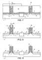
- FIGS. 1-9are side schematic views of process steps according to a preferred embodiment of the present invention.
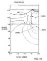
- FIG. 10is a diagram showing simulated stress contours in the gate and channel of the preferred inventive structure.
- the semiconductor substrateis a bulk Si substrate, an SOI substrate, or a stressed (strained) Si substrate.
- the substrateis a hybrid substrate which includes more than one surface orientation.
- the substratealternatively includes a semiconductor material other than Si, such as Ge or any combination of Group III-V elements or Group II-V elements.
- an isolation schemeis carried out. As is well known in semiconductor manufacturing, the isolation scheme is used to separate selected devices electrically from each other.
- the isolation schememay be a standard or a modified shallow trench isolation (STI) scheme.
- the STI 2is shown in FIG. 1 .
- the isolationis accomplished using a LOCOS process or mesa isolation scheme, as is well known in the art of fabricating semiconductor devices.
- the gate oxide 3is formed, for example, using a conventional thermal oxidation process.
- the oxide 3is formed using N 2 O, NO, O 2 or any combination of them.
- the oxidemay be nitridized using a conventional plasma process.
- the gate oxidemay be formed using a base oxide followed by deposition of a high k gate dielectric such as aluminum oxide, or hafnium oxide, or another high k gate dielectric.
- the gate dielectric material 3has an approximately ( ⁇ 10%) uniform thickness in the range of about ( ⁇ 10%) 0.6 nm to about 7 nm.
- a film 4is deposited over the entire wafer structure 1 , 2 , 3 .
- the film 4is used as a disposable (removable) or semi-disposable gate electrode material.
- the film 4includes a polysilicon (poly Si) material having an approximately uniform thickness or height (T) in the range of about 80 nm to about 150 nm.
- a deposition techniquesuch as low pressure chemical vapor deposition (LPCVD) or rapid thermal chemical vapor deposition (RPCVD) is used to deposit the removable gate electrode material 4 .
- LPCVDlow pressure chemical vapor deposition
- RPCVDrapid thermal chemical vapor deposition
- the resulting structureis shown in FIG. 1 .
- the poly Si layer 4preferably has a standard grain size in a range of about one nm to about 40 nm.
- a conventional lithography processis used to pattern photoresist images on the top of the removable gate electrode material 4 .
- the photoresist imagesare used to transfer desired features into the removable gate electrode material 4 by using a conventional dry etching process.
- the dry etching processincludes or several chemistries capable of etching the removable gate electrode material 4 selectively with respect to the gate oxide material 3 .
- the structure shown in FIG. 2shows the fully patterned removable gate electrode 5 for a nFET gate stack 3 , 5 and a removable gate electrode 6 for a pFET gate stack 3 , 6 .
- a conventional gate reoxidation processis then used, as is commonly done in high performance logic manufacturing processes.
- the reoxis formed by using a thermal oxidation process to achieve an approximately uniform thickness from about one nm to about 7 nm.
- a block maskis patterned over the pFET regions, using a conventional photolithography process.
- the block (e.g., resist) mask(not shown in the figures) is used to block or prevent the pFET regions from being implanted, while the appropriate nFET regions are being implanted.
- the nFET extensions 7 and halosare implanted using a low energy As and B implant, respectively.
- the resist maskis then removed using a dry or wet process.
- Another block mask(not shown) is patterned over the nFET regions.
- the pFET extensions 8 and halos(not shown) are implanted using a low energy BF 2 or B implant and As implant, respectively.
- the extension implant profiles 7 , 8 for the nFET and the pFETare shown in FIG. 2 .
- a dielectric liner layer 9is formed over the entire wafer structure ( FIG. 3 ).
- the dielectric film to be used as the liner layer 9is preferably SiN which is deposited by CVD or RTCVD or any other suitable deposition technique.
- a purpose of the liner layer 9is to provide a CMP stop layer for the next process. Additionally, the SiN liner 9 will be etched, at a later point in the process flow, to form a source-drain spacer. The resulting structure is shown in FIG. 3 .
- the next step in the process flowis to deposit an oxide film 10 .
- the oxide film 10is deposited and planarized using chemical mechanical polishing (CMP).
- CMPchemical mechanical polishing
- the film 10is deposited using, for example a high density plasma (HDP) process.
- the top of the liner 9 over the removable gate electrode 5is removed by using a dry etching process that is capable of etching silicon nitride but does not etch appreciable amounts of oxide or poly Si.
- the planarized oxide film 10 and SiN liner 9 structureis shown in FIG. 4 , after the top portion of the liner layer 9 has been removed.
- FIG. 5A preferred embodiment in which the poly-Si is partially removed is shown in FIG. 5 .
- the poly Siis recessed using any suitable dry or wet etch process.
- a portion 12 and a portion 13 of the original poly Siis left remaining, and has an approximately uniform thickness in a range of about one nm to about 20 nm.
- a recessed portion 12 of the nFET gate electrode and a recessed portion 13 of the pFET gate electrodeare shown in FIG. 5 .
- the poly Siis completely removed. If this embodiment is used, then a conventional gate oxide pre-clean process followed by a conventional gate oxidation process is next performed.
- a small grain poly Siis deposited over the entire wafer.
- Small grain polysiliconis known from Shimizu, S. et al. Proceedings of the 1997 Symposium on VLSI Technology , Kyoto, Japan 10-12 Jun. 1997, and also from Silicon Processing for The VLSI Era , Vol 1-Process Technology, by S. Wolf, 1999.
- the grain structurepreferably is in a range of about one nm to about 50 nm.
- a more preferable grain sizeis a substantially uniform size in a range of about five nm to 30 nm.
- the polySiis deposited by RTCVD or LPCVD.
- the polySiis planarized and recessed from the top of the oxide layer 10 using, for example, CMP and a dry etch. Both CMP and dry etch processes are capable of removing the poly Si selectively relative to the SiO 2 layer 10 .
- CMP and dry etchthe inventive gate electrode structure 14 , 12 for the nFET and the inventive gate electrode structure 13 , 18 for the pFET are shown in FIG. 6 .
- a hard mask 15 shown in FIG. 7is patterned over the nFET region.
- the mask 15is patterned using a dielectric film including SiN and a conventional photolithography procedure.
- the hard mask 15is deposited using a low temperature deposition process such as plasma enhanced chemical vapor deposition with a temperature in the range of about 350° C. to about 700° C.
- the material which forms the hard mark 15is deposited at a temperature below 550° C. or lower, to prevent re-growth of the poly-Si grains.
- the whole structureis next subjected to an anneal using a temperature from about 500° C. to about 600° C. for about one hour. Alternatively, a rapid thermal anneal may be carried out at about 700° C.
- the structure 12 , 14is annealed at a future point in the process.
- the small grain poly Siremains small, in the range preferably of about five nm to about 30 nm for the nFET gate electrode portion 17 because the SiN cap layer 15 is present.
- the grains in the pFET gate electrode portion 18grow significantly to grain sizes of greater than about 30 nm.
- the inventive process(e.g., with respect to FIG. 7 ) represents a notable departure from conventional process technology.
- the poly Si grain growthcauses a severe increase in tensile stress.
- the tensile stresscreates a compressive stress in the channel region which degrades electron mobility and limits the performance for the nFET. See the simulations of FIG. 10 .
- the inventorsbelieve that the grain growth and resulting severe increase in tensile stress is almost completely eliminated by annealing with the SiN hard mask 15 disposed over the nFET region.
- the grain structurecan be optimized for each device independently by depositing the small grain poly Si into the recess and annealing the nFET with the SiN hard mask. This step appears to result in a notable improvement in nFET device performance.
- the next step in the inventive processis to remove the SiN hard mask 15 from the entire horizontal part of the oxide film 10 or from the entire horizontal part (except over the portion 17 , as shown in FIG. 8 ). Because the poly Si was recessed as described previously, a portion 19 of the hard mask 15 is left remaining (disposed) in the recessed hole as shown in FIG. 8 . The purpose of the structure 19 is to prevent the grains from growing during subsequent conventional thermal cycles common in standard state-of-the art semiconductor manufacturing process technology.
- the oxide film 10is removed using a suitable dry or wet etch process capable of removing the SiO 2 film selectively relative to the SiN and the poly Si materials.
- a dry directional etch processis next performed on the liner layer 9 to form the spacers 20 , 25 as shown in FIG. 8 .
- the spacers 20 of the pFET and the spacers 25 of the nFETmay have differing heights as shown.
- a similar block mask and implant process as was used to form the nFET and pFET extension regions 7 , 8is used to form the nFET source-drain regions 21 and the pFET source-drain region 22 shown in FIG. 8 .
- a rapid thermal annealis next performed to activate the junctions. Because the nFET continues to have the SiN layer 19 present, grain growth in the nFET gate is suppressed, thereby minimizing the tension in the gate electrode stack 3 , 12 , 17 and subsequent compression in the channel region below the stack.
- the remaining portion 19 over the gate electrode stackis next removed using a wet or dry etch process.
- a silicide pre-cleaning processis carried out followed by a conventional silicide process. See FIG. 9 and silicide 23 .
- Standard back-end-of-line processingis done including pre-metal dielectric deposition and planarization, contact etch, contact liner formation and contact formation, followed by metal wiring and final chip fabrication, all not shown.
- Simulation resultsindicate that the tensile stress level in uncapped polySi increases by about 600 MPa to about 1200 MPa as a result of annealing for about one hour at a temperature of about 600° C., while the capped polySi increases in tensile stress by only about 10 MPa.
- Our simulation resultsshow that about 33% to about 50% of the stress in the gate material (with the opposite sign with respect to the gate stress) can be translated into the channel region.
- the uncapped gate stackimparts ⁇ 200 MPa to ⁇ 300 MPa, while the capped gate stack translates little or no stress into the channel region.
- One simulation of stress contoursis shown in the diagram of FIG. 10 .
Landscapes
- Engineering & Computer Science (AREA)
- Microelectronics & Electronic Packaging (AREA)
- Condensed Matter Physics & Semiconductors (AREA)
- General Physics & Mathematics (AREA)
- Manufacturing & Machinery (AREA)
- Computer Hardware Design (AREA)
- Physics & Mathematics (AREA)
- Power Engineering (AREA)
- Insulated Gate Type Field-Effect Transistor (AREA)
- Electrodes Of Semiconductors (AREA)
- Metal-Oxide And Bipolar Metal-Oxide Semiconductor Integrated Circuits (AREA)
- Semiconductor Memories (AREA)
- Carbon And Carbon Compounds (AREA)
- Control Of Vending Devices And Auxiliary Devices For Vending Devices (AREA)
Abstract
Description
Claims (8)
Priority Applications (1)
| Application Number | Priority Date | Filing Date | Title |
|---|---|---|---|
| US11/531,372US7488658B2 (en) | 2003-11-14 | 2006-09-13 | Stressed semiconductor device structures having granular semiconductor material |
Applications Claiming Priority (2)
| Application Number | Priority Date | Filing Date | Title |
|---|---|---|---|
| US10/707,018US7122849B2 (en) | 2003-11-14 | 2003-11-14 | Stressed semiconductor device structures having granular semiconductor material |
| US11/531,372US7488658B2 (en) | 2003-11-14 | 2006-09-13 | Stressed semiconductor device structures having granular semiconductor material |
Related Parent Applications (1)
| Application Number | Title | Priority Date | Filing Date |
|---|---|---|---|
| US10/707,018DivisionUS7122849B2 (en) | 2003-11-14 | 2003-11-14 | Stressed semiconductor device structures having granular semiconductor material |
Publications (2)
| Publication Number | Publication Date |
|---|---|
| US20080064172A1 US20080064172A1 (en) | 2008-03-13 |
| US7488658B2true US7488658B2 (en) | 2009-02-10 |
Family
ID=34573430
Family Applications (2)
| Application Number | Title | Priority Date | Filing Date |
|---|---|---|---|
| US10/707,018Expired - Fee RelatedUS7122849B2 (en) | 2003-11-14 | 2003-11-14 | Stressed semiconductor device structures having granular semiconductor material |
| US11/531,372Expired - Fee RelatedUS7488658B2 (en) | 2003-11-14 | 2006-09-13 | Stressed semiconductor device structures having granular semiconductor material |
Family Applications Before (1)
| Application Number | Title | Priority Date | Filing Date |
|---|---|---|---|
| US10/707,018Expired - Fee RelatedUS7122849B2 (en) | 2003-11-14 | 2003-11-14 | Stressed semiconductor device structures having granular semiconductor material |
Country Status (7)
| Country | Link |
|---|---|
| US (2) | US7122849B2 (en) |
| EP (1) | EP1683187B1 (en) |
| JP (1) | JP4843498B2 (en) |
| KR (1) | KR100946038B1 (en) |
| CN (1) | CN100468785C (en) |
| AT (1) | ATE512465T1 (en) |
| WO (1) | WO2005050701A2 (en) |
Cited By (1)
| Publication number | Priority date | Publication date | Assignee | Title |
|---|---|---|---|---|
| US9406776B2 (en) | 2009-12-21 | 2016-08-02 | Taiwan Semiconductor Manufacturing Company, Ltd. | High temperature gate replacement process |
Families Citing this family (59)
| Publication number | Priority date | Publication date | Assignee | Title |
|---|---|---|---|---|
| DE10245153A1 (en)* | 2002-09-27 | 2004-04-15 | Infineon Technologies Ag | Integrated field effect transistor with two control areas, use of this field effect transistor and manufacturing process |
| JP4085891B2 (en)* | 2003-05-30 | 2008-05-14 | ソニー株式会社 | Semiconductor device and manufacturing method thereof |
| US7410846B2 (en)* | 2003-09-09 | 2008-08-12 | International Business Machines Corporation | Method for reduced N+ diffusion in strained Si on SiGe substrate |
| US6887751B2 (en) | 2003-09-12 | 2005-05-03 | International Business Machines Corporation | MOSFET performance improvement using deformation in SOI structure |
| US6872641B1 (en)* | 2003-09-23 | 2005-03-29 | International Business Machines Corporation | Strained silicon on relaxed sige film with uniform misfit dislocation density |
| US7144767B2 (en)* | 2003-09-23 | 2006-12-05 | International Business Machines Corporation | NFETs using gate induced stress modulation |
| US7119403B2 (en)* | 2003-10-16 | 2006-10-10 | International Business Machines Corporation | High performance strained CMOS devices |
| US7303949B2 (en) | 2003-10-20 | 2007-12-04 | International Business Machines Corporation | High performance stress-enhanced MOSFETs using Si:C and SiGe epitaxial source/drain and method of manufacture |
| US7037770B2 (en)* | 2003-10-20 | 2006-05-02 | International Business Machines Corporation | Method of manufacturing strained dislocation-free channels for CMOS |
| US7129126B2 (en) | 2003-11-05 | 2006-10-31 | International Business Machines Corporation | Method and structure for forming strained Si for CMOS devices |
| US7015082B2 (en)* | 2003-11-06 | 2006-03-21 | International Business Machines Corporation | High mobility CMOS circuits |
| US7029964B2 (en) | 2003-11-13 | 2006-04-18 | International Business Machines Corporation | Method of manufacturing a strained silicon on a SiGe on SOI substrate |
| US7122849B2 (en) | 2003-11-14 | 2006-10-17 | International Business Machines Corporation | Stressed semiconductor device structures having granular semiconductor material |
| US7247534B2 (en) | 2003-11-19 | 2007-07-24 | International Business Machines Corporation | Silicon device on Si:C-OI and SGOI and method of manufacture |
| US7198995B2 (en)* | 2003-12-12 | 2007-04-03 | International Business Machines Corporation | Strained finFETs and method of manufacture |
| US7247912B2 (en)* | 2004-01-05 | 2007-07-24 | International Business Machines Corporation | Structures and methods for making strained MOSFETs |
| US7118999B2 (en)* | 2004-01-16 | 2006-10-10 | International Business Machines Corporation | Method and apparatus to increase strain effect in a transistor channel |
| US7202132B2 (en) | 2004-01-16 | 2007-04-10 | International Business Machines Corporation | Protecting silicon germanium sidewall with silicon for strained silicon/silicon germanium MOSFETs |
| US7381609B2 (en)* | 2004-01-16 | 2008-06-03 | International Business Machines Corporation | Method and structure for controlling stress in a transistor channel |
| US7205206B2 (en)* | 2004-03-03 | 2007-04-17 | International Business Machines Corporation | Method of fabricating mobility enhanced CMOS devices |
| US7223994B2 (en)* | 2004-06-03 | 2007-05-29 | International Business Machines Corporation | Strained Si on multiple materials for bulk or SOI substrates |
| TWI463526B (en)* | 2004-06-24 | 2014-12-01 | Ibm | Method for improving stress-induced CMOS components and components prepared by the method |
| US7288443B2 (en)* | 2004-06-29 | 2007-10-30 | International Business Machines Corporation | Structures and methods for manufacturing p-type MOSFET with graded embedded silicon-germanium source-drain and/or extension |
| US7384829B2 (en) | 2004-07-23 | 2008-06-10 | International Business Machines Corporation | Patterned strained semiconductor substrate and device |
| US7173312B2 (en)* | 2004-12-15 | 2007-02-06 | International Business Machines Corporation | Structure and method to generate local mechanical gate stress for MOSFET channel mobility modification |
| US20060160317A1 (en)* | 2005-01-18 | 2006-07-20 | International Business Machines Corporation | Structure and method to enhance stress in a channel of cmos devices using a thin gate |
| US7256081B2 (en)* | 2005-02-01 | 2007-08-14 | International Business Machines Corporation | Structure and method to induce strain in a semiconductor device channel with stressed film under the gate |
| US7224033B2 (en) | 2005-02-15 | 2007-05-29 | International Business Machines Corporation | Structure and method for manufacturing strained FINFET |
| CN100501998C (en)* | 2005-04-11 | 2009-06-17 | 恩益禧电子股份有限公司 | Semiconductor device |
| US7545004B2 (en)* | 2005-04-12 | 2009-06-09 | International Business Machines Corporation | Method and structure for forming strained devices |
| US7470943B2 (en) | 2005-08-22 | 2008-12-30 | International Business Machines Corporation | High performance MOSFET comprising a stressed gate metal silicide layer and method of fabricating the same |
| US20070063277A1 (en)* | 2005-09-22 | 2007-03-22 | International Business Machines Corporation | Multiple low and high k gate oxides on single gate for lower miller capacitance and improved drive current |
| US7655511B2 (en) | 2005-11-03 | 2010-02-02 | International Business Machines Corporation | Gate electrode stress control for finFET performance enhancement |
| US20070108529A1 (en)* | 2005-11-14 | 2007-05-17 | Taiwan Semiconductor Manufacturing Company, Ltd. | Strained gate electrodes in semiconductor devices |
| US7564081B2 (en) | 2005-11-30 | 2009-07-21 | International Business Machines Corporation | finFET structure with multiply stressed gate electrode |
| US7635620B2 (en) | 2006-01-10 | 2009-12-22 | International Business Machines Corporation | Semiconductor device structure having enhanced performance FET device |
| US20070158743A1 (en)* | 2006-01-11 | 2007-07-12 | International Business Machines Corporation | Thin silicon single diffusion field effect transistor for enhanced drive performance with stress film liners |
| US7691698B2 (en) | 2006-02-21 | 2010-04-06 | International Business Machines Corporation | Pseudomorphic Si/SiGe/Si body device with embedded SiGe source/drain |
| US7521307B2 (en)* | 2006-04-28 | 2009-04-21 | International Business Machines Corporation | CMOS structures and methods using self-aligned dual stressed layers |
| US7608489B2 (en)* | 2006-04-28 | 2009-10-27 | International Business Machines Corporation | High performance stress-enhance MOSFET and method of manufacture |
| US7615418B2 (en)* | 2006-04-28 | 2009-11-10 | International Business Machines Corporation | High performance stress-enhance MOSFET and method of manufacture |
| US20070281405A1 (en)* | 2006-06-02 | 2007-12-06 | International Business Machines Corporation | Methods of stressing transistor channel with replaced gate and related structures |
| US8853746B2 (en) | 2006-06-29 | 2014-10-07 | International Business Machines Corporation | CMOS devices with stressed channel regions, and methods for fabricating the same |
| US7790540B2 (en) | 2006-08-25 | 2010-09-07 | International Business Machines Corporation | Structure and method to use low k stress liner to reduce parasitic capacitance |
| US8754446B2 (en) | 2006-08-30 | 2014-06-17 | International Business Machines Corporation | Semiconductor structure having undercut-gate-oxide gate stack enclosed by protective barrier material |
| US7462522B2 (en)* | 2006-08-30 | 2008-12-09 | International Business Machines Corporation | Method and structure for improving device performance variation in dual stress liner technology |
| US7829407B2 (en) | 2006-11-20 | 2010-11-09 | International Business Machines Corporation | Method of fabricating a stressed MOSFET by bending SOI region |
| US20080237733A1 (en)* | 2007-03-27 | 2008-10-02 | International Business Machines Corporation | Structure and method to enhance channel stress by using optimized sti stress and nitride capping layer stress |
| JP5222583B2 (en)* | 2007-04-06 | 2013-06-26 | パナソニック株式会社 | Semiconductor device |
| US7615435B2 (en)* | 2007-07-31 | 2009-11-10 | International Business Machines Corporation | Semiconductor device and method of manufacture |
| US8115254B2 (en) | 2007-09-25 | 2012-02-14 | International Business Machines Corporation | Semiconductor-on-insulator structures including a trench containing an insulator stressor plug and method of fabricating same |
| US8492846B2 (en) | 2007-11-15 | 2013-07-23 | International Business Machines Corporation | Stress-generating shallow trench isolation structure having dual composition |
| KR20100101446A (en)* | 2009-03-09 | 2010-09-17 | 삼성전자주식회사 | Semiconductor device and method of forming the same |
| US8034692B2 (en)* | 2009-10-20 | 2011-10-11 | International Business Machines Corporation | Structure and method for manufacturing asymmetric devices |
| US8598006B2 (en)* | 2010-03-16 | 2013-12-03 | International Business Machines Corporation | Strain preserving ion implantation methods |
| CN102376582A (en)* | 2010-08-24 | 2012-03-14 | 中芯国际集成电路制造(上海)有限公司 | Semiconductor device structure and method for producing same |
| JP5422534B2 (en)* | 2010-10-14 | 2014-02-19 | 株式会社東芝 | Nonvolatile resistance change element and method of manufacturing nonvolatile resistance change element |
| CN102456621A (en)* | 2010-10-29 | 2012-05-16 | 中芯国际集成电路制造(上海)有限公司 | Semiconductor device structure and method for manufacturing the same |
| US8883623B2 (en) | 2012-10-18 | 2014-11-11 | Globalfoundries Inc. | Facilitating gate height uniformity and inter-layer dielectric protection |
Citations (92)
| Publication number | Priority date | Publication date | Assignee | Title |
|---|---|---|---|---|
| US3602841A (en) | 1970-06-18 | 1971-08-31 | Ibm | High frequency bulk semiconductor amplifiers and oscillators |
| US4665415A (en) | 1985-04-24 | 1987-05-12 | International Business Machines Corporation | Semiconductor device with hole conduction via strained lattice |
| JPS6476755A (en) | 1987-09-18 | 1989-03-22 | Hitachi Ltd | Semiconductor device |
| US4853076A (en) | 1983-12-29 | 1989-08-01 | Massachusetts Institute Of Technology | Semiconductor thin films |
| US4855245A (en) | 1985-09-13 | 1989-08-08 | Siemens Aktiengesellschaft | Method of manufacturing integrated circuit containing bipolar and complementary MOS transistors on a common substrate |
| US4952524A (en) | 1989-05-05 | 1990-08-28 | At&T Bell Laboratories | Semiconductor device manufacture including trench formation |
| US4958213A (en) | 1987-12-07 | 1990-09-18 | Texas Instruments Incorporated | Method for forming a transistor base region under thick oxide |
| US5006913A (en) | 1988-11-05 | 1991-04-09 | Mitsubishi Denki Kabushiki Kaisha | Stacked type semiconductor device |
| US5060030A (en) | 1990-07-18 | 1991-10-22 | Raytheon Company | Pseudomorphic HEMT having strained compensation layer |
| US5081513A (en) | 1991-02-28 | 1992-01-14 | Xerox Corporation | Electronic device with recovery layer proximate to active layer |
| US5108843A (en) | 1988-11-30 | 1992-04-28 | Ricoh Company, Ltd. | Thin film semiconductor and process for producing the same |
| US5134085A (en) | 1991-11-21 | 1992-07-28 | Micron Technology, Inc. | Reduced-mask, split-polysilicon CMOS process, incorporating stacked-capacitor cells, for fabricating multi-megabit dynamic random access memories |
| US5310446A (en) | 1990-01-10 | 1994-05-10 | Ricoh Company, Ltd. | Method for producing semiconductor film |
| US5354695A (en) | 1992-04-08 | 1994-10-11 | Leedy Glenn J | Membrane dielectric isolation IC fabrication |
| US5371399A (en) | 1991-06-14 | 1994-12-06 | International Business Machines Corporation | Compound semiconductor having metallic inclusions and devices fabricated therefrom |
| US5391510A (en) | 1992-02-28 | 1995-02-21 | International Business Machines Corporation | Formation of self-aligned metal gate FETs using a benignant removable gate material during high temperature steps |
| US5459346A (en) | 1988-06-28 | 1995-10-17 | Ricoh Co., Ltd. | Semiconductor substrate with electrical contact in groove |
| US5557122A (en) | 1995-05-12 | 1996-09-17 | Alliance Semiconductors Corporation | Semiconductor electrode having improved grain structure and oxide growth properties |
| US5561302A (en) | 1994-09-26 | 1996-10-01 | Motorola, Inc. | Enhanced mobility MOSFET device and method |
| US5670798A (en) | 1995-03-29 | 1997-09-23 | North Carolina State University | Integrated heterostructures of Group III-V nitride semiconductor materials including epitaxial ohmic contact non-nitride buffer layer and methods of fabricating same |
| US5679965A (en) | 1995-03-29 | 1997-10-21 | North Carolina State University | Integrated heterostructures of Group III-V nitride semiconductor materials including epitaxial ohmic contact, non-nitride buffer layer and methods of fabricating same |
| US5861651A (en) | 1997-02-28 | 1999-01-19 | Lucent Technologies Inc. | Field effect devices and capacitors with improved thin film dielectrics and method for making same |
| US5880040A (en) | 1996-04-15 | 1999-03-09 | Macronix International Co., Ltd. | Gate dielectric based on oxynitride grown in N2 O and annealed in NO |
| US5940716A (en) | 1996-03-15 | 1999-08-17 | Samsung Electronics Co., Ltd. | Methods of forming trench isolation regions using repatterned trench masks |
| US5940736A (en) | 1997-03-11 | 1999-08-17 | Lucent Technologies Inc. | Method for forming a high quality ultrathin gate oxide layer |
| US5960297A (en) | 1997-07-02 | 1999-09-28 | Kabushiki Kaisha Toshiba | Shallow trench isolation structure and method of forming the same |
| US5989978A (en) | 1998-07-16 | 1999-11-23 | Chartered Semiconductor Manufacturing, Ltd. | Shallow trench isolation of MOSFETS with reduced corner parasitic currents |
| US6008126A (en) | 1992-04-08 | 1999-12-28 | Elm Technology Corporation | Membrane dielectric isolation IC fabrication |
| US6025280A (en) | 1997-04-28 | 2000-02-15 | Lucent Technologies Inc. | Use of SiD4 for deposition of ultra thin and controllable oxides |
| US6066545A (en) | 1997-12-09 | 2000-05-23 | Texas Instruments Incorporated | Birdsbeak encroachment using combination of wet and dry etch for isolation nitride |
| US6090684A (en) | 1998-07-31 | 2000-07-18 | Hitachi, Ltd. | Method for manufacturing semiconductor device |
| US6107143A (en) | 1998-03-02 | 2000-08-22 | Samsung Electronics Co., Ltd. | Method for forming a trench isolation structure in an integrated circuit |
| US6117722A (en) | 1999-02-18 | 2000-09-12 | Taiwan Semiconductor Manufacturing Company | SRAM layout for relaxing mechanical stress in shallow trench isolation technology and method of manufacture thereof |
| US6133071A (en) | 1997-10-15 | 2000-10-17 | Nec Corporation | Semiconductor device with plate heat sink free from cracks due to thermal stress and process for assembling it with package |
| US6165383A (en) | 1998-04-10 | 2000-12-26 | Organic Display Technology | Useful precursors for organic electroluminescent materials and devices made from such materials |
| US6221735B1 (en) | 2000-02-15 | 2001-04-24 | Philips Semiconductors, Inc. | Method for eliminating stress induced dislocations in CMOS devices |
| US6228694B1 (en) | 1999-06-28 | 2001-05-08 | Intel Corporation | Method of increasing the mobility of MOS transistors by use of localized stress regions |
| US6255169B1 (en) | 1999-02-22 | 2001-07-03 | Advanced Micro Devices, Inc. | Process for fabricating a high-endurance non-volatile memory device |
| US6261964B1 (en) | 1997-03-14 | 2001-07-17 | Micron Technology, Inc. | Material removal method for forming a structure |
| US6265317B1 (en) | 2001-01-09 | 2001-07-24 | Taiwan Semiconductor Manufacturing Company | Top corner rounding for shallow trench isolation |
| US20010009784A1 (en) | 1998-01-09 | 2001-07-26 | Yanjun Ma | Structure and method of making a sub-micron MOS transistor |
| US6271573B1 (en)* | 1997-11-28 | 2001-08-07 | Kabushiki Kaisha Toshiba | Semiconductor device with gate structure and method of manufacturing the same |
| US6274444B1 (en) | 1999-07-30 | 2001-08-14 | United Microelectronics Corp. | Method for forming mosfet |
| US6281559B1 (en) | 1999-03-03 | 2001-08-28 | Advanced Micro Devices, Inc. | Gate stack structure for variable threshold voltage |
| US6281532B1 (en) | 1999-06-28 | 2001-08-28 | Intel Corporation | Technique to obtain increased channel mobilities in NMOS transistors by gate electrode engineering |
| US6284626B1 (en) | 1999-04-06 | 2001-09-04 | Vantis Corporation | Angled nitrogen ion implantation for minimizing mechanical stress on side walls of an isolation trench |
| US6284623B1 (en) | 1999-10-25 | 2001-09-04 | Peng-Fei Zhang | Method of fabricating semiconductor devices using shallow trench isolation with reduced narrow channel effect |
| US6319794B1 (en) | 1998-10-14 | 2001-11-20 | International Business Machines Corporation | Structure and method for producing low leakage isolation devices |
| US6361885B1 (en) | 1998-04-10 | 2002-03-26 | Organic Display Technology | Organic electroluminescent materials and device made from such materials |
| US6362082B1 (en) | 1999-06-28 | 2002-03-26 | Intel Corporation | Methodology for control of short channel effects in MOS transistors |
| US6368931B1 (en) | 2000-03-27 | 2002-04-09 | Intel Corporation | Thin tensile layers in shallow trench isolation and method of making same |
| US20020063292A1 (en) | 2000-11-29 | 2002-05-30 | Mark Armstrong | CMOS fabrication process utilizing special transistor orientation |
| US6403486B1 (en) | 2001-04-30 | 2002-06-11 | Taiwan Semiconductor Manufacturing Company | Method for forming a shallow trench isolation |
| US6403975B1 (en) | 1996-04-09 | 2002-06-11 | Max-Planck Gesellschaft Zur Forderung Der Wissenschafteneev | Semiconductor components, in particular photodetectors, light emitting diodes, optical modulators and waveguides with multilayer structures grown on silicon substrates |
| US6406973B1 (en) | 1999-06-29 | 2002-06-18 | Hyundai Electronics Industries Co., Ltd. | Transistor in a semiconductor device and method of manufacturing the same |
| US20020086497A1 (en) | 2000-12-30 | 2002-07-04 | Kwok Siang Ping | Beaker shape trench with nitride pull-back for STI |
| US20020086472A1 (en) | 2000-12-29 | 2002-07-04 | Brian Roberds | Technique to obtain high mobility channels in MOS transistors by forming a strain layer on an underside of a channel |
| US20020090791A1 (en) | 1999-06-28 | 2002-07-11 | Brian S. Doyle | Method for reduced capacitance interconnect system using gaseous implants into the ild |
| US20020142566A1 (en) | 1999-09-22 | 2002-10-03 | Intel Corporation | Silicon wafers for CMOS and other integrated circuits |
| US6461936B1 (en) | 2002-01-04 | 2002-10-08 | Infineon Technologies Ag | Double pullback method of filling an isolation trench |
| US6476462B2 (en) | 1999-12-28 | 2002-11-05 | Texas Instruments Incorporated | MOS-type semiconductor device and method for making same |
| US6483171B1 (en) | 1999-08-13 | 2002-11-19 | Micron Technology, Inc. | Vertical sub-micron CMOS transistors on (110), (111), (311), (511), and higher order surfaces of bulk, SOI and thin film structures and method of forming same |
| US6493497B1 (en) | 2000-09-26 | 2002-12-10 | Motorola, Inc. | Electro-optic structure and process for fabricating same |
| US6498358B1 (en) | 2001-07-20 | 2002-12-24 | Motorola, Inc. | Structure and method for fabricating an electro-optic system having an electrochromic diffraction grating |
| US6501121B1 (en) | 2000-11-15 | 2002-12-31 | Motorola, Inc. | Semiconductor structure |
| US6506652B2 (en) | 1998-11-13 | 2003-01-14 | Intel Corporation | Method of recessing spacers to improved salicide resistance on polysilicon gates |
| US20030032261A1 (en) | 2001-08-08 | 2003-02-13 | Ling-Yen Yeh | Method of preventing threshold voltage of MOS transistor from being decreased by shallow trench isolation formation |
| US20030040158A1 (en) | 2001-08-21 | 2003-02-27 | Nec Corporation | Semiconductor device and method of fabricating the same |
| US6531369B1 (en) | 2000-03-01 | 2003-03-11 | Applied Micro Circuits Corporation | Heterojunction bipolar transistor (HBT) fabrication using a selectively deposited silicon germanium (SiGe) |
| US6531740B2 (en) | 2001-07-17 | 2003-03-11 | Motorola, Inc. | Integrated impedance matching and stability network |
| US6534390B1 (en) | 2002-01-16 | 2003-03-18 | Chartered Semiconductor Manufacturing Ltd. | Salicide method for producing a semiconductor device using silicon/amorphous silicon/metal structure |
| US20030057184A1 (en) | 2001-09-22 | 2003-03-27 | Shiuh-Sheng Yu | Method for pull back SiN to increase rounding effect in a shallow trench isolation process |
| US20030067035A1 (en) | 2001-09-28 | 2003-04-10 | Helmut Tews | Gate processing method with reduced gate oxide corner and edge thinning |
| US6621392B1 (en) | 2002-04-25 | 2003-09-16 | International Business Machines Corporation | Micro electromechanical switch having self-aligned spacers |
| US6635506B2 (en) | 2001-11-07 | 2003-10-21 | International Business Machines Corporation | Method of fabricating micro-electromechanical switches on CMOS compatible substrates |
| US6717216B1 (en) | 2002-12-12 | 2004-04-06 | International Business Machines Corporation | SOI based field effect transistor having a compressive film in undercut area under the channel and a method of making the device |
| US20040113174A1 (en) | 2002-12-12 | 2004-06-17 | International Business Machines Corporation | Isolation structures for imposing stress patterns |
| US20040113217A1 (en) | 2002-12-12 | 2004-06-17 | International Business Machines Corporation | Stress inducing spacers |
| US6787827B2 (en) | 1997-06-30 | 2004-09-07 | Kabushiki Kaisha Toshiba | Semiconductor device and method for manufacturing the same |
| US20040238914A1 (en) | 2003-05-30 | 2004-12-02 | International Business Machines Corporation | STI stress modification by nitrogen plasma treatment for improving performance in small width devices |
| US6831292B2 (en) | 2001-09-21 | 2004-12-14 | Amberwave Systems Corporation | Semiconductor structures employing strained material layers with defined impurity gradients and methods for fabricating same |
| US20040262784A1 (en) | 2003-06-30 | 2004-12-30 | International Business Machines Corporation | High performance cmos device structures and method of manufacture |
| US20050082634A1 (en) | 2003-10-16 | 2005-04-21 | International Business Machines Corporation | High performance strained cmos devices |
| US20050093030A1 (en) | 2003-10-30 | 2005-05-05 | Doris Bruce B. | Structure and method to enhance both nFET and pFET performance using different kinds of stressed layers |
| US20050098829A1 (en) | 2003-11-06 | 2005-05-12 | Doris Bruce B. | High mobility CMOS circuits |
| US20050106799A1 (en) | 2003-11-14 | 2005-05-19 | International Business Machines Corporation | Stressed semiconductor device structures having granular semiconductor material |
| US20050145954A1 (en) | 2004-01-05 | 2005-07-07 | International Business Machines Corporation | Structures and methods for making strained mosfets |
| US20050194699A1 (en) | 2004-03-03 | 2005-09-08 | International Business Machines Corporation | Mobility enhanced cmos devices |
| US20050236668A1 (en) | 2004-04-23 | 2005-10-27 | International Business Machines Corporation | STRUCTURES AND METHODS FOR MANUFACTURING OF DISLOCATION FREE STRESSED CHANNELS IN BULK SILICON AND SOI CMOS DEVICES BY GATE STRESS ENGINEERING WITH SiGe AND/OR Si:C |
| US20050245017A1 (en) | 2003-10-30 | 2005-11-03 | Belyansky Michael P | Structure and method to improve channel mobility by gate electrode stress modification |
| US20060057787A1 (en) | 2002-11-25 | 2006-03-16 | Doris Bruce B | Strained finfet cmos device structures |
| US20060060925A1 (en) | 2004-09-17 | 2006-03-23 | International Business Machines Corporation | Semiconductor device structure with active regions having different surface directions and methods |
Family Cites Families (9)
| Publication number | Priority date | Publication date | Assignee | Title |
|---|---|---|---|---|
| DE69023765T2 (en)* | 1990-07-31 | 1996-06-20 | Ibm | Process for the production of components with field effect transistors arranged one above the other with a tungsten grating and the resulting structure. |
| KR100230359B1 (en)* | 1996-04-04 | 1999-11-15 | 윤종용 | Fabrication method of low temperature polysilicon thin film transistor |
| JP2000183346A (en)* | 1998-12-15 | 2000-06-30 | Toshiba Corp | Semiconductor device and manufacturing method thereof |
| US6274467B1 (en)* | 1999-06-04 | 2001-08-14 | International Business Machines Corporation | Dual work function gate conductors with self-aligned insulating cap |
| JP2002093921A (en)* | 2000-09-11 | 2002-03-29 | Hitachi Ltd | Method for manufacturing semiconductor device |
| JP2003086708A (en)* | 2000-12-08 | 2003-03-20 | Hitachi Ltd | Semiconductor device and manufacturing method thereof |
| JP4831885B2 (en)* | 2001-04-27 | 2011-12-07 | 株式会社半導体エネルギー研究所 | Method for manufacturing semiconductor device |
| JP2004172389A (en)* | 2002-11-20 | 2004-06-17 | Renesas Technology Corp | Semiconductor device and method of manufacturing the same |
| JP4449374B2 (en)* | 2003-09-04 | 2010-04-14 | 株式会社日立製作所 | Semiconductor device |
- 2003
- 2003-11-14USUS10/707,018patent/US7122849B2/ennot_activeExpired - Fee Related
- 2004
- 2004-11-09WOPCT/US2004/037434patent/WO2005050701A2/enactiveApplication Filing
- 2004-11-09KRKR1020067009171Apatent/KR100946038B1/ennot_activeExpired - Fee Related
- 2004-11-09ATAT04810633Tpatent/ATE512465T1/ennot_activeIP Right Cessation
- 2004-11-09JPJP2006539779Apatent/JP4843498B2/ennot_activeExpired - Fee Related
- 2004-11-09EPEP04810633Apatent/EP1683187B1/ennot_activeExpired - Lifetime
- 2004-11-09CNCNB2004800333678Apatent/CN100468785C/ennot_activeExpired - Fee Related
- 2006
- 2006-09-13USUS11/531,372patent/US7488658B2/ennot_activeExpired - Fee Related
Patent Citations (115)
| Publication number | Priority date | Publication date | Assignee | Title |
|---|---|---|---|---|
| US3602841A (en) | 1970-06-18 | 1971-08-31 | Ibm | High frequency bulk semiconductor amplifiers and oscillators |
| US4853076A (en) | 1983-12-29 | 1989-08-01 | Massachusetts Institute Of Technology | Semiconductor thin films |
| US4665415A (en) | 1985-04-24 | 1987-05-12 | International Business Machines Corporation | Semiconductor device with hole conduction via strained lattice |
| US4855245A (en) | 1985-09-13 | 1989-08-08 | Siemens Aktiengesellschaft | Method of manufacturing integrated circuit containing bipolar and complementary MOS transistors on a common substrate |
| JPS6476755A (en) | 1987-09-18 | 1989-03-22 | Hitachi Ltd | Semiconductor device |
| US4958213A (en) | 1987-12-07 | 1990-09-18 | Texas Instruments Incorporated | Method for forming a transistor base region under thick oxide |
| US5565697A (en) | 1988-06-28 | 1996-10-15 | Ricoh Company, Ltd. | Semiconductor structure having island forming grooves |
| US5459346A (en) | 1988-06-28 | 1995-10-17 | Ricoh Co., Ltd. | Semiconductor substrate with electrical contact in groove |
| US5006913A (en) | 1988-11-05 | 1991-04-09 | Mitsubishi Denki Kabushiki Kaisha | Stacked type semiconductor device |
| US5108843A (en) | 1988-11-30 | 1992-04-28 | Ricoh Company, Ltd. | Thin film semiconductor and process for producing the same |
| US4952524A (en) | 1989-05-05 | 1990-08-28 | At&T Bell Laboratories | Semiconductor device manufacture including trench formation |
| US5310446A (en) | 1990-01-10 | 1994-05-10 | Ricoh Company, Ltd. | Method for producing semiconductor film |
| US5060030A (en) | 1990-07-18 | 1991-10-22 | Raytheon Company | Pseudomorphic HEMT having strained compensation layer |
| US5081513A (en) | 1991-02-28 | 1992-01-14 | Xerox Corporation | Electronic device with recovery layer proximate to active layer |
| US5371399A (en) | 1991-06-14 | 1994-12-06 | International Business Machines Corporation | Compound semiconductor having metallic inclusions and devices fabricated therefrom |
| US5471948A (en) | 1991-06-14 | 1995-12-05 | International Business Machines Corporation | Method of making a compound semiconductor having metallic inclusions |
| US5134085A (en) | 1991-11-21 | 1992-07-28 | Micron Technology, Inc. | Reduced-mask, split-polysilicon CMOS process, incorporating stacked-capacitor cells, for fabricating multi-megabit dynamic random access memories |
| US5391510A (en) | 1992-02-28 | 1995-02-21 | International Business Machines Corporation | Formation of self-aligned metal gate FETs using a benignant removable gate material during high temperature steps |
| US6008126A (en) | 1992-04-08 | 1999-12-28 | Elm Technology Corporation | Membrane dielectric isolation IC fabrication |
| US5354695A (en) | 1992-04-08 | 1994-10-11 | Leedy Glenn J | Membrane dielectric isolation IC fabrication |
| US5946559A (en) | 1992-04-08 | 1999-08-31 | Elm Technology Corporation | Membrane dielectric isolation IC fabrication |
| US5571741A (en) | 1992-04-08 | 1996-11-05 | Leedy; Glenn J. | Membrane dielectric isolation IC fabrication |
| US5592007A (en) | 1992-04-08 | 1997-01-07 | Leedy; Glenn J. | Membrane dielectric isolation transistor fabrication |
| US5592018A (en) | 1992-04-08 | 1997-01-07 | Leedy; Glenn J. | Membrane dielectric isolation IC fabrication |
| US5840593A (en) | 1992-04-08 | 1998-11-24 | Elm Technology Corporation | Membrane dielectric isolation IC fabrication |
| US5683934A (en) | 1994-09-26 | 1997-11-04 | Motorola, Inc. | Enhanced mobility MOSFET device and method |
| US5561302A (en) | 1994-09-26 | 1996-10-01 | Motorola, Inc. | Enhanced mobility MOSFET device and method |
| US5679965A (en) | 1995-03-29 | 1997-10-21 | North Carolina State University | Integrated heterostructures of Group III-V nitride semiconductor materials including epitaxial ohmic contact, non-nitride buffer layer and methods of fabricating same |
| US5670798A (en) | 1995-03-29 | 1997-09-23 | North Carolina State University | Integrated heterostructures of Group III-V nitride semiconductor materials including epitaxial ohmic contact non-nitride buffer layer and methods of fabricating same |
| US6046464A (en) | 1995-03-29 | 2000-04-04 | North Carolina State University | Integrated heterostructures of group III-V nitride semiconductor materials including epitaxial ohmic contact comprising multiple quantum well |
| US5557122A (en) | 1995-05-12 | 1996-09-17 | Alliance Semiconductors Corporation | Semiconductor electrode having improved grain structure and oxide growth properties |
| US5940716A (en) | 1996-03-15 | 1999-08-17 | Samsung Electronics Co., Ltd. | Methods of forming trench isolation regions using repatterned trench masks |
| US6403975B1 (en) | 1996-04-09 | 2002-06-11 | Max-Planck Gesellschaft Zur Forderung Der Wissenschafteneev | Semiconductor components, in particular photodetectors, light emitting diodes, optical modulators and waveguides with multilayer structures grown on silicon substrates |
| US5880040A (en) | 1996-04-15 | 1999-03-09 | Macronix International Co., Ltd. | Gate dielectric based on oxynitride grown in N2 O and annealed in NO |
| US5861651A (en) | 1997-02-28 | 1999-01-19 | Lucent Technologies Inc. | Field effect devices and capacitors with improved thin film dielectrics and method for making same |
| US6246095B1 (en) | 1997-03-11 | 2001-06-12 | Agere Systems Guardian Corp. | System and method for forming a uniform thin gate oxide layer |
| US5940736A (en) | 1997-03-11 | 1999-08-17 | Lucent Technologies Inc. | Method for forming a high quality ultrathin gate oxide layer |
| US6261964B1 (en) | 1997-03-14 | 2001-07-17 | Micron Technology, Inc. | Material removal method for forming a structure |
| US6025280A (en) | 1997-04-28 | 2000-02-15 | Lucent Technologies Inc. | Use of SiD4 for deposition of ultra thin and controllable oxides |
| US6787827B2 (en) | 1997-06-30 | 2004-09-07 | Kabushiki Kaisha Toshiba | Semiconductor device and method for manufacturing the same |
| US5960297A (en) | 1997-07-02 | 1999-09-28 | Kabushiki Kaisha Toshiba | Shallow trench isolation structure and method of forming the same |
| US6133071A (en) | 1997-10-15 | 2000-10-17 | Nec Corporation | Semiconductor device with plate heat sink free from cracks due to thermal stress and process for assembling it with package |
| US20010039107A1 (en) | 1997-11-28 | 2001-11-08 | Kabushiki Kaisha Toshiba | Semiconductor device and method of manufacture thereof |
| US6271573B1 (en)* | 1997-11-28 | 2001-08-07 | Kabushiki Kaisha Toshiba | Semiconductor device with gate structure and method of manufacturing the same |
| US6066545A (en) | 1997-12-09 | 2000-05-23 | Texas Instruments Incorporated | Birdsbeak encroachment using combination of wet and dry etch for isolation nitride |
| US20010009784A1 (en) | 1998-01-09 | 2001-07-26 | Yanjun Ma | Structure and method of making a sub-micron MOS transistor |
| US6107143A (en) | 1998-03-02 | 2000-08-22 | Samsung Electronics Co., Ltd. | Method for forming a trench isolation structure in an integrated circuit |
| US6165383A (en) | 1998-04-10 | 2000-12-26 | Organic Display Technology | Useful precursors for organic electroluminescent materials and devices made from such materials |
| US6361885B1 (en) | 1998-04-10 | 2002-03-26 | Organic Display Technology | Organic electroluminescent materials and device made from such materials |
| US5989978A (en) | 1998-07-16 | 1999-11-23 | Chartered Semiconductor Manufacturing, Ltd. | Shallow trench isolation of MOSFETS with reduced corner parasitic currents |
| US6090684A (en) | 1998-07-31 | 2000-07-18 | Hitachi, Ltd. | Method for manufacturing semiconductor device |
| US6319794B1 (en) | 1998-10-14 | 2001-11-20 | International Business Machines Corporation | Structure and method for producing low leakage isolation devices |
| US6521964B1 (en) | 1998-11-13 | 2003-02-18 | Intel Corporation | Device having spacers for improved salicide resistance on polysilicon gates |
| US6509618B2 (en) | 1998-11-13 | 2003-01-21 | Intel Corporation | Device having thin first spacers and partially recessed thick second spacers for improved salicide resistance on polysilicon gates |
| US6506652B2 (en) | 1998-11-13 | 2003-01-14 | Intel Corporation | Method of recessing spacers to improved salicide resistance on polysilicon gates |
| US6117722A (en) | 1999-02-18 | 2000-09-12 | Taiwan Semiconductor Manufacturing Company | SRAM layout for relaxing mechanical stress in shallow trench isolation technology and method of manufacture thereof |
| US6255169B1 (en) | 1999-02-22 | 2001-07-03 | Advanced Micro Devices, Inc. | Process for fabricating a high-endurance non-volatile memory device |
| US6281559B1 (en) | 1999-03-03 | 2001-08-28 | Advanced Micro Devices, Inc. | Gate stack structure for variable threshold voltage |
| US6284626B1 (en) | 1999-04-06 | 2001-09-04 | Vantis Corporation | Angled nitrogen ion implantation for minimizing mechanical stress on side walls of an isolation trench |
| US6228694B1 (en) | 1999-06-28 | 2001-05-08 | Intel Corporation | Method of increasing the mobility of MOS transistors by use of localized stress regions |
| US6362082B1 (en) | 1999-06-28 | 2002-03-26 | Intel Corporation | Methodology for control of short channel effects in MOS transistors |
| US6281532B1 (en) | 1999-06-28 | 2001-08-28 | Intel Corporation | Technique to obtain increased channel mobilities in NMOS transistors by gate electrode engineering |
| US20020074598A1 (en) | 1999-06-28 | 2002-06-20 | Doyle Brian S. | Methodology for control of short channel effects in MOS transistors |
| US20020090791A1 (en) | 1999-06-28 | 2002-07-11 | Brian S. Doyle | Method for reduced capacitance interconnect system using gaseous implants into the ild |
| US6406973B1 (en) | 1999-06-29 | 2002-06-18 | Hyundai Electronics Industries Co., Ltd. | Transistor in a semiconductor device and method of manufacturing the same |
| US6274444B1 (en) | 1999-07-30 | 2001-08-14 | United Microelectronics Corp. | Method for forming mosfet |
| US6483171B1 (en) | 1999-08-13 | 2002-11-19 | Micron Technology, Inc. | Vertical sub-micron CMOS transistors on (110), (111), (311), (511), and higher order surfaces of bulk, SOI and thin film structures and method of forming same |
| US20020142566A1 (en) | 1999-09-22 | 2002-10-03 | Intel Corporation | Silicon wafers for CMOS and other integrated circuits |
| US6284623B1 (en) | 1999-10-25 | 2001-09-04 | Peng-Fei Zhang | Method of fabricating semiconductor devices using shallow trench isolation with reduced narrow channel effect |
| US6476462B2 (en) | 1999-12-28 | 2002-11-05 | Texas Instruments Incorporated | MOS-type semiconductor device and method for making same |
| US6221735B1 (en) | 2000-02-15 | 2001-04-24 | Philips Semiconductors, Inc. | Method for eliminating stress induced dislocations in CMOS devices |
| US6531369B1 (en) | 2000-03-01 | 2003-03-11 | Applied Micro Circuits Corporation | Heterojunction bipolar transistor (HBT) fabrication using a selectively deposited silicon germanium (SiGe) |
| US6368931B1 (en) | 2000-03-27 | 2002-04-09 | Intel Corporation | Thin tensile layers in shallow trench isolation and method of making same |
| US6493497B1 (en) | 2000-09-26 | 2002-12-10 | Motorola, Inc. | Electro-optic structure and process for fabricating same |
| US6501121B1 (en) | 2000-11-15 | 2002-12-31 | Motorola, Inc. | Semiconductor structure |
| US20020063292A1 (en) | 2000-11-29 | 2002-05-30 | Mark Armstrong | CMOS fabrication process utilizing special transistor orientation |
| US20020086472A1 (en) | 2000-12-29 | 2002-07-04 | Brian Roberds | Technique to obtain high mobility channels in MOS transistors by forming a strain layer on an underside of a channel |
| US20020086497A1 (en) | 2000-12-30 | 2002-07-04 | Kwok Siang Ping | Beaker shape trench with nitride pull-back for STI |
| US6265317B1 (en) | 2001-01-09 | 2001-07-24 | Taiwan Semiconductor Manufacturing Company | Top corner rounding for shallow trench isolation |
| US6403486B1 (en) | 2001-04-30 | 2002-06-11 | Taiwan Semiconductor Manufacturing Company | Method for forming a shallow trench isolation |
| US6531740B2 (en) | 2001-07-17 | 2003-03-11 | Motorola, Inc. | Integrated impedance matching and stability network |
| US6498358B1 (en) | 2001-07-20 | 2002-12-24 | Motorola, Inc. | Structure and method for fabricating an electro-optic system having an electrochromic diffraction grating |
| US20030032261A1 (en) | 2001-08-08 | 2003-02-13 | Ling-Yen Yeh | Method of preventing threshold voltage of MOS transistor from being decreased by shallow trench isolation formation |
| US20030040158A1 (en) | 2001-08-21 | 2003-02-27 | Nec Corporation | Semiconductor device and method of fabricating the same |
| US6831292B2 (en) | 2001-09-21 | 2004-12-14 | Amberwave Systems Corporation | Semiconductor structures employing strained material layers with defined impurity gradients and methods for fabricating same |
| US20030057184A1 (en) | 2001-09-22 | 2003-03-27 | Shiuh-Sheng Yu | Method for pull back SiN to increase rounding effect in a shallow trench isolation process |
| US20030067035A1 (en) | 2001-09-28 | 2003-04-10 | Helmut Tews | Gate processing method with reduced gate oxide corner and edge thinning |
| US6635506B2 (en) | 2001-11-07 | 2003-10-21 | International Business Machines Corporation | Method of fabricating micro-electromechanical switches on CMOS compatible substrates |
| US6461936B1 (en) | 2002-01-04 | 2002-10-08 | Infineon Technologies Ag | Double pullback method of filling an isolation trench |
| US6534390B1 (en) | 2002-01-16 | 2003-03-18 | Chartered Semiconductor Manufacturing Ltd. | Salicide method for producing a semiconductor device using silicon/amorphous silicon/metal structure |
| US6621392B1 (en) | 2002-04-25 | 2003-09-16 | International Business Machines Corporation | Micro electromechanical switch having self-aligned spacers |
| US20060057787A1 (en) | 2002-11-25 | 2006-03-16 | Doris Bruce B | Strained finfet cmos device structures |
| US20050040460A1 (en) | 2002-12-12 | 2005-02-24 | Dureseti Chidambarrao | Stress inducing spacers |
| US6825529B2 (en) | 2002-12-12 | 2004-11-30 | International Business Machines Corporation | Stress inducing spacers |
| US20040113217A1 (en) | 2002-12-12 | 2004-06-17 | International Business Machines Corporation | Stress inducing spacers |
| US20040113174A1 (en) | 2002-12-12 | 2004-06-17 | International Business Machines Corporation | Isolation structures for imposing stress patterns |
| US6717216B1 (en) | 2002-12-12 | 2004-04-06 | International Business Machines Corporation | SOI based field effect transistor having a compressive film in undercut area under the channel and a method of making the device |
| US20050280051A1 (en) | 2002-12-12 | 2005-12-22 | Dureseti Chidambarrao | Isolation structures for imposing stress patterns |
| US6974981B2 (en) | 2002-12-12 | 2005-12-13 | International Business Machines Corporation | Isolation structures for imposing stress patterns |
| US20040238914A1 (en) | 2003-05-30 | 2004-12-02 | International Business Machines Corporation | STI stress modification by nitrogen plasma treatment for improving performance in small width devices |
| US20040262784A1 (en) | 2003-06-30 | 2004-12-30 | International Business Machines Corporation | High performance cmos device structures and method of manufacture |
| US20050082634A1 (en) | 2003-10-16 | 2005-04-21 | International Business Machines Corporation | High performance strained cmos devices |
| US20050148146A1 (en) | 2003-10-16 | 2005-07-07 | Doris Bruce D. | High performance strained CMOS devices |
| US20050245017A1 (en) | 2003-10-30 | 2005-11-03 | Belyansky Michael P | Structure and method to improve channel mobility by gate electrode stress modification |
| US6977194B2 (en) | 2003-10-30 | 2005-12-20 | International Business Machines Corporation | Structure and method to improve channel mobility by gate electrode stress modification |
| US20050282325A1 (en) | 2003-10-30 | 2005-12-22 | Belyansky Michael P | Structure and method to improve channel mobility by gate electrode stress modification |
| US20050093030A1 (en) | 2003-10-30 | 2005-05-05 | Doris Bruce B. | Structure and method to enhance both nFET and pFET performance using different kinds of stressed layers |
| US20050098829A1 (en) | 2003-11-06 | 2005-05-12 | Doris Bruce B. | High mobility CMOS circuits |
| US20060027868A1 (en) | 2003-11-06 | 2006-02-09 | Ibm Corporation | High mobility CMOS circuits |
| US7015082B2 (en) | 2003-11-06 | 2006-03-21 | International Business Machines Corporation | High mobility CMOS circuits |
| US20050106799A1 (en) | 2003-11-14 | 2005-05-19 | International Business Machines Corporation | Stressed semiconductor device structures having granular semiconductor material |
| US20050145954A1 (en) | 2004-01-05 | 2005-07-07 | International Business Machines Corporation | Structures and methods for making strained mosfets |
| US20050194699A1 (en) | 2004-03-03 | 2005-09-08 | International Business Machines Corporation | Mobility enhanced cmos devices |
| US20050236668A1 (en) | 2004-04-23 | 2005-10-27 | International Business Machines Corporation | STRUCTURES AND METHODS FOR MANUFACTURING OF DISLOCATION FREE STRESSED CHANNELS IN BULK SILICON AND SOI CMOS DEVICES BY GATE STRESS ENGINEERING WITH SiGe AND/OR Si:C |
| US20060060925A1 (en) | 2004-09-17 | 2006-03-23 | International Business Machines Corporation | Semiconductor device structure with active regions having different surface directions and methods |
Non-Patent Citations (26)
Cited By (1)
| Publication number | Priority date | Publication date | Assignee | Title |
|---|---|---|---|---|
| US9406776B2 (en) | 2009-12-21 | 2016-08-02 | Taiwan Semiconductor Manufacturing Company, Ltd. | High temperature gate replacement process |
Also Published As
| Publication number | Publication date |
|---|---|
| WO2005050701A3 (en) | 2006-01-05 |
| CN100468785C (en) | 2009-03-11 |
| US7122849B2 (en) | 2006-10-17 |
| EP1683187B1 (en) | 2011-06-08 |
| EP1683187A2 (en) | 2006-07-26 |
| JP4843498B2 (en) | 2011-12-21 |
| CN1879227A (en) | 2006-12-13 |
| KR20070015499A (en) | 2007-02-05 |
| EP1683187A4 (en) | 2008-08-27 |
| KR100946038B1 (en) | 2010-03-09 |
| JP2007511909A (en) | 2007-05-10 |
| US20080064172A1 (en) | 2008-03-13 |
| ATE512465T1 (en) | 2011-06-15 |
| WO2005050701A8 (en) | 2005-11-03 |
| US20050106799A1 (en) | 2005-05-19 |
| WO2005050701A2 (en) | 2005-06-02 |
Similar Documents
| Publication | Publication Date | Title |
|---|---|---|
| US7488658B2 (en) | Stressed semiconductor device structures having granular semiconductor material | |
| US7388259B2 (en) | Strained finFET CMOS device structures | |
| US7052946B2 (en) | Method for selectively stressing MOSFETs to improve charge carrier mobility | |
| EP1565931B1 (en) | Strained finfet cmos device structures | |
| US8168971B2 (en) | Pseudomorphic Si/SiGe/Si body device with embedded SiGe source/drain | |
| KR100992036B1 (en) | High-performance MOS FET comprising a stressed gate metal silicide layer and a method of manufacturing the same | |
| US7052964B2 (en) | Strained channel transistor and methods of manufacture | |
| US7867860B2 (en) | Strained channel transistor formation | |
| US6916694B2 (en) | Strained silicon-channel MOSFET using a damascene gate process | |
| KR101063360B1 (en) | Increasing CMOS transistor performance by inducing strain in gates and channels | |
| US7485929B2 (en) | Semiconductor-on-insulator (SOI) strained active areas | |
| US7713834B2 (en) | Method of forming isolation regions for integrated circuits | |
| TW201013758A (en) | Semiconductor device and method for making semiconductor device having metal gate stack | |
| US20070158743A1 (en) | Thin silicon single diffusion field effect transistor for enhanced drive performance with stress film liners | |
| US7384833B2 (en) | Stress liner for integrated circuits | |
| KR100714929B1 (en) | Modified FIFNFC CMOS device structure |
Legal Events
| Date | Code | Title | Description |
|---|---|---|---|
| FEPP | Fee payment procedure | Free format text:PAYOR NUMBER ASSIGNED (ORIGINAL EVENT CODE: ASPN); ENTITY STATUS OF PATENT OWNER: LARGE ENTITY | |
| STCF | Information on status: patent grant | Free format text:PATENTED CASE | |
| REMI | Maintenance fee reminder mailed | ||
| FPAY | Fee payment | Year of fee payment:4 | |
| SULP | Surcharge for late payment | ||
| AS | Assignment | Owner name:GLOBALFOUNDRIES U.S. 2 LLC, NEW YORK Free format text:ASSIGNMENT OF ASSIGNORS INTEREST;ASSIGNOR:INTERNATIONAL BUSINESS MACHINES CORPORATION;REEL/FRAME:036550/0001 Effective date:20150629 | |
| AS | Assignment | Owner name:GLOBALFOUNDRIES INC., CAYMAN ISLANDS Free format text:ASSIGNMENT OF ASSIGNORS INTEREST;ASSIGNORS:GLOBALFOUNDRIES U.S. 2 LLC;GLOBALFOUNDRIES U.S. INC.;REEL/FRAME:036779/0001 Effective date:20150910 | |
| FPAY | Fee payment | Year of fee payment:8 | |
| AS | Assignment | Owner name:WILMINGTON TRUST, NATIONAL ASSOCIATION, DELAWARE Free format text:SECURITY AGREEMENT;ASSIGNOR:GLOBALFOUNDRIES INC.;REEL/FRAME:049490/0001 Effective date:20181127 | |
| FEPP | Fee payment procedure | Free format text:MAINTENANCE FEE REMINDER MAILED (ORIGINAL EVENT CODE: REM.); ENTITY STATUS OF PATENT OWNER: LARGE ENTITY | |
| AS | Assignment | Owner name:GLOBALFOUNDRIES INC., CAYMAN ISLANDS Free format text:RELEASE BY SECURED PARTY;ASSIGNOR:WILMINGTON TRUST, NATIONAL ASSOCIATION;REEL/FRAME:054636/0001 Effective date:20201117 | |
| LAPS | Lapse for failure to pay maintenance fees | Free format text:PATENT EXPIRED FOR FAILURE TO PAY MAINTENANCE FEES (ORIGINAL EVENT CODE: EXP.); ENTITY STATUS OF PATENT OWNER: LARGE ENTITY | |
| STCH | Information on status: patent discontinuation | Free format text:PATENT EXPIRED DUE TO NONPAYMENT OF MAINTENANCE FEES UNDER 37 CFR 1.362 | |
| FP | Lapsed due to failure to pay maintenance fee | Effective date:20210210 | |
| AS | Assignment | Owner name:GLOBALFOUNDRIES U.S. INC., NEW YORK Free format text:RELEASE BY SECURED PARTY;ASSIGNOR:WILMINGTON TRUST, NATIONAL ASSOCIATION;REEL/FRAME:056987/0001 Effective date:20201117 |