US7487921B2 - Reader/writer and communication method thereof - Google Patents
Reader/writer and communication method thereofDownload PDFInfo
- Publication number
- US7487921B2 US7487921B2US11/510,694US51069406AUS7487921B2US 7487921 B2US7487921 B2US 7487921B2US 51069406 AUS51069406 AUS 51069406AUS 7487921 B2US7487921 B2US 7487921B2
- Authority
- US
- United States
- Prior art keywords
- reader
- writer
- radio communication
- carrier wave
- signal
- Prior art date
- Legal status (The legal status is an assumption and is not a legal conclusion. Google has not performed a legal analysis and makes no representation as to the accuracy of the status listed.)
- Expired - Fee Related, expires
Links
Images


Classifications
- H—ELECTRICITY
- H04—ELECTRIC COMMUNICATION TECHNIQUE
- H04L—TRANSMISSION OF DIGITAL INFORMATION, e.g. TELEGRAPHIC COMMUNICATION
- H04L27/00—Modulated-carrier systems
- H04L27/18—Phase-modulated carrier systems, i.e. using phase-shift keying
- G—PHYSICS
- G06—COMPUTING OR CALCULATING; COUNTING
- G06K—GRAPHICAL DATA READING; PRESENTATION OF DATA; RECORD CARRIERS; HANDLING RECORD CARRIERS
- G06K7/00—Methods or arrangements for sensing record carriers, e.g. for reading patterns
- G06K7/10—Methods or arrangements for sensing record carriers, e.g. for reading patterns by electromagnetic radiation, e.g. optical sensing; by corpuscular radiation
- G06K7/10009—Methods or arrangements for sensing record carriers, e.g. for reading patterns by electromagnetic radiation, e.g. optical sensing; by corpuscular radiation sensing by radiation using wavelengths larger than 0.1 mm, e.g. radio-waves or microwaves
- G06K7/10158—Methods or arrangements for sensing record carriers, e.g. for reading patterns by electromagnetic radiation, e.g. optical sensing; by corpuscular radiation sensing by radiation using wavelengths larger than 0.1 mm, e.g. radio-waves or microwaves methods and means used by the interrogation device for reliably powering the wireless record carriers using an electromagnetic interrogation field
- G06K7/10178—Methods or arrangements for sensing record carriers, e.g. for reading patterns by electromagnetic radiation, e.g. optical sensing; by corpuscular radiation sensing by radiation using wavelengths larger than 0.1 mm, e.g. radio-waves or microwaves methods and means used by the interrogation device for reliably powering the wireless record carriers using an electromagnetic interrogation field including auxiliary means for focusing, repeating or boosting the electromagnetic interrogation field
- G—PHYSICS
- G06—COMPUTING OR CALCULATING; COUNTING
- G06K—GRAPHICAL DATA READING; PRESENTATION OF DATA; RECORD CARRIERS; HANDLING RECORD CARRIERS
- G06K17/00—Methods or arrangements for effecting co-operative working between equipments covered by two or more of main groups G06K1/00 - G06K15/00, e.g. automatic card files incorporating conveying and reading operations
- G—PHYSICS
- G06—COMPUTING OR CALCULATING; COUNTING
- G06K—GRAPHICAL DATA READING; PRESENTATION OF DATA; RECORD CARRIERS; HANDLING RECORD CARRIERS
- G06K7/00—Methods or arrangements for sensing record carriers, e.g. for reading patterns
- G06K7/0008—General problems related to the reading of electronic memory record carriers, independent of its reading method, e.g. power transfer
- G—PHYSICS
- G06—COMPUTING OR CALCULATING; COUNTING
- G06K—GRAPHICAL DATA READING; PRESENTATION OF DATA; RECORD CARRIERS; HANDLING RECORD CARRIERS
- G06K7/00—Methods or arrangements for sensing record carriers, e.g. for reading patterns
- G06K7/10—Methods or arrangements for sensing record carriers, e.g. for reading patterns by electromagnetic radiation, e.g. optical sensing; by corpuscular radiation
- G06K7/10009—Methods or arrangements for sensing record carriers, e.g. for reading patterns by electromagnetic radiation, e.g. optical sensing; by corpuscular radiation sensing by radiation using wavelengths larger than 0.1 mm, e.g. radio-waves or microwaves
- G06K7/10316—Methods or arrangements for sensing record carriers, e.g. for reading patterns by electromagnetic radiation, e.g. optical sensing; by corpuscular radiation sensing by radiation using wavelengths larger than 0.1 mm, e.g. radio-waves or microwaves using at least one antenna particularly designed for interrogating the wireless record carriers
- G06K7/10326—Methods or arrangements for sensing record carriers, e.g. for reading patterns by electromagnetic radiation, e.g. optical sensing; by corpuscular radiation sensing by radiation using wavelengths larger than 0.1 mm, e.g. radio-waves or microwaves using at least one antenna particularly designed for interrogating the wireless record carriers the antenna being of the very-near field type, e.g. capacitive
- H—ELECTRICITY
- H04—ELECTRIC COMMUNICATION TECHNIQUE
- H04L—TRANSMISSION OF DIGITAL INFORMATION, e.g. TELEGRAPHIC COMMUNICATION
- H04L27/00—Modulated-carrier systems
- H04L27/18—Phase-modulated carrier systems, i.e. using phase-shift keying
- H04L27/20—Modulator circuits; Transmitter circuits
- H—ELECTRICITY
- H04—ELECTRIC COMMUNICATION TECHNIQUE
- H04L—TRANSMISSION OF DIGITAL INFORMATION, e.g. TELEGRAPHIC COMMUNICATION
- H04L65/00—Network arrangements, protocols or services for supporting real-time applications in data packet communication
Definitions
- the present inventioncontains subject manner related to Japanese Patent Application JP 2005-256969 filed in the Japanese Patent Office on Sep. 5, 2005, the entire contents of which being incorporated herein by reference.
- the present inventionrelates to a reader/writer that communicates with a radio communication terminal including short-distance radio communication function termed a non-contact IC card or the like, and to a communication method of the reader/writer.
- non-contact IC cardhas been widely used for a train ticket, membership card, employee ID card, payment settlement tool at stores, or the like.
- Such non-contact IC cardperforms radio communication with a reader/writer in close proximity thereto and performs authentication processing. Therefore, non-contact IC cards can be used while being carried in a wallet, pass case or the like, and so it is convenient for a user compared to the case in which a magnetic card or other cards are used.
- a non-contact IC card(or a circuit component having function equivalent to the IC card) incorporated into a portable electronic device such as a mobile phone unit in which similar authentication and payment settlement can be performed using such devices.
- a portable electronic devicesuch as a mobile phone unit
- the unitis not necessarily card-shaped; however, if it is termed “IC card” in the following explanation a unit having function of IC card is included unless there is a specific explanation.
- a non-contact IC card of this kindis also called “RFID (Radio Frequency Identification)”, “Radio IC Tag” or the like.
- RFIDRadio Frequency Identification
- RFIDRadio IC Tag
- an IC card function unitis operated by electromagnetic induction of the reader/writer.
- tuning processing of a carrier wave of a predetermined frequency output from the reader/writeris performed on the IC card side and the detected carrier wave is modulated by ASK (Amplitude Shift Keying) or other methods, and then data is transmitted to the reader/writer side.
- ASK modulationis an amplitude modulation in which a digital signal is represented by a difference in the amplitude of a carrier wave.
- FIG. 1is a schematic diagram showing a state of communication between a reader/writer and an IC card.
- a reader/writer 1includes a loop antenna 2 to transmit a carrier wave F 1 (x) of a predetermined frequency.
- An IC card 3also includes a loop antenna 4 to transmit a response waveform F 2 (x) on which ASK-modulation was performed by the loop antenna 4 .
- the loop antenna 2 in the reader/writer 1receives a composite wave of the carrier wave F 1 (x) and the response waveform F 2 (x).
- Japanese Published Patent Application No. 2003-67693discloses a non-contact IC card.
- an IC card function unitperforms radio communication with a reader/writer
- the IC card function unitis operated by electromagnetic induction of the reader/writer. Therefore, basically the radio communication can be performed accurately when an antenna assembled in the IC card is in close proximity to the reader/writer as much as possible.
- the IC card function unitis in close proximity to the reader/writer, there may be a certain point at which the communication may not be carried out.
- the radio communication between the IC card function unit and the reader/writeris performed between antennas of exclusive use that are included respectively. Both the antennas are tuned to a carrier frequency and are adjusted such that the transmission characteristics become optimal.
- a resonant frequencyis adjusted in a free space, original characteristics may not be taken advantage of when the antennas being coupled or when an antenna and a metal body being coupled in a short distance.
- a frequency of the antennasbeing out of tune and a phase difference between a transmitting waveform and a receiving waveform becomes large, causing a phenomenon in which a phase is reversed at certain point.
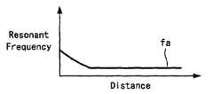
- FIG. 2shows a relationship between a distance from an IC card to a reader/writer and a resonant frequency of a reader/writer.
- the resonant frequency fais almost constant up to a certain point, but it rises when coming close beyond the certain point.
- FIGS. 3 , 4 and 5are diagrams showing examples of states regarding radio communication between an IC card function unit and a reader/writer.
- FIGS. 3A , 4 A and 5 Ashow a carrier waveform transmitted by the reader/writer;
- FIGS. 3B , 4 B and 5 Bshow a response waveform ASK-modulated and
- FIGS. 3C , 4 C and 5 Cshow a composite wave of both waveforms. The composite wave is detected by the reader/writer to receive data transmitted from the IC card.
- FIGS. 3A to 3Cshow the state in which the phase of the response wave from the IC card function unit is the same as that of the carrier wave from the reader/writer.
- FIGS. 5A to 5Cshow the state in which the phase of the response wave from the IC card function unit is reverse to that of the carrier wave from the reader/writer.
- FIGS. 4A to 4Cshow a halfway state regarding the phase difference between the state of FIG. 3 and the state of FIG. 5 .
- FIGS. 3A to 3Cin the case where the phase of the response wave from the IC card function unit is the same as that of the carrier wave from the reader/writer, a change in the level corresponding to the response wave ASK-modulated appears in the composite wave shown in FIG. 3C , and data can be received accurately by the reader/writer. Also, as shown in FIGS. 5A to 5C , in the case where the phase of the response wave from the IC card function unit is reverse to that of the carrier wave from the reader/writer, a change in the level reverse to the response wave ASK-modulated appears in the composite wave shown in FIG. 5 C. Although a change of waveform in this case is reverse to the state of the same phase of FIG. 3 , data can also be received accurately by the reader/writer.
- the statechanges among FIGS. 3 to 5 depending on a distance between an antenna on the IC card side and an antenna on the reader/writer side.
- the state of the same phase that is shown in FIG. 3is obtained.
- the state of the reverse phase that is shown in FIG. 5is obtained.
- the null state shown in FIG. 4occurs at a specific point between the two states.
- FIG. 6shows an example of the relationship between a tuning frequency f 0 of the IC card (tag) and a tuning frequency f 0 of the reader/writer, in which a null area where communication may not be performed occurs in the range of the frequencies being in a certain relationship.
- a reader/writerthat performs radio communication with a radio communication terminal in close proximity thereto, including: an antenna, a demodulating unit, a judging unit and a carrier-wave control unit.
- the antennatransmits a carrier wave of a predetermined frequency and receives a composite wave of the carrier wave and a modulated signal of the carrier wave transmitted from the radio communication terminal.
- the demodulating unitdemodulates the composite wave received by the antenna.
- the judging unitjudges whether or not it is difficult to detect a modulated component included in the composite wave received by the antenna when the radio communication terminal is in close proximity.
- the carrier-wave control unitreduces a component of the carrier wave input into the demodulating unit when the judging unit judges that it is difficult to detect the modulated component.
- the carrier wave that the reader/writer deals withis weakened and consequently the null state is avoided.
- FIG. 1is a diagram showing an example of a system configuration of related art
- FIG. 2is a characteristic curve showing an example of a relationship between a distance from a reader/writer to an IC card and a resonant frequency
- FIGS. 3A to 3Care waveform charts showing a state of communication between a reader/writer and a communicating unit in the case of the same phase;
- FIGS. 4A to 4Care waveform charts showing a state of communication between a reader/writer and a communicating unit in the case of a halfway phase difference;
- FIGS. 5A to 5Care waveform charts showing a state of communication between a reader/writer and a communicating unit in the case of the reverse phase;
- FIG. 6is a frequency characteristic chart showing a range where communication between a reader/writer and a communicating unit is not performed
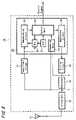
- FIG. 7is a diagram showing a system configuration according to a first embodiment of the present invention.
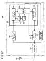
- FIG. 8is a block diagram showing a configuration of a reader/writer according to the first embodiment of the present invention.
- FIG. 9is a block diagram showing a configuration of an auxiliary transmitter according to the first embodiment of the present invention.
- FIGS. 10A to 10Care waveform charts showing re-composite processing according to the first embodiment of the present invention.
- FIG. 11is a block diagram showing a configuration according to a second embodiment of the present invention.
- FIG. 12is a block diagram showing a configuration according to a third embodiment of the present invention.
- a first embodiment of the present inventionis explained in the followings with reference to FIGS. 7 to 10 .
- FIG. 7shows a system configuration in which an RFID unit 51 equivalent to a non-contact IC card function unit is incorporated in a portable terminal 50 .
- the portable terminal 50 of such configurationis brought in close proximity to a reader/writer 10 provided at a predetermined place, and a bidirectional communication with the reader/writer 10 is performed.
- On the reader/writer 10 sideare performed authentication processing for the RFID unit 51 , payment processing and the like.
- a distance with which the communication between the reader/writer 10 and the RFID unit 51 can be performedis a short distance of several to several tens of centimeters.
- an auxiliary transmitter 30is provided at a position adjacent to the reader/writer 10 and a signal of a predetermined frequency is transmitted from an antenna 31 of the auxiliary transmitter 30 in accordance with the communication state detected by the reader/writer 10 .
- the processing and configuration with which a signal is transmitted from the auxiliary transmitter 30are explained later on.
- a carrier wave F 1 (x) of a predetermined frequency(for example, 13.56 MHz) is transmitted from an antenna 11 of the reader/writer 10 to be received by the RFID unit 51 .
- a response wave F 2 (x) to the carrier wave F 1 (x) receivedis prepared in the RFID unit 51 to be transmitted.
- the response wave F 2 (x)is ASK-modulated (amplitude-modulated) based on data regarding authentication, payment settlement or the like.
- a composite wave [F 1 (x)+F 2 (x)]in which the carrier wave F 1 (x) transmitted by itself and the response wave F 2 (x) transmitted from the RFID unit 51 are mixed, is received by the reader/writer 10 .
- each of signals F 1 (x), F 2 (x), F 3 (x)is of the same frequency, and the signal F 3 (x) with which the null state is avoided is a signal that acts on weakening the carrier wave F 1 (x).
- FIG. 8is a diagram showing a specific example of a configuration of the reader/writer 10 .
- a signal received by the antenna 11is supplied to an amplifier/filter 13 through a tuning unit 12 .
- the signalis amplified and filtered in the amplifier/filter 13 to be supplied to a demodulating circuit 21 within a transmitting/receiving block 20 .
- data ASK-modulatedis demodulated from the received signal to be supplied to a control unit 24 .
- a reference-frequency signal synchronized with the received signalis supplied from a PLL (Phase Locked Loop) circuit 22 to the demodulating circuit 21 , and demodulation processing is performed using the reference signal.
- a reference clockis supplied to the PLL circuit 22 from a clock generating unit 23 , and the PLL processing using this clock and the received data is performed.
- the reference clockis also supplied to the control unit 24 and the like in the transmitting/receiving block 20 .
- Transmission data output from the control unit 24is supplied to a modulating circuit 25 . Then, the data is modulated by the carrier wave frequency to be supplied to a driving circuit 14 where a transmission signal with a predetermined output power is prepared.
- the driving circuit 14is connected to the tuning unit 12 and antenna 11 through a resistor 15 , and the transmission signal is wirelessly transmitted from the antenna 11 .
- the tuning unit 12is a circuit tuning a frequency in the antenna 11 to a carrier wave frequency. Further, the resistor 15 of a comparatively small resistance is connected to detect the state of radio communication.
- Voltages at one end (point “a”) and the other end (point “b”) of the resistor 15 connected between the driving circuit 14 and the tuning unit 12are compared in a comparing unit 26 within the transmitting/receiving block 20 , and a difference thereof is judged in the control unit 24 .
- the control unit 24judges that the state of radio communication between the reader/writer 10 and the portable terminal 50 (or IC card) in close proximity thereto has been in the null state (or the state close to the null state) described above.
- the control signalis output to the auxiliary transmitter 30 .
- the control unit 24judges that the voltage becomes a reference voltage value set in advance or less than that, with which a distance from an IC card, portable terminal or the like in close proximity to the reader/writer 10 is estimated. Accordingly, the distance, at which possibility of occurrence of the null state is high, is judged (or estimated) by suitably setting the reference voltage (namely, voltage difference in the comparing unit 26 ). By judging in this way, whether or not it is the null state is judged in the control unit 24 which transmits a control signal that instructs the auxiliary transmitter 30 to transmit the signal F 3 (x) when it is in the null state.
- FIG. 9shows an example of a configuration of the auxiliary transmitter 30 .
- the auxiliary transmitter 30includes a control unit 32 , receiving a control signal transmitted from the reader/writer 10 , generating a signal of a carrier wave frequency in a frequency generating circuit 33 in accordance with contents indicated by the control signal. After being a predetermined transmission power in a driving circuit 34 , the generated signal is supplied to the antenna 31 to be wirelessly transmitted.
- the signal transmitted from the auxiliary transmitter 30becomes the F 3 (x) explained above with reference to FIG. 7 and functions as the signal acting on weakening the carrier wave F 1 (x) when it is in the null state.
- the signal F 3 (x)is of the same frequency as the carrier wave F 1 (x) transmitted from the reader/writer 10
- the signal F 3 (x)is a signal of reverse phase and is the signal whose level is slightly lower than that of the carrier wave F 1 (x).
- FIGS. 10A to 10Can example in which the null state is avoided by the processing of this embodiment is explained with reference to FIGS. 10A to 10C .
- a signal received by the reader/writer 10 during communicationis the composite wave [F 1 (x)+F 2 (x)] in which the carrier wave F 1 (x) transmitted from the reader/writer itself and the response wave F 2 (x) transmitted from the RFID unit are mixed.
- FIG. 10Ashows an example of a waveform of the composite wave [F 1 (x)+F 2 (x)], which shows the null state and there is almost no change in the amplitude.
- the signal F 3 (x) of a carrier wave frequency canceling the occurrence of the null stateis prepared. If there is a transmission of such signal, the signal received consequently by the reader/writer becomes the composite wave [F 1 (x)+F 2 (x)+F 3 (x)] shown in FIG. 10C , in which a signal component of the carrier wave F 1 (x) is weakened and a change in amplitude corresponding to the signal F 2 (x) appears. Hence, data transmitted from the other party can be demodulated.
- the occurrence of the null statecan be avoided by the signal from the auxiliary transmitter arranged in close proximity to the reader/writer 10 , and so the radio communication can be performed favorably between the reader/writer and the RFID side.
- the radio communicationcan favorably be performed with various RFID units.
- This embodimentis also a reader/writer performing short-distance radio communication with an RFID configured with an IC card, portable terminal or the like, in which the null state is avoided by a reader/writer alone.
- FIG. 11is a block diagram showing a configuration of a reader/writer 100 according to this embodiment.
- a signal received by the antenna 101is supplied to an amplifier/filter 103 through a tuning unit 102 .
- the signalis amplified and filtered in the amplifier/filter 103 to be supplied to a demodulating circuit 121 within a transmitting/receiving block 120 .
- data ASK-modulatedis demodulated from the received signal to be supplied to a control unit 124 .
- a reference-frequency signal synchronized with the received signalis supplied to the demodulating circuit 121 from a PLL (Phase Lock Loop) circuit 122 , and demodulation processing is performed using the reference signal.
- a reference clockis supplied to the PLL circuit 122 from a clock generating unit 123 , and the PLL processing using this clock and the received data is performed.
- the reference clockis also supplied to the control unit 124 and the like in the transmitting/receiving block 120 .
- Transmission data output from the control unit 124is supplied to a modulating circuit 125 .
- the datais modulated by the carrier wave frequency to be supplied to a driving circuit 104 where a transmission signal with a predetermined output power is prepared.
- the driving circuit 104is connected to the tuning circuit 102 and antenna 101 , and the transmission signal is wirelessly transmitted from the antenna 101 .
- the reader/writer 100 of this embodimentincludes a null state judging unit 105 which judges whether it is in the null state or not from the signal obtained at a connection point between the driving circuit 104 and tuning unit 102 , or the like. The judged result is supplied to the control unit 124 .
- the null state judging unit 105for example, the resistor 15 and comparing circuit 26 in FIG. 8 explained in the first embodiment can be used.
- the transmitting/receiving block 120includes an F 3 (x) generating circuit 126 and a mixer 127 in which a signal generated in the generating circuit 126 and a received signal output from the amplifier/filter 103 are mixed.
- the signal F 3 (x) generated in the F 3 (x) generating circuit 126is a signal of the same frequency as the carrier wave and of the reverse phase thereto, acting on weakening the carrier wave F 1 (x) explained in the first embodiment.
- the signal F 3 (x)is generated in the F 3 (x) generating circuit 126 by the control of the control unit 124 , being mixed with the received signal in the mixer 127 .
- the signal supplied to the demodulating circuit 121 within the transmitting/receiving block 120becomes a favorable signal in which a change in amplitude appears avoiding the null state, and communication data from the other party can favorably be demodulated.
- the signal shown in FIG. 10A and signal shown in FIG. 10B explained previouslyare mixed in the mixer 127 , and the composite wave shown in FIG. 10C is input into the demodulating circuit 121 . Therefore, favorable short-distance radio communication similar to the above-mentioned first embodiment can be obtained.
- This embodimentis also a reader/writer performing short-distance radio communication with an RFID configured with an IC card, portable terminal or the like, in which the null state is avoided by the processing on the transmission side of the reader/writer.
- FIG. 12is a block diagram showing a configuration of a reader/writer 200 according to this embodiment.
- a signal received by the antenna 201is supplied to an amplifier/filter 203 through a tuning unit 202 .
- the signalis amplified and filtered in the amplifier/filter 203 to be supplied to a demodulating circuit 221 within a transmitting/receiving block 220 .
- data ASK-modulatedis demodulated from the received signal to be supplied to a control unit 224 .
- a reference-frequency signal synchronized with the received signalis supplied to the demodulating circuit 221 from a PLL (Phase Lock Loop) circuit 222 , and demodulation processing is performed using the reference signal.
- a reference clockis supplied to the PLL circuit 222 from a clock generating unit 223 , and the PLL processing using this clock and the received data is performed.
- the reference clockis also supplied to the control unit 224 and the like in the transmitting/receiving block 220 .
- Transmission data output from the control unit 224is supplied to a modulating circuit 225 . Then, the data is modulated by the carrier wave frequency to be supplied to a driving circuit 204 where a transmission signal with a predetermined output power is prepared.
- the driving circuit 204is connected to the tuning circuit 202 and antenna 201 , and the transmission signal is wirelessly transmitted from the antenna 201 .
- the driving circuit 204 of this embodimentcan make the transmission power of the transmission signal weakened by an instruction from the control unit 224 .
- the reader/writer 200 of this embodimentincludes a null state judging unit 205 which judges whether it is in the null state or not from the signal obtained at a connection point between the driving circuit 204 and tuning unit 202 , or the like. The judged result is supplied to the control unit 224 .
- the null state judging unit 205for example, the resistor 15 and comparing circuit 26 in FIG. 8 explained in the first embodiment can be used.
- the transmitting/receiving block 220gives an instruction to weaken a carrier wave component output from the driving circuit 204 and the state of signal wirelessly transmitted from the antenna 201 is changed.
- the processing previously explained of mixing the signal F 3 (x) with the carrier wave F 1 (x)is employed as processing of weakening the carrier wave component.
- the signal received by the reader/writer 200becomes the state shown in FIG. 10C in which the null state is avoided and the composite wave is received to be input into the demodulating circuit 221 . Therefore, favorable short distance radio communication similar to that in the first and second embodiments mentioned above can be performed.
- an embodiment of the present inventioncan be applied to the cases in which an IC card or IC tag is incorporated or attached to a portable terminal other than a mobile phone unit (for example, a portable information processing terminal such as a PDA (Personal Digital Assistance) or the like).
- a portable terminalother than a mobile phone unit
- a portable information processing terminalsuch as a PDA (Personal Digital Assistance) or the like.
Landscapes
- Engineering & Computer Science (AREA)
- Physics & Mathematics (AREA)
- Health & Medical Sciences (AREA)
- Toxicology (AREA)
- Electromagnetism (AREA)
- Theoretical Computer Science (AREA)
- Computer Networks & Wireless Communication (AREA)
- General Physics & Mathematics (AREA)
- Artificial Intelligence (AREA)
- Computer Vision & Pattern Recognition (AREA)
- General Health & Medical Sciences (AREA)
- Signal Processing (AREA)
- Multimedia (AREA)
- Near-Field Transmission Systems (AREA)
Abstract
Description
Claims (6)
Applications Claiming Priority (2)
| Application Number | Priority Date | Filing Date | Title |
|---|---|---|---|
| JP2005-256969 | 2005-09-05 | ||
| JP2005256969AJP4584082B2 (en) | 2005-09-05 | 2005-09-05 | Reader / writer and communication method |
Publications (2)
| Publication Number | Publication Date |
|---|---|
| US20070051809A1 US20070051809A1 (en) | 2007-03-08 |
| US7487921B2true US7487921B2 (en) | 2009-02-10 |
Family
ID=37607003
Family Applications (1)
| Application Number | Title | Priority Date | Filing Date |
|---|---|---|---|
| US11/510,694Expired - Fee RelatedUS7487921B2 (en) | 2005-09-05 | 2006-08-28 | Reader/writer and communication method thereof |
Country Status (6)
| Country | Link |
|---|---|
| US (1) | US7487921B2 (en) |
| EP (2) | EP2284763B1 (en) |
| JP (1) | JP4584082B2 (en) |
| KR (1) | KR20070026196A (en) |
| CN (1) | CN1928885B (en) |
| DE (1) | DE602006017939D1 (en) |
Cited By (17)
| Publication number | Priority date | Publication date | Assignee | Title |
|---|---|---|---|---|
| US20070279002A1 (en)* | 2006-06-01 | 2007-12-06 | Afshin Partovi | Power source, charging system, and inductive receiver for mobile devices |
| US7952322B2 (en) | 2006-01-31 | 2011-05-31 | Mojo Mobility, Inc. | Inductive power source and charging system |
| US8169185B2 (en) | 2006-01-31 | 2012-05-01 | Mojo Mobility, Inc. | System and method for inductive charging of portable devices |
| US8890470B2 (en) | 2010-06-11 | 2014-11-18 | Mojo Mobility, Inc. | System for wireless power transfer that supports interoperability, and multi-pole magnets for use therewith |
| US9106083B2 (en) | 2011-01-18 | 2015-08-11 | Mojo Mobility, Inc. | Systems and method for positioning freedom, and support of different voltages, protocols, and power levels in a wireless power system |
| US9356659B2 (en) | 2011-01-18 | 2016-05-31 | Mojo Mobility, Inc. | Chargers and methods for wireless power transfer |
| US9496732B2 (en) | 2011-01-18 | 2016-11-15 | Mojo Mobility, Inc. | Systems and methods for wireless power transfer |
| US20160372934A1 (en)* | 2015-06-18 | 2016-12-22 | STMicroelectronics (Grand Ouest) SAS | Method for managing contactless power transfer from a transmitter to a receiver, and corresponding transmitter |
| US9722447B2 (en) | 2012-03-21 | 2017-08-01 | Mojo Mobility, Inc. | System and method for charging or powering devices, such as robots, electric vehicles, or other mobile devices or equipment |
| US9755702B2 (en) | 2014-08-04 | 2017-09-05 | Samsung Electronics Co., Ltd. | Method of operating near field communication (NFC) device and NFC device |
| US9837846B2 (en) | 2013-04-12 | 2017-12-05 | Mojo Mobility, Inc. | System and method for powering or charging receivers or devices having small surface areas or volumes |
| US10115520B2 (en) | 2011-01-18 | 2018-10-30 | Mojo Mobility, Inc. | Systems and method for wireless power transfer |
| US11201500B2 (en) | 2006-01-31 | 2021-12-14 | Mojo Mobility, Inc. | Efficiencies and flexibilities in inductive (wireless) charging |
| US11211975B2 (en) | 2008-05-07 | 2021-12-28 | Mojo Mobility, Inc. | Contextually aware charging of mobile devices |
| US11329511B2 (en) | 2006-06-01 | 2022-05-10 | Mojo Mobility Inc. | Power source, charging system, and inductive receiver for mobile devices |
| US11398747B2 (en) | 2011-01-18 | 2022-07-26 | Mojo Mobility, Inc. | Inductive powering and/or charging with more than one power level and/or frequency |
| US11444485B2 (en) | 2019-02-05 | 2022-09-13 | Mojo Mobility, Inc. | Inductive charging system with charging electronics physically separated from charging coil |
Families Citing this family (13)
| Publication number | Priority date | Publication date | Assignee | Title |
|---|---|---|---|---|
| US7431217B2 (en)* | 2004-07-15 | 2008-10-07 | Mastercard International Incorporated | Reference equipment for testing contactless payment devices |
| JP4637204B2 (en) | 2008-04-30 | 2011-02-23 | フェリカネットワークス株式会社 | Communication apparatus and antenna characteristic control method |
| JP2009271775A (en) | 2008-05-08 | 2009-11-19 | Toshiba Corp | Receiving apparatus |
| CN101645129B (en)* | 2008-08-05 | 2013-02-13 | 爱思开电讯投资(中国)有限公司 | Method and device for providing security in near field communication |
| US9766322B2 (en)* | 2013-03-14 | 2017-09-19 | Ensco, Inc. | Geolocation with radio-frequency ranging |
| CN104598854A (en)* | 2015-01-16 | 2015-05-06 | 孟庆国 | Identification card concentrated decoding system |
| US10937019B2 (en)* | 2016-06-08 | 2021-03-02 | Square, Inc. | Wireless communication system with auxiliary antenna |
| US10318953B2 (en) | 2016-06-29 | 2019-06-11 | Square, Inc. | Near field communication flex circuit |
| US10594599B2 (en) | 2016-08-26 | 2020-03-17 | Cisco Technology, Inc. | Fibre channel fabric slow drain mitigation |
| WO2018180149A1 (en)* | 2017-03-29 | 2018-10-04 | 株式会社村田製作所 | Antenna device and electronic instrument |
| US10949189B2 (en) | 2017-06-28 | 2021-03-16 | Square, Inc. | Securely updating software on connected electronic devices |
| US10635820B1 (en) | 2017-09-29 | 2020-04-28 | Square, Inc. | Update policy-based anti-rollback techniques |
| JP6892720B1 (en)* | 2020-12-28 | 2021-06-23 | 吉谷土木株式会社 | Highly efficient recovery system for industrial waste |
Citations (4)
| Publication number | Priority date | Publication date | Assignee | Title |
|---|---|---|---|---|
| US3774209A (en)* | 1970-02-25 | 1973-11-20 | Air Land Systems Co | Radio communication system |
| EP1489684A1 (en) | 2003-06-16 | 2004-12-22 | Sensormatic Electronics Corporation | Antenna system including simultaneous phase aiding and phase canceling element |
| US20060038659A1 (en)* | 2004-08-17 | 2006-02-23 | Fujitsu Limited | Reader/writer and RFID system |
| US7084739B2 (en)* | 2002-06-28 | 2006-08-01 | Brother Kogyo Kabushiki Kaisha | Communication system, and interrogator and transponder for the system |
Family Cites Families (2)
| Publication number | Priority date | Publication date | Assignee | Title |
|---|---|---|---|---|
| JP2003067693A (en)* | 2001-08-27 | 2003-03-07 | Fujitsu Ltd | Non-contact IC card |
| JP3891077B2 (en)* | 2002-09-05 | 2007-03-07 | 株式会社デンソーウェーブ | IC card reader |
- 2005
- 2005-09-05JPJP2005256969Apatent/JP4584082B2/ennot_activeExpired - Fee Related
- 2006
- 2006-08-28USUS11/510,694patent/US7487921B2/ennot_activeExpired - Fee Related
- 2006-08-31KRKR1020060083521Apatent/KR20070026196A/ennot_activeCeased
- 2006-09-04DEDE602006017939Tpatent/DE602006017939D1/enactiveActive
- 2006-09-04EPEP10177544Apatent/EP2284763B1/ennot_activeNot-in-force
- 2006-09-04EPEP06018463Apatent/EP1760629B1/ennot_activeNot-in-force
- 2006-09-05CNCN2006101285808Apatent/CN1928885B/ennot_activeExpired - Fee Related
Patent Citations (4)
| Publication number | Priority date | Publication date | Assignee | Title |
|---|---|---|---|---|
| US3774209A (en)* | 1970-02-25 | 1973-11-20 | Air Land Systems Co | Radio communication system |
| US7084739B2 (en)* | 2002-06-28 | 2006-08-01 | Brother Kogyo Kabushiki Kaisha | Communication system, and interrogator and transponder for the system |
| EP1489684A1 (en) | 2003-06-16 | 2004-12-22 | Sensormatic Electronics Corporation | Antenna system including simultaneous phase aiding and phase canceling element |
| US20060038659A1 (en)* | 2004-08-17 | 2006-02-23 | Fujitsu Limited | Reader/writer and RFID system |
Cited By (54)
| Publication number | Priority date | Publication date | Assignee | Title |
|---|---|---|---|---|
| US11411433B2 (en) | 2006-01-31 | 2022-08-09 | Mojo Mobility, Inc. | Multi-coil system for inductive charging of portable devices at different power levels |
| US11404909B2 (en) | 2006-01-31 | 2022-08-02 | Mojo Mobillity Inc. | Systems for inductive charging of portable devices that include a frequency-dependent shield for reduction of electromagnetic interference and heat during inductive charging |
| US7952322B2 (en) | 2006-01-31 | 2011-05-31 | Mojo Mobility, Inc. | Inductive power source and charging system |
| US8169185B2 (en) | 2006-01-31 | 2012-05-01 | Mojo Mobility, Inc. | System and method for inductive charging of portable devices |
| US8629654B2 (en) | 2006-01-31 | 2014-01-14 | Mojo Mobility, Inc. | System and method for inductive charging of portable devices |
| US11201500B2 (en) | 2006-01-31 | 2021-12-14 | Mojo Mobility, Inc. | Efficiencies and flexibilities in inductive (wireless) charging |
| US11342792B2 (en) | 2006-01-31 | 2022-05-24 | Mojo Mobility, Inc. | System and method for inductive charging of portable devices |
| US11349315B2 (en) | 2006-01-31 | 2022-05-31 | Mojo Mobility, Inc. | System and method for inductive charging of portable devices |
| US12027873B2 (en) | 2006-01-31 | 2024-07-02 | Mojo Mobility Inc. | System and method for inductive charging of portable devices |
| US8947047B2 (en) | 2006-01-31 | 2015-02-03 | Mojo Mobility, Inc. | Efficiency and flexibility in inductive charging |
| US11316371B1 (en) | 2006-01-31 | 2022-04-26 | Mojo Mobility, Inc. | System and method for inductive charging of portable devices |
| US9793721B2 (en) | 2006-01-31 | 2017-10-17 | Mojo Mobility, Inc. | Distributed charging of mobile devices |
| US11462942B2 (en) | 2006-01-31 | 2022-10-04 | Mojo Mobility, Inc. | Efficiencies and method flexibilities in inductive (wireless) charging |
| US11569685B2 (en) | 2006-01-31 | 2023-01-31 | Mojo Mobility Inc. | System and method for inductive charging of portable devices |
| US12040625B2 (en) | 2006-01-31 | 2024-07-16 | Mojo Mobility Inc. | System and method for inductive charging of portable devices |
| US9276437B2 (en) | 2006-01-31 | 2016-03-01 | Mojo Mobility, Inc. | System and method that provides efficiency and flexiblity in inductive charging |
| US9577440B2 (en) | 2006-01-31 | 2017-02-21 | Mojo Mobility, Inc. | Inductive power source and charging system |
| US11121580B2 (en) | 2006-06-01 | 2021-09-14 | Mojo Mobility, Inc. | Power source, charging system, and inductive receiver for mobile devices |
| US11601017B2 (en) | 2006-06-01 | 2023-03-07 | Mojo Mobility Inc. | Power source, charging system, and inductive receiver for mobile devices |
| US7948208B2 (en) | 2006-06-01 | 2011-05-24 | Mojo Mobility, Inc. | Power source, charging system, and inductive receiver for mobile devices |
| US20070279002A1 (en)* | 2006-06-01 | 2007-12-06 | Afshin Partovi | Power source, charging system, and inductive receiver for mobile devices |
| US11329511B2 (en) | 2006-06-01 | 2022-05-10 | Mojo Mobility Inc. | Power source, charging system, and inductive receiver for mobile devices |
| US9461501B2 (en) | 2006-06-01 | 2016-10-04 | Mojo Mobility, Inc. | Power source, charging system, and inductive receiver for mobile devices |
| US8629652B2 (en) | 2006-06-01 | 2014-01-14 | Mojo Mobility, Inc. | Power source, charging system, and inductive receiver for mobile devices |
| US11606119B2 (en) | 2008-05-07 | 2023-03-14 | Mojo Mobility Inc. | Metal layer for inductive power transfer |
| US11211975B2 (en) | 2008-05-07 | 2021-12-28 | Mojo Mobility, Inc. | Contextually aware charging of mobile devices |
| US12278045B2 (en) | 2010-06-11 | 2025-04-15 | Mojo Mobility Inc. | Magnet with multiple opposing poles on a surface for use with magnetically sensitive components |
| US8896264B2 (en) | 2010-06-11 | 2014-11-25 | Mojo Mobility, Inc. | Inductive charging with support for multiple charging protocols |
| US8890470B2 (en) | 2010-06-11 | 2014-11-18 | Mojo Mobility, Inc. | System for wireless power transfer that supports interoperability, and multi-pole magnets for use therewith |
| US8901881B2 (en) | 2010-06-11 | 2014-12-02 | Mojo Mobility, Inc. | Intelligent initiation of inductive charging process |
| US12400779B1 (en) | 2010-06-11 | 2025-08-26 | Mojo Mobility Inc. | Magnetic structure for inductive charging |
| US12293872B2 (en) | 2010-06-11 | 2025-05-06 | Mojo Mobility Inc. | Magnetic structure with multiple opposing poles on a surface for use with magnetically sensitive components |
| US11283306B2 (en) | 2010-06-11 | 2022-03-22 | Mojo Mobility, Inc. | Magnet with multiple opposing poles on a surface for use with magnetically sensitive components |
| US10714986B2 (en) | 2010-06-11 | 2020-07-14 | Mojo Mobility, Inc. | Intelligent initiation of inductive charging process |
| US9112363B2 (en) | 2011-01-18 | 2015-08-18 | Mojo Mobility, Inc. | Intelligent charging of multiple electric or electronic devices with a multi-dimensional inductive charger |
| US9496732B2 (en) | 2011-01-18 | 2016-11-15 | Mojo Mobility, Inc. | Systems and methods for wireless power transfer |
| US9106083B2 (en) | 2011-01-18 | 2015-08-11 | Mojo Mobility, Inc. | Systems and method for positioning freedom, and support of different voltages, protocols, and power levels in a wireless power system |
| US10115520B2 (en) | 2011-01-18 | 2018-10-30 | Mojo Mobility, Inc. | Systems and method for wireless power transfer |
| US11398747B2 (en) | 2011-01-18 | 2022-07-26 | Mojo Mobility, Inc. | Inductive powering and/or charging with more than one power level and/or frequency |
| US9112362B2 (en) | 2011-01-18 | 2015-08-18 | Mojo Mobility, Inc. | Methods for improved transfer efficiency in a multi-dimensional inductive charger |
| US9112364B2 (en) | 2011-01-18 | 2015-08-18 | Mojo Mobility, Inc. | Multi-dimensional inductive charger and applications thereof |
| US12046414B2 (en) | 2011-01-18 | 2024-07-23 | Mojo Mobility Inc. | Powering and/or charging with more than one protocol |
| US9178369B2 (en) | 2011-01-18 | 2015-11-03 | Mojo Mobility, Inc. | Systems and methods for providing positioning freedom, and support of different voltages, protocols, and power levels in a wireless power system |
| US9356659B2 (en) | 2011-01-18 | 2016-05-31 | Mojo Mobility, Inc. | Chargers and methods for wireless power transfer |
| US9722447B2 (en) | 2012-03-21 | 2017-08-01 | Mojo Mobility, Inc. | System and method for charging or powering devices, such as robots, electric vehicles, or other mobile devices or equipment |
| US11929202B2 (en) | 2013-04-12 | 2024-03-12 | Mojo Mobility Inc. | System and method for powering or charging receivers or devices having small surface areas or volumes |
| US11292349B2 (en) | 2013-04-12 | 2022-04-05 | Mojo Mobility Inc. | System and method for powering or charging receivers or devices having small surface areas or volumes |
| US9837846B2 (en) | 2013-04-12 | 2017-12-05 | Mojo Mobility, Inc. | System and method for powering or charging receivers or devices having small surface areas or volumes |
| US11114886B2 (en) | 2013-04-12 | 2021-09-07 | Mojo Mobility, Inc. | Powering or charging small-volume or small-surface receivers or devices |
| US9755702B2 (en) | 2014-08-04 | 2017-09-05 | Samsung Electronics Co., Ltd. | Method of operating near field communication (NFC) device and NFC device |
| US20160372934A1 (en)* | 2015-06-18 | 2016-12-22 | STMicroelectronics (Grand Ouest) SAS | Method for managing contactless power transfer from a transmitter to a receiver, and corresponding transmitter |
| US9991722B2 (en)* | 2015-06-18 | 2018-06-05 | STMicroelectronics (Grand Ouest) SAS | Method for managing contactless power transfer from a transmitter to a receiver, and corresponding transmitter |
| US11811238B2 (en) | 2019-02-05 | 2023-11-07 | Mojo Mobility Inc. | Inductive charging system with charging electronics physically separated from charging coil |
| US11444485B2 (en) | 2019-02-05 | 2022-09-13 | Mojo Mobility, Inc. | Inductive charging system with charging electronics physically separated from charging coil |
Also Published As
| Publication number | Publication date |
|---|---|
| EP2284763B1 (en) | 2012-02-01 |
| EP2284763A1 (en) | 2011-02-16 |
| DE602006017939D1 (en) | 2010-12-16 |
| KR20070026196A (en) | 2007-03-08 |
| JP4584082B2 (en) | 2010-11-17 |
| EP1760629B1 (en) | 2010-11-03 |
| JP2007074153A (en) | 2007-03-22 |
| US20070051809A1 (en) | 2007-03-08 |
| EP1760629A3 (en) | 2007-09-26 |
| CN1928885A (en) | 2007-03-14 |
| CN1928885B (en) | 2011-09-28 |
| EP1760629A2 (en) | 2007-03-07 |
Similar Documents
| Publication | Publication Date | Title |
|---|---|---|
| US7487921B2 (en) | Reader/writer and communication method thereof | |
| EP2031729B1 (en) | Power receiving device and power transfer system | |
| RU2571730C2 (en) | Method and means for data transmission from transponder to reader, primarily in media for payment using mobile communication device | |
| KR20190021281A (en) | Contactless integrated circuit having nfc and uhf operating modes | |
| EP1615158A2 (en) | Non-contact IC card reading/writing apparatus | |
| CN101931531B (en) | Authentication of a terminal-electromagnetic transponder pair by the terminal | |
| US20090291635A1 (en) | Radio-frequency communication device, system and method | |
| US20060220794A1 (en) | Phase modulation for backscatter transponders | |
| CN101937504B (en) | Authentication of a terminal-electromagnetic transponder couple by the transponder | |
| JP2003512801A (en) | Method for reading and writing RFID transponders | |
| CN103597660A (en) | Arrangement of antennas transmitting and receiving an electromagnetic field | |
| CN101359363B (en) | Method for preventing interception in radio frequency recognition system using back-scattering modulation technique | |
| JP4657574B2 (en) | Non-contact IC card reader / writer | |
| JP4463715B2 (en) | Reader / Writer | |
| US7573368B2 (en) | Electromagnetic transponder with no autonomous power supply | |
| Finkenzeller et al. | Range extension of an ISO/IEC 14443 type a RFID system with actively emulating load modulation | |
| EP1542371B1 (en) | Communication system response device | |
| EP1415264B1 (en) | Non-contact smart card interrogator, wherein across a transmission line from an antenna to a receiver the signal modulation varies between amplitude modulation and phase modulation | |
| JP5272802B2 (en) | Non-contact communication device | |
| US20250088833A1 (en) | RF communication device for adaptive detection of further RF communication devices | |
| JP4539469B2 (en) | Communication device | |
| JP2009124546A (en) | Communication apparatus | |
| EP2041692A1 (en) | Transceiver device for responder signals | |
| JP2006245657A (en) | Wireless communication device and non-contact IC card reader / writer device | |
| HK1180089A (en) | Contactless integrated circuit having nfc and uhf operating modes |
Legal Events
| Date | Code | Title | Description |
|---|---|---|---|
| AS | Assignment | Owner name:SONY ERICSSON MOBIL COMMUNICATIONS JAPAN, INC., J Free format text:ASSIGNMENT OF ASSIGNORS INTEREST;ASSIGNORS:TAKAHASHI, TOSHIYUKI;ITO, KUNITAKA;SHIMIZU, KANJIRO;REEL/FRAME:018244/0351 Effective date:20060821 | |
| STCF | Information on status: patent grant | Free format text:PATENTED CASE | |
| FEPP | Fee payment procedure | Free format text:PAYOR NUMBER ASSIGNED (ORIGINAL EVENT CODE: ASPN); ENTITY STATUS OF PATENT OWNER: LARGE ENTITY | |
| FPAY | Fee payment | Year of fee payment:4 | |
| FPAY | Fee payment | Year of fee payment:8 | |
| AS | Assignment | Owner name:SONY MOBILE COMMUNICATIONS JAPAN, INC., JAPAN Free format text:CHANGE OF NAME;ASSIGNOR:SONY ERICSSON MOBILE COMMUNICATIONS JAPAN, INC.;REEL/FRAME:048697/0568 Effective date:20120312 Owner name:SONY MOBILE COMMUNICATIONS, INC., JAPAN Free format text:CHANGE OF NAME;ASSIGNOR:SONY MOBILE COMMUNICATIONS JAPAN, INC.;REEL/FRAME:048698/0713 Effective date:20130107 | |
| AS | Assignment | Owner name:SONY CORPORATION, JAPAN Free format text:ASSIGNMENT OF ASSIGNORS INTEREST;ASSIGNOR:SONY MOBILE COMMUNICATIONS, INC.;REEL/FRAME:050459/0287 Effective date:20190329 | |
| FEPP | Fee payment procedure | Free format text:MAINTENANCE FEE REMINDER MAILED (ORIGINAL EVENT CODE: REM.); ENTITY STATUS OF PATENT OWNER: LARGE ENTITY | |
| LAPS | Lapse for failure to pay maintenance fees | Free format text:PATENT EXPIRED FOR FAILURE TO PAY MAINTENANCE FEES (ORIGINAL EVENT CODE: EXP.); ENTITY STATUS OF PATENT OWNER: LARGE ENTITY | |
| STCH | Information on status: patent discontinuation | Free format text:PATENT EXPIRED DUE TO NONPAYMENT OF MAINTENANCE FEES UNDER 37 CFR 1.362 | |
| FP | Lapsed due to failure to pay maintenance fee | Effective date:20210210 |