US7486867B2 - Methods for forming layers within a MEMS device using liftoff processes to achieve a tapered edge - Google Patents
Methods for forming layers within a MEMS device using liftoff processes to achieve a tapered edgeDownload PDFInfo
- Publication number
- US7486867B2 US7486867B2US11/506,622US50662206AUS7486867B2US 7486867 B2US7486867 B2US 7486867B2US 50662206 AUS50662206 AUS 50662206AUS 7486867 B2US7486867 B2US 7486867B2
- Authority
- US
- United States
- Prior art keywords
- layer
- forming
- mask
- sacrificial
- etch
- Prior art date
- Legal status (The legal status is an assumption and is not a legal conclusion. Google has not performed a legal analysis and makes no representation as to the accuracy of the status listed.)
- Expired - Fee Related, expires
Links
Images


Classifications
- G—PHYSICS
- G02—OPTICS
- G02B—OPTICAL ELEMENTS, SYSTEMS OR APPARATUS
- G02B26/00—Optical devices or arrangements for the control of light using movable or deformable optical elements
- G02B26/08—Optical devices or arrangements for the control of light using movable or deformable optical elements for controlling the direction of light
- G02B26/0816—Optical devices or arrangements for the control of light using movable or deformable optical elements for controlling the direction of light by means of one or more reflecting elements
- G02B26/0833—Optical devices or arrangements for the control of light using movable or deformable optical elements for controlling the direction of light by means of one or more reflecting elements the reflecting element being a micromechanical device, e.g. a MEMS mirror, DMD
- G02B26/0841—Optical devices or arrangements for the control of light using movable or deformable optical elements for controlling the direction of light by means of one or more reflecting elements the reflecting element being a micromechanical device, e.g. a MEMS mirror, DMD the reflecting element being moved or deformed by electrostatic means
- B—PERFORMING OPERATIONS; TRANSPORTING
- B81—MICROSTRUCTURAL TECHNOLOGY
- B81B—MICROSTRUCTURAL DEVICES OR SYSTEMS, e.g. MICROMECHANICAL DEVICES
- B81B3/00—Devices comprising flexible or deformable elements, e.g. comprising elastic tongues or membranes
- B—PERFORMING OPERATIONS; TRANSPORTING
- B81—MICROSTRUCTURAL TECHNOLOGY
- B81B—MICROSTRUCTURAL DEVICES OR SYSTEMS, e.g. MICROMECHANICAL DEVICES
- B81B3/00—Devices comprising flexible or deformable elements, e.g. comprising elastic tongues or membranes
- B81B3/0064—Constitution or structural means for improving or controlling the physical properties of a device
- B81B3/0067—Mechanical properties
- B81B3/0072—For controlling internal stress or strain in moving or flexible elements, e.g. stress compensating layers
- B—PERFORMING OPERATIONS; TRANSPORTING
- B81—MICROSTRUCTURAL TECHNOLOGY
- B81C—PROCESSES OR APPARATUS SPECIALLY ADAPTED FOR THE MANUFACTURE OR TREATMENT OF MICROSTRUCTURAL DEVICES OR SYSTEMS
- B81C1/00—Manufacture or treatment of devices or systems in or on a substrate
- B81C1/00015—Manufacture or treatment of devices or systems in or on a substrate for manufacturing microsystems
- B81C1/00134—Manufacture or treatment of devices or systems in or on a substrate for manufacturing microsystems comprising flexible or deformable structures
- B81C1/00142—Bridges
- B—PERFORMING OPERATIONS; TRANSPORTING
- B81—MICROSTRUCTURAL TECHNOLOGY
- B81C—PROCESSES OR APPARATUS SPECIALLY ADAPTED FOR THE MANUFACTURE OR TREATMENT OF MICROSTRUCTURAL DEVICES OR SYSTEMS
- B81C1/00—Manufacture or treatment of devices or systems in or on a substrate
- B81C1/00642—Manufacture or treatment of devices or systems in or on a substrate for improving the physical properties of a device
- B81C1/0065—Mechanical properties
- B81C1/00666—Treatments for controlling internal stress or strain in MEMS structures
- G—PHYSICS
- G02—OPTICS
- G02B—OPTICAL ELEMENTS, SYSTEMS OR APPARATUS
- G02B26/00—Optical devices or arrangements for the control of light using movable or deformable optical elements
- G02B26/001—Optical devices or arrangements for the control of light using movable or deformable optical elements based on interference in an adjustable optical cavity
- B—PERFORMING OPERATIONS; TRANSPORTING
- B81—MICROSTRUCTURAL TECHNOLOGY
- B81B—MICROSTRUCTURAL DEVICES OR SYSTEMS, e.g. MICROMECHANICAL DEVICES
- B81B2201/00—Specific applications of microelectromechanical systems
- B81B2201/04—Optical MEMS
- B81B2201/047—Optical MEMS not provided for in B81B2201/042 - B81B2201/045
- B—PERFORMING OPERATIONS; TRANSPORTING
- B81—MICROSTRUCTURAL TECHNOLOGY
- B81B—MICROSTRUCTURAL DEVICES OR SYSTEMS, e.g. MICROMECHANICAL DEVICES
- B81B2203/00—Basic microelectromechanical structures
- B81B2203/01—Suspended structures, i.e. structures allowing a movement
- B81B2203/0145—Flexible holders
- B81B2203/0163—Spring holders
- B—PERFORMING OPERATIONS; TRANSPORTING
- B81—MICROSTRUCTURAL TECHNOLOGY
- B81B—MICROSTRUCTURAL DEVICES OR SYSTEMS, e.g. MICROMECHANICAL DEVICES
- B81B2203/00—Basic microelectromechanical structures
- B81B2203/01—Suspended structures, i.e. structures allowing a movement
- B81B2203/019—Suspended structures, i.e. structures allowing a movement characterized by their profile
- B—PERFORMING OPERATIONS; TRANSPORTING
- B81—MICROSTRUCTURAL TECHNOLOGY
- B81B—MICROSTRUCTURAL DEVICES OR SYSTEMS, e.g. MICROMECHANICAL DEVICES
- B81B2203/00—Basic microelectromechanical structures
- B81B2203/03—Static structures
- B81B2203/0307—Anchors
- B—PERFORMING OPERATIONS; TRANSPORTING
- B81—MICROSTRUCTURAL TECHNOLOGY
- B81B—MICROSTRUCTURAL DEVICES OR SYSTEMS, e.g. MICROMECHANICAL DEVICES
- B81B2203/00—Basic microelectromechanical structures
- B81B2203/05—Type of movement
- B81B2203/053—Translation according to an axis perpendicular to the substrate
- B—PERFORMING OPERATIONS; TRANSPORTING
- B81—MICROSTRUCTURAL TECHNOLOGY
- B81C—PROCESSES OR APPARATUS SPECIALLY ADAPTED FOR THE MANUFACTURE OR TREATMENT OF MICROSTRUCTURAL DEVICES OR SYSTEMS
- B81C2201/00—Manufacture or treatment of microstructural devices or systems
- B81C2201/01—Manufacture or treatment of microstructural devices or systems in or on a substrate
- B81C2201/0161—Controlling physical properties of the material
- B81C2201/0163—Controlling internal stress of deposited layers
- B81C2201/0167—Controlling internal stress of deposited layers by adding further layers of materials having complementary strains, i.e. compressive or tensile strain
- Y—GENERAL TAGGING OF NEW TECHNOLOGICAL DEVELOPMENTS; GENERAL TAGGING OF CROSS-SECTIONAL TECHNOLOGIES SPANNING OVER SEVERAL SECTIONS OF THE IPC; TECHNICAL SUBJECTS COVERED BY FORMER USPC CROSS-REFERENCE ART COLLECTIONS [XRACs] AND DIGESTS
- Y10—TECHNICAL SUBJECTS COVERED BY FORMER USPC
- Y10S—TECHNICAL SUBJECTS COVERED BY FORMER USPC CROSS-REFERENCE ART COLLECTIONS [XRACs] AND DIGESTS
- Y10S359/00—Optical: systems and elements
- Y10S359/90—Methods
Definitions
- Microelectromechanical systemsinclude micro mechanical elements, actuators, and electronics. Micromechanical elements may be created using deposition, etching, and/or other micromachining processes that etch away parts of substrates and/or deposited material layers or that add layers to form electrical and electromechanical devices.
- MEMS deviceOne type of MEMS device is called an interferometric modulator.
- interferometric modulator or interferometric light modulatorrefers to a device that selectively absorbs and/or reflects light using the principles of optical interference.
- an interferometric modulatormay comprise a pair of conductive plates, one or both of which may be transparent and/or reflective in whole or part and capable of relative motion upon application of an appropriate electrical signal.
- one platemay comprise a stationary layer deposited on a substrate and the other plate may comprise a metallic membrane separated from the stationary layer by an air gap.
- the position of one plate in relation to anothercan change the optical interference of light incident on the interferometric modulator.
- Such deviceshave a wide range of applications, and it would be beneficial in the art to utilize and/or modify the characteristics of these types of devices so that their features can be exploited in improving existing products and creating new products that have not yet been developed.
- a method of fabricating a MEMS deviceincluding forming an electrode layer over a substrate, forming a sacrificial layer over the electrode layer, patterning the sacrificial layer to form at least one tapered aperture extending through the sacrificial layer, forming a mask layer including an aperture overlying the tapered aperture extending through the sacrificial layer, the mask layer including an overhanging portion extending around the aperture in the mask layer, depositing a support layer over the mask layer, removing the mask layer via a liftoff process, thereby forming a support structure located at least partially within the tapered aperture extending through the sacrificial layer, and forming a movable layer adjacent the support structure.
- a method of fabricating a MEMS deviceincluding forming an electrode layer over a substrate, forming a mask over the electrode layer, where the mask including a negative angle extending about the periphery of the mask, depositing a layer of sacrificial material over the mask, removing the mask via a liftoff process, forming a sacrificial layer including a tapered aperture, forming a support structure located at least partially within the tapered aperture, and forming a movable layer adjacent the support structure.
- a method of fabricating a MEMS deviceincluding forming a lower electrode layer over a substrate, forming a sacrificial layer over the electrode layer, forming a mask layer overlying the sacrificial layer, the mask layer including an aperture having an overhanging portion extending around an edge of the aperture, depositing a layer of electrode material over the mask layer, removing the mask layer via a liftoff process, thereby forming at least an isolated electrode member having an outwardly tapering edge.
- FIG. 1is an isometric view depicting a portion of one embodiment of an interferometric modulator display in which a movable reflective layer of a first interferometric modulator is in a relaxed position and a movable reflective layer of a second interferometric modulator is in an actuated position.
- FIG. 2is a system block diagram illustrating one embodiment of an electronic device incorporating a 3 ⁇ 3 interferometric modulator display.
- FIG. 3is a diagram of movable mirror position versus applied voltage for one exemplary embodiment of an interferometric modulator of FIG. 1 .
- FIG. 4is an illustration of a set of row and column voltages that may be used to drive an interferometric modulator display.
- FIG. 5Aillustrates one exemplary frame of display data in the 3 ⁇ 3 interferometric modulator display of FIG. 2 .
- FIG. 5Billustrates one exemplary timing diagram for row and column signals that may be used to write the frame of FIG. 5A .
- FIGS. 6A and 6Bare system block diagrams illustrating an embodiment of a visual display device comprising a plurality of interferometric modulators.
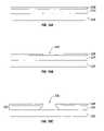
- FIG. 7Ais a cross section of the device of FIG. 1 .
- FIG. 7Bis a cross section of an alternative embodiment of an interferometric modulator.
- FIG. 7Cis a cross section of another alternative embodiment of an interferometric modulator.
- FIG. 7Dis a cross section of yet another alternative embodiment of an interferometric modulator.
- FIG. 7Eis a cross section of an additional alternative embodiment of an interferometric modulator.
- FIG. 8is a top plan view of an array of interferometric modulator elements in which the individual elements comprise support structures.
- FIGS. 9A-9Jare schematic cross-sections illustrating a method for fabricating an interferometric modulator element comprising support structures located over a movable layer.
- FIGS. 10A-10Fare schematic cross-sections illustrating a method for fabricating an interferometric modulator element comprising a reflective layer which is partially separated from a mechanical layer.
- FIGS. 11A-11Bare schematic cross-sections illustrating a method for forming a MEMS structure having a tapered edge through the use of an etch leading layer.
- FIGS. 12A-12Bare schematic cross-sections illustrating an alternate method for forming a MEMS structure having a tapered edge through the use of an etch leading layer.
- FIG. 13is a schematic cross-section illustrating a step in a method for forming a MEMS structure having a tapered edge by altering the properties of the support structure layer during formation of the MEMS structure layer.
- FIG. 14is a schematic cross-section illustrating a step in a method for forming a MEMS structure having a tapered edge by forming a series of sublayers having differing properties to form the MEMS structure layer.
- FIG. 15is a schematic cross-section illustrating a step in a method for forming a MEMS structure having a tapered edge by forming an overlying mask layer having poor adhesion to the MEMS structure layer.
- FIGS. 16A-Dare schematic cross-sections illustrating a method for forming a MEMS structure having a tapered edge through the use of an iterative ashing and etching process.
- FIGS. 17A-17Eare schematic cross-sections illustrating a method for forming a MEMS structure having a tapered edge through the use of multiple etches.
- FIGS. 18A-18Care schematic cross-sections illustrating a method for forming a support structure having tapered edges through the use of a liftoff process.
- FIGS. 19A-19Care schematic cross-sections illustrating a method for forming a mask layer having a negative taper for use in a liftoff process.
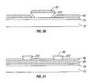
- FIG. 20is a schematic cross-section illustrating a step in a method for forming a sacrificial layer having a tapered aperture.
- FIG. 21is a schematic cross-section illustrating a step in a method for forming an isolated electrode member having a tapered edge.
- the embodimentsmay be implemented in or associated with a variety of electronic devices such as, but not limited to, mobile telephones, wireless devices, personal data assistants (PDAs), hand-held or portable computers, GPS receivers/navigators, cameras, MP3 players, camcorders, game consoles, wrist watches, clocks, calculators, television monitors, flat panel displays, computer monitors, auto displays (e.g., odometer display, etc.), cockpit controls and/or displays, display of camera views (e.g., display of a rear view camera in a vehicle), electronic photographs, electronic billboards or signs, projectors, architectural structures, packaging, and aesthetic structures (e.g., display of images on a piece of jewelry).
- MEMS devices of similar structure to those described hereincan also be used in non-display applications such as in electronic switching devices.
- etching methodscan be used to provide such tapered edges to, e.g., mirror/electrodes or support structures.
- these etching methodsmay include the use of etch leading layers overlying the layers to be etched.
- these etching methodsmay include an iterative etching and/or ashing process.
- liftoff processescan be used to form structures having tapered edges.
- FIG. 1One interferometric modulator display embodiment comprising an interferometric MEMS display element is illustrated in FIG. 1 .
- the pixelsare in either a bright or dark state.
- the display elementIn the bright (“on” or “open”) state, the display element reflects a large portion of incident visible light to a user.
- the dark (“off” or “closed”) stateWhen in the dark (“off” or “closed”) state, the display element reflects little incident visible light to the user.
- the light reflectance properties of the “on” and “off” statesmay be reversed.
- MEMS pixelscan be configured to reflect predominantly at selected colors, allowing for a color display in addition to black and white.
- FIG. 1is an isometric view depicting two adjacent pixels in a series of pixels of a visual display, wherein each pixel comprises a MEMS interferometric modulator.
- an interferometric modulator displaycomprises a row/column array of these interferometric modulators.
- Each interferometric modulatorincludes a pair of reflective layers positioned at a variable and controllable distance from each other to form a resonant optical cavity with at least one variable dimension.
- one of the reflective layersmay be moved between two positions. In the first position, referred to herein as the relaxed position, the movable reflective layer is positioned at a relatively large distance from a fixed partially reflective layer.
- the movable reflective layerIn the second position, referred to herein as the actuated position, the movable reflective layer is positioned more closely adjacent to the partially reflective layer. Incident light that reflects from the two layers interferes constructively or destructively depending on the position of the movable reflective layer, producing either an overall reflective or non-reflective state for each pixel.
- the depicted portion of the pixel array in FIG. 1includes two adjacent interferometric modulators 12 a and 12 b .
- a movable reflective layer 14 ais illustrated in a relaxed position at a predetermined distance from an optical stack 16 a , which includes a partially reflective layer.
- the movable reflective layer 14 bis illustrated in an actuated position adjacent to the optical stack 16 b.
- optical stack 16typically comprise several fused layers, which can include an electrode layer, such as indium tin oxide (ITO), a partially reflective layer, such as chromium, and a transparent dielectric.
- ITOindium tin oxide
- the optical stack 16is thus electrically conductive, partially transparent, and partially reflective, and may be fabricated, for example, by depositing one or more of the above layers onto a transparent substrate 20 .
- the partially reflective layercan be formed from a variety of materials that are partially reflective such as various metals, semiconductors, and dielectrics.
- the partially reflective layercan be formed of one or more layers of materials, and each of the layers can be formed of a single material or a combination of materials.
- the layers of the optical stack 16are patterned into parallel strips, and may form row electrodes in a display device as described further below.
- the movable reflective layers 14 a , 14 bmay be formed as a series of parallel strips of a deposited metal layer or layers (orthogonal to the row electrodes of 16 a , 16 b ) deposited on top of posts 18 and an intervening sacrificial material deposited between the posts 18 . When the sacrificial material is etched away, the movable reflective layers 14 a , 14 b are separated from the optical stacks 16 a , 16 b by a defined gap 19 .
- a highly conductive and reflective materialsuch as aluminum may be used for the reflective layers 14 , and these strips may form column electrodes in a display device.
- the cavity 19remains between the movable reflective layer 14 a and optical stack 16 a , with the movable reflective layer 14 a in a mechanically relaxed state, as illustrated by the pixel 12 a in FIG. 1 .
- a potential differenceis applied to a selected row and column, the capacitor formed at the intersection of the row and column electrodes at the corresponding pixel becomes charged, and electrostatic forces pull the electrodes together.
- the movable reflective layer 14is deformed and is forced against the optical stack 16 .
- a dielectric layerwithin the optical stack 16 may prevent shorting and control the separation distance between layers 14 and 16 , as illustrated by pixel 12 b on the right in FIG. 1 .
- the behavioris the same regardless of the polarity of the applied potential difference. In this way, row/column actuation that can control the reflective vs. non-reflective pixel states is analogous in many ways to that used in conventional LCD and other display technologies.
- FIGS. 2 through 5Billustrate one exemplary process and system for using an array of interferometric modulators in a display application.
- FIG. 2is a system block diagram illustrating one embodiment of an electronic device that may incorporate aspects of the invention.
- the electronic deviceincludes a processor 21 which may be any general purpose single- or multi-chip microprocessor such as an ARM, Pentium®, Pentium II®, Pentium III®, Pentium IV®, Pentium® Pro, an 8051, a MIPS®, a Power PC®, an ALPHA®, or any special purpose microprocessor such as a digital signal processor, microcontroller, or a programmable gate array.
- the processor 21may be configured to execute one or more software modules.
- the processormay be configured to execute one or more software applications, including a web browser, a telephone application, an email program, or any other software application.
- the processor 21is also configured to communicate with an array driver 22 .
- the array driver 22includes a row driver circuit 24 and a column driver circuit 26 that provide signals to a display array or panel 30 .
- the cross section of the array illustrated in FIG. 1is shown by the lines 1 - 1 in FIG. 2 .
- the row/column actuation protocolmay take advantage of a hysteresis property of these devices illustrated in FIG. 3 . It may require, for example, a 10 volt potential difference to cause a movable layer to deform from the relaxed state to the actuated state. However, when the voltage is reduced from that value, the movable layer maintains its state as the voltage drops back below 10 volts.
- the movable layerdoes not relax completely until the voltage drops below 2 volts.
- a window of applied voltageabout 3 to 7 V in the example illustrated in FIG. 3 , within which the device is stable in either the relaxed or actuated state. This is referred to herein as the “hysteresis window” or “stability window.”
- the row/column actuation protocolcan be designed such that during row strobing, pixels in the strobed row that are to be actuated are exposed to a voltage difference of about 10 volts, and pixels that are to be relaxed are exposed to a voltage difference of close to zero volts.
- each pixelsees a potential difference within the “stability window” of 3-7 volts in this example.
- This featuremakes the pixel design illustrated in FIG. 1 stable under the same applied voltage conditions in either an actuated or relaxed pre-existing state. Since each pixel of the interferometric modulator, whether in the actuated or relaxed state, is essentially a capacitor formed by the fixed and moving reflective layers, this stable state can be held at a voltage within the hysteresis window with almost no power dissipation. Essentially no current flows into the pixel if the applied potential is fixed.
- a display framemay be created by asserting the set of column electrodes in accordance with the desired set of actuated pixels in the first row.
- a row pulseis then applied to the row 1 electrode, actuating the pixels corresponding to the asserted column lines.
- the asserted set of column electrodesis then changed to correspond to the desired set of actuated pixels in the second row.
- a pulseis then applied to the row 2 electrode, actuating the appropriate pixels in row 2 in accordance with the asserted column electrodes.
- the row 1 pixelsare unaffected by the row 2 pulse, and remain in the state they were set to during the row 1 pulse. This may be repeated for the entire series of rows in a sequential fashion to produce the frame.
- the framesare refreshed and/or updated with new display data by continually repeating this process at some desired number of frames per second.
- protocols for driving row and column electrodes of pixel arrays to produce display framesare also well known and may be used in conjunction with the present invention.
- FIGS. 4 , 5 A, and 5 Billustrate one possible actuation protocol for creating a display frame on the 3 ⁇ 3 array of FIG. 2 .
- FIG. 4illustrates a possible set of column and row voltage levels that may be used for pixels exhibiting the hysteresis curves of FIG. 3 .
- actuating a pixelinvolves setting the appropriate column to ⁇ V bias , and the appropriate row to + ⁇ V, which may correspond to ⁇ 5 volts and +5 volts, respectively Relaxing the pixel is accomplished by setting the appropriate column to +V bias , and the appropriate row to the same + ⁇ V, producing a zero volt potential difference across the pixel.
- the pixelsare stable in whatever state they were originally in, regardless of whether the column is at +V bias , or ⁇ V bias .
- voltages of opposite polarity than those described abovecan be used, e.g., actuating a pixel can involve setting the appropriate column to +V bias , and the appropriate row to ⁇ V.
- releasing the pixelis accomplished by setting the appropriate column to ⁇ V bias , and the appropriate row to the same ⁇ V, producing a zero volt potential difference across the pixel.
- FIG. 5Bis a timing diagram showing a series of row and column signals applied to the 3 ⁇ 3 array of FIG. 2 which will result in the display arrangement illustrated in FIG. 5A , where actuated pixels are non-reflective.
- the pixelsPrior to writing the frame illustrated in FIG. 5A , the pixels can be in any state, and in this example, all the rows are at 0 volts, and all the columns are at +5 volts. With these applied voltages, all pixels are stable in their existing actuated or relaxed states.
- pixels ( 1 , 1 ), ( 1 , 2 ), ( 2 , 2 ), ( 3 , 2 ) and ( 3 , 3 )are actuated.
- columns 1 and 2are set to ⁇ 5 volts
- column 3is set to +5 volts. This does not change the state of any pixels, because all the pixels remain in the 3-7 volt stability window.
- Row 1is then strobed with a pulse that goes from 0, up to 5 volts, and back to zero. This actuates the ( 1 , 1 ) and ( 1 , 2 ) pixels and relaxes the ( 1 , 3 ) pixel. No other pixels in the array are affected.
- row 2is set to ⁇ 5 volts, and columns 1 and 3 are set to +5 volts.
- the same strobe applied to row 2will then actuate pixel ( 2 , 2 ) and relax pixels ( 2 , 1 ) and ( 2 , 3 ). Again, no other pixels of the array are affected.
- Row 3is similarly set by setting columns 2 and 3 to ⁇ 5 volts, and column 1 to +5 volts.
- the row 3strobe sets the row 3 pixels as shown in FIG. 5A . After writing the frame, the row potentials are zero, and the column potentials can remain at either +5 or ⁇ 5 volts, and the display is then stable in the arrangement of FIG. 5A .
- FIGS. 6A and 6Bare system block diagrams illustrating an embodiment of a display device 40 .
- the display device 40can be, for example, a cellular or mobile telephone.
- the same components of display device 40 or slight variations thereofare also illustrative of various types of display devices such as televisions and portable media players.
- the display device 40includes a housing 41 , a display 30 , an antenna 43 , a speaker 45 , an input device 48 , and a microphone 46 .
- the housing 41is generally formed from any of a variety of manufacturing processes as are well known to those of skill in the art, including injection molding and vacuum forming.
- the housing 41may be made from any of a variety of materials, including, but not limited to, plastic, metal, glass, rubber, and ceramic, or a combination thereof.
- the housing 41includes removable portions (not shown) that may be interchanged with other removable portions of different color, or containing different logos, pictures, or symbols.
- the display 30 of the exemplary display device 40may be any of a variety of displays, including a bi-stable display, as described herein.
- the display 30includes a flat-panel display, such as plasma, EL, OLED, STN LCD, or TFT LCD as described above, or a non-flat-panel display, such as a CRT or other tube device, as is well known to those of skill in the art.
- the display 30includes an interferometric modulator display, as described herein.
- the components of one embodiment of the exemplary display device 40are schematically illustrated in FIG. 6B .
- the illustrated exemplary display device 40includes a housing 41 and can include additional components at least partially enclosed therein.
- the exemplary display device 40includes a network interface 27 that includes an antenna 43 , which is coupled to a transceiver 47 .
- the transceiver 47is connected to a processor 21 , which is connected to conditioning hardware 52 .
- the conditioning hardware 52may be configured to condition a signal (e.g., filter a signal).
- the conditioning hardware 52is connected to a speaker 45 and a microphone 46 .
- the processor 21is also connected to an input device 48 and a driver controller 29 .
- the driver controller 29is coupled to a frame buffer 28 and to an array driver 22 , which in turn is coupled to a display array 30 .
- a power supply 50provides power to all components as required by the particular exemplary display device 40 design.
- the network interface 27includes the antenna 43 and the transceiver 47 so that the exemplary display device 40 can communicate with one or more devices over a network. In one embodiment, the network interface 27 may also have some processing capabilities to relieve requirements of the processor 21 .
- the antenna 43is any antenna known to those of skill in the art for transmitting and receiving signals. In one embodiment, the antenna transmits and receives RF signals according to the IEEE 802.11 standard, including IEEE 802.11(a), (b), or (g). In another embodiment, the antenna transmits and receives RF signals according to the BLUETOOTH standard. In the case of a cellular telephone, the antenna is designed to receive CDMA, GSM, AMPS, or other known signals that are used to communicate within a wireless cell phone network.
- the transceiver 47pre-processes the signals received from the antenna 43 so that they may be received by and further manipulated by the processor 21 .
- the transceiver 47also processes signals received from the processor 21 so that they may be transmitted from the exemplary display device 40 via the antenna 43 .
- the transceiver 47can be replaced by a receiver.
- the network interface 27can be replaced by an image source, which can store or generate image data to be sent to the processor 21 .
- the image sourcecan be memory device such as a digital video disc (DVD) or a hard-disc drive that contains image data, or a software module that generates image data.
- the processor 21generally controls the overall operation of the exemplary display device 40 .
- the processor 21receives data, such as compressed image data from the network interface 27 or an image source, and processes the data into raw image data or into a format that is readily processed into raw image data.
- the processor 21then sends the processed data to the driver controller 29 or to the frame buffer 28 for storage.
- Raw datatypically refers to the information that identifies the image characteristics at each location within an image. For example, such image characteristics can include color, saturation, and gray-scale level.
- the processor 21includes a microcontroller, CPU, or logic unit to control operation of the exemplary display device 40 .
- the conditioning hardware 52generally includes amplifiers and filters for transmitting signals to the speaker 45 , and for receiving signals from the microphone 46 .
- the conditioning hardware 52may be discrete components within the exemplary display device 40 , or may be incorporated within the processor 21 or other components.
- the driver controller 29takes the raw image data generated by the processor 21 either directly from the processor 21 or from the frame buffer 28 and reformats the raw image data appropriately for high speed transmission to the array driver 22 . Specifically, the driver controller 29 reformats the raw image data into a data flow having a raster-like format, such that it has a time order suitable for scanning across the display array 30 . Then the driver controller 29 sends the formatted information to the array driver 22 .
- a driver controller 29such as a LCD controller, is often associated with the system processor 21 as a stand-alone Integrated Circuit (IC), such controllers may be implemented in many ways. They may be embedded in the processor 21 as hardware, embedded in the processor 21 as software, or fully integrated in hardware with the array driver 22 .
- the array driver 22receives the formatted information from the driver controller 29 and reformats the video data into a parallel set of waveforms that are applied many times per second to the hundreds and sometimes thousands of leads coming from the display's x-y matrix of pixels.
- the driver controller 29 , the array driver 22 , and the display array 30are appropriate for any of the types of displays described herein.
- the driver controller 29is a conventional display controller or a bi-stable display controller (e.g., an interferometric modulator controller).
- the array driver 22is a conventional driver or a bi-stable display driver (e.g., an interferometric modulator display).
- a driver controller 29is integrated with the array driver 22 .
- the display array 30is a typical display array or a bi-stable display array (e.g., a display including an array of interferometric modulators).
- the input device 48allows a user to control the operation of the exemplary display device 40 .
- the input device 48includes a keypad, such as a QWERTY keyboard or a telephone keypad, a button, a switch, a touch-sensitive screen, or a pressure- or heat-sensitive membrane.
- the microphone 46is an input device for the exemplary display device 40 . When the microphone 46 is used to input data to the device, voice commands may be provided by a user for controlling operations of the exemplary display device 40 .
- the power supply 50can include a variety of energy storage devices as are well known in the art.
- the power supply 50is a rechargeable battery, such as a nickel-cadmium battery or a lithium ion battery.
- the power supply 50is a renewable energy source, a capacitor, or a solar cell including a plastic solar cell, and solar-cell paint.
- the power supply 50is configured to receive power from a wall outlet.
- control programmabilityresides, as described above, in a driver controller which can be located in several places in the electronic display system. In some embodiments, control programmability resides in the array driver 22 . Those of skill in the art will recognize that the above-described optimizations may be implemented in any number of hardware and/or software components and in various configurations.
- FIGS. 7A-7Eillustrate five different embodiments of the movable reflective layer 14 and its supporting structures.
- FIG. 7Ais a cross section of the embodiment of FIG. 1 , where a strip of metal material 14 is deposited on orthogonally extending supports 18 .
- FIG. 7Bthe moveable reflective layer 14 is attached to supports 18 at the corners only, on tethers 32 .
- FIG. 7Cthe moveable reflective layer 14 is suspended from a deformable layer 34 , which may comprise a flexible metal.
- the deformable layer 34connects, directly or indirectly, to the substrate 20 around the perimeter of the deformable layer 34 .
- connection structureswhich can take the form of isolated pillars or posts and/or continuous walls or rails.
- the embodiment illustrated in FIG. 7Dhas support structures 18 that include support plugs 42 upon which the deformable layer 34 rests.
- the movable reflective layer 14remains suspended over the cavity, as in FIGS. 7A-7C , but the deformable layer 34 does not form the support posts by filling holes between the deformable layer 34 and the optical stack 16 . Rather, the support posts 18 are formed of a planarization material, which is used to form the support post plugs 42 .
- the embodiment illustrated in FIG. 7Eis based on the embodiment shown in FIG. 7D , but may also be adapted to work with any of the embodiments illustrated in FIGS.
- FIG. 7Ean extra layer of metal or other conductive material has been used to form a bus structure 44 . This allows signal routing along the back of the interferometric modulators, eliminating a number of electrodes that may otherwise have had to be formed on the substrate 20 .
- the interferometric modulatorsfunction as direct-view devices, in which images are viewed from the front side of the transparent substrate 20 , the side opposite to that upon which the modulator is arranged.
- the reflective layer 14optically shields the portions of the interferometric modulator on the side of the reflective layer opposite the substrate 20 , including the deformable layer 34 . This allows the shielded areas to be configured and operated upon without negatively affecting the image quality.
- Such shieldingallows the bus structure 44 in FIG. 7E , which provides the ability to separate the optical properties of the modulator from the electromechanical properties of the modulator, such as addressing and the movements that result from that addressing.
- This separable modulator architectureallows the structural design and materials used for the electromechanical aspects and the optical aspects of the modulator to be selected and to function independently of each other.
- the embodiments shown in FIGS. 7C-7Ehave additional benefits deriving from the decoupling of the optical properties of the reflective layer 14 from its mechanical properties, which are carried out by the deformable layer 34 .
- Thisallows the structural design and materials used for the reflective layer 14 to be optimized with respect to the optical properties, and the structural design and materials used for the deformable layer 34 to be optimized with respect to desired mechanical properties.
- a movable layersuch as the movable reflective layer 14 illustrated in FIG. 7A , or the combination of mechanical layer 34 and movable reflective layer 14 of FIGS. 7C-7E .
- the movable layermay comprise a reflective sublayer and a mechanical sublayer, as will be discussed in greater detail below.
- Such supportmay be provided by a series of support structures which may be located along the edges of an individual modulator element and/or in the interior of such an element. In various embodiments, these support structures may be located either over or underneath a movable layer.
- support structuresmay extend through an aperture formed in the mechanical layer, such that support is provided from both above and below the mechanical layer.
- the term “rivet”generally refers to a patterned layer overlying a mechanical layer in a MEMS device, usually in a recess or depression in the post or support region, to lend mechanical support for the mechanical layer.
- the rivetincludes wings overlying an upper surface of the mechanical layer to add stability and predictability to the mechanical layer's movement.
- support structures underlying a mechanical layer in a MEMS device to lend mechanical support for the mechanical layerare generally referred to herein as support “posts.”
- the preferred materialsare inorganic for stability relative to organic resist materials.
- FIG. 8depicts an array of MEMS elements.
- the arraymay comprise an array of interferometric modulators, but in alternate embodiments, the MEMS elements may comprise any MEMS device having a movable layer.
- support structures 62which in the illustrated embodiment are underlying post structures but may in other embodiments include overlying rivet structures, are located both along the edges of a movable layer 66 and in the interior of a MEMS element, in this example an interferometric modulator element 60 .
- Certain support structuresmay comprise rail structures 64 , which extend across the gap 65 between two adjacent movable layers 66 .
- movable layer 66comprises a strip of deformable material extending through multiple adjacent elements 60 within the same column.
- the rail structures 64run parallel with lower electrodes which define rows crossing the upper electrodes defined by the strips of the movable layer 66 .
- the support structures 62serve to stiffen the movable layer 66 within the elements or pixels 60 , and together with the rail structures 64 , separate the upper and lower electrodes to define cavities in which the upper electrode can move vertically.
- these support structures 62are made small relative to the surrounding area of the modulator element 60 .
- the support postsconstrain deflection of the movable layer 66 and may generally be opaque, the area underneath and immediately surrounding the support structures 62 is not usable as active area in a display, as the movable layer in those areas is not movable to a fully actuated position (e.g., one in which a portion of the lower surface of the movable layer 14 of FIG. 7A is in contact with the upper surface of the optical stack 16 ). Because this may result in undesirable optical effects in the areas surrounding the post, a dark or “black” mask layer may advantageously be provided between the support structures and the viewer to avoid excessive reflection in these regions that may wash out the intended color.
- these support structuresmay comprise a depression in the movable layer, along with a substantially rigid structure(s) above and/or below the movable layer which helps to maintain the shape. While such support structures may be formed of a polymer material, an inorganic material having greater rigidity is preferably used, and provides advantages over similar structures comprising polymeric materials.
- a polymeric support structuremay not maintain a desired level of rigidity over a wide range of operating temperatures, and may be subject to gradual deformation or mechanical failure over the lifetime of a device.
- failuresmay affect the distance between the movable layer and the optical stack, and this distance at least partially determines the wavelengths reflected by the interferometric modulator element, such failures may lead to a shift in the reflected color due to wear over time or variance in operating temperatures.
- Other MEMS devicesexperience analogous degradation over time when supports are formed of polymeric material.
- FIGS. 9A-9JOne process for forming an interferometric modulator element comprising underlying post support structures is described with respect to FIGS. 9A-9J .
- a transparent or light-transmissive substrate 70is provided, which may comprise, for example, glass or a transparent polymeric material.
- a conductive layer 72which may comprise indium-tin-oxide (ITO), is then deposited over the transparent substrate and a partially reflective layer 74 , which may comprise chromium, is deposited over the conductive layer 72 .
- ITOindium-tin-oxide
- conductive layer 72may comprise ITO, and may be referred to as such at various points in the below specification, it will be understood that the conductive layer 72 may comprise any suitable conductive material, and need not be transparent for non-optical MEMS structures.
- partially reflective layer 74may comprise any suitable partially reflective layer, and may be omitted for non-optical MEMS structures.
- the conductive layer 72 and partially reflective layer 74are then patterned and etched to form bottom electrodes, also referred to as row electrodes, which run cross-wise (e.g., perpendicular) to the movable layer 66 of FIG. 8 and which will be used to address a row of MEMS elements.
- the conductive and partially reflective layers 72 and 74may advantageously also be patterned and etched to remove the ITO and chromium underlying the areas where the support post structures will be located, forming apertures 76 as depicted in FIG. 9B . This patterning and etching is preferably done by the same process which forms the row electrodes.
- FIG. 9B and the subsequent figuresdepict a cross-section of a continuous row electrode formed by layers 72 and 74 , in which isolated apertures 76 have been etched, taken along a line extending through those apertures.
- a dielectric layerdiscussed below, may provide sufficient protection against shorting between the bottom electrode and the movable layer.
- the conductive layer 72 and partially reflective layer 74may be patterned via photolithography and etched via, for example, commercially available wet etches.
- Chromium wet etchesinclude solutions of acetic acid (C 2 H 4 O 2 ) and cerium ammonium nitrate [Ce(NH 4 ) 2 (NO 3 ) 6 ].
- ITO wet etchesinclude HCl, a mixture of HCl and HNO 3 , or a mixture of FeCl 3 /HCl/DI in a 75%/3%/22% ratio and H 2 O.
- a dielectric layer 78is deposited over the conductive and partially reflective layers 72 and 74 , as seen in FIG. 9C , forming the optical stack 16 .
- the dielectric layermay comprise SiO 2 or SiN x , although a wide variety of suitable materials may be used.
- the thickness and positioning of the layers forming the optical stack 16determines the color reflected by the interferometric modulator element when the element is actuated (collapsed), bringing the movable layer 66 into contact with the optical stack.
- the optical stackis configured such that the interferometric modulator element reflects substantially no visible light (appears black) when the movable layer is in an actuated position.
- the thickness of the dielectric layer 78is about 450 ⁇ , although it will be understood that the desired thickness will vary based on both the refractive index of the material and the desired color reflected by the interferometric modulator in a collapsed state. While illustrated for simplicity as planar (which can be achieved if the dielectric layer 78 is a spin-on glass), the dielectric layer 78 is typically conformal over the patterned lower electrode formed from layers 72 and 74 .
- a layer 82 of sacrificial materialis then deposited over the dielectric layer 78 .
- this sacrificial layer 82is formed from a material which is etchable by fluorine-based etchants, particularly XeF 2 .
- the sacrificial layer 82may be formed from molybdenum or amorphous silicon (a-Si).
- the sacrificial layermay comprise tantalum or tungsten.
- Other materials which are usable as sacrificial materialsinclude silicon nitride, certain oxides, and organic materials.
- the thickness of the deposited sacrificial layer 82will determine the distance between the optical stack 16 and the movable layer 66 , thus defining the dimensions of the interferometric gap 19 (see FIG. 7A ). As the height of the gap 19 determines the color reflected by the interferometric modulator element when in an unactuated position, the thickness of the sacrificial layer 82 will vary depending on the desired characteristics of the interferometric modulator. For instance, in an embodiment in which a modulator element that reflects green in the unactuated position is formed, the thickness of the sacrificial layer 82 may be roughly 2000 ⁇ . In further embodiments, the sacrificial layer may have multiple thicknesses across an array of MEMS devices, such as in a multicolor display system where different interferometric gap sizes are used to produce different colors.
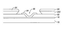
- the sacrificial layer 82has been patterned and etched to form tapered apertures 86 .
- the apertures 86overlie the apertures 76 cut into the layers 72 and 74 of ITO and chromium.
- These apertures 86may be formed by masking the sacrificial layer, using photolithography, and then performing either a wet or dry etch to remove portions of the sacrificial material. Suitable dry etches include, but are not limited to, SF 6 , CF 4 , Cl 2 , or any mixture of these gases with O 2 or a noble gas such as He or Ar.
- Wet etches suitable for etching Moinclude a PAN etch, which may be a mix of phosphoric acid, acetic acid, nitric acid and deionized water in a 16:1:1:2 ratio.
- Amorphous siliconcan be etched by wet etches including KOH and HF Nitrate.
- a dry etchis used to etch the sacrificial layer 82 , as dry etches permit more control over the shape of tapered apertures 86 .
- a layer 84 of inorganic post materialis deposited over the patterned sacrificial layer 82 , such that the inorganic post layer 84 also coats the side walls and the base of the tapered apertures 86 .
- the inorganic post layer 84is thinner than the sacrificial layer 82 , and is conformal over the sacrificial layer 82 .
- the inorganic post layer 84may comprise silicon nitride (SiN x ) or SiO 2 , although a wide variety of other materials may be used, some of which are discussed in greater detail below.
- the inorganic post layer 84is patterned and etched to form inorganic posts 88 .
- the inorganic post layer 84is preferably selectively etchable with respect to the underlying sacrificial layer 82 , so as to permit etching of inorganic post layer 84 while leaving the sacrificial layer 82 unaffected.
- an etch stop layer(not shown) may be provided between the inorganic post layer 84 and the sacrificial layer 82 .
- the edges of the inorganic posts 88preferably taper which, like the tapered or sloped sidewalls of the apertures 86 , facilitates continuous and conformal deposition of overlying layers.
- the post structure 88 in the illustrated embodimenthas a thickness which is thinner than that of the sacrificial layer 82 , and comprises a substantially flat base portion 89 , a sloped sidewall portion 87 , and a substantially horizontal wing portion 85 which extends over a portion of the sacrificial material.
- the post 88advantageously provides a substantially flat surface at the edge of the post for supporting an overlying movable layer 66 (see FIG.
- the inorganic post layer 84 and resultant post 88comprise diamond-like carbon (DLC).
- DLCdiamond-like carbon
- the DLC inorganic post layer 84can be etched with an O 2 dry etch.
- an O 2 dry etchis highly selective relative to a wide variety of sacrificial materials, including but not limited to Mo and a-Si sacrificial material, as well as other sacrificial materials discussed above.
- An inorganic post comprising DLCthus provides a very stiff post, lessening the likelihood and amount of downward flexure of the edges of the support post 88 when overlying moving or mechanical layers are pulled downward during MEMS operation, while permitting the use of an etch which is relatively benign to a wide variety of materials.
- FIG. 9Hit can be seen that the components which will form the movable layer 66 (see, e.g., moveable reflective layer 14 in FIG. 7A ) are then deposited over the etched sacrificial layer 82 , lining the tapered apertures 86 .
- a highly reflective layer 90also referred to as a mirror or mirror layer, is deposited first, followed by a mechanical layer 92 .
- the highly reflective layer 90may be formed from a specular metal, such as aluminum or an aluminum alloy, due to their high reflectance over a wide spectrum of wavelengths.
- the mechanical layer 92may comprise a metal such as Ni and Cr, and is preferably formed such that the mechanical layer 92 contains residual tensile stress.
- the residual tensile stressprovides the mechanical force which tend to pull the movable layer 66 away from the optical stack 16 when the modulator is unactuated, or “relaxed.”
- the combination of the highly reflective layer 90 and mechanical layer 92is collectively referred to as the movable layer 66 , although it will be understood that the term movable layer, as used herein, also encompasses a partially separated mechanical and reflective layer, such as the mechanical layer 34 and the movable reflective layer 14 of FIG. 7C .
- both the reflective layer 90 and the mechanical layer 92are preferably resistant to XeF 2 etching. If either of these layers is not resistant, an etch stop layer may be used to protect the non-resistant layer surface exposed to the release etch.
- the post 88is preferably resistant to the release etch, or is alternately protected by an etch stop layer. It can also be seen that the taper of the edges of the posts 88 facilitates the conformal deposition of the reflective layer 90 and mechanical layer 92 . Absent this taper, it may be difficult to deposit these layers such that the layers have substantially uniform thicknesses over surfaces outside and within the apertures 86 .
- the movable layer 66may be a single layer which is both highly reflective and has the desired mechanical characteristics. However, the deposition of two distinct layers permits the selection of a highly reflective material, which might otherwise be unsuitable if used as the sole material in a movable layer 66 , and similarly allows selection of a suitable mechanical layer (with some flexibility and inherent tension) without regard to its reflective properties.
- the movable layermay be a reflective sublayer which is largely detached from the electrical and mechanical layer, such that the reflective layer may be translated vertically without bending (see, e.g., FIGS. 10A-10F and attendant description).
- the MEMS devices being formedcomprise non-optical MEMS devices (e.g., a MEMS switch)
- the movable layer 66need not comprise a reflective material.
- the underside of the movable layer 66need not be reflective, and may advantageously be a single layer, selected solely on the basis of its mechanical properties or other desirable properties.
- FIG. 9Iit can be seen that photolithography is used to pattern the mechanical layer 92 , and etch the movable layer 66 (i.e., the mechanical layer 92 and the reflective layer 90 ) to form etch holes 100 , which expose portions of the sacrificial layer 82 , in order to facilitate “release” etching of the sacrificial layer.
- etch holes 100which expose portions of the sacrificial layer 82 , in order to facilitate “release” etching of the sacrificial layer.
- multiple etchesare employed to expose the sacrificial layer.
- HNO 3may be used to etch the mechanical layer 92
- phosphoric acid or a basesuch as NH 4 OH, KOH, THAM, or NaOH
- This patterning and etchingmay also be used to define the strip electrodes seen in FIG. 8 , by etching gaps 65 between strips of the movable layer 66 (see FIG. 8 ), separating columns of MEMS devices from one another.
- a release etchis performed to remove the sacrificial layer, creating the interferometric gap 19 through which the movable layer 66 can move.
- a XeF 2 etchis used to remove the sacrificial layer 82 . Because XeF 2 etches the preferred sacrificial materials well, and is extremely selective relative to other materials used in the processes discussed above, the use of a XeF 2 etch advantageously permits the removal of the sacrificial material with very little effect on the surrounding structures.
- FIGS. 10A-10Fillustrate an exemplary process for forming separate mirror structures underlying the mechanical layer in such a MEMS device, which in the illustrated embodiment is an interferometric modulator. This process may include, for example, the steps described with respect to FIGS. 9A-9D , in which an optical stack is deposited, and a sacrificial layer is deposited over the optical stack.
- a reflective layer 90is deposited over the sacrificial layer 82 .
- the reflective layer 90may comprise a single layer of reflective material.
- the reflective layer 90may comprise a thin layer of reflective material with a layer of more rigid material (not shown) overlying the thin layer of sacrificial material.
- the reflective layer 90preferably has sufficient rigidity to remain in a substantially flat position relative to the optical stack 16 even when partially detached, and the inclusion of a stiffening layer on the side of the reflective layer located away from the optical stack can be used to provide the desired rigidity.
- the reflective layer 90 of FIG. 10Ais patterned to form a patterned mirror layer 200 .
- the patterned mirror layer 200comprises a contiguous layer in which apertures corresponding to the locations of (but wider or narrower than) support structures have been formed.
- the patterned mirror layer 200may comprise multiple reflective sections detached from one another.
- a second sacrificial layer 196is deposited over the patterned mirror layer 200 .
- the second sacrificial layer 196is formed from the same material as the first sacrificial layer 82 , or is etchable selectively with respect to surrounding materials by the same etch as the first sacrificial layer 82 .
- tapered apertures 86are formed which extend through both the second sacrificial layer 196 and the first sacrificial layer 82 . It can also be seen in FIG. 35D that an aperture 208 is formed in a portion of the second sacrificial layer 196 overlying the patterned mirror layer 200 , exposing at least a portion of the patterned mirror layer 200 .
- a mechanical layer 92is deposited over the patterned sacrificial layers 196 and 82 and exposed portions of the patterned mirror layer 200 .
- the mechanical layer 92at least partially fills the aperture 208 (see FIG. 10D ), such that a connector portion 202 connecting the mechanical layer 92 and the patterned mirror layer 200 is formed.
- an optical MEMS devicethe formed, which includes a movable layer 66 comprising a mechanical layer 92 from which a patterned mirror layer 200 is suspended, where the patterned mirror layer 200 is partially detached from the mechanical layer 92 .
- This optical MEMS devicemay be, for example, an interferometric modulator such as that described with respect to FIG. 7C and elsewhere throughout the application.
- the suspended upper electrodeneed not be reflective.
- the patterned mirror layer 200it is undesirable for the patterned mirror layer 200 to have a re-entrant edge surface, as undercutting the mirror layer may lead to undesirable optical effects if incident light is reflected off of the re-entrant edge surface and reflected towards the viewer.
- the patterned mirror layer 200comprises a flat lower surface, such that any light reflected by the patterned mirror layer 200 is reflected in a uniform direction.
- One method for ensuring that the patterned mirror layer 200 comprises a substantially flat surface without significant undercut,is to etch the mirror layer such that the patterned mirror layer comprises a tapered edge.
- the second sacrificial layer and other overlying layer s 9e.g., the mechanical layer
- the second sacrificial layer and other overlying layer s 9can be more reliably deposited conformally over the patterned mirror layer 200 , with less risk of thickness nonuniformity and stresses created at sharper 90 degree corners.
- tapered edgesit is often desirable to form tapered edges in a variety of locations throughout a MEMS device, including when overlying layers are to be deposited conformally over the patterned layer, or when it is desirable to avoid a re-entrant profile.
- Several methodsare disclosed below for the formation of such tapered edges. While they are described primarily with respect to the post embodiment discussed above with respect to FIGS. 9A-9J , other uses of the structures and methods are contemplated (such as in the patterning of the mirror layer 200 of FIGS. 10A-10F ) and can be achieved through modification of the below structures and methods. In certain embodiments, these processes include patterning a layer to form a desired structure and tapering the edge of that structure. Although sometimes described as two distinct steps, it will be understood that the patterning and tapering will often comprise a single step, and that in further embodiments, partial tapering will occur while the structure is being patterned, such that the patterning and tapering need may be done simultaneously.
- an etch leading layeris used to achieve an etch having the desired taper.
- a layer of inorganic post material 84is deposited over a sacrificial layer 82 .
- An etch leading layer 270is deposited over the post layer 84 , and a mask 272 is formed over the area where the inorganic post will be.
- the etch leading layeris selected to be a material which, for particular etches, will have an etch rate which is faster than the etch rate of the underlying material, or the post material 84 in the illustrated embodiment.
- the post layer 84may comprise SiO 2 or SiN x .
- the etch leading layermay comprise a wide variety of materials, including an SiO 2 or SiN x layer which are deposited at a low temperature; are significantly more porous than the underlying layer, are deposited with a different composition of nitrogen in the SiN x layer; or are formed to be particularly oxygen or nitrogen rich.
- a hydrogen rich SiN x layermay be used, or a layer of SiN x deposited at low temperatures. Si is etched faster than SiO 2 when a HF/HNO 3 etch is used, and Al will etch faster than SiO 2 when an HF+H 3 PO 4 etch is used.
- the mask 272may be formed of, for example, a hard mask such as Ni, or a photoresist mask. In particular, when a wet etch is used, the mask 272 may comprise a hard mask.
- FIG. 11Bdepicts the embodiment of FIG. 11A after being exposed to an etchant, preferably an isotropic etchant.
- an etchantpreferably an isotropic etchant.
- the etch leading layer 270has been etched faster than the post layer 84 , exposing both the top and the side of the post layer 84 to the etchant. Because the post layer 84 is etched from the top and from the side, a tapered side has been formed by this etch. Subsequently, one or both of the mask 272 and the remaining etch leading layer 270 may be removed (not shown).
- FIGS. 11A-11Bmay be adapted for use in forming a patterned mirror layer having a tapered edge.
- the inorganic post layer 84 of FIGS. 11A-11Bmay be replaced by a layer of aluminum
- the etch leading layer 270may be, for example, a layer of aluminum deposited such that it will etch faster. This can be achieved, for instance, though deposition of the etch leading layer at a higher pressure than the deposition of the lower aluminum layer.
- the etch leading layermay comprise an aluminum alloy having a higher etch rate than aluminum.
- any suitable material having the desired mechanical properties and a higher etch rate than aluminummay be used.
- FIGS. 12A-12BA variation of the above embodiment is discussed with respect to FIGS. 12A-12B , and includes the step of FIG. 11A .
- the etch leading layer 270 and the underlying layerare selectively etchable relative to one another.
- FIG. 12Ait can be seen that the etch leading layer 270 has been selectively etched relative to the post layer 84 via a first (preferably isotropic) etch, exposing part of the top of the post layer 84 .
- a second (preferably isotropic) etchhas been used to etch the post layer 84 both from above and from the side, resulting in the tapered edge seen in the figure.
- the angle of the tapercan be controlled both by the extent to which the first etch is permitted to remove the etch leading layer 270 , and by the rate at which the second etch diffuses into the space between the mask 272 and the post layer 84 . If the second etch etches the post layer 84 such that it undercuts the etch leading layer 270 , a third etch, which may use the same etch as the first etch, may be performed in order to remove the overhanging portion of the etch leading layer 270 , such that a tapered edge is formed without undesirable overhanging portions.
- the structure and method of FIGS. 12A-12Bmay also be adapted for use in forming a patterned mirror layer having a tapered edge.
- the inorganic post layer 84 of FIGS. 12A-12Bmay be replaced by a layer of aluminum, and the etch leading layer 270 may comprise a layer of nickel, which can be selectively etched relative to aluminum.
- the nickel etch leading layermay first be etched, such as via a HNO 3 wet etch, which is selective with respect to the aluminum layer.
- the aluminum layermay then be etched via an H 3 PO 4 wet etch, which is selective with respect to the nickel layer. If necessary, a subsequent HNO 3 etch is performed to remove any portions of the nickel layer overhanging the tapered aluminum layer.
- the etch leading layer and the maskmay be removed after etching the inorganic post layer.
- the etch leading layer of any of the embodiments discussed hereinmay be selected so that it can be etched away or otherwise removed in a single process.
- the etch leading layeris a polymeric material, such as PMGI or PMMA, and the mask is a photoresist mask. The undercut can be achieved during the photolithography process and it does not require an extra etch step.
- a single etch(different from the first etch) an remove both the PR mask and the polymeric etch leading layer, simplifying the fabrication process.
- the desired tapercan be achieved through the deposition of a post layer 84 which has differing properties at different heights in the layer, such that the upper portion of the layer 84 will be etched at a faster rate than the lower portion of the layer 84 , rather than employing a separate etch leading layer.
- FIG. 13depicts such an embodiment, in which the properties of the layer 84 are varied during the formation (e.g., deposition) of the layer, such that the layer 84 has been etched into a tapered shape.
- Such varying propertiescan be achieved in multiple ways.
- process conditionssuch as the gas, power and/or pressure may be varied (graded through the thickness) in order to make the composition of later-deposited material more quickly etchable by a particular etch. This variation can also be achieved while using a sputter etch process
- a single layer 84 of inorganic post material with varying propertiescan be approximated through the deposition of multiple layers having slightly different properties.
- three separate layers 84 a , 84 b , and 84 care fabricated, such that layers 84 b and 84 c have an etch rate faster than 84 a , and 84 c has an etch rate faster than 84 b , upon exposure to a particular etchant.
- more or less layers of varying or uniform thicknesscan be deposited to form such a stratified post layer.
- various properties of a CVD or sputter etch processcan be modified between the deposition of the various post layers in order to achieved the desired relative etch rates for each layer. This process can also be applied to the deposition of a mirror layer or any other layer.
- a mask layer 272can be deposited over the post layer 84 such that the adhesion between the mask 272 and the post layer 84 is intentionally poor.
- the mask 272will pull away from the post layer 84 , permitting the post layer 84 to be etched from above, as well as from the side, creating the desired tapered shape.
- the etch used to etch the post layer 84is a wet etch or an isotropic dry etch.
- the resist adhesioncan be modified during the fabrication process by, for example, lowering the bake temperature of the mask 272 , or chemically treating the upper surface of the post layer 84 to reduce adhesion with the resist 272 or other mask material. This process can also be applied to the etching of a mirror layer or any other layer.
- a tapered edgecan be approximated through the deposition of a photoresist mask over the inorganic post layer and the use of successive etching and ashing processes to gradually remove portions of that photoresist mask, forming a staircase-like structure.
- FIGS. 16A-16Ddepict a method of forming such a staircase pattern at the edge of an inorganic structure such as the post of FIG. 9J .
- an etch barrier layer 280has been formed between a layer 84 of post material and the sacrificial layer 82 .
- a mask layer 282is then deposited over the post layer 84 .
- an etchis performed to remove a portion of the exposed post layer 84 . As shown in the illustrated embodiment, this etch may only remove a portion of the exposed post layer 84 , but in other embodiments, the first etch may etch the entire exposed portion of the post layer, stopping on the etch stop layer 280 .
- inorganic posts 290may be fabricated, having edges with a staircase-like profile that approximates a tapered edge. While any appropriate number of successive etching and ashing (or other mask reduction or shrinkage) steps can be used, in one embodiment, three such iterations provide an acceptable approximation of a tapered edge.
- This iterative etching and ashing (or other mask reduction or shrinkage) processcan also be applied to the etching of a mirror layer.
- the mirror layeris masked, and a first etch, which may be a H 3 PO 4 etch, is used to etch a portion of the exposed mirror layer.
- the maskis then partially ashed, exposing a previously unetched portion of the mirror layer, and the mirror layer is then etched via a second etch, which in certain embodiments may be the same as the first etch, and in other embodiments may be a different etch, such as a TMAH etch, which may be more selective with respect to the underlying sacrificial or etch stop layer.
- an alternate iterative etching processmay be used to form a patterned mirror layer having a tapered edge.
- FIG. 17Ait can be seen that a reflective layer 90 has been deposited over the first sacrificial layer 82 , and that an etch leading layer 290 has been deposited over the reflective layer 90 , followed by a photoresist mask 292 .
- the etch leading layer 290is etchable by an etch (e.g., fluorine-containing) which will also etch the sacrificial layer 82 , and in particular may comprise the same material as the sacrificial layer, e.g., molybdenum.
- the reflective layer 90has been partially etched, such as through the use of a PAN etch, which will etch both aluminum and molybdenum, although it can be seen that the underlying sacrificial layer 82 has not been exposed by this etch.
- the remainder of the exposed reflective layer 90has been etched using an etch which is selective with respect to the sacrificial material, such as an H 3 PO 4 etch.
- the mask 292is been stripped.
- the etch leading layer 290has been removed by an etch which is selective with respect to the reflective layer 90 , such as an SF 6 /O 2 etch. Although a portion of the underlying sacrificial material 92 may be removed by this etch, it will not have an effect on the tapered shape of the patterned reflective layer 90 , as the etch is selective with respect to the reflective layer 90 , and will not etch the reflective layer 90 from beneath.
- the deposition of overlying layerscan also be facilitated by several alternate methods of improving step coverage at edges of layers.
- the sputter depositionmay be biased, so that some or all of the material being deposited is deposited at an angle, so as to provide better coverage at corners, reducing the need for tapering the steps.
- the substrate on which these layers are being depositedmay be tilted at an angle to the target structure, and in further embodiments may be rotated during deposition.
- the profile of the target structure used in sputter depositionmay be optimized so that certain portions are at desired angles to the substrate onto which the material sputtered.
- substrate on which the layer is being depositedis rocked back and forth.
- Sputter etchingmay also be advantageously be utilized in the processes described herein.
- sputter etchingmay be used in conjunction with the sputter deposition.
- a thicker layer than necessaryis deposited, and then sputter etched to the desired thickness, providing a smoother layer (e.g., by rounding corners).
- sputter etching and depositioncan be alternated.
- a biased sputtermay also be used to improve step coverage on conductive substrates, conductive layers, or substrates on conductive supports (e.g., chucks).
- deposition processesmay also be used, such as atomic layer deposition (ALD) atmospheric pressure chemical vapor deposition (AP-CVD), low pressure chemical vapor deposition (LP-CVP), high-density plasma chemical vapor deposition (HDP-CVD), and in further embodiments these deposition processes may be modified to include biasing. Any of these methods may be used in conjunction with any of the processes described herein to improve step coverage. Furthermore, in certain embodiments, the use of these methods may reduce or eliminate the need to form tapered edges on layers, or augment the advantages of tapered edges.
- ALDatomic layer deposition
- AP-CVDatmospheric pressure chemical vapor deposition
- LP-CVPlow pressure chemical vapor deposition
- HDP-CVDhigh-density plasma chemical vapor deposition
- lift-off processescan be utilized to form the desired layers during fabrication of the interferometric modulator.
- a lift-off processcan be utilized to form a desired support structure adjacent a movable layer, and in particular a support post structure underlying the movable layer.
- this lift-off processpermits the deposition of layers, such as inorganic posts, having the desired taper, facilitating the deposition of overlying layers.
- this processmay eliminate the need to selectively etch the post material relative to the underlying material.
- this mask 222comprises photoresist material (and in a particular embodiment may be a bilayer photoresist, to facilitate formation of the negative angle), but may also be a hard mask.
- the mask 222may comprise the photoresist used to pattern the sacrificial layer 82 .
- FIG. 18Bit can be seen that a layer of post material 84 is deposited over the mask 222 .
- the negative angle of the mask 222results in the deposition of post material 84 in the shape of the desired inorganic post 188 , having the tapered edges due to shadow effects on the deposition.
- the shape of the mask 222also advantageously results in a gap between the post material 84 above the mask 222 , and the post material 84 which will form the inorganic post.
- the mask 222is advantageously thicker than the materials to be deposited, permitting access to the mask 222 by etchant or ashing chemicals.
- the post materialis deposited via physical vapor deposition (e.g., an evaporation or sputtering process), so as to avoid deposition of material on the underside of the mask 222 which would inhibit the liftoff of the undesired portion of material overlying the mask 222 .
- physical vapor depositione.g., an evaporation or sputtering process
- ultrasonic energycan be used to break any connecting portions, as they will likely be thin in the shadowed region under the mask overhang relative to the thickness of the post layer 84 generally.
- a liftoff processis used to remove the mask 222 , removing the post material 84 overlying the mask 222 at the same time.
- This liftoff processmay comprise an etch to remove the mask 222 , such as a wet etch, or a gaseous or vaporous etch.
- the liftoff processmay also comprise a wrinkle bake and rinsing process to remove those materials which are no longer attached.
- the fabrication processfurther comprises the subsequent deposition of a movable layer, patterning, and releasing the MEMS device, as discussed above.
- a similar liftoff processmay also be utilized to form rivet structures overlying a movable layer.
- the process of FIGS. 18A-18Cmay be modified by depositing a movable layer (such as the movable layer 66 ) over the patterned sacrificial layer prior to depositing the mask.
- a layer of the desired rivet materialis then deposited over the mask, and the mask is then removed, lifting off the excess rivet layer, forming a rivet.
- thismay eliminate the need to selectively etch the rivet layer relative to an underlying mechanical layer.
- a rivetmay be formed from the same material as the mechanical layer without the need for an etch barrier layer between the two layers.
- the mask 222 having a negative anglecan be formed through the use of a photoresist mask in conjunction with an underlying layer of liftoff material.
- a layer of liftoff material 224has been deposited over an underlying layer 226 (which may be, for example a sacrificial layer), and a layer of photoresist material 228 has been deposited over the liftoff layer 224 .
- the photoresist material 228has been patterned and selectively removed to form an aperture 229 , which will permit etching of the underlying liftoff layer 224 .
- the liftoff layer 224has been selectively etched with some degree of isotropy to laterally recess under the photoresist 228 and to form a cavity 230 , with edges having a negative angle or overhang, as discussed above. This negative angle can be achieved, for example, by selectively overetching the liftoff layer 224 .
- the liftoff layer 224comprises a polyimide release layer.
- the liftoff layer 224may itself be photopatternable.
- the liftoff layer 224may be bilayer photoresist with undercut formed by development.
- the mask 222may be formed from a single liftoff layer, rather than from a liftoff layer in conjunction with a photoresist mask.
- a liftoff processmay be utilized to form other desired shapes during the fabrication of supports for a MEMS device, such as the illustrated interferometric modulator.
- a liftoff processis utilized to form tapered apertures in the sacrificial layer 82 .
- a mask 222is first formed over the optical stack 16 , prior to deposition of the sacrificial layer 82 . As can be seen, this mask 222 comprises negative angles which control the shape of the deposited sacrificial layer 82 . Still with respect to FIG.
- a layer 82 of sacrificial materialhas been deposited, such that the sacrificial material located on the substrate will have a shape with the desired tapered apertures upon liftoff of the mask 222 and the overlying sacrificial material.
- a liftoff processis used to form isolated electrode members, which in an embodiment comprising an optical MEMS may be mirrors.
- This embodimentincludes the steps of FIG. 9A-9D .
- a mask 222is deposited over the sacrificial layer 82 , the mask layer having 222 a re-entrant profile along the side of the mask layer 222 , and that a layer of reflective material 90 is then deposited over the mask layer 222 .
- the mask 222is removed by a liftoff process, along with the overlying portions of the reflective layer 90 , forming isolated electrode members, which in this embodiment comprise mirrors.
- the fabrication processmay continue as discussed with respect to FIGS. 10C-10F .
- layers and the materials forming those layers in the above embodimentsare merely exemplary.
- other layersmay be deposited and processed to form portions of an MEMS device or to form other structures on the substrate.
- these layersmay be formed using alternative deposition, patterning, and etching materials and processes, may be deposited in a different order, or composed of different materials, as would be known to one of skill in the art.
Landscapes
- Engineering & Computer Science (AREA)
- Physics & Mathematics (AREA)
- Microelectronics & Electronic Packaging (AREA)
- Manufacturing & Machinery (AREA)
- Optics & Photonics (AREA)
- General Physics & Mathematics (AREA)
- Mechanical Engineering (AREA)
- Computer Hardware Design (AREA)
- Spectroscopy & Molecular Physics (AREA)
- Mechanical Light Control Or Optical Switches (AREA)
- Micromachines (AREA)
- Internal Circuitry In Semiconductor Integrated Circuit Devices (AREA)
- Connection Of Motors, Electrical Generators, Mechanical Devices, And The Like (AREA)
- Drying Of Semiconductors (AREA)
Abstract
Description
Claims (28)
Priority Applications (1)
| Application Number | Priority Date | Filing Date | Title |
|---|---|---|---|
| US11/506,622US7486867B2 (en) | 2005-08-19 | 2006-08-18 | Methods for forming layers within a MEMS device using liftoff processes to achieve a tapered edge |
Applications Claiming Priority (2)
| Application Number | Priority Date | Filing Date | Title |
|---|---|---|---|
| US71001905P | 2005-08-19 | 2005-08-19 | |
| US11/506,622US7486867B2 (en) | 2005-08-19 | 2006-08-18 | Methods for forming layers within a MEMS device using liftoff processes to achieve a tapered edge |
Publications (2)
| Publication Number | Publication Date |
|---|---|
| US20070041703A1 US20070041703A1 (en) | 2007-02-22 |
| US7486867B2true US7486867B2 (en) | 2009-02-03 |
Family
ID=37451248
Family Applications (9)
| Application Number | Title | Priority Date | Filing Date |
|---|---|---|---|
| US11/506,770Expired - Fee RelatedUS7660058B2 (en) | 2005-08-19 | 2006-08-18 | Methods for etching layers within a MEMS device to achieve a tapered edge |
| US11/506,622Expired - Fee RelatedUS7486867B2 (en) | 2005-08-19 | 2006-08-18 | Methods for forming layers within a MEMS device using liftoff processes to achieve a tapered edge |
| US11/506,594Expired - Fee RelatedUS7747109B2 (en) | 2005-08-19 | 2006-08-18 | MEMS device having support structures configured to minimize stress-related deformation and methods for fabricating same |
| US11/506,600Expired - Fee RelatedUS7704773B2 (en) | 2005-08-19 | 2006-08-18 | MEMS devices having support structures with substantially vertical sidewalls and methods for fabricating the same |
| US12/702,132Expired - Fee RelatedUS7835093B2 (en) | 2005-08-19 | 2010-02-08 | Methods for forming layers within a MEMS device using liftoff processes |
| US12/766,702Expired - Fee RelatedUS8298847B2 (en) | 2005-08-19 | 2010-04-23 | MEMS devices having support structures with substantially vertical sidewalls and methods for fabricating the same |
| US12/825,214Expired - Fee RelatedUS8229253B2 (en) | 2005-08-19 | 2010-06-28 | Electromechanical device configured to minimize stress-related deformation and methods for fabricating same |
| US12/946,583AbandonedUS20110058243A1 (en) | 2005-08-19 | 2010-11-15 | Methods for forming layers within a mems device using liftoff processes |
| US13/556,127AbandonedUS20120287138A1 (en) | 2005-08-19 | 2012-07-23 | Electromechanical device configured to minimize stress-related deformation and methods for fabricating same |
Family Applications Before (1)
| Application Number | Title | Priority Date | Filing Date |
|---|---|---|---|
| US11/506,770Expired - Fee RelatedUS7660058B2 (en) | 2005-08-19 | 2006-08-18 | Methods for etching layers within a MEMS device to achieve a tapered edge |
Family Applications After (7)
| Application Number | Title | Priority Date | Filing Date |
|---|---|---|---|
| US11/506,594Expired - Fee RelatedUS7747109B2 (en) | 2005-08-19 | 2006-08-18 | MEMS device having support structures configured to minimize stress-related deformation and methods for fabricating same |
| US11/506,600Expired - Fee RelatedUS7704773B2 (en) | 2005-08-19 | 2006-08-18 | MEMS devices having support structures with substantially vertical sidewalls and methods for fabricating the same |
| US12/702,132Expired - Fee RelatedUS7835093B2 (en) | 2005-08-19 | 2010-02-08 | Methods for forming layers within a MEMS device using liftoff processes |
| US12/766,702Expired - Fee RelatedUS8298847B2 (en) | 2005-08-19 | 2010-04-23 | MEMS devices having support structures with substantially vertical sidewalls and methods for fabricating the same |
| US12/825,214Expired - Fee RelatedUS8229253B2 (en) | 2005-08-19 | 2010-06-28 | Electromechanical device configured to minimize stress-related deformation and methods for fabricating same |
| US12/946,583AbandonedUS20110058243A1 (en) | 2005-08-19 | 2010-11-15 | Methods for forming layers within a mems device using liftoff processes |
| US13/556,127AbandonedUS20120287138A1 (en) | 2005-08-19 | 2012-07-23 | Electromechanical device configured to minimize stress-related deformation and methods for fabricating same |
Country Status (7)
| Country | Link |
|---|---|
| US (9) | US7660058B2 (en) |
| EP (3) | EP2495212A3 (en) |
| JP (6) | JP5180076B2 (en) |
| KR (2) | KR20080055849A (en) |
| CN (3) | CN101258101A (en) |
| TW (3) | TW200713414A (en) |
| WO (3) | WO2007022476A1 (en) |
Cited By (16)
| Publication number | Priority date | Publication date | Assignee | Title |
|---|---|---|---|---|
| US20100019336A1 (en)* | 2005-07-22 | 2010-01-28 | Qualcomm Mems Technologies, Inc. | Mems devices having overlying support structures and methods of fabricating the same |
| US20100182675A1 (en)* | 2007-05-11 | 2010-07-22 | Qualcomm Mems Technologies, Inc. | Methods of fabricating mems with spacers between plates and devices formed by same |
| US20100290102A1 (en)* | 2008-07-17 | 2010-11-18 | Qualcomm Mems Technologies, Inc. | Encapsulated electromechanical devices |
| WO2011130715A2 (en) | 2010-04-16 | 2011-10-20 | Flex Lighting Ii, Llc | Illumination device comprising a film-based lightguide |
| WO2011130718A2 (en) | 2010-04-16 | 2011-10-20 | Flex Lighting Ii, Llc | Front illumination device comprising a film-based lightguide |
| US8659816B2 (en) | 2011-04-25 | 2014-02-25 | Qualcomm Mems Technologies, Inc. | Mechanical layer and methods of making the same |
| US20140267331A1 (en)* | 2013-03-13 | 2014-09-18 | Pixtronix, Inc. | Display apparatus incorporating dual-level shutters |
| US8928967B2 (en) | 1998-04-08 | 2015-01-06 | Qualcomm Mems Technologies, Inc. | Method and device for modulating light |
| US8971675B2 (en) | 2006-01-13 | 2015-03-03 | Qualcomm Mems Technologies, Inc. | Interconnect structure for MEMS device |
| US8970939B2 (en) | 2004-09-27 | 2015-03-03 | Qualcomm Mems Technologies, Inc. | Method and device for multistate interferometric light modulation |
| US9001412B2 (en) | 2004-09-27 | 2015-04-07 | Qualcomm Mems Technologies, Inc. | Electromechanical device with optical function separated from mechanical and electrical function |
| US9110289B2 (en) | 1998-04-08 | 2015-08-18 | Qualcomm Mems Technologies, Inc. | Device for modulating light with multiple electrodes |
| US9134530B2 (en) | 2013-03-13 | 2015-09-15 | Pixtronix, Inc. | Display apparatus incorporating dual-level shutters |
| US9543490B2 (en) | 2010-09-24 | 2017-01-10 | Seoul Semiconductor Co., Ltd. | Wafer-level light emitting diode package and method of fabricating the same |
| US9613848B2 (en) | 2015-02-12 | 2017-04-04 | Infineon Technologies Ag | Dielectric structures with negative taper and methods of formation thereof |
| US10580929B2 (en) | 2016-03-30 | 2020-03-03 | Seoul Viosys Co., Ltd. | UV light emitting diode package and light emitting diode module having the same |
Families Citing this family (107)
| Publication number | Priority date | Publication date | Assignee | Title |
|---|---|---|---|---|
| ATE314726T1 (en)* | 1998-10-26 | 2006-01-15 | Studer Professional Audio Gmbh | DEVICE FOR ENTERING VALUES USING A SCREEN |
| TWI289708B (en)* | 2002-12-25 | 2007-11-11 | Qualcomm Mems Technologies Inc | Optical interference type color display |
| US7342705B2 (en) | 2004-02-03 | 2008-03-11 | Idc, Llc | Spatial light modulator with integrated optical compensation structure |
| JP4554978B2 (en)* | 2004-04-21 | 2010-09-29 | Okiセミコンダクタ株式会社 | Method for manufacturing MEMS device and bonded substrate for manufacturing MEMS device |
| US7561323B2 (en)* | 2004-09-27 | 2009-07-14 | Idc, Llc | Optical films for directing light towards active areas of displays |
| US7349141B2 (en)* | 2004-09-27 | 2008-03-25 | Idc, Llc | Method and post structures for interferometric modulation |
| US20060066586A1 (en)* | 2004-09-27 | 2006-03-30 | Gally Brian J | Touchscreens for displays |
| US7327510B2 (en) | 2004-09-27 | 2008-02-05 | Idc, Llc | Process for modifying offset voltage characteristics of an interferometric modulator |
| US7807488B2 (en) | 2004-09-27 | 2010-10-05 | Qualcomm Mems Technologies, Inc. | Display element having filter material diffused in a substrate of the display element |
| DE102005002967B4 (en)* | 2005-01-21 | 2011-03-31 | Fraunhofer-Gesellschaft zur Förderung der angewandten Forschung e.V. | Method for producing a component with a movable section |
| EP2495212A3 (en)* | 2005-07-22 | 2012-10-31 | QUALCOMM MEMS Technologies, Inc. | Mems devices having support structures and methods of fabricating the same |
| US8043950B2 (en)* | 2005-10-26 | 2011-10-25 | Semiconductor Energy Laboratory Co., Ltd. | Semiconductor device and manufacturing method thereof |
| US7630114B2 (en)* | 2005-10-28 | 2009-12-08 | Idc, Llc | Diffusion barrier layer for MEMS devices |
| US7795061B2 (en) | 2005-12-29 | 2010-09-14 | Qualcomm Mems Technologies, Inc. | Method of creating MEMS device cavities by a non-etching process |
| US7382515B2 (en)* | 2006-01-18 | 2008-06-03 | Qualcomm Mems Technologies, Inc. | Silicon-rich silicon nitrides as etch stops in MEMS manufacture |
| US7603001B2 (en) | 2006-02-17 | 2009-10-13 | Qualcomm Mems Technologies, Inc. | Method and apparatus for providing back-lighting in an interferometric modulator display device |
| US7547568B2 (en) | 2006-02-22 | 2009-06-16 | Qualcomm Mems Technologies, Inc. | Electrical conditioning of MEMS device and insulating layer thereof |
| US7450295B2 (en) | 2006-03-02 | 2008-11-11 | Qualcomm Mems Technologies, Inc. | Methods for producing MEMS with protective coatings using multi-component sacrificial layers |
| US7623287B2 (en)* | 2006-04-19 | 2009-11-24 | Qualcomm Mems Technologies, Inc. | Non-planar surface structures and process for microelectromechanical systems |
| US7417784B2 (en) | 2006-04-19 | 2008-08-26 | Qualcomm Mems Technologies, Inc. | Microelectromechanical device and method utilizing a porous surface |
| US7711239B2 (en) | 2006-04-19 | 2010-05-04 | Qualcomm Mems Technologies, Inc. | Microelectromechanical device and method utilizing nanoparticles |
| WO2007136706A1 (en)* | 2006-05-17 | 2007-11-29 | Qualcomm Mems Technologies Inc. | Desiccant in a mems device |
| US7405863B2 (en)* | 2006-06-01 | 2008-07-29 | Qualcomm Mems Technologies, Inc. | Patterning of mechanical layer in MEMS to reduce stresses at supports |
| EP2366946A1 (en) | 2006-10-06 | 2011-09-21 | Qualcomm Mems Technologies, Inc. | Optical loss layer integrated in an illumination apparatus of a display |
| EP1943551A2 (en) | 2006-10-06 | 2008-07-16 | Qualcomm Mems Technologies, Inc. | Light guide |
| US7545552B2 (en)* | 2006-10-19 | 2009-06-09 | Qualcomm Mems Technologies, Inc. | Sacrificial spacer process and resultant structure for MEMS support structure |
| US20080124823A1 (en)* | 2006-11-24 | 2008-05-29 | United Microdisplay Optronics Corp. | Method of fabricating patterned layer using lift-off process |
| US7706042B2 (en)* | 2006-12-20 | 2010-04-27 | Qualcomm Mems Technologies, Inc. | MEMS device and interconnects for same |
| US7535621B2 (en) | 2006-12-27 | 2009-05-19 | Qualcomm Mems Technologies, Inc. | Aluminum fluoride films for microelectromechanical system applications |
| US7916378B2 (en)* | 2007-03-08 | 2011-03-29 | Qualcomm Mems Technologies, Inc. | Method and apparatus for providing a light absorbing mask in an interferometric modulator display |
| US7733552B2 (en)* | 2007-03-21 | 2010-06-08 | Qualcomm Mems Technologies, Inc | MEMS cavity-coating layers and methods |
| JP2010525379A (en) | 2007-04-04 | 2010-07-22 | クォルコム・メムズ・テクノロジーズ・インコーポレーテッド | Elimination of release etch attack by interface modification in sacrificial layer |
| JP5135879B2 (en)* | 2007-05-21 | 2013-02-06 | 富士電機株式会社 | Method for manufacturing silicon carbide semiconductor device |
| US7625825B2 (en)* | 2007-06-14 | 2009-12-01 | Qualcomm Mems Technologies, Inc. | Method of patterning mechanical layer for MEMS structures |
| US8068268B2 (en)* | 2007-07-03 | 2011-11-29 | Qualcomm Mems Technologies, Inc. | MEMS devices having improved uniformity and methods for making them |
| US7563720B2 (en)* | 2007-07-23 | 2009-07-21 | Honeywell International Inc. | Boron doped shell for MEMS device |
| JP2010534865A (en)* | 2007-07-25 | 2010-11-11 | クォルコム・メムズ・テクノロジーズ・インコーポレーテッド | MEMS display device and method for manufacturing the same |
| US7570415B2 (en) | 2007-08-07 | 2009-08-04 | Qualcomm Mems Technologies, Inc. | MEMS device and interconnects for same |
| WO2009036215A2 (en)* | 2007-09-14 | 2009-03-19 | Qualcomm Mems Technologies, Inc. | Etching processes used in mems production |
| WO2009041951A1 (en)* | 2007-09-28 | 2009-04-02 | Qualcomm Mems Technologies, Inc. | Optimization of desiccant usage in a mems package |
| JP5259720B2 (en)* | 2007-09-28 | 2013-08-07 | クォルコム・メムズ・テクノロジーズ・インコーポレーテッド | Multi-component sacrificial structure |
| US8368100B2 (en) | 2007-11-14 | 2013-02-05 | Cree, Inc. | Semiconductor light emitting diodes having reflective structures and methods of fabricating same |
| US8068710B2 (en) | 2007-12-07 | 2011-11-29 | Qualcomm Mems Technologies, Inc. | Decoupled holographic film and diffuser |
| JP2011507306A (en)* | 2007-12-17 | 2011-03-03 | クォルコム・メムズ・テクノロジーズ・インコーポレーテッド | Photovoltaic device with interference backside mask |
| WO2009082812A1 (en)* | 2007-12-28 | 2009-07-09 | The Royal Institution For The Advancement Of Learning/Mcgill University | Direct contact heat control of micro structures |
| DE102008007345B4 (en) | 2008-02-04 | 2016-10-06 | Robert Bosch Gmbh | Micromechanical component and method for producing the same |
| US7863079B2 (en) | 2008-02-05 | 2011-01-04 | Qualcomm Mems Technologies, Inc. | Methods of reducing CD loss in a microelectromechanical device |
| US9085152B2 (en)* | 2008-05-22 | 2015-07-21 | Fujifilm Corporation | Etching piezoelectric material |
| US7851239B2 (en)* | 2008-06-05 | 2010-12-14 | Qualcomm Mems Technologies, Inc. | Low temperature amorphous silicon sacrificial layer for controlled adhesion in MEMS devices |
| US20100013060A1 (en)* | 2008-06-22 | 2010-01-21 | Taiwan Semiconductor Manufacturing Company, Ltd. | Method of forming a conductive trench in a silicon wafer and silicon wafer comprising such trench |
| US7855826B2 (en)* | 2008-08-12 | 2010-12-21 | Qualcomm Mems Technologies, Inc. | Method and apparatus to reduce or eliminate stiction and image retention in interferometric modulator devices |
| US8203776B2 (en)* | 2008-11-26 | 2012-06-19 | Texas Instruments Incorporated | Planarity of pixel mirrors |
| US8066893B2 (en)* | 2008-12-23 | 2011-11-29 | Hitachi Global Storage Technologies Netherlands B.V. | Method for creating a magnetic write pole having a stepped perpendicular pole via CMP-assisted liftoff |
| US8410690B2 (en) | 2009-02-13 | 2013-04-02 | Qualcomm Mems Technologies, Inc. | Display device with desiccant |
| US8722537B2 (en)* | 2009-03-19 | 2014-05-13 | Taiwan Semiconductor Manufacturing Company, Ltd. | Multi-sacrificial layer and method |
| US8741715B2 (en)* | 2009-04-29 | 2014-06-03 | Cree, Inc. | Gate electrodes for millimeter-wave operation and methods of fabrication |
| CN102449511A (en) | 2009-05-29 | 2012-05-09 | 高通Mems科技公司 | Illumination devices and methods of fabrication thereof |
| TW201102340A (en)* | 2009-07-10 | 2011-01-16 | Nat Univ Tsing Hua | A method for fabricating a multilayer microstructure with balancing residual stress capability |
| DE102010000666A1 (en)* | 2010-01-05 | 2011-07-07 | Robert Bosch GmbH, 70469 | Component with a micromechanical microphone structure and method for its production |
| US8547626B2 (en)* | 2010-03-25 | 2013-10-01 | Qualcomm Mems Technologies, Inc. | Mechanical layer and methods of shaping the same |
| JP2013524287A (en) | 2010-04-09 | 2013-06-17 | クォルコム・メムズ・テクノロジーズ・インコーポレーテッド | Mechanical layer of electromechanical device and method for forming the same |
| US8848294B2 (en) | 2010-05-20 | 2014-09-30 | Qualcomm Mems Technologies, Inc. | Method and structure capable of changing color saturation |
| JP5707780B2 (en)* | 2010-08-25 | 2015-04-30 | セイコーエプソン株式会社 | Wavelength variable interference filter, optical module, and optical analyzer |
| US20120194897A1 (en)* | 2011-01-27 | 2012-08-02 | Qualcomm Mems Technologies, Inc. | Backside patterning to form support posts in an electromechanical device |
| US8461655B2 (en)* | 2011-03-31 | 2013-06-11 | Infineon Technologies Ag | Micromechanical sound transducer having a membrane support with tapered surface |
| US8963159B2 (en) | 2011-04-04 | 2015-02-24 | Qualcomm Mems Technologies, Inc. | Pixel via and methods of forming the same |
| US9134527B2 (en) | 2011-04-04 | 2015-09-15 | Qualcomm Mems Technologies, Inc. | Pixel via and methods of forming the same |
| US9268089B2 (en) | 2011-04-21 | 2016-02-23 | Octrolix Bv | Layer having a non-linear taper and method of fabrication |
| US8718432B1 (en)* | 2011-04-21 | 2014-05-06 | Octrolix Bv | Method for forming a spotsize converter |
| US9934836B2 (en)* | 2011-06-27 | 2018-04-03 | Thin Film Electronics Asa | Short circuit reduction in an electronic component comprising a stack of layers arranged on a flexible substrate |
| US9134529B2 (en) | 2011-07-21 | 2015-09-15 | Pixronix, Inc. | Display device with tapered light reflecting layer and manufacturing method for same |
| JP5879886B2 (en)* | 2011-10-03 | 2016-03-08 | セイコーエプソン株式会社 | Virtual image display device and manufacturing method thereof |
| US8733871B2 (en)* | 2011-10-25 | 2014-05-27 | Stmicroelectronics Pte Ltd. | AlCu hard mask process |
| US8803861B2 (en) | 2012-02-23 | 2014-08-12 | Qualcomm Mems Technologies, Inc. | Electromechanical systems device |
| WO2014061906A1 (en)* | 2012-10-15 | 2014-04-24 | 서울바이오시스 주식회사 | Method for separating growth substrate, method for manufacturing light-emitting diode, and light-emitting diode manufactured using methods |
| US9013012B2 (en)* | 2013-03-05 | 2015-04-21 | Stmicroelectronics Pte. Ltd. | Self-sealing membrane for MEMS devices |
| US9142452B2 (en)* | 2013-07-22 | 2015-09-22 | Taiwan Semiconductor Manufacturing Company, Ltd. | Hard mask removal scheme |
| US9510103B2 (en)* | 2013-09-09 | 2016-11-29 | Audio Pixels Ltd. | Microelectromechanical apparatus for generating a physical effect |
| US10322481B2 (en) | 2014-03-06 | 2019-06-18 | Infineon Technologies Ag | Support structure and method of forming a support structure |
| MY168564A (en)* | 2014-05-20 | 2018-11-13 | Univ Kebangsaan Malaysia Ukm | Electrodynamics (mems) micro speaker |
| JP2016139015A (en)* | 2015-01-28 | 2016-08-04 | セイコーエプソン株式会社 | Mirror device, mirror device manufacturing method, and image display apparatus |
| KR102266707B1 (en)* | 2015-02-04 | 2021-06-22 | 삼성디스플레이 주식회사 | Method of manufacturing touch panel |
| US9715102B2 (en) | 2015-06-11 | 2017-07-25 | Snaptrack, Inc. | Electromechanical systems device with hinges for reducing tilt instability |
| US10433067B2 (en)* | 2015-07-22 | 2019-10-01 | Audio Pixels Ltd. | DSR speaker elements and methods of manufacturing thereof |
| US9995647B2 (en)* | 2015-09-30 | 2018-06-12 | General Monitors, Inc. | Ultrasonic gas leak location system and method |
| KR102432363B1 (en) | 2016-05-27 | 2022-08-16 | 하마마츠 포토닉스 가부시키가이샤 | Manufacturing method of Fabry-Perot interference filter |
| JP6341959B2 (en) | 2016-05-27 | 2018-06-13 | 浜松ホトニクス株式会社 | Manufacturing method of Fabry-Perot interference filter |
| CN109477958A (en)* | 2016-08-24 | 2019-03-15 | 浜松光子学株式会社 | Fabry-Perot Interference Filter |
| JP6861214B2 (en)* | 2016-08-24 | 2021-04-21 | 浜松ホトニクス株式会社 | Fabry Perot Interference Filter |
| US10800649B2 (en) | 2016-11-28 | 2020-10-13 | Analog Devices International Unlimited Company | Planar processing of suspended microelectromechanical systems (MEMS) devices |
| EP3729020B1 (en)* | 2017-12-19 | 2024-09-18 | The University of British Columbia | Layered structure and method for fabricating same |
| EP3803102A4 (en) | 2018-05-30 | 2022-04-20 | Oceana Energy Company | HYDROELECTRIC ENERGY SYSTEMS AND PROCESSES |
| CN108892098B (en)* | 2018-06-20 | 2020-09-29 | 青岛科技大学 | A deflection-controllable MEMS micro-mirror structure |
| CN113631840A (en)* | 2018-12-07 | 2021-11-09 | 海洋能源公司 | Orbital magnetic gear and related system |
| CN109589798B (en)* | 2018-12-12 | 2021-05-25 | 南方科技大学 | Measuring method and measuring device of threshold flux of separation membrane |
| US11256083B2 (en)* | 2018-12-27 | 2022-02-22 | Texas Instruments Incorporated | MEMS electrostatic actuator with linearized displacements |
| JP2020112592A (en)* | 2019-01-08 | 2020-07-27 | ソニーセミコンダクタソリューションズ株式会社 | Light reflection element and spatial light modulator |
| KR102052367B1 (en)* | 2019-02-20 | 2020-01-08 | 김흥필 | Generator using variable rotary weight |
| US10843920B2 (en) | 2019-03-08 | 2020-11-24 | Analog Devices International Unlimited Company | Suspended microelectromechanical system (MEMS) devices |
| US11131595B2 (en)* | 2019-07-26 | 2021-09-28 | Raytheon Technologies Corporation | Pressure sensing device and method for using the same |
| DE102020213772A1 (en) | 2020-11-03 | 2022-05-05 | Robert Bosch Gesellschaft mit beschränkter Haftung | micromechanical component |
| CN112551475B (en)* | 2021-02-20 | 2021-04-20 | 甬矽电子(宁波)股份有限公司 | Chip packaging structure, manufacturing method thereof and electronic equipment |
| US12147030B2 (en)* | 2021-05-11 | 2024-11-19 | Ii-Vi Delaware, Inc. | Optical package having tunable filter |
| CN113820851B (en)* | 2021-08-30 | 2023-10-17 | 安徽中科米微电子技术有限公司 | Double-shaft vertical comb MEMS (micro electro mechanical systems) micromirror, micromirror array and preparation method |
| CN113820852B (en)* | 2021-08-30 | 2023-10-17 | 安徽中科米微电子技术有限公司 | High duty ratio MEMS micro-mirror, micro-mirror array and preparation method |
| CN113873404A (en)* | 2021-09-29 | 2021-12-31 | 瑞声声学科技(深圳)有限公司 | A vibrating membrane and preparation method thereof, and MEMS microphone |
| US12187599B2 (en) | 2021-09-30 | 2025-01-07 | Texas Instruments Incorporated | Reduction of ringing and intermodulation distortion in a MEMS device |
Citations (244)
| Publication number | Priority date | Publication date | Assignee | Title |
|---|---|---|---|---|
| US3728030A (en) | 1970-06-22 | 1973-04-17 | Cary Instruments | Polarization interferometer |
| US3955880A (en) | 1973-07-20 | 1976-05-11 | Organisation Europeenne De Recherches Spatiales | Infrared radiation modulator |
| US4377324A (en) | 1980-08-04 | 1983-03-22 | Honeywell Inc. | Graded index Fabry-Perot optical filter device |
| EP0035299B1 (en) | 1980-03-04 | 1983-09-21 | Koninklijke Philips Electronics N.V. | Display device |
| US4482213A (en) | 1982-11-23 | 1984-11-13 | Texas Instruments Incorporated | Perimeter seal reinforcement holes for plastic LCDs |
| US4519676A (en) | 1982-02-01 | 1985-05-28 | U.S. Philips Corporation | Passive display device |
| US4566935A (en) | 1984-07-31 | 1986-01-28 | Texas Instruments Incorporated | Spatial light modulator and method |
| EP0069226B1 (en) | 1981-07-01 | 1986-11-12 | International Business Machines Corporation | Method of making a light valve mirror array and method of producing a light valve projection system |
| US4710732A (en) | 1984-07-31 | 1987-12-01 | Texas Instruments Incorporated | Spatial light modulator and method |
| US4786128A (en) | 1986-12-02 | 1988-11-22 | Quantum Diagnostics, Ltd. | Device for modulating and reflecting electromagnetic radiation employing electro-optic layer having a variable index of refraction |
| US4790635A (en) | 1986-04-25 | 1988-12-13 | The Secretary Of State For Defence In Her Brittanic Majesty's Government Of The United Kingdom Of Great Britain And Northern Ireland | Electro-optical device |
| US4859060A (en) | 1985-11-26 | 1989-08-22 | 501 Sharp Kabushiki Kaisha | Variable interferometric device and a process for the production of the same |
| US4900136A (en) | 1987-08-11 | 1990-02-13 | North American Philips Corporation | Method of metallizing silica-containing gel and solid state light modulator incorporating the metallized gel |
| US4956619A (en) | 1988-02-19 | 1990-09-11 | Texas Instruments Incorporated | Spatial light modulator |
| US4965562A (en) | 1987-05-13 | 1990-10-23 | U.S. Philips Corporation | Electroscopic display device |
| US5022745A (en) | 1989-09-07 | 1991-06-11 | Massachusetts Institute Of Technology | Electrostatically deformable single crystal dielectrically coated mirror |
| US5044736A (en) | 1990-11-06 | 1991-09-03 | Motorola, Inc. | Configurable optical filter or display |
| US5075796A (en) | 1990-05-31 | 1991-12-24 | Eastman Kodak Company | Optical article for multicolor imaging |
| US5099353A (en) | 1990-06-29 | 1992-03-24 | Texas Instruments Incorporated | Architecture and process for integrating DMD with control circuit substrates |
| US5124834A (en) | 1989-11-16 | 1992-06-23 | General Electric Company | Transferrable, self-supporting pellicle for elastomer light valve displays and method for making the same |
| CH680534A5 (en) | 1991-09-16 | 1992-09-15 | Landis & Gyr Betriebs Ag | Fabry=perot sensor for optical parameter measurement - uses two opposing mirrors respectively attached to deflected measuring membrane and transparent plate |
| US5168406A (en) | 1991-07-31 | 1992-12-01 | Texas Instruments Incorporated | Color deformable mirror device and method for manufacture |
| US5172262A (en) | 1985-10-30 | 1992-12-15 | Texas Instruments Incorporated | Spatial light modulator and method |
| US5192395A (en) | 1990-10-12 | 1993-03-09 | Texas Instruments Incorporated | Method of making a digital flexure beam accelerometer |
| US5212582A (en) | 1992-03-04 | 1993-05-18 | Texas Instruments Incorporated | Electrostatically controlled beam steering device and method |
| US5226099A (en) | 1991-04-26 | 1993-07-06 | Texas Instruments Incorporated | Digital micromirror shutter device |
| US5231532A (en) | 1992-02-05 | 1993-07-27 | Texas Instruments Incorporated | Switchable resonant filter for optical radiation |
| US5233456A (en) | 1991-12-20 | 1993-08-03 | Texas Instruments Incorporated | Resonant mirror and method of manufacture |
| US5287215A (en) | 1991-07-17 | 1994-02-15 | Optron Systems, Inc. | Membrane light modulation systems |
| US5293272A (en) | 1992-08-24 | 1994-03-08 | Physical Optics Corporation | High finesse holographic fabry-perot etalon and method of fabricating |
| US5311360A (en) | 1992-04-28 | 1994-05-10 | The Board Of Trustees Of The Leland Stanford, Junior University | Method and apparatus for modulating a light beam |
| US5312512A (en) | 1992-10-23 | 1994-05-17 | Ncr Corporation | Global planarization using SOG and CMP |
| US5345328A (en) | 1992-08-12 | 1994-09-06 | Sandia Corporation | Tandem resonator reflectance modulator |
| US5347377A (en) | 1992-06-17 | 1994-09-13 | Eastman Kodak Company | Planar waveguide liquid crystal variable retarder |
| JPH06301054A (en) | 1993-04-14 | 1994-10-28 | Toshiba Corp | Production of thin-film transistor array substrate for liquid crystal display device |
| US5381232A (en) | 1992-05-19 | 1995-01-10 | Akzo Nobel N.V. | Fabry-perot with device mirrors including a dielectric coating outside the resonant cavity |
| US5454906A (en) | 1994-06-21 | 1995-10-03 | Texas Instruments Inc. | Method of providing sacrificial spacer for micro-mechanical devices |
| US5489952A (en) | 1993-07-14 | 1996-02-06 | Texas Instruments Incorporated | Method and device for multi-format television |
| EP0695959A1 (en) | 1994-07-29 | 1996-02-07 | AT&T Corp. | Direct view display based on a micromechanical modulator |
| US5497262A (en) | 1994-07-29 | 1996-03-05 | Texas Instruments Incorporated | Support posts for micro-mechanical devices |
| US5500761A (en) | 1994-01-27 | 1996-03-19 | At&T Corp. | Micromechanical modulator |
| US5526172A (en) | 1993-07-27 | 1996-06-11 | Texas Instruments Incorporated | Microminiature, monolithic, variable electrical signal processor and apparatus including same |
| US5535047A (en) | 1995-04-18 | 1996-07-09 | Texas Instruments Incorporated | Active yoke hidden hinge digital micromirror device |
| US5552924A (en) | 1994-11-14 | 1996-09-03 | Texas Instruments Incorporated | Micromechanical device having an improved beam |
| US5559358A (en) | 1993-05-25 | 1996-09-24 | Honeywell Inc. | Opto-electro-mechanical device or filter, process for making, and sensors made therefrom |
| JPH08293580A (en) | 1995-04-25 | 1996-11-05 | Matsushita Electron Corp | Manufacture of ferroelectric thin film capacitor |
| US5578976A (en) | 1995-06-22 | 1996-11-26 | Rockwell International Corporation | Micro electromechanical RF switch |
| US5600383A (en) | 1990-06-29 | 1997-02-04 | Texas Instruments Incorporated | Multi-level deformable mirror device with torsion hinges placed in a layer different from the torsion beam layer |
| US5606441A (en) | 1992-04-03 | 1997-02-25 | Texas Instruments Incorporated | Multiple phase light modulation using binary addressing |
| US5619059A (en) | 1994-09-28 | 1997-04-08 | National Research Council Of Canada | Color deformable mirror device having optical thin film interference color coatings |
| US5619365A (en) | 1992-06-08 | 1997-04-08 | Texas Instruments Incorporated | Elecronically tunable optical periodic surface filters with an alterable resonant frequency |
| US5629790A (en) | 1993-10-18 | 1997-05-13 | Neukermans; Armand P. | Micromachined torsional scanner |
| JPH09127439A (en) | 1995-09-29 | 1997-05-16 | Texas Instr Inc <Ti> | Optical switch with analog beam for optical operation |
| US5638946A (en) | 1996-01-11 | 1997-06-17 | Northeastern University | Micromechanical switch with insulated switch contact |
| US5650881A (en) | 1994-11-02 | 1997-07-22 | Texas Instruments Incorporated | Support post architecture for micromechanical devices |
| US5673139A (en) | 1993-07-19 | 1997-09-30 | Medcom, Inc. | Microelectromechanical television scanning device and method for making the same |
| US5710656A (en) | 1996-07-30 | 1998-01-20 | Lucent Technologies Inc. | Micromechanical optical modulator having a reduced-mass composite membrane |
| US5739945A (en) | 1995-09-29 | 1998-04-14 | Tayebati; Parviz | Electrically tunable optical filter utilizing a deformable multi-layer mirror |
| US5745281A (en) | 1995-12-29 | 1998-04-28 | Hewlett-Packard Company | Electrostatically-driven light modulator and display |
| US5751469A (en) | 1996-02-01 | 1998-05-12 | Lucent Technologies Inc. | Method and apparatus for an improved micromechanical modulator |
| US5771321A (en) | 1996-01-04 | 1998-06-23 | Massachusetts Institute Of Technology | Micromechanical optical switch and flat panel display |
| US5784189A (en) | 1991-03-06 | 1998-07-21 | Massachusetts Institute Of Technology | Spatial light modulator |
| US5822110A (en) | 1994-09-02 | 1998-10-13 | Dabbaj Rad H | Reflective light valve modulator |
| US5825528A (en) | 1995-12-26 | 1998-10-20 | Lucent Technologies Inc. | Phase-mismatched fabry-perot cavity micromechanical modulator |
| US5838484A (en) | 1996-08-19 | 1998-11-17 | Lucent Technologies Inc. | Micromechanical optical modulator with linear operating characteristic |
| US5867302A (en) | 1997-08-07 | 1999-02-02 | Sandia Corporation | Bistable microelectromechanical actuator |
| JPH1197799A (en) | 1997-09-22 | 1999-04-09 | Mitsubishi Electric Corp | Method for manufacturing semiconductor device |
| US5896796A (en) | 1997-06-06 | 1999-04-27 | Chih; Chen-Keng | Device for punching holes in a bicycle rim |
| US5914803A (en) | 1997-07-01 | 1999-06-22 | Daewoo Electronics Co., Ltd. | Thin film actuated mirror array in an optical projection system and method for manufacturing the same |
| US5920421A (en) | 1997-12-10 | 1999-07-06 | Daewoo Electronics Co., Ltd. | Thin film actuated mirror array in an optical projection system and method for manufacturing the same |
| US5943155A (en) | 1998-08-12 | 1999-08-24 | Lucent Techonolgies Inc. | Mars optical modulators |
| US5943158A (en) | 1998-05-05 | 1999-08-24 | Lucent Technologies Inc. | Micro-mechanical, anti-reflection, switched optical modulator array and fabrication method |
| US5972193A (en) | 1997-10-10 | 1999-10-26 | Industrial Technology Research Institute | Method of manufacturing a planar coil using a transparency substrate |
| US5978127A (en) | 1997-09-09 | 1999-11-02 | Zilog, Inc. | Light phase grating device |
| US5986796A (en) | 1993-03-17 | 1999-11-16 | Etalon Inc. | Visible spectrum modulator arrays |
| US6028690A (en) | 1997-11-26 | 2000-02-22 | Texas Instruments Incorporated | Reduced micromirror mirror gaps for improved contrast ratio |
| US6031653A (en) | 1997-08-28 | 2000-02-29 | California Institute Of Technology | Low-cost thin-metal-film interference filters |
| US6038056A (en) | 1997-05-08 | 2000-03-14 | Texas Instruments Incorporated | Spatial light modulator having improved contrast ratio |
| US6040937A (en) | 1994-05-05 | 2000-03-21 | Etalon, Inc. | Interferometric modulation |
| DE19847455A1 (en) | 1998-10-15 | 2000-04-27 | Bosch Gmbh Robert | Silicon multi-layer etching, especially for micromechanical sensor production, comprises etching trenches down to buried separation layer, etching exposed separation layer and etching underlying silicon layer |
| US6097145A (en) | 1998-04-27 | 2000-08-01 | Copytele, Inc. | Aerogel-based phase transition flat panel display |
| US6100477A (en) | 1998-07-17 | 2000-08-08 | Texas Instruments Incorporated | Recessed etch RF micro-electro-mechanical switch |
| US6104525A (en) | 1997-04-29 | 2000-08-15 | Daewoo Electronics Co., Ltd. | Array of thin film actuated mirrors and method for the manufacture thereof |
| US6170332B1 (en) | 1993-05-26 | 2001-01-09 | Cornell Research Foundation, Inc. | Micromechanical accelerometer for automotive applications |
| US6201633B1 (en) | 1999-06-07 | 2001-03-13 | Xerox Corporation | Micro-electromechanical based bistable color display sheets |
| JP2001085519A (en) | 1999-08-31 | 2001-03-30 | Tobu Denshi Kk | Manufacture of wiring structuer of semiconductor element |
| US20010003487A1 (en) | 1996-11-05 | 2001-06-14 | Mark W. Miles | Visible spectrum modulator arrays |
| US6249039B1 (en) | 1998-09-10 | 2001-06-19 | Bourns, Inc. | Integrated inductive components and method of fabricating such components |
| US20010010953A1 (en) | 1998-06-05 | 2001-08-02 | Lg Semicon Co., Ltd. | Thin film transistor and method of fabricating the same |
| US6282010B1 (en) | 1998-05-14 | 2001-08-28 | Texas Instruments Incorporated | Anti-reflective coatings for spatial light modulators |
| US6284560B1 (en) | 1998-12-18 | 2001-09-04 | Eastman Kodak Company | Method for producing co-planar surface structures |
| US6288824B1 (en) | 1998-11-03 | 2001-09-11 | Alex Kastalsky | Display device based on grating electromechanical shutter |
| US6295154B1 (en) | 1998-06-05 | 2001-09-25 | Texas Instruments Incorporated | Optical switching apparatus |
| US20010026951A1 (en) | 1998-07-10 | 2001-10-04 | Paolo Vergani | Method for manufacturing integrated structures including removing a sacrificial region |
| US20010028503A1 (en) | 2000-03-03 | 2001-10-11 | Flanders Dale C. | Integrated tunable fabry-perot filter and method of making same |
| US20010040675A1 (en) | 2000-01-28 | 2001-11-15 | True Randall J. | Method for forming a micromechanical device |
| US6327071B1 (en) | 1998-10-16 | 2001-12-04 | Fuji Photo Film Co., Ltd. | Drive methods of array-type light modulation element and flat-panel display |
| US20010055208A1 (en) | 2000-06-15 | 2001-12-27 | Koichi Kimura | Optical element, optical light source unit and optical display device equipped with the optical light source unit |
| US6351329B1 (en) | 1999-10-08 | 2002-02-26 | Lucent Technologies Inc. | Optical attenuator |
| JP2002062490A (en) | 2000-08-14 | 2002-02-28 | Canon Inc | Interferometric modulator |
| US20020027636A1 (en) | 2000-09-04 | 2002-03-07 | Jun Yamada | Non-flat liquid crystal display element and method of producing the same |
| US20020031155A1 (en) | 1998-06-26 | 2002-03-14 | Parviz Tayebati | Microelectromechanically tunable, confocal, vertical cavity surface emitting laser and fabry-perot filter |
| US6358021B1 (en) | 1998-12-29 | 2002-03-19 | Honeywell International Inc. | Electrostatic actuators for active surfaces |
| US20020054422A1 (en) | 2000-11-03 | 2002-05-09 | Carr Dustin W. | Packaged MEMs device and method for making the same |
| US20020055253A1 (en) | 2000-11-09 | 2002-05-09 | Joachim Rudhard | Method for producing a micromechanical structure and a micromechanical structure |
| US20020058422A1 (en) | 2000-11-13 | 2002-05-16 | Won-Ick Jang | Stiction-free microstructure releasing method for fabricating MEMS device |
| WO2002038491A1 (en) | 2000-11-10 | 2002-05-16 | Vaisala Oyj | Surface-micromachined absolute pressure sensor and a method for manufacturing thereof |
| US6391675B1 (en) | 1998-11-25 | 2002-05-21 | Raytheon Company | Method and apparatus for switching high frequency signals |
| US20020071169A1 (en) | 2000-02-01 | 2002-06-13 | Bowers John Edward | Micro-electro-mechanical-system (MEMS) mirror device |
| US6407851B1 (en) | 2000-08-01 | 2002-06-18 | Mohammed N. Islam | Micromechanical optical switch |
| US20020075555A1 (en) | 1994-05-05 | 2002-06-20 | Iridigm Display Corporation | Interferometric modulation of radiation |
| JP2002207182A (en) | 2001-01-10 | 2002-07-26 | Sony Corp | Optical multilayered structure and method for manufacturing the same, optical switching element, and image display device |
| US20020110948A1 (en) | 2001-02-14 | 2002-08-15 | Intpax, Inc. | Defined sacrifical region via ion implantation for micro-opto-electro-mechanical system (MOEMS) applications |
| US20020109899A1 (en) | 2001-01-18 | 2002-08-15 | Kouichi Ohtaka | Optical modulator, optical modulator manufacturing method, light information processing apparatus including optical modulator, image formation apparatus including optical modulator, and image projection and display appratus including optical modulator |
| US6449084B1 (en) | 1999-05-10 | 2002-09-10 | Yanping Guo | Optical deflector |
| US20020131682A1 (en) | 2001-02-07 | 2002-09-19 | Transparent Optical, Inc., California Corporation | Microelectromechanical mirror and mirror array |
| JP2002277771A (en) | 2001-03-21 | 2002-09-25 | Ricoh Co Ltd | Light modulator |
| US20020135857A1 (en) | 2001-03-26 | 2002-09-26 | Fitzpatrick Glen Arthur | High frequency deformable mirror device |
| US20020141690A1 (en) | 2001-04-03 | 2002-10-03 | Sungho Jin | Mirror for use with a micro-electro-mechanical system (MEMS) optical device and a method of manufacture therefor |
| WO2002079853A1 (en) | 2001-03-16 | 2002-10-10 | Corning Intellisense Corporation | Electrostatically actuated micro-electro-mechanical devices and method of manufacture |
| US6466354B1 (en) | 2000-09-19 | 2002-10-15 | Silicon Light Machines | Method and apparatus for interferometric modulation of light |
| US6465355B1 (en) | 2001-04-27 | 2002-10-15 | Hewlett-Packard Company | Method of fabricating suspended microstructures |
| US20020149850A1 (en) | 2001-04-17 | 2002-10-17 | E-Tek Dynamics, Inc. | Tunable optical filter |
| US6473072B1 (en) | 1998-05-12 | 2002-10-29 | E Ink Corporation | Microencapsulated electrophoretic electrostatically-addressed media for drawing device applications |
| US20020168136A1 (en) | 2001-05-08 | 2002-11-14 | Axsun Technologies, Inc. | Suspended high reflectivity coating on release structure and fabrication process therefor |
| JP2002341267A (en) | 2001-05-11 | 2002-11-27 | Sony Corp | Driving method for optical multi-layered structure, driving method for display device, and display device |
| US20020186483A1 (en) | 2001-06-11 | 2002-12-12 | Hagelin Paul Merritt | Optical mirror system with multi-axis rotational control |
| US20020195681A1 (en) | 2001-04-17 | 2002-12-26 | Melendez Jose L. | Selection of materials and dimensions for a micro-electromechanical switch for use in the RF regime |
| US20030015936A1 (en) | 2001-07-18 | 2003-01-23 | Korea Advanced Institute Of Science And Technology | Electrostatic actuator |
| US20030016428A1 (en) | 2001-07-11 | 2003-01-23 | Takahisa Kato | Light deflector, method of manufacturing light deflector, optical device using light deflector, and torsion oscillating member |
| JP2003021798A (en) | 2001-07-06 | 2003-01-24 | Sony Corp | Mems element, glv device and laser display |
| US6513911B1 (en) | 1999-06-04 | 2003-02-04 | Canon Kabushiki Kaisha | Micro-electromechanical device, liquid discharge head, and method of manufacture therefor |
| US6522801B1 (en) | 2000-10-10 | 2003-02-18 | Agere Systems Inc. | Micro-electro-optical mechanical device having an implanted dopant included therein and a method of manufacture therefor |
| US20030036215A1 (en) | 2001-07-20 | 2003-02-20 | Reflectivity, Inc., A Delaware Corporation | MEMS device made of transition metal-dielectric oxide materials |
| US20030053078A1 (en) | 2001-09-17 | 2003-03-20 | Mark Missey | Microelectromechanical tunable fabry-perot wavelength monitor with thermal actuators |
| US20030053233A1 (en) | 2001-09-20 | 2003-03-20 | Felton Lawrence E. | Optical switching apparatus and method for assembling same |
| US6537427B1 (en) | 1999-02-04 | 2003-03-25 | Micron Technology, Inc. | Deposition of smooth aluminum films |
| US20030091072A1 (en) | 1998-06-26 | 2003-05-15 | Peidong Wang | Tunable fabry-perot filter and tunable vertical cavity surface emitting laser |
| US6574033B1 (en) | 2002-02-27 | 2003-06-03 | Iridigm Display Corporation | Microelectromechanical systems device and method for fabricating same |
| US6577785B1 (en) | 2001-08-09 | 2003-06-10 | Sandia Corporation | Compound semiconductor optical waveguide switch |
| US20030112096A1 (en) | 2001-09-13 | 2003-06-19 | Potter Michael D. | Resonator and a method of making thereof |
| US20030119221A1 (en) | 2001-11-09 | 2003-06-26 | Coventor, Inc. | Trilayered beam MEMS device and related methods |
| US20030123126A1 (en) | 2001-12-28 | 2003-07-03 | Meyer Thomas J. | Split beam micromirror |
| US20030138213A1 (en) | 2002-01-22 | 2003-07-24 | Lucent Technologies | Optical systems comprising curved MEMs mirrors and methods for making same |
| JP2003215475A (en) | 2002-01-22 | 2003-07-30 | Sony Corp | Optical switching element and its manufacturing method |
| US6602791B2 (en) | 2001-04-27 | 2003-08-05 | Dalsa Semiconductor Inc. | Manufacture of integrated fluidic devices |
| WO2003069404A1 (en) | 2002-02-15 | 2003-08-21 | Bridgestone Corporation | Image display unit |
| US20030164350A1 (en) | 1999-09-01 | 2003-09-04 | Hanson Robert J. | Buffer layer in flat panel display |
| US6618187B2 (en) | 2000-07-13 | 2003-09-09 | Creo Il. Ltd. | Blazed micro-mechanical light modulator and array thereof |
| US6625047B2 (en) | 2000-12-31 | 2003-09-23 | Texas Instruments Incorporated | Micromechanical memory element |
| US6632698B2 (en) | 2001-08-07 | 2003-10-14 | Hewlett-Packard Development Company, L.P. | Microelectromechanical device having a stiffened support beam, and methods of forming stiffened support beams in MEMS |
| US20030201784A1 (en) | 2001-09-13 | 2003-10-30 | Potter Michael D. | Biohazard sensing system and methods thereof |
| FR2824643B1 (en) | 2001-05-10 | 2003-10-31 | Jean Pierre Lazzari | LIGHT MODULATION DEVICE |
| US6642913B1 (en) | 1999-01-20 | 2003-11-04 | Fuji Photo Film Co., Ltd. | Light modulation element, exposure unit, and flat-panel display unit |
| US20030210851A1 (en) | 2000-12-01 | 2003-11-13 | Fu Xiaodong R. | Mems optical switch actuator |
| US6650455B2 (en) | 1994-05-05 | 2003-11-18 | Iridigm Display Corporation | Photonic mems and structures |
| US6653997B2 (en) | 2000-02-24 | 2003-11-25 | Koninklijke Philips Electronics N.V. | Display device comprising a light guide |
| US6657832B2 (en) | 2001-04-26 | 2003-12-02 | Texas Instruments Incorporated | Mechanically assisted restoring force support for micromachined membranes |
| US20030231373A1 (en) | 2002-06-12 | 2003-12-18 | Eastman Kodak Compay | High-contrast display system with scanned conformal grating device |
| US6674562B1 (en) | 1994-05-05 | 2004-01-06 | Iridigm Display Corporation | Interferometric modulation of radiation |
| US6677225B1 (en) | 2000-07-14 | 2004-01-13 | Zyvex Corporation | System and method for constraining totally released microcomponents |
| US20040008396A1 (en) | 2002-01-09 | 2004-01-15 | The Regents Of The University Of California | Differentially-driven MEMS spatial light modulator |
| US20040027671A1 (en) | 2002-08-09 | 2004-02-12 | Xingtao Wu | Tunable optical filter |
| US20040035821A1 (en) | 1999-10-26 | 2004-02-26 | Doan Jonathan C. | Methods for forming and releasing microelectromechanical structures |
| US20040051929A1 (en) | 1994-05-05 | 2004-03-18 | Sampsell Jeffrey Brian | Separable modulator |
| US6710908B2 (en) | 1994-05-05 | 2004-03-23 | Iridigm Display Corporation | Controlling micro-electro-mechanical cavities |
| US20040056742A1 (en) | 2000-12-11 | 2004-03-25 | Dabbaj Rad H. | Electrostatic device |
| US20040058532A1 (en) | 2002-09-20 | 2004-03-25 | Miles Mark W. | Controlling electromechanical behavior of structures within a microelectromechanical systems device |
| US6713235B1 (en) | 1999-03-30 | 2004-03-30 | Citizen Watch Co., Ltd. | Method for fabricating thin-film substrate and thin-film substrate fabricated by the method |
| US20040070813A1 (en) | 2002-10-11 | 2004-04-15 | Aubuchon Christopher M. | Micromirror systems with electrodes configured for sequential mirror attraction |
| US20040080807A1 (en) | 2002-10-24 | 2004-04-29 | Zhizhang Chen | Mems-actuated color light modulator and methods |
| US20040080035A1 (en) | 2002-10-24 | 2004-04-29 | Commissariat A L'energie Atomique | Integrated electromechanical microstructure comprising pressure adjusting means in a sealed cavity and pressure adjustment process |
| WO2003014789A3 (en) | 2001-07-05 | 2004-05-21 | Ibm | Microsystem switches |
| US20040100680A1 (en) | 2002-11-26 | 2004-05-27 | Reflectivity, Inc., California Corporation | Spatial light modulators with light absorbing areas |
| US20040100677A1 (en) | 2000-12-07 | 2004-05-27 | Reflectivity, Inc., A California Corporation | Spatial light modulators with light blocking/absorbing areas |
| JP2004157527A (en) | 2002-10-16 | 2004-06-03 | Olympus Corp | Variable shape reflecting mirror and manufacturing method thereof |
| US20040125347A1 (en) | 2003-01-29 | 2004-07-01 | Patel Satyadev R. | Micromirrors and off-diagonal hinge structures for micromirror arrays in projection displays |
| US20040124073A1 (en) | 2002-05-07 | 2004-07-01 | Pillans Brandon W. | Micro-electro-mechanical switch, and methods of making and using it |
| US20040125281A1 (en) | 2002-12-25 | 2004-07-01 | Wen-Jian Lin | Optical interference type of color display |
| US6760146B2 (en) | 2001-07-06 | 2004-07-06 | Sony Corporation | Light modulation element, GLV device, and laser display |
| US20040136076A1 (en) | 1995-09-29 | 2004-07-15 | Parviz Tayebati | Electrically tunable fabry-perot structure utilizing a deformable multi-layer mirror and method of making the same |
| WO2004015741A3 (en) | 2002-07-24 | 2004-07-15 | Unaxis Usa Inc | Notch-free etching of high aspect soi structures using alternating deposition and etching and pulsed plasma |
| US20040136045A1 (en) | 2003-01-15 | 2004-07-15 | Tran Alex T. | Mirror for an integrated device |
| JP2004212656A (en) | 2002-12-27 | 2004-07-29 | Fuji Photo Film Co Ltd | Optical modulator array and plane display |
| US20040150869A1 (en) | 2002-02-19 | 2004-08-05 | Hiroto Kasai | Mems device and methods for manufacturing thereof, light modulation device, glv device and methods for manufacturing thereof, and laser display |
| US6778728B2 (en) | 2001-08-10 | 2004-08-17 | Corning Intellisense Corporation | Micro-electro-mechanical mirror devices having a high linear mirror fill factor |
| US6778306B2 (en) | 2001-04-23 | 2004-08-17 | Memx, Inc. | Surface micromachined optical system with reinforced mirror microstructure |
| DE10228946B4 (en) | 2002-06-28 | 2004-08-26 | Universität Bremen | Optical modulator, display, use of an optical modulator and method for producing an optical modulator |
| US6788175B1 (en) | 2001-10-04 | 2004-09-07 | Superconductor Technologies, Inc. | Anchors for micro-electro-mechanical systems (MEMS) devices |
| US6794119B2 (en) | 2002-02-12 | 2004-09-21 | Iridigm Display Corporation | Method for fabricating a structure for a microelectromechanical systems (MEMS) device |
| US6803534B1 (en) | 2001-05-25 | 2004-10-12 | Raytheon Company | Membrane for micro-electro-mechanical switch, and methods of making and using it |
| US20040201908A1 (en) | 2002-10-16 | 2004-10-14 | Olympus Corporation | Variable-shape reflection mirror and method of manufacturing the same |
| US20040207497A1 (en) | 2001-03-12 | 2004-10-21 | Tsung-Yuan Hsu | Torsion spring for electro-mechanical switches and a cantilever-type RF micro-electromechanical switch incorporating the torsion spring |
| US20040207898A1 (en) | 2003-04-21 | 2004-10-21 | Wen-Jian Lin | Structure of an optical interference display cell |
| US20040209195A1 (en) | 2003-04-21 | 2004-10-21 | Wen-Jian Lin | Method for fabricating an interference display unit |
| WO2004000717A3 (en) | 2002-06-19 | 2004-10-28 | Filtronic Compound Semiconduct | A micro-electromechanical variable capactitor |
| US20040217919A1 (en) | 2003-04-30 | 2004-11-04 | Arthur Piehl | Self-packaged optical interference display device having anti-stiction bumps, integral micro-lens, and reflection-absorbing layers |
| EP1170618A3 (en) | 2000-07-03 | 2004-11-17 | Sony Corporation | Optical multilayer structure, optical switching device, and image display |
| US20040226909A1 (en) | 2003-04-23 | 2004-11-18 | Jiann-Tyng Tzeng | Reflective spatial light modulator mirror device manufacturing process and layout method |
| US20040233498A1 (en) | 2000-10-31 | 2004-11-25 | Microsoft Corporation | Microelectrical mechanical structure (MEMS) optical modulator and optical display system |
| WO2005006364A1 (en) | 2003-07-01 | 2005-01-20 | Commissariat A L'energie Atomique | Low power consumption bistable microswitch |
| US20050036095A1 (en) | 2003-08-15 | 2005-02-17 | Jia-Jiun Yeh | Color-changeable pixels of an optical interference display panel |
| US6859301B1 (en) | 2000-08-01 | 2005-02-22 | Cheetah Omni, Llc | Micromechanical optical switch |
| US20050046919A1 (en) | 2003-08-29 | 2005-03-03 | Sharp Kabushiki Kaisha | Interferometric modulator and display unit |
| US20050046922A1 (en) | 2003-09-03 | 2005-03-03 | Wen-Jian Lin | Interferometric modulation pixels and manufacturing method thereof |
| US20050078348A1 (en) | 2003-09-30 | 2005-04-14 | Wen-Jian Lin | Structure of a micro electro mechanical system and the manufacturing method thereof |
| US20050128565A1 (en) | 2003-12-11 | 2005-06-16 | Ulric Ljungblad | Method and apparatus for patterning a workpiece and methods of manufacturing the same |
| US20050194867A1 (en) | 2004-02-12 | 2005-09-08 | Kabushiki Kaisha Toshiba | Thin film piezoelectric actuator |
| US20050195464A1 (en) | 2004-03-05 | 2005-09-08 | Kenneth Faase | Micro mirror device with adjacently suspended spring and method for the same |
| US6958847B2 (en) | 2004-01-20 | 2005-10-25 | Prime View International Co., Ltd. | Structure of an optical interference display unit |
| US20050249966A1 (en) | 2004-05-04 | 2005-11-10 | Ming-Hau Tung | Method of manufacture for microelectromechanical devices |
| US6967757B1 (en) | 2003-11-24 | 2005-11-22 | Sandia Corporation | Microelectromechanical mirrors and electrically-programmable diffraction gratings based on two-stage actuation |
| WO2004055885A8 (en) | 2002-12-13 | 2005-12-22 | Ic Mechanics Inc | Encapsulation of mems devices using pillar-supported caps |
| US6980350B2 (en) | 2004-03-10 | 2005-12-27 | Prime View International Co., Ltd. | Optical interference reflective element and repairing and manufacturing methods thereof |
| US6982820B2 (en) | 2003-09-26 | 2006-01-03 | Prime View International Co., Ltd. | Color changeable pixel |
| US20060006138A1 (en) | 2003-08-26 | 2006-01-12 | Wen-Jian Lin | Interference display cell and fabrication method thereof |
| US6987432B2 (en) | 2003-04-16 | 2006-01-17 | Robert Bosch Gmbh | Temperature compensation for silicon MEMS resonator |
| US20060024620A1 (en) | 2004-07-30 | 2006-02-02 | Nikkel Eric L | Method for forming a planar mirror using a sacrificial oxide |
| US20060024880A1 (en) | 2004-07-29 | 2006-02-02 | Clarence Chui | System and method for micro-electromechanical operation of an interferometric modulator |
| US6995890B2 (en) | 2003-04-21 | 2006-02-07 | Prime View International Co., Ltd. | Interference display unit |
| US20060066511A1 (en) | 2004-09-27 | 2006-03-30 | Clarence Chui | Systems and methods using interferometric optical modulators and diffusers |
| US20060066936A1 (en) | 2004-09-27 | 2006-03-30 | Clarence Chui | Interferometric optical modulator using filler material and method |
| US20060066932A1 (en) | 2004-09-27 | 2006-03-30 | Clarence Chui | Method of selective etching using etch stop layer |
| US20060066935A1 (en) | 2004-09-27 | 2006-03-30 | Cummings William J | Process for modifying offset voltage characteristics of an interferometric modulator |
| US7027202B1 (en) | 2003-02-28 | 2006-04-11 | Silicon Light Machines Corp | Silicon substrate as a light modulator sacrificial layer |
| US20060079048A1 (en) | 2004-09-27 | 2006-04-13 | Sampsell Jeffrey B | Method of making prestructure for MEMS systems |
| US20060077509A1 (en) | 2004-09-27 | 2006-04-13 | Ming-Hau Tung | Method and post structures for interferometric modulation |
| US20060076311A1 (en) | 2004-09-27 | 2006-04-13 | Ming-Hau Tung | Methods of fabricating interferometric modulators by selectively removing a material |
| US20060077518A1 (en) | 2004-09-27 | 2006-04-13 | Clarence Chui | Mirror and mirror layer for optical modulator and method |
| US7041571B2 (en) | 2004-03-01 | 2006-05-09 | International Business Machines Corporation | Air gap interconnect structure and method of manufacture |
| US7042619B1 (en) | 2004-06-18 | 2006-05-09 | Miradia Inc. | Mirror structure with single crystal silicon cross-member |
| US7078293B2 (en) | 2003-05-26 | 2006-07-18 | Prime View International Co., Ltd. | Method for fabricating optical interference display cell |
| US7110158B2 (en) | 1999-10-05 | 2006-09-19 | Idc, Llc | Photonic MEMS and structures |
| US7119945B2 (en) | 2004-03-03 | 2006-10-10 | Idc, Llc | Altering temporal response of microelectromechanical elements |
| US20060256420A1 (en) | 2003-06-24 | 2006-11-16 | Miles Mark W | Film stack for manufacturing micro-electromechanical systems (MEMS) devices |
| US7161730B2 (en) | 2004-09-27 | 2007-01-09 | Idc, Llc | System and method for providing thermal compensation for an interferometric modulator display |
| US20070019923A1 (en) | 2005-07-22 | 2007-01-25 | Teruo Sasagawa | Support structure for MEMS device and methods therefor |
| US20070019280A1 (en) | 2005-07-22 | 2007-01-25 | Teruo Sasagawa | MEMS devices having overlying support structures and methods of fabricating the same |
| US20070064760A1 (en) | 2003-06-12 | 2007-03-22 | Soren Kragh | Optical amplification in miniaturized polymer cavity resonators |
| US7198973B2 (en) | 2003-04-21 | 2007-04-03 | Qualcomm Mems Technologies, Inc. | Method for fabricating an interference display unit |
| US7233029B2 (en) | 2003-01-17 | 2007-06-19 | Fujifilm Corporation | Optical functional film, method of forming the same, and spatial light modulator, spatial light modulator array, image forming device and flat panel display using the same |
| US7289259B2 (en) | 2004-09-27 | 2007-10-30 | Idc, Llc | Conductive bus structure for interferometric modulator array |
| US20070269748A1 (en) | 2003-04-15 | 2007-11-22 | Idc, Llc. | Method for manufacturing an array of interferometric modulators |
| US20080144163A1 (en) | 2004-09-27 | 2008-06-19 | Idc, Llc | Device and method for modifying actuation voltage thresholds of a deformable membrane in an interferometric modulator |
Family Cites Families (286)
| Publication number | Priority date | Publication date | Assignee | Title |
|---|---|---|---|---|
| FR1603131A (en) | 1968-07-05 | 1971-03-22 | ||
| US4190488A (en)* | 1978-08-21 | 1980-02-26 | International Business Machines Corporation | Etching method using noble gas halides |
| NL8103377A (en) | 1981-07-16 | 1983-02-16 | Philips Nv | DISPLAY DEVICE. |
| JPS58158914A (en) | 1982-03-16 | 1983-09-21 | Semiconductor Res Found | Semiconductor manufacturing device |
| US4500171A (en)* | 1982-06-02 | 1985-02-19 | Texas Instruments Incorporated | Process for plastic LCD fill hole sealing |
| US4498953A (en) | 1983-07-27 | 1985-02-12 | At&T Bell Laboratories | Etching techniques |
| US4550684A (en) | 1983-08-11 | 1985-11-05 | Genus, Inc. | Cooled optical window for semiconductor wafer heating |
| JPS60159731A (en) | 1984-01-30 | 1985-08-21 | Sharp Corp | liquid crystal display |
| US5633652A (en) | 1984-02-17 | 1997-05-27 | Canon Kabushiki Kaisha | Method for driving optical modulation device |
| US4863245A (en) | 1984-02-28 | 1989-09-05 | Exxon Research And Engineering Company | Superlattice electrooptic devices |
| US4550694A (en)* | 1984-05-11 | 1985-11-05 | Evans Cooling Associates | Process and apparatus for cooling internal combustion engines |
| US5061049A (en)* | 1984-08-31 | 1991-10-29 | Texas Instruments Incorporated | Spatial light modulator and method |
| US4560435A (en) | 1984-10-01 | 1985-12-24 | International Business Machines Corporation | Composite back-etch/lift-off stencil for proximity effect minimization |
| US4811493A (en) | 1987-08-05 | 1989-03-14 | Burgio Joseph T Jr | Dryer-cooler apparatus |
| US5259883A (en) | 1988-02-16 | 1993-11-09 | Kabushiki Kaisha Toshiba | Method of thermally processing semiconductor wafers and an apparatus therefor |
| JPH0242761A (en) | 1988-04-20 | 1990-02-13 | Matsushita Electric Ind Co Ltd | Active matrix substrate manufacturing method |
| US4949783A (en) | 1988-05-18 | 1990-08-21 | Veeco Instruments, Inc. | Substrate transport and cooling apparatus and method for same |
| US4880493A (en) | 1988-06-16 | 1989-11-14 | The United States Of America As Represented By The United States Department Of Energy | Electronic-carrier-controlled photochemical etching process in semiconductor device fabrication |
| US5028939A (en) | 1988-08-23 | 1991-07-02 | Texas Instruments Incorporated | Spatial light modulator system |
| JP2700903B2 (en) | 1988-09-30 | 1998-01-21 | シャープ株式会社 | Liquid crystal display |
| JP2731855B2 (en) | 1989-02-14 | 1998-03-25 | アネルバ株式会社 | Low pressure vapor phase growth equipment |
| US5192946A (en) | 1989-02-27 | 1993-03-09 | Texas Instruments Incorporated | Digitized color video display system |
| US5218472A (en) | 1989-03-22 | 1993-06-08 | Alcan International Limited | Optical interference structures incorporating porous films |
| US4900395A (en)* | 1989-04-07 | 1990-02-13 | Fsi International, Inc. | HF gas etching of wafers in an acid processor |
| US4954789A (en) | 1989-09-28 | 1990-09-04 | Texas Instruments Incorporated | Spatial light modulator |
| US5279990A (en)* | 1990-03-02 | 1994-01-18 | Motorola, Inc. | Method of making a small geometry contact using sidewall spacers |
| CH682523A5 (en) | 1990-04-20 | 1993-09-30 | Suisse Electronique Microtech | A modulation matrix addressed light. |
| US5142405A (en) | 1990-06-29 | 1992-08-25 | Texas Instruments Incorporated | Bistable dmd addressing circuit and method |
| US5216537A (en)* | 1990-06-29 | 1993-06-01 | Texas Instruments Incorporated | Architecture and process for integrating DMD with control circuit substrates |
| US5018256A (en) | 1990-06-29 | 1991-05-28 | Texas Instruments Incorporated | Architecture and process for integrating DMD with control circuit substrates |
| US5526688A (en) | 1990-10-12 | 1996-06-18 | Texas Instruments Incorporated | Digital flexure beam accelerometer and method |
| US5602671A (en) | 1990-11-13 | 1997-02-11 | Texas Instruments Incorporated | Low surface energy passivation layer for micromechanical devices |
| US5358806A (en) | 1991-03-19 | 1994-10-25 | Hitachi, Ltd. | Phase shift mask, method of correcting the same and apparatus for carrying out the method |
| US5181556A (en) | 1991-09-20 | 1993-01-26 | Intevac, Inc. | System for substrate cooling in an evacuated environment |
| US5190637A (en) | 1992-04-24 | 1993-03-02 | Wisconsin Alumni Research Foundation | Formation of microstructures by multiple level deep X-ray lithography with sacrificial metal layers |
| US6219015B1 (en) | 1992-04-28 | 2001-04-17 | The Board Of Directors Of The Leland Stanford, Junior University | Method and apparatus for using an array of grating light valves to produce multicolor optical images |
| EP0646286B1 (en) | 1992-06-17 | 2002-10-16 | Harris Corporation | Fabrication of semiconductor devices on SOI substrates |
| US5818095A (en) | 1992-08-11 | 1998-10-06 | Texas Instruments Incorporated | High-yield spatial light modulator with light blocking layer |
| US5737050A (en) | 1992-08-25 | 1998-04-07 | Matsushita Electric Industrial Co., Ltd. | Light valve having reduced reflected light, high brightness and high contrast |
| US5488505A (en) | 1992-10-01 | 1996-01-30 | Engle; Craig D. | Enhanced electrostatic shutter mosaic modulator |
| US5461411A (en) | 1993-03-29 | 1995-10-24 | Texas Instruments Incorporated | Process and architecture for digital micromirror printer |
| US5324683A (en)* | 1993-06-02 | 1994-06-28 | Motorola, Inc. | Method of forming a semiconductor structure having an air region |
| US5447431A (en) | 1993-10-29 | 1995-09-05 | Brooks Automation, Inc. | Low-gas temperature stabilization system |
| CN1137296A (en) | 1993-12-17 | 1996-12-04 | 布鲁克斯自动化公司 | Apparatus for heating or cooling wafers |
| US5583688A (en) | 1993-12-21 | 1996-12-10 | Texas Instruments Incorporated | Multi-level digital micromirror device |
| US5665997A (en) | 1994-03-31 | 1997-09-09 | Texas Instruments Incorporated | Grated landing area to eliminate sticking of micro-mechanical devices |
| CN1065967C (en) | 1994-05-04 | 2001-05-16 | 大宇电子株式会社 | Method for forming an array of thin film actuated mirrors |
| US7776631B2 (en) | 1994-05-05 | 2010-08-17 | Qualcomm Mems Technologies, Inc. | MEMS device and method of forming a MEMS device |
| KR0135391B1 (en) | 1994-05-28 | 1998-04-22 | 김광호 | Self-aligned thin film transistor and manufacturing method for liquid crystal display |
| JPH0822024A (en) | 1994-07-05 | 1996-01-23 | Mitsubishi Electric Corp | Active matrix substrate and manufacturing method thereof |
| US5656554A (en) | 1994-07-29 | 1997-08-12 | International Business Machines Corporation | Semiconductor chip reclamation technique involving multiple planarization processes |
| US5561735A (en) | 1994-08-30 | 1996-10-01 | Vortek Industries Ltd. | Rapid thermal processing apparatus and method |
| US6053617A (en) | 1994-09-23 | 2000-04-25 | Texas Instruments Incorporated | Manufacture method for micromechanical devices |
| US5526951A (en)* | 1994-09-30 | 1996-06-18 | Texas Instruments Incorporated | Fabrication method for digital micro-mirror devices using low temperature CVD |
| JP3435850B2 (en) | 1994-10-28 | 2003-08-11 | 株式会社デンソー | Semiconductor dynamic quantity sensor and method of manufacturing the same |
| US5703728A (en)* | 1994-11-02 | 1997-12-30 | Texas Instruments Incorporated | Support post architecture for micromechanical devices |
| US5474865A (en) | 1994-11-21 | 1995-12-12 | Sematech, Inc. | Globally planarized binary optical mask using buried absorbers |
| JPH08153700A (en)* | 1994-11-25 | 1996-06-11 | Semiconductor Energy Lab Co Ltd | Anisotropic etching of electrically conductive coating |
| US5610624A (en) | 1994-11-30 | 1997-03-11 | Texas Instruments Incorporated | Spatial light modulator with reduced possibility of an on state defect |
| US5726480A (en)* | 1995-01-27 | 1998-03-10 | The Regents Of The University Of California | Etchants for use in micromachining of CMOS Microaccelerometers and microelectromechanical devices and method of making the same |
| US6849471B2 (en) | 2003-03-28 | 2005-02-01 | Reflectivity, Inc. | Barrier layers for microelectromechanical systems |
| US5835256A (en) | 1995-06-19 | 1998-11-10 | Reflectivity, Inc. | Reflective spatial light modulator with encapsulated micro-mechanical elements |
| US6046840A (en) | 1995-06-19 | 2000-04-04 | Reflectivity, Inc. | Double substrate reflective spatial light modulator with self-limiting micro-mechanical elements |
| US6969635B2 (en) | 2000-12-07 | 2005-11-29 | Reflectivity, Inc. | Methods for depositing, releasing and packaging micro-electromechanical devices on wafer substrates |
| JP3489273B2 (en) | 1995-06-27 | 2004-01-19 | 株式会社デンソー | Manufacturing method of semiconductor dynamic quantity sensor |
| JP3234854B2 (en) | 1995-08-28 | 2001-12-04 | アルプス電気株式会社 | Multilayer filter and manufacturing method thereof |
| US5967163A (en) | 1996-01-30 | 1999-10-19 | Abbott Laboratories | Actuator and method |
| US5828485A (en)* | 1996-02-07 | 1998-10-27 | Light & Sound Design Ltd. | Programmable light beam shape altering device using programmable micromirrors |
| JPH09237789A (en) | 1996-02-29 | 1997-09-09 | Toshiba Corp | Shield, heat treatment apparatus, and heat treatment method |
| US6624944B1 (en) | 1996-03-29 | 2003-09-23 | Texas Instruments Incorporated | Fluorinated coating for an optical element |
| US5783864A (en) | 1996-06-05 | 1998-07-21 | Advanced Micro Devices, Inc. | Multilevel interconnect structure of an integrated circuit having air gaps and pillars separating levels of interconnect |
| US5753418A (en)* | 1996-09-03 | 1998-05-19 | Taiwan Semiconductor Manufacturing Company Ltd | 0.3 Micron aperture width patterning process |
| FI108581B (en)* | 1996-10-03 | 2002-02-15 | Valtion Teknillinen | Electrically adjustable optical filter |
| JPH10163219A (en) | 1996-11-05 | 1998-06-19 | Texas Instr Inc <Ti> | Furnace temperature sudden raising/lowering device using insertion shutter and manufacture of the device |
| DE19730715C1 (en) | 1996-11-12 | 1998-11-26 | Fraunhofer Ges Forschung | Method of manufacturing a micromechanical relay |
| US5683649A (en) | 1996-11-14 | 1997-11-04 | Eastman Kodak Company | Method for the fabrication of micro-electromechanical ceramic parts |
| ATE255769T1 (en) | 1997-01-21 | 2003-12-15 | Georgia Tech Res Inst | METHOD FOR MAKING AN AIR GAP SEMICONDUCTOR DEVICE FOR ULTRA-LOW CAPACITY INTERCONNECTIONS |
| JPH10260641A (en) | 1997-03-17 | 1998-09-29 | Nec Corp | Mount structure for driver ic for flat panel type display device |
| US6508977B2 (en)* | 1997-06-26 | 2003-01-21 | C. Edward Eckert | Reinforced refractory shaft design for fluxing molten metal |
| US5960158A (en) | 1997-07-11 | 1999-09-28 | Ag Associates | Apparatus and method for filtering light in a thermal processing chamber |
| WO1999013465A1 (en) | 1997-09-09 | 1999-03-18 | Hitachi, Ltd. | Information recording medium |
| US5937541A (en) | 1997-09-15 | 1999-08-17 | Siemens Aktiengesellschaft | Semiconductor wafer temperature measurement and control thereof using gas temperature measurement |
| US5994174A (en) | 1997-09-29 | 1999-11-30 | The Regents Of The University Of California | Method of fabrication of display pixels driven by silicon thin film transistors |
| US5822170A (en) | 1997-10-09 | 1998-10-13 | Honeywell Inc. | Hydrophobic coating for reducing humidity effect in electrostatic actuators |
| US6333556B1 (en) | 1997-10-09 | 2001-12-25 | Micron Technology, Inc. | Insulating materials |
| EP1025711A1 (en)* | 1997-10-31 | 2000-08-09 | Daewoo Electronics Co., Ltd | Method for manufacturing thin film actuated mirror array in an optical projection system |
| US6008123A (en) | 1997-11-04 | 1999-12-28 | Lucent Technologies Inc. | Method for using a hardmask to form an opening in a semiconductor substrate |
| US5945980A (en) | 1997-11-14 | 1999-08-31 | Logitech, Inc. | Touchpad with active plane for pen detection |
| US6660656B2 (en) | 1998-02-11 | 2003-12-09 | Applied Materials Inc. | Plasma processes for depositing low dielectric constant films |
| US6340435B1 (en) | 1998-02-11 | 2002-01-22 | Applied Materials, Inc. | Integrated low K dielectrics and etch stops |
| US6689211B1 (en) | 1999-04-09 | 2004-02-10 | Massachusetts Institute Of Technology | Etch stop layer system |
| EP0951068A1 (en) | 1998-04-17 | 1999-10-20 | Interuniversitair Micro-Elektronica Centrum Vzw | Method of fabrication of a microstructure having an inside cavity |
| US6160833A (en) | 1998-05-06 | 2000-12-12 | Xerox Corporation | Blue vertical cavity surface emitting laser |
| US6858080B2 (en) | 1998-05-15 | 2005-02-22 | Apollo Diamond, Inc. | Tunable CVD diamond structures |
| US6046659A (en) | 1998-05-15 | 2000-04-04 | Hughes Electronics Corporation | Design and fabrication of broadband surface-micromachined micro-electro-mechanical switches for microwave and millimeter-wave applications |
| US6323982B1 (en) | 1998-05-22 | 2001-11-27 | Texas Instruments Incorporated | Yield superstructure for digital micromirror device |
| JP4177557B2 (en) | 1998-06-08 | 2008-11-05 | 株式会社カネカ | Resistive touch panel for use in liquid crystal display device and liquid crystal display device including the same |
| US5976902A (en) | 1998-08-03 | 1999-11-02 | Industrial Technology Research Institute | Method of fabricating a fully self-aligned TFT-LCD |
| KR100281182B1 (en) | 1998-08-10 | 2001-04-02 | 윤종용 | Method for forming self-aligned contacts in semiconductor devices |
| US6710539B2 (en)* | 1998-09-02 | 2004-03-23 | Micron Technology, Inc. | Field emission devices having structure for reduced emitter tip to gate spacing |
| DE19938072A1 (en) | 1998-09-09 | 2000-03-16 | Siemens Ag | Self-aligned structure, especially for semiconductor, micro-optical or micromechanical devices, is produced using an existing substrate structure as mask for back face resist layer exposure |
| JP4074714B2 (en) | 1998-09-25 | 2008-04-09 | 富士フイルム株式会社 | Array type light modulation element and flat display driving method |
| US6323834B1 (en)* | 1998-10-08 | 2001-11-27 | International Business Machines Corporation | Micromechanical displays and fabrication method |
| US6171945B1 (en) | 1998-10-22 | 2001-01-09 | Applied Materials, Inc. | CVD nanoporous silica low dielectric constant films |
| KR100301050B1 (en) | 1998-12-14 | 2002-06-20 | 윤종용 | Method of manufacturing capacitor of semiconductor device including contacts |
| US6194323B1 (en) | 1998-12-16 | 2001-02-27 | Lucent Technologies Inc. | Deep sub-micron metal etch with in-situ hard mask etch |
| US6215221B1 (en) | 1998-12-29 | 2001-04-10 | Honeywell International Inc. | Electrostatic/pneumatic actuators for active surfaces |
| JP4511739B2 (en) | 1999-01-15 | 2010-07-28 | ザ リージェンツ オブ ザ ユニヴァーシティ オブ カリフォルニア | Polycrystalline silicon germanium films for forming microelectromechanical systems |
| JP3864204B2 (en) | 1999-02-19 | 2006-12-27 | 株式会社日立プラズマパテントライセンシング | Plasma display panel |
| US6358854B1 (en) | 1999-04-21 | 2002-03-19 | Sandia Corporation | Method to fabricate layered material compositions |
| KR100290852B1 (en)* | 1999-04-29 | 2001-05-15 | 구자홍 | method for etching |
| US6342452B1 (en) | 1999-05-20 | 2002-01-29 | International Business Machines Corporation | Method of fabricating a Si3N4/polycide structure using a dielectric sacrificial layer as a mask |
| US6359673B1 (en)* | 1999-06-21 | 2002-03-19 | Eastman Kodak Company | Sheet having a layer with different light modulating materials |
| US6525310B2 (en)* | 1999-08-05 | 2003-02-25 | Microvision, Inc. | Frequency tunable resonant scanner |
| WO2001014248A2 (en) | 1999-08-24 | 2001-03-01 | Knowles Electronics, Llc | Assembly process for delicate silicon structures |
| KR100333482B1 (en) | 1999-09-15 | 2002-04-25 | 오길록 | High speed semiconductor optical modulator and its fabrication method |
| US6337027B1 (en) | 1999-09-30 | 2002-01-08 | Rockwell Science Center, Llc | Microelectromechanical device manufacturing process |
| US7041224B2 (en)* | 1999-10-26 | 2006-05-09 | Reflectivity, Inc. | Method for vapor phase etching of silicon |
| US6552840B2 (en) | 1999-12-03 | 2003-04-22 | Texas Instruments Incorporated | Electrostatic efficiency of micromechanical devices |
| US6259062B1 (en) | 1999-12-03 | 2001-07-10 | Asm America, Inc. | Process chamber cooling |
| US6674090B1 (en)* | 1999-12-27 | 2004-01-06 | Xerox Corporation | Structure and method for planar lateral oxidation in active |
| DE10006035A1 (en) | 2000-02-10 | 2001-08-16 | Bosch Gmbh Robert | Micro-mechanical component production, used as sensor element or actuator element, comprises providing functional element and/or functional layer with protective layer |
| JP2002174721A (en)* | 2000-12-06 | 2002-06-21 | Yokogawa Electric Corp | Fabry-Perot filter |
| US7008812B1 (en)* | 2000-05-30 | 2006-03-07 | Ic Mechanics, Inc. | Manufacture of MEMS structures in sealed cavity using dry-release MEMS device encapsulation |
| US6465320B1 (en) | 2000-06-16 | 2002-10-15 | Motorola, Inc. | Electronic component and method of manufacturing |
| US6452465B1 (en) | 2000-06-27 | 2002-09-17 | M-Squared Filters, Llc | High quality-factor tunable resonator |
| AU2001268742A1 (en) | 2000-06-28 | 2002-01-08 | The Regents Of The University Of California | Capacitive microelectromechanical switches |
| TW535024B (en) | 2000-06-30 | 2003-06-01 | Minolta Co Ltd | Liquid display element and method of producing the same |
| JP2002023070A (en) | 2000-07-04 | 2002-01-23 | Sony Corp | Optical multilayer structure, optical switching element, and image display device |
| JP4614027B2 (en) | 2000-07-03 | 2011-01-19 | ソニー株式会社 | Optical multilayer structure, optical switching element, and image display device |
| JP4830183B2 (en) | 2000-07-19 | 2011-12-07 | ソニー株式会社 | Optical multilayer structure, optical switching element, and image display device |
| AU2001281381A1 (en)* | 2000-08-03 | 2002-02-18 | Analog Devices, Inc. | Bonded wafer optical mems process |
| JP4193340B2 (en)* | 2000-08-08 | 2008-12-10 | 富士通株式会社 | Galvano micromirror and optical disk device using the same |
| TW471063B (en) | 2000-08-11 | 2002-01-01 | Winbond Electronics Corp | Method to form opening in insulator layer using ion implantation |
| US6635919B1 (en) | 2000-08-17 | 2003-10-21 | Texas Instruments Incorporated | High Q-large tuning range micro-electro mechanical system (MEMS) varactor for broadband applications |
| JP4392970B2 (en) | 2000-08-21 | 2010-01-06 | キヤノン株式会社 | Display element using interferometric modulation element |
| US6376787B1 (en) | 2000-08-24 | 2002-04-23 | Texas Instruments Incorporated | Microelectromechanical switch with fixed metal electrode/dielectric interface with a protective cap layer |
| US7006275B2 (en) | 2000-08-30 | 2006-02-28 | Reflectivity, Inc | Packaged micromirror array for a projection display |
| TWI226103B (en)* | 2000-08-31 | 2005-01-01 | Georgia Tech Res Inst | Fabrication of semiconductor devices with air gaps for ultra low capacitance interconnections and methods of making same |
| FI111457B (en)* | 2000-10-02 | 2003-07-31 | Nokia Corp | Micromechanical structure |
| GB2367788A (en)* | 2000-10-16 | 2002-04-17 | Seiko Epson Corp | Etching using an ink jet print head |
| US6525352B1 (en) | 2000-11-22 | 2003-02-25 | Network Photonics, Inc. | Method to reduce release time of micromachined devices |
| US6406975B1 (en) | 2000-11-27 | 2002-06-18 | Chartered Semiconductor Manufacturing Inc. | Method for fabricating an air gap shallow trench isolation (STI) structure |
| US7307775B2 (en)* | 2000-12-07 | 2007-12-11 | Texas Instruments Incorporated | Methods for depositing, releasing and packaging micro-electromechanical devices on wafer substrates |
| AU2001297719A1 (en) | 2000-12-19 | 2002-10-15 | Coventor Incorporated | Method for fabricating a through-wafer optical mems device having an anti-reflective coating |
| DE10063991B4 (en)* | 2000-12-21 | 2005-06-02 | Infineon Technologies Ag | Process for the production of micromechanical components |
| US6440767B1 (en) | 2001-01-23 | 2002-08-27 | Hrl Laboratories, Llc | Monolithic single pole double throw RF MEMS switch |
| JP3858606B2 (en) | 2001-02-14 | 2006-12-20 | セイコーエプソン株式会社 | Method for manufacturing interference filter, interference filter, method for manufacturing variable wavelength interference filter, and variable wavelength interference filter |
| US6555904B1 (en) | 2001-03-05 | 2003-04-29 | Analog Devices, Inc. | Electrically shielded glass lid for a packaged device |
| WO2002080255A1 (en) | 2001-03-16 | 2002-10-10 | Corning Intellisense Corporation | Electrostatically actuated micro-electro-mechanical devices and method of manufacture |
| US6465856B2 (en) | 2001-03-19 | 2002-10-15 | Xerox Corporation | Micro-fabricated shielded conductors |
| JP3888075B2 (en) | 2001-03-23 | 2007-02-28 | セイコーエプソン株式会社 | Optical switching element, optical switching device, and image display apparatus |
| JP4684448B2 (en) | 2001-03-30 | 2011-05-18 | 株式会社リコー | LIGHT MODULATION DEVICE, ITS MODULATION DEVICE MANUFACTURING METHOD, IMAGE FORMING DEVICE HAVING THE LIGHT MODULATION DEVICE, AND IMAGE PROJECTION DISPLAY DEVICE HAVING THE LIGHT MODULATION DEVICE |
| CN1228818C (en)* | 2001-04-02 | 2005-11-23 | 华邦电子股份有限公司 | Method for forming funnel-shaped vias in semiconductors |
| US20020171610A1 (en) | 2001-04-04 | 2002-11-21 | Eastman Kodak Company | Organic electroluminescent display with integrated touch-screen |
| US6756317B2 (en)* | 2001-04-23 | 2004-06-29 | Memx, Inc. | Method for making a microstructure by surface micromachining |
| JP2002328313A (en) | 2001-05-01 | 2002-11-15 | Sony Corp | Optical switching element, method for manufacturing the same, and image display device |
| US6576489B2 (en) | 2001-05-07 | 2003-06-10 | Applied Materials, Inc. | Methods of forming microstructure devices |
| US6424094B1 (en) | 2001-05-15 | 2002-07-23 | Eastman Kodak Company | Organic electroluminescent display with integrated resistive touch screen |
| WO2002095800A2 (en)* | 2001-05-22 | 2002-11-28 | Reflectivity, Inc. | A method for making a micromechanical device by removing a sacrificial layer with multiple sequential etchants |
| US7106307B2 (en) | 2001-05-24 | 2006-09-12 | Eastman Kodak Company | Touch screen for use with an OLED display |
| US6639724B2 (en) | 2001-06-05 | 2003-10-28 | Lucent Technologies Inc. | Device having a barrier layer located therein and a method of manufacture therefor |
| DE10127622B4 (en)* | 2001-06-07 | 2009-10-22 | Qimonda Ag | Method of making an isolation trench filled with HDPCVD oxide |
| US6958123B2 (en) | 2001-06-15 | 2005-10-25 | Reflectivity, Inc | Method for removing a sacrificial material with a compressed fluid |
| JP2003001598A (en) | 2001-06-21 | 2003-01-08 | Sony Corp | ETCHING METHOD OF Si FILM |
| US7005314B2 (en)* | 2001-06-27 | 2006-02-28 | Intel Corporation | Sacrificial layer technique to make gaps in MEMS applications |
| US6822628B2 (en) | 2001-06-28 | 2004-11-23 | Candescent Intellectual Property Services, Inc. | Methods and systems for compensating row-to-row brightness variations of a field emission display |
| KR100437825B1 (en) | 2001-07-06 | 2004-06-26 | 엘지.필립스 엘시디 주식회사 | Liquid Crystal Display Device And Method For Fabricating The Same |
| KR100853131B1 (en)* | 2001-07-10 | 2008-08-20 | 이리다임 디스플레이 코포레이션 | Method and apparatus for driving an electronic device |
| US6905613B2 (en) | 2001-07-10 | 2005-06-14 | Honeywell International Inc. | Use of an organic dielectric as a sacrificial layer |
| JP2003059905A (en) | 2001-07-31 | 2003-02-28 | Applied Materials Inc | Etching method, method of manufacturing capacitor, and semiconductor device |
| US6600201B2 (en) | 2001-08-03 | 2003-07-29 | Hewlett-Packard Development Company, L.P. | Systems with high density packing of micromachines |
| JP2003057571A (en) | 2001-08-16 | 2003-02-26 | Sony Corp | Optical multilayer structure, optical switching element, and image display device |
| US6930364B2 (en) | 2001-09-13 | 2005-08-16 | Silicon Light Machines Corporation | Microelectronic mechanical system and methods |
| WO2003028059A1 (en) | 2001-09-21 | 2003-04-03 | Hrl Laboratories, Llc | Mems switches and methods of making same |
| US6936183B2 (en) | 2001-10-17 | 2005-08-30 | Applied Materials, Inc. | Etch process for etching microstructures |
| AUPR846701A0 (en) | 2001-10-25 | 2001-11-15 | Microtechnology Centre Management Limited | A method of fabrication of micro-devices |
| US6666979B2 (en) | 2001-10-29 | 2003-12-23 | Applied Materials, Inc. | Dry etch release of MEMS structures |
| JP4045090B2 (en) | 2001-11-06 | 2008-02-13 | オムロン株式会社 | Adjustment method of electrostatic actuator |
| JP2003177336A (en)* | 2001-12-11 | 2003-06-27 | Fuji Photo Film Co Ltd | Optical modulating element, optical modulating element array, and exposure device using the same |
| US6803160B2 (en) | 2001-12-13 | 2004-10-12 | Dupont Photomasks, Inc. | Multi-tone photomask and method for manufacturing the same |
| US20030111439A1 (en)* | 2001-12-14 | 2003-06-19 | Fetter Linus Albert | Method of forming tapered electrodes for electronic devices |
| DE10163214A1 (en)* | 2001-12-21 | 2003-07-10 | Philips Intellectual Property | Method and control system for voice control of a device |
| US6782166B1 (en) | 2001-12-21 | 2004-08-24 | United States Of America As Represented By The Secretary Of The Air Force | Optically transparent electrically conductive charge sheet poling electrodes to maximize performance of electro-optic devices |
| JP3893421B2 (en) | 2001-12-27 | 2007-03-14 | 富士フイルム株式会社 | Light modulation element, light modulation element array, and exposure apparatus using the same |
| KR100439423B1 (en) | 2002-01-16 | 2004-07-09 | 한국전자통신연구원 | Microelectromechanical actuators |
| US6608268B1 (en) | 2002-02-05 | 2003-08-19 | Memtronics, A Division Of Cogent Solutions, Inc. | Proximity micro-electro-mechanical system |
| AUPS098002A0 (en) | 2002-03-08 | 2002-03-28 | University Of Western Australia, The | Tunable cavity resonator, and method of fabricating same |
| US7145143B2 (en) | 2002-03-18 | 2006-12-05 | Honeywell International Inc. | Tunable sensor |
| US6965468B2 (en) | 2003-07-03 | 2005-11-15 | Reflectivity, Inc | Micromirror array having reduced gap between adjacent micromirrors of the micromirror array |
| US7027200B2 (en)* | 2002-03-22 | 2006-04-11 | Reflectivity, Inc | Etching method used in fabrications of microstructures |
| US6700770B2 (en) | 2002-03-22 | 2004-03-02 | Turnstone Systems, Inc. | Protection of double end exposed systems |
| JP2003305697A (en)* | 2002-04-12 | 2003-10-28 | Sony Corp | Method for manufacturing hollow structure |
| US7029829B2 (en)* | 2002-04-18 | 2006-04-18 | The Regents Of The University Of Michigan | Low temperature method for forming a microcavity on a substrate and article having same |
| US20030202264A1 (en) | 2002-04-30 | 2003-10-30 | Weber Timothy L. | Micro-mirror device |
| US6954297B2 (en) | 2002-04-30 | 2005-10-11 | Hewlett-Packard Development Company, L.P. | Micro-mirror device including dielectrophoretic liquid |
| US6806110B2 (en) | 2002-05-16 | 2004-10-19 | Agilent Technologies, Inc. | Monolithic multi-wavelength vertical-cavity surface emitting laser array and method of manufacture therefor |
| US6953702B2 (en) | 2002-05-16 | 2005-10-11 | Agilent Technologies, Inc. | Fixed wavelength vertical cavity optical devices and method of manufacture therefor |
| JP2003340795A (en) | 2002-05-20 | 2003-12-02 | Sony Corp | Electrostatic drive type mems element and manufacturing method therefor, optical mems element, optical modulator, glv device and laser display |
| JP3801099B2 (en) | 2002-06-04 | 2006-07-26 | 株式会社デンソー | Tunable filter, manufacturing method thereof, and optical switching device using the same |
| US20040001258A1 (en)* | 2002-06-28 | 2004-01-01 | Mandeep Singh | Solid state etalons with low thermally-induced optical path length change |
| US6741377B2 (en) | 2002-07-02 | 2004-05-25 | Iridigm Display Corporation | Device having a light-absorbing mask and a method for fabricating same |
| US20040058531A1 (en)* | 2002-08-08 | 2004-03-25 | United Microelectronics Corp. | Method for preventing metal extrusion in a semiconductor structure. |
| JP2004106074A (en) | 2002-09-13 | 2004-04-08 | Sony Corp | Production method for hollow structure and production method for mems element |
| TW544787B (en) | 2002-09-18 | 2003-08-01 | Promos Technologies Inc | Method of forming self-aligned contact structure with locally etched gate conductive layer |
| US7781850B2 (en) | 2002-09-20 | 2010-08-24 | Qualcomm Mems Technologies, Inc. | Controlling electromechanical behavior of structures within a microelectromechanical systems device |
| KR100512960B1 (en) | 2002-09-26 | 2005-09-07 | 삼성전자주식회사 | Flexible MEMS transducer and its manufacturing method, and flexible MEMS wireless microphone |
| US6872319B2 (en) | 2002-09-30 | 2005-03-29 | Rockwell Scientific Licensing, Llc | Process for high yield fabrication of MEMS devices |
| JP2004130396A (en)* | 2002-10-08 | 2004-04-30 | Sony Corp | Micromachine |
| JP2004133281A (en) | 2002-10-11 | 2004-04-30 | Seiko Epson Corp | Manufacturing method of micro electro mechanical device, projector |
| JP2004141995A (en) | 2002-10-23 | 2004-05-20 | Sony Corp | Micro-machine and its method of manufacture |
| JP2004149607A (en)* | 2002-10-29 | 2004-05-27 | Jsr Corp | Polymer for forming cavities between multilayer wirings and method for producing the same |
| US6909589B2 (en) | 2002-11-20 | 2005-06-21 | Corporation For National Research Initiatives | MEMS-based variable capacitor |
| US6958846B2 (en) | 2002-11-26 | 2005-10-25 | Reflectivity, Inc | Spatial light modulators with light absorbing areas |
| US7553686B2 (en) | 2002-12-17 | 2009-06-30 | The Regents Of The University Of Colorado, A Body Corporate | Al2O3 atomic layer deposition to enhance the deposition of hydrophobic or hydrophilic coatings on micro-electromechanical devices |
| US6944008B2 (en) | 2002-12-18 | 2005-09-13 | Lucent Technologies Inc. | Charge dissipation in electrostatically driven devices |
| US6872654B2 (en)* | 2002-12-26 | 2005-03-29 | Intel Corporation | Method of fabricating a bismaleimide (BMI) ASA sacrifical material for an integrated circuit air gap dielectric |
| TW594155B (en) | 2002-12-27 | 2004-06-21 | Prime View Int Corp Ltd | Optical interference type color display and optical interference modulator |
| TW559686B (en) | 2002-12-27 | 2003-11-01 | Prime View Int Co Ltd | Optical interference type panel and the manufacturing method thereof |
| US6808953B2 (en)* | 2002-12-31 | 2004-10-26 | Robert Bosch Gmbh | Gap tuning for surface micromachined structures in an epitaxial reactor |
| US6815234B2 (en) | 2002-12-31 | 2004-11-09 | Infineon Technologies Aktiengesellschaft | Reducing stress in integrated circuits |
| JP4625639B2 (en)* | 2003-01-17 | 2011-02-02 | 富士フイルム株式会社 | Light modulation element, light modulation element array, image forming apparatus, and flat display device |
| US20040140557A1 (en) | 2003-01-21 | 2004-07-22 | United Test & Assembly Center Limited | Wl-bga for MEMS/MOEMS devices |
| US6943448B2 (en) | 2003-01-23 | 2005-09-13 | Akustica, Inc. | Multi-metal layer MEMS structure and process for making the same |
| TW557395B (en) | 2003-01-29 | 2003-10-11 | Yen Sun Technology Corp | Optical interference type reflection panel and the manufacturing method thereof |
| TW200413810A (en) | 2003-01-29 | 2004-08-01 | Prime View Int Co Ltd | Light interference display panel and its manufacturing method |
| US20040157426A1 (en) | 2003-02-07 | 2004-08-12 | Luc Ouellet | Fabrication of advanced silicon-based MEMS devices |
| US7459402B2 (en) | 2003-02-12 | 2008-12-02 | Texas Instruments Incorporated | Protection layers in micromirror array devices |
| US20040159629A1 (en) | 2003-02-19 | 2004-08-19 | Cabot Microelectronics Corporation | MEM device processing with multiple material sacrificial layers |
| US20040166603A1 (en) | 2003-02-25 | 2004-08-26 | Carley L. Richard | Micromachined assembly with a multi-layer cap defining a cavity |
| TW200417806A (en) | 2003-03-05 | 2004-09-16 | Prime View Int Corp Ltd | A structure of a light-incidence electrode of an optical interference display plate |
| TWI328805B (en) | 2003-03-13 | 2010-08-11 | Lg Electronics Inc | Write-once recording medium and defective area management method and apparatus for write-once recording medium |
| US6720267B1 (en) | 2003-03-19 | 2004-04-13 | United Microelectronics Corp. | Method for forming a cantilever beam model micro-electromechanical system |
| US6913942B2 (en) | 2003-03-28 | 2005-07-05 | Reflectvity, Inc | Sacrificial layers for use in fabrications of microelectromechanical devices |
| US7128843B2 (en) | 2003-04-04 | 2006-10-31 | Hrl Laboratories, Llc | Process for fabricating monolithic membrane substrate structures with well-controlled air gaps |
| JP2004314251A (en)* | 2003-04-17 | 2004-11-11 | Fuji Photo Film Co Ltd | Thin-film beam and method of producing the same |
| KR100599083B1 (en)* | 2003-04-22 | 2006-07-12 | 삼성전자주식회사 | Cantilevered piezoelectric thin film resonant element and method of manufacturing same |
| US6819469B1 (en) | 2003-05-05 | 2004-11-16 | Igor M. Koba | High-resolution spatial light modulator for 3-dimensional holographic display |
| TW591716B (en)* | 2003-05-26 | 2004-06-11 | Prime View Int Co Ltd | A structure of a structure release and manufacturing the same |
| FR2855908B1 (en) | 2003-06-06 | 2005-08-26 | Soitec Silicon On Insulator | METHOD FOR OBTAINING A STRUCTURE COMPRISING AT LEAST ONE SUBSTRATE AND AN ULTRAMINO LAYER |
| KR100513696B1 (en)* | 2003-06-10 | 2005-09-09 | 삼성전자주식회사 | Seasaw type MEMS switch for radio frequency and method for manufacturing the same |
| JP2005028504A (en) | 2003-07-11 | 2005-02-03 | Sony Corp | Micro electromechanical system (mems) element and method for manufacturing the same |
| JP2005051007A (en) | 2003-07-28 | 2005-02-24 | Tokyo Electron Ltd | Manufacturing method of semiconductor chip |
| TWI251712B (en) | 2003-08-15 | 2006-03-21 | Prime View Int Corp Ltd | Interference display plate |
| TWI305599B (en) | 2003-08-15 | 2009-01-21 | Qualcomm Mems Technologies Inc | Interference display panel and method thereof |
| TWI230801B (en) | 2003-08-29 | 2005-04-11 | Prime View Int Co Ltd | Reflective display unit using interferometric modulation and manufacturing method thereof |
| US6861277B1 (en)* | 2003-10-02 | 2005-03-01 | Hewlett-Packard Development Company, L.P. | Method of forming MEMS device |
| KR101140688B1 (en) | 2003-10-31 | 2012-05-03 | 에프코스 아게 | A method of manufacturing an electronic device and electronic device |
| US7012726B1 (en)* | 2003-11-03 | 2006-03-14 | Idc, Llc | MEMS devices with unreleased thin film components |
| DE10352001A1 (en)* | 2003-11-07 | 2005-06-09 | Robert Bosch Gmbh | Micromechanical component with a membrane and method for producing such a component |
| US20050170670A1 (en) | 2003-11-17 | 2005-08-04 | King William P. | Patterning of sacrificial materials |
| US7056757B2 (en)* | 2003-11-25 | 2006-06-06 | Georgia Tech Research Corporation | Methods of forming oxide masks with submicron openings and microstructures formed thereby |
| JP2007513522A (en)* | 2003-12-01 | 2007-05-24 | アドバンスド テクノロジー マテリアルズ,インコーポレイテッド | Removal of sacrificial MEMS layers using supercritical fluid / chemical formulations |
| US20050118832A1 (en)* | 2003-12-01 | 2005-06-02 | Korzenski Michael B. | Removal of MEMS sacrificial layers using supercritical fluid/chemical formulations |
| US7375404B2 (en) | 2003-12-05 | 2008-05-20 | University Of Maryland Biotechnology Institute | Fabrication and integration of polymeric bioMEMS |
| US7064883B2 (en) | 2003-12-10 | 2006-06-20 | Silicon Light Machines Corporation | Two dimensional spatial light modulator |
| KR100518606B1 (en)* | 2003-12-19 | 2005-10-04 | 삼성전자주식회사 | Method for fabricating a recess channel array transistor using a mask layer having high etch selectivity for silicon substrate |
| US7323217B2 (en) | 2004-01-08 | 2008-01-29 | Qualcomm Mems Technologies, Inc. | Method for making an optical interference type reflective panel |
| JP4466081B2 (en) | 2004-01-08 | 2010-05-26 | ソニー株式会社 | MEMS element |
| JP4166712B2 (en)* | 2004-01-29 | 2008-10-15 | 株式会社デンソー | Fabry-Perot filter |
| TW200530669A (en) | 2004-03-05 | 2005-09-16 | Prime View Int Co Ltd | Interference display plate and manufacturing method thereof |
| US7256107B2 (en) | 2004-05-04 | 2007-08-14 | The Regents Of The University Of California | Damascene process for use in fabricating semiconductor structures having micro/nano gaps |
| US7612759B2 (en) | 2004-05-12 | 2009-11-03 | Shimano Inc. | Cycle computer display apparatus |
| US7145213B1 (en) | 2004-05-24 | 2006-12-05 | The United States Of America As Represented By The Secretary Of The Air Force | MEMS RF switch integrated process |
| JP2005342808A (en) | 2004-05-31 | 2005-12-15 | Oki Electric Ind Co Ltd | Manufacturing method of mems device |
| US20060037933A1 (en) | 2004-08-23 | 2006-02-23 | Wei-Ya Wang | Mirror process using tungsten passivation layer for preventing metal-spiking induced mirror bridging and improving mirror curvature |
| JP4852835B2 (en) | 2004-09-02 | 2012-01-11 | ソニー株式会社 | Grating-light modulator assembly |
| US7692839B2 (en)* | 2004-09-27 | 2010-04-06 | Qualcomm Mems Technologies, Inc. | System and method of providing MEMS device with anti-stiction coating |
| US7130104B2 (en) | 2004-09-27 | 2006-10-31 | Idc, Llc | Methods and devices for inhibiting tilting of a mirror in an interferometric modulator |
| US7259449B2 (en) | 2004-09-27 | 2007-08-21 | Idc, Llc | Method and system for sealing a substrate |
| US7446926B2 (en) | 2004-09-27 | 2008-11-04 | Idc, Llc | System and method of providing a regenerating protective coating in a MEMS device |
| US7373026B2 (en) | 2004-09-27 | 2008-05-13 | Idc, Llc | MEMS device fabricated on a pre-patterned substrate |
| US7492502B2 (en)* | 2004-09-27 | 2009-02-17 | Idc, Llc | Method of fabricating a free-standing microstructure |
| WO2006058034A2 (en) | 2004-11-22 | 2006-06-01 | Intermolecular, Inc. | Molecular self-assembly in substrate processing |
| US7199916B2 (en) | 2004-12-07 | 2007-04-03 | Hewlett-Packard Development Company, L.P. | Light modulator device |
| US7446628B2 (en) | 2004-12-09 | 2008-11-04 | Wispry, Inc. | Pole-zero elements and related systems and methods |
| TW200628877A (en)* | 2005-02-04 | 2006-08-16 | Prime View Int Co Ltd | Method of manufacturing optical interference type color display |
| US7502155B2 (en) | 2005-03-15 | 2009-03-10 | Texas Instruments Incorporated | Antireflective coating for semiconductor devices and method for the same |
| US20060234412A1 (en) | 2005-04-19 | 2006-10-19 | Hewlett-Packard Development Company, L.P. Intellectual Property Administration | MEMS release methods |
| TW200711545A (en) | 2005-06-30 | 2007-03-16 | Koninkl Philips Electronics Nv | A method of manufacturing a MEMS element |
| EP2495212A3 (en)* | 2005-07-22 | 2012-10-31 | QUALCOMM MEMS Technologies, Inc. | Mems devices having support structures and methods of fabricating the same |
| WO2007013939A1 (en)* | 2005-07-22 | 2007-02-01 | Qualcomm Incorporated | Support structure for mems device and methods therefor |
| US7795061B2 (en)* | 2005-12-29 | 2010-09-14 | Qualcomm Mems Technologies, Inc. | Method of creating MEMS device cavities by a non-etching process |
| US7527996B2 (en)* | 2006-04-19 | 2009-05-05 | Qualcomm Mems Technologies, Inc. | Non-planar surface structures and process for microelectromechanical systems |
| US20070249078A1 (en)* | 2006-04-19 | 2007-10-25 | Ming-Hau Tung | Non-planar surface structures and process for microelectromechanical systems |
| US7321457B2 (en)* | 2006-06-01 | 2008-01-22 | Qualcomm Incorporated | Process and structure for fabrication of MEMS device having isolated edge posts |
- 2006
- 2006-07-20EPEP20120170329patent/EP2495212A3/ennot_activeCeased
- 2006-08-17CNCNA2006800302113Apatent/CN101258101A/enactivePending
- 2006-08-17KRKR1020087006538Apatent/KR20080055849A/ennot_activeCeased
- 2006-08-17JPJP2008527197Apatent/JP5180076B2/ennot_activeExpired - Fee Related
- 2006-08-17JPJP2008527198Apatent/JP5129136B2/ennot_activeExpired - Fee Related
- 2006-08-17WOPCT/US2006/032511patent/WO2007022476A1/enactiveApplication Filing
- 2006-08-17EPEP06789884Apatent/EP1915319A1/ennot_activeWithdrawn
- 2006-08-17KRKR1020087006588Apatent/KR101317870B1/ennot_activeExpired - Fee Related
- 2006-08-17CNCNA2006800301337Apatent/CN101282903A/enactivePending
- 2006-08-17WOPCT/US2006/032691patent/WO2007022528A1/enactiveApplication Filing
- 2006-08-17EPEP12170755Apatent/EP2497745A3/ennot_activeWithdrawn
- 2006-08-17CNCN2011103078540Apatent/CN102320562A/enactivePending
- 2006-08-17WOPCT/US2006/032516patent/WO2007022479A1/enactiveApplication Filing
- 2006-08-18TWTW095130515Apatent/TW200713414A/enunknown
- 2006-08-18USUS11/506,770patent/US7660058B2/ennot_activeExpired - Fee Related
- 2006-08-18USUS11/506,622patent/US7486867B2/ennot_activeExpired - Fee Related
- 2006-08-18TWTW095130516Apatent/TWI435372B/ennot_activeIP Right Cessation
- 2006-08-18USUS11/506,594patent/US7747109B2/ennot_activeExpired - Fee Related
- 2006-08-18USUS11/506,600patent/US7704773B2/ennot_activeExpired - Fee Related
- 2006-08-18TWTW095130517Apatent/TW200713415A/enunknown
- 2010
- 2010-02-08USUS12/702,132patent/US7835093B2/ennot_activeExpired - Fee Related
- 2010-04-23USUS12/766,702patent/US8298847B2/ennot_activeExpired - Fee Related
- 2010-06-28USUS12/825,214patent/US8229253B2/ennot_activeExpired - Fee Related
- 2010-11-15USUS12/946,583patent/US20110058243A1/ennot_activeAbandoned
- 2012
- 2012-02-16JPJP2012031420Apatent/JP2012161913A/enactivePending
- 2012-07-23USUS13/556,127patent/US20120287138A1/ennot_activeAbandoned
- 2012-11-16JPJP2012251991Apatent/JP2013068959A/ennot_activeWithdrawn
- 2015
- 2015-01-08JPJP2015002426Apatent/JP2015064614A/enactivePending
- 2015-06-01JPJP2015122422Apatent/JP2015195717A/enactivePending
Patent Citations (279)
| Publication number | Priority date | Publication date | Assignee | Title |
|---|---|---|---|---|
| US3728030A (en) | 1970-06-22 | 1973-04-17 | Cary Instruments | Polarization interferometer |
| US3955880A (en) | 1973-07-20 | 1976-05-11 | Organisation Europeenne De Recherches Spatiales | Infrared radiation modulator |
| EP0035299B1 (en) | 1980-03-04 | 1983-09-21 | Koninklijke Philips Electronics N.V. | Display device |
| US4377324A (en) | 1980-08-04 | 1983-03-22 | Honeywell Inc. | Graded index Fabry-Perot optical filter device |
| EP0069226B1 (en) | 1981-07-01 | 1986-11-12 | International Business Machines Corporation | Method of making a light valve mirror array and method of producing a light valve projection system |
| US4519676A (en) | 1982-02-01 | 1985-05-28 | U.S. Philips Corporation | Passive display device |
| US4482213A (en) | 1982-11-23 | 1984-11-13 | Texas Instruments Incorporated | Perimeter seal reinforcement holes for plastic LCDs |
| US4566935A (en) | 1984-07-31 | 1986-01-28 | Texas Instruments Incorporated | Spatial light modulator and method |
| US4710732A (en) | 1984-07-31 | 1987-12-01 | Texas Instruments Incorporated | Spatial light modulator and method |
| US5172262A (en) | 1985-10-30 | 1992-12-15 | Texas Instruments Incorporated | Spatial light modulator and method |
| US4859060A (en) | 1985-11-26 | 1989-08-22 | 501 Sharp Kabushiki Kaisha | Variable interferometric device and a process for the production of the same |
| US4790635A (en) | 1986-04-25 | 1988-12-13 | The Secretary Of State For Defence In Her Brittanic Majesty's Government Of The United Kingdom Of Great Britain And Northern Ireland | Electro-optical device |
| US4786128A (en) | 1986-12-02 | 1988-11-22 | Quantum Diagnostics, Ltd. | Device for modulating and reflecting electromagnetic radiation employing electro-optic layer having a variable index of refraction |
| US4965562A (en) | 1987-05-13 | 1990-10-23 | U.S. Philips Corporation | Electroscopic display device |
| US4900136A (en) | 1987-08-11 | 1990-02-13 | North American Philips Corporation | Method of metallizing silica-containing gel and solid state light modulator incorporating the metallized gel |
| US4956619A (en) | 1988-02-19 | 1990-09-11 | Texas Instruments Incorporated | Spatial light modulator |
| US5022745A (en) | 1989-09-07 | 1991-06-11 | Massachusetts Institute Of Technology | Electrostatically deformable single crystal dielectrically coated mirror |
| US5124834A (en) | 1989-11-16 | 1992-06-23 | General Electric Company | Transferrable, self-supporting pellicle for elastomer light valve displays and method for making the same |
| US5075796A (en) | 1990-05-31 | 1991-12-24 | Eastman Kodak Company | Optical article for multicolor imaging |
| US5099353A (en) | 1990-06-29 | 1992-03-24 | Texas Instruments Incorporated | Architecture and process for integrating DMD with control circuit substrates |
| US5600383A (en) | 1990-06-29 | 1997-02-04 | Texas Instruments Incorporated | Multi-level deformable mirror device with torsion hinges placed in a layer different from the torsion beam layer |
| US5192395A (en) | 1990-10-12 | 1993-03-09 | Texas Instruments Incorporated | Method of making a digital flexure beam accelerometer |
| US5044736A (en) | 1990-11-06 | 1991-09-03 | Motorola, Inc. | Configurable optical filter or display |
| US5959763A (en) | 1991-03-06 | 1999-09-28 | Massachusetts Institute Of Technology | Spatial light modulator |
| US5784189A (en) | 1991-03-06 | 1998-07-21 | Massachusetts Institute Of Technology | Spatial light modulator |
| US5226099A (en) | 1991-04-26 | 1993-07-06 | Texas Instruments Incorporated | Digital micromirror shutter device |
| US5287215A (en) | 1991-07-17 | 1994-02-15 | Optron Systems, Inc. | Membrane light modulation systems |
| US5168406A (en) | 1991-07-31 | 1992-12-01 | Texas Instruments Incorporated | Color deformable mirror device and method for manufacture |
| CH680534A5 (en) | 1991-09-16 | 1992-09-15 | Landis & Gyr Betriebs Ag | Fabry=perot sensor for optical parameter measurement - uses two opposing mirrors respectively attached to deflected measuring membrane and transparent plate |
| US5233456A (en) | 1991-12-20 | 1993-08-03 | Texas Instruments Incorporated | Resonant mirror and method of manufacture |
| US5231532A (en) | 1992-02-05 | 1993-07-27 | Texas Instruments Incorporated | Switchable resonant filter for optical radiation |
| US5212582A (en) | 1992-03-04 | 1993-05-18 | Texas Instruments Incorporated | Electrostatically controlled beam steering device and method |
| US5606441A (en) | 1992-04-03 | 1997-02-25 | Texas Instruments Incorporated | Multiple phase light modulation using binary addressing |
| US5311360A (en) | 1992-04-28 | 1994-05-10 | The Board Of Trustees Of The Leland Stanford, Junior University | Method and apparatus for modulating a light beam |
| US5381232A (en) | 1992-05-19 | 1995-01-10 | Akzo Nobel N.V. | Fabry-perot with device mirrors including a dielectric coating outside the resonant cavity |
| US5619365A (en) | 1992-06-08 | 1997-04-08 | Texas Instruments Incorporated | Elecronically tunable optical periodic surface filters with an alterable resonant frequency |
| US5619366A (en) | 1992-06-08 | 1997-04-08 | Texas Instruments Incorporated | Controllable surface filter |
| US5347377A (en) | 1992-06-17 | 1994-09-13 | Eastman Kodak Company | Planar waveguide liquid crystal variable retarder |
| US5345328A (en) | 1992-08-12 | 1994-09-06 | Sandia Corporation | Tandem resonator reflectance modulator |
| US5293272A (en) | 1992-08-24 | 1994-03-08 | Physical Optics Corporation | High finesse holographic fabry-perot etalon and method of fabricating |
| US5312512A (en) | 1992-10-23 | 1994-05-17 | Ncr Corporation | Global planarization using SOG and CMP |
| US5986796A (en) | 1993-03-17 | 1999-11-16 | Etalon Inc. | Visible spectrum modulator arrays |
| JPH06301054A (en) | 1993-04-14 | 1994-10-28 | Toshiba Corp | Production of thin-film transistor array substrate for liquid crystal display device |
| US5559358A (en) | 1993-05-25 | 1996-09-24 | Honeywell Inc. | Opto-electro-mechanical device or filter, process for making, and sensors made therefrom |
| US6170332B1 (en) | 1993-05-26 | 2001-01-09 | Cornell Research Foundation, Inc. | Micromechanical accelerometer for automotive applications |
| US5489952A (en) | 1993-07-14 | 1996-02-06 | Texas Instruments Incorporated | Method and device for multi-format television |
| US5608468A (en) | 1993-07-14 | 1997-03-04 | Texas Instruments Incorporated | Method and device for multi-format television |
| US5673139A (en) | 1993-07-19 | 1997-09-30 | Medcom, Inc. | Microelectromechanical television scanning device and method for making the same |
| US5526172A (en) | 1993-07-27 | 1996-06-11 | Texas Instruments Incorporated | Microminiature, monolithic, variable electrical signal processor and apparatus including same |
| US5629790A (en) | 1993-10-18 | 1997-05-13 | Neukermans; Armand P. | Micromachined torsional scanner |
| US5500761A (en) | 1994-01-27 | 1996-03-19 | At&T Corp. | Micromechanical modulator |
| US6650455B2 (en) | 1994-05-05 | 2003-11-18 | Iridigm Display Corporation | Photonic mems and structures |
| US6674562B1 (en) | 1994-05-05 | 2004-01-06 | Iridigm Display Corporation | Interferometric modulation of radiation |
| US7042643B2 (en) | 1994-05-05 | 2006-05-09 | Idc, Llc | Interferometric modulation of radiation |
| US6867896B2 (en) | 1994-05-05 | 2005-03-15 | Idc, Llc | Interferometric modulation of radiation |
| US7123216B1 (en) | 1994-05-05 | 2006-10-17 | Idc, Llc | Photonic MEMS and structures |
| US20020075555A1 (en) | 1994-05-05 | 2002-06-20 | Iridigm Display Corporation | Interferometric modulation of radiation |
| US6710908B2 (en) | 1994-05-05 | 2004-03-23 | Iridigm Display Corporation | Controlling micro-electro-mechanical cavities |
| US20040240032A1 (en) | 1994-05-05 | 2004-12-02 | Miles Mark W. | Interferometric modulation of radiation |
| US20040051929A1 (en) | 1994-05-05 | 2004-03-18 | Sampsell Jeffrey Brian | Separable modulator |
| US6680792B2 (en) | 1994-05-05 | 2004-01-20 | Iridigm Display Corporation | Interferometric modulation of radiation |
| US6040937A (en) | 1994-05-05 | 2000-03-21 | Etalon, Inc. | Interferometric modulation |
| US5454906A (en) | 1994-06-21 | 1995-10-03 | Texas Instruments Inc. | Method of providing sacrificial spacer for micro-mechanical devices |
| US5497262A (en) | 1994-07-29 | 1996-03-05 | Texas Instruments Incorporated | Support posts for micro-mechanical devices |
| US5646768A (en)* | 1994-07-29 | 1997-07-08 | Texas Instruments Incorporated | Support posts for micro-mechanical devices |
| EP0695959A1 (en) | 1994-07-29 | 1996-02-07 | AT&T Corp. | Direct view display based on a micromechanical modulator |
| US5822110A (en) | 1994-09-02 | 1998-10-13 | Dabbaj Rad H | Reflective light valve modulator |
| US5822110C1 (en) | 1994-09-02 | 2001-06-26 | Dabbaj Rad Hassan | Reflective light valve modulator |
| US5619059A (en) | 1994-09-28 | 1997-04-08 | National Research Council Of Canada | Color deformable mirror device having optical thin film interference color coatings |
| US6447126B1 (en) | 1994-11-02 | 2002-09-10 | Texas Instruments Incorporated | Support post architecture for micromechanical devices |
| US5784212A (en) | 1994-11-02 | 1998-07-21 | Texas Instruments Incorporated | Method of making a support post for a micromechanical device |
| US5650881A (en) | 1994-11-02 | 1997-07-22 | Texas Instruments Incorporated | Support post architecture for micromechanical devices |
| US5552924A (en) | 1994-11-14 | 1996-09-03 | Texas Instruments Incorporated | Micromechanical device having an improved beam |
| US5535047A (en) | 1995-04-18 | 1996-07-09 | Texas Instruments Incorporated | Active yoke hidden hinge digital micromirror device |
| JPH08293580A (en) | 1995-04-25 | 1996-11-05 | Matsushita Electron Corp | Manufacture of ferroelectric thin film capacitor |
| US20030072070A1 (en) | 1995-05-01 | 2003-04-17 | Etalon, Inc., A Ma Corporation | Visible spectrum modulator arrays |
| US5578976A (en) | 1995-06-22 | 1996-11-26 | Rockwell International Corporation | Micro electromechanical RF switch |
| US20040136076A1 (en) | 1995-09-29 | 2004-07-15 | Parviz Tayebati | Electrically tunable fabry-perot structure utilizing a deformable multi-layer mirror and method of making the same |
| US5739945A (en) | 1995-09-29 | 1998-04-14 | Tayebati; Parviz | Electrically tunable optical filter utilizing a deformable multi-layer mirror |
| JPH09127439A (en) | 1995-09-29 | 1997-05-16 | Texas Instr Inc <Ti> | Optical switch with analog beam for optical operation |
| US5825528A (en) | 1995-12-26 | 1998-10-20 | Lucent Technologies Inc. | Phase-mismatched fabry-perot cavity micromechanical modulator |
| US5745281A (en) | 1995-12-29 | 1998-04-28 | Hewlett-Packard Company | Electrostatically-driven light modulator and display |
| US5771321A (en) | 1996-01-04 | 1998-06-23 | Massachusetts Institute Of Technology | Micromechanical optical switch and flat panel display |
| US5638946A (en) | 1996-01-11 | 1997-06-17 | Northeastern University | Micromechanical switch with insulated switch contact |
| US5751469A (en) | 1996-02-01 | 1998-05-12 | Lucent Technologies Inc. | Method and apparatus for an improved micromechanical modulator |
| US5808781A (en) | 1996-02-01 | 1998-09-15 | Lucent Technologies Inc. | Method and apparatus for an improved micromechanical modulator |
| EP0788005B1 (en) | 1996-02-01 | 2006-10-11 | AT&T Corp. | Micromechanical optical modulator and method for making the same |
| US5710656A (en) | 1996-07-30 | 1998-01-20 | Lucent Technologies Inc. | Micromechanical optical modulator having a reduced-mass composite membrane |
| US5838484A (en) | 1996-08-19 | 1998-11-17 | Lucent Technologies Inc. | Micromechanical optical modulator with linear operating characteristic |
| US20010003487A1 (en) | 1996-11-05 | 2001-06-14 | Mark W. Miles | Visible spectrum modulator arrays |
| US6104525A (en) | 1997-04-29 | 2000-08-15 | Daewoo Electronics Co., Ltd. | Array of thin film actuated mirrors and method for the manufacture thereof |
| US6038056A (en) | 1997-05-08 | 2000-03-14 | Texas Instruments Incorporated | Spatial light modulator having improved contrast ratio |
| US5896796A (en) | 1997-06-06 | 1999-04-27 | Chih; Chen-Keng | Device for punching holes in a bicycle rim |
| US5914803A (en) | 1997-07-01 | 1999-06-22 | Daewoo Electronics Co., Ltd. | Thin film actuated mirror array in an optical projection system and method for manufacturing the same |
| US5867302A (en) | 1997-08-07 | 1999-02-02 | Sandia Corporation | Bistable microelectromechanical actuator |
| US6031653A (en) | 1997-08-28 | 2000-02-29 | California Institute Of Technology | Low-cost thin-metal-film interference filters |
| US5978127A (en) | 1997-09-09 | 1999-11-02 | Zilog, Inc. | Light phase grating device |
| JPH1197799A (en) | 1997-09-22 | 1999-04-09 | Mitsubishi Electric Corp | Method for manufacturing semiconductor device |
| US5972193A (en) | 1997-10-10 | 1999-10-26 | Industrial Technology Research Institute | Method of manufacturing a planar coil using a transparency substrate |
| US6028690A (en) | 1997-11-26 | 2000-02-22 | Texas Instruments Incorporated | Reduced micromirror mirror gaps for improved contrast ratio |
| US5920421A (en) | 1997-12-10 | 1999-07-06 | Daewoo Electronics Co., Ltd. | Thin film actuated mirror array in an optical projection system and method for manufacturing the same |
| US6097145A (en) | 1998-04-27 | 2000-08-01 | Copytele, Inc. | Aerogel-based phase transition flat panel display |
| US5943158A (en) | 1998-05-05 | 1999-08-24 | Lucent Technologies Inc. | Micro-mechanical, anti-reflection, switched optical modulator array and fabrication method |
| US6473072B1 (en) | 1998-05-12 | 2002-10-29 | E Ink Corporation | Microencapsulated electrophoretic electrostatically-addressed media for drawing device applications |
| US6282010B1 (en) | 1998-05-14 | 2001-08-28 | Texas Instruments Incorporated | Anti-reflective coatings for spatial light modulators |
| US20010010953A1 (en) | 1998-06-05 | 2001-08-02 | Lg Semicon Co., Ltd. | Thin film transistor and method of fabricating the same |
| US6295154B1 (en) | 1998-06-05 | 2001-09-25 | Texas Instruments Incorporated | Optical switching apparatus |
| US20020031155A1 (en) | 1998-06-26 | 2002-03-14 | Parviz Tayebati | Microelectromechanically tunable, confocal, vertical cavity surface emitting laser and fabry-perot filter |
| US20030091072A1 (en) | 1998-06-26 | 2003-05-15 | Peidong Wang | Tunable fabry-perot filter and tunable vertical cavity surface emitting laser |
| US20010026951A1 (en) | 1998-07-10 | 2001-10-04 | Paolo Vergani | Method for manufacturing integrated structures including removing a sacrificial region |
| US6100477A (en) | 1998-07-17 | 2000-08-08 | Texas Instruments Incorporated | Recessed etch RF micro-electro-mechanical switch |
| US5943155A (en) | 1998-08-12 | 1999-08-24 | Lucent Techonolgies Inc. | Mars optical modulators |
| US6249039B1 (en) | 1998-09-10 | 2001-06-19 | Bourns, Inc. | Integrated inductive components and method of fabricating such components |
| DE19847455A1 (en) | 1998-10-15 | 2000-04-27 | Bosch Gmbh Robert | Silicon multi-layer etching, especially for micromechanical sensor production, comprises etching trenches down to buried separation layer, etching exposed separation layer and etching underlying silicon layer |
| US6327071B1 (en) | 1998-10-16 | 2001-12-04 | Fuji Photo Film Co., Ltd. | Drive methods of array-type light modulation element and flat-panel display |
| US6288824B1 (en) | 1998-11-03 | 2001-09-11 | Alex Kastalsky | Display device based on grating electromechanical shutter |
| US6391675B1 (en) | 1998-11-25 | 2002-05-21 | Raytheon Company | Method and apparatus for switching high frequency signals |
| US6284560B1 (en) | 1998-12-18 | 2001-09-04 | Eastman Kodak Company | Method for producing co-planar surface structures |
| US6358021B1 (en) | 1998-12-29 | 2002-03-19 | Honeywell International Inc. | Electrostatic actuators for active surfaces |
| US6642913B1 (en) | 1999-01-20 | 2003-11-04 | Fuji Photo Film Co., Ltd. | Light modulation element, exposure unit, and flat-panel display unit |
| US6537427B1 (en) | 1999-02-04 | 2003-03-25 | Micron Technology, Inc. | Deposition of smooth aluminum films |
| US6713235B1 (en) | 1999-03-30 | 2004-03-30 | Citizen Watch Co., Ltd. | Method for fabricating thin-film substrate and thin-film substrate fabricated by the method |
| US6449084B1 (en) | 1999-05-10 | 2002-09-10 | Yanping Guo | Optical deflector |
| US6513911B1 (en) | 1999-06-04 | 2003-02-04 | Canon Kabushiki Kaisha | Micro-electromechanical device, liquid discharge head, and method of manufacture therefor |
| US6201633B1 (en) | 1999-06-07 | 2001-03-13 | Xerox Corporation | Micro-electromechanical based bistable color display sheets |
| JP2001085519A (en) | 1999-08-31 | 2001-03-30 | Tobu Denshi Kk | Manufacture of wiring structuer of semiconductor element |
| US20030164350A1 (en) | 1999-09-01 | 2003-09-04 | Hanson Robert J. | Buffer layer in flat panel display |
| US7110158B2 (en) | 1999-10-05 | 2006-09-19 | Idc, Llc | Photonic MEMS and structures |
| US6351329B1 (en) | 1999-10-08 | 2002-02-26 | Lucent Technologies Inc. | Optical attenuator |
| US20040035821A1 (en) | 1999-10-26 | 2004-02-26 | Doan Jonathan C. | Methods for forming and releasing microelectromechanical structures |
| US20010040675A1 (en) | 2000-01-28 | 2001-11-15 | True Randall J. | Method for forming a micromechanical device |
| US20020071169A1 (en) | 2000-02-01 | 2002-06-13 | Bowers John Edward | Micro-electro-mechanical-system (MEMS) mirror device |
| US6653997B2 (en) | 2000-02-24 | 2003-11-25 | Koninklijke Philips Electronics N.V. | Display device comprising a light guide |
| US20010028503A1 (en) | 2000-03-03 | 2001-10-11 | Flanders Dale C. | Integrated tunable fabry-perot filter and method of making same |
| US20010055208A1 (en) | 2000-06-15 | 2001-12-27 | Koichi Kimura | Optical element, optical light source unit and optical display device equipped with the optical light source unit |
| US6940631B2 (en) | 2000-07-03 | 2005-09-06 | Sony Corporation | Optical multilayer structure, optical switching device, and image display |
| EP1170618A3 (en) | 2000-07-03 | 2004-11-17 | Sony Corporation | Optical multilayer structure, optical switching device, and image display |
| US6618187B2 (en) | 2000-07-13 | 2003-09-09 | Creo Il. Ltd. | Blazed micro-mechanical light modulator and array thereof |
| US6677225B1 (en) | 2000-07-14 | 2004-01-13 | Zyvex Corporation | System and method for constraining totally released microcomponents |
| US6859301B1 (en) | 2000-08-01 | 2005-02-22 | Cheetah Omni, Llc | Micromechanical optical switch |
| US6407851B1 (en) | 2000-08-01 | 2002-06-18 | Mohammed N. Islam | Micromechanical optical switch |
| JP2002062490A (en) | 2000-08-14 | 2002-02-28 | Canon Inc | Interferometric modulator |
| US20020027636A1 (en) | 2000-09-04 | 2002-03-07 | Jun Yamada | Non-flat liquid crystal display element and method of producing the same |
| US6466354B1 (en) | 2000-09-19 | 2002-10-15 | Silicon Light Machines | Method and apparatus for interferometric modulation of light |
| US6522801B1 (en) | 2000-10-10 | 2003-02-18 | Agere Systems Inc. | Micro-electro-optical mechanical device having an implanted dopant included therein and a method of manufacture therefor |
| EP1197778B1 (en) | 2000-10-10 | 2006-03-29 | Agere Systems Guardian Corporation | Micro-electro-optical mechanical device having an implanted dopant included therein and a method of manufacture therefor |
| US20040233498A1 (en) | 2000-10-31 | 2004-11-25 | Microsoft Corporation | Microelectrical mechanical structure (MEMS) optical modulator and optical display system |
| US20020054422A1 (en) | 2000-11-03 | 2002-05-09 | Carr Dustin W. | Packaged MEMs device and method for making the same |
| US20020055253A1 (en) | 2000-11-09 | 2002-05-09 | Joachim Rudhard | Method for producing a micromechanical structure and a micromechanical structure |
| WO2002038491A1 (en) | 2000-11-10 | 2002-05-16 | Vaisala Oyj | Surface-micromachined absolute pressure sensor and a method for manufacturing thereof |
| US20020058422A1 (en) | 2000-11-13 | 2002-05-16 | Won-Ick Jang | Stiction-free microstructure releasing method for fabricating MEMS device |
| US20030210851A1 (en) | 2000-12-01 | 2003-11-13 | Fu Xiaodong R. | Mems optical switch actuator |
| US20040100677A1 (en) | 2000-12-07 | 2004-05-27 | Reflectivity, Inc., A California Corporation | Spatial light modulators with light blocking/absorbing areas |
| US20040056742A1 (en) | 2000-12-11 | 2004-03-25 | Dabbaj Rad H. | Electrostatic device |
| US6625047B2 (en) | 2000-12-31 | 2003-09-23 | Texas Instruments Incorporated | Micromechanical memory element |
| JP2002207182A (en) | 2001-01-10 | 2002-07-26 | Sony Corp | Optical multilayered structure and method for manufacturing the same, optical switching element, and image display device |
| US20020109899A1 (en) | 2001-01-18 | 2002-08-15 | Kouichi Ohtaka | Optical modulator, optical modulator manufacturing method, light information processing apparatus including optical modulator, image formation apparatus including optical modulator, and image projection and display appratus including optical modulator |
| US20020131682A1 (en) | 2001-02-07 | 2002-09-19 | Transparent Optical, Inc., California Corporation | Microelectromechanical mirror and mirror array |
| US20020110948A1 (en) | 2001-02-14 | 2002-08-15 | Intpax, Inc. | Defined sacrifical region via ion implantation for micro-opto-electro-mechanical system (MOEMS) applications |
| US20040207497A1 (en) | 2001-03-12 | 2004-10-21 | Tsung-Yuan Hsu | Torsion spring for electro-mechanical switches and a cantilever-type RF micro-electromechanical switch incorporating the torsion spring |
| WO2002079853A1 (en) | 2001-03-16 | 2002-10-10 | Corning Intellisense Corporation | Electrostatically actuated micro-electro-mechanical devices and method of manufacture |
| US20020146200A1 (en) | 2001-03-16 | 2002-10-10 | Kudrle Thomas David | Electrostatically actuated micro-electro-mechanical devices and method of manufacture |
| JP2002277771A (en) | 2001-03-21 | 2002-09-25 | Ricoh Co Ltd | Light modulator |
| US20020135857A1 (en) | 2001-03-26 | 2002-09-26 | Fitzpatrick Glen Arthur | High frequency deformable mirror device |
| US20020141690A1 (en) | 2001-04-03 | 2002-10-03 | Sungho Jin | Mirror for use with a micro-electro-mechanical system (MEMS) optical device and a method of manufacture therefor |
| US6704475B2 (en) | 2001-04-03 | 2004-03-09 | Agere Systems Inc. | Mirror for use with a micro-electro-mechanical system (MEMS) optical device and a method of manufacture therefor |
| US20020149850A1 (en) | 2001-04-17 | 2002-10-17 | E-Tek Dynamics, Inc. | Tunable optical filter |
| US20020195681A1 (en) | 2001-04-17 | 2002-12-26 | Melendez Jose L. | Selection of materials and dimensions for a micro-electromechanical switch for use in the RF regime |
| US6778306B2 (en) | 2001-04-23 | 2004-08-17 | Memx, Inc. | Surface micromachined optical system with reinforced mirror microstructure |
| US6657832B2 (en) | 2001-04-26 | 2003-12-02 | Texas Instruments Incorporated | Mechanically assisted restoring force support for micromachined membranes |
| US6602791B2 (en) | 2001-04-27 | 2003-08-05 | Dalsa Semiconductor Inc. | Manufacture of integrated fluidic devices |
| US6465355B1 (en) | 2001-04-27 | 2002-10-15 | Hewlett-Packard Company | Method of fabricating suspended microstructures |
| US20020168136A1 (en) | 2001-05-08 | 2002-11-14 | Axsun Technologies, Inc. | Suspended high reflectivity coating on release structure and fabrication process therefor |
| FR2824643B1 (en) | 2001-05-10 | 2003-10-31 | Jean Pierre Lazzari | LIGHT MODULATION DEVICE |
| JP2002341267A (en) | 2001-05-11 | 2002-11-27 | Sony Corp | Driving method for optical multi-layered structure, driving method for display device, and display device |
| US6803534B1 (en) | 2001-05-25 | 2004-10-12 | Raytheon Company | Membrane for micro-electro-mechanical switch, and methods of making and using it |
| US20020186483A1 (en) | 2001-06-11 | 2002-12-12 | Hagelin Paul Merritt | Optical mirror system with multi-axis rotational control |
| WO2003014789A3 (en) | 2001-07-05 | 2004-05-21 | Ibm | Microsystem switches |
| JP2003021798A (en) | 2001-07-06 | 2003-01-24 | Sony Corp | Mems element, glv device and laser display |
| US6760146B2 (en) | 2001-07-06 | 2004-07-06 | Sony Corporation | Light modulation element, GLV device, and laser display |
| US7016099B2 (en) | 2001-07-06 | 2006-03-21 | Sony Corporation | MEMS element, GLV device, and laser display |
| US20030016428A1 (en) | 2001-07-11 | 2003-01-23 | Takahisa Kato | Light deflector, method of manufacturing light deflector, optical device using light deflector, and torsion oscillating member |
| EP1275997B1 (en) | 2001-07-11 | 2007-06-20 | Canon Kabushiki Kaisha | Light deflector, method of manufacturing light deflector, optical device using light deflector, and torsion oscillating member |
| US20030015936A1 (en) | 2001-07-18 | 2003-01-23 | Korea Advanced Institute Of Science And Technology | Electrostatic actuator |
| US20030036215A1 (en) | 2001-07-20 | 2003-02-20 | Reflectivity, Inc., A Delaware Corporation | MEMS device made of transition metal-dielectric oxide materials |
| US6632698B2 (en) | 2001-08-07 | 2003-10-14 | Hewlett-Packard Development Company, L.P. | Microelectromechanical device having a stiffened support beam, and methods of forming stiffened support beams in MEMS |
| US6577785B1 (en) | 2001-08-09 | 2003-06-10 | Sandia Corporation | Compound semiconductor optical waveguide switch |
| US6778728B2 (en) | 2001-08-10 | 2004-08-17 | Corning Intellisense Corporation | Micro-electro-mechanical mirror devices having a high linear mirror fill factor |
| US20030201784A1 (en) | 2001-09-13 | 2003-10-30 | Potter Michael D. | Biohazard sensing system and methods thereof |
| US20030112096A1 (en) | 2001-09-13 | 2003-06-19 | Potter Michael D. | Resonator and a method of making thereof |
| US20030053078A1 (en) | 2001-09-17 | 2003-03-20 | Mark Missey | Microelectromechanical tunable fabry-perot wavelength monitor with thermal actuators |
| US20030053233A1 (en) | 2001-09-20 | 2003-03-20 | Felton Lawrence E. | Optical switching apparatus and method for assembling same |
| US6788175B1 (en) | 2001-10-04 | 2004-09-07 | Superconductor Technologies, Inc. | Anchors for micro-electro-mechanical systems (MEMS) devices |
| US20030119221A1 (en) | 2001-11-09 | 2003-06-26 | Coventor, Inc. | Trilayered beam MEMS device and related methods |
| US20030123126A1 (en) | 2001-12-28 | 2003-07-03 | Meyer Thomas J. | Split beam micromirror |
| US20040008396A1 (en) | 2002-01-09 | 2004-01-15 | The Regents Of The University Of California | Differentially-driven MEMS spatial light modulator |
| US20030138213A1 (en) | 2002-01-22 | 2003-07-24 | Lucent Technologies | Optical systems comprising curved MEMs mirrors and methods for making same |
| JP2003215475A (en) | 2002-01-22 | 2003-07-30 | Sony Corp | Optical switching element and its manufacturing method |
| US20080026328A1 (en) | 2002-02-12 | 2008-01-31 | Idc, Llc | Method for fabricating a structure for a microelectromechanical systems (mems) device |
| US7250315B2 (en) | 2002-02-12 | 2007-07-31 | Idc, Llc | Method for fabricating a structure for a microelectromechanical system (MEMS) device |
| US6794119B2 (en) | 2002-02-12 | 2004-09-21 | Iridigm Display Corporation | Method for fabricating a structure for a microelectromechanical systems (MEMS) device |
| EP1484635A4 (en) | 2002-02-15 | 2008-02-20 | Bridgestone Corp | Image display unit |
| WO2003069404A1 (en) | 2002-02-15 | 2003-08-21 | Bridgestone Corporation | Image display unit |
| US20040150869A1 (en) | 2002-02-19 | 2004-08-05 | Hiroto Kasai | Mems device and methods for manufacturing thereof, light modulation device, glv device and methods for manufacturing thereof, and laser display |
| US6574033B1 (en) | 2002-02-27 | 2003-06-03 | Iridigm Display Corporation | Microelectromechanical systems device and method for fabricating same |
| US20040124073A1 (en) | 2002-05-07 | 2004-07-01 | Pillans Brandon W. | Micro-electro-mechanical switch, and methods of making and using it |
| US20030231373A1 (en) | 2002-06-12 | 2003-12-18 | Eastman Kodak Compay | High-contrast display system with scanned conformal grating device |
| WO2004000717A3 (en) | 2002-06-19 | 2004-10-28 | Filtronic Compound Semiconduct | A micro-electromechanical variable capactitor |
| DE10228946B4 (en) | 2002-06-28 | 2004-08-26 | Universität Bremen | Optical modulator, display, use of an optical modulator and method for producing an optical modulator |
| WO2004015741A3 (en) | 2002-07-24 | 2004-07-15 | Unaxis Usa Inc | Notch-free etching of high aspect soi structures using alternating deposition and etching and pulsed plasma |
| US20040027671A1 (en) | 2002-08-09 | 2004-02-12 | Xingtao Wu | Tunable optical filter |
| US20040058532A1 (en) | 2002-09-20 | 2004-03-25 | Miles Mark W. | Controlling electromechanical behavior of structures within a microelectromechanical systems device |
| US20040070813A1 (en) | 2002-10-11 | 2004-04-15 | Aubuchon Christopher M. | Micromirror systems with electrodes configured for sequential mirror attraction |
| JP2004157527A (en) | 2002-10-16 | 2004-06-03 | Olympus Corp | Variable shape reflecting mirror and manufacturing method thereof |
| US20040201908A1 (en) | 2002-10-16 | 2004-10-14 | Olympus Corporation | Variable-shape reflection mirror and method of manufacturing the same |
| US20040080035A1 (en) | 2002-10-24 | 2004-04-29 | Commissariat A L'energie Atomique | Integrated electromechanical microstructure comprising pressure adjusting means in a sealed cavity and pressure adjustment process |
| US20040174583A1 (en) | 2002-10-24 | 2004-09-09 | Zhizhang Chen | MEMS-actuated color light modulator and methods |
| US20040080807A1 (en) | 2002-10-24 | 2004-04-29 | Zhizhang Chen | Mems-actuated color light modulator and methods |
| US20040100680A1 (en) | 2002-11-26 | 2004-05-27 | Reflectivity, Inc., California Corporation | Spatial light modulators with light absorbing areas |
| WO2004055885A8 (en) | 2002-12-13 | 2005-12-22 | Ic Mechanics Inc | Encapsulation of mems devices using pillar-supported caps |
| US20050024557A1 (en) | 2002-12-25 | 2005-02-03 | Wen-Jian Lin | Optical interference type of color display |
| US20040125281A1 (en) | 2002-12-25 | 2004-07-01 | Wen-Jian Lin | Optical interference type of color display |
| JP2004212656A (en) | 2002-12-27 | 2004-07-29 | Fuji Photo Film Co Ltd | Optical modulator array and plane display |
| US20040136045A1 (en) | 2003-01-15 | 2004-07-15 | Tran Alex T. | Mirror for an integrated device |
| US7233029B2 (en) | 2003-01-17 | 2007-06-19 | Fujifilm Corporation | Optical functional film, method of forming the same, and spatial light modulator, spatial light modulator array, image forming device and flat panel display using the same |
| US20040125347A1 (en) | 2003-01-29 | 2004-07-01 | Patel Satyadev R. | Micromirrors and off-diagonal hinge structures for micromirror arrays in projection displays |
| US7027202B1 (en) | 2003-02-28 | 2006-04-11 | Silicon Light Machines Corp | Silicon substrate as a light modulator sacrificial layer |
| US20080068699A1 (en) | 2003-04-15 | 2008-03-20 | Idc, Llc. | Method for manufacturing an array of interferometric modulatros |
| US20070269748A1 (en) | 2003-04-15 | 2007-11-22 | Idc, Llc. | Method for manufacturing an array of interferometric modulators |
| US6987432B2 (en) | 2003-04-16 | 2006-01-17 | Robert Bosch Gmbh | Temperature compensation for silicon MEMS resonator |
| US20040207898A1 (en) | 2003-04-21 | 2004-10-21 | Wen-Jian Lin | Structure of an optical interference display cell |
| US20040209195A1 (en) | 2003-04-21 | 2004-10-21 | Wen-Jian Lin | Method for fabricating an interference display unit |
| US6882458B2 (en) | 2003-04-21 | 2005-04-19 | Prime View International Co., Ltd. | Structure of an optical interference display cell |
| US7198973B2 (en) | 2003-04-21 | 2007-04-03 | Qualcomm Mems Technologies, Inc. | Method for fabricating an interference display unit |
| US7016095B2 (en) | 2003-04-21 | 2006-03-21 | Prime View International Co., Ltd. | Method for fabricating an interference display unit |
| US6995890B2 (en) | 2003-04-21 | 2006-02-07 | Prime View International Co., Ltd. | Interference display unit |
| US20040226909A1 (en) | 2003-04-23 | 2004-11-18 | Jiann-Tyng Tzeng | Reflective spatial light modulator mirror device manufacturing process and layout method |
| US20040217919A1 (en) | 2003-04-30 | 2004-11-04 | Arthur Piehl | Self-packaged optical interference display device having anti-stiction bumps, integral micro-lens, and reflection-absorbing layers |
| US7078293B2 (en) | 2003-05-26 | 2006-07-18 | Prime View International Co., Ltd. | Method for fabricating optical interference display cell |
| US20070064760A1 (en) | 2003-06-12 | 2007-03-22 | Soren Kragh | Optical amplification in miniaturized polymer cavity resonators |
| US20060256420A1 (en) | 2003-06-24 | 2006-11-16 | Miles Mark W | Film stack for manufacturing micro-electromechanical systems (MEMS) devices |
| WO2005006364A1 (en) | 2003-07-01 | 2005-01-20 | Commissariat A L'energie Atomique | Low power consumption bistable microswitch |
| US20050036095A1 (en) | 2003-08-15 | 2005-02-17 | Jia-Jiun Yeh | Color-changeable pixels of an optical interference display panel |
| US20060006138A1 (en) | 2003-08-26 | 2006-01-12 | Wen-Jian Lin | Interference display cell and fabrication method thereof |
| US7193768B2 (en) | 2003-08-26 | 2007-03-20 | Qualcomm Mems Technologies, Inc. | Interference display cell |
| US20050046919A1 (en) | 2003-08-29 | 2005-03-03 | Sharp Kabushiki Kaisha | Interferometric modulator and display unit |
| US20050046922A1 (en) | 2003-09-03 | 2005-03-03 | Wen-Jian Lin | Interferometric modulation pixels and manufacturing method thereof |
| US7006272B2 (en) | 2003-09-26 | 2006-02-28 | Prime View International Co., Ltd. | Color changeable pixel |
| US6982820B2 (en) | 2003-09-26 | 2006-01-03 | Prime View International Co., Ltd. | Color changeable pixel |
| US20080041817A1 (en) | 2003-09-30 | 2008-02-21 | Qualcomm Mems Technologies, Inc. | Structure of a micro electro mechanical system and the manufacturing method thereof |
| US20050078348A1 (en) | 2003-09-30 | 2005-04-14 | Wen-Jian Lin | Structure of a micro electro mechanical system and the manufacturing method thereof |
| US20080055699A1 (en) | 2003-09-30 | 2008-03-06 | Qualcomm Mems Technologies, Inc | Structure of a micro electro mechanical system and the manufacturing method thereof |
| US6967757B1 (en) | 2003-11-24 | 2005-11-22 | Sandia Corporation | Microelectromechanical mirrors and electrically-programmable diffraction gratings based on two-stage actuation |
| US20050128565A1 (en) | 2003-12-11 | 2005-06-16 | Ulric Ljungblad | Method and apparatus for patterning a workpiece and methods of manufacturing the same |
| US6958847B2 (en) | 2004-01-20 | 2005-10-25 | Prime View International Co., Ltd. | Structure of an optical interference display unit |
| US20050194867A1 (en) | 2004-02-12 | 2005-09-08 | Kabushiki Kaisha Toshiba | Thin film piezoelectric actuator |
| US7041571B2 (en) | 2004-03-01 | 2006-05-09 | International Business Machines Corporation | Air gap interconnect structure and method of manufacture |
| US7119945B2 (en) | 2004-03-03 | 2006-10-10 | Idc, Llc | Altering temporal response of microelectromechanical elements |
| US20050195464A1 (en) | 2004-03-05 | 2005-09-08 | Kenneth Faase | Micro mirror device with adjacently suspended spring and method for the same |
| US6980350B2 (en) | 2004-03-10 | 2005-12-27 | Prime View International Co., Ltd. | Optical interference reflective element and repairing and manufacturing methods thereof |
| US20050249966A1 (en) | 2004-05-04 | 2005-11-10 | Ming-Hau Tung | Method of manufacture for microelectromechanical devices |
| US7042619B1 (en) | 2004-06-18 | 2006-05-09 | Miradia Inc. | Mirror structure with single crystal silicon cross-member |
| US20060024880A1 (en) | 2004-07-29 | 2006-02-02 | Clarence Chui | System and method for micro-electromechanical operation of an interferometric modulator |
| US20060024620A1 (en) | 2004-07-30 | 2006-02-02 | Nikkel Eric L | Method for forming a planar mirror using a sacrificial oxide |
| US7161730B2 (en) | 2004-09-27 | 2007-01-09 | Idc, Llc | System and method for providing thermal compensation for an interferometric modulator display |
| US20060066936A1 (en) | 2004-09-27 | 2006-03-30 | Clarence Chui | Interferometric optical modulator using filler material and method |
| US20060076311A1 (en) | 2004-09-27 | 2006-04-13 | Ming-Hau Tung | Methods of fabricating interferometric modulators by selectively removing a material |
| US20080144163A1 (en) | 2004-09-27 | 2008-06-19 | Idc, Llc | Device and method for modifying actuation voltage thresholds of a deformable membrane in an interferometric modulator |
| US20060077502A1 (en) | 2004-09-27 | 2006-04-13 | Ming-Hau Tung | Methods of fabricating interferometric modulators by selectively removing a material |
| US20060077509A1 (en) | 2004-09-27 | 2006-04-13 | Ming-Hau Tung | Method and post structures for interferometric modulation |
| US20060079048A1 (en) | 2004-09-27 | 2006-04-13 | Sampsell Jeffrey B | Method of making prestructure for MEMS systems |
| US7289259B2 (en) | 2004-09-27 | 2007-10-30 | Idc, Llc | Conductive bus structure for interferometric modulator array |
| US20060066935A1 (en) | 2004-09-27 | 2006-03-30 | Cummings William J | Process for modifying offset voltage characteristics of an interferometric modulator |
| US20060066932A1 (en) | 2004-09-27 | 2006-03-30 | Clarence Chui | Method of selective etching using etch stop layer |
| US20060077518A1 (en) | 2004-09-27 | 2006-04-13 | Clarence Chui | Mirror and mirror layer for optical modulator and method |
| US20060066511A1 (en) | 2004-09-27 | 2006-03-30 | Clarence Chui | Systems and methods using interferometric optical modulators and diffusers |
| US20070019923A1 (en) | 2005-07-22 | 2007-01-25 | Teruo Sasagawa | Support structure for MEMS device and methods therefor |
| US20070019280A1 (en) | 2005-07-22 | 2007-01-25 | Teruo Sasagawa | MEMS devices having overlying support structures and methods of fabricating the same |
| US20070047900A1 (en) | 2005-07-22 | 2007-03-01 | Sampsell Jeffrey B | MEMS devices having support structures and methods of fabricating the same |
Non-Patent Citations (19)
| Title |
|---|
| Aratani et al., "Process and Design Considerations for Surface Micromachined Beams for a Tuneable Interferometer Array in Silicon," Proc. IEEE Microelectromechanical Workshop, Fort Lauderdale, FL, pp. 230-235 (Feb. 1993). |
| Aratani K. et al. "Surface Micromachined Tuneable Interferometer Array," Sensors and Actuators A, Elsevier Sequoia S.A., Lausanne, CH, vol. A43, No. 1/3, May 1, 1994, pp. 17-23. |
| Chiou et al., "A Novel Capacitance Control Design of Tunable Capacitor Using Multiple Electrostatic Driving Electrodes," IEEE NANO 2001, M 3.1, Nanoelectronics and Giga-Scale Systems (Special Session), Oct. 29, 2001, pp. 319-324. |
| Dai et al., "A CMOS surface micromachined presure sensor," Journal of the Chinese institute of Engineers, 1999, vol. 22, No. 3, (May), pp. 375-380. |
| Fan et al., "Channel Drop Filters in Photonic Crystals," Optics Express, vol. 3, No. 1 (1998). |
| Fork, et al., "P-67: Chip on Glass Bonding using StressedMetal(TM) Technology" Sid 05 Digest, May 24, 2005. |
| Fork, et al., "P-67: Chip on Glass Bonding using StressedMetal™ Technology" Sid 05 Digest, May 24, 2005. |
| Goossen et al., "Possible Display Applications of the Silicon Mechanical Anti-Reflection Switch," Society for Information Display (1994). |
| IPRP for PCT/US2006/032511 filed Aug. 17, 2006. |
| IPRP for PCT/US2006/032516 filed Aug. 17, 2006. |
| IPRP for PCT/US2006/032691 filed Aug. 17, 2006. |
| ISR and WO for PCT/US2006/032511 filed Aug. 17, 2006. |
| ISR and WO for PCT/US2006/032516 filed Aug. 17, 2006. |
| ISR and WO for PCT/US2006/032691 filed Aug. 17, 2006. |
| Joannopoulos et al., "Photonic Crystals: Molding the Flow of Light," Princeton University Press (1995). |
| Lee et al., "Improvement of the surface characteristics of sputtered metal layer for a MEMS micro-mirror switch," Thin Solid Films, vol. 447, Jan. 30, 2004, pp. 615-618. |
| Magel, "Integrated Optic Devices Using Micromachined Metal Membranes," SPIE vol. 2686, 0-8194-2060-Mar. (1996). |
| Raley et al., "A Fabry-Perot Microinterferometer for Visible Wavelengths," IEEE Solid-State Sensor and Actuator Workshop, Hilton Head, SC, pp. 170-173 (1992). |
| Wang et al., Flexible curcuit-based RF MEMS Switches, Proceedings of 2001 ASME International Mechanical Engineering Congress and Exposition, pp. 1-6, 2001. |
Cited By (27)
| Publication number | Priority date | Publication date | Assignee | Title |
|---|---|---|---|---|
| US8928967B2 (en) | 1998-04-08 | 2015-01-06 | Qualcomm Mems Technologies, Inc. | Method and device for modulating light |
| US9110289B2 (en) | 1998-04-08 | 2015-08-18 | Qualcomm Mems Technologies, Inc. | Device for modulating light with multiple electrodes |
| US9001412B2 (en) | 2004-09-27 | 2015-04-07 | Qualcomm Mems Technologies, Inc. | Electromechanical device with optical function separated from mechanical and electrical function |
| US8970939B2 (en) | 2004-09-27 | 2015-03-03 | Qualcomm Mems Technologies, Inc. | Method and device for multistate interferometric light modulation |
| US7875485B2 (en) | 2005-07-22 | 2011-01-25 | Qualcomm Mems Technologies, Inc. | Methods of fabricating MEMS devices having overlying support structures |
| US20100019336A1 (en)* | 2005-07-22 | 2010-01-28 | Qualcomm Mems Technologies, Inc. | Mems devices having overlying support structures and methods of fabricating the same |
| US8971675B2 (en) | 2006-01-13 | 2015-03-03 | Qualcomm Mems Technologies, Inc. | Interconnect structure for MEMS device |
| US8284475B2 (en) | 2007-05-11 | 2012-10-09 | Qualcomm Mems Technologies, Inc. | Methods of fabricating MEMS with spacers between plates and devices formed by same |
| US8830557B2 (en) | 2007-05-11 | 2014-09-09 | Qualcomm Mems Technologies, Inc. | Methods of fabricating MEMS with spacers between plates and devices formed by same |
| US20100182675A1 (en)* | 2007-05-11 | 2010-07-22 | Qualcomm Mems Technologies, Inc. | Methods of fabricating mems with spacers between plates and devices formed by same |
| US8988760B2 (en) | 2008-07-17 | 2015-03-24 | Qualcomm Mems Technologies, Inc. | Encapsulated electromechanical devices |
| US20100290102A1 (en)* | 2008-07-17 | 2010-11-18 | Qualcomm Mems Technologies, Inc. | Encapsulated electromechanical devices |
| US9110200B2 (en) | 2010-04-16 | 2015-08-18 | Flex Lighting Ii, Llc | Illumination device comprising a film-based lightguide |
| WO2011130718A2 (en) | 2010-04-16 | 2011-10-20 | Flex Lighting Ii, Llc | Front illumination device comprising a film-based lightguide |
| WO2011130715A2 (en) | 2010-04-16 | 2011-10-20 | Flex Lighting Ii, Llc | Illumination device comprising a film-based lightguide |
| US9882102B2 (en) | 2010-09-24 | 2018-01-30 | Seoul Semiconductor Co., Ltd. | Wafer-level light emitting diode and wafer-level light emitting diode package |
| US10892386B2 (en) | 2010-09-24 | 2021-01-12 | Seoul Semiconductor Co., Ltd. | Wafer-level light emitting diode package and method of fabricating the same |
| US10879437B2 (en) | 2010-09-24 | 2020-12-29 | Seoul Semiconductor Co., Ltd. | Wafer-level light emitting diode package and method of fabricating the same |
| US10069048B2 (en) | 2010-09-24 | 2018-09-04 | Seoul Viosys Co., Ltd. | Wafer-level light emitting diode package and method of fabricating the same |
| US9543490B2 (en) | 2010-09-24 | 2017-01-10 | Seoul Semiconductor Co., Ltd. | Wafer-level light emitting diode package and method of fabricating the same |
| US8659816B2 (en) | 2011-04-25 | 2014-02-25 | Qualcomm Mems Technologies, Inc. | Mechanical layer and methods of making the same |
| US20140267331A1 (en)* | 2013-03-13 | 2014-09-18 | Pixtronix, Inc. | Display apparatus incorporating dual-level shutters |
| CN105164564A (en)* | 2013-03-13 | 2015-12-16 | 皮克斯特隆尼斯有限公司 | Display apparatus incorporating dual-level shutters |
| US9176317B2 (en)* | 2013-03-13 | 2015-11-03 | Pixtronix, Inc. | Display apparatus incorporating dual-level shutters |
| US9134530B2 (en) | 2013-03-13 | 2015-09-15 | Pixtronix, Inc. | Display apparatus incorporating dual-level shutters |
| US9613848B2 (en) | 2015-02-12 | 2017-04-04 | Infineon Technologies Ag | Dielectric structures with negative taper and methods of formation thereof |
| US10580929B2 (en) | 2016-03-30 | 2020-03-03 | Seoul Viosys Co., Ltd. | UV light emitting diode package and light emitting diode module having the same |
Also Published As
Similar Documents
| Publication | Publication Date | Title |
|---|---|---|
| US7486867B2 (en) | Methods for forming layers within a MEMS device using liftoff processes to achieve a tapered edge | |
| US7545552B2 (en) | Sacrificial spacer process and resultant structure for MEMS support structure | |
| US7535621B2 (en) | Aluminum fluoride films for microelectromechanical system applications | |
| US7405863B2 (en) | Patterning of mechanical layer in MEMS to reduce stresses at supports | |
| US7944603B2 (en) | Microelectromechanical device and method utilizing a porous surface | |
| US8120125B2 (en) | MEMS devices having overlying support structures | |
| US7906353B2 (en) | Method of fabricating interferometric devices using lift-off processing techniques | |
| US7625825B2 (en) | Method of patterning mechanical layer for MEMS structures | |
| US20120057216A1 (en) | Multicomponent sacrificial structure |
Legal Events
| Date | Code | Title | Description |
|---|---|---|---|
| AS | Assignment | Owner name:QUALCOMM MEMS TECHNOLOGIES, INC., CALIFORNIA Free format text:ASSIGNMENT OF ASSIGNORS INTEREST;ASSIGNOR:WANG, CHUN-MING;REEL/FRAME:018214/0105 Effective date:20060817 | |
| AS | Assignment | Owner name:QUALCOMM INCORPORATED,CALIFORNIA Free format text:ASSIGNMENT OF ASSIGNORS INTEREST;ASSIGNOR:QUALCOMM MEMS TECHNOLOGIES, INC.;REEL/FRAME:019493/0860 Effective date:20070523 Owner name:QUALCOMM INCORPORATED, CALIFORNIA Free format text:ASSIGNMENT OF ASSIGNORS INTEREST;ASSIGNOR:QUALCOMM MEMS TECHNOLOGIES, INC.;REEL/FRAME:019493/0860 Effective date:20070523 | |
| AS | Assignment | Owner name:QUALCOMM MEMS TECHNOLOGIES, INC., CALIFORNIA Free format text:ASSIGNMENT OF ASSIGNORS INTEREST;ASSIGNOR:QUALCOMM INCORPORATED;REEL/FRAME:020571/0253 Effective date:20080222 Owner name:QUALCOMM MEMS TECHNOLOGIES, INC.,CALIFORNIA Free format text:ASSIGNMENT OF ASSIGNORS INTEREST;ASSIGNOR:QUALCOMM INCORPORATED;REEL/FRAME:020571/0253 Effective date:20080222 | |
| FEPP | Fee payment procedure | Free format text:PAYOR NUMBER ASSIGNED (ORIGINAL EVENT CODE: ASPN); ENTITY STATUS OF PATENT OWNER: LARGE ENTITY | |
| FPAY | Fee payment | Year of fee payment:4 | |
| AS | Assignment | Owner name:SNAPTRACK, INC., CALIFORNIA Free format text:ASSIGNMENT OF ASSIGNORS INTEREST;ASSIGNOR:QUALCOMM MEMS TECHNOLOGIES, INC.;REEL/FRAME:039891/0001 Effective date:20160830 | |
| REMI | Maintenance fee reminder mailed | ||
| LAPS | Lapse for failure to pay maintenance fees | ||
| STCH | Information on status: patent discontinuation | Free format text:PATENT EXPIRED DUE TO NONPAYMENT OF MAINTENANCE FEES UNDER 37 CFR 1.362 | |
| FP | Lapsed due to failure to pay maintenance fee | Effective date:20170203 |