US7485934B2 - Integrated semiconductor structure for SRAM cells - Google Patents
Integrated semiconductor structure for SRAM cellsDownload PDFInfo
- Publication number
- US7485934B2 US7485934B2US11/257,572US25757205AUS7485934B2US 7485934 B2US7485934 B2US 7485934B2US 25757205 AUS25757205 AUS 25757205AUS 7485934 B2US7485934 B2US 7485934B2
- Authority
- US
- United States
- Prior art keywords
- layer
- gate layer
- device area
- gate
- semiconductor structure
- Prior art date
- Legal status (The legal status is an assumption and is not a legal conclusion. Google has not performed a legal analysis and makes no representation as to the accuracy of the status listed.)
- Active, expires
Links
- 239000004065semiconductorSubstances0.000titleclaimsabstractdescription42
- FVBUAEGBCNSCDD-UHFFFAOYSA-Nsilicide(4-)Chemical group[Si-4]FVBUAEGBCNSCDD-UHFFFAOYSA-N0.000claimsabstractdescription40
- 229910021332silicideInorganic materials0.000claimsabstractdescription35
- 239000000758substrateSubstances0.000claimsabstractdescription19
- 239000012535impuritySubstances0.000claimsabstractdescription13
- 229910052751metalInorganic materials0.000claimsdescription18
- 239000002184metalSubstances0.000claimsdescription18
- XUIMIQQOPSSXEZ-UHFFFAOYSA-NSiliconChemical compound[Si]XUIMIQQOPSSXEZ-UHFFFAOYSA-N0.000claimsdescription12
- 239000000463materialSubstances0.000claimsdescription12
- 229910052710siliconInorganic materials0.000claimsdescription12
- 239000010703siliconSubstances0.000claimsdescription12
- 125000006850spacer groupChemical group0.000claimsdescription12
- 229910052814silicon oxideInorganic materials0.000claimsdescription10
- BOTDANWDWHJENH-UHFFFAOYSA-NTetraethyl orthosilicateChemical compoundCCO[Si](OCC)(OCC)OCCBOTDANWDWHJENH-UHFFFAOYSA-N0.000claimsdescription8
- 229910052581Si3N4Inorganic materials0.000claimsdescription6
- VYPSYNLAJGMNEJ-UHFFFAOYSA-NSilicium dioxideChemical compoundO=[Si]=OVYPSYNLAJGMNEJ-UHFFFAOYSA-N0.000claimsdescription6
- HQVNEWCFYHHQES-UHFFFAOYSA-Nsilicon nitrideChemical compoundN12[Si]34N5[Si]62N3[Si]51N64HQVNEWCFYHHQES-UHFFFAOYSA-N0.000claimsdescription6
- NYEZZYQZRQDLEH-UHFFFAOYSA-N2-ethyl-4,5-dihydro-1,3-oxazoleChemical compoundCCC1=NCCO1NYEZZYQZRQDLEH-UHFFFAOYSA-N0.000claimsdescription4
- 229910004140HfOInorganic materials0.000claimsdescription4
- 229910052782aluminiumInorganic materials0.000claimsdescription4
- XAGFODPZIPBFFR-UHFFFAOYSA-NaluminiumChemical compound[Al]XAGFODPZIPBFFR-UHFFFAOYSA-N0.000claimsdescription4
- 229910052735hafniumInorganic materials0.000claimsdescription4
- VBJZVLUMGGDVMO-UHFFFAOYSA-Nhafnium atomChemical compound[Hf]VBJZVLUMGGDVMO-UHFFFAOYSA-N0.000claimsdescription4
- QJGQUHMNIGDVPM-UHFFFAOYSA-Nnitrogen groupChemical group[N]QJGQUHMNIGDVPM-UHFFFAOYSA-N0.000claimsdescription4
- 229910052715tantalumInorganic materials0.000claimsdescription4
- GUVRBAGPIYLISA-UHFFFAOYSA-Ntantalum atomChemical compound[Ta]GUVRBAGPIYLISA-UHFFFAOYSA-N0.000claimsdescription4
- PBCFLUZVCVVTBY-UHFFFAOYSA-Ntantalum pentoxideInorganic materialsO=[Ta](=O)O[Ta](=O)=OPBCFLUZVCVVTBY-UHFFFAOYSA-N0.000claimsdescription4
- 229910018999CoSi2Inorganic materials0.000claimsdescription3
- 229910005883NiSiInorganic materials0.000claimsdescription3
- 229910008479TiSi2Inorganic materials0.000claimsdescription3
- ATJFFYVFTNAWJD-UHFFFAOYSA-NTinChemical compound[Sn]ATJFFYVFTNAWJD-UHFFFAOYSA-N0.000claimsdescription3
- PNEYBMLMFCGWSK-UHFFFAOYSA-Naluminium oxideInorganic materials[O-2].[O-2].[O-2].[Al+3].[Al+3]PNEYBMLMFCGWSK-UHFFFAOYSA-N0.000claimsdescription3
- DFJQEGUNXWZVAH-UHFFFAOYSA-Nbis($l^{2}-silanylidene)titaniumChemical compound[Si]=[Ti]=[Si]DFJQEGUNXWZVAH-UHFFFAOYSA-N0.000claimsdescription3
- 229910052593corundumInorganic materials0.000claimsdescription3
- 238000002955isolationMethods0.000claimsdescription3
- 239000003870refractory metalSubstances0.000claimsdescription3
- 229910001845yogo sapphireInorganic materials0.000claimsdescription3
- 230000003068static effectEffects0.000claimsdescription2
- 239000003989dielectric materialSubstances0.000claims1
- 238000000034methodMethods0.000description9
- 230000015572biosynthetic processEffects0.000description8
- 229910021420polycrystalline siliconInorganic materials0.000description5
- 238000010276constructionMethods0.000description3
- 238000000151depositionMethods0.000description2
- 230000008021depositionEffects0.000description2
- 238000010586diagramMethods0.000description2
- -1A2O3Inorganic materials0.000description1
- RYGMFSIKBFXOCR-UHFFFAOYSA-NCopperChemical compound[Cu]RYGMFSIKBFXOCR-UHFFFAOYSA-N0.000description1
- 230000000295complement effectEffects0.000description1
- 229910052802copperInorganic materials0.000description1
- 239000010949copperSubstances0.000description1
- 230000009977dual effectEffects0.000description1
- 238000009429electrical wiringMethods0.000description1
- 238000005516engineering processMethods0.000description1
- 238000005530etchingMethods0.000description1
- 230000006870functionEffects0.000description1
- 238000001459lithographyMethods0.000description1
- 238000001465metallisationMethods0.000description1
- 238000012986modificationMethods0.000description1
- 230000004048modificationEffects0.000description1
- 238000007669thermal treatmentMethods0.000description1
Images


Classifications
- H—ELECTRICITY
- H10—SEMICONDUCTOR DEVICES; ELECTRIC SOLID-STATE DEVICES NOT OTHERWISE PROVIDED FOR
- H10B—ELECTRONIC MEMORY DEVICES
- H10B10/00—Static random access memory [SRAM] devices
- H10B10/12—Static random access memory [SRAM] devices comprising a MOSFET load element
- H—ELECTRICITY
- H01—ELECTRIC ELEMENTS
- H01L—SEMICONDUCTOR DEVICES NOT COVERED BY CLASS H10
- H01L21/00—Processes or apparatus adapted for the manufacture or treatment of semiconductor or solid state devices or of parts thereof
- H01L21/70—Manufacture or treatment of devices consisting of a plurality of solid state components formed in or on a common substrate or of parts thereof; Manufacture of integrated circuit devices or of parts thereof
- H01L21/71—Manufacture of specific parts of devices defined in group H01L21/70
- H01L21/768—Applying interconnections to be used for carrying current between separate components within a device comprising conductors and dielectrics
- H01L21/76838—Applying interconnections to be used for carrying current between separate components within a device comprising conductors and dielectrics characterised by the formation and the after-treatment of the conductors
- H01L21/76895—Local interconnects; Local pads, as exemplified by patent document EP0896365
- H—ELECTRICITY
- H10—SEMICONDUCTOR DEVICES; ELECTRIC SOLID-STATE DEVICES NOT OTHERWISE PROVIDED FOR
- H10B—ELECTRONIC MEMORY DEVICES
- H10B10/00—Static random access memory [SRAM] devices
- Y—GENERAL TAGGING OF NEW TECHNOLOGICAL DEVELOPMENTS; GENERAL TAGGING OF CROSS-SECTIONAL TECHNOLOGIES SPANNING OVER SEVERAL SECTIONS OF THE IPC; TECHNICAL SUBJECTS COVERED BY FORMER USPC CROSS-REFERENCE ART COLLECTIONS [XRACs] AND DIGESTS
- Y10—TECHNICAL SUBJECTS COVERED BY FORMER USPC
- Y10S—TECHNICAL SUBJECTS COVERED BY FORMER USPC CROSS-REFERENCE ART COLLECTIONS [XRACs] AND DIGESTS
- Y10S257/00—Active solid-state devices, e.g. transistors, solid-state diodes
- Y10S257/903—FET configuration adapted for use as static memory cell
Definitions
- the present inventionrelates generally to integrated circuit (IC) designs, and more particularly to a semiconductor structure for reducing a gate resistance while providing a self-aligned silicide contact for a static random access memory (SRAM) cell.
- ICintegrated circuit
- SRAMstatic random access memory
- metal-oxide-semiconductor (MOS) transistorrequire vertical conductive vias.
- MOSmetal-oxide-semiconductor
- metaltypically copper
- CMPchemical-mechanical-polish
- Metal-filled viasprovide vertical connections and metal-filled trenches provide lateral pads and lines.
- Viasare typically the smallest features that must be resolved by lithography and etching.
- a metal-filled via down from the metal 1 level to contacts on the active semiconductor substratemust be small enough to fit without causing an electrical short to any other substrate site, to a polycrystalline silicon (poly) line or gate, or to another via.
- the firstis a silicide, a layer formed on top of a poly gate for providing an Ohm contact between the poly gate and via.
- the secondis a self-aligned contact.
- a cap layeris formed on the top surface of poly gates. In combination with spacers on the sidewalls of the poly gates, the cap layer fully insulates the poly gates on all sides.
- a metal layeris formed on source/drain regions of a semiconductor substrate. The semiconductor substrate is thermally treated to form silicide layers at the interfaces of the metal layer and the source/drain regions as self-aligned contacts. Due to the cap layer, the poly gate is protected from formation of silicide thereon during the thermal treatment process.
- the semiconductor structureincludes a semiconductor substrate having a first device area and a second device area.
- a gate layeris formed across the first device area and the second device area on the semiconductor substrate, wherein a first portion of the gate layer running across the first device area is doped with impurities of a first type, and a second portion of the gate layer running across the second device area is doped with impurities of a second type that is different from the first type.
- a cap layeris formed on the gate layer for protecting the same covered thereunder from forming a silicide structure, having at least one opening at a junction of the first and second portions of the gate layer.
- a silicide layeris formed on the gate layer that is exposed by the opening for reducing resistance at the junction between the first and second portions of the gate silicon layer.
- FIG. 1is a circuit diagram of a conventional SRAM cell.
- FIGS. 2 and 3are IC layouts of the SRAM memory cell in accordance with one embodiment of the present invention.
- FIGS. 4 through 6are cross-sectional views of the SRAM memory cell shown in FIGS. 2 and 3 in accordance with various embodiments of the present invention.
- a circuit diagram 100illustrates a standard SRAM cell having two cross-coupled inverters 102 and 104 .
- the inverter 102(inverter- 1 ) includes a pull-up transistor 114 (PU- 1 ) and a pull-down transistor 116 (PD- 1 ).
- the inverter 104(inverter- 2 ) includes a pull-up transistor 118 (PU- 2 ) and a pull-down transistor 120 (PD- 2 ).
- a storage node 106 of the inverter 102is connected to the gates of both transistors of the inverter 104 .
- a storage node 108 of the inverter 104is connected to the gates of both transistors of the inverter 102 .
- the storage node 106 of the inverter 102is written to and read from by controlling a transfer transistor 110 that is coupled to a bit line BL.
- the storage node 108 of the inverter 104is written to and read from by controlling a transfer transistor 112 that is coupled to a bit line bar BLB.
- the transfer transistors 110 and 112are controlled by a common word line WL.
- the SRAM cellis used to demonstrate the present invention.
- an IC layout 200illustrates the construction of the SRAM cell up through readiness for metal 1 deposition in accordance with one embodiment of the present invention.
- An SRAM cellis defined by lines 202 , 204 , 206 , and 208 .
- the contacts 212 and 218are formed on a poly-silicon gate 220 that controls a pull-up transistor 118 (PU- 2 ) and a pull-down transistor 120 (PD- 2 ), where part of a cap layer (identified by numerals 412 and 512 in FIGS. 4 and 5 ) formed on the poly-silicon gate 220 has been removed.
- the contacts 214 and 216are formed on a poly-silicon gate 226 that controls a pull-up transistor 114 (PU- 1 ) and a pull-down transistor 116 (PD- 1 ), where part of a cap layer formed on the poly-silicon gate 226 has been removed.
- a window 210which is a well of a second polarity type
- first portions of the poly gates 220 and 226are doped with impurities of a first polarity type.
- poly gates 256 and 260 and second portions of the poly gates 220 and 226are doped with impurities of a second polarity type that is different from the first type.
- the transistor 114which is a P-channel MOS transistor (also referred to as PMOS), has a source contact 232 that is connected to a power supply voltage VCC, and a drain contact 234 that is connected to the storage node 106 .
- the transistor 118which is a PMOS transistor, has a source contact 236 that is connected to VCC, and a drain contact 238 that is connected to the storage node 108 .
- the transistor 116is an NMOS transistor that has a source contact 240 connected to a complementary power supply voltage VSS, and a drain contact 242 that is connected to the storage node 106 .
- the transistors 114 and 116form the inverter- 1 , with the common poly gate 226 .
- the transistor 120is an NMOS transistor that has a source contact 244 connected to VSS, and a drain contact 246 that is connected to the storage node 108 .
- the transistors 118 and 120form the inverter- 2 , with the common poly gate 220 .
- a pass gate transistor 110which is an NMOS transistor, has a source contact 250 connected to a bit line BL (not shown in the figure), and the drain contact 242 that is common to the drain contact of the transistor 116 and connected to the storage node 106 .
- a pass gate transistor 112which is an NMOS transistor, has a source contact 254 that is connected to a bit line bar BLB (not shown in the figure), and the drain contact 246 that is common to the drain contact of the transistor 120 and connected to the storage node 108 .
- a poly gate 256 that controls the transistor 110has a contact 258 that is connected to a word line WL (not shown in the figure).
- a cap layeris formed on the poly gate 256 outside the contact 258 , which will be explained further by paragraphs below with reference to FIGS. 4 and 5 .
- a poly gate 260 that controls the transistor 112has a contact 262 that is connected to the word line WL (not shown in the figure).
- a cap layeris formed on the poly gate 260 outside the contact 262 , which will also be explained further by paragraphs below with reference to FIGS. 4 and 5 .
- a cross section line 264runs through the transistors 120 and 112 .
- a cross section line 266runs through the poly gate 220 . The cross-sectional views of the SRAM cell along the lines 264 and 264 will be described and explained below.
- an IC layout 300illustrates the construction of the SRAM cell up through metal 1 deposition.
- the SRAM cellis defined by lines 202 , 204 , 206 , and 208 .
- Metal 1 padsare used for intra-cell connections and landing pads.
- the intra-cell connectionscomprise an L-shaped pad 302 connecting the contact 212 to the contacts 234 and 242 to form the storage node 106 , and an L-shaped pad 304 connecting the contact 214 to the contacts 238 and 246 to form the storage node 108 .
- the landing padscomprise a pad 306 connecting to the contact 236 , a pad 308 connecting to the contact 232 , a pad 310 connecting to the contact 240 , a pad 312 connecting to the contact 244 , a pad 314 connecting to the contact 250 , a pad 316 connecting to the contact 254 , a pad 318 connecting to the contact 258 , and a pad 320 connecting to the contact 262 .
- a cross section 400illustrates self-aligned silicide contacts formed on source/drain regions of MOS transistors in accordance with one embodiment of the present invention.
- Metal 1 402is connected, by vias 404 to self-aligned silicide contacts 406 .
- a gate dielectric layer 408is covered by a poly gate 410 .
- a cap layer 412is formed on the poly gate 410 .
- Sidewall spacers 414are formed on the sidewalls of the poly gates 410 and cap layers 412 . Since the poly gates 410 are enclosed by the cap layers 412 and spacers 414 , they are protected from formation of silicide thereon during the formation of the self-aligned silicide contacts 406 on source/drain regions 416 . Furthermore, since the vias 404 are properly aligned, the via etch, a process required during the formation of the vias 404 , causes no damage to any part of the poly gates 410 .
- the cap layers 412includes a material of SiON, Ta 2 O 5 , A 2 O 3 , HfO, silicon oxide, silicon nitride, poly-ethyloxazoline (PEOX), tetra-ethylorthosilicate (TEOS), nitrogen-containing oxide, nitrided oxide, hafnium-containing oxide, tantalum-containing oxide, or aluminum-containing oxide.
- the cap layer 412includes one or more sub-layers made of different materials.
- the cap layer 412may include a first sub-layer made substantially of silicon oxide and a second sub-layer made substantially of silicon nitride.
- the self-aligned silicide contacts 406include a material of refractory metal, nitrided metal, Ti, TiSi 2 , Co, CoSi2, Ni, NiSi, TiN, TiW, or TaN.
- the gate dielectric layers 408 and spacers 414include a material of SiON, Ta 2 O 5 , Al 2 O 3 , HfO, silicon oxide, silicon nitride, poly-ethyloxazoline (PEOX), tetra-ethylorthosilicate (TEOS), nitrogen-containing oxide, nitrided oxide, hafnium-containing oxide, tantalum-containing oxide, or aluminum-containing oxide.
- a cross section 500illustrates self-aligned silicide contacts on source/drain regions of MOS transistors in accordance with one embodiment of the present invention.
- Metal 1 502is connected, by vias 504 to self-aligned silicide contacts 506 .
- a gate dielectric layer 516is covered by a poly gate 510 .
- a cap layer 512is formed on the poly gate 510 .
- Sidewall spacers 514are formed on the sidewalls of the poly gates 510 and cap layers 512 . Since the ploy gates 510 are enclosed by the cap layers 512 and the spacers 514 , they are protected from formation of silicide thereon during the formation of the silicide contacts 506 .
- the via etchcauses damage to the cap layers 512 and sidewall spacers 514 .
- the etch damageis not significant.
- Sufficient amount of the cap layers 506 and sidewall spacers 508protects the poly gate 510 from significant etch damage.
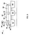
- FIG. 6illustrates a cross-sectional view 600 of the SRAM cell along the line 266 (shown in FIG. 2 ) in accordance with one embodiment of the present invention.
- one or more isolation regions 613are formed on the semiconductor substrate to define various device areas.
- a cap layer 602is formed on top of the poly gates 220 , while sidewall spacers 604 are formed on the edges of the poly gates 220 .
- An electrical interconnectionmust be made between metal 1 pad 302 , down through a via 606 and the silicide contact 212 , and to the gate poly 220 .
- the contact 212is formed at an opening in the cap layer 602 .
- the first portion of the gate poly 220 that lies inside the window 210must be electrically connected to the second portion that lies outside the window 210 .
- the first and second portionsare doped with different polarity types of impurities.
- An opening 612is opened in the cap layer 602 , thereby allowing a silicide contact 218 to form thereon.
- This silicide contact 218provides the necessary electrical connection between the first and second portions of the poly gate 220 .
- This contact 218does not receive any via, and therefore does not receive any electrical contact from metal 1 .
- the gate poly 220is electrically continuous from the low resistance of the contact 212 , through the relatively high resistance of its first portion, through the low resistance of the silicide contact 218 , and through the relatively high resistance of its second portion.
- This inventionprovides a method and structure for forming a silicide contact at the junction of two portions of the poly gate that are doped with different polarity types of impurities, thereby reducing the resistance therebetween. Furthermore, the invention provides an integrated method so that the silicide contacts at the junction and self-aligned contacts on source/drain regions can be realized in an integral semiconductor structure.
- a semiconductor substrate having a first device area and a second device areais provided.
- One or more isolation regionsare formed on the semiconductor substrate for defining the first and second device areas.
- a silicon gate layer across the first device area and the second device area on the semiconductor substrateare formed.
- a first portion of the silicon gate layer running across the first device areais doped with impurities of a first type, and a second portion of the silicon gate layer running across the second device area is doped with impurities of a second type.
- a cap layeris formed on the silicon gate layer for protecting the same covered thereunder from forming of a silicide structure, having at least one opening at a junction of the first and second portions of the silicon gate layer.
- a silicide layeris formed on the silicon gate layer that is exposed by the opening for reducing resistance at the junction between the first and second portions of the gate silicon layer.
- a first set of source/drain doped regionsare formed at two sides of the silicon gate layer in the first device area, and a second set of source/drain doped regions are formed at two sides of the silicon gate layer in the second device area.
- At least one self-aligned silicide contactis formed on the first and second sets of source/drain doped regions simultaneously in the step of forming the silicide layer.
Landscapes
- Engineering & Computer Science (AREA)
- Physics & Mathematics (AREA)
- Condensed Matter Physics & Semiconductors (AREA)
- General Physics & Mathematics (AREA)
- Manufacturing & Machinery (AREA)
- Computer Hardware Design (AREA)
- Microelectronics & Electronic Packaging (AREA)
- Power Engineering (AREA)
- Semiconductor Memories (AREA)
- Electrodes Of Semiconductors (AREA)
Abstract
Description
The present invention relates generally to integrated circuit (IC) designs, and more particularly to a semiconductor structure for reducing a gate resistance while providing a self-aligned silicide contact for a static random access memory (SRAM) cell.
As the semiconductor technology advances into the deep sub-micron realm, semiconductor structures become ever more crowded in an IC chip. SRAM cells, for instance, have become so dense that it has become increasingly difficult to form all the necessary electrical wiring in a SRAM chip. The interconnection structure from one metal interconnection wiring level to another, and also into the source/drain, gate, and body of a metal-oxide-semiconductor (MOS) transistor, require vertical conductive vias. In dual damascene metallization, metal, typically copper, is filled into etched vias and trenches, and excess is polished off by a process, such as chemical-mechanical-polish (CMP). Metal-filled vias provide vertical connections and metal-filled trenches provide lateral pads and lines.
Vias are typically the smallest features that must be resolved by lithography and etching. A metal-filled via down from the metal1 level to contacts on the active semiconductor substrate must be small enough to fit without causing an electrical short to any other substrate site, to a polycrystalline silicon (poly) line or gate, or to another via.
Two structures are often used to facilitate via formation down to a contact. The first is a silicide, a layer formed on top of a poly gate for providing an Ohm contact between the poly gate and via. The second is a self-aligned contact. Here, a cap layer is formed on the top surface of poly gates. In combination with spacers on the sidewalls of the poly gates, the cap layer fully insulates the poly gates on all sides. A metal layer is formed on source/drain regions of a semiconductor substrate. The semiconductor substrate is thermally treated to form silicide layers at the interfaces of the metal layer and the source/drain regions as self-aligned contacts. Due to the cap layer, the poly gate is protected from formation of silicide thereon during the thermal treatment process.
These two structures are rather mutually exclusive. If self-aligned contact is used, then the cap layer atop the poly gate prevents the formation of silicide on the poly gate. As a result, the poly gate is left with a resistance that is too high for proper circuit function.
Therefore, desirable in the art of integrated circuit designs are additional structures and methods for providing self-aligned silicide and self-aligned contacts in a simultaneous and effective fashion.
The present invention provides a semiconductor structure. In one embodiment, the semiconductor structure includes a semiconductor substrate having a first device area and a second device area. A gate layer is formed across the first device area and the second device area on the semiconductor substrate, wherein a first portion of the gate layer running across the first device area is doped with impurities of a first type, and a second portion of the gate layer running across the second device area is doped with impurities of a second type that is different from the first type. A cap layer is formed on the gate layer for protecting the same covered thereunder from forming a silicide structure, having at least one opening at a junction of the first and second portions of the gate layer. A silicide layer is formed on the gate layer that is exposed by the opening for reducing resistance at the junction between the first and second portions of the gate silicon layer.
The construction and method of operation of the invention, however, together with additional objects and advantages thereof will be best understood from the following description of specific embodiments when read in connection with the accompanying drawings.
The following will provide a detailed description of a structure for providing self-aligned silicide and self-aligned contacts in integral processes.
InFIG. 1 , a circuit diagram100 illustrates a standard SRAM cell having twocross-coupled inverters storage node 106 of theinverter 102 is connected to the gates of both transistors of theinverter 104. Astorage node 108 of theinverter 104 is connected to the gates of both transistors of theinverter 102. Thestorage node 106 of theinverter 102 is written to and read from by controlling atransfer transistor 110 that is coupled to a bit line BL. Thestorage node 108 of theinverter 104 is written to and read from by controlling atransfer transistor 112 that is coupled to a bit line bar BLB. Thetransfer transistors
InFIG. 2 , anIC layout 200 illustrates the construction of the SRAM cell up through readiness for metal1 deposition in accordance with one embodiment of the present invention. An SRAM cell is defined bylines contacts silicon gate 220 that controls a pull-up transistor118 (PU-2) and a pull-down transistor120 (PD-2), where part of a cap layer (identified bynumerals FIGS. 4 and 5 ) formed on the poly-silicon gate 220 has been removed. Thecontacts silicon gate 226 that controls a pull-up transistor114 (PU-1) and a pull-down transistor116 (PD-1), where part of a cap layer formed on the poly-silicon gate 226 has been removed. Inside awindow 210, which is a well of a second polarity type, first portions of thepoly gates window 210, which is another well of the first polarity type,poly gates poly gates
Referring toFIGS. 1 and 2 , thetransistor 114, which is a P-channel MOS transistor (also referred to as PMOS), has asource contact 232 that is connected to a power supply voltage VCC, and adrain contact 234 that is connected to thestorage node 106. Thetransistor 118, which is a PMOS transistor, has asource contact 236 that is connected to VCC, and adrain contact 238 that is connected to thestorage node 108. Thetransistor 116 is an NMOS transistor that has asource contact 240 connected to a complementary power supply voltage VSS, and adrain contact 242 that is connected to thestorage node 106. Thetransistors common poly gate 226. Thetransistor 120 is an NMOS transistor that has asource contact 244 connected to VSS, and adrain contact 246 that is connected to thestorage node 108. Thetransistors common poly gate 220.
A pass gate transistor110 (PG-1), which is an NMOS transistor, has asource contact 250 connected to a bit line BL (not shown in the figure), and thedrain contact 242 that is common to the drain contact of thetransistor 116 and connected to thestorage node 106. A pass gate transistor112 (PG-2), which is an NMOS transistor, has asource contact 254 that is connected to a bit line bar BLB (not shown in the figure), and thedrain contact 246 that is common to the drain contact of thetransistor 120 and connected to thestorage node 108.
Apoly gate 256 that controls thetransistor 110 has acontact 258 that is connected to a word line WL (not shown in the figure). A cap layer is formed on thepoly gate 256 outside thecontact 258, which will be explained further by paragraphs below with reference toFIGS. 4 and 5 . Apoly gate 260 that controls thetransistor 112 has acontact 262 that is connected to the word line WL (not shown in the figure). A cap layer is formed on thepoly gate 260 outside thecontact 262, which will also be explained further by paragraphs below with reference toFIGS. 4 and 5 . Across section line 264 runs through thetransistors cross section line 266 runs through thepoly gate 220. The cross-sectional views of the SRAM cell along thelines
InFIG. 3 , anIC layout 300 illustrates the construction of the SRAM cell up through metal1 deposition. With reference toFIGS. 1 through 3 , the SRAM cell is defined bylines pad 302 connecting thecontact 212 to thecontacts storage node 106, and an L-shapedpad 304 connecting thecontact 214 to thecontacts storage node 108. The landing pads comprise apad 306 connecting to thecontact 236, apad 308 connecting to thecontact 232, apad 310 connecting to thecontact 240, apad 312 connecting to thecontact 244, apad 314 connecting to thecontact 250, apad 316 connecting to thecontact 254, apad 318 connecting to thecontact 258, and apad 320 connecting to thecontact 262.
InFIG. 4 , across section 400 illustrates self-aligned silicide contacts formed on source/drain regions of MOS transistors in accordance with one embodiment of the present invention. Metal1402 is connected, byvias 404 to self-alignedsilicide contacts 406. Agate dielectric layer 408 is covered by apoly gate 410. Acap layer 412 is formed on thepoly gate 410.Sidewall spacers 414 are formed on the sidewalls of thepoly gates 410 and cap layers412. Since thepoly gates 410 are enclosed by the cap layers412 andspacers 414, they are protected from formation of silicide thereon during the formation of the self-alignedsilicide contacts 406 on source/drain regions 416. Furthermore, since thevias 404 are properly aligned, the via etch, a process required during the formation of thevias 404, causes no damage to any part of thepoly gates 410.
The cap layers412 includes a material of SiON, Ta2O5, A2O3, HfO, silicon oxide, silicon nitride, poly-ethyloxazoline (PEOX), tetra-ethylorthosilicate (TEOS), nitrogen-containing oxide, nitrided oxide, hafnium-containing oxide, tantalum-containing oxide, or aluminum-containing oxide. Thecap layer 412 includes one or more sub-layers made of different materials. For example, thecap layer 412 may include a first sub-layer made substantially of silicon oxide and a second sub-layer made substantially of silicon nitride. The self-alignedsilicide contacts 406 include a material of refractory metal, nitrided metal, Ti, TiSi2, Co, CoSi2, Ni, NiSi, TiN, TiW, or TaN. The gatedielectric layers 408 andspacers 414 include a material of SiON, Ta2O5, Al2O3, HfO, silicon oxide, silicon nitride, poly-ethyloxazoline (PEOX), tetra-ethylorthosilicate (TEOS), nitrogen-containing oxide, nitrided oxide, hafnium-containing oxide, tantalum-containing oxide, or aluminum-containing oxide.
InFIG. 5 , across section 500 illustrates self-aligned silicide contacts on source/drain regions of MOS transistors in accordance with one embodiment of the present invention. Metal1502 is connected, byvias 504 to self-alignedsilicide contacts 506. Agate dielectric layer 516 is covered by apoly gate 510. Acap layer 512 is formed on thepoly gate 510.Sidewall spacers 514 are formed on the sidewalls of thepoly gates 510 and cap layers512. Since theploy gates 510 are enclosed by the cap layers512 and thespacers 514, they are protected from formation of silicide thereon during the formation of thesilicide contacts 506. Furthermore, since thevias 504 are not properly aligned, the via etch causes damage to the cap layers512 andsidewall spacers 514. However, the etch damage is not significant. Sufficient amount of the cap layers506 and sidewall spacers508 protects thepoly gate 510 from significant etch damage.
This invention provides a method and structure for forming a silicide contact at the junction of two portions of the poly gate that are doped with different polarity types of impurities, thereby reducing the resistance therebetween. Furthermore, the invention provides an integrated method so that the silicide contacts at the junction and self-aligned contacts on source/drain regions can be realized in an integral semiconductor structure.
An exemplary method for forming the above proposed semiconductor structure is described as follows. A semiconductor substrate having a first device area and a second device area is provided. One or more isolation regions are formed on the semiconductor substrate for defining the first and second device areas. A silicon gate layer across the first device area and the second device area on the semiconductor substrate are formed. A first portion of the silicon gate layer running across the first device area is doped with impurities of a first type, and a second portion of the silicon gate layer running across the second device area is doped with impurities of a second type. A cap layer is formed on the silicon gate layer for protecting the same covered thereunder from forming of a silicide structure, having at least one opening at a junction of the first and second portions of the silicon gate layer. A silicide layer is formed on the silicon gate layer that is exposed by the opening for reducing resistance at the junction between the first and second portions of the gate silicon layer. A first set of source/drain doped regions are formed at two sides of the silicon gate layer in the first device area, and a second set of source/drain doped regions are formed at two sides of the silicon gate layer in the second device area. At least one self-aligned silicide contact is formed on the first and second sets of source/drain doped regions simultaneously in the step of forming the silicide layer.
The above illustration provides many different embodiments or embodiments for implementing different features of the invention. Specific embodiments of components and processes are described to help clarify the invention. These are, of course, merely embodiments and are not intended to limit the invention from that described in the claims.
Although the invention is illustrated and described herein as embodied in one or more specific examples, it is nevertheless not intended to be limited to the details shown, since various modifications and structural changes may be made therein without departing from the spirit of the invention and within the scope and range of equivalents of the claims. Accordingly, it is appropriate that the appended claims be construed broadly and in a manner consistent with the scope of the invention, as set forth in the following claims.
Claims (14)
1. A semiconductor structure comprising:
a semiconductor substrate having a first device area and a second device area;
a gate layer formed across the first device area and the second device area on the semiconductor substrate, wherein a first portion of the gate layer running across the first device area is doped with impurities of a first type, and a second portion of the gate layer running across the second device area is doped with impurities of a second type;
one or more source/drain doped regions at two sides of the gate layer;
one or more spacers formed on sidewalls of the gate layer;
a cap layer formed on the gate layer for protecting the same that is covered thereunder from forming a silicide structure, the cap layer having a first opening at a junction of the first and second portions of the gate layer and a second opening at another portion of the gate layer for interconnections between the gate layer and an overlying conductive layer;
one or more vias formed on the source/drain doped regions; and
a silicide layer formed on the source/drain doped regions and on the gate layer that is exposed by the first opening and the second opening, wherein the overlying conductive layer is connected to the silicide layer formed on the source/drain doped regions and the gate layer exposed by the second opening.
2. The semiconductor structure ofclaim 1 wherein the cap layer further comprises one or more sub-layers made of different materials.
3. The semiconductor structure ofclaim 2 wherein the cap layer further comprises a first sub-layer made substantially of silicon oxide and a second sub-layer made substantially of silicon nitride.
4. The semiconductor structure ofclaim 1 wherein the cap layer includes a material of SiON, Ta2O5, Al2O3, HfO, silicon oxide, silicon nitride, poly-ethyloxazoline (PEOX), tetra-ethylorthosilicate (TEOS), nitrogen-containing oxide, nitrided oxide, hafnium-containing oxide, tantalum-containing oxide, aluminum-containing oxide, or high K dielectric materials with a dielectric constant K larger than 5.
5. The semiconductor structure ofclaim 1 further comprising one or more isolation regions formed on the semiconductor substrate, defining the first and second device areas.
6. The semiconductor structure ofclaim 5 further comprising a first set of source/drain doped regions at two sides of the gate layer in the first device area and a second set of source/drain doped regions at two sides of the gate layer in the second device area.
7. The semiconductor structure ofclaim 6 further comprising at least one self-aligned silicide contact formed on the first and second sets of source/drain doped regions.
8. The semiconductor structure ofclaim 7 further comprising a gate dielectric layer formed between the gate layer and the semiconductor substrate for separating one from another.
9. The semiconductor structure ofclaim 8 further comprising one or more spacers formed on sidewalls of the silicon gate layer and cap layers.
10. The semiconductor structure ofclaim 1 wherein the silicide layer includes a material of refractory metal, nitrided metal, Ti, TiSi2, Co, CoSi2, Ni, NiSi, TiN, TiW, or TaN.
11. A semiconductor structure for serving as an inverter in a static random access memory (SRAM) cell, comprising:
a semiconductor substrate having a first device area and a second device area;
a gate layer formed across the first device area and the second device area on the semiconductor substrate, wherein a first portion of the gate layer running across the first device area is doped with impurities of a first type, and a second portion of the gate layer running across the second device area is doped with impurities of a second type;
a gate dielectric layer formed between the gate layer and the semiconductor substrate for separating one from another;
a first set of source/drain doped regions at two sides of the gate layer in the first device area;
a second set of source/drain doped regions at two sides of the gate layer in the second device area;
one or more spacers formed on sidewalls of the gate layer;
a cap layer formed on the gate layer for protecting the same covered thereunder from forming a silicide structure, having a first opening at a junction of the first and second portions of the gate layer and a second opening at another portion of the gate layer for interconnections between the gate layer and an overlying conductive layer;
one or more vias formed on the first set and second set of source/drain doped regions;
a silicide layer formed on the gate layer that is exposed by the first opening and the second opening for reducing resistance at the junction between the first and second portions of the gate silicon layer; and
at least one self-aligned silicide contact formed on one of the first and second source/drain doped regions, wherein the overlying conductive layer is connected to the self-aligned silicide contact and the gate layer exposed by the second opening.
12. The semiconductor structure ofclaim 11 wherein the cap layer further comprises a first sub-layer made of a first material and a second sub-layer made of a second material different from the first material.
13. The semiconductor structure ofclaim 11 wherein the cap layer includes a material of SiON, Ta2O5, Al2O3, HfO, silicon oxide, silicon nitride, poly-ethyloxazoline (PEOX), tetra-ethylorthosilicate (TEOS), nitrogen-containing oxide, nitrided oxide, hafnium-containing oxide, tantalum-containing oxide, or aluminum-containing oxide.
14. The semiconductor structure ofclaim 11 wherein the silicide layer includes a material of refractory metal, nitrided metal, Ti, TiSi2, Co, CoSi2, Ni, NiSi, TiN, TiW, or TaN.
Priority Applications (3)
| Application Number | Priority Date | Filing Date | Title |
|---|---|---|---|
| US11/257,572US7485934B2 (en) | 2005-10-25 | 2005-10-25 | Integrated semiconductor structure for SRAM cells |
| TW095109587ATWI321829B (en) | 2005-10-25 | 2006-03-21 | Semiconductor structure and method for forming the semiconductor structure |
| CNB2006100735022ACN100470833C (en) | 2005-10-25 | 2006-04-12 | Semiconductor structure and forming method thereof |
Applications Claiming Priority (1)
| Application Number | Priority Date | Filing Date | Title |
|---|---|---|---|
| US11/257,572US7485934B2 (en) | 2005-10-25 | 2005-10-25 | Integrated semiconductor structure for SRAM cells |
Publications (2)
| Publication Number | Publication Date |
|---|---|
| US20070090428A1 US20070090428A1 (en) | 2007-04-26 |
| US7485934B2true US7485934B2 (en) | 2009-02-03 |
Family
ID=37984536
Family Applications (1)
| Application Number | Title | Priority Date | Filing Date |
|---|---|---|---|
| US11/257,572Active2026-08-04US7485934B2 (en) | 2005-10-25 | 2005-10-25 | Integrated semiconductor structure for SRAM cells |
Country Status (3)
| Country | Link |
|---|---|
| US (1) | US7485934B2 (en) |
| CN (1) | CN100470833C (en) |
| TW (1) | TWI321829B (en) |
Cited By (25)
| Publication number | Priority date | Publication date | Assignee | Title |
|---|---|---|---|---|
| US20080157221A1 (en)* | 2006-12-27 | 2008-07-03 | Yong-Geun Lee | Structure of semiconductor device for decreasing chip area and manufacturing method thereof |
| US20080222587A1 (en)* | 2007-03-05 | 2008-09-11 | Tela Innovations, Inc. | Integrated Circuit Cell Library for Multiple Patterning |
| US20100187616A1 (en)* | 2008-03-13 | 2010-07-29 | Tela Innovations, Inc. | Linear Gate Level Cross-Coupled Transistor Device with Overlapping PMOS Transistors and Overlapping NMOS Transistors Relative to Direction of Gate Electrodes |
| US20110161909A1 (en)* | 2007-08-02 | 2011-06-30 | Tela Innovations, Inc. | Methods for Designing Semiconductor Device with Dynamic Array Section |
| US8436405B2 (en) | 2010-06-30 | 2013-05-07 | Taiwan Semiconductor Manufacturing Company, Ltd. | ROM cell circuit for FinFET devices |
| US20130242645A1 (en)* | 2010-07-20 | 2013-09-19 | University Of Virginia Patent Foundation | Memory Cell |
| US8541879B2 (en) | 2007-12-13 | 2013-09-24 | Tela Innovations, Inc. | Super-self-aligned contacts and method for making the same |
| US8549455B2 (en) | 2007-08-02 | 2013-10-01 | Tela Innovations, Inc. | Methods for cell phasing and placement in dynamic array architecture and implementation of the same |
| US8653857B2 (en) | 2006-03-09 | 2014-02-18 | Tela Innovations, Inc. | Circuitry and layouts for XOR and XNOR logic |
| US8658542B2 (en) | 2006-03-09 | 2014-02-25 | Tela Innovations, Inc. | Coarse grid design methods and structures |
| US8661392B2 (en) | 2009-10-13 | 2014-02-25 | Tela Innovations, Inc. | Methods for cell boundary encroachment and layouts implementing the Same |
| US8680626B2 (en) | 2007-10-26 | 2014-03-25 | Tela Innovations, Inc. | Methods, structures, and designs for self-aligning local interconnects used in integrated circuits |
| US8701071B2 (en) | 2008-01-31 | 2014-04-15 | Tela Innovations, Inc. | Enforcement of semiconductor structure regularity for localized transistors and interconnect |
| US8759985B2 (en) | 2008-03-27 | 2014-06-24 | Tela Innovations, Inc. | Methods for multi-wire routing and apparatus implementing same |
| US8823062B2 (en) | 2006-03-09 | 2014-09-02 | Tela Innovations, Inc. | Integrated circuit with offset line end spacings in linear gate electrode level |
| US8839175B2 (en) | 2006-03-09 | 2014-09-16 | Tela Innovations, Inc. | Scalable meta-data objects |
| US8863063B2 (en) | 2009-05-06 | 2014-10-14 | Tela Innovations, Inc. | Finfet transistor circuit |
| US9035359B2 (en) | 2006-03-09 | 2015-05-19 | Tela Innovations, Inc. | Semiconductor chip including region including linear-shaped conductive structures forming gate electrodes and having electrical connection areas arranged relative to inner region between transistors of different types and associated methods |
| US9122832B2 (en) | 2008-08-01 | 2015-09-01 | Tela Innovations, Inc. | Methods for controlling microloading variation in semiconductor wafer layout and fabrication |
| US9159627B2 (en) | 2010-11-12 | 2015-10-13 | Tela Innovations, Inc. | Methods for linewidth modification and apparatus implementing the same |
| US9230910B2 (en) | 2006-03-09 | 2016-01-05 | Tela Innovations, Inc. | Oversized contacts and vias in layout defined by linearly constrained topology |
| US9563733B2 (en) | 2009-05-06 | 2017-02-07 | Tela Innovations, Inc. | Cell circuit and layout with linear finfet structures |
| US9754878B2 (en) | 2006-03-09 | 2017-09-05 | Tela Innovations, Inc. | Semiconductor chip including a chip level based on a layout that includes both regular and irregular wires |
| USRE47207E1 (en) | 2010-06-25 | 2019-01-15 | Taiwan Semiconductor Manufacturing Company, Ltd. | Cell structure for dual-port SRAM |
| USRE47409E1 (en) | 2010-06-30 | 2019-05-28 | Taiwan Semiconductor Manufacturing Company, Ltd. | Layout for multiple-fin SRAM cell |
Families Citing this family (8)
| Publication number | Priority date | Publication date | Assignee | Title |
|---|---|---|---|---|
| US7869262B2 (en)* | 2007-01-29 | 2011-01-11 | Taiwan Semiconductor Manufacturing Co., Ltd. | Memory device with an asymmetric layout structure |
| US8188550B2 (en)* | 2007-12-27 | 2012-05-29 | Globalfoundries Singapore Pte. Ltd. | Integrated circuit structure with electrical strap and its method of forming |
| US8942030B2 (en) | 2010-06-25 | 2015-01-27 | Taiwan Semiconductor Manufacturing Company, Ltd. | Structure and method for SRAM cell circuit |
| US8315084B2 (en)* | 2010-03-10 | 2012-11-20 | Taiwan Semiconductor Manufacturing Company, Ltd. | Fully balanced dual-port memory cell |
| US8735972B2 (en)* | 2011-09-08 | 2014-05-27 | International Business Machines Corporation | SRAM cell having recessed storage node connections and method of fabricating same |
| US9911727B2 (en) | 2015-03-16 | 2018-03-06 | Taiwan Semiconductor Manufacturing Company, Ltd. | Strapping structure of memory circuit |
| DE102016118207B4 (en)* | 2015-12-30 | 2024-08-01 | Taiwan Semiconductor Manufacturing Co. Ltd. | SEMICONDUCTOR DEVICE AND METHOD FOR MANUFACTURING THE SAME |
| US10804148B2 (en)* | 2017-08-25 | 2020-10-13 | International Business Machines Corporation | Buried contact to provide reduced VFET feature-to-feature tolerance requirements |
Citations (5)
| Publication number | Priority date | Publication date | Assignee | Title |
|---|---|---|---|---|
| US6198143B1 (en)* | 1989-07-14 | 2001-03-06 | Mitsubishi Denki Kabushiki Kaisha | Semiconductor device including a layer of thermally stable titanium silicide |
| US20020028569A1 (en)* | 1999-08-02 | 2002-03-07 | Mitsubishi Denki Kabushiki Kaisha | Semiconductor device and method of manufacturing same |
| US6583518B2 (en)* | 2001-08-31 | 2003-06-24 | Micron Technology, Inc. | Cross-diffusion resistant dual-polycide semiconductor structure and method |
| US6700163B2 (en)* | 2001-12-07 | 2004-03-02 | International Business Machines Corporation | Selective silicide blocking |
| US6841429B2 (en)* | 2002-08-12 | 2005-01-11 | Kabushiki Kaisha Toshiba | Method of manufacturing a semiconductor device having a silicide film |
Family Cites Families (2)
| Publication number | Priority date | Publication date | Assignee | Title |
|---|---|---|---|---|
| CN1055785C (en)* | 1996-12-10 | 2000-08-23 | 联华电子股份有限公司 | Self-aligned silicide manufacturing method |
| JP2980057B2 (en)* | 1997-04-30 | 1999-11-22 | 日本電気株式会社 | Method for manufacturing semiconductor device |
- 2005
- 2005-10-25USUS11/257,572patent/US7485934B2/enactiveActive
- 2006
- 2006-03-21TWTW095109587Apatent/TWI321829B/enactive
- 2006-04-12CNCNB2006100735022Apatent/CN100470833C/enactiveActive
Patent Citations (5)
| Publication number | Priority date | Publication date | Assignee | Title |
|---|---|---|---|---|
| US6198143B1 (en)* | 1989-07-14 | 2001-03-06 | Mitsubishi Denki Kabushiki Kaisha | Semiconductor device including a layer of thermally stable titanium silicide |
| US20020028569A1 (en)* | 1999-08-02 | 2002-03-07 | Mitsubishi Denki Kabushiki Kaisha | Semiconductor device and method of manufacturing same |
| US6583518B2 (en)* | 2001-08-31 | 2003-06-24 | Micron Technology, Inc. | Cross-diffusion resistant dual-polycide semiconductor structure and method |
| US6700163B2 (en)* | 2001-12-07 | 2004-03-02 | International Business Machines Corporation | Selective silicide blocking |
| US6841429B2 (en)* | 2002-08-12 | 2005-01-11 | Kabushiki Kaisha Toshiba | Method of manufacturing a semiconductor device having a silicide film |
Cited By (121)
| Publication number | Priority date | Publication date | Assignee | Title |
|---|---|---|---|---|
| US9230910B2 (en) | 2006-03-09 | 2016-01-05 | Tela Innovations, Inc. | Oversized contacts and vias in layout defined by linearly constrained topology |
| US9589091B2 (en) | 2006-03-09 | 2017-03-07 | Tela Innovations, Inc. | Scalable meta-data objects |
| US10230377B2 (en) | 2006-03-09 | 2019-03-12 | Tela Innovations, Inc. | Circuitry and layouts for XOR and XNOR logic |
| US10217763B2 (en) | 2006-03-09 | 2019-02-26 | Tela Innovations, Inc. | Semiconductor chip having region including gate electrode features of rectangular shape on gate horizontal grid and first-metal structures of rectangular shape on at least eight first-metal gridlines of first-metal vertical grid |
| US10186523B2 (en) | 2006-03-09 | 2019-01-22 | Tela Innovations, Inc. | Semiconductor chip having region including gate electrode features formed in part from rectangular layout shapes on gate horizontal grid and first-metal structures formed in part from rectangular layout shapes on at least eight first-metal gridlines of first-metal vertical grid |
| US10141334B2 (en) | 2006-03-09 | 2018-11-27 | Tela Innovations, Inc. | Semiconductor chip including region having rectangular-shaped gate structures and first-metal structures |
| US10141335B2 (en) | 2006-03-09 | 2018-11-27 | Tela Innovations, Inc. | Semiconductor CIP including region having rectangular-shaped gate structures and first metal structures |
| US8839175B2 (en) | 2006-03-09 | 2014-09-16 | Tela Innovations, Inc. | Scalable meta-data objects |
| US9917056B2 (en) | 2006-03-09 | 2018-03-13 | Tela Innovations, Inc. | Coarse grid design methods and structures |
| US9905576B2 (en) | 2006-03-09 | 2018-02-27 | Tela Innovations, Inc. | Semiconductor chip including region having rectangular-shaped gate structures and first metal structures |
| US9859277B2 (en) | 2006-03-09 | 2018-01-02 | Tela Innovations, Inc. | Methods, structures, and designs for self-aligning local interconnects used in integrated circuits |
| US9754878B2 (en) | 2006-03-09 | 2017-09-05 | Tela Innovations, Inc. | Semiconductor chip including a chip level based on a layout that includes both regular and irregular wires |
| US9741719B2 (en) | 2006-03-09 | 2017-08-22 | Tela Innovations, Inc. | Methods, structures, and designs for self-aligning local interconnects used in integrated circuits |
| US9711495B2 (en) | 2006-03-09 | 2017-07-18 | Tela Innovations, Inc. | Oversized contacts and vias in layout defined by linearly constrained topology |
| US9673825B2 (en) | 2006-03-09 | 2017-06-06 | Tela Innovations, Inc. | Circuitry and layouts for XOR and XNOR logic |
| US8921897B2 (en) | 2006-03-09 | 2014-12-30 | Tela Innovations, Inc. | Integrated circuit with gate electrode conductive structures having offset ends |
| US8921896B2 (en) | 2006-03-09 | 2014-12-30 | Tela Innovations, Inc. | Integrated circuit including linear gate electrode structures having different extension distances beyond contact |
| US8946781B2 (en) | 2006-03-09 | 2015-02-03 | Tela Innovations, Inc. | Integrated circuit including gate electrode conductive structures with different extension distances beyond contact |
| US9443947B2 (en) | 2006-03-09 | 2016-09-13 | Tela Innovations, Inc. | Semiconductor chip including region having integrated circuit transistor gate electrodes formed by various conductive structures of specified shape and position and method for manufacturing the same |
| US9425273B2 (en) | 2006-03-09 | 2016-08-23 | Tela Innovations, Inc. | Semiconductor chip including integrated circuit including at least five gate level conductive structures having particular spatial and electrical relationship and method for manufacturing the same |
| US9425145B2 (en) | 2006-03-09 | 2016-08-23 | Tela Innovations, Inc. | Oversized contacts and vias in layout defined by linearly constrained topology |
| US9425272B2 (en) | 2006-03-09 | 2016-08-23 | Tela Innovations, Inc. | Semiconductor chip including integrated circuit including four transistors of first transistor type and four transistors of second transistor type with electrical connections between various transistors and methods for manufacturing the same |
| US9336344B2 (en) | 2006-03-09 | 2016-05-10 | Tela Innovations, Inc. | Coarse grid design methods and structures |
| US9240413B2 (en) | 2006-03-09 | 2016-01-19 | Tela Innovations, Inc. | Methods, structures, and designs for self-aligning local interconnects used in integrated circuits |
| US8823062B2 (en) | 2006-03-09 | 2014-09-02 | Tela Innovations, Inc. | Integrated circuit with offset line end spacings in linear gate electrode level |
| US8653857B2 (en) | 2006-03-09 | 2014-02-18 | Tela Innovations, Inc. | Circuitry and layouts for XOR and XNOR logic |
| US8658542B2 (en) | 2006-03-09 | 2014-02-25 | Tela Innovations, Inc. | Coarse grid design methods and structures |
| US9035359B2 (en) | 2006-03-09 | 2015-05-19 | Tela Innovations, Inc. | Semiconductor chip including region including linear-shaped conductive structures forming gate electrodes and having electrical connection areas arranged relative to inner region between transistors of different types and associated methods |
| US8952425B2 (en) | 2006-03-09 | 2015-02-10 | Tela Innovations, Inc. | Integrated circuit including at least four linear-shaped conductive structures having extending portions of different length |
| US9009641B2 (en) | 2006-03-09 | 2015-04-14 | Tela Innovations, Inc. | Circuits with linear finfet structures |
| US20080157221A1 (en)* | 2006-12-27 | 2008-07-03 | Yong-Geun Lee | Structure of semiconductor device for decreasing chip area and manufacturing method thereof |
| US8667443B2 (en) | 2007-03-05 | 2014-03-04 | Tela Innovations, Inc. | Integrated circuit cell library for multiple patterning |
| US20080222587A1 (en)* | 2007-03-05 | 2008-09-11 | Tela Innovations, Inc. | Integrated Circuit Cell Library for Multiple Patterning |
| US9633987B2 (en) | 2007-03-05 | 2017-04-25 | Tela Innovations, Inc. | Integrated circuit cell library for multiple patterning |
| US10074640B2 (en) | 2007-03-05 | 2018-09-11 | Tela Innovations, Inc. | Integrated circuit cell library for multiple patterning |
| US9595515B2 (en) | 2007-03-07 | 2017-03-14 | Tela Innovations, Inc. | Semiconductor chip including integrated circuit defined within dynamic array section |
| US9910950B2 (en) | 2007-03-07 | 2018-03-06 | Tela Innovations, Inc. | Methods for cell phasing and placement in dynamic array architecture and implementation of the same |
| US8966424B2 (en) | 2007-03-07 | 2015-02-24 | Tela Innovations, Inc. | Methods for cell phasing and placement in dynamic array architecture and implementation of the same |
| US9424387B2 (en) | 2007-03-07 | 2016-08-23 | Tela Innovations, Inc. | Methods for cell phasing and placement in dynamic array architecture and implementation of the same |
| US8549455B2 (en) | 2007-08-02 | 2013-10-01 | Tela Innovations, Inc. | Methods for cell phasing and placement in dynamic array architecture and implementation of the same |
| US8756551B2 (en) | 2007-08-02 | 2014-06-17 | Tela Innovations, Inc. | Methods for designing semiconductor device with dynamic array section |
| US20110161909A1 (en)* | 2007-08-02 | 2011-06-30 | Tela Innovations, Inc. | Methods for Designing Semiconductor Device with Dynamic Array Section |
| US8759882B2 (en) | 2007-08-02 | 2014-06-24 | Tela Innovations, Inc. | Semiconductor device with dynamic array sections defined and placed according to manufacturing assurance halos |
| US10734383B2 (en) | 2007-10-26 | 2020-08-04 | Tela Innovations, Inc. | Methods, structures, and designs for self-aligning local interconnects used in integrated circuits |
| US8680626B2 (en) | 2007-10-26 | 2014-03-25 | Tela Innovations, Inc. | Methods, structures, and designs for self-aligning local interconnects used in integrated circuits |
| US8541879B2 (en) | 2007-12-13 | 2013-09-24 | Tela Innovations, Inc. | Super-self-aligned contacts and method for making the same |
| US9281371B2 (en) | 2007-12-13 | 2016-03-08 | Tela Innovations, Inc. | Super-self-aligned contacts and method for making the same |
| US9818747B2 (en) | 2007-12-13 | 2017-11-14 | Tela Innovations, Inc. | Super-self-aligned contacts and method for making the same |
| US8951916B2 (en) | 2007-12-13 | 2015-02-10 | Tela Innovations, Inc. | Super-self-aligned contacts and method for making the same |
| US10461081B2 (en) | 2007-12-13 | 2019-10-29 | Tel Innovations, Inc. | Super-self-aligned contacts and method for making the same |
| US9530734B2 (en) | 2008-01-31 | 2016-12-27 | Tela Innovations, Inc. | Enforcement of semiconductor structure regularity for localized transistors and interconnect |
| US8701071B2 (en) | 2008-01-31 | 2014-04-15 | Tela Innovations, Inc. | Enforcement of semiconductor structure regularity for localized transistors and interconnect |
| US9202779B2 (en) | 2008-01-31 | 2015-12-01 | Tela Innovations, Inc. | Enforcement of semiconductor structure regularity for localized transistors and interconnect |
| US8866197B2 (en) | 2008-03-13 | 2014-10-21 | Tela Innovations, Inc. | Integrated circuit including cross-coupled transistors having gate electrodes formed within gate level feature layout channels with at least two gate electrodes electrically connected to each other through another transistor forming gate level feature |
| US20100258879A1 (en)* | 2008-03-13 | 2010-10-14 | Tela Innovations, Inc. | Channelized Gate Level Cross-Coupled Transistor Device with Cross-Coupled Transistor Gate Electrode Connections Made Using Linear First Interconnect Level above Gate Electrode Level |
| US8735995B2 (en) | 2008-03-13 | 2014-05-27 | Tela Innovations, Inc. | Cross-coupled transistor circuit defined on three gate electrode tracks with diffusion regions of common node on opposing sides of same gate electrode track |
| US8735944B2 (en) | 2008-03-13 | 2014-05-27 | Tela Innovations, Inc. | Integrated circuit including cross-coupled transistors having gate electrodes formed within gate level feature layout channels with serially connected transistors |
| US8872283B2 (en) | 2008-03-13 | 2014-10-28 | Tela Innovations, Inc. | Integrated circuit including cross-coupled transistors having gate electrodes formed within gate level feature layout channels with shared diffusion regions on opposite sides of two-transistor-forming gate level feature |
| US8853794B2 (en) | 2008-03-13 | 2014-10-07 | Tela Innovations, Inc. | Integrated circuit within semiconductor chip including cross-coupled transistor configuration |
| US8680583B2 (en) | 2008-03-13 | 2014-03-25 | Tela Innovations, Inc. | Integrated circuit including cross-coupled transistors having gate electrodes formed within at least nine gate level feature layout channels |
| US8847331B2 (en) | 2008-03-13 | 2014-09-30 | Tela Innovations, Inc. | Semiconductor chip including region having cross-coupled transistor configuration with offset electrical connection areas on gate electrode forming conductive structures and at least two different inner extension distances of gate electrode forming conductive structures |
| US10727252B2 (en) | 2008-03-13 | 2020-07-28 | Tela Innovations, Inc. | Semiconductor chip including integrated circuit having cross-coupled transistor configuration and method for manufacturing the same |
| US8847329B2 (en) | 2008-03-13 | 2014-09-30 | Tela Innovations, Inc. | Cross-coupled transistor circuit defined having diffusion regions of common node on opposing sides of same gate electrode track with at least two non-inner positioned gate contacts |
| US8669594B2 (en) | 2008-03-13 | 2014-03-11 | Tela Innovations, Inc. | Integrated circuit including cross-coupled transistors having gate electrodes formed within at least twelve gate level feature layout channels |
| US8729606B2 (en) | 2008-03-13 | 2014-05-20 | Tela Innovations, Inc. | Integrated circuit including cross-coupled transistors having gate electrodes formed within gate level feature layout channels |
| US8669595B2 (en) | 2008-03-13 | 2014-03-11 | Tela Innovations, Inc. | Integrated circuit including cross-coupled transistors having gate electrodes formed within gate level feature layout channels with gate contact position, alignment, and offset specifications |
| US10658385B2 (en) | 2008-03-13 | 2020-05-19 | Tela Innovations, Inc. | Cross-coupled transistor circuit defined on four gate electrode tracks |
| US9081931B2 (en) | 2008-03-13 | 2015-07-14 | Tela Innovations, Inc. | Cross-coupled transistor circuit having diffusion regions of common node on opposing sides of same gate electrode track and gate node connection through single interconnect layer |
| US9117050B2 (en) | 2008-03-13 | 2015-08-25 | Tela Innovations, Inc. | Integrated circuit including cross-coupled transistors having gate electrodes formed within gate level feature layout channels with gate contact position and offset specifications |
| US10651200B2 (en) | 2008-03-13 | 2020-05-12 | Tela Innovations, Inc. | Cross-coupled transistor circuit defined on three gate electrode tracks |
| US8742463B2 (en) | 2008-03-13 | 2014-06-03 | Tela Innovations, Inc. | Integrated circuit including cross-coupled transistors having gate electrodes formed within gate level feature layout channels with outer positioned gate contacts |
| US8835989B2 (en) | 2008-03-13 | 2014-09-16 | Tela Innovations, Inc. | Integrated circuit including cross-coupled transistors having gate electrodes formed within gate level feature layout channels with gate electrode placement specifications |
| US9208279B2 (en) | 2008-03-13 | 2015-12-08 | Tela Innovations, Inc. | Semiconductor chip including digital logic circuit including linear-shaped conductive structures having electrical connection areas located within inner region between transistors of different type and associated methods |
| US9213792B2 (en) | 2008-03-13 | 2015-12-15 | Tela Innovations, Inc. | Semiconductor chip including digital logic circuit including at least six transistors with some transistors forming cross-coupled transistor configuration and associated methods |
| US8592872B2 (en) | 2008-03-13 | 2013-11-26 | Tela Innovations, Inc. | Integrated circuit including cross-coupled transistors with two transistors of different type having gate electrodes formed by common gate level feature with shared diffusion regions on opposite sides of common gate level feature |
| US8587034B2 (en) | 2008-03-13 | 2013-11-19 | Tela Innovations, Inc. | Integrated circuit including cross-coupled transistors having gate electrodes formed within gate level feature layout channels with four inside positioned gate contacts and electrical connection of transistor gates through linear interconnect conductors in single interconnect layer |
| US9245081B2 (en) | 2008-03-13 | 2016-01-26 | Tela Innovations, Inc. | Semiconductor chip including digital logic circuit including at least nine linear-shaped conductive structures collectively forming gate electrodes of at least six transistors with some transistors forming cross-coupled transistor configuration and associated methods |
| US20100187616A1 (en)* | 2008-03-13 | 2010-07-29 | Tela Innovations, Inc. | Linear Gate Level Cross-Coupled Transistor Device with Overlapping PMOS Transistors and Overlapping NMOS Transistors Relative to Direction of Gate Electrodes |
| US8836045B2 (en) | 2008-03-13 | 2014-09-16 | Tela Innovations, Inc. | Cross-coupled transistor circuit having diffusion regions of common node on opposing sides of same gate electrode track |
| US8581304B2 (en) | 2008-03-13 | 2013-11-12 | Tela Innovations, Inc. | Integrated circuit including cross-coupled transistors having gate electrodes formed within gate level feature layout channels with four inside positioned gate contacts having offset and aligned relationships |
| US20100187627A1 (en)* | 2008-03-13 | 2010-07-29 | Tela Innovations, Inc. | Channelized Gate Level Cross-Coupled Transistor Device with Overlapping PMOS Transistors and Overlapping NMOS Transistors Relative to Direction of Gate Electrodes |
| US8581303B2 (en) | 2008-03-13 | 2013-11-12 | Tela Innovations, Inc. | Integrated circuit including cross-coupled trasistors having gate electrodes formed within gate level feature layout channels with four inside positioned gate contacts having offset relationships and electrical connection of cross-coupled transistors through same interconnect layer |
| US8575706B2 (en) | 2008-03-13 | 2013-11-05 | Tela Innovations, Inc. | Integrated circuit including cross-coupled transistors having gate electrodes formed within gate level feature layout channels with at least two different gate level features inner extensions beyond gate electrode |
| US8569841B2 (en) | 2008-03-13 | 2013-10-29 | Tela Innovations, Inc. | Integrated circuit including cross-coupled transistors having gate electrodes formed within gate level feature layout channels with at least one gate level feature extending into adjacent gate level feature layout channel |
| US8729643B2 (en) | 2008-03-13 | 2014-05-20 | Tela Innovations, Inc. | Cross-coupled transistor circuit including offset inner gate contacts |
| US8564071B2 (en) | 2008-03-13 | 2013-10-22 | Tela Innovations, Inc. | Integrated circuit including cross-coupled transistors having gate electrodes formed within gate level feature layout channels with at least two different gate level feature extensions beyond contact |
| US8816402B2 (en) | 2008-03-13 | 2014-08-26 | Tela Innovations, Inc. | Integrated circuit including cross-coupled transistors having gate electrodes formed within gate level feature layout channels with gate level feature layout channel including single transistor |
| US20100187634A1 (en)* | 2008-03-13 | 2010-07-29 | Tela Innovations, Inc. | Channelized Gate Level Cross-Coupled Transistor Device with Cross-Coupled Transistors Defined on Four Gate Electrode Tracks with Crossing Gate Electrode Connections |
| US9536899B2 (en) | 2008-03-13 | 2017-01-03 | Tela Innovations, Inc. | Semiconductor chip including integrated circuit having cross-coupled transistor configuration and method for manufacturing the same |
| US20100187621A1 (en)* | 2008-03-13 | 2010-07-29 | Tela Innovations, Inc. | Linear Gate Level Cross-Coupled Transistor Device with Constant Gate Electrode Pitch |
| US8558322B2 (en) | 2008-03-13 | 2013-10-15 | Tela Innovations, Inc. | Integrated circuit including cross-coupled transistors having gate electrodes formed within gate level feature layout channels with at least two gate electrodes electrically connected to each other through gate level feature |
| US8552508B2 (en) | 2008-03-13 | 2013-10-08 | Tela Innovations, Inc. | Integrated circuit including cross-coupled transistors having gate electrodes formed within gate level feature layout channels with shared diffusion regions on opposite sides of two-transistor-forming gate level feature and electrical connection of transistor gates through linear interconnect conductors in single interconnect layer |
| US8552509B2 (en) | 2008-03-13 | 2013-10-08 | Tela Innovations, Inc. | Integrated circuit including cross-coupled transistors having gate electrodes formed within gate level feature layout channels with other transistors positioned between cross-coupled transistors |
| US8785978B2 (en) | 2008-03-13 | 2014-07-22 | Tela Innovations, Inc. | Integrated circuit including cross-coupled transistors having gate electrodes formed within gate level feature layout channels with electrical connection of cross-coupled transistors through same interconnect layer |
| US20100237429A1 (en)* | 2008-03-13 | 2010-09-23 | Tela Innovations, Inc. | Channelized Gate Level Cross-Coupled Transistor Device with Non-Overlapping PMOS Transistors and Non-Overlapping NMOS Transistors Relative to Direction of Gate Electrodes |
| US8785979B2 (en) | 2008-03-13 | 2014-07-22 | Tela Innovations, Inc. | Integrated circuit including cross-coupled transistors having gate electrodes formed within gate level feature layout channels with two inside positioned gate contacts and two outside positioned gate contacts and electrical connection of cross-coupled transistors through same interconnect layer |
| US20100237427A1 (en)* | 2008-03-13 | 2010-09-23 | Tela Innovations, Inc. | Channelized Gate Level Cross-Coupled Transistor Device with Contiguous p-type Diffusion Regions and Contiguous n-type Diffusion Regions |
| US10020321B2 (en) | 2008-03-13 | 2018-07-10 | Tela Innovations, Inc. | Cross-coupled transistor circuit defined on two gate electrode tracks |
| US20100252893A1 (en)* | 2008-03-13 | 2010-10-07 | Tela Innovations, Inc. | Channelized Gate Level Cross-Coupled Transistor Device with Cross-Coupled Transistors Defined on Three Gate Electrode Tracks with Crossing Gate Electrode Connections |
| US8772839B2 (en) | 2008-03-13 | 2014-07-08 | Tela Innovations, Inc. | Integrated circuit including cross-coupled transistors having gate electrodes formed within gate level feature layout channels with four inside positioned gate contacts having offset and aligned relationships and electrical connection of transistor gates through linear interconnect conductors in single interconnect layer |
| US8742462B2 (en) | 2008-03-13 | 2014-06-03 | Tela Innovations, Inc. | Integrated circuit including cross-coupled transistors having gate electrodes formed within gate level feature layout channels with gate contact position specifications |
| US9871056B2 (en) | 2008-03-13 | 2018-01-16 | Tela Innovations, Inc. | Semiconductor chip including integrated circuit having cross-coupled transistor configuration and method for manufacturing the same |
| US8853793B2 (en) | 2008-03-13 | 2014-10-07 | Tela Innovations, Inc. | Integrated circuit including gate electrode level region including cross-coupled transistors having gate contacts located over inner portion of gate electrode level region and offset gate level feature line ends |
| US9390215B2 (en) | 2008-03-27 | 2016-07-12 | Tela Innovations, Inc. | Methods for multi-wire routing and apparatus implementing same |
| US8759985B2 (en) | 2008-03-27 | 2014-06-24 | Tela Innovations, Inc. | Methods for multi-wire routing and apparatus implementing same |
| US9779200B2 (en) | 2008-03-27 | 2017-10-03 | Tela Innovations, Inc. | Methods for multi-wire routing and apparatus implementing same |
| US9122832B2 (en) | 2008-08-01 | 2015-09-01 | Tela Innovations, Inc. | Methods for controlling microloading variation in semiconductor wafer layout and fabrication |
| US8863063B2 (en) | 2009-05-06 | 2014-10-14 | Tela Innovations, Inc. | Finfet transistor circuit |
| US10446536B2 (en) | 2009-05-06 | 2019-10-15 | Tela Innovations, Inc. | Cell circuit and layout with linear finfet structures |
| US9563733B2 (en) | 2009-05-06 | 2017-02-07 | Tela Innovations, Inc. | Cell circuit and layout with linear finfet structures |
| US9269702B2 (en) | 2009-10-13 | 2016-02-23 | Tela Innovations, Inc. | Methods for cell boundary encroachment and layouts implementing the same |
| US9530795B2 (en) | 2009-10-13 | 2016-12-27 | Tela Innovations, Inc. | Methods for cell boundary encroachment and semiconductor devices implementing the same |
| US8661392B2 (en) | 2009-10-13 | 2014-02-25 | Tela Innovations, Inc. | Methods for cell boundary encroachment and layouts implementing the Same |
| USRE47207E1 (en) | 2010-06-25 | 2019-01-15 | Taiwan Semiconductor Manufacturing Company, Ltd. | Cell structure for dual-port SRAM |
| USRE47409E1 (en) | 2010-06-30 | 2019-05-28 | Taiwan Semiconductor Manufacturing Company, Ltd. | Layout for multiple-fin SRAM cell |
| USRE49203E1 (en) | 2010-06-30 | 2022-09-06 | Taiwan Semiconductor Manufacturing Company, Ltd. | Layout for multiple-fin SRAM cell |
| US8436405B2 (en) | 2010-06-30 | 2013-05-07 | Taiwan Semiconductor Manufacturing Company, Ltd. | ROM cell circuit for FinFET devices |
| US20130242645A1 (en)* | 2010-07-20 | 2013-09-19 | University Of Virginia Patent Foundation | Memory Cell |
| US8947912B2 (en)* | 2010-07-20 | 2015-02-03 | University Of Virginia Licensing & Ventures Group | Memory cell including unidirectional gate conductors and contacts |
| US9704845B2 (en) | 2010-11-12 | 2017-07-11 | Tela Innovations, Inc. | Methods for linewidth modification and apparatus implementing the same |
| US9159627B2 (en) | 2010-11-12 | 2015-10-13 | Tela Innovations, Inc. | Methods for linewidth modification and apparatus implementing the same |
Also Published As
| Publication number | Publication date |
|---|---|
| US20070090428A1 (en) | 2007-04-26 |
| CN100470833C (en) | 2009-03-18 |
| CN1956216A (en) | 2007-05-02 |
| TW200717716A (en) | 2007-05-01 |
| TWI321829B (en) | 2010-03-11 |
Similar Documents
| Publication | Publication Date | Title |
|---|---|---|
| US7485934B2 (en) | Integrated semiconductor structure for SRAM cells | |
| CN100420011C (en) | Interconnect structure for integrated circuit and SRAM cell | |
| US6268658B1 (en) | Semiconductor integrated circuit device for connecting semiconductor region and electrical wiring metal via titanium silicide layer and method of fabrication thereof | |
| US7586147B2 (en) | Butted source contact and well strap | |
| US5670812A (en) | Field effect transistor having contact layer of transistor gate electrode material | |
| US8114730B2 (en) | Shared contact structure, semiconductor device and method of fabricating the semiconductor device | |
| US8378426B2 (en) | Semiconductor memory device and fabrication process thereof | |
| US20060076610A1 (en) | Semiconductor integrated circuit device with reduced leakage current | |
| JP2006515471A (en) | Semiconductor MOS device, CMOS device, capacitor, and manufacturing method | |
| JP2002329798A (en) | Semiconductor device | |
| US7410843B2 (en) | Methods for fabricating reduced floating body effect static random access memory cells | |
| US20020079525A1 (en) | Semiconductor device and method of fabricating the same | |
| US11569218B2 (en) | Semiconductor integrated circuit device | |
| TWI779615B (en) | Semiconductor device with graphene conductive structure and method for forming the same | |
| US6627528B1 (en) | Semiconductor device and its manufacturing process | |
| JP2006140490A (en) | Semiconductor chip | |
| US10269811B2 (en) | Selective SAC capping on fin field effect transistor structures and related methods | |
| US11309320B2 (en) | Semiconductor storage device | |
| US7061032B2 (en) | Semiconductor device with upper portion of plugs contacting source and drain regions being a first self-aligned silicide | |
| Yoshida et al. | Low temperature metal-based cell integration technology for gigabit and embedded DRAMs | |
| JP2000077624A (en) | Highly integrated semiconductor memory device and method of manufacturing the same | |
| US6365512B1 (en) | Method and apparatus for a direct buried strap for same level contact interconnections for semiconductor devices | |
| US20050212054A1 (en) | Semiconductor device and method of manufacturing the same | |
| KR100321158B1 (en) | Method of fabricating sram device for diminishing impurity interdiffusion between gate electrodes of that | |
| KR20010058207A (en) | Method of fabricating sram device for protecting impurity interdiffusion between dual gate electrodes of that |
Legal Events
| Date | Code | Title | Description |
|---|---|---|---|
| AS | Assignment | Owner name:TAIWAN SEMICONDUCTOR MANUFACTURING CO., LTD., TAIW Free format text:ASSIGNMENT OF ASSIGNORS INTEREST;ASSIGNOR:LIAW, JHON JHY;REEL/FRAME:017147/0298 Effective date:20051021 | |
| STCF | Information on status: patent grant | Free format text:PATENTED CASE | |
| FPAY | Fee payment | Year of fee payment:4 | |
| FPAY | Fee payment | Year of fee payment:8 | |
| MAFP | Maintenance fee payment | Free format text:PAYMENT OF MAINTENANCE FEE, 12TH YEAR, LARGE ENTITY (ORIGINAL EVENT CODE: M1553); ENTITY STATUS OF PATENT OWNER: LARGE ENTITY Year of fee payment:12 |