US7482621B2 - Rewritable nano-surface organic electrical bistable devices - Google Patents
Rewritable nano-surface organic electrical bistable devicesDownload PDFInfo
- Publication number
- US7482621B2 US7482621B2US10/542,843US54284305AUS7482621B2US 7482621 B2US7482621 B2US 7482621B2US 54284305 AUS54284305 AUS 54284305AUS 7482621 B2US7482621 B2US 7482621B2
- Authority
- US
- United States
- Prior art keywords
- bistable
- layer
- electrode
- resistance state
- state
- Prior art date
- Legal status (The legal status is an assumption and is not a legal conclusion. Google has not performed a legal analysis and makes no representation as to the accuracy of the status listed.)
- Expired - Fee Related
Links
- 239000000463materialSubstances0.000claimsabstractdescription38
- 229910052751metalInorganic materials0.000claimsabstractdescription14
- 239000002184metalSubstances0.000claimsabstractdescription14
- 239000004020conductorSubstances0.000claimsabstractdescription7
- 230000005012migrationEffects0.000claimsabstractdescription7
- 238000013508migrationMethods0.000claimsabstractdescription7
- 239000011810insulating materialSubstances0.000claimsabstractdescription5
- 239000002245particleSubstances0.000claimsabstractdescription4
- 239000010949copperSubstances0.000claimsdescription37
- 230000015654memoryEffects0.000claimsdescription37
- PQXKHYXIUOZZFA-UHFFFAOYSA-Mlithium fluorideChemical compound[Li+].[F-]PQXKHYXIUOZZFA-UHFFFAOYSA-M0.000claimsdescription35
- 230000006399behaviorEffects0.000claimsdescription19
- MLOXIXGLIZLPDP-UHFFFAOYSA-N2-amino-1h-imidazole-4,5-dicarbonitrileChemical compoundNC1=NC(C#N)=C(C#N)N1MLOXIXGLIZLPDP-UHFFFAOYSA-N0.000claimsdescription17
- 229910052802copperInorganic materials0.000claimsdescription13
- RYGMFSIKBFXOCR-UHFFFAOYSA-NCopperChemical compound[Cu]RYGMFSIKBFXOCR-UHFFFAOYSA-N0.000claimsdescription12
- 229910021645metal ionInorganic materials0.000claimsdescription12
- 238000009792diffusion processMethods0.000claimsdescription9
- XUIMIQQOPSSXEZ-UHFFFAOYSA-NSiliconChemical compound[Si]XUIMIQQOPSSXEZ-UHFFFAOYSA-N0.000claimsdescription7
- FAPWRFPIFSIZLT-UHFFFAOYSA-MSodium chlorideChemical compound[Na+].[Cl-]FAPWRFPIFSIZLT-UHFFFAOYSA-M0.000claimsdescription6
- 229910010272inorganic materialInorganic materials0.000claimsdescription6
- 239000011147inorganic materialSubstances0.000claimsdescription6
- 150000002739metalsChemical class0.000claimsdescription6
- 229910052710siliconInorganic materials0.000claimsdescription6
- 239000010703siliconSubstances0.000claimsdescription6
- TWNQGVIAIRXVLR-UHFFFAOYSA-Noxo(oxoalumanyloxy)alumaneChemical compoundO=[Al]O[Al]=OTWNQGVIAIRXVLR-UHFFFAOYSA-N0.000claimsdescription4
- 239000010931goldSubstances0.000claimsdescription3
- 239000011780sodium chlorideSubstances0.000claimsdescription3
- 229910002601GaNInorganic materials0.000claimsdescription2
- GYHNNYVSQQEPJS-UHFFFAOYSA-NGalliumChemical compound[Ga]GYHNNYVSQQEPJS-UHFFFAOYSA-N0.000claimsdescription2
- JMASRVWKEDWRBT-UHFFFAOYSA-NGallium nitrideChemical compound[Ga]#NJMASRVWKEDWRBT-UHFFFAOYSA-N0.000claimsdescription2
- BQCADISMDOOEFD-UHFFFAOYSA-NSilverChemical compound[Ag]BQCADISMDOOEFD-UHFFFAOYSA-N0.000claimsdescription2
- 229910052733galliumInorganic materials0.000claimsdescription2
- PCHJSUWPFVWCPO-UHFFFAOYSA-NgoldChemical compound[Au]PCHJSUWPFVWCPO-UHFFFAOYSA-N0.000claimsdescription2
- 229910052737goldInorganic materials0.000claimsdescription2
- 229910052709silverInorganic materials0.000claimsdescription2
- 239000004332silverSubstances0.000claimsdescription2
- 239000010410layerSubstances0.000abstractdescription70
- 239000012044organic layerSubstances0.000abstractdescription49
- 238000000034methodMethods0.000description25
- 238000012360testing methodMethods0.000description20
- 230000004044responseEffects0.000description19
- 230000008569processEffects0.000description15
- 238000010438heat treatmentMethods0.000description14
- 238000002347injectionMethods0.000description14
- 239000007924injectionSubstances0.000description14
- 238000005259measurementMethods0.000description14
- 239000004065semiconductorSubstances0.000description13
- 238000001465metallisationMethods0.000description10
- 230000000694effectsEffects0.000description9
- 230000001052transient effectEffects0.000description9
- 230000007704transitionEffects0.000description9
- 230000004888barrier functionEffects0.000description8
- 230000015572biosynthetic processEffects0.000description8
- 230000003247decreasing effectEffects0.000description7
- 239000011368organic materialSubstances0.000description7
- -1Cu+ ionsChemical class0.000description6
- 239000003990capacitorSubstances0.000description6
- 239000010408filmSubstances0.000description6
- 230000008859changeEffects0.000description5
- 230000007423decreaseEffects0.000description5
- 150000002500ionsChemical class0.000description5
- 238000004519manufacturing processMethods0.000description5
- 229920000642polymerPolymers0.000description5
- XWOSAEWCOSVNDP-UHFFFAOYSA-Nac1n4swsChemical compound[Zn+2].[N-]1C(N=C2C3=CC=C(C=C3C(N=C3C4=CC=C(C=C4C(=N4)[N-]3)C(C)(C)C)=N2)C(C)(C)C)=C(C=C(C=C2)C(C)(C)C)C2=C1N=C1C2=CC(C(C)(C)C)=CC=C2C4=N1XWOSAEWCOSVNDP-UHFFFAOYSA-N0.000description4
- 229910052782aluminiumInorganic materials0.000description4
- XAGFODPZIPBFFR-UHFFFAOYSA-NaluminiumChemical compound[Al]XAGFODPZIPBFFR-UHFFFAOYSA-N0.000description4
- 238000010586diagramMethods0.000description4
- 238000007599dischargingMethods0.000description4
- 238000009826distributionMethods0.000description4
- 239000000758substrateSubstances0.000description4
- 150000001875compoundsChemical class0.000description3
- 230000001419dependent effectEffects0.000description3
- 230000003446memory effectEffects0.000description3
- 238000001004secondary ion mass spectrometryMethods0.000description3
- 238000002207thermal evaporationMethods0.000description3
- 239000010409thin filmSubstances0.000description3
- 238000012546transferMethods0.000description3
- 230000005641tunnelingEffects0.000description3
- QZBGOTVBHYKUDS-UHFFFAOYSA-N5-amino-1,2-dihydropyrazol-3-oneChemical compoundNC1=CC(=O)NN1QZBGOTVBHYKUDS-UHFFFAOYSA-N0.000description2
- JPVYNHNXODAKFH-UHFFFAOYSA-NCu2+Chemical compound[Cu+2]JPVYNHNXODAKFH-UHFFFAOYSA-N0.000description2
- 230000008901benefitEffects0.000description2
- 150000004770chalcogenidesChemical class0.000description2
- 239000011248coating agentSubstances0.000description2
- 238000000576coating methodMethods0.000description2
- 229910001431copper ionInorganic materials0.000description2
- 238000000151depositionMethods0.000description2
- 230000005684electric fieldEffects0.000description2
- 238000002847impedance measurementMethods0.000description2
- 239000008204material by functionSubstances0.000description2
- 239000011159matrix materialSubstances0.000description2
- 230000007334memory performanceEffects0.000description2
- 238000001000micrographMethods0.000description2
- 239000012925reference materialSubstances0.000description2
- 238000011160researchMethods0.000description2
- 239000007787solidSubstances0.000description2
- 238000004528spin coatingMethods0.000description2
- TVIVIEFSHFOWTE-UHFFFAOYSA-Ktri(quinolin-8-yloxy)alumaneChemical compound[Al+3].C1=CN=C2C([O-])=CC=CC2=C1.C1=CN=C2C([O-])=CC=CC2=C1.C1=CN=C2C([O-])=CC=CC2=C1TVIVIEFSHFOWTE-UHFFFAOYSA-K0.000description2
- NLZUEZXRPGMBCV-UHFFFAOYSA-NButylhydroxytolueneChemical compoundCC1=CC(C(C)(C)C)=C(O)C(C(C)(C)C)=C1NLZUEZXRPGMBCV-UHFFFAOYSA-N0.000description1
- 239000004988Nematic liquid crystalSubstances0.000description1
- 239000004793PolystyreneSubstances0.000description1
- 230000004913activationEffects0.000description1
- 230000006978adaptationEffects0.000description1
- 230000002411adverseEffects0.000description1
- 229910021417amorphous siliconInorganic materials0.000description1
- 229910002113barium titanateInorganic materials0.000description1
- 238000005452bendingMethods0.000description1
- 238000006243chemical reactionMethods0.000description1
- 238000004891communicationMethods0.000description1
- XCJYREBRNVKWGJ-UHFFFAOYSA-Ncopper(II) phthalocyanineChemical compound[Cu+2].C12=CC=CC=C2C(N=C2[N-]C(C3=CC=CC=C32)=N2)=NC1=NC([C]1C=CC=CC1=1)=NC=1N=C1[C]3C=CC=CC3=C2[N-]1XCJYREBRNVKWGJ-UHFFFAOYSA-N0.000description1
- 229910021419crystalline siliconInorganic materials0.000description1
- 238000013500data storageMethods0.000description1
- 230000008021depositionEffects0.000description1
- 238000013461designMethods0.000description1
- 239000003989dielectric materialSubstances0.000description1
- 239000007772electrode materialSubstances0.000description1
- 238000005401electroluminescenceMethods0.000description1
- 238000005516engineering processMethods0.000description1
- 230000005669field effectEffects0.000description1
- AMGQUBHHOARCQH-UHFFFAOYSA-Nindium;oxotinChemical compound[In].[Sn]=OAMGQUBHHOARCQH-UHFFFAOYSA-N0.000description1
- 239000007788liquidSubstances0.000description1
- 230000007246mechanismEffects0.000description1
- 229910044991metal oxideInorganic materials0.000description1
- 150000004706metal oxidesChemical class0.000description1
- 230000003278mimic effectEffects0.000description1
- 238000012986modificationMethods0.000description1
- 230000004048modificationEffects0.000description1
- 239000002052molecular layerSubstances0.000description1
- 239000002159nanocrystalSubstances0.000description1
- 238000005325percolationMethods0.000description1
- 230000010287polarizationEffects0.000description1
- 229920002223polystyrenePolymers0.000description1
- 238000012545processingMethods0.000description1
- 239000000523sampleSubstances0.000description1
- 230000002269spontaneous effectEffects0.000description1
- 238000013112stability testMethods0.000description1
- 238000003860storageMethods0.000description1
- PCCVSPMFGIFTHU-UHFFFAOYSA-NtetracyanoquinodimethaneChemical compoundN#CC(C#N)=C1C=CC(=C(C#N)C#N)C=C1PCCVSPMFGIFTHU-UHFFFAOYSA-N0.000description1
- 230000036962time dependentEffects0.000description1
- 230000001960triggered effectEffects0.000description1
- 230000000007visual effectEffects0.000description1
Images


Classifications
- B—PERFORMING OPERATIONS; TRANSPORTING
- B82—NANOTECHNOLOGY
- B82Y—SPECIFIC USES OR APPLICATIONS OF NANOSTRUCTURES; MEASUREMENT OR ANALYSIS OF NANOSTRUCTURES; MANUFACTURE OR TREATMENT OF NANOSTRUCTURES
- B82Y10/00—Nanotechnology for information processing, storage or transmission, e.g. quantum computing or single electron logic
- H—ELECTRICITY
- H10—SEMICONDUCTOR DEVICES; ELECTRIC SOLID-STATE DEVICES NOT OTHERWISE PROVIDED FOR
- H10K—ORGANIC ELECTRIC SOLID-STATE DEVICES
- H10K10/00—Organic devices specially adapted for rectifying, amplifying, oscillating or switching; Organic capacitors or resistors having potential barriers
- H10K10/50—Bistable switching devices
- H—ELECTRICITY
- H10—SEMICONDUCTOR DEVICES; ELECTRIC SOLID-STATE DEVICES NOT OTHERWISE PROVIDED FOR
- H10K—ORGANIC ELECTRIC SOLID-STATE DEVICES
- H10K19/00—Integrated devices, or assemblies of multiple devices, comprising at least one organic element specially adapted for rectifying, amplifying, oscillating or switching, covered by group H10K10/00
- H—ELECTRICITY
- H10—SEMICONDUCTOR DEVICES; ELECTRIC SOLID-STATE DEVICES NOT OTHERWISE PROVIDED FOR
- H10K—ORGANIC ELECTRIC SOLID-STATE DEVICES
- H10K85/00—Organic materials used in the body or electrodes of devices covered by this subclass
- H10K85/60—Organic compounds having low molecular weight
- H10K85/611—Charge transfer complexes
- H—ELECTRICITY
- H10—SEMICONDUCTOR DEVICES; ELECTRIC SOLID-STATE DEVICES NOT OTHERWISE PROVIDED FOR
- H10K—ORGANIC ELECTRIC SOLID-STATE DEVICES
- H10K85/00—Organic materials used in the body or electrodes of devices covered by this subclass
- H10K85/60—Organic compounds having low molecular weight
- H10K85/649—Aromatic compounds comprising a hetero atom
- H10K85/654—Aromatic compounds comprising a hetero atom comprising only nitrogen as heteroatom
- H—ELECTRICITY
- H10—SEMICONDUCTOR DEVICES; ELECTRIC SOLID-STATE DEVICES NOT OTHERWISE PROVIDED FOR
- H10K—ORGANIC ELECTRIC SOLID-STATE DEVICES
- H10K10/00—Organic devices specially adapted for rectifying, amplifying, oscillating or switching; Organic capacitors or resistors having potential barriers
- H10K10/701—Organic molecular electronic devices
Definitions
- the present inventionrelates generally to electronic devices that utilize elements that exhibit bistable electrical behavior. More particularly, the present invention is directed to organic semiconductor devices including electrically programmable nonvolatile memory devices and switches.
- bistable elementthat can be converted between a high impedance state (off-state) and a low impedance state (on-state) by applying an electrical voltage or other type of writing input to the device.
- This threshold switching and memory phenomenahave been demonstrated in both organic and inorganic thin-film semiconductor materials. For example, this phenomenon has been observed in thin films of amorphous chalcogenide semiconductor (1), amorphous silicon (2), organic material (3) and ZnSe—Ge heterostructures (4).
- Electroluminescent polymersare one of the organic functional materials that have been investigated for use in display applications. In addition to display applications, electroluminescent polymers have been doped with high dipole moment molecules in order to obtain a memory effect (12). This memory effect is observed when dipole groups attached to side chain of the polymer rotate due to application of a threshold bias voltage. Unfortunately, rotation of the dipole groups takes a relatively long time. Also, doping of the polymer reduces the electroluminescence of the doped polymer.
- Inorganic materialssuch as crystalline silicon.
- these inorganic deviceshave been technically and commercially successful, they have a number of drawbacks including complex architecture and high fabrication costs.
- the circuitryIn the case of volatile semiconductor memory devices, the circuitry must constantly be supplied with a current in order to maintain the stored information. This results in heating and high power consumption.
- Non-volatile semiconductor devicesavoid this problem. However, they have the disadvantage of reduced data storage capability as a result of higher complexity in the circuit design, and hence higher cost.
- OBD'sOrganic Electrical Bistable Devices
- a metal layeris sandwiched between two organic layers. This sandwich structure is used as an active medium that is interposed between two electrodes. Controllable memory performance has been obtained using this type of configuration.
- a positive voltage pulseis used for writing, while a reversed bias is used for erasing.
- the shortcoming of this kind of memory deviceis that erasure must be performed by applying a reversed bias.
- a diodeIn an x-y electrical-addressable memory array application, a diode must be series connected with each memory cell to prevent the so-called “sneak current”. In this type of application, it is difficult to apply a reversed bias for erasing.
- the middle metal layermakes it technically difficult to pattern the metal layer for each memory cell when the cells are very small.
- Nonvolatile memoryOrganic electrical bistable devices with an organic/metal-nanocluster/organic tri-layer structure sandwiched between two electrodes have been made (19). These sandwich structures show nonvolatile memory behavior. Many other methods have also been reported for nonvolatile memory, such as phase change memory (20), programmable metallization cell (21), nano-crystal memory (22), organic memory based on scanning probe microscope (23), and organic memory in charge-transfer complex system (6), polystyrene films (24), and molecular devices (25).
- phase change memory(20), programmable metallization cell (21), nano-crystal memory (22), organic memory based on scanning probe microscope (23), and organic memory in charge-transfer complex system (6), polystyrene films (24), and molecular devices (25).
- bistable electrical devicesare provided that are convertible between a low resistance (impedance) state and a high resistance (impedance) state.
- the bistable electrical devicesare well suited for use as electrical switching and memory devices.
- OBDorganic bistable device
- the OBD's in accordance with the present inventionprovide high memory performance without any of the above-mentioned technical difficulties for memory applications.
- the organic bistable electrical devices of the present inventiongenerally include a first electrode that has a first electrode surface.
- a layer of low conductivity organic material having a first surface and a second surfaceis provided wherein the first surface of the organic layer is in electrical contact with the first electrode surface.
- a second electrodeis provided that includes a second electrode surface.
- a buffer layeris located between the second electrode surface and the second surface of organic layer.
- the buffer layerincludes particles in the form of flakes or dots of a low conducting material or insulating material that are present in a sufficient amount to only partially cover the second electrode surface.
- the buffer layercontrols metal ion migration from the electrode and provides for the conversion of the bistable electrical device between the low resistance (“on”) state and the high resistance (“off”) state when an electrical voltage is applied between the first and second electrodes.
- the present inventionutilizes one or more buffer layers to control the metal ion concentration within the organic layer interposed between two metal electrodes and provide electrical programmable nonvolatile memory devices.
- Advantages of the memory devices of the present inventioninclude: 1) the memory devices have no conducting layer in between the top and bottom electrodes. Therefore, it is not necessary to pattern the active layer (which is composed of one or more buffer-layers and organic layers) when making x-y memory-cell array type memory devices; 2) the write-read-erase voltage pulse can be the same direction, which is convenient in an x-y electrical-addressable memory array device. This is because in x-y array type devices, a diode must be series connected with each memory cell to prevent the sneak current.
- the on-state currentis much higher, at 0.1 V bias, the on-state current can go to 2 A/cm 2 . Both the On-state and Off-state are quite stable. As a result, this device is ideal for x-y array type memory and switch application.
- the organic bistable electrical devicesmay be used to form a wide variety of memory devices wherein a memory input element is provided for applying voltage to the organic bistable device to convert the active layer between the low electrical resistance (high conductance) state and the high electrical resistance (low conductance) state.
- the memory devicefurther includes a memory read-out element which provides an indication of whether the bistable body is in the low or high electrical resistance state.
- the memory read-out elementmay be a light-emitting diode which provides a visual indication of the electrical resistance state of the bistable body.
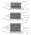
- FIG. 1( a )is a diagrammatic representation of a bistable electrical device in accordance with the present invention that utilizes one buffer layer.
- FIG. 1( b )is a diagrammatic representation of a bistable electrical device in accordance with the present invention that utilizes two buffer layers.
- FIG. 1( c )is a diagrammatic representation of a bistable electrical device in accordance with the present invention that utilizes three buffer layers.
- FIG. 2is a graph of the typical I-V characteristics of a Cu/LiF/AIDCN/Cu device in accordance with the present invention that is initially in the Off-state.
- the switching-on voltageranges from V c1 to V c2 .
- the switching-off voltageis higher than V c2 .
- the read voltageis the less than V c1 .
- FIG. 3is a graph of the I-V characteristics of On-state and Off-state for devices in accordance with the present invention.
- the reading voltageis 0.2 V and the On/Off ratio is about 7 orders in magnitude.
- FIG. 4( a )is a scanning tunneling microscope image of the surface of a 10 ⁇ m ⁇ 10 ⁇ LiF buffer layer (2.5 nm thickness).
- FIG. 4( b )is a scanning tunneling microscope image of the surface of a 1 ⁇ m ⁇ 1 ⁇ m copper layer (100 nm thickness).
- FIG. 5is a schematic diagram of the measurement system used to measure transient responses of exemplary Cu-OBD's in accordance with the present invention.
- FIG. 6( a )is a graph of the transient response of an exemplary Cu-OBD from the Off-state to On-state.
- the response of the devicewas measured by using a 50 Ohm read resistor.
- the response timeis about 28 ms.
- FIG. 6( b )is a graph of the transient response of the On-state of an exemplary Cu-OBD.
- the applied voltage pulsewas 0.38V and 100 ns.
- the device responsewas measured using a 50 Ohm resistor.
- FIG. 7( a )is a graph of the transition speed of an exemplary Cu-OBD from the low resistance state to the high resistance state.
- the “applied pulsed” curverepresents the applied voltage pulse.
- the “device response” curvestands for the device response from On-state to Off-state by a 50 Ohm read resistor. The two current peaks are caused by the capacitor effect (charging and discharging) of the off-state device.
- FIG. 7( b )is a graph of the dynamic response of an exemplary Cu-OBD (initially at On-state) to an applied sharp voltage pulse (3.5 V peak 20 ns half-height width).
- the response of the Cu-OBDwas measured using 50 Ohm read resistor.
- the negative peakindicates that the device already changed to the off state. The transition process is so fast that it could not be recognized by our current measurement systems.
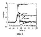
- FIG. 8is a graph of the transient response of both the On-state and Off-state of an exemplary Cu-OBD.
- the On-state responsefollows the applied pulse shape, while the Off-state shows a discharging effect which can be used to determine the device status.
- FIG. 9( a )is a graph of the frequency dependence of capacitance of an exemplary Cu-OBD in the On-and-Off states.
- FIG. 9( b )is a graph of the frequency dependence of the phase angle of impedance of an exemplary Cu-OBD in the On-and-Off states.
- FIG. 10is a schematic diagram of the circuit model used for calculating the devices' capacitance.
- the capacitance of the measurement systemis less than 0.01 pF and is therefore omitted.
- FIG. 11is a graph of the frequency-dependence of the imaginary part of the impedance for the On-state of an exemplary Cu-OBD.
- the line in the graphis the fitting results using formula (3) to fit the experimental data.
- the device's capacitancewas determined to be about 0.3 pF which is the same as the direct measurement shown in FIG. 9( a ).
- FIG. 12is a graph of the frequency-dependence of the imaginary part of the impedance for the Off-state of an exemplary Cu-OBD.
- the line in the graphis the fitting results using formula (4) to fit the experimental data.
- the device's capacitancewas determined to be about 116 pF which is the same as the direct measurement shown in FIG. 9( a ).
- FIG. 13( a )is a schematic diagram of an equivalent circuit for the off-state exemplary Cu-OBD (pure capacitor model).
- FIG. 13( b )is a schematic diagram of an equivalent circuit for the on-state exemplary Cu-OBD from conducting filament formation.
- the resistor in FIG. 13( b )is the filament's resistance.
- FIG. 14is a graph of the frequency-dependence capacitance of an Off-state exemplary Cu-OBD with a resistor (mimics conducting filaments) parallel connected to the Cu-OBD.
- the capacitances with different values of parallel-connected resistorsare the same as single Off-state Cu-OBD's (about 100 pF). This demonstrates the On-state of the exemplary Cu-OBD is not a result of filament formation.
- FIG. 15( a )is a graph of the on-state I-V characteristics for an exemplary Cu-OBD with various active layer areas.
- the bold arrowrepresents an increase in area.
- the “+” lineis 2 mm 2 ; the “solid triangle” line is 1 mm 2 ; the “open square” line is 0.5 mm 2 ; and the “solid square” line is 0.25 mm 2 .
- FIG. 15( b )is a graph of the area-dependence of the on-state current at 0.2 V bias.
- FIG. 16is graph of the I-V characteristics of two exemplary Cu-OBD's with the same LiF layer thickness (2.5 nm), but different organic-layer thickness (45 nm, closed circles, and 100 nm, open circles, respectively).
- the On/Off ratios for the thicker and thinner devicesare 10 8 and 10 3 , respectively.
- FIG. 17( a )is a graph of the I-V behavior of an exemplary Cu-OBD at 80, 160, 220, 250 and 300° K. When the temperature below 250 K the device exhibit non-linear I-V characteristics. Below the switching bias voltage (about 0.92 V), the none-linear I-V curves at the different temperature overlap. The switching voltage is the same at 250 and 300 K.
- FIG. 17( b )is a graph of the On-state I-V curves of an exemplary Cu-OBD at 80, 250 and 300 K. The measurement sequence is, first 300° K, then cool down to 80 K, then heating to 250 K.
- FIG. 18is a graph of the cycles test for an exemplary Cu-OBD.
- the devicewas in the On-state.
- An erase voltage pulsewas applied so that the device changed to Off-state.
- the stability of the On-statewas tested by leaving the device alone for increasing amounts of time (such as 2 hours, 2 days) without any bias, and then measuring current through the device. The device still remained at the On-state as shown in FIG. 18 .
- the On-statecan be erased to the Off-state for continued cycles test.
- the Off-state of the exemplary Cu-OBDwas also stable.
- FIG. 19is a graph of the cycles test for an exemplary Cu-OBD (Cu/LiF(2.5 nm)/AIDCN(45 nm)/Cu).
- a 3V voltage pulsewas used for “switch-off” and a 1.2 V voltage pulse was used for “switch-on”. The current was read at 0.2 V bias.
- FIG. 20is a graph of the heating-treatment and cycles test for an exemplary Cu-OBD.
- the Off-state currentdecreases (about 2 orders in magnitude) after heating treatment.
- the heating treatmenthas no effect on the On-state current of the device.
- This heating effect of the Off-state currentcan only be observed for devices with relatively thinner AIDCN layers in which the Off-state current is relatively high.
- Thisis another method for decreasing the Off-state current of Cu-OBD's.
- FIG. 21 ( a )is a graph of the I-V characteristics of an exemplary Cu-OBD for write-read-erase real time dynamic cycles test.
- FIG. 21( b )is a graph of the real time dynamic Write-Read-Erase cycle test of an exemplary Cu-OBD.
- FIG. 22( a )is a SIMS Cu + depth profile of an exemplary Cu-OBD.
- FIG. 22( b )is a SIMS Cu depth profile of an exemplary Cu-OBD.
- the On-stateis caused by high Cu + concentration within the organic layer.
- FIG. 1An organic bistable electrical device in accordance with the present invention is shown in FIG. 1 .
- the deviceincludes an organic layer 4 that is sandwiched between a first electrode 5 and a second electrode 2 .
- the organic layer 4is shown in the form of a layer. However, it will be understood that the organic layer can be provided in any number of different shapes. Organic layers in the form of a thin layer or film are preferred since fabrication techniques for forming thin films are well known.
- the organic layer 4includes a first surface that is in electrical contact with the first electrode 5 .
- the organic layer 4includes a second surface that is located on the other side of the organic layer 4 and which is in electrical contact with the second electrode 2 .
- the second electrode 2is typically located on an insulating substrate 1 .
- the substrate 1can be either ridged or flexible and made from either organic or inorganic materials that are well-know for use as insulating substrates in electronic devices.
- a buffer layer 3is provided between the second electrode 2 and the organic layer 4 to provide control of metal ion migration into the organic layer 4 .
- the buffer layer 3 on the anode sideis used for a number of purposes.
- the buffer layer 3is used to control metal ion injection from the anode by decreasing the metal ion injection barrier at a proper applied voltage pulse (V c1 ⁇ V ⁇ V c2 ) condition to realize the switch-on process.
- Another purposeis to control metal ion injection from the anode by increasing the copper ion injection barrier at higher applied voltage pulse condition (V>V c2 ) to realize the switch-off process.
- Another purposeis to control metal ion injection from the anode by keeping the metal ion injection properties (either no injection for Off-state or injection for On-state) at a low applied voltage pulse condition to realize the read process.
- the switch-off processcan be defined as the writing-process, while the switch-on process can be defined as the erasing process.
- the organic bistable electrical deviceis typically connected to an electronic control unit via electrical connections to the electrodes (not shown).
- the control unitis capable of providing an electrical voltage bias across the organic layer 4 via the two electrodes 2 and 5 to convert the OBD between low resistance (On) and high resistance (Off) states.
- the control unitis capable of, among other things, measuring current to determine the electrical resistance of the OBD.
- the materials for the electrodes 2 and 5can be metals or conducting materials like indium tin oxide (ITO). Suitable metals for use as the electrodes include copper (Cu), gold (Au), silver (Ag), aluminum (Al) and other metals that have relatively high diffusion coefficients in the organic layer. Copper is a preferred electrode material with devices utilizing at least one copper electrode being referred to as a “Cu-OBD”. Either electrode can be the anode provided that it is copper or a similar metal as set forth above.
- the materials for the buffer layershould be insulating or low conducting materials.
- a variety of low conducting or insulating materialsmay be used to form the particles (in the form of insulating dots or flakes) that make up the buffer layer.
- LiF, NaCl and other compounds similar to LiF and NaClmay be used. Such compounds typically form flakes.
- Metal oxides, such as aluminum oxide (Al 2 O 3 ),may be used. These compounds typically form dots.
- the thickness of the buffer layeris preferably from 1 to 10 nm thick with 2-5 nm being especially preferred. The thickness of the buffer layer can be as great as 50 nm, if desired.
- the buffer layeris composed of small dots or flake-like deposits which are important for the observed electrical bistable behavior. It is preferred that the insulating dots or flakes substantially cover the electrode surface. However, some open spaces should remain between the dots or flakes.
- FIG. 4( a )is an STM image of a 10 ⁇ 10 ⁇ m 2 section of a buffer layer which shows LiF flakes on a copper surface. FIG. 4( a ) shows what is meant by “substantially” covering the electrode surface.
- the degree of surface coverage and size of the flakesmay be varied from what is shown in FIG. 4( a ) provided that the desired properties provided by the buffer layer are not destroyed.
- the degree of surface coverage and flake or dot sizeis related to the thickness of the buffer layer. In general, the thicker the buffer layer, the larger the degree of coverage, and the surface morphology may be varied too.
- the materials for the organic layerare preferably small conjugated low conductivity organic materials.
- Suitable low conductivity materialsinclude organic semiconductors.
- Exemplary organic semiconductorsinclude small molecular organic materials such as 2-amino-4,5-imidazoledicarbonitrile (AIDCN); tris-8-(hydroxyquinoline)aluminum (Alq); 7,7,8,8-tetracyanoquinodimethane (TCNQ); 3-amino-5-hydroxypyrazole (AHP); tris-(8-hydroxyquinolinolato)aluminum (Alq3); and copper or zinc 2,9,16,23-tetra-tert-butyl-29H,31H-phthalocyanine (CuPc or ZnPc).
- inorganic materialslike silicon, gallium, gallium nitride and similar semi-conductors may be used in place of the organic layer.
- the so-called “organic layer”is typically from 10 to 1000 nm thick.
- the various electrodes, organic layers and buffer layers that make up the organic bistable devices of the present inventioncan be fabricated by vacuum thermal evaporation methods, spin-coating or continuous-coating techniques which are all well-known in the electronic device manufacturing field.
- FIG. 1( b )A second example of an OBD device, according to an embodiment of the current invention, is shown schematically in FIG. 1( b ) wherein buffer layers 3 are provided between the organic layer 4 and both electrodes 2 and 5 .
- FIG. 1 ( c )a third alternate embodiment is shown wherein two organic layers 4 are sandwiched between electrodes 2 and 5 . Three buffer layers 3 are used to separate the two organic layers 4 from each other and to separate the electrodes 2 and 5 from the organic layers. As is apparent, a number of different combinations of organic layers with buffer layers and electrodes are possible.
- FIG. 1The basic structure of the exemplary devices is shown in FIG. 1 .
- Cuwas selected for the electrodes due to its high diffusion coefficient (25).
- the buffer layerswere approximately 4 ⁇ m thick (unless otherwise noted) and included dielectric materials, such as lithium fluoride (LiF) and aluminum oxide.
- materials with low conductivity, good film formability and stabilitysuch as 2-amino-4,5-imidazoledicarbonitrile (AIDCN), tris-8-(hydroxyquinoline)aluminum (Alq 3 ), and Zinc 2,9,16,23-tetra-tert-butyl-29H,31H-phthalocyanine (ZnPc) were selected for the organic layers.
- AIDCN2-amino-4,5-imidazoledicarbonitrile
- Alq 3tris-8-(hydroxyquinoline)aluminum
- ZnPcZinc 2,9,16,23-tetra-tert-butyl-29H,31H-phthalocyanine
- the OBD's of the present inventioncan be fabricated by simple vacuum thermal evaporation methods, spin-coating or continuous-coating techniques.
- the Cu-OBD's in these exampleswere fabricated by vacuum thermal evaporation methods. All the depositions were performed in a high vacuum about 1 ⁇ 10 ⁇ 6 torr. A preferred process includes depositing all films for device fabrication without breaking the vacuum.
- the buffer layercontrols Cu ions injection into the organic layer at various applied voltages.
- V c1generally, ranging from 0.2 to 3 V
- V c2generally above 3 V in 10 nanoseconds width
- the two statesdiffer in their electrical conductivity by several orders (3-9) of magnitude depending on the device fabrication processing, and can be precisely switched by controlling the Cu + concentration through the application of external voltage pulses.
- a small voltage pulse(less than 0.1V, ten nanoseconds width) can be used to read.
- On-state and Off-stateare quite stable even being heated to 110° C., which makes it suitable for nonvolatile memory application.
- the On-state current density of the deviceis quite high ( ⁇ 2A/cm 2 @ 0.1V bias).
- the devicesare especially well suited for flash memory applications and for driving light-emitting pixels in display applications.
- FIG. 2shows the typical I-V characteristics of the Cu-OBDs when the device is initially in the Off-state (high impedance), the high conductive state can be excited by a voltage V (V c1 ⁇ V ⁇ V c2 )). Higher voltage (V>V c2 ) can restore the device to the Off-state.
- V c1 ⁇ V ⁇ V c2 )Higher voltage (V>V c2 ) can restore the device to the Off-state.
- the Off-stateis stable if the following applied voltage is less than V c1 .
- V c2Once the device is excited by the small voltage to the On-state, it will remain at the On-state for prolonged periods of time if the following applied voltage is less than V c2 . Therefore, we can use very small voltage (0.1 or 0.2V) to read the On-state and Off-state.
- the On-Off ratio of the devicescan be as high as 7 orders in magnitude (See FIG. 3 ).
- the OBD devicesoperate according to the following principles. Copper that diffuses into other materials is in a positively charged state (26), and the copper ions drift in both silicon (27) and organic materials (28), and cause copper metallization. Generally diffusion barrier layers are used to prevent this metallization (29). The diffusion barrier provides an interface adhesion (or an energy barrier) to prevent Cu + diffusion and metallization (30). For Cu-OBD's, when positive bias is applied, copper is ionized at the inner-face of the anode and acts as the Cu + source. When the energy of Cu + is high enough (larger than eV c1 ) to overcome the energy barrier, they are injected into the organic layer, and drift towards the cathode.
- FIG. 4( a )shows the STM image of an LiF layer with 2.5 nm in thickness on a pre-deposited Cu substrate. It can be seen from FIG. 4( a ) that the deposited LiF layer of dots is flake-like, which is important for the observed electrical bistable behavior.
- FIG. 4( b )shows the STM image of the surface of the deposited Cu electrode layer. It can be seen from FIG. 4( b ) that the surface of the Cu layer is quite smooth compared with the LiF layer, which indicates that the surface structure of LiF shown in FIG. 4( a ) is caused by LiF itself and not the Cu surface morphology.
- the insulating dot or flakessubstantially cover the electrode surface, but that some open spaces remain between the dots or flakes.
- FIG. 4( a )shows what is meant by “substantially” covering the electrode surface. The degree of surface coverage may be varied from what is shown in FIG. 4( a ) provided that the desired properties provided by the nano-layer are not destroyed.
- the thickness of the flake or dot layercan range from 1 to 50 nanometers. Thickness on the order of 2 to 5 nanometers is preferred.
- the transition speed of the Cu-OBDs from both the high-resistance state to low resistance state and from the low-resistance state to the high-resistance stateis measured by transient measurement.
- the measurement setupis shown in FIG. 5 .
- the transition speed of the On-to-Off stateis relatively slow, about several ten milliseconds.
- FIG. 6( a )shows the transient response of a Cu-OBD from the Off-state to the On-state. It can be seen from FIG. 6( a ) that when the voltage pulse is applied to the device, the device initially keeps its high-resistance state. After about a 28 ms delay time, the device jumps to low-resistance state.
- the real transition speed from high to low resistance stateis quite small as shown by in FIG. 6( a ).
- the tens of milliseconds delay timeindicates that Cu + ions travel from the anode to the cathode.
- the electrical behavior of the On-state Cu-OBDis like a pure resistor.
- the transient electrical behavior of the On-state Cu-OBDis shown in FIG. 6( b ). It can be seen from FIG. 6( b ) that no capacitor effects (charging and discharging) are observed for the on-state Cu-OBDs.
- the currentfollows the applied voltage pulse, which indicates that the on-state Cu-OBDs exhibits pure resistor behavior. This conclusion is confirmed by the impedance measurements set forth below.
- FIG. 7( a )shows the transient response of an exemplary Cu-OBD (initially at the low resistance state) to an applied voltage pulse.
- DC I-V curve measurementswere taken to make sure the device was initially at the low resistance state.
- the transition speed from low resistance state to high resistance stateis less than nanoseconds. Therefore, a narrow voltage pulse can be used to excite the devices from the on state to the off state.
- FIG. 7( b )shows the dynamic response of Cu-OBDs (initially at On-state) to a very sharp voltage pulse.
- the transient response of On-state and Off-state of Cu-OBDs to a very sharp applied voltage pulseis quite different as shown in FIG. 8 . It can be seen from FIG. 8 that the current response of the On-state device follows the applied voltage pulse very well, while a negative peak can be seen clearly in the Off-state device response. This is the capacitor discharging effect of the Off-state devices. Therefore, very short voltage pulses (less than 20 ns) can be used for reading. The reading time of a typical Cu-OBD can be less than 20 ns. By further decreasing the device area, the speed of the device will be much faster as the capacitance of the device decreases.
- Impedance measurementswere carried out using an HP 4284A LCR meter.
- the frequency dependence of the device's capacitanceis shown in FIG. 9( a ). If can be seen from FIG. 9( a ) that the Off-state devices' capacitance is about 100 pF, while the On-state devices' capacitance is about 0.3 pF.
- the capacitancedecreased more than 2 orders in magnitude after the device was switched from Off-state to On-state.
- FIG. 9( b )The phase of the impedance for Cu-OBD at both the On-state and the Off-state are shown in FIG. 9( b ). It can be seen from FIG. 9( b ) that the phase is nearly zero for the device in the On-state indicating a pure resistor case. The phase for the device at the Off-state is nearly ⁇ 90°, indicating a pure capacitor case.
- the capacitance data shown in FIG. 9( a )is directly measured by a CPCR mode of the LCR meter. To confirm this data, frequency-dependence impedance data were also measured, from which capacitance can be calculated by a circuit model shown in FIG. 10 . The impedance of this circuit is
- Z ois the amplitude of impedance.
- FIG. 11shows the frequency-dependence of the imaginary part of the impedance of the On-state CU-OBD.
- FIG. 12shows the frequency-dependence of the imaginary part of the impedance of the Off-state Cu-OBD.
- the device's capacitancewas determined to be about 116 pF which is the same as the direct measurement shown in FIG. 9( a ).
- FIG. 13shows the equivalent circuit of the On-state from a conducting filament formation point of view.
- FIG. 14shows the frequency-dependence capacitance of an Off-state Cu-OBD with a resistor parallel connected to it.
- the capacitances with different values of parallel-connected resistorsare the same as single Off-state Cu-OBDs (about 100 pF). As shown in FIG. 9( a ) and FIG.
- the capacitance of the On-state Cu-OBDis much smaller than the Off-state Cu-OBD (more than two orders). Therefore, the section of conducting path for On-state device is the same as the device's area. This would not be the case for filament formation for On-state Cu-OBDs.
- the On-state currenthas little, if any, relation with the device's area if conducting filament formation is involved.
- the On-state I-V characteristics for Cu-OBDs with various devices' areaare shown in FIG. 15( a ).
- the area-dependent of On-state current at 0.2 V biasis shown in FIG. 15( b ).
- the On-state current at the same biasis nearly proportional to the devices' surface area.
- the On/Off ratiois an important factor for device's application.
- the Off-state current of the devicesmay not be low enough. Therefore, determining how to decrease the leakage current and increase the On/Off ration is very important.
- determining how to decrease the leakage current and increase the On/Off rationis very important.
- the thickness of the buffer layer (LiF) and the organic layer (AIDCN)It was found that about 2.5 nm for LiF layer and about 100 nm for the AIDCN layer is the preferred condition to obtain the highest On/Off ratio.
- a 10 8 On/Off ratiohas been achieved for Cu-OBDs.
- the Off-state currentwill go up, leading to a decrease in the On/Off ratio.
- the opened circlesrepresent the data for the Cu-OBD with a thicker AIDCN layer (100 nm).
- the On/Off rationcan reach as high as 10 8 .
- the Off-state currentis within the limitation of the measurement system.
- the closed circlesstand for the data for the Cu-OBD with a thinner AIDCN layer (45 nm).
- the On-state currentis a little higher, but the Off-state current is much larger than the thicker one.
- the On/Off ratio for the Cu-OBD with 45 nm-thickness AIDCN layeris just above 10 3 .
- FIG. 17( a )shows the I-V behavior of a Cu-OBD at 80, 160, 220, 250 and 300° K.
- the switching bias voltageabout 0.92 V
- the switching voltageis the same at 250 and 300° K
- the On-state I-V curves at 80, 250 and 300° Kare shown in FIG. 17( b ).
- the On-state I-V characteristics at 250° Kwere measured. It can be seen from FIG. 17( b ) that there is some thermal hysteretic behavior.
- the On-state of CU-OBDshas a linear I-V relation, indicating that the charge transport in the On-state of the Cu-OBD is not a hopping process.
- the exemplary Cu-OBD's that were preparedwere found to be non-volatile rewritable memory devices. Once a Cu-OBD is switched to either state, it remains at that state without any bias applied for a long time (more than months).
- WRERwrite-read-erase-read
- FIG. 18shows the cycles test for an exemplary Cu-OBD. It should be noted that this cycles test is not a time-dependent dynamic cycles test.
- the real-time dynamic cycles testwill be set forth below. At first, the device was in the On-state with an erase voltage pulse being applied to change the device to the Off-state. The data shown on FIG.
- On-state 18is cycle-number dependent On-and-Off states current at 0.2 V.
- the stability of the On-statewas tested by leaving it alone for some time (such as 2 hours, 2 days) without any bias, then measuring it again. It still remained at the On-state as shown in FIG. 18 .
- the On-statecertainly can be erased to the Off-state for continued cycles test.
- the Off-state of Cu-OBDsis also stable. When the device was switched to the Off-state and kept in vacuum chamber for 37 days, it was still at the Off-state and could be switched to the On-state for further continuous cycles testing (see the last three dots at the right side of FIG. 18 ).
- FIG. 19shows another Cu-OBD (Cu/LiF(2.5 nm)/AIDCN(45 nm)/Cu) cycles test. 3V was used for erase, 1.2 V for write, and the current was read at 0.2 V bias. It can be seen from FIG. 19 that the On-state current is nearly the same during the cycles test, but the Off-state current shows decreasing tendency during cycles test.
- FIG. 20shows the heating-treatment and cycles test.
- the devicewas at On-state, as shown by the first dot in FIG. 20 , then it was heated to 110° C. for 1 minute. After this heating treatment, it was still at the On-state as shown by the second dot in FIG. 20 . Then, a 3 V voltage pulse was applied to restore it to the Off-state.
- the third dot in FIG. 20shows that the device was successfully restored to the Off-state that was then switched to On-state again by applying a 1.2 V voltage pulse as confirmed by the fourth dot in FIG.
- the Off-state currentdecreases substantially (about 2 order in magnitude) after heating treatment, while heating treatment has no effect on the On-state current of the device.
- This Heating effect of the Off-state currentcan only be observed for devices with relatively thinner AIDCN layer in which the Off-state current is relatively high. This is another method for decreasing the Off-state current of Cu-OBD's.
- FIGS. 21( a ) and ( b )A Keithley 2400 was used to apply programmable voltage pulses in order to conduct WRER cycles tests.
- the typical WRER cycles cellare shown in FIGS. 21( a ) and ( b ).
- FIG. 21( a )is the I-V characteristics for the cycles-test Cu-OBD.
- FIG. 21( b )is the real time dynamic cycles test.
- the On-state and Off-statesare due to the Cu + distribution and subsequent metallization and de-metallization or the organic layer as controlled by the buffer layer.
- This beliefis supported by the secondary ion mass spectrometry (SIMS) depth profile measurement for Cu + ion and Cu atom in exemplary devices in both states. It was found that Cu + ion are driven into the organic layer in the On-state (metallization process), while Cu + ions drifted out of the organic layer in the Off-state as shown in FIG. 22( a ) (de-metallization process). Therefore, the ON-and-OFF states can be switched back and forth by controlling the Cu + ion distribution profile within the organic layer.
- SIMSsecondary ion mass spectrometry
- the atomic Cu distribution in the Cu-OBDs( FIG. 22( b )) was found to be low within the organic layer for both of the states. Accordingly, the dynamic Cu + concentration within the organic layer is believed to be responsible for the observed bistability of Cu-OBDs.
- the buffer layers (nanosurfaces) of the present inventionmay be used in a wide variety of bistable devices as an interface between the electrode and the organic bistable layer.
- the active layer of the present OBD'sorganic layer plus one or more buffer layers
- the present inventionis not limited to the above preferred embodiments and examples, but is only limited by the following claims.
Landscapes
- Engineering & Computer Science (AREA)
- Chemical & Material Sciences (AREA)
- Physics & Mathematics (AREA)
- Nanotechnology (AREA)
- Spectroscopy & Molecular Physics (AREA)
- Materials Engineering (AREA)
- Mathematical Physics (AREA)
- Theoretical Computer Science (AREA)
- Crystallography & Structural Chemistry (AREA)
- Semiconductor Memories (AREA)
Abstract
Description
Zosin(θ)=−2πr2cf. (3)
Here, Zois the amplitude of impedance.
Zosin(θ)=−1/(2πcf). (4)
- 1. J. F. Dewald, A. D. Pearson, W. R. Northover, and W. F. Peck, Jr., J. Electrochem. Soc., 109, 243c (1962). “Semi-conducting glasses”
- 2. Ovshinsky, S. R. Localized states in the gap of amorphous semiconductors. Phys. Rev. Lett., vol. 36 (no. 24), 14 Jun. 1976, p. 1469-72.
- 3. Yu, G. Kriger, N. F. Yudanov, I. K., Igumenov, and S. B. Vashchenko, J. Struct. Chem., 34 (1993). “Study of test structures of a molecular memory element”
- 4. H. J. Hovel and J. J. Urgell, J. Appl. Phys. 42, 5076 (1971). “Switching and memory characteristics of ZnSe—Ge heterojunctions”
- 5. R. Kumai, Y. Olimoto and Y. Tokura, Science, 284, 1645 (1999). “Current-induced insulator-metal transition and pattern formation in an organic charge-transfer complex”.
- 6. R. S. Potember, T. O. Poehler and D. O. Cowan, Appl. Phys. Lett. 34, 407 (1979). “Electrical switching and memory phenomena in Cu-TCNQ thin films”
- 7. F. Garnier, R. Hajlaoui, A. Yassar, and P. Shirakawa, Science 265, 1684 (1994)
- 8. F. Hide, M. A. Diaz-Garcia, B. J. Schwartz, M. R. A. Andersson, Q. Pei, and A. J. Heeger, Science 273, 1883 (1997).
- 9. R. Kumai, Y. Okimoto, Y. Tokura, Science 284, 1645 (1999).
- 10. W. Fujita, and K. Awaga, Science 286, 261 (1999).
- 11. J. H. Burroughes, D. D. C. Bradley, A. R. Brown, R. N. Marks, K. Mackay, R. H. Friend, P. L. Burn, and A. B. Holmes, Nature, 347, 539 (1990).
- 12. T. Yamada, D. Zou, H. Jeong, Y. Akaki, and T. Tsutsui, Synthetic Metals, 111-112, 237 (2000).
- 13. J. Liu, Y. Shi, L. P. Ma, and Y. Yang, J. Appl. Phys. 88, 605 (2000).
- 14. Y. Hamada, C. Adachi, T. Tsutsui, S. Saito, Jpn. J. Appl. Phys. 31, 1812 (1992).
- 15. Y. Yang et al., U.S. Pat. No. 5,563,424, Oct. 8, 1996.
- 16. McBrayer, J. D., Swanson, R. M., and Sigmon, T. W., Diffusion of metals in silicon dioxide.J. Electrochem. Soc.133, 1242(1986).
- 17. Rosenberg, R., Edelstein, D. C., Hu, C. K., Rodbell, K. P., Copper metallization for high performance silicon technology, Annual Rev. Materials Science, 30, 229 (2000). Kaloyeros, A. E., Eisenbraun, E., Ultrathin diffusion barriers/liners for gigascale copper metallization, Annual Rev. Materials Science, 30, 363(2000).
- 18. W. D. Brown, J. E. Brewer, Nonvolatile semiconductor memory technology, IEEE Press, New York, (1998).
- 19. Ma, L. P., Pyo, S. M., Xu, Q. F. and Yang, Y., Nonvolatile electrical bistability of organic/metal-nanocluster/organic system, Appl. Phys. Lett. 82, 1419(2003), Ma, L. P., Liu, J, and Yang, Y., organic electrical bistable devices and rewritable memory cells, Appl. Phys. Lett. 80, 2997 (2002), Ma, L. P. Liu, J., Pyo, S. M. and Yang, Y., Organic bistable light-emitting devices, Appl. Phys. Lett. 80, 362(2002), Ma, L. P., Liu, J., Pyo, S. M., Xu, Q. F. and Yang, Y., Organic bistable devices, Mol. Cryst. Liq. Cryst. 378, 185(2002).
- 20. Nakayama, K., Kojima, K., Imai, Y., Kasai, T., Fukushima, S., Kitagawa, A., Kumeda, M., Kakimoto, Y., Suzuki, M., Nonvolatile memory based on phase change in Se—Sb—Te glass, J. J. Appl. Phys.,
Part 1, 42 (2A), 404(2003). - 21. Kozicki, M. N. and West, W. C., Programmable metallization cell structure and method of making same, U.S. Pat. No. 5,761,115 (1998).
- 22. Ostraat, M. L., De Blauwe, J. W., Green, M. L., Bell, L. D., Brongerma, M. L., Casperson, J. R., Flagan, C. and Atwater, H. A., Synthesis and characterization of aerosol silicon nanocrystal nonvolatile floating-gate memory devices, Appl. Phys. Lett. 79, 433(2001).
- 23. Ma, L. P., Yang, W. J., Xie, S. S. and Pang, S. J., Ultrahigh density data storage from local polymerization by a scanning tunneling microscope, Appl. Phys. Lett. 73, 3303(1998).
- 24. Segui, Y., Bui Ai, and Carchano, H., Switching in polystyrene films: Transition from on to off state, J. Appl. Phys. 47, 140(1976).
- 25. J. Chen, W. Wang, M. A. Reed, A. M. Rawlett, D. W. Price, and J. M. Tour, Room-temperature negative differential resistance in nanoscale molecular junctions, Appl. Phys. Lett. 77, 1224(2000).
- 26. Beeler, F., Andersen, O. K, and Scheffler, M., Theoretical Evidence for Low-Spin Ground States of Early Interstitial and Late Substitutional 3d Transition-Metal Ions in Silicon, Phys. Rew. Lett. 55, 1498(1985).
- 27. Istratov, A. A., Weber, E. R, Physics of copper in silicon, J. Electrochemical Society, 149, G21(2002). Istratov, A. A., Flink, C., Hieslmair, H., McHugo, S. A., Weber, E. R., Diffusion, solubility and gettering of copper in silicon, Materials Science. and Engineering Technology B, 72, 99(2000). Lee, K. L., Hu, C. K, Tu, K. N., In-situ scanning electron microscope comparison studies on electromigration of Cu and Cu(Sn) alloys for advanced chip interconnects, J. Appl. Phys. 78, 4428-4437(1995).
- 28. Loke, A. L. S., Wetzel, J. T., Townsend, P. H., Tanabe, T., Vrtis, R. N., Zussman, M. P., Kumar, D., Ryu, C., Wong, S. S., Kinetics of copper drift in low-kappa polymer interlevel dielectrics, IEEE Transactions on Electron Devices, 46, 2178(1999).
- 29. Wang, M. T., Lin, Y. C., Chen, M. C., Barrier properties of very thin Ta and TaN layers against copper diffusion, J. Electrochemical Society, 145, 2538(1998). Faltermeier. C., Goldberg, C., Jones, M., Upham, A., Manger, D., Peterson, G., Lau, J., Kaloyeros, A. E., Arkles, B., Paranjpe, A., Barrier properties of titanium nitride films grown by low temperature chemical vapor deposition from titanium tetraiodide, J. Electrochemical Scoiety, 144, 1002(1997). Krishnamoorthy, A., Chanda, K., Murarka, S. P., Ramanath G., Ryan, J. G., Self-assembled near-zero-thickness molecular layers as diffusion barriers for Cu metallization, Appl. Phys. Lett. 78, 2467(2001).
- 30. Lane, M. W., Liniger, E. G., and Lioyd, J. R., Relationship between interfacial adhesion and electromigration in Cu metallization, J. Appl. Phys. 93, 1417(2003).
- 31. Istratov, A. A., Flink, C., Hieslmair, H., Weber, E. R., and Heiser, T., Intrinsic diffusion coefficient of interstitial copper in silicon, Phys. Rev. Lett. 81, 1243(1998).
- 33. Sprang, H. A. van, and Venne, J. L. M. van de, Influence of the surface interaction on threshold values in the cholestericnematic phase transition, J. Appl. Phys. 57, 175(1985). Boyd, G. D., Cheng, J, and Ngo, P. D. T., liquid-crystal orientational bistability and nematic storage effects, Appl. Phys., Lett. 36, 556(1980), Gruler, H., and Cheung, L., Dielectric alignment in an electrically conducting nematic liquid crystal, J. Appl. Phys. 46, 5097(1975). Patel, J. S., Room-temperature switching behavior of ferroelectric liquid c2ystals in thin cells, Appl. Phys. Lett. 47, 1277(1985).
- 33. Yang, K. H., Chieu, T. C., and Osofsky, S., Depolarization field and ionic effects on the bistability of surface-stabilized ferroelectric liquid-crystal devices, Appl. Phys. Lett. 55, 125(1989).
Claims (14)
Priority Applications (1)
| Application Number | Priority Date | Filing Date | Title |
|---|---|---|---|
| US10/542,843US7482621B2 (en) | 2003-02-03 | 2004-02-02 | Rewritable nano-surface organic electrical bistable devices |
Applications Claiming Priority (3)
| Application Number | Priority Date | Filing Date | Title |
|---|---|---|---|
| US44474803P | 2003-02-03 | 2003-02-03 | |
| US10/542,843US7482621B2 (en) | 2003-02-03 | 2004-02-02 | Rewritable nano-surface organic electrical bistable devices |
| PCT/US2004/002932WO2004070789A2 (en) | 2003-02-03 | 2004-02-02 | Rewritable nano-surface organic electrical bistable devices |
Publications (2)
| Publication Number | Publication Date |
|---|---|
| US20060131560A1 US20060131560A1 (en) | 2006-06-22 |
| US7482621B2true US7482621B2 (en) | 2009-01-27 |
Family
ID=32850918
Family Applications (1)
| Application Number | Title | Priority Date | Filing Date |
|---|---|---|---|
| US10/542,843Expired - Fee RelatedUS7482621B2 (en) | 2003-02-03 | 2004-02-02 | Rewritable nano-surface organic electrical bistable devices |
Country Status (2)
| Country | Link |
|---|---|
| US (1) | US7482621B2 (en) |
| WO (1) | WO2004070789A2 (en) |
Cited By (8)
| Publication number | Priority date | Publication date | Assignee | Title |
|---|---|---|---|---|
| US20070007513A1 (en)* | 2005-05-20 | 2007-01-11 | Stmicroelectronics S.R.L. | Organic electrically bistable material and its use for producing a memory switch |
| US20090065769A1 (en)* | 2005-04-27 | 2009-03-12 | Semiconductor Energy Laboratory Co., Ltd. | Semiconductor device amd method for manufacturing the same |
| US20090091003A1 (en)* | 2005-10-19 | 2009-04-09 | Electronics And Telecommunications Research | Insulator undergoing abrupt metal-insulator transition, method of manufacturing the insulator, and device using the insulator |
| US20090140231A1 (en)* | 2005-04-27 | 2009-06-04 | Semiconductor Energy Labortory Co., Ltd. | Semiconductor device and method of manufacturing the same |
| US20100065814A1 (en)* | 2008-09-16 | 2010-03-18 | The University Of Hong Kong | Hybrid organic/nanoparticle devices |
| US20130099190A1 (en)* | 2011-10-20 | 2013-04-25 | Samsung Electronics Co., Ltd. | Non-volatile memory device and method of fabricating the same |
| US9755169B2 (en) | 2012-07-27 | 2017-09-05 | Iucf-Hyu | Nonvolatile memory device |
| US9786848B2 (en) | 2010-10-14 | 2017-10-10 | University Of Utah Research Foundation | Nanofiber-based heterojunction approach for high photoconductivity on organic materials |
Families Citing this family (14)
| Publication number | Priority date | Publication date | Assignee | Title |
|---|---|---|---|---|
| TWI229937B (en)* | 2004-06-10 | 2005-03-21 | Ind Tech Res Inst | Organic bistable devices and manufacturing method thereof |
| GB2437188A (en)* | 2004-10-28 | 2007-10-17 | Univ California | Organic-complex thin film for nonvolatile memory applications |
| US7776682B1 (en)* | 2005-04-20 | 2010-08-17 | Spansion Llc | Ordered porosity to direct memory element formation |
| US20060245235A1 (en)* | 2005-05-02 | 2006-11-02 | Advanced Micro Devices, Inc. | Design and operation of a resistance switching memory cell with diode |
| TWI304213B (en)* | 2006-01-11 | 2008-12-11 | Ind Tech Res Inst | Organic memory device and method of fabricating the same |
| US20100213411A1 (en)* | 2006-01-17 | 2010-08-26 | Ken Hosoya | Monolith separation medium for chromatography and process for producing the same |
| KR100777419B1 (en) | 2006-11-14 | 2007-11-20 | 한양대학교 산학협력단 | Organic bistable memory device and manufacturing method thereof |
| KR100921506B1 (en)* | 2007-04-24 | 2009-10-13 | 한양대학교 산학협력단 | Display and method of driving the same |
| US20090008633A1 (en)* | 2007-04-25 | 2009-01-08 | Samsung Electronics Co., Ltd. | Nonvolatile memory device using conductive organic polymer having nanocrystals embedded therein and method of manufacturing the nonvlatile memory device |
| AT507620B1 (en)* | 2008-10-07 | 2014-02-15 | Nanoident Technologies Ag | MOBILE DATA STORAGE |
| KR101460165B1 (en)* | 2011-02-18 | 2014-11-11 | 한양대학교 산학협력단 | Nonvolatile memory device |
| KR101485507B1 (en) | 2014-09-25 | 2015-01-26 | 한양대학교 산학협력단 | Nonvolatile memory device |
| CN105336854B (en)* | 2015-09-29 | 2018-05-18 | 北京交通大学 | One kind is based on Whote-wet method silver symmetry electrode electrostrictive polymer bistable device |
| WO2019083899A1 (en)* | 2017-10-23 | 2019-05-02 | Printed Energy Pty Ltd | Thin film self-switching device |
Citations (42)
| Publication number | Priority date | Publication date | Assignee | Title |
|---|---|---|---|---|
| US3719933A (en) | 1970-04-02 | 1973-03-06 | Matsushita Electric Industrial Co Ltd | Memory device having lead dioxide particles therein |
| US3833894A (en) | 1973-06-20 | 1974-09-03 | Ibm | Organic memory device |
| US4144418A (en) | 1977-05-27 | 1979-03-13 | General Electric Company | Voltage responsive switch |
| US4371883A (en) | 1980-03-14 | 1983-02-01 | The Johns Hopkins University | Current controlled bistable electrical organic thin film switching device |
| US4507672A (en)* | 1980-03-14 | 1985-03-26 | The Johns Hopkins University | Method of fabricating a current controlled bistable electrical organic thin film switching device |
| US4652894A (en) | 1980-03-14 | 1987-03-24 | The Johns Hopkins University | Electrical organic thin film switching device switching between detectably different oxidation states |
| US4663270A (en) | 1984-04-25 | 1987-05-05 | The Johns Hopkins University | Multistate optical switching and memory using an amphoteric organic charge transfer material |
| US4987023A (en) | 1988-03-29 | 1991-01-22 | Kabushiki Kaisha Toshiba | Organic thin-film device |
| US5075738A (en)* | 1988-03-28 | 1991-12-24 | Canon Kabushiki Kaisha | Switching device and method of preparing it |
| US5136212A (en) | 1988-02-18 | 1992-08-04 | Canon Kabushiki Kaisha | Electron emitting device, electron generator employing said electron emitting device, and method for driving said generator |
| US5238607A (en) | 1992-02-28 | 1993-08-24 | E. I. Du Pont De Nemours And Company | Photoconductive polymer compositions and their use |
| US5543631A (en)* | 1993-06-17 | 1996-08-06 | Weinberger; Lester | Hybrid organic-inorganic bistable nonlinear optical gate |
| US5563424A (en) | 1994-03-24 | 1996-10-08 | Uniax Corporation | Polymer grid triodes |
| US5569565A (en) | 1991-05-23 | 1996-10-29 | Matsushita Electric Industrial Co., Ltd. | Hologram recording material |
| US5610898A (en) | 1991-07-17 | 1997-03-11 | Canon Kabushiki Kaisha | Information recording/reproducing method for recording and/or reproducing information on information recording carrier by use of probe electrode |
| US5761115A (en) | 1996-05-30 | 1998-06-02 | Axon Technologies Corporation | Programmable metallization cell structure and method of making same |
| US6015631A (en) | 1996-10-07 | 2000-01-18 | Samsung Display Devices Co., Ltd. | Luminescent compound for an electroluminescence display device |
| US6055180A (en) | 1997-06-17 | 2000-04-25 | Thin Film Electronics Asa | Electrically addressable passive device, method for electrical addressing of the same and uses of the device and the method |
| US6122031A (en) | 1996-02-09 | 2000-09-19 | Canon Kabushiki Kaisha | Liquid crystal device and liquid crystal apparatus including same |
| US6208553B1 (en) | 1999-07-01 | 2001-03-27 | The Regents Of The University Of California | High density non-volatile memory device incorporating thiol-derivatized porphyrins |
| US6229047B1 (en) | 1995-12-04 | 2001-05-08 | The Curators Of The University Of Missouri | Dipole aligned NLO chromophores |
| WO2001071814A1 (en) | 2000-03-23 | 2001-09-27 | Japan Science And Technology Corporation | METHOD FOR PREPARING LOW-RESISTANT p-TYPE SrTiO¿3? |
| US20020010261A1 (en) | 1999-02-26 | 2002-01-24 | Callahan Robert W. | Polymer matrix material |
| US20020031602A1 (en)* | 2000-06-20 | 2002-03-14 | Chi Zhang | Thermal treatment of solution-processed organic electroactive layer in organic electronic device |
| WO2002037500A1 (en)* | 2000-10-31 | 2002-05-10 | The Regents Of The University Of California | Organic bistable device and organic memory cells |
| US20020163828A1 (en) | 2001-05-07 | 2002-11-07 | Coatue Corporation | Memory device with a self-assembled polymer film and method of making the same |
| US20020163831A1 (en) | 2001-05-07 | 2002-11-07 | Coatue Corporation | Molecular memory cell |
| WO2002091496A2 (en) | 2001-05-07 | 2002-11-14 | Advanced Micro Devices, Inc. | Reversible field-programmable electric interconnects |
| US20020195600A1 (en) | 2001-05-31 | 2002-12-26 | Rainer Leuschner | Memory element with molecular or polymeric layers, memory cell, memory array, and smart card |
| US20030053350A1 (en) | 2001-08-13 | 2003-03-20 | Krieger Juri H. | Memory device |
| US20030063362A1 (en)* | 2001-10-01 | 2003-04-03 | Demir Hilmi Volkan | Semiconductor device for rapid optical switching by modulated absorption |
| US6600473B1 (en)* | 1999-01-20 | 2003-07-29 | Fuji Xerox Co., Ltd. | Photoconductive switching element, device using it, and apparatus, recording apparatus, and recording method in which the device is incorporated |
| US20030155602A1 (en) | 2001-08-13 | 2003-08-21 | Coatue Corporation | Memory device |
| US20030173612A1 (en) | 2001-08-13 | 2003-09-18 | Krieger Juri H. | Memory device with active and passive layers |
| US20030178667A1 (en) | 2001-08-13 | 2003-09-25 | Krieger Juri H. | Memory device |
| US6631085B2 (en) | 2000-04-28 | 2003-10-07 | Matrix Semiconductor, Inc. | Three-dimensional memory array incorporating serial chain diode stack |
| US20040026714A1 (en) | 2001-08-13 | 2004-02-12 | Krieger Juri H. | Memory device with active passive layers |
| WO2004064074A1 (en) | 2003-01-09 | 2004-07-29 | Polyic Gmbh & Co. Kg | Organo-resistive memory |
| US6774880B2 (en) | 2000-06-13 | 2004-08-10 | Fuji Xerox Co., Ltd. | Photo-addressable type recording display apparatus |
| US6828685B2 (en) | 2002-06-14 | 2004-12-07 | Hewlett-Packard Development Company, L.P. | Memory device having a semiconducting polymer film |
| US6852555B1 (en) | 1999-04-22 | 2005-02-08 | Thin Film Electronics Asa | Method in the fabrication of organic thin-film semiconducting devices |
| US20050111071A1 (en) | 2003-10-07 | 2005-05-26 | Kyoko Kojima | Information-recording medium and method |
- 2004
- 2004-02-02WOPCT/US2004/002932patent/WO2004070789A2/enactiveApplication Filing
- 2004-02-02USUS10/542,843patent/US7482621B2/ennot_activeExpired - Fee Related
Patent Citations (48)
| Publication number | Priority date | Publication date | Assignee | Title |
|---|---|---|---|---|
| US3719933A (en) | 1970-04-02 | 1973-03-06 | Matsushita Electric Industrial Co Ltd | Memory device having lead dioxide particles therein |
| US3833894A (en) | 1973-06-20 | 1974-09-03 | Ibm | Organic memory device |
| US4144418A (en) | 1977-05-27 | 1979-03-13 | General Electric Company | Voltage responsive switch |
| US4371883A (en) | 1980-03-14 | 1983-02-01 | The Johns Hopkins University | Current controlled bistable electrical organic thin film switching device |
| US4507672A (en)* | 1980-03-14 | 1985-03-26 | The Johns Hopkins University | Method of fabricating a current controlled bistable electrical organic thin film switching device |
| US4652894A (en) | 1980-03-14 | 1987-03-24 | The Johns Hopkins University | Electrical organic thin film switching device switching between detectably different oxidation states |
| US4663270A (en) | 1984-04-25 | 1987-05-05 | The Johns Hopkins University | Multistate optical switching and memory using an amphoteric organic charge transfer material |
| US5136212A (en) | 1988-02-18 | 1992-08-04 | Canon Kabushiki Kaisha | Electron emitting device, electron generator employing said electron emitting device, and method for driving said generator |
| US5075738A (en)* | 1988-03-28 | 1991-12-24 | Canon Kabushiki Kaisha | Switching device and method of preparing it |
| US4987023A (en) | 1988-03-29 | 1991-01-22 | Kabushiki Kaisha Toshiba | Organic thin-film device |
| US5569565A (en) | 1991-05-23 | 1996-10-29 | Matsushita Electric Industrial Co., Ltd. | Hologram recording material |
| US5610898A (en) | 1991-07-17 | 1997-03-11 | Canon Kabushiki Kaisha | Information recording/reproducing method for recording and/or reproducing information on information recording carrier by use of probe electrode |
| US5238607A (en) | 1992-02-28 | 1993-08-24 | E. I. Du Pont De Nemours And Company | Photoconductive polymer compositions and their use |
| US5543631A (en)* | 1993-06-17 | 1996-08-06 | Weinberger; Lester | Hybrid organic-inorganic bistable nonlinear optical gate |
| US5563424A (en) | 1994-03-24 | 1996-10-08 | Uniax Corporation | Polymer grid triodes |
| US6229047B1 (en) | 1995-12-04 | 2001-05-08 | The Curators Of The University Of Missouri | Dipole aligned NLO chromophores |
| US6122031A (en) | 1996-02-09 | 2000-09-19 | Canon Kabushiki Kaisha | Liquid crystal device and liquid crystal apparatus including same |
| US5761115A (en) | 1996-05-30 | 1998-06-02 | Axon Technologies Corporation | Programmable metallization cell structure and method of making same |
| US6015631A (en) | 1996-10-07 | 2000-01-18 | Samsung Display Devices Co., Ltd. | Luminescent compound for an electroluminescence display device |
| US6055180A (en) | 1997-06-17 | 2000-04-25 | Thin Film Electronics Asa | Electrically addressable passive device, method for electrical addressing of the same and uses of the device and the method |
| US6600473B1 (en)* | 1999-01-20 | 2003-07-29 | Fuji Xerox Co., Ltd. | Photoconductive switching element, device using it, and apparatus, recording apparatus, and recording method in which the device is incorporated |
| US20020010261A1 (en) | 1999-02-26 | 2002-01-24 | Callahan Robert W. | Polymer matrix material |
| US6852555B1 (en) | 1999-04-22 | 2005-02-08 | Thin Film Electronics Asa | Method in the fabrication of organic thin-film semiconducting devices |
| US6208553B1 (en) | 1999-07-01 | 2001-03-27 | The Regents Of The University Of California | High density non-volatile memory device incorporating thiol-derivatized porphyrins |
| WO2001071814A1 (en) | 2000-03-23 | 2001-09-27 | Japan Science And Technology Corporation | METHOD FOR PREPARING LOW-RESISTANT p-TYPE SrTiO¿3? |
| US6631085B2 (en) | 2000-04-28 | 2003-10-07 | Matrix Semiconductor, Inc. | Three-dimensional memory array incorporating serial chain diode stack |
| US6774880B2 (en) | 2000-06-13 | 2004-08-10 | Fuji Xerox Co., Ltd. | Photo-addressable type recording display apparatus |
| US20020031602A1 (en)* | 2000-06-20 | 2002-03-14 | Chi Zhang | Thermal treatment of solution-processed organic electroactive layer in organic electronic device |
| WO2002037500A1 (en)* | 2000-10-31 | 2002-05-10 | The Regents Of The University Of California | Organic bistable device and organic memory cells |
| US6950331B2 (en)* | 2000-10-31 | 2005-09-27 | The Regents Of The University Of California | Organic bistable device and organic memory cells |
| US20020163828A1 (en) | 2001-05-07 | 2002-11-07 | Coatue Corporation | Memory device with a self-assembled polymer film and method of making the same |
| US20020163831A1 (en) | 2001-05-07 | 2002-11-07 | Coatue Corporation | Molecular memory cell |
| WO2002091496A2 (en) | 2001-05-07 | 2002-11-14 | Advanced Micro Devices, Inc. | Reversible field-programmable electric interconnects |
| US20020195600A1 (en) | 2001-05-31 | 2002-12-26 | Rainer Leuschner | Memory element with molecular or polymeric layers, memory cell, memory array, and smart card |
| US20040026714A1 (en) | 2001-08-13 | 2004-02-12 | Krieger Juri H. | Memory device with active passive layers |
| US20030178667A1 (en) | 2001-08-13 | 2003-09-25 | Krieger Juri H. | Memory device |
| US20030179633A1 (en) | 2001-08-13 | 2003-09-25 | Krieger Juri H. | Memory device |
| US20040026729A9 (en)* | 2001-08-13 | 2004-02-12 | Coatue Corporation | Memory device |
| US20030173612A1 (en) | 2001-08-13 | 2003-09-18 | Krieger Juri H. | Memory device with active and passive layers |
| US20030053350A1 (en) | 2001-08-13 | 2003-03-20 | Krieger Juri H. | Memory device |
| US20040159835A1 (en) | 2001-08-13 | 2004-08-19 | Krieger Juri Heinrich | Memory device |
| US20040160801A1 (en) | 2001-08-13 | 2004-08-19 | Krieger Juri Heinrich | Active programming and operation of a memory device |
| US20030155602A1 (en) | 2001-08-13 | 2003-08-21 | Coatue Corporation | Memory device |
| US20040246768A1 (en) | 2001-08-13 | 2004-12-09 | Krieger Juri Heinrich | Memory cell |
| US20030063362A1 (en)* | 2001-10-01 | 2003-04-03 | Demir Hilmi Volkan | Semiconductor device for rapid optical switching by modulated absorption |
| US6828685B2 (en) | 2002-06-14 | 2004-12-07 | Hewlett-Packard Development Company, L.P. | Memory device having a semiconducting polymer film |
| WO2004064074A1 (en) | 2003-01-09 | 2004-07-29 | Polyic Gmbh & Co. Kg | Organo-resistive memory |
| US20050111071A1 (en) | 2003-10-07 | 2005-05-26 | Kyoko Kojima | Information-recording medium and method |
Non-Patent Citations (90)
| Title |
|---|
| A. Bandyopadhyay and A.J. Pal, Appl. Phys. Lett. 82, 1215 (2003). |
| Adams, David M. et al., "Charge Transfer on the Nanoscale: Current Status", J. Phys. Chem. B., 2003, vol. 107, No. 28, pp. 6668-6697. |
| Bachtold, Adrian et al., "Logic Circuits with Carbon Nanotube Transistors", Science, vol. 294, Nov. 9, 2001, pp. 1317-1320. |
| Baldo, Marc et al., "Organic Vapor Phase Deposition", Adv. Mater. 1998, 10, No. 18, p. 1505-1514. |
| Beeler, F., O.K. Andersen and M. Scheffler", Theoretical Evidence for Low-Spin Ground States of Early Interstitial and Late Substitutional 3d Transition-Metal Ions in Silicon", Phys. Rew. Lett. 55, 1498 (1985). |
| Beinhoff, et al., Poybiphenymethylenes: New Polymers for Bistable Organic Switches; Polymeric Materials: Science and Engineering 90, (2004) 211, 212, U.S. |
| Boyd, G.D., J. Cheng and P.D.T. Ngo, "Liquid-Crystal Orientational Bistability and Nematic Storage Effects", Appl. Phys., Lett. 36, 556 (1980). |
| Bozano, et al; Mechanism for Bistability in Organic Memory Elements; Applied Physics Letters, (2004); vol. 84, No. 4, pp. 607-609; 2004 American Institute of Physics. |
| Brown, W.D. and J.E. Brewer, "Nonvolatile Semiconductor Memory Technology", IEEE Press, New York (1998). |
| Bryce, Martin R., "Tetrathiafulvalenes as pi-Electron Donors for Intramolecular Charge-Transfer Materials", Advanced Materials, 1999, 11, No. 1, p. 11-23. |
| Burroughes, J.H., D.D.C. Bradley, A.R. Brown, R.N. Marks, K. Mackay, R.H. Friend, P.L. Burn and A.B. Holmes, "Light-Emitting Diodes Based on Conjugated Polymers", Nature, vol. 347, p. 539 (1990). |
| Carchano, H. et al., "Bistable Electrical Switching in Polymer Thin Films", Applied Physics Letters, vol. 19, No. 19, Nov. 15, 1971, p. 414-415. |
| Chen, J., W. Wang, M.A. Reed, A.M. Rawlett, D.W. Price and J.M. Tour, "Room-Temperature Negative Differential Resistance in Nanoscale Molecular Junctions", Appl. Phys. Lett. 77, 1224 (2000). |
| Chen, Shaowei et al., "Gold Nanoelectrodes of Varied Size: Transition to Molecule-Like Charging", Science, vol. 280, Jun. 26, 1998, pp. 2098-2101. |
| Chen, Y., et al, Appl. Phys. Lett. 82, 1610 (2003). "Nanoscale molecular-switch devices fabricated by imprint lithography". |
| Chiang, J.C., et al., Synth. Met. 13, 193, (1986). "Polyaniline: Protonic acid doping of the emeraldine form to the metallic regime." |
| D.M. Taylor and C. A. Mills, J. Appl. Phys. 90, 306 (2001). |
| Dewald, J.F., A.D. Pearson, W.R. Northover and W.F. Peck, Jr., "Semi-Conducting Glasses", Electrochem. Soc., 109, 243c (1962). |
| Duan, Xiangfeng et al., "Indium Phosphide Nanowires as Building Blocks for Nanoscale Electronic and Optoelectronic Devices", Nature, vol. 49, Jan. 4, 2001, pp. 66-69. |
| Faltermeier, C., C. Goldberg, M. Jones, A. Upham, D. Manger, G. Peterson, J. Lau, A.E. Kaloyeros, B. Arkles, and A. Paranjpe, "Barrier Properties of Titanium Nitride Films Grown by Low Temperature Chemical Vapor Deposition from Titanium Tetraoidide", J. Electrochemical Society, 144, 1002 (1997). |
| Friend, R.H. et al., "Electroluminescence in Conjugated Polymers", Nature, vol. 397, Jan. 14, 1999, p. 121-128. |
| Fujita, W. and K. Awaga, "Room-Temperature Magnetic Bistability in Organic Radical Crystals", Science, vol. 286 p. 261 (1999). |
| Furukawa, T., Adv. Colloid Interface Sci., 71-72, 183 (1997). "Structure and functional properties of ferroelectric polymer". |
| Garnier, F., R. Hajlaoui, A. Yassar and P. Shirakawa, "All-Polymer Field-Effect Transistor Realized by Printing Techniques", Science 265, 1684 (1994). |
| Gruler, H. and L. Cheung, "Dielectric Alignment in an Electrically Codnucting Nematic Liquid Crystal", J. Appl. Phys. 46, 5097 (1975). |
| Gudiksen, Mark S. et al., "Growth of Nanowire Superlattice Structures for Nanoscale Photonics and Electronics", Nature, vol. 415, Feb. 7, 2002, pp. 617-620. |
| Gundlach, D.J. et al., "Pentacene Organic Thin-Film Transistors-Molecular Ordering and Mobility", IEEE Electron Device Letters, vol. 18, No. 3, Mar. 1977, p. 87-89. |
| H.J. Gao, K. Sohlberg, Z.Q. Xue, H.Y. Chen, S.M. Hou, L.P. Ma, X.W. Fang, X.W. Fang, S.J. Pang, and S.J. Pennycook, Phys. Rew. Lett. 84, 1780 (2000). |
| H.S. Majumdar, A. Bandyopadyay, A. Bolognesi, and A. J. Pal, J. Appl. Phys. 91, 2433 (2002). |
| Hamada, Y., C. Adachi, T. Tsutsui and S. Saito, "Blue-Light-Emitting Organic Electroluminescent Devices with Oxadiazole Dimer Dyes as an Emitter", Jpn. J. Appl. Phys. 31, 1812 (1992). |
| Henisch, H.K. et al., "Switching in Organic Polymer Films" Applied Physics Letters, vol. 24, No. 12, Jun. 15, 1974, p. 589-591. |
| Hide, F., M.A. Diaz-Garcia, B.J. Schwartz, M.R.A. Andersson, Q. Pei and A.J. Heeger, Science 273, 1833 (1996). |
| Hide, F., M.A. Diaz-Garcia, B.J. Schwartz, M.R.A. Andersson, Q. Pei and A.J. Heeger, Science 273, 1883 (1997). |
| Hostetler, Michael J. et al., "Alkanethiolate Gold Cluster Molecules with Core Diameters from 1.5 to 5.2 nm: Core and Monolayer Properties as a Function of Core Size", Langmuir, 1998, vol. 14, No. 1, pp. 17-30. |
| Hovel, H.J. and J.J. Urgell, "Switching and Memory Characteristics of ZnSe-Ge Heterojunctions", J. Appl. Phys. 42, 5076 (1971). |
| Hua, et al.; New Organic Bistable Films for Ultrafast Electric Memories; Applied Surface Science, 169-170 (20010 pp. 447-451 ,Elsevier Science B.V. |
| Huang, J., et al., J. Am. Chem. Soc., 126, 851 (2004). "A General Chemical Route to Polyaniline Nanofibers". |
| Huang, J., et al., J. Am. Chem. Soc., 25, 314 (2003) "Polianiline Nanofibers: Facile Synthesis and Chemical Sensors". |
| Huynh, Wendy U. et al., "Hybrid Nanorod-Polymer Solar Cells", Science, vol. 295, Mar. 29, 2002, pp. 2425-2427. |
| Istratov, A.A. and E.R. Weber, "Physics of Copper in Silicon", J. Electrochemical Society, 149, G21 (2002). |
| Istratov, A.A., C. Flink, H. Hieslmair, E.R. Weber and T. Heiser, "Intrinsic Diffusion Coefficient of Interstitial Copper in Silicoin", Phys. Rev. Lett. 81, 1243 (1998). |
| Istratov, A.A., C. Flink, H. Hieslmair, S.A. McHugo and E.R. Weber, "Diffusion, Solubility and Gettering of Copper in Silicon", Materials Science and Engineering Technology B, 72, 99 (2000). |
| K. Takimoto, H. Kawade, E. Kishi, K. Yano, K, Sakai, K. Hatanaka, K. Eguchi, and T. Nakagiri, Appl. Phys. Lett., 61, 3032 (1992). |
| Kaloyeros, A.E. and E. Eisenbraun, "Ultrathin Diffusion Barriers/Liners for Gigascale Copper Metallization", Annual Rev. Materials Science, 30, 363 (2000). |
| Kamat, Prashant V. et al., "Electrochemical Modulation of Fluorophore Emission on a Nanostructured Gold Film", Angew. Chem. Int. Ed. 2002, vol. 41, No. 15, pp. 2764-2767. |
| Kevorkian, et al.; Bistable Switching in Organic Thin Films; Discussions of the Faraday Society, 51, (1971) pp. 139-142; U.S. |
| Kolega et al., Langmiur 1998, vol. 14, p. 5469-5478. |
| Krishnamoorthy, A., K. Chanda, S.P. Murarka, G. Ramanath and J.G. Ryan, "Self-Assembled Near-Zero-Thickness Molecular Layers as Diffusion Barriers for Cu Metallization", Appl. Phys. Lett. 78, 2467 (2001). |
| Kumai, R., Y. Okimoto and Y. Tokura, "Current-Induced Insulator-Metal Transition and Pattern Formation in an Organic Charge-Transfer Complex", Science 284, 1645 (1999). |
| Kumai, R., Y. Okimoto and Y. Tokura, "Current-Induced Insulator-Metal Transition and Pattern Formation in an Organic Charge-Transfer Complex", Science, 284 1645 (1999). |
| Lane, M.W., E.G. Liniger and J.R. Lioyd, "Relationship Between Interfacial Adhesion and Electromigration in Cu Metallization", J. Appl. Phys. 93, 1417 (2003). |
| Lee, K.L., C.K. Hu and K.N. Tu, "In-Situ Scanning Electron Microscope Comparision Studies on Electromigration of Cu and Cu(Sn) Alloys for Advanced Chip Interconnects", J. Appl. Phys. 78, 4428-4437 (1995). |
| Liu, J., Y. Shi, L.P. Ma and Y. Yang, "Device Performance and Polymer Morphology in Polymer Light Emitting Diodes: The Control of Device Electrical Properties and Metal/Polymer Contact", J. Appl. Phys. 88, 605 (2000). |
| Loke, A.L.S., J.T. Wetzel, P.H. Townsend, T. Tanabe, R.N. Vrtis, M.P. Zussman, D. Kumar, C. Ryu and S.S. Wong, "Kinetics of Copper Drift in Low-Kappa Polymer Interlevel Dielectrics", IEEE Transactions on Electron Devices 46, 2178 (1999). |
| Ma et al, Organic Bistable Light-Emitting Devices, Aplied Physics Letters, vol. 80, No. 3, pp. 362-364. Jan. 21, 2002.* |
| Ma, L.P. et al., "Data Storage with 0.7 nm Recording Marks on a Crystalline Organic Thin Film by a Scanning Tunneling Microscope", Applied Physics Letters, vol. 73, No. 6, Aug. 10, 1998, p. 850-852. |
| Ma, L.P., J. Liu and Y. Yang, "Organic Electrical Bistable Devices and Rewritable Memory Cells", Appl. Phys. Lett. 80, 2997 (2002). |
| Ma, L.P., J. Liu, S.M. Pyo and Y. Yang, "Organic Bistable Light-Emitting Devices", Appl. Phys. Lett. 80, 362 (2002). |
| Ma, L.P., J. Liu, S.M. Pyo, Q.F. Xu and Y. Yang, "Organic Bistable Devices", Mol. Cryst. Liq. Cryst. 378, 185 (2002). |
| Ma, L.P., S.M. Pyo, Q.F. Xu and Y. Yang, "Nonvolatile Electrical Bistability of Organic/Metal-Nanocluster/Organic System", Appl. Phys. Lett. 82, 1419 (2003). |
| Ma, L.P., W.J. Yang, S.S. Xie and S.J. Pang, "Ultrahigh Density Data Storage from Local Polymerization by a Scanning Tunneling Microscope", Appl. Phys. Lett. 73, 3303 (1998). |
| Martin, Nazario et al., "Evidence for Two Separate One-electron Transfer Events in Excited Fulleropyrrolidine Dyads Containing Tetrathiafulvalene (TTF)", J. Phys. Chem. A 2000, 104, p. 4648-4657. |
| McBrayer, J.D., R.M. Swanson and T.W. Sigmon, "Diffusion of Metals in Silicon Dioxide",J. Electrochem. Soc. 133, 1242 (1986). |
| Nakayama, K., K. Kojima, Y. Imai, T. Kasai, S. Fukushima, A. Kitagawa, M. Kumeda, Y. Kakimoto and M. Suzuki, "Nonvolatile Memory Based on Phase Change in Se-Sb-Te Glass", J. J. Appl. Phys., Part 1, 42 (2A), 404 (2003). |
| Ostraat, M.L., J.W. De Blauwe, M.L. Green, L.D. Bell, M.L. Brongerma, J.R. Casperson, C. Flagan and H.A. Atwater, , "Synthesis and Characterization of Aerosol Silicon Nanocrystal Nonvolatile Floating-Gate Memory Devices", Appl. Phys. Lett. 79, 433 (2001). |
| Ouyang, Jianyong et al., "Electric-Field-Induced Charge Transfer Between Gold Nanoparticle and Capping 2-Naphthalenethiol and Organic Memory Cells", Applied Physics Letters, 86, 2005, pp. 123507-1 to 123507-3. |
| Ouyang, Jianyong et al., "Programmable Polymer Thin Film and Non-Volatile Memory Device", Nature Publishing Group, Nature Materials, vol. 3, Dec. 2004, pp. 918-922. |
| Ovshinsky, S.R., "Localized States in the Gap of Amorphous Semiconductors", Phys. Rev. Lett., vol. 36 (No. 24), Jun. 14, 1976, p. 1469-1472. |
| Patel, J.S., "Room-Temperature Switching Behavior of Ferroelectric Liquid Crystals in Thin Cells," Appl. Phys. Lett. 47, 1277 (1985). |
| Pei, Qibing et al., Polymer Light-Emitting Electrochemical Cells, Science, New Series, vol. 269, No. 5227 (Aug. 25, 1995), pp. 1086-1088. |
| Potember, R.S., T.O. Poehler and D.O. Cowan, "Electrical Switching and Memory Phenomena in Cu-TCNQ Thin Films", Appl. Phys. Lett. 34, 407 (1979). |
| Reed, M.A., et al., Appl. Phys. Lett., 78, 3735 (2001). "Molecular random access memory cell". |
| Rosenberg, R., D.C. Edelstein, C.K. Hu, and K.P. Rodbell, "Copper Metallization for High Performance Silicon Technology", Annual Rev. Materials Science, 30, 229 (2000). |
| Sariciftci, N.S. et al., "Photoinduced Electron Transfer from a Conducting Polymer to Buckminsterfullerence", Science, vol. 258, Nov. 27, 1992, p. 1474-1476. |
| Scheinert, S. et al., J. Appl. Phys., 92 330 (2002). |
| Schlaf et al. Photoemission Spectroscopy of LiF Coated Al and Pt Electrodes. Journal of Applied Physics. vol. 84, No. 12. pp. 6729-6736.* |
| Segui, Y., Ai Bui and H. Carchano, "Switching in Polystyrene Films: Transition from On to Off State", J. Appl. Phys. 47, 140 (1976). |
| Sezi, et al.; Organic Materials for High-Density NonVolatile Memory Applications; Proc. IEEE Int. Elec. Dev. Meeting; (2003); Germany. |
| Silva, et al., Bistable Switching And Memory Devices; Journal of non-Crystalline Solids; (1970) oo, 316-333 No. Holland Publishing Co., Amsterdam. |
| Sprang, H. A. van, and J.L. M. van de Venne, "Influence of the Surface Interaction on Threshold Values in the Cholestericnematic Phase Transition", J. Appl. Phys. 57, 175 (1985). |
| Tang, C.W. et al., "Organic Electroluminescent Diodes", Appl. Phys. Lett. 51 (12), Sep. 21, 1987, p. 913-915. |
| The Electrochemcial Society-Current Affairs-Abstracts of "Recent News" Papers, Presented at Electronics Division Semiconductor Symposia, Los Angeles, CA (1962). |
| Tsuyoshi, T., et al., App. Phys. Lett., 83, 4978 (2003). "Electrical carrier-injection and transoprt characteristics of photochromic diarylethene films". |
| Virji, S., et al. Nano Lett., 4, 491 (2004). "Pollyaniline Nanofiber Gas Sensors: Examiner of Response Mechanisms". |
| Wang, M.T., Y.C. Lin, and M.C. Chen, "Barrier Properties of Very Thin Ta and TaN layers Against Copper Diffusion", J. Electrochemical Society, 145, 2538 (1998). |
| Wuelfing, W. Peter et al., "Electronic Conductivity of Solid-State, Mixed-Valent, Monolayer-Protected Au Clusters", J. Am. Chem. Soc. 2000, vol. 122, No. 46, pp. 11465-11472. |
| Xu, W. et al., "Two New All-Organic Complexes with Electrical Bistable States", Appl. Phys. Lett. 67 (15), Oct. 9, 1995, p. 2241-2242. |
| Yamada, T., D. Zou, H. Jeong, Y. Akaki and T. Tsutsui, "Recoverable Degradation and Internal Field Forming Process Accompanied by the Orientation of Dipoles in Organic Light Emitting Diodes", Synthetic Metals, 111-112, 237 (2000). |
| Yang, K.H., T.C. Chieu and S. Osofsky, "Depolarization Field and Ionic Effects on the Bistability of Surface-Stabilized Ferroelectric Liquid-Crystal Devices", Appl. Phys. Lett. 55, 125 (1989). |
| Yu, G. Kriger, N.F. Yudanov, I.K. Igumenov and S.B. Vashchenko, "Study of Test Structures of a Molecular Memory Element", J. Struct. Chem., 34 (1993). |
Cited By (15)
| Publication number | Priority date | Publication date | Assignee | Title |
|---|---|---|---|---|
| US8101943B2 (en)* | 2005-04-27 | 2012-01-24 | Semiconductor Energy Laboratory Co., Ltd. | Semiconductor device |
| US20120108029A1 (en)* | 2005-04-27 | 2012-05-03 | Semiconductor Energy Laboratory Co., Ltd. | Semiconductor device and method for manufacturing the same |
| US20090140231A1 (en)* | 2005-04-27 | 2009-06-04 | Semiconductor Energy Labortory Co., Ltd. | Semiconductor device and method of manufacturing the same |
| US8288197B2 (en) | 2005-04-27 | 2012-10-16 | Semiconductor Energy Laboratory Co., Ltd. | Method for manufacturing a semiconductor device including a memory device comprising an insulator mixture region in a conductive layer |
| US20090065769A1 (en)* | 2005-04-27 | 2009-03-12 | Semiconductor Energy Laboratory Co., Ltd. | Semiconductor device amd method for manufacturing the same |
| US8865511B2 (en)* | 2005-04-27 | 2014-10-21 | Semiconductor Energy Laboratory Co., Ltd. | Semiconductor device and method for manufacturing the same |
| US8017221B2 (en)* | 2005-05-20 | 2011-09-13 | Stmicroelectronics, S.R.L. | Organic electrically bistable material and its use for producing a memory switch |
| US20070007513A1 (en)* | 2005-05-20 | 2007-01-11 | Stmicroelectronics S.R.L. | Organic electrically bistable material and its use for producing a memory switch |
| US20090091003A1 (en)* | 2005-10-19 | 2009-04-09 | Electronics And Telecommunications Research | Insulator undergoing abrupt metal-insulator transition, method of manufacturing the insulator, and device using the insulator |
| US20100065814A1 (en)* | 2008-09-16 | 2010-03-18 | The University Of Hong Kong | Hybrid organic/nanoparticle devices |
| US8384067B2 (en) | 2008-09-16 | 2013-02-26 | The University Of Hong Kong | Hybrid organic/nanoparticle devices |
| US9786848B2 (en) | 2010-10-14 | 2017-10-10 | University Of Utah Research Foundation | Nanofiber-based heterojunction approach for high photoconductivity on organic materials |
| US20130099190A1 (en)* | 2011-10-20 | 2013-04-25 | Samsung Electronics Co., Ltd. | Non-volatile memory device and method of fabricating the same |
| US8884263B2 (en)* | 2011-10-20 | 2014-11-11 | Samsung Electronics Co., Ltd. | Non-volatile memory device having conductive buffer pattern and method of fabricating the same |
| US9755169B2 (en) | 2012-07-27 | 2017-09-05 | Iucf-Hyu | Nonvolatile memory device |
Also Published As
| Publication number | Publication date |
|---|---|
| US20060131560A1 (en) | 2006-06-22 |
| WO2004070789A2 (en) | 2004-08-19 |
| WO2004070789A3 (en) | 2006-05-11 |
Similar Documents
| Publication | Publication Date | Title |
|---|---|---|
| US7482621B2 (en) | Rewritable nano-surface organic electrical bistable devices | |
| Bertolazzi et al. | Nonvolatile memories based on graphene and related 2D materials | |
| US6950331B2 (en) | Organic bistable device and organic memory cells | |
| Heremans et al. | Polymer and organic nonvolatile memory devices | |
| Ducharme et al. | Ferroelectric polymer Langmuir-Blodgett films for nonvolatile memory applications | |
| Yang et al. | Organic thin-film memory | |
| US7026702B2 (en) | Memory device | |
| US7816670B2 (en) | Organic memory device and fabrication method thereof | |
| Kossar et al. | Investigation on asymmetric resistive switching (RS) characteristics in p-NiO/n-ZnO heterojunctions | |
| US7544966B2 (en) | Three-terminal electrical bistable devices | |
| KR101206605B1 (en) | Organic memory devices and preparation method thereof | |
| Hsu et al. | Barium titanate write-once read-many times resistive memory with an ultra-high on/off current ratio of 108 | |
| Asadi et al. | Retention time and depolarization in organic nonvolatile memories based on ferroelectric semiconductor phase-separated blends | |
| US7268364B2 (en) | Hybrid devices | |
| Chidambara et al. | Electrical bistability studies on vacuum evaporated copper phthalocyanine (CuPc)/fullerene (C60) bilayers | |
| US7876596B2 (en) | Memory element and method for manufacturing same | |
| US20080089113A1 (en) | Organic-Complex Thin Film For Nonvolatile Memory Applications | |
| Onlaor et al. | Electrical properties and switching mechanisms of flexible organic-inorganic bistable devices | |
| Lee et al. | Polymer and organic nonvolatile memory devices | |
| KR101460165B1 (en) | Nonvolatile memory device | |
| Gayathri et al. | Bistable electrical switching and performance of a pentacene-based write once/read many memory device | |
| Wang et al. | Improving photovoltaic effect of inorganic perovskite by resistive switching using various electrode materials | |
| Avila et al. | Perylene-Based Columnar Liquid Crystal: Reveling Unipolar Resistive Switching for Nonvolatile Memory Devices | |
| KR101485507B1 (en) | Nonvolatile memory device | |
| Tu | Electrical switching and memory behaviors in organic-based devices |
Legal Events
| Date | Code | Title | Description |
|---|---|---|---|
| AS | Assignment | Owner name:REGENTS OF THE UNIVERSITY OF CALIFORNIA, THE, CALI Free format text:ASSIGNMENT OF ASSIGNORS INTEREST;ASSIGNORS:YANG, YANG;MA, LIPING;REEL/FRAME:017354/0372 Effective date:20051208 | |
| AS | Assignment | Owner name:NAVY, SECCRETARY OF THE, UNITED STATES OF AMERICA, Free format text:CONFIRMATORY LICENSE;ASSIGNOR:CALIFORNIA, UNIVERSITY OF;REEL/FRAME:018487/0859 Effective date:20040401 | |
| STCF | Information on status: patent grant | Free format text:PATENTED CASE | |
| AS | Assignment | Owner name:UNITED STATES AIR FORCE, VIRGINIA Free format text:CONFIRMATORY LICENSE;ASSIGNOR:UNIVERSITY OF CALIFORNIA LOS ANGELES;REEL/FRAME:023525/0414 Effective date:20090916 | |
| FEPP | Fee payment procedure | Free format text:PAYOR NUMBER ASSIGNED (ORIGINAL EVENT CODE: ASPN); ENTITY STATUS OF PATENT OWNER: SMALL ENTITY | |
| FPAY | Fee payment | Year of fee payment:4 | |
| FPAY | Fee payment | Year of fee payment:8 | |
| FEPP | Fee payment procedure | Free format text:MAINTENANCE FEE REMINDER MAILED (ORIGINAL EVENT CODE: REM.); ENTITY STATUS OF PATENT OWNER: SMALL ENTITY | |
| LAPS | Lapse for failure to pay maintenance fees | Free format text:PATENT EXPIRED FOR FAILURE TO PAY MAINTENANCE FEES (ORIGINAL EVENT CODE: EXP.); ENTITY STATUS OF PATENT OWNER: SMALL ENTITY | |
| STCH | Information on status: patent discontinuation | Free format text:PATENT EXPIRED DUE TO NONPAYMENT OF MAINTENANCE FEES UNDER 37 CFR 1.362 | |
| FP | Lapsed due to failure to pay maintenance fee | Effective date:20210127 |