US7482611B2 - Lithographic apparatus and device manufacturing method - Google Patents
Lithographic apparatus and device manufacturing methodDownload PDFInfo
- Publication number
- US7482611B2 US7482611B2US11/371,235US37123506AUS7482611B2US 7482611 B2US7482611 B2US 7482611B2US 37123506 AUS37123506 AUS 37123506AUS 7482611 B2US7482611 B2US 7482611B2
- Authority
- US
- United States
- Prior art keywords
- substrate
- liquid
- measurement
- station
- location
- Prior art date
- Legal status (The legal status is an assumption and is not a legal conclusion. Google has not performed a legal analysis and makes no representation as to the accuracy of the status listed.)
- Expired - Fee Related
Links
- 238000004519manufacturing processMethods0.000titleclaimsdescription9
- 239000000758substrateSubstances0.000claimsabstractdescription208
- 239000007788liquidSubstances0.000claimsabstractdescription116
- 238000005259measurementMethods0.000claimsabstractdescription95
- 230000005855radiationEffects0.000claimsdescription23
- 238000000034methodMethods0.000claimsdescription17
- 238000012937correctionMethods0.000claimsdescription9
- 230000005540biological transmissionEffects0.000abstractdescription5
- 238000013507mappingMethods0.000abstract2
- 239000010410layerSubstances0.000description9
- 238000000059patterningMethods0.000description9
- 239000007789gasSubstances0.000description6
- 238000000671immersion lithographyMethods0.000description5
- XUIMIQQOPSSXEZ-UHFFFAOYSA-NSiliconChemical compound[Si]XUIMIQQOPSSXEZ-UHFFFAOYSA-N0.000description3
- 238000001514detection methodMethods0.000description3
- 230000000694effectsEffects0.000description3
- 238000003384imaging methodMethods0.000description3
- 238000007654immersionMethods0.000description3
- 229910052710siliconInorganic materials0.000description3
- 239000010703siliconSubstances0.000description3
- 230000006978adaptationEffects0.000description2
- 238000003491arrayMethods0.000description2
- 238000009826distributionMethods0.000description2
- 239000000463materialSubstances0.000description2
- 239000011159matrix materialSubstances0.000description2
- 230000010363phase shiftEffects0.000description2
- 238000012545processingMethods0.000description2
- XLYOFNOQVPJJNP-UHFFFAOYSA-NwaterSubstancesOXLYOFNOQVPJJNP-UHFFFAOYSA-N0.000description2
- 230000002238attenuated effectEffects0.000description1
- 239000011248coating agentSubstances0.000description1
- 238000000576coating methodMethods0.000description1
- 230000001010compromised effectEffects0.000description1
- 230000003750conditioning effectEffects0.000description1
- 238000010276constructionMethods0.000description1
- 238000013461designMethods0.000description1
- 238000011161developmentMethods0.000description1
- 238000006073displacement reactionMethods0.000description1
- 230000009977dual effectEffects0.000description1
- 230000005684electric fieldEffects0.000description1
- 230000005670electromagnetic radiationEffects0.000description1
- 238000005516engineering processMethods0.000description1
- 238000005530etchingMethods0.000description1
- 238000005286illuminationMethods0.000description1
- 239000011261inert gasSubstances0.000description1
- 238000007689inspectionMethods0.000description1
- 238000005468ion implantationMethods0.000description1
- 239000002346layers by functionSubstances0.000description1
- 239000004973liquid crystal related substanceSubstances0.000description1
- 238000001459lithographyMethods0.000description1
- 230000005381magnetic domainEffects0.000description1
- 230000015654memoryEffects0.000description1
- QSHDDOUJBYECFT-UHFFFAOYSA-NmercuryChemical compound[Hg]QSHDDOUJBYECFT-UHFFFAOYSA-N0.000description1
- 229910052753mercuryInorganic materials0.000description1
- 238000001465metallisationMethods0.000description1
- 230000003287optical effectEffects0.000description1
- 230000003647oxidationEffects0.000description1
- 238000007254oxidation reactionMethods0.000description1
- 238000005498polishingMethods0.000description1
- 230000037452primingEffects0.000description1
- 239000004065semiconductorSubstances0.000description1
- 238000007493shaping processMethods0.000description1
- 239000000126substanceSubstances0.000description1
- 239000010409thin filmSubstances0.000description1
Images


Classifications
- G—PHYSICS
- G03—PHOTOGRAPHY; CINEMATOGRAPHY; ANALOGOUS TECHNIQUES USING WAVES OTHER THAN OPTICAL WAVES; ELECTROGRAPHY; HOLOGRAPHY
- G03F—PHOTOMECHANICAL PRODUCTION OF TEXTURED OR PATTERNED SURFACES, e.g. FOR PRINTING, FOR PROCESSING OF SEMICONDUCTOR DEVICES; MATERIALS THEREFOR; ORIGINALS THEREFOR; APPARATUS SPECIALLY ADAPTED THEREFOR
- G03F7/00—Photomechanical, e.g. photolithographic, production of textured or patterned surfaces, e.g. printing surfaces; Materials therefor, e.g. comprising photoresists; Apparatus specially adapted therefor
- G03F7/70—Microphotolithographic exposure; Apparatus therefor
- G03F7/70216—Mask projection systems
- G03F7/70341—Details of immersion lithography aspects, e.g. exposure media or control of immersion liquid supply
- G—PHYSICS
- G03—PHOTOGRAPHY; CINEMATOGRAPHY; ANALOGOUS TECHNIQUES USING WAVES OTHER THAN OPTICAL WAVES; ELECTROGRAPHY; HOLOGRAPHY
- G03F—PHOTOMECHANICAL PRODUCTION OF TEXTURED OR PATTERNED SURFACES, e.g. FOR PRINTING, FOR PROCESSING OF SEMICONDUCTOR DEVICES; MATERIALS THEREFOR; ORIGINALS THEREFOR; APPARATUS SPECIALLY ADAPTED THEREFOR
- G03F7/00—Photomechanical, e.g. photolithographic, production of textured or patterned surfaces, e.g. printing surfaces; Materials therefor, e.g. comprising photoresists; Apparatus specially adapted therefor
- G03F7/20—Exposure; Apparatus therefor
- G—PHYSICS
- G03—PHOTOGRAPHY; CINEMATOGRAPHY; ANALOGOUS TECHNIQUES USING WAVES OTHER THAN OPTICAL WAVES; ELECTROGRAPHY; HOLOGRAPHY
- G03F—PHOTOMECHANICAL PRODUCTION OF TEXTURED OR PATTERNED SURFACES, e.g. FOR PRINTING, FOR PROCESSING OF SEMICONDUCTOR DEVICES; MATERIALS THEREFOR; ORIGINALS THEREFOR; APPARATUS SPECIALLY ADAPTED THEREFOR
- G03F7/00—Photomechanical, e.g. photolithographic, production of textured or patterned surfaces, e.g. printing surfaces; Materials therefor, e.g. comprising photoresists; Apparatus specially adapted therefor
- G03F7/70—Microphotolithographic exposure; Apparatus therefor
- G03F7/70691—Handling of masks or workpieces
- G03F7/707—Chucks, e.g. chucking or un-chucking operations or structural details
- G—PHYSICS
- G03—PHOTOGRAPHY; CINEMATOGRAPHY; ANALOGOUS TECHNIQUES USING WAVES OTHER THAN OPTICAL WAVES; ELECTROGRAPHY; HOLOGRAPHY
- G03F—PHOTOMECHANICAL PRODUCTION OF TEXTURED OR PATTERNED SURFACES, e.g. FOR PRINTING, FOR PROCESSING OF SEMICONDUCTOR DEVICES; MATERIALS THEREFOR; ORIGINALS THEREFOR; APPARATUS SPECIALLY ADAPTED THEREFOR
- G03F7/00—Photomechanical, e.g. photolithographic, production of textured or patterned surfaces, e.g. printing surfaces; Materials therefor, e.g. comprising photoresists; Apparatus specially adapted therefor
- G03F7/70—Microphotolithographic exposure; Apparatus therefor
- G03F7/708—Construction of apparatus, e.g. environment aspects, hygiene aspects or materials
- G03F7/7085—Detection arrangement, e.g. detectors of apparatus alignment possibly mounted on wafers, exposure dose, photo-cleaning flux, stray light, thermal load
- G—PHYSICS
- G03—PHOTOGRAPHY; CINEMATOGRAPHY; ANALOGOUS TECHNIQUES USING WAVES OTHER THAN OPTICAL WAVES; ELECTROGRAPHY; HOLOGRAPHY
- G03F—PHOTOMECHANICAL PRODUCTION OF TEXTURED OR PATTERNED SURFACES, e.g. FOR PRINTING, FOR PROCESSING OF SEMICONDUCTOR DEVICES; MATERIALS THEREFOR; ORIGINALS THEREFOR; APPARATUS SPECIALLY ADAPTED THEREFOR
- G03F9/00—Registration or positioning of originals, masks, frames, photographic sheets or textured or patterned surfaces, e.g. automatically
- G03F9/70—Registration or positioning of originals, masks, frames, photographic sheets or textured or patterned surfaces, e.g. automatically for microlithography
- G03F9/7003—Alignment type or strategy, e.g. leveling, global alignment
- G03F9/7023—Aligning or positioning in direction perpendicular to substrate surface
- G03F9/7034—Leveling
- G—PHYSICS
- G03—PHOTOGRAPHY; CINEMATOGRAPHY; ANALOGOUS TECHNIQUES USING WAVES OTHER THAN OPTICAL WAVES; ELECTROGRAPHY; HOLOGRAPHY
- G03F—PHOTOMECHANICAL PRODUCTION OF TEXTURED OR PATTERNED SURFACES, e.g. FOR PRINTING, FOR PROCESSING OF SEMICONDUCTOR DEVICES; MATERIALS THEREFOR; ORIGINALS THEREFOR; APPARATUS SPECIALLY ADAPTED THEREFOR
- G03F9/00—Registration or positioning of originals, masks, frames, photographic sheets or textured or patterned surfaces, e.g. automatically
- G03F9/70—Registration or positioning of originals, masks, frames, photographic sheets or textured or patterned surfaces, e.g. automatically for microlithography
- G03F9/7088—Alignment mark detection, e.g. TTR, TTL, off-axis detection, array detector, video detection
Definitions
- the present inventionrelates to immersion lithography.
- patterning deviceas here employed should be broadly interpreted as referring to means that can be used to endow an incoming radiation beam with a patterned cross-section, corresponding to a pattern that is to be created in a target portion of the substrate; the term “light valve” can also be used in this context.
- the said patternwill correspond to a particular functional layer in a device being created in the target portion, such as an integrated circuit or other device (see below). Examples of such a patterning device include:
- Lithographic projection apparatuscan be used, for example, in the manufacture of integrated circuits (ICs).
- the patterning devicemay generate a circuit pattern corresponding to an individual layer of the IC, and this pattern can be imaged onto a target portion (e.g. comprising one or more dies) on a substrate (silicon wafer. LCD, mask etc) that has been coated with a layer of radiation-sensitive material (resist).
- a target portione.g. comprising one or more dies
- a substratesilicon wafer. LCD, mask etc
- a layer of radiation-sensitive materialresist
- a single waferwill contain a whole network of adjacent target portions that are successively irradiated via the projection system, one at a time.
- employing patterning by a mask on a mask tablea distinction can be made between two different types of machine.
- each target portionis irradiated by exposing the entire mask pattern onto the target portion at one time; such an apparatus is commonly referred to as a wafer stepper.
- a step-and-scan apparatuseach target portion is irradiated by progressively scanning the mask pattern under the projection beam in a given reference direction (the “scanning” direction) while synchronously scanning the substrate table parallel or anti-parallel to this direction; since, in general, the projection system will have a magnification factor M (generally ⁇ 1), the speed V at which the substrate table is scanned will be a factor M times that at which the mask table is scanned.
- Mmagnification factor
- a pattern(e.g. in a mask) is imaged onto a substrate that is at least partially covered by a layer of radiation-sensitive material (resist).
- the substratePrior to this imaging step, the substrate may undergo various procedures, such as priming, resist coating and a soft bake. After exposure, the substrate may be subjected to other procedures, such as a post-exposure bake (PEB), development, a hard bake and measurement/inspection of the imaged features.
- PEBpost-exposure bake
- This array of proceduresis used as a basis to pattern an individual layer of a device, e.g. an IC.
- Such a patterned layermay then undergo various processes such as etching, ion-implantation (doping), metallization, oxidation, chemo-mechanical polishing, etc., all intended to finish off an individual layer. If several layers are required, then the whole procedure, or a variant thereof, will have to be repeated for each new layer. Eventually, an array of devices will be present on the substrate (wafer). These devices are then separated from one another by a technique such as dicing or sawing, whence the individual devices can be mounted on a carrier, connected to pins, etc.
- the projection systemmay hereinafter be referred to as the “lens”; however, this term should be broadly interpreted as encompassing various types of projection system, including refractive optics, reflective optics, and catadioptric systems, for example.
- the radiation systemmay also include components operating according to any of these design types for directing, shaping or controlling the projection beam of radiation, and such components may also be referred to below, collectively or singularly, as a “lens”.
- the lithographic apparatusmay be of a type having two or more substrate tables (and/or two or more mask tables). In such “multiple stage” devices the additional tables may be used in parallel, or preparatory steps may be carried out on one or more tables while one or more other tables are being used for exposures. Dual stage lithographic apparatus are described, for example, in U.S. Pat. No. 5,969,441 and WO 98/40791, incorporated herein by reference in their entirety.
- Wk ⁇ ⁇ NA where k is a pre-factor.
- NAis n sin ⁇ where n is the refractive index of the transmissive substance.
- the wavelengthcan either be reduced or the numerical aperture increased. It has been proposed to immerse the substrate in a liquid having a relatively high refractive index, e.g. water, so as to fill a space between the final element of the projection system and the substrate. The point of this is to enable imaging of smaller features since the exposure radiation will have a shorter wavelength in the liquid. (The effect of the liquid may also be regarded as increasing the effective NA of the system).
- a liquid having a relatively high refractive indexe.g. water
- liquid supply systemto provide liquid in a localized area between the final element of the projection system and the substrate (the substrate generally has a larger surface area than the final element of the projection systems).
- the substrategenerally has a larger surface area than the final element of the projection systems.
- liquidis supplied by at least one inlet IN onto the substrate, preferably along the direction of movement of the substrate, relative to the final element, and is removed by at least one outlet OUT after having passed under the projection system. That is, as the substrate is scanned beneath the element in a ⁇ X direction, liquid is supplied at the +X side of the element and taken up at the ⁇ X side.
- FIG. 4shows the arrangement schematically in which liquid is supplied via inlet IN and is taken up on the other side of the element by outlet OUT which is connected to a low pressure source.
- the liquidis supplied along the direction of movement of the substrate relative to the final element, though this does not need to be the case.
- FIG. 5shows the arrangement schematically in which liquid is supplied via inlet IN and is taken up on the other side of the element by outlet OUT which is connected to a low pressure source.
- the liquidis supplied along the direction of movement of the substrate relative to the final element, though this does not need to be the case.
- FIG. 5shows four sets of an inlet with an outlet on either side in a regular pattern around the final element to form a liquid reservoir.
- Immersion lithographyis an embryonic technology and there remain many problems in its practical application.
- This patent applicationis concerned in particular with alignment and leveling of a substrate.
- Conventionally alignment and levelingis performed with the substrate in the field of view of the projection system (i.e. at an exposure station).
- the adaptationis likely to be complex or the accuracy can be compromised.
- the presence of liquid near the alignment and level measurement apparatuscan degrade the performance of the apparatus.
- a lithographic projection apparatuscomprising:
- a support structureconfigured to hold a patterning device, the patterning device configured to pattern a beam of radiation according to a desired pattern
- a substrate tableconfigured to hold a substrate
- a projection systemconfigured to project the patterned beam onto a target portion of the substrate
- a liquid supply systemconfigured to provide a liquid, through which said beam is to be projected, in a space between said projection system and said substrate;
- a measurement systemconfigured to measure, not through said liquid, locations of points on said substrate.
- the position of points on the substrateare thus measured without the presence of liquid and, in an embodiment, outside the immersion system.
- the measurementscould take place while a target portion of the substrate is submerged in liquid, i.e. the measurements take place through liquid, but not the same liquid as supplied by the liquid supply system to fill a space between the projection system and the substrate.
- the position of points on the substratewould therefore be measured with liquid between the measurement system and the substrate, the liquid would then be removed before moving the substrate (and substrate table) to the focal point of the projection system where the liquid supply system would supply liquid to fill a space between the projection system and the substrate prior to exposure taking place.
- a second liquid supply systemmay be present in the vicinity of the measurement system.
- a possible advantageis that there is better flow in the liquid reservoir because the measurement system is no longer in or around the reservoir crowding the projection system and the performance of the measurement system is not degraded by the presence of liquid. Furthermore smooth flow conditions in the liquid reservoir are desired as there is no change in the apparatus leading to rough edges.
- measurement systems not specifically adapted for immersion lithographycan be used without complex adaptation.
- a further advantage of this measurement systemis that any improvements to such measurement systems used outside of the immersion lithography field can easily and automatically be incorporated into the immersion system.
- the measurement systemin an embodiment, comprises an alignment system configured to measure the location (in the x, y and R z directions) of a plurality of alignment marks on said substrate.
- said substrate tablehas a reference and said measurement system measures the location of said reference not through said liquid of said supply system.
- the location of the alignment marksmay in an embodiment be measured relative to said reference on said substrate table to enable a map of alignment marks relative to the reference to be built up.
- the measurement systemcomprises a level sensor configured to measure the height and/or tilt (i.e. measuring in the z, R x and R y directions) of points on said substrate.
- level measurement of the substratewhich is conventionally undertaken “on-the-fly” at the exposure station, can be achieved outside the liquid reservoir.
- the lithographic projection apparatuscan have an exposure station at which said substrate may be exposed and a separate measurement station, said measurement system being provided at said measurement station and said substrate table being movable between said exposure and measurement stations. Furthermore, there can be a plurality of substrate tables, each movable between an exposure station and a measurement station. While one substrate table is being mapped, a second substrate table can be exposed. Substrate throughput may therefore be increased, making the apparatus more efficient and improving the cost of ownership.
- said referenceis a transmission image sensor.
- the alignment systemmeasures displacement in two linear perpendicular directions and rotation within the plane defined by the two perpendicular directions.
- said liquid supply systemis configured to provide said liquid to a space between a final lens of said projection system and said substrate.
- a device manufacturing methodcomprising:
- radiationand “beam” are used to encompass all types of electromagnetic radiation, including ultraviolet radiation (e.g. with a wavelength of 365, 248, 193, 157 or 126 nm).
- FIG. 1depicts a lithographic projection apparatus according to an embodiment of the invention
- FIG. 2depicts a detail of a lithographic projection apparatus according to an embodiment of the invention
- FIG. 3depicts the same details of the lithographic projection apparatus as FIG. 2 at a different stage in the exposure process according to an embodiment of the invention
- FIG. 4depicts an alternative liquid supply system according to an embodiment of the invention.
- FIG. 5is an alternative view of the liquid supply system of FIG. 4 according to an embodiment of the invention.
- FIG. 1schematically depicts a lithographic projection apparatus according to a particular embodiment of the invention.
- the apparatuscomprises:
- the apparatusis of a transmissive type (e.g. has a transmissive mask). However, in general, it may also be of a reflective type, for example (e.g. with a reflective mask). Alternatively, the apparatus may employ another kind of patterning device, such as a programmable mirror array of a type as referred to above.
- the source LA(e.g. a laser-produced or discharge plasma source) produces a beam of radiation.
- This beamis fed into an illumination system (illuminator) IL, either directly or after having traversed conditioning means, such as a beam expander Ex, for example.
- the illuminator ILmay comprise adjusting means AM for setting the outer and/or inner radial extent (commonly referred to as ⁇ -outer and ⁇ -inner, respectively) of the intensity distribution in the beam.
- ⁇ -outer and ⁇ -innercommonly referred to as ⁇ -outer and ⁇ -inner, respectively
- itwill generally comprise various other components, such as an integrator IN and a condenser CO.
- the beam PB impinging on the mask MAhas a desired uniformity and intensity distribution in its cross-section.
- the source LAmay be within the housing of the lithographic projection apparatus (as is often the case when the source LA is a mercury lamp, for example), but that it may also be remote from the lithographic projection apparatus, the radiation beam which it produces being led into the apparatus (e.g. with the aid of suitable directing mirrors); this latter scenario is often the case when the source LA is an excimer laser.
- the current invention and claimsencompass both of these scenarios.
- the beam PBsubsequently intercepts the mask MA, which is held on a mask table MT. Having traversed the mask MA, the beam PB passes through the projection system PL, which focuses the beam PB onto a target portion C of the substrate W. With the aid of the second positioning means (and interferometric measuring means IF), the substrate table WT can be moved accurately, e.g. so as to position different target portions C in the path of the beam PB. Similarly, the first positioning means can be used to accurately position the mask MA with respect to the path of the beam PB, e.g. after mechanical retrieval of the mask MA from a mask library, or during a scan.
- the mask table MTmay just be connected to a short stroke actuator, or may be fixed in the XY plane.
- the depicted apparatuscan be used in two different modes:
- step modethe mask table MT is kept essentially stationary, and an entire mask image is projected at one time (i.e. a single “flash”) onto a target portion C.
- the substrate table WTis then shifted in the x and/or y directions so that a different target portion C can be irradiated by the beam PB;
- Mmagnification of the projection system PL
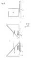
- the substrate table WTis at a measurement station where alignment and/or level measurement take place.
- the substrate tableis provided with a reference F 1 , sometimes referred to as a fiducial, which can comprise a plate etched through with a pattern corresponding to a standard alignment mark underneath which is a radiation sensor, also known as a transmission image sensor, responsive to radiation.
- the substrate table WTis moved to detect the reference F 1 using an alignment system within the measurement system 30 and then to detect the alignment marks on the substrate W thereby enabling the location (in directions x, y and R z ) of the substrate alignment marks to be found.
- the location of the alignment marksare measured and determined relative to the reference.
- Level measurement of the substratethen occurs at the measurement station.
- a leveling beam(projected from the measurement system 30 ) can be used that traverses a first grating prior to reflection by the substrate W.
- a second gratingis then placed in the path of the leveling beam after reflection by the substrate W.
- the extent to which the images of the first and second gratings coincideis measured by a level measurement sensor and is determined by the height and/or tilts of the substrate W (the z, R x and R y coordinates are thus determined).
- level measurement of substratesreference is made to European patent application EP 0502583.
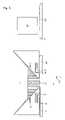
- substrate table WTis then moved to the separate exposure station where a liquid supply 18 is provided to supply liquid (e.g. water) to a space between the projection system PL and the substrate table WT to form a liquid reservoir 10 .
- liquide.g. water
- the reservoir 10forms a contactless seal to the substrate around the image field of the projection system PL so that liquid is confined to fill a space between the substrate surface and the final element of the projection system PL.
- a seal member 12positioned below and surrounding the final element of the projection system PL, borders the reservoir 10 and comprises the liquid supply 18 .
- the seal member 12extends a little above the final element of the projection system and has an inner periphery that at the upper end closely conforms to the step of the projection system or the final element thereof and may, e.g., be round. At the bottom, the inner periphery closely conforms to the shape of the image field, e.g., rectangular though this need not be the case. Liquid is brought into the space below the projection system and within the seal member 12 and the liquid level rises above the final element of the projection system PL so that a buffer of liquid is provided.
- a gas seal 16formed between the bottom of the seal member 12 and the surface of the substrate W, confines the liquid in the reservoir.
- the gas sealis formed by gas, e.g. air or synthetic air but in an embodiment, N 2 or another inert gas, provided under pressure via inlet 15 to the gap between seal member 12 and the substrate W and extracted via first outlet 14 .
- An overpressure on the gas inlet 15 , vacuum level on the first outlet 14 and geometry of the gapare arranged so that there is a high-velocity gas flow inwards that confines the liquid.
- the liquid reservoir defined by inlet(s) IN and outlet(s) OUT as shown in FIGS. 4 and 5can be similarly applied.
- a measurement stationcan be provided as well as an exposure station comprising inlet(s) IN and outlet(s) OUT.
- the reference F 1is scanned in three dimensions through the aerial image of an alignment mark on the mask MA.
- the maximum signalis returned when the reference is aligned with the image of the mark on the mask in the plane of best focus.
- suitable position measurements devicescan be used such as an interferometer beam projected towards one or more sides of the substrate table WT.
- a particular point on the substrate tablecan be placed at the focal point of the projection system PL and exposure of a target portion C of the substrate W can take place.
- the liquid reservoirPrior to the substrate table WT leaving the exposure station, the liquid reservoir can be emptied, for example in the case shown in FIGS. 2 and 3 , by reducing the gas inlet pressure and allowing the liquid to be sucked out by the vacuum system or, for example in the case shown in FIGS. 4 and 5 , by discontinuing flow of liquid onto the substrate through inlet IN and allowing the liquid to be sucked out by outlet OUT.
- the position of the transmission image sensor described abovecan be sensed through the liquid, or alternatively not through the liquid and a correction applied.
- the substrate tablesare movable between an exposure station and a measurement station.
- off-axis measurementcan be used.
- the reference mark F 1can be aligned using another system near the projection system PL.
- a different reference and a different systemfor example one with an axis perpendicular to the projection axis of the projection system can be used. Further description of such off-axis measurement can be found in European patent application publication EP 0906590.
- liquid in liquid reservoir 10may not need to be completely removed and could just be refilled as necessary.
- Detection and measurement of an alignment marktakes place at the exposure station but with no liquid in reservoir 10 .
- the liquid reservoir 10is then filled up and exposure takes place.
- level measurementcan take place at the exposure station with no liquid in reservoir 10 .
- These measurementscan be either off-axis or on-axis.
Landscapes
- Physics & Mathematics (AREA)
- General Physics & Mathematics (AREA)
- Engineering & Computer Science (AREA)
- Multimedia (AREA)
- Health & Medical Sciences (AREA)
- Environmental & Geological Engineering (AREA)
- Epidemiology (AREA)
- Public Health (AREA)
- Exposure And Positioning Against Photoresist Photosensitive Materials (AREA)
- Exposure Of Semiconductors, Excluding Electron Or Ion Beam Exposure (AREA)
Abstract
Description
- A mask. The concept of a mask is well known in lithography, and it includes mask types such as binary, alternating phase-shift, and attenuated phase-shift, as well as various hybrid mask types. Placement of such a mask in the radiation beam causes selective transmission (in the case of a transmissive mask) or reflection (in the case of a reflective mask) of the radiation impinging on the mask, according to the pattern on the mask. In the case of a mask, the support structure will generally be a mask table, which ensures that the mask can be held at a desired position in the incoming radiation beam, and that it can be moved relative to the beam if so desired.
- A programmable mirror array. One example of such a device is a matrix-addressable surface having a viscoelastic control layer and a reflective surface. The basic principle behind such an apparatus is that (for example) addressed areas of the reflective surface reflect incident light as diffracted light, whereas unaddressed areas reflect incident light as undiffracted light. Using an appropriate filter, the said undiffracted light can be filtered out of the reflected beam, leaving only the diffracted light behind; in this manner, the beam becomes patterned according to the addressing pattern of the matrix-addressable surface. An alternative embodiment of a programmable mirror array employs a matrix arrangement of tiny mirrors, each of which can be individually tilted about an axis by applying a suitable localized electric field, or by employing piezoelectric actuation means. Once again, the mirrors are matrix-addressable, such that addressed mirrors will reflect an incoming radiation beam in a different direction to unaddressed mirrors; in this manner, the reflected beam is patterned according to the addressing pattern of the matrix-addressable mirrors. The required matrix addressing can be performed using suitable electronic means. In both of the situations described hereabove, the patterning device can comprise one or more programmable mirror arrays. More information on mirror arrays as here referred to can be gleaned, for example, from U.S. Pat. Nos. 5,296,891 and 5,523,193, and PCT patent applications WO 98/38597 and WO 98/33096, which are incorporated herein by reference. In the case of a programmable mirror array, the said support structure may be embodied as a frame or table, for example, which may be fixed or movable as required.
- A programmable LCD array. An example of such a construction is given in U.S. Pat. No. 5,229,872, which is incorporated herein by reference. As above, the support structure in this case may be embodied as a frame or table, for example, which may be fixed or movable as required.
where k is a pre-factor. The numerical aperture NA is n sin θ where n is the refractive index of the transmissive substance.
- a radiation system Ex, IL, for supplying a projection beam PB of radiation (e.g. UV radiation), which in this particular case also comprises a radiation source LA;
- a first object table (mask table) MT provided with a mask holder for holding a mask MA (e.g. a reticle), and connected to first positioning means for accurately positioning the mask with respect to item PL;
- a second object table (substrate table) WT provided with a substrate holder for holding a substrate W (e.g. a resist-coated silicon wafer), and connected to second positioning means for accurately positioning the substrate with respect to item PL;
- a projection system (“lens”) PL (e.g. a refractive lens system) for imaging an irradiated portion of the mask MA onto a target portion C (e.g. comprising one or more dies) of the substrate W.
Claims (38)
Priority Applications (5)
| Application Number | Priority Date | Filing Date | Title |
|---|---|---|---|
| US11/371,235US7482611B2 (en) | 2002-11-12 | 2006-03-09 | Lithographic apparatus and device manufacturing method |
| US12/318,036US7795603B2 (en) | 2002-11-12 | 2008-12-19 | Lithographic apparatus and device manufacturing method |
| US12/853,030US8344341B2 (en) | 2002-11-12 | 2010-08-09 | Lithographic apparatus and device manufacturing method |
| US13/692,865US9195153B2 (en) | 2002-11-12 | 2012-12-03 | Lithographic apparatus and device manufacturing method |
| US14/937,724US20160062248A1 (en) | 2002-11-12 | 2015-11-10 | Lithographic apparatus and device manufacturing method |
Applications Claiming Priority (6)
| Application Number | Priority Date | Filing Date | Title |
|---|---|---|---|
| EP02257822.3 | 2002-11-12 | ||
| EP02257822 | 2002-11-12 | ||
| EP03253692.2 | 2003-06-11 | ||
| EP03253692 | 2003-06-11 | ||
| US10/705,816US7193232B2 (en) | 2002-11-12 | 2003-11-12 | Lithographic apparatus and device manufacturing method with substrate measurement not through liquid |
| US11/371,235US7482611B2 (en) | 2002-11-12 | 2006-03-09 | Lithographic apparatus and device manufacturing method |
Related Parent Applications (1)
| Application Number | Title | Priority Date | Filing Date |
|---|---|---|---|
| US10/705,816ContinuationUS7193232B2 (en) | 2002-11-12 | 2003-11-12 | Lithographic apparatus and device manufacturing method with substrate measurement not through liquid |
Related Child Applications (1)
| Application Number | Title | Priority Date | Filing Date |
|---|---|---|---|
| US12/318,036ContinuationUS7795603B2 (en) | 2002-11-12 | 2008-12-19 | Lithographic apparatus and device manufacturing method |
Publications (2)
| Publication Number | Publication Date |
|---|---|
| US20070040133A1 US20070040133A1 (en) | 2007-02-22 |
| US7482611B2true US7482611B2 (en) | 2009-01-27 |
Family
ID=32715008
Family Applications (6)
| Application Number | Title | Priority Date | Filing Date |
|---|---|---|---|
| US10/705,816Expired - LifetimeUS7193232B2 (en) | 2002-11-12 | 2003-11-12 | Lithographic apparatus and device manufacturing method with substrate measurement not through liquid |
| US11/371,235Expired - Fee RelatedUS7482611B2 (en) | 2002-11-12 | 2006-03-09 | Lithographic apparatus and device manufacturing method |
| US12/318,036Expired - Fee RelatedUS7795603B2 (en) | 2002-11-12 | 2008-12-19 | Lithographic apparatus and device manufacturing method |
| US12/853,030Expired - Fee RelatedUS8344341B2 (en) | 2002-11-12 | 2010-08-09 | Lithographic apparatus and device manufacturing method |
| US13/692,865Expired - Fee RelatedUS9195153B2 (en) | 2002-11-12 | 2012-12-03 | Lithographic apparatus and device manufacturing method |
| US14/937,724AbandonedUS20160062248A1 (en) | 2002-11-12 | 2015-11-10 | Lithographic apparatus and device manufacturing method |
Family Applications Before (1)
| Application Number | Title | Priority Date | Filing Date |
|---|---|---|---|
| US10/705,816Expired - LifetimeUS7193232B2 (en) | 2002-11-12 | 2003-11-12 | Lithographic apparatus and device manufacturing method with substrate measurement not through liquid |
Family Applications After (4)
| Application Number | Title | Priority Date | Filing Date |
|---|---|---|---|
| US12/318,036Expired - Fee RelatedUS7795603B2 (en) | 2002-11-12 | 2008-12-19 | Lithographic apparatus and device manufacturing method |
| US12/853,030Expired - Fee RelatedUS8344341B2 (en) | 2002-11-12 | 2010-08-09 | Lithographic apparatus and device manufacturing method |
| US13/692,865Expired - Fee RelatedUS9195153B2 (en) | 2002-11-12 | 2012-12-03 | Lithographic apparatus and device manufacturing method |
| US14/937,724AbandonedUS20160062248A1 (en) | 2002-11-12 | 2015-11-10 | Lithographic apparatus and device manufacturing method |
Country Status (6)
| Country | Link |
|---|---|
| US (6) | US7193232B2 (en) |
| JP (3) | JP4234567B2 (en) |
| KR (1) | KR100588123B1 (en) |
| CN (1) | CN100562805C (en) |
| SG (1) | SG121822A1 (en) |
| TW (1) | TWI240851B (en) |
Cited By (6)
| Publication number | Priority date | Publication date | Assignee | Title |
|---|---|---|---|---|
| US20060132740A1 (en)* | 2003-06-19 | 2006-06-22 | Nikon Corporation | Exposure apparatus, and device manufacturing method |
| US20060285093A1 (en)* | 2005-06-21 | 2006-12-21 | Canon Kabushiki Kaisha | Immersion exposure apparatus |
| US20070247602A1 (en)* | 2003-04-11 | 2007-10-25 | Nikon Corporation | Apparatus and method for maintaining immersion fluid in the gap under the projection lens during wafer exchange in an immersion lithography machine |
| US20070247607A1 (en)* | 2004-02-02 | 2007-10-25 | Nikon Corporation | Stage drive method and stage unit, exposure apparatus, and device manufacturing method |
| US20100097584A1 (en)* | 2006-12-13 | 2010-04-22 | Canon Kabushiki Kaisha | Exposure apparatus and device fabrication method |
| US7768625B2 (en) | 2005-06-02 | 2010-08-03 | Canon Kabushiki Kaisha | Photo detector unit and exposure apparatus having the same |
Families Citing this family (373)
| Publication number | Priority date | Publication date | Assignee | Title |
|---|---|---|---|---|
| US7234477B2 (en)* | 2000-06-30 | 2007-06-26 | Lam Research Corporation | Method and apparatus for drying semiconductor wafer surfaces using a plurality of inlets and outlets held in close proximity to the wafer surfaces |
| US7584761B1 (en)* | 2000-06-30 | 2009-09-08 | Lam Research Corporation | Wafer edge surface treatment with liquid meniscus |
| AU2003250898A1 (en)* | 2002-08-08 | 2004-03-11 | Carl Zeiss Smt Ag | Device for receiving an optical module in an imaging unit |
| US7383843B2 (en)* | 2002-09-30 | 2008-06-10 | Lam Research Corporation | Method and apparatus for processing wafer surfaces using thin, high velocity fluid layer |
| US7293571B2 (en) | 2002-09-30 | 2007-11-13 | Lam Research Corporation | Substrate proximity processing housing and insert for generating a fluid meniscus |
| US6988326B2 (en)* | 2002-09-30 | 2006-01-24 | Lam Research Corporation | Phobic barrier meniscus separation and containment |
| US7153400B2 (en)* | 2002-09-30 | 2006-12-26 | Lam Research Corporation | Apparatus and method for depositing and planarizing thin films of semiconductor wafers |
| US7513262B2 (en) | 2002-09-30 | 2009-04-07 | Lam Research Corporation | Substrate meniscus interface and methods for operation |
| US7997288B2 (en)* | 2002-09-30 | 2011-08-16 | Lam Research Corporation | Single phase proximity head having a controlled meniscus for treating a substrate |
| US7252097B2 (en)* | 2002-09-30 | 2007-08-07 | Lam Research Corporation | System and method for integrating in-situ metrology within a wafer process |
| US7198055B2 (en)* | 2002-09-30 | 2007-04-03 | Lam Research Corporation | Meniscus, vacuum, IPA vapor, drying manifold |
| US7614411B2 (en) | 2002-09-30 | 2009-11-10 | Lam Research Corporation | Controls of ambient environment during wafer drying using proximity head |
| US8236382B2 (en)* | 2002-09-30 | 2012-08-07 | Lam Research Corporation | Proximity substrate preparation sequence, and method, apparatus, and system for implementing the same |
| US6988327B2 (en) | 2002-09-30 | 2006-01-24 | Lam Research Corporation | Methods and systems for processing a substrate using a dynamic liquid meniscus |
| US7632376B1 (en) | 2002-09-30 | 2009-12-15 | Lam Research Corporation | Method and apparatus for atomic layer deposition (ALD) in a proximity system |
| US7389783B2 (en)* | 2002-09-30 | 2008-06-24 | Lam Research Corporation | Proximity meniscus manifold |
| US7045018B2 (en)* | 2002-09-30 | 2006-05-16 | Lam Research Corporation | Substrate brush scrubbing and proximity cleaning-drying sequence using compatible chemistries, and method, apparatus, and system for implementing the same |
| US7367345B1 (en) | 2002-09-30 | 2008-05-06 | Lam Research Corporation | Apparatus and method for providing a confined liquid for immersion lithography |
| KR100585476B1 (en)* | 2002-11-12 | 2006-06-07 | 에이에스엠엘 네델란즈 비.브이. | Lithographic Apparatus and Device Manufacturing Method |
| DE60335595D1 (en)* | 2002-11-12 | 2011-02-17 | Asml Netherlands Bv | Immersion lithographic apparatus and method of making a device |
| US9482966B2 (en) | 2002-11-12 | 2016-11-01 | Asml Netherlands B.V. | Lithographic apparatus and device manufacturing method |
| CN100568101C (en) | 2002-11-12 | 2009-12-09 | Asml荷兰有限公司 | Photolithography apparatus and device manufacturing method |
| US10503084B2 (en) | 2002-11-12 | 2019-12-10 | Asml Netherlands B.V. | Lithographic apparatus and device manufacturing method |
| SG121822A1 (en) | 2002-11-12 | 2006-05-26 | Asml Netherlands Bv | Lithographic apparatus and device manufacturing method |
| US7110081B2 (en) | 2002-11-12 | 2006-09-19 | Asml Netherlands B.V. | Lithographic apparatus and device manufacturing method |
| JP4352874B2 (en)* | 2002-12-10 | 2009-10-28 | 株式会社ニコン | Exposure apparatus and device manufacturing method |
| KR20120127755A (en)* | 2002-12-10 | 2012-11-23 | 가부시키가이샤 니콘 | Exposure apparatus and method for manufacturing device |
| EP1571694A4 (en)* | 2002-12-10 | 2008-10-15 | Nikon Corp | Exposure apparatus and method for manufacturing device |
| US7948604B2 (en)* | 2002-12-10 | 2011-05-24 | Nikon Corporation | Exposure apparatus and method for producing device |
| KR101101737B1 (en)* | 2002-12-10 | 2012-01-05 | 가부시키가이샤 니콘 | Exposure apparatus, exposure method and method for manufacturing device |
| WO2004053955A1 (en)* | 2002-12-10 | 2004-06-24 | Nikon Corporation | Exposure system and device producing method |
| US7242455B2 (en)* | 2002-12-10 | 2007-07-10 | Nikon Corporation | Exposure apparatus and method for producing device |
| US7514699B2 (en)* | 2002-12-19 | 2009-04-07 | Koninklijke Philips Electronics N.V. | Method and device for irradiating spots on a layer |
| DE10261775A1 (en) | 2002-12-20 | 2004-07-01 | Carl Zeiss Smt Ag | Device for the optical measurement of an imaging system |
| EP2466623B1 (en) | 2003-02-26 | 2015-04-22 | Nikon Corporation | Exposure apparatus, exposure method, and method for producing device |
| KR20050110033A (en)* | 2003-03-25 | 2005-11-22 | 가부시키가이샤 니콘 | Exposure system and device production method |
| EP1612850B1 (en)* | 2003-04-07 | 2009-03-25 | Nikon Corporation | Exposure apparatus and method for manufacturing a device |
| WO2004093159A2 (en)* | 2003-04-09 | 2004-10-28 | Nikon Corporation | Immersion lithography fluid control system |
| WO2004090633A2 (en)* | 2003-04-10 | 2004-10-21 | Nikon Corporation | An electro-osmotic element for an immersion lithography apparatus |
| EP3062152B1 (en)* | 2003-04-10 | 2017-12-20 | Nikon Corporation | Environmental system including vaccum scavenge for an immersion lithography apparatus |
| EP3352010A1 (en)* | 2003-04-10 | 2018-07-25 | Nikon Corporation | Run-off path to collect liquid for an immersion lithography apparatus |
| EP2950147B1 (en) | 2003-04-10 | 2017-04-26 | Nikon Corporation | Environmental system including vaccum scavenge for an immersion lithography apparatus |
| CN101825847B (en) | 2003-04-11 | 2013-10-16 | 株式会社尼康 | Cleanup method for optics in immersion lithography |
| JP4582089B2 (en) | 2003-04-11 | 2010-11-17 | 株式会社ニコン | Liquid jet recovery system for immersion lithography |
| SG194246A1 (en) | 2003-04-17 | 2013-11-29 | Nikon Corp | Optical arrangement of autofocus elements for use with immersion lithography |
| TWI295414B (en) | 2003-05-13 | 2008-04-01 | Asml Netherlands Bv | Lithographic apparatus and device manufacturing method |
| KR20060009356A (en)* | 2003-05-15 | 2006-01-31 | 가부시키가이샤 니콘 | Exposure apparatus and device manufacturing method |
| TWI421906B (en)* | 2003-05-23 | 2014-01-01 | 尼康股份有限公司 | An exposure method, an exposure apparatus, and an element manufacturing method |
| TW201806001A (en) | 2003-05-23 | 2018-02-16 | 尼康股份有限公司 | Exposure device and device manufacturing method |
| KR101548832B1 (en)* | 2003-05-28 | 2015-09-01 | 가부시키가이샤 니콘 | Exposure method, exposure device, and device manufacturing method |
| TWI442694B (en)* | 2003-05-30 | 2014-06-21 | Asml Netherlands Bv | Lithographic apparatus and device manufacturing method |
| US7213963B2 (en) | 2003-06-09 | 2007-05-08 | Asml Netherlands B.V. | Lithographic apparatus and device manufacturing method |
| EP2261741A3 (en) | 2003-06-11 | 2011-05-25 | ASML Netherlands B.V. | Lithographic apparatus and device manufacturing method |
| US7317504B2 (en)* | 2004-04-08 | 2008-01-08 | Asml Netherlands B.V. | Lithographic apparatus and device manufacturing method |
| KR101242815B1 (en)* | 2003-06-13 | 2013-03-12 | 가부시키가이샤 니콘 | Exposure method, substrate stage, exposure apparatus and method for manufacturing device |
| US6867844B2 (en)* | 2003-06-19 | 2005-03-15 | Asml Holding N.V. | Immersion photolithography system and method using microchannel nozzles |
| US7675000B2 (en)* | 2003-06-24 | 2010-03-09 | Lam Research Corporation | System method and apparatus for dry-in, dry-out, low defect laser dicing using proximity technology |
| US6809794B1 (en)* | 2003-06-27 | 2004-10-26 | Asml Holding N.V. | Immersion photolithography system and method using inverted wafer-projection optics interface |
| EP1494075B1 (en)* | 2003-06-30 | 2008-06-25 | ASML Netherlands B.V. | Lithographic projection apparatus and device manufacturing method |
| KR20060027832A (en)* | 2003-07-01 | 2006-03-28 | 가부시키가이샤 니콘 | Method of Using Isotopically Specified Fluids as Optical Elements |
| EP3179309A1 (en)* | 2003-07-08 | 2017-06-14 | Nikon Corporation | Wafer table for immersion lithography |
| WO2005006418A1 (en)* | 2003-07-09 | 2005-01-20 | Nikon Corporation | Exposure apparatus and method for manufacturing device |
| EP1643543B1 (en)* | 2003-07-09 | 2010-11-24 | Nikon Corporation | Exposure apparatus and method for manufacturing device |
| WO2005006415A1 (en)* | 2003-07-09 | 2005-01-20 | Nikon Corporation | Exposure apparatus and method for manufacturing device |
| SG109000A1 (en)* | 2003-07-16 | 2005-02-28 | Asml Netherlands Bv | Lithographic apparatus and device manufacturing method |
| EP1500982A1 (en)* | 2003-07-24 | 2005-01-26 | ASML Netherlands B.V. | Lithographic apparatus and device manufacturing method |
| WO2005010960A1 (en)* | 2003-07-25 | 2005-02-03 | Nikon Corporation | Inspection method and inspection device for projection optical system, and production method for projection optical system |
| KR101641011B1 (en)* | 2003-07-28 | 2016-07-19 | 가부시키가이샤 니콘 | Exposure apparatus, device producing method, and exposure apparatus controlling method |
| EP1503244A1 (en) | 2003-07-28 | 2005-02-02 | ASML Netherlands B.V. | Lithographic projection apparatus and device manufacturing method |
| US7175968B2 (en)* | 2003-07-28 | 2007-02-13 | Asml Netherlands B.V. | Lithographic apparatus, device manufacturing method and a substrate |
| US7326522B2 (en) | 2004-02-11 | 2008-02-05 | Asml Netherlands B.V. | Device manufacturing method and a substrate |
| US7779781B2 (en) | 2003-07-31 | 2010-08-24 | Asml Netherlands B.V. | Lithographic apparatus and device manufacturing method |
| KR101475995B1 (en)* | 2003-08-21 | 2014-12-23 | 가부시키가이샤 니콘 | Exposure apparatus, exposure method, and device producing method |
| JP4474652B2 (en) | 2003-08-26 | 2010-06-09 | 株式会社ニコン | Optical element and exposure apparatus |
| US8149381B2 (en)* | 2003-08-26 | 2012-04-03 | Nikon Corporation | Optical element and exposure apparatus |
| KR101477850B1 (en)* | 2003-08-29 | 2014-12-30 | 가부시키가이샤 니콘 | Liquid recovery apparatus, exposure apparatus, exposure method, and device production method |
| EP2261740B1 (en) | 2003-08-29 | 2014-07-09 | ASML Netherlands BV | Lithographic apparatus |
| KR101380989B1 (en)* | 2003-08-29 | 2014-04-04 | 가부시키가이샤 니콘 | Exposure apparatus and device producing method |
| TWI245163B (en) | 2003-08-29 | 2005-12-11 | Asml Netherlands Bv | Lithographic apparatus and device manufacturing method |
| TWI263859B (en) | 2003-08-29 | 2006-10-11 | Asml Netherlands Bv | Lithographic apparatus and device manufacturing method |
| EP3223053A1 (en)* | 2003-09-03 | 2017-09-27 | Nikon Corporation | Apparatus and method for providing fluid for immersion lithography |
| JP4444920B2 (en)* | 2003-09-19 | 2010-03-31 | 株式会社ニコン | Exposure apparatus and device manufacturing method |
| JP5136566B2 (en)* | 2003-09-29 | 2013-02-06 | 株式会社ニコン | Exposure apparatus, exposure method, and device manufacturing method |
| EP2837969B1 (en) | 2003-09-29 | 2016-04-20 | Nikon Corporation | Exposure apparatus, exposure method, and method for producing device |
| EP1519231B1 (en)* | 2003-09-29 | 2005-12-21 | ASML Netherlands B.V. | Lithographic apparatus and device manufacturing method |
| US7158211B2 (en)* | 2003-09-29 | 2007-01-02 | Asml Netherlands B.V. | Lithographic apparatus and device manufacturing method |
| KR20060126949A (en) | 2003-10-08 | 2006-12-11 | 가부시키가이샤 니콘 | Substrate conveyance apparatus and substrate conveyance method, exposure apparatus, exposure method, and device manufacturing method |
| KR101203028B1 (en) | 2003-10-08 | 2012-11-21 | 가부시키가이샤 자오 니콘 | Substrate carrying apparatus, substrate carrying method, exposure apparatus, exposure method, and method for producing device |
| JP2005136364A (en)* | 2003-10-08 | 2005-05-26 | Zao Nikon Co Ltd | Substrate transport apparatus, exposure apparatus, and device manufacturing method |
| TWI553701B (en) | 2003-10-09 | 2016-10-11 | 尼康股份有限公司 | Exposure apparatus and exposure method, component manufacturing method |
| EP1524558A1 (en) | 2003-10-15 | 2005-04-20 | ASML Netherlands B.V. | Lithographic apparatus and device manufacturing method |
| EP1524557A1 (en) | 2003-10-15 | 2005-04-20 | ASML Netherlands B.V. | Lithographic apparatus and device manufacturing method |
| US7352433B2 (en) | 2003-10-28 | 2008-04-01 | Asml Netherlands B.V. | Lithographic apparatus and device manufacturing method |
| US7411653B2 (en)* | 2003-10-28 | 2008-08-12 | Asml Netherlands B.V. | Lithographic apparatus |
| CN100461336C (en)* | 2003-10-31 | 2009-02-11 | 株式会社尼康 | Exposure apparatus and device manufacturing method |
| US7528929B2 (en) | 2003-11-14 | 2009-05-05 | Asml Netherlands B.V. | Lithographic apparatus and device manufacturing method |
| US7545481B2 (en) | 2003-11-24 | 2009-06-09 | Asml Netherlands B.V. | Lithographic apparatus and device manufacturing method |
| KR101394764B1 (en) | 2003-12-03 | 2014-05-27 | 가부시키가이샤 니콘 | Exposure apparatus, exposure method, device producing method, and optical component |
| JPWO2005057635A1 (en)* | 2003-12-15 | 2007-07-05 | 株式会社ニコン | Projection exposure apparatus, stage apparatus, and exposure method |
| JP4720506B2 (en) | 2003-12-15 | 2011-07-13 | 株式会社ニコン | Stage apparatus, exposure apparatus, and exposure method |
| US20070081133A1 (en)* | 2004-12-14 | 2007-04-12 | Niikon Corporation | Projection exposure apparatus and stage unit, and exposure method |
| JP4308638B2 (en)* | 2003-12-17 | 2009-08-05 | パナソニック株式会社 | Pattern formation method |
| US7589818B2 (en)* | 2003-12-23 | 2009-09-15 | Asml Netherlands B.V. | Lithographic apparatus, alignment apparatus, device manufacturing method, and a method of converting an apparatus |
| US7394521B2 (en)* | 2003-12-23 | 2008-07-01 | Asml Netherlands B.V. | Lithographic apparatus and device manufacturing method |
| EP1703548B1 (en)* | 2004-01-05 | 2010-05-12 | Nikon Corporation | Exposure apparatus, exposure method, and device producing method |
| DE602005019689D1 (en)* | 2004-01-20 | 2010-04-15 | Zeiss Carl Smt Ag | EXPOSURE DEVICE AND MEASURING DEVICE FOR A PROJECTION SECTOR |
| WO2005076321A1 (en) | 2004-02-03 | 2005-08-18 | Nikon Corporation | Exposure apparatus and method of producing device |
| KR101309428B1 (en)* | 2004-02-04 | 2013-09-23 | 가부시키가이샤 니콘 | Exposure apparatus, exposure method, and device producing method |
| US7050146B2 (en) | 2004-02-09 | 2006-05-23 | Asml Netherlands B.V. | Lithographic apparatus and device manufacturing method |
| US20070030467A1 (en)* | 2004-02-19 | 2007-02-08 | Nikon Corporation | Exposure apparatus, exposure method, and device fabricating method |
| US20080151200A1 (en)* | 2004-02-19 | 2008-06-26 | Nikon Corporation | Exposure Apparatus and Device Manufacturing Method |
| CN100524616C (en)* | 2004-02-19 | 2009-08-05 | 株式会社尼康 | Exposure apparatus, exposure method, and device fabricating method |
| KR101851511B1 (en) | 2004-03-25 | 2018-04-23 | 가부시키가이샤 니콘 | Exposure apparatus and method for manufacturing device |
| US8062471B2 (en)* | 2004-03-31 | 2011-11-22 | Lam Research Corporation | Proximity head heating method and apparatus |
| US7034917B2 (en)* | 2004-04-01 | 2006-04-25 | Asml Netherlands B.V. | Lithographic apparatus, device manufacturing method and device manufactured thereby |
| US7898642B2 (en) | 2004-04-14 | 2011-03-01 | Asml Netherlands B.V. | Lithographic apparatus and device manufacturing method |
| WO2005104195A1 (en) | 2004-04-19 | 2005-11-03 | Nikon Corporation | Exposure apparatus and device producing method |
| US7379159B2 (en) | 2004-05-03 | 2008-05-27 | Asml Netherlands B.V. | Lithographic apparatus and device manufacturing method |
| US8054448B2 (en)* | 2004-05-04 | 2011-11-08 | Nikon Corporation | Apparatus and method for providing fluid for immersion lithography |
| US7616383B2 (en)* | 2004-05-18 | 2009-11-10 | Asml Netherlands B.V. | Lithographic apparatus and device manufacturing method |
| US7486381B2 (en)* | 2004-05-21 | 2009-02-03 | Asml Netherlands B.V. | Lithographic apparatus and device manufacturing method |
| CN100594430C (en) | 2004-06-04 | 2010-03-17 | 卡尔蔡司Smt股份公司 | System for measuring image quality of optical imaging system |
| US20070103661A1 (en)* | 2004-06-04 | 2007-05-10 | Nikon Corporation | Exposure apparatus, exposure method, and method for producing device |
| WO2005119742A1 (en)* | 2004-06-04 | 2005-12-15 | Nikon Corporation | Exposure apparatus, exposure method, and device producing method |
| EP3203498A1 (en) | 2004-06-09 | 2017-08-09 | Nikon Corporation | Exposure apparatus and device manufacturing method |
| US8373843B2 (en)* | 2004-06-10 | 2013-02-12 | Nikon Corporation | Exposure apparatus, exposure method, and method for producing device |
| US8508713B2 (en)* | 2004-06-10 | 2013-08-13 | Nikon Corporation | Exposure apparatus, exposure method, and method for producing device |
| EP3067749B1 (en)* | 2004-06-10 | 2017-10-18 | Nikon Corporation | Exposure apparatus, exposure method, and method for producing device |
| KR101178755B1 (en)* | 2004-06-10 | 2012-08-31 | 가부시키가이샤 니콘 엔지니어링 | Exposure equipment, exposure method and device manufacturing method |
| US8717533B2 (en)* | 2004-06-10 | 2014-05-06 | Nikon Corporation | Exposure apparatus, exposure method, and method for producing device |
| US7481867B2 (en) | 2004-06-16 | 2009-01-27 | Edwards Limited | Vacuum system for immersion photolithography |
| KR101330922B1 (en)* | 2004-06-21 | 2013-11-18 | 가부시키가이샤 니콘 | Exposure equipment and device manufacturing method |
| US20060001851A1 (en)* | 2004-07-01 | 2006-01-05 | Grant Robert B | Immersion photolithography system |
| US7463330B2 (en) | 2004-07-07 | 2008-12-09 | Asml Netherlands B.V. | Lithographic apparatus and device manufacturing method |
| JP4894515B2 (en) | 2004-07-12 | 2012-03-14 | 株式会社ニコン | Exposure apparatus, device manufacturing method, and liquid detection method |
| US7161663B2 (en)* | 2004-07-22 | 2007-01-09 | Asml Netherlands B.V. | Lithographic apparatus |
| US8169591B2 (en)* | 2004-08-03 | 2012-05-01 | Nikon Corporation | Exposure apparatus, exposure method, and method for producing device |
| US7304715B2 (en)* | 2004-08-13 | 2007-12-04 | Asml Netherlands B.V. | Lithographic apparatus and device manufacturing method |
| KR20070048164A (en)* | 2004-08-18 | 2007-05-08 | 가부시키가이샤 니콘 | Exposure apparatus and device manufacturing method |
| US7701550B2 (en)* | 2004-08-19 | 2010-04-20 | Asml Netherlands B.V. | Lithographic apparatus and device manufacturing method |
| US20060044533A1 (en)* | 2004-08-27 | 2006-03-02 | Asmlholding N.V. | System and method for reducing disturbances caused by movement in an immersion lithography system |
| CN100539019C (en)* | 2004-09-17 | 2009-09-09 | 株式会社尼康 | Exposure apparatus, exposure method, and device manufacturing method |
| US7133114B2 (en)* | 2004-09-20 | 2006-11-07 | Asml Netherlands B.V. | Lithographic apparatus and device manufacturing method |
| US7522261B2 (en) | 2004-09-24 | 2009-04-21 | Asml Netherlands B.V. | Lithographic apparatus and device manufacturing method |
| US7355674B2 (en) | 2004-09-28 | 2008-04-08 | Asml Netherlands B.V. | Lithographic apparatus, device manufacturing method and computer program product |
| US7894040B2 (en)* | 2004-10-05 | 2011-02-22 | Asml Netherlands B.V. | Lithographic apparatus and device manufacturing method |
| US7209213B2 (en)* | 2004-10-07 | 2007-04-24 | Asml Netherlands B.V. | Lithographic apparatus and device manufacturing method |
| WO2006041083A1 (en)* | 2004-10-13 | 2006-04-20 | Nikon Corporation | Exposure apparatus, exposure method and device manufacturing method |
| KR101364347B1 (en)* | 2004-10-15 | 2014-02-18 | 가부시키가이샤 니콘 | Exposure apparatus and device manufacturing method |
| US7119876B2 (en)* | 2004-10-18 | 2006-10-10 | Asml Netherlands B.V. | Lithographic apparatus and device manufacturing method |
| US7379155B2 (en)* | 2004-10-18 | 2008-05-27 | Asml Netherlands B.V. | Lithographic apparatus and device manufacturing method |
| US7414699B2 (en)* | 2004-11-12 | 2008-08-19 | Asml Netherlands B.V. | Lithographic apparatus and device manufacturing method |
| US7423720B2 (en) | 2004-11-12 | 2008-09-09 | Asml Netherlands B.V. | Lithographic apparatus and device manufacturing method |
| US7583357B2 (en) | 2004-11-12 | 2009-09-01 | Asml Netherlands B.V. | Lithographic apparatus and device manufacturing method |
| US7251013B2 (en) | 2004-11-12 | 2007-07-31 | Asml Netherlands B.V. | Lithographic apparatus and device manufacturing method |
| US7411657B2 (en)* | 2004-11-17 | 2008-08-12 | Asml Netherlands B.V. | Lithographic apparatus and device manufacturing method |
| US7362412B2 (en)* | 2004-11-18 | 2008-04-22 | International Business Machines Corporation | Method and apparatus for cleaning a semiconductor substrate in an immersion lithography system |
| TWI588872B (en)* | 2004-11-18 | 2017-06-21 | 尼康股份有限公司 | Position measurement method, position control method, measurement method, loading method, exposure method and exposure apparatus, and device manufacturing method |
| US7230681B2 (en)* | 2004-11-18 | 2007-06-12 | International Business Machines Corporation | Method and apparatus for immersion lithography |
| KR101166008B1 (en)* | 2004-11-19 | 2012-07-18 | 가부시키가이샤 니콘 | Maintenance method, exposure method, exposure apparatus, and device producing method |
| US7145630B2 (en)* | 2004-11-23 | 2006-12-05 | Asml Netherlands B.V. | Lithographic apparatus and device manufacturing method |
| US7161654B2 (en)* | 2004-12-02 | 2007-01-09 | Asml Netherlands B.V. | Lithographic apparatus and device manufacturing method |
| US7256121B2 (en)* | 2004-12-02 | 2007-08-14 | Texas Instruments Incorporated | Contact resistance reduction by new barrier stack process |
| US7446850B2 (en)* | 2004-12-03 | 2008-11-04 | Asml Netherlands B.V. | Lithographic apparatus and device manufacturing method |
| US7196770B2 (en)* | 2004-12-07 | 2007-03-27 | Asml Netherlands B.V. | Prewetting of substrate before immersion exposure |
| US7248334B2 (en)* | 2004-12-07 | 2007-07-24 | Asml Netherlands B.V. | Sensor shield |
| US7397533B2 (en)* | 2004-12-07 | 2008-07-08 | Asml Netherlands B.V. | Lithographic apparatus and device manufacturing method |
| US7365827B2 (en) | 2004-12-08 | 2008-04-29 | Asml Netherlands B.V. | Lithographic apparatus and device manufacturing method |
| US7352440B2 (en)* | 2004-12-10 | 2008-04-01 | Asml Netherlands B.V. | Substrate placement in immersion lithography |
| US7403261B2 (en)* | 2004-12-15 | 2008-07-22 | Asml Netherlands B.V. | Lithographic apparatus and device manufacturing method |
| US7880860B2 (en)* | 2004-12-20 | 2011-02-01 | Asml Netherlands B.V. | Lithographic apparatus and device manufacturing method |
| US7528931B2 (en) | 2004-12-20 | 2009-05-05 | Asml Netherlands B.V. | Lithographic apparatus and device manufacturing method |
| US7491661B2 (en)* | 2004-12-28 | 2009-02-17 | Asml Netherlands B.V. | Device manufacturing method, top coat material and substrate |
| US7405805B2 (en) | 2004-12-28 | 2008-07-29 | Asml Netherlands B.V. | Lithographic apparatus and device manufacturing method |
| US20060147821A1 (en) | 2004-12-30 | 2006-07-06 | Asml Netherlands B.V. | Lithographic apparatus and device manufacturing method |
| US7450217B2 (en)* | 2005-01-12 | 2008-11-11 | Asml Netherlands B.V. | Exposure apparatus, coatings for exposure apparatus, lithographic apparatus, device manufacturing method, and device manufactured thereby |
| DE602006012746D1 (en)* | 2005-01-14 | 2010-04-22 | Asml Netherlands Bv | Lithographic apparatus and manufacturing method |
| SG124351A1 (en)* | 2005-01-14 | 2006-08-30 | Asml Netherlands Bv | Lithographic apparatus and device manufacturing method |
| KR101513840B1 (en)* | 2005-01-31 | 2015-04-20 | 가부시키가이샤 니콘 | Exposure apparatus and method for manufacturing device |
| US8692973B2 (en)* | 2005-01-31 | 2014-04-08 | Nikon Corporation | Exposure apparatus and method for producing device |
| CN102360170B (en)* | 2005-02-10 | 2014-03-12 | Asml荷兰有限公司 | Immersion liquid, exposure apparatus, and exposure process |
| US20070258068A1 (en)* | 2005-02-17 | 2007-11-08 | Hiroto Horikawa | Exposure Apparatus, Exposure Method, and Device Fabricating Method |
| US7224431B2 (en)* | 2005-02-22 | 2007-05-29 | Asml Netherlands B.V. | Lithographic apparatus and device manufacturing method |
| US8018573B2 (en)* | 2005-02-22 | 2011-09-13 | Asml Netherlands B.V. | Lithographic apparatus and device manufacturing method |
| US7378025B2 (en) | 2005-02-22 | 2008-05-27 | Asml Netherlands B.V. | Fluid filtration method, fluid filtered thereby, lithographic apparatus and device manufacturing method |
| US7428038B2 (en) | 2005-02-28 | 2008-09-23 | Asml Netherlands B.V. | Lithographic apparatus, device manufacturing method and apparatus for de-gassing a liquid |
| US7282701B2 (en)* | 2005-02-28 | 2007-10-16 | Asml Netherlands B.V. | Sensor for use in a lithographic apparatus |
| US7324185B2 (en)* | 2005-03-04 | 2008-01-29 | Asml Netherlands B.V. | Lithographic apparatus and device manufacturing method |
| US7684010B2 (en)* | 2005-03-09 | 2010-03-23 | Asml Netherlands B.V. | Lithographic apparatus, device manufacturing method, seal structure, method of removing an object and a method of sealing |
| JP2006259143A (en)* | 2005-03-16 | 2006-09-28 | Fuji Xerox Co Ltd | Arranging device and method |
| JP2006261606A (en) | 2005-03-18 | 2006-09-28 | Canon Inc | Exposure apparatus, exposure method, and device manufacturing method |
| US7330238B2 (en)* | 2005-03-28 | 2008-02-12 | Asml Netherlands, B.V. | Lithographic apparatus, immersion projection apparatus and device manufacturing method |
| JP4605219B2 (en)* | 2005-03-30 | 2011-01-05 | 株式会社ニコン | Exposure condition determination method, exposure method and exposure apparatus, and device manufacturing method |
| US7411654B2 (en) | 2005-04-05 | 2008-08-12 | Asml Netherlands B.V. | Lithographic apparatus and device manufacturing method |
| USRE43576E1 (en) | 2005-04-08 | 2012-08-14 | Asml Netherlands B.V. | Dual stage lithographic apparatus and device manufacturing method |
| US7291850B2 (en)* | 2005-04-08 | 2007-11-06 | Asml Netherlands B.V. | Lithographic apparatus and device manufacturing method |
| US20060232753A1 (en)* | 2005-04-19 | 2006-10-19 | Asml Holding N.V. | Liquid immersion lithography system with tilted liquid flow |
| US7433016B2 (en) | 2005-05-03 | 2008-10-07 | Asml Netherlands B.V. | Lithographic apparatus and device manufacturing method |
| US8248577B2 (en)* | 2005-05-03 | 2012-08-21 | Asml Netherlands B.V. | Lithographic apparatus and device manufacturing method |
| US7317507B2 (en)* | 2005-05-03 | 2008-01-08 | Asml Netherlands B.V. | Lithographic apparatus and device manufacturing method |
| US7652746B2 (en)* | 2005-06-21 | 2010-01-26 | Asml Netherlands B.V. | Lithographic apparatus and device manufacturing method |
| US7751027B2 (en)* | 2005-06-21 | 2010-07-06 | Asml Netherlands B.V. | Lithographic apparatus and device manufacturing method |
| US7834974B2 (en) | 2005-06-28 | 2010-11-16 | Asml Netherlands B.V. | Lithographic apparatus and device manufacturing method |
| US7474379B2 (en) | 2005-06-28 | 2009-01-06 | Asml Netherlands B.V. | Lithographic apparatus and device manufacturing method |
| US7468779B2 (en)* | 2005-06-28 | 2008-12-23 | Asml Netherlands B.V. | Lithographic apparatus and device manufacturing method |
| US7535644B2 (en)* | 2005-08-12 | 2009-05-19 | Asml Netherlands B.V. | Lens element, lithographic apparatus, device manufacturing method, and device manufactured thereby |
| US8054445B2 (en)* | 2005-08-16 | 2011-11-08 | Asml Netherlands B.V. | Lithographic apparatus and device manufacturing method |
| TWI345685B (en)* | 2005-09-06 | 2011-07-21 | Asml Netherlands Bv | Lithographic method |
| US7357768B2 (en)* | 2005-09-22 | 2008-04-15 | William Marshall | Recliner exerciser |
| US7411658B2 (en)* | 2005-10-06 | 2008-08-12 | Asml Netherlands B.V. | Lithographic apparatus and device manufacturing method |
| JP4125315B2 (en)* | 2005-10-11 | 2008-07-30 | キヤノン株式会社 | Exposure apparatus and device manufacturing method |
| US7755742B2 (en)* | 2005-10-11 | 2010-07-13 | Asml Netherlands B.V. | Lithographic apparatus with mounted sensor |
| JPWO2007055237A1 (en)* | 2005-11-09 | 2009-04-30 | 株式会社ニコン | Exposure apparatus, exposure method, and device manufacturing method |
| US7656501B2 (en)* | 2005-11-16 | 2010-02-02 | Asml Netherlands B.V. | Lithographic apparatus |
| US7864292B2 (en) | 2005-11-16 | 2011-01-04 | Asml Netherlands B.V. | Lithographic apparatus and device manufacturing method |
| US7804577B2 (en) | 2005-11-16 | 2010-09-28 | Asml Netherlands B.V. | Lithographic apparatus |
| US7633073B2 (en) | 2005-11-23 | 2009-12-15 | Asml Netherlands B.V. | Lithographic apparatus and device manufacturing method |
| US7773195B2 (en)* | 2005-11-29 | 2010-08-10 | Asml Holding N.V. | System and method to increase surface tension and contact angle in immersion lithography |
| US20070124987A1 (en)* | 2005-12-05 | 2007-06-07 | Brown Jeffrey K | Electronic pest control apparatus |
| KR100768849B1 (en)* | 2005-12-06 | 2007-10-22 | 엘지전자 주식회사 | Power supply system and method for grid-connected fuel cell system |
| US7420194B2 (en)* | 2005-12-27 | 2008-09-02 | Asml Netherlands B.V. | Lithographic apparatus and substrate edge seal |
| US7839483B2 (en) | 2005-12-28 | 2010-11-23 | Asml Netherlands B.V. | Lithographic apparatus, device manufacturing method and a control system |
| US7649611B2 (en) | 2005-12-30 | 2010-01-19 | Asml Netherlands B.V. | Lithographic apparatus and device manufacturing method |
| US8045134B2 (en) | 2006-03-13 | 2011-10-25 | Asml Netherlands B.V. | Lithographic apparatus, control system and device manufacturing method |
| US7230676B1 (en)* | 2006-03-13 | 2007-06-12 | Asml Netherlands B.V. | Lithographic apparatus and device manufacturing method |
| US8027019B2 (en) | 2006-03-28 | 2011-09-27 | Asml Netherlands B.V. | Lithographic apparatus and device manufacturing method |
| JP2007266504A (en)* | 2006-03-29 | 2007-10-11 | Canon Inc | Exposure equipment |
| EP1843206B1 (en)* | 2006-04-06 | 2012-09-05 | ASML Netherlands B.V. | Lithographic apparatus and device manufacturing method |
| US9477158B2 (en)* | 2006-04-14 | 2016-10-25 | Asml Netherlands B.V. | Lithographic apparatus and device manufacturing method |
| US7701551B2 (en)* | 2006-04-14 | 2010-04-20 | Asml Netherlands B.V. | Lithographic apparatus and device manufacturing method |
| DE102006021797A1 (en) | 2006-05-09 | 2007-11-15 | Carl Zeiss Smt Ag | Optical imaging device with thermal damping |
| US8144305B2 (en)* | 2006-05-18 | 2012-03-27 | Asml Netherlands B.V. | Lithographic apparatus and device manufacturing method |
| US7969548B2 (en)* | 2006-05-22 | 2011-06-28 | Asml Netherlands B.V. | Lithographic apparatus and lithographic apparatus cleaning method |
| US7928366B2 (en)* | 2006-10-06 | 2011-04-19 | Lam Research Corporation | Methods of and apparatus for accessing a process chamber using a dual zone gas injector with improved optical access |
| US7656502B2 (en)* | 2006-06-22 | 2010-02-02 | Asml Netherlands B.V. | Lithographic apparatus and device manufacturing method |
| US7826030B2 (en) | 2006-09-07 | 2010-11-02 | Asml Netherlands B.V. | Lithographic apparatus and device manufacturing method |
| US8813764B2 (en) | 2009-05-29 | 2014-08-26 | Lam Research Corporation | Method and apparatus for physical confinement of a liquid meniscus over a semiconductor wafer |
| US8330936B2 (en) | 2006-09-20 | 2012-12-11 | Asml Netherlands B.V. | Lithographic apparatus and device manufacturing method |
| US8045135B2 (en)* | 2006-11-22 | 2011-10-25 | Asml Netherlands B.V. | Lithographic apparatus with a fluid combining unit and related device manufacturing method |
| US8634053B2 (en) | 2006-12-07 | 2014-01-21 | Asml Netherlands B.V. | Lithographic apparatus and device manufacturing method |
| US9632425B2 (en)* | 2006-12-07 | 2017-04-25 | Asml Holding N.V. | Lithographic apparatus, a dryer and a method of removing liquid from a surface |
| US7791709B2 (en)* | 2006-12-08 | 2010-09-07 | Asml Netherlands B.V. | Substrate support and lithographic process |
| US8634052B2 (en)* | 2006-12-13 | 2014-01-21 | Asml Netherlands B.V. | Lithographic apparatus and method involving a ring to cover a gap between a substrate and a substrate table |
| US8416383B2 (en)* | 2006-12-13 | 2013-04-09 | Asml Netherlands B.V. | Lithographic apparatus and method |
| US8146902B2 (en)* | 2006-12-21 | 2012-04-03 | Lam Research Corporation | Hybrid composite wafer carrier for wet clean equipment |
| US8654305B2 (en)* | 2007-02-15 | 2014-02-18 | Asml Holding N.V. | Systems and methods for insitu lens cleaning in immersion lithography |
| US8817226B2 (en) | 2007-02-15 | 2014-08-26 | Asml Holding N.V. | Systems and methods for insitu lens cleaning using ozone in immersion lithography |
| US8237911B2 (en) | 2007-03-15 | 2012-08-07 | Nikon Corporation | Apparatus and methods for keeping immersion fluid adjacent to an optical assembly during wafer exchange in an immersion lithography machine |
| US7975708B2 (en)* | 2007-03-30 | 2011-07-12 | Lam Research Corporation | Proximity head with angled vacuum conduit system, apparatus and method |
| US8464736B1 (en) | 2007-03-30 | 2013-06-18 | Lam Research Corporation | Reclaim chemistry |
| US7841352B2 (en)* | 2007-05-04 | 2010-11-30 | Asml Netherlands B.V. | Cleaning device, a lithographic apparatus and a lithographic apparatus cleaning method |
| US8011377B2 (en)* | 2007-05-04 | 2011-09-06 | Asml Netherlands B.V. | Cleaning device and a lithographic apparatus cleaning method |
| US8947629B2 (en)* | 2007-05-04 | 2015-02-03 | Asml Netherlands B.V. | Cleaning device, a lithographic apparatus and a lithographic apparatus cleaning method |
| US7866330B2 (en)* | 2007-05-04 | 2011-01-11 | Asml Netherlands B.V. | Cleaning device, a lithographic apparatus and a lithographic apparatus cleaning method |
| US8435593B2 (en) | 2007-05-22 | 2013-05-07 | Asml Netherlands B.V. | Method of inspecting a substrate and method of preparing a substrate for lithography |
| US8514365B2 (en)* | 2007-06-01 | 2013-08-20 | Asml Netherlands B.V. | Lithographic apparatus and device manufacturing method |
| US8141566B2 (en)* | 2007-06-19 | 2012-03-27 | Lam Research Corporation | System, method and apparatus for maintaining separation of liquids in a controlled meniscus |
| US20090025753A1 (en)* | 2007-07-24 | 2009-01-29 | Asml Netherlands B.V. | Lithographic Apparatus And Contamination Removal Or Prevention Method |
| US7916269B2 (en) | 2007-07-24 | 2011-03-29 | Asml Netherlands B.V. | Lithographic apparatus and contamination removal or prevention method |
| NL1035757A1 (en)* | 2007-08-02 | 2009-02-03 | Asml Netherlands Bv | Lithographic apparatus and device manufacturing method. |
| US7924404B2 (en)* | 2007-08-16 | 2011-04-12 | Asml Netherlands B.V. | Lithographic apparatus and device manufacturing method |
| US8681308B2 (en)* | 2007-09-13 | 2014-03-25 | Asml Netherlands B.V. | Lithographic apparatus and device manufacturing method |
| NL1035908A1 (en) | 2007-09-25 | 2009-03-26 | Asml Netherlands Bv | Lithographic apparatus and device manufacturing method. |
| SG151198A1 (en) | 2007-09-27 | 2009-04-30 | Asml Netherlands Bv | Methods relating to immersion lithography and an immersion lithographic apparatus |
| NL1036009A1 (en)* | 2007-10-05 | 2009-04-07 | Asml Netherlands Bv | An Immersion Lithography Apparatus. |
| NL1036069A1 (en)* | 2007-10-30 | 2009-05-07 | Asml Netherlands Bv | An Immersion Lithography Apparatus. |
| JP5017232B2 (en)* | 2007-10-31 | 2012-09-05 | エーエスエムエル ネザーランズ ビー.ブイ. | Cleaning apparatus and immersion lithography apparatus |
| JP2009117832A (en) | 2007-11-06 | 2009-05-28 | Asml Netherlands Bv | Method of preparing substrate for lithography, substrate, device manufacturing method, sealing coating applicator, and sealing coating measuring device |
| NL1036194A1 (en)* | 2007-12-03 | 2009-06-04 | Asml Netherlands Bv | Lithographic apparatus and device manufacturing method. |
| NL1036187A1 (en)* | 2007-12-03 | 2009-06-04 | Asml Netherlands Bv | Lithographic apparatus and device manufacturing method. |
| NL1036186A1 (en)* | 2007-12-03 | 2009-06-04 | Asml Netherlands Bv | Lithographic apparatus and device manufacturing method. |
| NL1036211A1 (en)* | 2007-12-03 | 2009-06-04 | Asml Netherlands Bv | Lithographic Apparatus and Device Manufacturing Method. |
| NL1036253A1 (en)* | 2007-12-10 | 2009-06-11 | Asml Netherlands Bv | Lithographic apparatus and device manufacturing method. |
| NL1036273A1 (en)* | 2007-12-18 | 2009-06-19 | Asml Netherlands Bv | Lithographic apparatus and method of cleaning a surface or an immersion lithographic apparatus. |
| NL1036306A1 (en) | 2007-12-20 | 2009-06-23 | Asml Netherlands Bv | Lithographic apparatus and in-line cleaning apparatus. |
| NL1036333A1 (en)* | 2008-01-02 | 2009-07-07 | Asml Netherlands Bv | Immersion lithography. |
| US8339572B2 (en) | 2008-01-25 | 2012-12-25 | Asml Netherlands B.V. | Lithographic apparatus and device manufacturing method |
| US8889042B2 (en)* | 2008-02-14 | 2014-11-18 | Asml Netherlands B.V. | Coatings |
| NL1036571A1 (en)* | 2008-03-07 | 2009-09-08 | Asml Netherlands Bv | Lithographic Apparatus and Methods. |
| NL1036631A1 (en)* | 2008-03-24 | 2009-09-25 | Asml Netherlands Bv | Immersion Lithographic Apparatus and Device Manufacturing Method. |
| KR101448152B1 (en)* | 2008-03-26 | 2014-10-07 | 삼성전자주식회사 | Distance measuring sensor having vertical photogate and three dimensional color image sensor having the same |
| NL1036715A1 (en)* | 2008-04-16 | 2009-10-19 | Asml Netherlands Bv | Lithographic apparatus. |
| NL1036709A1 (en) | 2008-04-24 | 2009-10-27 | Asml Netherlands Bv | Lithographic apparatus and a method of operating the apparatus. |
| NL1036766A1 (en)* | 2008-04-25 | 2009-10-27 | Asml Netherlands Bv | Methods related to immersion lithography and an immersion lithographic apparatus. |
| NL1036835A1 (en)* | 2008-05-08 | 2009-11-11 | Asml Netherlands Bv | Lithographic Apparatus and Method. |
| EP2131241B1 (en)* | 2008-05-08 | 2019-07-31 | ASML Netherlands B.V. | Fluid handling structure, lithographic apparatus and device manufacturing method |
| ATE548679T1 (en) | 2008-05-08 | 2012-03-15 | Asml Netherlands Bv | LITHOGRAPHIC IMMERSION APPARATUS, DRYING APPARATUS, IMMERSION METROLOGY APPARATUS AND METHOD FOR PRODUCING A DEVICE |
| US8421993B2 (en) | 2008-05-08 | 2013-04-16 | Asml Netherlands B.V. | Fluid handling structure, lithographic apparatus and device manufacturing method |
| US9176393B2 (en) | 2008-05-28 | 2015-11-03 | Asml Netherlands B.V. | Lithographic apparatus and a method of operating the apparatus |
| NL1036924A1 (en)* | 2008-06-02 | 2009-12-03 | Asml Netherlands Bv | Substrate table, lithographic apparatus and device manufacturing method. |
| EP2131242A1 (en) | 2008-06-02 | 2009-12-09 | ASML Netherlands B.V. | Substrate table, lithographic apparatus and device manufacturing method |
| NL2002964A1 (en)* | 2008-06-16 | 2009-12-17 | Asml Netherlands Bv | Lithographic Apparatus, a Metrology Apparatus and a Method of Using the Apparatus. |
| EP2136250A1 (en) | 2008-06-18 | 2009-12-23 | ASML Netherlands B.V. | Lithographic apparatus and method |
| NL2002983A1 (en)* | 2008-06-26 | 2009-12-29 | Asml Netherlands Bv | A lithographic apparatus and a method of operating the lithographic apparatus. |
| JP4922359B2 (en) | 2008-07-25 | 2012-04-25 | エーエスエムエル ネザーランズ ビー.ブイ. | Fluid handling structure, lithographic apparatus, and device manufacturing method |
| NL2003226A (en)* | 2008-08-19 | 2010-03-09 | Asml Netherlands Bv | Lithographic apparatus, drying device, metrology apparatus and device manufacturing method. |
| NL2003341A (en)* | 2008-08-22 | 2010-03-10 | Asml Netherlands Bv | Lithographic apparatus and device manufacturing method. |
| SG159467A1 (en) | 2008-09-02 | 2010-03-30 | Asml Netherlands Bv | Fluid handling structure, lithographic apparatus and device manufacturing method |
| NL2003363A (en) | 2008-09-10 | 2010-03-15 | Asml Netherlands Bv | Lithographic apparatus, method of manufacturing an article for a lithographic apparatus and device manufacturing method. |
| NL2003392A (en) | 2008-09-17 | 2010-03-18 | Asml Netherlands Bv | Lithographic apparatus and a method of operating the apparatus. |
| NL2003362A (en)* | 2008-10-16 | 2010-04-19 | Asml Netherlands Bv | Lithographic apparatus and device manufacturing method. |
| NL2003421A (en)* | 2008-10-21 | 2010-04-22 | Asml Netherlands Bv | Lithographic apparatus and a method of removing contamination. |
| NL2003575A (en) | 2008-10-29 | 2010-05-03 | Asml Netherlands Bv | Lithographic apparatus and device manufacturing method. |
| JP5645836B2 (en)* | 2008-11-03 | 2014-12-24 | イエダ・リサーチ・アンド・デベロツプメント・カンパニー・リミテツド | Magnetic patterning method and system |
| NL2003638A (en)* | 2008-12-03 | 2010-06-07 | Asml Netherlands Bv | Lithographic apparatus and device manufacturing method. |
| NL2003758A (en)* | 2008-12-04 | 2010-06-07 | Asml Netherlands Bv | A member with a cleaning surface and a method of removing contamination. |
| JP5199982B2 (en) | 2008-12-08 | 2013-05-15 | エーエスエムエル ネザーランズ ビー.ブイ. | Lithographic apparatus |
| EP2196857A3 (en) | 2008-12-09 | 2010-07-21 | ASML Netherlands BV | Lithographic apparatus and device manufacturing method |
| JP5001343B2 (en) | 2008-12-11 | 2012-08-15 | エーエスエムエル ネザーランズ ビー.ブイ. | Fluid extraction system, immersion lithographic apparatus, and method for reducing pressure fluctuations of an immersion liquid used in an immersion lithographic apparatus |
| EP2199858A1 (en)* | 2008-12-18 | 2010-06-23 | ASML Netherlands BV | Lithographic apparatus and method of irradiating at least two target portions |
| NL2003820A (en)* | 2008-12-22 | 2010-06-23 | Asml Netherlands Bv | Fluid handling structure, table, lithographic apparatus, immersion lithographic apparatus, and device manufacturing methods. |
| NL2004162A (en)* | 2009-02-17 | 2010-08-18 | Asml Netherlands Bv | A fluid supply system, a lithographic apparatus, a method of varying fluid flow rate and a device manufacturing method. |
| EP2221669A3 (en) | 2009-02-19 | 2011-02-09 | ASML Netherlands B.V. | A lithographic apparatus, a method of controlling the apparatus and a device manufacturing method |
| NL2004102A (en)* | 2009-02-25 | 2010-08-26 | Asml Holding Nv | A fluid handling device, an immersion lithographic apparatus and a device manufacturing method. |
| NL2004305A (en) | 2009-03-13 | 2010-09-14 | Asml Netherlands Bv | Substrate table, immersion lithographic apparatus and device manufacturing method. |
| NL2004362A (en)* | 2009-04-10 | 2010-10-12 | Asml Netherlands Bv | A fluid handling device, an immersion lithographic apparatus and a device manufacturing method. |
| JP2010251745A (en)* | 2009-04-10 | 2010-11-04 | Asml Netherlands Bv | Immersion lithography device and device manufacturing method |
| NL2004363A (en)* | 2009-04-22 | 2010-10-26 | Asml Netherlands Bv | Lithographic apparatus and a method of operating the apparatus. |
| NL2004497A (en) | 2009-05-01 | 2010-11-02 | Asml Netherlands Bv | Lithographic apparatus and a method of operating the apparatus. |
| NL2004523A (en)* | 2009-05-08 | 2010-11-09 | Asml Netherlands Bv | Immersion lithographic apparatus and device manufacturing method. |
| NL2004540A (en)* | 2009-05-14 | 2010-11-18 | Asml Netherlands Bv | Lithographic apparatus and a method of operating the apparatus. |
| EP2256553B1 (en) | 2009-05-26 | 2016-05-25 | ASML Netherlands B.V. | Fluid handling structure and lithographic apparatus |
| JP5016705B2 (en)* | 2009-06-09 | 2012-09-05 | エーエスエムエル ネザーランズ ビー.ブイ. | Fluid handling structure |
| EP2264529A3 (en) | 2009-06-16 | 2011-02-09 | ASML Netherlands B.V. | A lithographic apparatus, a method of controlling the apparatus and a method of manufacturing a device using a lithographic apparatus |
| NL2004716A (en)* | 2009-06-17 | 2010-12-20 | Asml Netherlands Bv | Lithographic method and arrangement. |
| EP2264528A1 (en) | 2009-06-19 | 2010-12-22 | ASML Netherlands B.V. | Sensor and lithographic apparatus |
| NL2004907A (en) | 2009-06-19 | 2010-12-20 | Asml Netherlands Bv | Lithographic apparatus and device manufacturing method. |
| NL2004820A (en)* | 2009-06-30 | 2011-01-04 | Asml Netherlands Bv | Lithographic apparatus and a method of measuring flow rate in a two phase flow. |
| NL2004808A (en)* | 2009-06-30 | 2011-01-12 | Asml Netherlands Bv | Fluid handling structure, lithographic apparatus and device manufacturing method. |
| NL2004807A (en)* | 2009-06-30 | 2011-01-04 | Asml Netherlands Bv | Substrate table for a lithographic apparatus, litographic apparatus, method of using a substrate table and device manufacturing method. |
| NL2004980A (en)* | 2009-07-13 | 2011-01-17 | Asml Netherlands Bv | Heat transfers assembly, lithographic apparatus and manufacturing method. |
| NL2005009A (en)* | 2009-07-27 | 2011-01-31 | Asml Netherlands Bv | Lithographic apparatus and device manufacturing method. |
| NL2005322A (en) | 2009-09-11 | 2011-03-14 | Asml Netherlands Bv | A shutter member, a lithographic apparatus and device manufacturing method. |
| NL2005126A (en)* | 2009-09-21 | 2011-03-22 | Asml Netherlands Bv | Lithographic apparatus, coverplate and device manufacturing method. |
| NL2005120A (en)* | 2009-09-21 | 2011-03-22 | Asml Netherlands Bv | Lithographic apparatus, coverplate and device manufacturing method. |
| NL2005089A (en)* | 2009-09-23 | 2011-03-28 | Asml Netherlands Bv | FLUID HANDLING STRUCTURE, LITHOGRAPHIC EQUIPMENT AND DEVICE MANUFACTURING METHOD. |
| NL2005207A (en)* | 2009-09-28 | 2011-03-29 | Asml Netherlands Bv | Heat pipe, lithographic apparatus and device manufacturing method. |
| NL2005208A (en)* | 2009-09-28 | 2011-03-29 | Asml Netherlands Bv | Heat pipe, lithographic apparatus and device manufacturing method. |
| NL2005167A (en)* | 2009-10-02 | 2011-04-05 | Asml Netherlands Bv | Lithographic apparatus and a method of operating the apparatus. |
| NL2005478A (en)* | 2009-11-17 | 2011-05-18 | Asml Netherlands Bv | Lithographic apparatus, removable member and device manufacturing method. |
| NL2005479A (en)* | 2009-11-17 | 2011-05-18 | Asml Netherlands Bv | Lithographic apparatus, removable member and device manufacturing method. |
| NL2005528A (en)* | 2009-12-02 | 2011-06-07 | Asml Netherlands Bv | Lithographic apparatus and device manufacturing method. |
| NL2005610A (en) | 2009-12-02 | 2011-06-06 | Asml Netherlands Bv | Lithographic apparatus and surface cleaning method. |
| NL2005657A (en)* | 2009-12-03 | 2011-06-06 | Asml Netherlands Bv | A lithographic apparatus and a method of forming a lyophobic coating on a surface. |
| NL2005717A (en)* | 2009-12-18 | 2011-06-21 | Asml Netherlands Bv | A lithographic apparatus and a device manufacturing method. |
| NL2005666A (en)* | 2009-12-18 | 2011-06-21 | Asml Netherlands Bv | A lithographic apparatus and a device manufacturing method. |
| MX2012007581A (en)* | 2009-12-28 | 2012-07-30 | Pioneer Hi Bred Int | Sorghum fertility restorer genotypes and methods of marker-assisted selection. |
| NL2005874A (en) | 2010-01-22 | 2011-07-25 | Asml Netherlands Bv | A lithographic apparatus and a device manufacturing method. |
| NL2005951A (en) | 2010-02-02 | 2011-08-03 | Asml Netherlands Bv | Lithographic apparatus and a device manufacturing method. |
| NL2006054A (en) | 2010-02-09 | 2011-08-10 | Asml Netherlands Bv | Fluid handling structure, lithographic apparatus and device manufacturing method. |
| NL2005974A (en) | 2010-02-12 | 2011-08-15 | Asml Netherlands Bv | Lithographic apparatus and a device manufacturing method. |
| NL2006127A (en) | 2010-02-17 | 2011-08-18 | Asml Netherlands Bv | A substrate table, a lithographic apparatus and a method for manufacturing a device using a lithographic apparatus. |
| NL2006076A (en)* | 2010-03-04 | 2011-09-06 | Asml Netherlands Bv | A lithographic apparatus and a method of manufacturing a device using a lithographic apparatus. |
| DE112011100812T5 (en)* | 2010-03-05 | 2013-03-07 | TeraDiode, Inc. | System and method for wavelength beam combination |
| EP2365390A3 (en) | 2010-03-12 | 2017-10-04 | ASML Netherlands B.V. | Lithographic apparatus and method |
| NL2006244A (en)* | 2010-03-16 | 2011-09-19 | Asml Netherlands Bv | Lithographic apparatus, cover for use in a lithographic apparatus and method for designing a cover for use in a lithographic apparatus. |
| NL2006203A (en)* | 2010-03-16 | 2011-09-19 | Asml Netherlands Bv | Cover for a substrate table, substrate table for a lithographic apparatus, lithographic apparatus, and device manufacturing method. |
| NL2006243A (en)* | 2010-03-19 | 2011-09-20 | Asml Netherlands Bv | A lithographic apparatus, an illumination system, a projection system and a method of manufacturing a device using a lithographic apparatus. |
| NL2006389A (en) | 2010-04-15 | 2011-10-18 | Asml Netherlands Bv | Fluid handling structure, lithographic apparatus and a device manufacturing method. |
| EP2381310B1 (en) | 2010-04-22 | 2015-05-06 | ASML Netherlands BV | Fluid handling structure and lithographic apparatus |
| NL2006272A (en) | 2010-05-04 | 2011-11-07 | Asml Netherlands Bv | A fluid handling structure, a lithographic apparatus and a device manufacturing method. |
| NL2006615A (en) | 2010-05-11 | 2011-11-14 | Asml Netherlands Bv | Fluid handling structure, lithographic apparatus and device manufacturing method. |
| JP5313293B2 (en) | 2010-05-19 | 2013-10-09 | エーエスエムエル ネザーランズ ビー.ブイ. | Lithographic apparatus, fluid handling structure used in lithographic apparatus, and device manufacturing method |
| NL2006648A (en) | 2010-06-01 | 2011-12-06 | Asml Netherlands Bv | A fluid supply system, a lithographic apparatus, a method of varying fluid flow rate and a device manufacturing method. |
| NL2006818A (en) | 2010-07-02 | 2012-01-03 | Asml Netherlands Bv | A method of adjusting speed and/or routing of a table movement plan and a lithographic apparatus. |
| NL2006913A (en) | 2010-07-16 | 2012-01-17 | Asml Netherlands Bv | Lithographic apparatus and method. |
| EP2423749B1 (en) | 2010-08-24 | 2013-09-11 | ASML Netherlands BV | A lithographic apparatus and device manufacturing method |
| EP2490073B1 (en) | 2011-02-18 | 2015-09-23 | ASML Netherlands BV | Substrate holder, lithographic apparatus, and method of manufacturing a substrate holder |
| NL2008183A (en) | 2011-02-25 | 2012-08-28 | Asml Netherlands Bv | A lithographic apparatus, a method of controlling the apparatus and a device manufacturing method. |
| KR102021908B1 (en)* | 2011-05-03 | 2019-09-18 | 삼성전자주식회사 | Optical touch screen apparatus and method of driving the optical touch screen apparatus |
| NL2008751A (en) | 2011-06-06 | 2012-12-10 | Asml Netherlands Bv | Temperature sensing probe, burl plate, lithographic apparatus and method. |
| JP6207671B1 (en)* | 2016-06-01 | 2017-10-04 | キヤノン株式会社 | Pattern forming apparatus, substrate arranging method, and article manufacturing method |
| CN110114727B (en)* | 2016-12-28 | 2021-10-22 | Asml控股股份有限公司 | Metrology tool and method of using the same |
Citations (87)
| Publication number | Priority date | Publication date | Assignee | Title |
|---|---|---|---|---|
| DE224448C (en) | ||||
| DE221563C (en) | ||||
| DE242880C (en) | ||||
| DE206607C (en) | ||||
| US3573975A (en) | 1968-07-10 | 1971-04-06 | Ibm | Photochemical fabrication process |
| US3648587A (en) | 1967-10-20 | 1972-03-14 | Eastman Kodak Co | Focus control for optical instruments |
| EP0023231A1 (en) | 1979-07-27 | 1981-02-04 | Tabarelli, Werner, Dr. | Optical lithographic method and apparatus for copying a pattern onto a semiconductor wafer |
| FR2474708A1 (en) | 1980-01-24 | 1981-07-31 | Dme | Micro:photo:lithographic process giving high line resolution - with application of immersion oil between mask and photosensitive layer before exposure |
| US4346164A (en)* | 1980-10-06 | 1982-08-24 | Werner Tabarelli | Photolithographic method for the manufacture of integrated circuits |
| US4390273A (en) | 1981-02-17 | 1983-06-28 | Censor Patent-Und Versuchsanstalt | Projection mask as well as a method and apparatus for the embedding thereof and projection printing system |
| US4396705A (en) | 1980-09-19 | 1983-08-02 | Hitachi, Ltd. | Pattern forming method and pattern forming apparatus using exposures in a liquid |
| JPS58202448A (en) | 1982-05-21 | 1983-11-25 | Hitachi Ltd | exposure equipment |
| US4480910A (en) | 1981-03-18 | 1984-11-06 | Hitachi, Ltd. | Pattern forming apparatus |
| US4509852A (en) | 1980-10-06 | 1985-04-09 | Werner Tabarelli | Apparatus for the photolithographic manufacture of integrated circuit elements |
| JPS6265326A (en) | 1985-09-18 | 1987-03-24 | Hitachi Ltd | Exposure device |
| JPS62121417A (en) | 1985-11-22 | 1987-06-02 | Hitachi Ltd | Immersion objective lens device |
| JPS63157419A (en) | 1986-12-22 | 1988-06-30 | Toshiba Corp | Fine pattern transfer apparatus |
| EP0418427A2 (en) | 1989-09-06 | 1991-03-27 | Eiichi Miyake | Exposure process |
| US5040020A (en) | 1988-03-31 | 1991-08-13 | Cornell Research Foundation, Inc. | Self-aligned, high resolution resonant dielectric lithography |
| US5121256A (en) | 1991-03-14 | 1992-06-09 | The Board Of Trustees Of The Leland Stanford Junior University | Lithography system employing a solid immersion lens |
| JPH04305917A (en) | 1991-04-02 | 1992-10-28 | Nikon Corp | Close-contact exposure equipment |
| JPH04305915A (en) | 1991-04-02 | 1992-10-28 | Nikon Corp | Adhesion type exposure device |
| JPH06124873A (en) | 1992-10-09 | 1994-05-06 | Canon Inc | Immersion projection exposure system |
| JPH07132262A (en) | 1992-12-21 | 1995-05-23 | Tokyo Electron Ltd | Liquid treating device of immersion type |
| JPH07220990A (en) | 1994-01-28 | 1995-08-18 | Hitachi Ltd | Pattern forming method and exposure apparatus thereof |
| US5610683A (en) | 1992-11-27 | 1997-03-11 | Canon Kabushiki Kaisha | Immersion type projection exposure apparatus |
| US5648854A (en) | 1995-04-19 | 1997-07-15 | Nikon Corporation | Alignment system with large area search for wafer edge and global marks |
| US5715039A (en) | 1995-05-19 | 1998-02-03 | Hitachi, Ltd. | Projection exposure apparatus and method which uses multiple diffraction gratings in order to produce a solid state device with fine patterns |
| JPH10214783A (en) | 1996-11-28 | 1998-08-11 | Nikon Corp | Projection exposure apparatus and projection exposure method |
| JPH10228661A (en) | 1997-02-14 | 1998-08-25 | Sony Corp | Master disk manufacturing aligner for optical recording medium |
| JPH10255319A (en) | 1997-03-12 | 1998-09-25 | Hitachi Maxell Ltd | Master exposure apparatus and method |
| US5825043A (en) | 1996-10-07 | 1998-10-20 | Nikon Precision Inc. | Focusing and tilting adjustment system for lithography aligner, manufacturing apparatus or inspection apparatus |
| JPH10303114A (en) | 1997-04-23 | 1998-11-13 | Nikon Corp | Immersion type exposure equipment |
| JPH10340846A (en) | 1997-06-10 | 1998-12-22 | Nikon Corp | Aligner, its manufacture, exposing method and device manufacturing method |
| US5900354A (en) | 1997-07-03 | 1999-05-04 | Batchelder; John Samuel | Method for optical inspection and lithography |
| JPH11176727A (en) | 1997-12-11 | 1999-07-02 | Nikon Corp | Projection exposure equipment |
| WO1999049504A1 (en) | 1998-03-26 | 1999-09-30 | Nikon Corporation | Projection exposure method and system |
| JP2000058436A (en) | 1998-08-11 | 2000-02-25 | Nikon Corp | Projection exposure apparatus and exposure method |
| US6051843A (en) | 1993-02-26 | 2000-04-18 | Nikon Corporation | Exposure apparatus and method which synchronously moves the mask and the substrate to measure displacement |
| EP1037117A2 (en)* | 1999-03-08 | 2000-09-20 | Asm Lithography B.V. | Off-axis levelling in lithographic projection apparatus |
| EP1039511A1 (en) | 1997-12-12 | 2000-09-27 | Nikon Corporation | Projection exposure method and projection aligner |
| US6144719A (en) | 1996-01-22 | 2000-11-07 | Canon Kabushiki Kaisha | Exposure method, exposure device and device producing method |
| JP2001091849A (en) | 1999-09-21 | 2001-04-06 | Olympus Optical Co Ltd | Immersion objective lens for microscope |
| US6236634B1 (en) | 1996-08-26 | 2001-05-22 | Digital Papyrus Corporation | Method and apparatus for coupling an optical lens to a disk through a coupling medium having a relatively high index of refraction |
| US20020020821A1 (en) | 2000-08-08 | 2002-02-21 | Koninklijke Philips Electronics N.V. | Method of manufacturing an optically scannable information carrier |
| US20020063856A1 (en) | 2000-11-29 | 2002-05-30 | Nikon Corporation | Stage unit and exposure apparatus |
| US20020163629A1 (en) | 2001-05-07 | 2002-11-07 | Michael Switkes | Methods and apparatus employing an index matching medium |
| US6521900B1 (en) | 1999-03-03 | 2003-02-18 | Nikon Corporation | Alignment marks for charged-particle-beam microlithography, and alignment methods using same |
| US6560032B2 (en) | 2000-03-27 | 2003-05-06 | Olympus Optical Co., Ltd. | Liquid immersion lens system and optical apparatus using the same |
| US20030123040A1 (en) | 2001-11-07 | 2003-07-03 | Gilad Almogy | Optical spot grid array printer |
| US6600547B2 (en) | 2001-09-24 | 2003-07-29 | Nikon Corporation | Sliding seal |
| US6603130B1 (en) | 1999-04-19 | 2003-08-05 | Asml Netherlands B.V. | Gas bearings for use with vacuum chambers and their application in lithographic projection apparatuses |
| US20030174408A1 (en) | 2002-03-08 | 2003-09-18 | Carl Zeiss Smt Ag | Refractive projection objective for immersion lithography |
| US6633365B2 (en) | 2000-12-11 | 2003-10-14 | Nikon Corporation | Projection optical system and exposure apparatus having the projection optical system |
| US20040000627A1 (en) | 2002-06-28 | 2004-01-01 | Carl Zeiss Semiconductor Manufacturing Technologies Ag | Method for focus detection and an imaging system with a focus-detection system |
| WO2004019128A2 (en) | 2002-08-23 | 2004-03-04 | Nikon Corporation | Projection optical system and method for photolithography and exposure apparatus and method using same |
| US20040075895A1 (en) | 2002-10-22 | 2004-04-22 | Taiwan Semiconductor Manufacturing Co., Ltd. | Apparatus for method for immersion lithography |
| US20040109237A1 (en) | 2002-12-09 | 2004-06-10 | Carl Zeiss Smt Ag | Projection objective, especially for microlithography, and method for adjusting a projection objective |
| WO2004053596A2 (en) | 2002-12-10 | 2004-06-24 | Carl Zeiss Smt Ag | Method for adjusting a desired optical property of a positioning lens and microlithographic projection exposure system |
| WO2004053952A1 (en) | 2002-12-10 | 2004-06-24 | Nikon Corporation | Exposure apparatus and method for manufacturing device |
| WO2004053957A1 (en) | 2002-12-10 | 2004-06-24 | Nikon Corporation | Surface position detection apparatus, exposure method, and device porducing method |
| WO2004053951A1 (en) | 2002-12-10 | 2004-06-24 | Nikon Corporation | Exposure method, exposure apparatus and method for manufacturing device |
| US20040119954A1 (en) | 2002-12-10 | 2004-06-24 | Miyoko Kawashima | Exposure apparatus and method |
| WO2004053954A1 (en) | 2002-12-10 | 2004-06-24 | Nikon Corporation | Exposure apparatus and method for manufacturing device |
| WO2004053956A1 (en) | 2002-12-10 | 2004-06-24 | Nikon Corporation | Exposure apparatus, exposure method and method for manufacturing device |
| WO2004053950A1 (en) | 2002-12-10 | 2004-06-24 | Nikon Corporation | Exposure apparatus and method for manufacturing device |
| WO2004053955A1 (en) | 2002-12-10 | 2004-06-24 | Nikon Corporation | Exposure system and device producing method |
| WO2004053953A1 (en) | 2002-12-10 | 2004-06-24 | Nikon Corporation | Exposure apparatus and method for manufacturing device |
| WO2004053958A1 (en) | 2002-12-10 | 2004-06-24 | Nikon Corporation | Exposure apparatus and method for manufacturing device |
| WO2004053959A1 (en) | 2002-12-10 | 2004-06-24 | Nikon Corporation | Optical device and projection exposure apparatus using such optical device |
| WO2004055803A1 (en) | 2002-12-13 | 2004-07-01 | Koninklijke Philips Electronics N.V. | Liquid removal in a method and device for irradiating spots on a layer |
| US20040125351A1 (en) | 2002-12-30 | 2004-07-01 | Krautschik Christof Gabriel | Immersion lithography |
| JP2004193252A (en) | 2002-12-10 | 2004-07-08 | Nikon Corp | Exposure method and device manufacturing method |
| WO2004057589A1 (en) | 2002-12-19 | 2004-07-08 | Koninklijke Philips Electronics N.V. | Method and device for irradiating spots on a layer |
| WO2004057590A1 (en) | 2002-12-19 | 2004-07-08 | Koninklijke Philips Electronics N.V. | Method and device for irradiating spots on a layer |
| US6788385B2 (en)* | 2001-06-21 | 2004-09-07 | Nikon Corporation | Stage device, exposure apparatus and method |
| WO2004095135A2 (en) | 2003-04-17 | 2004-11-04 | Nikon Corporation | Optical arrangement of autofocus elements for use with immersion lithography |
| EP1477856A1 (en) | 2003-05-13 | 2004-11-17 | ASML Netherlands B.V. | Lithographic apparatus and device manufacturing method |
| WO2004102646A1 (en) | 2003-05-15 | 2004-11-25 | Nikon Corporation | Exposure apparatus and method for manufacturing device |
| US20050052632A1 (en) | 2003-09-09 | 2005-03-10 | Canon Kabushiki Kaisha | Exposure technique |
| WO2005031799A2 (en) | 2003-09-29 | 2005-04-07 | Nikon Corporation | Exposure apparatus, exposure method, and device manufacturing method |
| WO2005036624A1 (en) | 2003-10-09 | 2005-04-21 | Nikon Corporation | Exposure apparatus, exposure method, and device producing method |
| WO2005074014A1 (en) | 2004-02-02 | 2005-08-11 | Nikon Corporation | Stage drive method and stage drive apparatus, exposure apparatus, and device producing method |
| US20050200815A1 (en) | 2004-02-09 | 2005-09-15 | Canon Kabushiki Kaisha | Projection exposure apparatus, device manufacturing method, and sensor unit |
| US20050219489A1 (en) | 2002-12-10 | 2005-10-06 | Nikon Corporation | Exposure apparatus and method for producing device |
| US20060023186A1 (en) | 2003-04-11 | 2006-02-02 | Nikon Corporation | Apparatus and method for maintaining immersion fluid in the gap under the projection lens during wafer exchange in an immersion lithography machine |
| EP1628329A1 (en) | 2003-05-23 | 2006-02-22 | Nikon Corporation | Exposure device and device manufacturing method |
Family Cites Families (68)
| Publication number | Priority date | Publication date | Assignee | Title |
|---|---|---|---|---|
| JPS5919912Y2 (en) | 1978-08-21 | 1984-06-08 | 清水建設株式会社 | composite heat exchanger |
| US4280054A (en) | 1979-04-30 | 1981-07-21 | Varian Associates, Inc. | X-Y Work table |
| DD206607A1 (en) | 1982-06-16 | 1984-02-01 | Mikroelektronik Zt Forsch Tech | METHOD AND DEVICE FOR ELIMINATING INTERFERENCE EFFECTS |
| DD242880A1 (en) | 1983-01-31 | 1987-02-11 | Kuch Karl Heinz | DEVICE FOR PHOTOLITHOGRAPHIC STRUCTURAL TRANSMISSION |
| DD221563A1 (en) | 1983-09-14 | 1985-04-24 | Mikroelektronik Zt Forsch Tech | IMMERSIONS OBJECTIVE FOR THE STEP-BY-STEP PROJECTION IMAGING OF A MASK STRUCTURE |
| DD224448A1 (en) | 1984-03-01 | 1985-07-03 | Zeiss Jena Veb Carl | DEVICE FOR PHOTOLITHOGRAPHIC STRUCTURAL TRANSMISSION |
| JPS6265326U (en) | 1985-10-16 | 1987-04-23 | ||
| JPS62121417U (en) | 1986-01-24 | 1987-08-01 | ||
| JPS63157419U (en) | 1987-03-31 | 1988-10-14 | ||
| US5523193A (en) | 1988-05-31 | 1996-06-04 | Texas Instruments Incorporated | Method and apparatus for patterning and imaging member |
| JPH0228312A (en)* | 1988-07-18 | 1990-01-30 | Nikon Corp | Aligner |
| US5231291A (en)* | 1989-08-01 | 1993-07-27 | Canon Kabushiki Kaisha | Wafer table and exposure apparatus with the same |
| ATE123885T1 (en) | 1990-05-02 | 1995-06-15 | Fraunhofer Ges Forschung | EXPOSURE DEVICE. |
| NL9100410A (en) | 1991-03-07 | 1992-10-01 | Asm Lithography Bv | IMAGE DEVICE EQUIPPED WITH A FOCUS ERROR AND / OR TILT DETECTION DEVICE. |
| JP3218478B2 (en) | 1992-09-04 | 2001-10-15 | 株式会社ニコン | Projection exposure apparatus and method |
| US5229872A (en) | 1992-01-21 | 1993-07-20 | Hughes Aircraft Company | Exposure device including an electrically aligned electronic mask for micropatterning |
| US5517344A (en) | 1994-05-20 | 1996-05-14 | Prime View Hk Limited | System for protection of drive circuits formed on a substrate of a liquid crystal display |
| JP3387075B2 (en) | 1994-12-12 | 2003-03-17 | 株式会社ニコン | Scanning exposure method, exposure apparatus, and scanning exposure apparatus |
| US5883704A (en) | 1995-08-07 | 1999-03-16 | Nikon Corporation | Projection exposure apparatus wherein focusing of the apparatus is changed by controlling the temperature of a lens element of the projection optical system |
| WO1997033205A1 (en) | 1996-03-06 | 1997-09-12 | Philips Electronics N.V. | Differential interferometer system and lithographic step-and-scan apparatus provided with such a system |
| JPH10154669A (en) | 1996-11-22 | 1998-06-09 | Stanley Electric Co Ltd | High precision cutting method for semiconductor substrate |
| DE69735016T2 (en) | 1996-12-24 | 2006-08-17 | Asml Netherlands B.V. | Lithographic device with two object holders |
| WO1998033096A1 (en) | 1997-01-29 | 1998-07-30 | Micronic Laser Systems Ab | Method and apparatus for the production of a structure by focused laser radiation on a photosensitively coated substrate |
| SE509062C2 (en) | 1997-02-28 | 1998-11-30 | Micronic Laser Systems Ab | Data conversion method for a multi-beam laser printer for very complex microcolytographic designs |
| DE69817491T2 (en) | 1997-03-07 | 2004-06-17 | Asml Netherlands B.V. | LITHOGRAPHIC EXPOSURE DEVICE WITH AN ALIGNMENT DEVICE OUTSIDE THE EXPOSURE AXIS |
| JP3626504B2 (en) | 1997-03-10 | 2005-03-09 | アーエスエム リソグラフィ ベスローテン フェンノートシャップ | Positioning device having two article holders |
| JP3495891B2 (en) | 1997-10-22 | 2004-02-09 | 株式会社湯山製作所 | Pharmaceutical division packaging device |
| US6208407B1 (en)* | 1997-12-22 | 2001-03-27 | Asm Lithography B.V. | Method and apparatus for repetitively projecting a mask pattern on a substrate, using a time-saving height measurement |
| JPH11239758A (en) | 1998-02-26 | 1999-09-07 | Dainippon Screen Mfg Co Ltd | Substrate treatment apparatus |
| US5997963A (en) | 1998-05-05 | 1999-12-07 | Ultratech Stepper, Inc. | Microchamber |
| US6333775B1 (en) | 1999-01-13 | 2001-12-25 | Euv Llc | Extreme-UV lithography vacuum chamber zone seal |
| TW552480B (en) | 1999-04-19 | 2003-09-11 | Asml Netherlands Bv | Moveable support in a vacuum chamber and its application in lithographic projection apparatus |
| JP2001118773A (en)* | 1999-10-18 | 2001-04-27 | Nikon Corp | Stage device and exposure device |
| KR100773165B1 (en) | 1999-12-24 | 2007-11-02 | 가부시키가이샤 에바라 세이사꾸쇼 | Semiconductor Substrate Processing Equipment and Processing Method |
| DE60130754T2 (en) | 2000-05-03 | 2008-01-24 | Asml Holding, N.V. | Apparatus for generating a purged optical path in a photolithographic projection system and a corresponding method |
| JP2001358056A (en) | 2000-06-15 | 2001-12-26 | Canon Inc | Exposure equipment |
| TW497013B (en)* | 2000-09-07 | 2002-08-01 | Asm Lithography Bv | Method for calibrating a lithographic projection apparatus and apparatus capable of applying such a method |
| JP2002170754A (en) | 2000-11-30 | 2002-06-14 | Nikon Corp | Exposure apparatus, optical property detection method and exposure method |
| WO2002063613A2 (en) | 2001-02-07 | 2002-08-15 | University Of Rochester | A system and method for high resolution optical imaging, data storage, lithography, and inspection |
| EP1231514A1 (en) | 2001-02-13 | 2002-08-14 | Asm Lithography B.V. | Measurement of wavefront aberrations in a lithographic projection apparatus |
| US6573975B2 (en)* | 2001-04-04 | 2003-06-03 | Pradeep K. Govil | DUV scanner linewidth control by mask error factor compensation |
| KR100597043B1 (en)* | 2001-05-08 | 2006-07-04 | 에이에스엠엘 네델란즈 비.브이. | Optical Exposure Method, Device Manufacturing Method and Lithographic Projection Apparatus |
| JP2002358556A (en) | 2001-05-31 | 2002-12-13 | Omron Corp | Medium counter and paper sheet processor |
| US6801301B2 (en) | 2001-10-12 | 2004-10-05 | Canon Kabushiki Kaisha | Exposure apparatus |
| US6842256B2 (en) | 2001-11-15 | 2005-01-11 | Zygo Corporation | Compensating for effects of variations in gas refractivity in interferometers |
| JP2003158173A (en) | 2001-11-20 | 2003-05-30 | Oki Electric Ind Co Ltd | Wafer holder |
| EP1353230A1 (en)* | 2002-04-12 | 2003-10-15 | ASML Netherlands B.V. | Device manufacturing method and computer programs |
| EP1372036A1 (en)* | 2002-06-12 | 2003-12-17 | ASML Netherlands B.V. | Lithographic apparatus and device manufacturing method |
| CN101470360B (en) | 2002-11-12 | 2013-07-24 | Asml荷兰有限公司 | Immersion lithographic apparatus and device manufacturing method |
| KR100585476B1 (en) | 2002-11-12 | 2006-06-07 | 에이에스엠엘 네델란즈 비.브이. | Lithographic Apparatus and Device Manufacturing Method |
| DE60335595D1 (en) | 2002-11-12 | 2011-02-17 | Asml Netherlands Bv | Immersion lithographic apparatus and method of making a device |
| CN100568101C (en) | 2002-11-12 | 2009-12-09 | Asml荷兰有限公司 | Photolithography apparatus and device manufacturing method |
| US7110081B2 (en) | 2002-11-12 | 2006-09-19 | Asml Netherlands B.V. | Lithographic apparatus and device manufacturing method |
| SG121822A1 (en) | 2002-11-12 | 2006-05-26 | Asml Netherlands Bv | Lithographic apparatus and device manufacturing method |
| SG131766A1 (en) | 2002-11-18 | 2007-05-28 | Asml Netherlands Bv | Lithographic apparatus and device manufacturing method |
| SG121829A1 (en) | 2002-11-29 | 2006-05-26 | Asml Netherlands Bv | Lithographic apparatus and device manufacturing method |
| JP4529433B2 (en) | 2002-12-10 | 2010-08-25 | 株式会社ニコン | Exposure apparatus, exposure method, and device manufacturing method |
| JP2005277363A (en) | 2003-05-23 | 2005-10-06 | Nikon Corp | Exposure apparatus and device manufacturing method |
| JP5143331B2 (en) | 2003-05-28 | 2013-02-13 | 株式会社ニコン | Exposure method, exposure apparatus, and device manufacturing method |
| US7213963B2 (en) | 2003-06-09 | 2007-05-08 | Asml Netherlands B.V. | Lithographic apparatus and device manufacturing method |
| US6867844B2 (en)* | 2003-06-19 | 2005-03-15 | Asml Holding N.V. | Immersion photolithography system and method using microchannel nozzles |
| US6809794B1 (en) | 2003-06-27 | 2004-10-26 | Asml Holding N.V. | Immersion photolithography system and method using inverted wafer-projection optics interface |
| US6954256B2 (en)* | 2003-08-29 | 2005-10-11 | Asml Netherlands B.V. | Gradient immersion lithography |
| US7545481B2 (en) | 2003-11-24 | 2009-06-09 | Asml Netherlands B.V. | Lithographic apparatus and device manufacturing method |
| US7589818B2 (en) | 2003-12-23 | 2009-09-15 | Asml Netherlands B.V. | Lithographic apparatus, alignment apparatus, device manufacturing method, and a method of converting an apparatus |
| US7394521B2 (en) | 2003-12-23 | 2008-07-01 | Asml Netherlands B.V. | Lithographic apparatus and device manufacturing method |
| US7411657B2 (en)* | 2004-11-17 | 2008-08-12 | Asml Netherlands B.V. | Lithographic apparatus and device manufacturing method |
| NL1036835A1 (en) | 2008-05-08 | 2009-11-11 | Asml Netherlands Bv | Lithographic Apparatus and Method. |
- 2003
- 2003-11-07SGSG200306810Apatent/SG121822A1/enunknown
- 2003-11-11JPJP2003381339Apatent/JP4234567B2/ennot_activeExpired - Fee Related
- 2003-11-11CNCNB2003101143979Apatent/CN100562805C/ennot_activeExpired - Lifetime
- 2003-11-11KRKR1020030079513Apatent/KR100588123B1/ennot_activeExpired - Fee Related
- 2003-11-11TWTW092131522Apatent/TWI240851B/ennot_activeIP Right Cessation
- 2003-11-12USUS10/705,816patent/US7193232B2/ennot_activeExpired - Lifetime
- 2006
- 2006-03-09USUS11/371,235patent/US7482611B2/ennot_activeExpired - Fee Related
- 2007
- 2007-10-04JPJP2007260925Apatent/JP4463843B2/ennot_activeExpired - Fee Related
- 2008
- 2008-09-18JPJP2008239157Apatent/JP4463863B2/ennot_activeExpired - Fee Related
- 2008-12-19USUS12/318,036patent/US7795603B2/ennot_activeExpired - Fee Related
- 2010
- 2010-08-09USUS12/853,030patent/US8344341B2/ennot_activeExpired - Fee Related
- 2012
- 2012-12-03USUS13/692,865patent/US9195153B2/ennot_activeExpired - Fee Related
- 2015
- 2015-11-10USUS14/937,724patent/US20160062248A1/ennot_activeAbandoned
Patent Citations (92)
| Publication number | Priority date | Publication date | Assignee | Title |
|---|---|---|---|---|
| DE224448C (en) | ||||
| DE221563C (en) | ||||
| DE242880C (en) | ||||
| DE206607C (en) | ||||
| US3648587A (en) | 1967-10-20 | 1972-03-14 | Eastman Kodak Co | Focus control for optical instruments |
| US3573975A (en) | 1968-07-10 | 1971-04-06 | Ibm | Photochemical fabrication process |
| EP0023231A1 (en) | 1979-07-27 | 1981-02-04 | Tabarelli, Werner, Dr. | Optical lithographic method and apparatus for copying a pattern onto a semiconductor wafer |
| FR2474708A1 (en) | 1980-01-24 | 1981-07-31 | Dme | Micro:photo:lithographic process giving high line resolution - with application of immersion oil between mask and photosensitive layer before exposure |
| US4396705A (en) | 1980-09-19 | 1983-08-02 | Hitachi, Ltd. | Pattern forming method and pattern forming apparatus using exposures in a liquid |
| US4346164A (en)* | 1980-10-06 | 1982-08-24 | Werner Tabarelli | Photolithographic method for the manufacture of integrated circuits |
| US4509852A (en) | 1980-10-06 | 1985-04-09 | Werner Tabarelli | Apparatus for the photolithographic manufacture of integrated circuit elements |
| US4390273A (en) | 1981-02-17 | 1983-06-28 | Censor Patent-Und Versuchsanstalt | Projection mask as well as a method and apparatus for the embedding thereof and projection printing system |
| US4480910A (en) | 1981-03-18 | 1984-11-06 | Hitachi, Ltd. | Pattern forming apparatus |
| JPS58202448A (en) | 1982-05-21 | 1983-11-25 | Hitachi Ltd | exposure equipment |
| JPS6265326A (en) | 1985-09-18 | 1987-03-24 | Hitachi Ltd | Exposure device |
| JPS62121417A (en) | 1985-11-22 | 1987-06-02 | Hitachi Ltd | Immersion objective lens device |
| JPS63157419A (en) | 1986-12-22 | 1988-06-30 | Toshiba Corp | Fine pattern transfer apparatus |
| US5040020A (en) | 1988-03-31 | 1991-08-13 | Cornell Research Foundation, Inc. | Self-aligned, high resolution resonant dielectric lithography |
| EP0418427A2 (en) | 1989-09-06 | 1991-03-27 | Eiichi Miyake | Exposure process |
| US5121256A (en) | 1991-03-14 | 1992-06-09 | The Board Of Trustees Of The Leland Stanford Junior University | Lithography system employing a solid immersion lens |
| JPH04305917A (en) | 1991-04-02 | 1992-10-28 | Nikon Corp | Close-contact exposure equipment |
| JPH04305915A (en) | 1991-04-02 | 1992-10-28 | Nikon Corp | Adhesion type exposure device |
| JPH06124873A (en) | 1992-10-09 | 1994-05-06 | Canon Inc | Immersion projection exposure system |
| US5610683A (en) | 1992-11-27 | 1997-03-11 | Canon Kabushiki Kaisha | Immersion type projection exposure apparatus |
| JPH07132262A (en) | 1992-12-21 | 1995-05-23 | Tokyo Electron Ltd | Liquid treating device of immersion type |
| US6051843A (en) | 1993-02-26 | 2000-04-18 | Nikon Corporation | Exposure apparatus and method which synchronously moves the mask and the substrate to measure displacement |
| JPH07220990A (en) | 1994-01-28 | 1995-08-18 | Hitachi Ltd | Pattern forming method and exposure apparatus thereof |
| US5648854A (en) | 1995-04-19 | 1997-07-15 | Nikon Corporation | Alignment system with large area search for wafer edge and global marks |
| US5715039A (en) | 1995-05-19 | 1998-02-03 | Hitachi, Ltd. | Projection exposure apparatus and method which uses multiple diffraction gratings in order to produce a solid state device with fine patterns |
| US6144719A (en) | 1996-01-22 | 2000-11-07 | Canon Kabushiki Kaisha | Exposure method, exposure device and device producing method |
| US6236634B1 (en) | 1996-08-26 | 2001-05-22 | Digital Papyrus Corporation | Method and apparatus for coupling an optical lens to a disk through a coupling medium having a relatively high index of refraction |
| US5825043A (en) | 1996-10-07 | 1998-10-20 | Nikon Precision Inc. | Focusing and tilting adjustment system for lithography aligner, manufacturing apparatus or inspection apparatus |
| US6191429B1 (en) | 1996-10-07 | 2001-02-20 | Nikon Precision Inc. | Projection exposure apparatus and method with workpiece area detection |
| JPH10214783A (en) | 1996-11-28 | 1998-08-11 | Nikon Corp | Projection exposure apparatus and projection exposure method |
| JPH10228661A (en) | 1997-02-14 | 1998-08-25 | Sony Corp | Master disk manufacturing aligner for optical recording medium |
| JPH10255319A (en) | 1997-03-12 | 1998-09-25 | Hitachi Maxell Ltd | Master exposure apparatus and method |
| JPH10303114A (en) | 1997-04-23 | 1998-11-13 | Nikon Corp | Immersion type exposure equipment |
| JPH10340846A (en) | 1997-06-10 | 1998-12-22 | Nikon Corp | Aligner, its manufacture, exposing method and device manufacturing method |
| US5900354A (en) | 1997-07-03 | 1999-05-04 | Batchelder; John Samuel | Method for optical inspection and lithography |
| JPH11176727A (en) | 1997-12-11 | 1999-07-02 | Nikon Corp | Projection exposure equipment |
| EP1039511A1 (en) | 1997-12-12 | 2000-09-27 | Nikon Corporation | Projection exposure method and projection aligner |
| WO1999049504A1 (en) | 1998-03-26 | 1999-09-30 | Nikon Corporation | Projection exposure method and system |
| JP2000058436A (en) | 1998-08-11 | 2000-02-25 | Nikon Corp | Projection exposure apparatus and exposure method |
| US6521900B1 (en) | 1999-03-03 | 2003-02-18 | Nikon Corporation | Alignment marks for charged-particle-beam microlithography, and alignment methods using same |
| EP1037117A2 (en)* | 1999-03-08 | 2000-09-20 | Asm Lithography B.V. | Off-axis levelling in lithographic projection apparatus |
| US6603130B1 (en) | 1999-04-19 | 2003-08-05 | Asml Netherlands B.V. | Gas bearings for use with vacuum chambers and their application in lithographic projection apparatuses |
| JP2001091849A (en) | 1999-09-21 | 2001-04-06 | Olympus Optical Co Ltd | Immersion objective lens for microscope |
| US6560032B2 (en) | 2000-03-27 | 2003-05-06 | Olympus Optical Co., Ltd. | Liquid immersion lens system and optical apparatus using the same |
| US20020020821A1 (en) | 2000-08-08 | 2002-02-21 | Koninklijke Philips Electronics N.V. | Method of manufacturing an optically scannable information carrier |
| US20020063856A1 (en) | 2000-11-29 | 2002-05-30 | Nikon Corporation | Stage unit and exposure apparatus |
| US6633365B2 (en) | 2000-12-11 | 2003-10-14 | Nikon Corporation | Projection optical system and exposure apparatus having the projection optical system |
| US20040021844A1 (en) | 2000-12-11 | 2004-02-05 | Nikon Corporation | Projection optical system and exposure apparatus having the projection optical system |
| US20020163629A1 (en) | 2001-05-07 | 2002-11-07 | Michael Switkes | Methods and apparatus employing an index matching medium |
| US6788385B2 (en)* | 2001-06-21 | 2004-09-07 | Nikon Corporation | Stage device, exposure apparatus and method |
| US6600547B2 (en) | 2001-09-24 | 2003-07-29 | Nikon Corporation | Sliding seal |
| US20030123040A1 (en) | 2001-11-07 | 2003-07-03 | Gilad Almogy | Optical spot grid array printer |
| US20030174408A1 (en) | 2002-03-08 | 2003-09-18 | Carl Zeiss Smt Ag | Refractive projection objective for immersion lithography |
| WO2003077037A1 (en) | 2002-03-08 | 2003-09-18 | Carl Zeiss Smt Ag | Refractive projection objective for immersion lithography |
| WO2003077036A1 (en) | 2002-03-08 | 2003-09-18 | Carl Zeiss Smt Ag | High-aperture projection lens |
| US20040000627A1 (en) | 2002-06-28 | 2004-01-01 | Carl Zeiss Semiconductor Manufacturing Technologies Ag | Method for focus detection and an imaging system with a focus-detection system |
| WO2004019128A2 (en) | 2002-08-23 | 2004-03-04 | Nikon Corporation | Projection optical system and method for photolithography and exposure apparatus and method using same |
| US20040075895A1 (en) | 2002-10-22 | 2004-04-22 | Taiwan Semiconductor Manufacturing Co., Ltd. | Apparatus for method for immersion lithography |
| US20040109237A1 (en) | 2002-12-09 | 2004-06-10 | Carl Zeiss Smt Ag | Projection objective, especially for microlithography, and method for adjusting a projection objective |
| WO2004053955A1 (en) | 2002-12-10 | 2004-06-24 | Nikon Corporation | Exposure system and device producing method |
| WO2004053952A1 (en) | 2002-12-10 | 2004-06-24 | Nikon Corporation | Exposure apparatus and method for manufacturing device |
| WO2004053951A1 (en) | 2002-12-10 | 2004-06-24 | Nikon Corporation | Exposure method, exposure apparatus and method for manufacturing device |
| US20040119954A1 (en) | 2002-12-10 | 2004-06-24 | Miyoko Kawashima | Exposure apparatus and method |
| WO2004053954A1 (en) | 2002-12-10 | 2004-06-24 | Nikon Corporation | Exposure apparatus and method for manufacturing device |
| WO2004053956A1 (en) | 2002-12-10 | 2004-06-24 | Nikon Corporation | Exposure apparatus, exposure method and method for manufacturing device |
| WO2004053950A1 (en) | 2002-12-10 | 2004-06-24 | Nikon Corporation | Exposure apparatus and method for manufacturing device |
| WO2004053596A2 (en) | 2002-12-10 | 2004-06-24 | Carl Zeiss Smt Ag | Method for adjusting a desired optical property of a positioning lens and microlithographic projection exposure system |
| WO2004053953A1 (en) | 2002-12-10 | 2004-06-24 | Nikon Corporation | Exposure apparatus and method for manufacturing device |
| WO2004053958A1 (en) | 2002-12-10 | 2004-06-24 | Nikon Corporation | Exposure apparatus and method for manufacturing device |
| WO2004053959A1 (en) | 2002-12-10 | 2004-06-24 | Nikon Corporation | Optical device and projection exposure apparatus using such optical device |
| WO2004053957A1 (en) | 2002-12-10 | 2004-06-24 | Nikon Corporation | Surface position detection apparatus, exposure method, and device porducing method |
| US20050219489A1 (en) | 2002-12-10 | 2005-10-06 | Nikon Corporation | Exposure apparatus and method for producing device |
| JP2004193252A (en) | 2002-12-10 | 2004-07-08 | Nikon Corp | Exposure method and device manufacturing method |
| EP1571696A1 (en) | 2002-12-10 | 2005-09-07 | Nikon Corporation | Exposure apparatus and method for manufacturing device |
| WO2004055803A1 (en) | 2002-12-13 | 2004-07-01 | Koninklijke Philips Electronics N.V. | Liquid removal in a method and device for irradiating spots on a layer |
| WO2004057590A1 (en) | 2002-12-19 | 2004-07-08 | Koninklijke Philips Electronics N.V. | Method and device for irradiating spots on a layer |
| WO2004057589A1 (en) | 2002-12-19 | 2004-07-08 | Koninklijke Philips Electronics N.V. | Method and device for irradiating spots on a layer |
| US20040125351A1 (en) | 2002-12-30 | 2004-07-01 | Krautschik Christof Gabriel | Immersion lithography |
| US20060023186A1 (en) | 2003-04-11 | 2006-02-02 | Nikon Corporation | Apparatus and method for maintaining immersion fluid in the gap under the projection lens during wafer exchange in an immersion lithography machine |
| WO2004095135A2 (en) | 2003-04-17 | 2004-11-04 | Nikon Corporation | Optical arrangement of autofocus elements for use with immersion lithography |
| EP1477856A1 (en) | 2003-05-13 | 2004-11-17 | ASML Netherlands B.V. | Lithographic apparatus and device manufacturing method |
| WO2004102646A1 (en) | 2003-05-15 | 2004-11-25 | Nikon Corporation | Exposure apparatus and method for manufacturing device |
| EP1628329A1 (en) | 2003-05-23 | 2006-02-22 | Nikon Corporation | Exposure device and device manufacturing method |
| US20050052632A1 (en) | 2003-09-09 | 2005-03-10 | Canon Kabushiki Kaisha | Exposure technique |
| WO2005031799A2 (en) | 2003-09-29 | 2005-04-07 | Nikon Corporation | Exposure apparatus, exposure method, and device manufacturing method |
| WO2005036624A1 (en) | 2003-10-09 | 2005-04-21 | Nikon Corporation | Exposure apparatus, exposure method, and device producing method |
| WO2005074014A1 (en) | 2004-02-02 | 2005-08-11 | Nikon Corporation | Stage drive method and stage drive apparatus, exposure apparatus, and device producing method |
| US20050200815A1 (en) | 2004-02-09 | 2005-09-15 | Canon Kabushiki Kaisha | Projection exposure apparatus, device manufacturing method, and sensor unit |
Non-Patent Citations (38)
| Title |
|---|
| "Depth-of-Focus Enhancement Using High Refractive Index Layer on the Imaging Layer", IBM Technical Disclosure Bulletin, vol. 27, No. 11, Apr. 1985, p. 6521. |
| A. Suzuki, "Lithography Advances on Multiple Fronts", EEdesign, EE Times, Jan. 5, 2004. |
| B. Lin, The k3 coefficient in nonparaxial lambda/NA scaling equations for resolution, depth of focus, and immersion lithography, J. Microlith., Microfab., Microsyst. 1(1):7-12 (2002). |
| B.J. Lin, "Drivers, Prospects and Challenges for Immersion Lithography", TSMC, Inc., Sep. 2002. |
| B.J. Lin, "Proximity Printing Through Liquid", IBM Technical Disclosure Bulletin, vol. 20, No. 11B, Apr. 1978, p. 4997. |
| B.J. Lin, "The Paths To Subhalf-Micrometer Optical Lithography", SPIE vol. 922, Optical/Laser Microlithography (1988), pp. 256-269. |
| B.W. Smith et al., "Immersion Optical Lithography at 193nm", Future FAB International, vol. 15, Jul. 11, 2003. |
| EP Search Report for EP 02257938 dated Sep. 25, 2003. |
| European Search Report for EP Application No. 03257072.3, dated Jun. 23, 2005. |
| Examination Report for Application No. 03 257 072.3 dated Mar. 28, 2008. |
| G. Owen et al., "1/8 mum Optical Lithography", J. Vac. Sci. Technol. B., vol. 10, No. 6, Nov./Dec. 1992, pp. 3032-3036. |
| G.W.W. Stevens, "Reduction of Waste Resulting from Mask Defects", Solid State Technology, Aug. 1978, vol. 21 008, pp. 68-72. |
| H. Hata, "The Development of Immersion Exposure Tools", Litho Forum, International SEMATECH, Los Angeles, Jan. 27-29, 2004, Slide Nos. 1-22. |
| H. Hogan, "New Semiconductor Lithography Makes a Splash", Photonics Spectra, Photonics TechnologyWorld, Oct. 2003 Edition, pp. 1-3. |
| H. Kawata et al., "Fabrication of 0.2 mum Fine Patterns Using Optical Projection Lithography with an Oil Immersion Lens", Jpn. J. Appl. Phys. vol. 31 (1992), pp. 4174-4177. |
| H. Kawata et al., "Optical Projection Lithography using Lenses with Numerical Apertures Greater than Unity", Microelectronic Engineering 9 (1989), pp. 31-36. |
| J.A. Hoffnagle et al., "Liquid Immersion Deep-Ultraviolet Interferometric Lithography", J. Vac. Sci. Technol. B., vol. 17, No. 6, Nov./Dec. 1999, pp. 3306-3309. |
| Japanese Office Action issued for Japanese Patent Application No. 2003-381339, dated Jun. 6, 2007. |
| Japanese Office Action issued for Japanese Patent Application No. 2003-381339, dated Oct. 18, 2006. |
| M. Switkes et al., "Immersion Lithography at 157 nm", J. Vac. Sci. Technol. B., vol. 19, No. 6, Nov./Dec. 2001, pp. 2353-2356. |
| M. Switkes et al., "Immersion Lithography at 157 nm", MIT Lincoln Lab, Orlando 2001-1, Dec. 17, 2001. |
| M. Switkes et al., "Immersion Lithography: Optics for the 50 nm Node", 157 Anvers-1, Sep. 4, 2002. |
| Nikon Precision Europe GmbH, "Investor Relations-Nikon's Real Solutions", May 15, 2003. |
| S. Owa and N. Nagasaka, "Potential Performance and Feasibility of Immersion Lithography", NGL Workshop 2003, Jul. 10, 2003, Slide Nos. 1-33. |
| S. Owa et al., "Advantage and Feasibility of Immersion Lithography", Proc. SPIE 5040 (2003). |
| S. Owa et al., "Immersion Lithography; its potential performance and issues", SPIE Microlithography 2003, 5040-186, Feb. 27, 2003. |
| S. Owa et al., "Update on 193nm Immersion exposure tool", Litho Forum, International SEMATECH, Los Angeles, Jan. 27-29, 2004, Slide Nos. 1-51. |
| T. Matsuyama et al., "Nikon Projection Lens Update", SPIE Microlithography 2004, 5377-65, Mar. 2004. |
| U.S. Appl. No. 10/705,783, filed Nov. 12, 2003, Joeri Lof et al. |
| U.S. Appl. No. 10/705,785, filed Nov. 12, 2003, Antonius T.A.M. Derksen et al. |
| U.S. Appl. No. 10/705,804, filed Nov. 12, 2003, Joannes T. DeSmit et al. |
| U.S. Appl. No. 10/705,805, filed Nov. 12, 2003, Joeri Lof et al. |
| U.S. Appl. No. 10/715,116, filed Nov. 18, 2003, Arno J. Bleeker. |
| U.S. Appl. No. 10/719,683, filed Nov. 24, 2003, Bob Streefkerk et al. |
| U.S. Appl. No. 10/724,402, filed Dec. 1, 2003, Klaus Simon et al. |
| U.S. Appl. No. 10/743,266, filed Dec. 23, 2003, Johannes C.H. Mulkens et al. |
| U.S. Appl. No. 10/743,271, filed Dec. 23, 2003, Helmar Van Santen et al. |
| U.S. Appl. No. 10/831,370, filed Apr. 26, 2004, Hoogendam et al. |
Cited By (65)
| Publication number | Priority date | Publication date | Assignee | Title |
|---|---|---|---|---|
| US8035795B2 (en) | 2003-04-11 | 2011-10-11 | Nikon Corporation | Apparatus and method for maintaining immersion fluid in the gap under the protection lens during wafer exchange in an immersion lithography machine |
| US9946163B2 (en) | 2003-04-11 | 2018-04-17 | Nikon Corporation | Apparatus and method for maintaining immersion fluid in the gap under the projection lens during wafer exchange in an immersion lithography machine |
| US9500960B2 (en) | 2003-04-11 | 2016-11-22 | Nikon Corporation | Apparatus and method for maintaining immersion fluid in the gap under the projection lens during wafer exchange in an immersion lithography machine |
| US20070247602A1 (en)* | 2003-04-11 | 2007-10-25 | Nikon Corporation | Apparatus and method for maintaining immersion fluid in the gap under the projection lens during wafer exchange in an immersion lithography machine |
| US9329493B2 (en) | 2003-04-11 | 2016-05-03 | Nikon Corporation | Apparatus and method for maintaining immersion fluid in the gap under the projection lens during wafer exchange in an immersion lithography machine |
| US20070252965A1 (en)* | 2003-04-11 | 2007-11-01 | Nikon Corporation | Apparatus and method for maintaining immersion fluid in the gap under the projection lens during wafer exchange in an immersion lithography machine |
| US20070273857A1 (en)* | 2003-04-11 | 2007-11-29 | Nikon Corporation | Apparatus and method for maintaining immersion fluid in the gap under the projection lens during wafer exchange in an immersion lithography machine |
| US9081298B2 (en) | 2003-04-11 | 2015-07-14 | Nikon Corporation | Apparatus for maintaining immersion fluid in the gap under the projection lens during wafer exchange using a co-planar member in an immersion lithography machine |
| US20080074634A1 (en)* | 2003-04-11 | 2008-03-27 | Nikon Corporation | Apparatus and method for maintaining immersion fluid in the gap under the projection lens during wafer exchange in an immersion lithography machine |
| US8879047B2 (en) | 2003-04-11 | 2014-11-04 | Nikon Corporation | Apparatus and method for maintaining immersion fluid in the gap under the projection lens using a pad member or second stage during wafer exchange in an immersion lithography machine |
| US8848166B2 (en) | 2003-04-11 | 2014-09-30 | Nikon Corporation | Apparatus and method for maintaining immersion fluid in the gap under the projection lens during wafer exchange in an immersion lithography machine |
| US8848168B2 (en) | 2003-04-11 | 2014-09-30 | Nikon Corporation | Apparatus and method for maintaining immersion fluid in the gap under the projection lens during wafer exchange in an immersion lithography machine |
| US8634057B2 (en) | 2003-04-11 | 2014-01-21 | Nikon Corporation | Apparatus and method for maintaining immersion fluid in the gap under the projection lens during wafer exchange in an immersion lithography machine |
| US8610875B2 (en) | 2003-04-11 | 2013-12-17 | Nikon Corporation | Apparatus and method for maintaining immersion fluid in the gap under the projection lens during wafer exchange in an immersion lithography machine |
| US8514367B2 (en) | 2003-04-11 | 2013-08-20 | Nikon Corporation | Apparatus and method for maintaining immersion fluid in the gap under the projection lens during wafer exchange in an immersion lithography machine |
| US20100203455A1 (en)* | 2003-04-11 | 2010-08-12 | Nikon Corporation | Apparatus and method for maintaining immersion fluid in the gap under the projection lens during wafer exchange in an immersion lithography machine |
| US8488100B2 (en) | 2003-04-11 | 2013-07-16 | Nikon Corporation | Apparatus and method for maintaining immersion fluid in the gap under the projection lens during wafer exchange in an immersion lithography machine |
| US20110026000A1 (en)* | 2003-04-11 | 2011-02-03 | Nikon Corporation | Apparatus and method for maintaining immersion fluid in the gap under the projection lens during wafer exchange in an immersion lithography machine |
| US8351019B2 (en) | 2003-04-11 | 2013-01-08 | Nikon Corporation | Apparatus and method for maintaining immersion fluid in the gap under the projection lens during wafer exchange in an immersion lithography machine |
| US8269944B2 (en) | 2003-04-11 | 2012-09-18 | Nikon Corporation | Apparatus and method for maintaining immersion fluid in the gap under the projection lens during wafer exchange in an immersion lithography machine |
| US9001307B2 (en) | 2003-06-19 | 2015-04-07 | Nikon Corporation | Exposure apparatus and device manufacturing method |
| US20070211234A1 (en)* | 2003-06-19 | 2007-09-13 | Nikon Corporation | Exposure apparatus, and device manufacturing method |
| US8018575B2 (en) | 2003-06-19 | 2011-09-13 | Nikon Corporation | Exposure apparatus, and device manufacturing method |
| US10191388B2 (en) | 2003-06-19 | 2019-01-29 | Nikon Corporation | Exposure apparatus, and device manufacturing method |
| US10007188B2 (en) | 2003-06-19 | 2018-06-26 | Nikon Corporation | Exposure apparatus and device manufacturing method |
| US8319941B2 (en) | 2003-06-19 | 2012-11-27 | Nikon Corporation | Exposure apparatus, and device manufacturing method |
| US20110025996A1 (en)* | 2003-06-19 | 2011-02-03 | Nikon Corporation | Exposure apparatus, and device manufacturing method |
| US8436978B2 (en) | 2003-06-19 | 2013-05-07 | Nikon Corporation | Exposure apparatus, and device manufacturing method |
| US8436979B2 (en) | 2003-06-19 | 2013-05-07 | Nikon Corporation | Exposure apparatus, and device manufacturing method |
| US7812925B2 (en) | 2003-06-19 | 2010-10-12 | Nikon Corporation | Exposure apparatus, and device manufacturing method |
| US9810995B2 (en) | 2003-06-19 | 2017-11-07 | Nikon Corporation | Exposure apparatus and device manufacturing method |
| US9551943B2 (en) | 2003-06-19 | 2017-01-24 | Nikon Corporation | Exposure apparatus and device manufacturing method |
| US8027027B2 (en) | 2003-06-19 | 2011-09-27 | Nikon Corporation | Exposure apparatus, and device manufacturing method |
| US9274437B2 (en) | 2003-06-19 | 2016-03-01 | Nikon Corporation | Exposure apparatus and device manufacturing method |
| US20080002166A1 (en)* | 2003-06-19 | 2008-01-03 | Nikon Corporation | Exposure apparatus, and device manufacturing method |
| US8692976B2 (en) | 2003-06-19 | 2014-04-08 | Nikon Corporation | Exposure apparatus, and device manufacturing method |
| US9025129B2 (en) | 2003-06-19 | 2015-05-05 | Nikon Corporation | Exposure apparatus, and device manufacturing method |
| US8705001B2 (en) | 2003-06-19 | 2014-04-22 | Nikon Corporation | Exposure apparatus, and device manufacturing method |
| US9019473B2 (en) | 2003-06-19 | 2015-04-28 | Nikon Corporation | Exposure apparatus and device manufacturing method |
| US8717537B2 (en) | 2003-06-19 | 2014-05-06 | Nikon Corporation | Exposure apparatus, and device manufacturing method |
| US20060132740A1 (en)* | 2003-06-19 | 2006-06-22 | Nikon Corporation | Exposure apparatus, and device manufacturing method |
| US8724085B2 (en) | 2003-06-19 | 2014-05-13 | Nikon Corporation | Exposure apparatus, and device manufacturing method |
| US20090190112A1 (en)* | 2003-06-19 | 2009-07-30 | Nikon Corporation | Exposure apparatus, and device manufacturing method |
| US8767177B2 (en) | 2003-06-19 | 2014-07-01 | Nikon Corporation | Exposure apparatus, and device manufacturing method |
| US8830445B2 (en) | 2003-06-19 | 2014-09-09 | Nikon Corporation | Exposure apparatus, and device manufacturing method |
| US8547528B2 (en) | 2004-02-02 | 2013-10-01 | Nikon Corporation | Stage drive method and stage unit, exposure apparatus, and device manufacturing method |
| US20090231564A1 (en)* | 2004-02-02 | 2009-09-17 | Nikon Corporation | Stage drive method and stage unit, exposure apparatus, and device manufacturing method |
| US8736808B2 (en) | 2004-02-02 | 2014-05-27 | Nikon Corporation | Stage drive method and stage unit, exposure apparatus, and device manufacturing method |
| US8724079B2 (en) | 2004-02-02 | 2014-05-13 | Nikon Corporation | Stage drive method and stage unit, exposure apparatus, and device manufacturing method |
| US8711328B2 (en) | 2004-02-02 | 2014-04-29 | Nikon Corporation | Stage drive method and stage unit, exposure apparatus, and device manufacturing method |
| US8705002B2 (en) | 2004-02-02 | 2014-04-22 | Nikon Corporation | Stage drive method and stage unit, exposure apparatus, and device manufacturing method |
| US20090296067A1 (en)* | 2004-02-02 | 2009-12-03 | Nikon Corporation | Stage drive method and stage unit, exposure apparatus, and device manufacturing method |
| US8045136B2 (en) | 2004-02-02 | 2011-10-25 | Nikon Corporation | Stage drive method and stage unit, exposure apparatus, and device manufacturing method |
| US8553203B2 (en) | 2004-02-02 | 2013-10-08 | Nikon Corporation | Stage drive method and stage unit, exposure apparatus, and device manufacturing method |
| US20070247607A1 (en)* | 2004-02-02 | 2007-10-25 | Nikon Corporation | Stage drive method and stage unit, exposure apparatus, and device manufacturing method |
| US9665016B2 (en) | 2004-02-02 | 2017-05-30 | Nikon Corporation | Lithographic apparatus and method having substrate table and sensor table to hold immersion liquid |
| US9632431B2 (en) | 2004-02-02 | 2017-04-25 | Nikon Corporation | Lithographic apparatus and method having substrate and sensor tables |
| US20090296069A1 (en)* | 2004-02-02 | 2009-12-03 | Nikon Corporation | Stage drive method and stage unit, exposure apparatus, and device manufacturing method |
| US9684248B2 (en) | 2004-02-02 | 2017-06-20 | Nikon Corporation | Lithographic apparatus having substrate table and sensor table to measure a patterned beam |
| US10139737B2 (en) | 2004-02-02 | 2018-11-27 | Nikon Corporation | Lithographic apparatus and method having substrate and sensor tables |
| US10007196B2 (en) | 2004-02-02 | 2018-06-26 | Nikon Corporation | Lithographic apparatus and method having substrate and sensor tables |
| US20110051104A1 (en)* | 2004-02-02 | 2011-03-03 | Nikon Corporation | Stage drive method and stage unit, exposure apparatus, and device manufacturing method |
| US7768625B2 (en) | 2005-06-02 | 2010-08-03 | Canon Kabushiki Kaisha | Photo detector unit and exposure apparatus having the same |
| US20060285093A1 (en)* | 2005-06-21 | 2006-12-21 | Canon Kabushiki Kaisha | Immersion exposure apparatus |
| US20100097584A1 (en)* | 2006-12-13 | 2010-04-22 | Canon Kabushiki Kaisha | Exposure apparatus and device fabrication method |
Also Published As
| Publication number | Publication date |
|---|---|
| US9195153B2 (en) | 2015-11-24 |
| TW200421041A (en) | 2004-10-16 |
| JP4234567B2 (en) | 2009-03-04 |
| JP2008022038A (en) | 2008-01-31 |
| KR20040044125A (en) | 2004-05-27 |
| SG121822A1 (en) | 2006-05-26 |
| CN1499298A (en) | 2004-05-26 |
| US20040136494A1 (en) | 2004-07-15 |
| US20160062248A1 (en) | 2016-03-03 |
| US20110027721A1 (en) | 2011-02-03 |
| KR100588123B1 (en) | 2006-06-09 |
| US20130128256A1 (en) | 2013-05-23 |
| US20090184270A1 (en) | 2009-07-23 |
| US7795603B2 (en) | 2010-09-14 |
| US20070040133A1 (en) | 2007-02-22 |
| JP2004165666A (en) | 2004-06-10 |
| JP2008311684A (en) | 2008-12-25 |
| TWI240851B (en) | 2005-10-01 |
| JP4463843B2 (en) | 2010-05-19 |
| CN100562805C (en) | 2009-11-25 |
| JP4463863B2 (en) | 2010-05-19 |
| US7193232B2 (en) | 2007-03-20 |
| US8344341B2 (en) | 2013-01-01 |
Similar Documents
| Publication | Publication Date | Title |
|---|---|---|
| US7482611B2 (en) | Lithographic apparatus and device manufacturing method | |
| EP1420300B1 (en) | Lithographic apparatus and device manufacturing method | |
| US7034917B2 (en) | Lithographic apparatus, device manufacturing method and device manufactured thereby | |
| US7012673B2 (en) | Lithographic apparatus and device manufacturing method | |
| US8416385B2 (en) | Lithographic apparatus and device manufacturing method | |
| US7224436B2 (en) | Lithographic apparatus and device manufacturing method | |
| US7379159B2 (en) | Lithographic apparatus and device manufacturing method | |
| EP1420299B1 (en) | Immersion lithographic apparatus and device manufacturing method | |
| EP1494074A1 (en) | Lithographic apparatus and device manufacturing method | |
| US20110007285A1 (en) | Lithographic apparatus and device manufacturing method | |
| US20140335457A1 (en) | Lithographic apparatus and device manufacturing method | |
| EP1482372B1 (en) | Lithographic apparatus and device manufacturing method | |
| EP1645911A1 (en) | Lithographic apparatus and device manufacturing method | |
| US20060035159A1 (en) | Method of providing alignment marks, method of aligning a substrate, device manufacturing method, computer program, and device |
Legal Events
| Date | Code | Title | Description |
|---|---|---|---|
| AS | Assignment | Owner name:ASML NETHERLANDS B.V., NETHERLANDS Free format text:ASSIGNMENT OF ASSIGNORS INTEREST;ASSIGNORS:LOF, JOERI;DE SMIT, JOANNES THEODOOR;RITSEMA, ROELOF AEILKO SIEBRAND;AND OTHERS;REEL/FRAME:018500/0495 Effective date:20040308 | |
| FEPP | Fee payment procedure | Free format text:PAYOR NUMBER ASSIGNED (ORIGINAL EVENT CODE: ASPN); ENTITY STATUS OF PATENT OWNER: LARGE ENTITY | |
| STCF | Information on status: patent grant | Free format text:PATENTED CASE | |
| FPAY | Fee payment | Year of fee payment:4 | |
| FPAY | Fee payment | Year of fee payment:8 | |
| FEPP | Fee payment procedure | Free format text:MAINTENANCE FEE REMINDER MAILED (ORIGINAL EVENT CODE: REM.); ENTITY STATUS OF PATENT OWNER: LARGE ENTITY | |
| LAPS | Lapse for failure to pay maintenance fees | Free format text:PATENT EXPIRED FOR FAILURE TO PAY MAINTENANCE FEES (ORIGINAL EVENT CODE: EXP.); ENTITY STATUS OF PATENT OWNER: LARGE ENTITY | |
| STCH | Information on status: patent discontinuation | Free format text:PATENT EXPIRED DUE TO NONPAYMENT OF MAINTENANCE FEES UNDER 37 CFR 1.362 | |
| FP | Lapsed due to failure to pay maintenance fee | Effective date:20210127 |