US7482215B2 - Self-aligned dual segment liner and method of manufacturing the same - Google Patents
Self-aligned dual segment liner and method of manufacturing the sameDownload PDFInfo
- Publication number
- US7482215B2 US7482215B2US11/468,536US46853606AUS7482215B2US 7482215 B2US7482215 B2US 7482215B2US 46853606 AUS46853606 AUS 46853606AUS 7482215 B2US7482215 B2US 7482215B2
- Authority
- US
- United States
- Prior art keywords
- liner
- section
- protective layer
- forming
- transitional
- Prior art date
- Legal status (The legal status is an assumption and is not a legal conclusion. Google has not performed a legal analysis and makes no representation as to the accuracy of the status listed.)
- Expired - Fee Related, expires
Links
- 230000009977dual effectEffects0.000titleclaimsabstractdescription34
- 238000004519manufacturing processMethods0.000titledescription7
- 238000000034methodMethods0.000claimsabstractdescription115
- 239000011241protective layerSubstances0.000claimsabstractdescription58
- 239000004065semiconductorSubstances0.000claimsabstractdescription54
- 239000010410layerSubstances0.000claimsdescription59
- 238000005530etchingMethods0.000claimsdescription35
- 238000001020plasma etchingMethods0.000claimsdescription23
- 239000007789gasSubstances0.000claimsdescription17
- 238000000151depositionMethods0.000claimsdescription10
- 239000000203mixtureSubstances0.000claimsdescription8
- 238000012544monitoring processMethods0.000claimsdescription6
- 238000005498polishingMethods0.000claimsdescription6
- 239000000758substrateSubstances0.000claimsdescription5
- XPDWGBQVDMORPB-UHFFFAOYSA-NFluoroformChemical compoundFC(F)FXPDWGBQVDMORPB-UHFFFAOYSA-N0.000claimsdescription3
- RWRIWBAIICGTTQ-UHFFFAOYSA-NdifluoromethaneChemical compoundFCFRWRIWBAIICGTTQ-UHFFFAOYSA-N0.000claimsdescription3
- NBVXSUQYWXRMNV-UHFFFAOYSA-NfluoromethaneChemical compoundFCNBVXSUQYWXRMNV-UHFFFAOYSA-N0.000claimsdescription3
- TXEYQDLBPFQVAA-UHFFFAOYSA-NtetrafluoromethaneChemical compoundFC(F)(F)FTXEYQDLBPFQVAA-UHFFFAOYSA-N0.000claimsdescription3
- 239000003989dielectric materialSubstances0.000claims5
- 150000004767nitridesChemical class0.000description33
- 239000000463materialSubstances0.000description7
- 230000015572biosynthetic processEffects0.000description6
- 229910021332silicideInorganic materials0.000description6
- FVBUAEGBCNSCDD-UHFFFAOYSA-Nsilicide(4-)Chemical compound[Si-4]FVBUAEGBCNSCDD-UHFFFAOYSA-N0.000description6
- 238000012545processingMethods0.000description4
- 238000013461designMethods0.000description3
- 238000005516engineering processMethods0.000description3
- 230000008021depositionEffects0.000description2
- 238000001514detection methodMethods0.000description2
- 239000000686essenceSubstances0.000description2
- 238000012986modificationMethods0.000description2
- 230000004048modificationEffects0.000description2
- 238000000206photolithographyMethods0.000description2
- 125000006850spacer groupChemical group0.000description2
- 238000005229chemical vapour depositionMethods0.000description1
- 239000011248coating agentSubstances0.000description1
- 238000000576coating methodMethods0.000description1
- 230000000295complement effectEffects0.000description1
- 230000008030eliminationEffects0.000description1
- 238000003379elimination reactionMethods0.000description1
- 238000005755formation reactionMethods0.000description1
- 238000009413insulationMethods0.000description1
- 238000005468ion implantationMethods0.000description1
- 238000000059patterningMethods0.000description1
- 238000006467substitution reactionMethods0.000description1
- 238000001039wet etchingMethods0.000description1
Images


Classifications
- H—ELECTRICITY
- H01—ELECTRIC ELEMENTS
- H01L—SEMICONDUCTOR DEVICES NOT COVERED BY CLASS H10
- H01L21/00—Processes or apparatus adapted for the manufacture or treatment of semiconductor or solid state devices or of parts thereof
- H01L21/70—Manufacture or treatment of devices consisting of a plurality of solid state components formed in or on a common substrate or of parts thereof; Manufacture of integrated circuit devices or of parts thereof
- H01L21/71—Manufacture of specific parts of devices defined in group H01L21/70
- H01L21/768—Applying interconnections to be used for carrying current between separate components within a device comprising conductors and dielectrics
- H01L21/76801—Applying interconnections to be used for carrying current between separate components within a device comprising conductors and dielectrics characterised by the formation and the after-treatment of the dielectrics, e.g. smoothing
- H01L21/76829—Applying interconnections to be used for carrying current between separate components within a device comprising conductors and dielectrics characterised by the formation and the after-treatment of the dielectrics, e.g. smoothing characterised by the formation of thin functional dielectric layers, e.g. dielectric etch-stop, barrier, capping or liner layers
- H—ELECTRICITY
- H10—SEMICONDUCTOR DEVICES; ELECTRIC SOLID-STATE DEVICES NOT OTHERWISE PROVIDED FOR
- H10D—INORGANIC ELECTRIC SEMICONDUCTOR DEVICES
- H10D30/00—Field-effect transistors [FET]
- H10D30/60—Insulated-gate field-effect transistors [IGFET]
- H10D30/791—Arrangements for exerting mechanical stress on the crystal lattice of the channel regions
- H10D30/792—Arrangements for exerting mechanical stress on the crystal lattice of the channel regions comprising applied insulating layers, e.g. stress liners
- H—ELECTRICITY
- H10—SEMICONDUCTOR DEVICES; ELECTRIC SOLID-STATE DEVICES NOT OTHERWISE PROVIDED FOR
- H10D—INORGANIC ELECTRIC SEMICONDUCTOR DEVICES
- H10D84/00—Integrated devices formed in or on semiconductor substrates that comprise only semiconducting layers, e.g. on Si wafers or on GaAs-on-Si wafers
- H10D84/01—Manufacture or treatment
- H10D84/0123—Integrating together multiple components covered by H10D12/00 or H10D30/00, e.g. integrating multiple IGBTs
- H10D84/0126—Integrating together multiple components covered by H10D12/00 or H10D30/00, e.g. integrating multiple IGBTs the components including insulated gates, e.g. IGFETs
- H10D84/0165—Integrating together multiple components covered by H10D12/00 or H10D30/00, e.g. integrating multiple IGBTs the components including insulated gates, e.g. IGFETs the components including complementary IGFETs, e.g. CMOS devices
- H10D84/0167—Manufacturing their channels
- H—ELECTRICITY
- H10—SEMICONDUCTOR DEVICES; ELECTRIC SOLID-STATE DEVICES NOT OTHERWISE PROVIDED FOR
- H10D—INORGANIC ELECTRIC SEMICONDUCTOR DEVICES
- H10D84/00—Integrated devices formed in or on semiconductor substrates that comprise only semiconducting layers, e.g. on Si wafers or on GaAs-on-Si wafers
- H10D84/01—Manufacture or treatment
- H10D84/02—Manufacture or treatment characterised by using material-based technologies
- H10D84/03—Manufacture or treatment characterised by using material-based technologies using Group IV technology, e.g. silicon technology or silicon-carbide [SiC] technology
- H10D84/038—Manufacture or treatment characterised by using material-based technologies using Group IV technology, e.g. silicon technology or silicon-carbide [SiC] technology using silicon technology, e.g. SiGe
Definitions
- the present inventionrelates to the field of semiconductor device manufacturing.
- itrelates to a self-aligned dual segment liner and process of manufacturing the same.
- active semiconductor devicessuch as, for example, transistors are normally manufactured or fabricated by well-known front end of line (FEOL) technologies.
- FETOLfront end of line
- stressesare normally induced into channel regions of the transistors through, for example, applying stress liners to improve performance.
- stress linersmay also function as etch-stop layers during a subsequent contact formation process.
- a semiconductor chip or semiconductor structuremay include different types of transistors.
- a transistormay be a field-effect-transistor (FET) such as, for example, a complementary metal-oxide-semiconductor (CMOS) FET, and may be the type of either a p-doped FET (PFET) or an n-doped FET (NFET).
- FETfield-effect-transistor
- CMOScomplementary metal-oxide-semiconductor
- PFETp-doped FET
- NFETn-doped FET
- a compressive stress lineris normally applied to a PFET transistor and a tensile stress liner is normally applied to an NFET transistor.
- Both stress linersmay be formed by a conventional dual stress liner (DSL) process.
- DSLdual stress liner
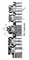
- the conventional DSL processmay create a transitional region or area, as shown in FIG. 1 below, where the two different types of liners overlap.
- FIG. 1is a simplified illustration of a dual stress liner formed by following a conventional DSL process.
- a semiconductor chip or semiconductor structure 10may have two device regions 11 and 12 wherein two different types of transistors maybe manufactured.
- a first type of stress liner 21may be formed to cover transistors in device region 11
- a second type of stress liner 23may be formed to cover transistors in device region 12 .
- Stress liners 21 and 23which together forms the dual stress liner, may be nitride stress liners and may be compressive and/or tensile stress liners. Stress liner 21 may be covered by an oxide layer 22 . In a transitional region or area 20 , as is illustrated in FIG.
- Transitional region 20may form a tri-layer stack of nitride/oxide/nitride material, with a thickness that is thicker than either stress liner 21 or stress liner 23 .
- FIG. 1is a simplified illustration of a conventional dual stress liner having a stack of stress liners in a transitional region
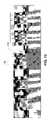
- FIG. 2is a simplified illustration of a self-aligned dual segment liner formed according to one embodiment of the present invention.
- FIGS. 3-14are simplified illustrations of methods and/or processes of forming a self-aligned dual segment liner according to one embodiment of the present invention.
- Embodiments of the present inventionprovide a semiconductor structure with a self-aligned dual segment liner, and method of making the same.
- one embodiment of the inventionprovides a method of forming a dual segment liner covering a first and a second set of semiconductor devices.
- the methodincludes forming a first liner and a first protective layer on top thereof, the first liner covering the first set of semiconductor devices; forming a second liner, the second liner having a first section covering the first protective layer, a transitional section, and a second section covering the second set of semiconductor devices, the second section being self-aligned to the first liner via the transitional section; forming a second protective layer on top of the second section of second liner; removing the first section and at least part of the transitional section of the second liner; and obtaining the dual segment liner including the first liner, the transitional section and the second section of the second liner.
- forming the second protective layer on top of the second section of the second linerincludes depositing the second protective layer on top of the second liner; and recessing a top surface of the second protective layer to expose the first section and the transitional section of the second liner.
- recessing the top surface of the second protective layerincludes applying a chemical-mechanical-polishing (CMP) process to remove the second protective layer on top of the first section and the transitional section of the second liner.
- CMPchemical-mechanical-polishing
- forming the first liner and the first protective layer on top thereof covering the first set of semiconductor devicesincludes forming the first liner that covers the first and second sets of semiconductor devices; forming the first protective layer on top of the first liner; and removing a portion of the first protective layer and a portion of the first liner to expose the second set of semiconductor devices.
- removing the first section and at least part of the transitional section of the second linerincludes applying a selective etching process to the first section and the transitional section of the second liner; monitoring a content level of exhaust gases from a the selective etching process; and continuing the selective etching process until the content level of the exhaust gases exhibits a drop.
- removing the first section and at least part of the transitional section of the second linerincludes applying non-selectively etching the first section, the transitional section, and the second protective layer on top of the second section of said second liner; monitoring a content level of exhaust gases from the non-selective etching; and terminating the non-selective etching when the content level of exhaust gases exhibits a pre-determined pattern of change.
- Embodiment of the inventionalso provides a semiconductor structure having a first and a second set of semiconductor devices fabricated on a semiconductor substrate.
- the semiconductor structureincludes a first liner covering the first set of semiconductor devices; and a second liner covering the second set of semiconductor devices, wherein the first and the second liners are self-aligned to form a dual segment liner.
- the first set of semiconductor devicesare in a first device region, and the second set of semiconductor devices are in a second device region, and wherein the first and second liners are self-aligned outside the first and the second device regions.
- the first lineris a compressive stress liner and the second liner is a tensile stress liner.
- CMOS field-effect-transistors of NFETs and PFETsmay be created or formed on a single substrate of a semiconductor chip by applying FEOL processing technologies.
- Well-known FEOL technologiesmay include processing steps and/or operations of, for example, cap deposition, photo-resist-mask formation, photolithography, hard-mask formation, wet etching, reactive-ion etching (RIE), ion-implantation, and chemical-mechanical polishing (CMP), to list a few.
- stress liners of the same or different typesmay be applied to the transistors, i.e., NFETs and PFETs, for device performance improvement. Improvement in device performance may come from improved mobility of electrons in a channel region of NFETs and/or holes in a channel region of PFETs brought by stresses induced by the stress liners.
- FIG. 2is a simplified illustration of a self-aligned dual segment liner formed according to one embodiment of the present invention.
- a semiconductor chip or semiconductor structure 100may include one or more device regions, for example device regions 101 and 201 , which may be covered by a first liner 140 and a second liner 180 respectively.
- Liners 140 and 180may together form the self-aligned dual segment liner.
- the self-aligned dual segment linermay be a portion of, or may form a part of, a multi-segment liner.
- Liners 140 and/or 180may be nitride liners.
- the present inventionis not limited in this respect and other liner materials may be used.
- Liners 140 and/or 180may be stress liners or unstressed liners; may be compressive stress liners or tensile stress liners; may have the same or different types of stresses; and may have the same or different levels of stresses.
- the self-aligned dual segment linermay be a self-aligned dual stress liner (SADSL).
- liners 140 and 180are assumed to be liners of different stresses and are referred to as stress liners 140 and 180 . However, as is described above, stress liners 140 and/or 180 may not need to be stress liners.
- the self-aligned dual segment liner formed by stress liners 140 and 180may be referred to as a self-aligned dual stress liner, or a SADSL.
- SADSLself-aligned dual stress liner
- stress liner 180is self-aligned with stress liner 140 .
- stress liner 140is self-aligned with stress liner 180 and there is little or no overlap between stress liners 140 and 180 in a transitional region 182 .
- This distinctive feature of the SADSL formed by stress liners 140 and 180shall be easily appreciated when being compared with the conventional DSL shown in FIG. 1 .
- a person skilled in the artwill appreciate that the at least partial removal and/or complete elimination of stress liner overlap in transitional region 182 , in contrary to that in a conventional DSL ( FIG. 1 ), may significantly simplify a process of forming contacts in device regions 101 and 201 for transistors ( 110 , 120 , 210 , and 220 ) and in an inter-connect region ( 310 ) of semiconductor structure 100 ( FIG. 3 ).
- FIGS. 3-14are simplified illustrations of methods and/or processes of forming a self-aligned dual segment liner, or a self-aligned dual stress liner, in accordance with embodiments of the invention.
- a methodmay include forming a self-aligned dual stress liner on top of a first set of FETs, e.g., a set of NFETs, and a second set of FETs, e.g., a set of PFETs.
- a first set of FETse.g., a set of NFETs
- a second set of FETse.g., a set of PFETs.
- a person skilled in the artwill appreciate that the present invention is not limited in this respect and embodiments of a method may include forming a self-aligned dual stress liner on other semiconductor devices other than and in addition to transistors or FETs.
- the present inventionis not limited to stress liners, and may be used to form or manufacture other types of liners of two or more different types or properties, either stressed or unstressed.
- the term “set”may include one.
- a set of FETsmay include only one FET.
- FIG. 3shows a semiconductor structure (chip) 100 that includes, among others, a combination of transistors such as NFETs and PFETs.
- structure 100may include an NFET 110 having a gate electrode 112 formed on top of a gate dielectric 111 .
- spacers 114 and 115may be nitride spacers with reduced width.
- silicidationmay be conducted forming conductive silicide layers over its source, drain, and gate regions, as shown in FIG. 3 .
- structure (chip) 100may include one or more other NFETs, for example a NFET 120 , having similar gate structures as NFET 110 .
- NFETs 110 and 120may be created or formed on top of a p-doped device region 101 .
- FIG. 3also illustrates that structure (chip) 100 may include a PFET 210 having a gate electrode 212 formed on top of a gate dielectric 211 with spacers 214 and 215 formed at the sides of gate electrode 212 .
- silicidationmay be conducted forming conductive silicide layers over its source, drain, and gate regions, as shown in FIG. 3 .
- source and drain regions of PFET 210may be covered by silicide layers 216 and 217
- gate electrode 212may be covered by silicide layer 213 .
- structure (chip) 100may include one or more other PFETs, for example a PFET 220 , having similar gate structures as PFET 220 .
- PFETs 210 and 220may be created or formed on top of an n-doped device region 201 .
- structure (chip) 100may further include one or more inter-connect structures, such as a structure 310 , which may be formed on top of an insulated region such as, for example a shallow trench insulation (STI) region 301 .
- Inter-connect structure 310may be used in connecting electrically adjacent FETs or other active devices.
- Semiconductor structure 100 as shown in FIG. 3including NFETs 110 and 120 , PFETs 211 and 221 , and inter-connect structure 310 , may be formed by applying any well-known FEOL processes. Details of steps and/or operations of the FEOL processes are not described here in order not to obscure the presentation of essence of the present invention.
- semiconductor devicesi.e., NFETs 110 and 120 , PFETs 210 and 220 , and inter-connect 310 , may be covered by a self-aligned dual stress liner (SADSL).
- SADSLself-aligned dual stress liner
- a process of forming the SADSLmay be applied to any other combinations of NFET and/or PFET transistors; and/or any other number of NFET and/or PFET transistors; and/or any other suitable surface topologies of semiconductor devices or structures.
- FIG. 4illustrates that, according to one embodiment, a method may include forming a first liner 140 through a well-known process such as, for example, deposition on top of semiconductor structure 100 .
- First liner 140may cover the most surface of structure (chip) 100 , including at least NFETs 110 and 120 , PFETs 210 and 220 , and inter-connect 310 .
- First liner 140may be a layer of tensile nitride.
- first liner 140may be a layer of compressive nitride or a liner without stress.
- a methodmay include removing and replacing a portion of tensile nitride layer 140 , i.e., the portion on top of PFETs 210 and 220 , later with a second liner 180 ( FIG. 2 ) of compressive nitride.
- a methodmay include removing and replacing a portion of compressive nitride layer 140 , i.e., the portion on top of NFETs 110 and 120 , later with a second liner of tensile nitride liner (not shown).
- first liner 140is assumed to be a tensile nitride layer.
- Tensile nitride layer 140may have a thickness ranging from around 500 ⁇ to around 900 ⁇ , and preferably around 600 ⁇ .
- the inventionis not limited in this respect either, and other thicknesses, below 500 ⁇ or above 900 ⁇ , of tensile nitride layer 140 may be used to accommodate different design needs such as, for example, a particular requirement of stress level to be induced into channel regions of NFETs 110 and 120 .
- FIG. 5illustrates that after forming first stress liner 140 , one embodiment of a method may include forming a layer of oxide 150 covering a top surface 141 of first stress liner 140 .
- Oxide layer 150may be deposited through, for example, a sub-atmospheric chemical vapor deposition (SACVD) process although other well-known processes and/or techniques may be used as well.
- SACVDsub-atmospheric chemical vapor deposition
- Embodiment of a methodmay also include subsequently planarizing oxide layer 150 such that a top surface 151 of oxide layer 150 becomes co-planner with top surface 141 of first stress liner 140 .
- oxide layer 150may be planarized to have a suitable thickness above, rather than co-planner with, first stress liner 140 and thus may perform at least partially the function of a protective layer 160 ( FIG. 6 ).
- the planarization of oxide layer 150may be performed through a well-known chemical-mechanical-polishing (CMP) process, preferably a fixed abrasive CMP process, but the invention is not limited in this respect and other planarization process may be used.
- CMPchemical-mechanical-polishing
- the CMP processmay be controlled and/or terminated by utilizing the selectivity of oxide 150 , relative to nitride stress liner 140 , during the process of planarization.
- FIG. 6illustrates that after planarizing oxide layer 150 to have a co-planner surface 151 with first stress liner 140
- a methodmay include depositing a protective layer 160 , which may be a low-temperature oxide (LTO) layer, to cover first stress liner 140 and oxide layer 150 .
- Protective layer 160may be referred to as a cap layer, a cap oxide layer, or an etch-stop layer, and may protect first stress liner 140 underneath during a subsequent RIE process ( FIG. 10 ).
- Cap oxide layer 160may have a thickness of around 150 ⁇ .
- the present inventionis not limited in this respect and other thicknesses of cap oxide layer 160 , for example from 100 ⁇ to 300 ⁇ or a thickness suitable as an etch-stop layer and/or hard-mask layer may be used.
- FIG. 7illustrates that one embodiment of a method may include forming a layer of photo-resist material through, for example, a well-known spin-on process, on top of cap oxide layer 160 .
- the photo-resist materialmay be subsequently patterned by, for example, applying a photo-lithography technique, to create a photo-mask 170 .
- Photo-mask 170 and/or cap oxide layer 160may cover device region 101 to protect NFETs 110 and 120 during a subsequent etching process of oxide. It shall be noted that a person skilled in the art will appreciate that protective layers of other materials, other than photo-resist and oxide, may be used as well to provide adequate protection for device region 101 of NFETs 110 and 120 .
- an anti-reflection-coatingmay be applied on top of cap oxide layer 160 , prior to the spin-on of photo-resist material, to improve the precision control of photo-mask patterning.
- first stress liner 140is a compressive nitride layer
- one embodiment of a methodmay include creating a photo-mask that covers and therefore protects device region 201 of PFETs 210 and 220 , instead of device region 101 of NFETs 110 and 120 .
- photo-mask 170may cover at least a portion of inter-connect structure 310 where first stress liner 140 is self-aligned to second stress liner 180 .
- FIG. 8illustrates that following forming photo-mask 170
- one embodiment of a methodmay include removing cap oxide layer 160 and oxide layer 150 , which cover device region 201 of PFETs 210 and 220 and are not covered by photo-mask 170 , through for example an etching process.
- the etching processmay be any well-known etching processes such as, for example, a reactive-ion-etching (RIE) process that are selective (non-reactive) to nitride.
- RIEreactive-ion-etching
- the selectivity of etchingmay be achieved by applying a mixture of gases such as, for example, C 4 F 8 , O 2 , Ar, and/or other suitable C x F y chemistry and by adjusting RF power and bias used in the etching process.
- the RIE processmay be monitored and promptly terminated upon detection of a dramatic change in the content mixture of exhaust gases coming out of a chamber wherein the RIE is conducted.
- Such dramatic change in content mixture of exhaust gasesmay be an indication that at least most part of first stress liner 140 covering PFETs 210 and 220 may have been exposed.
- FIGS. 9 and 10illustrate that after RIE of cap oxide layer 160 and oxide layer 150
- a methodmay include stripping off photo-mask 170 so that cap oxide layer 160 is exposed.
- a methodmay include removing the exposed portion of first stress liner 140 of tensile nitride by applying cap oxide layer 160 as a protective layer or hard-mask.
- the removing processmay be an etching process, such as a RIE process, that is designed to be selective (non-reactive) to oxide to expose PFETs 210 and 220 underneath.
- the selectivity of etchingmay be achieved by applying a mixture of gases such as, for example, CH 3 F, CH 2 F 2 , CHF 3 , CF 4 , Ar, O 2 , CO, and/or other suitable CH x F y chemistry, and by adjusting RF power and bias used in the etching process.
- the exposed portion of first stress liner 140may be removed before photo-mask 170 is stripped off, and thus photo-mask 170 may be used, at least partially, as a hard-mask in the RIE process of first stress liner 140 .
- cap oxide layer 160may be optionally removed by applying a selective RIE process.
- one embodiment of a methodmay include depositing a second liner 180 following the exposure of PFETs 210 and 220 after etching away the exposed portion of first stress liner 140 , as shown in FIG. 10 .
- Second liner 180may be a layer of compressive nitride liner 180 that is suitable for PFETs 210 and 220 .
- Stress liner 180may include a first section 183 on top of cap oxide layer 160 , a second section 184 on top of PFETs 210 and 220 , and a transitional section 182 between the first and second sections. Stress liner 180 may have a thickness ranging from around 500 ⁇ to around 700 ⁇ , and preferably around 600 ⁇ .
- the inventionis not limited in this respect and other thicknesses, below 500 ⁇ or above 700 ⁇ , may be used to accommodate different design needs such as, for example, a particular requirement of stress level to be induced into channel regions of PFET 210 and 220 .
- the second section 184 of compressive stress liner 180on top of PFETs 210 and 220 , may be self-aligned with the tensile stress liner 140 , under cap oxide layer 160 , through transitional section 182 .
- Transitional section 182may be formed on top of inter-connect structure 310 .
- transitional section 182may be formed on any other areas by design, normally from active semiconductor devices such as away from devices 110 , 120 , 210 , and 220 ( FIG. 3 ).
- transitional section 182may be formed (not shown) directly on top of a shallow trench region (STI).
- STIshallow trench region
- FIG. 12illustrates that, following depositing stress liner 180 , one embodiment of a method may include forming a protective layer 190 , such as oxide, to cover the top surface of stress liner 180 across device regions 101 and 201 .
- a protective layer 190such as oxide
- the formation of protective layer 190may be through a well-known process such as, for example, a SACVD process.
- one embodiment of a methodmay include recessing protective layer 190 such that a top surface 191 of protective layer 190 of oxide becomes co-planner with the top surface of first section 183 of stress liner 180 , which is on top of cap oxide layer 160 covering NFETs 110 and 120 .
- the recessing of protective layer 190may be performed through a planarization process such as a well-known chemical-mechanical-polishing (CMP) process, preferably a fixed abrasive CMP process.
- CMPchemical-mechanical-polishing
- the CMP processmay apply the selectivity of oxide of protective layer 190 , relative to stress liner 180 , to stop at the top surface of first section 183 of stress liner 180 .
- one embodiment of a methodmay include optionally planarizing protective layer 190 , if needed, to create a relatively flat top surface, then performing non-selective etching to expose the top surface of first section 183 of stress liner 180 as shown in FIG. 12 , and continuing performing the non-selective etching until a top surface 141 of stress liner 140 and a top surface 181 of stress liner 180 are exposed, as shown in FIG. 14 .
- the non-selective etchingmay be controlled, as is well known in the art, by timing, and/or by monitoring content levels of exhaust gases from the etching process until the level of a particular content such as, for example, N 2 and/or O 2 exhibits a pre-determined pattern of change such as a drop or an increase, at that point the non-selective etching process may be terminated.
- a particular contentsuch as, for example, N 2 and/or O 2 exhibits a pre-determined pattern of change such as a drop or an increase
- FIG. 13illustrates that following the planarizaiton of protective layer 190 , one embodiment of a method may include removing and/or etching away the exposed first section 183 of stress liner 180 , which is a compressive stress liner undesirable for NFETs 110 and 120 in device region 101 .
- Oxide protective layer 190may protect the second section 184 of stress liner 180 during the etching process of first section 183 of stress liner 180 .
- the etching processmay be a RIE process and may be end-pointed through monitoring content of exhaust gases from the RIE process.
- the RIE processmay be promptly stopped or terminated. This is because a sharp drop in the nitride content may be an indication that at least most of the exposed nitride liner 180 (first section 183 ), on top of cap oxide layer 160 , may have been etched away.
- the RIE processshall be stopped or terminated promptly once the exposed stress liner 180 above the NFET device region 101 is etched away such as not to over-etch the stress liner 180 in transitional section 182 .
- One embodiment of a methodmay include timing the RIE process such that a predetermined thickness of nitride, approximately equal to or less than that of cap oxide layer 160 , may be removed to make nitride stress liner 180 at transitional section 182 have approximately the same thickness as the rest of nitride stress liner 180 .
- First stress liner 140 together with both transitional section 182 and second section 184 of second stress liner 180form a self-aligned dual stress liner (SADSL).
- SADSLself-aligned dual stress liner
- FIG. 14further illustrates that after removing first section 183 of compressive stress liner 180 in NFET device region 101 , one embodiment of a method may include optionally planarizing oxide layer 190 to be approximately co-plannar with top surface 141 of tensile stress liner 140 and top surface 181 of compressive stress liner 180 .
- the co-planner surfacemay be prepared to form subsequent inter-connect structures thereupon.
- Processes used in the planarizationmay be any well-known processes such as, for example, a CMP process.
- oxide protective layer 160 , oxide layer 150 , and oxide protective layer 190may be selectively (relative to nitride stress liner 140 and 180 ) etched away, for example, by applying a RIE process as described above to form semiconductor structure (chip) 100 as shown in FIG. 2 .
Landscapes
- Engineering & Computer Science (AREA)
- Physics & Mathematics (AREA)
- Condensed Matter Physics & Semiconductors (AREA)
- General Physics & Mathematics (AREA)
- Manufacturing & Machinery (AREA)
- Computer Hardware Design (AREA)
- Microelectronics & Electronic Packaging (AREA)
- Power Engineering (AREA)
- Internal Circuitry In Semiconductor Integrated Circuit Devices (AREA)
- Metal-Oxide And Bipolar Metal-Oxide Semiconductor Integrated Circuits (AREA)
Abstract
Description
Claims (14)
Priority Applications (2)
| Application Number | Priority Date | Filing Date | Title |
|---|---|---|---|
| US11/468,536US7482215B2 (en) | 2006-08-30 | 2006-08-30 | Self-aligned dual segment liner and method of manufacturing the same |
| CN2007101364081ACN101136371B (en) | 2006-08-30 | 2007-07-16 | Self-aligned dual-segment liner and method of manufacturing the same |
Applications Claiming Priority (1)
| Application Number | Priority Date | Filing Date | Title |
|---|---|---|---|
| US11/468,536US7482215B2 (en) | 2006-08-30 | 2006-08-30 | Self-aligned dual segment liner and method of manufacturing the same |
Publications (2)
| Publication Number | Publication Date |
|---|---|
| US20080054413A1 US20080054413A1 (en) | 2008-03-06 |
| US7482215B2true US7482215B2 (en) | 2009-01-27 |
Family
ID=39150327
Family Applications (1)
| Application Number | Title | Priority Date | Filing Date |
|---|---|---|---|
| US11/468,536Expired - Fee RelatedUS7482215B2 (en) | 2006-08-30 | 2006-08-30 | Self-aligned dual segment liner and method of manufacturing the same |
Country Status (2)
| Country | Link |
|---|---|
| US (1) | US7482215B2 (en) |
| CN (1) | CN101136371B (en) |
Cited By (10)
| Publication number | Priority date | Publication date | Assignee | Title |
|---|---|---|---|---|
| US20080057720A1 (en)* | 2006-08-31 | 2008-03-06 | Kai Frohberg | Method for patterning contact etch stop layers by using a planarization process |
| US20080081476A1 (en)* | 2006-09-28 | 2008-04-03 | Samsung Electronics Co., Ltd. | Methods of Forming Integrated Circuit Devices Having Tensile and Compressive Stress Layers Therein and Devices Formed Thereby |
| US20090081837A1 (en)* | 2007-09-26 | 2009-03-26 | Advanced Micro Devices, Inc. | Method for fabricating a semiconductor device having an extended stress liner |
| US20090081840A1 (en)* | 2007-09-20 | 2009-03-26 | Samsung Electronics Co., Ltd. | Method of Forming Field Effect Transistors Using Diluted Hydrofluoric Acid to Remove Sacrificial Nitride Spacers |
| US20090101979A1 (en)* | 2007-10-17 | 2009-04-23 | Samsung Electronics Co., Ltd. | Methods of Forming Field Effect Transistors Having Stress-Inducing Sidewall Insulating Spacers Thereon and Devices Formed Thereby |
| US20090124093A1 (en)* | 2006-11-16 | 2009-05-14 | Samsung Electronics Co., Ltd. | Methods of Forming CMOS Integrated Circuits that Utilize Insulating Layers with High Stress Characteristics to Improve NMOS and PMOS Transistor Carrier Mobilities |
| US20090194817A1 (en)* | 2007-03-27 | 2009-08-06 | Samsung Electronics Co., Ltd. | CMOS Integrated Circuit Devices Having Stressed NMOS and PMOS Channel Regions Therein |
| US20090289375A1 (en)* | 2006-07-05 | 2009-11-26 | Toshiba America Electronic Components, Inc. | Dual Stress Liner Device and Method |
| US20090309164A1 (en)* | 2008-06-16 | 2009-12-17 | International Business Machines Corporation | Structure and method to integrate dual silicide with dual stress liner to improve cmos performance |
| US20110180882A1 (en)* | 2006-09-29 | 2011-07-28 | Kabushiki Kaisha Toshiba | Semiconductor Device and Method of Fabricating the Same |
Families Citing this family (13)
| Publication number | Priority date | Publication date | Assignee | Title |
|---|---|---|---|---|
| US7436169B2 (en)* | 2005-09-06 | 2008-10-14 | International Business Machines Corporation | Mechanical stress characterization in semiconductor device |
| KR100772902B1 (en)* | 2006-09-28 | 2007-11-05 | 삼성전자주식회사 | Semiconductor device and manufacturing method thereof |
| US20090014807A1 (en)* | 2007-07-13 | 2009-01-15 | Chartered Semiconductor Manufacturing, Ltd. | Dual stress liners for integrated circuits |
| JP2009027008A (en)* | 2007-07-20 | 2009-02-05 | Panasonic Corp | Semiconductor device and manufacturing method thereof |
| CN102386130B (en)* | 2010-09-02 | 2013-09-11 | 中芯国际集成电路制造(上海)有限公司 | Forming method of dual-stress liner semiconductor device |
| CN105789114B (en)* | 2012-09-24 | 2019-05-03 | 中芯国际集成电路制造(上海)有限公司 | Semiconductor device and method of manufacturing the same |
| FR3007196A1 (en)* | 2013-06-13 | 2014-12-19 | St Microelectronics Rousset | ACTIVE NMOS TRANSISTOR WITH COMPRESSED COMPRESSION CONSTRAINTS |
| FR3007198B1 (en) | 2013-06-13 | 2015-06-19 | St Microelectronics Rousset | COMPONENT, FOR EXAMPLE NMOS TRANSISTOR, ACTIVE REGION WITH RELEASED COMPRESSION STRESSES, AND METHOD OF MANUFACTURING |
| US9105559B2 (en) | 2013-09-16 | 2015-08-11 | International Business Machines Corporation | Conformal doping for FinFET devices |
| FR3018139B1 (en) | 2014-02-28 | 2018-04-27 | Stmicroelectronics (Rousset) Sas | COMPONENT INTEGRATED CIRCUIT, FOR EXAMPLE NMOS TRANSISTORS, WITH ACTIVATED REGIONS WITH COMPRESSED COMPRESSION STRESSES |
| FR3025335B1 (en) | 2014-08-29 | 2016-09-23 | Stmicroelectronics Rousset | METHOD FOR MANUFACTURING AN INTEGRATED CIRCUIT FOR IMPROVING INTEGRATED CIRCUIT RETRO-DESIGN AND CORRESPONDING INTEGRATED CIRCUIT |
| US11133248B2 (en)* | 2019-11-11 | 2021-09-28 | Xia Tai Xin Semiconductor (Qing Dao) Ltd. | Semiconductor structure and method for fabricating the same |
| CN118315344B (en)* | 2024-06-07 | 2024-08-02 | 杭州积海半导体有限公司 | Method for forming semiconductor device |
Citations (15)
| Publication number | Priority date | Publication date | Assignee | Title |
|---|---|---|---|---|
| US4732871A (en) | 1986-07-11 | 1988-03-22 | International Business Machines Corporation | Process for producing undercut dummy gate mask profiles for MESFETs |
| US4880684A (en) | 1988-03-11 | 1989-11-14 | International Business Machines Corporation | Sealing and stress relief layers and use thereof |
| US4958213A (en) | 1987-12-07 | 1990-09-18 | Texas Instruments Incorporated | Method for forming a transistor base region under thick oxide |
| US5134085A (en) | 1991-11-21 | 1992-07-28 | Micron Technology, Inc. | Reduced-mask, split-polysilicon CMOS process, incorporating stacked-capacitor cells, for fabricating multi-megabit dynamic random access memories |
| US5221637A (en) | 1991-05-31 | 1993-06-22 | Interuniversitair Micro Elektronica Centrum Vzw | Mesa release and deposition (MRD) method for stress relief in heteroepitaxially grown GaAs on Si |
| US5516721A (en) | 1993-12-23 | 1996-05-14 | International Business Machines Corporation | Isolation structure using liquid phase oxide deposition |
| US5559357A (en) | 1992-09-21 | 1996-09-24 | Krivokapic; Zoran | Poly LDD self-aligned channel transistors |
| US5920780A (en) | 1997-01-31 | 1999-07-06 | Mosel Vitelic Incorporated | Method of forming a self aligned contact (SAC) window |
| US5981383A (en) | 1996-03-18 | 1999-11-09 | United Microelectronics Corporation | Method of fabricating a salicide layer of a device electrode |
| US6040223A (en) | 1999-08-13 | 2000-03-21 | Taiwan Semiconductor Manufacturing Company | Method for making improved polysilicon FET gate electrodes having composite sidewall spacers using a trapezoidal-shaped insulating layer for more reliable integrated circuits |
| US6316349B1 (en) | 1998-11-12 | 2001-11-13 | Hyundai Electronics Industries Co., Ltd. | Method for forming contacts of semiconductor devices |
| US6366468B1 (en) | 2000-04-28 | 2002-04-02 | Hewlett-Packard Company | Self-aligned common carrier |
| US6704185B2 (en) | 2000-02-23 | 2004-03-09 | National Center For Scientific Research | Capacitive pressure-responsive devices and their fabrication |
| US6849502B2 (en) | 2002-06-21 | 2005-02-01 | Hitachi, Ltd. | Semiconductor device and method of manufacturing the same |
| US7101744B1 (en) | 2005-03-01 | 2006-09-05 | International Business Machines Corporation | Method for forming self-aligned, dual silicon nitride liner for CMOS devices |
Family Cites Families (3)
| Publication number | Priority date | Publication date | Assignee | Title |
|---|---|---|---|---|
| TW400561B (en)* | 1998-06-08 | 2000-08-01 | United Microelectronics Corp | The manufacturing method of the self-aligned salicide |
| US6573172B1 (en)* | 2002-09-16 | 2003-06-03 | Advanced Micro Devices, Inc. | Methods for improving carrier mobility of PMOS and NMOS devices |
| US7288451B2 (en)* | 2005-03-01 | 2007-10-30 | International Business Machines Corporation | Method and structure for forming self-aligned, dual stress liner for CMOS devices |
- 2006
- 2006-08-30USUS11/468,536patent/US7482215B2/ennot_activeExpired - Fee Related
- 2007
- 2007-07-16CNCN2007101364081Apatent/CN101136371B/ennot_activeExpired - Fee Related
Patent Citations (16)
| Publication number | Priority date | Publication date | Assignee | Title |
|---|---|---|---|---|
| US4732871A (en) | 1986-07-11 | 1988-03-22 | International Business Machines Corporation | Process for producing undercut dummy gate mask profiles for MESFETs |
| US4958213A (en) | 1987-12-07 | 1990-09-18 | Texas Instruments Incorporated | Method for forming a transistor base region under thick oxide |
| US4880684A (en) | 1988-03-11 | 1989-11-14 | International Business Machines Corporation | Sealing and stress relief layers and use thereof |
| US5221637A (en) | 1991-05-31 | 1993-06-22 | Interuniversitair Micro Elektronica Centrum Vzw | Mesa release and deposition (MRD) method for stress relief in heteroepitaxially grown GaAs on Si |
| US5134085A (en) | 1991-11-21 | 1992-07-28 | Micron Technology, Inc. | Reduced-mask, split-polysilicon CMOS process, incorporating stacked-capacitor cells, for fabricating multi-megabit dynamic random access memories |
| US5559357A (en) | 1992-09-21 | 1996-09-24 | Krivokapic; Zoran | Poly LDD self-aligned channel transistors |
| US5571738A (en) | 1992-09-21 | 1996-11-05 | Advanced Micro Devices, Inc. | Method of making poly LDD self-aligned channel transistors |
| US5516721A (en) | 1993-12-23 | 1996-05-14 | International Business Machines Corporation | Isolation structure using liquid phase oxide deposition |
| US5981383A (en) | 1996-03-18 | 1999-11-09 | United Microelectronics Corporation | Method of fabricating a salicide layer of a device electrode |
| US5920780A (en) | 1997-01-31 | 1999-07-06 | Mosel Vitelic Incorporated | Method of forming a self aligned contact (SAC) window |
| US6316349B1 (en) | 1998-11-12 | 2001-11-13 | Hyundai Electronics Industries Co., Ltd. | Method for forming contacts of semiconductor devices |
| US6040223A (en) | 1999-08-13 | 2000-03-21 | Taiwan Semiconductor Manufacturing Company | Method for making improved polysilicon FET gate electrodes having composite sidewall spacers using a trapezoidal-shaped insulating layer for more reliable integrated circuits |
| US6704185B2 (en) | 2000-02-23 | 2004-03-09 | National Center For Scientific Research | Capacitive pressure-responsive devices and their fabrication |
| US6366468B1 (en) | 2000-04-28 | 2002-04-02 | Hewlett-Packard Company | Self-aligned common carrier |
| US6849502B2 (en) | 2002-06-21 | 2005-02-01 | Hitachi, Ltd. | Semiconductor device and method of manufacturing the same |
| US7101744B1 (en) | 2005-03-01 | 2006-09-05 | International Business Machines Corporation | Method for forming self-aligned, dual silicon nitride liner for CMOS devices |
Cited By (20)
| Publication number | Priority date | Publication date | Assignee | Title |
|---|---|---|---|---|
| US20090289375A1 (en)* | 2006-07-05 | 2009-11-26 | Toshiba America Electronic Components, Inc. | Dual Stress Liner Device and Method |
| US8004035B2 (en)* | 2006-07-05 | 2011-08-23 | Kabushiki Kaisha Toshiba | Dual stress liner device and method |
| US7838354B2 (en)* | 2006-08-31 | 2010-11-23 | Advanced Micro Devices, Inc. | Method for patterning contact etch stop layers by using a planarization process |
| US20080057720A1 (en)* | 2006-08-31 | 2008-03-06 | Kai Frohberg | Method for patterning contact etch stop layers by using a planarization process |
| US20080081476A1 (en)* | 2006-09-28 | 2008-04-03 | Samsung Electronics Co., Ltd. | Methods of Forming Integrated Circuit Devices Having Tensile and Compressive Stress Layers Therein and Devices Formed Thereby |
| US7785951B2 (en)* | 2006-09-28 | 2010-08-31 | Samsung Electronics Co., Ltd. | Methods of forming integrated circuit devices having tensile and compressive stress layers therein and devices formed thereby |
| US20110180882A1 (en)* | 2006-09-29 | 2011-07-28 | Kabushiki Kaisha Toshiba | Semiconductor Device and Method of Fabricating the Same |
| US7781276B2 (en) | 2006-11-16 | 2010-08-24 | Samsung Electronics Co., Ltd. | Methods of forming CMOS integrated circuits that utilize insulating layers with high stress characteristics to improve NMOS and PMOS transistor carrier mobilities |
| US20090124093A1 (en)* | 2006-11-16 | 2009-05-14 | Samsung Electronics Co., Ltd. | Methods of Forming CMOS Integrated Circuits that Utilize Insulating Layers with High Stress Characteristics to Improve NMOS and PMOS Transistor Carrier Mobilities |
| US20090194817A1 (en)* | 2007-03-27 | 2009-08-06 | Samsung Electronics Co., Ltd. | CMOS Integrated Circuit Devices Having Stressed NMOS and PMOS Channel Regions Therein |
| US7800134B2 (en) | 2007-03-27 | 2010-09-21 | Samsung Electronics Co., Ltd. | CMOS integrated circuit devices having stressed NMOS and PMOS channel regions therein |
| US7902082B2 (en) | 2007-09-20 | 2011-03-08 | Samsung Electronics Co., Ltd. | Method of forming field effect transistors using diluted hydrofluoric acid to remove sacrificial nitride spacers |
| US20090081840A1 (en)* | 2007-09-20 | 2009-03-26 | Samsung Electronics Co., Ltd. | Method of Forming Field Effect Transistors Using Diluted Hydrofluoric Acid to Remove Sacrificial Nitride Spacers |
| US7761838B2 (en)* | 2007-09-26 | 2010-07-20 | Globalfoundries Inc. | Method for fabricating a semiconductor device having an extended stress liner |
| US20090081837A1 (en)* | 2007-09-26 | 2009-03-26 | Advanced Micro Devices, Inc. | Method for fabricating a semiconductor device having an extended stress liner |
| US20090101979A1 (en)* | 2007-10-17 | 2009-04-23 | Samsung Electronics Co., Ltd. | Methods of Forming Field Effect Transistors Having Stress-Inducing Sidewall Insulating Spacers Thereon and Devices Formed Thereby |
| US7923365B2 (en) | 2007-10-17 | 2011-04-12 | Samsung Electronics Co., Ltd. | Methods of forming field effect transistors having stress-inducing sidewall insulating spacers thereon |
| US20110156110A1 (en)* | 2007-10-17 | 2011-06-30 | Jun-Jung Kim | Field Effect Transistors Having Gate Electrode Silicide Layers with Reduced Surface Damage |
| US20090309164A1 (en)* | 2008-06-16 | 2009-12-17 | International Business Machines Corporation | Structure and method to integrate dual silicide with dual stress liner to improve cmos performance |
| US7960223B2 (en)* | 2008-06-16 | 2011-06-14 | International Business Machines Corporation | Structure and method to integrate dual silicide with dual stress liner to improve CMOS performance |
Also Published As
| Publication number | Publication date |
|---|---|
| US20080054413A1 (en) | 2008-03-06 |
| CN101136371B (en) | 2010-06-09 |
| CN101136371A (en) | 2008-03-05 |
Similar Documents
| Publication | Publication Date | Title |
|---|---|---|
| US7482215B2 (en) | Self-aligned dual segment liner and method of manufacturing the same | |
| KR100868098B1 (en) | Methods of forming integrated circuit devices, method of forming semiconductor devices, and semiconductor devices formed thereby | |
| US7410854B2 (en) | Method of making FUSI gate and resulting structure | |
| US7446026B2 (en) | Method of forming a CMOS device with stressor source/drain regions | |
| US20160049490A1 (en) | Integrated circuits with dual silicide contacts and methods for fabricating same | |
| US20070200179A1 (en) | Strain enhanced CMOS architecture with amorphous carbon film and fabrication method of forming the same | |
| US6716689B2 (en) | MOS transistor having a T-shaped gate electrode and method for fabricating the same | |
| US20080064173A1 (en) | Semiconductor device, cmos device and fabricating methods of the same | |
| US7943454B2 (en) | Method for dual stress liner | |
| US9318445B2 (en) | Semiconductor device and manufacturing method thereof for protecting metal-gate from oxidation | |
| WO2006135548A2 (en) | Method of forming an interlayer dielectric | |
| US20070099360A1 (en) | Integrated circuits having strained channel field effect transistors and methods of making | |
| KR100772902B1 (en) | Semiconductor device and manufacturing method thereof | |
| US20090101979A1 (en) | Methods of Forming Field Effect Transistors Having Stress-Inducing Sidewall Insulating Spacers Thereon and Devices Formed Thereby | |
| US7101744B1 (en) | Method for forming self-aligned, dual silicon nitride liner for CMOS devices | |
| US8609533B2 (en) | Methods for fabricating integrated circuits having substrate contacts and integrated circuits having substrate contacts | |
| US20070238238A1 (en) | CMOS device and fabricating method thereof | |
| US7589385B2 (en) | Semiconductor CMOS transistors and method of manufacturing the same | |
| US6958278B2 (en) | Semiconductor devices and methods for fabricating the same | |
| US7863693B2 (en) | Forming conductive stud for semiconductive devices | |
| US20140213028A1 (en) | Epitaxial process | |
| US20070152272A1 (en) | Method for fabricating a transistor using a soi wafer | |
| US9076818B2 (en) | Semiconductor device fabrication methods | |
| US8895403B2 (en) | Transistor, method for fabricating the transistor, and semiconductor device comprising the transistor | |
| CN101355054A (en) | Method for manufacturing complementary metal oxide semiconductor transistor |
Legal Events
| Date | Code | Title | Description |
|---|---|---|---|
| AS | Assignment | Owner name:INFINEON TECHNOLOGIES NORTH AMERICA CORP., CALIFOR Free format text:ASSIGNMENT OF ASSIGNORS INTEREST;ASSIGNOR:YAN, JIANG;REEL/FRAME:018246/0245 Effective date:20060824 Owner name:INTERNATIONAL BUSINESS MACHINES CORPORATION, NEW Y Free format text:ASSIGNMENT OF ASSIGNORS INTEREST;ASSIGNORS:DYER, THOMAS W.;FANG, SUNFEI;REEL/FRAME:018246/0248;SIGNING DATES FROM 20060824 TO 20060828 | |
| AS | Assignment | Owner name:INFINEON TECHNOLOGIES AG, GERMANY Free format text:ASSIGNMENT OF ASSIGNORS INTEREST;ASSIGNOR:INFINEON TECHNOLOGIES NORTH AMERICA CORP.;REEL/FRAME:019774/0898 Effective date:20070831 Owner name:INFINEON TECHNOLOGIES AG,GERMANY Free format text:ASSIGNMENT OF ASSIGNORS INTEREST;ASSIGNOR:INFINEON TECHNOLOGIES NORTH AMERICA CORP.;REEL/FRAME:019774/0898 Effective date:20070831 | |
| FEPP | Fee payment procedure | Free format text:PAYER NUMBER DE-ASSIGNED (ORIGINAL EVENT CODE: RMPN); ENTITY STATUS OF PATENT OWNER: LARGE ENTITY Free format text:PAYOR NUMBER ASSIGNED (ORIGINAL EVENT CODE: ASPN); ENTITY STATUS OF PATENT OWNER: LARGE ENTITY | |
| STCF | Information on status: patent grant | Free format text:PATENTED CASE | |
| REMI | Maintenance fee reminder mailed | ||
| FPAY | Fee payment | Year of fee payment:4 | |
| SULP | Surcharge for late payment | ||
| FPAY | Fee payment | Year of fee payment:8 | |
| FEPP | Fee payment procedure | Free format text:MAINTENANCE FEE REMINDER MAILED (ORIGINAL EVENT CODE: REM.); ENTITY STATUS OF PATENT OWNER: LARGE ENTITY | |
| LAPS | Lapse for failure to pay maintenance fees | Free format text:PATENT EXPIRED FOR FAILURE TO PAY MAINTENANCE FEES (ORIGINAL EVENT CODE: EXP.); ENTITY STATUS OF PATENT OWNER: LARGE ENTITY | |
| STCH | Information on status: patent discontinuation | Free format text:PATENT EXPIRED DUE TO NONPAYMENT OF MAINTENANCE FEES UNDER 37 CFR 1.362 | |
| FP | Lapsed due to failure to pay maintenance fee | Effective date:20210127 |