US7481887B2 - Apparatus for controlling gas pulsing in processes for depositing materials onto micro-device workpieces - Google Patents
Apparatus for controlling gas pulsing in processes for depositing materials onto micro-device workpiecesDownload PDFInfo
- Publication number
- US7481887B2 US7481887B2US11/027,809US2780904AUS7481887B2US 7481887 B2US7481887 B2US 7481887B2US 2780904 AUS2780904 AUS 2780904AUS 7481887 B2US7481887 B2US 7481887B2
- Authority
- US
- United States
- Prior art keywords
- precursor
- flow
- reaction chamber
- valve assembly
- purge gas
- Prior art date
- Legal status (The legal status is an assumption and is not a legal conclusion. Google has not performed a legal analysis and makes no representation as to the accuracy of the status listed.)
- Expired - Fee Related, expires
Links
- 238000000151depositionMethods0.000titleclaimsabstractdescription30
- 239000000463materialSubstances0.000titleclaimsabstractdescription29
- 238000000034methodMethods0.000titleclaimsdescription36
- 239000002243precursorSubstances0.000claimsabstractdescription225
- 238000010926purgeMethods0.000claimsabstractdescription130
- 238000006243chemical reactionMethods0.000claimsabstractdescription103
- 230000005855radiationEffects0.000claimsabstractdescription102
- 238000012544monitoring processMethods0.000claimsabstractdescription69
- 238000005259measurementMethods0.000claimsdescription23
- 230000002596correlated effectEffects0.000claimsdescription10
- 239000004065semiconductorSubstances0.000claimsdescription4
- 230000008021depositionEffects0.000abstractdescription7
- 239000007789gasSubstances0.000description106
- 239000010410layerSubstances0.000description22
- 238000000231atomic layer depositionMethods0.000description19
- 238000012545processingMethods0.000description11
- 238000005229chemical vapour depositionMethods0.000description8
- 230000001276controlling effectEffects0.000description7
- 230000000875corresponding effectEffects0.000description7
- 238000001179sorption measurementMethods0.000description7
- 239000007787solidSubstances0.000description6
- 239000000758substrateSubstances0.000description6
- 230000001965increasing effectEffects0.000description5
- 238000003795desorptionMethods0.000description4
- 239000010408filmSubstances0.000description4
- 238000007736thin film deposition techniqueMethods0.000description4
- 230000007423decreaseEffects0.000description3
- 238000005516engineering processMethods0.000description3
- 238000004519manufacturing processMethods0.000description3
- 239000010409thin filmSubstances0.000description3
- 239000000470constituentSubstances0.000description2
- 230000003247decreasing effectEffects0.000description2
- 238000005137deposition processMethods0.000description2
- 238000010586diagramMethods0.000description2
- 238000010438heat treatmentMethods0.000description2
- 238000004377microelectronicMethods0.000description2
- 238000002336sorption--desorption measurementMethods0.000description2
- 238000001228spectrumMethods0.000description2
- XUIMIQQOPSSXEZ-UHFFFAOYSA-NSiliconChemical compound[Si]XUIMIQQOPSSXEZ-UHFFFAOYSA-N0.000description1
- 239000011248coating agentSubstances0.000description1
- 238000000576coating methodMethods0.000description1
- 230000006835compressionEffects0.000description1
- 238000007906compressionMethods0.000description1
- 230000008878couplingEffects0.000description1
- 238000010168coupling processMethods0.000description1
- 238000005859coupling reactionMethods0.000description1
- 230000001351cycling effectEffects0.000description1
- 238000013500data storageMethods0.000description1
- 230000001627detrimental effectEffects0.000description1
- 230000002708enhancing effectEffects0.000description1
- 239000011521glassSubstances0.000description1
- 239000000203mixtureSubstances0.000description1
- 238000012986modificationMethods0.000description1
- 230000004048modificationEffects0.000description1
- 239000012713reactive precursorSubstances0.000description1
- 229910052710siliconInorganic materials0.000description1
- 239000010703siliconSubstances0.000description1
- 239000002356single layerSubstances0.000description1
- 238000000427thin-film depositionMethods0.000description1
- 238000012876topographyMethods0.000description1
- 238000007740vapor depositionMethods0.000description1
- 235000012431wafersNutrition0.000description1
Images


Classifications
- C—CHEMISTRY; METALLURGY
- C23—COATING METALLIC MATERIAL; COATING MATERIAL WITH METALLIC MATERIAL; CHEMICAL SURFACE TREATMENT; DIFFUSION TREATMENT OF METALLIC MATERIAL; COATING BY VACUUM EVAPORATION, BY SPUTTERING, BY ION IMPLANTATION OR BY CHEMICAL VAPOUR DEPOSITION, IN GENERAL; INHIBITING CORROSION OF METALLIC MATERIAL OR INCRUSTATION IN GENERAL
- C23C—COATING METALLIC MATERIAL; COATING MATERIAL WITH METALLIC MATERIAL; SURFACE TREATMENT OF METALLIC MATERIAL BY DIFFUSION INTO THE SURFACE, BY CHEMICAL CONVERSION OR SUBSTITUTION; COATING BY VACUUM EVAPORATION, BY SPUTTERING, BY ION IMPLANTATION OR BY CHEMICAL VAPOUR DEPOSITION, IN GENERAL
- C23C16/00—Chemical coating by decomposition of gaseous compounds, without leaving reaction products of surface material in the coating, i.e. chemical vapour deposition [CVD] processes
- C23C16/44—Chemical coating by decomposition of gaseous compounds, without leaving reaction products of surface material in the coating, i.e. chemical vapour deposition [CVD] processes characterised by the method of coating
- C23C16/455—Chemical coating by decomposition of gaseous compounds, without leaving reaction products of surface material in the coating, i.e. chemical vapour deposition [CVD] processes characterised by the method of coating characterised by the method used for introducing gases into reaction chamber or for modifying gas flows in reaction chamber
- C23C16/45523—Pulsed gas flow or change of composition over time
- C23C16/45525—Atomic layer deposition [ALD]
- C—CHEMISTRY; METALLURGY
- C23—COATING METALLIC MATERIAL; COATING MATERIAL WITH METALLIC MATERIAL; CHEMICAL SURFACE TREATMENT; DIFFUSION TREATMENT OF METALLIC MATERIAL; COATING BY VACUUM EVAPORATION, BY SPUTTERING, BY ION IMPLANTATION OR BY CHEMICAL VAPOUR DEPOSITION, IN GENERAL; INHIBITING CORROSION OF METALLIC MATERIAL OR INCRUSTATION IN GENERAL
- C23C—COATING METALLIC MATERIAL; COATING MATERIAL WITH METALLIC MATERIAL; SURFACE TREATMENT OF METALLIC MATERIAL BY DIFFUSION INTO THE SURFACE, BY CHEMICAL CONVERSION OR SUBSTITUTION; COATING BY VACUUM EVAPORATION, BY SPUTTERING, BY ION IMPLANTATION OR BY CHEMICAL VAPOUR DEPOSITION, IN GENERAL
- C23C16/00—Chemical coating by decomposition of gaseous compounds, without leaving reaction products of surface material in the coating, i.e. chemical vapour deposition [CVD] processes
- C23C16/44—Chemical coating by decomposition of gaseous compounds, without leaving reaction products of surface material in the coating, i.e. chemical vapour deposition [CVD] processes characterised by the method of coating
- C23C16/52—Controlling or regulating the coating process
Definitions
- the present inventionis related to apparatus and methods for controlling gas pulsing in thin film deposition processes used in the manufacturing of micro-devices.
- Thin film deposition techniquesare widely used in the manufacturing of micro-devices to form a coating on a workpiece that closely conforms to the surface topography.
- the size of the individual components in the devicesis constantly decreasing, and the number of layers in the devices is increasing.
- the density of components and the aspect ratios of depressionse.g., the ratio of the depth to the size of the opening
- the size of workpiecesis also increasing to provide more real estate for forming more dies (i.e., chips) on a single workpiece.
- Many fabricators, for exampleare transitioning from 200 mm to 300 mm workpieces, and even larger workpieces will likely be used in the future.
- Thin film deposition techniquesaccordingly strive to produce highly uniform conformal layers that cover the sidewalls, bottoms and corners in deep depressions that have very small openings.
- CVDChemical Vapor Deposition
- one or more precursors that are capable of reacting to form a solid thin filmare mixed in a gas or vapor state, and then the precursor mixture is presented to the surface of the workpiece.
- the surface of the workpiececatalyzes the reaction between the precursors to form a thin solid film at the workpiece surface.
- the most common way to catalyze the reaction at the surface of the workpieceis to heat the workpiece to a temperature that causes the reaction.
- CVD techniquesare useful in many applications, they also have several drawbacks. For example, if the precursors are not highly reactive, then a high workpiece temperature is needed to achieve a reasonable deposition rate. Such high temperatures are not typically desirable because heating the workpiece can be detrimental to the structures and other materials that are already formed on the workpiece. Implanted or doped materials, for example, can migrate in the silicon substrate at higher temperatures. On the other hand, if more reactive precursors are used so that the workpiece temperature can be lower, then reactions may occur prematurely in the gas phase before reaching the substrate. This is not desirable because the film quality and uniformity may suffer, and also because it limits the types of precursors that can be used. Thus, CVD techniques may not be appropriate for many thin film applications.
- FIGS. 1A and 1Bschematically illustrate the basic operation of ALD processes.
- a layer of gas molecules A xcoats the surface of a workpiece W.
- the layer of A x moleculesis formed by exposing the workpiece W to a precursor gas containing A x molecules, and then purging the chamber with a purge gas to remove excess A x molecules.
- This processcan form a monolayer of A x molecules on the surface of the workpiece W because the A x molecules at the surface are held in place during the purge cycle by physical adsorption forces at moderate temperatures or chemisorption forces at higher temperatures.
- the layer of A x moleculesis then exposed to another precursor gas containing B y molecules.
- the A x moleculesreact with the B y molecules to form an extremely thin solid layer of material on the workpiece W.
- the chamberis then purged again with a purge gas to remove excess By molecules.
- FIG. 2illustrates the stages of one cycle for forming a thin solid layer using ALD techniques.
- a typical cycleincludes (a) exposing the workpiece to the first precursor A x , (b) purging excess A x molecules, (c) exposing the workpiece to the second precursor B y , and then (d) purging excess B y molecules.
- each cyclemay form a layer having a thickness of approximately 0.5-1.0 ⁇ , and thus it takes approximately 60-120 cycles to form a solid layer having a thickness of approximately 60 ⁇ .
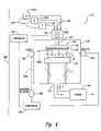
- FIG. 3schematically illustrates an ALD reactor 10 having a chamber 20 coupled to a gas supply 30 and a vacuum 40 .
- the reactor 10also includes a heater 50 that supports the workpiece W and a gas dispenser 60 in the chamber 20 .
- the gas dispenser 60includes a plenum 62 operatively coupled to the gas supply 30 and a distributor plate 70 having a plurality of holes 72 .
- the heater 50heats the workpiece W to a desired temperature
- the gas supply 30selectively injects the first precursor A x , the purge gas, and the second precursor B y as shown above in FIG. 2 .
- the vacuum 40maintains a negative pressure in the chamber to draw the gases from the gas dispenser 60 across the workpiece W and then through an outlet of the chamber 20 .
- ALD processinghas a relatively low throughput compared to CVD techniques.
- ALD processingtypically takes about eight to eleven seconds to perform each A x -purge-B y -purge cycle. This results in a total process time of approximately eight to eleven minutes to form a single thin layer of only 60 ⁇ .
- CVD techniquesonly require about one minute to form a 60 ⁇ thick layer.
- the low throughput of existing ALD techniqueslimits the utility of the technology in its current state because ALD may be a bottleneck in the overall manufacturing process. Thus, it would be useful to increase the throughput of ALD techniques so that they can be used in a wider range of applications.
- ALD processingis difficult to control the uniformity of the deposited films over a long period of time.
- One reason that it is difficult to consistently deposit uniform filmsis that the first precursor A x and/or the second precursor B y may ad sorb onto the surfaces of the reaction chamber 20 . This may cause a build up of the first and second precursors that produces a layer of the deposited material on the components of the reaction chamber 20 .
- the precursorswill then begin to desorp into the gas flows in the reaction chamber 20 .
- Such adsorption and desorption of the precursorsaffects the quality of the layers of material deposited onto the workpieces. Therefore, there is also a need to provide better control of ALD processing to achieve more consistent results throughout a run of workpieces.
- an apparatus for depositing materials onto a micro-device workpieceincludes a gas source system configured to provide a first precursor, a second precursor, and a purge gas.
- the apparatuscan also include a valve assembly coupled to the gas source system.
- the valve assemblyis configured to control a flow of the first precursor, a flow the second precursor, and a flow of the purge gas.
- Another component of the apparatusis a reaction chamber including an inlet coupled to the valve assembly, a workpiece holder in the reaction chamber, and an outlet downstream from the workpiece holder.
- the apparatusalso includes a monitoring system and a controller.
- the monitoring systemcomprises a radiation source that directs a selected radiation through the gas flow and a detector that senses a parameter of the radiation.
- the controlleris operatively coupled to the monitoring system and the valve assembly.
- the controllercontains computer operable instructions to terminate the flow of the first precursor, the flow of the second precursor and/or the flow of the purge gas based on the parameter sensed by the monitoring system in real-time during a deposition cycle of a workpiece.
- the monitoring systemcomprises a radiation source that directs the selected radiation through the reaction chamber between the inlet of the reaction chamber and the workpiece holder.
- the monitoring systemcomprises a radiation source that directs the selected radiation through the reaction chamber downstream from the workpiece holder.
- the monitoring systemcan include a radiation source that directs radiation to a reflector within the reaction chamber that is immediately downstream from the workpiece, and the detector can be positioned to receive the radiation returning from the reflector.
- the radiation sourcecan direct the radiation through the outlet flow, and the detector can be positioned to receive the radiation passing through the outlet flow.
- the monitoring systemcan be a spectroscope that measures the radiation absorbed by the first precursor, the second precursor, and/or the purge gas. It will be appreciated that several different wavelengths of radiation can be directed through the reaction chamber to determine the concentration of each of the first precursor, the second precursor and the purge gas at different times throughout the A x -purge-B y -purge cycle.
- the monitoring systemtherefore, can generally comprise a radiation source that directs a selected radiation through the reaction chamber and detector that senses a parameter of the radiation correlated to a quantity of the precursor and/or the purge gas in the reaction chamber.
- a methodincludes providing a flow of a first precursor through the reaction chamber to deposit the first precursor onto a micro-device workpiece, and subsequently providing a flow of a purge gas through the reaction chamber to purse excess amounts of the first precursor.
- This embodimentcan further include monitoring a parameter correlated to a quantity of the first precursor and/or the purge gas in the reaction chamber as the first precursor and/or the purge gas flow through the reaction chamber. The flow of the first precursor and/or the flow of the purge gas is then terminated based upon the quantity of the first precursor and/or the purge gas in real-time.
- Different embodiments of this methodcan be used to determine when a sufficient amount of one of the precursors is in the reaction chamber to reach a desired saturation point. This is expected to provide a more accurate dosing of the precursors in the reaction chamber to compensate for adsorption/desorption of the precursors. Additional embodiments of this method include terminating the purge cycle according to the increased level of the purge gas and/or the decreased level of the antecedent precursor. This is expected to more accurately define the length of the purge pulses in a manner that enhances the consistency of ALD processing and reduces the length of the purge pulses.
- FIGS. 1A and 1Bare schematic cross-sectional views of stages in atomic layer deposition processing in accordance with the prior art.
- FIG. 2is a graph illustrating a cycle for forming a layer using atomic layer deposition in accordance with the prior art.
- FIG. 3is a schematic representation of a system including a reactor for vapor deposition of a material on to a microelectronic workpiece in accordance with the prior art.
- FIG. 4is a schematic representation of a system having a reactor for depositing a material onto a micro-device workpiece in accordance with one embodiment of the invention.
- FIG. 5is a timing chart illustrating several aspects of methods for depositing materials onto micro-device workpieces in accordance with embodiments of the invention.
- FIG. 6is a schematic representation of a system having a reactor for depositing material onto a micro-device workpiece in accordance with yet another embodiment of the invention.
- FIG. 7is a schematic representation of a system having a reactor for depositing material onto a micro-device workpiece in accordance with still another embodiment of the invention.
- FIG. 8is a schematic representation of a system having a reactor for depositing material onto a micro-device workpiece in accordance with another embodiment of the invention.
- micro-device workpieceis used throughout to include substrates upon which and/or in which microelectronic devices, micromechanical devices, data storage elements, and other features are fabricated.
- micro-device workpiecescan be semi-conductor wafers, glass substrates, insulative substrates, or many other types of substrates.
- gasis used throughout to include any form of matter that has no fixed shape and will conform in volume to the space available, which specifically includes vapors (i.e., a gas having a temperature less than the critical temperature so that it may be liquefied or solidified by compression at a constant temperature). Additionally, several aspects of the invention are described with respect to Atomic Layer Deposition (“ALD”), but certain aspect may be applicable to other types of deposition processes. Several embodiments in accordance with the invention are set forth in FIGS. 4-8 and the related text to provide a thorough understanding of particular embodiments of the invention. A person skilled in the art will understand, however, that the invention may have additional embodiments, or that the invention may be practiced without several of the details in the embodiments shown in FIGS. 4-8 .
- ALDAtomic Layer Deposition
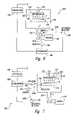
- FIG. 4is a schematic representation of a system 100 for depositing a material onto a micro-device workpiece W in accordance with an embodiment of the invention.
- the system 100includes a reactor 110 having a reaction chamber 120 coupled to a gas supply 130 and a vacuum 140 .
- the reaction chamber 120can have an inlet 122 coupled to the gas supply 130 and an outlet 124 coupled to the vacuum 140 .
- the gas supply 130includes a plurality of gas sources 132 (identified individually as 132 a - c ), a valve assembly 133 , and a plurality of gas lines 136 coupling the gas sources 132 to the valve assembly 133 .
- the gas sources 132can include a first gas source 132 a for providing a first precursor gas “A,” a second gas source 132 b for providing a second precursor gas “B,” and a third gas source 132 c for providing a purge gas “P.”
- the first and second precursors A and Bcan be the constituents that react to form the thin, solid layer on the workpiece W.
- the purge gas Pcan be a type of gas that is compatible with the reaction chamber 120 and the workpiece W.
- the valve assembly 133is coupled to a controller 142 that generates signals for pulsing the individual gases through the reaction chamber 120 in a number of cycles. Each cycle can include a first pulse of the first precursor A, a second pulse of the purge gas P, a third pulse of the second precursor B, and a fourth pulse of the purge gas P. As explained in more detail below, several embodiments of the system 100 monitor and control the pulses of the first precursor A, the second precursor B, and/or the purge gas P to provide consistent results and a high throughput.
- the reactor 110 in the embodiment illustrated in FIG. 4also includes a workpiece support 150 and a gas distributor 160 in the reaction chamber 120 .
- the workpiece support 150can be a plate having a heating element to heat the workpiece W to a desired temperature for catalyzing the reaction between the first precursor A and the second precursor B at the surface of the workpiece W.
- the workpiece support 150may not be heated in all applications.
- the gas distributor 160is coupled to the inlet 122 of the reaction chamber 120 .
- the gas distributor 160has a compartment or plenum 162 and a distributor plate 170 .
- the distributor plate 170has a plurality of passageways 172 through which gasses flow into the reaction chamber 120 along a gas flow F.
- the system 100 shown in FIG. 4also includes a monitoring system that monitors a parameter correlated to a quantity of the first precursor A, the second precursor B, and/or the purge gas P in the gas flow F.
- the monitoring systemfor example, can determine the concentration of the first precursor A, the second precursor B, and/or the purge gas P at different times of the A x -purge-B y -purge pulses in a cycle.
- the data generated by the monitoring systemcan be used to control the pulse length of the first precursor A, the second precursor B, and/or the purge gas P to more consistently produce uniform layers on the workpiece W or increase the throughput of workpieces through the reaction chamber 120 .
- a monitoring system for the system 100includes a radiation source 182 that directs radiation through at least a portion of the gas flow F.
- the radiation source 182can direct a measurement beam 183 a through the reaction chamber 120 at a location between the gas distributor 160 and the workpiece W.
- the radiation source 182can also direct a reference beam 183 b so that it is not affected by the gas flow F flowing through the reaction chamber 120 . It will be appreciated that not all of the embodiments of the radiation source 182 will require a reference beam 183 b .
- the monitoring systemcan also include a primary detector 184 that receives the measurement beam 183 a and a reference detector 186 that receives the reference beam 183 b .
- the primary detector 184generates a first signal corresponding to a parameter of the measurement beam 183 a , such as the intensity of one or more wavelengths of radiation.
- the reference detector 186generates a second signal corresponding to the intensity or another parameter of the reference beam 183 b .
- the primary detector 184 and the reference detector 186are coupled to a comparator 188 that compares the first signal from the primary detector 84 with the second signal from the reference detector 186 .
- the comparator 188then generates a measurement signal based upon the inputs from the primary detector 184 and the reference detector 188 .
- the radiation source 182 and the primary detector 184can be configured to monitor a particular wavelength of radiation that is affected by the presence of a particular gas.
- the radiation source 182can emit a radiation that is absorbed by one of the first precursor A, the second precursor B, or the purge gas P.
- the radiation source 182emits a bandwidth of radiation having a spectrum of wavelengths and the primary detector 184 can include a filter that detects the presence of one or more wavelengths that are affected by the presence of the gases.
- the radiation source 182can generate a sufficiently wide spectrum of radiation to include wavelengths that are affected by each of the first precursor A, the second precursor B, and the purge gas P, the primary detector 184 can accordingly include separate filters that monitor the intensity of the individual wavelengths affected by each of the first precursor A, the second precursor B, and the purge gas P.
- the radiation source 182includes individual emitters that emit specific wavelengths or narrow bandwidths of radiation including a first radiation having a first wavelength affected by the first precursor A, and second radiation having a second wavelength affected by the second precursor B, and a third radiation having a third wavelength affected by the third precursor P. It will be appreciated that several other types of radiation sources and detectors can be used. Suitable radiation sources and detectors are manufactured by INUSA or Online Technologies.
- the monitoring systemprovides real-time data that is correlated to the quantity of the particular constituents in the reaction chamber 120 .
- the primary detector 184measures the change in intensity of the measurement beam 183 a as it changes in correlation to the quantity of the individual gases in the gas flow F.
- the comparator 188uses the first signal from the primary detector 184 to generate a measurement signal that provides an indication of the quantity of the first precursor A, the second precursor B, and/or the purge gas P in the reaction chamber or another portion of the gas flow F.
- the controller 142receives the signals from the comparator 188 and sends control signals to the valve assembly 133 .
- the control signals from the controller 142cause the valve assembly 133 to adjust the pulse length of the purge pulses and/or the precursor pulses.
- the controller 142accordingly contains computer operable instructions, such as software and/or hardware, that carry out embodiments of methods in accordance with the invention for controlling the pulse width of the various gases.
- the computer operable instructionsadjust the pulse width of the purge pulses and/or the precursor pulses based on the measurement signals correlated to the quantity of the first precursor A, the second precursor B, and/or the purge gas P in the gas flow F in real-time during the deposition cycle of a workpiece W.
- the controller 142can accordingly adjust the pulse width for one or more the gases during the deposition cycle to compensate for variances in the processing of an individual workpiece and to increase the throughput of an ALD process.
- FIG. 5is a timing diagram illustrating the individual flows of the first precursor A (labeled as Gas 1 ), the second precursor B (labeled as Gas 2 ), and the purge gas (labeled as Purge Gas) through the valve assembly 133 ( FIG. 4 ).
- the lower three linesshow the on/off configuration of the valve assembly 133 .
- FIG. 5also shows the quantity of the individual gases in the reaction chamber or in the gas flow F downstream from the outlet.
- the upper three linesshow the presence of the individual gases in the reaction chamber relative to the on/off cycling of the valve assembly 133 .
- the quantity of the precursors A and Bfluctuates from zero to a saturation level throughout the cycles.
- the valve assembly 133turns on the flow of the first precursor A shown by line 502 .
- the quantity of the first precursor Aincreases for a ramp time t ramp1 until the quantity or concentration of the first precursor A reaches a desired saturation level.
- the flow of the first precursor A through the valve assembly 133continues for a saturation period t sat1 until a time t 2 .
- the period from t 1 to t 2defines one pulse of the first precursor A.
- the valve assembly 133turns off the flow of the first precursor A (line 502 ) and turns on the flow of the purge gas P (line 504 ).
- the presence of the first precursor Aaccordingly decreases (line 512 ) while the presence of the purge gas P accordingly increases (line 514 ) until a time t 3 defining the endpoint of the purge pulse.
- the valve assembly 133turns off the flow of the purge gas P (line 504 ), and turns on the flow of the second precursor B (line 506 ).
- the presence of the purge gas Pdecreases (line 514 ) while the presence of the second precursor B increases during a ramp time t ramp2 .
- the pulse of the second precursor Bcontinues for a saturation time t sat2 until time t 4 .
- the period from t 3 to t 4defines one pulse of the second precursor B.
- the flow of the second precursor Bis terminated (line 506 ) and the flow of the purge gas P is reinitiated (line 504 ) such that the presence of the second precursor decreases (line 516 ) while the presence of the purge gas P increases (line 514 ) between time t 4 and time t 5 .
- the cycle of pulses from time t 1 to t 5is then repeated for as many cycles as are necessary to form a layer of material having a desired thickness.
- One aspect of certain embodiments of methods in accordance with the inventionis controlling the duration of the precursor pulses for at least one of the first precursor A or the second precursor B.
- the radiation source 182 and the primary detector 184can be configured to detect the concentration of the first precursor A.
- the comparator 188generates measurement signals corresponding to the increase in the concentration of the first precursor A during the ramp time t ramp1 .
- the controller 142can set the duration of the pulse of the first precursor A to continue for an additional time period of t sat1 .
- the time period t sat1can be a predetermined value that is programmed into the controller 142 .
- the saturation period t sat1can be determined using empirical studies. It will be appreciated that the ramp time t ramp1 may vary throughout a run of workpieces because of adsorption/desorption of the precursor in the reaction chamber 120 .
- the controller 142can accordingly set the overall duration of the precursor pulse between time t 1 and t 2 to equal the measured ramp time t ramp1 plus the predetermined saturation time t sat1 .
- a similar processcan be performed for controlling the duration of the pulse of the second precursor B between time t 3 and t 4 by configuring the radiation source 182 and the primary detector 184 to measure the quantity of the second precursor B.
- the system 100can accordingly control the duration of the precursor pulses in real-time during a processing cycle for a workpiece. This is expected to provide more uniform layers on workpieces because it inherently compensates for adsorption and desorption of the precursors. For example, if the precursors are adsorbing to the surfaces of the reaction chamber, the ramp time to bring the concentration of the precursors to a desired level will increase because some molecules of the precursors will be extracted from the gas flow F before reaching the workpiece W.
- the controller 142compensates for adsorption of the precursors by increasing the pulse width in real time according to the measured ramp time.
- the controller 142will indicate a shorter ramp time and a corresponding shorter pulse width. Therefore, the system 100 and methods for controlling the duration of the precursor pulses are expected to provide real-time control of individual pulses of one or more of the precursors in a manner that is expected to produce more uniform layers on the workpieces.
- Another aspect of other embodiments of methods for depositing a layer of material onto a workpieceare directed toward controlling the duration of the purge pulses.
- the radiation source 182 and primary detector 184are configured to detect the presence of the purge gas P.
- the comparator 188sends measurement signals to the controller 142 corresponding to the increase in the purge gas P shown by line 514 of FIG. 5 .
- the controller 142terminates the purge cycle and begins a precursor cycle (e.g., at time t 3 , t 5 and t 7 ).
- the purge cycleis terminated by monitoring the presence of one or more of the precursors.
- the controller 142terminates the purge pulses when the presence of a precursor falls below a desired level or the slope of the lines corresponding to the precursor concentration (e.g., lines 512 and 516 in FIG. 5 ) is at a desired value.
- the pulse widths of the purge pulsescan also be terminated using a combination of the presence of the precursor gas P and the first precursor A or second precursor B.
- the controller 142can accordingly adjust the length of the purge cycles to purge enough of the precursors from the reaction chamber without unnecessarily continuing the duration of the purge pulses. This is expected to provide better control over the deposition process in a manner that is likely to increase throughput and enhance the uniformity of the deposited layers.
- conventional technology for setting the endpoint of purge pulsesinvolves determining a pulse width using empirical studies. This is typically accomplished in conventional systems by starting with long purge times, and then reducing the length of the purge times until an adequate amount of each of the precursors is purged from the reaction chamber.
- the system 100is expected to resolve these problems because the pulse width of the purge pulses are controlled in real-time to reduce the duration of the purge pulses in a manner that compensates for both adsorption and desorption during a run of workpieces. Therefore, several embodiments of methods for operating the system 100 are useful for enhancing the throughput of workpieces and the uniformity of deposited layers.
- FIGS. 6-8are schematic diagrams illustrating additional embodiments of systems in accordance with the invention. Like reference numbers refer to like components in FIGS. 4 and 6 - 8 .
- FIG. 6illustrates a system 600 in which the monitoring system includes a radiation source 182 that directs a measurement beam 183 a through a gas flow F in the outlet 124 .
- the primary detector 184can be positioned on another side of the outlet 124 .
- FIG. 7illustrates a system 700 in which the monitoring system further includes a reflector 185 located just downstream from the workpiece W.
- the reflector 185can be a mirror or another type of device that does not alter the measurement beam 183 a other than to change its direction.
- the reflector 185for example, can be mounted to the workpiece support 150 .
- FIG. 8illustrates a system 800 in which the radiation source 182 is mounted to the workpiece holder 150 in the reaction chamber 120 .
- the radiation source 182 in the system 800directs the measurement beam 183 a to the primary detector 184 .
- the monitoring systemdoes not include a reference detector 186 or a comparator 188 .
- the detector 184sends a measurement signal directly to the controller 142 .
- the controller 142can include the hardware for receiving and processing the measurement signal from the detector 184 .
Landscapes
- Chemical & Material Sciences (AREA)
- General Chemical & Material Sciences (AREA)
- Chemical Kinetics & Catalysis (AREA)
- Engineering & Computer Science (AREA)
- Materials Engineering (AREA)
- Mechanical Engineering (AREA)
- Metallurgy (AREA)
- Organic Chemistry (AREA)
- Chemical Vapour Deposition (AREA)
Abstract
Description
Claims (21)
Priority Applications (1)
| Application Number | Priority Date | Filing Date | Title |
|---|---|---|---|
| US11/027,809US7481887B2 (en) | 2002-05-24 | 2004-12-29 | Apparatus for controlling gas pulsing in processes for depositing materials onto micro-device workpieces |
Applications Claiming Priority (2)
| Application Number | Priority Date | Filing Date | Title |
|---|---|---|---|
| US10/155,547US6838114B2 (en) | 2002-05-24 | 2002-05-24 | Methods for controlling gas pulsing in processes for depositing materials onto micro-device workpieces |
| US11/027,809US7481887B2 (en) | 2002-05-24 | 2004-12-29 | Apparatus for controlling gas pulsing in processes for depositing materials onto micro-device workpieces |
Related Parent Applications (1)
| Application Number | Title | Priority Date | Filing Date |
|---|---|---|---|
| US10/155,547DivisionUS6838114B2 (en) | 2002-05-24 | 2002-05-24 | Methods for controlling gas pulsing in processes for depositing materials onto micro-device workpieces |
Publications (2)
| Publication Number | Publication Date |
|---|---|
| US20050120954A1 US20050120954A1 (en) | 2005-06-09 |
| US7481887B2true US7481887B2 (en) | 2009-01-27 |
Family
ID=29549093
Family Applications (2)
| Application Number | Title | Priority Date | Filing Date |
|---|---|---|---|
| US10/155,547Expired - Fee RelatedUS6838114B2 (en) | 2002-05-24 | 2002-05-24 | Methods for controlling gas pulsing in processes for depositing materials onto micro-device workpieces |
| US11/027,809Expired - Fee RelatedUS7481887B2 (en) | 2002-05-24 | 2004-12-29 | Apparatus for controlling gas pulsing in processes for depositing materials onto micro-device workpieces |
Family Applications Before (1)
| Application Number | Title | Priority Date | Filing Date |
|---|---|---|---|
| US10/155,547Expired - Fee RelatedUS6838114B2 (en) | 2002-05-24 | 2002-05-24 | Methods for controlling gas pulsing in processes for depositing materials onto micro-device workpieces |
Country Status (1)
| Country | Link |
|---|---|
| US (2) | US6838114B2 (en) |
Cited By (3)
| Publication number | Priority date | Publication date | Assignee | Title |
|---|---|---|---|---|
| US20090064932A1 (en)* | 2007-08-31 | 2009-03-12 | Samsung Electronics Co., Ltd. | Apparatus for HDP-CVD and method of forming insulating layer using the same |
| US20120240348A1 (en)* | 2002-03-28 | 2012-09-27 | Kazuyuki Okuda | Substrate processing apparatus |
| US10526700B2 (en)* | 2014-12-19 | 2020-01-07 | Lam Research Corporation | Hardware and process for film uniformity improvement |
Families Citing this family (45)
| Publication number | Priority date | Publication date | Assignee | Title |
|---|---|---|---|---|
| DE10003758A1 (en)* | 2000-01-28 | 2001-08-02 | Aixtron Gmbh | Device and method for separating at least one precursor present in liquid or dissolved form |
| US6670071B2 (en)* | 2002-01-15 | 2003-12-30 | Quallion Llc | Electric storage battery construction and method of manufacture |
| US7439191B2 (en)* | 2002-04-05 | 2008-10-21 | Applied Materials, Inc. | Deposition of silicon layers for active matrix liquid crystal display (AMLCD) applications |
| US6838114B2 (en)* | 2002-05-24 | 2005-01-04 | Micron Technology, Inc. | Methods for controlling gas pulsing in processes for depositing materials onto micro-device workpieces |
| US6821347B2 (en) | 2002-07-08 | 2004-11-23 | Micron Technology, Inc. | Apparatus and method for depositing materials onto microelectronic workpieces |
| US6746460B2 (en) | 2002-08-07 | 2004-06-08 | Satiety, Inc. | Intra-gastric fastening devices |
| US6955725B2 (en)* | 2002-08-15 | 2005-10-18 | Micron Technology, Inc. | Reactors with isolated gas connectors and methods for depositing materials onto micro-device workpieces |
| US6926775B2 (en)* | 2003-02-11 | 2005-08-09 | Micron Technology, Inc. | Reactors with isolated gas connectors and methods for depositing materials onto micro-device workpieces |
| US7335396B2 (en)* | 2003-04-24 | 2008-02-26 | Micron Technology, Inc. | Methods for controlling mass flow rates and pressures in passageways coupled to reaction chambers and systems for depositing material onto microfeature workpieces in reaction chambers |
| US7235138B2 (en) | 2003-08-21 | 2007-06-26 | Micron Technology, Inc. | Microfeature workpiece processing apparatus and methods for batch deposition of materials on microfeature workpieces |
| US7344755B2 (en)* | 2003-08-21 | 2008-03-18 | Micron Technology, Inc. | Methods and apparatus for processing microfeature workpieces; methods for conditioning ALD reaction chambers |
| US7422635B2 (en)* | 2003-08-28 | 2008-09-09 | Micron Technology, Inc. | Methods and apparatus for processing microfeature workpieces, e.g., for depositing materials on microfeature workpieces |
| US7056806B2 (en) | 2003-09-17 | 2006-06-06 | Micron Technology, Inc. | Microfeature workpiece processing apparatus and methods for controlling deposition of materials on microfeature workpieces |
| US7282239B2 (en) | 2003-09-18 | 2007-10-16 | Micron Technology, Inc. | Systems and methods for depositing material onto microfeature workpieces in reaction chambers |
| US7323231B2 (en)* | 2003-10-09 | 2008-01-29 | Micron Technology, Inc. | Apparatus and methods for plasma vapor deposition processes |
| US7581511B2 (en) | 2003-10-10 | 2009-09-01 | Micron Technology, Inc. | Apparatus and methods for manufacturing microfeatures on workpieces using plasma vapor processes |
| US7311947B2 (en)* | 2003-10-10 | 2007-12-25 | Micron Technology, Inc. | Laser assisted material deposition |
| US7647886B2 (en)* | 2003-10-15 | 2010-01-19 | Micron Technology, Inc. | Systems for depositing material onto workpieces in reaction chambers and methods for removing byproducts from reaction chambers |
| US7258892B2 (en)* | 2003-12-10 | 2007-08-21 | Micron Technology, Inc. | Methods and systems for controlling temperature during microfeature workpiece processing, e.g., CVD deposition |
| US7906393B2 (en) | 2004-01-28 | 2011-03-15 | Micron Technology, Inc. | Methods for forming small-scale capacitor structures |
| US7115304B2 (en)* | 2004-02-19 | 2006-10-03 | Nanosolar, Inc. | High throughput surface treatment on coiled flexible substrates |
| US7584942B2 (en) | 2004-03-31 | 2009-09-08 | Micron Technology, Inc. | Ampoules for producing a reaction gas and systems for depositing materials onto microfeature workpieces in reaction chambers |
| US20050249873A1 (en)* | 2004-05-05 | 2005-11-10 | Demetrius Sarigiannis | Apparatuses and methods for producing chemically reactive vapors used in manufacturing microelectronic devices |
| US8133554B2 (en) | 2004-05-06 | 2012-03-13 | Micron Technology, Inc. | Methods for depositing material onto microfeature workpieces in reaction chambers and systems for depositing materials onto microfeature workpieces |
| US7699932B2 (en)* | 2004-06-02 | 2010-04-20 | Micron Technology, Inc. | Reactors, systems and methods for depositing thin films onto microfeature workpieces |
| US20050287806A1 (en)* | 2004-06-24 | 2005-12-29 | Hiroyuki Matsuura | Vertical CVD apparatus and CVD method using the same |
| US20060093746A1 (en)* | 2004-11-04 | 2006-05-04 | Tokyo Electron Limited | Method and apparatus for atomic layer deposition |
| US20060165873A1 (en)* | 2005-01-25 | 2006-07-27 | Micron Technology, Inc. | Plasma detection and associated systems and methods for controlling microfeature workpiece deposition processes |
| US7459175B2 (en)* | 2005-01-26 | 2008-12-02 | Tokyo Electron Limited | Method for monolayer deposition |
| JP2006253696A (en)* | 2005-03-10 | 2006-09-21 | Asm America Inc | Gas injector control system |
| US20060237138A1 (en)* | 2005-04-26 | 2006-10-26 | Micron Technology, Inc. | Apparatuses and methods for supporting microelectronic devices during plasma-based fabrication processes |
| US7735452B2 (en)* | 2005-07-08 | 2010-06-15 | Mks Instruments, Inc. | Sensor for pulsed deposition monitoring and control |
| US7807062B2 (en)* | 2006-07-10 | 2010-10-05 | Micron Technology, Inc. | Electron induced chemical etching and deposition for local circuit repair |
| US7892978B2 (en)* | 2006-07-10 | 2011-02-22 | Micron Technology, Inc. | Electron induced chemical etching for device level diagnosis |
| US7791055B2 (en) | 2006-07-10 | 2010-09-07 | Micron Technology, Inc. | Electron induced chemical etching/deposition for enhanced detection of surface defects |
| US7718080B2 (en)* | 2006-08-14 | 2010-05-18 | Micron Technology, Inc. | Electronic beam processing device and method using carbon nanotube emitter |
| US7833427B2 (en) | 2006-08-14 | 2010-11-16 | Micron Technology, Inc. | Electron beam etching device and method |
| US7791071B2 (en) | 2006-08-14 | 2010-09-07 | Micron Technology, Inc. | Profiling solid state samples |
| FI122749B (en)* | 2007-12-20 | 2012-06-29 | Beneq Oy | coating System |
| US7989360B2 (en) | 2008-01-07 | 2011-08-02 | Micron Technology, Inc. | Semiconductor processing methods, and methods for forming silicon dioxide |
| US20100112191A1 (en)* | 2008-10-30 | 2010-05-06 | Micron Technology, Inc. | Systems and associated methods for depositing materials |
| JP5902896B2 (en)* | 2011-07-08 | 2016-04-13 | 東京エレクトロン株式会社 | Substrate processing equipment |
| KR102040758B1 (en)* | 2011-08-05 | 2019-11-05 | 쓰리엠 이노베이티브 프로퍼티즈 캄파니 | Systems and methods for processing vapor |
| DE102022134331A1 (en)* | 2022-12-21 | 2024-06-27 | Aixtron Se | Procedure for preventing incorrect operation of a CVD reactor |
| WO2025106690A1 (en)* | 2023-11-15 | 2025-05-22 | Lam Research Corporation | Precursor concentration monitoring |
Citations (426)
| Publication number | Priority date | Publication date | Assignee | Title |
|---|---|---|---|---|
| US579269A (en) | 1897-03-23 | Roller-bearing | ||
| US2508500A (en) | 1942-05-23 | 1950-05-23 | Hartford Nat Bank & Trust Co | Apparatus for applying metal coatings on insulators |
| GB1065762A (en) | 1963-01-16 | 1967-04-19 | Ass Elect Ind | Improvements relating to electroluminescent devices |
| US3522836A (en) | 1966-07-06 | 1970-08-04 | Battelle Development Corp | Method of manufacturing wire and the like |
| US3618919A (en) | 1969-11-03 | 1971-11-09 | Btu Eng Corp | Adjustable heat and gas barrier |
| US3620934A (en) | 1966-08-08 | 1971-11-16 | Fer Blanc Sarl Centre Rech Du | Method of electrolytic tinning sheet steel |
| US3630769A (en) | 1968-04-24 | 1971-12-28 | Plessey Co Ltd | PRODUCTION OF VAPOR-DEPOSITED Nb{11 B{11 Sn CONDUCTOR MATERIAL |
| US3630881A (en) | 1970-01-22 | 1971-12-28 | Ibm | Cathode-target assembly for rf sputtering apparatus |
| US3634212A (en) | 1970-05-06 | 1972-01-11 | M & T Chemicals Inc | Electrodeposition of bright acid tin and electrolytes therefor |
| GB1469230A (en) | 1974-06-04 | 1977-04-06 | Secr Defence | Preparation of chemical c-mpounds |
| US4018949A (en) | 1976-01-12 | 1977-04-19 | Ford Motor Company | Selective tin deposition onto aluminum piston skirt areas |
| SU598630A1 (en) | 1974-08-15 | 1978-02-21 | Предприятие П/Я Р-6707 | Device for introducing into reaction chamber |
| US4098923A (en) | 1976-06-07 | 1978-07-04 | Motorola, Inc. | Pyrolytic deposition of silicon dioxide on semiconductors using a shrouded boat |
| US4242370A (en) | 1978-03-17 | 1980-12-30 | Abdalla Mohamed I | Method of manufacturing thin film electroluminescent devices |
| US4242182A (en) | 1978-07-21 | 1980-12-30 | Francine Popescu | Bright tin electroplating bath |
| US4269625A (en) | 1978-12-04 | 1981-05-26 | U.S. Philips Corporation | Bath for electroless depositing tin on substrates |
| US4289061A (en) | 1977-10-03 | 1981-09-15 | Hooker Chemicals & Plastics Corp. | Device and assembly for mounting parts |
| US4313783A (en) | 1980-05-19 | 1982-02-02 | Branson International Plasma Corporation | Computer controlled system for processing semiconductor wafers |
| US4388342A (en)* | 1979-05-29 | 1983-06-14 | Hitachi, Ltd. | Method for chemical vapor deposition |
| US4397753A (en) | 1982-09-20 | 1983-08-09 | Circuit Chemistry Corporation | Solder stripping solution |
| US4436674A (en) | 1981-07-30 | 1984-03-13 | J.C. Schumacher Co. | Vapor mass flow control system |
| US4438724A (en) | 1982-08-13 | 1984-03-27 | Energy Conversion Devices, Inc. | Grooved gas gate |
| US4469801A (en) | 1980-09-04 | 1984-09-04 | Toshio Hirai | Titanium-containing silicon nitride film bodies and a method of producing the same |
| US4509456A (en) | 1981-07-28 | 1985-04-09 | Veb Zentrum Fur Forschung Und Technologie Mikroelektronik | Apparatus for guiding gas for LP CVD processes in a tube reactor |
| US4545136A (en) | 1981-03-16 | 1985-10-08 | Sovonics Solar Systems | Isolation valve |
| US4590042A (en) | 1984-12-24 | 1986-05-20 | Tegal Corporation | Plasma reactor having slotted manifold |
| US4593644A (en) | 1983-10-26 | 1986-06-10 | Rca Corporation | Continuous in-line deposition system |
| JPS61292894A (en) | 1985-06-19 | 1986-12-23 | 富士通株式会社 | Dual source deposition method |
| US4681777A (en) | 1986-05-05 | 1987-07-21 | Engelken Robert D | Method for electroless and vapor deposition of thin films of three tin sulfide phases on conductive and nonconductive substrates |
| EP0140246B1 (en) | 1983-10-11 | 1987-09-16 | GTE Products Corporation | A thin film electroluminescent display device |
| JPS62235728A (en) | 1986-04-07 | 1987-10-15 | Nec Corp | Vapor phase epitaxial growth device |
| JPS62263629A (en) | 1986-05-12 | 1987-11-16 | Hitachi Ltd | Vapor phase growth equipment |
| US4738295A (en) | 1985-04-02 | 1988-04-19 | Genser Hans G | Method and apparatus for evaporating a fluid in a rotating vacuum evaporation system |
| JPS6320490Y2 (en) | 1979-09-08 | 1988-06-07 | ||
| JPS63111177U (en) | 1987-01-12 | 1988-07-16 | ||
| JPS63234198A (en) | 1987-03-24 | 1988-09-29 | 株式会社東芝 | Flange image leakage detection device |
| JPS63256460A (en) | 1987-04-14 | 1988-10-24 | Oki Electric Ind Co Ltd | Substrate for thermal head and production thereof |
| US4780178A (en) | 1982-10-15 | 1988-10-25 | Yamoto Scientific Co. Ltd. | Rotary evaporator with control system |
| US4826579A (en) | 1982-06-25 | 1989-05-02 | Cel Systems Corporation | Electrolytic preparation of tin and other metals |
| US4832115A (en) | 1986-07-09 | 1989-05-23 | Albers Technologies Corporation | Method and apparatus for simultaneous heat and mass transfer |
| US4871417A (en) | 1986-07-04 | 1989-10-03 | Dainippon Screen Mfg. Co., Ltd. | Method and apparatus for surface treating of substrates |
| JPH01273991A (en) | 1988-04-26 | 1989-11-01 | Ishikawajima Harima Heavy Ind Co Ltd | Furnace sealing device |
| US4894132A (en)* | 1987-10-21 | 1990-01-16 | Mitsubishi Denki Kabushiki Kaisha | Sputtering method and apparatus |
| US4911638A (en) | 1989-05-18 | 1990-03-27 | Direction Incorporated | Controlled diffusion environment capsule and system |
| US4923715A (en) | 1986-03-31 | 1990-05-08 | Kabushiki Kaisha Toshiba | Method of forming thin film by chemical vapor deposition |
| US4948979A (en) | 1987-12-21 | 1990-08-14 | Kabushiki Kaisha Toshiba | Vacuum device for handling workpieces |
| US4949669A (en) | 1988-12-20 | 1990-08-21 | Texas Instruments Incorporated | Gas flow systems in CCVD reactors |
| US4966646A (en) | 1986-09-24 | 1990-10-30 | Board Of Trustees Of Leland Stanford University | Method of making an integrated, microminiature electric-to-fluidic valve |
| US4977106A (en) | 1990-05-01 | 1990-12-11 | Texas Instruments Incorporated | Tin chemical vapor deposition using TiCl4 and SiH4 |
| US5015330A (en) | 1989-02-28 | 1991-05-14 | Kabushiki Kaisha Toshiba | Film forming method and film forming device |
| US5017404A (en) | 1988-09-06 | 1991-05-21 | Schott Glaswerke | Plasma CVD process using a plurality of overlapping plasma columns |
| US5020476A (en) | 1990-04-17 | 1991-06-04 | Ds Research, Inc. | Distributed source assembly |
| JPH03174717A (en) | 1989-10-06 | 1991-07-29 | Nippon Kentetsu Co Ltd | Method of supplying water of plasma ashing |
| US5043614A (en) | 1990-02-02 | 1991-08-27 | Ford Motor Company | Alternator rectifier bridge assembly |
| US5062446A (en) | 1991-01-07 | 1991-11-05 | Sematech, Inc. | Intelligent mass flow controller |
| US5076205A (en) | 1989-01-06 | 1991-12-31 | General Signal Corporation | Modular vapor processor system |
| US5091207A (en) | 1989-07-20 | 1992-02-25 | Fujitsu Limited | Process and apparatus for chemical vapor deposition |
| US5090985A (en) | 1989-10-17 | 1992-02-25 | Libbey-Owens-Ford Co. | Method for preparing vaporized reactants for chemical vapor deposition |
| JPH04100533A (en) | 1990-08-18 | 1992-04-02 | Mitsubishi Electric Corp | vacuum container |
| US5131752A (en) | 1990-06-28 | 1992-07-21 | Tamarack Scientific Co., Inc. | Method for film thickness endpoint control |
| JPH04213818A (en) | 1990-12-07 | 1992-08-04 | Sony Corp | Cvd device |
| US5136975A (en) | 1990-06-21 | 1992-08-11 | Watkins-Johnson Company | Injector and method for delivering gaseous chemicals to a surface |
| US5172849A (en) | 1991-09-25 | 1992-12-22 | General Motors Corporation | Method and apparatus for convection brazing of aluminum heat exchangers |
| US5200023A (en) | 1991-08-30 | 1993-04-06 | International Business Machines Corp. | Infrared thermographic method and apparatus for etch process monitoring and control |
| US5223113A (en) | 1990-07-20 | 1993-06-29 | Tokyo Electron Limited | Apparatus for forming reduced pressure and for processing object |
| US5232749A (en) | 1991-04-30 | 1993-08-03 | Micron Technology, Inc. | Formation of self-limiting films by photoemission induced vapor deposition |
| US5248527A (en) | 1991-03-01 | 1993-09-28 | C. Uyemura And Company, Limited | Process for electroless plating tin, lead or tin-lead alloy |
| US5286296A (en) | 1991-01-10 | 1994-02-15 | Sony Corporation | Multi-chamber wafer process equipment having plural, physically communicating transfer means |
| JPH06151558A (en) | 1992-11-09 | 1994-05-31 | Tokyo Electron Ltd | Transfer processing device |
| US5325020A (en) | 1990-09-28 | 1994-06-28 | Abtox, Inc. | Circular waveguide plasma microwave sterilizer apparatus |
| JPH06201539A (en) | 1993-01-04 | 1994-07-19 | Yasuo Kitsuta | Centrifugal evaporator |
| JPH06202372A (en) | 1992-10-21 | 1994-07-22 | Hewlett Packard Co <Hp> | Toner composition and its adjusting method |
| US5364219A (en) | 1991-06-24 | 1994-11-15 | Tdk Corporation | Apparatus for clean transfer of objects |
| US5366557A (en) | 1990-06-18 | 1994-11-22 | At&T Bell Laboratories | Method and apparatus for forming integrated circuit layers |
| JPH06342785A (en) | 1993-06-01 | 1994-12-13 | Fujitsu Ltd | Exhauster of vapor growth device and cleaning method thereof |
| US5372837A (en) | 1990-05-30 | 1994-12-13 | Sharp Kabushiki Kaisha | Method of manufacturing thin film EL device utilizing a shutter |
| US5377429A (en) | 1993-04-19 | 1995-01-03 | Micron Semiconductor, Inc. | Method and appartus for subliming precursors |
| US5380396A (en) | 1991-05-30 | 1995-01-10 | Hitachi, Ltd. | Valve and semiconductor fabricating equipment using the same |
| US5409129A (en) | 1990-12-28 | 1995-04-25 | Hokkai Can Co., Ltd. | Welded cans |
| US5418180A (en) | 1994-06-14 | 1995-05-23 | Micron Semiconductor, Inc. | Process for fabricating storage capacitor structures using CVD tin on hemispherical grain silicon |
| US5427666A (en) | 1993-09-09 | 1995-06-27 | Applied Materials, Inc. | Method for in-situ cleaning a Ti target in a Ti + TiN coating process |
| US5432015A (en) | 1992-05-08 | 1995-07-11 | Westaim Technologies, Inc. | Electroluminescent laminate with thick film dielectric |
| US5433835A (en) | 1993-11-24 | 1995-07-18 | Applied Materials, Inc. | Sputtering device and target with cover to hold cooling fluid |
| US5433787A (en) | 1991-12-12 | 1995-07-18 | Canon Kabushiki Kaisha | Apparatus for forming deposited film including light transmissive diffusion plate |
| US5445491A (en) | 1991-08-27 | 1995-08-29 | Toshiba Kikai Kabushiki Kaisha | Method for multichamber sheet-after-sheet type treatment |
| US5453124A (en) | 1992-12-30 | 1995-09-26 | Texas Instruments Incorporated | Programmable multizone gas injector for single-wafer semiconductor processing equipment |
| US5474612A (en) | 1990-03-19 | 1995-12-12 | Kabushiki Kaisha Toshiba | Vapor-phase deposition apparatus and vapor-phase deposition method |
| US5477623A (en) | 1992-11-25 | 1995-12-26 | Matsushita Electric Industrial Co., Ltd. | Drying apparatus |
| US5480818A (en) | 1992-02-10 | 1996-01-02 | Fujitsu Limited | Method for forming a film and method for manufacturing a thin film transistor |
| US5496410A (en) | 1992-03-10 | 1996-03-05 | Hitachi, Ltd. | Plasma processing apparatus and method of processing substrates by using same apparatus |
| US5498292A (en) | 1994-06-16 | 1996-03-12 | Kishimoto Sangyo Co., Ltd. | Heating device used for a gas phase growing mechanism or heat treatment mechanism |
| US5500256A (en) | 1994-08-16 | 1996-03-19 | Fujitsu Limited | Dry process apparatus using plural kinds of gas |
| JPH0834678B2 (en) | 1986-08-20 | 1996-03-29 | 日新電機株式会社 | Instantaneous voltage drop compensator |
| US5505986A (en) | 1994-02-14 | 1996-04-09 | Planar Systems, Inc. | Multi-source reactive deposition process for the preparation of blue light emitting phosphor layers for AC TFEL devices |
| US5522934A (en) | 1994-04-26 | 1996-06-04 | Tokyo Electron Limited | Plasma processing apparatus using vertical gas inlets one on top of another |
| US5532190A (en) | 1994-05-26 | 1996-07-02 | U.S. Philips Corporation | Plasma treatment method in electronic device manufacture |
| US5536317A (en) | 1995-10-27 | 1996-07-16 | Specialty Coating Systems, Inc. | Parylene deposition apparatus including a quartz crystal thickness/rate controller |
| US5562800A (en) | 1993-09-20 | 1996-10-08 | Hitachi, Ltd. | Wafer transport method |
| US5575883A (en) | 1993-07-09 | 1996-11-19 | Fujitsu Limited | Apparatus and process for fabricating semiconductor devices |
| US5589002A (en) | 1994-03-24 | 1996-12-31 | Applied Materials, Inc. | Gas distribution plate for semiconductor wafer processing apparatus with means for inhibiting arcing |
| US5589110A (en) | 1992-11-20 | 1996-12-31 | Mitsubishi Electric Corp | Container for liquid metal organic compound |
| US5592581A (en) | 1993-07-19 | 1997-01-07 | Tokyo Electron Kabushiki Kaisha | Heat treatment apparatus |
| US5595606A (en) | 1995-04-20 | 1997-01-21 | Tokyo Electron Limited | Shower head and film forming apparatus using the same |
| US5599513A (en) | 1989-11-13 | 1997-02-04 | Showa Denko K.K. | Gas distribution plate for use with fluidized-bed gas-phase polymerizer |
| JPH0982650A (en) | 1995-09-14 | 1997-03-28 | Kokusai Electric Co Ltd | Semiconductor manufacturing equipment |
| US5624498A (en) | 1993-12-22 | 1997-04-29 | Samsung Electronics Co., Ltd. | Showerhead for a gas supplying apparatus |
| US5626936A (en) | 1993-09-09 | 1997-05-06 | Energy Pillow, Inc. | Phase change insulation system |
| US5640751A (en) | 1995-07-17 | 1997-06-24 | Thermionics Laboratories, Inc. | Vacuum flange |
| US5643394A (en) | 1994-09-16 | 1997-07-01 | Applied Materials, Inc. | Gas injection slit nozzle for a plasma process reactor |
| US5654589A (en) | 1995-06-06 | 1997-08-05 | Advanced Micro Devices, Incorporated | Landing pad technology doubled up as local interconnect and borderless contact for deep sub-half micrometer IC application |
| US5683538A (en)* | 1994-12-23 | 1997-11-04 | International Business Machines Corporation | Control of etch selectivity |
| US5693288A (en) | 1994-06-24 | 1997-12-02 | Nisshin Steel Co., Ltd. | Seal assembly for thermal treatment furnaces using an atmospheric gas containing hydrogen gas |
| JPH108255A (en) | 1996-06-20 | 1998-01-13 | Ebara Corp | Liquid raw material vaporizing device |
| US5716796A (en) | 1990-01-23 | 1998-02-10 | Medical Devices Corporation | Optical blood hemostatic analysis apparatus and method |
| US5729896A (en) | 1996-10-31 | 1998-03-24 | International Business Machines Corporation | Method for attaching a flip chip on flexible circuit carrier using chip with metallic cap on solder |
| US5733375A (en) | 1995-01-06 | 1998-03-31 | Tokyo Electron Limited | Apparatus for supplying a treatment material |
| US5746434A (en) | 1996-07-09 | 1998-05-05 | Lam Research Corporation | Chamber interfacing O-rings and method for implementing same |
| US5754297A (en)* | 1994-01-28 | 1998-05-19 | Applied Materials, Inc. | Method and apparatus for monitoring the deposition rate of films during physical vapor deposition |
| US5766364A (en) | 1996-07-17 | 1998-06-16 | Matsushita Electric Industrial Co., Ltd. | Plasma processing apparatus |
| US5769950A (en) | 1985-07-23 | 1998-06-23 | Canon Kabushiki Kaisha | Device for forming deposited film |
| US5769952A (en) | 1994-06-07 | 1998-06-23 | Tokyo Electron, Ltd. | Reduced pressure and normal pressure treatment apparatus |
| US5773085A (en) | 1994-07-04 | 1998-06-30 | Nippon Hoso Kyokai | Method of manufacturing ternary compound thin films |
| US5772771A (en) | 1995-12-13 | 1998-06-30 | Applied Materials, Inc. | Deposition chamber for improved deposition thickness uniformity |
| US5788778A (en) | 1996-09-16 | 1998-08-04 | Applied Komatsu Technology, Inc. | Deposition chamber cleaning technique using a high power remote excitation source |
| US5792700A (en) | 1996-05-31 | 1998-08-11 | Micron Technology, Inc. | Semiconductor processing method for providing large grain polysilicon films |
| US5792269A (en) | 1995-10-31 | 1998-08-11 | Applied Materials, Inc. | Gas distribution for CVD systems |
| JPH10223719A (en) | 1996-12-06 | 1998-08-21 | Dainippon Screen Mfg Co Ltd | Substrate carrier system, substrate processor and substrate carrier method |
| WO1998037258A1 (en) | 1997-02-25 | 1998-08-27 | Moore Epitaxial Inc. | A rapid thermal processing barrel reactor for processing substrates |
| US5803938A (en) | 1992-09-21 | 1998-09-08 | Mitsubishi Denki Kabushiki Kaisha | Liquid vaporizing apparatus |
| US5819683A (en) | 1995-05-02 | 1998-10-13 | Tokyo Electron Limited | Trap apparatus |
| US5820686A (en) | 1993-01-21 | 1998-10-13 | Moore Epitaxial, Inc. | Multi-layer susceptor for rapid thermal process reactors |
| US5820641A (en) | 1996-02-09 | 1998-10-13 | Mks Instruments, Inc. | Fluid cooled trap |
| US5827370A (en) | 1997-01-13 | 1998-10-27 | Mks Instruments, Inc. | Method and apparatus for reducing build-up of material on inner surface of tube downstream from a reaction furnace |
| US5833888A (en) | 1996-12-31 | 1998-11-10 | Atmi Ecosys Corporation | Weeping weir gas/liquid interface structure |
| US5846330A (en) | 1997-06-26 | 1998-12-08 | Celestech, Inc. | Gas injection disc assembly for CVD applications |
| US5846275A (en) | 1996-12-31 | 1998-12-08 | Atmi Ecosys Corporation | Clog-resistant entry structure for introducing a particulate solids-containing and/or solids-forming gas stream to a gas processing system |
| US5851294A (en) | 1995-10-23 | 1998-12-22 | Watkins-Johnson Company | Gas injection system for semiconductor processing |
| US5851849A (en) | 1997-05-22 | 1998-12-22 | Lucent Technologies Inc. | Process for passivating semiconductor laser structures with severe steps in surface topography |
| US5865417A (en) | 1996-09-27 | 1999-02-02 | Redwood Microsystems, Inc. | Integrated electrically operable normally closed valve |
| US5866986A (en) | 1996-08-05 | 1999-02-02 | Integrated Electronic Innovations, Inc. | Microwave gas phase plasma source |
| US5865887A (en) | 1996-09-13 | 1999-02-02 | Seh America, Inc. | Method for improving mechanical strength of the neck section of czochralski silicon crystal |
| US5868159A (en) | 1996-07-12 | 1999-02-09 | Mks Instruments, Inc. | Pressure-based mass flow controller |
| WO1999006610A1 (en) | 1997-08-01 | 1999-02-11 | Applied Komatsu Technology, Inc. | Method and apparatus for detecting the endpoint of a chamber cleaning |
| US5879459A (en) | 1997-08-29 | 1999-03-09 | Genus, Inc. | Vertically-stacked process reactor and cluster tool system for atomic layer deposition |
| US5879516A (en) | 1996-02-29 | 1999-03-09 | Kasman; David H. | Kugelrohr or distillation apparatus |
| US5885425A (en) | 1995-06-06 | 1999-03-23 | International Business Machines Corporation | Method for selective material deposition on one side of raised or recessed features |
| US5895530A (en) | 1996-02-26 | 1999-04-20 | Applied Materials, Inc. | Method and apparatus for directing fluid through a semiconductor processing chamber |
| US5902403A (en) | 1995-11-28 | 1999-05-11 | Applied Materials, Inc. | Method and apparatus for cleaning a chamber |
| US5908947A (en) | 1996-02-09 | 1999-06-01 | Micron Technology, Inc. | Difunctional amino precursors for the deposition of films comprising metals |
| US5911238A (en) | 1996-10-04 | 1999-06-15 | Emerson Electric Co. | Thermal mass flowmeter and mass flow controller, flowmetering system and method |
| JPH11172438A (en) | 1997-09-29 | 1999-06-29 | Samsung Electron Co Ltd | Method for forming metal nitride film by chemical vapor deposition and method for forming metal contact of semiconductor device using the same |
| US5932286A (en) | 1993-03-16 | 1999-08-03 | Applied Materials, Inc. | Deposition of silicon nitride thin films |
| US5936829A (en) | 1997-01-02 | 1999-08-10 | Cvc Products, Inc. | Thermally conductive chuck for vacuum processor |
| US5940684A (en) | 1996-05-23 | 1999-08-17 | Rohm, Co., Ltd. | Method and equipment for manufacturing semiconductor device |
| US5953634A (en) | 1995-02-13 | 1999-09-14 | Kabushiki Kaisha Toshiba | Method of manufacturing semiconductor device |
| US5956613A (en) | 1995-12-27 | 1999-09-21 | Lsi Logic Corporation | Method for improvement of TiN CVD film quality |
| US5958140A (en) | 1995-07-27 | 1999-09-28 | Tokyo Electron Limited | One-by-one type heat-processing apparatus |
| US5961775A (en) | 1987-08-19 | 1999-10-05 | Fujitsu Limited | Apparatus for removing organic resist from semiconductor |
| US5963336A (en)* | 1995-10-10 | 1999-10-05 | American Air Liquide Inc. | Chamber effluent monitoring system and semiconductor processing system comprising absorption spectroscopy measurement system, and methods of use |
| US5968587A (en) | 1996-11-13 | 1999-10-19 | Applied Materials, Inc. | Systems and methods for controlling the temperature of a vapor deposition apparatus |
| US5972430A (en) | 1997-11-26 | 1999-10-26 | Advanced Technology Materials, Inc. | Digital chemical vapor deposition (CVD) method for forming a multi-component oxide layer |
| US5994181A (en) | 1997-05-19 | 1999-11-30 | United Microelectronics Corp. | Method for forming a DRAM cell electrode |
| US5998932A (en) | 1998-06-26 | 1999-12-07 | Lam Research Corporation | Focus ring arrangement for substantially eliminating unconfined plasma in a plasma processing chamber |
| US5997588A (en) | 1995-10-13 | 1999-12-07 | Advanced Semiconductor Materials America, Inc. | Semiconductor processing system with gas curtain |
| US6006694A (en) | 1997-12-05 | 1999-12-28 | Tegal Corporation | Plasma reactor with a deposition shield |
| US6008086A (en) | 1995-10-24 | 1999-12-28 | Micron Technology, Inc. | Method of deposting uniform dielectric film deposition on textured surfaces |
| US6016611A (en) | 1998-07-13 | 2000-01-25 | Applied Komatsu Technology, Inc. | Gas flow control in a substrate processing system |
| US6022483A (en) | 1998-03-10 | 2000-02-08 | Intergrated Systems, Inc. | System and method for controlling pressure |
| US6032923A (en) | 1998-01-08 | 2000-03-07 | Xerox Corporation | Fluid valves having cantilevered blocking films |
| US6039557A (en) | 1989-12-22 | 2000-03-21 | Imarx Pharmaceutical Corp. | Apparatus for making gas-filled vesicles of optimal size |
| US6042652A (en) | 1999-05-01 | 2000-03-28 | P.K. Ltd | Atomic layer deposition apparatus for depositing atomic layer on multiple substrates |
| US6045620A (en) | 1997-07-11 | 2000-04-04 | Applied Materials, Inc. | Two-piece slit valve insert for vacuum processing system |
| US6059885A (en) | 1996-12-19 | 2000-05-09 | Toshiba Ceramics Co., Ltd. | Vapor deposition apparatus and method for forming thin film |
| US6062256A (en) | 1997-02-11 | 2000-05-16 | Engineering Measurements Company | Micro mass flow control apparatus and method |
| US6070551A (en) | 1996-05-13 | 2000-06-06 | Applied Materials, Inc. | Deposition chamber and method for depositing low dielectric constant films |
| US6080446A (en) | 1997-08-21 | 2000-06-27 | Anelva Corporation | Method of depositing titanium nitride thin film and CVD deposition apparatus |
| US6079426A (en) | 1997-07-02 | 2000-06-27 | Applied Materials, Inc. | Method and apparatus for determining the endpoint in a plasma cleaning process |
| US6086677A (en) | 1998-06-16 | 2000-07-11 | Applied Materials, Inc. | Dual gas faceplate for a showerhead in a semiconductor wafer processing system |
| WO2000040772A1 (en) | 1999-01-04 | 2000-07-13 | Genus, Inc. | Processing chamber for atomic layer deposition processes |
| US6090210A (en) | 1996-07-24 | 2000-07-18 | Applied Materials, Inc. | Multi-zone gas flow control in a process chamber |
| US6089543A (en) | 1997-07-11 | 2000-07-18 | Applied Materials, Inc. | Two-piece slit valve door with molded-in-place seal for a vacuum processing system |
| US6109206A (en) | 1997-05-29 | 2000-08-29 | Applied Materials, Inc. | Remote plasma source for chamber cleaning |
| US6113698A (en) | 1997-07-10 | 2000-09-05 | Applied Materials, Inc. | Degassing method and apparatus |
| US6123107A (en) | 1999-07-09 | 2000-09-26 | Redwood Microsystems, Inc. | Apparatus and method for mounting micromechanical fluid control components |
| US6129331A (en) | 1997-05-21 | 2000-10-10 | Redwood Microsystems | Low-power thermopneumatic microvalve |
| WO2000063952A1 (en) | 1999-04-15 | 2000-10-26 | Integrated Materials, Inc. | Silicon fixtures for wafer processing and method of fabrication |
| US6139700A (en) | 1997-10-01 | 2000-10-31 | Samsung Electronics Co., Ltd. | Method of and apparatus for forming a metal interconnection in the contact hole of a semiconductor device |
| WO2000065649A1 (en) | 1999-04-27 | 2000-11-02 | Tokyo Electron Limited | CVD TiN PLUG FORMATION FROM TITANIUM HALIDE PRECURSORS |
| US6143077A (en) | 1996-08-13 | 2000-11-07 | Anelva Corporation | Chemical vapor deposition apparatus |
| US6144060A (en) | 1997-07-31 | 2000-11-07 | Samsung Electronics Co., Ltd. | Integrated circuit devices having buffer layers therein which contain metal oxide stabilized by heat treatment under low temperature |
| US6143659A (en) | 1997-11-18 | 2000-11-07 | Samsung Electronics, Co., Ltd. | Method for manufacturing aluminum metal interconnection layer by atomic layer deposition method |
| US6143078A (en) | 1998-11-13 | 2000-11-07 | Applied Materials, Inc. | Gas distribution system for a CVD processing chamber |
| US6142163A (en) | 1996-03-29 | 2000-11-07 | Lam Research Corporation | Method and apparatus for pressure control in vacuum processors |
| US6159298A (en) | 1997-12-27 | 2000-12-12 | Tokyo Electron Limited | Thermal processing system |
| US6159297A (en) | 1996-04-25 | 2000-12-12 | Applied Materials, Inc. | Semiconductor process chamber and processing method |
| US6160243A (en) | 1998-09-25 | 2000-12-12 | Redwood Microsystems, Inc. | Apparatus and method for controlling fluid in a micromachined boiler |
| US6161500A (en) | 1997-09-30 | 2000-12-19 | Tokyo Electron Limited | Apparatus and method for preventing the premature mixture of reactant gases in CVD and PECVD reactions |
| WO2000079019A1 (en) | 1999-06-24 | 2000-12-28 | Prasad Narhar Gadgil | Apparatus for atomic layer chemical vapor deposition |
| US6174366B1 (en) | 1993-12-23 | 2001-01-16 | Heikki Ihantola | Apparatus and method for processing of semiconductors, such as silicon chips |
| US6173673B1 (en) | 1999-03-31 | 2001-01-16 | Tokyo Electron Limited | Method and apparatus for insulating a high power RF electrode through which plasma discharge gases are injected into a processing chamber |
| US6174809B1 (en) | 1997-12-31 | 2001-01-16 | Samsung Electronics, Co., Ltd. | Method for forming metal layer using atomic layer deposition |
| US6178660B1 (en) | 1999-08-03 | 2001-01-30 | International Business Machines Corporation | Pass-through semiconductor wafer processing tool and process for gas treating a moving semiconductor wafer |
| US6179923B1 (en) | 1997-08-22 | 2001-01-30 | Fuji Electric Co., Ltd. | Deposition apparatus for an organic thin-film light-emitting element |
| US6183563B1 (en) | 1998-05-18 | 2001-02-06 | Ips Ltd. | Apparatus for depositing thin films on semiconductor wafers |
| US6182603B1 (en) | 1998-07-13 | 2001-02-06 | Applied Komatsu Technology, Inc. | Surface-treated shower head for use in a substrate processing chamber |
| US6190459B1 (en) | 1998-01-07 | 2001-02-20 | Tokyo Electron Limited | Gas treatment apparatus |
| US6194628B1 (en) | 1995-09-25 | 2001-02-27 | Applied Materials, Inc. | Method and apparatus for cleaning a vacuum line in a CVD system |
| US6192827B1 (en) | 1998-07-03 | 2001-02-27 | Applied Materials, Inc. | Double slit-valve doors for plasma processing |
| US6193802B1 (en) | 1995-09-25 | 2001-02-27 | Applied Materials, Inc. | Parallel plate apparatus for in-situ vacuum line cleaning for substrate processing equipment |
| US6197119B1 (en) | 1999-02-18 | 2001-03-06 | Mks Instruments, Inc. | Method and apparatus for controlling polymerized teos build-up in vacuum pump lines |
| US6200415B1 (en) | 1999-06-30 | 2001-03-13 | Lam Research Corporation | Load controlled rapid assembly clamp ring |
| US6203613B1 (en) | 1999-10-19 | 2001-03-20 | International Business Machines Corporation | Atomic layer deposition with nitrate containing precursors |
| US6206972B1 (en) | 1999-07-08 | 2001-03-27 | Genus, Inc. | Method and apparatus for providing uniform gas delivery to substrates in CVD and PECVD processes |
| US6207937B1 (en) | 1998-05-11 | 2001-03-27 | Semitool, Inc. | Temperature control system for a thermal reactor |
| US6206967B1 (en) | 1997-12-02 | 2001-03-27 | Applied Materials, Inc. | Low resistivity W using B2H6 nucleation step |
| JP2001082682A (en) | 1999-09-10 | 2001-03-30 | Matsushita Refrig Co Ltd | Heat insulating material and heat insulating structure |
| US6211078B1 (en) | 1997-08-18 | 2001-04-03 | Micron Technology, Inc. | Method of improving resist adhesion for use in patterning conductive layers |
| US6210754B1 (en) | 1998-12-31 | 2001-04-03 | United Microelectronics Corp. | Method of adjusting for parallel alignment between a shower head and a heater platform in a chamber used in integrated circuit fabrication |
| US6211033B1 (en) | 1996-01-23 | 2001-04-03 | Micron Technology, Inc. | Integrated capacitor bottom electrode for use with conformal dielectric |
| US6214714B1 (en) | 1999-06-25 | 2001-04-10 | Applied Materials, Inc. | Method of titanium/titanium nitride integration |
| WO2001032966A1 (en) | 1999-11-02 | 2001-05-10 | Zakrytoe Aktsionernoe Obschestvo 'pandzhsher-Kholding' | Method for producing an initial polycrystalline silicon in the form of plates having a large surface and chamber for the precipitation of silicon |
| US6237394B1 (en) | 1999-02-25 | 2001-05-29 | Redwood Microsystems, Inc. | Apparatus and method for correcting drift in a sensor |
| US6237529B1 (en) | 2000-03-03 | 2001-05-29 | Eastman Kodak Company | Source for thermal physical vapor deposition of organic electroluminescent layers |
| US20010001952A1 (en) | 1984-07-26 | 2001-05-31 | Junichi Nishizawa | Semiconductor crystal growth apparatus |
| EP0740490B1 (en) | 1994-11-14 | 2001-06-06 | Mitsui Mining and Smelting Co., Ltd | Thin-film electroluminescent element |
| US6245192B1 (en) | 1999-06-30 | 2001-06-12 | Lam Research Corporation | Gas distribution apparatus for semiconductor processing |
| US6251190B1 (en) | 1997-06-30 | 2001-06-26 | Applied Materials, Inc. | Gate electrode connection structure by in situ chemical vapor deposition of tungsten and tungsten nitride |
| WO2001046490A1 (en) | 1999-12-22 | 2001-06-28 | Lam Research Corporation | Method of cleaning and conditioning plasma reaction chamber |
| US6255222B1 (en) | 1999-08-24 | 2001-07-03 | Applied Materials, Inc. | Method for removing residue from substrate processing chamber exhaust line for silicon-oxygen-carbon deposition process |
| US6264788B1 (en) | 1994-04-20 | 2001-07-24 | Tokyo Electron Limited | Plasma treatment method and apparatus |
| US6263829B1 (en) | 1999-01-22 | 2001-07-24 | Applied Materials, Inc. | Process chamber having improved gas distributor and method of manufacture |
| US6270572B1 (en) | 1998-08-07 | 2001-08-07 | Samsung Electronics Co., Ltd. | Method for manufacturing thin film using atomic layer deposition |
| US20010012697A1 (en) | 1996-04-03 | 2001-08-09 | Kabushiki Kaisha Toshiba | Apparatus for manufacturing a semiconductor device in a CVD reactive chamber |
| US6273954B2 (en) | 1998-09-03 | 2001-08-14 | Mitsubishi Denki Kabushiki Kaisha | System for manufacturing a semiconductor device |
| US6277763B1 (en) | 1999-12-16 | 2001-08-21 | Applied Materials, Inc. | Plasma processing of tungsten using a gas mixture comprising a fluorinated gas and oxygen |
| US6280584B1 (en) | 1998-07-29 | 2001-08-28 | Applied Materials, Inc. | Compliant bond structure for joining ceramic to metal |
| US6287965B1 (en) | 1997-07-28 | 2001-09-11 | Samsung Electronics Co, Ltd. | Method of forming metal layer using atomic layer deposition and semiconductor device having the metal layer as barrier metal layer or upper or lower electrode of capacitor |
| US6287980B1 (en) | 1999-04-22 | 2001-09-11 | Mitsubishi Denki Kabushiki Kaisha | Plasma processing method and plasma processing apparatus |
| US20010020447A1 (en) | 1997-04-02 | 2001-09-13 | Laxman Murugesh | Sequential in-situ heating and deposition of halogen-doped silicon oxide |
| JP2001254181A (en) | 2000-01-06 | 2001-09-18 | Tokyo Electron Ltd | Film depositing apparatus and film depositing method |
| US6291337B1 (en) | 1998-02-20 | 2001-09-18 | Stmicroelectronics, Inc. | Elimination of cracks generated after a rapid thermal process step of a semiconductor wafer |
| US6290491B1 (en) | 2000-06-29 | 2001-09-18 | Motorola, Inc. | Method for heating a semiconductor wafer in a process chamber by a shower head, and process chamber |
| US6294394B1 (en) | 1999-07-01 | 2001-09-25 | Voyan Technology | Ramp rate limiter to control stress during ramping |
| JP2001261375A (en) | 2000-03-14 | 2001-09-26 | Toshiba Ceramics Co Ltd | Ceramic coated quartz glass body |
| US6297539B1 (en) | 1999-07-19 | 2001-10-02 | Sharp Laboratories Of America, Inc. | Doped zirconia, or zirconia-like, dielectric film transistor structure and deposition method for same |
| US6303953B1 (en) | 1997-08-21 | 2001-10-16 | Micron Technology, Inc. | Integrated capacitor bottom electrode with etch stop layer |
| US6302965B1 (en) | 2000-08-15 | 2001-10-16 | Applied Materials, Inc. | Dispersion plate for flowing vaporizes compounds used in chemical vapor deposition of films onto semiconductor surfaces |
| US6302964B1 (en) | 1998-06-16 | 2001-10-16 | Applied Materials, Inc. | One-piece dual gas faceplate for a showerhead in a semiconductor wafer processing system |
| US6305314B1 (en) | 1999-03-11 | 2001-10-23 | Genvs, Inc. | Apparatus and concept for minimizing parasitic chemical vapor deposition during atomic layer deposition |
| US6309161B1 (en) | 1999-11-04 | 2001-10-30 | Brooks Automation, Inc. | Load lock with vertically movable support |
| US6315859B1 (en) | 1996-02-16 | 2001-11-13 | Micron Technology, Inc. | Apparatus and method for improving uniformity in batch processing of semiconductor wafers |
| US6321680B2 (en) | 1997-08-11 | 2001-11-27 | Torrex Equipment Corporation | Vertical plasma enhanced process apparatus and method |
| US20010045187A1 (en) | 1999-12-20 | 2001-11-29 | Micron Technology, Inc. | Chemical vapor deposition methods and apparatus |
| US6329297B1 (en) | 2000-04-21 | 2001-12-11 | Applied Materials, Inc. | Dilute remote plasma clean |
| US6328803B2 (en) | 1997-02-21 | 2001-12-11 | Micron Technology, Inc. | Method and apparatus for controlling rate of pressure change in a vacuum process chamber |
| US20010050267A1 (en) | 1997-08-26 | 2001-12-13 | Hwang Jeng H. | Method for allowing a stable power transmission into a plasma processing chamber |
| US6333272B1 (en) | 2000-10-06 | 2001-12-25 | Lam Research Corporation | Gas distribution apparatus for semiconductor processing |
| US20010054484A1 (en) | 1999-11-22 | 2001-12-27 | Mitsuaki Komino | Plasma processor, cluster tool, and method of controlling plasma |
| US6334928B1 (en) | 1998-01-30 | 2002-01-01 | Kabushiki Kaisha Toshiba | Semiconductor processing system and method of using the same |
| US20020000202A1 (en) | 2000-06-29 | 2002-01-03 | Katsuhisa Yuda | Remote plasma apparatus for processing sustrate with two types of gases |
| US6342277B1 (en) | 1996-08-16 | 2002-01-29 | Licensee For Microelectronics: Asm America, Inc. | Sequential chemical vapor deposition |
| US20020016044A1 (en)* | 1997-02-20 | 2002-02-07 | Joerg Dreybrodt | Method of producing doped polysilicon layers and polysilicon layered structrues and method of structuring layers and layered structures which comprise polysilicon layers |
| US6346477B1 (en) | 2001-01-09 | 2002-02-12 | Research Foundation Of Suny - New York | Method of interlayer mediated epitaxy of cobalt silicide from low temperature chemical vapor deposition of cobalt |
| US6347602B2 (en) | 1998-06-04 | 2002-02-19 | Tokyo Electron Limited | Plasma processing apparatus |
| US6347918B1 (en) | 1999-01-27 | 2002-02-19 | Applied Materials, Inc. | Inflatable slit/gate valve |
| US6355561B1 (en) | 2000-11-21 | 2002-03-12 | Micron Technology, Inc. | ALD method to improve surface coverage |
| US6358323B1 (en) | 1998-07-21 | 2002-03-19 | Applied Materials, Inc. | Method and apparatus for improved control of process and purge material in a substrate processing system |
| US6364219B1 (en) | 1999-06-11 | 2002-04-02 | Larami Limited | Bladder water gun with shaped stream discharge orifices |
| DE19851824C2 (en) | 1998-11-10 | 2002-04-04 | Infineon Technologies Ag | CVD reactor |
| US20020043216A1 (en) | 2000-08-09 | 2002-04-18 | Chul-Ju Hwang | Atomic layer deposition method and semiconductor device fabricating apparatus having rotatable gas injectors |
| US6374831B1 (en) | 1999-02-04 | 2002-04-23 | Applied Materials, Inc. | Accelerated plasma clean |
| US6383300B1 (en) | 1998-11-27 | 2002-05-07 | Tokyo Electron Ltd. | Heat treatment apparatus and cleaning method of the same |
| US6387207B1 (en) | 2000-04-28 | 2002-05-14 | Applied Materials, Inc. | Integration of remote plasma generator with semiconductor processing chamber |
| JP2002164336A (en) | 2000-11-27 | 2002-06-07 | Sony Corp | Gas injector and film-forming apparatus |
| US6402849B2 (en) | 2000-03-17 | 2002-06-11 | Samsung Electronics Co., Ltd. | Process tube having slit type process gas injection portion and hole type waste gas exhaust portion, and apparatus for fabricating semiconductor device |
| US6402806B1 (en) | 1997-12-23 | 2002-06-11 | Applied Materials, Inc. | Method for unreacted precursor conversion and effluent removal |
| WO2002045871A1 (en) | 2000-12-06 | 2002-06-13 | Angstron Systems, Inc. | System and method for modulated ion-induced atomic layer deposition (mii-ald) |
| WO2002048427A1 (en) | 2000-12-12 | 2002-06-20 | Tokyo Electron Limited | Thin film forming method and thin film forming device |
| US20020073924A1 (en) | 2000-12-15 | 2002-06-20 | Chiang Tony P. | Gas introduction system for a reactor |
| US20020076507A1 (en) | 2000-12-15 | 2002-06-20 | Chiang Tony P. | Process sequence for atomic layer deposition |
| US20020076508A1 (en) | 2000-12-15 | 2002-06-20 | Chiang Tony P. | Varying conductance out of a process region to control gas flux in an ALD reactor |
| US6415736B1 (en) | 1999-06-30 | 2002-07-09 | Lam Research Corporation | Gas distribution apparatus for semiconductor processing |
| US6420742B1 (en) | 2000-06-16 | 2002-07-16 | Micron Technology, Inc. | Ferroelectric memory transistor with high-k gate insulator and method of fabrication |
| US6420230B1 (en) | 2000-08-31 | 2002-07-16 | Micron Technology, Inc. | Capacitor fabrication methods and capacitor constructions |
| US6419462B1 (en) | 1997-02-24 | 2002-07-16 | Ebara Corporation | Positive displacement type liquid-delivery apparatus |
| US6425168B1 (en) | 1994-09-30 | 2002-07-30 | Shin-Etsu Handotai Co., Ltd. | Quartz glass jig for heat-treating semiconductor wafers and method for producing same |
| US20020100418A1 (en) | 2000-05-12 | 2002-08-01 | Gurtej Sandhu | Versatile atomic layer deposition apparatus |
| US6428859B1 (en) | 2000-12-06 | 2002-08-06 | Angstron Systems, Inc. | Sequential method for depositing a film by modulated ion-induced atomic layer deposition (MII-ALD) |
| US20020104481A1 (en) | 2000-12-06 | 2002-08-08 | Chiang Tony P. | System and method for modulated ion-induced atomic layer deposition (MII-ALD) |
| US6432256B1 (en) | 1999-02-25 | 2002-08-13 | Applied Materials, Inc. | Implanatation process for improving ceramic resistance to corrosion |
| US6432259B1 (en) | 1999-12-14 | 2002-08-13 | Applied Materials, Inc. | Plasma reactor cooled ceiling with an array of thermally isolated plasma heated mini-gas distribution plates |
| US6435865B1 (en) | 2001-07-30 | 2002-08-20 | Taiwan Semiconductor Manufacturing Co., Ltd. | Apparatus and method for positioning gas injectors in a vertical furnace |
| US6444039B1 (en) | 2000-03-07 | 2002-09-03 | Simplus Systems Corporation | Three-dimensional showerhead apparatus |
| US6450117B1 (en) | 2000-08-07 | 2002-09-17 | Applied Materials, Inc. | Directing a flow of gas in a substrate processing chamber |
| WO2002073329A2 (en) | 2001-03-07 | 2002-09-19 | Applied Materials, Inc. | Valve control system for atomic layer deposition chamber |
| US20020129768A1 (en) | 2001-03-15 | 2002-09-19 | Carpenter Craig M. | Chemical vapor deposition apparatuses and deposition methods |
| US20020132374A1 (en) | 2001-02-02 | 2002-09-19 | Micron Technology, Inc. | Method for controlling deposition of dielectric films |
| US6458416B1 (en) | 2000-07-19 | 2002-10-01 | Micron Technology, Inc. | Deposition methods |
| US6461931B1 (en) | 2000-08-29 | 2002-10-08 | Micron Technology, Inc. | Thin dielectric films for DRAM storage capacitors |
| US6461436B1 (en) | 2001-10-15 | 2002-10-08 | Micron Technology, Inc. | Apparatus and process of improving atomic layer deposition chamber performance |
| US20020144655A1 (en) | 2001-04-05 | 2002-10-10 | Chiang Tony P. | Gas valve system for a reactor |
| WO2002081771A2 (en) | 2001-04-05 | 2002-10-17 | Angstron Systems, Inc. | Atomic layer deposition system and method |
| US6474700B2 (en) | 1996-10-30 | 2002-11-05 | Unit Instruments, Inc. | Gas panel |
| US6486081B1 (en) | 1998-11-13 | 2002-11-26 | Applied Materials, Inc. | Gas distribution system for a CVD processing chamber |
| US20020185067A1 (en) | 2001-06-07 | 2002-12-12 | International Business Machines Corporation | Apparatus and method for in-situ cleaning of a throttle valve in a CVD system |
| US20020195201A1 (en) | 2001-06-25 | 2002-12-26 | Emanuel Beer | Apparatus and method for thermally isolating a heat chamber |
| US20020197402A1 (en) | 2000-12-06 | 2002-12-26 | Chiang Tony P. | System for depositing a film by modulated ion-induced atomic layer deposition (MII-ALD) |
| US20020195145A1 (en) | 2001-04-13 | 2002-12-26 | Lowery Patrick A. | Mass flow meter systems and methods |
| US20030003730A1 (en) | 2001-02-13 | 2003-01-02 | Micron Technology, Inc. | Sequential pulse deposition |
| US20030003697A1 (en) | 2000-06-08 | 2003-01-02 | Micron Techology, Inc. | Methods for forming and integrated circuit structures containing ruthenium and tungsten containing layers |
| US20030000473A1 (en) | 1999-01-18 | 2003-01-02 | Chae Yun-Sook | Method of delivering gas into reaction chamber and shower head used to deliver gas |
| US6503330B1 (en) | 1999-12-22 | 2003-01-07 | Genus, Inc. | Apparatus and method to achieve continuous interface and ultrathin film during atomic layer deposition |
| US6507007B2 (en) | 2000-02-01 | 2003-01-14 | Asm America, Inc. | System of controlling the temperature of a processing chamber |
| US6506254B1 (en) | 2000-06-30 | 2003-01-14 | Lam Research Corporation | Semiconductor processing equipment having improved particle performance |
| US6508268B1 (en) | 1998-11-13 | 2003-01-21 | Ckd Corporation | Vacuum pressure control apparatus |
| US6509280B2 (en) | 2001-02-22 | 2003-01-21 | Samsung Electronics Co., Ltd. | Method for forming a dielectric layer of a semiconductor device |
| US20030023338A1 (en) | 2001-07-27 | 2003-01-30 | Applied Materials, Inc. | Atomic layer deposition apparatus |
| WO2003008662A2 (en) | 2001-07-18 | 2003-01-30 | Applied Materials, Inc. | Bypass set up for integration of remote optical endpoint for cvd chambers |
| US20030024477A1 (en) | 2001-08-02 | 2003-02-06 | Hitachi Kokusai Electric Inc. | Substrate processing apparatus |
| WO2002073660A3 (en) | 2001-03-08 | 2003-02-13 | Asml Us Inc | System and method to control radial delta temperature |
| US20030031794A1 (en) | 1997-12-24 | 2003-02-13 | Kunihiro Tada | Method of forming titanium film by CVD |
| WO2003016587A1 (en) | 2001-08-15 | 2003-02-27 | Asm International N.V. | Atomic layer deposition reactor |
| US20030049372A1 (en) | 1997-08-11 | 2003-03-13 | Cook Robert C. | High rate deposition at low pressures in a small batch reactor |
| US6534395B2 (en) | 2000-03-07 | 2003-03-18 | Asm Microchemistry Oy | Method of forming graded thin films using alternating pulses of vapor phase reactants |
| US6541353B1 (en) | 2000-08-31 | 2003-04-01 | Micron Technology, Inc. | Atomic layer doping apparatus and method |
| US6540838B2 (en) | 2000-11-29 | 2003-04-01 | Genus, Inc. | Apparatus and concept for minimizing parasitic chemical vapor deposition during atomic layer deposition |
| US20030066483A1 (en) | 2001-10-05 | 2003-04-10 | Samsung Electronics Co., Inc. | Atomic layer deposition apparatus and method for operating the same |
| US6551929B1 (en) | 2000-06-28 | 2003-04-22 | Applied Materials, Inc. | Bifurcated deposition process for depositing refractory metal layers employing atomic layer deposition and chemical vapor deposition techniques |
| WO2003033762A1 (en) | 2001-10-15 | 2003-04-24 | Micron Technology, Inc. | Atomic layer deposition apparatus and process |
| US20030079686A1 (en) | 2001-10-26 | 2003-05-01 | Ling Chen | Gas delivery apparatus and method for atomic layer deposition |
| WO2003035927A2 (en) | 2001-10-26 | 2003-05-01 | Applied Materials, Inc. | Gas delivery apparatus for atomic layer deposition |
| US6562140B1 (en) | 1999-05-10 | 2003-05-13 | Asm Microchemistry Oy | Apparatus for fabrication of thin films |
| US6562141B2 (en) | 2000-07-03 | 2003-05-13 | Andrew Peter Clarke | Dual degas/cool loadlock cluster tool |
| US20030094903A1 (en) | 2001-11-20 | 2003-05-22 | Taiwan Semiconductor Manufacturing Co., Ltd | Selectively controllable gas feed zones for a plasma reactor |
| US20030098372A1 (en) | 2001-11-23 | 2003-05-29 | Jusung Engineering Co. | Multi-sectored flat board type showerhead used in CVD apparatus |
| US6573184B2 (en) | 2000-06-24 | 2003-06-03 | Ips, Ltd. | Apparatus and method for depositing thin film on wafer using atomic layer deposition |
| US20030106490A1 (en) | 2001-12-06 | 2003-06-12 | Applied Materials, Inc. | Apparatus and method for fast-cycle atomic layer deposition |
| WO2003052807A1 (en) | 2001-12-14 | 2003-06-26 | Tokyo Electron Limited | Plasma processor |
| US6585823B1 (en) | 2000-07-07 | 2003-07-01 | Asm International, N.V. | Atomic layer deposition |
| US20030121608A1 (en) | 2001-10-26 | 2003-07-03 | Applied Materials, Inc. | Gas delivery apparatus for atomic layer deposition |
| US6589868B2 (en) | 2001-02-08 | 2003-07-08 | Applied Materials, Inc. | Si seasoning to reduce particles, extend clean frequency, block mobile ions and increase chamber throughput |
| US6596085B1 (en) | 2000-02-01 | 2003-07-22 | Applied Materials, Inc. | Methods and apparatus for improved vaporization of deposition material in a substrate processing system |
| US6602346B1 (en) | 2000-08-22 | 2003-08-05 | Novellus Systems, Inc. | Gas-purged vacuum valve |
| US6610352B2 (en) | 2000-12-22 | 2003-08-26 | Ifire Technology, Inc. | Multiple source deposition process |
| US6622104B2 (en) | 2000-07-24 | 2003-09-16 | Tokyo Electron Limited | Heat treatment apparatus, calibration method for temperature measuring system of the apparatus, and heat treatment system |
| US20030185979A1 (en) | 2002-03-29 | 2003-10-02 | Nelson Douglas M. | Method and apparatus for preparing vaporized reactants for chemical vapor deposition |
| US20030192645A1 (en) | 2002-04-16 | 2003-10-16 | Applied Materials, Inc. | Method and apparatus for creating circumferential process gas flow in a semiconductor wafer plasma reactor chamber |
| WO2002095807A3 (en) | 2001-05-18 | 2003-10-16 | Integrated Materials Inc | Silicon fixtures useful for high temperature wafer processing |
| US6635965B1 (en) | 2001-05-22 | 2003-10-21 | Novellus Systems, Inc. | Method for producing ultra-thin tungsten layers with improved step coverage |
| US6638672B2 (en) | 2000-06-01 | 2003-10-28 | Canon Kabushiki Kaisha | Exposure apparatus, coating/developing apparatus, method of transferring a substrate, method of producing a device, semiconductor production factory, and method of maintaining an exposure apparatus |
| US6638879B2 (en) | 2001-12-06 | 2003-10-28 | Macronix International Co., Ltd. | Method for forming nitride spacer by using atomic layer deposition |
| US6641673B2 (en) | 2000-12-20 | 2003-11-04 | General Electric Company | Fluid injector for and method of prolonged delivery and distribution of reagents into plasma |
| US20030213435A1 (en) | 2002-04-11 | 2003-11-20 | Kazuyuki Okuda | Vertical type semiconductor device producing apparatus |
| US6656282B2 (en) | 2001-10-11 | 2003-12-02 | Moohan Co., Ltd. | Atomic layer deposition apparatus and process using remote plasma |
| WO2003028069A3 (en) | 2001-09-25 | 2003-12-11 | Applied Materials Inc | Method for cyclic cvd |
| US6663713B1 (en) | 1996-01-08 | 2003-12-16 | Applied Materials Inc. | Method and apparatus for forming a thin polymer layer on an integrated circuit structure |
| US20030232892A1 (en) | 2002-06-18 | 2003-12-18 | Guerra-Santos Luis H. | Microcrystalline zeaxanthin with high bioavailability in oily carrier formulations |
| US6666982B2 (en) | 2001-10-22 | 2003-12-23 | Tokyo Electron Limited | Protection of dielectric window in inductively coupled plasma generation |
| US20040000270A1 (en) | 2002-06-26 | 2004-01-01 | Carpenter Craig M. | Methods and apparatus for vapor processing of micro-device workpieces |
| US6673196B1 (en) | 1999-09-02 | 2004-01-06 | Tokyo Electron Limited | Plasma processing apparatus |
| US20040003777A1 (en) | 2002-07-08 | 2004-01-08 | Carpenter Craig M. | Apparatus and method for depositing materials onto microelectronic workpieces |
| US6686594B2 (en) | 2001-10-29 | 2004-02-03 | Air Products And Chemicals, Inc. | On-line UV-Visible light halogen gas analyzer for semiconductor processing effluent monitoring |
| US6689220B1 (en) | 2000-11-22 | 2004-02-10 | Simplus Systems Corporation | Plasma enhanced pulsed layer deposition |
| US20040025786A1 (en) | 2002-04-05 | 2004-02-12 | Tadashi Kontani | Substrate processing apparatus and reaction container |
| US20040040503A1 (en) | 2002-08-29 | 2004-03-04 | Micron Technology, Inc. | Micromachines for delivering precursors and gases for film deposition |
| US20040040502A1 (en) | 2002-08-29 | 2004-03-04 | Micron Technology, Inc. | Micromachines for delivering precursors and gases for film deposition |
| US6704913B2 (en) | 2001-01-26 | 2004-03-09 | Applied Materials Inc. | In situ wafer heat for reduced backside contamination |
| US6705345B1 (en) | 1999-11-08 | 2004-03-16 | The Trustees Of Boston University | Micro valve arrays for fluid flow control |
| US6706334B1 (en) | 1997-06-04 | 2004-03-16 | Tokyo Electron Limited | Processing method and apparatus for removing oxide film |
| US20040083959A1 (en) | 2001-03-13 | 2004-05-06 | Carpenter Craig M. | Chemical vapor deposition apparatuses and deposition methods |
| US20040083961A1 (en) | 2002-08-15 | 2004-05-06 | Cem Basceri | Gas delivery system for pulsed-type deposition processes used in the manufacturing of micro-devices |
| US20040089240A1 (en) | 2002-04-24 | 2004-05-13 | Dando Ross S. | Chemical vapor deposition apparatus |
| US20040094095A1 (en) | 2002-11-19 | 2004-05-20 | Taiwan Semiconductor Manufacturing Co., Ltd. | Substrate holder assembly |
| US20040099377A1 (en) | 2002-11-27 | 2004-05-27 | International Business Machines Corporation | Non-plasma reaction apparatus and method |
| US20040124131A1 (en) | 2002-09-11 | 2004-07-01 | Aitchison Bradley J. | Precursor material delivery system for atomic layer deposition |
| US6770145B2 (en) | 2000-12-11 | 2004-08-03 | Tanaka Kikinzoku Kogyo K.K. | Low-pressure CVD apparatus and method of manufacturing a thin film |
| US6787185B2 (en) | 2002-02-25 | 2004-09-07 | Micron Technology, Inc. | Deposition methods for improved delivery of metastable species |
| US6787463B2 (en) | 2002-04-11 | 2004-09-07 | Micron Technology, Inc. | Chemical vapor deposition methods, and atomic layer deposition method |
| US6796316B2 (en) | 2000-07-22 | 2004-09-28 | Ips Ltd. | Atomic layer deposition (ALD) thin film deposition equipment having cleaning apparatus and cleaning method |
| US6800139B1 (en) | 1999-08-31 | 2004-10-05 | Tokyo Electron Limited | Film deposition apparatus and method |
| US6800173B2 (en) | 2000-12-15 | 2004-10-05 | Novellus Systems, Inc. | Variable gas conductance control for a process chamber |
| US6818249B2 (en) | 2003-03-03 | 2004-11-16 | Micron Technology, Inc. | Reactors, systems with reaction chambers, and methods for depositing materials onto micro-device workpieces |
| US20040226516A1 (en) | 2003-05-13 | 2004-11-18 | Daniel Timothy J. | Wafer pedestal cover |
| US20040226507A1 (en) | 2003-04-24 | 2004-11-18 | Carpenter Craig M. | Methods for controlling mass flow rates and pressures in passageways coupled to reaction chambers and systems for depositing material onto microfeature workpieces in reaction chambers |
| US20040238123A1 (en) | 2003-05-22 | 2004-12-02 | Axcelis Technologies, Inc. | Plasma apparatus, gas distribution assembly for a plasma apparatus and processes therewith |
| US6828218B2 (en) | 2001-05-31 | 2004-12-07 | Samsung Electronics Co., Ltd. | Method of forming a thin film using atomic layer deposition |
| US6831315B2 (en) | 1999-12-03 | 2004-12-14 | Asm International N.V. | Conformal thin films over textured capacitor electrodes |
| US6830652B1 (en) | 1999-05-26 | 2004-12-14 | Tokyo Electron Limited | Microwave plasma processing apparatus |
| US6838114B2 (en) | 2002-05-24 | 2005-01-04 | Micron Technology, Inc. | Methods for controlling gas pulsing in processes for depositing materials onto micro-device workpieces |
| US6845734B2 (en) | 2002-04-11 | 2005-01-25 | Micron Technology, Inc. | Deposition apparatuses configured for utilizing phased microwave radiation |
| US20050016956A1 (en) | 2003-03-14 | 2005-01-27 | Xinye Liu | Methods and apparatus for cycle time improvements for atomic layer deposition |
| US20050016984A1 (en) | 2002-08-15 | 2005-01-27 | Dando Ross S. | Reactors with isolated gas connectors and methods for depositing materials onto micro-device workpieces |
| US6849131B2 (en) | 2002-10-05 | 2005-02-01 | Taiwan Semiconductor Manufacturing Co., Ltd | Truncated dummy plate for process furnace |
| US20050028734A1 (en) | 2003-02-11 | 2005-02-10 | Carpenter Craig M. | Reactors with isolated gas connectors and methods for depositing materials onto micro-device workpieces |
| US6858264B2 (en) | 2002-04-24 | 2005-02-22 | Micron Technology, Inc. | Chemical vapor deposition methods |
| US20050039686A1 (en) | 2003-08-21 | 2005-02-24 | Zheng Lingyi A. | Microfeature workpiece processing apparatus and methods for batch deposition of materials on microfeature workpieces |
| US20050039680A1 (en) | 2003-08-21 | 2005-02-24 | Beaman Kevin L. | Methods and apparatus for processing microfeature workpieces; methods for conditioning ALD reaction chambers |
| US6861356B2 (en) | 1997-11-05 | 2005-03-01 | Tokyo Electron Limited | Method of forming a barrier film and method of forming wiring structure and electrodes of semiconductor device having a barrier film |
| US6861094B2 (en) | 2002-04-25 | 2005-03-01 | Micron Technology, Inc. | Methods for forming thin layers of materials on micro-device workpieces |
| US20050048742A1 (en) | 2003-08-26 | 2005-03-03 | Tokyo Electron Limited | Multiple grow-etch cyclic surface treatment for substrate preparation |
| US20050045102A1 (en) | 2003-08-28 | 2005-03-03 | Zheng Lingyi A. | Methods and apparatus for processing microfeature workpieces, e.g., for depositing materials on microfeature workpieces |
| US20050059261A1 (en) | 2003-09-17 | 2005-03-17 | Cem Basceri | Microfeature workpiece processing apparatus and methods for controlling deposition of materials on microfeature workpieces |
| US6869500B2 (en) | 2001-09-25 | 2005-03-22 | Samsung Electronics Co., Ltd. | Method for processing a wafer and apparatus for performing the same |
| US20050061243A1 (en) | 2003-09-18 | 2005-03-24 | Demetrius Sarigiannis | Systems and methods for depositing material onto microfeature workpieces in reaction chambers |
| US6881295B2 (en) | 2000-03-28 | 2005-04-19 | Nec Electronics Corporation | Air-tight vessel equipped with gas feeder uniformly supplying gaseous component around plural wafers |
| US20050081786A1 (en) | 2003-10-15 | 2005-04-21 | Kubista David J. | Systems for depositing material onto workpieces in reaction chambers and methods for removing byproducts from reaction chambers |
| US6884296B2 (en) | 2002-08-23 | 2005-04-26 | Micron Technology, Inc. | Reactors having gas distributors and methods for depositing materials onto micro-device workpieces |
| US20050087130A1 (en) | 2003-10-09 | 2005-04-28 | Derderian Garo J. | Apparatus and methods for plasma vapor deposition processes |
| US20050087302A1 (en) | 2003-10-10 | 2005-04-28 | Mardian Allen P. | Apparatus and methods for manufacturing microfeatures on workpieces using plasma vapor processes |
| US20050087132A1 (en) | 2001-01-31 | 2005-04-28 | Planar Systems, Inc. | Methods and apparatus for the production of optical filters |
| US6890386B2 (en) | 2001-07-13 | 2005-05-10 | Aviza Technology, Inc. | Modular injector and exhaust assembly |
| US6905547B1 (en) | 2000-12-21 | 2005-06-14 | Genus, Inc. | Method and apparatus for flexible atomic layer deposition |
| US20050126489A1 (en) | 2003-12-10 | 2005-06-16 | Beaman Kevin L. | Methods and systems for controlling temperature during microfeature workpiece processing, e.g., CVD deposition |
| US20050164466A1 (en) | 2004-01-28 | 2005-07-28 | Zheng Lingyi A. | Methods for forming small-scale capacitor structures |
| US20050217575A1 (en) | 2004-03-31 | 2005-10-06 | Dan Gealy | Ampoules for producing a reaction gas and systems for depositing materials onto microfeature workpieces in reaction chambers |
| US20050217582A1 (en) | 2001-03-19 | 2005-10-06 | Apex Co., Ltd. | Chemical vapor deposition method |
| US20050249873A1 (en) | 2004-05-05 | 2005-11-10 | Demetrius Sarigiannis | Apparatuses and methods for producing chemically reactive vapors used in manufacturing microelectronic devices |
| US20050249887A1 (en) | 2004-05-06 | 2005-11-10 | Dando Ross S | Methods for depositing material onto microfeature workpieces in reaction chambers and systems for depositing materials onto microfeature workpieces |
| US6966936B2 (en) | 1999-03-11 | 2005-11-22 | Tokyo Electron Limited | Processing system, evacuating system for processing system, low-pressure CVD system, and evacuating system and trapping device for low-pressure CVD system |
| US20050268856A1 (en) | 2004-06-02 | 2005-12-08 | Miller Matthew W | Reactors, systems and methods for depositing thin films onto microfeature workpieces |
| US6991684B2 (en) | 2000-09-29 | 2006-01-31 | Tokyo Electron Limited | Heat-treating apparatus and heat-treating method |
| US20060134345A1 (en) | 2004-12-20 | 2006-06-22 | Micron Technology, Inc. | Systems and methods for depositing material onto microfeature workpieces |
| US20060165873A1 (en) | 2005-01-25 | 2006-07-27 | Micron Technology, Inc. | Plasma detection and associated systems and methods for controlling microfeature workpiece deposition processes |
| US7086410B2 (en) | 2002-03-08 | 2006-08-08 | Tokyo Electron Limited | Substrate processing apparatus and substrate processing method |
| US20060237138A1 (en) | 2005-04-26 | 2006-10-26 | Micron Technology, Inc. | Apparatuses and methods for supporting microelectronic devices during plasma-based fabrication processes |
| US7153396B2 (en) | 2001-03-23 | 2006-12-26 | Hans Georg Genser | Rotating evaporator with process-dependent rotating speed regulation |
Family Cites Families (1)
| Publication number | Priority date | Publication date | Assignee | Title |
|---|---|---|---|---|
| WO1999012890A1 (en)* | 1997-09-11 | 1999-03-18 | Takara Shuzo Co., Ltd. | Sphingosine derivatives and medicinal composition |
- 2002
- 2002-05-24USUS10/155,547patent/US6838114B2/ennot_activeExpired - Fee Related
- 2004
- 2004-12-29USUS11/027,809patent/US7481887B2/ennot_activeExpired - Fee Related
Patent Citations (464)
| Publication number | Priority date | Publication date | Assignee | Title |
|---|---|---|---|---|
| US579269A (en) | 1897-03-23 | Roller-bearing | ||
| US2508500A (en) | 1942-05-23 | 1950-05-23 | Hartford Nat Bank & Trust Co | Apparatus for applying metal coatings on insulators |
| GB1065762A (en) | 1963-01-16 | 1967-04-19 | Ass Elect Ind | Improvements relating to electroluminescent devices |
| US3522836A (en) | 1966-07-06 | 1970-08-04 | Battelle Development Corp | Method of manufacturing wire and the like |
| US3620934A (en) | 1966-08-08 | 1971-11-16 | Fer Blanc Sarl Centre Rech Du | Method of electrolytic tinning sheet steel |
| US3630769A (en) | 1968-04-24 | 1971-12-28 | Plessey Co Ltd | PRODUCTION OF VAPOR-DEPOSITED Nb{11 B{11 Sn CONDUCTOR MATERIAL |
| US3618919A (en) | 1969-11-03 | 1971-11-09 | Btu Eng Corp | Adjustable heat and gas barrier |
| US3630881A (en) | 1970-01-22 | 1971-12-28 | Ibm | Cathode-target assembly for rf sputtering apparatus |
| US3634212A (en) | 1970-05-06 | 1972-01-11 | M & T Chemicals Inc | Electrodeposition of bright acid tin and electrolytes therefor |
| GB1469230A (en) | 1974-06-04 | 1977-04-06 | Secr Defence | Preparation of chemical c-mpounds |
| SU598630A1 (en) | 1974-08-15 | 1978-02-21 | Предприятие П/Я Р-6707 | Device for introducing into reaction chamber |
| US4018949A (en) | 1976-01-12 | 1977-04-19 | Ford Motor Company | Selective tin deposition onto aluminum piston skirt areas |
| US4098923A (en) | 1976-06-07 | 1978-07-04 | Motorola, Inc. | Pyrolytic deposition of silicon dioxide on semiconductors using a shrouded boat |
| US4289061A (en) | 1977-10-03 | 1981-09-15 | Hooker Chemicals & Plastics Corp. | Device and assembly for mounting parts |
| US4242370A (en) | 1978-03-17 | 1980-12-30 | Abdalla Mohamed I | Method of manufacturing thin film electroluminescent devices |
| US4242182A (en) | 1978-07-21 | 1980-12-30 | Francine Popescu | Bright tin electroplating bath |
| US4269625A (en) | 1978-12-04 | 1981-05-26 | U.S. Philips Corporation | Bath for electroless depositing tin on substrates |
| US4388342A (en)* | 1979-05-29 | 1983-06-14 | Hitachi, Ltd. | Method for chemical vapor deposition |
| JPS6320490Y2 (en) | 1979-09-08 | 1988-06-07 | ||
| US4313783A (en) | 1980-05-19 | 1982-02-02 | Branson International Plasma Corporation | Computer controlled system for processing semiconductor wafers |
| US4469801A (en) | 1980-09-04 | 1984-09-04 | Toshio Hirai | Titanium-containing silicon nitride film bodies and a method of producing the same |
| US4545136A (en) | 1981-03-16 | 1985-10-08 | Sovonics Solar Systems | Isolation valve |
| US4509456A (en) | 1981-07-28 | 1985-04-09 | Veb Zentrum Fur Forschung Und Technologie Mikroelektronik | Apparatus for guiding gas for LP CVD processes in a tube reactor |
| US4436674A (en) | 1981-07-30 | 1984-03-13 | J.C. Schumacher Co. | Vapor mass flow control system |
| US4826579A (en) | 1982-06-25 | 1989-05-02 | Cel Systems Corporation | Electrolytic preparation of tin and other metals |
| US4438724A (en) | 1982-08-13 | 1984-03-27 | Energy Conversion Devices, Inc. | Grooved gas gate |
| US4397753A (en) | 1982-09-20 | 1983-08-09 | Circuit Chemistry Corporation | Solder stripping solution |
| US4780178A (en) | 1982-10-15 | 1988-10-25 | Yamoto Scientific Co. Ltd. | Rotary evaporator with control system |
| EP0140246B1 (en) | 1983-10-11 | 1987-09-16 | GTE Products Corporation | A thin film electroluminescent display device |
| US4593644A (en) | 1983-10-26 | 1986-06-10 | Rca Corporation | Continuous in-line deposition system |
| US20010001952A1 (en) | 1984-07-26 | 2001-05-31 | Junichi Nishizawa | Semiconductor crystal growth apparatus |
| US4590042A (en) | 1984-12-24 | 1986-05-20 | Tegal Corporation | Plasma reactor having slotted manifold |
| US4738295A (en) | 1985-04-02 | 1988-04-19 | Genser Hans G | Method and apparatus for evaporating a fluid in a rotating vacuum evaporation system |
| JPS61292894A (en) | 1985-06-19 | 1986-12-23 | 富士通株式会社 | Dual source deposition method |
| US5769950A (en) | 1985-07-23 | 1998-06-23 | Canon Kabushiki Kaisha | Device for forming deposited film |
| US4923715A (en) | 1986-03-31 | 1990-05-08 | Kabushiki Kaisha Toshiba | Method of forming thin film by chemical vapor deposition |
| JPS62235728A (en) | 1986-04-07 | 1987-10-15 | Nec Corp | Vapor phase epitaxial growth device |
| US4681777A (en) | 1986-05-05 | 1987-07-21 | Engelken Robert D | Method for electroless and vapor deposition of thin films of three tin sulfide phases on conductive and nonconductive substrates |
| JPS62263629A (en) | 1986-05-12 | 1987-11-16 | Hitachi Ltd | Vapor phase growth equipment |
| US4871417A (en) | 1986-07-04 | 1989-10-03 | Dainippon Screen Mfg. Co., Ltd. | Method and apparatus for surface treating of substrates |
| US4832115A (en) | 1986-07-09 | 1989-05-23 | Albers Technologies Corporation | Method and apparatus for simultaneous heat and mass transfer |
| JPH0834678B2 (en) | 1986-08-20 | 1996-03-29 | 日新電機株式会社 | Instantaneous voltage drop compensator |
| US4966646A (en) | 1986-09-24 | 1990-10-30 | Board Of Trustees Of Leland Stanford University | Method of making an integrated, microminiature electric-to-fluidic valve |
| JPS63111177U (en) | 1987-01-12 | 1988-07-16 | ||
| JPS63234198A (en) | 1987-03-24 | 1988-09-29 | 株式会社東芝 | Flange image leakage detection device |
| JPS63256460A (en) | 1987-04-14 | 1988-10-24 | Oki Electric Ind Co Ltd | Substrate for thermal head and production thereof |
| US5961775A (en) | 1987-08-19 | 1999-10-05 | Fujitsu Limited | Apparatus for removing organic resist from semiconductor |
| US4894132A (en)* | 1987-10-21 | 1990-01-16 | Mitsubishi Denki Kabushiki Kaisha | Sputtering method and apparatus |
| US4948979A (en) | 1987-12-21 | 1990-08-14 | Kabushiki Kaisha Toshiba | Vacuum device for handling workpieces |
| JPH01273991A (en) | 1988-04-26 | 1989-11-01 | Ishikawajima Harima Heavy Ind Co Ltd | Furnace sealing device |
| US5017404A (en) | 1988-09-06 | 1991-05-21 | Schott Glaswerke | Plasma CVD process using a plurality of overlapping plasma columns |
| US4949669A (en) | 1988-12-20 | 1990-08-21 | Texas Instruments Incorporated | Gas flow systems in CCVD reactors |
| US5076205A (en) | 1989-01-06 | 1991-12-31 | General Signal Corporation | Modular vapor processor system |
| US5015330A (en) | 1989-02-28 | 1991-05-14 | Kabushiki Kaisha Toshiba | Film forming method and film forming device |
| US4911638A (en) | 1989-05-18 | 1990-03-27 | Direction Incorporated | Controlled diffusion environment capsule and system |
| US5091207A (en) | 1989-07-20 | 1992-02-25 | Fujitsu Limited | Process and apparatus for chemical vapor deposition |
| JPH03174717A (en) | 1989-10-06 | 1991-07-29 | Nippon Kentetsu Co Ltd | Method of supplying water of plasma ashing |
| US5090985A (en) | 1989-10-17 | 1992-02-25 | Libbey-Owens-Ford Co. | Method for preparing vaporized reactants for chemical vapor deposition |
| US5599513A (en) | 1989-11-13 | 1997-02-04 | Showa Denko K.K. | Gas distribution plate for use with fluidized-bed gas-phase polymerizer |
| US6039557A (en) | 1989-12-22 | 2000-03-21 | Imarx Pharmaceutical Corp. | Apparatus for making gas-filled vesicles of optimal size |
| US5716796A (en) | 1990-01-23 | 1998-02-10 | Medical Devices Corporation | Optical blood hemostatic analysis apparatus and method |
| US5043614A (en) | 1990-02-02 | 1991-08-27 | Ford Motor Company | Alternator rectifier bridge assembly |
| US5474612A (en) | 1990-03-19 | 1995-12-12 | Kabushiki Kaisha Toshiba | Vapor-phase deposition apparatus and vapor-phase deposition method |
| US5020476A (en) | 1990-04-17 | 1991-06-04 | Ds Research, Inc. | Distributed source assembly |
| US4977106A (en) | 1990-05-01 | 1990-12-11 | Texas Instruments Incorporated | Tin chemical vapor deposition using TiCl4 and SiH4 |
| US5372837A (en) | 1990-05-30 | 1994-12-13 | Sharp Kabushiki Kaisha | Method of manufacturing thin film EL device utilizing a shutter |
| US5366557A (en) | 1990-06-18 | 1994-11-22 | At&T Bell Laboratories | Method and apparatus for forming integrated circuit layers |
| US5136975A (en) | 1990-06-21 | 1992-08-11 | Watkins-Johnson Company | Injector and method for delivering gaseous chemicals to a surface |
| US5131752A (en) | 1990-06-28 | 1992-07-21 | Tamarack Scientific Co., Inc. | Method for film thickness endpoint control |
| US5223113A (en) | 1990-07-20 | 1993-06-29 | Tokyo Electron Limited | Apparatus for forming reduced pressure and for processing object |
| JPH04100533A (en) | 1990-08-18 | 1992-04-02 | Mitsubishi Electric Corp | vacuum container |
| US5325020A (en) | 1990-09-28 | 1994-06-28 | Abtox, Inc. | Circular waveguide plasma microwave sterilizer apparatus |
| JPH04213818A (en) | 1990-12-07 | 1992-08-04 | Sony Corp | Cvd device |
| US5409129A (en) | 1990-12-28 | 1995-04-25 | Hokkai Can Co., Ltd. | Welded cans |
| US5062446A (en) | 1991-01-07 | 1991-11-05 | Sematech, Inc. | Intelligent mass flow controller |
| US5286296A (en) | 1991-01-10 | 1994-02-15 | Sony Corporation | Multi-chamber wafer process equipment having plural, physically communicating transfer means |
| US5248527A (en) | 1991-03-01 | 1993-09-28 | C. Uyemura And Company, Limited | Process for electroless plating tin, lead or tin-lead alloy |
| US5232749A (en) | 1991-04-30 | 1993-08-03 | Micron Technology, Inc. | Formation of self-limiting films by photoemission induced vapor deposition |
| US5380396A (en) | 1991-05-30 | 1995-01-10 | Hitachi, Ltd. | Valve and semiconductor fabricating equipment using the same |
| US5364219A (en) | 1991-06-24 | 1994-11-15 | Tdk Corporation | Apparatus for clean transfer of objects |
| US5445491A (en) | 1991-08-27 | 1995-08-29 | Toshiba Kikai Kabushiki Kaisha | Method for multichamber sheet-after-sheet type treatment |
| US5200023A (en) | 1991-08-30 | 1993-04-06 | International Business Machines Corp. | Infrared thermographic method and apparatus for etch process monitoring and control |
| US5172849A (en) | 1991-09-25 | 1992-12-22 | General Motors Corporation | Method and apparatus for convection brazing of aluminum heat exchangers |
| US5433787A (en) | 1991-12-12 | 1995-07-18 | Canon Kabushiki Kaisha | Apparatus for forming deposited film including light transmissive diffusion plate |
| US5480818A (en) | 1992-02-10 | 1996-01-02 | Fujitsu Limited | Method for forming a film and method for manufacturing a thin film transistor |
| US5496410A (en) | 1992-03-10 | 1996-03-05 | Hitachi, Ltd. | Plasma processing apparatus and method of processing substrates by using same apparatus |
| US5432015A (en) | 1992-05-08 | 1995-07-11 | Westaim Technologies, Inc. | Electroluminescent laminate with thick film dielectric |
| US5803938A (en) | 1992-09-21 | 1998-09-08 | Mitsubishi Denki Kabushiki Kaisha | Liquid vaporizing apparatus |
| JPH06202372A (en) | 1992-10-21 | 1994-07-22 | Hewlett Packard Co <Hp> | Toner composition and its adjusting method |
| JPH06151558A (en) | 1992-11-09 | 1994-05-31 | Tokyo Electron Ltd | Transfer processing device |
| US5589110A (en) | 1992-11-20 | 1996-12-31 | Mitsubishi Electric Corp | Container for liquid metal organic compound |
| US5477623A (en) | 1992-11-25 | 1995-12-26 | Matsushita Electric Industrial Co., Ltd. | Drying apparatus |
| US5453124A (en) | 1992-12-30 | 1995-09-26 | Texas Instruments Incorporated | Programmable multizone gas injector for single-wafer semiconductor processing equipment |
| JPH06201539A (en) | 1993-01-04 | 1994-07-19 | Yasuo Kitsuta | Centrifugal evaporator |
| US5820686A (en) | 1993-01-21 | 1998-10-13 | Moore Epitaxial, Inc. | Multi-layer susceptor for rapid thermal process reactors |
| US5932286A (en) | 1993-03-16 | 1999-08-03 | Applied Materials, Inc. | Deposition of silicon nitride thin films |
| US5377429A (en) | 1993-04-19 | 1995-01-03 | Micron Semiconductor, Inc. | Method and appartus for subliming precursors |
| JPH06342785A (en) | 1993-06-01 | 1994-12-13 | Fujitsu Ltd | Exhauster of vapor growth device and cleaning method thereof |
| US5575883A (en) | 1993-07-09 | 1996-11-19 | Fujitsu Limited | Apparatus and process for fabricating semiconductor devices |
| US5592581A (en) | 1993-07-19 | 1997-01-07 | Tokyo Electron Kabushiki Kaisha | Heat treatment apparatus |
| US5626936A (en) | 1993-09-09 | 1997-05-06 | Energy Pillow, Inc. | Phase change insulation system |
| US5427666A (en) | 1993-09-09 | 1995-06-27 | Applied Materials, Inc. | Method for in-situ cleaning a Ti target in a Ti + TiN coating process |
| US5562800A (en) | 1993-09-20 | 1996-10-08 | Hitachi, Ltd. | Wafer transport method |
| US5433835B1 (en) | 1993-11-24 | 1997-05-20 | Applied Materials Inc | Sputtering device and target with cover to hold cooling fluid |
| US5433835A (en) | 1993-11-24 | 1995-07-18 | Applied Materials, Inc. | Sputtering device and target with cover to hold cooling fluid |
| US5624498A (en) | 1993-12-22 | 1997-04-29 | Samsung Electronics Co., Ltd. | Showerhead for a gas supplying apparatus |
| US6174366B1 (en) | 1993-12-23 | 2001-01-16 | Heikki Ihantola | Apparatus and method for processing of semiconductors, such as silicon chips |
| US5754297A (en)* | 1994-01-28 | 1998-05-19 | Applied Materials, Inc. | Method and apparatus for monitoring the deposition rate of films during physical vapor deposition |
| US5505986A (en) | 1994-02-14 | 1996-04-09 | Planar Systems, Inc. | Multi-source reactive deposition process for the preparation of blue light emitting phosphor layers for AC TFEL devices |
| US5589002A (en) | 1994-03-24 | 1996-12-31 | Applied Materials, Inc. | Gas distribution plate for semiconductor wafer processing apparatus with means for inhibiting arcing |
| US6264788B1 (en) | 1994-04-20 | 2001-07-24 | Tokyo Electron Limited | Plasma treatment method and apparatus |
| US20020088547A1 (en)* | 1994-04-20 | 2002-07-11 | Tokyo Electron Limited | Plasma treatment method and apparatus |
| US5522934A (en) | 1994-04-26 | 1996-06-04 | Tokyo Electron Limited | Plasma processing apparatus using vertical gas inlets one on top of another |
| US5532190A (en) | 1994-05-26 | 1996-07-02 | U.S. Philips Corporation | Plasma treatment method in electronic device manufacture |
| US5769952A (en) | 1994-06-07 | 1998-06-23 | Tokyo Electron, Ltd. | Reduced pressure and normal pressure treatment apparatus |
| US5418180A (en) | 1994-06-14 | 1995-05-23 | Micron Semiconductor, Inc. | Process for fabricating storage capacitor structures using CVD tin on hemispherical grain silicon |
| US5498292A (en) | 1994-06-16 | 1996-03-12 | Kishimoto Sangyo Co., Ltd. | Heating device used for a gas phase growing mechanism or heat treatment mechanism |
| US5693288A (en) | 1994-06-24 | 1997-12-02 | Nisshin Steel Co., Ltd. | Seal assembly for thermal treatment furnaces using an atmospheric gas containing hydrogen gas |
| US5773085A (en) | 1994-07-04 | 1998-06-30 | Nippon Hoso Kyokai | Method of manufacturing ternary compound thin films |
| US5500256A (en) | 1994-08-16 | 1996-03-19 | Fujitsu Limited | Dry process apparatus using plural kinds of gas |
| US5643394A (en) | 1994-09-16 | 1997-07-01 | Applied Materials, Inc. | Gas injection slit nozzle for a plasma process reactor |
| US6425168B1 (en) | 1994-09-30 | 2002-07-30 | Shin-Etsu Handotai Co., Ltd. | Quartz glass jig for heat-treating semiconductor wafers and method for producing same |
| EP0740490B1 (en) | 1994-11-14 | 2001-06-06 | Mitsui Mining and Smelting Co., Ltd | Thin-film electroluminescent element |
| US5683538A (en)* | 1994-12-23 | 1997-11-04 | International Business Machines Corporation | Control of etch selectivity |
| US5733375A (en) | 1995-01-06 | 1998-03-31 | Tokyo Electron Limited | Apparatus for supplying a treatment material |
| US5953634A (en) | 1995-02-13 | 1999-09-14 | Kabushiki Kaisha Toshiba | Method of manufacturing semiconductor device |
| US5595606A (en) | 1995-04-20 | 1997-01-21 | Tokyo Electron Limited | Shower head and film forming apparatus using the same |
| US5819683A (en) | 1995-05-02 | 1998-10-13 | Tokyo Electron Limited | Trap apparatus |
| US5885425A (en) | 1995-06-06 | 1999-03-23 | International Business Machines Corporation | Method for selective material deposition on one side of raised or recessed features |
| US5654589A (en) | 1995-06-06 | 1997-08-05 | Advanced Micro Devices, Incorporated | Landing pad technology doubled up as local interconnect and borderless contact for deep sub-half micrometer IC application |
| US5640751A (en) | 1995-07-17 | 1997-06-24 | Thermionics Laboratories, Inc. | Vacuum flange |
| US5958140A (en) | 1995-07-27 | 1999-09-28 | Tokyo Electron Limited | One-by-one type heat-processing apparatus |
| JPH0982650A (en) | 1995-09-14 | 1997-03-28 | Kokusai Electric Co Ltd | Semiconductor manufacturing equipment |
| US6193802B1 (en) | 1995-09-25 | 2001-02-27 | Applied Materials, Inc. | Parallel plate apparatus for in-situ vacuum line cleaning for substrate processing equipment |
| US6194628B1 (en) | 1995-09-25 | 2001-02-27 | Applied Materials, Inc. | Method and apparatus for cleaning a vacuum line in a CVD system |
| US5963336A (en)* | 1995-10-10 | 1999-10-05 | American Air Liquide Inc. | Chamber effluent monitoring system and semiconductor processing system comprising absorption spectroscopy measurement system, and methods of use |
| US5997588A (en) | 1995-10-13 | 1999-12-07 | Advanced Semiconductor Materials America, Inc. | Semiconductor processing system with gas curtain |
| US5851294A (en) | 1995-10-23 | 1998-12-22 | Watkins-Johnson Company | Gas injection system for semiconductor processing |
| US6008086A (en) | 1995-10-24 | 1999-12-28 | Micron Technology, Inc. | Method of deposting uniform dielectric film deposition on textured surfaces |
| US5536317A (en) | 1995-10-27 | 1996-07-16 | Specialty Coating Systems, Inc. | Parylene deposition apparatus including a quartz crystal thickness/rate controller |
| US5792269A (en) | 1995-10-31 | 1998-08-11 | Applied Materials, Inc. | Gas distribution for CVD systems |
| US5902403A (en) | 1995-11-28 | 1999-05-11 | Applied Materials, Inc. | Method and apparatus for cleaning a chamber |
| US5772771A (en) | 1995-12-13 | 1998-06-30 | Applied Materials, Inc. | Deposition chamber for improved deposition thickness uniformity |
| US5956613A (en) | 1995-12-27 | 1999-09-21 | Lsi Logic Corporation | Method for improvement of TiN CVD film quality |
| US6663713B1 (en) | 1996-01-08 | 2003-12-16 | Applied Materials Inc. | Method and apparatus for forming a thin polymer layer on an integrated circuit structure |
| US6211033B1 (en) | 1996-01-23 | 2001-04-03 | Micron Technology, Inc. | Integrated capacitor bottom electrode for use with conformal dielectric |
| US5820641A (en) | 1996-02-09 | 1998-10-13 | Mks Instruments, Inc. | Fluid cooled trap |
| US5908947A (en) | 1996-02-09 | 1999-06-01 | Micron Technology, Inc. | Difunctional amino precursors for the deposition of films comprising metals |
| US6315859B1 (en) | 1996-02-16 | 2001-11-13 | Micron Technology, Inc. | Apparatus and method for improving uniformity in batch processing of semiconductor wafers |
| US5895530A (en) | 1996-02-26 | 1999-04-20 | Applied Materials, Inc. | Method and apparatus for directing fluid through a semiconductor processing chamber |
| US5879516A (en) | 1996-02-29 | 1999-03-09 | Kasman; David H. | Kugelrohr or distillation apparatus |
| US6142163A (en) | 1996-03-29 | 2000-11-07 | Lam Research Corporation | Method and apparatus for pressure control in vacuum processors |
| US20010012697A1 (en) | 1996-04-03 | 2001-08-09 | Kabushiki Kaisha Toshiba | Apparatus for manufacturing a semiconductor device in a CVD reactive chamber |
| US6159297A (en) | 1996-04-25 | 2000-12-12 | Applied Materials, Inc. | Semiconductor process chamber and processing method |
| US6070551A (en) | 1996-05-13 | 2000-06-06 | Applied Materials, Inc. | Deposition chamber and method for depositing low dielectric constant films |
| US5940684A (en) | 1996-05-23 | 1999-08-17 | Rohm, Co., Ltd. | Method and equipment for manufacturing semiconductor device |
| US5792700A (en) | 1996-05-31 | 1998-08-11 | Micron Technology, Inc. | Semiconductor processing method for providing large grain polysilicon films |
| JPH108255A (en) | 1996-06-20 | 1998-01-13 | Ebara Corp | Liquid raw material vaporizing device |
| US5746434A (en) | 1996-07-09 | 1998-05-05 | Lam Research Corporation | Chamber interfacing O-rings and method for implementing same |
| US5868159A (en) | 1996-07-12 | 1999-02-09 | Mks Instruments, Inc. | Pressure-based mass flow controller |
| US5766364A (en) | 1996-07-17 | 1998-06-16 | Matsushita Electric Industrial Co., Ltd. | Plasma processing apparatus |
| US6090210A (en) | 1996-07-24 | 2000-07-18 | Applied Materials, Inc. | Multi-zone gas flow control in a process chamber |
| US5866986A (en) | 1996-08-05 | 1999-02-02 | Integrated Electronic Innovations, Inc. | Microwave gas phase plasma source |
| US6143077A (en) | 1996-08-13 | 2000-11-07 | Anelva Corporation | Chemical vapor deposition apparatus |
| US6342277B1 (en) | 1996-08-16 | 2002-01-29 | Licensee For Microelectronics: Asm America, Inc. | Sequential chemical vapor deposition |
| US5865887A (en) | 1996-09-13 | 1999-02-02 | Seh America, Inc. | Method for improving mechanical strength of the neck section of czochralski silicon crystal |
| US5788778A (en) | 1996-09-16 | 1998-08-04 | Applied Komatsu Technology, Inc. | Deposition chamber cleaning technique using a high power remote excitation source |
| US6149123A (en) | 1996-09-27 | 2000-11-21 | Redwood Microsystems, Inc. | Integrated electrically operable micro-valve |
| US5865417A (en) | 1996-09-27 | 1999-02-02 | Redwood Microsystems, Inc. | Integrated electrically operable normally closed valve |
| US5911238A (en) | 1996-10-04 | 1999-06-15 | Emerson Electric Co. | Thermal mass flowmeter and mass flow controller, flowmetering system and method |
| US6474700B2 (en) | 1996-10-30 | 2002-11-05 | Unit Instruments, Inc. | Gas panel |
| US5729896A (en) | 1996-10-31 | 1998-03-24 | International Business Machines Corporation | Method for attaching a flip chip on flexible circuit carrier using chip with metallic cap on solder |
| US5968587A (en) | 1996-11-13 | 1999-10-19 | Applied Materials, Inc. | Systems and methods for controlling the temperature of a vapor deposition apparatus |
| JPH10223719A (en) | 1996-12-06 | 1998-08-21 | Dainippon Screen Mfg Co Ltd | Substrate carrier system, substrate processor and substrate carrier method |
| US6059885A (en) | 1996-12-19 | 2000-05-09 | Toshiba Ceramics Co., Ltd. | Vapor deposition apparatus and method for forming thin film |
| US5833888A (en) | 1996-12-31 | 1998-11-10 | Atmi Ecosys Corporation | Weeping weir gas/liquid interface structure |
| US5846275A (en) | 1996-12-31 | 1998-12-08 | Atmi Ecosys Corporation | Clog-resistant entry structure for introducing a particulate solids-containing and/or solids-forming gas stream to a gas processing system |
| US5936829A (en) | 1997-01-02 | 1999-08-10 | Cvc Products, Inc. | Thermally conductive chuck for vacuum processor |
| US5827370A (en) | 1997-01-13 | 1998-10-27 | Mks Instruments, Inc. | Method and apparatus for reducing build-up of material on inner surface of tube downstream from a reaction furnace |
| US6062256A (en) | 1997-02-11 | 2000-05-16 | Engineering Measurements Company | Micro mass flow control apparatus and method |
| US20020016044A1 (en)* | 1997-02-20 | 2002-02-07 | Joerg Dreybrodt | Method of producing doped polysilicon layers and polysilicon layered structrues and method of structuring layers and layered structures which comprise polysilicon layers |
| US6328803B2 (en) | 1997-02-21 | 2001-12-11 | Micron Technology, Inc. | Method and apparatus for controlling rate of pressure change in a vacuum process chamber |
| US6419462B1 (en) | 1997-02-24 | 2002-07-16 | Ebara Corporation | Positive displacement type liquid-delivery apparatus |
| WO1998037258A1 (en) | 1997-02-25 | 1998-08-27 | Moore Epitaxial Inc. | A rapid thermal processing barrel reactor for processing substrates |
| US6387185B2 (en) | 1997-03-03 | 2002-05-14 | Genus, Inc. | Processing chamber for atomic layer deposition processes |
| US6818067B2 (en) | 1997-03-03 | 2004-11-16 | Genus, Inc. | Processing chamber for atomic layer deposition processes |
| US6174377B1 (en) | 1997-03-03 | 2001-01-16 | Genus, Inc. | Processing chamber for atomic layer deposition processes |
| US20010020447A1 (en) | 1997-04-02 | 2001-09-13 | Laxman Murugesh | Sequential in-situ heating and deposition of halogen-doped silicon oxide |
| US5994181A (en) | 1997-05-19 | 1999-11-30 | United Microelectronics Corp. | Method for forming a DRAM cell electrode |
| US6129331A (en) | 1997-05-21 | 2000-10-10 | Redwood Microsystems | Low-power thermopneumatic microvalve |
| US5851849A (en) | 1997-05-22 | 1998-12-22 | Lucent Technologies Inc. | Process for passivating semiconductor laser structures with severe steps in surface topography |
| US6109206A (en) | 1997-05-29 | 2000-08-29 | Applied Materials, Inc. | Remote plasma source for chamber cleaning |
| US6706334B1 (en) | 1997-06-04 | 2004-03-16 | Tokyo Electron Limited | Processing method and apparatus for removing oxide film |
| US5846330A (en) | 1997-06-26 | 1998-12-08 | Celestech, Inc. | Gas injection disc assembly for CVD applications |
| US6251190B1 (en) | 1997-06-30 | 2001-06-26 | Applied Materials, Inc. | Gate electrode connection structure by in situ chemical vapor deposition of tungsten and tungsten nitride |
| US6079426A (en) | 1997-07-02 | 2000-06-27 | Applied Materials, Inc. | Method and apparatus for determining the endpoint in a plasma cleaning process |
| US6113698A (en) | 1997-07-10 | 2000-09-05 | Applied Materials, Inc. | Degassing method and apparatus |
| US6089543A (en) | 1997-07-11 | 2000-07-18 | Applied Materials, Inc. | Two-piece slit valve door with molded-in-place seal for a vacuum processing system |
| US6045620A (en) | 1997-07-11 | 2000-04-04 | Applied Materials, Inc. | Two-piece slit valve insert for vacuum processing system |
| US6287965B1 (en) | 1997-07-28 | 2001-09-11 | Samsung Electronics Co, Ltd. | Method of forming metal layer using atomic layer deposition and semiconductor device having the metal layer as barrier metal layer or upper or lower electrode of capacitor |
| US6144060A (en) | 1997-07-31 | 2000-11-07 | Samsung Electronics Co., Ltd. | Integrated circuit devices having buffer layers therein which contain metal oxide stabilized by heat treatment under low temperature |
| WO1999006610A1 (en) | 1997-08-01 | 1999-02-11 | Applied Komatsu Technology, Inc. | Method and apparatus for detecting the endpoint of a chamber cleaning |
| US6534007B1 (en) | 1997-08-01 | 2003-03-18 | Applied Komatsu Technology, Inc. | Method and apparatus for detecting the endpoint of a chamber cleaning |
| US6321680B2 (en) | 1997-08-11 | 2001-11-27 | Torrex Equipment Corporation | Vertical plasma enhanced process apparatus and method |
| US20030049372A1 (en) | 1997-08-11 | 2003-03-13 | Cook Robert C. | High rate deposition at low pressures in a small batch reactor |
| US6211078B1 (en) | 1997-08-18 | 2001-04-03 | Micron Technology, Inc. | Method of improving resist adhesion for use in patterning conductive layers |
| US6303953B1 (en) | 1997-08-21 | 2001-10-16 | Micron Technology, Inc. | Integrated capacitor bottom electrode with etch stop layer |
| US6080446A (en) | 1997-08-21 | 2000-06-27 | Anelva Corporation | Method of depositing titanium nitride thin film and CVD deposition apparatus |
| US6179923B1 (en) | 1997-08-22 | 2001-01-30 | Fuji Electric Co., Ltd. | Deposition apparatus for an organic thin-film light-emitting element |
| US20010050267A1 (en) | 1997-08-26 | 2001-12-13 | Hwang Jeng H. | Method for allowing a stable power transmission into a plasma processing chamber |
| US5879459A (en) | 1997-08-29 | 1999-03-09 | Genus, Inc. | Vertically-stacked process reactor and cluster tool system for atomic layer deposition |
| JPH11172438A (en) | 1997-09-29 | 1999-06-29 | Samsung Electron Co Ltd | Method for forming metal nitride film by chemical vapor deposition and method for forming metal contact of semiconductor device using the same |
| US6161500A (en) | 1997-09-30 | 2000-12-19 | Tokyo Electron Limited | Apparatus and method for preventing the premature mixture of reactant gases in CVD and PECVD reactions |
| US6139700A (en) | 1997-10-01 | 2000-10-31 | Samsung Electronics Co., Ltd. | Method of and apparatus for forming a metal interconnection in the contact hole of a semiconductor device |
| US6861356B2 (en) | 1997-11-05 | 2005-03-01 | Tokyo Electron Limited | Method of forming a barrier film and method of forming wiring structure and electrodes of semiconductor device having a barrier film |
| US6143659A (en) | 1997-11-18 | 2000-11-07 | Samsung Electronics, Co., Ltd. | Method for manufacturing aluminum metal interconnection layer by atomic layer deposition method |
| US5972430A (en) | 1997-11-26 | 1999-10-26 | Advanced Technology Materials, Inc. | Digital chemical vapor deposition (CVD) method for forming a multi-component oxide layer |
| US6206967B1 (en) | 1997-12-02 | 2001-03-27 | Applied Materials, Inc. | Low resistivity W using B2H6 nucleation step |
| US6006694A (en) | 1997-12-05 | 1999-12-28 | Tegal Corporation | Plasma reactor with a deposition shield |
| US6402806B1 (en) | 1997-12-23 | 2002-06-11 | Applied Materials, Inc. | Method for unreacted precursor conversion and effluent removal |
| US20030031794A1 (en) | 1997-12-24 | 2003-02-13 | Kunihiro Tada | Method of forming titanium film by CVD |
| US6159298A (en) | 1997-12-27 | 2000-12-12 | Tokyo Electron Limited | Thermal processing system |
| US6174809B1 (en) | 1997-12-31 | 2001-01-16 | Samsung Electronics, Co., Ltd. | Method for forming metal layer using atomic layer deposition |
| US6190459B1 (en) | 1998-01-07 | 2001-02-20 | Tokyo Electron Limited | Gas treatment apparatus |
| US6032923A (en) | 1998-01-08 | 2000-03-07 | Xerox Corporation | Fluid valves having cantilevered blocking films |
| US6334928B1 (en) | 1998-01-30 | 2002-01-01 | Kabushiki Kaisha Toshiba | Semiconductor processing system and method of using the same |
| US6291337B1 (en) | 1998-02-20 | 2001-09-18 | Stmicroelectronics, Inc. | Elimination of cracks generated after a rapid thermal process step of a semiconductor wafer |
| US6022483A (en) | 1998-03-10 | 2000-02-08 | Intergrated Systems, Inc. | System and method for controlling pressure |
| US6207937B1 (en) | 1998-05-11 | 2001-03-27 | Semitool, Inc. | Temperature control system for a thermal reactor |
| US6183563B1 (en) | 1998-05-18 | 2001-02-06 | Ips Ltd. | Apparatus for depositing thin films on semiconductor wafers |
| US6347602B2 (en) | 1998-06-04 | 2002-02-19 | Tokyo Electron Limited | Plasma processing apparatus |
| US6302964B1 (en) | 1998-06-16 | 2001-10-16 | Applied Materials, Inc. | One-piece dual gas faceplate for a showerhead in a semiconductor wafer processing system |
| US6086677A (en) | 1998-06-16 | 2000-07-11 | Applied Materials, Inc. | Dual gas faceplate for a showerhead in a semiconductor wafer processing system |
| US5998932A (en) | 1998-06-26 | 1999-12-07 | Lam Research Corporation | Focus ring arrangement for substantially eliminating unconfined plasma in a plasma processing chamber |
| US6192827B1 (en) | 1998-07-03 | 2001-02-27 | Applied Materials, Inc. | Double slit-valve doors for plasma processing |
| US6016611A (en) | 1998-07-13 | 2000-01-25 | Applied Komatsu Technology, Inc. | Gas flow control in a substrate processing system |
| US6182603B1 (en) | 1998-07-13 | 2001-02-06 | Applied Komatsu Technology, Inc. | Surface-treated shower head for use in a substrate processing chamber |
| US6358323B1 (en) | 1998-07-21 | 2002-03-19 | Applied Materials, Inc. | Method and apparatus for improved control of process and purge material in a substrate processing system |
| US6280584B1 (en) | 1998-07-29 | 2001-08-28 | Applied Materials, Inc. | Compliant bond structure for joining ceramic to metal |
| US6270572B1 (en) | 1998-08-07 | 2001-08-07 | Samsung Electronics Co., Ltd. | Method for manufacturing thin film using atomic layer deposition |
| US6273954B2 (en) | 1998-09-03 | 2001-08-14 | Mitsubishi Denki Kabushiki Kaisha | System for manufacturing a semiconductor device |
| US6160243A (en) | 1998-09-25 | 2000-12-12 | Redwood Microsystems, Inc. | Apparatus and method for controlling fluid in a micromachined boiler |
| DE19851824C2 (en) | 1998-11-10 | 2002-04-04 | Infineon Technologies Ag | CVD reactor |
| US6486081B1 (en) | 1998-11-13 | 2002-11-26 | Applied Materials, Inc. | Gas distribution system for a CVD processing chamber |
| US6143078A (en) | 1998-11-13 | 2000-11-07 | Applied Materials, Inc. | Gas distribution system for a CVD processing chamber |
| US6508268B1 (en) | 1998-11-13 | 2003-01-21 | Ckd Corporation | Vacuum pressure control apparatus |
| US6383300B1 (en) | 1998-11-27 | 2002-05-07 | Tokyo Electron Ltd. | Heat treatment apparatus and cleaning method of the same |
| US6807971B2 (en) | 1998-11-27 | 2004-10-26 | Tokyo Electron Ltd. | Heat treatment apparatus and cleaning method of the same |
| US6210754B1 (en) | 1998-12-31 | 2001-04-03 | United Microelectronics Corp. | Method of adjusting for parallel alignment between a shower head and a heater platform in a chamber used in integrated circuit fabrication |
| WO2000040772A1 (en) | 1999-01-04 | 2000-07-13 | Genus, Inc. | Processing chamber for atomic layer deposition processes |
| US20030000473A1 (en) | 1999-01-18 | 2003-01-02 | Chae Yun-Sook | Method of delivering gas into reaction chamber and shower head used to deliver gas |
| US6263829B1 (en) | 1999-01-22 | 2001-07-24 | Applied Materials, Inc. | Process chamber having improved gas distributor and method of manufacture |
| US6347918B1 (en) | 1999-01-27 | 2002-02-19 | Applied Materials, Inc. | Inflatable slit/gate valve |
| US6374831B1 (en) | 1999-02-04 | 2002-04-23 | Applied Materials, Inc. | Accelerated plasma clean |
| US6197119B1 (en) | 1999-02-18 | 2001-03-06 | Mks Instruments, Inc. | Method and apparatus for controlling polymerized teos build-up in vacuum pump lines |
| US6237394B1 (en) | 1999-02-25 | 2001-05-29 | Redwood Microsystems, Inc. | Apparatus and method for correcting drift in a sensor |
| US6432256B1 (en) | 1999-02-25 | 2002-08-13 | Applied Materials, Inc. | Implanatation process for improving ceramic resistance to corrosion |
| US6305314B1 (en) | 1999-03-11 | 2001-10-23 | Genvs, Inc. | Apparatus and concept for minimizing parasitic chemical vapor deposition during atomic layer deposition |
| US6451119B2 (en) | 1999-03-11 | 2002-09-17 | Genus, Inc. | Apparatus and concept for minimizing parasitic chemical vapor deposition during atomic layer deposition |
| US6966936B2 (en) | 1999-03-11 | 2005-11-22 | Tokyo Electron Limited | Processing system, evacuating system for processing system, low-pressure CVD system, and evacuating system and trapping device for low-pressure CVD system |
| US6173673B1 (en) | 1999-03-31 | 2001-01-16 | Tokyo Electron Limited | Method and apparatus for insulating a high power RF electrode through which plasma discharge gases are injected into a processing chamber |
| WO2000063952A1 (en) | 1999-04-15 | 2000-10-26 | Integrated Materials, Inc. | Silicon fixtures for wafer processing and method of fabrication |
| US6287980B1 (en) | 1999-04-22 | 2001-09-11 | Mitsubishi Denki Kabushiki Kaisha | Plasma processing method and plasma processing apparatus |
| WO2000065649A1 (en) | 1999-04-27 | 2000-11-02 | Tokyo Electron Limited | CVD TiN PLUG FORMATION FROM TITANIUM HALIDE PRECURSORS |
| US6042652A (en) | 1999-05-01 | 2000-03-28 | P.K. Ltd | Atomic layer deposition apparatus for depositing atomic layer on multiple substrates |
| US6562140B1 (en) | 1999-05-10 | 2003-05-13 | Asm Microchemistry Oy | Apparatus for fabrication of thin films |
| US6579374B2 (en) | 1999-05-10 | 2003-06-17 | Asm Microchemistry Oy | Apparatus for fabrication of thin films |
| US6830652B1 (en) | 1999-05-26 | 2004-12-14 | Tokyo Electron Limited | Microwave plasma processing apparatus |
| US6364219B1 (en) | 1999-06-11 | 2002-04-02 | Larami Limited | Bladder water gun with shaped stream discharge orifices |
| WO2000079019A1 (en) | 1999-06-24 | 2000-12-28 | Prasad Narhar Gadgil | Apparatus for atomic layer chemical vapor deposition |
| US6214714B1 (en) | 1999-06-25 | 2001-04-10 | Applied Materials, Inc. | Method of titanium/titanium nitride integration |
| US6415736B1 (en) | 1999-06-30 | 2002-07-09 | Lam Research Corporation | Gas distribution apparatus for semiconductor processing |
| US6432831B2 (en) | 1999-06-30 | 2002-08-13 | Lam Research Corporation | Gas distribution apparatus for semiconductor processing |
| US6200415B1 (en) | 1999-06-30 | 2001-03-13 | Lam Research Corporation | Load controlled rapid assembly clamp ring |
| US6245192B1 (en) | 1999-06-30 | 2001-06-12 | Lam Research Corporation | Gas distribution apparatus for semiconductor processing |
| US6294394B1 (en) | 1999-07-01 | 2001-09-25 | Voyan Technology | Ramp rate limiter to control stress during ramping |
| US6206972B1 (en) | 1999-07-08 | 2001-03-27 | Genus, Inc. | Method and apparatus for providing uniform gas delivery to substrates in CVD and PECVD processes |
| US6123107A (en) | 1999-07-09 | 2000-09-26 | Redwood Microsystems, Inc. | Apparatus and method for mounting micromechanical fluid control components |
| US6297539B1 (en) | 1999-07-19 | 2001-10-02 | Sharp Laboratories Of America, Inc. | Doped zirconia, or zirconia-like, dielectric film transistor structure and deposition method for same |
| US6178660B1 (en) | 1999-08-03 | 2001-01-30 | International Business Machines Corporation | Pass-through semiconductor wafer processing tool and process for gas treating a moving semiconductor wafer |
| US6255222B1 (en) | 1999-08-24 | 2001-07-03 | Applied Materials, Inc. | Method for removing residue from substrate processing chamber exhaust line for silicon-oxygen-carbon deposition process |
| US6800139B1 (en) | 1999-08-31 | 2004-10-05 | Tokyo Electron Limited | Film deposition apparatus and method |
| US6673196B1 (en) | 1999-09-02 | 2004-01-06 | Tokyo Electron Limited | Plasma processing apparatus |
| JP2001082682A (en) | 1999-09-10 | 2001-03-30 | Matsushita Refrig Co Ltd | Heat insulating material and heat insulating structure |
| US6203613B1 (en) | 1999-10-19 | 2001-03-20 | International Business Machines Corporation | Atomic layer deposition with nitrate containing precursors |
| WO2001032966A1 (en) | 1999-11-02 | 2001-05-10 | Zakrytoe Aktsionernoe Obschestvo 'pandzhsher-Kholding' | Method for producing an initial polycrystalline silicon in the form of plates having a large surface and chamber for the precipitation of silicon |
| US6309161B1 (en) | 1999-11-04 | 2001-10-30 | Brooks Automation, Inc. | Load lock with vertically movable support |
| US6705345B1 (en) | 1999-11-08 | 2004-03-16 | The Trustees Of Boston University | Micro valve arrays for fluid flow control |
| US20010054484A1 (en) | 1999-11-22 | 2001-12-27 | Mitsuaki Komino | Plasma processor, cluster tool, and method of controlling plasma |
| US6831315B2 (en) | 1999-12-03 | 2004-12-14 | Asm International N.V. | Conformal thin films over textured capacitor electrodes |
| US6432259B1 (en) | 1999-12-14 | 2002-08-13 | Applied Materials, Inc. | Plasma reactor cooled ceiling with an array of thermally isolated plasma heated mini-gas distribution plates |
| US6277763B1 (en) | 1999-12-16 | 2001-08-21 | Applied Materials, Inc. | Plasma processing of tungsten using a gas mixture comprising a fluorinated gas and oxygen |
| US20010045187A1 (en) | 1999-12-20 | 2001-11-29 | Micron Technology, Inc. | Chemical vapor deposition methods and apparatus |
| US20030027431A1 (en) | 1999-12-22 | 2003-02-06 | Ofer Sneh | Apparatus and method to achieve continuous interface and ultrathin film during atomic layer deposition |
| WO2001046490A1 (en) | 1999-12-22 | 2001-06-28 | Lam Research Corporation | Method of cleaning and conditioning plasma reaction chamber |
| US6503330B1 (en) | 1999-12-22 | 2003-01-07 | Genus, Inc. | Apparatus and method to achieve continuous interface and ultrathin film during atomic layer deposition |
| JP2001254181A (en) | 2000-01-06 | 2001-09-18 | Tokyo Electron Ltd | Film depositing apparatus and film depositing method |
| US6596085B1 (en) | 2000-02-01 | 2003-07-22 | Applied Materials, Inc. | Methods and apparatus for improved vaporization of deposition material in a substrate processing system |
| US6507007B2 (en) | 2000-02-01 | 2003-01-14 | Asm America, Inc. | System of controlling the temperature of a processing chamber |
| US6237529B1 (en) | 2000-03-03 | 2001-05-29 | Eastman Kodak Company | Source for thermal physical vapor deposition of organic electroluminescent layers |
| US6534395B2 (en) | 2000-03-07 | 2003-03-18 | Asm Microchemistry Oy | Method of forming graded thin films using alternating pulses of vapor phase reactants |
| US6444039B1 (en) | 2000-03-07 | 2002-09-03 | Simplus Systems Corporation | Three-dimensional showerhead apparatus |
| JP2001261375A (en) | 2000-03-14 | 2001-09-26 | Toshiba Ceramics Co Ltd | Ceramic coated quartz glass body |
| US6402849B2 (en) | 2000-03-17 | 2002-06-11 | Samsung Electronics Co., Ltd. | Process tube having slit type process gas injection portion and hole type waste gas exhaust portion, and apparatus for fabricating semiconductor device |
| US6881295B2 (en) | 2000-03-28 | 2005-04-19 | Nec Electronics Corporation | Air-tight vessel equipped with gas feeder uniformly supplying gaseous component around plural wafers |
| US6329297B1 (en) | 2000-04-21 | 2001-12-11 | Applied Materials, Inc. | Dilute remote plasma clean |
| US6387207B1 (en) | 2000-04-28 | 2002-05-14 | Applied Materials, Inc. | Integration of remote plasma generator with semiconductor processing chamber |
| US20020100418A1 (en) | 2000-05-12 | 2002-08-01 | Gurtej Sandhu | Versatile atomic layer deposition apparatus |
| US20020195056A1 (en) | 2000-05-12 | 2002-12-26 | Gurtej Sandhu | Versatile atomic layer deposition apparatus |
| US6638672B2 (en) | 2000-06-01 | 2003-10-28 | Canon Kabushiki Kaisha | Exposure apparatus, coating/developing apparatus, method of transferring a substrate, method of producing a device, semiconductor production factory, and method of maintaining an exposure apparatus |
| US20030003697A1 (en) | 2000-06-08 | 2003-01-02 | Micron Techology, Inc. | Methods for forming and integrated circuit structures containing ruthenium and tungsten containing layers |
| US6420742B1 (en) | 2000-06-16 | 2002-07-16 | Micron Technology, Inc. | Ferroelectric memory transistor with high-k gate insulator and method of fabrication |
| US6579372B2 (en) | 2000-06-24 | 2003-06-17 | Ips, Ltd. | Apparatus and method for depositing thin film on wafer using atomic layer deposition |
| EP1167569B1 (en) | 2000-06-24 | 2007-07-18 | IPS Limited | Apparatus and method for depositing thin film on wafer using atomic layer deposition |
| US6573184B2 (en) | 2000-06-24 | 2003-06-03 | Ips, Ltd. | Apparatus and method for depositing thin film on wafer using atomic layer deposition |
| US6551929B1 (en) | 2000-06-28 | 2003-04-22 | Applied Materials, Inc. | Bifurcated deposition process for depositing refractory metal layers employing atomic layer deposition and chemical vapor deposition techniques |
| US20020000202A1 (en) | 2000-06-29 | 2002-01-03 | Katsuhisa Yuda | Remote plasma apparatus for processing sustrate with two types of gases |
| US6290491B1 (en) | 2000-06-29 | 2001-09-18 | Motorola, Inc. | Method for heating a semiconductor wafer in a process chamber by a shower head, and process chamber |
| US6506254B1 (en) | 2000-06-30 | 2003-01-14 | Lam Research Corporation | Semiconductor processing equipment having improved particle performance |
| US6562141B2 (en) | 2000-07-03 | 2003-05-13 | Andrew Peter Clarke | Dual degas/cool loadlock cluster tool |
| US7022184B2 (en) | 2000-07-07 | 2006-04-04 | Asm International N.V. | Atomic layer CVD |
| US6585823B1 (en) | 2000-07-07 | 2003-07-01 | Asm International, N.V. | Atomic layer deposition |
| US6458416B1 (en) | 2000-07-19 | 2002-10-01 | Micron Technology, Inc. | Deposition methods |
| US6796316B2 (en) | 2000-07-22 | 2004-09-28 | Ips Ltd. | Atomic layer deposition (ALD) thin film deposition equipment having cleaning apparatus and cleaning method |
| US6622104B2 (en) | 2000-07-24 | 2003-09-16 | Tokyo Electron Limited | Heat treatment apparatus, calibration method for temperature measuring system of the apparatus, and heat treatment system |
| US6450117B1 (en) | 2000-08-07 | 2002-09-17 | Applied Materials, Inc. | Directing a flow of gas in a substrate processing chamber |
| US20020043216A1 (en) | 2000-08-09 | 2002-04-18 | Chul-Ju Hwang | Atomic layer deposition method and semiconductor device fabricating apparatus having rotatable gas injectors |
| US6302965B1 (en) | 2000-08-15 | 2001-10-16 | Applied Materials, Inc. | Dispersion plate for flowing vaporizes compounds used in chemical vapor deposition of films onto semiconductor surfaces |
| US6602346B1 (en) | 2000-08-22 | 2003-08-05 | Novellus Systems, Inc. | Gas-purged vacuum valve |
| US20040007188A1 (en) | 2000-08-22 | 2004-01-15 | Novellus Systems, Inc. | Gas-purged vacuum valve |
| US6461931B1 (en) | 2000-08-29 | 2002-10-08 | Micron Technology, Inc. | Thin dielectric films for DRAM storage capacitors |
| US6541353B1 (en) | 2000-08-31 | 2003-04-01 | Micron Technology, Inc. | Atomic layer doping apparatus and method |
| US6420230B1 (en) | 2000-08-31 | 2002-07-16 | Micron Technology, Inc. | Capacitor fabrication methods and capacitor constructions |
| US6991684B2 (en) | 2000-09-29 | 2006-01-31 | Tokyo Electron Limited | Heat-treating apparatus and heat-treating method |
| US20020042205A1 (en) | 2000-10-06 | 2002-04-11 | Mcmillin Brian K. | Gas distribution apparatus for semiconductor processing |
| US6333272B1 (en) | 2000-10-06 | 2001-12-25 | Lam Research Corporation | Gas distribution apparatus for semiconductor processing |
| US6355561B1 (en) | 2000-11-21 | 2002-03-12 | Micron Technology, Inc. | ALD method to improve surface coverage |
| US6689220B1 (en) | 2000-11-22 | 2004-02-10 | Simplus Systems Corporation | Plasma enhanced pulsed layer deposition |
| JP2002164336A (en) | 2000-11-27 | 2002-06-07 | Sony Corp | Gas injector and film-forming apparatus |
| US6540838B2 (en) | 2000-11-29 | 2003-04-01 | Genus, Inc. | Apparatus and concept for minimizing parasitic chemical vapor deposition during atomic layer deposition |
| US20020197402A1 (en) | 2000-12-06 | 2002-12-26 | Chiang Tony P. | System for depositing a film by modulated ion-induced atomic layer deposition (MII-ALD) |
| WO2002045871A1 (en) | 2000-12-06 | 2002-06-13 | Angstron Systems, Inc. | System and method for modulated ion-induced atomic layer deposition (mii-ald) |
| US20020104481A1 (en) | 2000-12-06 | 2002-08-08 | Chiang Tony P. | System and method for modulated ion-induced atomic layer deposition (MII-ALD) |
| US6428859B1 (en) | 2000-12-06 | 2002-08-06 | Angstron Systems, Inc. | Sequential method for depositing a film by modulated ion-induced atomic layer deposition (MII-ALD) |
| US6770145B2 (en) | 2000-12-11 | 2004-08-03 | Tanaka Kikinzoku Kogyo K.K. | Low-pressure CVD apparatus and method of manufacturing a thin film |
| WO2002048427A1 (en) | 2000-12-12 | 2002-06-20 | Tokyo Electron Limited | Thin film forming method and thin film forming device |
| US6800173B2 (en) | 2000-12-15 | 2004-10-05 | Novellus Systems, Inc. | Variable gas conductance control for a process chamber |
| US20020073924A1 (en) | 2000-12-15 | 2002-06-20 | Chiang Tony P. | Gas introduction system for a reactor |
| US20020076507A1 (en) | 2000-12-15 | 2002-06-20 | Chiang Tony P. | Process sequence for atomic layer deposition |
| US20020076508A1 (en) | 2000-12-15 | 2002-06-20 | Chiang Tony P. | Varying conductance out of a process region to control gas flux in an ALD reactor |
| US6641673B2 (en) | 2000-12-20 | 2003-11-04 | General Electric Company | Fluid injector for and method of prolonged delivery and distribution of reagents into plasma |
| US6905547B1 (en) | 2000-12-21 | 2005-06-14 | Genus, Inc. | Method and apparatus for flexible atomic layer deposition |
| US6610352B2 (en) | 2000-12-22 | 2003-08-26 | Ifire Technology, Inc. | Multiple source deposition process |
| US6346477B1 (en) | 2001-01-09 | 2002-02-12 | Research Foundation Of Suny - New York | Method of interlayer mediated epitaxy of cobalt silicide from low temperature chemical vapor deposition of cobalt |
| US6704913B2 (en) | 2001-01-26 | 2004-03-09 | Applied Materials Inc. | In situ wafer heat for reduced backside contamination |
| US20050087132A1 (en) | 2001-01-31 | 2005-04-28 | Planar Systems, Inc. | Methods and apparatus for the production of optical filters |
| US20020132374A1 (en) | 2001-02-02 | 2002-09-19 | Micron Technology, Inc. | Method for controlling deposition of dielectric films |
| US6589868B2 (en) | 2001-02-08 | 2003-07-08 | Applied Materials, Inc. | Si seasoning to reduce particles, extend clean frequency, block mobile ions and increase chamber throughput |
| US20030003730A1 (en) | 2001-02-13 | 2003-01-02 | Micron Technology, Inc. | Sequential pulse deposition |
| US6613656B2 (en) | 2001-02-13 | 2003-09-02 | Micron Technology, Inc. | Sequential pulse deposition |
| US6509280B2 (en) | 2001-02-22 | 2003-01-21 | Samsung Electronics Co., Ltd. | Method for forming a dielectric layer of a semiconductor device |
| WO2002073329A2 (en) | 2001-03-07 | 2002-09-19 | Applied Materials, Inc. | Valve control system for atomic layer deposition chamber |
| US6734020B2 (en) | 2001-03-07 | 2004-05-11 | Applied Materials, Inc. | Valve control system for atomic layer deposition chamber |
| WO2002073660A3 (en) | 2001-03-08 | 2003-02-13 | Asml Us Inc | System and method to control radial delta temperature |
| US20040083959A1 (en) | 2001-03-13 | 2004-05-06 | Carpenter Craig M. | Chemical vapor deposition apparatuses and deposition methods |
| US20020129768A1 (en) | 2001-03-15 | 2002-09-19 | Carpenter Craig M. | Chemical vapor deposition apparatuses and deposition methods |
| US20050217582A1 (en) | 2001-03-19 | 2005-10-06 | Apex Co., Ltd. | Chemical vapor deposition method |
| US7153396B2 (en) | 2001-03-23 | 2006-12-26 | Hans Georg Genser | Rotating evaporator with process-dependent rotating speed regulation |
| WO2002081771A2 (en) | 2001-04-05 | 2002-10-17 | Angstron Systems, Inc. | Atomic layer deposition system and method |
| US20020144655A1 (en) | 2001-04-05 | 2002-10-10 | Chiang Tony P. | Gas valve system for a reactor |
| US6630201B2 (en) | 2001-04-05 | 2003-10-07 | Angstron Systems, Inc. | Adsorption process for atomic layer deposition |
| US20020195145A1 (en) | 2001-04-13 | 2002-12-26 | Lowery Patrick A. | Mass flow meter systems and methods |
| WO2002095807A3 (en) | 2001-05-18 | 2003-10-16 | Integrated Materials Inc | Silicon fixtures useful for high temperature wafer processing |
| US6635965B1 (en) | 2001-05-22 | 2003-10-21 | Novellus Systems, Inc. | Method for producing ultra-thin tungsten layers with improved step coverage |
| US6828218B2 (en) | 2001-05-31 | 2004-12-07 | Samsung Electronics Co., Ltd. | Method of forming a thin film using atomic layer deposition |
| US20020185067A1 (en) | 2001-06-07 | 2002-12-12 | International Business Machines Corporation | Apparatus and method for in-situ cleaning of a throttle valve in a CVD system |
| US20020195201A1 (en) | 2001-06-25 | 2002-12-26 | Emanuel Beer | Apparatus and method for thermally isolating a heat chamber |
| US6890386B2 (en) | 2001-07-13 | 2005-05-10 | Aviza Technology, Inc. | Modular injector and exhaust assembly |
| WO2003008662A3 (en) | 2001-07-18 | 2003-04-03 | Applied Materials Inc | Bypass set up for integration of remote optical endpoint for cvd chambers |
| US20030027428A1 (en) | 2001-07-18 | 2003-02-06 | Applied Materials, Inc. | Bypass set up for integration of remote optical endpoint for CVD chamber |
| WO2003008662A2 (en) | 2001-07-18 | 2003-01-30 | Applied Materials, Inc. | Bypass set up for integration of remote optical endpoint for cvd chambers |
| US20030023338A1 (en) | 2001-07-27 | 2003-01-30 | Applied Materials, Inc. | Atomic layer deposition apparatus |
| US6435865B1 (en) | 2001-07-30 | 2002-08-20 | Taiwan Semiconductor Manufacturing Co., Ltd. | Apparatus and method for positioning gas injectors in a vertical furnace |
| US20030024477A1 (en) | 2001-08-02 | 2003-02-06 | Hitachi Kokusai Electric Inc. | Substrate processing apparatus |
| WO2003016587A1 (en) | 2001-08-15 | 2003-02-27 | Asm International N.V. | Atomic layer deposition reactor |
| US6820570B2 (en) | 2001-08-15 | 2004-11-23 | Nobel Biocare Services Ag | Atomic layer deposition reactor |
| WO2003028069A3 (en) | 2001-09-25 | 2003-12-11 | Applied Materials Inc | Method for cyclic cvd |
| US6869500B2 (en) | 2001-09-25 | 2005-03-22 | Samsung Electronics Co., Ltd. | Method for processing a wafer and apparatus for performing the same |
| US20030066483A1 (en) | 2001-10-05 | 2003-04-10 | Samsung Electronics Co., Inc. | Atomic layer deposition apparatus and method for operating the same |
| US6656282B2 (en) | 2001-10-11 | 2003-12-02 | Moohan Co., Ltd. | Atomic layer deposition apparatus and process using remote plasma |
| US6758911B2 (en) | 2001-10-15 | 2004-07-06 | Micron Technology, Inc. | Apparatus and process of improving atomic layer deposition chamber performance |
| US6461436B1 (en) | 2001-10-15 | 2002-10-08 | Micron Technology, Inc. | Apparatus and process of improving atomic layer deposition chamber performance |
| US6716284B2 (en) | 2001-10-15 | 2004-04-06 | Micron Technology, Inc. | Apparatus and process of improving atomic layer deposition chamber performance |
| WO2003033762A1 (en) | 2001-10-15 | 2003-04-24 | Micron Technology, Inc. | Atomic layer deposition apparatus and process |
| US6666982B2 (en) | 2001-10-22 | 2003-12-23 | Tokyo Electron Limited | Protection of dielectric window in inductively coupled plasma generation |
| US20030121608A1 (en) | 2001-10-26 | 2003-07-03 | Applied Materials, Inc. | Gas delivery apparatus for atomic layer deposition |
| WO2003035927A2 (en) | 2001-10-26 | 2003-05-01 | Applied Materials, Inc. | Gas delivery apparatus for atomic layer deposition |
| US20030079686A1 (en) | 2001-10-26 | 2003-05-01 | Ling Chen | Gas delivery apparatus and method for atomic layer deposition |
| US6686594B2 (en) | 2001-10-29 | 2004-02-03 | Air Products And Chemicals, Inc. | On-line UV-Visible light halogen gas analyzer for semiconductor processing effluent monitoring |
| US20030094903A1 (en) | 2001-11-20 | 2003-05-22 | Taiwan Semiconductor Manufacturing Co., Ltd | Selectively controllable gas feed zones for a plasma reactor |
| US20030098372A1 (en) | 2001-11-23 | 2003-05-29 | Jusung Engineering Co. | Multi-sectored flat board type showerhead used in CVD apparatus |
| US20030106490A1 (en) | 2001-12-06 | 2003-06-12 | Applied Materials, Inc. | Apparatus and method for fast-cycle atomic layer deposition |
| US6638879B2 (en) | 2001-12-06 | 2003-10-28 | Macronix International Co., Ltd. | Method for forming nitride spacer by using atomic layer deposition |
| WO2003052807A1 (en) | 2001-12-14 | 2003-06-26 | Tokyo Electron Limited | Plasma processor |
| US6787185B2 (en) | 2002-02-25 | 2004-09-07 | Micron Technology, Inc. | Deposition methods for improved delivery of metastable species |
| US7086410B2 (en) | 2002-03-08 | 2006-08-08 | Tokyo Electron Limited | Substrate processing apparatus and substrate processing method |
| US20030185979A1 (en) | 2002-03-29 | 2003-10-02 | Nelson Douglas M. | Method and apparatus for preparing vaporized reactants for chemical vapor deposition |
| US20040025786A1 (en) | 2002-04-05 | 2004-02-12 | Tadashi Kontani | Substrate processing apparatus and reaction container |
| US20030213435A1 (en) | 2002-04-11 | 2003-11-20 | Kazuyuki Okuda | Vertical type semiconductor device producing apparatus |
| US6787463B2 (en) | 2002-04-11 | 2004-09-07 | Micron Technology, Inc. | Chemical vapor deposition methods, and atomic layer deposition method |
| US6905549B2 (en) | 2002-04-11 | 2005-06-14 | Hitachi Kokusai Electric Inc. | Vertical type semiconductor device producing apparatus |
| US6845734B2 (en) | 2002-04-11 | 2005-01-25 | Micron Technology, Inc. | Deposition apparatuses configured for utilizing phased microwave radiation |
| US20030192645A1 (en) | 2002-04-16 | 2003-10-16 | Applied Materials, Inc. | Method and apparatus for creating circumferential process gas flow in a semiconductor wafer plasma reactor chamber |
| US20040089240A1 (en) | 2002-04-24 | 2004-05-13 | Dando Ross S. | Chemical vapor deposition apparatus |
| US6858264B2 (en) | 2002-04-24 | 2005-02-22 | Micron Technology, Inc. | Chemical vapor deposition methods |
| US6814813B2 (en) | 2002-04-24 | 2004-11-09 | Micron Technology, Inc. | Chemical vapor deposition apparatus |
| US20050145337A1 (en) | 2002-04-25 | 2005-07-07 | Derderian Garo J. | Apparatus for forming thin layers of materials on micro-device workpieces |
| US6861094B2 (en) | 2002-04-25 | 2005-03-01 | Micron Technology, Inc. | Methods for forming thin layers of materials on micro-device workpieces |
| US6838114B2 (en) | 2002-05-24 | 2005-01-04 | Micron Technology, Inc. | Methods for controlling gas pulsing in processes for depositing materials onto micro-device workpieces |
| US20050120954A1 (en) | 2002-05-24 | 2005-06-09 | Carpenter Craig M. | Apparatus for controlling gas pulsing in processes for depositing materials onto micro-device workpieces |
| US20030232892A1 (en) | 2002-06-18 | 2003-12-18 | Guerra-Santos Luis H. | Microcrystalline zeaxanthin with high bioavailability in oily carrier formulations |
| US20040000270A1 (en) | 2002-06-26 | 2004-01-01 | Carpenter Craig M. | Methods and apparatus for vapor processing of micro-device workpieces |
| US20050133161A1 (en) | 2002-07-08 | 2005-06-23 | Carpenter Craig M. | Apparatus and method for depositing materials onto microelectronic workpieces |
| US6821347B2 (en) | 2002-07-08 | 2004-11-23 | Micron Technology, Inc. | Apparatus and method for depositing materials onto microelectronic workpieces |
| US20040003777A1 (en) | 2002-07-08 | 2004-01-08 | Carpenter Craig M. | Apparatus and method for depositing materials onto microelectronic workpieces |
| US20050022739A1 (en) | 2002-07-08 | 2005-02-03 | Carpenter Craig M. | Apparatus and method for depositing materials onto microelectronic workpieces |
| US20040083961A1 (en) | 2002-08-15 | 2004-05-06 | Cem Basceri | Gas delivery system for pulsed-type deposition processes used in the manufacturing of micro-devices |
| US6887521B2 (en) | 2002-08-15 | 2005-05-03 | Micron Technology, Inc. | Gas delivery system for pulsed-type deposition processes used in the manufacturing of micro-devices |
| US20050016984A1 (en) | 2002-08-15 | 2005-01-27 | Dando Ross S. | Reactors with isolated gas connectors and methods for depositing materials onto micro-device workpieces |
| US6955725B2 (en) | 2002-08-15 | 2005-10-18 | Micron Technology, Inc. | Reactors with isolated gas connectors and methods for depositing materials onto micro-device workpieces |
| US6884296B2 (en) | 2002-08-23 | 2005-04-26 | Micron Technology, Inc. | Reactors having gas distributors and methods for depositing materials onto micro-device workpieces |
| US20040040503A1 (en) | 2002-08-29 | 2004-03-04 | Micron Technology, Inc. | Micromachines for delivering precursors and gases for film deposition |
| US20040040502A1 (en) | 2002-08-29 | 2004-03-04 | Micron Technology, Inc. | Micromachines for delivering precursors and gases for film deposition |
| US20040124131A1 (en) | 2002-09-11 | 2004-07-01 | Aitchison Bradley J. | Precursor material delivery system for atomic layer deposition |
| US6849131B2 (en) | 2002-10-05 | 2005-02-01 | Taiwan Semiconductor Manufacturing Co., Ltd | Truncated dummy plate for process furnace |
| US20040094095A1 (en) | 2002-11-19 | 2004-05-20 | Taiwan Semiconductor Manufacturing Co., Ltd. | Substrate holder assembly |
| US20040099377A1 (en) | 2002-11-27 | 2004-05-27 | International Business Machines Corporation | Non-plasma reaction apparatus and method |
| US6926775B2 (en) | 2003-02-11 | 2005-08-09 | Micron Technology, Inc. | Reactors with isolated gas connectors and methods for depositing materials onto micro-device workpieces |
| US20050028734A1 (en) | 2003-02-11 | 2005-02-10 | Carpenter Craig M. | Reactors with isolated gas connectors and methods for depositing materials onto micro-device workpieces |
| US20050045100A1 (en) | 2003-03-03 | 2005-03-03 | Derderian Garo J. | Reactors, systems with reaction chambers, and methods for depositing materials onto micro-device workpieces |
| US6818249B2 (en) | 2003-03-03 | 2004-11-16 | Micron Technology, Inc. | Reactors, systems with reaction chambers, and methods for depositing materials onto micro-device workpieces |
| US20050016956A1 (en) | 2003-03-14 | 2005-01-27 | Xinye Liu | Methods and apparatus for cycle time improvements for atomic layer deposition |
| US20040226507A1 (en) | 2003-04-24 | 2004-11-18 | Carpenter Craig M. | Methods for controlling mass flow rates and pressures in passageways coupled to reaction chambers and systems for depositing material onto microfeature workpieces in reaction chambers |
| US20040226516A1 (en) | 2003-05-13 | 2004-11-18 | Daniel Timothy J. | Wafer pedestal cover |
| US20040238123A1 (en) | 2003-05-22 | 2004-12-02 | Axcelis Technologies, Inc. | Plasma apparatus, gas distribution assembly for a plasma apparatus and processes therewith |
| US20050039680A1 (en) | 2003-08-21 | 2005-02-24 | Beaman Kevin L. | Methods and apparatus for processing microfeature workpieces; methods for conditioning ALD reaction chambers |
| US20050039686A1 (en) | 2003-08-21 | 2005-02-24 | Zheng Lingyi A. | Microfeature workpiece processing apparatus and methods for batch deposition of materials on microfeature workpieces |
| US20050048742A1 (en) | 2003-08-26 | 2005-03-03 | Tokyo Electron Limited | Multiple grow-etch cyclic surface treatment for substrate preparation |
| US20050045102A1 (en) | 2003-08-28 | 2005-03-03 | Zheng Lingyi A. | Methods and apparatus for processing microfeature workpieces, e.g., for depositing materials on microfeature workpieces |
| US7056806B2 (en) | 2003-09-17 | 2006-06-06 | Micron Technology, Inc. | Microfeature workpiece processing apparatus and methods for controlling deposition of materials on microfeature workpieces |
| US20050059261A1 (en) | 2003-09-17 | 2005-03-17 | Cem Basceri | Microfeature workpiece processing apparatus and methods for controlling deposition of materials on microfeature workpieces |
| US20050061243A1 (en) | 2003-09-18 | 2005-03-24 | Demetrius Sarigiannis | Systems and methods for depositing material onto microfeature workpieces in reaction chambers |
| US20050087130A1 (en) | 2003-10-09 | 2005-04-28 | Derderian Garo J. | Apparatus and methods for plasma vapor deposition processes |
| US20050087302A1 (en) | 2003-10-10 | 2005-04-28 | Mardian Allen P. | Apparatus and methods for manufacturing microfeatures on workpieces using plasma vapor processes |
| US20050081786A1 (en) | 2003-10-15 | 2005-04-21 | Kubista David J. | Systems for depositing material onto workpieces in reaction chambers and methods for removing byproducts from reaction chambers |
| US20050126489A1 (en) | 2003-12-10 | 2005-06-16 | Beaman Kevin L. | Methods and systems for controlling temperature during microfeature workpiece processing, e.g., CVD deposition |
| US20050164466A1 (en) | 2004-01-28 | 2005-07-28 | Zheng Lingyi A. | Methods for forming small-scale capacitor structures |
| US20050217575A1 (en) | 2004-03-31 | 2005-10-06 | Dan Gealy | Ampoules for producing a reaction gas and systems for depositing materials onto microfeature workpieces in reaction chambers |
| US20050249873A1 (en) | 2004-05-05 | 2005-11-10 | Demetrius Sarigiannis | Apparatuses and methods for producing chemically reactive vapors used in manufacturing microelectronic devices |
| US20050249887A1 (en) | 2004-05-06 | 2005-11-10 | Dando Ross S | Methods for depositing material onto microfeature workpieces in reaction chambers and systems for depositing materials onto microfeature workpieces |
| US20050268856A1 (en) | 2004-06-02 | 2005-12-08 | Miller Matthew W | Reactors, systems and methods for depositing thin films onto microfeature workpieces |
| US20060134345A1 (en) | 2004-12-20 | 2006-06-22 | Micron Technology, Inc. | Systems and methods for depositing material onto microfeature workpieces |
| US20060165873A1 (en) | 2005-01-25 | 2006-07-27 | Micron Technology, Inc. | Plasma detection and associated systems and methods for controlling microfeature workpiece deposition processes |
| US20060237138A1 (en) | 2005-04-26 | 2006-10-26 | Micron Technology, Inc. | Apparatuses and methods for supporting microelectronic devices during plasma-based fabrication processes |
Non-Patent Citations (38)
| Title |
|---|
| Aera Corporation, "Fundamentals of Mass Flow Control," 1 page, retrieved from the Internet on Mar. 6, 2003, <http://www.aeramfc.com/funda.shtml>. |
| Bardell, R.L. et al., "Designing High-Performance Micro-Pumps Based on No-Moving-Parts Valves", DSC-vol. 62/HTD-vol. 354, Microelectromechanical Systems (MEMS) ASME 1997, pp. 47-53. |
| Cowin, J.P., et al., "Measurement of Fast Desorption Kinetics of D2 From Tungsten By Laser Induced Thermal Desorption," Surface Science, vol. 78, pp. 545-564, 1978, North-Holland Publishing Company. |
| Cutting Edge Optronics, 600W QCW Laser Diode Array, Part No. ARR48P600, 2 pages Oct. 2001, <www.ceolaser.com>. |
| Deublin Company, "Rotating Unions," http://www.deublin.com/products/rotatingunions.htm, Feb. 4, 2002, 1 page. |
| Deublin Company, "Sealing," http://www.deublin.com/products/sealing.htm, Feb. 4, 2002, 2 pages. |
| Deublin Company, Precision Rotating Unions, Steam Joints and Siphon Systems "Precision Rotating Connections for Water, Steam, Air, Hydraulic, Vacuum, Coolant and Hot Oil Service," http://www.deublin.com, Feb. 4, 2002, 1 page. |
| Electronics Times, "Atomic Layer Deposition Chamber Works at Low Temperatures," 2 pages, Dec. 11, 2001, 2001 CMP Europe Ltd., http://www.electronicstimes.com/story/OEG20010719S0042. |
| EMCO Flow Systems, "Mach One Mass Flow Controllers", 1 page, retrieved from the Internet on Nov. 7, 2003, <http://emcoflow.com/mach-one.htm>. |
| EMCO Flow Systems, Mach One Mass Flow Controller Product Brochure, 6 pages, retrieved from the Internet on Nov. 7, 2003, <http://www.emcoflow.com/literature/brochures-product-sheets/mach-one/mach-one-brochure-2-01.pdf>. |
| Engelke, F. et al., "Determination of Phenylthiohydantoin-Amino Acids by Two-Step Laser Desorption/Multiphoton Ionization," Anal. Chem., vol. 59, pp. 909-912, 1987. |
| Fitch, J.S., et al., "Pressure-Based Mass-Flow Control Using Thermopneumatically-Actuated Microvalves," Proceedings, Sensors and Actuators Workshop, pp. 162-165 (Transducers Research Foundation, Cleveland, OH, 1998). |
| Henning, A.K. et al., "Contamination Reduction Using MEMS-Based, High-Precision Mass Flow Controllers," Proceedings, SEMICON West Symposium on Contamination Free Manufacturing for Semiconductor Processing (SEMI, Mountain View, CA, 1998), pp. 1-11. |
| Henning, A.K., "Liquid and gas-liquid phase behavior in thermopneumatically actuated microvalves," Proceedings, Micro Fuidlic Devices and Systems (SPIE, Bellingham, WA, 1998; A.B. Frazier and C.H. Ahn, eds.), vol. 3515, pp. 53-63. |
| Henning, A.K., "Microfluidic MEMS," Proceedings, IEEE Aerospace Conference, Paper 4.906 (IEEE Press, Piscataway, NJ, 1998), 16 pages. |
| Henning, A.K., et al., "A thermopneumatically actuated microvalve for liquid expansion and proportional control", Proceedings, Transducers '97: 1997 International Solid State Sensors and Actuators Conference, pp. 825-828. |
| Henning, A.K., et al., "Microfluidic MEMS for Semiconductor Processing," IEEE Trans. Components, Packaging, and Manufacturing Technology B21, pp. 329-337, 1998. |
| Henning, A.K., et al., "Perfomance of MEMS-Based Gas Distribution and Control Systems for Semiconductor Processing", 8 pages, Proceedings, SEMICON West Workshop on Gas Distribution (SEMI, Mountain View, CA, 1998). |
| Henning, A.K., et al., "Performance of MEMS-Based Gas Distribution and Control Systems for Semiconductor Processings," Proceeding, Micromachined Devices and Components (SPIE, Bellingham, WA, 1998; P.J. French and K. Chau, eds.), vol. 3514, pp. 159-170. |
| IPS Integrated Process Systems, Dec. 11, 2001, 1 page, http://www.ips-tech.com/eng/main.htm. |
| IPS Integrated Process Systems, Nano-ALD, Dec. 11, 2001, 2 pages, http://www.ips-tech.com/eng/pro-p2.htm. |
| IPS Integrated Process Systems, Nano-ALD, Dec. 11, 2001, 2 pages, http://www.ips-tech.com/eng/pro-p2-2.htm. |
| Maillefer, D., et al., "A High-Performance Silicon Micropump for Disposible Drug Delivery Systems," pp. 413-417, IEEE, 2001. |
| MKS Instruments, ASTeX(R) Microwave Plasma Sources and Subsystems, 1 page, retrieved from the Internet on Nov. 19, 2004, <http://www.mksinst.com/PRG2.html>. |
| MKS Instruments, ASTeX® Microwave Plasma Sources and Subsystems, 1 page, retrieved from the Internet on Nov. 19, 2004, <http://www.mksinst.com/PRG2.html>. |
| MKS Instruments, Data Sheet, Downstream Plasma Source, Type AX7610, 4 pages, Dec. 2002, <http://www.mksinst.com/docs/UR/ASTEXax7610DS.pdf>. |
| Olsson, A., "Valve-less Diffuser Micropumps", ISSN 0281-2878, 66 pages, 1998. |
| Peters, Laura, "Thermal Processing's Tool of Choice: Single-Wafer RTP or Fast Ramp Batch?" Semiconductor International, Apr. 1, 1998, 8 pages. |
| Ready, J., "Effects Due to Absorption of Laser Radiation," J. App. Physics, vol. 36, pp. 462-468, 1965. |
| SemiZone, "EMCO Flow Systems Granted Patent for the Mach One Mass Flow Controller for the Semiconductor Industry (Jun. 28, 2001)", 2 pages, retrieved from the Internet on Nov. 7, 2003, <http://www.semizone.com/news/item?news-item-id=100223>. |
| Takahashi, K et al., "Process Integration of 3D Chip Stack with Vertical Interconnection," pp. 601-609, 2004 Electronic Components and Technology Conference, IEEE, Jun. 2004. |
| The University of Adelaide Australia, Department of Chemistry, Stage 2 Chemistry Social Relevance Projects, "Spectroscopy," 2 pages, Feb. 9, 2002, http://www.chemistry.adelaide.edu.au/external/Soc-Rel/content/Spectros.htm. |
| Tokyo Electron Limited, Plasma Process System Trias(R) SPA, 1 page, retrieved from the Internet on Jul. 16, 2003, <http://www.tel.com/eng/products/spe/sdtriasspa.htm>. |
| Tokyo Electron Limited, Plasma Process System Trias® SPA, 1 page, retrieved from the Internet on Jul. 16, 2003, <http://www.tel.com/eng/products/spe/sdtriasspa.htm>. |
| U.S. Appl. No. 09/651,037, filed Aug. 30, 2000. |
| UC Berkeley Extension, Engineering, "Atomic Layer Deposition," Dec. 11, 2001, 5 pages, http://www.unex.berkeley.edu/eng/br335/1-1.html. |
| Wright, D.R., et al. , "Manufacturing issues of electrostatic chucks," J. Vac. Sci. Technol. B 13(4), pp. 1910-1916, Jul./Aug. 1995, American Vacuum Society. |
| Zare, R.N. et al., "Mass Spectrometry of Molecular Adsorbates Using Laser Desorption/Laser Multiphoton Ionization," Bull. Chem. Soc. Jpn., vol. 61, pp. 87-92, 1988. |
Cited By (5)
| Publication number | Priority date | Publication date | Assignee | Title |
|---|---|---|---|---|
| US20120240348A1 (en)* | 2002-03-28 | 2012-09-27 | Kazuyuki Okuda | Substrate processing apparatus |
| US8366868B2 (en)* | 2002-03-28 | 2013-02-05 | Hitachi Kokusai Electric Inc. | Substrate processing apparatus |
| US20130133696A1 (en)* | 2002-03-28 | 2013-05-30 | Hitachi Kokusai Electric Inc. | Substrate processing apparatus |
| US20090064932A1 (en)* | 2007-08-31 | 2009-03-12 | Samsung Electronics Co., Ltd. | Apparatus for HDP-CVD and method of forming insulating layer using the same |
| US10526700B2 (en)* | 2014-12-19 | 2020-01-07 | Lam Research Corporation | Hardware and process for film uniformity improvement |
Also Published As
| Publication number | Publication date |
|---|---|
| US20030219528A1 (en) | 2003-11-27 |
| US20050120954A1 (en) | 2005-06-09 |
| US6838114B2 (en) | 2005-01-04 |
Similar Documents
| Publication | Publication Date | Title |
|---|---|---|
| US7481887B2 (en) | Apparatus for controlling gas pulsing in processes for depositing materials onto micro-device workpieces | |
| US7279398B2 (en) | Microfeature workpiece processing apparatus and methods for controlling deposition of materials on microfeature workpieces | |
| US6821347B2 (en) | Apparatus and method for depositing materials onto microelectronic workpieces | |
| US6861094B2 (en) | Methods for forming thin layers of materials on micro-device workpieces | |
| US6539891B1 (en) | Chemical deposition reactor and method of forming a thin film using the same | |
| US7427425B2 (en) | Reactors with isolated gas connectors and methods for depositing materials onto micro-device workpieces | |
| JP4908738B2 (en) | ALD method | |
| KR100257302B1 (en) | Film Formation Method | |
| US6079426A (en) | Method and apparatus for determining the endpoint in a plasma cleaning process | |
| US7344755B2 (en) | Methods and apparatus for processing microfeature workpieces; methods for conditioning ALD reaction chambers | |
| US5252132A (en) | Apparatus for producing semiconductor film | |
| US20040226507A1 (en) | Methods for controlling mass flow rates and pressures in passageways coupled to reaction chambers and systems for depositing material onto microfeature workpieces in reaction chambers | |
| US20040101622A1 (en) | Method of depositing thin film using aluminum oxide | |
| US20070009658A1 (en) | Pulse nucleation enhanced nucleation technique for improved step coverage and better gap fill for WCVD process | |
| US9023436B2 (en) | Methods for depositing material onto microfeature workpieces in reaction chambers and systems for depositing materials onto microfeature workpieces | |
| US20060196538A1 (en) | Systems for depositing material onto workpieces in reaction chambers and methods for removing byproducts from reaction chambers | |
| US6818249B2 (en) | Reactors, systems with reaction chambers, and methods for depositing materials onto micro-device workpieces | |
| US20090325386A1 (en) | Process and System For Varying the Exposure to a Chemical Ambient in a Process Chamber | |
| JP2023506372A (en) | Using a CVD reactor for two-dimensional layers | |
| JP7641983B2 (en) | Method for determining completion of a cleaning process in a process chamber of a moCVD reactor - Patents.com | |
| KR100590554B1 (en) | Single layer deposition system with improved structure of reaction vessel and specimen holder | |
| KR20090013515A (en) | Low Temperature Atomic Layer Deposition Method | |
| US6060391A (en) | Vapor phase growth method | |
| US6204199B1 (en) | Method for producing a semiconductor device | |
| KR20040085267A (en) | Apparatus for forming an atomic layer on substrate |
Legal Events
| Date | Code | Title | Description |
|---|---|---|---|
| FEPP | Fee payment procedure | Free format text:PAYOR NUMBER ASSIGNED (ORIGINAL EVENT CODE: ASPN); ENTITY STATUS OF PATENT OWNER: LARGE ENTITY | |
| FPAY | Fee payment | Year of fee payment:4 | |
| AS | Assignment | Owner name:U.S. BANK NATIONAL ASSOCIATION, AS COLLATERAL AGENT, CALIFORNIA Free format text:SECURITY INTEREST;ASSIGNOR:MICRON TECHNOLOGY, INC.;REEL/FRAME:038669/0001 Effective date:20160426 Owner name:U.S. BANK NATIONAL ASSOCIATION, AS COLLATERAL AGEN Free format text:SECURITY INTEREST;ASSIGNOR:MICRON TECHNOLOGY, INC.;REEL/FRAME:038669/0001 Effective date:20160426 | |
| AS | Assignment | Owner name:MORGAN STANLEY SENIOR FUNDING, INC., AS COLLATERAL AGENT, MARYLAND Free format text:PATENT SECURITY AGREEMENT;ASSIGNOR:MICRON TECHNOLOGY, INC.;REEL/FRAME:038954/0001 Effective date:20160426 Owner name:MORGAN STANLEY SENIOR FUNDING, INC., AS COLLATERAL Free format text:PATENT SECURITY AGREEMENT;ASSIGNOR:MICRON TECHNOLOGY, INC.;REEL/FRAME:038954/0001 Effective date:20160426 | |
| REMI | Maintenance fee reminder mailed | ||
| LAPS | Lapse for failure to pay maintenance fees | ||
| STCH | Information on status: patent discontinuation | Free format text:PATENT EXPIRED DUE TO NONPAYMENT OF MAINTENANCE FEES UNDER 37 CFR 1.362 | |
| FP | Lapsed due to failure to pay maintenance fee | Effective date:20170127 | |
| AS | Assignment | Owner name:U.S. BANK NATIONAL ASSOCIATION, AS COLLATERAL AGENT, CALIFORNIA Free format text:CORRECTIVE ASSIGNMENT TO CORRECT THE REPLACE ERRONEOUSLY FILED PATENT #7358718 WITH THE CORRECT PATENT #7358178 PREVIOUSLY RECORDED ON REEL 038669 FRAME 0001. ASSIGNOR(S) HEREBY CONFIRMS THE SECURITY INTEREST;ASSIGNOR:MICRON TECHNOLOGY, INC.;REEL/FRAME:043079/0001 Effective date:20160426 Owner name:U.S. BANK NATIONAL ASSOCIATION, AS COLLATERAL AGEN Free format text:CORRECTIVE ASSIGNMENT TO CORRECT THE REPLACE ERRONEOUSLY FILED PATENT #7358718 WITH THE CORRECT PATENT #7358178 PREVIOUSLY RECORDED ON REEL 038669 FRAME 0001. ASSIGNOR(S) HEREBY CONFIRMS THE SECURITY INTEREST;ASSIGNOR:MICRON TECHNOLOGY, INC.;REEL/FRAME:043079/0001 Effective date:20160426 | |
| AS | Assignment | Owner name:MICRON TECHNOLOGY, INC., IDAHO Free format text:RELEASE BY SECURED PARTY;ASSIGNOR:U.S. BANK NATIONAL ASSOCIATION, AS COLLATERAL AGENT;REEL/FRAME:047243/0001 Effective date:20180629 | |
| AS | Assignment | Owner name:MICRON TECHNOLOGY, INC., IDAHO Free format text:RELEASE BY SECURED PARTY;ASSIGNOR:MORGAN STANLEY SENIOR FUNDING, INC., AS COLLATERAL AGENT;REEL/FRAME:050937/0001 Effective date:20190731 |