US7480152B2 - Thin module system and method - Google Patents
Thin module system and methodDownload PDFInfo
- Publication number
- US7480152B2 US7480152B2US11/005,992US599204AUS7480152B2US 7480152 B2US7480152 B2US 7480152B2US 599204 AUS599204 AUS 599204AUS 7480152 B2US7480152 B2US 7480152B2
- Authority
- US
- United States
- Prior art keywords
- flex circuit
- rigid substrate
- csps
- substrate
- circuit
- Prior art date
- Legal status (The legal status is an assumption and is not a legal conclusion. Google has not performed a legal analysis and makes no representation as to the accuracy of the status listed.)
- Expired - Lifetime, expires
Links
Images


Classifications
- H—ELECTRICITY
- H01—ELECTRIC ELEMENTS
- H01L—SEMICONDUCTOR DEVICES NOT COVERED BY CLASS H10
- H01L25/00—Assemblies consisting of a plurality of semiconductor or other solid state devices
- H01L25/03—Assemblies consisting of a plurality of semiconductor or other solid state devices all the devices being of a type provided for in a single subclass of subclasses H10B, H10D, H10F, H10H, H10K or H10N, e.g. assemblies of rectifier diodes
- H01L25/04—Assemblies consisting of a plurality of semiconductor or other solid state devices all the devices being of a type provided for in a single subclass of subclasses H10B, H10D, H10F, H10H, H10K or H10N, e.g. assemblies of rectifier diodes the devices not having separate containers
- H01L25/065—Assemblies consisting of a plurality of semiconductor or other solid state devices all the devices being of a type provided for in a single subclass of subclasses H10B, H10D, H10F, H10H, H10K or H10N, e.g. assemblies of rectifier diodes the devices not having separate containers the devices being of a type provided for in group H10D89/00
- H01L25/0652—Assemblies consisting of a plurality of semiconductor or other solid state devices all the devices being of a type provided for in a single subclass of subclasses H10B, H10D, H10F, H10H, H10K or H10N, e.g. assemblies of rectifier diodes the devices not having separate containers the devices being of a type provided for in group H10D89/00 the devices being arranged next and on each other, i.e. mixed assemblies
- G—PHYSICS
- G11—INFORMATION STORAGE
- G11C—STATIC STORES
- G11C5/00—Details of stores covered by group G11C11/00
- G11C5/02—Disposition of storage elements, e.g. in the form of a matrix array
- G11C5/04—Supports for storage elements, e.g. memory modules; Mounting or fixing of storage elements on such supports
- G—PHYSICS
- G11—INFORMATION STORAGE
- G11C—STATIC STORES
- G11C5/00—Details of stores covered by group G11C11/00
- G11C5/14—Power supply arrangements, e.g. power down, chip selection or deselection, layout of wirings or power grids, or multiple supply levels
- G11C5/143—Detection of memory cassette insertion or removal; Continuity checks of supply or ground lines; Detection of supply variations, interruptions or levels ; Switching between alternative supplies
- H—ELECTRICITY
- H05—ELECTRIC TECHNIQUES NOT OTHERWISE PROVIDED FOR
- H05K—PRINTED CIRCUITS; CASINGS OR CONSTRUCTIONAL DETAILS OF ELECTRIC APPARATUS; MANUFACTURE OF ASSEMBLAGES OF ELECTRICAL COMPONENTS
- H05K1/00—Printed circuits
- H05K1/18—Printed circuits structurally associated with non-printed electric components
- H05K1/189—Printed circuits structurally associated with non-printed electric components characterised by the use of a flexible or folded printed circuit
- H—ELECTRICITY
- H01—ELECTRIC ELEMENTS
- H01L—SEMICONDUCTOR DEVICES NOT COVERED BY CLASS H10
- H01L25/00—Assemblies consisting of a plurality of semiconductor or other solid state devices
- H01L25/03—Assemblies consisting of a plurality of semiconductor or other solid state devices all the devices being of a type provided for in a single subclass of subclasses H10B, H10D, H10F, H10H, H10K or H10N, e.g. assemblies of rectifier diodes
- H01L25/10—Assemblies consisting of a plurality of semiconductor or other solid state devices all the devices being of a type provided for in a single subclass of subclasses H10B, H10D, H10F, H10H, H10K or H10N, e.g. assemblies of rectifier diodes the devices having separate containers
- H01L25/105—Assemblies consisting of a plurality of semiconductor or other solid state devices all the devices being of a type provided for in a single subclass of subclasses H10B, H10D, H10F, H10H, H10K or H10N, e.g. assemblies of rectifier diodes the devices having separate containers the devices being integrated devices of class H10
- H—ELECTRICITY
- H01—ELECTRIC ELEMENTS
- H01L—SEMICONDUCTOR DEVICES NOT COVERED BY CLASS H10
- H01L2924/00—Indexing scheme for arrangements or methods for connecting or disconnecting semiconductor or solid-state bodies as covered by H01L24/00
- H01L2924/0001—Technical content checked by a classifier
- H01L2924/0002—Not covered by any one of groups H01L24/00, H01L24/00 and H01L2224/00
- H—ELECTRICITY
- H05—ELECTRIC TECHNIQUES NOT OTHERWISE PROVIDED FOR
- H05K—PRINTED CIRCUITS; CASINGS OR CONSTRUCTIONAL DETAILS OF ELECTRIC APPARATUS; MANUFACTURE OF ASSEMBLAGES OF ELECTRICAL COMPONENTS
- H05K1/00—Printed circuits
- H05K1/02—Details
- H05K1/0201—Thermal arrangements, e.g. for cooling, heating or preventing overheating
- H05K1/0203—Cooling of mounted components
- H—ELECTRICITY
- H05—ELECTRIC TECHNIQUES NOT OTHERWISE PROVIDED FOR
- H05K—PRINTED CIRCUITS; CASINGS OR CONSTRUCTIONAL DETAILS OF ELECTRIC APPARATUS; MANUFACTURE OF ASSEMBLAGES OF ELECTRICAL COMPONENTS
- H05K1/00—Printed circuits
- H05K1/02—Details
- H05K1/11—Printed elements for providing electric connections to or between printed circuits
- H05K1/118—Printed elements for providing electric connections to or between printed circuits specially for flexible printed circuits, e.g. using folded portions
- H—ELECTRICITY
- H05—ELECTRIC TECHNIQUES NOT OTHERWISE PROVIDED FOR
- H05K—PRINTED CIRCUITS; CASINGS OR CONSTRUCTIONAL DETAILS OF ELECTRIC APPARATUS; MANUFACTURE OF ASSEMBLAGES OF ELECTRICAL COMPONENTS
- H05K1/00—Printed circuits
- H05K1/18—Printed circuits structurally associated with non-printed electric components
- H05K1/181—Printed circuits structurally associated with non-printed electric components associated with surface mounted components
- H—ELECTRICITY
- H05—ELECTRIC TECHNIQUES NOT OTHERWISE PROVIDED FOR
- H05K—PRINTED CIRCUITS; CASINGS OR CONSTRUCTIONAL DETAILS OF ELECTRIC APPARATUS; MANUFACTURE OF ASSEMBLAGES OF ELECTRICAL COMPONENTS
- H05K2201/00—Indexing scheme relating to printed circuits covered by H05K1/00
- H05K2201/05—Flexible printed circuits [FPCs]
- H05K2201/056—Folded around rigid support or component
- H—ELECTRICITY
- H05—ELECTRIC TECHNIQUES NOT OTHERWISE PROVIDED FOR
- H05K—PRINTED CIRCUITS; CASINGS OR CONSTRUCTIONAL DETAILS OF ELECTRIC APPARATUS; MANUFACTURE OF ASSEMBLAGES OF ELECTRICAL COMPONENTS
- H05K2201/00—Indexing scheme relating to printed circuits covered by H05K1/00
- H05K2201/10—Details of components or other objects attached to or integrated in a printed circuit board
- H05K2201/10431—Details of mounted components
- H05K2201/1056—Metal over component, i.e. metal plate over component mounted on or embedded in PCB
- H—ELECTRICITY
- H05—ELECTRIC TECHNIQUES NOT OTHERWISE PROVIDED FOR
- H05K—PRINTED CIRCUITS; CASINGS OR CONSTRUCTIONAL DETAILS OF ELECTRIC APPARATUS; MANUFACTURE OF ASSEMBLAGES OF ELECTRICAL COMPONENTS
- H05K2201/00—Indexing scheme relating to printed circuits covered by H05K1/00
- H05K2201/10—Details of components or other objects attached to or integrated in a printed circuit board
- H05K2201/10613—Details of electrical connections of non-printed components, e.g. special leads
- H05K2201/10621—Components characterised by their electrical contacts
- H05K2201/10734—Ball grid array [BGA]; Bump grid array
- H—ELECTRICITY
- H05—ELECTRIC TECHNIQUES NOT OTHERWISE PROVIDED FOR
- H05K—PRINTED CIRCUITS; CASINGS OR CONSTRUCTIONAL DETAILS OF ELECTRIC APPARATUS; MANUFACTURE OF ASSEMBLAGES OF ELECTRICAL COMPONENTS
- H05K2201/00—Indexing scheme relating to printed circuits covered by H05K1/00
- H05K2201/20—Details of printed circuits not provided for in H05K2201/01 - H05K2201/10
- H05K2201/2018—Presence of a frame in a printed circuit or printed circuit assembly
- H—ELECTRICITY
- H05—ELECTRIC TECHNIQUES NOT OTHERWISE PROVIDED FOR
- H05K—PRINTED CIRCUITS; CASINGS OR CONSTRUCTIONAL DETAILS OF ELECTRIC APPARATUS; MANUFACTURE OF ASSEMBLAGES OF ELECTRICAL COMPONENTS
- H05K2203/00—Indexing scheme relating to apparatus or processes for manufacturing printed circuits covered by H05K3/00
- H05K2203/15—Position of the PCB during processing
- H05K2203/1572—Processing both sides of a PCB by the same process; Providing a similar arrangement of components on both sides; Making interlayer connections from two sides
- H—ELECTRICITY
- H05—ELECTRIC TECHNIQUES NOT OTHERWISE PROVIDED FOR
- H05K—PRINTED CIRCUITS; CASINGS OR CONSTRUCTIONAL DETAILS OF ELECTRIC APPARATUS; MANUFACTURE OF ASSEMBLAGES OF ELECTRICAL COMPONENTS
- H05K3/00—Apparatus or processes for manufacturing printed circuits
- H05K3/0058—Laminating printed circuit boards onto other substrates, e.g. metallic substrates
- H05K3/0061—Laminating printed circuit boards onto other substrates, e.g. metallic substrates onto a metallic substrate, e.g. a heat sink
Definitions
- the present inventionrelates to systems and methods for creating high density circuit modules.
- DIMMDevice In-line Memory Module
- PCBprinted circuit board
- the DIMMis typically mounted in the host computer system by inserting a contact-bearing edge of the DIMM into a card edge connector.
- Systems that employ DIMMsprovide, however, very limited profile space for such devices and conventional DIMM-based solutions have typically provided only a moderate amount of memory expansion.
- DIMMDIMM
- other circuit boardThere are several known methods to improve the limited capacity of a DIMM or other circuit board.
- small circuit boardsaughter cards
- the additional connectionmay cause, however, flawed signal integrity for the data signals passing from the DIMM to the daughter card and the additional thickness of the daughter card(s) increases the profile of the DIMM.
- MDPMultiple die packages
- This schemeincreases the capacity of the memory devices on the DIMM by including multiple semiconductor die in a single device package.
- the additional heat generated by the multiple dietypically requires, however, additional cooling capabilities to operate at maximum operating speed.
- the MDP schememay exhibit increased costs because of increased yield loss from packaging together multiple die that are not fully pre-tested.
- Stacked packagesare yet another strategy used to increase circuit board capacity. This scheme increases capacity by stacking packaged integrated circuits to create a high-density circuit module for mounting on the circuit board.
- flexible conductorsare used to selectively interconnect packaged integrated circuits.
- Staktek Group L.P.has developed numerous systems for aggregating CSP (chipscale packaged) devices in space saving topologies. The increased component height of some stacking techniques may alter, however, system requirements such as, for example, required cooling airflow or the minimum spacing around a circuit board on its host system.
- a flexible circuitis populated with integrated circuits.
- Integrated circuits populated on the side of the flexible circuit closest to the substrateare disposed, at least partially, in what are, in a preferred embodiment, windows, pockets, or cutaway areas in the substrate.
- the overall module profiledoes not, consequently, include the thickness of the substrate.
- Other embodimentsmay only populate one side of the flexible circuit or may only remove enough substrate material to reduce but not eliminate the entire substrate contribution to overall profile.
- the flex circuitmay be aligned using tooling holes in the flex circuit and substrate.
- the flexible circuitmay exhibit one or two or more conductive layers, and may have changes in the layered structure or have split layers. Other embodiments may stagger or offset the ICs.
- FIG. 1depicts a contact-bearing first side of a flex circuit devised in accordance with a preferred embodiment of the present invention.
- FIG. 2depicts the second side of the flex circuit of FIG. 1 .
- FIG. 3depicts a cross-sectional view of a module assembly devised in accordance with a preferred embodiment of the present invention.
- FIG. 4is an enlarged view of the area marked “A” in FIG. 3 .
- FIG. 5is an enlarged view of a portion of one preferred embodiment.
- FIG. 6depicts an exemplar contact-bearing first side of a flex circuit devised in accordance with a preferred embodiment of the present invention.
- FIG. 7depicts the second side of the flex circuit of FIG. 6 .
- FIG. 8depicts an exemplar substrate formed to be employed with the exemplar flex circuit depicted in FIGS. 6 and 7 .
- FIG. 9depicts a view along the line A-A shown in FIG. 8 with flex circuit 12 combined with substrate 14 .
- FIG. 10is another depiction of a relationship between flex circuit 12 , and a substrate 14 which has been patterned or window in accordance with a preferred embodiment.
- FIG. 11depicts exemplar substrate 14 employed in FIG. 10 before being combined with populated flex circuit 12 as viewed along a line through windows 250 of substrate 14 .
- FIG. 12depicts from another perspective the substrate depicted in FIG. 11 .
- FIG. 13depicts another embodiment having thinned portions of the substrate.
- FIG. 14depicts yet another embodiment of the present invention.
- FIG. 15depicts another embodiment of the invention having additional ICs.
- FIG. 16depicts yet another embodiment of the present invention.
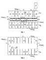
- FIGS. 1 and 2depict opposing sides 8 and 9 , respectively, of a preferred flex circuit 12 (“flex”, “flex circuitry”, “flexible circuit”) used in constructing a module according to an embodiment of the present invention.
- Flex circuit 12is preferably made from one or more conductive layers supported by one or more flexible substrate layers as further described with reference to later Figs. The construction of flex circuitry is known in the art.
- the entirety of the flex circuit 12may be flexible or, as those of skill in the art will recognize, the flexible circuit structure 12 may be made flexible in certain areas to allow conformability to required shapes or bends, and rigid in other areas to provide rigid and planar mounting surfaces.
- Preferred flex circuit 12has openings 17 for use in aligning flex circuit 12 to substrate 14 during assembly.
- ICs 18 on flexible circuit 12are, in this embodiment, chip-scale packaged memory devices.
- chip-scale or “CSP”shall refer to integrated circuitry of any function with an array package providing connection to one or more die through contacts (often embodied as “bumps” or “balls” for example) distributed across a major surface of the package or die.
- CSPdoes not refer to leaded devices that provide connection to an integrated circuit within the package through leads emergent from at least one side of the periphery of the package such as, for example, a TSOP.
- Embodiments of the present inventionmay be employed with leaded or CSP devices or other devices in both packaged and unpackaged forms but where the term CSP is used, the above definition for CSP should be adopted. Consequently, although CSP excludes leaded devices, references to CSP are to be broadly construed to include the large variety of array devices (and not to be limited to memory only) and whether die-sized or other size such as BGA and micro BGA as well as flip-chip. As those of skill will understand after appreciating this disclosure, some embodiments of the present invention may be devised to employ stacks of ICs each disposed where an IC 18 is indicated in the exemplar Figs.
- Multiple integrated circuit diemay be included in a package depicted as a single IC 18 . While in this embodiment memory ICs are used to provide a memory expansion board or module, and various embodiments may include a variety of integrated circuits and other components. Such variety may include microprocessors, FPGA's, RF transceiver circuitry, digital logic, as a list of non-limiting examples, or other circuits or systems which may benefit from a high-density circuit board or module capability. Circuit 19 depicted between ICs 18 may be a memory buffer or controller.
- FIG. 1shows two pluralities of ICs 18 along side 8 of flex circuit 12 , the pluralities or sets of ICs being referenced in FIG. 1 as IC R1 and IC R2 .
- Contact arraysare disposed beneath ICs 18 and circuits 19 to provide conductive pads for interconnection to the ICs 18 .
- An exemplar contact array 11 Ais shown as is exemplar IC 18 to be mounted at contact array 11 A as depicted.
- the contact arrays 11 A that correspond to an IC row(e.g., IC R1 ) may be considered a contact array set.
- flex circuit 12has two rows (C R1 and C R2 ) of module contacts 20 .
- FIG. 1When flex circuit 12 is folded as depicted in later FIGS. 3 and 4 , side 8 depicted in FIG. 1 is presented at the outside of module 10 .
- the opposing side 9 of flex circuit 12( FIG. 2 ) is on the inside in the configurations of FIGS. 3 and 4 .
- Other embodimentsmay have other numbers of rows and there may be only one such row.
- FIG. 2depicts another two pluralities of ICs 18 along side 9 of flex circuit 12 referenced as IC R3 and IC R4 .
- Various discrete componentssuch as termination resistors, bypass capacitors, and bias resistors may also be mounted on each of sides 8 and 9 of flex 12 . Such discrete components are not shown to simplify the drawing.
- Flex circuit 12may also depicted with reference to its perimeter edges, two of which are typically long (PE long1 and PE long2 ) and two of which are typically shorter (PE short1 and PE short2 )
- Other embodimentsmay employ flex circuits 12 that are not rectangular in shape and may be square in which case the perimeter edges would be of equal size or other convenient shape to adapt to manufacturing particulars.
- rectangular shapes for flex circuit 12assist in providing a low profile for a preferred module devised with use of flex circuit 12 .
- FIG. 1depicts exemplar conductive traces 21 connecting rows C R1 and C R2 of module contacts 20 to ICs 18 . Only a few exemplar traces are shown to simplify the drawing. Traces 21 may also connect to vias that may transit to other conductive layers of flex 12 in certain embodiments having more than one conductive layer. Shown is a via 23 connecting a signal trace from circuit 19 to a trace 25 disposed on another conductive layer of flex 12 as illustrated by the dotted line of trace 25 . In a preferred embodiment, vias connect ICs 18 on side 9 of flex 12 ( FIG. 2 ) to module contacts 20 .
- Traces 21 and 25may make other connections between the ICs on either side of flex 12 and may traverse the rows of module contacts 20 to interconnect ICs. Together the various traces and vias make interconnections needed to convey data and control signals to the various ICs.
- the present inventionmay be implemented with only a single row of module contacts 20 and may, in other embodiments be implemented as a module bearing ICs on only one side of flex circuit 12 or with fewer or greater numbers of ICs 18 or rows of ICs 18 .
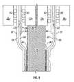
- FIG. 3is a cross section view of a module 10 devised in accordance with a preferred embodiment of the present invention.
- Module 10is populated with ICs 18 having top surfaces 18 T and bottom surfaces 18 B .
- Substrate 14 or support structurehas first and second perimeter edges 16 A and 16 B appearing in the depiction of FIG. 3 as ends.
- Substrate or support structure 14typically has first and second lateral sides S 1 and S 2 .
- Flex 12is wrapped about perimeter edge 16 A of substrate 14 , which in the depicted embodiment, provides the basic shape of a common DIMM board form factor such as that defined by JEDEC standard MO-256.
- Those of skillwill recognize that transitting flex circuit 12 about support structure or substrate 14 as depicted separates a first set of CSPs from a second set of CSPs based upon which lateral side of substrate 14 with which the CSPs are then associated.
- the inner pair of the four depicted ICs 18pass through windows 250 in substrate 14 as shown in later Figs. in further detail and the inner ICs 18 are preferably attached to each other's upper surfaces 18 T with a thermally conductive adhesive 30 . While in this embodiment, the four depicted ICs are attached to flex circuit 12 in opposing pairs, fewer or greater numbers of ICs may be connected in other arrangements such as, for example, staggered or offset arrangements they may exhibit preferred thermal characteristics. Further, while only CSP packaged ICs are shown, other ICs and components may be employed such as leaded devices. In a preferred embodiment, ICs 18 will be memory CSPs and various discrete components such as, for example, resistors and capacitors will also be mounted on flex circuit 12 . To simplify the drawing, the discrete components are not shown.
- flex circuit 12has module contacts 20 positioned in a manner devised to fit in a circuit board card edge connector or socket and connect to corresponding contacts in the connector (not shown). While module contacts 20 are shown protruding from the surface of flex circuit 12 , other embodiments may have flush contacts or contacts below the surface level of flex 12 . Substrate 14 supports module contacts 20 from behind flex circuit 12 in a manner devised to provide the mechanical form required for insertion into a socket. In other embodiments, the thickness or shape of substrate 14 in the vicinity of perimeter edge 16 A may differ from that in the vicinity of perimeter edge 16 B.
- Substrate 14 in the depicted embodimentis preferably made of a metal such as aluminum or copper, as non-limiting examples, or where thermal management is less of an issue, materials such as FR4 (flame retardant type 4) epoxy laminate, PTFE (poly-tetra-fluoro-ethylene) or plastic.
- FR4flame retardant type 4
- PTFEpoly-tetra-fluoro-ethylene
- advantageous features from multiple technologiesmay be combined with use of FR4 having a layer of copper on both sides to provide a substrate 14 devised from familiar materials which may provide heat conduction or a ground plane.
- FIG. 4is an enlarged view of the area marked ‘A’ in FIG. 3 .
- Edge 16 A of substrate 14is shaped like a male side edge of an edge card connector. While a particular oval-like configuration is shown, edge 16 A may take on other shapes devised to mate with various connectors or sockets. The form and function of various edge card connectors are well know in the art.
- flex 12is wrapped around edge 16 A of substrate 14 and may be laminated or adhesively connected to substrate 14 with adhesive 30 . The depicted adhesive 30 and flex 12 may vary in thickness and are not drawn to scale to simplify the drawing.
- the depicted substrate 14has a thickness such that when assembled with the flex 12 and adhesive 30 , the thickness measured between module contacts 20 falls in the range specified for the mating connector.
- flex circuit 12may be wrapped about perimeter edge 16 B or both perimeter edges 16 A and 16 B of substrate 14 .
- multiple flex circuitsmay be employed or a single flex circuit may connect one or both sets of contacts 20 to the resident ICs.
- FIG. 5is an enlarged view of a portion of one preferred embodiment showing lower IC 18 1 and upper IC 18 2 .
- conductive layer 66 of flex circuit 12contains conductive traces connecting module contacts 20 to BGA contacts 63 on ICs 18 1 and 18 2 .
- the number of layersmay be devised in a manner to achieve the bend radius required in those embodiments that bend flex circuit 12 around edge 16 A ( FIG. 4 ) or 16 B, for example.
- the number of layers in any particular portion of flex circuit 12may also be devised to achieve the necessary connection density given a particular minimum trace width associated with the flex circuit technology used.
- Some flex circuits 12may have three or four or more conductive layers.
- Such layersmay be beneficial to route signals for applications such as, for example, a FB-DIMM (fully-buffered DIMM) which may have fewer DIMM input/output signals than a registered DIMM, but may have more interconnect traces required among devices on the DIMM, such as, for example, the C/A copy A and C/A copy B (command/address) signals produced by an FB-DIMM advanced memory buffer (AMB).
- FB-DIMMfully-buffered DIMM
- AMBFB-DIMM advanced memory buffer
- Conductive layers 64 and 66express conductive traces that connect to the ICs and may further connect to other discrete components (not shown).
- the conductive layersare metal such as, for example, copper or alloy 110 .
- Vias such as the exemplar vias 23connect the two conductive layers 64 and 66 and thereby enable connection between conductive layer 64 and module contacts 20 .
- the two conductive layers 64 and 66may be devised in a manner so that one of them has substantial area employed as a ground plane. The other layer may employ substantial area as a voltage reference plane.
- flex circuit 12may in some embodiments be rigid portions (rigid-flex). Construction of rigid-flex circuitry is known in the art.
- Flex circuit 12may be particularly devised to operate as a heat spreader or sink adding to the thermal conduction out of ICs 18 1 and 18 2 .
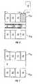
- FIG. 6depicts an exemplar contact-bearing first side of a flex circuit devised in accordance with a preferred embodiment of the present invention.
- the depiction of FIG. 6is simplified to show more clearly the principles of the invention but depicts fewer ICs 18 than would typically be presented on a flex circuit 12 devised for use in embodiments of the present invention.
- An embodiment with more ICs 18is shown in FIG. 1 .
- the principles of the present inventionmay, however, be employed where only one IC 18 is resident on a side of a flex circuit 12 or where multiple rows or sets of ICS are resident on a side of flex circuit 12 .
- FIG. 7depicts the second side of the flex circuit of FIG. 6 .
- FIG. 7in the interests of clarity, illustrates the embodiment with fewer ICs 18 than would typically be employed in an actual embodiment of the invention devised in accord with the principles described herein.
- FIG. 8depicts an exemplar substrate formed to be employed with the exemplar flex circuit depicted in FIG. 7 .
- the second side 9 of flex circuit 12 shown in FIG. 7is folded about substrate 14 shown in FIG. 8 to place ICs 18 into the windows 250 arrayed along substrate 14 .
- ICs along rows ICR 3 and ICR 4being disposed back to back within windows 250 .
- a thermally conductive adhesive or glueis used on the upper sides of ICs 18 to encourage thermal energy flow as well as provide some mechanical advantages.
- FIG. 6depicts the first or, in this case, the outer side of the flex circuit once combined with substrate 14 , the flex circuit itself will have staggered mounting arrays 11 A on side 8 of flex circuit 12 relative to side 9 of flex circuit 12 . This is merely one relative arrangement between ICs 18 on respective sides of substrate 14 .
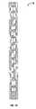
- FIG. 9depicts a view along the line A-A shown in FIG. 8 with flex circuit 12 combined with substrate 14 .
- ICs 18which are on second side 9 (which in this depiction is the inner side with respect to the module 10 ) of populated flex circuit 12 are disposed in windows 250 so that the upper surfaces 18 T of ICs 18 of row ICR 3 are in close proximity with the upper surfaces 18 T of ICs 18 of row ICR 4 .
- these first and second groups of ICsare positioned in the cutaway areas of the first and second lateral sides, respectively, of substrate 14 .
- the cutaway areas on each lateral side of substrate 14are in spatial coincidence to create windows 250 .
- Profile Pis approximately the sum of the distances between the upper and lower surfaces of IC 18 plus 4 ⁇ the diameter of the BGA contacts 63 plus 2 ⁇ the thickness of flex circuit 12 in addition to any adhesive layers 30 employed to adhere one IC 18 to another. This profile dimension will vary depending upon whether BGA contacts 63 are disposed below the surface of flex circuit 12 to reach an appropriate conductive layer or contacts which typically are a part of flex circuit 12 .
- FIG. 10is another depiction of the relationship between flex circuit 12 , and a substrate 14 which has been patterned or windowed with cutaway areas.
- the view of FIG. 10is taken along a line that would intersect the bodies of ICs 18 .
- ICs 18 that comprise row or group ICR 3are staggered relative to those that comprise row or group ICR 4 of second side 9 of flex circuit 12 when module 10 is assembled and flex circuit 12 is combined with substrate 14 . This staggering may result in some construction benefits providing a mechanical “step” for ICs 18 as they are fitted into substrate 14 and may further provide some thermal advantages increasing the contact area between substrate 14 and the plurality of ICs 18 .
- FIG. 11depicts exemplar substrate 14 employed in FIG. 10 before being combined with populated flex circuit 12 as viewed along a line through windows 250 of substrate 14 .
- a number of cutaway areas or pocketsare delineated with dotted lines and identified with references 250 B 3 and 250 B 4 , respectively.
- Those areas identified as 250 B 3correspond, in this example, to the pockets, sites, or cutaway areas on one side of substrate 14 into which ICs 18 from ICR 3 of flex circuit 12 will be disposed when substrate 14 and flex circuit 12 are combined.
- Those pocket, sites, or cutaway areas identified as references 250 B 4correspond to the sites into which ICs 18 from ICR 4 will be disposed. In alternate embodiments, there may be more than one row of ICs 18 disposed on a single side of substrate 14 .
- windowmay refer to an opening all the way through substrate 14 across span “S” which corresponds to the width or height dimension of packaged IC 18 , or it may also refer to that opening where cutaway areas on each of the two sides of substrate 14 overlap.
- FIG. 12depicts the substrate 14 previously depicted in FIG. 11 along the line represented by C. Where cutaway areas 250 B 3 and 250 B 4 overlap, there are, as depicted, windows all the way through substrate 14 . In some embodiments, cutaway areas 250 B 3 and 250 B 4 may not overlap or in other embodiments, there may be pockets or cutaway areas only on one side of substrate 14 . Those of skill will recognize that cutaway areas such as those identified with references 250 B 3 and 250 B 4 may be formed in a variety of ways depending on the material of substrate 14 and need not literally be “cut” away but may be formed by a variety of molding, milling and cutting processes as is understood by those in the field.
- FIG. 13depicts another module having a thinned portion of substrate 14 .
- substrate 14has a first thickness 1 toward edge 16 A devised to provide support for an edge and surrounding area of module assembly 10 as may be needed for connection to a card edge connector.
- a portion 92 having thickness 2Above the portion of substrate 14 with thickness 1 is a portion 92 having thickness 2 .
- FIG. 14depicts another embodiment of the present invention.
- Depicted extension 112 of substrate 14extends beyond the top of flex 12 and is shaped to provide additional surface area for convective cooling. Such shape may be achieved by methods such as, for example, milling or extrusion, which are both known in the art.
- extruded aluminumis used for substrate 14 in this and similar embodiments.
- the embodiment depicted in FIG. 14employs two flex circuits 12 A and 12 B thus presenting an embodiment in which the flex circuit does not wrap about end 16 A of substrate 14 .
- the innermost ICs 18are shown disposed in windows with their respective upper surfaces 18 T connected with an adhesive 30 which is preferably thermally conductive.
- FIG. 15depicts another embodiment of the invention having additional ICs 18 .
- four flex level transitions 26connect to four mounting portions 28 of flex circuits 12 A 1 , 12 A 2 , 12 B 1 , and 12 B 2 .
- Each mounting portion 28has ICs 18 on both sides.
- Flex circuitry 12may also be provided in this configuration by, for example, having a split flex with layers interconnected with vias.
- module 10 of FIG. 15exhibits eight (8) ICs 18 coincident with a single window site 250 in substrate 14 .
- module 10the possibilities for large capacity iterations of module 10 are magnified by such strategies and the same principles may be employed where the ICs 18 on one side of substrate 14 are staggered relative to those ICs 18 on the other side of substrate 14 .
- module 10Four flex circuits are employed in module 10 as depicted in FIG. 15 and, although those embodiments that wrap flex circuit 12 about end 16 A of substrate 14 present manufacturing efficiencies, in some environments having flex circuitry separate from each other on respective sides S 1 and S 2 of substrate 14 may be desirable.
- FIG. 16depicts another embodiment in which flex circuit 12 connects ICs 18 fitted on respective sides into windows 250 and connected face to face with BGA contacts 63 facing each other on opposite sides of flex circuit 12 which is split at juncture 50 into flex circuits 12 S 1 and 12 S 2 that convey signals from ICs 18 to module contacts 20 .
- flex circuit 12is placed flat and both sides populated according to circuit board assembly techniques known in the art. Flex circuit 12 is then folded about end 16 A of substrate 14 as ICs 18 are fitted into respective cutout areas of substrate 14 . Tooling holes 17 may be used to align flex 12 to substrate 14 . Flex 12 may be laminated or otherwise attached to substrate 14 .
Landscapes
- Engineering & Computer Science (AREA)
- Power Engineering (AREA)
- Microelectronics & Electronic Packaging (AREA)
- Physics & Mathematics (AREA)
- Condensed Matter Physics & Semiconductors (AREA)
- General Physics & Mathematics (AREA)
- Computer Hardware Design (AREA)
- Structure Of Printed Boards (AREA)
- Combinations Of Printed Boards (AREA)
Abstract
Description
Claims (7)
Priority Applications (25)
| Application Number | Priority Date | Filing Date | Title |
|---|---|---|---|
| US11/005,992US7480152B2 (en) | 2004-09-03 | 2004-12-07 | Thin module system and method |
| US11/058,979US7468893B2 (en) | 2004-09-03 | 2005-02-16 | Thin module system and method |
| US11/077,952US7606040B2 (en) | 2004-09-03 | 2005-03-11 | Memory module system and method |
| US11/123,721US20060053345A1 (en) | 2004-09-03 | 2005-05-06 | Thin module system and method |
| US11/125,018US7606049B2 (en) | 2004-09-03 | 2005-05-09 | Module thermal management system and method |
| PCT/US2005/028547WO2006028643A2 (en) | 2004-09-03 | 2005-08-10 | Circuit module system and method |
| CA002515714ACA2515714A1 (en) | 2004-09-03 | 2005-08-11 | Circuit module system and method |
| AU2005203591AAU2005203591A1 (en) | 2004-09-03 | 2005-08-11 | Circuit module system and method |
| FR0508522AFR2878118A1 (en) | 2004-09-03 | 2005-08-11 | CIRCUIT MODULE, METHOD FOR ASSEMBLING THE SAME, SYSTEM FOR EXTRACTING HEAT ENERGY FROM CIRCUIT MODULE, AND THERMAL MANAGEMENT SYSTEM |
| GB0516622AGB2417836B (en) | 2004-09-03 | 2005-08-12 | Circuit module system and method |
| GB0822085AGB2452880B (en) | 2004-09-03 | 2005-08-12 | Circuit module system and method |
| DE102005038254ADE102005038254A1 (en) | 2004-09-03 | 2005-08-12 | Circuit module system and method |
| GB0822086AGB2453064A (en) | 2004-09-03 | 2005-08-12 | Circuit module for memory expansion |
| JP2005235451AJP2006074031A (en) | 2004-09-03 | 2005-08-15 | Circuit module system and method |
| KR1020050074824AKR100880054B1 (en) | 2004-09-03 | 2005-08-16 | Circuit module system and method |
| US11/231,418US7443023B2 (en) | 2004-09-03 | 2005-09-21 | High capacity thin module system |
| US11/242,962US20060048385A1 (en) | 2004-09-03 | 2005-10-04 | Minimized profile circuit module systems and methods |
| US11/255,061US7542297B2 (en) | 2004-09-03 | 2005-10-19 | Optimized mounting area circuit module system and method |
| US11/283,355US7446410B2 (en) | 2004-09-03 | 2005-11-18 | Circuit module with thermal casing systems |
| US11/331,969US7616452B2 (en) | 2004-09-03 | 2006-01-13 | Flex circuit constructions for high capacity circuit module systems and methods |
| US11/332,740US7579687B2 (en) | 2004-09-03 | 2006-01-13 | Circuit module turbulence enhancement systems and methods |
| US11/397,597US7760513B2 (en) | 2004-09-03 | 2006-04-03 | Modified core for circuit module system and method |
| US11/961,477US7459784B2 (en) | 2004-09-03 | 2007-12-20 | High capacity thin module system |
| US12/258,189US7626259B2 (en) | 2004-09-03 | 2008-10-24 | Heat sink for a high capacity thin module system |
| US12/263,060US7737549B2 (en) | 2004-09-03 | 2008-10-31 | Circuit module with thermal casing systems |
Applications Claiming Priority (2)
| Application Number | Priority Date | Filing Date | Title |
|---|---|---|---|
| US10/934,027US20060050492A1 (en) | 2004-09-03 | 2004-09-03 | Thin module system and method |
| US11/005,992US7480152B2 (en) | 2004-09-03 | 2004-12-07 | Thin module system and method |
Related Parent Applications (7)
| Application Number | Title | Priority Date | Filing Date |
|---|---|---|---|
| US10/934,027Continuation-In-PartUS20060050492A1 (en) | 2004-09-03 | 2004-09-03 | Thin module system and method |
| US11/007,551Continuation-In-PartUS7511968B2 (en) | 2004-09-03 | 2004-12-08 | Buffered thin module system and method |
| US11/231,418Continuation-In-PartUS7443023B2 (en) | 2004-09-03 | 2005-09-21 | High capacity thin module system |
| US11/255,061Continuation-In-PartUS7542297B2 (en) | 2004-09-03 | 2005-10-19 | Optimized mounting area circuit module system and method |
| US11/283,355Continuation-In-PartUS7446410B2 (en) | 2004-09-03 | 2005-11-18 | Circuit module with thermal casing systems |
| US11/331,969Continuation-In-PartUS7616452B2 (en) | 2004-09-03 | 2006-01-13 | Flex circuit constructions for high capacity circuit module systems and methods |
| US11/397,597Continuation-In-PartUS7760513B2 (en) | 2004-09-03 | 2006-04-03 | Modified core for circuit module system and method |
Related Child Applications (13)
| Application Number | Title | Priority Date | Filing Date |
|---|---|---|---|
| US10/934,027Continuation-In-PartUS20060050492A1 (en) | 2004-09-03 | 2004-09-03 | Thin module system and method |
| US11/007,551Continuation-In-PartUS7511968B2 (en) | 2004-09-03 | 2004-12-08 | Buffered thin module system and method |
| US11/058,979Continuation-In-PartUS7468893B2 (en) | 2004-09-03 | 2005-02-16 | Thin module system and method |
| US11/068,688Continuation-In-PartUS7324352B2 (en) | 2004-09-03 | 2005-03-01 | High capacity thin module system and method |
| US11/077,952Continuation-In-PartUS7606040B2 (en) | 2004-09-03 | 2005-03-11 | Memory module system and method |
| US11/123,721Continuation-In-PartUS20060053345A1 (en) | 2004-09-03 | 2005-05-06 | Thin module system and method |
| US11/125,018Continuation-In-PartUS7606049B2 (en) | 2004-09-03 | 2005-05-09 | Module thermal management system and method |
| US11/231,418Continuation-In-PartUS7443023B2 (en) | 2004-09-03 | 2005-09-21 | High capacity thin module system |
| US11/242,962Continuation-In-PartUS20060048385A1 (en) | 2004-09-03 | 2005-10-04 | Minimized profile circuit module systems and methods |
| US11/255,061Continuation-In-PartUS7542297B2 (en) | 2004-09-03 | 2005-10-19 | Optimized mounting area circuit module system and method |
| US11/283,355Continuation-In-PartUS7446410B2 (en) | 2004-09-03 | 2005-11-18 | Circuit module with thermal casing systems |
| US11/331,969Continuation-In-PartUS7616452B2 (en) | 2004-09-03 | 2006-01-13 | Flex circuit constructions for high capacity circuit module systems and methods |
| US11/397,597Continuation-In-PartUS7760513B2 (en) | 2004-09-03 | 2006-04-03 | Modified core for circuit module system and method |
Publications (2)
| Publication Number | Publication Date |
|---|---|
| US20060050496A1 US20060050496A1 (en) | 2006-03-09 |
| US7480152B2true US7480152B2 (en) | 2009-01-20 |
Family
ID=35995989
Family Applications (3)
| Application Number | Title | Priority Date | Filing Date |
|---|---|---|---|
| US10/934,027AbandonedUS20060050492A1 (en) | 2004-09-03 | 2004-09-03 | Thin module system and method |
| US11/005,992Expired - LifetimeUS7480152B2 (en) | 2004-09-03 | 2004-12-07 | Thin module system and method |
| US11/624,608Expired - LifetimeUS7602613B2 (en) | 2004-09-03 | 2007-01-18 | Thin module system and method |
Family Applications Before (1)
| Application Number | Title | Priority Date | Filing Date |
|---|---|---|---|
| US10/934,027AbandonedUS20060050492A1 (en) | 2004-09-03 | 2004-09-03 | Thin module system and method |
Family Applications After (1)
| Application Number | Title | Priority Date | Filing Date |
|---|---|---|---|
| US11/624,608Expired - LifetimeUS7602613B2 (en) | 2004-09-03 | 2007-01-18 | Thin module system and method |
Country Status (2)
| Country | Link |
|---|---|
| US (3) | US20060050492A1 (en) |
| CN (1) | CN1819185A (en) |
Cited By (9)
| Publication number | Priority date | Publication date | Assignee | Title |
|---|---|---|---|---|
| US20060125067A1 (en)* | 2004-09-03 | 2006-06-15 | Staktek Group L.P. | Flex circuit constructions for high capacity circuit module systems and methods |
| US20070126125A1 (en)* | 2005-05-18 | 2007-06-07 | Staktek Group L.P. | Memory Module System and Method |
| US20070194425A1 (en)* | 2006-02-22 | 2007-08-23 | Zingher Arthur R | Single-chip and multi-chip module for proximity communication |
| US20070211711A1 (en)* | 2006-03-08 | 2007-09-13 | Clayton James E | Thin multichip flex-module |
| US20090046431A1 (en)* | 2004-09-03 | 2009-02-19 | Staktek Group L.P. | High Capacity Thin Module System |
| US20110031628A1 (en)* | 2009-08-06 | 2011-02-10 | Fujitsu Limited | Semiconductor device module and method of manufacturing semiconductor device module |
| US20110051385A1 (en)* | 2009-08-31 | 2011-03-03 | Gainteam Holdings Limited | High-density memory assembly |
| US8588017B2 (en) | 2010-10-20 | 2013-11-19 | Samsung Electronics Co., Ltd. | Memory circuits, systems, and modules for performing DRAM refresh operations and methods of operating the same |
| US10417162B2 (en) | 2015-12-04 | 2019-09-17 | Samsung Electronics Co., Ltd. | Memory package including buffer, expansion memory module, and multi-module memory system |
Families Citing this family (83)
| Publication number | Priority date | Publication date | Assignee | Title |
|---|---|---|---|---|
| US7254036B2 (en)* | 2004-04-09 | 2007-08-07 | Netlist, Inc. | High density memory module using stacked printed circuit boards |
| US7542297B2 (en) | 2004-09-03 | 2009-06-02 | Entorian Technologies, Lp | Optimized mounting area circuit module system and method |
| US7606049B2 (en)* | 2004-09-03 | 2009-10-20 | Entorian Technologies, Lp | Module thermal management system and method |
| US7579687B2 (en)* | 2004-09-03 | 2009-08-25 | Entorian Technologies, Lp | Circuit module turbulence enhancement systems and methods |
| US7522421B2 (en) | 2004-09-03 | 2009-04-21 | Entorian Technologies, Lp | Split core circuit module |
| US7606040B2 (en)* | 2004-09-03 | 2009-10-20 | Entorian Technologies, Lp | Memory module system and method |
| US7606050B2 (en)* | 2004-09-03 | 2009-10-20 | Entorian Technologies, Lp | Compact module system and method |
| US7511968B2 (en)* | 2004-09-03 | 2009-03-31 | Entorian Technologies, Lp | Buffered thin module system and method |
| US7446410B2 (en)* | 2004-09-03 | 2008-11-04 | Entorian Technologies, Lp | Circuit module with thermal casing systems |
| US7423885B2 (en)* | 2004-09-03 | 2008-09-09 | Entorian Technologies, Lp | Die module system |
| US7289327B2 (en)* | 2006-02-27 | 2007-10-30 | Stakick Group L.P. | Active cooling methods and apparatus for modules |
| US7468893B2 (en)* | 2004-09-03 | 2008-12-23 | Entorian Technologies, Lp | Thin module system and method |
| US20060053345A1 (en)* | 2004-09-03 | 2006-03-09 | Staktek Group L.P. | Thin module system and method |
| US20060050492A1 (en) | 2004-09-03 | 2006-03-09 | Staktek Group, L.P. | Thin module system and method |
| US7324352B2 (en)* | 2004-09-03 | 2008-01-29 | Staktek Group L.P. | High capacity thin module system and method |
| US7760513B2 (en)* | 2004-09-03 | 2010-07-20 | Entorian Technologies Lp | Modified core for circuit module system and method |
| US20060049513A1 (en)* | 2004-09-03 | 2006-03-09 | Staktek Group L.P. | Thin module system and method with thermal management |
| US20100020515A1 (en)* | 2005-03-08 | 2010-01-28 | Smart Modular Technologies, Inc. | Method and system for manufacturing micro solid state drive devices |
| US7556405B2 (en)* | 2005-07-28 | 2009-07-07 | Velcro Industries B.V. | Mounting light emitting diodes |
| US7442050B1 (en) | 2005-08-29 | 2008-10-28 | Netlist, Inc. | Circuit card with flexible connection for memory module with heat spreader |
| US20080225476A1 (en)* | 2006-01-11 | 2008-09-18 | Chris Karabatsos | Tab wrap foldable electronic assembly module and method of manufacture |
| US8411450B2 (en)* | 2006-01-25 | 2013-04-02 | Nec Corporation | Electronic device package, module, and electronic device |
| US7511969B2 (en)* | 2006-02-02 | 2009-03-31 | Entorian Technologies, Lp | Composite core circuit module system and method |
| US7619893B1 (en) | 2006-02-17 | 2009-11-17 | Netlist, Inc. | Heat spreader for electronic modules |
| US7787254B2 (en)* | 2006-03-08 | 2010-08-31 | Microelectronics Assembly Technologies, Inc. | Thin multichip flex-module |
| US7429788B2 (en)* | 2006-03-08 | 2008-09-30 | Microelectronics Assembly Technologies, Inc. | Thin multichip flex-module |
| US7520781B2 (en)* | 2006-03-08 | 2009-04-21 | Microelectronics Assembly Technologies | Thin multichip flex-module |
| US7393226B2 (en)* | 2006-03-08 | 2008-07-01 | Microelectronics Assembly Technologies, Inc. | Thin multichip flex-module |
| US7394149B2 (en)* | 2006-03-08 | 2008-07-01 | Microelectronics Assembly Technologies, Inc. | Thin multichip flex-module |
| US20070247820A1 (en)* | 2006-04-24 | 2007-10-25 | Foxconn Technology Co., Ltd. | Memory module assembly including heat dissipating members |
| US20070247819A1 (en)* | 2006-04-24 | 2007-10-25 | Foxconn Technology Co., Ltd. | Memory module assembly including heat dissipating members |
| US7252520B1 (en) | 2006-04-25 | 2007-08-07 | Tyco Electronics Corporation | Flex film card edge connector and cable assembly |
| US20080002447A1 (en)* | 2006-06-29 | 2008-01-03 | Smart Modular Technologies, Inc. | Memory supermodule utilizing point to point serial data links |
| US7715200B2 (en) | 2007-09-28 | 2010-05-11 | Samsung Electronics Co., Ltd. | Stacked semiconductor module, method of fabricating the same, and electronic system using the same |
| US20090166065A1 (en)* | 2008-01-02 | 2009-07-02 | Clayton James E | Thin multi-chip flex module |
| JP2009176815A (en)* | 2008-01-22 | 2009-08-06 | Olympus Corp | Mounting structure |
| US8061886B1 (en) | 2008-04-30 | 2011-11-22 | Velcro Industries B.V. | Securing electrical devices |
| US8018723B1 (en) | 2008-04-30 | 2011-09-13 | Netlist, Inc. | Heat dissipation for electronic modules |
| US20100134982A1 (en)* | 2008-12-01 | 2010-06-03 | Meyer Iv George Anthony | Memory heat dissipating structure and memory device having the same |
| US20100134995A1 (en)* | 2008-12-02 | 2010-06-03 | Raytheon Company | Electrical Interconnection System |
| US8465327B2 (en)* | 2009-11-02 | 2013-06-18 | Apple Inc. | High-speed memory connector |
| US9320130B2 (en)* | 2010-10-25 | 2016-04-19 | Korea Electric Terminal Co., Ltd. | Printed circuit board, and board block for vehicles using the same |
| US9159647B2 (en)* | 2012-01-27 | 2015-10-13 | Novachips Canada Inc. | Method and apparatus for connecting memory dies to form a memory system |
| USD706203S1 (en) | 2012-03-20 | 2014-06-03 | Wald Llc | Bracket |
| USD722003S1 (en) | 2012-03-20 | 2015-02-03 | Wald Llc | Swivel bracket |
| US8902606B2 (en) | 2012-10-17 | 2014-12-02 | Microelectronics Assembly Technologies | Electronic interconnect system |
| US9338895B2 (en) | 2012-10-17 | 2016-05-10 | Microelectronics Assembly Technologies | Method for making an electrical circuit |
| US8837141B2 (en) | 2012-10-17 | 2014-09-16 | Microelectronics Assembly Technologies | Electronic module with heat spreading enclosure |
| US8899994B2 (en) | 2012-10-17 | 2014-12-02 | Microelectronics Assembly Technologies, Inc. | Compression connector system |
| US8817458B2 (en) | 2012-10-17 | 2014-08-26 | Microelectronics Assembly Technologies, Inc. | Flexible circuit board and connection system |
| US8834182B2 (en) | 2012-10-17 | 2014-09-16 | Microelectronics Assembly Technologies | Pierced flexible circuit and compression joint |
| US8559183B1 (en)* | 2013-01-02 | 2013-10-15 | iJet Technologies, Inc. | Method to use empty slots in onboard aircraft servers and communication devices to install non-proprietary servers and communications interfaces |
| US9648754B1 (en) | 2013-11-12 | 2017-05-09 | Smart Modular Technologies, Inc. | Integrated circuit device system with elevated stacked configuration and method of manufacture thereof |
| US9384104B2 (en) | 2013-11-27 | 2016-07-05 | International Business Machines Corporation | Testing a processor assembly |
| US9496633B1 (en) | 2015-06-22 | 2016-11-15 | Intel Corporation | Memory module adaptor card |
| DE102016115665B3 (en) | 2016-08-24 | 2018-01-18 | Harting Electric Gmbh & Co. Kg | Connectors |
| US10679722B2 (en) | 2016-08-26 | 2020-06-09 | Sandisk Technologies Llc | Storage system with several integrated components and method for use therewith |
| US10321587B2 (en) | 2017-02-03 | 2019-06-11 | Google Llc | Integrated connector receptacle device |
| US9900999B1 (en) | 2017-02-03 | 2018-02-20 | Google Inc. | Circuit board architecture for an electronic device |
| US10209796B2 (en) | 2017-02-03 | 2019-02-19 | Google Llc | Display assembly connector device |
| TWD189071S (en)* | 2017-02-17 | 2018-03-11 | 三星電子股份有限公司 | Ssd storage device |
| TWD189069S (en)* | 2017-02-17 | 2018-03-11 | 三星電子股份有限公司 | Ssd storage device |
| TWD189067S (en)* | 2017-02-17 | 2018-03-11 | 三星電子股份有限公司 | Ssd storage device |
| TWD189070S (en)* | 2017-02-17 | 2018-03-11 | 三星電子股份有限公司 | Ssd storage device |
| TWD189065S (en)* | 2017-02-17 | 2018-03-11 | 三星電子股份有限公司 | Ssd storage device |
| TWD190983S (en)* | 2017-02-17 | 2018-06-11 | 三星電子股份有限公司 | Ssd storage device |
| TWD189068S (en)* | 2017-02-17 | 2018-03-11 | 三星電子股份有限公司 | Ssd storage device |
| TWD189066S (en)* | 2017-02-17 | 2018-03-11 | 三星電子股份有限公司 | Ssd storage device |
| US10721825B2 (en) | 2017-08-18 | 2020-07-21 | Google Llc | Bent display panel with electrical lines for a sensor |
| US10299405B2 (en)* | 2017-10-02 | 2019-05-21 | Plume Design, Inc. | Mid-spreader for stacked circuit boards in an electronic device |
| US10342132B2 (en)* | 2017-12-12 | 2019-07-02 | Intel Corporation | Memory device with insertable portion |
| CN109935248B (en)* | 2017-12-18 | 2021-04-13 | 陈松佑 | memory module card |
| CN108012224B (en)* | 2017-12-29 | 2023-11-21 | 歌尔股份有限公司 | Vibrating diaphragm and electroacoustic transducer |
| USD869469S1 (en)* | 2018-04-09 | 2019-12-10 | Samsung Electronics Co., Ltd. | SSD storage device |
| USD869470S1 (en)* | 2018-04-09 | 2019-12-10 | Samsung Electronics Co., Ltd. | SSD storage device |
| CN109688701B (en)* | 2018-06-26 | 2021-08-03 | 上海嘉捷通电路科技股份有限公司 | A rigid-flex PCB board |
| USD897345S1 (en)* | 2018-12-07 | 2020-09-29 | Sung-Yu Chen | Double-data-rate SDRAM card |
| USD954061S1 (en)* | 2018-12-07 | 2022-06-07 | Sung-Yu Chen | Double-data-rate SDRAM card |
| US10888010B2 (en)* | 2019-05-24 | 2021-01-05 | Intel Corporation | Retention of dual in-line memory modules |
| CN111511111A (en)* | 2020-06-02 | 2020-08-07 | 武汉世纪中显科技有限公司 | A circuit board assembly of a serial screen |
| KR20220059142A (en)* | 2020-11-02 | 2022-05-10 | 삼성전자주식회사 | Module board and memory module having the same |
| CN113568483B (en)* | 2021-07-26 | 2023-07-14 | 南昌华勤电子科技有限公司 | A cooling component and a server |
| CN115119368B (en)* | 2022-07-01 | 2023-09-12 | 扬州灿阳电子科技有限公司 | Street lamp single lamp controller with 4G real-time communication function |
Citations (299)
| Publication number | Priority date | Publication date | Assignee | Title |
|---|---|---|---|---|
| US3372310A (en) | 1965-04-30 | 1968-03-05 | Radiation Inc | Universal modular packages for integrated circuits |
| US3436604A (en) | 1966-04-25 | 1969-04-01 | Texas Instruments Inc | Complex integrated circuit array and method for fabricating same |
| US3582865A (en) | 1969-12-16 | 1971-06-01 | Ibm | Microcircuit module and connector |
| US3654394A (en) | 1969-07-08 | 1972-04-04 | Gordon Eng Co | Field effect transistor switch, particularly for multiplexing |
| US3704455A (en) | 1971-02-01 | 1972-11-28 | Alfred D Scarbrough | 3d-coaxial memory construction and method of making |
| US3718842A (en) | 1972-04-21 | 1973-02-27 | Texas Instruments Inc | Liquid crystal display mounting structure |
| US3727064A (en) | 1971-03-17 | 1973-04-10 | Monsanto Co | Opto-isolator devices and method for the fabrication thereof |
| US3746934A (en) | 1971-05-06 | 1973-07-17 | Siemens Ag | Stack arrangement of semiconductor chips |
| US3766439A (en) | 1972-01-12 | 1973-10-16 | Gen Electric | Electronic module using flexible printed circuit board with heat sink means |
| US3772776A (en) | 1969-12-03 | 1973-11-20 | Thomas & Betts Corp | Method of interconnecting memory plane boards |
| JPS5385159U (en) | 1976-12-15 | 1978-07-13 | ||
| US4169642A (en) | 1976-09-16 | 1979-10-02 | E. I. Du Pont De Nemours And Company | Integrated circuit connector |
| US4288841A (en) | 1979-09-20 | 1981-09-08 | Bell Telephone Laboratories, Incorporated | Double cavity semiconductor chip carrier |
| US4342069A (en) | 1979-07-02 | 1982-07-27 | Mostek Corporation | Integrated circuit package |
| US4429349A (en) | 1980-09-30 | 1984-01-31 | Burroughs Corporation | Coil connector |
| US4437235A (en) | 1980-12-29 | 1984-03-20 | Honeywell Information Systems Inc. | Integrated circuit package |
| GB2130025A (en) | 1982-11-08 | 1984-05-23 | Control Data Corp | Memory board stacking module |
| US4513368A (en) | 1981-05-22 | 1985-04-23 | Data General Corporation | Digital data processing system having object-based logical memory addressing and self-structuring modular memory |
| US4547834A (en) | 1982-12-30 | 1985-10-15 | Thomson-Csf | Structure for assembling complex electronic circuits |
| US4567543A (en) | 1983-02-15 | 1986-01-28 | Motorola, Inc. | Double-sided flexible electronic circuit module |
| US4587596A (en) | 1984-04-09 | 1986-05-06 | Amp Incorporated | High density mother/daughter circuit board connector |
| US4645944A (en) | 1983-09-05 | 1987-02-24 | Matsushita Electric Industrial Co., Ltd. | MOS register for selecting among various data inputs |
| US4656605A (en) | 1983-09-02 | 1987-04-07 | Wang Laboratories, Inc. | Single in-line memory module |
| US4672421A (en) | 1984-04-02 | 1987-06-09 | Motorola, Inc. | Semiconductor packaging and method |
| US4682207A (en) | 1982-03-17 | 1987-07-21 | Fujitsu Limited | Semiconductor device including leadless packages and a base plate for mounting the leadless packages |
| US4696525A (en) | 1985-12-13 | 1987-09-29 | Amp Incorporated | Socket for stacking integrated circuit packages |
| US4709300A (en) | 1986-05-05 | 1987-11-24 | Itt Gallium Arsenide Technology Center, A Division Of Itt Corporation | Jumper for a semiconductor assembly |
| US4724611A (en) | 1985-08-23 | 1988-02-16 | Nec Corporation | Method for producing semiconductor module |
| US4727513A (en) | 1983-09-02 | 1988-02-23 | Wang Laboratories, Inc. | Signal in-line memory module |
| US4733461A (en) | 1984-12-28 | 1988-03-29 | Micro Co., Ltd. | Method of stacking printed circuit boards |
| US4739589A (en) | 1985-07-12 | 1988-04-26 | Wacker-Chemitronic Gesellschaft Fur Elektronik-Grundstoff Mbh | Process and apparatus for abrasive machining of a wafer-like workpiece |
| US4763188A (en) | 1986-08-08 | 1988-08-09 | Thomas Johnson | Packaging system for multiple semiconductor devices |
| US4771366A (en) | 1987-07-06 | 1988-09-13 | International Business Machines Corporation | Ceramic card assembly having enhanced power distribution and cooling |
| US4821007A (en) | 1987-02-06 | 1989-04-11 | Tektronix, Inc. | Strip line circuit component and method of manufacture |
| US4823234A (en) | 1985-08-16 | 1989-04-18 | Dai-Ichi Seiko Co., Ltd. | Semiconductor device and its manufacture |
| US4833568A (en) | 1988-01-29 | 1989-05-23 | Berhold G Mark | Three-dimensional circuit component assembly and method corresponding thereto |
| US4850892A (en) | 1985-12-16 | 1989-07-25 | Wang Laboratories, Inc. | Connecting apparatus for electrically connecting memory modules to a printed circuit board |
| US4862249A (en) | 1987-04-17 | 1989-08-29 | Xoc Devices, Inc. | Packaging system for stacking integrated circuits |
| US4911643A (en) | 1988-10-11 | 1990-03-27 | Beta Phase, Inc. | High density and high signal integrity connector |
| US4953060A (en) | 1989-05-05 | 1990-08-28 | Ncr Corporation | Stackable integrated circuit chip package with improved heat removal |
| US4956694A (en) | 1988-11-04 | 1990-09-11 | Dense-Pac Microsystems, Inc. | Integrated circuit chip stacking |
| US4972580A (en) | 1988-06-24 | 1990-11-27 | Kabushiki Kaisha Toshiba | Method for connecting electronic components with dummy patterns |
| US4982265A (en) | 1987-06-24 | 1991-01-01 | Hitachi, Ltd. | Semiconductor integrated circuit device and method of manufacturing the same |
| US4983533A (en) | 1987-10-28 | 1991-01-08 | Irvine Sensors Corporation | High-density electronic modules - process and product |
| US4985703A (en) | 1988-02-03 | 1991-01-15 | Nec Corporation | Analog multiplexer |
| US4992850A (en) | 1989-02-15 | 1991-02-12 | Micron Technology, Inc. | Directly bonded simm module |
| US4992849A (en) | 1989-02-15 | 1991-02-12 | Micron Technology, Inc. | Directly bonded board multiple integrated circuit module |
| JPH03102862A (en) | 1989-09-18 | 1991-04-30 | Fujitsu Ltd | Semiconductor device |
| US5014161A (en) | 1985-07-22 | 1991-05-07 | Digital Equipment Corporation | System for detachably mounting semiconductors on conductor substrate |
| US5014115A (en) | 1987-11-16 | 1991-05-07 | Motorola, Inc. | Coplanar waveguide semiconductor package |
| US5016138A (en) | 1987-10-27 | 1991-05-14 | Woodman John K | Three dimensional integrated circuit package |
| US5025306A (en) | 1988-08-09 | 1991-06-18 | Texas Instruments Incorporated | Assembly of semiconductor chips |
| US5034350A (en) | 1987-09-23 | 1991-07-23 | Sgs Thomson Microelectronics S.R.L. | Semiconductor device package with dies mounted on both sides of the central pad of a metal frame |
| US5041015A (en) | 1990-03-30 | 1991-08-20 | Cal Flex, Inc. | Electrical jumper assembly |
| US5053853A (en) | 1990-05-08 | 1991-10-01 | International Business Machines Corporation | Modular electronic packaging system |
| US5065277A (en) | 1990-07-13 | 1991-11-12 | Sun Microsystems, Inc. | Three dimensional packaging arrangement for computer systems and the like |
| US5099393A (en) | 1991-03-25 | 1992-03-24 | International Business Machines Corporation | Electronic package for high density applications |
| US5104820A (en) | 1989-07-07 | 1992-04-14 | Irvine Sensors Corporation | Method of fabricating electronic circuitry unit containing stacked IC layers having lead rerouting |
| US5109318A (en) | 1990-05-07 | 1992-04-28 | International Business Machines Corporation | Pluggable electronic circuit package assembly with snap together heat sink housing |
| US5117282A (en) | 1990-10-29 | 1992-05-26 | Harris Corporation | Stacked configuration for integrated circuit devices |
| US5119269A (en) | 1989-08-23 | 1992-06-02 | Seiko Epson Corporation | Semiconductor with a battery unit |
| US5138434A (en) | 1991-01-22 | 1992-08-11 | Micron Technology, Inc. | Packaging for semiconductor logic devices |
| US5138430A (en) | 1991-06-06 | 1992-08-11 | International Business Machines Corporation | High performance versatile thermally enhanced IC chip mounting |
| US5140405A (en) | 1990-08-30 | 1992-08-18 | Micron Technology, Inc. | Semiconductor assembly utilizing elastomeric single axis conductive interconnect |
| US5159535A (en) | 1987-03-11 | 1992-10-27 | International Business Machines Corporation | Method and apparatus for mounting a flexible film semiconductor chip carrier on a circuitized substrate |
| US5173840A (en) | 1990-05-07 | 1992-12-22 | Mitsubishi Denki Kabushiki Kaisha | Molded ic card |
| US5191404A (en) | 1989-12-20 | 1993-03-02 | Digital Equipment Corporation | High density memory array packaging |
| US5208729A (en) | 1992-02-14 | 1993-05-04 | International Business Machines Corporation | Multi-chip module |
| US5214845A (en) | 1992-05-11 | 1993-06-01 | Micron Technology, Inc. | Method for producing high speed integrated circuits |
| US5219377A (en) | 1992-01-17 | 1993-06-15 | Texas Instruments Incorporated | High temperature co-fired ceramic integrated phased array package |
| US5222014A (en) | 1992-03-02 | 1993-06-22 | Motorola, Inc. | Three-dimensional multi-chip pad array carrier |
| US5224023A (en) | 1992-02-10 | 1993-06-29 | Smith Gary W | Foldable electronic assembly module |
| US5229917A (en) | 1992-07-24 | 1993-07-20 | The United States Of America As Represented By The Secretary Of The Air Force | VLSI integration into a 3-D WSI dual composite module |
| US5229916A (en) | 1992-03-04 | 1993-07-20 | International Business Machines Corporation | Chip edge interconnect overlay element |
| US5239198A (en) | 1989-09-06 | 1993-08-24 | Motorola, Inc. | Overmolded semiconductor device having solder ball and edge lead connective structure |
| US5241454A (en) | 1992-01-22 | 1993-08-31 | International Business Machines Corporation | Mutlilayered flexible circuit package |
| US5241456A (en) | 1990-07-02 | 1993-08-31 | General Electric Company | Compact high density interconnect structure |
| US5247423A (en) | 1992-05-26 | 1993-09-21 | Motorola, Inc. | Stacking three dimensional leadless multi-chip module and method for making the same |
| US5252857A (en) | 1991-08-05 | 1993-10-12 | International Business Machines Corporation | Stacked DCA memory chips |
| US5261068A (en) | 1990-05-25 | 1993-11-09 | Dell Usa L.P. | Dual path memory retrieval system for an interleaved dynamic RAM memory unit |
| US5259770A (en) | 1992-03-19 | 1993-11-09 | Amp Incorporated | Impedance controlled elastomeric connector |
| US5268815A (en) | 1992-02-14 | 1993-12-07 | International Business Machines Corporation | High density, high performance memory circuit package |
| US5276418A (en) | 1988-11-16 | 1994-01-04 | Motorola, Inc. | Flexible substrate electronic assembly |
| US5281852A (en) | 1991-12-10 | 1994-01-25 | Normington Peter J C | Semiconductor device including stacked die |
| US5289062A (en) | 1991-03-18 | 1994-02-22 | Quality Semiconductor, Inc. | Fast transmission gate switch |
| US5309986A (en) | 1992-11-30 | 1994-05-10 | Satomi Itoh | Heat pipe |
| US5313097A (en) | 1992-11-16 | 1994-05-17 | International Business Machines, Corp. | High density memory module |
| US5347428A (en) | 1992-12-03 | 1994-09-13 | Irvine Sensors Corporation | Module comprising IC memory stack dedicated to and structurally combined with an IC microprocessor chip |
| US5375041A (en) | 1992-12-02 | 1994-12-20 | Intel Corporation | Ra-tab array bump tab tape based I.C. package |
| US5386341A (en) | 1993-11-01 | 1995-01-31 | Motorola, Inc. | Flexible substrate folded in a U-shape with a rigidizer plate located in the notch of the U-shape |
| US5394300A (en) | 1992-09-04 | 1995-02-28 | Mitsubishi Denki Kabushiki Kaisha | Thin multilayered IC memory card |
| US5397916A (en) | 1991-12-10 | 1995-03-14 | Normington; Peter J. C. | Semiconductor device including stacked die |
| US5400003A (en) | 1992-08-19 | 1995-03-21 | Micron Technology, Inc. | Inherently impedance matched integrated circuit module |
| US5428190A (en) | 1993-07-02 | 1995-06-27 | Sheldahl, Inc. | Rigid-flex board with anisotropic interconnect and method of manufacture |
| US5438224A (en) | 1992-04-23 | 1995-08-01 | Motorola, Inc. | Integrated circuit package having a face-to-face IC chip arrangement |
| US5448511A (en) | 1994-06-01 | 1995-09-05 | Storage Technology Corporation | Memory stack with an integrated interconnect and mounting structure |
| US5477082A (en) | 1994-01-11 | 1995-12-19 | Exponential Technology, Inc. | Bi-planar multi-chip module |
| US5491612A (en) | 1995-02-21 | 1996-02-13 | Fairchild Space And Defense Corporation | Three-dimensional modular assembly of integrated circuits |
| US5502333A (en) | 1994-03-30 | 1996-03-26 | International Business Machines Corporation | Semiconductor stack structures and fabrication/sparing methods utilizing programmable spare circuit |
| US5523695A (en) | 1994-08-26 | 1996-06-04 | Vlsi Technology, Inc. | Universal test socket for exposing the active surface of an integrated circuit in a die-down package |
| US5523619A (en) | 1993-11-03 | 1996-06-04 | International Business Machines Corporation | High density memory structure |
| US5541812A (en) | 1995-05-22 | 1996-07-30 | Burns; Carmen D. | Bus communication system for stacked high density integrated circuit packages having an intermediate lead frame |
| US5572065A (en) | 1992-06-26 | 1996-11-05 | Staktek Corporation | Hermetically sealed ceramic integrated circuit heat dissipating package |
| US5600178A (en) | 1993-10-08 | 1997-02-04 | Texas Instruments Incorporated | Semiconductor package having interdigitated leads |
| US5612570A (en) | 1995-04-13 | 1997-03-18 | Dense-Pac Microsystems, Inc. | Chip stack and method of making same |
| US5631193A (en) | 1992-12-11 | 1997-05-20 | Staktek Corporation | High density lead-on-package fabrication method |
| US5642055A (en) | 1990-02-14 | 1997-06-24 | Particle Interconnect, Inc. | Electrical interconnect using particle enhanced joining of metal surfaces |
| US5644161A (en) | 1993-03-29 | 1997-07-01 | Staktek Corporation | Ultra-high density warp-resistant memory module |
| US5646446A (en) | 1995-12-22 | 1997-07-08 | Fairchild Space And Defense Corporation | Three-dimensional flexible assembly of integrated circuits |
| US5654877A (en) | 1991-08-15 | 1997-08-05 | Staktek Corporation | Lead-on-chip integrated circuit apparatus |
| US5661339A (en) | 1992-09-16 | 1997-08-26 | Clayton; James E. | Thin multichip module |
| US5686730A (en) | 1995-05-15 | 1997-11-11 | Silicon Graphics, Inc. | Dimm pair with data memory and state memory |
| US5708297A (en) | 1992-09-16 | 1998-01-13 | Clayton; James E. | Thin multichip module |
| US5714802A (en) | 1991-06-18 | 1998-02-03 | Micron Technology, Inc. | High-density electronic module |
| US5717556A (en) | 1995-04-26 | 1998-02-10 | Nec Corporation | Printed-wiring board having plural parallel-connected interconnections |
| US5729894A (en) | 1992-07-21 | 1998-03-24 | Lsi Logic Corporation | Method of assembling ball bump grid array semiconductor packages |
| US5739887A (en)* | 1994-10-21 | 1998-04-14 | Hitachi, Ltd. | Liquid crystal display device with reduced frame portion surrounding display area |
| US5744862A (en) | 1996-03-29 | 1998-04-28 | Mitsubishi Denki Kabushiki Kaisha | Reduced thickness semiconductor device with IC packages mounted in openings on substrate |
| US5754409A (en)* | 1996-11-06 | 1998-05-19 | Dynamem, Inc. | Foldable electronic assembly module |
| US5764497A (en) | 1995-11-13 | 1998-06-09 | Minolta Co, Ltd. | Circuit board connection method and connection structure |
| US5789815A (en) | 1996-04-23 | 1998-08-04 | Motorola, Inc. | Three dimensional semiconductor package having flexible appendages |
| US5790447A (en) | 1995-05-15 | 1998-08-04 | Silicon Graphics, Inc. | High-memory capacity DIMM with data and state memory |
| US5802395A (en) | 1996-07-08 | 1998-09-01 | International Business Machines Corporation | High density memory modules with improved data bus performance |
| US5805422A (en) | 1994-09-21 | 1998-09-08 | Nec Corporation | Semiconductor package with flexible board and method of fabricating the same |
| US5835988A (en) | 1996-03-27 | 1998-11-10 | Mitsubishi Denki Kabushiki Kaisha | Packed semiconductor device with wrap around external leads |
| US5869353A (en) | 1997-11-17 | 1999-02-09 | Dense-Pac Microsystems, Inc. | Modular panel stacking process |
| US5899705A (en) | 1997-11-20 | 1999-05-04 | Akram; Salman | Stacked leads-over chip multi-chip module |
| US5917709A (en) | 1997-06-16 | 1999-06-29 | Eastman Kodak Company | Multiple circuit board assembly having an interconnect mechanism that includes a flex connector |
| US5926369A (en) | 1998-01-22 | 1999-07-20 | International Business Machines Corporation | Vertically integrated multi-chip circuit package with heat-sink support |
| US5925934A (en) | 1995-10-28 | 1999-07-20 | Institute Of Microelectronics | Low cost and highly reliable chip-sized package |
| US5949657A (en) | 1997-12-01 | 1999-09-07 | Karabatsos; Chris | Bottom or top jumpered foldable electronic assembly |
| US5953215A (en) | 1997-12-01 | 1999-09-14 | Karabatsos; Chris | Apparatus and method for improving computer memory speed and capacity |
| US5953214A (en) | 1994-03-07 | 1999-09-14 | International Business Machines Corporation | Dual substrate package assembly coupled to a conducting member |
| US5959839A (en) | 1997-01-02 | 1999-09-28 | At&T Corp | Apparatus for heat removal using a flexible backplane |
| US5963427A (en) | 1997-12-11 | 1999-10-05 | Sun Microsystems, Inc. | Multi-chip module with flexible circuit board |
| US5973395A (en) | 1996-04-30 | 1999-10-26 | Yamaichi Electronics Co., Ltd. | IC package having a single wiring sheet with a lead pattern disposed thereon |
| US5995370A (en) | 1997-09-01 | 1999-11-30 | Sharp Kabushiki Kaisha | Heat-sinking arrangement for circuit elements |
| US6002589A (en) | 1997-07-21 | 1999-12-14 | Rambus Inc. | Integrated circuit package for coupling to a printed circuit board |
| US6002167A (en) | 1995-09-22 | 1999-12-14 | Hitachi Cable, Ltd. | Semiconductor device having lead on chip structure |
| US6008538A (en) | 1996-10-08 | 1999-12-28 | Micron Technology, Inc. | Method and apparatus providing redundancy for fabricating highly reliable memory modules |
| US6014316A (en) | 1997-06-13 | 2000-01-11 | Irvine Sensors Corporation | IC stack utilizing BGA contacts |
| US6021048A (en) | 1998-02-17 | 2000-02-01 | Smith; Gary W. | High speed memory module |
| US6028352A (en) | 1997-06-13 | 2000-02-22 | Irvine Sensors Corporation | IC stack utilizing secondary leadframes |
| US6028365A (en) | 1998-03-30 | 2000-02-22 | Micron Technology, Inc. | Integrated circuit package and method of fabrication |
| US6034878A (en) | 1996-12-16 | 2000-03-07 | Hitachi, Ltd. | Source-clock-synchronized memory system and memory unit |
| US6038132A (en) | 1996-12-06 | 2000-03-14 | Mitsubishi Denki Kabushiki Kaisha | Memory module |
| US6040624A (en) | 1997-10-02 | 2000-03-21 | Motorola, Inc. | Semiconductor device package and method |
| US6072233A (en) | 1998-05-04 | 2000-06-06 | Micron Technology, Inc. | Stackable ball grid array package |
| US6078515A (en) | 1998-04-14 | 2000-06-20 | Silicon Graphics, Inc. | Memory system with multiple addressing and control busses |
| US6084294A (en) | 1998-08-26 | 2000-07-04 | Mitsubishi Denki Kabushiki Kaisha | Semiconductor device comprising stacked semiconductor elements |
| US6097087A (en) | 1997-10-31 | 2000-08-01 | Micron Technology, Inc. | Semiconductor package including flex circuit, interconnects and dense array external contacts |
| US6111757A (en) | 1998-01-16 | 2000-08-29 | International Business Machines Corp. | SIMM/DIMM memory module |
| US6121676A (en) | 1996-12-13 | 2000-09-19 | Tessera, Inc. | Stacked microelectronic assembly and method therefor |
| USRE36916E (en) | 1995-03-21 | 2000-10-17 | Simple Technology Incorporated | Apparatus for stacking semiconductor chips |
| US6157541A (en) | 1997-12-30 | 2000-12-05 | Siemens Aktiengesellschaft | Stack arrangement for two semiconductor memory chips and printed board for accepting a plurality of such stack arrangements |
| US6172874B1 (en) | 1998-04-06 | 2001-01-09 | Silicon Graphics, Inc. | System for stacking of integrated circuit packages |
| US6178093B1 (en) | 1996-06-28 | 2001-01-23 | International Business Machines Corporation | Information handling system with circuit assembly having holes filled with filler material |
| US6180881B1 (en)* | 1998-05-05 | 2001-01-30 | Harlan Ruben Isaak | Chip stack and method of making same |
| US6187652B1 (en) | 1998-09-14 | 2001-02-13 | Fujitsu Limited | Method of fabrication of multiple-layer high density substrate |
| US6208546B1 (en) | 1996-11-12 | 2001-03-27 | Niigata Seimitsu Co., Ltd. | Memory module |
| US6208521B1 (en) | 1997-05-19 | 2001-03-27 | Nitto Denko Corporation | Film carrier and laminate type mounting structure using same |
| US6205654B1 (en) | 1992-12-11 | 2001-03-27 | Staktek Group L.P. | Method of manufacturing a surface mount package |
| US6214641B1 (en) | 1996-06-25 | 2001-04-10 | Micron Technology, Inc. | Method of fabricating a multi-chip module |
| US6215687B1 (en) | 1996-02-26 | 2001-04-10 | Hitachi, Ltd. | Semiconductor device and process for manufacturing the same |
| US6222737B1 (en) | 1999-04-23 | 2001-04-24 | Dense-Pac Microsystems, Inc. | Universal package and method of forming the same |
| US6222739B1 (en) | 1998-01-20 | 2001-04-24 | Viking Components | High-density computer module with stacked parallel-plane packaging |
| US6225688B1 (en) | 1997-12-11 | 2001-05-01 | Tessera, Inc. | Stacked microelectronic assembly and method therefor |
| US20010001085A1 (en) | 1999-04-16 | 2001-05-10 | Ali Hassanzadeh | Memory module with offset notches for improved insertion and memory module connector |
| US6233650B1 (en) | 1998-04-01 | 2001-05-15 | Intel Corporation | Using FET switches for large memory arrays |
| US6234820B1 (en) | 1997-07-21 | 2001-05-22 | Rambus Inc. | Method and apparatus for joining printed circuit boards |
| US6262895B1 (en) | 2000-01-13 | 2001-07-17 | John A. Forthun | Stackable chip package with flex carrier |
| US6262476B1 (en) | 1998-07-27 | 2001-07-17 | Siemens Aktiengesellschaft | Composite member composed of at least two integrated circuits and method for the manufacture of a composite member composed of at least two integrated circuits |
| US6265660B1 (en) | 1997-07-09 | 2001-07-24 | Micron Technology, Inc. | Package stack via bottom leaded plastic (BLP) packaging |
| US6266252B1 (en) | 1997-12-01 | 2001-07-24 | Chris Karabatsos | Apparatus and method for terminating a computer memory bus |
| EP1119049A2 (en) | 2000-01-18 | 2001-07-25 | Sony Corporation | Laminate type semiconductor apparatus |
| US20010013423A1 (en) | 1996-10-31 | 2001-08-16 | Hormazdyar M. Dalal | Flip chip attach on flexible circuit carrier using chip with metallic cap on solder |
| US6281577B1 (en) | 1996-06-28 | 2001-08-28 | Pac Tech-Packaging Technologies Gmbh | Chips arranged in plurality of planes and electrically connected to one another |
| US6288907B1 (en) | 1996-05-20 | 2001-09-11 | Staktek Group, L.P. | High density integrated circuit module with complex electrical interconnect rails having electrical interconnect strain relief |
| US20010026009A1 (en) | 2000-03-24 | 2001-10-04 | Kensuke Tsunesa | Semiconductor devicse, a semicinductor module loaded with said semiconductor device and a method of manufacturing said semicoductor device |
| US6300679B1 (en) | 1998-06-01 | 2001-10-09 | Semiconductor Components Industries, Llc | Flexible substrate for packaging a semiconductor component |
| US20010028588A1 (en) | 1996-11-19 | 2001-10-11 | Matsushita Electronics Corporation | Semiconductor memory |
| US20010035572A1 (en) | 1999-05-05 | 2001-11-01 | Isaak Harlan R. | Stackable flex circuit chip package and method of making same |
| US6316825B1 (en) | 1998-05-15 | 2001-11-13 | Hyundai Electronics Industries Co., Ltd. | Chip stack package utilizing a connecting hole to improve electrical connection between leadframes |
| US20010040793A1 (en) | 2000-02-01 | 2001-11-15 | Tetsuya Inaba | Electronic device and method of producing the same |
| US6323060B1 (en) | 1999-05-05 | 2001-11-27 | Dense-Pac Microsystems, Inc. | Stackable flex circuit IC package and method of making same |
| US6336262B1 (en) | 1996-10-31 | 2002-01-08 | International Business Machines Corporation | Process of forming a capacitor with multi-level interconnection technology |
| US20020006032A1 (en) | 2000-05-23 | 2002-01-17 | Chris Karabatsos | Low-profile registered DIMM |
| US6343020B1 (en) | 1998-12-28 | 2002-01-29 | Foxconn Precision Components Co., Ltd. | Memory module |
| US6347394B1 (en) | 1998-11-04 | 2002-02-12 | Micron Technology, Inc. | Buffering circuit embedded in an integrated circuit device module used for buffering clocks and other input signals |
| US6349050B1 (en) | 2000-10-10 | 2002-02-19 | Rambus, Inc. | Methods and systems for reducing heat flux in memory systems |
| US6357023B1 (en) | 1998-04-08 | 2002-03-12 | Kingston Technology Co. | Connector assembly for testing memory modules from the solder-side of a PC motherboard with forced hot air |
| US20020030995A1 (en) | 2000-08-07 | 2002-03-14 | Masao Shoji | Headlight |
| US6358772B2 (en) | 1997-05-02 | 2002-03-19 | Nec Corporation | Semiconductor package having semiconductor element mounting structure of semiconductor package mounted on circuit board and method of assembling semiconductor package |
| US6370668B1 (en) | 1999-07-23 | 2002-04-09 | Rambus Inc | High speed memory system capable of selectively operating in non-chip-kill and chip-kill modes |
| US6376769B1 (en) | 1999-05-18 | 2002-04-23 | Amerasia International Technology, Inc. | High-density electronic package, and method for making same |
| US6392162B1 (en) | 2000-11-10 | 2002-05-21 | Chris Karabatsos | Double-sided flexible jumper assembly and method of manufacture |
| US6404043B1 (en) | 2000-06-21 | 2002-06-11 | Dense-Pac Microsystems, Inc. | Panel stacking of BGA devices to form three-dimensional modules |
| US20020076919A1 (en) | 1998-11-13 | 2002-06-20 | Peters Michael G. | Composite interposer and method for producing a composite interposer |
| US6410857B1 (en) | 2001-03-01 | 2002-06-25 | Lockheed Martin Corporation | Signal cross-over interconnect for a double-sided circuit card assembly |
| US6426560B1 (en) | 1999-08-06 | 2002-07-30 | Hitachi, Ltd. | Semiconductor device and memory module |
| US20020101261A1 (en) | 2001-02-01 | 2002-08-01 | Chris Karabatsos | Tri-directional, high-speed bus switch |
| US6433418B1 (en) | 1998-07-24 | 2002-08-13 | Fujitsu Limited | Apparatus for a vertically accumulable semiconductor device with external leads secured by a positioning mechanism |
| US6444921B1 (en) | 2000-02-03 | 2002-09-03 | Fujitsu Limited | Reduced stress and zero stress interposers for integrated-circuit chips, multichip substrates, and the like |
| US6446158B1 (en) | 1999-05-17 | 2002-09-03 | Chris Karabatsos | Memory system using FET switches to select memory banks |
| US6449159B1 (en)* | 2000-05-03 | 2002-09-10 | Rambus Inc. | Semiconductor module with imbedded heat spreader |
| US6452826B1 (en) | 2000-10-26 | 2002-09-17 | Samsung Electronics Co., Ltd. | Memory module system |
| US6459152B1 (en) | 1999-10-27 | 2002-10-01 | Mitsubishi Denki Kabushiki Kaisha | Semiconductor device having a chip, reinforcing plate, and sealing material sharing a common rear surface |
| US20020139577A1 (en) | 2001-03-27 | 2002-10-03 | Miller Charles A. | In-street integrated circuit wafer via |
| US6465893B1 (en) | 1990-09-24 | 2002-10-15 | Tessera, Inc. | Stacked chip assembly |
| US20020164838A1 (en) | 2001-05-02 | 2002-11-07 | Moon Ow Chee | Flexible ball grid array chip scale packages and methods of fabrication |
| US6486544B1 (en) | 1998-09-09 | 2002-11-26 | Seiko Epson Corporation | Semiconductor device and method manufacturing the same, circuit board, and electronic instrument |
| US6489687B1 (en) | 1999-10-01 | 2002-12-03 | Seiko Epson Corporation | Semiconductor device and method of manufacturing the same, manufacturing device, circuit board, and electronic equipment |
| US20020180022A1 (en) | 1999-10-20 | 2002-12-05 | Seiko Epson Corporation | Semiconductor device |
| US20020196612A1 (en) | 2001-05-25 | 2002-12-26 | Martin Gall | Arrangement of memory chip housings on a DIMM circuit board |
| US6502161B1 (en) | 2000-01-05 | 2002-12-31 | Rambus Inc. | Memory system including a point-to-point linked memory subsystem |
| US20030002262A1 (en) | 2001-07-02 | 2003-01-02 | Martin Benisek | Electronic printed circuit board having a plurality of identically designed, housing-encapsulated semiconductor memories |
| US20030026155A1 (en) | 2001-08-01 | 2003-02-06 | Mitsubishi Denki Kabushiki Kaisha | Semiconductor memory module and register buffer device for use in the same |
| US6521984B2 (en) | 2000-11-07 | 2003-02-18 | Mitsubishi Denki Kabushiki Kaisha | Semiconductor module with semiconductor devices attached to upper and lower surface of a semiconductor substrate |
| US20030035328A1 (en) | 2001-08-08 | 2003-02-20 | Mitsubishi Denki Kabushiki Kaisha | Semiconductor memory device shiftable to test mode in module as well as semiconductor memory module using the same |
| US6528870B2 (en) | 2000-01-28 | 2003-03-04 | Kabushiki Kaisha Toshiba | Semiconductor device having a plurality of stacked wiring boards |
| US20030045025A1 (en) | 2000-01-26 | 2003-03-06 | Coyle Anthony L. | Method of fabricating a molded package for micromechanical devices |
| US20030049886A1 (en) | 2001-09-07 | 2003-03-13 | Salmon Peter C. | Electronic system modules and method of fabrication |
| US6552910B1 (en) | 2000-06-28 | 2003-04-22 | Micron Technology, Inc. | Stacked-die assemblies with a plurality of microelectronic devices and methods of manufacture |
| US20030081392A1 (en) | 2001-10-26 | 2003-05-01 | Staktek Group, L.P. | Integrated circuit stacking system and method |
| US20030081387A1 (en) | 2001-11-01 | 2003-05-01 | Jurgen Schulz | Module and connector having multiple contact rows |
| WO2003037053A1 (en) | 2001-10-26 | 2003-05-01 | Staktek Group, L.P. | Chip scale stacking system and method |
| US6560117B2 (en) | 2000-06-28 | 2003-05-06 | Micron Technology, Inc. | Packaged microelectronic die assemblies and methods of manufacture |
| US20030090879A1 (en) | 2001-06-14 | 2003-05-15 | Doblar Drew G. | Dual inline memory module |
| US20030089978A1 (en) | 1999-02-26 | 2003-05-15 | Hitachi, Ltd. | Memory-module and a method of manufacturing the same |
| US20030096497A1 (en) | 2001-11-19 | 2003-05-22 | Micron Technology, Inc. | Electrode structure for use in an integrated circuit |
| US6572387B2 (en) | 1999-09-24 | 2003-06-03 | Staktek Group, L.P. | Flexible circuit connector for stacked chip module |
| US6573593B1 (en) | 1996-09-18 | 2003-06-03 | Infineon Technologies Ag | Integrated circuit with a housing accommodating the integrated circuit |
| US20030109078A1 (en) | 1996-12-03 | 2003-06-12 | Yoshikazu Takahashi | Semiconductor device, method for manufacturing the same, and method for mounting the same |
| US6588095B2 (en) | 2001-04-27 | 2003-07-08 | Hewlett-Packard Development Company, Lp. | Method of processing a device by electrophoresis coating |
| US6590282B1 (en) | 2002-04-12 | 2003-07-08 | Industrial Technology Research Institute | Stacked semiconductor package formed on a substrate and method for fabrication |
| US6600222B1 (en) | 2002-07-17 | 2003-07-29 | Intel Corporation | Stacked microelectronic packages |
| US20030159278A1 (en) | 2002-02-26 | 2003-08-28 | Peddle Charles I. | Methods and apparatus for fabricating Chip-on-Board modules |
| US6614664B2 (en) | 2000-10-24 | 2003-09-02 | Samsung Electronics Co., Ltd. | Memory module having series-connected printed circuit boards |
| US20030168725A1 (en) | 1996-12-13 | 2003-09-11 | Tessera, Inc. | Methods of making microelectronic assemblies including folded substrates |
| US6627984B2 (en) | 2001-07-24 | 2003-09-30 | Dense-Pac Microsystems, Inc. | Chip stack with differing chip package types |
| US6629855B1 (en) | 1999-07-01 | 2003-10-07 | Silicon Graphics, Inc. | Memory system including guides that receive memory modules |
| US6660561B2 (en) | 2000-06-15 | 2003-12-09 | Dpac Technologies Corp. | Method of assembling a stackable integrated circuit chip |
| US6661092B2 (en) | 2001-07-26 | 2003-12-09 | Elpida Memory, Inc. | Memory module |
| US20030234443A1 (en)* | 2001-10-26 | 2003-12-25 | Staktek Group, L.P. | Low profile stacking system and method |
| US20040000708A1 (en) | 2001-10-26 | 2004-01-01 | Staktek Group, L.P. | Memory expansion and chip scale stacking system and method |
| US6677670B2 (en) | 2000-04-25 | 2004-01-13 | Seiko Epson Corporation | Semiconductor device |
| US20040012991A1 (en) | 2002-07-18 | 2004-01-22 | Mitsubishi Denki Kabushiki Kaisha | Semiconductor memory module |
| US6683377B1 (en) | 2000-05-30 | 2004-01-27 | Amkor Technology, Inc. | Multi-stacked memory package |
| US20040021211A1 (en) | 2002-08-05 | 2004-02-05 | Tessera, Inc. | Microelectronic adaptors, assemblies and methods |
| US6690584B2 (en) | 2000-08-14 | 2004-02-10 | Fujitsu Limited | Information-processing device having a crossbar-board connected to back panels on different sides |
| US6721181B1 (en) | 2002-09-27 | 2004-04-13 | Rockwell Automation Technologies, Inc. | Elongated heat sink for use in converter assemblies |
| US6721185B2 (en) | 2001-05-01 | 2004-04-13 | Sun Microsystems, Inc. | Memory module having balanced data I/O contacts pads |
| US20040099938A1 (en) | 2002-09-11 | 2004-05-27 | Tessera, Inc. | Assemblies having stacked semiconductor chips and methods of making same |
| US6751113B2 (en) | 2002-03-07 | 2004-06-15 | Netlist, Inc. | Arrangement of integrated circuits in a memory module |
| US6760220B2 (en) | 2002-11-25 | 2004-07-06 | Lockheed Martin Corporation | Rugged modular PC 104 chassis with blind mate connector and forced convection cooling capabilities |
| US6762942B1 (en) | 2002-09-05 | 2004-07-13 | Gary W. Smith | Break away, high speed, folded, jumperless electronic assembly |
| US6768660B2 (en) | 2001-01-08 | 2004-07-27 | Samsung Electronics Co. Ltd. | Multi-chip memory devices and modules including independent control of memory chips |
| US20040150107A1 (en) | 2002-12-31 | 2004-08-05 | Cha Ki Bon | Stack package and fabricating method thereof |
| US20040229402A1 (en)* | 2001-10-26 | 2004-11-18 | Staktek Group, L.P. | Low profile chip scale stacking system and method |
| US20040236877A1 (en)* | 1997-12-17 | 2004-11-25 | Lee A. Burton | Switch/network adapter port incorporating shared memory resources selectively accessible by a direct execution logic element and one or more dense logic devices in a fully buffered dual in-line memory module format (FB-DIMM) |
| US6833981B2 (en) | 2001-06-28 | 2004-12-21 | Hitachi, Ltd. | Spin valve magnetic head with three underlayers |
| US6833984B1 (en) | 2000-05-03 | 2004-12-21 | Rambus, Inc. | Semiconductor module with serial bus connection to multiple dies |
| US20040256731A1 (en)* | 2003-06-19 | 2004-12-23 | Guoping Mao | Dielectric composite material |
| US20040262737A1 (en)* | 2000-05-03 | 2004-12-30 | Belgacem Haba | Semiconductor module |
| US20050018412A1 (en)* | 2001-10-26 | 2005-01-27 | Staktek Group, L.P. | Pitch change and chip scale stacking system |
| US20050047776A1 (en)* | 2002-04-18 | 2005-03-03 | Olympus Optical Co., Ltd. | Camera |
| US20050057911A1 (en)* | 2003-09-15 | 2005-03-17 | Staktek Group, L.P. | Memory expansion and integrated circuit stacking system and method |
| US20050082663A1 (en) | 2003-10-20 | 2005-04-21 | Renesas Technology Corp. | Semiconductor device and semiconductor module |
| US6884653B2 (en) | 2001-03-21 | 2005-04-26 | Micron Technology, Inc. | Folded interposer |
| US20050108468A1 (en) | 2003-11-18 | 2005-05-19 | International Business Machines Corporation | Memory device with programmable receivers to improve performance |
| US20050133897A1 (en) | 2003-12-17 | 2005-06-23 | Baek Joong-Hyun | Stack package with improved heat radiation and module having the stack package mounted thereon |
| US6956284B2 (en) | 2001-10-26 | 2005-10-18 | Staktek Group L.P. | Integrated circuit stacking system and method |
| US20050242423A1 (en) | 2001-10-26 | 2005-11-03 | Staktek Group, L.P. | Stacked module systems and methods |
| US20050263911A1 (en) | 2004-05-31 | 2005-12-01 | Yusuke Igarashi | Circuit device and manufacturing method thereof |
| US20060020740A1 (en) | 2004-07-22 | 2006-01-26 | International Business Machines Corporation | Multi-node architecture with daisy chain communication link configurable to operate in unidirectional and bidirectional modes |
| US20060049512A1 (en)* | 2004-09-03 | 2006-03-09 | Staktek Group L.P. | Thin module system and method with skew reduction |
| US20060050489A1 (en)* | 2004-09-03 | 2006-03-09 | Staktek Group L.P. | Optimized mounting area circuit module system and method |
| US20060050496A1 (en)* | 2004-09-03 | 2006-03-09 | Staktek Group L.P. | Thin module system and method |
| US20060048385A1 (en)* | 2004-09-03 | 2006-03-09 | Staktek Group L.P. | Minimized profile circuit module systems and methods |
| US20060053345A1 (en)* | 2004-09-03 | 2006-03-09 | Staktek Group L.P. | Thin module system and method |
| US20060049502A1 (en)* | 2004-09-03 | 2006-03-09 | Staktek Group, L.P. | Module thermal management system and method |
| US20060050498A1 (en)* | 2004-09-03 | 2006-03-09 | Staktek Group L.P. | Die module system and method |
| US20060049500A1 (en)* | 2004-09-03 | 2006-03-09 | Staktek Group L.P. | Thin module system and method |
| US20060049513A1 (en)* | 2004-09-03 | 2006-03-09 | Staktek Group L.P. | Thin module system and method with thermal management |
| US20060050488A1 (en)* | 2004-09-03 | 2006-03-09 | Staktel Group, L.P. | High capacity thin module system and method |
| US20060083043A1 (en)* | 2003-11-17 | 2006-04-20 | Sun Microsystems, Inc. | Memory system topology |
| US20060090102A1 (en)* | 2004-09-03 | 2006-04-27 | Wehrly James D Jr | Circuit module with thermal casing systems and methods |
| US20060091529A1 (en)* | 2004-09-03 | 2006-05-04 | Staktek Group L.P. | High capacity thin module system and method |
| US20060095592A1 (en) | 2004-10-29 | 2006-05-04 | International Business Machines Corporation | Multi-channel memory architecture for daisy chained arrangements of nodes with bridging between memory channels |
| US20060111866A1 (en) | 2004-11-23 | 2006-05-25 | Leclerg Frank E | Method, apparatus, and system for memory read transaction biasing in mirrored mode to provide thermal management |
| US20060129888A1 (en)* | 2004-09-03 | 2006-06-15 | Staktek Group L.P. | Circuit module turbulence enhacement systems and methods |
| US20060125067A1 (en)* | 2004-09-03 | 2006-06-15 | Staktek Group L.P. | Flex circuit constructions for high capacity circuit module systems and methods |
| US20060198238A1 (en)* | 2004-09-03 | 2006-09-07 | Staktek Group L.P. | Modified core for circuit module system and method |
| US20060203442A1 (en)* | 2004-09-03 | 2006-09-14 | Staktek Group, L.P. | Memory module system and method |
| US20060250780A1 (en)* | 2005-05-06 | 2006-11-09 | Staktek Group L.P. | System component interposer |
| US20060261449A1 (en)* | 2005-05-18 | 2006-11-23 | Staktek Group L.P. | Memory module system and method |
| US20070176286A1 (en)* | 2006-02-02 | 2007-08-02 | Staktek Group L.P. | Composite core circuit module system and method |
| US20070201208A1 (en)* | 2006-02-27 | 2007-08-30 | Staktek Group L.P. | Active cooling methods and apparatus for modules |
| US20070258217A1 (en)* | 2004-09-03 | 2007-11-08 | Roper David L | Split Core Circuit Module |
Family Cites Families (25)
| Publication number | Priority date | Publication date | Assignee | Title |
|---|---|---|---|---|
| US622568A (en)* | 1899-04-04 | tochtermann | ||
| US622739A (en)* | 1899-04-11 | Pipe-clamp | ||
| JPS57193094A (en)* | 1981-05-18 | 1982-11-27 | Matsushita Electric Industrial Co Ltd | Electronic circuit part and method of mounting same |
| JPS63114195U (en) | 1987-01-20 | 1988-07-22 | ||
| JP3137643B2 (en)* | 1989-10-02 | 2001-02-26 | ローズマウント インコーポレイテッド | Control unit installed on site |
| CA2045227A1 (en) | 1990-09-09 | 1992-03-10 | Morris Anschel | High memory density package |
| US5285398A (en)* | 1992-05-15 | 1994-02-08 | Mobila Technology Inc. | Flexible wearable computer |
| JP3554984B2 (en)* | 1992-07-14 | 2004-08-18 | コニカミノルタホールディングス株式会社 | Automatic document feeder |
| US5534356A (en) | 1995-04-26 | 1996-07-09 | Olin Corporation | Anodized aluminum substrate having increased breakdown voltage |
| DE19609095A1 (en)* | 1996-03-08 | 1997-09-11 | Iro Ab | Thread delivery device |
| JPH113955A (en) | 1997-06-12 | 1999-01-06 | Shinko Electric Ind Co Ltd | Semiconductor chip mounting board |
| JP2000031614A (en) | 1997-11-04 | 2000-01-28 | Seiko Epson Corp | Memory module, laminate of memory modules, and memory card and computer including memory module |
| US6025992A (en)* | 1999-02-11 | 2000-02-15 | International Business Machines Corp. | Integrated heat exchanger for memory module |
| JP4135284B2 (en) | 1999-12-07 | 2008-08-20 | ソニー株式会社 | Semiconductor module and electronic circuit device |
| US6351629B1 (en)* | 2000-09-12 | 2002-02-26 | Dieceland Technologies Corp. | Compact modular wireless telephone |
| US6712226B1 (en)* | 2001-03-13 | 2004-03-30 | James E. Williams, Jr. | Wall or ceiling mountable brackets for storing and displaying board-based recreational equipment |
| JP2002359448A (en) | 2001-06-01 | 2002-12-13 | Nec Corp | Electronic circuit mounting structure and manufacturing method therefor |
| JP2003031757A (en) | 2001-07-12 | 2003-01-31 | Hitachi Ltd | Hybrid module |
| US7393226B2 (en) | 2006-03-08 | 2008-07-01 | Microelectronics Assembly Technologies, Inc. | Thin multichip flex-module |
| US7787254B2 (en) | 2006-03-08 | 2010-08-31 | Microelectronics Assembly Technologies, Inc. | Thin multichip flex-module |
| US7394149B2 (en) | 2006-03-08 | 2008-07-01 | Microelectronics Assembly Technologies, Inc. | Thin multichip flex-module |
| US20070211711A1 (en) | 2006-03-08 | 2007-09-13 | Clayton James E | Thin multichip flex-module |
| US7520781B2 (en) | 2006-03-08 | 2009-04-21 | Microelectronics Assembly Technologies | Thin multichip flex-module |
| US7429788B2 (en) | 2006-03-08 | 2008-09-30 | Microelectronics Assembly Technologies, Inc. | Thin multichip flex-module |
| US20080192428A1 (en) | 2007-02-08 | 2008-08-14 | Clayton James E | Thermal management system for computers |
- 2004
- 2004-09-03USUS10/934,027patent/US20060050492A1/ennot_activeAbandoned
- 2004-12-07USUS11/005,992patent/US7480152B2/ennot_activeExpired - Lifetime
- 2005
- 2005-08-12CNCNA2005101132511Apatent/CN1819185A/enactivePending
- 2007
- 2007-01-18USUS11/624,608patent/US7602613B2/ennot_activeExpired - Lifetime
Patent Citations (359)
| Publication number | Priority date | Publication date | Assignee | Title |
|---|---|---|---|---|
| US3372310A (en) | 1965-04-30 | 1968-03-05 | Radiation Inc | Universal modular packages for integrated circuits |
| US3436604A (en) | 1966-04-25 | 1969-04-01 | Texas Instruments Inc | Complex integrated circuit array and method for fabricating same |
| US3654394A (en) | 1969-07-08 | 1972-04-04 | Gordon Eng Co | Field effect transistor switch, particularly for multiplexing |
| US3772776A (en) | 1969-12-03 | 1973-11-20 | Thomas & Betts Corp | Method of interconnecting memory plane boards |
| US3582865A (en) | 1969-12-16 | 1971-06-01 | Ibm | Microcircuit module and connector |
| US3704455A (en) | 1971-02-01 | 1972-11-28 | Alfred D Scarbrough | 3d-coaxial memory construction and method of making |
| US3727064A (en) | 1971-03-17 | 1973-04-10 | Monsanto Co | Opto-isolator devices and method for the fabrication thereof |
| US3746934A (en) | 1971-05-06 | 1973-07-17 | Siemens Ag | Stack arrangement of semiconductor chips |
| US3766439A (en) | 1972-01-12 | 1973-10-16 | Gen Electric | Electronic module using flexible printed circuit board with heat sink means |
| US3718842A (en) | 1972-04-21 | 1973-02-27 | Texas Instruments Inc | Liquid crystal display mounting structure |
| US4169642A (en) | 1976-09-16 | 1979-10-02 | E. I. Du Pont De Nemours And Company | Integrated circuit connector |
| JPS5385159U (en) | 1976-12-15 | 1978-07-13 | ||
| US4342069A (en) | 1979-07-02 | 1982-07-27 | Mostek Corporation | Integrated circuit package |
| US4288841A (en) | 1979-09-20 | 1981-09-08 | Bell Telephone Laboratories, Incorporated | Double cavity semiconductor chip carrier |
| US4429349A (en) | 1980-09-30 | 1984-01-31 | Burroughs Corporation | Coil connector |
| US4437235A (en) | 1980-12-29 | 1984-03-20 | Honeywell Information Systems Inc. | Integrated circuit package |
| US4513368A (en) | 1981-05-22 | 1985-04-23 | Data General Corporation | Digital data processing system having object-based logical memory addressing and self-structuring modular memory |
| US4682207A (en) | 1982-03-17 | 1987-07-21 | Fujitsu Limited | Semiconductor device including leadless packages and a base plate for mounting the leadless packages |
| GB2130025A (en) | 1982-11-08 | 1984-05-23 | Control Data Corp | Memory board stacking module |
| US4547834A (en) | 1982-12-30 | 1985-10-15 | Thomson-Csf | Structure for assembling complex electronic circuits |
| US4567543A (en) | 1983-02-15 | 1986-01-28 | Motorola, Inc. | Double-sided flexible electronic circuit module |
| US4727513A (en) | 1983-09-02 | 1988-02-23 | Wang Laboratories, Inc. | Signal in-line memory module |
| US4656605A (en) | 1983-09-02 | 1987-04-07 | Wang Laboratories, Inc. | Single in-line memory module |
| US4645944A (en) | 1983-09-05 | 1987-02-24 | Matsushita Electric Industrial Co., Ltd. | MOS register for selecting among various data inputs |
| US4672421A (en) | 1984-04-02 | 1987-06-09 | Motorola, Inc. | Semiconductor packaging and method |
| US4587596A (en) | 1984-04-09 | 1986-05-06 | Amp Incorporated | High density mother/daughter circuit board connector |
| US4733461A (en) | 1984-12-28 | 1988-03-29 | Micro Co., Ltd. | Method of stacking printed circuit boards |
| US4739589A (en) | 1985-07-12 | 1988-04-26 | Wacker-Chemitronic Gesellschaft Fur Elektronik-Grundstoff Mbh | Process and apparatus for abrasive machining of a wafer-like workpiece |
| US5014161A (en) | 1985-07-22 | 1991-05-07 | Digital Equipment Corporation | System for detachably mounting semiconductors on conductor substrate |
| US4823234A (en) | 1985-08-16 | 1989-04-18 | Dai-Ichi Seiko Co., Ltd. | Semiconductor device and its manufacture |
| US4724611A (en) | 1985-08-23 | 1988-02-16 | Nec Corporation | Method for producing semiconductor module |
| US4696525A (en) | 1985-12-13 | 1987-09-29 | Amp Incorporated | Socket for stacking integrated circuit packages |
| US4850892A (en) | 1985-12-16 | 1989-07-25 | Wang Laboratories, Inc. | Connecting apparatus for electrically connecting memory modules to a printed circuit board |
| US4709300A (en) | 1986-05-05 | 1987-11-24 | Itt Gallium Arsenide Technology Center, A Division Of Itt Corporation | Jumper for a semiconductor assembly |
| US4763188A (en) | 1986-08-08 | 1988-08-09 | Thomas Johnson | Packaging system for multiple semiconductor devices |
| US4821007A (en) | 1987-02-06 | 1989-04-11 | Tektronix, Inc. | Strip line circuit component and method of manufacture |
| US5159535A (en) | 1987-03-11 | 1992-10-27 | International Business Machines Corporation | Method and apparatus for mounting a flexible film semiconductor chip carrier on a circuitized substrate |
| US4862249A (en) | 1987-04-17 | 1989-08-29 | Xoc Devices, Inc. | Packaging system for stacking integrated circuits |
| US4982265A (en) | 1987-06-24 | 1991-01-01 | Hitachi, Ltd. | Semiconductor integrated circuit device and method of manufacturing the same |
| US4771366A (en) | 1987-07-06 | 1988-09-13 | International Business Machines Corporation | Ceramic card assembly having enhanced power distribution and cooling |
| EP0298211A3 (en) | 1987-07-06 | 1991-01-16 | International Business Machines Corporation | Ceramic card assembly having enhanced power distribution and cooling |
| US5034350A (en) | 1987-09-23 | 1991-07-23 | Sgs Thomson Microelectronics S.R.L. | Semiconductor device package with dies mounted on both sides of the central pad of a metal frame |
| US5016138A (en) | 1987-10-27 | 1991-05-14 | Woodman John K | Three dimensional integrated circuit package |
| US4983533A (en) | 1987-10-28 | 1991-01-08 | Irvine Sensors Corporation | High-density electronic modules - process and product |
| US5014115A (en) | 1987-11-16 | 1991-05-07 | Motorola, Inc. | Coplanar waveguide semiconductor package |
| US4833568A (en) | 1988-01-29 | 1989-05-23 | Berhold G Mark | Three-dimensional circuit component assembly and method corresponding thereto |
| US4985703A (en) | 1988-02-03 | 1991-01-15 | Nec Corporation | Analog multiplexer |
| US4972580A (en) | 1988-06-24 | 1990-11-27 | Kabushiki Kaisha Toshiba | Method for connecting electronic components with dummy patterns |
| US5025306A (en) | 1988-08-09 | 1991-06-18 | Texas Instruments Incorporated | Assembly of semiconductor chips |
| US4911643A (en) | 1988-10-11 | 1990-03-27 | Beta Phase, Inc. | High density and high signal integrity connector |
| US4956694A (en) | 1988-11-04 | 1990-09-11 | Dense-Pac Microsystems, Inc. | Integrated circuit chip stacking |
| US5276418A (en) | 1988-11-16 | 1994-01-04 | Motorola, Inc. | Flexible substrate electronic assembly |
| US4992849A (en) | 1989-02-15 | 1991-02-12 | Micron Technology, Inc. | Directly bonded board multiple integrated circuit module |
| US4992850A (en) | 1989-02-15 | 1991-02-12 | Micron Technology, Inc. | Directly bonded simm module |
| US4953060A (en) | 1989-05-05 | 1990-08-28 | Ncr Corporation | Stackable integrated circuit chip package with improved heat removal |
| US5104820A (en) | 1989-07-07 | 1992-04-14 | Irvine Sensors Corporation | Method of fabricating electronic circuitry unit containing stacked IC layers having lead rerouting |
| US5119269A (en) | 1989-08-23 | 1992-06-02 | Seiko Epson Corporation | Semiconductor with a battery unit |
| US5239198A (en) | 1989-09-06 | 1993-08-24 | Motorola, Inc. | Overmolded semiconductor device having solder ball and edge lead connective structure |
| JPH03102862A (en) | 1989-09-18 | 1991-04-30 | Fujitsu Ltd | Semiconductor device |
| US5191404A (en) | 1989-12-20 | 1993-03-02 | Digital Equipment Corporation | High density memory array packaging |
| US5642055A (en) | 1990-02-14 | 1997-06-24 | Particle Interconnect, Inc. | Electrical interconnect using particle enhanced joining of metal surfaces |
| US5041015A (en) | 1990-03-30 | 1991-08-20 | Cal Flex, Inc. | Electrical jumper assembly |
| US5109318A (en) | 1990-05-07 | 1992-04-28 | International Business Machines Corporation | Pluggable electronic circuit package assembly with snap together heat sink housing |
| US5173840A (en) | 1990-05-07 | 1992-12-22 | Mitsubishi Denki Kabushiki Kaisha | Molded ic card |
| US5053853A (en) | 1990-05-08 | 1991-10-01 | International Business Machines Corporation | Modular electronic packaging system |
| US5261068A (en) | 1990-05-25 | 1993-11-09 | Dell Usa L.P. | Dual path memory retrieval system for an interleaved dynamic RAM memory unit |
| US5241456A (en) | 1990-07-02 | 1993-08-31 | General Electric Company | Compact high density interconnect structure |
| US5065277A (en) | 1990-07-13 | 1991-11-12 | Sun Microsystems, Inc. | Three dimensional packaging arrangement for computer systems and the like |
| US5140405A (en) | 1990-08-30 | 1992-08-18 | Micron Technology, Inc. | Semiconductor assembly utilizing elastomeric single axis conductive interconnect |
| US6465893B1 (en) | 1990-09-24 | 2002-10-15 | Tessera, Inc. | Stacked chip assembly |
| US5117282A (en) | 1990-10-29 | 1992-05-26 | Harris Corporation | Stacked configuration for integrated circuit devices |
| US5138434A (en) | 1991-01-22 | 1992-08-11 | Micron Technology, Inc. | Packaging for semiconductor logic devices |
| US5289062A (en) | 1991-03-18 | 1994-02-22 | Quality Semiconductor, Inc. | Fast transmission gate switch |
| US5099393A (en) | 1991-03-25 | 1992-03-24 | International Business Machines Corporation | Electronic package for high density applications |
| US5138430A (en) | 1991-06-06 | 1992-08-11 | International Business Machines Corporation | High performance versatile thermally enhanced IC chip mounting |
| US5714802A (en) | 1991-06-18 | 1998-02-03 | Micron Technology, Inc. | High-density electronic module |
| US5252857A (en) | 1991-08-05 | 1993-10-12 | International Business Machines Corporation | Stacked DCA memory chips |
| US5654877A (en) | 1991-08-15 | 1997-08-05 | Staktek Corporation | Lead-on-chip integrated circuit apparatus |
| US5397916A (en) | 1991-12-10 | 1995-03-14 | Normington; Peter J. C. | Semiconductor device including stacked die |
| US5281852A (en) | 1991-12-10 | 1994-01-25 | Normington Peter J C | Semiconductor device including stacked die |
| US5219377A (en) | 1992-01-17 | 1993-06-15 | Texas Instruments Incorporated | High temperature co-fired ceramic integrated phased array package |
| US5241454A (en) | 1992-01-22 | 1993-08-31 | International Business Machines Corporation | Mutlilayered flexible circuit package |
| US5224023A (en) | 1992-02-10 | 1993-06-29 | Smith Gary W | Foldable electronic assembly module |
| US5268815A (en) | 1992-02-14 | 1993-12-07 | International Business Machines Corporation | High density, high performance memory circuit package |
| US5208729A (en) | 1992-02-14 | 1993-05-04 | International Business Machines Corporation | Multi-chip module |
| US5222014A (en) | 1992-03-02 | 1993-06-22 | Motorola, Inc. | Three-dimensional multi-chip pad array carrier |
| US5229916A (en) | 1992-03-04 | 1993-07-20 | International Business Machines Corporation | Chip edge interconnect overlay element |
| US5259770A (en) | 1992-03-19 | 1993-11-09 | Amp Incorporated | Impedance controlled elastomeric connector |
| US5438224A (en) | 1992-04-23 | 1995-08-01 | Motorola, Inc. | Integrated circuit package having a face-to-face IC chip arrangement |
| US5214845A (en) | 1992-05-11 | 1993-06-01 | Micron Technology, Inc. | Method for producing high speed integrated circuits |
| US5247423A (en) | 1992-05-26 | 1993-09-21 | Motorola, Inc. | Stacking three dimensional leadless multi-chip module and method for making the same |
| US5572065A (en) | 1992-06-26 | 1996-11-05 | Staktek Corporation | Hermetically sealed ceramic integrated circuit heat dissipating package |
| US5729894A (en) | 1992-07-21 | 1998-03-24 | Lsi Logic Corporation | Method of assembling ball bump grid array semiconductor packages |
| US5229917A (en) | 1992-07-24 | 1993-07-20 | The United States Of America As Represented By The Secretary Of The Air Force | VLSI integration into a 3-D WSI dual composite module |
| US5400003A (en) | 1992-08-19 | 1995-03-21 | Micron Technology, Inc. | Inherently impedance matched integrated circuit module |
| US5394300A (en) | 1992-09-04 | 1995-02-28 | Mitsubishi Denki Kabushiki Kaisha | Thin multilayered IC memory card |
| US6049975A (en)* | 1992-09-16 | 2000-04-18 | Clayton; James E. | Method of forming a thin multichip module |
| US6091145A (en)* | 1992-09-16 | 2000-07-18 | Clayton; James E. | Thin multichip module including a connector frame socket |
| US5751553A (en)* | 1992-09-16 | 1998-05-12 | Clayton; James E. | Thin multichip module including a connector frame socket having first and second apertures |
| US5731633A (en)* | 1992-09-16 | 1998-03-24 | Gary W. Hamilton | Thin multichip module |
| US5708297A (en) | 1992-09-16 | 1998-01-13 | Clayton; James E. | Thin multichip module |
| US5661339A (en) | 1992-09-16 | 1997-08-26 | Clayton; James E. | Thin multichip module |
| US6232659B1 (en)* | 1992-09-16 | 2001-05-15 | James E. Clayton | Thin multichip module |
| US5313097A (en) | 1992-11-16 | 1994-05-17 | International Business Machines, Corp. | High density memory module |
| US5309986A (en) | 1992-11-30 | 1994-05-10 | Satomi Itoh | Heat pipe |
| US5375041A (en) | 1992-12-02 | 1994-12-20 | Intel Corporation | Ra-tab array bump tab tape based I.C. package |
| US5347428A (en) | 1992-12-03 | 1994-09-13 | Irvine Sensors Corporation | Module comprising IC memory stack dedicated to and structurally combined with an IC microprocessor chip |
| US6919626B2 (en) | 1992-12-11 | 2005-07-19 | Staktek Group L.P. | High density integrated circuit module |
| US5631193A (en) | 1992-12-11 | 1997-05-20 | Staktek Corporation | High density lead-on-package fabrication method |
| US6205654B1 (en) | 1992-12-11 | 2001-03-27 | Staktek Group L.P. | Method of manufacturing a surface mount package |
| US5644161A (en) | 1993-03-29 | 1997-07-01 | Staktek Corporation | Ultra-high density warp-resistant memory module |
| US5828125A (en) | 1993-03-29 | 1998-10-27 | Staktek Corporation | Ultra-high density warp-resistant memory module |
| US5428190A (en) | 1993-07-02 | 1995-06-27 | Sheldahl, Inc. | Rigid-flex board with anisotropic interconnect and method of manufacture |
| US5600178A (en) | 1993-10-08 | 1997-02-04 | Texas Instruments Incorporated | Semiconductor package having interdigitated leads |
| US5386341A (en) | 1993-11-01 | 1995-01-31 | Motorola, Inc. | Flexible substrate folded in a U-shape with a rigidizer plate located in the notch of the U-shape |
| US5523619A (en) | 1993-11-03 | 1996-06-04 | International Business Machines Corporation | High density memory structure |
| US5477082A (en) | 1994-01-11 | 1995-12-19 | Exponential Technology, Inc. | Bi-planar multi-chip module |
| US5953214A (en) | 1994-03-07 | 1999-09-14 | International Business Machines Corporation | Dual substrate package assembly coupled to a conducting member |
| US5502333A (en) | 1994-03-30 | 1996-03-26 | International Business Machines Corporation | Semiconductor stack structures and fabrication/sparing methods utilizing programmable spare circuit |
| US5448511A (en) | 1994-06-01 | 1995-09-05 | Storage Technology Corporation | Memory stack with an integrated interconnect and mounting structure |
| US5523695A (en) | 1994-08-26 | 1996-06-04 | Vlsi Technology, Inc. | Universal test socket for exposing the active surface of an integrated circuit in a die-down package |
| US5805422A (en) | 1994-09-21 | 1998-09-08 | Nec Corporation | Semiconductor package with flexible board and method of fabricating the same |
| US5739887A (en)* | 1994-10-21 | 1998-04-14 | Hitachi, Ltd. | Liquid crystal display device with reduced frame portion surrounding display area |
| US5491612A (en) | 1995-02-21 | 1996-02-13 | Fairchild Space And Defense Corporation | Three-dimensional modular assembly of integrated circuits |
| USRE36916E (en) | 1995-03-21 | 2000-10-17 | Simple Technology Incorporated | Apparatus for stacking semiconductor chips |
| US5612570A (en) | 1995-04-13 | 1997-03-18 | Dense-Pac Microsystems, Inc. | Chip stack and method of making same |
| US5717556A (en) | 1995-04-26 | 1998-02-10 | Nec Corporation | Printed-wiring board having plural parallel-connected interconnections |
| US5790447A (en) | 1995-05-15 | 1998-08-04 | Silicon Graphics, Inc. | High-memory capacity DIMM with data and state memory |
| US5686730A (en) | 1995-05-15 | 1997-11-11 | Silicon Graphics, Inc. | Dimm pair with data memory and state memory |
| US5541812A (en) | 1995-05-22 | 1996-07-30 | Burns; Carmen D. | Bus communication system for stacked high density integrated circuit packages having an intermediate lead frame |
| US6002167A (en) | 1995-09-22 | 1999-12-14 | Hitachi Cable, Ltd. | Semiconductor device having lead on chip structure |
| US5925934A (en) | 1995-10-28 | 1999-07-20 | Institute Of Microelectronics | Low cost and highly reliable chip-sized package |
| US5764497A (en) | 1995-11-13 | 1998-06-09 | Minolta Co, Ltd. | Circuit board connection method and connection structure |
| US5646446A (en) | 1995-12-22 | 1997-07-08 | Fairchild Space And Defense Corporation | Three-dimensional flexible assembly of integrated circuits |
| US5776797A (en) | 1995-12-22 | 1998-07-07 | Fairchild Space And Defense Corporation | Three-dimensional flexible assembly of integrated circuits |
| US20020001216A1 (en) | 1996-02-26 | 2002-01-03 | Toshio Sugano | Semiconductor device and process for manufacturing the same |
| US6288924B1 (en) | 1996-02-26 | 2001-09-11 | Hitachi, Ltd. | Semiconductor device and process for manufacturing the same |
| US6215687B1 (en) | 1996-02-26 | 2001-04-10 | Hitachi, Ltd. | Semiconductor device and process for manufacturing the same |
| US6744656B2 (en) | 1996-02-26 | 2004-06-01 | Hitachi, Ltd. | Semiconductor device and process for manufacturing the same |
| US5835988A (en) | 1996-03-27 | 1998-11-10 | Mitsubishi Denki Kabushiki Kaisha | Packed semiconductor device with wrap around external leads |
| US5744862A (en) | 1996-03-29 | 1998-04-28 | Mitsubishi Denki Kabushiki Kaisha | Reduced thickness semiconductor device with IC packages mounted in openings on substrate |
| US5789815A (en) | 1996-04-23 | 1998-08-04 | Motorola, Inc. | Three dimensional semiconductor package having flexible appendages |
| US5973395A (en) | 1996-04-30 | 1999-10-26 | Yamaichi Electronics Co., Ltd. | IC package having a single wiring sheet with a lead pattern disposed thereon |
| US6288907B1 (en) | 1996-05-20 | 2001-09-11 | Staktek Group, L.P. | High density integrated circuit module with complex electrical interconnect rails having electrical interconnect strain relief |
| US6214641B1 (en) | 1996-06-25 | 2001-04-10 | Micron Technology, Inc. | Method of fabricating a multi-chip module |
| US6178093B1 (en) | 1996-06-28 | 2001-01-23 | International Business Machines Corporation | Information handling system with circuit assembly having holes filled with filler material |
| US6281577B1 (en) | 1996-06-28 | 2001-08-28 | Pac Tech-Packaging Technologies Gmbh | Chips arranged in plurality of planes and electrically connected to one another |
| US5802395A (en) | 1996-07-08 | 1998-09-01 | International Business Machines Corporation | High density memory modules with improved data bus performance |
| US6573593B1 (en) | 1996-09-18 | 2003-06-03 | Infineon Technologies Ag | Integrated circuit with a housing accommodating the integrated circuit |
| US6531772B2 (en) | 1996-10-08 | 2003-03-11 | Micron Technology, Inc. | Electronic system including memory module with redundant memory capability |
| US6720652B2 (en) | 1996-10-08 | 2004-04-13 | Micron Technology, Inc. | Apparatus providing redundancy for fabricating highly reliable memory modules |
| US6841868B2 (en) | 1996-10-08 | 2005-01-11 | Micron Technology, Inc. | Memory modules including capacity for additional memory |
| US6060339A (en) | 1996-10-08 | 2000-05-09 | Micron Technology, Inc. | Method and apparatus providing redundancy for fabricating highly reliable memory modules |
| US6215181B1 (en) | 1996-10-08 | 2001-04-10 | Micron Technology, Inc. | Method and apparatus providing redundancy for fabricating highly reliable memory modules |
| US20020185731A1 (en) | 1996-10-08 | 2002-12-12 | Salman Akram | Method and apparatus providing redundancy for fabricating highly reliable memory modules |
| US20010052637A1 (en) | 1996-10-08 | 2001-12-20 | Salman Akram | Memory modules including capacity for additional memory |
| US6008538A (en) | 1996-10-08 | 1999-12-28 | Micron Technology, Inc. | Method and apparatus providing redundancy for fabricating highly reliable memory modules |
| US20010013423A1 (en) | 1996-10-31 | 2001-08-16 | Hormazdyar M. Dalal | Flip chip attach on flexible circuit carrier using chip with metallic cap on solder |
| US6336262B1 (en) | 1996-10-31 | 2002-01-08 | International Business Machines Corporation | Process of forming a capacitor with multi-level interconnection technology |
| US5754409A (en)* | 1996-11-06 | 1998-05-19 | Dynamem, Inc. | Foldable electronic assembly module |
| US6208546B1 (en) | 1996-11-12 | 2001-03-27 | Niigata Seimitsu Co., Ltd. | Memory module |
| US20010028588A1 (en) | 1996-11-19 | 2001-10-11 | Matsushita Electronics Corporation | Semiconductor memory |
| US20030109078A1 (en) | 1996-12-03 | 2003-06-12 | Yoshikazu Takahashi | Semiconductor device, method for manufacturing the same, and method for mounting the same |
| US6038132A (en) | 1996-12-06 | 2000-03-14 | Mitsubishi Denki Kabushiki Kaisha | Memory module |
| US20010006252A1 (en) | 1996-12-13 | 2001-07-05 | Young Kim | Stacked microelectronic assembly and method therefor |
| US6699730B2 (en) | 1996-12-13 | 2004-03-02 | Tessers, Inc. | Stacked microelectronic assembly and method therefor |
| US20030168725A1 (en) | 1996-12-13 | 2003-09-11 | Tessera, Inc. | Methods of making microelectronic assemblies including folded substrates |
| US6121676A (en) | 1996-12-13 | 2000-09-19 | Tessera, Inc. | Stacked microelectronic assembly and method therefor |
| US6034878A (en) | 1996-12-16 | 2000-03-07 | Hitachi, Ltd. | Source-clock-synchronized memory system and memory unit |
| US5959839A (en) | 1997-01-02 | 1999-09-28 | At&T Corp | Apparatus for heat removal using a flexible backplane |
| US6358772B2 (en) | 1997-05-02 | 2002-03-19 | Nec Corporation | Semiconductor package having semiconductor element mounting structure of semiconductor package mounted on circuit board and method of assembling semiconductor package |
| US6208521B1 (en) | 1997-05-19 | 2001-03-27 | Nitto Denko Corporation | Film carrier and laminate type mounting structure using same |
| US6014316A (en) | 1997-06-13 | 2000-01-11 | Irvine Sensors Corporation | IC stack utilizing BGA contacts |
| US6028352A (en) | 1997-06-13 | 2000-02-22 | Irvine Sensors Corporation | IC stack utilizing secondary leadframes |
| US5917709A (en) | 1997-06-16 | 1999-06-29 | Eastman Kodak Company | Multiple circuit board assembly having an interconnect mechanism that includes a flex connector |
| US6265660B1 (en) | 1997-07-09 | 2001-07-24 | Micron Technology, Inc. | Package stack via bottom leaded plastic (BLP) packaging |
| US6234820B1 (en) | 1997-07-21 | 2001-05-22 | Rambus Inc. | Method and apparatus for joining printed circuit boards |
| US6002589A (en) | 1997-07-21 | 1999-12-14 | Rambus Inc. | Integrated circuit package for coupling to a printed circuit board |
| US5995370A (en) | 1997-09-01 | 1999-11-30 | Sharp Kabushiki Kaisha | Heat-sinking arrangement for circuit elements |
| US6040624A (en) | 1997-10-02 | 2000-03-21 | Motorola, Inc. | Semiconductor device package and method |
| US6465877B1 (en) | 1997-10-31 | 2002-10-15 | Micron Technology, Inc. | Semiconductor package including flex circuit, interconnects and dense array external contacts |
| US6368896B2 (en) | 1997-10-31 | 2002-04-09 | Micron Technology, Inc. | Method of wafer level chip scale packaging |
| US6097087A (en) | 1997-10-31 | 2000-08-01 | Micron Technology, Inc. | Semiconductor package including flex circuit, interconnects and dense array external contacts |
| US5869353A (en) | 1997-11-17 | 1999-02-09 | Dense-Pac Microsystems, Inc. | Modular panel stacking process |
| US5899705A (en) | 1997-11-20 | 1999-05-04 | Akram; Salman | Stacked leads-over chip multi-chip module |
| US6266252B1 (en) | 1997-12-01 | 2001-07-24 | Chris Karabatsos | Apparatus and method for terminating a computer memory bus |
| US5949657A (en) | 1997-12-01 | 1999-09-07 | Karabatsos; Chris | Bottom or top jumpered foldable electronic assembly |
| US5953215A (en) | 1997-12-01 | 1999-09-14 | Karabatsos; Chris | Apparatus and method for improving computer memory speed and capacity |
| US5963427A (en) | 1997-12-11 | 1999-10-05 | Sun Microsystems, Inc. | Multi-chip module with flexible circuit board |
| US6225688B1 (en) | 1997-12-11 | 2001-05-01 | Tessera, Inc. | Stacked microelectronic assembly and method therefor |
| US20040236877A1 (en)* | 1997-12-17 | 2004-11-25 | Lee A. Burton | Switch/network adapter port incorporating shared memory resources selectively accessible by a direct execution logic element and one or more dense logic devices in a fully buffered dual in-line memory module format (FB-DIMM) |
| US6157541A (en) | 1997-12-30 | 2000-12-05 | Siemens Aktiengesellschaft | Stack arrangement for two semiconductor memory chips and printed board for accepting a plurality of such stack arrangements |
| US6111757A (en) | 1998-01-16 | 2000-08-29 | International Business Machines Corp. | SIMM/DIMM memory module |
| US6222739B1 (en) | 1998-01-20 | 2001-04-24 | Viking Components | High-density computer module with stacked parallel-plane packaging |
| US5926369A (en) | 1998-01-22 | 1999-07-20 | International Business Machines Corporation | Vertically integrated multi-chip circuit package with heat-sink support |
| US6021048A (en) | 1998-02-17 | 2000-02-01 | Smith; Gary W. | High speed memory module |
| US6028365A (en) | 1998-03-30 | 2000-02-22 | Micron Technology, Inc. | Integrated circuit package and method of fabrication |
| US6233650B1 (en) | 1998-04-01 | 2001-05-15 | Intel Corporation | Using FET switches for large memory arrays |
| US6172874B1 (en) | 1998-04-06 | 2001-01-09 | Silicon Graphics, Inc. | System for stacking of integrated circuit packages |
| US6357023B1 (en) | 1998-04-08 | 2002-03-12 | Kingston Technology Co. | Connector assembly for testing memory modules from the solder-side of a PC motherboard with forced hot air |
| US6078515A (en) | 1998-04-14 | 2000-06-20 | Silicon Graphics, Inc. | Memory system with multiple addressing and control busses |
| US6072233A (en) | 1998-05-04 | 2000-06-06 | Micron Technology, Inc. | Stackable ball grid array package |
| US6180881B1 (en)* | 1998-05-05 | 2001-01-30 | Harlan Ruben Isaak | Chip stack and method of making same |
| US6316825B1 (en) | 1998-05-15 | 2001-11-13 | Hyundai Electronics Industries Co., Ltd. | Chip stack package utilizing a connecting hole to improve electrical connection between leadframes |
| US6300679B1 (en) | 1998-06-01 | 2001-10-09 | Semiconductor Components Industries, Llc | Flexible substrate for packaging a semiconductor component |
| US6433418B1 (en) | 1998-07-24 | 2002-08-13 | Fujitsu Limited | Apparatus for a vertically accumulable semiconductor device with external leads secured by a positioning mechanism |
| US6262476B1 (en) | 1998-07-27 | 2001-07-17 | Siemens Aktiengesellschaft | Composite member composed of at least two integrated circuits and method for the manufacture of a composite member composed of at least two integrated circuits |
| US6084294A (en) | 1998-08-26 | 2000-07-04 | Mitsubishi Denki Kabushiki Kaisha | Semiconductor device comprising stacked semiconductor elements |
| US6486544B1 (en) | 1998-09-09 | 2002-11-26 | Seiko Epson Corporation | Semiconductor device and method manufacturing the same, circuit board, and electronic instrument |
| US6187652B1 (en) | 1998-09-14 | 2001-02-13 | Fujitsu Limited | Method of fabrication of multiple-layer high density substrate |
| US6347394B1 (en) | 1998-11-04 | 2002-02-12 | Micron Technology, Inc. | Buffering circuit embedded in an integrated circuit device module used for buffering clocks and other input signals |
| US20020076919A1 (en) | 1998-11-13 | 2002-06-20 | Peters Michael G. | Composite interposer and method for producing a composite interposer |
| US6343020B1 (en) | 1998-12-28 | 2002-01-29 | Foxconn Precision Components Co., Ltd. | Memory module |
| US20030089978A1 (en) | 1999-02-26 | 2003-05-15 | Hitachi, Ltd. | Memory-module and a method of manufacturing the same |
| US20030116835A1 (en)* | 1999-02-26 | 2003-06-26 | Hitachi, Ltd. | Memory-module and a method of manufacturing the same |
| US6428360B2 (en) | 1999-04-16 | 2002-08-06 | Sun Microsystems, Inc. | Memory module with offset notches for improved insertion and stability and memory module connector |
| US20010001085A1 (en) | 1999-04-16 | 2001-05-10 | Ali Hassanzadeh | Memory module with offset notches for improved insertion and memory module connector |
| US6360433B1 (en) | 1999-04-23 | 2002-03-26 | Andrew C. Ross | Universal package and method of forming the same |
| US6222737B1 (en) | 1999-04-23 | 2001-04-24 | Dense-Pac Microsystems, Inc. | Universal package and method of forming the same |
| US6351029B1 (en) | 1999-05-05 | 2002-02-26 | Harlan R. Isaak | Stackable flex circuit chip package and method of making same |
| US6514793B2 (en) | 1999-05-05 | 2003-02-04 | Dpac Technologies Corp. | Stackable flex circuit IC package and method of making same |
| US6426240B2 (en) | 1999-05-05 | 2002-07-30 | Harlan R. Isaak | Stackable flex circuit chip package and method of making same |
| US6426549B1 (en) | 1999-05-05 | 2002-07-30 | Harlan R. Isaak | Stackable flex circuit IC package and method of making same |
| US20010035572A1 (en) | 1999-05-05 | 2001-11-01 | Isaak Harlan R. | Stackable flex circuit chip package and method of making same |
| US6323060B1 (en) | 1999-05-05 | 2001-11-27 | Dense-Pac Microsystems, Inc. | Stackable flex circuit IC package and method of making same |
| US6446158B1 (en) | 1999-05-17 | 2002-09-03 | Chris Karabatsos | Memory system using FET switches to select memory banks |
| US6376769B1 (en) | 1999-05-18 | 2002-04-23 | Amerasia International Technology, Inc. | High-density electronic package, and method for making same |
| US6629855B1 (en) | 1999-07-01 | 2003-10-07 | Silicon Graphics, Inc. | Memory system including guides that receive memory modules |
| US6370668B1 (en) | 1999-07-23 | 2002-04-09 | Rambus Inc | High speed memory system capable of selectively operating in non-chip-kill and chip-kill modes |
| US6426560B1 (en) | 1999-08-06 | 2002-07-30 | Hitachi, Ltd. | Semiconductor device and memory module |
| US6839266B1 (en) | 1999-09-14 | 2005-01-04 | Rambus Inc. | Memory module with offset data lines and bit line swizzle configuration |
| US6572387B2 (en) | 1999-09-24 | 2003-06-03 | Staktek Group, L.P. | Flexible circuit connector for stacked chip module |
| US6489687B1 (en) | 1999-10-01 | 2002-12-03 | Seiko Epson Corporation | Semiconductor device and method of manufacturing the same, manufacturing device, circuit board, and electronic equipment |
| US20020180022A1 (en) | 1999-10-20 | 2002-12-05 | Seiko Epson Corporation | Semiconductor device |
| US6459152B1 (en) | 1999-10-27 | 2002-10-01 | Mitsubishi Denki Kabushiki Kaisha | Semiconductor device having a chip, reinforcing plate, and sealing material sharing a common rear surface |
| US6502161B1 (en) | 2000-01-05 | 2002-12-31 | Rambus Inc. | Memory system including a point-to-point linked memory subsystem |
| US6262895B1 (en) | 2000-01-13 | 2001-07-17 | John A. Forthun | Stackable chip package with flex carrier |
| US20010015487A1 (en) | 2000-01-13 | 2001-08-23 | Forthun John A. | Stackable chip package with flex carrier |
| US6473308B2 (en) | 2000-01-13 | 2002-10-29 | John A. Forthun | Stackable chip package with flex carrier |
| EP1119049A2 (en) | 2000-01-18 | 2001-07-25 | Sony Corporation | Laminate type semiconductor apparatus |
| US6462412B2 (en) | 2000-01-18 | 2002-10-08 | Sony Corporation | Foldable, flexible laminate type semiconductor apparatus with reinforcing and heat-radiating plates |
| US20030045025A1 (en) | 2000-01-26 | 2003-03-06 | Coyle Anthony L. | Method of fabricating a molded package for micromechanical devices |
| US6528870B2 (en) | 2000-01-28 | 2003-03-04 | Kabushiki Kaisha Toshiba | Semiconductor device having a plurality of stacked wiring boards |
| US20010040793A1 (en) | 2000-02-01 | 2001-11-15 | Tetsuya Inaba | Electronic device and method of producing the same |
| US6444921B1 (en) | 2000-02-03 | 2002-09-03 | Fujitsu Limited | Reduced stress and zero stress interposers for integrated-circuit chips, multichip substrates, and the like |
| US6756661B2 (en) | 2000-03-24 | 2004-06-29 | Hitachi, Ltd. | Semiconductor device, a semiconductor module loaded with said semiconductor device and a method of manufacturing said semiconductor device |
| US20010026009A1 (en) | 2000-03-24 | 2001-10-04 | Kensuke Tsunesa | Semiconductor devicse, a semicinductor module loaded with said semiconductor device and a method of manufacturing said semicoductor device |
| US6677670B2 (en) | 2000-04-25 | 2004-01-13 | Seiko Epson Corporation | Semiconductor device |
| US6833984B1 (en) | 2000-05-03 | 2004-12-21 | Rambus, Inc. | Semiconductor module with serial bus connection to multiple dies |
| US6449159B1 (en)* | 2000-05-03 | 2002-09-10 | Rambus Inc. | Semiconductor module with imbedded heat spreader |
| US20040262737A1 (en)* | 2000-05-03 | 2004-12-30 | Belgacem Haba | Semiconductor module |
| US20020006032A1 (en) | 2000-05-23 | 2002-01-17 | Chris Karabatsos | Low-profile registered DIMM |
| US6683377B1 (en) | 2000-05-30 | 2004-01-27 | Amkor Technology, Inc. | Multi-stacked memory package |
| US6660561B2 (en) | 2000-06-15 | 2003-12-09 | Dpac Technologies Corp. | Method of assembling a stackable integrated circuit chip |
| US6544815B2 (en) | 2000-06-21 | 2003-04-08 | Harlan R. Isaak | Panel stacking of BGA devices to form three-dimensional modules |
| US6472735B2 (en) | 2000-06-21 | 2002-10-29 | Harlan R. Isaak | Three-dimensional memory stacking using anisotropic epoxy interconnections |
| US6878571B2 (en) | 2000-06-21 | 2005-04-12 | Staktek Group L.P. | Panel stacking of BGA devices to form three-dimensional modules |
| US20030064548A1 (en) | 2000-06-21 | 2003-04-03 | Isaak Harlan R. | Panel stacking of BGA devices to form three-dimensional modules |
| US6566746B2 (en) | 2000-06-21 | 2003-05-20 | Dpac Technologies, Corp. | Panel stacking of BGA devices to form three-dimensional modules |
| US6404043B1 (en) | 2000-06-21 | 2002-06-11 | Dense-Pac Microsystems, Inc. | Panel stacking of BGA devices to form three-dimensional modules |
| US20020094603A1 (en) | 2000-06-21 | 2002-07-18 | Isaak Harlan R. | Three-dimensional memory stacking using anisotropic epoxy interconnections |
| US6552910B1 (en) | 2000-06-28 | 2003-04-22 | Micron Technology, Inc. | Stacked-die assemblies with a plurality of microelectronic devices and methods of manufacture |
| US6560117B2 (en) | 2000-06-28 | 2003-05-06 | Micron Technology, Inc. | Packaged microelectronic die assemblies and methods of manufacture |
| US20020030995A1 (en) | 2000-08-07 | 2002-03-14 | Masao Shoji | Headlight |
| US6690584B2 (en) | 2000-08-14 | 2004-02-10 | Fujitsu Limited | Information-processing device having a crossbar-board connected to back panels on different sides |
| US6349050B1 (en) | 2000-10-10 | 2002-02-19 | Rambus, Inc. | Methods and systems for reducing heat flux in memory systems |
| US6552948B2 (en) | 2000-10-10 | 2003-04-22 | Rambus Inc. | Methods and systems for reducing heat flux in memory systems |
| US6721226B2 (en) | 2000-10-10 | 2004-04-13 | Rambus, Inc. | Methods and systems for reducing heat flux in memory systems |
| US6614664B2 (en) | 2000-10-24 | 2003-09-02 | Samsung Electronics Co., Ltd. | Memory module having series-connected printed circuit boards |
| US6452826B1 (en) | 2000-10-26 | 2002-09-17 | Samsung Electronics Co., Ltd. | Memory module system |
| US6521984B2 (en) | 2000-11-07 | 2003-02-18 | Mitsubishi Denki Kabushiki Kaisha | Semiconductor module with semiconductor devices attached to upper and lower surface of a semiconductor substrate |
| US6392162B1 (en) | 2000-11-10 | 2002-05-21 | Chris Karabatsos | Double-sided flexible jumper assembly and method of manufacture |
| US6768660B2 (en) | 2001-01-08 | 2004-07-27 | Samsung Electronics Co. Ltd. | Multi-chip memory devices and modules including independent control of memory chips |
| US20020101261A1 (en) | 2001-02-01 | 2002-08-01 | Chris Karabatsos | Tri-directional, high-speed bus switch |
| US6410857B1 (en) | 2001-03-01 | 2002-06-25 | Lockheed Martin Corporation | Signal cross-over interconnect for a double-sided circuit card assembly |
| US6884653B2 (en) | 2001-03-21 | 2005-04-26 | Micron Technology, Inc. | Folded interposer |
| US20020139577A1 (en) | 2001-03-27 | 2002-10-03 | Miller Charles A. | In-street integrated circuit wafer via |
| US6588095B2 (en) | 2001-04-27 | 2003-07-08 | Hewlett-Packard Development Company, Lp. | Method of processing a device by electrophoresis coating |
| US6721185B2 (en) | 2001-05-01 | 2004-04-13 | Sun Microsystems, Inc. | Memory module having balanced data I/O contacts pads |
| US20020164838A1 (en) | 2001-05-02 | 2002-11-07 | Moon Ow Chee | Flexible ball grid array chip scale packages and methods of fabrication |
| US20020196612A1 (en) | 2001-05-25 | 2002-12-26 | Martin Gall | Arrangement of memory chip housings on a DIMM circuit board |
| US20030090879A1 (en) | 2001-06-14 | 2003-05-15 | Doblar Drew G. | Dual inline memory module |
| US6833981B2 (en) | 2001-06-28 | 2004-12-21 | Hitachi, Ltd. | Spin valve magnetic head with three underlayers |
| US20030002262A1 (en) | 2001-07-02 | 2003-01-02 | Martin Benisek | Electronic printed circuit board having a plurality of identically designed, housing-encapsulated semiconductor memories |
| US6850414B2 (en) | 2001-07-02 | 2005-02-01 | Infineon Technologies Ag | Electronic printed circuit board having a plurality of identically designed, housing-encapsulated semiconductor memories |
| US6627984B2 (en) | 2001-07-24 | 2003-09-30 | Dense-Pac Microsystems, Inc. | Chip stack with differing chip package types |
| US6661092B2 (en) | 2001-07-26 | 2003-12-09 | Elpida Memory, Inc. | Memory module |
| US20030026155A1 (en) | 2001-08-01 | 2003-02-06 | Mitsubishi Denki Kabushiki Kaisha | Semiconductor memory module and register buffer device for use in the same |
| US6646936B2 (en) | 2001-08-08 | 2003-11-11 | Mitsubishi Denki Kabushiki Kaisha | Semiconductor memory device shiftable to test mode in module as well as semiconductor memory module using the same |
| US20030035328A1 (en) | 2001-08-08 | 2003-02-20 | Mitsubishi Denki Kabushiki Kaisha | Semiconductor memory device shiftable to test mode in module as well as semiconductor memory module using the same |
| US20030049886A1 (en) | 2001-09-07 | 2003-03-13 | Salmon Peter C. | Electronic system modules and method of fabrication |
| US20050242423A1 (en) | 2001-10-26 | 2005-11-03 | Staktek Group, L.P. | Stacked module systems and methods |
| US20030081392A1 (en) | 2001-10-26 | 2003-05-01 | Staktek Group, L.P. | Integrated circuit stacking system and method |
| US6576992B1 (en)* | 2001-10-26 | 2003-06-10 | Staktek Group L.P. | Chip scale stacking system and method |
| US20050018412A1 (en)* | 2001-10-26 | 2005-01-27 | Staktek Group, L.P. | Pitch change and chip scale stacking system |
| US7053478B2 (en) | 2001-10-26 | 2006-05-30 | Staktek Group L.P. | Pitch change and chip scale stacking system |
| US20050146031A1 (en)* | 2001-10-26 | 2005-07-07 | Staktek Group, L.P. | Low profile stacking system and method |
| US7094632B2 (en) | 2001-10-26 | 2006-08-22 | Staktek Group L.P. | Low profile chip scale stacking system and method |
| US6914324B2 (en) | 2001-10-26 | 2005-07-05 | Staktek Group L.P. | Memory expansion and chip scale stacking system and method |
| US20040229402A1 (en)* | 2001-10-26 | 2004-11-18 | Staktek Group, L.P. | Low profile chip scale stacking system and method |
| US6956284B2 (en) | 2001-10-26 | 2005-10-18 | Staktek Group L.P. | Integrated circuit stacking system and method |
| US20040000708A1 (en) | 2001-10-26 | 2004-01-01 | Staktek Group, L.P. | Memory expansion and chip scale stacking system and method |
| US20030234443A1 (en)* | 2001-10-26 | 2003-12-25 | Staktek Group, L.P. | Low profile stacking system and method |
| US7180167B2 (en)* | 2001-10-26 | 2007-02-20 | Staktek Group L. P. | Low profile stacking system and method |
| WO2003037053A1 (en) | 2001-10-26 | 2003-05-01 | Staktek Group, L.P. | Chip scale stacking system and method |
| US20030081387A1 (en) | 2001-11-01 | 2003-05-01 | Jurgen Schulz | Module and connector having multiple contact rows |
| US20030096497A1 (en) | 2001-11-19 | 2003-05-22 | Micron Technology, Inc. | Electrode structure for use in an integrated circuit |
| US20030159278A1 (en) | 2002-02-26 | 2003-08-28 | Peddle Charles I. | Methods and apparatus for fabricating Chip-on-Board modules |
| US6873534B2 (en) | 2002-03-07 | 2005-03-29 | Netlist, Inc. | Arrangement of integrated circuits in a memory module |
| US6751113B2 (en) | 2002-03-07 | 2004-06-15 | Netlist, Inc. | Arrangement of integrated circuits in a memory module |
| US6590282B1 (en) | 2002-04-12 | 2003-07-08 | Industrial Technology Research Institute | Stacked semiconductor package formed on a substrate and method for fabrication |
| US20050047776A1 (en)* | 2002-04-18 | 2005-03-03 | Olympus Optical Co., Ltd. | Camera |
| US6600222B1 (en) | 2002-07-17 | 2003-07-29 | Intel Corporation | Stacked microelectronic packages |
| US20040012991A1 (en) | 2002-07-18 | 2004-01-22 | Mitsubishi Denki Kabushiki Kaisha | Semiconductor memory module |
| US20040021211A1 (en) | 2002-08-05 | 2004-02-05 | Tessera, Inc. | Microelectronic adaptors, assemblies and methods |
| US6762942B1 (en) | 2002-09-05 | 2004-07-13 | Gary W. Smith | Break away, high speed, folded, jumperless electronic assembly |
| US20040099938A1 (en) | 2002-09-11 | 2004-05-27 | Tessera, Inc. | Assemblies having stacked semiconductor chips and methods of making same |
| US6721181B1 (en) | 2002-09-27 | 2004-04-13 | Rockwell Automation Technologies, Inc. | Elongated heat sink for use in converter assemblies |
| US6760220B2 (en) | 2002-11-25 | 2004-07-06 | Lockheed Martin Corporation | Rugged modular PC 104 chassis with blind mate connector and forced convection cooling capabilities |
| US20040150107A1 (en) | 2002-12-31 | 2004-08-05 | Cha Ki Bon | Stack package and fabricating method thereof |
| WO2004109802A1 (en) | 2003-06-03 | 2004-12-16 | Staktek Group, L.P. | Memory expansion and integrated circuit stacking system and method |
| US20040256731A1 (en)* | 2003-06-19 | 2004-12-23 | Guoping Mao | Dielectric composite material |
| US20050057911A1 (en)* | 2003-09-15 | 2005-03-17 | Staktek Group, L.P. | Memory expansion and integrated circuit stacking system and method |
| US20050082663A1 (en) | 2003-10-20 | 2005-04-21 | Renesas Technology Corp. | Semiconductor device and semiconductor module |
| US20060083043A1 (en)* | 2003-11-17 | 2006-04-20 | Sun Microsystems, Inc. | Memory system topology |
| US20050108468A1 (en) | 2003-11-18 | 2005-05-19 | International Business Machines Corporation | Memory device with programmable receivers to improve performance |
| US20050133897A1 (en) | 2003-12-17 | 2005-06-23 | Baek Joong-Hyun | Stack package with improved heat radiation and module having the stack package mounted thereon |
| US20050263911A1 (en) | 2004-05-31 | 2005-12-01 | Yusuke Igarashi | Circuit device and manufacturing method thereof |
| US20060020740A1 (en) | 2004-07-22 | 2006-01-26 | International Business Machines Corporation | Multi-node architecture with daisy chain communication link configurable to operate in unidirectional and bidirectional modes |
| US20060050489A1 (en)* | 2004-09-03 | 2006-03-09 | Staktek Group L.P. | Optimized mounting area circuit module system and method |
| US20060049512A1 (en)* | 2004-09-03 | 2006-03-09 | Staktek Group L.P. | Thin module system and method with skew reduction |
| US20060049502A1 (en)* | 2004-09-03 | 2006-03-09 | Staktek Group, L.P. | Module thermal management system and method |
| US20060050498A1 (en)* | 2004-09-03 | 2006-03-09 | Staktek Group L.P. | Die module system and method |
| US20060049500A1 (en)* | 2004-09-03 | 2006-03-09 | Staktek Group L.P. | Thin module system and method |
| US20060050492A1 (en)* | 2004-09-03 | 2006-03-09 | Staktek Group, L.P. | Thin module system and method |
| US20060049513A1 (en)* | 2004-09-03 | 2006-03-09 | Staktek Group L.P. | Thin module system and method with thermal management |
| US20060050488A1 (en)* | 2004-09-03 | 2006-03-09 | Staktel Group, L.P. | High capacity thin module system and method |
| US20060050496A1 (en)* | 2004-09-03 | 2006-03-09 | Staktek Group L.P. | Thin module system and method |
| US20060090102A1 (en)* | 2004-09-03 | 2006-04-27 | Wehrly James D Jr | Circuit module with thermal casing systems and methods |
| US20060091529A1 (en)* | 2004-09-03 | 2006-05-04 | Staktek Group L.P. | High capacity thin module system and method |
| US20070258217A1 (en)* | 2004-09-03 | 2007-11-08 | Roper David L | Split Core Circuit Module |
| US20070115017A1 (en)* | 2004-09-03 | 2007-05-24 | Staktek Group L.P. | Thin Module System and Method |
| US20060050497A1 (en)* | 2004-09-03 | 2006-03-09 | Staktek Group L.P. | Buffered thin module system and method |
| US20060053345A1 (en)* | 2004-09-03 | 2006-03-09 | Staktek Group L.P. | Thin module system and method |
| US20060129888A1 (en)* | 2004-09-03 | 2006-06-15 | Staktek Group L.P. | Circuit module turbulence enhacement systems and methods |
| US20070111606A1 (en)* | 2004-09-03 | 2007-05-17 | Staktek Group L.P., A Texas Limited Partnership | Buffered Thin Module System and Method |
| US20060198238A1 (en)* | 2004-09-03 | 2006-09-07 | Staktek Group L.P. | Modified core for circuit module system and method |
| US20060203442A1 (en)* | 2004-09-03 | 2006-09-14 | Staktek Group, L.P. | Memory module system and method |
| US20060048385A1 (en)* | 2004-09-03 | 2006-03-09 | Staktek Group L.P. | Minimized profile circuit module systems and methods |
| US20060125067A1 (en)* | 2004-09-03 | 2006-06-15 | Staktek Group L.P. | Flex circuit constructions for high capacity circuit module systems and methods |
| US20060095592A1 (en) | 2004-10-29 | 2006-05-04 | International Business Machines Corporation | Multi-channel memory architecture for daisy chained arrangements of nodes with bridging between memory channels |
| US20060111866A1 (en) | 2004-11-23 | 2006-05-25 | Leclerg Frank E | Method, apparatus, and system for memory read transaction biasing in mirrored mode to provide thermal management |
| US20060250780A1 (en)* | 2005-05-06 | 2006-11-09 | Staktek Group L.P. | System component interposer |
| US20060261449A1 (en)* | 2005-05-18 | 2006-11-23 | Staktek Group L.P. | Memory module system and method |
| US20070126124A1 (en)* | 2005-05-18 | 2007-06-07 | Staktek Group L.P. | Memory Module System and Method |
| US20070126125A1 (en)* | 2005-05-18 | 2007-06-07 | Staktek Group L.P. | Memory Module System and Method |
| US20070176286A1 (en)* | 2006-02-02 | 2007-08-02 | Staktek Group L.P. | Composite core circuit module system and method |
| US20070201208A1 (en)* | 2006-02-27 | 2007-08-30 | Staktek Group L.P. | Active cooling methods and apparatus for modules |
| US7289327B2 (en)* | 2006-02-27 | 2007-10-30 | Stakick Group L.P. | Active cooling methods and apparatus for modules |
Non-Patent Citations (28)
| Title |
|---|
| 3D Interconnection for Ultra-Dense Multichip Modules, Christian Val, Thomson-CSF DCS Computer Division, Thierry Lemoine, Thomson-CSF RCM Radar Countermeasures Division. |
| Chip Scale Packaging and Redistribution, Paul A. Magill, Glenn A. Rinne, J. Daniel Mis, Wayne C. Machon, Joseph W. Baggs, Unitive Electronics Inc. |
| Chip Scale Review Online-An Independent Journal Dedicated to the Advancement of Chip-Scale Electronics. (Webiste 9 pages) Fjelstad, Joseph, Pacific Consultants L.LC., Published Jan. 2001 on Internet. |
| Dense-Pac Microsystems, 16 Megabit High Speed CMOS SRAM DPS1MX16MKn3. |
| Dense-Pac Microsystems, 256 Megabyte CMOS DRAM DP3ED32MS72RW5. |
| Dense-Pac Microsystems, Breaking Space Barriers, 3-D Technology 1993. |
| Dense-Pac Microsystems, DPS512X16A3, Ceramic 512K X 16 CMOS SRAM Module. |
| Die Products: Ideal IC Packaging for Demanding Applications-Advanced packaging that's no bigger than the die itself brings together high performance and high reliability with small size and low cost. (Website 3 pages with 2 figures) Larry Gilg and Chris Windsor. Dec. 23, 2002. Published on Internet. |
| Flexible Printed Circuit Technology-A Versatile Interconnection Option. (Website 2 pages) Fjelstad, Joseph. Dec. 3, 2002. |
| Flexible Thinking: Examining the Flexible Circuit Tapes. (Website 2 pages) Fjelstad, Joseph., Published Apr. 20, 2000 on Internet. |
| GB 0516622.8 Search Report, May 25, 2006. |
| High Density Memory Packaging Technology High Speed Imaging Applications, Dean Frew, Texas Instruments Incorporated. |
| IBM Preliminary 168 Pin SDRAM Registered DIMM Functional Description & Timing Diagrams. |
| Pages 19-22 of Presentation by Netlist, Aug. 2004. |
| PCT/US05/28547 International Search Report and Written Opinion, PCT, Aug. 18, 2006. |
| PCT/US05/28547 International Search Report, PCT, Aug. 18, 2006. |
| PCT/US05/28547 Notification Concerning Transmittal of International Preliminary Report on Patentability, Mar. 15, 2007. |
| PCT/US06/04690 International Search Report, PCT, Feb. 16, 2007. |
| PCT/US06/06921 International Search Report and Written Opinion, PCT, Jun. 1, 2007. |
| PCT/US06/38720 International Search Report and Written Opinion, PCT, Apr. 5, 2007. |
| Ron Bauer, Intel. "Stacked-CSP Delivers Flexibility, Reliability, and Space-Saving Capabilities", vol. 3, Spring 2002. Published on the Internet. |
| Search Report for GB Application No. GB0516622.8, May 25, 2006. |
| Tessera Introduces uZ ä-Ball Stacked Memory Package for Computing and Portable Electronic Products Joyce Smaragdis, Tessera Public Relations, Sandy Skees, MCA PR (www.tessera.com/news-events/press-coverage.cfm); 2 figures that purport to be directed to the uZ ä-Ball Stacked Memory Package. Published Jul. 17, 2002 in San Jose, CA. |
| Tessera Technologies, Inc.-Semiconductor Intellectual Property, Chip Scale Packaging-Website pages (3), Internet. |
| Tessera uZ Ball Stack Package. 4 figures that purport to be directed to the uZ-Ball Stacked Memory, Published on the Internet. |
| U.S. Appl. No. 11/306,803, Chris Karabatsos, filed Jan. 11, 2006. |
| Vertically-Intergrated Package, Alvin Weinberg, Pacesetter, Inc. and W. Kinzy Jones, Florida International University. |
| William R. Newberry, Design Techniques for Ball Grid Arrays, Xynetix Design Systems, Inc., Portland, Maine, Published on the Internet. |
Cited By (13)
| Publication number | Priority date | Publication date | Assignee | Title |
|---|---|---|---|---|
| US7616452B2 (en)* | 2004-09-03 | 2009-11-10 | Entorian Technologies, Lp | Flex circuit constructions for high capacity circuit module systems and methods |
| US20060125067A1 (en)* | 2004-09-03 | 2006-06-15 | Staktek Group L.P. | Flex circuit constructions for high capacity circuit module systems and methods |
| US7626259B2 (en)* | 2004-09-03 | 2009-12-01 | Entorian Technologies, Lp | Heat sink for a high capacity thin module system |
| US20090046431A1 (en)* | 2004-09-03 | 2009-02-19 | Staktek Group L.P. | High Capacity Thin Module System |
| US20070126125A1 (en)* | 2005-05-18 | 2007-06-07 | Staktek Group L.P. | Memory Module System and Method |
| US8072772B2 (en)* | 2006-02-22 | 2011-12-06 | Oracle America, Inc. | Single-chip and multi-chip module for proximity communication |
| US20070194425A1 (en)* | 2006-02-22 | 2007-08-23 | Zingher Arthur R | Single-chip and multi-chip module for proximity communication |
| US20070211711A1 (en)* | 2006-03-08 | 2007-09-13 | Clayton James E | Thin multichip flex-module |
| US20110031628A1 (en)* | 2009-08-06 | 2011-02-10 | Fujitsu Limited | Semiconductor device module and method of manufacturing semiconductor device module |
| US20110051385A1 (en)* | 2009-08-31 | 2011-03-03 | Gainteam Holdings Limited | High-density memory assembly |
| US8588017B2 (en) | 2010-10-20 | 2013-11-19 | Samsung Electronics Co., Ltd. | Memory circuits, systems, and modules for performing DRAM refresh operations and methods of operating the same |
| US10417162B2 (en) | 2015-12-04 | 2019-09-17 | Samsung Electronics Co., Ltd. | Memory package including buffer, expansion memory module, and multi-module memory system |
| US10997108B2 (en) | 2015-12-04 | 2021-05-04 | Samsung Electronics Co., Ltd. | Memory package including buffer, expansion memory module, and multi-module memory system |
Also Published As
| Publication number | Publication date |
|---|---|
| US20060050496A1 (en) | 2006-03-09 |
| US7602613B2 (en) | 2009-10-13 |
| US20060050492A1 (en) | 2006-03-09 |
| CN1819185A (en) | 2006-08-16 |
| US20070115017A1 (en) | 2007-05-24 |
Similar Documents
| Publication | Publication Date | Title |
|---|---|---|
| US7480152B2 (en) | Thin module system and method | |
| US7511968B2 (en) | Buffered thin module system and method | |
| US7468893B2 (en) | Thin module system and method | |
| US7324352B2 (en) | High capacity thin module system and method | |
| US7737549B2 (en) | Circuit module with thermal casing systems | |
| US7616452B2 (en) | Flex circuit constructions for high capacity circuit module systems and methods | |
| US7446410B2 (en) | Circuit module with thermal casing systems | |
| US7768796B2 (en) | Die module system | |
| US7606049B2 (en) | Module thermal management system and method | |
| US20060049513A1 (en) | Thin module system and method with thermal management | |
| US7606040B2 (en) | Memory module system and method | |
| KR100880054B1 (en) | Circuit module system and method | |
| US20080030943A1 (en) | Memory module having improved arrangement of discrete devices |
Legal Events
| Date | Code | Title | Description |
|---|---|---|---|
| AS | Assignment | Owner name:STAKTEK GROUP L.P., TEXAS Free format text:ASSIGNMENT OF ASSIGNORS INTEREST;ASSIGNOR:GOODWIN, PAUL;REEL/FRAME:016064/0335 Effective date:20041203 | |
| FEPP | Fee payment procedure | Free format text:PAYOR NUMBER ASSIGNED (ORIGINAL EVENT CODE: ASPN); ENTITY STATUS OF PATENT OWNER: LARGE ENTITY | |
| STCF | Information on status: patent grant | Free format text:PATENTED CASE | |
| AS | Assignment | Owner name:ENTORIAN TECHNOLOGIES L.P., TEXAS Free format text:CHANGE OF NAME;ASSIGNOR:STAKTEK GROUP, L.P.;REEL/FRAME:023848/0062 Effective date:20080229 | |
| FPAY | Fee payment | Year of fee payment:4 | |
| AS | Assignment | Owner name:ENTORIAN GP LLC, TEXAS Free format text:MERGER;ASSIGNOR:ENTORIAN TECHNOLOGIES L.P.;REEL/FRAME:029195/0048 Effective date:20100714 Owner name:ENTORIAN TECHNOLOGIES INC., TEXAS Free format text:MERGER;ASSIGNOR:ENTORIAN GP LLC;REEL/FRAME:029195/0114 Effective date:20100714 | |
| FEPP | Fee payment procedure | Free format text:PAYOR NUMBER ASSIGNED (ORIGINAL EVENT CODE: ASPN); ENTITY STATUS OF PATENT OWNER: LARGE ENTITY Free format text:PAYER NUMBER DE-ASSIGNED (ORIGINAL EVENT CODE: RMPN); ENTITY STATUS OF PATENT OWNER: LARGE ENTITY | |
| AS | Assignment | Owner name:OVID DATA CO. LLC, DELAWARE Free format text:ASSIGNMENT OF ASSIGNORS INTEREST;ASSIGNOR:ENTORIAN TECHNOLOGIES INC.;REEL/FRAME:029389/0672 Effective date:20121031 | |
| AS | Assignment | Owner name:TAMIRAS PER PTE. LTD., LLC, DELAWARE Free format text:MERGER;ASSIGNOR:OVID DATA CO. LLC;REEL/FRAME:037373/0481 Effective date:20150903 | |
| FPAY | Fee payment | Year of fee payment:8 | |
| MAFP | Maintenance fee payment | Free format text:PAYMENT OF MAINTENANCE FEE, 12TH YEAR, LARGE ENTITY (ORIGINAL EVENT CODE: M1553); ENTITY STATUS OF PATENT OWNER: LARGE ENTITY Year of fee payment:12 |