US7479685B2 - Electronic device on substrate with cavity and mitigated parasitic leakage path - Google Patents
Electronic device on substrate with cavity and mitigated parasitic leakage pathDownload PDFInfo
- Publication number
- US7479685B2 US7479685B2US11/373,434US37343406AUS7479685B2US 7479685 B2US7479685 B2US 7479685B2US 37343406 AUS37343406 AUS 37343406AUS 7479685 B2US7479685 B2US 7479685B2
- Authority
- US
- United States
- Prior art keywords
- substrate
- cavity
- coating layer
- photoresist
- layer
- Prior art date
- Legal status (The legal status is an assumption and is not a legal conclusion. Google has not performed a legal analysis and makes no representation as to the accuracy of the status listed.)
- Expired - Fee Related, expires
Links
- 239000000758substrateSubstances0.000titleclaimsabstractdescription85
- 230000003071parasitic effectEffects0.000titleclaimsabstractdescription18
- 239000011247coating layerSubstances0.000claimsabstractdescription68
- 230000000116mitigating effectEffects0.000claimsabstractdescription5
- 239000010410layerSubstances0.000claimsdescription87
- 239000000463materialSubstances0.000claimsdescription84
- VYPSYNLAJGMNEJ-UHFFFAOYSA-NSilicium dioxideChemical compoundO=[Si]=OVYPSYNLAJGMNEJ-UHFFFAOYSA-N0.000claimsdescription43
- 239000004065semiconductorSubstances0.000claimsdescription30
- 239000010409thin filmSubstances0.000claimsdescription21
- ZOKXTWBITQBERF-UHFFFAOYSA-NMolybdenumChemical compound[Mo]ZOKXTWBITQBERF-UHFFFAOYSA-N0.000claimsdescription15
- 229910052750molybdenumInorganic materials0.000claimsdescription15
- 239000011733molybdenumSubstances0.000claimsdescription15
- 239000000377silicon dioxideSubstances0.000claimsdescription14
- 235000012239silicon dioxideNutrition0.000claimsdescription14
- PMHQVHHXPFUNSP-UHFFFAOYSA-Mcopper(1+);methylsulfanylmethane;bromideChemical compoundBr[Cu].CSCPMHQVHHXPFUNSP-UHFFFAOYSA-M0.000claimsdescription13
- 239000003989dielectric materialSubstances0.000claimsdescription10
- 229910052581Si3N4Inorganic materials0.000claimsdescription9
- XUIMIQQOPSSXEZ-UHFFFAOYSA-NSiliconChemical compound[Si]XUIMIQQOPSSXEZ-UHFFFAOYSA-N0.000claimsdescription9
- 229910052710siliconInorganic materials0.000claimsdescription9
- 239000010703siliconSubstances0.000claimsdescription9
- HQVNEWCFYHHQES-UHFFFAOYSA-Nsilicon nitrideChemical compoundN12[Si]34N5[Si]62N3[Si]51N64HQVNEWCFYHHQES-UHFFFAOYSA-N0.000claimsdescription9
- 239000000919ceramicSubstances0.000claimsdescription7
- PCHJSUWPFVWCPO-UHFFFAOYSA-NgoldChemical compound[Au]PCHJSUWPFVWCPO-UHFFFAOYSA-N0.000claimsdescription7
- 229910052737goldInorganic materials0.000claimsdescription7
- 239000010931goldSubstances0.000claimsdescription7
- 239000004020conductorSubstances0.000claimsdescription5
- 229910052751metalInorganic materials0.000claimsdescription5
- 239000002184metalSubstances0.000claimsdescription5
- 229920002120photoresistant polymerPolymers0.000description98
- 238000000034methodMethods0.000description27
- 238000000151depositionMethods0.000description24
- 238000005516engineering processMethods0.000description24
- 238000004519manufacturing processMethods0.000description23
- 230000008021depositionEffects0.000description22
- BHEPBYXIRTUNPN-UHFFFAOYSA-Nhydridophosphorus(.) (triplet)Chemical group[PH]BHEPBYXIRTUNPN-UHFFFAOYSA-N0.000description21
- 238000000206photolithographyMethods0.000description18
- 238000009987spinningMethods0.000description15
- KRHYYFGTRYWZRS-UHFFFAOYSA-NFluoraneChemical compoundFKRHYYFGTRYWZRS-UHFFFAOYSA-N0.000description10
- 238000005498polishingMethods0.000description6
- 230000000694effectsEffects0.000description5
- 238000005229chemical vapour depositionMethods0.000description4
- 239000011521glassSubstances0.000description4
- 239000003990capacitorSubstances0.000description3
- 238000010586diagramMethods0.000description3
- 238000009792diffusion processMethods0.000description3
- 238000005530etchingMethods0.000description3
- 150000002739metalsChemical class0.000description3
- 238000007517polishing processMethods0.000description3
- 238000004544sputter depositionMethods0.000description3
- 238000003486chemical etchingMethods0.000description2
- 230000008878couplingEffects0.000description2
- 238000010168coupling processMethods0.000description2
- 238000005859coupling reactionMethods0.000description2
- 230000001627detrimental effectEffects0.000description2
- 238000001465metallisationMethods0.000description2
- 238000002161passivationMethods0.000description2
- 229910021420polycrystalline siliconInorganic materials0.000description2
- 229920005591polysiliconPolymers0.000description2
- PIGFYZPCRLYGLF-UHFFFAOYSA-NAluminum nitrideChemical compound[Al]#NPIGFYZPCRLYGLF-UHFFFAOYSA-N0.000description1
- 239000013256coordination polymerSubstances0.000description1
- 230000002939deleterious effectEffects0.000description1
- 230000008020evaporationEffects0.000description1
- 238000001704evaporationMethods0.000description1
- 239000010408filmSubstances0.000description1
- 230000001939inductive effectEffects0.000description1
- 239000012528membraneSubstances0.000description1
- 238000000059patterningMethods0.000description1
- 230000009182swimmingEffects0.000description1
- 230000000007visual effectEffects0.000description1
Images


Classifications
- H—ELECTRICITY
- H03—ELECTRONIC CIRCUITRY
- H03H—IMPEDANCE NETWORKS, e.g. RESONANT CIRCUITS; RESONATORS
- H03H9/00—Networks comprising electromechanical or electro-acoustic elements; Electromechanical resonators
- H03H9/02—Details
- H03H9/02007—Details of bulk acoustic wave devices
- H03H9/02086—Means for compensation or elimination of undesirable effects
- H03H9/02118—Means for compensation or elimination of undesirable effects of lateral leakage between adjacent resonators
- H—ELECTRICITY
- H03—ELECTRONIC CIRCUITRY
- H03H—IMPEDANCE NETWORKS, e.g. RESONANT CIRCUITS; RESONATORS
- H03H3/00—Apparatus or processes specially adapted for the manufacture of impedance networks, resonating circuits, resonators
- H03H3/007—Apparatus or processes specially adapted for the manufacture of impedance networks, resonating circuits, resonators for the manufacture of electromechanical resonators or networks
- H03H3/02—Apparatus or processes specially adapted for the manufacture of impedance networks, resonating circuits, resonators for the manufacture of electromechanical resonators or networks for the manufacture of piezoelectric or electrostrictive resonators or networks
- H—ELECTRICITY
- H03—ELECTRONIC CIRCUITRY
- H03H—IMPEDANCE NETWORKS, e.g. RESONANT CIRCUITS; RESONATORS
- H03H9/00—Networks comprising electromechanical or electro-acoustic elements; Electromechanical resonators
- H03H9/02—Details
- H03H9/02007—Details of bulk acoustic wave devices
- H03H9/02086—Means for compensation or elimination of undesirable effects
- H03H9/02125—Means for compensation or elimination of undesirable effects of parasitic elements
- H—ELECTRICITY
- H03—ELECTRONIC CIRCUITRY
- H03H—IMPEDANCE NETWORKS, e.g. RESONANT CIRCUITS; RESONATORS
- H03H9/00—Networks comprising electromechanical or electro-acoustic elements; Electromechanical resonators
- H03H9/15—Constructional features of resonators consisting of piezoelectric or electrostrictive material
- H03H9/17—Constructional features of resonators consisting of piezoelectric or electrostrictive material having a single resonator
- H03H9/171—Constructional features of resonators consisting of piezoelectric or electrostrictive material having a single resonator implemented with thin-film techniques, i.e. of the film bulk acoustic resonator [FBAR] type
- H03H9/172—Means for mounting on a substrate, i.e. means constituting the material interface confining the waves to a volume
Definitions
- Parasitic leakage effects in electronic circuits and devicescan result in unwanted and often detrimental spurious signals. Modern devices have become more and more sophisticated with the associated requirement for improved performance with respect to parasitic effects, as well as other performance characteristics, in amplifier and receiver circuits used, for example, in microwave and radio frequency (RF) applications.
- RFradio frequency
- RF filter devices built on semiconductor substratescan be susceptible to leakage effects between traces and pads, especially between input and output pads due to intimate connection between the pads and the underlying semiconductor.
- FBARs manufactured in the manner of an acoustic resonator suspended over a cavityare also susceptible to leakage paths along the floor and walls of the cavity. Extraneous conduction paths can result in multiple deleterious effects, such as poor passband performance.
- Different types of conduction pathsmay exist, for example, substrate and surface conduction paths.
- an electronic devicecomprising a first electrode and a coating layer.
- the electronic deviceis fabricated on a substrate; the substrate has a cavity created in a top surface of the substrate; and the first electrode is electrically coupled to the substrate.
- the coating layercoats at least part of a substrate surface in the cavity, and the presence of the coating layer results in a mitigation of at least one parasitic leakage path between the first electrode and an additional electrode fabricated on the substrate.
- a thin film bulk acoustic resonatorcomprises a first electrode, a piezoelectric layer overlying at least part of the first electrode, a second electrode overlying at least part of the piezoelectric layer, and a coating layer.
- the thin film bulk acoustic resonatoris fabricated on a substrate; the substrate has a cavity created in a top surface of the substrate; and the coating layer coats at least part of a substrate surface in the cavity.
- an electronic modulecomprises a plurality of electronic devices constructed on a substrate.
- the substratehas at least one cavity created in a top surface of the substrate; at least part of at least one cavity is coated with a coating layer; and the presence of the coating layer results in a mitigation of at least one parasitic leakage path on the substrate.
- a method for fabricating an electronic devicecomprises creating a cavity in a top surface of a substrate, creating a coating layer overlying at least part of substrate surface in the cavity, filling the cavity with a sacrificial material, and creating a first electrode.
- the first electrodeis electrically coupled to the substrate, and the presence of the coating layer results in a mitigation of at least one parasitic leakage path between the first electrode and an additional electrode fabricated on the substrate.
- FIG. 1is a drawing of a block diagram of an electronic module.
- FIG. 2is a drawing of an electronic device as described in various representative embodiments.
- FIG. 3is a drawing of another electronic device as described in various representative embodiments.
- FIG. 4is a drawing of an equivalent circuit for a thin film bulk acoustic resonator (FBAR).
- FBARthin film bulk acoustic resonator
- FIG. 5is a drawing of a stage in the fabrication of the resonators of FIGS. 1 and 2 .
- FIG. 6Ais a drawing of another stage in the fabrication of the resonators of FIGS. 1 and 2 .
- FIG. 6Bis a drawing of a representative embodiment of the coating layer of FIGS. 1 , 2 , and 6 A.
- FIG. 6Cis a drawing of another representative embodiment of the coating layer of FIGS. 1 , 2 , and 6 A.
- FIG. 7is a drawing of still another stage in the fabrication of the resonators of FIGS. 1 and 2 .
- FIG. 8is a drawing of still yet another stage in the fabrication of the resonators of FIGS. 1 and 2 .
- FIG. 9is a drawing of a stage in the fabrication of the resonator of FIG. 2 .
- FIG. 10is a drawing of another stage in the fabrication of the resonator of FIG. 2 .
- FIG. 11is a drawing of yet another stage in the fabrication of the resonator of FIG. 2 .
- FIG. 12is a drawing of a stage in the fabrication of the resonator of FIG. 3 .
- FIG. 13is a drawing of another stage in the fabrication of the resonator of FIG. 3 .
- FIG. 14is a drawing of yet another stage in the fabrication of the resonator of FIG. 3 .
- FIG. 15is a drawing of still another stage in the fabrication of the resonator of FIG. 3 .
- FIG. 16is a flow chart of a method for fabricating the resonator of FIG. 2 .
- FIG. 17is a flow chart of a method for fabricating the resonator of FIG. 3 .
- novel electronic devicesare disclosed herein which have reduced susceptibility to spurious signals including those from leakage effects.
- the effectiveness of surface conduction in providing leakage paths between the traces and the pads of an electronic devicecan be reduced, mitigated, or eliminated by depositing a selected material on the surface contributing to the leakage.
- the electronic devicecould be one of a number of devices including radiofrequency (RF) devices and film-bulk acoustic resonators (FBARs).
- RFradiofrequency
- FBARsfilm-bulk acoustic resonators
- conductioncan occur in the “swimming pool” or depression in the substrate over which the film-bulk acoustic resonator is formed.
- This parasitic conductive path in that depressioncould be created, for example, by the diffusion or deposition of phosphorous from a phosphorous silica glass sacrificial layer lightly doping the walls and surfaces of the depression.
- the materials deposited on the substrate reducing the leakage conductioncould be various ceramics, dielectrics, metals, and other conductive materials.
- a dielectric materialsuch as silicon dioxide or silicon nitride, or a conductive or semiconductor material, such as aluminum nitride (AlN), molybdenum, or gold, could be used.
- AlNaluminum nitride
- the material usedcan be attached to a fixed potential which could be ground potential.
- FIG. 1is a drawing of a block diagram of an electronic module 305 .
- the electronic module 305 in FIG. 1is shown as a block diagram of an electronic device 100 and an additional electronic component 300 .
- the electronic device 100could be a thin film bulk acoustic resonator 100 or any other appropriate electronic device 100 fabricated on a substrate 105 .
- the additional electronic component 300could also be additional thin film bulk acoustic resonator 100 a or any other appropriate electronic device, component, or circuit fabricated on the same substrate 105 .
- the electronic module 305could comprise a plurality of resonators 100 that together form a filter 305 constructed on the substrate 105 wherein the substrate 105 comprises one or more cavities 110 (see FIG.
- the electronic device 100has a first electrode 120 and an additional electrode 310 a .
- the additional electronic component 300has additional electrodes 310 b , 310 c . Due to the fact that the electronic device 100 is fabricated on the substrate 105 , a parasitic leakage path 360 a having an impedance Z P1 can exist between additional electrode 310 a and the first electrode 120 . The presence of this parasitic leakage path 360 a enables leakage signals 365 a to be transmitted between the additional electrode 310 a and the first electrode 120 .
- another parasitic leakage path 360 b having an impedance Z P2can exist between additional electrode 310 c and the first electrode 120 .
- the presence of this parasitic leakage path 360 benables leakage signals 365 b to be transmitted between the additional electrode 310 c and the first electrode 120 .
- Parasitic leakage paths 360can also exist between other electrodes, for example electrode 310 b , and the first electrode 120 providing enablement for other leakage signals 365 between the other electrodes and the first electrode 120 .
- These leakage signals 365are unwanted and are often detrimental to the operation of the electronic device 100 as well as to other electronic components 305 on the substrate 105 . At least part of the paths 360 for these leakage signals 365 can occur via unintentional doping of the surface of the substrate 105 and the cavities 110 formed in the surface of the substrate 105 .
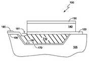
- FIG. 2is a drawing of an electronic device 100 as described in various representative embodiments.
- the electronic device 100is shown as thin film bulk acoustic resonator (FBAR) 100 , also referred to herein as resonator 100 .
- FBARthin film bulk acoustic resonator
- the electronic device 100could be a radio-frequency (RF) filter 100 , resonator 100 , or other appropriate electronic device 100 .
- RFradio-frequency
- the resonator 100is shown in a side view and is fabricated using semiconductor processing compatible procedures.
- the resonator 100is fabricated on a substrate 105 which could be, for example, a semiconductor 105 such as silicon 105 , a semiconductor wafer 105 such as a silicon wafer 105 , a ceramic substrate 105 , or other appropriate substrate material.
- the resonator 100is fabricated above a cavity 110 which isolates the vibrating part of the resonator 100 from the substrate 105 in order to reduce the vibrational energy that would otherwise be dissipated in the substrate 105 .
- the cavity 110is created on the top surface 106 of the substrate 105 .
- the resonator 100is fabricated above and bridges the cavity 110 .
- the resonator 100includes a first electrode 120 also referred to herein as a bottom electrode 120 , a second electrode 130 also referred to herein as a top electrode 130 , and a dielectric layer 140 which in FIG. 2 is piezoelectric layer 140 .
- the piezoelectric layer 140lies generally over at least a part of the bottom electrode 120
- the top electrode 130lies generally over at least part of the piezoelectric layer 140 .
- the coating layer 150lies over at least part of the substrate 105 and lies generally between the substrate 105 and the cavity 110 .
- the coating layer 150can substantially insulate the resonator 100 from susceptibility to parasitic conducting paths that could otherwise occur at the substrate surface 170 in the region of the cavity 110 .
- parasitic conducting pathscan be enabled by the diffusion or deposition of phosphorous from a phosphorous silica glass sacrificial layer lightly doping the walls and surfaces of the depression during processing.
- the materials comprising the coating layer 150 which will reduce, mitigate, or eliminate the leakage conductioncould be various ceramics, dielectrics, metals, and other conductive materials.
- a dielectric materialsuch as silicon dioxide or silicon nitride, or a conductive or semiconductor material, such as aluminum nitride, molybdenum, or gold, could be used.
- FIG. 3is a drawing of another electronic device 100 as described in various representative embodiments.
- the electronic device 100is shown as thin film bulk acoustic resonator (FBAR) 100 .
- FBARthin film bulk acoustic resonator
- the resonator 100is shown in a side view and is fabricated using semiconductor processing compatible procedures.
- the resonator 100is fabricated on the substrate 105 which could be, for example, a semiconductor 105 such as silicon 105 , a semiconductor wafer 105 such as a silicon wafer 105 , a ceramic substrate 105 , or other appropriate substrate material.
- the resonator 100is fabricated above the cavity 110 which isolates the vibrating part of the resonator 100 from the substrate 105 in order to reduce the vibrational energy that would otherwise be dissipated in the substrate 105 .
- the cavity 110is created on the top surface 106 of the substrate 105 .
- the resonator 100is fabricated above and bridges the cavity 110 .
- the resonator 100includes the bottom electrode 120 , the top electrode 130 , and the dielectric layer 140 which in FIG. 3 is piezoelectric layer 140 .
- the piezoelectric layer 140lies generally over at least a part of the bottom electrode 120
- the top electrode 130lies generally over at least part of the piezoelectric layer 140 .
- the coating layer 150lies over at least part of the substrate 105 and lies generally between the substrate 105 and the cavity 110 .
- the coating layer 150can substantially insulate the resonator 100 from parasitic conducting paths that could otherwise occur at the substrate surface 170 in the region of the cavity 110 .
- parasitic conducting pathscan be enabled by the diffusion or deposition of phosphorous from a phosphorous silica glass sacrificial layer lightly doping the walls and surfaces of the depression during processing.
- the materials comprising the coating layer 150 which will reduce, mitigate, or eliminate the leakage conductioncould be various ceramics, dielectrics, metals, and other conductive materials.
- a dielectric materialsuch as silicon dioxide or silicon nitride, or a conductive or semiconductor material, such as aluminum nitride, molybdenum, or gold, could be used.
- the coating layer 150extends beyond the region of the cavity 110 .
- the coating layer 150can thereby be connected to a fixed potential which could be ground. Such grounding could be effected via grounding contact 180 , also referred to herein as contact 180 .
- the electronic device 100comprises a grounding contact 180 that is buried and does not make contact with the coating layer 150 through the release hole.
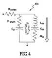
- FIG. 4is a drawing of an equivalent circuit 400 for a thin film bulk acoustic resonator (FBAR).
- Thin film bulk acoustic resonatorscan be used in various representative embodiments herein due to the fact that their fabrication technology is compatible with that of integrated circuits and other semiconductor devices resulting in relative advantages in cost, reliability, and size over other technologies.
- FIG. 4is a modified Butterworth-Van Dyke model of a thin film bulk acoustic resonator. From this equivalent circuit 400 it can be observed that the thin film bulk acoustic resonator has two resonant frequencies. The first resonant frequency is referred to as series resonant frequency f SER which results from the series combination of inductor L M and capacitor C M .
- the second resonant frequencyis referred to as parallel resonant frequency f PAR which results from the parallel combination of shunt capacitor C P and the above series combination of inductor L M and capacitor C M .
- the parallel resonant frequency f PARis also referred to as the anti-resonant frequency f PAR .
- Resistor R SERIES and shunt resistor R SHUNTrepresent non-ideal, resistive components in the structure. With appropriate choice of parameters, combinations of thin film bulk acoustic resonators can be constructed to form a filter that has appropriate bandpass characteristics for a desired filter application.
- FIG. 5is a drawing of a stage in the fabrication of the resonators 100 of FIGS. 1 and 2 .
- the structureis shown in a side view and is fabricated using semiconductor processing compatible procedures.
- the cavity 110can be formed in the substrate 105 by the spinning of photoresist onto the substrate 105 ; the photoresist could be exposed through a photomask having the appropriate pattern; the photoresist could be subsequently developed to appropriately pattern the photoresist; the silicon substrate could be etched using the patterned photoresist as a mask and using well know etching technologies to appropriately pattern the cavity 110 , and then the remaining photoresist could be removed.
- FIG. 6Ais a drawing of another stage in the fabrication of the resonators 100 of FIGS. 1 and 2 .
- the structureis shown in a side view and is fabricated using semiconductor processing compatible procedures.
- the cavity 110 created in FIG. 5is coated with the coating layer 150 .
- the coating layer 150can be added using well known technologies such as chemical vapor deposition, evaporation, or sputtering.
- a layer of a dielectric materialsuch as silicon dioxide or silicon nitride, or a conductive or semiconductor material, such as aluminum nitride, molybdenum, or gold, could be deposited or sputtered onto the top surface 106 including the substrate surface 170 .
- FIG. 6Bis a drawing of a representative embodiment of the coating layer 150 of FIGS. 1 , 2 , and 6 A.
- the coating layer 150comprises a first layer 151 overlaying at least part of the substrate surface 170 in the cavity 110 and a second layer 152 overlying the first layer 151 .
- the first layer 151could comprise silicon dioxide, silicon nitride, polysilicon, or other appropriate material
- the second layer 152could comprise aluminum nitride or other appropriate material.
- FIG. 6Cis a drawing of another representative embodiment of the coating layer 150 of FIGS. 1 , 2 , and 6 A.
- the coating layer 150comprises multiple other layers 153 which could comprise a first layer 151 overlaying at least part of the substrate surface 170 in the cavity 110 and a second layer 152 overlying the first layer 151 .
- the first layer 151could comprise silicon dioxide, silicon nitride, polysilicon, or other appropriate material
- the second layer 152could comprise aluminum nitride or other appropriate material.
- Other layers 153could overlie the second layer 152 .
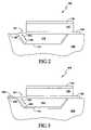
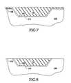
- FIG. 7is a drawing of still another stage in the fabrication of the resonators 100 of FIGS. 1 and 2 .
- the structureis shown in a side view and is fabricated using semiconductor processing compatible procedures.
- the cavity 110 remaining after the addition of the coating layer 150is filled with a sacrificial material 710 which also covers other parts of the top surface 106 of the substrate 105 .
- the sacrificial material 710can be removed later and could be, for example, a phosphorous silica glass material (8% phosphorous, 92% silicon dioxide) which is deposited by chemical vapor deposition.
- FIG. 8is a drawing of still yet another stage in the fabrication of the resonators 100 of FIGS. 1 and 2 .
- the structureis shown in a side view and is fabricated using semiconductor processing compatible procedures.
- the top surface 106 of the substrate 105 and the sacrificial material 710 filled cavity 110are flattened and smoothed via one of a number of well known chemical-mechanical polishing (CMP) processes.
- CMPchemical-mechanical polishing
- FIG. 9is a drawing of a stage in the fabrication of the resonator 100 of FIG. 2 .
- the structureis shown in a side view and is fabricated using semiconductor processing compatible procedures.
- the bottom electrode 120is created above the sacrificial material 710 which along with the coating layer 150 now fills the cavity 110 .
- the bottom electrode 120can be fabricated using well known technologies such as deposition, photolithography, and etch.
- a layer of molybdenumcould be deposited onto the wafer 105 and over the sacrificial material in the cavity 110 followed by the spinning of photoresist onto the wafer 105 ; the photoresist could be exposed through a photomask having the appropriate pattern; the photoresist could be subsequently developed to appropriately pattern the photoresist; the exposed material of the bottom electrode 120 could be etched to appropriately pattern the bottom electrode 120 ; and then the remaining photoresist could be removed.
- the contact 180could be created at the same time as the bottom electrode 120 by patterning the contact 180 to overlap the exposed edge of the coating layer 150 at location 980 .
- a more reliable contactcould be created by inserting an additional processing step to remove the sacrificial material 710 in the vicinity of the release opening 161 exposing that part of the coating layer 150 .
- FIG. 10is a drawing of another stage in the fabrication of the resonator 100 of FIG. 2 .
- the structureis shown in a side view and is fabricated using semiconductor processing compatible procedures.
- the piezoelectric layer 140is created above the bottom electrode 120 .
- the piezoelectric layer 140can be fabricated using well known technologies such as deposition, photolithography, and etch.
- a layer of aluminum nitridecould be deposited onto the wafer 105 and over the bottom electrode 120 followed by the spinning of photoresist onto the wafer 105 ; the photoresist could be exposed through a photomask having the appropriate pattern; the photoresist could be subsequently developed to appropriately pattern the photoresist; the exposed material of the piezoelectric layer 140 could be etched to appropriately pattern the piezoelectric layer 140 ; and then the remaining photoresist could be removed.
- FIG. 11is a drawing of yet another stage in the fabrication of the resonator 100 of FIG. 2 .
- the structureis shown in a side view and is fabricated using semiconductor processing compatible procedures.
- the top electrode 130is created above the piezoelectric layer 140 .
- the top electrode 130can be fabricated using well known technologies such as deposition, photolithography, and etch.
- a layer of molybdenumcould be deposited onto the wafer 105 and over the piezoelectric layer 140 followed by the spinning of photoresist onto the wafer 105 ; the photoresist could be exposed through a photomask having the appropriate pattern; the photoresist could be subsequently developed to appropriately pattern the photoresist; the exposed material of the top electrode 130 could be etched to appropriately pattern the top electrode 130 ; and then the remaining photoresist could be removed.
- the sacrificial material 710 previously deposed in the cavity 110is then removed through the release channel 160 via the release opening 161 to result in the resonator 100 shown in FIG. 2 .
- the location of the release channel 160 in FIG. 11 and other applicable figurescan be inferred from its location in FIGS. 1 and 2 . Should the sacrificial material 710 be a glass, hydrofluoric acid can be used to etch it from the cavity 110 .
- FIG. 12is a drawing of a stage in the fabrication of the resonator 100 of FIG. 3 .
- the structureis shown in a side view and is fabricated using semiconductor processing compatible procedures.
- a contact opening 190is created in a part of the sacrificial material filling the cavity 110 .
- the contact opening 190is opened down to part of the coating layer 150 .
- the contact opening 190can be fabricated using well known technologies such as photolithography and etch.
- photoresistcan be spun onto the wafer 105 ; the photoresist could be exposed through a photomask having the appropriate pattern; the photoresist could be subsequently developed to appropriately pattern the photoresist; part of the exposed sacrificial material 710 of the cavity 110 could be etched to appropriately create the contact opening 190 ; and then the remaining photoresist could be removed. If the sacrificial material 710 is a phosphorous silica glass material, it can be removed by a timed etch with hydrofluoric acid.
- the material for the contact 180is deposited, patterned, and etched prior to deposition of the phosphorous silica glass sacrificial layer 710 . Then the phosphorous silica glass sacrificial layer 710 is then deposited and the chemical-mechanical polishing process is performed.
- the material for the contact 180could be deposited first followed by deposition of the phosphorous silica glass sacrificial layer 710 and chemical-mechanical polishing of the phosphorous silica glass sacrificial layer 710 . Then the contact 180 is patterned and etched. The material for process. Alternatively, an etch stop layer could be added on top of the contact 180 layer. In some embodiments, the material for the contact 180 could be the same material as that of the coating layer 150 . In still other representative embodiments, the contact 180 could be formed by a lift-off process.
- FIG. 13is a drawing of another stage in the fabrication of the resonator 100 of FIG. 3 .
- the structureis shown in a side view and is fabricated using semiconductor processing compatible procedures.
- the bottom electrode 120is created above the sacrificial material in the cavity 110
- the contact 180is created such that it contacts the coating layer 150 through the contact opening 190 .
- the grounding contact 180is a conductive material.
- the bottom electrode 120 and the grounding contact 180can be fabricated using well known technologies such as deposition, photolithography, and etch.
- a layer of molybdenumcould be deposited onto the wafer 105 and over the sacrificial material 710 in the cavity 110 followed by the spinning of photoresist onto the wafer 105 ; the photoresist could be exposed through a photomask having the appropriate pattern; the photoresist could be subsequently developed to appropriately pattern the photoresist; the exposed material of the bottom electrode 120 and of the grounding contact 180 could be etched to appropriately pattern the bottom electrode 120 and the grounding contact 180 ; and then the remaining photoresist could be removed.
- FIG. 14is a drawing of yet another stage in the fabrication of the resonator 100 of FIG. 3 .
- the structureis shown in a side view and is fabricated using semiconductor processing compatible procedures.
- the piezoelectric layer 140is created above the bottom electrode 120 .
- the piezoelectric layer 140can be fabricated using well known technologies such as deposition, photolithography, and etch.
- a layer of aluminum nitridecould be deposited onto the wafer 105 and over the bottom electrode 120 followed by the spinning of photoresist onto the wafer 105 ; the photoresist could be exposed through a photomask having the appropriate pattern; the photoresist could be subsequently developed to appropriately pattern the photoresist; the exposed material of the piezoelectric layer 140 could be etched to appropriately pattern the piezoelectric layer 140 ; and then the remaining photoresist could be removed.
- FIG. 15is a drawing of still another stage in the fabrication of the resonator 100 of FIG. 3 .
- the structureis shown in a side view and is fabricated using semiconductor processing compatible procedures.
- the top electrode 130is created above the piezoelectric layer 140 .
- the top electrode 130can be fabricated using well known technologies such as deposition, photolithography, and etch.
- a layer of molybdenumcould be deposited onto the wafer 105 and over the piezoelectric layer 140 followed by the spinning of photoresist onto the wafer 105 ; the photoresist could be exposed through a photomask having the appropriate pattern; the photoresist could be subsequently developed to appropriately pattern the photoresist; the exposed material of the top electrode 130 could be etched to appropriately pattern the top electrode 130 ; and then the remaining photoresist could be removed.
- the sacrificial material 710 previously deposed in the cavity 110is then removed to result in the resonator 100 shown in FIG. 3 .
- hydrofluoric acidcan be used to etch it from the cavity 110 .
- FIG. 16is a flow chart of a method 1600 for fabricating the resonator 100 of FIG. 2 .
- the cavity 110is created in the substrate 105 .
- the cavity 110can be fabricated using well known technologies such as photolithography and etch.
- photoresistcould be spun onto the wafer 105 ; the photoresist could be exposed through a photomask having the appropriate pattern; the photoresist could be subsequently developed to appropriately pattern the photoresist; the silicon substrate could be etched using the patterned photoresist as a mask to appropriately pattern the cavity 110 ; and then the remaining photoresist could be removed from the wafer 105 .
- Block 1605then transfers control to block 1610 .
- the cavity 110 created in block 1605is coated with the coating layer 150 .
- the coating layer 150can be added using well known technologies such as chemical vapor deposition or sputtering, photolithography, and etch.
- a layer of a dielectric materialsuch as silicon dioxide or silicon nitride, or a conductive or semiconductor material, such as aluminum nitride, molybdenum, or gold, could be deposited or sputtered onto the wafer 105 and over the cavity 110 followed by the spinning of photoresist onto the wafer 105 ; the photoresist could be exposed through a photomask having the appropriate pattern; the photoresist could be subsequently developed to appropriately pattern the photoresist; the exposed material of the coating layer 150 could be etched to appropriately pattern the coating layer 150 ; and then the remaining photoresist could be removed.
- the coating layer 150may remain un-patterned with unneeded portions of the coating layer 150 removed in block 1615 .
- the remaining cavity 110 above the coating layer 150is filled with a sacrificial material 710 .
- the sacrificial material 710can be removed later and could be a phosphorous silica glass material comprising approximately 8% phosphorous and approximately 92% silicon dioxide.
- the cavity 110can be filled with the sacrificial material 710 using well known technologies such as oxide deposition with subsequent surface polishing and etching to form a smooth surface.
- a layer of phosphorous silica glasscould be deposited onto the wafer 105 followed by a mechanical polishing and chemical etching of the wafer surface to flatten and smooth the surface leaving the phosphorous silica glass in the remaining cavity 110 above the coating layer 150 .
- unneeded portions of the coating layer 150can be removed by the chemical-mechanical polishing process of block 1615 .
- Block 1615then transfers control to block 1625 .
- the bottom electrode 120is created above the sacrificial material 710 in the cavity 110 .
- the bottom electrode 120can be fabricated using well known technologies such as deposition, photolithography, and etch.
- a layer of molybdenumcould be deposited onto the wafer 105 and over the sacrificial material 710 in the cavity 110 followed by the spinning of photoresist onto the wafer 105 ; the photoresist could be exposed through a photomask having the appropriate pattern; the photoresist could be subsequently developed to appropriately pattern the photoresist; the exposed material of the bottom electrode 120 could be etched to appropriately pattern the bottom electrode 120 ; and then the remaining photoresist could be removed.
- Block 1625then transfers control to block 1630 .
- the dielectric layer 140is created above the bottom electrode 120 .
- the piezoelectric layer 140can be fabricated using well known technologies such as deposition, photolithography, and etch.
- a layer of aluminum nitridecould be deposited onto the wafer 105 and over the bottom electrode 120 followed by the spinning of photoresist onto the wafer 105 ; the photoresist could be exposed through a photomask having the appropriate pattern; the photoresist could be subsequently developed to appropriately pattern the photoresist; the exposed material of the piezoelectric layer 140 could be etched to appropriately pattern the piezoelectric layer 140 ; and then the remaining photoresist could be removed.
- Block 1630then transfers control to block 1635 .
- the top electrode 130is created above the piezoelectric layer 140 .
- the top electrode 130can be fabricated using well known technologies such as deposition, photolithography, and etch. As an example a layer of molybdenum could be deposited onto the wafer 105 and over the piezoelectric layer 140 followed by the spinning of photoresist onto the wafer 105 ; the photoresist could be exposed through a photomask having the appropriate pattern; the photoresist could be subsequently developed to appropriately pattern the photoresist; the exposed material of the top electrode 130 could be etched to appropriately pattern the top electrode 130 ; and then the remaining photoresist could be removed.
- Block 1035then transfers control to block 1640 .
- Block 1640the sacrificial material 710 previously deposed in the cavity 110 is removed. Should the sacrificial material 710 be a glass, hydrofluoric acid can be used to etch it from the cavity 110 . Block 1640 then terminates the process.
- FIG. 17is a flow chart of a method 1700 for fabricating the resonator 100 of FIG. 3 .
- the cavity 110is created in the substrate 105 .
- the cavity 110can be fabricated using well known technologies such as photolithography and etch.
- photoresistcan be spun onto the wafer 105 ; the photoresist could be exposed through a photomask having the appropriate pattern; the photoresist could be subsequently developed to appropriately pattern the photoresist; the silicon substrate could be etched using the patterned photoresist as a mask to appropriately create the cavity 110 ; and then the remaining photoresist could be removed from the wafer 105 .
- Block 1705then transfers control to block 1710 .
- the cavity 110 created in block 1705is coated with the coating layer 150 .
- the coating layer 150can be added using well known technologies such as chemical vapor deposition or sputtering, photolithography, and etch.
- a layer of a dielectric materialsuch as silicon dioxide or silicon nitride, or a conductive or semiconductor material, such as aluminum nitride, molybdenum, or gold, could be deposited or sputtered onto the wafer 105 and over the sacrificial material in the cavity 110 followed by the spinning of photoresist onto the wafer 105 ; the photoresist could be exposed through a photomask having the appropriate pattern; the photoresist could be subsequently developed to appropriately pattern the photoresist; the exposed material of the coating layer 150 could be etched to appropriately pattern the coating layer 150 ; and then the remaining photoresist could be removed.
- the coating layer 150may remain un-patterned with unneeded portions of the coating layer 150
- the remaining cavity 110 above the coating layer 150is filled with a sacrificial material 710 .
- the sacrificial material 710can be removed later and could be a phosphorous silica glass material comprising approximately 8% phosphorous and approximately 92% silicon dioxide.
- the cavity 110can be filled with the sacrificial material 710 using well known technologies such as oxide deposition with subsequent surface polishing and etching to form a smooth surface.
- a layer of phosphorous silica glasscould be deposited onto the wafer 105 followed by a mechanical polishing and chemical etching of the wafer surface to flatten and smooth the surface leaving the phosphorous silica glass in the remaining cavity 110 above the coating layer 150 .
- unneeded portions of the coating layer 150can be removed by the chemical-mechanical polishing process of block 1715 .
- Block 1715then transfers control to block 1720 .
- the contact opening 190is created through a part of the sacrificial material 710 in the cavity 110 .
- the contact opening 190can be fabricated using well known technologies such as photolithography and etch.
- a layer of photoresistcould be spun onto the wafer 105 and over the sacrificial material 710 in the cavity 110 ; the photoresist could be exposed through a photomask having the appropriate pattern; the photoresist could be subsequently developed to appropriately pattern the photoresist; the exposed sacrificial material 710 in the cavity 110 could be etched down to the coating layer 150 ; and then the remaining photoresist could be removed.
- Block 1720then transfers control to block 1725 .
- the bottom electrode 120is created above the sacrificial material 710 in the cavity 110 .
- the bottom electrode 120can be fabricated using well known technologies such as deposition, photolithography, and etch.
- a layer of molybdenumcould be deposited onto the wafer 105 and over the sacrificial material 710 in the cavity 110 followed by the spinning of photoresist onto the wafer 105 ; the photoresist could be exposed through a photomask having the appropriate pattern; the photoresist could be subsequently developed to appropriately pattern the photoresist; the exposed material of the bottom electrode 120 could be etched to appropriately pattern the bottom electrode 120 ; and then the remaining photoresist could be removed.
- Block 1725then transfers control to block 1730 .
- the contact 180 to the coating layer 150can be formed simultaneously or separately using a separate deposition, pattern, and etch or a pattern, deposition, and lift-off process.
- the electronic device 100comprises a grounding contact 180 that is buried and does not make contact with the coating layer 150 through the release hole.
- the dielectric layer 140is created above the bottom electrode 120 .
- the piezoelectric layer 140can be fabricated using well known technologies such as deposition, photolithography, and etch.
- a layer of aluminum nitridecould be deposited onto the wafer 105 and over the bottom electrode 120 followed by the spinning of photoresist onto the wafer 105 ; the photoresist could be exposed through a photomask having the appropriate pattern; the photoresist could be subsequently developed to appropriately pattern the photoresist; the exposed material of the piezoelectric layer 140 could be etched to appropriately pattern the piezoelectric layer 140 ; and then the remaining photoresist could be removed.
- Block 1730then transfers control to block 1735 .
- the top electrode 130is created above the piezoelectric layer 140 .
- the top electrode 130can be fabricated using well known technologies such as deposition, photolithography, and etch. As an example a layer of molybdenum could be deposited onto the wafer 105 and over the piezoelectric layer 140 followed by the spinning of photoresist onto the wafer 105 ; the photoresist could be exposed through a photomask having the appropriate pattern; the photoresist could be subsequently developed to appropriately pattern the photoresist; the exposed material of the top electrode 130 could be etched to appropriately pattern the top electrode 130 ; and then the remaining photoresist could be removed.
- Block 1035then transfers control to block 1740 .
- Block 1740the sacrificial material 710 previously deposited in the cavity 110 is removed. Should the sacrificial material 710 be a glass, hydrofluoric acid can be used to etch it from the cavity 110 . Block 1740 then terminates the process.
- the bottom electrode 120 , the piezoelectric layer 140 , and the top electrode 130are shown as shortened or truncated over the cavity 110 so that release openings 161 are not covered by these layers which enables making contact to the coating layer 150 and in removing the sacrificial material from the cavity 110 .
- interconnections to the bottom electrode 120 , the grounding contact 180 if present, and the top electrode 130 , as well as various passivation layersare not shown.
- the coating layer 150 , the grounding contact 180 , the bottom electrode 120 , and the top electrode 130may be formed by implanting various materials.
- a buried metallizationmay be formed underneath the wafer surface, followed by deposition of an etch stop layer. Contact to these buried metal layers may be made through vias and via metallization.
- the bottom electrode 120may not make good electrical contact with the substrate 105 as indicated in FIGS. 1-2 , 9 - 11 , and 13 - 15 and associated discussions but may instead be separated from the substrate 105 by an insulating layer which could be, for example, a dielectric layer situated between the bottom electrode 120 and the substrate 105 . However, in such embodiments, the bottom electrode 120 may still be coupled electrically to the substrate 105 via capacitive coupling or inductive coupling.
- the effectiveness of conductive, leakage paths between an electronic device 100 and other additional electronic components 300 on a semiconductor substrate 105 or other applicable substrate 105 materialcan be reduced, mitigated, or eliminated by depositing a selected material that reduces the electrical conduction characteristics in the vicinity of the surface of the cavity 110 .
- the electronic device 100could be one of a number of devices including radio-frequency devices and film bulk acoustic resonators.
Landscapes
- Physics & Mathematics (AREA)
- Acoustics & Sound (AREA)
- Engineering & Computer Science (AREA)
- Manufacturing & Machinery (AREA)
- Piezo-Electric Or Mechanical Vibrators, Or Delay Or Filter Circuits (AREA)
Abstract
Description
Parasitic leakage effects in electronic circuits and devices can result in unwanted and often detrimental spurious signals. Modern devices have become more and more sophisticated with the associated requirement for improved performance with respect to parasitic effects, as well as other performance characteristics, in amplifier and receiver circuits used, for example, in microwave and radio frequency (RF) applications.
RF filter devices built on semiconductor substrates, such as film-bulk acoustic resonators (FBARs), can be susceptible to leakage effects between traces and pads, especially between input and output pads due to intimate connection between the pads and the underlying semiconductor. FBARs manufactured in the manner of an acoustic resonator suspended over a cavity are also susceptible to leakage paths along the floor and walls of the cavity. Extraneous conduction paths can result in multiple deleterious effects, such as poor passband performance. Different types of conduction paths may exist, for example, substrate and surface conduction paths.
In a representative embodiment, an electronic device is disclosed. The electronic device comprises a first electrode and a coating layer. The electronic device is fabricated on a substrate; the substrate has a cavity created in a top surface of the substrate; and the first electrode is electrically coupled to the substrate. The coating layer coats at least part of a substrate surface in the cavity, and the presence of the coating layer results in a mitigation of at least one parasitic leakage path between the first electrode and an additional electrode fabricated on the substrate.
In another representative embodiment, a thin film bulk acoustic resonator is disclosed. The thin film bulk acoustic resonator comprises a first electrode, a piezoelectric layer overlying at least part of the first electrode, a second electrode overlying at least part of the piezoelectric layer, and a coating layer. The thin film bulk acoustic resonator is fabricated on a substrate; the substrate has a cavity created in a top surface of the substrate; and the coating layer coats at least part of a substrate surface in the cavity.
In still another representative embodiment, an electronic module is disclosed. The electronic module comprises a plurality of electronic devices constructed on a substrate. The substrate has at least one cavity created in a top surface of the substrate; at least part of at least one cavity is coated with a coating layer; and the presence of the coating layer results in a mitigation of at least one parasitic leakage path on the substrate.
In yet another representative embodiment, a method for fabricating an electronic device is disclosed. The method comprises creating a cavity in a top surface of a substrate, creating a coating layer overlying at least part of substrate surface in the cavity, filling the cavity with a sacrificial material, and creating a first electrode. The first electrode is electrically coupled to the substrate, and the presence of the coating layer results in a mitigation of at least one parasitic leakage path between the first electrode and an additional electrode fabricated on the substrate.
Other aspects and advantages of the representative embodiments presented herein will become apparent from the following detailed description, taken in conjunction with the accompanying drawings.
The accompanying drawings provide visual representations which will be used to more fully describe various representative embodiments and can be used by those skilled in the art to better understand them and their inherent advantages. In these drawings, like reference numerals identify corresponding elements.
As shown in the drawings for purposes of illustration, novel electronic devices are disclosed herein which have reduced susceptibility to spurious signals including those from leakage effects. In representative embodiments, the effectiveness of surface conduction in providing leakage paths between the traces and the pads of an electronic device can be reduced, mitigated, or eliminated by depositing a selected material on the surface contributing to the leakage. The electronic device could be one of a number of devices including radiofrequency (RF) devices and film-bulk acoustic resonators (FBARs). In the case of a suspended membrane film-bulk acoustic resonator (FBAR), conduction can occur in the “swimming pool” or depression in the substrate over which the film-bulk acoustic resonator is formed. This parasitic conductive path in that depression could be created, for example, by the diffusion or deposition of phosphorous from a phosphorous silica glass sacrificial layer lightly doping the walls and surfaces of the depression. In representative embodiments, the materials deposited on the substrate reducing the leakage conduction could be various ceramics, dielectrics, metals, and other conductive materials. In particular, a dielectric material, such as silicon dioxide or silicon nitride, or a conductive or semiconductor material, such as aluminum nitride (AlN), molybdenum, or gold, could be used. In some representative embodiments, the material used can be attached to a fixed potential which could be ground potential.
In the following detailed description and in the several figures of the drawings, like elements are identified with like reference numerals.
Also shown inFIG. 2 is acoating layer 150, arelease channel 160, and arelease opening 161. The purpose of therelease channel 160 and therelease opening 161 will be explained in the discussion ofFIG. 11 . Thecoating layer 150 lies over at least part of thesubstrate 105 and lies generally between thesubstrate 105 and thecavity 110. Thecoating layer 150 can substantially insulate theresonator 100 from susceptibility to parasitic conducting paths that could otherwise occur at thesubstrate surface 170 in the region of thecavity 110. Such parasitic conducting paths can be enabled by the diffusion or deposition of phosphorous from a phosphorous silica glass sacrificial layer lightly doping the walls and surfaces of the depression during processing.
In representative embodiments, the materials comprising thecoating layer 150 which will reduce, mitigate, or eliminate the leakage conduction could be various ceramics, dielectrics, metals, and other conductive materials. In particular, a dielectric material, such as silicon dioxide or silicon nitride, or a conductive or semiconductor material, such as aluminum nitride, molybdenum, or gold, could be used.
Also shown inFIG. 3 is thecoating layer 150, therelease channel 160 and therelease opening 161. Again, the purpose of therelease channel 160 and therelease opening 161 will be explained in the discussion which follows ofFIG. 11 . Thecoating layer 150 lies over at least part of thesubstrate 105 and lies generally between thesubstrate 105 and thecavity 110. Thecoating layer 150 can substantially insulate theresonator 100 from parasitic conducting paths that could otherwise occur at thesubstrate surface 170 in the region of thecavity 110. Such parasitic conducting paths can be enabled by the diffusion or deposition of phosphorous from a phosphorous silica glass sacrificial layer lightly doping the walls and surfaces of the depression during processing.
In representative embodiments, the materials comprising thecoating layer 150 which will reduce, mitigate, or eliminate the leakage conduction could be various ceramics, dielectrics, metals, and other conductive materials. In particular, a dielectric material, such as silicon dioxide or silicon nitride, or a conductive or semiconductor material, such as aluminum nitride, molybdenum, or gold, could be used. In the representative embodiment ofFIG. 3 , thecoating layer 150 extends beyond the region of thecavity 110. Thecoating layer 150 can thereby be connected to a fixed potential which could be ground. Such grounding could be effected viagrounding contact 180, also referred to herein ascontact 180.
In another representative embodiment, theelectronic device 100 comprises agrounding contact 180 that is buried and does not make contact with thecoating layer 150 through the release hole.
Thesacrificial material 710 previously deposed in thecavity 110 is then removed through therelease channel 160 via the release opening161 to result in theresonator 100 shown inFIG. 2 . The location of therelease channel 160 inFIG. 11 and other applicable figures can be inferred from its location inFIGS. 1 and 2 . Should thesacrificial material 710 be a glass, hydrofluoric acid can be used to etch it from thecavity 110.
In another representative embodiment, the material for thecontact 180 is deposited, patterned, and etched prior to deposition of the phosphorous silica glasssacrificial layer 710. Then the phosphorous silica glasssacrificial layer 710 is then deposited and the chemical-mechanical polishing process is performed.
In still another representative embodiment, The material for thecontact 180 could be deposited first followed by deposition of the phosphorous silica glasssacrificial layer 710 and chemical-mechanical polishing of the phosphorous silica glasssacrificial layer 710. Then thecontact 180 is patterned and etched. The material for process. Alternatively, an etch stop layer could be added on top of thecontact 180 layer. In some embodiments, the material for thecontact 180 could be the same material as that of thecoating layer 150. In still other representative embodiments, thecontact 180 could be formed by a lift-off process.
Thesacrificial material 710 previously deposed in thecavity 110 is then removed to result in theresonator 100 shown inFIG. 3 . Should thesacrificial material 710 be a glass, hydrofluoric acid can be used to etch it from thecavity 110.
Inblock 1610, thecavity 110 created inblock 1605 is coated with thecoating layer 150. Thecoating layer 150 can be added using well known technologies such as chemical vapor deposition or sputtering, photolithography, and etch. As an example, in a representative embodiment, a layer of a dielectric material, such as silicon dioxide or silicon nitride, or a conductive or semiconductor material, such as aluminum nitride, molybdenum, or gold, could be deposited or sputtered onto thewafer 105 and over thecavity 110 followed by the spinning of photoresist onto thewafer 105; the photoresist could be exposed through a photomask having the appropriate pattern; the photoresist could be subsequently developed to appropriately pattern the photoresist; the exposed material of thecoating layer 150 could be etched to appropriately pattern thecoating layer 150; and then the remaining photoresist could be removed. Alternatively, at this stage thecoating layer 150 may remain un-patterned with unneeded portions of thecoating layer 150 removed inblock 1615.Block 1610 then transfers control to block1615.
Inblock 1615, the remainingcavity 110 above thecoating layer 150 is filled with asacrificial material 710. Thesacrificial material 710 can be removed later and could be a phosphorous silica glass material comprising approximately 8% phosphorous and approximately 92% silicon dioxide. Thecavity 110 can be filled with thesacrificial material 710 using well known technologies such as oxide deposition with subsequent surface polishing and etching to form a smooth surface. As an example, a layer of phosphorous silica glass could be deposited onto thewafer 105 followed by a mechanical polishing and chemical etching of the wafer surface to flatten and smooth the surface leaving the phosphorous silica glass in the remainingcavity 110 above thecoating layer 150. As indicated in the discussion ofblock 1610 unneeded portions of the coating layer150 (those portions outside the cavity110) can be removed by the chemical-mechanical polishing process ofblock 1615.Block 1615 then transfers control to block1625.
Inblock 1625, thebottom electrode 120 is created above thesacrificial material 710 in thecavity 110. Thebottom electrode 120 can be fabricated using well known technologies such as deposition, photolithography, and etch. As an example, a layer of molybdenum could be deposited onto thewafer 105 and over thesacrificial material 710 in thecavity 110 followed by the spinning of photoresist onto thewafer 105; the photoresist could be exposed through a photomask having the appropriate pattern; the photoresist could be subsequently developed to appropriately pattern the photoresist; the exposed material of thebottom electrode 120 could be etched to appropriately pattern thebottom electrode 120; and then the remaining photoresist could be removed.Block 1625 then transfers control to block1630.
Inblock 1630, thedielectric layer 140 is created above thebottom electrode 120. In this example, thepiezoelectric layer 140 can be fabricated using well known technologies such as deposition, photolithography, and etch. As an example, a layer of aluminum nitride could be deposited onto thewafer 105 and over thebottom electrode 120 followed by the spinning of photoresist onto thewafer 105; the photoresist could be exposed through a photomask having the appropriate pattern; the photoresist could be subsequently developed to appropriately pattern the photoresist; the exposed material of thepiezoelectric layer 140 could be etched to appropriately pattern thepiezoelectric layer 140; and then the remaining photoresist could be removed.Block 1630 then transfers control to block1635.
Inblock 1635, thetop electrode 130 is created above thepiezoelectric layer 140. Thetop electrode 130 can be fabricated using well known technologies such as deposition, photolithography, and etch. As an example a layer of molybdenum could be deposited onto thewafer 105 and over thepiezoelectric layer 140 followed by the spinning of photoresist onto thewafer 105; the photoresist could be exposed through a photomask having the appropriate pattern; the photoresist could be subsequently developed to appropriately pattern the photoresist; the exposed material of thetop electrode 130 could be etched to appropriately pattern thetop electrode 130; and then the remaining photoresist could be removed. Block1035 then transfers control to block1640.
Inblock 1640, thesacrificial material 710 previously deposed in thecavity 110 is removed. Should thesacrificial material 710 be a glass, hydrofluoric acid can be used to etch it from thecavity 110.Block 1640 then terminates the process.
As will be known to one skilled in the art, in other representative embodiments, various changes can be made to the above described processes to effect similar structures to those just described.
Inblock 1710, thecavity 110 created inblock 1705 is coated with thecoating layer 150. Thecoating layer 150 can be added using well known technologies such as chemical vapor deposition or sputtering, photolithography, and etch. As an example, in a representative embodiment, a layer of a dielectric material, such as silicon dioxide or silicon nitride, or a conductive or semiconductor material, such as aluminum nitride, molybdenum, or gold, could be deposited or sputtered onto thewafer 105 and over the sacrificial material in thecavity 110 followed by the spinning of photoresist onto thewafer 105; the photoresist could be exposed through a photomask having the appropriate pattern; the photoresist could be subsequently developed to appropriately pattern the photoresist; the exposed material of thecoating layer 150 could be etched to appropriately pattern thecoating layer 150; and then the remaining photoresist could be removed. Alternatively, at this stage thecoating layer 150 may remain un-patterned with unneeded portions of thecoating layer 150 removed inblock 1715.Block 1710 then transfers control to block1715.
Inblock 1715, the remainingcavity 110 above thecoating layer 150 is filled with asacrificial material 710. Thesacrificial material 710 can be removed later and could be a phosphorous silica glass material comprising approximately 8% phosphorous and approximately 92% silicon dioxide. Thecavity 110 can be filled with thesacrificial material 710 using well known technologies such as oxide deposition with subsequent surface polishing and etching to form a smooth surface. As an example, a layer of phosphorous silica glass could be deposited onto thewafer 105 followed by a mechanical polishing and chemical etching of the wafer surface to flatten and smooth the surface leaving the phosphorous silica glass in the remainingcavity 110 above thecoating layer 150. As indicated in the discussion ofblock 1710 unneeded portions of the coating layer150 (those portions outside the cavity110) can be removed by the chemical-mechanical polishing process ofblock 1715.Block 1715 then transfers control to block1720.
Inblock 1720, thecontact opening 190 is created through a part of thesacrificial material 710 in thecavity 110. Thecontact opening 190 can be fabricated using well known technologies such as photolithography and etch. As an example, a layer of photoresist could be spun onto thewafer 105 and over thesacrificial material 710 in thecavity 110; the photoresist could be exposed through a photomask having the appropriate pattern; the photoresist could be subsequently developed to appropriately pattern the photoresist; the exposedsacrificial material 710 in thecavity 110 could be etched down to thecoating layer 150; and then the remaining photoresist could be removed.Block 1720 then transfers control to block1725.
Inblock 1725, thebottom electrode 120 is created above thesacrificial material 710 in thecavity 110. Thebottom electrode 120 can be fabricated using well known technologies such as deposition, photolithography, and etch. As an example, a layer of molybdenum could be deposited onto thewafer 105 and over thesacrificial material 710 in thecavity 110 followed by the spinning of photoresist onto thewafer 105; the photoresist could be exposed through a photomask having the appropriate pattern; the photoresist could be subsequently developed to appropriately pattern the photoresist; the exposed material of thebottom electrode 120 could be etched to appropriately pattern thebottom electrode 120; and then the remaining photoresist could be removed.Block 1725 then transfers control to block1730. Thecontact 180 to thecoating layer 150 can be formed simultaneously or separately using a separate deposition, pattern, and etch or a pattern, deposition, and lift-off process. In another representative embodiment, theelectronic device 100 comprises agrounding contact 180 that is buried and does not make contact with thecoating layer 150 through the release hole.
Inblock 1730, thedielectric layer 140 is created above thebottom electrode 120. In this example, thepiezoelectric layer 140 can be fabricated using well known technologies such as deposition, photolithography, and etch. As an example, a layer of aluminum nitride could be deposited onto thewafer 105 and over thebottom electrode 120 followed by the spinning of photoresist onto thewafer 105; the photoresist could be exposed through a photomask having the appropriate pattern; the photoresist could be subsequently developed to appropriately pattern the photoresist; the exposed material of thepiezoelectric layer 140 could be etched to appropriately pattern thepiezoelectric layer 140; and then the remaining photoresist could be removed.Block 1730 then transfers control to block1735.
Inblock 1735, thetop electrode 130 is created above thepiezoelectric layer 140. Thetop electrode 130 can be fabricated using well known technologies such as deposition, photolithography, and etch. As an example a layer of molybdenum could be deposited onto thewafer 105 and over thepiezoelectric layer 140 followed by the spinning of photoresist onto thewafer 105; the photoresist could be exposed through a photomask having the appropriate pattern; the photoresist could be subsequently developed to appropriately pattern the photoresist; the exposed material of thetop electrode 130 could be etched to appropriately pattern thetop electrode 130; and then the remaining photoresist could be removed. Block1035 then transfers control to block1740.
Inblock 1740, thesacrificial material 710 previously deposited in thecavity 110 is removed. Should thesacrificial material 710 be a glass, hydrofluoric acid can be used to etch it from thecavity 110.Block 1740 then terminates the process.
As will be known to one skilled in the art, in other representative embodiments, various changes can be made to the above described processes to effect similar structures to those just described. Such changes can include the addition of a passivation layer on thetop surface 106 of thewafer 105 which could be, for example, silicon dioxide.
In the representative embodiments of theresonators 100 ofFIGS. 1 and 2 thebottom electrode 120, thepiezoelectric layer 140, and thetop electrode 130 are shown as shortened or truncated over thecavity 110 so thatrelease openings 161 are not covered by these layers which enables making contact to thecoating layer 150 and in removing the sacrificial material from thecavity 110. However, it may be necessary to leave only a small part of the upper surface of thesacrificial material 710 as the release opening161 for therelease channel 160 such that a substantial part of the perimeter of thebottom electrode 120 can be supported by thetop surface 106 of thesubstrate 105. Also, interconnections to thebottom electrode 120, thegrounding contact 180 if present, and thetop electrode 130, as well as various passivation layers are not shown.
In various representative embodiments, thecoating layer 150, thegrounding contact 180, thebottom electrode 120, and thetop electrode 130 may be formed by implanting various materials. In other representative embodiments, a buried metallization may be formed underneath the wafer surface, followed by deposition of an etch stop layer. Contact to these buried metal layers may be made through vias and via metallization.
In various representative embodiments, thebottom electrode 120 may not make good electrical contact with thesubstrate 105 as indicated inFIGS. 1-2 ,9-11, and13-15 and associated discussions but may instead be separated from thesubstrate 105 by an insulating layer which could be, for example, a dielectric layer situated between thebottom electrode 120 and thesubstrate 105. However, in such embodiments, thebottom electrode 120 may still be coupled electrically to thesubstrate 105 via capacitive coupling or inductive coupling.
As disclosed herein, the effectiveness of conductive, leakage paths between anelectronic device 100 and other additionalelectronic components 300 on asemiconductor substrate 105 or otherapplicable substrate 105 material can be reduced, mitigated, or eliminated by depositing a selected material that reduces the electrical conduction characteristics in the vicinity of the surface of thecavity 110. Theelectronic device 100 could be one of a number of devices including radio-frequency devices and film bulk acoustic resonators.
The representative embodiments, which have been described in detail herein, have been presented by way of example and not by way of limitation. It will be understood by those skilled in the art that various changes may be made in the form and details of the described embodiments resulting in equivalent embodiments that remain within the scope of the appended claims.
Claims (7)
1. A thin film bulk acoustic resonator, comprising: a first electrode, wherein the thin film bulk acoustic resonator is fabricated on a substrate and wherein the substrate has a cavity created in a top surface of the substrate; a piezoelectric layer overlying at least part of the first electrode; a second electrode overlying at least part of the piezoelectric layer; a coating layer comprising multiple layers, comprising: a first layer comprising silicon dioxide that overlays at least a part of the substrate surface in the cavity and a second layer comprising aluminum nitride that overlays at least part of the first layer, wherein the coating layer coats at least part of a substrate surface in the cavity.
2. The thin film bulk acoustic resonator as recited inclaim 1 , wherein the presence of the coating layer results in a mitigation of at least one parasitic leakage path between the first electrode and an additional electrode fabricated on the substrate.
3. The thin film bulk acoustic resonator as recited inclaim 1 , wherein the cavity is connected by at least one channel to at least one release opening wherein the at least one release opening enables removal of a sacrificial material, and wherein the coating layer covers at least part of the walls of the at least one channel.
4. The thin film bulk acoustic resonator as recited inclaim 1 , wherein the coating layer material is selected from the group of materials consisting of a dielectric material, a semiconductor material, a conductive material, a metal, a ceramic, an implanted material, silicon dioxide, silicon nitride, aluminum nitride, molybdenum, and gold.
5. The thin film bulk acoustic resonator as recited inclaim 1 , wherein the coating layer is attachable to a fixed electrical potential.
6. The thin film bulk acoustic resonator as recited inclaim 1 , wherein the substrate is selected from the group consisting of a semiconductor, a semiconductor wafer, silicon, a silicon wafer, and a ceramic substrate.
7. The thin film bulk acoustic resonator as recited inclaim 1 , wherein the coating layer further overlies at least a part of the top surface of the substrate.
Priority Applications (2)
| Application Number | Priority Date | Filing Date | Title |
|---|---|---|---|
| US11/373,434US7479685B2 (en) | 2006-03-10 | 2006-03-10 | Electronic device on substrate with cavity and mitigated parasitic leakage path |
| US12/341,122US8080854B2 (en) | 2006-03-10 | 2008-12-22 | Electronic device on substrate with cavity and mitigated parasitic leakage path |
Applications Claiming Priority (1)
| Application Number | Priority Date | Filing Date | Title |
|---|---|---|---|
| US11/373,434US7479685B2 (en) | 2006-03-10 | 2006-03-10 | Electronic device on substrate with cavity and mitigated parasitic leakage path |
Related Child Applications (1)
| Application Number | Title | Priority Date | Filing Date |
|---|---|---|---|
| US12/341,122DivisionUS8080854B2 (en) | 2006-03-10 | 2008-12-22 | Electronic device on substrate with cavity and mitigated parasitic leakage path |
Publications (2)
| Publication Number | Publication Date |
|---|---|
| US20070236310A1 US20070236310A1 (en) | 2007-10-11 |
| US7479685B2true US7479685B2 (en) | 2009-01-20 |
Family
ID=38574623
Family Applications (2)
| Application Number | Title | Priority Date | Filing Date |
|---|---|---|---|
| US11/373,434Expired - Fee RelatedUS7479685B2 (en) | 2006-03-10 | 2006-03-10 | Electronic device on substrate with cavity and mitigated parasitic leakage path |
| US12/341,122Expired - Fee RelatedUS8080854B2 (en) | 2006-03-10 | 2008-12-22 | Electronic device on substrate with cavity and mitigated parasitic leakage path |
Family Applications After (1)
| Application Number | Title | Priority Date | Filing Date |
|---|---|---|---|
| US12/341,122Expired - Fee RelatedUS8080854B2 (en) | 2006-03-10 | 2008-12-22 | Electronic device on substrate with cavity and mitigated parasitic leakage path |
Country Status (1)
| Country | Link |
|---|---|
| US (2) | US7479685B2 (en) |
Cited By (7)
| Publication number | Priority date | Publication date | Assignee | Title |
|---|---|---|---|---|
| US20080186247A1 (en)* | 2006-08-03 | 2008-08-07 | International Business Machines Corporation | VERSATILE Si-BASED PACKAGING WITH INTEGRATED PASSIVE COMPONENTS FOR mmWAVE APPLICATIONS |
| US20100052472A1 (en)* | 2008-08-27 | 2010-03-04 | Murata Manufacturing Co., Ltd. | Electronic component and method for manufacturing electronic component |
| US20100212127A1 (en)* | 2009-02-24 | 2010-08-26 | Habbo Heinze | Process for Adapting Resonance Frequency of a BAW Resonator |
| US20100327701A1 (en)* | 2009-06-30 | 2010-12-30 | Avago Technologies Wireless Ip (Singapore) Pte. Ltd. | Piezoelectric resonator structures having temperature compensation |
| US8409875B2 (en) | 2010-10-20 | 2013-04-02 | Rapid Diagnostek, Inc. | Measurement of binding kinetics with a resonating sensor |
| CN106130498A (en)* | 2016-06-28 | 2016-11-16 | 河海大学常州校区 | FBAR resonator and preparation method thereof |
| US20190097603A1 (en)* | 2017-09-25 | 2019-03-28 | Wisol Co., Ltd. | Air-gap type film bulk acoustic resonator and method of manufacturing the same |
Families Citing this family (4)
| Publication number | Priority date | Publication date | Assignee | Title |
|---|---|---|---|---|
| JP2008099004A (en)* | 2006-10-12 | 2008-04-24 | Rohm Co Ltd | Capacitance type sensor manufacturing method and capacitance type sensor |
| DE112010000688B4 (en)* | 2009-01-29 | 2018-08-02 | Murata Manufacturing Co., Ltd. | Process for the preparation of a composite composite substrate |
| US10873311B2 (en)* | 2017-02-15 | 2020-12-22 | Skyworks Solutions, Inc. | Acoustic resonators with reduced loss characteristics and methods of manufacturing same |
| US10256788B2 (en)* | 2017-03-31 | 2019-04-09 | Avago Technologies International Sales Pte. Limited | Acoustic resonator including extended cavity |
Citations (229)
| Publication number | Priority date | Publication date | Assignee | Title |
|---|---|---|---|---|
| US3174122A (en) | 1960-12-12 | 1965-03-16 | Sonus Corp | Frequency selective amplifier |
| US3189851A (en) | 1962-06-04 | 1965-06-15 | Sonus Corp | Piezoelectric filter |
| US3321648A (en) | 1964-06-04 | 1967-05-23 | Sonus Corp | Piezoelectric filter element |
| US3422371A (en) | 1967-07-24 | 1969-01-14 | Sanders Associates Inc | Thin film piezoelectric oscillator |
| GB1207974A (en) | 1966-11-17 | 1970-10-07 | Clevite Corp | Frequency selective apparatus including a piezoelectric device |
| US3582839A (en) | 1968-06-06 | 1971-06-01 | Clevite Corp | Composite coupled-mode filter |
| US3610969A (en) | 1970-02-06 | 1971-10-05 | Mallory & Co Inc P R | Monolithic piezoelectric resonator for use as filter or transformer |
| US3826931A (en) | 1967-10-26 | 1974-07-30 | Hewlett Packard Co | Dual crystal resonator apparatus |
| US3845402A (en) | 1973-02-15 | 1974-10-29 | Edmac Ass Inc | Sonobuoy receiver system, floating coupler |
| US4084217A (en) | 1977-04-19 | 1978-04-11 | Bbc Brown, Boveri & Company, Limited | Alternating-current fed power supply |
| US4172277A (en) | 1977-02-14 | 1979-10-23 | Compagnie Internationale Pour L'informatique Cii-Honeywell Bull (Societe Anonyme) | Chopping control system for a converter in a DC electrical power supply |
| US4272742A (en) | 1978-09-22 | 1981-06-09 | The Secretary Of State For Defence In Her Britannic Majesty's Government Of The United Kingdom Of Great Britain And Northern Ireland | Acoustic wave devices with temperature stabilization |
| US4281299A (en) | 1979-11-23 | 1981-07-28 | Honeywell Inc. | Signal isolator |
| US4320365A (en) | 1980-11-03 | 1982-03-16 | United Technologies Corporation | Fundamental, longitudinal, thickness mode bulk wave resonator |
| US4355408A (en) | 1980-02-13 | 1982-10-19 | International Computers Limited | System for extracting timing information from a digital waveform |
| US4456850A (en) | 1982-02-09 | 1984-06-26 | Nippon Electric Co., Ltd. | Piezoelectric composite thin film resonator |
| US4529904A (en) | 1983-03-16 | 1985-07-16 | International Standard Electric Corporation | Piezo-electric terminal station for communications system |
| JPS6154686B2 (en) | 1982-10-06 | 1986-11-25 | Hitachi Ltd | |
| US4625138A (en) | 1984-10-24 | 1986-11-25 | The United States Of America As Represented By The Secretary Of The Army | Piezoelectric microwave resonator using lateral excitation |
| US4640756A (en) | 1983-10-25 | 1987-02-03 | The United States Of America As Represented By The United States Department Of Energy | Method of making a piezoelectric shear wave resonator |
| EP0231892A2 (en) | 1986-01-31 | 1987-08-12 | Showa Electric Wire & Cable Co.,Ltd. | Electric signal transfer element |
| US4719383A (en) | 1985-05-20 | 1988-01-12 | The United States Of America As Represented By The United States Department Of Energy | Piezoelectric shear wave resonator and method of making same |
| US4798990A (en) | 1986-09-11 | 1989-01-17 | Bengt Henoch | Device for transmitting electric energy to computers and data nets |
| US4836882A (en) | 1988-09-12 | 1989-06-06 | The United States Of America As Represented By The Secretary Of The Army | Method of making an acceleration hardened resonator |
| US4841429A (en) | 1988-03-24 | 1989-06-20 | Hughes Aircraft Company | Capacitive coupled power supplies |
| US4906840A (en) | 1988-01-27 | 1990-03-06 | The Board Of Trustees Of Leland Stanford Jr., University | Integrated scanning tunneling microscope |
| US5048038A (en) | 1990-01-25 | 1991-09-10 | The United States Of America As Represented By The United States Department Of Energy | Ion-implanted planar-buried-heterostructure diode laser |
| US5048036A (en) | 1989-09-18 | 1991-09-10 | Spectra Diode Laboratories, Inc. | Heterostructure laser with lattice mismatch |
| US5075641A (en) | 1990-12-04 | 1991-12-24 | Iowa State University Research Foundation, Inc. | High frequency oscillator comprising cointegrated thin film resonator and active device |
| US5118982A (en) | 1989-05-31 | 1992-06-02 | Nec Corporation | Thickness mode vibration piezoelectric transformer |
| US5162691A (en) | 1991-01-22 | 1992-11-10 | The United States Of America As Represented By The Secretary Of The Army | Cantilevered air-gap type thin film piezoelectric resonator |
| US5241456A (en) | 1990-07-02 | 1993-08-31 | General Electric Company | Compact high density interconnect structure |
| US5241209A (en) | 1990-07-24 | 1993-08-31 | Fujitsu Limited | Semi-conductor device having circuits on both sides of insulation layer and ultrasonic signal path between the circuits |
| US5294898A (en) | 1992-01-29 | 1994-03-15 | Motorola, Inc. | Wide bandwidth bandpass filter comprising parallel connected piezoelectric resonators |
| US5361077A (en) | 1992-05-29 | 1994-11-01 | Iowa State University Research Foundation, Inc. | Acoustically coupled antenna utilizing an overmoded configuration |
| US5382930A (en) | 1992-12-21 | 1995-01-17 | Trw Inc. | Monolithic multipole filters made of thin film stacked crystal filters |
| US5384808A (en) | 1992-12-31 | 1995-01-24 | Apple Computer, Inc. | Method and apparatus for transmitting NRZ data signals across an isolation barrier disposed in an interface between adjacent devices on a bus |
| EP0637875A1 (en) | 1993-08-04 | 1995-02-08 | Motorola, Inc. | Acoustical isolator and method therefor |
| US5448014A (en) | 1993-01-27 | 1995-09-05 | Trw Inc. | Mass simultaneous sealing and electrical connection of electronic devices |
| US5465725A (en) | 1993-06-15 | 1995-11-14 | Hewlett Packard Company | Ultrasonic probe |
| EP0689254A1 (en) | 1994-06-23 | 1995-12-27 | Motorola, Inc. | Accoustic isolator |
| US5587620A (en) | 1993-12-21 | 1996-12-24 | Hewlett-Packard Company | Tunable thin film acoustic resonators and method for making the same |
| US5589858A (en) | 1990-05-22 | 1996-12-31 | Canon Kabushiki Kaisha | Information recording apparatus |
| US5594705A (en) | 1994-02-04 | 1997-01-14 | Dynamotive Canada Corporation | Acoustic transformer with non-piezoelectric core |
| US5671242A (en) | 1994-09-02 | 1997-09-23 | Mitsubishi Denki Kabushiki Kaisha | Strained quantum well structure |
| US5692279A (en) | 1995-08-17 | 1997-12-02 | Motorola | Method of making a monolithic thin film resonator lattice filter |
| US5705877A (en) | 1995-10-12 | 1998-01-06 | Nec Corporation | Piezoelectric transformer driving circuit |
| US5714917A (en) | 1996-10-02 | 1998-02-03 | Nokia Mobile Phones Limited | Device incorporating a tunable thin film bulk acoustic resonator for performing amplitude and phase modulation |
| WO1998016957A1 (en) | 1996-10-17 | 1998-04-23 | Nokia Mobile Phones Limited | A resonator having an acoustic mirror |
| US5853601A (en) | 1997-04-03 | 1998-12-29 | Northrop Grumman Corporation | Top-via etch technique for forming dielectric membranes |
| US5864261A (en) | 1994-05-23 | 1999-01-26 | Iowa State University Research Foundation | Multiple layer acoustical structures for thin-film resonator based circuits and systems |
| US5866969A (en) | 1996-10-24 | 1999-02-02 | Nec Corporation | Actuating circuit of piezoelectric transformer and actuating method thereof |
| US5872493A (en) | 1997-03-13 | 1999-02-16 | Nokia Mobile Phones, Ltd. | Bulk acoustic wave (BAW) filter having a top portion that includes a protective acoustic mirror |
| US5894184A (en) | 1996-08-01 | 1999-04-13 | Nec Corporation | Drive circuit for driving a piezoelectric transformer capable of decreasing heat developed from electronic parts composing an inverter circuit |
| US5894647A (en) | 1997-06-30 | 1999-04-20 | Tfr Technologies, Inc. | Method for fabricating piezoelectric resonators and product |
| US5910756A (en) | 1997-05-21 | 1999-06-08 | Nokia Mobile Phones Limited | Filters and duplexers utilizing thin film stacked crystal filter structures and thin film bulk acoustic wave resonators |
| US5932953A (en) | 1997-06-30 | 1999-08-03 | Iowa State University Research Foundation, Inc. | Method and system for detecting material using piezoelectric resonators |
| US5936150A (en) | 1998-04-13 | 1999-08-10 | Rockwell Science Center, Llc | Thin film resonant chemical sensor with resonant acoustic isolator |
| US5953479A (en) | 1998-05-07 | 1999-09-14 | The United States Of America As Represented By The Secretary Of The Army | Tilted valance-band quantum well double heterostructures for single step active and passive optical waveguide device monolithic integration |
| US5982297A (en) | 1997-10-08 | 1999-11-09 | The Aerospace Corporation | Ultrasonic data communication system |
| US6040962A (en) | 1997-05-14 | 2000-03-21 | Tdk Corporation | Magnetoresistive element with conductive films and magnetic domain films overlapping a central active area |
| US6060818A (en) | 1998-06-02 | 2000-05-09 | Hewlett-Packard Company | SBAR structures and method of fabrication of SBAR.FBAR film processing techniques for the manufacturing of SBAR/BAR filters |
| US6087198A (en) | 1998-02-12 | 2000-07-11 | Texas Instruments Incorporated | Low cost packaging for thin-film resonators and thin-film resonator-based filters |
| US6107721A (en) | 1999-07-27 | 2000-08-22 | Tfr Technologies, Inc. | Piezoelectric resonators on a differentially offset reflector |
| US6111480A (en) | 1997-07-07 | 2000-08-29 | Murata Manfacturing Co., Ltd. | Piezoelectric resonator and method of adjusting resonant frequency thereof |
| US6124756A (en) | 1996-04-08 | 2000-09-26 | Texas Instruments Incorporated | Method and apparatus for galvanically isolating two integrated circuits from each other |
| US6150703A (en) | 1998-06-29 | 2000-11-21 | Trw Inc. | Lateral mode suppression in semiconductor bulk acoustic resonator (SBAR) devices using tapered electrodes, and electrodes edge damping materials |
| WO2001006647A1 (en) | 1999-07-19 | 2001-01-25 | Nokia Corporation | Resonator structure and a filter comprising such a resonator structure |
| US6187513B1 (en) | 1998-05-29 | 2001-02-13 | Sony Corporation | Process for forming mask pattern and process for producing thin film magnetic head |
| US6215375B1 (en) | 1999-03-30 | 2001-04-10 | Agilent Technologies, Inc. | Bulk acoustic wave resonator with improved lateral mode suppression |
| US6228675B1 (en) | 1999-07-23 | 2001-05-08 | Agilent Technologies, Inc. | Microcap wafer-level package with vias |
| US6229247B1 (en) | 1998-11-09 | 2001-05-08 | Face International Corp. | Multi-layer piezoelectric electrical energy transfer device |
| US6252229B1 (en) | 1998-07-10 | 2001-06-26 | Boeing North American, Inc. | Sealed-cavity microstructure and microbolometer and associated fabrication methods |
| US6262637B1 (en) | 1999-06-02 | 2001-07-17 | Agilent Technologies, Inc. | Duplexer incorporating thin-film bulk acoustic resonators (FBARs) |
| US6262600B1 (en) | 2000-02-14 | 2001-07-17 | Analog Devices, Inc. | Isolator for transmitting logic signals across an isolation barrier |
| US6265246B1 (en) | 1999-07-23 | 2001-07-24 | Agilent Technologies, Inc. | Microcap wafer-level package |
| US6278342B1 (en) | 1998-12-30 | 2001-08-21 | Nokia Mobile Phones, Ltd. | Balanced filter structure utilizing bulk acoustic wave resonators having different areas |
| US6292336B1 (en) | 1999-09-30 | 2001-09-18 | Headway Technologies, Inc. | Giant magnetoresistive (GMR) sensor element with enhanced magnetoresistive (MR) coefficient |
| EP1047189A3 (en) | 1999-04-19 | 2001-09-19 | Murata Manufacturing Co., Ltd. | Piezoelectric resonator |
| US6307447B1 (en) | 1999-11-01 | 2001-10-23 | Agere Systems Guardian Corp. | Tuning mechanical resonators for electrical filter |
| US6307761B1 (en) | 1998-03-23 | 2001-10-23 | Fidelix Y.K. | Single stage high power-factor converter |
| WO2001099276A1 (en) | 2000-06-20 | 2001-12-27 | Koninklijke Philips Electronics N.V. | A bulk acoustic wave device |
| US20020000646A1 (en) | 2000-02-02 | 2002-01-03 | Raytheon Company, A Delware Corporation | Vacuum package fabrication of integrated circuit components |
| US20020030424A1 (en) | 1999-12-22 | 2002-03-14 | Toyo Communication Equipment Co., Ltd. | High frequency piezoelectric resonator |
| US6366006B1 (en) | 2000-12-15 | 2002-04-02 | Clark Davis Boyd | Composite piezoelectric transformer |
| US6377137B1 (en) | 2000-09-11 | 2002-04-23 | Agilent Technologies, Inc. | Acoustic resonator filter with reduced electromagnetic influence due to die substrate thickness |
| US6384697B1 (en)* | 2000-05-08 | 2002-05-07 | Agilent Technologies, Inc. | Cavity spanning bottom electrode of a substrate-mounted bulk wave acoustic resonator |
| US6407649B1 (en) | 2001-01-05 | 2002-06-18 | Nokia Corporation | Monolithic FBAR duplexer and method of making the same |
| US6414569B1 (en) | 1999-11-01 | 2002-07-02 | Murata Manufacturing Co., Ltd. | Method of adjusting frequency of piezoelectric resonance element by removing material from a thicker electrode or adding, material to a thinner electrode |
| US6420820B1 (en) | 2000-08-31 | 2002-07-16 | Agilent Technologies, Inc. | Acoustic wave resonator and method of operating the same to maintain resonance when subjected to temperature variations |
| US6424237B1 (en) | 2000-12-21 | 2002-07-23 | Agilent Technologies, Inc. | Bulk acoustic resonator perimeter reflection system |
| JP2002217676A (en) | 2001-01-17 | 2002-08-02 | Murata Mfg Co Ltd | Piezoelectric filter |
| US6429511B2 (en) | 1999-07-23 | 2002-08-06 | Agilent Technologies, Inc. | Microcap wafer-level package |
| US6434030B1 (en) | 1998-06-12 | 2002-08-13 | Thomas Licensing Sa | Arrangement having a switched-mode power supply and a microprocessor |
| US6441539B1 (en) | 1999-11-11 | 2002-08-27 | Murata Manufacturing Co., Ltd. | Piezoelectric resonator |
| US20020121945A1 (en) | 2001-03-05 | 2002-09-05 | Ruby Richard C. | Method of mass loading of thin film bulk acoustic resonators (fbar) for creating resonators of different frequencies and apparatus embodying the method |
| US20020121944A1 (en) | 2001-03-05 | 2002-09-05 | Larson John D. | Method of providing differential frequency adjusts in a thin film bulk acoustic resonator (FBAR) filter and apparatus embodying the method |
| US6462631B2 (en) | 2001-02-14 | 2002-10-08 | Agilent Technologies, Inc. | Passband filter having an asymmetrical filter response |
| US6466418B1 (en) | 2000-02-11 | 2002-10-15 | Headway Technologies, Inc. | Bottom spin valves with continuous spacer exchange (or hard) bias |
| US6466105B1 (en) | 1999-07-07 | 2002-10-15 | Koninklijke Philips Electronics N.V. | Bulk acoustic wave filter |
| US20020152803A1 (en) | 2001-04-23 | 2002-10-24 | Larson John D. | Systems and methods of monitoring thin film deposition |
| US6472954B1 (en) | 2001-04-23 | 2002-10-29 | Agilent Technologies, Inc. | Controlled effective coupling coefficients for film bulk acoustic resonators |
| US6476536B1 (en) | 2001-04-27 | 2002-11-05 | Nokia Corporation | Method of tuning BAW resonators |
| US6479320B1 (en) | 2000-02-02 | 2002-11-12 | Raytheon Company | Vacuum package fabrication of microelectromechanical system devices with integrated circuit components |
| US6483229B2 (en) | 2001-03-05 | 2002-11-19 | Agilent Technologies, Inc. | Method of providing differential frequency adjusts in a thin film bulk acoustic resonator (FBAR) filter and apparatus embodying the method |
| US6486751B1 (en) | 2000-09-26 | 2002-11-26 | Agere Systems Inc. | Increased bandwidth thin film resonator having a columnar structure |
| US6489688B1 (en) | 2001-05-02 | 2002-12-03 | Zeevo, Inc. | Area efficient bond pad placement |
| US6492883B2 (en) | 2000-11-03 | 2002-12-10 | Paratek Microwave, Inc. | Method of channel frequency allocation for RF and microwave duplexers |
| US20020190814A1 (en) | 2001-05-11 | 2002-12-19 | Tetsuo Yamada | Thin film bulk acoustic resonator and method of producing the same |
| WO2002103900A1 (en) | 2001-06-15 | 2002-12-27 | Ube Electronics, Ltd. | Thin-film piezoelectric resonator |
| US20030001251A1 (en) | 2001-01-10 | 2003-01-02 | Cheever James L. | Wafer level interconnection |
| US20030006502A1 (en) | 2000-04-10 | 2003-01-09 | Maurice Karpman | Hermetically sealed microstructure package |
| US6515558B1 (en) | 2000-11-06 | 2003-02-04 | Nokia Mobile Phones Ltd | Thin-film bulk acoustic resonator with enhanced power handling capacity |
| US6518860B2 (en) | 2001-01-05 | 2003-02-11 | Nokia Mobile Phones Ltd | BAW filters having different center frequencies on a single substrate and a method for providing same |
| US6525996B1 (en) | 1998-12-22 | 2003-02-25 | Seiko Epson Corporation | Power feeding apparatus, power receiving apparatus, power transfer system, power transfer method, portable apparatus, and timepiece |
| US6530515B1 (en) | 2000-09-26 | 2003-03-11 | Amkor Technology, Inc. | Micromachine stacked flip chip package fabrication method |
| US6534900B2 (en) | 2000-02-18 | 2003-03-18 | Infineon Technologies Ag | Piezoresonator |
| US20030051550A1 (en) | 2001-08-16 | 2003-03-20 | Nguyen Clark T.-C. | Mechanical resonator device having phenomena-dependent electrical stiffness |
| US6542055B1 (en) | 2000-10-31 | 2003-04-01 | Agilent Technologies, Inc. | Integrated filter balun |
| WO2003030358A1 (en) | 2001-09-25 | 2003-04-10 | Infineon Technologies Ag | Piezo-electrical component and method for production thereof |
| US6550664B2 (en) | 2000-12-09 | 2003-04-22 | Agilent Technologies, Inc. | Mounting film bulk acoustic resonators in microwave packages using flip chip bonding technology |
| US20030087469A1 (en) | 2001-11-02 | 2003-05-08 | Intel Corporation | Method of fabricating an integrated circuit that seals a MEMS device within a cavity |
| US6564448B1 (en) | 1998-05-08 | 2003-05-20 | Nec Corporation | Resin structure in which manufacturing cost is cheap and sufficient adhesive strength can be obtained and method of manufacturing it |
| WO2003043188A1 (en) | 2001-11-14 | 2003-05-22 | Infineon Technologies Ag | Passivated baw resonator and baw filter |
| US20030102776A1 (en) | 2001-11-29 | 2003-06-05 | Matsushita Electric Industrial Co., Ltd. | Driving circuit for piezoelectric transformer, cold-cathode tube light-emitting apparatus, liquid crystal panel and device with built-in liquid crystal panel |
| DE10160617A1 (en) | 2001-12-11 | 2003-06-12 | Epcos Ag | Acoustic mirror with improved reflection |
| US20030111439A1 (en) | 2001-12-14 | 2003-06-19 | Fetter Linus Albert | Method of forming tapered electrodes for electronic devices |
| US6583374B2 (en) | 2001-02-20 | 2003-06-24 | Rockwell Automation Technologies, Inc. | Microelectromechanical system (MEMS) digital electrical isolator |
| US6583688B2 (en) | 2000-04-06 | 2003-06-24 | Koninklijke Philips Electronics N.V. | Tunable filter arrangement comprising resonators with reflection layers |
| US20030128081A1 (en) | 2002-01-09 | 2003-07-10 | Nokia Corporation | Bulk acoustic wave resonator with two piezoelectric layers as balun in filters and duplexers |
| US6593870B2 (en) | 2001-10-18 | 2003-07-15 | Rockwell Automation Technologies, Inc. | MEMS-based electrically isolated analog-to-digital converter |
| US20030132493A1 (en) | 1999-11-01 | 2003-07-17 | Samsung Electronics Co., Ltd. | High-vacuum packaged microgyroscope and method for manufacturing the same |
| US6600390B2 (en) | 2001-12-13 | 2003-07-29 | Agilent Technologies, Inc. | Differential filters with common mode rejection and broadband rejection |
| US20030141946A1 (en) | 2002-01-31 | 2003-07-31 | Ruby Richard C. | Film bulk acoustic resonator (FBAR) and the method of making the same |
| US6601276B2 (en) | 2001-05-11 | 2003-08-05 | Agere Systems Inc. | Method for self alignment of patterned layers in thin film acoustic devices |
| US6617750B2 (en) | 1999-09-21 | 2003-09-09 | Rockwell Automation Technologies, Inc. | Microelectricalmechanical system (MEMS) electrical isolator with reduced sensitivity to inertial noise |
| US6617249B2 (en) | 2001-03-05 | 2003-09-09 | Agilent Technologies, Inc. | Method for making thin film bulk acoustic resonators (FBARS) with different frequencies on a single substrate and apparatus embodying the method |
| US20030179053A1 (en) | 2001-03-23 | 2003-09-25 | Robert Aigner | Filter device |
| US6630753B2 (en) | 2001-10-29 | 2003-10-07 | International Business Machines Corporation | Low cost redundant AC to DC power supply |
| US6635509B1 (en) | 2002-04-12 | 2003-10-21 | Dalsa Semiconductor Inc. | Wafer-level MEMS packaging |
| US6639872B1 (en) | 1997-12-08 | 2003-10-28 | Claus Rein | Remote energy supply process and system for an electronic information carrier |
| US6657363B1 (en) | 1998-05-08 | 2003-12-02 | Infineon Technologies Ag | Thin film piezoelectric resonator |
| US6693500B2 (en) | 2001-06-25 | 2004-02-17 | Samsung Electro-Mechanics Co., Ltd. | Film bulk acoustic resonator with improved lateral mode suppression |
| US6710681B2 (en) | 2001-07-13 | 2004-03-23 | Agilent Technologies, Inc. | Thin film bulk acoustic resonator (FBAR) and inductor on a monolithic substrate and method of fabricating the same |
| US6710508B2 (en) | 2001-11-27 | 2004-03-23 | Agilent Technologies, Inc. | Method for adjusting and stabilizing the frequency of an acoustic resonator |
| US6714102B2 (en) | 2001-03-01 | 2004-03-30 | Agilent Technologies, Inc. | Method of fabricating thin film bulk acoustic resonator (FBAR) and FBAR structure embodying the method |
| US6720844B1 (en) | 2001-11-16 | 2004-04-13 | Tfr Technologies, Inc. | Coupled resonator bulk acoustic wave filter |
| US6720846B2 (en) | 2001-03-21 | 2004-04-13 | Seiko Epson Corporation | Surface acoustic wave device with KNb03 piezoelectric thin film, frequency filter, oscillator, electronic circuit, and electronic apparatus |
| US6724266B2 (en) | 2000-01-10 | 2004-04-20 | Eta Sa Fabriques D'ebauches | Device for producing a signal having a substantially temperature-independent frequency |
| WO2004034579A1 (en) | 2002-10-08 | 2004-04-22 | Epcos Ag | Bulk acoustic wave resonator and circuit comprising same |
| US20040092234A1 (en) | 2002-11-12 | 2004-05-13 | Nokia Corporation | Crystal-less oscillator transceiver |
| US20040124952A1 (en) | 2002-12-13 | 2004-07-01 | Epcos Ag | Component operating with bulk acoustic waves, and having coupled resonators |
| US20040150296A1 (en) | 2003-01-24 | 2004-08-05 | Lg Electronics Inc. | Material sensing sensor and module using thin film bulk acoustic resonator |
| US20040150293A1 (en) | 2002-12-05 | 2004-08-05 | Michael Unterberger | Component operating with bulk acoustic waves, and having asymmetric/symmetrical circuitry |
| US6774746B2 (en) | 2000-05-24 | 2004-08-10 | Tdk Corporation | Thin film bulk acoustic resonator filters with a piezoelectric layer of lead scandium tantalum oxide |
| US6777263B1 (en) | 2003-08-21 | 2004-08-17 | Agilent Technologies, Inc. | Film deposition to enhance sealing yield of microcap wafer-level package with vias |
| US6787048B2 (en) | 2001-03-05 | 2004-09-07 | Agilent Technologies, Inc. | Method for producing thin bulk acoustic resonators (FBARs) with different frequencies on the same substrate by subtracting method and apparatus embodying the method |
| US20040195937A1 (en) | 2003-04-01 | 2004-10-07 | Shogo Matsubara | Film bulk acoustic resonator and film bulk acoustic resonator circuit |
| US6803835B2 (en) | 2001-08-30 | 2004-10-12 | Agilent Technologies, Inc. | Integrated filter balun |
| US6828713B2 (en) | 2002-07-30 | 2004-12-07 | Agilent Technologies, Inc | Resonator with seed layer |
| US20040257172A1 (en) | 2003-04-17 | 2004-12-23 | Edgar Schmidhammer | Duplexer with extended functionality |
| US20040263287A1 (en) | 2003-06-30 | 2004-12-30 | Eyal Ginsburg | Tapered electrode in an acoustic resonator |
| WO2004051744A3 (en) | 2002-07-25 | 2005-01-13 | Freescale Semiconductor Inc | Mems control chip integration |
| US20050012570A1 (en) | 2003-04-30 | 2005-01-20 | Christian Korden | Component functioning with bulk acoustic waves having coupled resonators |
| US20050023931A1 (en) | 2002-11-28 | 2005-02-03 | Stmicroelectronics S.A. | Support and decoupling structure for an acoustic resonator, acoustic resonator and corresponding integrated circuit |
| US20050030126A1 (en) | 2003-08-04 | 2005-02-10 | Tdk Corporation | Filter device and branching filter using same |
| US20050036604A1 (en) | 1997-04-22 | 2005-02-17 | Silicon Laboratories Inc. | Direct digital access arrangement circuitry and method for connecting DSL circuitry to phone lines |
| EP1249932A3 (en) | 2001-04-12 | 2005-03-02 | Nokia Corporation | Method of producing thin-film bulk acoustic wave devices |
| US20050057117A1 (en) | 2003-09-17 | 2005-03-17 | Hiroshi Nakatsuka | Piezoelectric resonator, filter, and duplexer |
| US20050057324A1 (en) | 2003-09-12 | 2005-03-17 | Keiji Onishi | Thin film bulk acoustic resonator, method for producing the same, filter, composite electronic component device, and communication device |
| US6873529B2 (en) | 2002-02-26 | 2005-03-29 | Kyocera Corporation | High frequency module |
| US6873065B2 (en) | 1997-10-23 | 2005-03-29 | Analog Devices, Inc. | Non-optical signal isolator |
| US6874211B2 (en) | 2001-03-05 | 2005-04-05 | Agilent Technologies, Inc. | Method for producing thin film bulk acoustic resonators (FBARs) with different frequencies on the same substrate by subtracting method and apparatus embodying the method |
| US6888424B2 (en) | 2001-07-03 | 2005-05-03 | Murata Manufacturing Co., Ltd. | Piezoelectric resonator, filter, and electronic communication device |
| EP1528675A1 (en) | 2003-10-30 | 2005-05-04 | Agilent Technologies, Inc. | Thin film acoustically-coupled transformer |
| US20050093655A1 (en) | 2003-10-30 | 2005-05-05 | Larson John D.Iii | Film acoustically-coupled transformer |
| US20050093653A1 (en) | 2003-10-30 | 2005-05-05 | Larson John D.Iii | Stacked bulk acoustic resonator band-pass filter with controllable pass bandwidth |
| WO2005043756A1 (en) | 2003-10-30 | 2005-05-12 | Agilent Technologies, Inc. | Temperature-compensated film bulk acoustic resonator (fbar) devices |
| US6900705B2 (en) | 2002-03-15 | 2005-05-31 | Matsushita Electric Industrial Co., Ltd. | Balanced high-frequency device and balance-characteristics improving method and balanced high-frequency circuit using the same |
| US6903452B2 (en) | 2002-04-03 | 2005-06-07 | Intel Corporation | Packaging microelectromechanical structures |
| US6906451B2 (en) | 2002-01-08 | 2005-06-14 | Murata Manufacturing Co., Ltd. | Piezoelectric resonator, piezoelectric filter, duplexer, communication apparatus, and method for manufacturing piezoelectric resonator |
| US6911708B2 (en) | 2003-02-21 | 2005-06-28 | Lg Electronics Inc. | Duplexer filter having film bulk acoustic resonator and semiconductor package thereof |
| US20050140466A1 (en) | 2003-10-30 | 2005-06-30 | Larson John D.Iii | Decoupled stacked bulk acoustic resonator-based band-pass filter |
| EP1557945A4 (en) | 2002-10-28 | 2005-07-27 | Matsushita Electric Industrial Co Ltd | PIEZOELECTRIC VIBRATOR, FILTER USING SUCH A VIBRATOR, AND METHOD FOR ADJUSTING A PIEZOELECTRIC VIBRATOR |
| US6924583B2 (en) | 2002-05-03 | 2005-08-02 | Asia Pacific Microsystems, Inc. | Film bulk acoustic device with integrated tunable and trimmable device |
| US20050167795A1 (en) | 2002-12-27 | 2005-08-04 | Shinko Electric Industries Co., Ltd. | Electronic devices and its production methods |
| US6927651B2 (en) | 2003-05-12 | 2005-08-09 | Agilent Technologies, Inc. | Acoustic resonator devices having multiple resonant frequencies and methods of making the same |
| US6936928B2 (en) | 2000-03-23 | 2005-08-30 | Infineon Technologies Ag | Semiconductor component and method for its production |
| US6936954B2 (en) | 2001-08-29 | 2005-08-30 | Honeywell International Inc. | Bulk resonator |
| US20050193507A1 (en) | 2004-03-04 | 2005-09-08 | Ludwiczak Damian R. | Vibrating debris remover |
| US20050206271A1 (en) | 2004-03-17 | 2005-09-22 | Takamitsu Higuchi | Potassium niobate deposited body, method for manufacturing the same, piezoelectric thin film resonator, frequency filter, frequency oscillator, electronic circuit, and electronic apparatus |
| US20050218488A1 (en) | 2004-03-31 | 2005-10-06 | Mie Matsuo | Electronic component having micro-electrical mechanical system |
| US6954121B2 (en) | 2003-06-09 | 2005-10-11 | Agilent Technologies, Inc. | Method for controlling piezoelectric coupling coefficient in film bulk acoustic resonators and apparatus embodying the method |
| US6963257B2 (en) | 2004-03-19 | 2005-11-08 | Nokia Corporation | Coupled BAW resonator based duplexers |
| US6970365B2 (en) | 2001-12-12 | 2005-11-29 | Jpmorgan Chase Bank, N.A. | Controlled frequency power factor correction circuit and method |
| US6975183B2 (en) | 2001-10-08 | 2005-12-13 | Infineon Technologies Ag | BAW resonator having piezoelectric layers oriented in opposed directions |
| US6977563B2 (en) | 2002-09-27 | 2005-12-20 | Tdk Corporation | Thin-film piezoelectric resonator and method for fabricating the same |
| US6989723B2 (en) | 2002-12-11 | 2006-01-24 | Tdk Corporation | Piezoelectric resonant filter and duplexer |
| US6998940B2 (en) | 2003-01-15 | 2006-02-14 | Epcos Inc. | Component operating with bulk acoustic waves and a method for producing the component |
| WO2006018788A1 (en) | 2004-08-20 | 2006-02-23 | Philips Intellectual Property & Standards Gmbh | Narrow band bulk acoustic wave filter |
| US7019604B2 (en) | 2002-07-23 | 2006-03-28 | Murata Manufacturing Co., Ltd. | Piezoelectric filter, duplexer, composite piezoelectric resonator, communication device and method for adjusting frequency of piezoelectric filter |
| GB2418791A (en) | 2004-10-01 | 2006-04-05 | Agilent Technologies Inc | Improved Q for FBAR-type acoustic resonators |
| US20060087199A1 (en) | 2004-10-22 | 2006-04-27 | Larson John D Iii | Piezoelectric isolating transformer |
| EP1528677B1 (en) | 2003-10-30 | 2006-05-10 | Agilent Technologies, Inc. | Film acoustically-coupled transformer with two reverse c-axis piezoelectric elements |
| US20060103492A1 (en) | 2004-11-15 | 2006-05-18 | Hongjun Feng | Thin film bulk acoustic resonator with a mass loaded perimeter |
| US7057476B2 (en) | 2003-12-30 | 2006-06-06 | Industrial Technology Research Institute | Noise suppression method for wave filter |
| US20060125489A1 (en) | 2002-07-19 | 2006-06-15 | Hans-Dieter Feucht | Device and method for detecting a substance |
| US20060132262A1 (en) | 2004-12-22 | 2006-06-22 | Fazzio Ronald S | Acoustic resonator performance enhancement using selective metal etch |
| EP1542362A4 (en) | 2002-06-20 | 2006-07-19 | Ube Industries | THIN-FILM PIEZOELECTRIC OSCILLATOR, THIN-FILM PIEZOELECTRIC DEVICE, AND METHOD FOR MANUFACTURING THE SAME |
| US7098758B2 (en) | 2004-11-03 | 2006-08-29 | Avago Technologies Wireless Ip (Singapore) Pte. Ltd. | Acoustically coupled thin-film resonators having an electrode with a tapered edge |
| US20060197411A1 (en) | 2005-03-04 | 2006-09-07 | Hoen Storrs T | Film-bulk acoustic wave resonator with motion plate |
| EP0973256B1 (en) | 1998-01-16 | 2006-09-27 | Mitsubishi Denki Kabushiki Kaisha | Thin film piezoelectric element |
| GB2411239B (en) | 2004-02-17 | 2006-10-11 | Transense Technologies Plc | Interrogation method for passive sensor monitoring system |
| US20060238070A1 (en) | 2003-05-07 | 2006-10-26 | Centre National De La Recherche Scientifique-Cnrs | Electronic circuit comprising embedded piezoelectric transformer |
| EP1180494B1 (en) | 2000-08-11 | 2007-01-03 | Agere Systems, Inc. | Thin film resonators fabricated on membranes created by front side releasing |
| US7170215B2 (en) | 2003-06-18 | 2007-01-30 | Matsushita Electric Industrial Co., Ltd. | Electronic component and method for manufacturing the same |
| US7187254B2 (en) | 2000-11-29 | 2007-03-06 | Tdk Corporation | Film bulk acoustic resonator filters with a coplanar waveguide |
| US20070085447A1 (en) | 2005-10-18 | 2007-04-19 | Larson John D Iii | Acoustic galvanic isolator incorporating single insulated decoupled stacked bulk acoustic resonator with acoustically-resonant electrical insulator |
| US20070085632A1 (en) | 2005-10-18 | 2007-04-19 | Larson John D Iii | Acoustic galvanic isolator |
| US20070084964A1 (en) | 2005-10-18 | 2007-04-19 | Sternberger Joe E | Thrust reversers including support members for inhibiting deflection |
| US20070086080A1 (en) | 2005-10-18 | 2007-04-19 | Larson John D Iii | Acoustic galvanic isolator incorporating series-connected decoupled stacked bulk acoustic resonators |
| US20070085631A1 (en) | 2005-10-18 | 2007-04-19 | Larson John D Iii | Acoustic galvanic isolator incorporating film acoustically-coupled transformer |
| US20070086274A1 (en) | 2005-10-18 | 2007-04-19 | Ken Nishimura | Acoustically communicating data signals across an electrical isolation barrier |
| US20070090892A1 (en) | 2005-10-18 | 2007-04-26 | Larson John D Iii | Acoustic galvanic isolator incorporating single decoupled stacked bulk acoustic resonator |
| US20070171002A1 (en) | 2006-01-23 | 2007-07-26 | Unkrich Mark A | Dual path acoustic data coupling system and method |
| US20070170815A1 (en) | 2006-01-23 | 2007-07-26 | Unkrich Mark A | Acoustic data coupling system and method |
| US7281304B2 (en)* | 2003-04-22 | 2007-10-16 | Samsung Electronics Co., Ltd. | Method for fabricating a film bulk acoustic resonator |
| EP1258990B1 (en) | 2001-04-27 | 2007-11-21 | Nokia Corporation | Method and system for wafer-level tuning of bulk acoustic wave resonators and filters |
| EP1575165B1 (en) | 2004-03-09 | 2008-05-07 | Infineon Technologies AG | Bulk acoustic wave filter and method for eliminating unwanted side passands |
Family Cites Families (103)
| Publication number | Priority date | Publication date | Assignee | Title |
|---|---|---|---|---|
| US1670365A (en)* | 1928-05-22 | And herman g | ||
| GB2013343B (en) | 1978-01-26 | 1982-05-12 | Page Eng Co Ltd | Apparatus for detecting liquid |
| US4344004A (en) | 1980-09-22 | 1982-08-10 | Design Professionals Financial Corp. | Dual function transducer utilizing displacement currents |
| US4608541A (en) | 1984-08-10 | 1986-08-26 | Analog Devices, Kk | Isolation amplifier |
| US4769272A (en) | 1987-03-17 | 1988-09-06 | National Semiconductor Corporation | Ceramic lid hermetic seal package structure |
| US5214392A (en) | 1988-11-08 | 1993-05-25 | Murata Mfg. Co., Ltd. | Multilayered ceramic type electromagnetic coupler apparatus |
| US5066925A (en) | 1990-12-10 | 1991-11-19 | Westinghouse Electric Corp. | Multi push-pull MMIC power amplifier |
| US5233259A (en) | 1991-02-19 | 1993-08-03 | Westinghouse Electric Corp. | Lateral field FBAR |
| US5111157A (en) | 1991-05-01 | 1992-05-05 | General Electric Company | Power amplifier for broad band operation at frequencies above one ghz and at decade watt power levels |
| US5185589A (en) | 1991-05-17 | 1993-02-09 | Westinghouse Electric Corp. | Microwave film bulk acoustic resonator and manifolded filter bank |
| US5262347A (en) | 1991-08-14 | 1993-11-16 | Bell Communications Research, Inc. | Palladium welding of a semiconductor body |
| JPH0555438A (en) | 1991-08-26 | 1993-03-05 | Rohm Co Ltd | Lead terminal structure of electronic component |
| EP0554825B1 (en) | 1992-02-04 | 1998-10-28 | Matsushita Electric Industrial Co., Ltd. | Direct contact type image sensor and its production method |
| US5166646A (en) | 1992-02-07 | 1992-11-24 | Motorola, Inc. | Integrated tunable resonators for use in oscillators and filters |
| US5548189A (en) | 1992-03-26 | 1996-08-20 | Linear Technology Corp. | Fluorescent-lamp excitation circuit using a piezoelectric acoustic transformer and methods for using same |
| JP3337535B2 (en) | 1993-09-24 | 2002-10-21 | システム.ユニークス株式会社 | Non-contact rotary coupler |
| US5633574A (en) | 1994-01-18 | 1997-05-27 | Sage; George E. | Pulse-charge battery charger |
| US5427382A (en) | 1994-05-09 | 1995-06-27 | Pate; Elvis O. | Repair kit for three-dimensional animal targets |
| DE19514307A1 (en) | 1994-05-19 | 1995-11-23 | Siemens Ag | Duplexer for ultrasonic imaging system |
| GB9416030D0 (en)* | 1994-08-09 | 1994-09-28 | Durand Ltd | Dispenser for deodorants or the like |
| JPH08148968A (en) | 1994-11-24 | 1996-06-07 | Mitsubishi Electric Corp | Thin film piezoelectric element |
| FR2734424B1 (en) | 1995-05-19 | 1997-06-13 | Sgs Thomson Microelectronics | ELECTRONIC POWER SUPPLY |
| US5696423A (en) | 1995-06-29 | 1997-12-09 | Motorola, Inc. | Temperature compenated resonator and method |
| JPH09119943A (en) | 1995-10-24 | 1997-05-06 | Wako:Kk | Acceleration sensor |
| US6219032B1 (en) | 1995-12-01 | 2001-04-17 | Immersion Corporation | Method for providing force feedback to a user of an interface device based on interactions of a controlled cursor with graphical elements in a graphical user interface |
| US5729008A (en) | 1996-01-25 | 1998-03-17 | Hewlett-Packard Company | Method and device for tracking relative movement by correlating signals from an array of photoelements |
| US6001664A (en) | 1996-02-01 | 1999-12-14 | Cielo Communications, Inc. | Method for making closely-spaced VCSEL and photodetector on a substrate |
| CN1074843C (en) | 1996-03-20 | 2001-11-14 | 陈美雍 | Cursor Positioning Device |
| EP0818882A3 (en) | 1996-07-10 | 1999-12-15 | Matsushita Electric Industrial Co., Ltd. | Energy trapping piezoelectric device and producing method thereof |
| JPH10163772A (en) | 1996-10-04 | 1998-06-19 | Sanyo Electric Co Ltd | Power amplifier and chip carrier |
| US6051907A (en) | 1996-10-10 | 2000-04-18 | Nokia Mobile Phones Limited | Method for performing on-wafer tuning of thin film bulk acoustic wave resonators (FBARS) |
| TR199901910T2 (en) | 1997-02-12 | 1999-10-21 | Kanitech A/S | A device used to enter data into a computer |
| US6111341A (en) | 1997-02-26 | 2000-08-29 | Toyo Communication Equipment Co., Ltd. | Piezoelectric vibrator and method for manufacturing the same |
| US5920146A (en) | 1997-06-05 | 1999-07-06 | Motorola Inc. | Electrode edge wave patterns for piezoelectric resonator |
| DE69838709T2 (en) | 1997-09-10 | 2008-10-30 | Matsushita Electric Industrial Co., Ltd., Kadoma | METHOD FOR PRODUCING AN ACCELERATOR |
| US6016052A (en) | 1998-04-03 | 2000-01-18 | Cts Corporation | Pulse frequency modulation drive circuit for piezoelectric transformer |
| US6090687A (en) | 1998-07-29 | 2000-07-18 | Agilent Technolgies, Inc. | System and method for bonding and sealing microfabricated wafers to form a single structure having a vacuum chamber therein |
| US6118181A (en) | 1998-07-29 | 2000-09-12 | Agilent Technologies, Inc. | System and method for bonding wafers |
| US6335548B1 (en) | 1999-03-15 | 2002-01-01 | Gentex Corporation | Semiconductor radiation emitter package |
| JP3399409B2 (en)* | 1998-09-11 | 2003-04-21 | 株式会社村田製作所 | Composite circuit board, non-reciprocal circuit element, resonator, filter, duplexer, communication device, circuit module, and composite circuit board manufacturing method and non-reciprocal circuit element manufacturing method |
| AU1108500A (en) | 1998-10-08 | 2000-04-26 | Richard Patten Bishop | Fluorescent lamp excitation circuit having a multi-layer piezoelectric acoustic transformer and methods for using the same |
| JP4327942B2 (en) | 1999-05-20 | 2009-09-09 | Tdk株式会社 | Thin film piezoelectric element |
| JP4384306B2 (en) | 1999-09-27 | 2009-12-16 | 京セラ株式会社 | Piezoelectric resonator |
| ES2220556T3 (en) | 1999-10-19 | 2004-12-16 | Alcatel | POWER CONVERTER SWITCHED WITH A PIEZOELECTRIC TRANSFORMER. |
| US6580159B1 (en) | 1999-11-05 | 2003-06-17 | Amkor Technology, Inc. | Integrated circuit device packages and substrates for making the packages |
| US6452310B1 (en) | 2000-01-18 | 2002-09-17 | Texas Instruments Incorporated | Thin film resonator and method |
| KR100370398B1 (en) | 2000-06-22 | 2003-01-30 | 삼성전자 주식회사 | Method for surface mountable chip scale packaging of electronic and MEMS devices |
| JP2002033628A (en) | 2000-07-14 | 2002-01-31 | Hitachi Ltd | High frequency power amplifier |
| US6621137B1 (en) | 2000-10-12 | 2003-09-16 | Intel Corporation | MEMS device integrated chip package, and method of making same |
| EP1202455A3 (en) | 2000-10-31 | 2004-09-15 | Agilent Technologies, Inc. (a Delaware corporation) | A packaging methodology for duplexers using fbars |
| KR100398363B1 (en) | 2000-12-05 | 2003-09-19 | 삼성전기주식회사 | Film bulk acoustic resonator and method for fabrication thereof |
| US6496085B2 (en) | 2001-01-02 | 2002-12-17 | Nokia Mobile Phones Ltd | Solidly mounted multi-resonator bulk acoustic wave filter with a patterned acoustic mirror |
| US6469909B2 (en) | 2001-01-09 | 2002-10-22 | 3M Innovative Properties Company | MEMS package with flexible circuit interconnect |
| CA2369060C (en) | 2001-01-24 | 2005-10-04 | Nissin Electric Co., Ltd. | Dc-dc-converter and bi-directional dc-dc converter and method of controlling the same |
| JP3973915B2 (en) | 2001-03-30 | 2007-09-12 | 株式会社日立メディアエレクトロニクス | High frequency filter, high frequency circuit, antenna duplexer, and wireless terminal |
| DE10118285A1 (en) | 2001-04-12 | 2002-11-07 | Philips Corp Intellectual Pty | Circuit for converting AC voltage to DC voltage |
| US7545532B2 (en) | 2001-06-07 | 2009-06-09 | Fujifilm Corporation | Image processing apparatus and image processing program storage medium |
| US7135809B2 (en) | 2001-06-27 | 2006-11-14 | Koninklijke Philips Electronics, N.V. | Ultrasound transducer |
| US6559530B2 (en) | 2001-09-19 | 2003-05-06 | Raytheon Company | Method of integrating MEMS device with low-resistivity silicon substrates |
| JP3922428B2 (en) | 2001-10-16 | 2007-05-30 | Tdk株式会社 | Piezoelectric vibrator, piezoelectric vibration component, and manufacturing method thereof |
| GB0125529D0 (en) | 2001-10-24 | 2001-12-12 | The Technology Partnership Plc | Sensing apparatus |
| US20030132809A1 (en) | 2002-01-17 | 2003-07-17 | Chinnugounder Senthilkumar | Oscillator with tunable capacitor |
| JP2003222636A (en) | 2002-01-31 | 2003-08-08 | Fujitsu Media Device Kk | Acceleration sensor |
| US6603182B1 (en) | 2002-03-12 | 2003-08-05 | Lucent Technologies Inc. | Packaging micromechanical devices |
| US6549394B1 (en) | 2002-03-22 | 2003-04-15 | Agilent Technologies, Inc. | Micromachined parallel-plate variable capacitor with plate suspension |
| KR100506729B1 (en) | 2002-05-21 | 2005-08-08 | 삼성전기주식회사 | Film bulk acoustic resonator and method for fabrication thereof |
| JP2004072715A (en) | 2002-06-11 | 2004-03-04 | Murata Mfg Co Ltd | Piezoelectric thin film resonator, piezoelectric filter, and electronic part having the same |
| US7276994B2 (en) | 2002-05-23 | 2007-10-02 | Murata Manufacturing Co., Ltd. | Piezoelectric thin-film resonator, piezoelectric filter, and electronic component including the piezoelectric filter |
| US20040017130A1 (en) | 2002-07-24 | 2004-01-29 | Li-Peng Wang | Adjusting the frequency of film bulk acoustic resonators |
| KR100997929B1 (en) | 2002-08-03 | 2010-12-02 | 시베르타 인코퍼레이티드 | Sealed integral MEMS switch |
| US6713314B2 (en) | 2002-08-14 | 2004-03-30 | Intel Corporation | Hermetically packaging a microelectromechanical switch and a film bulk acoustic resonator |
| JP3879643B2 (en) | 2002-09-25 | 2007-02-14 | 株式会社村田製作所 | Piezoelectric resonator, piezoelectric filter, communication device |
| US6984860B2 (en)* | 2002-11-27 | 2006-01-10 | Semiconductor Components Industries, L.L.C. | Semiconductor device with high frequency parallel plate trench capacitor structure |
| JP3841049B2 (en) | 2002-12-27 | 2006-11-01 | ヤマハ株式会社 | Power circuit |
| US7026876B1 (en) | 2003-02-21 | 2006-04-11 | Dynalinear Technologies, Inc. | High linearity smart HBT power amplifiers for CDMA/WCDMA application |
| US20040166603A1 (en) | 2003-02-25 | 2004-08-26 | Carley L. Richard | Micromachined assembly with a multi-layer cap defining a cavity |
| US7275292B2 (en) | 2003-03-07 | 2007-10-02 | Avago Technologies Wireless Ip (Singapore) Pte. Ltd. | Method for fabricating an acoustical resonator on a substrate |
| US6922102B2 (en) | 2003-03-28 | 2005-07-26 | Andrew Corporation | High efficiency amplifier |
| EP1469599B1 (en) | 2003-04-18 | 2010-11-03 | Samsung Electronics Co., Ltd. | Air gap type FBAR, duplexer using the FBAR, and fabricating methods thereof |
| US6943648B2 (en) | 2003-05-01 | 2005-09-13 | Intel Corporation | Methods for forming a frequency bulk acoustic resonator with uniform frequency utilizing multiple trimming layers and structures formed thereby |
| US6853534B2 (en) | 2003-06-09 | 2005-02-08 | Agilent Technologies, Inc. | Tunable capacitor |
| US7353707B2 (en) | 2003-08-04 | 2008-04-08 | Murata Manufacturing Co., Ltd. | Acceleration sensor |
| EP1528676B1 (en) | 2003-10-30 | 2006-09-13 | Avago Technologies General IP (Singapore) Pte. Ltd | Film acoustically-coupled transformer with reverse c-axis piezoelectric material |
| US7294919B2 (en) | 2003-11-26 | 2007-11-13 | Avago Technologies General Ip (Singapore) Pte. Ltd. | Device having a complaint element pressed between substrates |
| JP2006166390A (en) | 2004-02-05 | 2006-06-22 | Seiko Epson Corp | Piezoelectric vibrating piece, piezoelectric vibrator and piezoelectric oscillator |
| JP2005286992A (en) | 2004-03-02 | 2005-10-13 | Seiko Epson Corp | Piezoelectric vibrating piece, piezoelectric vibrator and piezoelectric oscillator |
| US7161448B2 (en) | 2004-06-14 | 2007-01-09 | Avago Technologies Wireless Ip (Singapore) Pte. Ltd. | Acoustic resonator performance enhancements using recessed region |
| US7388454B2 (en) | 2004-10-01 | 2008-06-17 | Avago Technologies Wireless Ip Pte Ltd | Acoustic resonator performance enhancement using alternating frame structure |
| DE102004054895B4 (en) | 2004-11-12 | 2007-04-19 | Infineon Technologies Ag | Thin-film BAW filter and method for producing a thin-film BAW filter |
| US8981876B2 (en) | 2004-11-15 | 2015-03-17 | Avago Technologies General Ip (Singapore) Pte. Ltd. | Piezoelectric resonator structures and electrical filters having frame elements |
| TWI256194B (en) | 2004-12-30 | 2006-06-01 | Delta Electronics Inc | Filter assembly with unbalanced to balanced conversion |
| US7138889B2 (en) | 2005-03-22 | 2006-11-21 | Triquint Semiconductor, Inc. | Single-port multi-resonator acoustic resonator device |
| US7369013B2 (en) | 2005-04-06 | 2008-05-06 | Avago Technologies Wireless Ip Pte Ltd | Acoustic resonator performance enhancement using filled recessed region |
| CN100566154C (en) | 2005-06-17 | 2009-12-02 | 松下电器产业株式会社 | Multimode Thin Film Elastic Wave Resonator Filters |
| US7562429B2 (en) | 2005-06-20 | 2009-07-21 | Avago Technologies General Ip (Singapore) Pte. Ltd. | Suspended device and method of making |
| DE102005028927B4 (en) | 2005-06-22 | 2007-02-15 | Infineon Technologies Ag | BAW device |
| US7875483B2 (en) | 2005-08-10 | 2011-01-25 | Semiconductor Energy Laboratory Co., Ltd. | Manufacturing method of microelectromechanical system |
| US7391286B2 (en) | 2005-10-06 | 2008-06-24 | Avago Wireless Ip Pte Ltd | Impedance matching and parasitic capacitor resonance of FBAR resonators and coupled filters |
| US7612636B2 (en) | 2006-01-30 | 2009-11-03 | Avago Technologies Wireless Ip (Singapore) Pte. Ltd. | Impedance transforming bulk acoustic wave baluns |
| US7629865B2 (en) | 2006-05-31 | 2009-12-08 | Avago Technologies Wireless Ip (Singapore) Pte. Ltd. | Piezoelectric resonator structures and electrical filters |
| US7515018B2 (en) | 2006-08-31 | 2009-04-07 | Martin Handtmann | Acoustic resonator |
| US7825749B2 (en) | 2007-05-31 | 2010-11-02 | Avago Technologies Wireless Ip (Singapore) Pte. Ltd. | Integrated coupled resonator filter and bulk acoustic wave devices |
| US8258894B2 (en) | 2007-05-31 | 2012-09-04 | Avago Technologies Wireless Ip (Singapore) Pte. Ltd. | Coupled resonator filter with a filter section |
- 2006
- 2006-03-10USUS11/373,434patent/US7479685B2/ennot_activeExpired - Fee Related
- 2008
- 2008-12-22USUS12/341,122patent/US8080854B2/ennot_activeExpired - Fee Related
Patent Citations (280)
| Publication number | Priority date | Publication date | Assignee | Title |
|---|---|---|---|---|
| US3174122A (en) | 1960-12-12 | 1965-03-16 | Sonus Corp | Frequency selective amplifier |
| US3189851A (en) | 1962-06-04 | 1965-06-15 | Sonus Corp | Piezoelectric filter |
| US3321648A (en) | 1964-06-04 | 1967-05-23 | Sonus Corp | Piezoelectric filter element |
| US3590287A (en) | 1966-11-17 | 1971-06-29 | Clevite Corp | Piezoelectric thin multilayer composite resonators |
| GB1207974A (en) | 1966-11-17 | 1970-10-07 | Clevite Corp | Frequency selective apparatus including a piezoelectric device |
| US3422371A (en) | 1967-07-24 | 1969-01-14 | Sanders Associates Inc | Thin film piezoelectric oscillator |
| US3568108A (en) | 1967-07-24 | 1971-03-02 | Sanders Associates Inc | Thin film piezoelectric filter |
| US3826931A (en) | 1967-10-26 | 1974-07-30 | Hewlett Packard Co | Dual crystal resonator apparatus |
| US3582839A (en) | 1968-06-06 | 1971-06-01 | Clevite Corp | Composite coupled-mode filter |
| US3610969A (en) | 1970-02-06 | 1971-10-05 | Mallory & Co Inc P R | Monolithic piezoelectric resonator for use as filter or transformer |
| US3845402A (en) | 1973-02-15 | 1974-10-29 | Edmac Ass Inc | Sonobuoy receiver system, floating coupler |
| US4172277A (en) | 1977-02-14 | 1979-10-23 | Compagnie Internationale Pour L'informatique Cii-Honeywell Bull (Societe Anonyme) | Chopping control system for a converter in a DC electrical power supply |
| US4084217A (en) | 1977-04-19 | 1978-04-11 | Bbc Brown, Boveri & Company, Limited | Alternating-current fed power supply |
| US4272742A (en) | 1978-09-22 | 1981-06-09 | The Secretary Of State For Defence In Her Britannic Majesty's Government Of The United Kingdom Of Great Britain And Northern Ireland | Acoustic wave devices with temperature stabilization |
| US4281299A (en) | 1979-11-23 | 1981-07-28 | Honeywell Inc. | Signal isolator |
| US4355408A (en) | 1980-02-13 | 1982-10-19 | International Computers Limited | System for extracting timing information from a digital waveform |
| US4320365A (en) | 1980-11-03 | 1982-03-16 | United Technologies Corporation | Fundamental, longitudinal, thickness mode bulk wave resonator |
| US4456850A (en) | 1982-02-09 | 1984-06-26 | Nippon Electric Co., Ltd. | Piezoelectric composite thin film resonator |
| JPS6154686B2 (en) | 1982-10-06 | 1986-11-25 | Hitachi Ltd | |
| US4529904A (en) | 1983-03-16 | 1985-07-16 | International Standard Electric Corporation | Piezo-electric terminal station for communications system |
| US4640756A (en) | 1983-10-25 | 1987-02-03 | The United States Of America As Represented By The United States Department Of Energy | Method of making a piezoelectric shear wave resonator |
| US4625138A (en) | 1984-10-24 | 1986-11-25 | The United States Of America As Represented By The Secretary Of The Army | Piezoelectric microwave resonator using lateral excitation |
| US4719383A (en) | 1985-05-20 | 1988-01-12 | The United States Of America As Represented By The United States Department Of Energy | Piezoelectric shear wave resonator and method of making same |
| EP0231892A2 (en) | 1986-01-31 | 1987-08-12 | Showa Electric Wire & Cable Co.,Ltd. | Electric signal transfer element |
| US4798990A (en) | 1986-09-11 | 1989-01-17 | Bengt Henoch | Device for transmitting electric energy to computers and data nets |
| US4906840A (en) | 1988-01-27 | 1990-03-06 | The Board Of Trustees Of Leland Stanford Jr., University | Integrated scanning tunneling microscope |
| US5129132A (en) | 1988-01-27 | 1992-07-14 | Board Of Trustees Of The Leland Stanford Jr., University | Method of making an integrated scanning tunneling microscope |
| US4841429A (en) | 1988-03-24 | 1989-06-20 | Hughes Aircraft Company | Capacitive coupled power supplies |
| US4836882A (en) | 1988-09-12 | 1989-06-06 | The United States Of America As Represented By The Secretary Of The Army | Method of making an acceleration hardened resonator |
| US5118982A (en) | 1989-05-31 | 1992-06-02 | Nec Corporation | Thickness mode vibration piezoelectric transformer |
| US5048036A (en) | 1989-09-18 | 1991-09-10 | Spectra Diode Laboratories, Inc. | Heterostructure laser with lattice mismatch |
| US5048038A (en) | 1990-01-25 | 1991-09-10 | The United States Of America As Represented By The United States Department Of Energy | Ion-implanted planar-buried-heterostructure diode laser |
| US5589858A (en) | 1990-05-22 | 1996-12-31 | Canon Kabushiki Kaisha | Information recording apparatus |
| US5241456A (en) | 1990-07-02 | 1993-08-31 | General Electric Company | Compact high density interconnect structure |
| US5241209A (en) | 1990-07-24 | 1993-08-31 | Fujitsu Limited | Semi-conductor device having circuits on both sides of insulation layer and ultrasonic signal path between the circuits |
| US5075641A (en) | 1990-12-04 | 1991-12-24 | Iowa State University Research Foundation, Inc. | High frequency oscillator comprising cointegrated thin film resonator and active device |
| US5162691A (en) | 1991-01-22 | 1992-11-10 | The United States Of America As Represented By The Secretary Of The Army | Cantilevered air-gap type thin film piezoelectric resonator |
| US5294898A (en) | 1992-01-29 | 1994-03-15 | Motorola, Inc. | Wide bandwidth bandpass filter comprising parallel connected piezoelectric resonators |
| US5361077A (en) | 1992-05-29 | 1994-11-01 | Iowa State University Research Foundation, Inc. | Acoustically coupled antenna utilizing an overmoded configuration |
| US5382930A (en) | 1992-12-21 | 1995-01-17 | Trw Inc. | Monolithic multipole filters made of thin film stacked crystal filters |
| US5384808A (en) | 1992-12-31 | 1995-01-24 | Apple Computer, Inc. | Method and apparatus for transmitting NRZ data signals across an isolation barrier disposed in an interface between adjacent devices on a bus |
| US5448014A (en) | 1993-01-27 | 1995-09-05 | Trw Inc. | Mass simultaneous sealing and electrical connection of electronic devices |
| US5465725A (en) | 1993-06-15 | 1995-11-14 | Hewlett Packard Company | Ultrasonic probe |
| EP0637875A1 (en) | 1993-08-04 | 1995-02-08 | Motorola, Inc. | Acoustical isolator and method therefor |
| US5587620A (en) | 1993-12-21 | 1996-12-24 | Hewlett-Packard Company | Tunable thin film acoustic resonators and method for making the same |
| US5873153A (en) | 1993-12-21 | 1999-02-23 | Hewlett-Packard Company | Method of making tunable thin film acoustic resonators |
| US6507983B1 (en) | 1993-12-21 | 2003-01-21 | Agilent Technologies, Inc. | Method of making tunable thin film acoustic resonators |
| US5594705A (en) | 1994-02-04 | 1997-01-14 | Dynamotive Canada Corporation | Acoustic transformer with non-piezoelectric core |
| US5864261A (en) | 1994-05-23 | 1999-01-26 | Iowa State University Research Foundation | Multiple layer acoustical structures for thin-film resonator based circuits and systems |
| EP0689254A1 (en) | 1994-06-23 | 1995-12-27 | Motorola, Inc. | Accoustic isolator |
| US5671242A (en) | 1994-09-02 | 1997-09-23 | Mitsubishi Denki Kabushiki Kaisha | Strained quantum well structure |
| US5692279A (en) | 1995-08-17 | 1997-12-02 | Motorola | Method of making a monolithic thin film resonator lattice filter |
| US5705877A (en) | 1995-10-12 | 1998-01-06 | Nec Corporation | Piezoelectric transformer driving circuit |
| US6124756A (en) | 1996-04-08 | 2000-09-26 | Texas Instruments Incorporated | Method and apparatus for galvanically isolating two integrated circuits from each other |
| US5894184A (en) | 1996-08-01 | 1999-04-13 | Nec Corporation | Drive circuit for driving a piezoelectric transformer capable of decreasing heat developed from electronic parts composing an inverter circuit |
| US5714917A (en) | 1996-10-02 | 1998-02-03 | Nokia Mobile Phones Limited | Device incorporating a tunable thin film bulk acoustic resonator for performing amplitude and phase modulation |
| WO1998016957A1 (en) | 1996-10-17 | 1998-04-23 | Nokia Mobile Phones Limited | A resonator having an acoustic mirror |
| US5873154A (en) | 1996-10-17 | 1999-02-23 | Nokia Mobile Phones Limited | Method for fabricating a resonator having an acoustic mirror |
| US5866969A (en) | 1996-10-24 | 1999-02-02 | Nec Corporation | Actuating circuit of piezoelectric transformer and actuating method thereof |
| US6548942B1 (en) | 1997-02-28 | 2003-04-15 | Texas Instruments Incorporated | Encapsulated packaging for thin-film resonators and thin-film resonator-based filters having a piezoelectric resonator between two acoustic reflectors |
| US5872493A (en) | 1997-03-13 | 1999-02-16 | Nokia Mobile Phones, Ltd. | Bulk acoustic wave (BAW) filter having a top portion that includes a protective acoustic mirror |
| EP0865157A3 (en) | 1997-03-13 | 2000-04-05 | Nokia Mobile Phones Ltd. | A bulk acoustic wave (BAW) filter |
| US5853601A (en) | 1997-04-03 | 1998-12-29 | Northrop Grumman Corporation | Top-via etch technique for forming dielectric membranes |
| US20050036604A1 (en) | 1997-04-22 | 2005-02-17 | Silicon Laboratories Inc. | Direct digital access arrangement circuitry and method for connecting DSL circuitry to phone lines |
| US6040962A (en) | 1997-05-14 | 2000-03-21 | Tdk Corporation | Magnetoresistive element with conductive films and magnetic domain films overlapping a central active area |
| US5910756A (en) | 1997-05-21 | 1999-06-08 | Nokia Mobile Phones Limited | Filters and duplexers utilizing thin film stacked crystal filter structures and thin film bulk acoustic wave resonators |
| EP0880227B1 (en) | 1997-05-21 | 2007-08-08 | Nokia Corporation | Filters utilizing thin film stacked crystal filter structures and thin film bulk acoustic wave resonators |
| US5894647A (en) | 1997-06-30 | 1999-04-20 | Tfr Technologies, Inc. | Method for fabricating piezoelectric resonators and product |
| US5932953A (en) | 1997-06-30 | 1999-08-03 | Iowa State University Research Foundation, Inc. | Method and system for detecting material using piezoelectric resonators |
| US6111480A (en) | 1997-07-07 | 2000-08-29 | Murata Manfacturing Co., Ltd. | Piezoelectric resonator and method of adjusting resonant frequency thereof |
| US5982297A (en) | 1997-10-08 | 1999-11-09 | The Aerospace Corporation | Ultrasonic data communication system |
| US6873065B2 (en) | 1997-10-23 | 2005-03-29 | Analog Devices, Inc. | Non-optical signal isolator |
| US6639872B1 (en) | 1997-12-08 | 2003-10-28 | Claus Rein | Remote energy supply process and system for an electronic information carrier |
| EP0973256B1 (en) | 1998-01-16 | 2006-09-27 | Mitsubishi Denki Kabushiki Kaisha | Thin film piezoelectric element |
| US6087198A (en) | 1998-02-12 | 2000-07-11 | Texas Instruments Incorporated | Low cost packaging for thin-film resonators and thin-film resonator-based filters |
| US6307761B1 (en) | 1998-03-23 | 2001-10-23 | Fidelix Y.K. | Single stage high power-factor converter |
| US5936150A (en) | 1998-04-13 | 1999-08-10 | Rockwell Science Center, Llc | Thin film resonant chemical sensor with resonant acoustic isolator |
| US5953479A (en) | 1998-05-07 | 1999-09-14 | The United States Of America As Represented By The Secretary Of The Army | Tilted valance-band quantum well double heterostructures for single step active and passive optical waveguide device monolithic integration |
| US6564448B1 (en) | 1998-05-08 | 2003-05-20 | Nec Corporation | Resin structure in which manufacturing cost is cheap and sufficient adhesive strength can be obtained and method of manufacturing it |
| US6657363B1 (en) | 1998-05-08 | 2003-12-02 | Infineon Technologies Ag | Thin film piezoelectric resonator |
| US6187513B1 (en) | 1998-05-29 | 2001-02-13 | Sony Corporation | Process for forming mask pattern and process for producing thin film magnetic head |
| US6060818A (en) | 1998-06-02 | 2000-05-09 | Hewlett-Packard Company | SBAR structures and method of fabrication of SBAR.FBAR film processing techniques for the manufacturing of SBAR/BAR filters |
| US6434030B1 (en) | 1998-06-12 | 2002-08-13 | Thomas Licensing Sa | Arrangement having a switched-mode power supply and a microprocessor |
| US6150703A (en) | 1998-06-29 | 2000-11-21 | Trw Inc. | Lateral mode suppression in semiconductor bulk acoustic resonator (SBAR) devices using tapered electrodes, and electrodes edge damping materials |
| US6252229B1 (en) | 1998-07-10 | 2001-06-26 | Boeing North American, Inc. | Sealed-cavity microstructure and microbolometer and associated fabrication methods |
| US6229247B1 (en) | 1998-11-09 | 2001-05-08 | Face International Corp. | Multi-layer piezoelectric electrical energy transfer device |
| US6525996B1 (en) | 1998-12-22 | 2003-02-25 | Seiko Epson Corporation | Power feeding apparatus, power receiving apparatus, power transfer system, power transfer method, portable apparatus, and timepiece |
| US6278342B1 (en) | 1998-12-30 | 2001-08-21 | Nokia Mobile Phones, Ltd. | Balanced filter structure utilizing bulk acoustic wave resonators having different areas |
| US6215375B1 (en) | 1999-03-30 | 2001-04-10 | Agilent Technologies, Inc. | Bulk acoustic wave resonator with improved lateral mode suppression |
| US6437482B1 (en) | 1999-04-19 | 2002-08-20 | Murata Manufacturing Co., Ltd. | Piezoelectric resonator |
| EP1047189A3 (en) | 1999-04-19 | 2001-09-19 | Murata Manufacturing Co., Ltd. | Piezoelectric resonator |
| US6262637B1 (en) | 1999-06-02 | 2001-07-17 | Agilent Technologies, Inc. | Duplexer incorporating thin-film bulk acoustic resonators (FBARs) |
| US6466105B1 (en) | 1999-07-07 | 2002-10-15 | Koninklijke Philips Electronics N.V. | Bulk acoustic wave filter |
| WO2001006647A1 (en) | 1999-07-19 | 2001-01-25 | Nokia Corporation | Resonator structure and a filter comprising such a resonator structure |
| US6812619B1 (en) | 1999-07-19 | 2004-11-02 | Nokia Corporation | Resonator structure and a filter comprising such a resonator structure |
| US6788170B1 (en) | 1999-07-19 | 2004-09-07 | Nokia Corporation | Resonator structure having a dampening material and a filter having such a resonator structure |
| US6265246B1 (en) | 1999-07-23 | 2001-07-24 | Agilent Technologies, Inc. | Microcap wafer-level package |
| US6429511B2 (en) | 1999-07-23 | 2002-08-06 | Agilent Technologies, Inc. | Microcap wafer-level package |
| US6376280B1 (en) | 1999-07-23 | 2002-04-23 | Agilent Technologies, Inc. | Microcap wafer-level package |
| US6228675B1 (en) | 1999-07-23 | 2001-05-08 | Agilent Technologies, Inc. | Microcap wafer-level package with vias |
| US6107721A (en) | 1999-07-27 | 2000-08-22 | Tfr Technologies, Inc. | Piezoelectric resonators on a differentially offset reflector |
| US6617750B2 (en) | 1999-09-21 | 2003-09-09 | Rockwell Automation Technologies, Inc. | Microelectricalmechanical system (MEMS) electrical isolator with reduced sensitivity to inertial noise |
| US6292336B1 (en) | 1999-09-30 | 2001-09-18 | Headway Technologies, Inc. | Giant magnetoresistive (GMR) sensor element with enhanced magnetoresistive (MR) coefficient |
| US20030132493A1 (en) | 1999-11-01 | 2003-07-17 | Samsung Electronics Co., Ltd. | High-vacuum packaged microgyroscope and method for manufacturing the same |
| EP1096259B1 (en) | 1999-11-01 | 2008-12-03 | Samsung Electronics Co., Ltd. | High-vacuum packaged microgyroscope and method for manufacturing the same |
| US6414569B1 (en) | 1999-11-01 | 2002-07-02 | Murata Manufacturing Co., Ltd. | Method of adjusting frequency of piezoelectric resonance element by removing material from a thicker electrode or adding, material to a thinner electrode |
| US6307447B1 (en) | 1999-11-01 | 2001-10-23 | Agere Systems Guardian Corp. | Tuning mechanical resonators for electrical filter |
| EP1100196B1 (en) | 1999-11-11 | 2007-09-05 | Murata Manufacturing Co., Ltd. | Piezoelectric Resonator |
| US6441539B1 (en) | 1999-11-11 | 2002-08-27 | Murata Manufacturing Co., Ltd. | Piezoelectric resonator |
| US20020030424A1 (en) | 1999-12-22 | 2002-03-14 | Toyo Communication Equipment Co., Ltd. | High frequency piezoelectric resonator |
| US6724266B2 (en) | 2000-01-10 | 2004-04-20 | Eta Sa Fabriques D'ebauches | Device for producing a signal having a substantially temperature-independent frequency |
| US20020000646A1 (en) | 2000-02-02 | 2002-01-03 | Raytheon Company, A Delware Corporation | Vacuum package fabrication of integrated circuit components |
| US6479320B1 (en) | 2000-02-02 | 2002-11-12 | Raytheon Company | Vacuum package fabrication of microelectromechanical system devices with integrated circuit components |
| US6466418B1 (en) | 2000-02-11 | 2002-10-15 | Headway Technologies, Inc. | Bottom spin valves with continuous spacer exchange (or hard) bias |
| US6262600B1 (en) | 2000-02-14 | 2001-07-17 | Analog Devices, Inc. | Isolator for transmitting logic signals across an isolation barrier |
| US6534900B2 (en) | 2000-02-18 | 2003-03-18 | Infineon Technologies Ag | Piezoresonator |
| US6936928B2 (en) | 2000-03-23 | 2005-08-30 | Infineon Technologies Ag | Semiconductor component and method for its production |
| US6583688B2 (en) | 2000-04-06 | 2003-06-24 | Koninklijke Philips Electronics N.V. | Tunable filter arrangement comprising resonators with reflection layers |
| US20030006502A1 (en) | 2000-04-10 | 2003-01-09 | Maurice Karpman | Hermetically sealed microstructure package |
| US6384697B1 (en)* | 2000-05-08 | 2002-05-07 | Agilent Technologies, Inc. | Cavity spanning bottom electrode of a substrate-mounted bulk wave acoustic resonator |
| US6774746B2 (en) | 2000-05-24 | 2004-08-10 | Tdk Corporation | Thin film bulk acoustic resonator filters with a piezoelectric layer of lead scandium tantalum oxide |
| WO2001099276A1 (en) | 2000-06-20 | 2001-12-27 | Koninklijke Philips Electronics N.V. | A bulk acoustic wave device |
| EP1180494B1 (en) | 2000-08-11 | 2007-01-03 | Agere Systems, Inc. | Thin film resonators fabricated on membranes created by front side releasing |
| US6420820B1 (en) | 2000-08-31 | 2002-07-16 | Agilent Technologies, Inc. | Acoustic wave resonator and method of operating the same to maintain resonance when subjected to temperature variations |
| US6874212B2 (en) | 2000-08-31 | 2005-04-05 | Agilent Technologies, Inc. | Method of making an acoustic wave resonator |
| US6377137B1 (en) | 2000-09-11 | 2002-04-23 | Agilent Technologies, Inc. | Acoustic resonator filter with reduced electromagnetic influence due to die substrate thickness |
| US6530515B1 (en) | 2000-09-26 | 2003-03-11 | Amkor Technology, Inc. | Micromachine stacked flip chip package fabrication method |
| US6486751B1 (en) | 2000-09-26 | 2002-11-26 | Agere Systems Inc. | Increased bandwidth thin film resonator having a columnar structure |
| US6542055B1 (en) | 2000-10-31 | 2003-04-01 | Agilent Technologies, Inc. | Integrated filter balun |
| US6492883B2 (en) | 2000-11-03 | 2002-12-10 | Paratek Microwave, Inc. | Method of channel frequency allocation for RF and microwave duplexers |
| US6515558B1 (en) | 2000-11-06 | 2003-02-04 | Nokia Mobile Phones Ltd | Thin-film bulk acoustic resonator with enhanced power handling capacity |
| US7187254B2 (en) | 2000-11-29 | 2007-03-06 | Tdk Corporation | Film bulk acoustic resonator filters with a coplanar waveguide |
| US6550664B2 (en) | 2000-12-09 | 2003-04-22 | Agilent Technologies, Inc. | Mounting film bulk acoustic resonators in microwave packages using flip chip bonding technology |
| US6366006B1 (en) | 2000-12-15 | 2002-04-02 | Clark Davis Boyd | Composite piezoelectric transformer |
| US6424237B1 (en) | 2000-12-21 | 2002-07-23 | Agilent Technologies, Inc. | Bulk acoustic resonator perimeter reflection system |
| US6407649B1 (en) | 2001-01-05 | 2002-06-18 | Nokia Corporation | Monolithic FBAR duplexer and method of making the same |
| US6518860B2 (en) | 2001-01-05 | 2003-02-11 | Nokia Mobile Phones Ltd | BAW filters having different center frequencies on a single substrate and a method for providing same |
| US20030001251A1 (en) | 2001-01-10 | 2003-01-02 | Cheever James L. | Wafer level interconnection |
| JP2002217676A (en) | 2001-01-17 | 2002-08-02 | Murata Mfg Co Ltd | Piezoelectric filter |
| US6462631B2 (en) | 2001-02-14 | 2002-10-08 | Agilent Technologies, Inc. | Passband filter having an asymmetrical filter response |
| US6583374B2 (en) | 2001-02-20 | 2003-06-24 | Rockwell Automation Technologies, Inc. | Microelectromechanical system (MEMS) digital electrical isolator |
| US6714102B2 (en) | 2001-03-01 | 2004-03-30 | Agilent Technologies, Inc. | Method of fabricating thin film bulk acoustic resonator (FBAR) and FBAR structure embodying the method |
| US6874211B2 (en) | 2001-03-05 | 2005-04-05 | Agilent Technologies, Inc. | Method for producing thin film bulk acoustic resonators (FBARs) with different frequencies on the same substrate by subtracting method and apparatus embodying the method |
| US20020121945A1 (en) | 2001-03-05 | 2002-09-05 | Ruby Richard C. | Method of mass loading of thin film bulk acoustic resonators (fbar) for creating resonators of different frequencies and apparatus embodying the method |
| US6566979B2 (en) | 2001-03-05 | 2003-05-20 | Agilent Technologies, Inc. | Method of providing differential frequency adjusts in a thin film bulk acoustic resonator (FBAR) filter and apparatus embodying the method |
| US6483229B2 (en) | 2001-03-05 | 2002-11-19 | Agilent Technologies, Inc. | Method of providing differential frequency adjusts in a thin film bulk acoustic resonator (FBAR) filter and apparatus embodying the method |
| US6469597B2 (en) | 2001-03-05 | 2002-10-22 | Agilent Technologies, Inc. | Method of mass loading of thin film bulk acoustic resonators (FBAR) for creating resonators of different frequencies and apparatus embodying the method |
| US6787048B2 (en) | 2001-03-05 | 2004-09-07 | Agilent Technologies, Inc. | Method for producing thin bulk acoustic resonators (FBARs) with different frequencies on the same substrate by subtracting method and apparatus embodying the method |
| US20020121944A1 (en) | 2001-03-05 | 2002-09-05 | Larson John D. | Method of providing differential frequency adjusts in a thin film bulk acoustic resonator (FBAR) filter and apparatus embodying the method |
| US6617249B2 (en) | 2001-03-05 | 2003-09-09 | Agilent Technologies, Inc. | Method for making thin film bulk acoustic resonators (FBARS) with different frequencies on a single substrate and apparatus embodying the method |
| US6720846B2 (en) | 2001-03-21 | 2004-04-13 | Seiko Epson Corporation | Surface acoustic wave device with KNb03 piezoelectric thin film, frequency filter, oscillator, electronic circuit, and electronic apparatus |
| US20030179053A1 (en) | 2001-03-23 | 2003-09-25 | Robert Aigner | Filter device |
| EP1249932A3 (en) | 2001-04-12 | 2005-03-02 | Nokia Corporation | Method of producing thin-film bulk acoustic wave devices |
| US6668618B2 (en) | 2001-04-23 | 2003-12-30 | Agilent Technologies, Inc. | Systems and methods of monitoring thin film deposition |
| US6651488B2 (en) | 2001-04-23 | 2003-11-25 | Agilent Technologies, Inc. | Systems and methods of monitoring thin film deposition |
| US20020152803A1 (en) | 2001-04-23 | 2002-10-24 | Larson John D. | Systems and methods of monitoring thin film deposition |
| US6472954B1 (en) | 2001-04-23 | 2002-10-29 | Agilent Technologies, Inc. | Controlled effective coupling coefficients for film bulk acoustic resonators |
| EP1258989B1 (en) | 2001-04-27 | 2008-05-28 | Nokia Corporation | Method of tuning baw resonators |
| EP1258990B1 (en) | 2001-04-27 | 2007-11-21 | Nokia Corporation | Method and system for wafer-level tuning of bulk acoustic wave resonators and filters |
| US6476536B1 (en) | 2001-04-27 | 2002-11-05 | Nokia Corporation | Method of tuning BAW resonators |
| US6489688B1 (en) | 2001-05-02 | 2002-12-03 | Zeevo, Inc. | Area efficient bond pad placement |
| US20020190814A1 (en) | 2001-05-11 | 2002-12-19 | Tetsuo Yamada | Thin film bulk acoustic resonator and method of producing the same |
| US6842088B2 (en) | 2001-05-11 | 2005-01-11 | Ube Industries, Ltd. | Thin film acoustic resonator and method of producing the same |
| US6601276B2 (en) | 2001-05-11 | 2003-08-05 | Agere Systems Inc. | Method for self alignment of patterned layers in thin film acoustic devices |
| WO2002103900A1 (en) | 2001-06-15 | 2002-12-27 | Ube Electronics, Ltd. | Thin-film piezoelectric resonator |
| US6693500B2 (en) | 2001-06-25 | 2004-02-17 | Samsung Electro-Mechanics Co., Ltd. | Film bulk acoustic resonator with improved lateral mode suppression |
| US6888424B2 (en) | 2001-07-03 | 2005-05-03 | Murata Manufacturing Co., Ltd. | Piezoelectric resonator, filter, and electronic communication device |
| US6710681B2 (en) | 2001-07-13 | 2004-03-23 | Agilent Technologies, Inc. | Thin film bulk acoustic resonator (FBAR) and inductor on a monolithic substrate and method of fabricating the same |
| US20030051550A1 (en) | 2001-08-16 | 2003-03-20 | Nguyen Clark T.-C. | Mechanical resonator device having phenomena-dependent electrical stiffness |
| US6936954B2 (en) | 2001-08-29 | 2005-08-30 | Honeywell International Inc. | Bulk resonator |
| US6803835B2 (en) | 2001-08-30 | 2004-10-12 | Agilent Technologies, Inc. | Integrated filter balun |
| WO2003030358A1 (en) | 2001-09-25 | 2003-04-10 | Infineon Technologies Ag | Piezo-electrical component and method for production thereof |
| US6975183B2 (en) | 2001-10-08 | 2005-12-13 | Infineon Technologies Ag | BAW resonator having piezoelectric layers oriented in opposed directions |
| US6593870B2 (en) | 2001-10-18 | 2003-07-15 | Rockwell Automation Technologies, Inc. | MEMS-based electrically isolated analog-to-digital converter |
| US6630753B2 (en) | 2001-10-29 | 2003-10-07 | International Business Machines Corporation | Low cost redundant AC to DC power supply |
| US20030087469A1 (en) | 2001-11-02 | 2003-05-08 | Intel Corporation | Method of fabricating an integrated circuit that seals a MEMS device within a cavity |
| WO2003043188A1 (en) | 2001-11-14 | 2003-05-22 | Infineon Technologies Ag | Passivated baw resonator and baw filter |
| US6720844B1 (en) | 2001-11-16 | 2004-04-13 | Tfr Technologies, Inc. | Coupled resonator bulk acoustic wave filter |
| US6710508B2 (en) | 2001-11-27 | 2004-03-23 | Agilent Technologies, Inc. | Method for adjusting and stabilizing the frequency of an acoustic resonator |
| US20030102776A1 (en) | 2001-11-29 | 2003-06-05 | Matsushita Electric Industrial Co., Ltd. | Driving circuit for piezoelectric transformer, cold-cathode tube light-emitting apparatus, liquid crystal panel and device with built-in liquid crystal panel |
| US7230509B2 (en) | 2001-12-11 | 2007-06-12 | Epcos Ag | Acoustic mirror |
| WO2003050950A1 (en) | 2001-12-11 | 2003-06-19 | Epcos Ag | Acoustic mirror with improved reflection |
| US20050068124A1 (en) | 2001-12-11 | 2005-03-31 | Ralph Stoemmer | Acoustic mirror with improved reflection |
| DE10160617A1 (en) | 2001-12-11 | 2003-06-12 | Epcos Ag | Acoustic mirror with improved reflection |
| US6970365B2 (en) | 2001-12-12 | 2005-11-29 | Jpmorgan Chase Bank, N.A. | Controlled frequency power factor correction circuit and method |
| US6600390B2 (en) | 2001-12-13 | 2003-07-29 | Agilent Technologies, Inc. | Differential filters with common mode rejection and broadband rejection |
| US20030111439A1 (en) | 2001-12-14 | 2003-06-19 | Fetter Linus Albert | Method of forming tapered electrodes for electronic devices |
| US6906451B2 (en) | 2002-01-08 | 2005-06-14 | Murata Manufacturing Co., Ltd. | Piezoelectric resonator, piezoelectric filter, duplexer, communication apparatus, and method for manufacturing piezoelectric resonator |
| US20030128081A1 (en) | 2002-01-09 | 2003-07-10 | Nokia Corporation | Bulk acoustic wave resonator with two piezoelectric layers as balun in filters and duplexers |
| US6670866B2 (en) | 2002-01-09 | 2003-12-30 | Nokia Corporation | Bulk acoustic wave resonator with two piezoelectric layers as balun in filters and duplexers |
| WO2003058809B1 (en) | 2002-01-09 | 2004-01-29 | Nokia Corp | Bulk acoustic wave resonator with two piezoelectric layers as balun in filters and duplexers |
| US20030141946A1 (en) | 2002-01-31 | 2003-07-31 | Ruby Richard C. | Film bulk acoustic resonator (FBAR) and the method of making the same |
| US6873529B2 (en) | 2002-02-26 | 2005-03-29 | Kyocera Corporation | High frequency module |
| US6900705B2 (en) | 2002-03-15 | 2005-05-31 | Matsushita Electric Industrial Co., Ltd. | Balanced high-frequency device and balance-characteristics improving method and balanced high-frequency circuit using the same |
| US6903452B2 (en) | 2002-04-03 | 2005-06-07 | Intel Corporation | Packaging microelectromechanical structures |
| US6635509B1 (en) | 2002-04-12 | 2003-10-21 | Dalsa Semiconductor Inc. | Wafer-level MEMS packaging |
| US6924583B2 (en) | 2002-05-03 | 2005-08-02 | Asia Pacific Microsystems, Inc. | Film bulk acoustic device with integrated tunable and trimmable device |
| EP1542362A4 (en) | 2002-06-20 | 2006-07-19 | Ube Industries | THIN-FILM PIEZOELECTRIC OSCILLATOR, THIN-FILM PIEZOELECTRIC DEVICE, AND METHOD FOR MANUFACTURING THE SAME |
| US20060125489A1 (en) | 2002-07-19 | 2006-06-15 | Hans-Dieter Feucht | Device and method for detecting a substance |
| US7019604B2 (en) | 2002-07-23 | 2006-03-28 | Murata Manufacturing Co., Ltd. | Piezoelectric filter, duplexer, composite piezoelectric resonator, communication device and method for adjusting frequency of piezoelectric filter |
| WO2004051744A3 (en) | 2002-07-25 | 2005-01-13 | Freescale Semiconductor Inc | Mems control chip integration |
| US6828713B2 (en) | 2002-07-30 | 2004-12-07 | Agilent Technologies, Inc | Resonator with seed layer |
| US6977563B2 (en) | 2002-09-27 | 2005-12-20 | Tdk Corporation | Thin-film piezoelectric resonator and method for fabricating the same |
| US20060164183A1 (en) | 2002-10-08 | 2006-07-27 | Pasi Tikka | Bulk acoustic wave resonator and circuit comprising same |
| WO2004034579A1 (en) | 2002-10-08 | 2004-04-22 | Epcos Ag | Bulk acoustic wave resonator and circuit comprising same |
| EP1557945A4 (en) | 2002-10-28 | 2005-07-27 | Matsushita Electric Industrial Co Ltd | PIEZOELECTRIC VIBRATOR, FILTER USING SUCH A VIBRATOR, AND METHOD FOR ADJUSTING A PIEZOELECTRIC VIBRATOR |
| US20040092234A1 (en) | 2002-11-12 | 2004-05-13 | Nokia Corporation | Crystal-less oscillator transceiver |
| US20050023931A1 (en) | 2002-11-28 | 2005-02-03 | Stmicroelectronics S.A. | Support and decoupling structure for an acoustic resonator, acoustic resonator and corresponding integrated circuit |
| US6917261B2 (en) | 2002-12-05 | 2005-07-12 | Epcos Ag | Component operating with bulk acoustic waves, and having asymmetric/symmetrical circuitry |
| US20040150293A1 (en) | 2002-12-05 | 2004-08-05 | Michael Unterberger | Component operating with bulk acoustic waves, and having asymmetric/symmetrical circuitry |
| US6989723B2 (en) | 2002-12-11 | 2006-01-24 | Tdk Corporation | Piezoelectric resonant filter and duplexer |
| US6985052B2 (en) | 2002-12-13 | 2006-01-10 | Epcos Ag | Component operating with bulk acoustic waves, and having coupled resonators |
| US20040124952A1 (en) | 2002-12-13 | 2004-07-01 | Epcos Ag | Component operating with bulk acoustic waves, and having coupled resonators |
| US20050167795A1 (en) | 2002-12-27 | 2005-08-04 | Shinko Electric Industries Co., Ltd. | Electronic devices and its production methods |
| US6998940B2 (en) | 2003-01-15 | 2006-02-14 | Epcos Inc. | Component operating with bulk acoustic waves and a method for producing the component |
| US20040150296A1 (en) | 2003-01-24 | 2004-08-05 | Lg Electronics Inc. | Material sensing sensor and module using thin film bulk acoustic resonator |
| US6911708B2 (en) | 2003-02-21 | 2005-06-28 | Lg Electronics Inc. | Duplexer filter having film bulk acoustic resonator and semiconductor package thereof |
| US20040195937A1 (en) | 2003-04-01 | 2004-10-07 | Shogo Matsubara | Film bulk acoustic resonator and film bulk acoustic resonator circuit |
| US20040257172A1 (en) | 2003-04-17 | 2004-12-23 | Edgar Schmidhammer | Duplexer with extended functionality |
| US7281304B2 (en)* | 2003-04-22 | 2007-10-16 | Samsung Electronics Co., Ltd. | Method for fabricating a film bulk acoustic resonator |
| US20050012570A1 (en) | 2003-04-30 | 2005-01-20 | Christian Korden | Component functioning with bulk acoustic waves having coupled resonators |
| US20060238070A1 (en) | 2003-05-07 | 2006-10-26 | Centre National De La Recherche Scientifique-Cnrs | Electronic circuit comprising embedded piezoelectric transformer |
| US6927651B2 (en) | 2003-05-12 | 2005-08-09 | Agilent Technologies, Inc. | Acoustic resonator devices having multiple resonant frequencies and methods of making the same |
| US6954121B2 (en) | 2003-06-09 | 2005-10-11 | Agilent Technologies, Inc. | Method for controlling piezoelectric coupling coefficient in film bulk acoustic resonators and apparatus embodying the method |
| US7170215B2 (en) | 2003-06-18 | 2007-01-30 | Matsushita Electric Industrial Co., Ltd. | Electronic component and method for manufacturing the same |
| US20040263287A1 (en) | 2003-06-30 | 2004-12-30 | Eyal Ginsburg | Tapered electrode in an acoustic resonator |
| US6924717B2 (en) | 2003-06-30 | 2005-08-02 | Intel Corporation | Tapered electrode in an acoustic resonator |
| US20050030126A1 (en) | 2003-08-04 | 2005-02-10 | Tdk Corporation | Filter device and branching filter using same |
| US6777263B1 (en) | 2003-08-21 | 2004-08-17 | Agilent Technologies, Inc. | Film deposition to enhance sealing yield of microcap wafer-level package with vias |
| US20050057324A1 (en) | 2003-09-12 | 2005-03-17 | Keiji Onishi | Thin film bulk acoustic resonator, method for producing the same, filter, composite electronic component device, and communication device |
| EP1517443A2 (en) | 2003-09-12 | 2005-03-23 | Matsushita Electric Industrial Co., Ltd. | Thin film bulk acoustic resonator, method for producing the same, filter, composite electronic component device, and communication device |
| EP1517444A3 (en) | 2003-09-17 | 2005-08-31 | Matsushita Electric Industrial Co., Ltd. | Piezoelectric resonator, filter, and duplexer |
| US20050057117A1 (en) | 2003-09-17 | 2005-03-17 | Hiroshi Nakatsuka | Piezoelectric resonator, filter, and duplexer |
| US20050104690A1 (en) | 2003-10-30 | 2005-05-19 | Larson John D.Iii | Cavity-less film bulk acoustic resonator (FBAR) devices |
| US20050093396A1 (en) | 2003-10-30 | 2005-05-05 | Larson John D.Iii | Film acoustically-coupled transformers with two reverse c-axis piezoelectric elements |
| US6987433B2 (en) | 2003-10-30 | 2006-01-17 | Agilent Technologies, Inc. | Film acoustically-coupled transformer with reverse C-axis piezoelectric material |
| EP1528675A1 (en) | 2003-10-30 | 2005-05-04 | Agilent Technologies, Inc. | Thin film acoustically-coupled transformer |
| US20050093655A1 (en) | 2003-10-30 | 2005-05-05 | Larson John D.Iii | Film acoustically-coupled transformer |
| EP1528674B1 (en) | 2003-10-30 | 2008-03-19 | Avago Technologies Wireless IP (Singapore) Pte. Ltd. | Stacked bulk acoustic resonator band-pass filter with controllable pass bandwidth |
| US7019605B2 (en) | 2003-10-30 | 2006-03-28 | Larson Iii John D | Stacked bulk acoustic resonator band-pass filter with controllable pass bandwidth |
| US6946928B2 (en) | 2003-10-30 | 2005-09-20 | Agilent Technologies, Inc. | Thin-film acoustically-coupled transformer |
| US20050093659A1 (en) | 2003-10-30 | 2005-05-05 | Larson John D.Iii | Film acoustically-coupled transformer with increased common mode rejection |
| US20050093658A1 (en) | 2003-10-30 | 2005-05-05 | Larson John D.Iii | Pass bandwidth control in decoupled stacked bulk acoustic resonator devices |
| EP1528677B1 (en) | 2003-10-30 | 2006-05-10 | Agilent Technologies, Inc. | Film acoustically-coupled transformer with two reverse c-axis piezoelectric elements |
| WO2005043756A1 (en) | 2003-10-30 | 2005-05-12 | Agilent Technologies, Inc. | Temperature-compensated film bulk acoustic resonator (fbar) devices |
| WO2005043753A1 (en) | 2003-10-30 | 2005-05-12 | Agilent Technologies, Inc. | Pass bandwidth control in decoupled stacked bulk acoustic resonator devices |
| US20050093657A1 (en) | 2003-10-30 | 2005-05-05 | Larson John D.Iii | Film acoustically-coupled transformer with reverse C-axis piezoelectric material |
| US20050093654A1 (en) | 2003-10-30 | 2005-05-05 | Larson John D.Iii | Decoupled stacked bulk acoustic resonator band-pass filter with controllable pass bandwidth |
| US20050140466A1 (en) | 2003-10-30 | 2005-06-30 | Larson John D.Iii | Decoupled stacked bulk acoustic resonator-based band-pass filter |
| US20050128030A1 (en) | 2003-10-30 | 2005-06-16 | Larson John D.Iii | Impedance transformation ratio control in film acoustically-coupled transformers |
| US20050093653A1 (en) | 2003-10-30 | 2005-05-05 | Larson John D.Iii | Stacked bulk acoustic resonator band-pass filter with controllable pass bandwidth |
| US7091649B2 (en) | 2003-10-30 | 2006-08-15 | Avago Technologies Wireless Ip (Singapore) Pte. Ltd. | Film acoustically-coupled transformers with two reverse c-axis piezoelectric elements |
| US20060185139A1 (en) | 2003-10-30 | 2006-08-24 | Larson John D Iii | Film acoustically-coupled transformers with two reverse c-axis piezoelectric elements |
| US7173504B2 (en) | 2003-10-30 | 2007-02-06 | Avago Technologies Wireless Ip (Singapore) Pte. Ltd. | Impedance transformation ratio control in film acoustically-coupled transformers |
| WO2005043752A1 (en) | 2003-10-30 | 2005-05-12 | Agilent Technologies, Inc. | Film acoustically-coupled transformer with increased common mode rejection |
| US20050110598A1 (en) | 2003-10-30 | 2005-05-26 | Larson John D.Iii | Temperature-compensated film bulk acoustic resonator (FBAR) devices |
| US7057476B2 (en) | 2003-12-30 | 2006-06-06 | Industrial Technology Research Institute | Noise suppression method for wave filter |
| GB2411239B (en) | 2004-02-17 | 2006-10-11 | Transense Technologies Plc | Interrogation method for passive sensor monitoring system |
| US7084553B2 (en) | 2004-03-04 | 2006-08-01 | Ludwiczak Damian R | Vibrating debris remover |
| US20050193507A1 (en) | 2004-03-04 | 2005-09-08 | Ludwiczak Damian R. | Vibrating debris remover |
| EP1575165B1 (en) | 2004-03-09 | 2008-05-07 | Infineon Technologies AG | Bulk acoustic wave filter and method for eliminating unwanted side passands |
| US20050206271A1 (en) | 2004-03-17 | 2005-09-22 | Takamitsu Higuchi | Potassium niobate deposited body, method for manufacturing the same, piezoelectric thin film resonator, frequency filter, frequency oscillator, electronic circuit, and electronic apparatus |
| US6963257B2 (en) | 2004-03-19 | 2005-11-08 | Nokia Corporation | Coupled BAW resonator based duplexers |
| US20050218488A1 (en) | 2004-03-31 | 2005-10-06 | Mie Matsuo | Electronic component having micro-electrical mechanical system |
| WO2006018788A1 (en) | 2004-08-20 | 2006-02-23 | Philips Intellectual Property & Standards Gmbh | Narrow band bulk acoustic wave filter |
| GB2418791A (en) | 2004-10-01 | 2006-04-05 | Agilent Technologies Inc | Improved Q for FBAR-type acoustic resonators |
| US20060087199A1 (en) | 2004-10-22 | 2006-04-27 | Larson John D Iii | Piezoelectric isolating transformer |
| US7098758B2 (en) | 2004-11-03 | 2006-08-29 | Avago Technologies Wireless Ip (Singapore) Pte. Ltd. | Acoustically coupled thin-film resonators having an electrode with a tapered edge |
| US20060103492A1 (en) | 2004-11-15 | 2006-05-18 | Hongjun Feng | Thin film bulk acoustic resonator with a mass loaded perimeter |
| US20060132262A1 (en) | 2004-12-22 | 2006-06-22 | Fazzio Ronald S | Acoustic resonator performance enhancement using selective metal etch |
| US20060197411A1 (en) | 2005-03-04 | 2006-09-07 | Hoen Storrs T | Film-bulk acoustic wave resonator with motion plate |
| US20070085632A1 (en) | 2005-10-18 | 2007-04-19 | Larson John D Iii | Acoustic galvanic isolator |
| US20070090892A1 (en) | 2005-10-18 | 2007-04-26 | Larson John D Iii | Acoustic galvanic isolator incorporating single decoupled stacked bulk acoustic resonator |
| US20070086274A1 (en) | 2005-10-18 | 2007-04-19 | Ken Nishimura | Acoustically communicating data signals across an electrical isolation barrier |
| US20070085631A1 (en) | 2005-10-18 | 2007-04-19 | Larson John D Iii | Acoustic galvanic isolator incorporating film acoustically-coupled transformer |
| US20070086080A1 (en) | 2005-10-18 | 2007-04-19 | Larson John D Iii | Acoustic galvanic isolator incorporating series-connected decoupled stacked bulk acoustic resonators |
| US20070084964A1 (en) | 2005-10-18 | 2007-04-19 | Sternberger Joe E | Thrust reversers including support members for inhibiting deflection |
| US20070085447A1 (en) | 2005-10-18 | 2007-04-19 | Larson John D Iii | Acoustic galvanic isolator incorporating single insulated decoupled stacked bulk acoustic resonator with acoustically-resonant electrical insulator |
| US20070170815A1 (en) | 2006-01-23 | 2007-07-26 | Unkrich Mark A | Acoustic data coupling system and method |
| US20070171002A1 (en) | 2006-01-23 | 2007-07-26 | Unkrich Mark A | Dual path acoustic data coupling system and method |
Non-Patent Citations (51)
| Title |
|---|
| "A partial copy of GB Search Report for Application No.", GB0525884.3, (Feb. 2, 2006),4 pgs. |
| "A partial copy of GB Search Report for", Application No. GB0522393.8, (Jan. 9, 2006),4 pages. |
| "British Search Report Application No.", 0605222.9, (Jul. 11, 2006). |
| "Examination report corresponding to application no.", GB0605770.7, (Aug. 25, 2006). |
| "Examination Report from UK for application", GB 0605971.1, (Aug. 24, 2006). |
| "Search Report for Great Britain Patent Application", No. 0617742.2, (Dec. 13, 2006). |
| "Search Report for Great Britain Patent Application", No. 0617742.2, (Mar. 29, 2007). |
| "Search report from corresponding application No.", GB0620152.9, (Nov. 15, 2006). |
| "Search report from corresponding application No.", GB0620653.6, (Nov. 17, 2006). |
| "Search report from corresponding application No.", GB0620655.1, (Nov. 17, 2006). |
| "Search Report from corresponding application No.", GB0620657.7, (Nov. 23, 2006). |
| "Search Report from corresponding application number", GB 0605779.8, (Aug. 23, 2006). |
| "Search Report from corresponding application", No. GB0605225.2, (Jun. 26, 2006). |
| "Search Report in the Great Britian Patent Application", No. 0619698.4, (Nov. 30, 2006). |
| Aoyama, T. et al., "Diffusion of Boron, Phosphorous, Arsenic and Antimony in Thermally Grown SiliconDioxide", Fiujitsu Labs, J. Electromechanical Soc., vol. 146, No. 5, (1999),1879-1883. |
| Auld, B. A., "Acoustic Resonators", Acoustic Fields and Waves in Solids, Second Edition, vol. II, (1990),250-259. |
| Bauer, L. O., et al., "Properties of Silicon Implanted with Boron Ions through Thermal Silicon Dioxide", Solid State Electronics, vol. 16, No. 3, (Mar. 1973),289-300. |
| Choi, Sungjin et al., "Design of Half-Bridge Piezo-Transformer Converters in the AC Adapter Applications", IEEE 2005, 244-248. |
| Coombs, Clyde F., et al., "Electronic Instrument Handbook", Second Edition, McGraw-Hill, Inc., (1995),pp. 5.1 to 5.29. |
| Fattinger, G. G., et al., "Coupled Bulk Acoustic Wave Resonator Filters: Key technology for single-to-balanced RF filters", 0-7803-8331-1/4/W20.00; IEEE MTT-S Digest, (2004),927-929. |
| Hadimioglu, B. et al., ""Polymer Films As Acoustic Matching Layers".", 1990 IEEE Ultrasonics Symposium Proceedings, vol. 3 pp., Previously submitted as "Polymer Files As Acoustic Matching Layers, 1990 IEEE Ultrasonics Symposium Proceeding. vol. 4 pp. 1227-1340, Dec. 1990". Considered by Examiner on Mar. 20, 2007,(Dec. 1990), 1337-1340. |
| Hara, K. "Surface Treatment of Quartz Oscillator Plate by Ion Implantation", Oyo Buturi, vol. 47, No. 2, (Feb. 1978),145-146. |
| Holzlohner, Ronald et al., "Accurate Calculation of Eye Diagrams and Bit Error Rates in Optical Transmission Systems Using Linearization", Journal of Lightwave Technology, vol. 20, No. 3,, (Mar. 2002),pp. 389-400. |
| Ivensky, Gregory et al., "A Comparison of Piezoelectric Transformer AC/DC Converters with Current Doubler and voltage Doubler Rectifiers", IEEE Transactions on Power Electronics, vol. 19, No. 6., (Nov. 2004). |
| Jiang, Yimin et al., "A Novel Single-Phase Power Factor Correction Scheme", IEEE, (1993),287-292. |
| Jung, Jun-Phil et al., "Experimental And Theoretical Investigation On The Relationship Between AIN Properties And AIN-Based FBAR Characteristics", 2003 IEEE International Frequency Control Symposium and PDA Exhibition Jointly with the 17th European Frequency and Time Forum, (Sep. 3, 2003),779-784. |
| Krishnaswamy, S.V. et al., "Film Bulk Acoustic Wave Resonator Technology", (May 29, 1990),529-536. |
| Lakin, K. M., "Thin Film Resonators and Filters", IEEE Untrasonics Symposium, Caesar's Tahoe, NV, (Oct. 1999),895-906. |
| Lakin, K. M., et al., "Temperature Compensated Bulk Acoustic Thin Film Resonators", IEEE Ultrasonics Symposium, San Juan, Puerto Rico, (Oct. 2000),855-858. |
| Lakin, K.M. "Bulk Acoustic Wave Coupled Resonator Filters", 2002 IEEE International Frequency Control Symposium and PDA Exhibition, (Jan. 2, 2002),8-14. |
| Lakin, K.M. "Coupled Resonator Filters", 2002 IEEE Ultrasonics Symposium, (Mar. 2, 2002),901-908. |
| Lakin, K.M. et al., "High Performance Stacked Crystal Filters for GPS and Wide Bandwidth Applications", 2001 IEEE Ultrasonics Symposium, (Jan. 1, 2001),833-838. |
| Larson III, J. D., et al., "Measurement of Effective Kt2q,RpRs vs. Temperature for Mo/AIN/Mo Resonators", 2002 IEEE Ultrasonics Symposium, Munich, Germany, (Oct. 2002),915-919. |
| Li, Yunxiu et al., "AC-DC Converter with Worldwide Range Input Voltage by Series and Parallel Piezoelectric Transformer Connection", 35th Annual IEEE Power Electronics Specialists Conference, (2004). |
| Lobl, H.P. et al., "Piezoelectric Materials For BAW Resonators And Filters", 2001 IEEE Ultrasonics Symposium, (Jan. 1, 2001),807-811. |
| Martin, Steven J., et al., "Development Of A Low Dielectric Constant Polymer For The Fabrication Of Integrated Circuit Interconnect", 12 Advanced Materials, (Dec. 23, 2000),1769-1778. |
| Navas, J. et al., "Miniaturised Battery Charger using Piezoelectric Transformers", IEEE, (2001),492-496. |
| Ng, J. et al., "The Diffusion Ion-Implanted Boron in Silicon Dioxide", AIP Conf. Proceedings, No. 122, (1984),20-33. |
| Ohta, S. et al., "Temperature Characteristics of Solidly Mounted Piezoelectric Thin Film Resonators", IEEE Ultrasonics Symposium, Honolulu, HI, (Oct. 2003),2011-2015. |
| Pang, W. et al., "High Q Single-Mode High-Tone Bulk Acoustic Resonator Integrated With Surface-Machined FBAR Filter", Microwave Symposium Digest, IEEE MTT-S International, (2005),413-416. |
| Park, T. E., et al., "Temperature-Compensated Surface Acoustic-Wave Devices with SiO2 Film Overlays", J. Appl. Physics, vol. 50, (1360-1369),Mar. 1979. |
| Reinhardt, Alexandre et al., "Design of Coupled Resonator Filters Using Admittance and Scattering Matrices", 2003 IEEE Ultrasonics Symposium, (May 3, 2003),1428-1431. |
| Ruby, R. C., "Micro-Machined Thin Film Bulk Acoustic Resonators", Proc. IEEE 48th, Symposium on Frequency control, (1994), 135-138. |
| Ruby, R. et al., "The Effect of Perimeter Geometry on FBAR Resonator Electrical Performance", Microwave Symposium Digest, 2005 IEEE MTT-S International, (Jun. 12, 2005),217-221. |
| Schuessler, Hans H., "Ceramic Filters and Resonators", Reprinted from IEEE Trans. Sonics Ultrason., vol. SU-21, (Oct. 1974),257-268. |
| Spangenberg, B. et al., "Dependence of the Layer Resistance of Boron Implantation in Silicon and the Annealing Conditions", Comptus Rendus de I'Academic Bulgare des Sciences, vol. 33, No. 3, (1980),325-327. |
| Tiersten, H. F., et al., "An Analysis of Thiskness-Extensional Trapped Energy Resonant Device Structure with Rectangular Electrodes in the Piezoelectric Thin Film on Silicon Configuration", J. Appl. Phys. 54 (10), (Oct. 1983),5893-5910. |
| Topich, J. A., et al., "Effects of Ion Implanted Flourine in Silicon Dioxide", Nuclear Instr. And Methods, Cecon Rec, Cleveland, OH, (May 1978),70-73. |
| Tsubbouchi, K. et al., "Zero Temperature coefficient Surface Acoustic Wave Devices using Epitaxial AIN Films", IEEE Ultrasonic symposium, San Diaego, CA, 1082, (1982),240-245. |
| U.S. Appl. No. 11/971,169, filed Oct. 22, 2004, Larson III, John D., et al. |
| Yang, C.M. et al., "Highly C Axis Oriented AIN Film Using MOCVD For 5GHx Band FBAR Filter", 2003 IEEE Ultrasonics Symposium, (Oct. 5, 2003),pp. 170-173. |
Cited By (13)
| Publication number | Priority date | Publication date | Assignee | Title |
|---|---|---|---|---|
| US20080186247A1 (en)* | 2006-08-03 | 2008-08-07 | International Business Machines Corporation | VERSATILE Si-BASED PACKAGING WITH INTEGRATED PASSIVE COMPONENTS FOR mmWAVE APPLICATIONS |
| US7808798B2 (en)* | 2006-08-03 | 2010-10-05 | International Business Machines Corporation | Versatile Si-based packaging with integrated passive components for mmWave applications |
| US8253301B2 (en)* | 2008-08-27 | 2012-08-28 | Murata Manufacturing Co., Ltd. | Electronic component and method for manufacturing electronic component |
| US20100052472A1 (en)* | 2008-08-27 | 2010-03-04 | Murata Manufacturing Co., Ltd. | Electronic component and method for manufacturing electronic component |
| US8291559B2 (en)* | 2009-02-24 | 2012-10-23 | Epcos Ag | Process for adapting resonance frequency of a BAW resonator |
| US20100212127A1 (en)* | 2009-02-24 | 2010-08-26 | Habbo Heinze | Process for Adapting Resonance Frequency of a BAW Resonator |
| US20100327701A1 (en)* | 2009-06-30 | 2010-12-30 | Avago Technologies Wireless Ip (Singapore) Pte. Ltd. | Piezoelectric resonator structures having temperature compensation |
| US9209776B2 (en)* | 2009-06-30 | 2015-12-08 | Avago Technologies General Ip (Singapore) Pte. Ltd. | Method of manufacturing an electrical resonator |
| US10128812B2 (en) | 2009-06-30 | 2018-11-13 | Avago Technologies International Sales Pte. Limited | Electrical resonator |
| US8409875B2 (en) | 2010-10-20 | 2013-04-02 | Rapid Diagnostek, Inc. | Measurement of binding kinetics with a resonating sensor |
| CN106130498A (en)* | 2016-06-28 | 2016-11-16 | 河海大学常州校区 | FBAR resonator and preparation method thereof |
| US20190097603A1 (en)* | 2017-09-25 | 2019-03-28 | Wisol Co., Ltd. | Air-gap type film bulk acoustic resonator and method of manufacturing the same |
| US10784838B2 (en)* | 2017-09-25 | 2020-09-22 | Wisol Co., Ltd. | Air-gap type film bulk acoustic resonator and method of manufacturing the same |
Also Published As
| Publication number | Publication date |
|---|---|
| US20070236310A1 (en) | 2007-10-11 |
| US8080854B2 (en) | 2011-12-20 |
| US20090101999A1 (en) | 2009-04-23 |
Similar Documents
| Publication | Publication Date | Title |
|---|---|---|
| US8080854B2 (en) | Electronic device on substrate with cavity and mitigated parasitic leakage path | |
| CN112039455B (en) | Packaging method and packaging structure of bulk acoustic wave resonator | |
| US7501739B2 (en) | Thin film piezoelectric resonator and manufacturing process thereof | |
| US10559743B2 (en) | Backside integration of RF filters for RF front end modules and design structure | |
| US6407649B1 (en) | Monolithic FBAR duplexer and method of making the same | |
| JP4435049B2 (en) | Thin film piezoelectric resonator and manufacturing method thereof | |
| CN112039456B (en) | Packaging method and packaging structure of bulk acoustic wave resonator | |
| CN112039458B (en) | Packaging method and packaging structure of bulk acoustic wave resonator | |
| US20030141946A1 (en) | Film bulk acoustic resonator (FBAR) and the method of making the same | |
| JP2004007847A (en) | Thin film bulk wave resonator filter | |
| US6675450B1 (en) | Method of manufacturing and mounting electronic devices to limit the effects of parasitics | |
| US20060284706A1 (en) | Film bulk acoustic resonator (FBAR) process using single-step resonator layer deposition | |
| JP2008066792A (en) | Piezoelectric thin film resonator and piezoelectric filter device | |
| US7935607B2 (en) | Integrated passive device with a high resistivity substrate and method for forming the same | |
| US7687833B2 (en) | Component containing a baw filter | |
| CN105811914A (en) | Bulk acoustic wave device, integrated structure and manufacturing method | |
| CN105703736A (en) | Bulk acoustic wave device and integration structure | |
| US7179392B2 (en) | Method for forming a tunable piezoelectric microresonator | |
| US6867667B2 (en) | Piezoelectric filter, communication device, and method for manufacturing communication device | |
| CN100594567C (en) | Electronic component | |
| KR100714566B1 (en) | Manufacturing method of FARA element | |
| US6518141B2 (en) | Method for manufacturing a radio frequency integrated circuit on epitaxial silicon | |
| CN114631262A (en) | BAW resonator arrangement comprising resonators with different resonance frequencies and method of manufacturing | |
| KR100393774B1 (en) | Manufacturing method for bandpass filter using thin film bulk acoustic resonator | |
| CN119768033B (en) | Semiconductor device and manufacturing method thereof, and electronic device |
Legal Events
| Date | Code | Title | Description |
|---|---|---|---|
| AS | Assignment | Owner name:AVAGO TECHNOLOGIES GENERAL IP (SINGAPORE) PTE. LTD Free format text:ASSIGNMENT OF ASSIGNORS INTEREST;ASSIGNORS:FAZZIO, R. SHANE;RUBY, RICHARD C.;WADE, CHRISTOPHER P.;AND OTHERS;REEL/FRAME:017771/0815;SIGNING DATES FROM 20060410 TO 20060508 | |
| REMI | Maintenance fee reminder mailed | ||
| LAPS | Lapse for failure to pay maintenance fees | ||
| STCH | Information on status: patent discontinuation | Free format text:PATENT EXPIRED DUE TO NONPAYMENT OF MAINTENANCE FEES UNDER 37 CFR 1.362 | |
| FP | Lapsed due to failure to pay maintenance fee | Effective date:20130120 |