US7476939B2 - Memory cell having an electrically floating body transistor and programming technique therefor - Google Patents
Memory cell having an electrically floating body transistor and programming technique thereforDownload PDFInfo
- Publication number
- US7476939B2 US7476939B2US11/247,727US24772705AUS7476939B2US 7476939 B2US7476939 B2US 7476939B2US 24772705 AUS24772705 AUS 24772705AUS 7476939 B2US7476939 B2US 7476939B2
- Authority
- US
- United States
- Prior art keywords
- transistor
- memory cell
- region
- gate
- charge
- Prior art date
- Legal status (The legal status is an assumption and is not a legal conclusion. Google has not performed a legal analysis and makes no representation as to the accuracy of the status listed.)
- Active, expires
Links
- 238000000034methodMethods0.000titledescription54
- 210000000746body regionAnatomy0.000claimsabstractdescription90
- 239000000969carrierSubstances0.000claimsabstractdescription42
- 230000001939inductive effectEffects0.000claimsabstractdescription11
- 239000004065semiconductorSubstances0.000claimsdescription34
- 230000004044responseEffects0.000claimsdescription13
- 230000005641tunnelingEffects0.000claimsdescription13
- 239000000758substrateSubstances0.000claimsdescription8
- 238000009825accumulationMethods0.000claimsdescription4
- 239000011159matrix materialSubstances0.000claimsdescription2
- 239000012535impuritySubstances0.000claims3
- 239000000463materialSubstances0.000description15
- XUIMIQQOPSSXEZ-UHFFFAOYSA-NSiliconChemical compound[Si]XUIMIQQOPSSXEZ-UHFFFAOYSA-N0.000description6
- 229910052710siliconInorganic materials0.000description6
- 239000010703siliconSubstances0.000description6
- 238000003491arrayMethods0.000description4
- 230000000694effectsEffects0.000description3
- 238000009413insulationMethods0.000description3
- 238000004519manufacturing processMethods0.000description3
- 238000005452bendingMethods0.000description2
- 230000000295complement effectEffects0.000description2
- 238000007796conventional methodMethods0.000description2
- 229910052732germaniumInorganic materials0.000description2
- GNPVGFCGXDBREM-UHFFFAOYSA-Ngermanium atomChemical compound[Ge]GNPVGFCGXDBREM-UHFFFAOYSA-N0.000description2
- 238000012986modificationMethods0.000description2
- 230000004048modificationEffects0.000description2
- 230000002093peripheral effectEffects0.000description2
- JBRZTFJDHDCESZ-UHFFFAOYSA-NAsGaChemical compound[As]#[Ga]JBRZTFJDHDCESZ-UHFFFAOYSA-N0.000description1
- 229910001218Gallium arsenideInorganic materials0.000description1
- 230000015572biosynthetic processEffects0.000description1
- 239000013590bulk materialSubstances0.000description1
- 239000002800charge carrierSubstances0.000description1
- 230000003247decreasing effectEffects0.000description1
- 239000012212insulatorSubstances0.000description1
Images


Classifications
- G—PHYSICS
- G11—INFORMATION STORAGE
- G11C—STATIC STORES
- G11C11/00—Digital stores characterised by the use of particular electric or magnetic storage elements; Storage elements therefor
- G11C11/21—Digital stores characterised by the use of particular electric or magnetic storage elements; Storage elements therefor using electric elements
- G11C11/34—Digital stores characterised by the use of particular electric or magnetic storage elements; Storage elements therefor using electric elements using semiconductor devices
- G11C11/40—Digital stores characterised by the use of particular electric or magnetic storage elements; Storage elements therefor using electric elements using semiconductor devices using transistors
- G11C11/401—Digital stores characterised by the use of particular electric or magnetic storage elements; Storage elements therefor using electric elements using semiconductor devices using transistors forming cells needing refreshing or charge regeneration, i.e. dynamic cells
- G11C11/403—Digital stores characterised by the use of particular electric or magnetic storage elements; Storage elements therefor using electric elements using semiconductor devices using transistors forming cells needing refreshing or charge regeneration, i.e. dynamic cells with charge regeneration common to a multiplicity of memory cells, i.e. external refresh
- G11C11/404—Digital stores characterised by the use of particular electric or magnetic storage elements; Storage elements therefor using electric elements using semiconductor devices using transistors forming cells needing refreshing or charge regeneration, i.e. dynamic cells with charge regeneration common to a multiplicity of memory cells, i.e. external refresh with one charge-transfer gate, e.g. MOS transistor, per cell
- H—ELECTRICITY
- H10—SEMICONDUCTOR DEVICES; ELECTRIC SOLID-STATE DEVICES NOT OTHERWISE PROVIDED FOR
- H10B—ELECTRONIC MEMORY DEVICES
- H10B12/00—Dynamic random access memory [DRAM] devices
- H—ELECTRICITY
- H10—SEMICONDUCTOR DEVICES; ELECTRIC SOLID-STATE DEVICES NOT OTHERWISE PROVIDED FOR
- H10D—INORGANIC ELECTRIC SEMICONDUCTOR DEVICES
- H10D30/00—Field-effect transistors [FET]
- H10D30/60—Insulated-gate field-effect transistors [IGFET]
- H10D30/711—Insulated-gate field-effect transistors [IGFET] having floating bodies
- G—PHYSICS
- G11—INFORMATION STORAGE
- G11C—STATIC STORES
- G11C2211/00—Indexing scheme relating to digital stores characterized by the use of particular electric or magnetic storage elements; Storage elements therefor
- G11C2211/401—Indexing scheme relating to cells needing refreshing or charge regeneration, i.e. dynamic cells
- G11C2211/4016—Memory devices with silicon-on-insulator cells
- H—ELECTRICITY
- H10—SEMICONDUCTOR DEVICES; ELECTRIC SOLID-STATE DEVICES NOT OTHERWISE PROVIDED FOR
- H10D—INORGANIC ELECTRIC SEMICONDUCTOR DEVICES
- H10D30/00—Field-effect transistors [FET]
- H10D30/60—Insulated-gate field-effect transistors [IGFET]
- H10D30/67—Thin-film transistors [TFT]
- H10D30/674—Thin-film transistors [TFT] characterised by the active materials
- H10D30/6741—Group IV materials, e.g. germanium or silicon carbide
- H10D30/6743—Silicon
- H10D30/6744—Monocrystalline silicon
- H—ELECTRICITY
- H10—SEMICONDUCTOR DEVICES; ELECTRIC SOLID-STATE DEVICES NOT OTHERWISE PROVIDED FOR
- H10D—INORGANIC ELECTRIC SEMICONDUCTOR DEVICES
- H10D86/00—Integrated devices formed in or on insulating or conducting substrates, e.g. formed in silicon-on-insulator [SOI] substrates or on stainless steel or glass substrates
- H10D86/201—Integrated devices formed in or on insulating or conducting substrates, e.g. formed in silicon-on-insulator [SOI] substrates or on stainless steel or glass substrates the substrates comprising an insulating layer on a semiconductor body, e.g. SOI
Definitions
- the inventionsrelate to a semiconductor memory cell, array, architecture and device, and techniques for controlling and/or operating such cell and device; and more particularly, in one aspect, to a semiconductor dynamic random access memory (“DRAM”) cell, array, architecture and/or device wherein the memory cell includes an electrically floating body in which an electrical charge is stored.
- DRAMsemiconductor dynamic random access memory
- SOISilicon-on-Insulator
- PDpartially depleted
- FDfully depleted
- Fin-FETFin-FET
- the memory cellmay consist of a PD or a FD SOI transistor (or transistor formed in bulk material/substrate) on having a channel, which is disposed adjacent to the body and separated therefrom by a gate dielectric.
- the body region of the transistoris electrically floating in view of the insulation or non-conductive region (for example, in bulk-type material/substrate) disposed beneath the body region.
- the state of memory cellis determined by the concentration of charge within the body region of the SOI transistor.
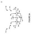
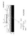
- semiconductor DRAM array 10includes a plurality of memory cells 12 each consisting of transistor 14 having gate 16 , body region 18 , which is electrically floating, source region 20 and drain region 22 .
- the body region 18is disposed between source region 20 and drain region 22 .
- body region 18is disposed on or above region 24 , which may be an insulation region (for example, in SOI material/substrate) or non-conductive region (for example, in bulk-type material/substrate).
- the insulation or non-conductive regionmay be disposed on substrate 26 .
- Datais written into or read from a selected memory cell by applying suitable control signals to a selected word line(s) 28 , a selected source line(s) 30 and/or a selected bit line(s) 32 .
- chargeis accumulated in or emitted and/or ejected from electrically floating body region 18 wherein the data states are defined by the amount of charge or carriers (for example, majority carriers) within electrically floating body region 18 .
- the entire contents of the Semiconductor Memory Device Patent Applicationincluding, for example, the features, attributes, architectures, configurations, materials, techniques and advantages described and illustrated therein, are incorporated by reference herein.
- memory cell 12 of DRAM array 10operates by accumulating in or emitting/ejecting majority carriers (electrons or holes) 34 from body region 18 of, for example, an N-channel transistor.
- majority carriersin this example, “holes”
- accumulating majority carriers (in this example, “holes”) 34 in body region 18 of memory cells 12 via, for example, impact ionization near source region 20 and/or drain region 22provides or results in a carrier concentration which is representative of a logic high or “1” data state. (See, FIG. 2A ).
- Emitting or ejecting majority carriers 30 from body region 18 via, for example, forward biasing the source/body junction and/or the drain/body junction,provides or results in a carrier concentration which is representative of a logic low or “0” data state. (See, FIG. 2B ).
- logic high or State “1”corresponds to an increased concentration of majority carries in the body region relative to an unprogrammed device and/or a device that is programmed with a logic low or State “0”.
- logic low or State “0”corresponds to a reduced concentration of majority carries in the body region relative to an unprogrammed device and/or a device that is programmed with a logic high or State “1”.
- a logic low(State “0”) by removing majority carriers from body region 18 through either source region 20 or drain region 22 of electrically floating body transistor 14 of memory cell 12 .
- majority carriersin this example, “holes” 34 in body region 18 of memory cells 12 are removed from memory cell 12 through drain region 22 .
- a current 36(electrons) flows from drain region 22 to source region 20 due to a channel forming in a portion of body region 18 immediately beneath the gate oxide when writing or programming a logic low (State “0”).
- writing or programming data into memory cells of an arraymay also “disturb” adjacent cell memory cells in memory device 10 .
- One technique to address the disturbance issueis to employ a two-cycle write or program technique.
- a logic low(State “0”) is written into all memory cells 12 connected to a word line 28 ; in the second cycle, a logic high (State “1”) is selectively written into memory cells 12 while an inhibit signal or voltage is applied to those memory cells 12 that are to remain at or maintain a logic low or State “0”.
- certain memory cells 12 connected to a given word linemay be written or programmed to a logic low (State “0”) using a first word line voltage; and certain other memory cells 12 , also connected to the given word line, may be written or programmed to a logic high (State “1”) using a second word line voltage.
- State “0”logic low
- State “1”logic high
- While electrically floating body transistors of memory cellsexhibit low leakage current characteristics, such memory cells often consume a considerable amount of power when programming a logic low (i.e., removing charge carriers from the body of the SOI device).
- many architectures and programming techniquestend to provide a two-cycle writing or programming techniques. This may reduce the speed or access time of the memory device, memory array, and/or memory cells.
- the present inventionsare directed to a semiconductor memory cell, array, architecture and device, and techniques for controlling and/or operating such cell and device; and more particularly, in one aspect, to a semiconductor dynamic random access memory (“DRAM”) cell, array, architecture and/or device wherein the memory cell includes an electrically floating body in which an electrical charge is stored.
- DRAMsemiconductor dynamic random access memory
- the present inventionsare directed to a semiconductor memory cell comprising an electrically floating body transistor including a source region, a drain region, a body region disposed between the source region and the drain region, wherein the body region is electrically floating; and a gate disposed over the body region and separated therefrom by a gate dielectric.
- the memory cellincludes a first data state which is representative of a first charge in the body region, and a second data state which is representative of a second charge in the body region wherein the second charge is substantially provided by removing charge from the body region through the gate.
- the first chargemay be comprised of an accumulation of majority carriers in the body region (for example, via impact ionization or band-to-band tunneling phenomenon).
- the second chargeis provided in the body region by applying (i) positive voltages to the drain region and source region, and (ii) a negative voltage to the gate. Indeed, in one embodiment, positive voltages are applied to the drain region and source region to substantially remove at least the first charge from the body region through the gate.
- the second chargein response to control signals applied to the gate, drain region and source region, is substantially provided in the body region by causing, forcing and/or inducing majority carriers in the floating body to tunnel through the gate dielectric to the gate.
- negative voltagesare applied to the drain region and source region and a positive voltage is applied to the gate to provide the second charge in the body region.
- the electrically floating body transistormay be a P-channel type transistor.
- the present inventionsare directed to a semiconductor memory cell array comprising a plurality of memory cells arranged in a matrix of rows and column.
- Each memory cell of the arrayincludes a transistor to constitute the memory cell.
- Each transistorcomprises a source region, a drain region, a body region disposed between the source region and the drain region, wherein the body region is electrically floating, and a gate disposed over the body region and separated therefrom by a gate dielectric.
- Each memory cell of the arrayincludes a first data state representative of a first charge in the body region of the associated transistor and a second data state representative of a second charge in the body region of the associated transistor wherein the second charge is substantially provided by removing charge from the body region through the gate of the associated transistor.
- the source region of the transistor of each memory cell corresponding to a first row of semiconductor dynamic random access memory cellsis connected to a first source line, and the gate of the transistor of each memory cell corresponding to the first row of semiconductor dynamic random access memory cells is connected to a first word line.
- the source region of the transistor of each memory cell corresponding to a second row of semiconductor dynamic random access memory cellsmay be connected to the first source line, and the gate of the transistor of each memory cell corresponding to the second row of semiconductor dynamic random access memory cells may be connected to a second word line.
- the source region of the transistor of each memory cell corresponding to a third row of semiconductor dynamic random access memory cellsmay be connected to a second source line, and wherein the gate of the transistor of each memory cell corresponding to the third row of semiconductor dynamic random access memory cells may be connected to a third word line.
- the drain region of the transistor of each memory cell corresponding to the first row of semiconductor dynamic random access memory cellsis the same region as the drain region of an adjacent memory cell of the third row.
- the first chargemay be comprised of an accumulation of majority carriers in the body region.
- a memory cell of the arraymay be programmed in the first data state via impact ionization or band-to-band tunneling phenomenon.
- a memory cell of the arraymay be programmed to the second data state by applying (i) a positive voltage to the drain region of the associated transistor, (ii) a positive voltage to the source region of the associated transistor, and (iii) a negative voltage to the gate of the associated transistor.
- the second chargeis substantially provided in the body region of the associated transistor by causing, forcing and/or inducing majority carriers in the floating body of the associated transistor to tunnel through the gate dielectric to the gate of the associated transistor.
- the memory cell of the arraymay be programmed to the second data state by applying (i) a negative voltage to the drain region of the associated transistor, (ii) a negative voltage to the source region of the associated transistor, and (iii) a positive voltage to the gate of the associated transistor.
- the present inventionsare directed to a method of programming a semiconductor memory cell comprising an electrically floating body transistor including a source region, a drain region, a body region disposed between the source region and the drain region, wherein the body region is electrically floating, and a gate disposed over the body region and separated therefrom by a gate dielectric.
- the memory cellincludes a first data state representative of a first charge in the body region and a second data state representative of a second charge in the body region wherein the second charge is substantially provided by removing charge from the body region through the gate.
- the methodcomprises applying a first voltage to the drain region applying a second voltage to the source region, applying a third voltage to the gate region wherein in response to the first, second and third voltages, the second charge is provided in the body region by causing, forcing and/or inducing majority carriers in the floating body to tunnel through the gate dielectric to the gate.
- first and second voltagesare positive, and the third voltage is negative. In another embodiment, the first and second voltages are negative, and the third voltage is positive.
- the methodmay further include providing the first data state in the memory cell via impact ionization or band-to-band tunneling phenomenon.
- FIG. 1Ais a schematic representation of a prior art semiconductor DRAM array including a plurality of memory cells comprised of one electrically floating body transistor;
- FIG. 1Bis a three dimensional view of an exemplary prior art memory cell comprised of one electrically floating body transistor (PD-SOI NMOS);
- PD-SOI NMOSelectrically floating body transistor
- FIG. 1Cis a cross-sectional view of the prior art memory cell of FIG. 1B , cross-sectioned along line C-C′;
- FIGS. 2A and 2Bare exemplary schematic illustrations of the charge relationship, for a given data state, of the floating body, source and drain regions of a prior art memory cell comprised of one electrically floating body transistor (PD-SOI NMOS);
- PD-SOI NMOSelectrically floating body transistor
- FIGS. 3A and 3Bare exemplary schematic illustrations of the charge relationship pertaining to conventional techniques for programming or writing a logic low or State “0” into an electrically floating body transistor (for example, a PD-SOI NMOS);
- FIG. 4Ais a schematic representation of a memory cell comprised of an electrically floating body transistor
- FIGS. 4B and 4Care exemplary schematic illustrations of the charge relationship, for programming or writing a logic low or State “0” into an electrically floating body transistor, according to one embodiment of the present invention
- FIGS. 5A and 5Care schematic illustrations of exemplary memory array architectures and memory arrays including, first and second memory cells (each having an electrically floating body transistor), wherein one of the memory cells is programmed to a logic low or State “0” in accordance with the technique of the present invention;
- FIG. 5Bis a schematic illustration of an exemplary memory array architecture and memory array (like the architecture and array of FIG. 5A ) including more than two memory cells and exemplary voltages for programming a logic low or State “0” in accordance with the technique of the present invention
- FIGS. 6A and 6Billustrate the GIDL mechanism for writing a logic high or State “1” into an electrically floating body transistor (for example, a PD-SOI NMOS);
- FIG. 7is an exemplary graphical illustration of selected control signals for writing State “1” and State “0” into a memory cell (having an electrically floating body transistor) wherein the memory cell is programmed to a logic low or State “0” in accordance with the technique of the present inventions and programmed to a logic high or State “1” using a technique that employs band-to-band tunneling phenomenon (described below as a “GIDL” technique);
- GIDLband-to-band tunneling phenomenon
- FIG. 8illustrates a memory cell including two electrically floating body transistors that are configured to have a common source region and connected gates, that may be controlled, programmed and/or operated according to one embodiment of the techniques of the present invention.
- FIGS. 9A and 9Billustrate the two data states of the memory cell having two electrically floating body transistors of, for example, FIG. 8 .
- the present inventionsare directed to a memory cell and/or technique of writing or programming a logic low or State “0” in a memory cell having an electrically floating body transistor.
- the present inventionsprogram a logic low or State “0” in the memory cell by causing, forcing and/or inducing majority carriers in the floating body to tunnel through or traverse the gate dielectric to the gate of the electrically floating body transistor (and, in many array configurations, the word line in the context of a memory cell array).
- a carrier concentrationwhich is representative of a logic low or “0” data state, is provided (or substantially provided) in the electrically floating body by removing majority carriers from the electrically floating body to the gate of the electrically floating body transistor.
- the memory cellmay be programmed to a logic low or State “0” while the electrically floating body transistor is in the “OFF” state or substantially “OFF” state (for example, when the device has no (or practically no) channel and/or channel current between the source and drain).
- the memory cellmay be programmed whereby there is little to no current/power consumption by the electrically floating body transistor and/or from memory array having a plurality of electrically floating body transistors.
- the present inventionsinclude memory cell 12 having electrically floating body transistor 14 .
- electrically floating body transistor 14is a N-channel type transistor. As such, majority carriers 34 are “holes”.
- electrically floating body transistor 14is programmed in a logic low or State “0” by causing, forcing and/or inducing majority carriers in floating body 18 of electrically floating body transistor 14 to tunnel through or traverse gate dielectric 38 to gate 16 of transistor 14 .
- the “holes”may be forced and/or induced to tunnel to gate 16 by applying a sufficiently large negative voltage to gate 16 relative to source 20 and drain 22 .
- 0 voltsmay be applied to source region 20 and drain region 22 and a negative voltage (for example, ⁇ 2 volts) may be applied to gate 16 to cause, force and/or induce the holes to tunnel through gate dielectric 38 to gate 16 .
- electrically floating body transistor 14is a P-channel type transistor.
- majority carriers 34are “electrons”.
- electrically floating body transistor 14is programmed in a logic low or State “0” by causing, forcing and/or inducing majority carriers 34 in floating body 18 to tunnel through or traverse gate dielectric 38 to gate 16 of transistor 14 .
- the electron majority carriersmay be forced and/or induced to tunnel to gate 16 by applying a sufficiently large positive voltage to gate 16 relative to source 20 and drain 22 .
- 0 voltsmay be applied to source region 20 and drain region 22 and a positive voltage (for example, +2 volts) may be applied to gate 16 to cause, force and/or induce the holes to tunnel through gate dielectric 38 to gate 16 .
- a positive voltagefor example, +2 volts
- the present inventionsmay be implemented using any technique or operation to write or store a logic high or State “1” in the electrically floating body transistor of the memory cell.
- impact ionization or band-to-band tunneling phenomenondiscussed in detail below
- any technique, whether now known or later developed,may be employed to write or store a logic high or State “1” in the electrically floating body transistor of the memory cell.
- the present inventionis a memory array, having a plurality of memory cells each including an electrically floating body transistor, and/or technique of writing or programming data into one or more memory cells of such a memory array.
- the data states of adjacent memory cells and/or memory cells that share a word linemay be individually programmed via a one step write.
- memory array 10may include first memory cell 12 a , having electrically floating body transistor 14 a , and second memory cell 12 b , having electrically floating body transistor 14 b .
- the word line 28is connected to gates 16 a and 16 b of electrically floating body transistors 14 a and 14 b , respectively, to program the data state of memory cells 12 a and 12 b.
- memory cells 12 a and 12 bmay be individually programmed via a one step write technique.
- memory cell 12 amay be programmed to logic low or State “0”, as mentioned above, by causing, forcing and/or inducing majority carriers 34 in floating body 18 a to tunnel through gate dielectric to gate 16 a of transistor 14 a .
- the memory cell 12 bmay be programmed to a logic high or State “1” using, for example, a technique that employs band-to-band tunneling phenomenon (hereinafter “gate induced drain leakage” (i.e., “GIDL”) or “gate induced source leakage” (i.e., GISL), as the case may be).
- GIDLband-to-band tunneling phenomenon
- GISLgate induced source leakage
- transistor 14a logic high or State “1” may be stored in transistor 14 by creating excess majority carriers in electrically floating body 18 of transistor 14 .
- the majority carriers 34(“holes” in this embodiment where transistor 14 is an N-channel type transistor) may be created by a tunneling mechanism that appears in the silicon at the edge of drain region 22 . That is, where a negative voltage is applied on gate 16 and a positive voltage is applied at drain region 22 , this voltage difference may create a silicon band bending that then leads to a valence band electron tunneling into the conduction band. (See, FIGS. 6A and 6B ).
- the GIDL effect or mechanismmay be a very efficient manner of writing or storing a logic high (State “1”) because it tends not to cause a channel to form in electrically floating body 18 of transistor 14 and, as such, little to no channel current flows between source region 20 and drain region 18 .
- the GIDL technique of writing or storing a logic highmay reduce the current consumption relative to the impact ionization technique.
- electrically floating body transistor 14 amay be programmed to a logic low or State “0” by applying 0 volts to source region 20 a and drain region 22 a and a negative voltage (for example, ⁇ 2 volts) to gate 16 . In this way, majority carriers tunnel through gate dielectric to gate 16 a of transistor 14 a .
- memory cell 12 bmay be programmed to a logic high or State “1” by applying a sufficient positive voltage (for example, 1.8 volts) to drain region 22 b (i.e., a GIDL programming technique).
- transistors 14 a and 14 b“share” or include a common source region and, as such, 0 volts is also applied to source region 20 b .
- gates 16 a and 16 b of transistors 14 a and 14 bare connected to the same word line 28 and, as such, a negative voltage (for example, ⁇ 2 volts) is also applied to gate 16 b .
- a negative voltagefor example, ⁇ 2 volts
- FIG. 7is an exemplary graphical illustration of selected control signals for writing State “1” and State “0” into memory cells 12 a and 12 b of FIG. 5A and memory cells 12 a 1 and 12 a 2 of FIG. 5B .
- a logic high or State “1”may be stored in a memory cell by a tunneling mechanism that appears in the silicon at the edge of the source under specific conditions (referred to above as “gate induced source leakage” or “GISL”).
- GISLgate induced source leakage
- GISL effect or mechanismmay be a very efficient manner of writing or storing a logic high (State “1”) because, like GIDL, GISL tends not to cause a channel to form in the body and, as such, little to no channel current flows between the source and the drain.
- the memory arraysmay be comprised of N-channel, P-channel and/or both types of transistors.
- circuitry that is peripheral to the memory arrayfor example, sense amplifiers or comparators, row and column address decoders, as well as line drivers (not illustrated herein) may include P-channel and/or N-channel type transistors.
- P-channel type transistorsare employed as memory cells 12 in the memory array(s)
- suitable write and read voltagesfor example, negative voltages
- the electrically floating body transistorwhich is programmed to a logic low or State “0” according to the techniques of the present inventions, may be employed in any electrically floating body memory cell, and/or architecture, layout, structure and/or configuration employing such electrically floating body memory cells.
- an electrically floating body transistorwhich is programmed to a logic low or State “0” according to the techniques of the present inventions, may be implemented in the memory cell, architecture, layout, structure and/or configuration described and illustrated in the following provisional and non-provisional U.S. patent applications:
- the memory cellsmay be controlled (for example, programmed or read) using any of the control circuitry described and illustrated in the above-referenced U.S. patent applications. For the sake of brevity, those discussions will not be repeated; such control circuitry is incorporated herein by reference. Indeed, all such control/selection techniques and circuitry therefor, whether now known or later developed, are intended to fall within the scope of the present inventions.
- the data stored in (or write the data into) memory cells 12 of DRAM array/device 10may be read using many well known circuitry and techniques, including those described in the above-referenced U.S. patent applications.
- the present inventionsmay also employ the read circuitry and techniques described and illustrated in U.S. patent application Ser. No. 10/840,902, which was filed by Portmann et al. on May 7, 2004, and entitled “Reference Current Generator, and Method of Programming, Adjusting and/or Operating Same”.
- the present inventionsmay employ the read operation techniques described and illustrated in U.S. Provisional Patent Application Ser. No. 60/718,417, which was filed by Bauser on Sep. 19, 2005, and entitled “Method and Circuitry to Generate a Reference Current for Reading a Memory Cell Having an Electrically Floating Body Transistor, and Device Implementing Same”.
- the entire contents of the U.S. Provisional Patent Application Ser. No. 60/718,417are incorporated herein by reference.
- a sense amplifier(not illustrated) may be employed to read the data stored in memory cells 12 .
- the sense amplifiermay sense the data state stored in memory cell 12 using voltage or current sensing techniques.
- the current sense amplifiermay compare the cell current to a reference current, for example, the current of a reference cell (not illustrated). From that comparison, it may be determined whether memory cell 12 contained a logic high (relatively more majority carries 34 contained within body region 18 ) or logic low data state (relatively less majority carries 28 contained within body region 18 ).
- a logic highrelatively more majority carries 34 contained within body region 18
- logic low data state(relatively less majority carries 28 contained within body region 18 ).
- each memory cell 12 in the exemplary embodimentsincludes one transistor 14
- memory cell 12may include two transistors, as described and illustrated in application Ser. No. 10/829,877, which was filed by Ferrant et al. on Apr. 22, 2004 and entitled “Semiconductor Memory Cell, Array, Architecture and Device, and Method of Operating Same”.
- two-transistor memory cell 12includes transistors 14 a and 14 b which store complementary data states.
- transistors 14 a and 14 b of memory cell 12include a layout whereby transistors 14 a and 14 b include (1) common source regions 20 a and 20 b , respectively, and (2) gates 16 a and 16 b , respectively, which are connected to the same word line 28 .
- two-transistor memory cell 12includes first transistor 14 a that maintains a complementary state relative to second transistor 14 b .
- first transistor 14 athat maintains a complementary state relative to second transistor 14 b .
- one of the transistors of the memory cellstores a logic low (a binary “0”) and the other transistor of the memory cell stores a logic high (a binary “1”).
- the transistor 14 that is programmed to a logic low or State “0”may be programmed according to the techniques of the present inventions. Indeed, the transistors 14 a or 14 b of FIGS. 9A and 9B may be programmed using GIDL or GISL technique for writing or programming a logic high or State “1”.
- any of the architectures, layouts, structures and/or configurations, as well as the programming and reading operations described and illustrated in application Ser. No. 10/829,877, which was filed by Ferrant et al. on Apr. 22, 2004 and entitled “Semiconductor Memory Cell, Array, Architecture and Device, and Method of Operating Same”may be employed in conjunction with the inventions described and illustrated herein.
- those discussionswill not be repeated; rather, they are incorporated by reference herein.
- the electrically floating memory cells, transistors and/or memory array(s)may be fabricated using well known techniques and/or materials. Indeed, any fabrication technique and/or material, whether now known or later developed, may be employed to fabricate the electrically floating memory cells, transistors and/or memory array(s).
- the present inventionsmay employ silicon (whether bulk-type or SOI, as described above), germanium, silicon/germanium, and gallium arsenide or any other semiconductor material in which transistors may be formed.
- the electrically floating memory cells, transistors and/or memory array(s)may employ the techniques described and illustrated in non-provisional patent application entitled “Integrated Circuit Device, and Method of Fabricating Same”, which was filed on Jul. 2, 2004, by Fazan, and assigned Ser. No.
- Integrated Circuit Device Patent Application10/884,481 (hereinafter “Integrated Circuit Device Patent Application”).
- Integrated Circuit Device Patent ApplicationThe entire contents of the Integrated Circuit Device Patent Application, including, for example, the inventions, features, attributes, architectures, configurations, materials, techniques and advantages described and illustrated therein, are hereby incorporated by reference herein.
- memory array 10may be integrated with SOI logic transistors, as described and illustrated in the Integrated Circuit Device Patent Application.
- an integrated circuit deviceincludes memory section (having, for example, PD or FD SOI memory transistors 14 ) and logic section having, for example, high performance transistors, such as Fin-FET, multiple gate transistors, and/or non-high performance transistors (for example, single gate transistors that do not possess the performance characteristics of high performance transistors—not illustrated).
- high performance transistorssuch as Fin-FET
- multiple gate transistorsmultiple gate transistors
- non-high performance transistorsfor example, single gate transistors that do not possess the performance characteristics of high performance transistors—not illustrated.
- the memory arraysmay be comprised of N-channel, P-channel and/or both types of transistors, as well as partially depleted and/or fully depleted type transistors.
- circuitry that is peripheral to the memory arraymay include fully depleted type transistors (whether P-channel and/or N-channel type).
- circuitrymay include partially depleted type transistors (whether P-channel and/or N-channel type).
- electrically floating body transistor 14may be a symmetrical or non-symmetrical device. Where transistor 14 is symmetrical, the source and drain regions are essentially interchangeable. However, where transistor 14 is a non-symmetrical device, the source or drain regions of transistor 14 have different electrical, physical, doping concentration and/or doping profile characteristics. As such, the source or drain regions of a non-symmetrical device are typically not interchangeable. This notwithstanding, the drain region of the electrically floating N-channel type transistor of the memory cell (whether the source and drain regions are interchangeable or not) is that region of the transistor that is connected to the bit line/sense amplifier.
- the illustrated voltage levels to implement the write and read operationsare exemplary.
- the indicated voltage levelsmay be relative or absolute. That is, for example, a logic low may be written into transistor 12 a (see, for example, FIG. 5B ) using the voltages indicated therein.
- the voltages indicatedmay be relative in that each voltage level, for example, may be increased or decreased by a given voltage amount (for example, each voltage may be increased by 0.25 or 0.5 volts) whether one or more of the voltages (for example, the source, drain or gate voltages) become or are positive and negative.
- each of the aspects of the present inventions, and/or embodiments thereofmay be employed alone or in combination with one or more of such aspects and/or embodiments.
- those permutations and combinationswill not be discussed separately herein.
- the present inventionsare neither limited to any single aspect (nor embodiment thereof), nor to any combinations and/or permutations of such aspects and/or embodiments.
Landscapes
- Engineering & Computer Science (AREA)
- Microelectronics & Electronic Packaging (AREA)
- Computer Hardware Design (AREA)
- Semiconductor Memories (AREA)
- Non-Volatile Memory (AREA)
Abstract
Description
Claims (26)
Priority Applications (1)
| Application Number | Priority Date | Filing Date | Title |
|---|---|---|---|
| US11/247,727US7476939B2 (en) | 2004-11-04 | 2005-10-11 | Memory cell having an electrically floating body transistor and programming technique therefor |
Applications Claiming Priority (2)
| Application Number | Priority Date | Filing Date | Title |
|---|---|---|---|
| US62524804P | 2004-11-04 | 2004-11-04 | |
| US11/247,727US7476939B2 (en) | 2004-11-04 | 2005-10-11 | Memory cell having an electrically floating body transistor and programming technique therefor |
Publications (2)
| Publication Number | Publication Date |
|---|---|
| US20060091462A1 US20060091462A1 (en) | 2006-05-04 |
| US7476939B2true US7476939B2 (en) | 2009-01-13 |
Family
ID=36260827
Family Applications (1)
| Application Number | Title | Priority Date | Filing Date |
|---|---|---|---|
| US11/247,727Active2025-11-05US7476939B2 (en) | 2004-11-04 | 2005-10-11 | Memory cell having an electrically floating body transistor and programming technique therefor |
Country Status (1)
| Country | Link |
|---|---|
| US (1) | US7476939B2 (en) |
Cited By (236)
| Publication number | Priority date | Publication date | Assignee | Title |
|---|---|---|---|---|
| US20080285357A1 (en)* | 2006-07-21 | 2008-11-20 | Hee Bok Kang | 1-transistor type dram cell, dram device and dram comprising thereof and driving method thereof and manufacturing method thereof |
| US20100020597A1 (en)* | 2005-09-07 | 2010-01-28 | Serguei Okhonin | Memory Cell and Memory Cell Array Having an Electrically Floating Body Transistor, and Methods of Operating Same |
| US20110031997A1 (en)* | 2009-04-14 | 2011-02-10 | NuPGA Corporation | Method for fabrication of a semiconductor device and structure |
| US20110084314A1 (en)* | 2009-10-12 | 2011-04-14 | NuPGA Corporation | System comprising a semiconductor device and structure |
| US20110092030A1 (en)* | 2009-04-14 | 2011-04-21 | NuPGA Corporation | System comprising a semiconductor device and structure |
| US20110108888A1 (en)* | 2009-04-14 | 2011-05-12 | NuPGA Corporation | System comprising a semiconductor device and structure |
| US20110121366A1 (en)* | 2009-04-14 | 2011-05-26 | NuPGA Corporation | System comprising a semiconductor device and structure |
| US20110215396A1 (en)* | 2010-03-02 | 2011-09-08 | Micron Technology, Inc. | Semiconductor cells, arrays, devices and systems having a buried conductive line and methods for forming the same |
| US20110215371A1 (en)* | 2010-03-02 | 2011-09-08 | Micron Technology, Inc. | Thyristor based memory cells, devices and systems including the same and methods for forming the same |
| US20110215408A1 (en)* | 2010-03-02 | 2011-09-08 | Micron Technology, Inc. | Floating body cell structures, devices including same, and methods for forming same |
| US8134867B2 (en)* | 2006-04-07 | 2012-03-13 | Micron Technology, Inc. | Memory array having a programmable word length, and method of operating same |
| US8163581B1 (en) | 2010-10-13 | 2012-04-24 | Monolith IC 3D | Semiconductor and optoelectronic devices |
| US8203148B2 (en) | 2010-10-11 | 2012-06-19 | Monolithic 3D Inc. | Semiconductor device and structure |
| US8258810B2 (en) | 2010-09-30 | 2012-09-04 | Monolithic 3D Inc. | 3D semiconductor device |
| US8273610B2 (en) | 2010-11-18 | 2012-09-25 | Monolithic 3D Inc. | Method of constructing a semiconductor device and structure |
| US8283215B2 (en) | 2010-10-13 | 2012-10-09 | Monolithic 3D Inc. | Semiconductor and optoelectronic devices |
| US8294159B2 (en) | 2009-10-12 | 2012-10-23 | Monolithic 3D Inc. | Method for fabrication of a semiconductor device and structure |
| US8298875B1 (en) | 2011-03-06 | 2012-10-30 | Monolithic 3D Inc. | Method for fabrication of a semiconductor device and structure |
| US8362800B2 (en) | 2010-10-13 | 2013-01-29 | Monolithic 3D Inc. | 3D semiconductor device including field repairable logics |
| US8373230B1 (en) | 2010-10-13 | 2013-02-12 | Monolithic 3D Inc. | Method for fabrication of a semiconductor device and structure |
| US8373439B2 (en) | 2009-04-14 | 2013-02-12 | Monolithic 3D Inc. | 3D semiconductor device |
| US8379458B1 (en) | 2010-10-13 | 2013-02-19 | Monolithic 3D Inc. | Semiconductor device and structure |
| US8378494B2 (en) | 2009-04-14 | 2013-02-19 | Monolithic 3D Inc. | Method for fabrication of a semiconductor device and structure |
| US8378715B2 (en) | 2009-04-14 | 2013-02-19 | Monolithic 3D Inc. | Method to construct systems |
| US8384426B2 (en) | 2009-04-14 | 2013-02-26 | Monolithic 3D Inc. | Semiconductor device and structure |
| US8405420B2 (en) | 2009-04-14 | 2013-03-26 | Monolithic 3D Inc. | System comprising a semiconductor device and structure |
| US8427200B2 (en) | 2009-04-14 | 2013-04-23 | Monolithic 3D Inc. | 3D semiconductor device |
| US8440542B2 (en) | 2010-10-11 | 2013-05-14 | Monolithic 3D Inc. | Semiconductor device and structure |
| US8450804B2 (en) | 2011-03-06 | 2013-05-28 | Monolithic 3D Inc. | Semiconductor device and structure for heat removal |
| US8461035B1 (en) | 2010-09-30 | 2013-06-11 | Monolithic 3D Inc. | Method for fabrication of a semiconductor device and structure |
| US8476145B2 (en) | 2010-10-13 | 2013-07-02 | Monolithic 3D Inc. | Method of fabricating a semiconductor device and structure |
| US8492886B2 (en) | 2010-02-16 | 2013-07-23 | Monolithic 3D Inc | 3D integrated circuit with logic |
| US8536023B2 (en) | 2010-11-22 | 2013-09-17 | Monolithic 3D Inc. | Method of manufacturing a semiconductor device and structure |
| US8541819B1 (en) | 2010-12-09 | 2013-09-24 | Monolithic 3D Inc. | Semiconductor device and structure |
| US8557632B1 (en) | 2012-04-09 | 2013-10-15 | Monolithic 3D Inc. | Method for fabrication of a semiconductor device and structure |
| US8574929B1 (en) | 2012-11-16 | 2013-11-05 | Monolithic 3D Inc. | Method to form a 3D semiconductor device and structure |
| US8581349B1 (en) | 2011-05-02 | 2013-11-12 | Monolithic 3D Inc. | 3D memory semiconductor device and structure |
| US8598621B2 (en) | 2011-02-11 | 2013-12-03 | Micron Technology, Inc. | Memory cells, memory arrays, methods of forming memory cells, and methods of forming a shared doped semiconductor region of a vertically oriented thyristor and a vertically oriented access transistor |
| US8642416B2 (en) | 2010-07-30 | 2014-02-04 | Monolithic 3D Inc. | Method of forming three dimensional integrated circuit devices using layer transfer technique |
| US8669778B1 (en) | 2009-04-14 | 2014-03-11 | Monolithic 3D Inc. | Method for design and manufacturing of a 3D semiconductor device |
| US8674470B1 (en) | 2012-12-22 | 2014-03-18 | Monolithic 3D Inc. | Semiconductor device and structure |
| US8686428B1 (en) | 2012-11-16 | 2014-04-01 | Monolithic 3D Inc. | Semiconductor device and structure |
| US8687399B2 (en) | 2011-10-02 | 2014-04-01 | Monolithic 3D Inc. | Semiconductor device and structure |
| US8709880B2 (en) | 2010-07-30 | 2014-04-29 | Monolithic 3D Inc | Method for fabrication of a semiconductor device and structure |
| US8742476B1 (en) | 2012-11-27 | 2014-06-03 | Monolithic 3D Inc. | Semiconductor device and structure |
| US8803206B1 (en) | 2012-12-29 | 2014-08-12 | Monolithic 3D Inc. | 3D semiconductor device and structure |
| US8902663B1 (en) | 2013-03-11 | 2014-12-02 | Monolithic 3D Inc. | Method of maintaining a memory state |
| US8901613B2 (en) | 2011-03-06 | 2014-12-02 | Monolithic 3D Inc. | Semiconductor device and structure for heat removal |
| US8975670B2 (en) | 2011-03-06 | 2015-03-10 | Monolithic 3D Inc. | Semiconductor device and structure for heat removal |
| US8994404B1 (en) | 2013-03-12 | 2015-03-31 | Monolithic 3D Inc. | Semiconductor device and structure |
| US9000557B2 (en) | 2012-03-17 | 2015-04-07 | Zvi Or-Bach | Semiconductor device and structure |
| US9029173B2 (en) | 2011-10-18 | 2015-05-12 | Monolithic 3D Inc. | Method for fabrication of a semiconductor device and structure |
| US9099424B1 (en) | 2012-08-10 | 2015-08-04 | Monolithic 3D Inc. | Semiconductor system, device and structure with heat removal |
| US9099526B2 (en) | 2010-02-16 | 2015-08-04 | Monolithic 3D Inc. | Integrated circuit device and structure |
| US9117749B1 (en) | 2013-03-15 | 2015-08-25 | Monolithic 3D Inc. | Semiconductor device and structure |
| US9197804B1 (en) | 2011-10-14 | 2015-11-24 | Monolithic 3D Inc. | Semiconductor and optoelectronic devices |
| US9219005B2 (en) | 2011-06-28 | 2015-12-22 | Monolithic 3D Inc. | Semiconductor system and device |
| US9269795B2 (en) | 2011-07-26 | 2016-02-23 | Micron Technology, Inc. | Circuit structures, memory circuitry, and methods |
| US9361966B2 (en) | 2011-03-08 | 2016-06-07 | Micron Technology, Inc. | Thyristors |
| US9509313B2 (en) | 2009-04-14 | 2016-11-29 | Monolithic 3D Inc. | 3D semiconductor device |
| US9508854B2 (en) | 2013-12-06 | 2016-11-29 | Ecole Polytechnique Federale De Lausanne (Epfl) | Single field effect transistor capacitor-less memory device and method of operating the same |
| TWI566243B (en)* | 2010-02-07 | 2017-01-11 | 季諾半導體股份有限公司 | Semiconductor memory elements - floating body transistors with conduction, semiconductor memory elements - non-permanent and permanent functions and methods of operation |
| US9577642B2 (en) | 2009-04-14 | 2017-02-21 | Monolithic 3D Inc. | Method to form a 3D semiconductor device |
| US9608119B2 (en) | 2010-03-02 | 2017-03-28 | Micron Technology, Inc. | Semiconductor-metal-on-insulator structures, methods of forming such structures, and semiconductor devices including such structures |
| US9646869B2 (en) | 2010-03-02 | 2017-05-09 | Micron Technology, Inc. | Semiconductor devices including a diode structure over a conductive strap and methods of forming such semiconductor devices |
| US9871034B1 (en) | 2012-12-29 | 2018-01-16 | Monolithic 3D Inc. | Semiconductor device and structure |
| US9953925B2 (en) | 2011-06-28 | 2018-04-24 | Monolithic 3D Inc. | Semiconductor system and device |
| US10043781B2 (en) | 2009-10-12 | 2018-08-07 | Monolithic 3D Inc. | 3D semiconductor device and structure |
| US10115663B2 (en) | 2012-12-29 | 2018-10-30 | Monolithic 3D Inc. | 3D semiconductor device and structure |
| US10127344B2 (en) | 2013-04-15 | 2018-11-13 | Monolithic 3D Inc. | Automation for monolithic 3D devices |
| US10157909B2 (en) | 2009-10-12 | 2018-12-18 | Monolithic 3D Inc. | 3D semiconductor device and structure |
| US10217667B2 (en) | 2011-06-28 | 2019-02-26 | Monolithic 3D Inc. | 3D semiconductor device, fabrication method and system |
| US10224279B2 (en) | 2013-03-15 | 2019-03-05 | Monolithic 3D Inc. | Semiconductor device and structure |
| US10290682B2 (en) | 2010-10-11 | 2019-05-14 | Monolithic 3D Inc. | 3D IC semiconductor device and structure with stacked memory |
| US10297586B2 (en) | 2015-03-09 | 2019-05-21 | Monolithic 3D Inc. | Methods for processing a 3D semiconductor device |
| US10325651B2 (en) | 2013-03-11 | 2019-06-18 | Monolithic 3D Inc. | 3D semiconductor device with stacked memory |
| US10354995B2 (en) | 2009-10-12 | 2019-07-16 | Monolithic 3D Inc. | Semiconductor memory device and structure |
| US10366970B2 (en) | 2009-10-12 | 2019-07-30 | Monolithic 3D Inc. | 3D semiconductor device and structure |
| US10373956B2 (en) | 2011-03-01 | 2019-08-06 | Micron Technology, Inc. | Gated bipolar junction transistors, memory arrays, and methods of forming gated bipolar junction transistors |
| US10381328B2 (en) | 2015-04-19 | 2019-08-13 | Monolithic 3D Inc. | Semiconductor device and structure |
| US10388568B2 (en) | 2011-06-28 | 2019-08-20 | Monolithic 3D Inc. | 3D semiconductor device and system |
| US10388863B2 (en) | 2009-10-12 | 2019-08-20 | Monolithic 3D Inc. | 3D memory device and structure |
| US10418369B2 (en) | 2015-10-24 | 2019-09-17 | Monolithic 3D Inc. | Multi-level semiconductor memory device and structure |
| US10497713B2 (en) | 2010-11-18 | 2019-12-03 | Monolithic 3D Inc. | 3D semiconductor memory device and structure |
| US10515981B2 (en) | 2015-09-21 | 2019-12-24 | Monolithic 3D Inc. | Multilevel semiconductor device and structure with memory |
| US10522225B1 (en) | 2015-10-02 | 2019-12-31 | Monolithic 3D Inc. | Semiconductor device with non-volatile memory |
| US10600888B2 (en) | 2012-04-09 | 2020-03-24 | Monolithic 3D Inc. | 3D semiconductor device |
| US10600657B2 (en) | 2012-12-29 | 2020-03-24 | Monolithic 3D Inc | 3D semiconductor device and structure |
| US10651054B2 (en) | 2012-12-29 | 2020-05-12 | Monolithic 3D Inc. | 3D semiconductor device and structure |
| US10679977B2 (en) | 2010-10-13 | 2020-06-09 | Monolithic 3D Inc. | 3D microdisplay device and structure |
| US10825779B2 (en) | 2015-04-19 | 2020-11-03 | Monolithic 3D Inc. | 3D semiconductor device and structure |
| US10833108B2 (en) | 2010-10-13 | 2020-11-10 | Monolithic 3D Inc. | 3D microdisplay device and structure |
| US10840239B2 (en) | 2014-08-26 | 2020-11-17 | Monolithic 3D Inc. | 3D semiconductor device and structure |
| US10847540B2 (en) | 2015-10-24 | 2020-11-24 | Monolithic 3D Inc. | 3D semiconductor memory device and structure |
| US10892016B1 (en) | 2019-04-08 | 2021-01-12 | Monolithic 3D Inc. | 3D memory semiconductor devices and structures |
| US10892169B2 (en) | 2012-12-29 | 2021-01-12 | Monolithic 3D Inc. | 3D semiconductor device and structure |
| US10896931B1 (en) | 2010-10-11 | 2021-01-19 | Monolithic 3D Inc. | 3D semiconductor device and structure |
| US10903089B1 (en) | 2012-12-29 | 2021-01-26 | Monolithic 3D Inc. | 3D semiconductor device and structure |
| US10910364B2 (en) | 2009-10-12 | 2021-02-02 | Monolitaic 3D Inc. | 3D semiconductor device |
| US10943934B2 (en) | 2010-10-13 | 2021-03-09 | Monolithic 3D Inc. | Multilevel semiconductor device and structure |
| US10978501B1 (en) | 2010-10-13 | 2021-04-13 | Monolithic 3D Inc. | Multilevel semiconductor device and structure with waveguides |
| US10998374B1 (en) | 2010-10-13 | 2021-05-04 | Monolithic 3D Inc. | Multilevel semiconductor device and structure |
| US11004694B1 (en) | 2012-12-29 | 2021-05-11 | Monolithic 3D Inc. | 3D semiconductor device and structure |
| US11004719B1 (en) | 2010-11-18 | 2021-05-11 | Monolithic 3D Inc. | Methods for producing a 3D semiconductor memory device and structure |
| US11011507B1 (en) | 2015-04-19 | 2021-05-18 | Monolithic 3D Inc. | 3D semiconductor device and structure |
| US11018191B1 (en) | 2010-10-11 | 2021-05-25 | Monolithic 3D Inc. | 3D semiconductor device and structure |
| US11018156B2 (en) | 2019-04-08 | 2021-05-25 | Monolithic 3D Inc. | 3D memory semiconductor devices and structures |
| US11018133B2 (en) | 2009-10-12 | 2021-05-25 | Monolithic 3D Inc. | 3D integrated circuit |
| US11018116B2 (en) | 2012-12-22 | 2021-05-25 | Monolithic 3D Inc. | Method to form a 3D semiconductor device and structure |
| US11018042B1 (en) | 2010-11-18 | 2021-05-25 | Monolithic 3D Inc. | 3D semiconductor memory device and structure |
| US11024673B1 (en) | 2010-10-11 | 2021-06-01 | Monolithic 3D Inc. | 3D semiconductor device and structure |
| US11030371B2 (en) | 2013-04-15 | 2021-06-08 | Monolithic 3D Inc. | Automation for monolithic 3D devices |
| US11031394B1 (en) | 2014-01-28 | 2021-06-08 | Monolithic 3D Inc. | 3D semiconductor device and structure |
| US11031275B2 (en) | 2010-11-18 | 2021-06-08 | Monolithic 3D Inc. | 3D semiconductor device and structure with memory |
| US11043523B1 (en) | 2010-10-13 | 2021-06-22 | Monolithic 3D Inc. | Multilevel semiconductor device and structure with image sensors |
| US11056468B1 (en) | 2015-04-19 | 2021-07-06 | Monolithic 3D Inc. | 3D semiconductor device and structure |
| US11063024B1 (en) | 2012-12-22 | 2021-07-13 | Monlithic 3D Inc. | Method to form a 3D semiconductor device and structure |
| US11063071B1 (en) | 2010-10-13 | 2021-07-13 | Monolithic 3D Inc. | Multilevel semiconductor device and structure with waveguides |
| US11088130B2 (en) | 2014-01-28 | 2021-08-10 | Monolithic 3D Inc. | 3D semiconductor device and structure |
| US11087995B1 (en) | 2012-12-29 | 2021-08-10 | Monolithic 3D Inc. | 3D semiconductor device and structure |
| US11088050B2 (en) | 2012-04-09 | 2021-08-10 | Monolithic 3D Inc. | 3D semiconductor device with isolation layers |
| US11094576B1 (en) | 2010-11-18 | 2021-08-17 | Monolithic 3D Inc. | Methods for producing a 3D semiconductor memory device and structure |
| US11107808B1 (en) | 2014-01-28 | 2021-08-31 | Monolithic 3D Inc. | 3D semiconductor device and structure |
| US11107721B2 (en) | 2010-11-18 | 2021-08-31 | Monolithic 3D Inc. | 3D semiconductor device and structure with NAND logic |
| US11114464B2 (en) | 2015-10-24 | 2021-09-07 | Monolithic 3D Inc. | 3D semiconductor device and structure |
| US11114427B2 (en) | 2015-11-07 | 2021-09-07 | Monolithic 3D Inc. | 3D semiconductor processor and memory device and structure |
| US11121021B2 (en) | 2010-11-18 | 2021-09-14 | Monolithic 3D Inc. | 3D semiconductor device and structure |
| US11133344B2 (en) | 2010-10-13 | 2021-09-28 | Monolithic 3D Inc. | Multilevel semiconductor device and structure with image sensors |
| US11158652B1 (en) | 2019-04-08 | 2021-10-26 | Monolithic 3D Inc. | 3D memory semiconductor devices and structures |
| US11158674B2 (en) | 2010-10-11 | 2021-10-26 | Monolithic 3D Inc. | Method to produce a 3D semiconductor device and structure |
| US11164898B2 (en) | 2010-10-13 | 2021-11-02 | Monolithic 3D Inc. | Multilevel semiconductor device and structure |
| US11164770B1 (en) | 2010-11-18 | 2021-11-02 | Monolithic 3D Inc. | Method for producing a 3D semiconductor memory device and structure |
| US11164811B2 (en) | 2012-04-09 | 2021-11-02 | Monolithic 3D Inc. | 3D semiconductor device with isolation layers and oxide-to-oxide bonding |
| US11163112B2 (en) | 2010-10-13 | 2021-11-02 | Monolithic 3D Inc. | Multilevel semiconductor device and structure with electromagnetic modulators |
| US11177140B2 (en) | 2012-12-29 | 2021-11-16 | Monolithic 3D Inc. | 3D semiconductor device and structure |
| US11211279B2 (en) | 2010-11-18 | 2021-12-28 | Monolithic 3D Inc. | Method for processing a 3D integrated circuit and structure |
| US11217565B2 (en) | 2012-12-22 | 2022-01-04 | Monolithic 3D Inc. | Method to form a 3D semiconductor device and structure |
| US11227897B2 (en) | 2010-10-11 | 2022-01-18 | Monolithic 3D Inc. | Method for producing a 3D semiconductor memory device and structure |
| US11251149B2 (en) | 2016-10-10 | 2022-02-15 | Monolithic 3D Inc. | 3D memory device and structure |
| US11257867B1 (en) | 2010-10-11 | 2022-02-22 | Monolithic 3D Inc. | 3D semiconductor device and structure with oxide bonds |
| US11270055B1 (en) | 2013-04-15 | 2022-03-08 | Monolithic 3D Inc. | Automation for monolithic 3D devices |
| US11296115B1 (en) | 2015-10-24 | 2022-04-05 | Monolithic 3D Inc. | 3D semiconductor device and structure |
| US11296106B2 (en) | 2019-04-08 | 2022-04-05 | Monolithic 3D Inc. | 3D memory semiconductor devices and structures |
| US11309292B2 (en) | 2012-12-22 | 2022-04-19 | Monolithic 3D Inc. | 3D semiconductor device and structure with metal layers |
| US11315980B1 (en) | 2010-10-11 | 2022-04-26 | Monolithic 3D Inc. | 3D semiconductor device and structure with transistors |
| US11327227B2 (en) | 2010-10-13 | 2022-05-10 | Monolithic 3D Inc. | Multilevel semiconductor device and structure with electromagnetic modulators |
| US11329059B1 (en) | 2016-10-10 | 2022-05-10 | Monolithic 3D Inc. | 3D memory devices and structures with thinned single crystal substrates |
| US11341309B1 (en) | 2013-04-15 | 2022-05-24 | Monolithic 3D Inc. | Automation for monolithic 3D devices |
| US11355380B2 (en) | 2010-11-18 | 2022-06-07 | Monolithic 3D Inc. | Methods for producing 3D semiconductor memory device and structure utilizing alignment marks |
| US11355381B2 (en) | 2010-11-18 | 2022-06-07 | Monolithic 3D Inc. | 3D semiconductor memory device and structure |
| US11374118B2 (en) | 2009-10-12 | 2022-06-28 | Monolithic 3D Inc. | Method to form a 3D integrated circuit |
| US11398569B2 (en) | 2013-03-12 | 2022-07-26 | Monolithic 3D Inc. | 3D semiconductor device and structure |
| US11404466B2 (en) | 2010-10-13 | 2022-08-02 | Monolithic 3D Inc. | Multilevel semiconductor device and structure with image sensors |
| US11410912B2 (en) | 2012-04-09 | 2022-08-09 | Monolithic 3D Inc. | 3D semiconductor device with vias and isolation layers |
| US11430667B2 (en) | 2012-12-29 | 2022-08-30 | Monolithic 3D Inc. | 3D semiconductor device and structure with bonding |
| US11430668B2 (en) | 2012-12-29 | 2022-08-30 | Monolithic 3D Inc. | 3D semiconductor device and structure with bonding |
| US11437368B2 (en) | 2010-10-13 | 2022-09-06 | Monolithic 3D Inc. | Multilevel semiconductor device and structure with oxide bonding |
| US11443971B2 (en) | 2010-11-18 | 2022-09-13 | Monolithic 3D Inc. | 3D semiconductor device and structure with memory |
| US11469271B2 (en) | 2010-10-11 | 2022-10-11 | Monolithic 3D Inc. | Method to produce 3D semiconductor devices and structures with memory |
| US11476181B1 (en) | 2012-04-09 | 2022-10-18 | Monolithic 3D Inc. | 3D semiconductor device and structure with metal layers |
| US11482439B2 (en) | 2010-11-18 | 2022-10-25 | Monolithic 3D Inc. | Methods for producing a 3D semiconductor memory device comprising charge trap junction-less transistors |
| US11482438B2 (en) | 2010-11-18 | 2022-10-25 | Monolithic 3D Inc. | Methods for producing a 3D semiconductor memory device and structure |
| US11482440B2 (en) | 2010-12-16 | 2022-10-25 | Monolithic 3D Inc. | 3D semiconductor device and structure with a built-in test circuit for repairing faulty circuits |
| US11487928B2 (en) | 2013-04-15 | 2022-11-01 | Monolithic 3D Inc. | Automation for monolithic 3D devices |
| US11495484B2 (en) | 2010-11-18 | 2022-11-08 | Monolithic 3D Inc. | 3D semiconductor devices and structures with at least two single-crystal layers |
| US11508605B2 (en) | 2010-11-18 | 2022-11-22 | Monolithic 3D Inc. | 3D semiconductor memory device and structure |
| US11521888B2 (en) | 2010-11-18 | 2022-12-06 | Monolithic 3D Inc. | 3D semiconductor device and structure with high-k metal gate transistors |
| US11569117B2 (en) | 2010-11-18 | 2023-01-31 | Monolithic 3D Inc. | 3D semiconductor device and structure with single-crystal layers |
| US11574109B1 (en) | 2013-04-15 | 2023-02-07 | Monolithic 3D Inc | Automation methods for 3D integrated circuits and devices |
| US11594473B2 (en) | 2012-04-09 | 2023-02-28 | Monolithic 3D Inc. | 3D semiconductor device and structure with metal layers and a connective path |
| US11600667B1 (en) | 2010-10-11 | 2023-03-07 | Monolithic 3D Inc. | Method to produce 3D semiconductor devices and structures with memory |
| US11605663B2 (en) | 2010-10-13 | 2023-03-14 | Monolithic 3D Inc. | Multilevel semiconductor device and structure with image sensors and wafer bonding |
| US11610802B2 (en) | 2010-11-18 | 2023-03-21 | Monolithic 3D Inc. | Method for producing a 3D semiconductor device and structure with single crystal transistors and metal gate electrodes |
| US11615977B2 (en) | 2010-11-18 | 2023-03-28 | Monolithic 3D Inc. | 3D semiconductor memory device and structure |
| US11616004B1 (en) | 2012-04-09 | 2023-03-28 | Monolithic 3D Inc. | 3D semiconductor device and structure with metal layers and a connective path |
| US11694922B2 (en) | 2010-10-13 | 2023-07-04 | Monolithic 3D Inc. | Multilevel semiconductor device and structure with oxide bonding |
| US11694944B1 (en) | 2012-04-09 | 2023-07-04 | Monolithic 3D Inc. | 3D semiconductor device and structure with metal layers and a connective path |
| US11711928B2 (en) | 2016-10-10 | 2023-07-25 | Monolithic 3D Inc. | 3D memory devices and structures with control circuits |
| US11720736B2 (en) | 2013-04-15 | 2023-08-08 | Monolithic 3D Inc. | Automation methods for 3D integrated circuits and devices |
| US11735501B1 (en) | 2012-04-09 | 2023-08-22 | Monolithic 3D Inc. | 3D semiconductor device and structure with metal layers and a connective path |
| US11735462B2 (en) | 2010-11-18 | 2023-08-22 | Monolithic 3D Inc. | 3D semiconductor device and structure with single-crystal layers |
| US11763864B2 (en) | 2019-04-08 | 2023-09-19 | Monolithic 3D Inc. | 3D memory semiconductor devices and structures with bit-line pillars |
| US11784082B2 (en) | 2010-11-18 | 2023-10-10 | Monolithic 3D Inc. | 3D semiconductor device and structure with bonding |
| US11784169B2 (en) | 2012-12-22 | 2023-10-10 | Monolithic 3D Inc. | 3D semiconductor device and structure with metal layers |
| US11804396B2 (en) | 2010-11-18 | 2023-10-31 | Monolithic 3D Inc. | Methods for producing a 3D semiconductor device and structure with memory cells and multiple metal layers |
| US11812620B2 (en) | 2016-10-10 | 2023-11-07 | Monolithic 3D Inc. | 3D DRAM memory devices and structures with control circuits |
| US11855100B2 (en) | 2010-10-13 | 2023-12-26 | Monolithic 3D Inc. | Multilevel semiconductor device and structure with oxide bonding |
| US11854857B1 (en) | 2010-11-18 | 2023-12-26 | Monolithic 3D Inc. | Methods for producing a 3D semiconductor device and structure with memory cells and multiple metal layers |
| US11855114B2 (en) | 2010-10-13 | 2023-12-26 | Monolithic 3D Inc. | Multilevel semiconductor device and structure with image sensors and wafer bonding |
| US11862503B2 (en) | 2010-11-18 | 2024-01-02 | Monolithic 3D Inc. | Method for producing a 3D semiconductor device and structure with memory cells and multiple metal layers |
| US11869915B2 (en) | 2010-10-13 | 2024-01-09 | Monolithic 3D Inc. | Multilevel semiconductor device and structure with image sensors and wafer bonding |
| US11869965B2 (en) | 2013-03-11 | 2024-01-09 | Monolithic 3D Inc. | 3D semiconductor device and structure with metal layers and memory cells |
| US11869591B2 (en) | 2016-10-10 | 2024-01-09 | Monolithic 3D Inc. | 3D memory devices and structures with control circuits |
| US11881443B2 (en) | 2012-04-09 | 2024-01-23 | Monolithic 3D Inc. | 3D semiconductor device and structure with metal layers and a connective path |
| US11901210B2 (en) | 2010-11-18 | 2024-02-13 | Monolithic 3D Inc. | 3D semiconductor device and structure with memory |
| US11916045B2 (en) | 2012-12-22 | 2024-02-27 | Monolithic 3D Inc. | 3D semiconductor device and structure with metal layers |
| US11923374B2 (en) | 2013-03-12 | 2024-03-05 | Monolithic 3D Inc. | 3D semiconductor device and structure with metal layers |
| US11923230B1 (en) | 2010-11-18 | 2024-03-05 | Monolithic 3D Inc. | 3D semiconductor device and structure with bonding |
| US11930648B1 (en) | 2016-10-10 | 2024-03-12 | Monolithic 3D Inc. | 3D memory devices and structures with metal layers |
| US11929372B2 (en) | 2010-10-13 | 2024-03-12 | Monolithic 3D Inc. | Multilevel semiconductor device and structure with image sensors and wafer bonding |
| US11935949B1 (en) | 2013-03-11 | 2024-03-19 | Monolithic 3D Inc. | 3D semiconductor device and structure with metal layers and memory cells |
| US11937422B2 (en) | 2015-11-07 | 2024-03-19 | Monolithic 3D Inc. | Semiconductor memory device and structure |
| US11956952B2 (en) | 2015-08-23 | 2024-04-09 | Monolithic 3D Inc. | Semiconductor memory device and structure |
| US11961827B1 (en) | 2012-12-22 | 2024-04-16 | Monolithic 3D Inc. | 3D semiconductor device and structure with metal layers |
| US11967583B2 (en) | 2012-12-22 | 2024-04-23 | Monolithic 3D Inc. | 3D semiconductor device and structure with metal layers |
| US11978731B2 (en) | 2015-09-21 | 2024-05-07 | Monolithic 3D Inc. | Method to produce a multi-level semiconductor memory device and structure |
| US11984438B2 (en) | 2010-10-13 | 2024-05-14 | Monolithic 3D Inc. | Multilevel semiconductor device and structure with oxide bonding |
| US11984445B2 (en) | 2009-10-12 | 2024-05-14 | Monolithic 3D Inc. | 3D semiconductor devices and structures with metal layers |
| US11991884B1 (en) | 2015-10-24 | 2024-05-21 | Monolithic 3D Inc. | 3D semiconductor device and structure with logic and memory |
| US12016181B2 (en) | 2015-10-24 | 2024-06-18 | Monolithic 3D Inc. | 3D semiconductor device and structure with logic and memory |
| US12027518B1 (en) | 2009-10-12 | 2024-07-02 | Monolithic 3D Inc. | 3D semiconductor devices and structures with metal layers |
| US12035531B2 (en) | 2015-10-24 | 2024-07-09 | Monolithic 3D Inc. | 3D semiconductor device and structure with logic and memory |
| US12033884B2 (en) | 2010-11-18 | 2024-07-09 | Monolithic 3D Inc. | Methods for producing a 3D semiconductor device and structure with memory cells and multiple metal layers |
| US12051674B2 (en) | 2012-12-22 | 2024-07-30 | Monolithic 3D Inc. | 3D semiconductor device and structure with metal layers |
| US12068187B2 (en) | 2010-11-18 | 2024-08-20 | Monolithic 3D Inc. | 3D semiconductor device and structure with bonding and DRAM memory cells |
| US12080743B2 (en) | 2010-10-13 | 2024-09-03 | Monolithic 3D Inc. | Multilevel semiconductor device and structure with image sensors and wafer bonding |
| US12094965B2 (en) | 2013-03-11 | 2024-09-17 | Monolithic 3D Inc. | 3D semiconductor device and structure with metal layers and memory cells |
| US12094829B2 (en) | 2014-01-28 | 2024-09-17 | Monolithic 3D Inc. | 3D semiconductor device and structure |
| US12094892B2 (en) | 2010-10-13 | 2024-09-17 | Monolithic 3D Inc. | 3D micro display device and structure |
| US12100611B2 (en) | 2010-11-18 | 2024-09-24 | Monolithic 3D Inc. | Methods for producing a 3D semiconductor device and structure with memory cells and multiple metal layers |
| US12100646B2 (en) | 2013-03-12 | 2024-09-24 | Monolithic 3D Inc. | 3D semiconductor device and structure with metal layers |
| US12100658B2 (en) | 2015-09-21 | 2024-09-24 | Monolithic 3D Inc. | Method to produce a 3D multilayer semiconductor device and structure |
| US12120880B1 (en) | 2015-10-24 | 2024-10-15 | Monolithic 3D Inc. | 3D semiconductor device and structure with logic and memory |
| US12125737B1 (en) | 2010-11-18 | 2024-10-22 | Monolithic 3D Inc. | 3D semiconductor device and structure with metal layers and memory cells |
| US12136562B2 (en) | 2010-11-18 | 2024-11-05 | Monolithic 3D Inc. | 3D semiconductor device and structure with single-crystal layers |
| US12144190B2 (en) | 2010-11-18 | 2024-11-12 | Monolithic 3D Inc. | 3D semiconductor device and structure with bonding and memory cells preliminary class |
| US12154817B1 (en) | 2010-11-18 | 2024-11-26 | Monolithic 3D Inc. | Methods for producing a 3D semiconductor memory device and structure |
| US12178055B2 (en) | 2015-09-21 | 2024-12-24 | Monolithic 3D Inc. | 3D semiconductor memory devices and structures |
| US12219769B2 (en) | 2015-10-24 | 2025-02-04 | Monolithic 3D Inc. | 3D semiconductor device and structure with logic and memory |
| US12225704B2 (en) | 2016-10-10 | 2025-02-11 | Monolithic 3D Inc. | 3D memory devices and structures with memory arrays and metal layers |
| US12243765B2 (en) | 2010-11-18 | 2025-03-04 | Monolithic 3D Inc. | 3D semiconductor device and structure with metal layers and memory cells |
| US12249538B2 (en) | 2012-12-29 | 2025-03-11 | Monolithic 3D Inc. | 3D semiconductor device and structure including power distribution grids |
| US12250830B2 (en) | 2015-09-21 | 2025-03-11 | Monolithic 3D Inc. | 3D semiconductor memory devices and structures |
| US12272586B2 (en) | 2010-11-18 | 2025-04-08 | Monolithic 3D Inc. | 3D semiconductor memory device and structure with memory and metal layers |
| US12360310B2 (en) | 2010-10-13 | 2025-07-15 | Monolithic 3D Inc. | Multilevel semiconductor device and structure with oxide bonding |
| US12362219B2 (en) | 2010-11-18 | 2025-07-15 | Monolithic 3D Inc. | 3D semiconductor memory device and structure |
Families Citing this family (50)
| Publication number | Priority date | Publication date | Assignee | Title |
|---|---|---|---|---|
| US7301803B2 (en)* | 2004-12-22 | 2007-11-27 | Innovative Silicon S.A. | Bipolar reading technique for a memory cell having an electrically floating body transistor |
| US20070023833A1 (en)* | 2005-07-28 | 2007-02-01 | Serguei Okhonin | Method for reading a memory cell having an electrically floating body transistor, and memory cell and array implementing same |
| US7355916B2 (en)* | 2005-09-19 | 2008-04-08 | Innovative Silicon S.A. | Method and circuitry to generate a reference current for reading a memory cell, and device implementing same |
| US7542345B2 (en)* | 2006-02-16 | 2009-06-02 | Innovative Silicon Isi Sa | Multi-bit memory cell having electrically floating body transistor, and method of programming and reading same |
| US7606098B2 (en) | 2006-04-18 | 2009-10-20 | Innovative Silicon Isi Sa | Semiconductor memory array architecture with grouped memory cells, and method of controlling same |
| US7933142B2 (en) | 2006-05-02 | 2011-04-26 | Micron Technology, Inc. | Semiconductor memory cell and array using punch-through to program and read same |
| US8069377B2 (en) | 2006-06-26 | 2011-11-29 | Micron Technology, Inc. | Integrated circuit having memory array including ECC and column redundancy and method of operating the same |
| US7542340B2 (en)* | 2006-07-11 | 2009-06-02 | Innovative Silicon Isi Sa | Integrated circuit including memory array having a segmented bit line architecture and method of controlling and/or operating same |
| FR2905524B1 (en)* | 2006-09-01 | 2008-12-26 | Commissariat Energie Atomique | PARTIALLY DESERTED MOSFET DEVICE HAVING TWO-PART GRID INSULATOR AND USE AS A MEMORY CELL |
| KR101277402B1 (en) | 2007-01-26 | 2013-06-20 | 마이크론 테크놀로지, 인코포레이티드 | Floating-body dram transistor comprising source/drain regions separated from the gated body region |
| US8518774B2 (en) | 2007-03-29 | 2013-08-27 | Micron Technology, Inc. | Manufacturing process for zero-capacitor random access memory circuits |
| US8064274B2 (en) | 2007-05-30 | 2011-11-22 | Micron Technology, Inc. | Integrated circuit having voltage generation circuitry for memory cell array, and method of operating and/or controlling same |
| US8085594B2 (en) | 2007-06-01 | 2011-12-27 | Micron Technology, Inc. | Reading technique for memory cell with electrically floating body transistor |
| JP2009032384A (en)* | 2007-06-29 | 2009-02-12 | Toshiba Corp | Semiconductor memory device driving method and semiconductor memory device |
| WO2009039169A1 (en) | 2007-09-17 | 2009-03-26 | Innovative Silicon S.A. | Refreshing data of memory cells with electrically floating body transistors |
| US20090078999A1 (en)* | 2007-09-20 | 2009-03-26 | Anderson Brent A | Semiconductor device structures with floating body charge storage and methods for forming such semiconductor device structures. |
| US8536628B2 (en) | 2007-11-29 | 2013-09-17 | Micron Technology, Inc. | Integrated circuit having memory cell array including barriers, and method of manufacturing same |
| US8349662B2 (en) | 2007-12-11 | 2013-01-08 | Micron Technology, Inc. | Integrated circuit having memory cell array, and method of manufacturing same |
| US8773933B2 (en) | 2012-03-16 | 2014-07-08 | Micron Technology, Inc. | Techniques for accessing memory cells |
| US8014195B2 (en)* | 2008-02-06 | 2011-09-06 | Micron Technology, Inc. | Single transistor memory cell |
| US8189376B2 (en) | 2008-02-08 | 2012-05-29 | Micron Technology, Inc. | Integrated circuit having memory cells including gate material having high work function, and method of manufacturing same |
| JP2009205724A (en)* | 2008-02-27 | 2009-09-10 | Toshiba Corp | Semiconductor memory device |
| US7957206B2 (en) | 2008-04-04 | 2011-06-07 | Micron Technology, Inc. | Read circuitry for an integrated circuit having memory cells and/or a memory cell array, and method of operating same |
| KR101442175B1 (en)* | 2008-05-23 | 2014-09-18 | 삼성전자주식회사 | Semiconductor memory device and arrangement methode of memory cell array thereof |
| US7947543B2 (en) | 2008-09-25 | 2011-05-24 | Micron Technology, Inc. | Recessed gate silicon-on-insulator floating body device with self-aligned lateral isolation |
| US7933140B2 (en) | 2008-10-02 | 2011-04-26 | Micron Technology, Inc. | Techniques for reducing a voltage swing |
| US7924630B2 (en) | 2008-10-15 | 2011-04-12 | Micron Technology, Inc. | Techniques for simultaneously driving a plurality of source lines |
| US8223574B2 (en) | 2008-11-05 | 2012-07-17 | Micron Technology, Inc. | Techniques for block refreshing a semiconductor memory device |
| US8213226B2 (en)* | 2008-12-05 | 2012-07-03 | Micron Technology, Inc. | Vertical transistor memory cell and array |
| US8319294B2 (en) | 2009-02-18 | 2012-11-27 | Micron Technology, Inc. | Techniques for providing a source line plane |
| WO2010102106A2 (en) | 2009-03-04 | 2010-09-10 | Innovative Silicon Isi Sa | Techniques for forming a contact to a buried diffusion layer in a semiconductor memory device |
| US8748959B2 (en) | 2009-03-31 | 2014-06-10 | Micron Technology, Inc. | Semiconductor memory device |
| US8139418B2 (en) | 2009-04-27 | 2012-03-20 | Micron Technology, Inc. | Techniques for controlling a direct injection semiconductor memory device |
| US8508994B2 (en) | 2009-04-30 | 2013-08-13 | Micron Technology, Inc. | Semiconductor device with floating gate and electrically floating body |
| US8498157B2 (en)* | 2009-05-22 | 2013-07-30 | Micron Technology, Inc. | Techniques for providing a direct injection semiconductor memory device |
| US8537610B2 (en) | 2009-07-10 | 2013-09-17 | Micron Technology, Inc. | Techniques for providing a semiconductor memory device |
| US9076543B2 (en) | 2009-07-27 | 2015-07-07 | Micron Technology, Inc. | Techniques for providing a direct injection semiconductor memory device |
| US8199595B2 (en) | 2009-09-04 | 2012-06-12 | Micron Technology, Inc. | Techniques for sensing a semiconductor memory device |
| US8174881B2 (en) | 2009-11-24 | 2012-05-08 | Micron Technology, Inc. | Techniques for reducing disturbance in a semiconductor device |
| US8310893B2 (en) | 2009-12-16 | 2012-11-13 | Micron Technology, Inc. | Techniques for reducing impact of array disturbs in a semiconductor memory device |
| CN101771052B (en)* | 2009-12-25 | 2011-08-03 | 中国科学院上海微系统与信息技术研究所 | A floating body DRAM cell structure and its manufacturing process |
| US8416636B2 (en)* | 2010-02-12 | 2013-04-09 | Micron Technology, Inc. | Techniques for controlling a semiconductor memory device |
| US8576631B2 (en) | 2010-03-04 | 2013-11-05 | Micron Technology, Inc. | Techniques for sensing a semiconductor memory device |
| US8411513B2 (en) | 2010-03-04 | 2013-04-02 | Micron Technology, Inc. | Techniques for providing a semiconductor memory device having hierarchical bit lines |
| US8369177B2 (en) | 2010-03-05 | 2013-02-05 | Micron Technology, Inc. | Techniques for reading from and/or writing to a semiconductor memory device |
| US8547738B2 (en) | 2010-03-15 | 2013-10-01 | Micron Technology, Inc. | Techniques for providing a semiconductor memory device |
| US8411524B2 (en) | 2010-05-06 | 2013-04-02 | Micron Technology, Inc. | Techniques for refreshing a semiconductor memory device |
| US8531878B2 (en) | 2011-05-17 | 2013-09-10 | Micron Technology, Inc. | Techniques for providing a semiconductor memory device |
| US9559216B2 (en) | 2011-06-06 | 2017-01-31 | Micron Technology, Inc. | Semiconductor memory device and method for biasing same |
| US9208880B2 (en) | 2013-01-14 | 2015-12-08 | Zeno Semiconductor, Inc. | Content addressable memory device having electrically floating body transistor |
Citations (166)
| Publication number | Priority date | Publication date | Assignee | Title |
|---|---|---|---|---|
| US3439214A (en) | 1968-03-04 | 1969-04-15 | Fairchild Camera Instr Co | Beam-junction scan converter |
| FR2197494A5 (en) | 1972-08-25 | 1974-03-22 | Radiotechnique Compelec | |
| GB1414228A (en) | 1972-04-25 | 1975-11-19 | Ibm | Semiconductor storage devices |
| US3997799A (en) | 1975-09-15 | 1976-12-14 | Baker Roger T | Semiconductor-device for the storage of binary data |
| US4032947A (en) | 1971-10-20 | 1977-06-28 | Siemens Aktiengesellschaft | Controllable charge-coupled semiconductor device |
| US4250569A (en) | 1978-11-15 | 1981-02-10 | Fujitsu Limited | Semiconductor memory device |
| US4262340A (en) | 1978-11-14 | 1981-04-14 | Fujitsu Limited | Semiconductor memory device |
| US4298962A (en) | 1979-01-25 | 1981-11-03 | Nippon Electric Co., Ltd. | Memory |
| US4371955A (en) | 1979-02-22 | 1983-02-01 | Fujitsu Limited | Charge-pumping MOS FET memory device |
| EP0030856B1 (en) | 1979-12-13 | 1984-03-21 | Fujitsu Limited | Charge-pumping semiconductor memory cell comprising a charge-storage region and memory device using such a cell |
| US4527181A (en) | 1980-08-28 | 1985-07-02 | Fujitsu Limited | High density semiconductor memory array and method of making same |
| US4630089A (en) | 1983-09-27 | 1986-12-16 | Fujitsu Limited | Semiconductor memory device |
| JPS627149A (en) | 1985-07-03 | 1987-01-14 | Agency Of Ind Science & Technol | Semiconductor memory device |
| JPS62272561A (en) | 1986-05-20 | 1987-11-26 | Seiko Epson Corp | 1 transistor memory cell |
| US4791610A (en) | 1985-05-24 | 1988-12-13 | Fujitsu Limited | Semiconductor memory device formed of a SOI-type transistor and a capacitor |
| EP0354348A2 (en) | 1988-08-10 | 1990-02-14 | International Business Machines Corporation | CMOS-transistor and one-capacitor dram cell and fabrication process therefor |
| US4954989A (en) | 1988-04-12 | 1990-09-04 | Commissariat A L'energie Atomique | MIS type static memory cell and memory and storage process |
| JPH02294076A (en) | 1989-05-08 | 1990-12-05 | Hitachi Ltd | Semiconductor integrated circuit device |
| US4979014A (en) | 1987-08-10 | 1990-12-18 | Kabushiki Kaisha Toshiba | MOS transistor |
| EP0202515B1 (en) | 1982-11-04 | 1991-03-13 | Hitachi, Ltd. | Semiconductor memory |
| JPH03171768A (en) | 1989-11-30 | 1991-07-25 | Toshiba Corp | semiconductor storage device |
| EP0175378B1 (en) | 1984-09-21 | 1991-11-21 | Fujitsu Limited | Dynamic random access memory (dram) |
| EP0253631B1 (en) | 1986-07-14 | 1992-04-22 | Oki Electric Industry Company, Limited | Semiconductor memory device |
| JPH04176163A (en) | 1990-11-08 | 1992-06-23 | Fujitsu Ltd | Semiconductor device and manufacture thereof |
| US5144390A (en) | 1988-09-02 | 1992-09-01 | Texas Instruments Incorporated | Silicon-on insulator transistor with internal body node to source node connection |
| EP0300157B1 (en) | 1987-07-20 | 1993-05-05 | International Business Machines Corporation | Vertical transistor capacitor memory cell structure and fabrication method therefor |
| US5258635A (en) | 1988-09-06 | 1993-11-02 | Kabushiki Kaisha Toshiba | MOS-type semiconductor integrated circuit device |
| EP0350057B1 (en) | 1988-07-07 | 1993-12-01 | Kabushiki Kaisha Toshiba | Semiconductor memory |
| EP0362961B1 (en) | 1988-10-03 | 1994-02-16 | Interuniversitair Microelektronica Centrum Vzw | A method of operating a MOS-structure and MOS-structure therefor |
| EP0599506A1 (en) | 1992-11-27 | 1994-06-01 | International Business Machines Corporation | Semiconductor memory cell with SOI MOSFET |
| EP0564204A3 (en) | 1992-03-30 | 1994-09-28 | Mitsubishi Electric Corp | Semiconductor device |
| EP0359551B1 (en) | 1988-09-14 | 1994-12-28 | Kawasaki Steel Corporation | Semicoductor memory circuit |
| US5388068A (en) | 1990-05-02 | 1995-02-07 | Microelectronics & Computer Technology Corp. | Superconductor-semiconductor hybrid memory circuits with superconducting three-terminal switching devices |
| EP0366882B1 (en) | 1988-10-31 | 1995-05-24 | International Business Machines Corporation | An ultra dense DRAM cell array and its method of fabrication |
| EP0579566A3 (en) | 1992-06-17 | 1995-08-09 | Ibm | High-density dram structure on SOI. |
| EP0465961B1 (en) | 1990-07-09 | 1995-08-09 | Sony Corporation | Semiconductor device on a dielectric isolated substrate |
| US5446299A (en) | 1994-04-29 | 1995-08-29 | International Business Machines Corporation | Semiconductor random access memory cell on silicon-on-insulator with dual control gates |
| US5448513A (en) | 1993-12-02 | 1995-09-05 | Regents Of The University Of California | Capacitorless DRAM device on silicon-on-insulator substrate |
| EP0513923B1 (en) | 1991-05-15 | 1995-09-27 | Koninklijke Philips Electronics N.V. | Protected programmable transistor with reduced parasitic capacitances and method of fabrication |
| US5489792A (en) | 1994-04-07 | 1996-02-06 | Regents Of The University Of California | Silicon-on-insulator transistors having improved current characteristics and reduced electrostatic discharge susceptibility |
| EP0333426B1 (en) | 1988-03-15 | 1996-07-10 | Kabushiki Kaisha Toshiba | Dynamic RAM |
| JPH08213624A (en) | 1995-02-08 | 1996-08-20 | Fujitsu Ltd | Semiconductor memory device and operating method thereof |
| JPH08274277A (en) | 1995-03-31 | 1996-10-18 | Toyota Central Res & Dev Lab Inc | Semiconductor memory device and manufacturing method thereof |
| US5568356A (en) | 1995-04-18 | 1996-10-22 | Hughes Aircraft Company | Stacked module assembly including electrically interconnected switching module and plural electronic modules |
| EP0694977A3 (en) | 1994-07-14 | 1996-11-06 | Nec Corp | SOI-type semiconductor device with suppression of extension of the depletion region |
| JPH08316337A (en) | 1995-05-12 | 1996-11-29 | Nec Corp | Semiconductor memory device |
| US5593912A (en) | 1994-10-06 | 1997-01-14 | International Business Machines Corporation | SOI trench DRAM cell for 256 MB DRAM and beyond |
| JPH0946688A (en) | 1995-07-26 | 1997-02-14 | Fujitsu Ltd | Video information provision / reception system |
| US5606188A (en) | 1995-04-26 | 1997-02-25 | International Business Machines Corporation | Fabrication process and structure for a contacted-body silicon-on-insulator dynamic random access memory |
| JPH0982912A (en) | 1995-09-13 | 1997-03-28 | Toshiba Corp | Semiconductor memory device and manufacturing method thereof |
| EP0245515B1 (en) | 1985-11-20 | 1997-04-16 | Hitachi, Ltd. | Semiconductor device |
| US5627092A (en) | 1994-09-26 | 1997-05-06 | Siemens Aktiengesellschaft | Deep trench dram process on SOI for low leakage DRAM cell |
| US5631186A (en) | 1992-12-30 | 1997-05-20 | Samsung Electronics Co., Ltd. | Method for making a dynamic random access memory using silicon-on-insulator techniques |
| US5696718A (en) | 1994-11-10 | 1997-12-09 | Commissariat A L'energie Atomique | Device having an electrically erasable non-volatile memory and process for producing such a device |
| EP0510607B1 (en) | 1991-04-23 | 1998-02-04 | Canon Kabushiki Kaisha | Semiconductor memory device |
| US5740099A (en) | 1995-02-07 | 1998-04-14 | Nec Corporation | Semiconductor memory device having peripheral circuit and interface circuit fabricated on bulk region out of silicon-on-insulator region for memory cells |
| US5778243A (en) | 1996-07-03 | 1998-07-07 | International Business Machines Corporation | Multi-threaded cell for a memory |
| US5780906A (en) | 1995-06-21 | 1998-07-14 | Micron Technology, Inc. | Static memory cell and method of manufacturing a static memory cell |
| US5784311A (en) | 1997-06-13 | 1998-07-21 | International Business Machines Corporation | Two-device memory cell on SOI for merged logic and memory applications |
| EP0537677B1 (en) | 1991-10-16 | 1998-08-19 | Sony Corporation | Method of forming an SOI structure with a DRAM |
| EP0860878A2 (en) | 1997-02-20 | 1998-08-26 | Texas Instruments Incorporated | An integrated circuit with programmable elements |
| JPH10242470A (en) | 1997-02-28 | 1998-09-11 | Toshiba Corp | Semiconductor device and manufacturing method thereof |
| US5811283A (en) | 1996-08-13 | 1998-09-22 | United Microelectronics Corporation | Silicon on insulator (SOI) dram cell structure and process |
| US5877978A (en) | 1996-03-04 | 1999-03-02 | Mitsubishi Denki Kabushiki Kaisha | Semiconductor memory device |
| US5886385A (en) | 1996-08-22 | 1999-03-23 | Kabushiki Kaisha Toshiba | Semiconductor device and manufacturing method thereof |
| US5886376A (en) | 1996-07-01 | 1999-03-23 | International Business Machines Corporation | EEPROM having coplanar on-insulator FET and control gate |
| JPH1187649A (en) | 1997-09-04 | 1999-03-30 | Hitachi Ltd | Semiconductor storage device |
| US5897351A (en) | 1997-02-20 | 1999-04-27 | Micron Technology, Inc. | Method for forming merged transistor structure for gain memory cell |
| EP0801427A3 (en) | 1996-04-11 | 1999-05-06 | Matsushita Electric Industrial Co., Ltd. | Field effect transistor, semiconductor storage device, method of manufacturing the same and method of driving semiconductor storage device |
| EP0878804A3 (en) | 1997-05-15 | 1999-07-14 | STMicroelectronics, Inc. | Multiple transistor dynamic random access memory array architecture with simultaneous refresh of multiple memory cells during a read operation |
| EP0642173B1 (en) | 1993-08-19 | 1999-07-14 | Hitachi, Ltd. | Semiconductor element and semiconductor memory device using the same |
| US5929479A (en) | 1996-10-21 | 1999-07-27 | Nec Corporation | Floating gate type non-volatile semiconductor memory for storing multi-value information |
| US5930648A (en) | 1996-12-30 | 1999-07-27 | Hyundai Electronics Industries Co., Ltd. | Semiconductor memory device having different substrate thickness between memory cell area and peripheral area and manufacturing method thereof |
| US5936265A (en) | 1996-03-25 | 1999-08-10 | Kabushiki Kaisha Toshiba | Semiconductor device including a tunnel effect element |
| EP0727822B1 (en) | 1995-02-14 | 1999-08-11 | Canon Kabushiki Kaisha | Semiconductor memory device |
| US5943258A (en) | 1997-12-24 | 1999-08-24 | Texas Instruments Incorporated | Memory with storage cells having SOI drive and access transistors with tied floating body connections |
| US5943581A (en) | 1997-11-05 | 1999-08-24 | Vanguard International Semiconductor Corporation | Method of fabricating a buried reservoir capacitor structure for high-density dynamic random access memory (DRAM) circuits |
| US5977578A (en) | 1995-12-06 | 1999-11-02 | Micron Technology, Inc. | Method of forming dynamic random access memory circuitry and dynamic random access memory |
| EP0971360A1 (en) | 1992-12-10 | 2000-01-12 | Sony Corporation | Semiconductor memory cell |
| US6018172A (en) | 1994-09-26 | 2000-01-25 | Mitsubishi Denki Kabushiki Kaisha | Semiconductor memory device including memory cell transistors formed on SOI substrate and having fixed body regions |
| US6096598A (en) | 1998-10-29 | 2000-08-01 | International Business Machines Corporation | Method for forming pillar memory cells and device formed thereby |
| US6097056A (en) | 1998-04-28 | 2000-08-01 | International Business Machines Corporation | Field effect transistor having a floating gate |
| EP0689252B1 (en) | 1990-03-20 | 2000-08-02 | Nec Corporation | Semiconductor device |
| EP0599388B1 (en) | 1992-11-20 | 2000-08-02 | Koninklijke Philips Electronics N.V. | Semiconductor device provided with a programmable element |
| US6111778A (en) | 1999-05-10 | 2000-08-29 | International Business Machines Corporation | Body contacted dynamic memory |
| EP0682370B1 (en) | 1994-05-13 | 2000-09-06 | Canon Kabushiki Kaisha | Storage device |
| EP0951072A4 (en) | 1996-04-08 | 2000-09-13 | Hitachi Ltd | SEMICONDUCTOR INTEGRATED CIRCUIT DEVICE |
| US6157216A (en) | 1999-04-22 | 2000-12-05 | International Business Machines Corporation | Circuit driver on SOI for merged logic and memory circuits |
| US6171923B1 (en) | 1997-11-20 | 2001-01-09 | Vanguard International Semiconductor Corporation | Method for fabricating a DRAM cell structure on an SOI wafer incorporating a two dimensional trench capacitor |
| US6177708B1 (en) | 1998-08-07 | 2001-01-23 | International Business Machines Corporation | SOI FET body contact structure |
| EP1073121A2 (en) | 1999-07-29 | 2001-01-31 | Fujitsu Limited | Semiconductor memory device and method for manufacturing the same |
| US6214694B1 (en) | 1998-11-17 | 2001-04-10 | International Business Machines Corporation | Process of making densely patterned silicon-on-insulator (SOI) region on a wafer |
| US6225158B1 (en) | 1998-05-28 | 2001-05-01 | International Business Machines Corporation | Trench storage dynamic random access memory cell with vertical transfer device |
| US6252281B1 (en) | 1995-03-27 | 2001-06-26 | Kabushiki Kaisha Toshiba | Semiconductor device having an SOI substrate |
| US6292424B1 (en) | 1995-01-20 | 2001-09-18 | Kabushiki Kaisha Toshiba | DRAM having a power supply voltage lowering circuit |
| EP0920059A3 (en) | 1997-11-28 | 2001-09-26 | Infineon Technologies AG | Memory cell array and method of producing the same |
| US6297090B1 (en) | 1998-08-14 | 2001-10-02 | Samsung Electronics Co., Ltd. | Method for fabricating a high-density semiconductor memory device |
| US6320227B1 (en) | 1998-12-26 | 2001-11-20 | Hyundai Electronics Industries Co., Ltd. | Semiconductor memory device and method for fabricating the same |
| US6333532B1 (en) | 1999-07-16 | 2001-12-25 | International Business Machines Corporation | Patterned SOI regions in semiconductor chips |
| US20010055859A1 (en) | 2000-06-26 | 2001-12-27 | Kabushiki Kaisha Toshiba | Semiconductor device and method of fabricating the same |
| JP2002000981A (en) | 2000-06-19 | 2002-01-08 | Yamato Sewing Mach Co Ltd | Upper knife device for sewing machine |
| US6351426B1 (en) | 1995-01-20 | 2002-02-26 | Kabushiki Kaisha Toshiba | DRAM having a power supply voltage lowering circuit |
| US6350653B1 (en) | 2000-10-12 | 2002-02-26 | International Business Machines Corporation | Embedded DRAM on silicon-on-insulator substrate |
| US20020030214A1 (en) | 2000-09-11 | 2002-03-14 | Fumio Horiguchi | Semiconductor device and method for manufacturing the same |
| US6359802B1 (en) | 2000-03-28 | 2002-03-19 | Intel Corporation | One-transistor and one-capacitor DRAM cell for logic process technology |
| US20020034855A1 (en) | 2000-09-08 | 2002-03-21 | Fumio Horiguchi | Semiconductor memory device and its manufacturing method |
| US20020036322A1 (en) | 2000-03-17 | 2002-03-28 | Ramachandra Divakauni | SOI stacked dram logic |
| US20020051378A1 (en) | 2000-08-17 | 2002-05-02 | Takashi Ohsawa | Semiconductor memory device and method of manufacturing the same |
| US6391658B1 (en) | 1999-10-26 | 2002-05-21 | International Business Machines Corporation | Formation of arrays of microelectronic elements |
| US6403435B1 (en) | 2000-07-21 | 2002-06-11 | Hyundai Electronics Industries Co., Ltd. | Method for fabricating a semiconductor device having recessed SOI structure |
| EP1162663A8 (en) | 2000-06-06 | 2002-06-12 | Infineon Technologies AG | DRAM memory cell for DRAM memory device and method of making the same |
| US20020072155A1 (en) | 2000-12-08 | 2002-06-13 | Chih-Cheng Liu | Method of fabricating a DRAM unit |
| US20020070411A1 (en) | 2000-09-08 | 2002-06-13 | Alcatel | Method of processing a high voltage p++/n-well junction and a device manufactured by the method |
| US20020076880A1 (en) | 2000-06-12 | 2002-06-20 | Takashi Yamada | Semiconductor device and method of fabricating the same |
| US20020086463A1 (en) | 2000-12-30 | 2002-07-04 | Houston Theodore W. | Means for forming SOI |
| US20020089038A1 (en) | 2000-10-20 | 2002-07-11 | International Business Machines Corporation | Fully-depleted-collector silicon-on-insulator (SOI) bipolar transistor useful alone or in SOI BiCMOS |
| US6421269B1 (en) | 2000-10-17 | 2002-07-16 | Intel Corporation | Low-leakage MOS planar capacitors for use within DRAM storage cells |
| US6424011B1 (en) | 1997-04-14 | 2002-07-23 | International Business Machines Corporation | Mixed memory integration with NVRAM, dram and sram cell structures on same substrate |
| US6424016B1 (en) | 1996-05-24 | 2002-07-23 | Texas Instruments Incorporated | SOI DRAM having P-doped polysilicon gate for a memory pass transistor |
| EP1209747A3 (en) | 1995-02-17 | 2002-07-24 | Hitachi, Ltd. | Semiconductor memory element |
| US6429477B1 (en) | 2000-10-31 | 2002-08-06 | International Business Machines Corporation | Shared body and diffusion contact structure and method for fabricating same |
| EP0744772B1 (en) | 1995-05-24 | 2002-08-14 | Infineon Technologies AG | DRAM storage cell with vertical transistor and method for production thereof |
| US20020110018A1 (en) | 2001-02-15 | 2002-08-15 | Takashi Ohsawa | Semiconductor memory device |
| EP1233454A2 (en) | 2001-02-19 | 2002-08-21 | Kabushiki Kaisha Toshiba | Semiconductor memory device and method of manufacturing the same |
| US6441435B1 (en) | 2001-01-31 | 2002-08-27 | Advanced Micro Devices, Inc. | SOI device with wrap-around contact to underside of body, and method of making |
| US6441436B1 (en) | 2000-11-29 | 2002-08-27 | United Microelectronics Corp. | SOI device and method of fabrication |
| US6440872B1 (en) | 2000-11-03 | 2002-08-27 | International Business Machines Corporation | Method for hybrid DRAM cell utilizing confined strap isolation |
| EP1241708A2 (en) | 2001-03-15 | 2002-09-18 | Kabushiki Kaisha Toshiba | Semiconductor memory device with floating body |
| EP0725402B1 (en) | 1995-01-05 | 2002-09-25 | Kabushiki Kaisha Toshiba | Semiconductor memory device |
| US6466511B2 (en) | 2000-06-30 | 2002-10-15 | Kabushiki Kaisha Toshiba | Semiconductor memory having double data rate transfer technique |
| US20020160581A1 (en) | 2001-04-26 | 2002-10-31 | Shinichi Watanabe | Semiconductor device |
| JP2002329795A (en) | 2001-04-26 | 2002-11-15 | Toshiba Corp | Semiconductor memory device and method of manufacturing the same |
| JP2002343886A (en) | 2001-03-15 | 2002-11-29 | Toshiba Corp | Semiconductor memory device |
| JP2002353080A (en) | 2001-03-21 | 2002-12-06 | Toshiba Corp | Semiconductor wafer, semiconductor device manufacturing apparatus, semiconductor device manufacturing method, and semiconductor wafer manufacturing method |
| US6492211B1 (en) | 2000-09-07 | 2002-12-10 | International Business Machines Corporation | Method for novel SOI DRAM BICMOS NPN |
| US20030015757A1 (en) | 2001-07-19 | 2003-01-23 | Takashi Ohsawa | Semiconductor memory device |
| US6518105B1 (en) | 2001-12-10 | 2003-02-11 | Taiwan Semiconductor Manufacturing Company | High performance PD SOI tunneling-biased MOSFET |
| US20030035324A1 (en) | 2001-08-17 | 2003-02-20 | Kabushiki Kaisha Toshiba | Semiconductor memory device |
| JP2003068877A (en) | 2000-08-17 | 2003-03-07 | Toshiba Corp | Semiconductor memory device and method of manufacturing the same |
| US6531754B1 (en) | 2001-12-28 | 2003-03-11 | Kabushiki Kaisha Toshiba | Manufacturing method of partial SOI wafer, semiconductor device using the partial SOI wafer and manufacturing method thereof |
| US20030057487A1 (en) | 2001-09-27 | 2003-03-27 | Kabushiki Kaisha Toshiba | Semiconductor chip having multiple functional blocks integrated in a single chip and method for fabricating the same |
| US20030057490A1 (en) | 2001-09-26 | 2003-03-27 | Kabushiki Kaisha Toshiba | Semiconductor device substrate and method of manufacturing semiconductor device substrate |
| US6549450B1 (en) | 2000-11-08 | 2003-04-15 | Ibm Corporation | Method and system for improving the performance on SOI memory arrays in an SRAM architecture system |
| US6552398B2 (en) | 2001-01-16 | 2003-04-22 | Ibm Corporation | T-Ram array having a planar cell structure and method for fabricating the same |
| US6556477B2 (en) | 2001-05-21 | 2003-04-29 | Ibm Corporation | Integrated chip having SRAM, DRAM and flash memory and method for fabricating the same |
| JP2003132682A (en) | 2001-08-17 | 2003-05-09 | Toshiba Corp | Semiconductor memory device |
| US6566177B1 (en) | 1999-10-25 | 2003-05-20 | International Business Machines Corporation | Silicon-on-insulator vertical array device trench capacitor DRAM |
| US20030102497A1 (en) | 2001-12-04 | 2003-06-05 | International Business Machines Corporation | Multiple-plane finFET CMOS |
| US20030123279A1 (en) | 2002-01-03 | 2003-07-03 | International Business Machines Corporation | Silicon-on-insulator SRAM cells with increased stability and yield |
| US20030151112A1 (en) | 2002-02-13 | 2003-08-14 | Takashi Yamada | Semiconductor device having one of patterned SOI and SON structure |
| EP1162744B1 (en) | 2000-06-05 | 2003-09-10 | Mitsubishi Denki Kabushiki Kaisha | Semiconductor integrated circuit device operating with low power consumption |
| US6650565B1 (en) | 2002-09-11 | 2003-11-18 | Kabushiki Kaisha Toshiba | Semiconductor memory device |
| EP0788165B1 (en) | 1996-02-02 | 2004-02-04 | Infineon Technologies AG | Storage cell arrangement and method for making the same |
| EP0739097B1 (en) | 1995-04-21 | 2004-04-07 | Nippon Telegraph And Telephone Corporation | MOSFET circuit and CMOS logic circuit using the same |
| EP0980101A3 (en) | 1998-08-11 | 2004-11-03 | Hitachi, Ltd. | Semiconductor integrated circuit and method for manufacturing the same |
| EP0869511B1 (en) | 1997-04-02 | 2004-11-24 | Sony Corporation | Semiconductor memory cell and method of manufacturing the same |
| US6930918B2 (en)* | 2001-06-18 | 2005-08-16 | Innovative Silicon S.A. | Semiconductor device |
| US20050179079A1 (en)* | 2004-02-18 | 2005-08-18 | Koucheng Wu | Nor-type channel-program channel-erase contactless flash memory on SOI |
| US20050195680A1 (en) | 2004-03-02 | 2005-09-08 | Kabushiki Kaisha Toshiba | Semiconductor storage device |
| US20050226070A1 (en) | 2004-04-06 | 2005-10-13 | Kabushiki Kaisha Toshiba | Semiconductor memory device |
| US20050232043A1 (en) | 2004-04-15 | 2005-10-20 | Kabushiki Kaisha Toshiba | Semiconductor storage device |
| EP1179850A3 (en) | 2000-08-11 | 2006-02-22 | Fujio Masuoka | A semiconductor memory and its production process |
| US7061806B2 (en) | 2004-09-30 | 2006-06-13 | Intel Corporation | Floating-body memory cell write |
| EP0858109B1 (en) | 1997-02-07 | 2006-09-06 | NEC Electronics Corporation | Semiconductor memory device and method for manufacturing thereof |
| EP0993037A3 (en) | 1998-09-29 | 2007-09-26 | Texas Instruments Incorporated | Method for two-sided fabrication of a memory array |
| EP0924766B1 (en) | 1997-12-17 | 2008-02-20 | Qimonda AG | Memory cell array and method of its manufacture |
Family Cites Families (1)
| Publication number | Priority date | Publication date | Assignee | Title |
|---|---|---|---|---|
| US2005A (en)* | 1841-03-16 | Improvement in the manner of constructing molds for casting butt-hinges |
- 2005
- 2005-10-11USUS11/247,727patent/US7476939B2/enactiveActive
Patent Citations (222)
| Publication number | Priority date | Publication date | Assignee | Title |
|---|---|---|---|---|
| US3439214A (en) | 1968-03-04 | 1969-04-15 | Fairchild Camera Instr Co | Beam-junction scan converter |
| US4032947A (en) | 1971-10-20 | 1977-06-28 | Siemens Aktiengesellschaft | Controllable charge-coupled semiconductor device |
| GB1414228A (en) | 1972-04-25 | 1975-11-19 | Ibm | Semiconductor storage devices |
| FR2197494A5 (en) | 1972-08-25 | 1974-03-22 | Radiotechnique Compelec | |
| US3997799A (en) | 1975-09-15 | 1976-12-14 | Baker Roger T | Semiconductor-device for the storage of binary data |
| US4262340A (en) | 1978-11-14 | 1981-04-14 | Fujitsu Limited | Semiconductor memory device |
| US4250569A (en) | 1978-11-15 | 1981-02-10 | Fujitsu Limited | Semiconductor memory device |
| US4298962A (en) | 1979-01-25 | 1981-11-03 | Nippon Electric Co., Ltd. | Memory |
| US4371955A (en) | 1979-02-22 | 1983-02-01 | Fujitsu Limited | Charge-pumping MOS FET memory device |
| EP0030856B1 (en) | 1979-12-13 | 1984-03-21 | Fujitsu Limited | Charge-pumping semiconductor memory cell comprising a charge-storage region and memory device using such a cell |
| US4527181A (en) | 1980-08-28 | 1985-07-02 | Fujitsu Limited | High density semiconductor memory array and method of making same |
| EP0202515B1 (en) | 1982-11-04 | 1991-03-13 | Hitachi, Ltd. | Semiconductor memory |
| US4630089A (en) | 1983-09-27 | 1986-12-16 | Fujitsu Limited | Semiconductor memory device |
| EP0175378B1 (en) | 1984-09-21 | 1991-11-21 | Fujitsu Limited | Dynamic random access memory (dram) |
| US4791610A (en) | 1985-05-24 | 1988-12-13 | Fujitsu Limited | Semiconductor memory device formed of a SOI-type transistor and a capacitor |
| EP0207619B1 (en) | 1985-05-24 | 1991-08-28 | Fujitsu Limited | Semiconductor memory device |
| JPS627149A (en) | 1985-07-03 | 1987-01-14 | Agency Of Ind Science & Technol | Semiconductor memory device |
| EP0245515B1 (en) | 1985-11-20 | 1997-04-16 | Hitachi, Ltd. | Semiconductor device |
| JPS62272561A (en) | 1986-05-20 | 1987-11-26 | Seiko Epson Corp | 1 transistor memory cell |
| EP0253631B1 (en) | 1986-07-14 | 1992-04-22 | Oki Electric Industry Company, Limited | Semiconductor memory device |
| EP0300157B1 (en) | 1987-07-20 | 1993-05-05 | International Business Machines Corporation | Vertical transistor capacitor memory cell structure and fabrication method therefor |
| US4979014A (en) | 1987-08-10 | 1990-12-18 | Kabushiki Kaisha Toshiba | MOS transistor |
| EP0333426B1 (en) | 1988-03-15 | 1996-07-10 | Kabushiki Kaisha Toshiba | Dynamic RAM |
| US4954989A (en) | 1988-04-12 | 1990-09-04 | Commissariat A L'energie Atomique | MIS type static memory cell and memory and storage process |
| EP0350057B1 (en) | 1988-07-07 | 1993-12-01 | Kabushiki Kaisha Toshiba | Semiconductor memory |
| EP0354348A2 (en) | 1988-08-10 | 1990-02-14 | International Business Machines Corporation | CMOS-transistor and one-capacitor dram cell and fabrication process therefor |
| US5144390A (en) | 1988-09-02 | 1992-09-01 | Texas Instruments Incorporated | Silicon-on insulator transistor with internal body node to source node connection |
| US5258635A (en) | 1988-09-06 | 1993-11-02 | Kabushiki Kaisha Toshiba | MOS-type semiconductor integrated circuit device |
| EP0359551B1 (en) | 1988-09-14 | 1994-12-28 | Kawasaki Steel Corporation | Semicoductor memory circuit |
| EP0362961B1 (en) | 1988-10-03 | 1994-02-16 | Interuniversitair Microelektronica Centrum Vzw | A method of operating a MOS-structure and MOS-structure therefor |
| EP0366882B1 (en) | 1988-10-31 | 1995-05-24 | International Business Machines Corporation | An ultra dense DRAM cell array and its method of fabrication |
| JPH02294076A (en) | 1989-05-08 | 1990-12-05 | Hitachi Ltd | Semiconductor integrated circuit device |
| JPH03171768A (en) | 1989-11-30 | 1991-07-25 | Toshiba Corp | semiconductor storage device |
| EP0689252B1 (en) | 1990-03-20 | 2000-08-02 | Nec Corporation | Semiconductor device |
| US5388068A (en) | 1990-05-02 | 1995-02-07 | Microelectronics & Computer Technology Corp. | Superconductor-semiconductor hybrid memory circuits with superconducting three-terminal switching devices |
| EP0465961B1 (en) | 1990-07-09 | 1995-08-09 | Sony Corporation | Semiconductor device on a dielectric isolated substrate |
| JPH04176163A (en) | 1990-11-08 | 1992-06-23 | Fujitsu Ltd | Semiconductor device and manufacture thereof |
| EP0510607B1 (en) | 1991-04-23 | 1998-02-04 | Canon Kabushiki Kaisha | Semiconductor memory device |
| EP0513923B1 (en) | 1991-05-15 | 1995-09-27 | Koninklijke Philips Electronics N.V. | Protected programmable transistor with reduced parasitic capacitances and method of fabrication |
| EP0537677B1 (en) | 1991-10-16 | 1998-08-19 | Sony Corporation | Method of forming an SOI structure with a DRAM |
| EP0564204A3 (en) | 1992-03-30 | 1994-09-28 | Mitsubishi Electric Corp | Semiconductor device |
| EP0836194B1 (en) | 1992-03-30 | 2000-05-24 | Mitsubishi Denki Kabushiki Kaisha | Semiconductor device |
| EP0579566A3 (en) | 1992-06-17 | 1995-08-09 | Ibm | High-density dram structure on SOI. |
| US5466625A (en) | 1992-06-17 | 1995-11-14 | International Business Machines Corporation | Method of making a high-density DRAM structure on SOI |
| US5528062A (en) | 1992-06-17 | 1996-06-18 | International Business Machines Corporation | High-density DRAM structure on soi |
| EP0599388B1 (en) | 1992-11-20 | 2000-08-02 | Koninklijke Philips Electronics N.V. | Semiconductor device provided with a programmable element |
| EP0599506A1 (en) | 1992-11-27 | 1994-06-01 | International Business Machines Corporation | Semiconductor memory cell with SOI MOSFET |
| EP0601590B1 (en) | 1992-12-10 | 2000-04-12 | Sony Corporation | Semiconductor memory cell |
| EP0971360A1 (en) | 1992-12-10 | 2000-01-12 | Sony Corporation | Semiconductor memory cell |
| EP0606758B1 (en) | 1992-12-30 | 2000-09-06 | Samsung Electronics Co., Ltd. | Method of producing an SOI transistor DRAM |
| US5631186A (en) | 1992-12-30 | 1997-05-20 | Samsung Electronics Co., Ltd. | Method for making a dynamic random access memory using silicon-on-insulator techniques |
| US5939745A (en) | 1992-12-30 | 1999-08-17 | Samsung Electronics Co., Ltd. | Dynamic access memory using silicon-on-insulator |
| US5968840A (en) | 1992-12-30 | 1999-10-19 | Samsung Electronics Co., Ltd. | Dynamic random access memory using silicon-on-insulator techniques |
| EP1204146A1 (en) | 1993-08-19 | 2002-05-08 | Hitachi, Ltd. | Semiconductor element and semiconductor memory device using the same |
| EP0844671B1 (en) | 1993-08-19 | 2002-11-27 | Hitachi, Ltd. | Semiconductor element and semiconductor memory device using the same |
| EP0933820B1 (en) | 1993-08-19 | 2003-02-12 | Hitachi, Ltd. | Semiconductor element and semiconductor memory device using the same |
| EP0642173B1 (en) | 1993-08-19 | 1999-07-14 | Hitachi, Ltd. | Semiconductor element and semiconductor memory device using the same |
| EP1204147A1 (en) | 1993-08-19 | 2002-05-08 | Hitachi, Ltd. | Semiconductor element and semiconductor memory device using the same |
| EP0731972B1 (en) | 1993-12-02 | 2001-11-14 | The Regents Of The University Of California | A capacitorless dram device on silicon-on-insulator substrate |
| US5448513A (en) | 1993-12-02 | 1995-09-05 | Regents Of The University Of California | Capacitorless DRAM device on silicon-on-insulator substrate |
| US5982003A (en) | 1994-04-07 | 1999-11-09 | The Regents Of The University Of California | Silicon-on-insulator transistors having improved current characteristics and reduced electrostatic discharge susceptibility |
| US6300649B1 (en) | 1994-04-07 | 2001-10-09 | The Regents Of The University Of California | Silicon-on-insulator transistors having improved current characteristics and reduced electrostatic discharge susceptibility |
| US5489792A (en) | 1994-04-07 | 1996-02-06 | Regents Of The University Of California | Silicon-on-insulator transistors having improved current characteristics and reduced electrostatic discharge susceptibility |
| US6121077A (en) | 1994-04-07 | 2000-09-19 | The Regents Of The University Of California | Silicon-on-insulator transistors having improved current characteristics and reduced electrostatic discharge susceptibility |
| US5446299A (en) | 1994-04-29 | 1995-08-29 | International Business Machines Corporation | Semiconductor random access memory cell on silicon-on-insulator with dual control gates |
| EP0682370B1 (en) | 1994-05-13 | 2000-09-06 | Canon Kabushiki Kaisha | Storage device |
| EP0694977A3 (en) | 1994-07-14 | 1996-11-06 | Nec Corp | SOI-type semiconductor device with suppression of extension of the depletion region |
| US6384445B1 (en) | 1994-09-26 | 2002-05-07 | Mitsubishi Denki Kabushiki Kaisha | Semiconductor memory device including memory cell transistors formed on SOI substrate and having fixed body regions |
| US6018172A (en) | 1994-09-26 | 2000-01-25 | Mitsubishi Denki Kabushiki Kaisha | Semiconductor memory device including memory cell transistors formed on SOI substrate and having fixed body regions |
| US5627092A (en) | 1994-09-26 | 1997-05-06 | Siemens Aktiengesellschaft | Deep trench dram process on SOI for low leakage DRAM cell |
| US5593912A (en) | 1994-10-06 | 1997-01-14 | International Business Machines Corporation | SOI trench DRAM cell for 256 MB DRAM and beyond |
| US5696718A (en) | 1994-11-10 | 1997-12-09 | Commissariat A L'energie Atomique | Device having an electrically erasable non-volatile memory and process for producing such a device |
| EP0725402B1 (en) | 1995-01-05 | 2002-09-25 | Kabushiki Kaisha Toshiba | Semiconductor memory device |
| US6351426B1 (en) | 1995-01-20 | 2002-02-26 | Kabushiki Kaisha Toshiba | DRAM having a power supply voltage lowering circuit |
| US6292424B1 (en) | 1995-01-20 | 2001-09-18 | Kabushiki Kaisha Toshiba | DRAM having a power supply voltage lowering circuit |
| EP0726601B1 (en) | 1995-02-07 | 2001-09-19 | Nec Corporation | Semiconductor memory device having a peripheral circuit and an interface circuit located on a bulk region and memory cells located on a semiconductor-on-insulator region |
| US5740099A (en) | 1995-02-07 | 1998-04-14 | Nec Corporation | Semiconductor memory device having peripheral circuit and interface circuit fabricated on bulk region out of silicon-on-insulator region for memory cells |
| JPH08213624A (en) | 1995-02-08 | 1996-08-20 | Fujitsu Ltd | Semiconductor memory device and operating method thereof |
| EP0727822B1 (en) | 1995-02-14 | 1999-08-11 | Canon Kabushiki Kaisha | Semiconductor memory device |
| EP1209747A3 (en) | 1995-02-17 | 2002-07-24 | Hitachi, Ltd. | Semiconductor memory element |
| EP0727820B1 (en) | 1995-02-17 | 2004-03-24 | Hitachi, Ltd. | Semiconductor memory device and method of manufacturing the same |
| US6252281B1 (en) | 1995-03-27 | 2001-06-26 | Kabushiki Kaisha Toshiba | Semiconductor device having an SOI substrate |
| JPH08274277A (en) | 1995-03-31 | 1996-10-18 | Toyota Central Res & Dev Lab Inc | Semiconductor memory device and manufacturing method thereof |
| US5568356A (en) | 1995-04-18 | 1996-10-22 | Hughes Aircraft Company | Stacked module assembly including electrically interconnected switching module and plural electronic modules |
| EP0739097B1 (en) | 1995-04-21 | 2004-04-07 | Nippon Telegraph And Telephone Corporation | MOSFET circuit and CMOS logic circuit using the same |
| US5606188A (en) | 1995-04-26 | 1997-02-25 | International Business Machines Corporation | Fabrication process and structure for a contacted-body silicon-on-insulator dynamic random access memory |
| JPH08316337A (en) | 1995-05-12 | 1996-11-29 | Nec Corp | Semiconductor memory device |
| EP0744772B1 (en) | 1995-05-24 | 2002-08-14 | Infineon Technologies AG | DRAM storage cell with vertical transistor and method for production thereof |
| US5780906A (en) | 1995-06-21 | 1998-07-14 | Micron Technology, Inc. | Static memory cell and method of manufacturing a static memory cell |
| JPH0946688A (en) | 1995-07-26 | 1997-02-14 | Fujitsu Ltd | Video information provision / reception system |
| JPH0982912A (en) | 1995-09-13 | 1997-03-28 | Toshiba Corp | Semiconductor memory device and manufacturing method thereof |
| US5977578A (en) | 1995-12-06 | 1999-11-02 | Micron Technology, Inc. | Method of forming dynamic random access memory circuitry and dynamic random access memory |
| EP0788165B1 (en) | 1996-02-02 | 2004-02-04 | Infineon Technologies AG | Storage cell arrangement and method for making the same |
| US5877978A (en) | 1996-03-04 | 1999-03-02 | Mitsubishi Denki Kabushiki Kaisha | Semiconductor memory device |
| US6081443A (en) | 1996-03-04 | 2000-06-27 | Mitsubishi Denki Kabushiki Kaisha | Semiconductor memory device |
| US5936265A (en) | 1996-03-25 | 1999-08-10 | Kabushiki Kaisha Toshiba | Semiconductor device including a tunnel effect element |
| EP0951072A4 (en) | 1996-04-08 | 2000-09-13 | Hitachi Ltd | SEMICONDUCTOR INTEGRATED CIRCUIT DEVICE |
| EP0801427A3 (en) | 1996-04-11 | 1999-05-06 | Matsushita Electric Industrial Co., Ltd. | Field effect transistor, semiconductor storage device, method of manufacturing the same and method of driving semiconductor storage device |
| US6424016B1 (en) | 1996-05-24 | 2002-07-23 | Texas Instruments Incorporated | SOI DRAM having P-doped polysilicon gate for a memory pass transistor |
| US20020180069A1 (en) | 1996-05-24 | 2002-12-05 | Houston Theodore W. | SOI DRAM having P-doped poly gate for a memory pass transistor |
| US5886376A (en) | 1996-07-01 | 1999-03-23 | International Business Machines Corporation | EEPROM having coplanar on-insulator FET and control gate |
| US5960265A (en) | 1996-07-01 | 1999-09-28 | International Business Machines Corporation | Method of making EEPROM having coplanar on-insulator FET and control gate |
| US5778243A (en) | 1996-07-03 | 1998-07-07 | International Business Machines Corporation | Multi-threaded cell for a memory |
| US5811283A (en) | 1996-08-13 | 1998-09-22 | United Microelectronics Corporation | Silicon on insulator (SOI) dram cell structure and process |
| US5886385A (en) | 1996-08-22 | 1999-03-23 | Kabushiki Kaisha Toshiba | Semiconductor device and manufacturing method thereof |
| US5929479A (en) | 1996-10-21 | 1999-07-27 | Nec Corporation | Floating gate type non-volatile semiconductor memory for storing multi-value information |
| US5930648A (en) | 1996-12-30 | 1999-07-27 | Hyundai Electronics Industries Co., Ltd. | Semiconductor memory device having different substrate thickness between memory cell area and peripheral area and manufacturing method thereof |
| EP0858109B1 (en) | 1997-02-07 | 2006-09-06 | NEC Electronics Corporation | Semiconductor memory device and method for manufacturing thereof |
| US5897351A (en) | 1997-02-20 | 1999-04-27 | Micron Technology, Inc. | Method for forming merged transistor structure for gain memory cell |
| EP0860878A2 (en) | 1997-02-20 | 1998-08-26 | Texas Instruments Incorporated | An integrated circuit with programmable elements |
| US20020098643A1 (en) | 1997-02-28 | 2002-07-25 | Kabushiki Kaisha Toshiba | Method of manufacturing SOI element having body contact |
| JPH10242470A (en) | 1997-02-28 | 1998-09-11 | Toshiba Corp | Semiconductor device and manufacturing method thereof |
| EP0869511B1 (en) | 1997-04-02 | 2004-11-24 | Sony Corporation | Semiconductor memory cell and method of manufacturing the same |
| US6424011B1 (en) | 1997-04-14 | 2002-07-23 | International Business Machines Corporation | Mixed memory integration with NVRAM, dram and sram cell structures on same substrate |
| EP0878804A3 (en) | 1997-05-15 | 1999-07-14 | STMicroelectronics, Inc. | Multiple transistor dynamic random access memory array architecture with simultaneous refresh of multiple memory cells during a read operation |
| US5784311A (en) | 1997-06-13 | 1998-07-21 | International Business Machines Corporation | Two-device memory cell on SOI for merged logic and memory applications |
| JPH1187649A (en) | 1997-09-04 | 1999-03-30 | Hitachi Ltd | Semiconductor storage device |
| US5943581A (en) | 1997-11-05 | 1999-08-24 | Vanguard International Semiconductor Corporation | Method of fabricating a buried reservoir capacitor structure for high-density dynamic random access memory (DRAM) circuits |
| US6171923B1 (en) | 1997-11-20 | 2001-01-09 | Vanguard International Semiconductor Corporation | Method for fabricating a DRAM cell structure on an SOI wafer incorporating a two dimensional trench capacitor |
| EP0920059A3 (en) | 1997-11-28 | 2001-09-26 | Infineon Technologies AG | Memory cell array and method of producing the same |
| EP0924766B1 (en) | 1997-12-17 | 2008-02-20 | Qimonda AG | Memory cell array and method of its manufacture |
| US6177300B1 (en) | 1997-12-24 | 2001-01-23 | Texas Instruments Incorporated | Memory with storage cells having SOI drive and access transistors with tied floating body connections |
| US5943258A (en) | 1997-12-24 | 1999-08-24 | Texas Instruments Incorporated | Memory with storage cells having SOI drive and access transistors with tied floating body connections |
| US6097056A (en) | 1998-04-28 | 2000-08-01 | International Business Machines Corporation | Field effect transistor having a floating gate |
| US6245613B1 (en) | 1998-04-28 | 2001-06-12 | International Business Machines Corporation | Field effect transistor having a floating gate |
| US6225158B1 (en) | 1998-05-28 | 2001-05-01 | International Business Machines Corporation | Trench storage dynamic random access memory cell with vertical transfer device |
| US6177708B1 (en) | 1998-08-07 | 2001-01-23 | International Business Machines Corporation | SOI FET body contact structure |
| EP0980101A3 (en) | 1998-08-11 | 2004-11-03 | Hitachi, Ltd. | Semiconductor integrated circuit and method for manufacturing the same |
| US6297090B1 (en) | 1998-08-14 | 2001-10-02 | Samsung Electronics Co., Ltd. | Method for fabricating a high-density semiconductor memory device |
| EP0993037A3 (en) | 1998-09-29 | 2007-09-26 | Texas Instruments Incorporated | Method for two-sided fabrication of a memory array |
| US6096598A (en) | 1998-10-29 | 2000-08-01 | International Business Machines Corporation | Method for forming pillar memory cells and device formed thereby |
| US6214694B1 (en) | 1998-11-17 | 2001-04-10 | International Business Machines Corporation | Process of making densely patterned silicon-on-insulator (SOI) region on a wafer |
| US6320227B1 (en) | 1998-12-26 | 2001-11-20 | Hyundai Electronics Industries Co., Ltd. | Semiconductor memory device and method for fabricating the same |
| US6157216A (en) | 1999-04-22 | 2000-12-05 | International Business Machines Corporation | Circuit driver on SOI for merged logic and memory circuits |
| US6111778A (en) | 1999-05-10 | 2000-08-29 | International Business Machines Corporation | Body contacted dynamic memory |
| US6333532B1 (en) | 1999-07-16 | 2001-12-25 | International Business Machines Corporation | Patterned SOI regions in semiconductor chips |
| EP1073121A2 (en) | 1999-07-29 | 2001-01-31 | Fujitsu Limited | Semiconductor memory device and method for manufacturing the same |
| US6566177B1 (en) | 1999-10-25 | 2003-05-20 | International Business Machines Corporation | Silicon-on-insulator vertical array device trench capacitor DRAM |
| US6391658B1 (en) | 1999-10-26 | 2002-05-21 | International Business Machines Corporation | Formation of arrays of microelectronic elements |
| US20020036322A1 (en) | 2000-03-17 | 2002-03-28 | Ramachandra Divakauni | SOI stacked dram logic |
| US6590258B2 (en) | 2000-03-17 | 2003-07-08 | International Business Machines Corporation | SIO stacked DRAM logic |
| US6544837B1 (en) | 2000-03-17 | 2003-04-08 | International Business Machines Corporation | SOI stacked DRAM logic |
| US6359802B1 (en) | 2000-03-28 | 2002-03-19 | Intel Corporation | One-transistor and one-capacitor DRAM cell for logic process technology |
| EP1162744B1 (en) | 2000-06-05 | 2003-09-10 | Mitsubishi Denki Kabushiki Kaisha | Semiconductor integrated circuit device operating with low power consumption |
| EP1162663A8 (en) | 2000-06-06 | 2002-06-12 | Infineon Technologies AG | DRAM memory cell for DRAM memory device and method of making the same |
| US20020076880A1 (en) | 2000-06-12 | 2002-06-20 | Takashi Yamada | Semiconductor device and method of fabricating the same |
| JP2002000981A (en) | 2000-06-19 | 2002-01-08 | Yamato Sewing Mach Co Ltd | Upper knife device for sewing machine |
| US20010055859A1 (en) | 2000-06-26 | 2001-12-27 | Kabushiki Kaisha Toshiba | Semiconductor device and method of fabricating the same |
| US6466511B2 (en) | 2000-06-30 | 2002-10-15 | Kabushiki Kaisha Toshiba | Semiconductor memory having double data rate transfer technique |
| US6403435B1 (en) | 2000-07-21 | 2002-06-11 | Hyundai Electronics Industries Co., Ltd. | Method for fabricating a semiconductor device having recessed SOI structure |
| EP1179850A3 (en) | 2000-08-11 | 2006-02-22 | Fujio Masuoka | A semiconductor memory and its production process |
| EP1180799A3 (en) | 2000-08-17 | 2005-09-28 | Kabushiki Kaisha Toshiba | Semiconductor memory device and method of manufacturing the same |
| US20020051378A1 (en) | 2000-08-17 | 2002-05-02 | Takashi Ohsawa | Semiconductor memory device and method of manufacturing the same |
| JP2003068877A (en) | 2000-08-17 | 2003-03-07 | Toshiba Corp | Semiconductor memory device and method of manufacturing the same |
| US6621725B2 (en) | 2000-08-17 | 2003-09-16 | Kabushiki Kaisha Toshiba | Semiconductor memory device with floating storage bulk region and method of manufacturing the same |
| US6492211B1 (en) | 2000-09-07 | 2002-12-10 | International Business Machines Corporation | Method for novel SOI DRAM BICMOS NPN |
| US20020034855A1 (en) | 2000-09-08 | 2002-03-21 | Fumio Horiguchi | Semiconductor memory device and its manufacturing method |
| US20020070411A1 (en) | 2000-09-08 | 2002-06-13 | Alcatel | Method of processing a high voltage p++/n-well junction and a device manufactured by the method |
| EP1191596A2 (en) | 2000-09-08 | 2002-03-27 | Kabushiki Kaisha Toshiba | Semiconductor memory device and its manufacturing method |
| JP2002094027A (en) | 2000-09-11 | 2002-03-29 | Toshiba Corp | Semiconductor memory device and manufacturing method thereof |
| US20020030214A1 (en) | 2000-09-11 | 2002-03-14 | Fumio Horiguchi | Semiconductor device and method for manufacturing the same |
| US6590259B2 (en) | 2000-10-12 | 2003-07-08 | International Business Machines Corporation | Semiconductor device of an embedded DRAM on SOI substrate |
| US6350653B1 (en) | 2000-10-12 | 2002-02-26 | International Business Machines Corporation | Embedded DRAM on silicon-on-insulator substrate |
| US20020064913A1 (en) | 2000-10-12 | 2002-05-30 | Adkisson James W. | Embedded dram on silicon-on-insulator substrate |
| US6421269B1 (en) | 2000-10-17 | 2002-07-16 | Intel Corporation | Low-leakage MOS planar capacitors for use within DRAM storage cells |
| US20020089038A1 (en) | 2000-10-20 | 2002-07-11 | International Business Machines Corporation | Fully-depleted-collector silicon-on-insulator (SOI) bipolar transistor useful alone or in SOI BiCMOS |
| US6429477B1 (en) | 2000-10-31 | 2002-08-06 | International Business Machines Corporation | Shared body and diffusion contact structure and method for fabricating same |
| US6440872B1 (en) | 2000-11-03 | 2002-08-27 | International Business Machines Corporation | Method for hybrid DRAM cell utilizing confined strap isolation |
| US6549450B1 (en) | 2000-11-08 | 2003-04-15 | Ibm Corporation | Method and system for improving the performance on SOI memory arrays in an SRAM architecture system |
| US6441436B1 (en) | 2000-11-29 | 2002-08-27 | United Microelectronics Corp. | SOI device and method of fabrication |
| JP2002176154A (en) | 2000-12-06 | 2002-06-21 | Toshiba Corp | Semiconductor device and manufacturing method thereof |
| US20020072155A1 (en) | 2000-12-08 | 2002-06-13 | Chih-Cheng Liu | Method of fabricating a DRAM unit |
| US20020086463A1 (en) | 2000-12-30 | 2002-07-04 | Houston Theodore W. | Means for forming SOI |
| US6552398B2 (en) | 2001-01-16 | 2003-04-22 | Ibm Corporation | T-Ram array having a planar cell structure and method for fabricating the same |
| US6441435B1 (en) | 2001-01-31 | 2002-08-27 | Advanced Micro Devices, Inc. | SOI device with wrap-around contact to underside of body, and method of making |
| EP1237193A2 (en) | 2001-02-15 | 2002-09-04 | Kabushiki Kaisha Toshiba | Semiconductor memory device |
| US6538916B2 (en) | 2001-02-15 | 2003-03-25 | Kabushiki Kaisha Toshiba | Semiconductor memory device |
| US20030112659A1 (en) | 2001-02-15 | 2003-06-19 | Kabushiki Kaisha Toshiba | Semiconductor memory device |
| US20020110018A1 (en) | 2001-02-15 | 2002-08-15 | Takashi Ohsawa | Semiconductor memory device |
| JP2002246571A (en) | 2001-02-15 | 2002-08-30 | Toshiba Corp | Semiconductor memory device |
| EP1233454A2 (en) | 2001-02-19 | 2002-08-21 | Kabushiki Kaisha Toshiba | Semiconductor memory device and method of manufacturing the same |
| JP2003086712A (en) | 2001-02-19 | 2003-03-20 | Toshiba Corp | Semiconductor memory device and method of manufacturing the same |
| US20020114191A1 (en) | 2001-02-19 | 2002-08-22 | Yoshihisa Iwata | Semiconductor memory device and method of manufacturing the same |
| US20020130341A1 (en) | 2001-03-15 | 2002-09-19 | Kabushiki Kaisha Toshiba | Semiconductor memory device |
| EP1241708A2 (en) | 2001-03-15 | 2002-09-18 | Kabushiki Kaisha Toshiba | Semiconductor memory device with floating body |
| US6548848B2 (en) | 2001-03-15 | 2003-04-15 | Kabushiki Kaisha Toshiba | Semiconductor memory device |
| JP2002343886A (en) | 2001-03-15 | 2002-11-29 | Toshiba Corp | Semiconductor memory device |
| US20030003608A1 (en) | 2001-03-21 | 2003-01-02 | Tsunetoshi Arikado | Semiconductor wafer with ID mark, equipment for and method of manufacturing semiconductor device from them |
| JP2002353080A (en) | 2001-03-21 | 2002-12-06 | Toshiba Corp | Semiconductor wafer, semiconductor device manufacturing apparatus, semiconductor device manufacturing method, and semiconductor wafer manufacturing method |
| EP1253634A3 (en) | 2001-04-26 | 2005-08-31 | Kabushiki Kaisha Toshiba | Semiconductor device |
| US20020160581A1 (en) | 2001-04-26 | 2002-10-31 | Shinichi Watanabe | Semiconductor device |
| JP2002329795A (en) | 2001-04-26 | 2002-11-15 | Toshiba Corp | Semiconductor memory device and method of manufacturing the same |
| US6632723B2 (en) | 2001-04-26 | 2003-10-14 | Kabushiki Kaisha Toshiba | Semiconductor device |
| US6556477B2 (en) | 2001-05-21 | 2003-04-29 | Ibm Corporation | Integrated chip having SRAM, DRAM and flash memory and method for fabricating the same |
| US6930918B2 (en)* | 2001-06-18 | 2005-08-16 | Innovative Silicon S.A. | Semiconductor device |
| US6937516B2 (en)* | 2001-06-18 | 2005-08-30 | Innovative Silicon S.A. | Semiconductor device |
| JP2003031693A (en) | 2001-07-19 | 2003-01-31 | Toshiba Corp | Semiconductor memory |
| US6617651B2 (en) | 2001-07-19 | 2003-09-09 | Kabushiki Kaisha Toshiba | Semiconductor memory device |
| US20030015757A1 (en) | 2001-07-19 | 2003-01-23 | Takashi Ohsawa | Semiconductor memory device |
| EP1280205A2 (en) | 2001-07-19 | 2003-01-29 | Kabushiki Kaisha Toshiba | Semiconductor memory device |
| EP1288955A3 (en) | 2001-08-17 | 2004-09-22 | Kabushiki Kaisha Toshiba | Semiconductor memory device |
| US20030035324A1 (en) | 2001-08-17 | 2003-02-20 | Kabushiki Kaisha Toshiba | Semiconductor memory device |
| JP2003132682A (en) | 2001-08-17 | 2003-05-09 | Toshiba Corp | Semiconductor memory device |
| US6567330B2 (en) | 2001-08-17 | 2003-05-20 | Kabushiki Kaisha Toshiba | Semiconductor memory device |
| US20030057490A1 (en) | 2001-09-26 | 2003-03-27 | Kabushiki Kaisha Toshiba | Semiconductor device substrate and method of manufacturing semiconductor device substrate |
| JP2003100641A (en) | 2001-09-26 | 2003-04-04 | Toshiba Corp | Method of manufacturing substrate for semiconductor device and substrate for semiconductor device |
| JP2003100900A (en) | 2001-09-27 | 2003-04-04 | Toshiba Corp | Semiconductor device and method of manufacturing the same |
| US20030057487A1 (en) | 2001-09-27 | 2003-03-27 | Kabushiki Kaisha Toshiba | Semiconductor chip having multiple functional blocks integrated in a single chip and method for fabricating the same |
| US20030102497A1 (en) | 2001-12-04 | 2003-06-05 | International Business Machines Corporation | Multiple-plane finFET CMOS |
| US6518105B1 (en) | 2001-12-10 | 2003-02-11 | Taiwan Semiconductor Manufacturing Company | High performance PD SOI tunneling-biased MOSFET |
| US6531754B1 (en) | 2001-12-28 | 2003-03-11 | Kabushiki Kaisha Toshiba | Manufacturing method of partial SOI wafer, semiconductor device using the partial SOI wafer and manufacturing method thereof |
| JP2003203967A (en) | 2001-12-28 | 2003-07-18 | Toshiba Corp | Method for manufacturing partial SOI wafer, semiconductor device, and method for manufacturing the same |
| US20030146488A1 (en) | 2001-12-28 | 2003-08-07 | Hajime Nagano | Manufacturing method of partial SOI wafer, semiconductor device using the partial SOI wafer and manufacturing method thereof |
| US20030123279A1 (en) | 2002-01-03 | 2003-07-03 | International Business Machines Corporation | Silicon-on-insulator SRAM cells with increased stability and yield |
| JP2003243528A (en) | 2002-02-13 | 2003-08-29 | Toshiba Corp | Semiconductor device |
| US20030151112A1 (en) | 2002-02-13 | 2003-08-14 | Takashi Yamada | Semiconductor device having one of patterned SOI and SON structure |
| US6650565B1 (en) | 2002-09-11 | 2003-11-18 | Kabushiki Kaisha Toshiba | Semiconductor memory device |
| US20050179079A1 (en)* | 2004-02-18 | 2005-08-18 | Koucheng Wu | Nor-type channel-program channel-erase contactless flash memory on SOI |
| US20050195680A1 (en) | 2004-03-02 | 2005-09-08 | Kabushiki Kaisha Toshiba | Semiconductor storage device |
| US20050226070A1 (en) | 2004-04-06 | 2005-10-13 | Kabushiki Kaisha Toshiba | Semiconductor memory device |
| US20050232043A1 (en) | 2004-04-15 | 2005-10-20 | Kabushiki Kaisha Toshiba | Semiconductor storage device |
| US7061806B2 (en) | 2004-09-30 | 2006-06-13 | Intel Corporation | Floating-body memory cell write |
Non-Patent Citations (74)
| Title |
|---|
| "3-Dimensional Simulation of Turn-off Current in Partially Depleted SOI MOSFETs", Ikeda et al., IEIC Technical Report, Institute of Electronics, Information and Communication Engineers, 1998, vol. 97, No. 557 (SDM97 186-198), pp. 27-34. |
| "A 312-MHz 16-Mb Random-Cycle Embedded DRAM Macro With a Power-Down Data Retention Mode for Mobile Applications", F. Morishita et al., J. Solid-State Circuits, vol. 40, No. 1, pp. 204-212, 2005. |
| "A Capacitorless Double-Gate DRAM Cell Design for High Density Applications", Kuo et al., IEEE IEDM, Feb. 2002, pp. 843-846. |
| "A Capacitorless Double-Gate DRAM Cell for High Density Applications", Kuo et al., IEEE IEDM, 2002, pp. 843-946. |
| "A Capacitorless Double-Gate DRAM Cell", Kuo et al., IEEE Electron Device Letters, vol. 23, No. 6, Jun. 2002, pp. 345-347. |
| "A Capacitorless DRAM Cell on SOI Substrate", Wann et al., IEEE IEDM 1993, pp. 635-638. |
| "A Capacitorless DRAM Cell on SOI Substrate", Wann et al., IEEE IEDM, 1993, pp. 635-638. |
| "A Design of a Capacitorless 1-T-DRAM Cell Using Gate-induced Drain Leakage (GIDL) Current for Low-Power and High-speed Embedded Memory", Yoshida et al., 2003 IEEE, 4 pages. |
| "A Dynamic Threshold Voltage MOSFET (DTMOS) for Ultra-Low Voltage Operation", Assaderaghi et al., IEEE IEDM, 1994, pp. 809-812. |
| "A Long Data Retention SOI DRAM with the Body Refresh Function", Tomishima et al., IEICE Trans. Electron., vol. E80-C, No. 7, Jul. 1997, pp. 899-904. |
| "A Memory Using One-Transistor Gain Cell on SOI (FBC) with Performance Suitable for Embedded DRAM's", Ohsawa et al., 2003 Symposium on VLSI Circuits Digest of Technical Papers, Jun. 2003 (4 pages). |
| "A Novel Pattern Transfer Process for Bonded SOI Giga-bit DRAMs", Lee et al., Proceedings 1996 IEEE International SOI Conference, Oct. 1996, pp. 114-115. |
| "A Novel Silicon-On-Insulator (SOI) MOSFET for Ultra Low Voltage Operation", Assaderaghi et al., 1994 IEEE Symposium on Low Power Electronics, pp. 58-59. |
| "A Simple 1-Transistor Capacitor-Less Memory Cell for High Performance Embedded DRAMs", Fazan et al., IEEE 2002 Custom Integrated Circuits Conference, Jun. 2002, pp. 99-102. |
| "A SOI Current Memory for Analog Signal Processing at High Temperature", Portmann et al., 1999 IEEE International SOI Conference, Oct. 1999, pp. 18-19. |
| "A Study of High Scalable DG-FinDRAM", Yoshida et al., IEEE Electron Device Letters, vol. 26, No. 9, Sep. 2005, pp. 655-657. |
| "Advanced TFT SRAM Cell Technology Using a Phase-Shift Lithography", Yamanaka et al., IEEE Transactions on Electron Devices, vol. 42, No. 7, Jul. 1995, pp. 1305-1313. |
| "An Analytical Model for the Misis Structure in SOI MOS Devices", Tack et al., Solid-State Electronics vol. 33, No. 3, 1990, pp. 357-364. |
| "An Experimental 2-bit/Cell Storage DRAM for Macrocell or Memory-on-Logic Application", Furuyama et al., IEEE Journal of Solid-State Circuits, vol. 24, No. 2, Apr. 1989, pp. 388-393. |
| "An SOI 4 Transistors Self-Refresh Ultra-Low-Voltage Memory Cell", Thomas et al., IEEE, Mar. 2003, pp. 401-404. |
| "An SOI voltage-controlled bipolar-MOS device", J.P. Colinge, IEEE Transactions on Electron Devices, vol. ED-34, No. 4, Apr. 1987, pp. 845-849. |
| "An SOI-DRAM with Wide Operating Voltage Range by CMOS/SIMOX Technology", Suma et al., 1994 IEEE International Solid-State Circuits Conference, pp. 138-139. |
| "Analysis of Floating-Body-Induced Leakage Current in 0.15 mum SOI DRAM", Terauchi et al., Proceedings 1996 IEEE International SOI Conference, Oct. 1996, pp. 139-139. |
| "Capacitor-Less 1-Transistor DRAM", Fazan et al., 2002 IEEE International SOI Conference, Oct. 2002, pp. 10-13. |
| "Characteristics and Three-Dimensional Integration of MOSFET's in Small-Grain LPCVD Polycrystalline Silicon", Malhi et al., IEEE Transactions on Electron Devices, vol. ED-32, No. 2, Feb. 1985, pp. 258-281. |
| "Characterization of Front and Back Si-SiO2 Interfaces in Thick- and Thin-Film Silicon-on-Insulator MOS Structures by the Charge-Pumping Technique", Wouters et al., IEEE Transactions on Electron Devices, vol. 36, No. 9, Sep. 1989, pp. 1746-1750. |
| "Chip Level Reliability on SOI Embedded Memory", Kim et al., Proceedings 1998 IEEE International SOI Conference, Oct. 1998, pp. 135-139. |
| "Design Analysis of Thin-Body Silicide Source/Drain Devices", 2001 IEEE International SOI Conference, Oct. 2001, pp. 21-22. |
| "Design of a SOI Memory Cell", Stanojevic et al., IEEE Proc. 21st International Conference on Microelectronics (MIEL '97), vol. 1, NIS, Yugoslavis, Sep. 14-17, 1997, pp. 297-300. |
| "Dynamic Effects in SOI MOSFET's", Giffard et al., IEEE, 1991, pp. 160-161. |
| "Dynamic floating body control SOI CMOS for power managed multimedia ULSIs", F. Morishita et al., Proc. CICC, pp. 263-266, 1997. |
| "Dynamic Threshold Voltage MOSFET (DTMOS) for Very Low Voltage Operation", Assaderaghi et al., IEEE Electron Device Letters, vol. 15, No. 12, Dec. 1994, pp. 510-512. |
| "Dynamic Threshold-Voltage MOSFET (DTMOS) for Ultra-Low Voltage VLSI", Assaderaghi et al., IEEE Transactions on Electron Devices, vol. 44, No. 3, Mar. 1997, pp. 414-422. |
| "Effects of Floating Body on Double Polysilicon Partially Depleted SOI Nonvolatile Memory Cell", Chan et al., IEEE Electron Device Letters, vol. 24, No. 2, Feb. 2003, pp. 75-77. |
| "Embedded DRAM Process Technology", M. Yamawaki, Proceedings of the Symposium on Semiconductors and Integrated Circuits Technology, 1998, vol. 55, pp. 38-43. |
| "Floating-Body Concerns for SOI Dynamic Random Access Memory (DRAM)", Mandelman et al, Proceedings 1996 IEEE International SOI Conference, Oct. 1996, pp. 136-137. |
| "Fully Isolated Lateral Bipolar-MOS Transistors Fabricated in Zone-Melting-Recrystallized Si Films on SiO2", Tsaur et al., IEEE Electron Device Letters, vol. EDL-4, No. 8, Aug. 1983, pp. 269-271. |
| "High-Endurance Ultra-Thin Tunnel Oxide in MONOS Device Structure for Dynamic Memory Application", Wann et al., IEEE Electron Device Letters, vol. 16, No. 11, Nov. 1995, pp. 491-493. |
| "High-Field Transport of Inversion-Layer Electrons and Holes Including Velocity Overshoot", Assaderaghi et al., IEEE Transactions on Electron Devices, vol. 44, No. 4, Apr. 1997, pp. 664-671. |
| "High-Performance Embedded SOI DRAM Architecture for the Low-Power Supply", Yamauchi et al., IEEE Journal of Solid-State Circuits, vol. 35, No. 8, Aug. 2000, pp. 1169-1178. |
| "Hot-Carrier Effects in Thin-Film Fully Depleted SOI MOSFET's", Ma et al., IEEE Electron Device Letters, vol. 15, No. 6, Jun. 1994, pp. 218-220. |
| "Hot-Carrier-Induced Degradation in Ultra-Thin-Film Fully-Depleted SOI MOSFETs", Yu et al., Solid-State Electronics, vol. 39, No. 12, 1996, pp. 1791-1794. |
| "In-Depth Analysis of Opposite Channel Based Charge Injection in SOI MOSFETs and Related Defect Creation and Annihilation", Sinha et al., Elsevier Science, Microelectronic Engineering 28, 1995, pp. 383-386. |
| "Interface Characterization of Fully-Depleted SOI MOSFET by a Subthreshold I-V Method", Yu et al., Proceedings 1994 IEEE International SOI Conference, Oct. 1994, pp. 63-64. |
| "Leakage Mechanism due to Floating Body and Countermeasure on Dynamic Retention Mode of SOI-DRAM", F. Morishita et al., Symposium on VLSI Technology Digest of Technical Papers, pp. 141-142, 1995. |
| "Low-Voltage Transient Bipolar Effect Induced by Dynamic Floating-Body Charging in PD/SOI MOSFETs", Pelelle et al., SOI Conference, 1995, 2 pages. |
| "Measurement of Transient Effects in SOI DRAM/SRAM Access Transistors", A. Wei, IEEE Electron Device Letters, vol. 17, No. 5, May 1996, pp. 193-195. |
| "Mechanisms of Charge Modulation in the Floating Body of Triple-Well NMOSFET Capacitor-less DRAMs", Villaret et al., Handout at Proceedings of INFOS 2003, Jun. 18-20, 2003, Barcelona, Spain (2 pages). |
| "Mechanisums of Charge Modulation in the Floating Body of Triple-Well nMOSFET Capacitor-less DRAMs", Villaret et al., Proceedings of the INFOS 2003, Insulating Films on Semiconductors, 13th Bi-annual Conference, Jun. 18-20, 2003, Barcelona (Spain), (4 pages). |
| "Memory Design Using a One-Transistor Gain Cell on SOI", Ohsawa et al., IEEE Journal of Solid-State Circuits, vol. 37, No. 11, Nov. 2002, pp. 1510-1522. |
| "MOSFET Design Simplifies DRAM", P. Fazan, EE Times, May 14, 2002 (3 pages). |
| "Novel Capacitorless 1T-DRAM From Single-gate PD-SOI to Double-gate FinDRAM", ATIP Scoops, May 9, 2005, 9 pages. |
| "One of Application of SOI Memory Cell-Memory Array", Lon{hacek over (c)}ar et al., IEEE Proc. 22nd International Conference on Microelectronics (MIEL 2000), vol. 2, NI{hacek over (S)}, Serbia, May 14-17, 2000, pp. 455-458. |
| "Opposite Side Floating Gate SOI Flash Memory Cell", Lin et al., IEEE, Mar. 2000, pp. 12-15. |
| "Programming and Erase with Floating-Body for High Density Low Voltage Flash EEPROM Fabricated on SOI Wafers", Chi et al., Proceedings 1995 IEEE International SOI Conference, Oct. 1995, pp. 129-130. |
| "Scalability Study on a Capacitorless 1T-DRAM: From Single-gate PD-SOI to Double-gate FinDRAM", Tanaka et al., 2004 IEEE, 4 pages. |
| "Silicon-On-Insulator Bipolar Transistors", Rodder et al., IEEE Electron Device Letters, vol. EDL-4, No. 6, Jun. 1983, pp. 193-195. |
| "Simulation of Floating Body Effect in SOI Circuits Using BSIM3SOI", Tu et al., Proceedings of Technical Papers (IEEE Cat No. 97TH8303), pp. 339-342. |
| "Soft-Error Characteristics in Bipolar Memory Cells with Small Critical Charge", Idei et al., IEEE Transactions on Electron Devices, vol. 38, No. 11, Nov. 1991, pp. 2465-2471. |
| "SOI (Silicon-on-Insulator) for High Speed Ultra Large Scale Integration", C. Hu, Jpn. J. Appl. Phys. vol. 33 (1994) pp. 365-369, Part 1, No. 1B, Jan. 1994. |
| "SOI MOSFET Design for All-Dimensional Scaling with Short Channel, Narrow Width and Ultra-thin Films", Chan et al., IEEE IEDM, 1995, pp. 631-634. |
| "SOI MOSFET on Low Cost SPIMOX Substrate", Iyer et al., IEEE IEDM, Sep. 1998, pp. 1001-1004. |
| "Source-Bias Dependent Charge Accumulation in P+-Poly Gate SOI Dynamic Random Access Memory Cell Transistors", Sim et al., Jpn. J. Appl. Phys. vol. 37 (1998) pp. 1260-1263, Part 1, No. 3B, Mar. 1998. |
| "Studying the Impact of Gate Tunneling on Dynamic Behaviors of Partially-Depleted SOI CMOS Using BSIMPD", Su et al., IEEE Proceedings of the International Symposium on Quality Electronic Design (ISQED '02), Apr. 2002 (5 pages). |
| "Suppression of Parasitic Bipolar Action in Ultra-Thin-Film Fully-Depleted CMOS/SIMOX Devices by Ar-Ion Implantation into Source/Drain Regions", Ohno et al., IEEE Transactions on Electron Devices, vol. 45, No. 5, May 1998, pp. 1071-1076. |
| "The Multi-Stable Behaviour of SOI-NMOS Transistors at Low Temperatures", Tack et al., Proc. 1988 SOS/SOI Technology Workshop (Sea Palms Resort, St. Simons Island, GA, Oct. 1988), p. 78. |
| "The Multistable Charge Controlled Memory Effect in SOI Transistors at Low Temperatures", Tack et al., IEEE Workshop on Low Temperature Electronics, Aug. 7-8, 1989, University of Vermont, Burlington, pp. 137-141. |
| "The Multistable Charge-Controlled Memory Effect in SOI MOS Transistors at Low Temperatures", Tack et al., IEEE Transactions on Electron Devices, vol. 37, No. 5, May 1990, pp. 1373-1382. |
| "Toshiba's DRAM Cell Piggybacks on SOI Wafer", Y. Hara, EE Times, Jun. 2003. |
| "Triple-Wel nMOSFET Evaluated as a Capacitor-Less DRAM Cell for Nanoscale Low-Cost & High Density Applications", Villaret et al., Handout at Proceedings of 2003 Silicon Nanoelectronics Workshop, Jun. 8-9, 2003, Kyoto, Japan (2 pages). |
| "Analysis of Floating-Body-Induced Leakage Current in 0.15 μm SOI DRAM", Terauchi et al., Proceedings 1996 IEEE International SOI Conference, Oct. 1996, pp. 139-139. |
| dRAM Design Using the Taper-Isolated Dynamic RAM Cell, Leiss et al., IEEE Transactions on Electron Devices, vol. ED-29, No. 4, Apr. 1982, pp. 707-714. |
| FBC (Floating Body Cell) for Embedded DRAM on SOI, Inoh et al., 2003 Symposium on VLSI Circuits Digest of Technical Papers, Jun. 2003 (2 pages). |
| Hot-Carrier Effect in Ultra-Thin-Film (UTF) Fully-Depleted SOI MOSFET's, Yu et al., 54th Annual Device Research Conference Digest (Cat. No. 96TH8193), pp. 22-23. |
Cited By (293)
| Publication number | Priority date | Publication date | Assignee | Title |
|---|---|---|---|---|
| US20100020597A1 (en)* | 2005-09-07 | 2010-01-28 | Serguei Okhonin | Memory Cell and Memory Cell Array Having an Electrically Floating Body Transistor, and Methods of Operating Same |
| US8873283B2 (en)* | 2005-09-07 | 2014-10-28 | Micron Technology, Inc. | Memory cell and memory cell array having an electrically floating body transistor, and methods of operating same |
| US11031069B2 (en) | 2005-09-07 | 2021-06-08 | Ovonyx Memory Technology, Llc | Memory cell and memory cell array having an electrically floating body transistor, and methods of operating same |
| US8134867B2 (en)* | 2006-04-07 | 2012-03-13 | Micron Technology, Inc. | Memory array having a programmable word length, and method of operating same |
| US20080285357A1 (en)* | 2006-07-21 | 2008-11-20 | Hee Bok Kang | 1-transistor type dram cell, dram device and dram comprising thereof and driving method thereof and manufacturing method thereof |
| US7733707B2 (en)* | 2006-07-21 | 2010-06-08 | Hynix Semiconductor Inc. | 1-transistor type DRAM cell, DRAM device and DRAM comprising thereof and driving method thereof and manufacturing method thereof |
| US9577642B2 (en) | 2009-04-14 | 2017-02-21 | Monolithic 3D Inc. | Method to form a 3D semiconductor device |
| US8987079B2 (en) | 2009-04-14 | 2015-03-24 | Monolithic 3D Inc. | Method for developing a custom device |
| US9412645B1 (en) | 2009-04-14 | 2016-08-09 | Monolithic 3D Inc. | Semiconductor devices and structures |
| US9509313B2 (en) | 2009-04-14 | 2016-11-29 | Monolithic 3D Inc. | 3D semiconductor device |
| US8754533B2 (en) | 2009-04-14 | 2014-06-17 | Monolithic 3D Inc. | Monolithic three-dimensional semiconductor device and structure |
| US8669778B1 (en) | 2009-04-14 | 2014-03-11 | Monolithic 3D Inc. | Method for design and manufacturing of a 3D semiconductor device |
| US20110031997A1 (en)* | 2009-04-14 | 2011-02-10 | NuPGA Corporation | Method for fabrication of a semiconductor device and structure |
| US20110092030A1 (en)* | 2009-04-14 | 2011-04-21 | NuPGA Corporation | System comprising a semiconductor device and structure |
| US20110121366A1 (en)* | 2009-04-14 | 2011-05-26 | NuPGA Corporation | System comprising a semiconductor device and structure |
| US9711407B2 (en) | 2009-04-14 | 2017-07-18 | Monolithic 3D Inc. | Method of manufacturing a three dimensional integrated circuit by transfer of a mono-crystalline layer |
| US8427200B2 (en) | 2009-04-14 | 2013-04-23 | Monolithic 3D Inc. | 3D semiconductor device |
| US8405420B2 (en) | 2009-04-14 | 2013-03-26 | Monolithic 3D Inc. | System comprising a semiconductor device and structure |
| US8373439B2 (en) | 2009-04-14 | 2013-02-12 | Monolithic 3D Inc. | 3D semiconductor device |
| US8384426B2 (en) | 2009-04-14 | 2013-02-26 | Monolithic 3D Inc. | Semiconductor device and structure |
| US8378715B2 (en) | 2009-04-14 | 2013-02-19 | Monolithic 3D Inc. | Method to construct systems |
| US8378494B2 (en) | 2009-04-14 | 2013-02-19 | Monolithic 3D Inc. | Method for fabrication of a semiconductor device and structure |
| US8362482B2 (en) | 2009-04-14 | 2013-01-29 | Monolithic 3D Inc. | Semiconductor device and structure |
| US20110108888A1 (en)* | 2009-04-14 | 2011-05-12 | NuPGA Corporation | System comprising a semiconductor device and structure |
| US12027518B1 (en) | 2009-10-12 | 2024-07-02 | Monolithic 3D Inc. | 3D semiconductor devices and structures with metal layers |
| US8237228B2 (en) | 2009-10-12 | 2012-08-07 | Monolithic 3D Inc. | System comprising a semiconductor device and structure |
| US10910364B2 (en) | 2009-10-12 | 2021-02-02 | Monolitaic 3D Inc. | 3D semiconductor device |
| US11374118B2 (en) | 2009-10-12 | 2022-06-28 | Monolithic 3D Inc. | Method to form a 3D integrated circuit |
| US8294159B2 (en) | 2009-10-12 | 2012-10-23 | Monolithic 3D Inc. | Method for fabrication of a semiconductor device and structure |
| US8395191B2 (en) | 2009-10-12 | 2013-03-12 | Monolithic 3D Inc. | Semiconductor device and structure |
| US11018133B2 (en) | 2009-10-12 | 2021-05-25 | Monolithic 3D Inc. | 3D integrated circuit |
| US11984445B2 (en) | 2009-10-12 | 2024-05-14 | Monolithic 3D Inc. | 3D semiconductor devices and structures with metal layers |
| US9406670B1 (en) | 2009-10-12 | 2016-08-02 | Monolithic 3D Inc. | System comprising a semiconductor device and structure |
| US8907442B2 (en) | 2009-10-12 | 2014-12-09 | Monolthic 3D Inc. | System comprising a semiconductor device and structure |
| US10388863B2 (en) | 2009-10-12 | 2019-08-20 | Monolithic 3D Inc. | 3D memory device and structure |
| US10366970B2 (en) | 2009-10-12 | 2019-07-30 | Monolithic 3D Inc. | 3D semiconductor device and structure |
| US10043781B2 (en) | 2009-10-12 | 2018-08-07 | Monolithic 3D Inc. | 3D semiconductor device and structure |
| US10157909B2 (en) | 2009-10-12 | 2018-12-18 | Monolithic 3D Inc. | 3D semiconductor device and structure |
| US20110084314A1 (en)* | 2009-10-12 | 2011-04-14 | NuPGA Corporation | System comprising a semiconductor device and structure |
| US8664042B2 (en) | 2009-10-12 | 2014-03-04 | Monolithic 3D Inc. | Method for fabrication of configurable systems |
| US10354995B2 (en) | 2009-10-12 | 2019-07-16 | Monolithic 3D Inc. | Semiconductor memory device and structure |
| TWI566243B (en)* | 2010-02-07 | 2017-01-11 | 季諾半導體股份有限公司 | Semiconductor memory elements - floating body transistors with conduction, semiconductor memory elements - non-permanent and permanent functions and methods of operation |
| TWI613648B (en)* | 2010-02-07 | 2018-02-01 | 季諾半導體股份有限公司 | Semiconductor memory device having electrically floating body transistor, semiconductor memory device having both volatile and non-volatile functionality and method of operating |
| US8846463B1 (en) | 2010-02-16 | 2014-09-30 | Monolithic 3D Inc. | Method to construct a 3D semiconductor device |
| US9099526B2 (en) | 2010-02-16 | 2015-08-04 | Monolithic 3D Inc. | Integrated circuit device and structure |
| US9564432B2 (en) | 2010-02-16 | 2017-02-07 | Monolithic 3D Inc. | 3D semiconductor device and structure |
| US8492886B2 (en) | 2010-02-16 | 2013-07-23 | Monolithic 3D Inc | 3D integrated circuit with logic |
| US8501559B2 (en) | 2010-03-02 | 2013-08-06 | Micron Technology, Inc. | Semiconductor cells, arrays, devices and systems having a buried conductive line and methods for forming the same |
| US20110215408A1 (en)* | 2010-03-02 | 2011-09-08 | Micron Technology, Inc. | Floating body cell structures, devices including same, and methods for forming same |
| US8513722B2 (en) | 2010-03-02 | 2013-08-20 | Micron Technology, Inc. | Floating body cell structures, devices including same, and methods for forming same |
| US8507966B2 (en) | 2010-03-02 | 2013-08-13 | Micron Technology, Inc. | Semiconductor cells, arrays, devices and systems having a buried conductive line and methods for forming the same |
| US20110215396A1 (en)* | 2010-03-02 | 2011-09-08 | Micron Technology, Inc. | Semiconductor cells, arrays, devices and systems having a buried conductive line and methods for forming the same |
| US20110215371A1 (en)* | 2010-03-02 | 2011-09-08 | Micron Technology, Inc. | Thyristor based memory cells, devices and systems including the same and methods for forming the same |
| US10157769B2 (en) | 2010-03-02 | 2018-12-18 | Micron Technology, Inc. | Semiconductor devices including a diode structure over a conductive strap and methods of forming such semiconductor devices |
| US10325926B2 (en) | 2010-03-02 | 2019-06-18 | Micron Technology, Inc. | Semiconductor-metal-on-insulator structures, methods of forming such structures, and semiconductor devices including such structures |
| US8866209B2 (en) | 2010-03-02 | 2014-10-21 | Micron Technology, Inc. | Semiconductor cells, arrays, devices and systems having a buried conductive line and methods for forming the same |
| US9646869B2 (en) | 2010-03-02 | 2017-05-09 | Micron Technology, Inc. | Semiconductor devices including a diode structure over a conductive strap and methods of forming such semiconductor devices |
| US8524543B2 (en) | 2010-03-02 | 2013-09-03 | Micron Technology, Inc. | Thyristor-based memory cells, devices and systems including the same and methods for forming the same |
| US8859359B2 (en) | 2010-03-02 | 2014-10-14 | Micron Technology, Inc. | Floating body cell structures, devices including same, and methods for forming same |
| US8530295B2 (en) | 2010-03-02 | 2013-09-10 | Micron Technology, Inc. | Floating body cell structures, devices including same, and methods for forming same |
| US8809145B2 (en) | 2010-03-02 | 2014-08-19 | Micron Technology, Inc. | Semiconductor cells, arrays, devices and systems having a buried conductive line and methods for forming the same |
| US9608119B2 (en) | 2010-03-02 | 2017-03-28 | Micron Technology, Inc. | Semiconductor-metal-on-insulator structures, methods of forming such structures, and semiconductor devices including such structures |
| US8980699B2 (en) | 2010-03-02 | 2015-03-17 | Micron Technology, Inc. | Thyristor-based memory cells, devices and systems including the same and methods for forming the same |
| US8841715B2 (en) | 2010-03-02 | 2014-09-23 | Micron Technology, Inc. | Floating body cell structures, devices including same, and methods for forming same |
| US8288795B2 (en) | 2010-03-02 | 2012-10-16 | Micron Technology, Inc. | Thyristor based memory cells, devices and systems including the same and methods for forming the same |
| US8642416B2 (en) | 2010-07-30 | 2014-02-04 | Monolithic 3D Inc. | Method of forming three dimensional integrated circuit devices using layer transfer technique |
| US8709880B2 (en) | 2010-07-30 | 2014-04-29 | Monolithic 3D Inc | Method for fabrication of a semiconductor device and structure |
| US8912052B2 (en) | 2010-07-30 | 2014-12-16 | Monolithic 3D Inc. | Semiconductor device and structure |
| US8703597B1 (en) | 2010-09-30 | 2014-04-22 | Monolithic 3D Inc. | Method for fabrication of a semiconductor device and structure |
| US8258810B2 (en) | 2010-09-30 | 2012-09-04 | Monolithic 3D Inc. | 3D semiconductor device |
| US8461035B1 (en) | 2010-09-30 | 2013-06-11 | Monolithic 3D Inc. | Method for fabrication of a semiconductor device and structure |
| US9419031B1 (en) | 2010-10-07 | 2016-08-16 | Monolithic 3D Inc. | Semiconductor and optoelectronic devices |
| US8956959B2 (en) | 2010-10-11 | 2015-02-17 | Monolithic 3D Inc. | Method of manufacturing a semiconductor device with two monocrystalline layers |
| US8203148B2 (en) | 2010-10-11 | 2012-06-19 | Monolithic 3D Inc. | Semiconductor device and structure |
| US8440542B2 (en) | 2010-10-11 | 2013-05-14 | Monolithic 3D Inc. | Semiconductor device and structure |
| US11227897B2 (en) | 2010-10-11 | 2022-01-18 | Monolithic 3D Inc. | Method for producing a 3D semiconductor memory device and structure |
| US11024673B1 (en) | 2010-10-11 | 2021-06-01 | Monolithic 3D Inc. | 3D semiconductor device and structure |
| US11018191B1 (en) | 2010-10-11 | 2021-05-25 | Monolithic 3D Inc. | 3D semiconductor device and structure |
| US9818800B2 (en) | 2010-10-11 | 2017-11-14 | Monolithic 3D Inc. | Self aligned semiconductor device and structure |
| US11600667B1 (en) | 2010-10-11 | 2023-03-07 | Monolithic 3D Inc. | Method to produce 3D semiconductor devices and structures with memory |
| US10896931B1 (en) | 2010-10-11 | 2021-01-19 | Monolithic 3D Inc. | 3D semiconductor device and structure |
| US11257867B1 (en) | 2010-10-11 | 2022-02-22 | Monolithic 3D Inc. | 3D semiconductor device and structure with oxide bonds |
| US11315980B1 (en) | 2010-10-11 | 2022-04-26 | Monolithic 3D Inc. | 3D semiconductor device and structure with transistors |
| US10290682B2 (en) | 2010-10-11 | 2019-05-14 | Monolithic 3D Inc. | 3D IC semiconductor device and structure with stacked memory |
| US11158674B2 (en) | 2010-10-11 | 2021-10-26 | Monolithic 3D Inc. | Method to produce a 3D semiconductor device and structure |
| US11469271B2 (en) | 2010-10-11 | 2022-10-11 | Monolithic 3D Inc. | Method to produce 3D semiconductor devices and structures with memory |
| US11869915B2 (en) | 2010-10-13 | 2024-01-09 | Monolithic 3D Inc. | Multilevel semiconductor device and structure with image sensors and wafer bonding |
| US11437368B2 (en) | 2010-10-13 | 2022-09-06 | Monolithic 3D Inc. | Multilevel semiconductor device and structure with oxide bonding |
| US8163581B1 (en) | 2010-10-13 | 2012-04-24 | Monolith IC 3D | Semiconductor and optoelectronic devices |
| US11855100B2 (en) | 2010-10-13 | 2023-12-26 | Monolithic 3D Inc. | Multilevel semiconductor device and structure with oxide bonding |
| US11043523B1 (en) | 2010-10-13 | 2021-06-22 | Monolithic 3D Inc. | Multilevel semiconductor device and structure with image sensors |
| US8283215B2 (en) | 2010-10-13 | 2012-10-09 | Monolithic 3D Inc. | Semiconductor and optoelectronic devices |
| US11063071B1 (en) | 2010-10-13 | 2021-07-13 | Monolithic 3D Inc. | Multilevel semiconductor device and structure with waveguides |
| US10998374B1 (en) | 2010-10-13 | 2021-05-04 | Monolithic 3D Inc. | Multilevel semiconductor device and structure |
| US10978501B1 (en) | 2010-10-13 | 2021-04-13 | Monolithic 3D Inc. | Multilevel semiconductor device and structure with waveguides |
| US11133344B2 (en) | 2010-10-13 | 2021-09-28 | Monolithic 3D Inc. | Multilevel semiconductor device and structure with image sensors |
| US11694922B2 (en) | 2010-10-13 | 2023-07-04 | Monolithic 3D Inc. | Multilevel semiconductor device and structure with oxide bonding |
| US10943934B2 (en) | 2010-10-13 | 2021-03-09 | Monolithic 3D Inc. | Multilevel semiconductor device and structure |
| US8362800B2 (en) | 2010-10-13 | 2013-01-29 | Monolithic 3D Inc. | 3D semiconductor device including field repairable logics |
| US8373230B1 (en) | 2010-10-13 | 2013-02-12 | Monolithic 3D Inc. | Method for fabrication of a semiconductor device and structure |
| US11605663B2 (en) | 2010-10-13 | 2023-03-14 | Monolithic 3D Inc. | Multilevel semiconductor device and structure with image sensors and wafer bonding |
| US8379458B1 (en) | 2010-10-13 | 2013-02-19 | Monolithic 3D Inc. | Semiconductor device and structure |
| US11164898B2 (en) | 2010-10-13 | 2021-11-02 | Monolithic 3D Inc. | Multilevel semiconductor device and structure |
| US11929372B2 (en) | 2010-10-13 | 2024-03-12 | Monolithic 3D Inc. | Multilevel semiconductor device and structure with image sensors and wafer bonding |
| US11984438B2 (en) | 2010-10-13 | 2024-05-14 | Monolithic 3D Inc. | Multilevel semiconductor device and structure with oxide bonding |
| US11163112B2 (en) | 2010-10-13 | 2021-11-02 | Monolithic 3D Inc. | Multilevel semiconductor device and structure with electromagnetic modulators |
| US10833108B2 (en) | 2010-10-13 | 2020-11-10 | Monolithic 3D Inc. | 3D microdisplay device and structure |
| US12080743B2 (en) | 2010-10-13 | 2024-09-03 | Monolithic 3D Inc. | Multilevel semiconductor device and structure with image sensors and wafer bonding |
| US8823122B2 (en) | 2010-10-13 | 2014-09-02 | Monolithic 3D Inc. | Semiconductor and optoelectronic devices |
| US12360310B2 (en) | 2010-10-13 | 2025-07-15 | Monolithic 3D Inc. | Multilevel semiconductor device and structure with oxide bonding |
| US12094892B2 (en) | 2010-10-13 | 2024-09-17 | Monolithic 3D Inc. | 3D micro display device and structure |
| US10679977B2 (en) | 2010-10-13 | 2020-06-09 | Monolithic 3D Inc. | 3D microdisplay device and structure |
| US8476145B2 (en) | 2010-10-13 | 2013-07-02 | Monolithic 3D Inc. | Method of fabricating a semiconductor device and structure |
| US8753913B2 (en) | 2010-10-13 | 2014-06-17 | Monolithic 3D Inc. | Method for fabricating novel semiconductor and optoelectronic devices |
| US11327227B2 (en) | 2010-10-13 | 2022-05-10 | Monolithic 3D Inc. | Multilevel semiconductor device and structure with electromagnetic modulators |
| US11374042B1 (en) | 2010-10-13 | 2022-06-28 | Monolithic 3D Inc. | 3D micro display semiconductor device and structure |
| US11404466B2 (en) | 2010-10-13 | 2022-08-02 | Monolithic 3D Inc. | Multilevel semiconductor device and structure with image sensors |
| US11855114B2 (en) | 2010-10-13 | 2023-12-26 | Monolithic 3D Inc. | Multilevel semiconductor device and structure with image sensors and wafer bonding |
| US12154817B1 (en) | 2010-11-18 | 2024-11-26 | Monolithic 3D Inc. | Methods for producing a 3D semiconductor memory device and structure |
| US11211279B2 (en) | 2010-11-18 | 2021-12-28 | Monolithic 3D Inc. | Method for processing a 3D integrated circuit and structure |
| US12136562B2 (en) | 2010-11-18 | 2024-11-05 | Monolithic 3D Inc. | 3D semiconductor device and structure with single-crystal layers |
| US12144190B2 (en) | 2010-11-18 | 2024-11-12 | Monolithic 3D Inc. | 3D semiconductor device and structure with bonding and memory cells preliminary class |
| US11443971B2 (en) | 2010-11-18 | 2022-09-13 | Monolithic 3D Inc. | 3D semiconductor device and structure with memory |
| US11854857B1 (en) | 2010-11-18 | 2023-12-26 | Monolithic 3D Inc. | Methods for producing a 3D semiconductor device and structure with memory cells and multiple metal layers |
| US11482438B2 (en) | 2010-11-18 | 2022-10-25 | Monolithic 3D Inc. | Methods for producing a 3D semiconductor memory device and structure |
| US12125737B1 (en) | 2010-11-18 | 2024-10-22 | Monolithic 3D Inc. | 3D semiconductor device and structure with metal layers and memory cells |
| US12243765B2 (en) | 2010-11-18 | 2025-03-04 | Monolithic 3D Inc. | 3D semiconductor device and structure with metal layers and memory cells |
| US8273610B2 (en) | 2010-11-18 | 2012-09-25 | Monolithic 3D Inc. | Method of constructing a semiconductor device and structure |
| US12100611B2 (en) | 2010-11-18 | 2024-09-24 | Monolithic 3D Inc. | Methods for producing a 3D semiconductor device and structure with memory cells and multiple metal layers |
| US11018042B1 (en) | 2010-11-18 | 2021-05-25 | Monolithic 3D Inc. | 3D semiconductor memory device and structure |
| US12272586B2 (en) | 2010-11-18 | 2025-04-08 | Monolithic 3D Inc. | 3D semiconductor memory device and structure with memory and metal layers |
| US11804396B2 (en) | 2010-11-18 | 2023-10-31 | Monolithic 3D Inc. | Methods for producing a 3D semiconductor device and structure with memory cells and multiple metal layers |
| US10497713B2 (en) | 2010-11-18 | 2019-12-03 | Monolithic 3D Inc. | 3D semiconductor memory device and structure |
| US11355381B2 (en) | 2010-11-18 | 2022-06-07 | Monolithic 3D Inc. | 3D semiconductor memory device and structure |
| US11355380B2 (en) | 2010-11-18 | 2022-06-07 | Monolithic 3D Inc. | Methods for producing 3D semiconductor memory device and structure utilizing alignment marks |
| US11495484B2 (en) | 2010-11-18 | 2022-11-08 | Monolithic 3D Inc. | 3D semiconductor devices and structures with at least two single-crystal layers |
| US11784082B2 (en) | 2010-11-18 | 2023-10-10 | Monolithic 3D Inc. | 3D semiconductor device and structure with bonding |
| US11508605B2 (en) | 2010-11-18 | 2022-11-22 | Monolithic 3D Inc. | 3D semiconductor memory device and structure |
| US11521888B2 (en) | 2010-11-18 | 2022-12-06 | Monolithic 3D Inc. | 3D semiconductor device and structure with high-k metal gate transistors |
| US11569117B2 (en) | 2010-11-18 | 2023-01-31 | Monolithic 3D Inc. | 3D semiconductor device and structure with single-crystal layers |
| US12068187B2 (en) | 2010-11-18 | 2024-08-20 | Monolithic 3D Inc. | 3D semiconductor device and structure with bonding and DRAM memory cells |
| US11482439B2 (en) | 2010-11-18 | 2022-10-25 | Monolithic 3D Inc. | Methods for producing a 3D semiconductor memory device comprising charge trap junction-less transistors |
| US12033884B2 (en) | 2010-11-18 | 2024-07-09 | Monolithic 3D Inc. | Methods for producing a 3D semiconductor device and structure with memory cells and multiple metal layers |
| US11735462B2 (en) | 2010-11-18 | 2023-08-22 | Monolithic 3D Inc. | 3D semiconductor device and structure with single-crystal layers |
| US11164770B1 (en) | 2010-11-18 | 2021-11-02 | Monolithic 3D Inc. | Method for producing a 3D semiconductor memory device and structure |
| US11923230B1 (en) | 2010-11-18 | 2024-03-05 | Monolithic 3D Inc. | 3D semiconductor device and structure with bonding |
| US11901210B2 (en) | 2010-11-18 | 2024-02-13 | Monolithic 3D Inc. | 3D semiconductor device and structure with memory |
| US11031275B2 (en) | 2010-11-18 | 2021-06-08 | Monolithic 3D Inc. | 3D semiconductor device and structure with memory |
| US11610802B2 (en) | 2010-11-18 | 2023-03-21 | Monolithic 3D Inc. | Method for producing a 3D semiconductor device and structure with single crystal transistors and metal gate electrodes |
| US11615977B2 (en) | 2010-11-18 | 2023-03-28 | Monolithic 3D Inc. | 3D semiconductor memory device and structure |
| US12362219B2 (en) | 2010-11-18 | 2025-07-15 | Monolithic 3D Inc. | 3D semiconductor memory device and structure |
| US9136153B2 (en) | 2010-11-18 | 2015-09-15 | Monolithic 3D Inc. | 3D semiconductor device and structure with back-bias |
| US11862503B2 (en) | 2010-11-18 | 2024-01-02 | Monolithic 3D Inc. | Method for producing a 3D semiconductor device and structure with memory cells and multiple metal layers |
| US11121021B2 (en) | 2010-11-18 | 2021-09-14 | Monolithic 3D Inc. | 3D semiconductor device and structure |
| US11004719B1 (en) | 2010-11-18 | 2021-05-11 | Monolithic 3D Inc. | Methods for producing a 3D semiconductor memory device and structure |
| US11107721B2 (en) | 2010-11-18 | 2021-08-31 | Monolithic 3D Inc. | 3D semiconductor device and structure with NAND logic |
| US11094576B1 (en) | 2010-11-18 | 2021-08-17 | Monolithic 3D Inc. | Methods for producing a 3D semiconductor memory device and structure |
| US8536023B2 (en) | 2010-11-22 | 2013-09-17 | Monolithic 3D Inc. | Method of manufacturing a semiconductor device and structure |
| US8541819B1 (en) | 2010-12-09 | 2013-09-24 | Monolithic 3D Inc. | Semiconductor device and structure |
| US11482440B2 (en) | 2010-12-16 | 2022-10-25 | Monolithic 3D Inc. | 3D semiconductor device and structure with a built-in test circuit for repairing faulty circuits |
| US9129983B2 (en) | 2011-02-11 | 2015-09-08 | Micron Technology, Inc. | Memory cells, memory arrays, methods of forming memory cells, and methods of forming a shared doped semiconductor region of a vertically oriented thyristor and a vertically oriented access transistor |
| US8598621B2 (en) | 2011-02-11 | 2013-12-03 | Micron Technology, Inc. | Memory cells, memory arrays, methods of forming memory cells, and methods of forming a shared doped semiconductor region of a vertically oriented thyristor and a vertically oriented access transistor |
| US10886273B2 (en) | 2011-03-01 | 2021-01-05 | Micron Technology, Inc. | Gated bipolar junction transistors, memory arrays, and methods of forming gated bipolar junction transistors |
| US10373956B2 (en) | 2011-03-01 | 2019-08-06 | Micron Technology, Inc. | Gated bipolar junction transistors, memory arrays, and methods of forming gated bipolar junction transistors |
| US8975670B2 (en) | 2011-03-06 | 2015-03-10 | Monolithic 3D Inc. | Semiconductor device and structure for heat removal |
| US8298875B1 (en) | 2011-03-06 | 2012-10-30 | Monolithic 3D Inc. | Method for fabrication of a semiconductor device and structure |
| US8450804B2 (en) | 2011-03-06 | 2013-05-28 | Monolithic 3D Inc. | Semiconductor device and structure for heat removal |
| US8901613B2 (en) | 2011-03-06 | 2014-12-02 | Monolithic 3D Inc. | Semiconductor device and structure for heat removal |
| US9691465B2 (en) | 2011-03-08 | 2017-06-27 | Micron Technology, Inc. | Thyristors, methods of programming thyristors, and methods of forming thyristors |
| US9361966B2 (en) | 2011-03-08 | 2016-06-07 | Micron Technology, Inc. | Thyristors |
| US8581349B1 (en) | 2011-05-02 | 2013-11-12 | Monolithic 3D Inc. | 3D memory semiconductor device and structure |
| US9219005B2 (en) | 2011-06-28 | 2015-12-22 | Monolithic 3D Inc. | Semiconductor system and device |
| US10217667B2 (en) | 2011-06-28 | 2019-02-26 | Monolithic 3D Inc. | 3D semiconductor device, fabrication method and system |
| US9953925B2 (en) | 2011-06-28 | 2018-04-24 | Monolithic 3D Inc. | Semiconductor system and device |
| US10388568B2 (en) | 2011-06-28 | 2019-08-20 | Monolithic 3D Inc. | 3D semiconductor device and system |
| US9269795B2 (en) | 2011-07-26 | 2016-02-23 | Micron Technology, Inc. | Circuit structures, memory circuitry, and methods |
| US8687399B2 (en) | 2011-10-02 | 2014-04-01 | Monolithic 3D Inc. | Semiconductor device and structure |
| US9030858B2 (en) | 2011-10-02 | 2015-05-12 | Monolithic 3D Inc. | Semiconductor device and structure |
| US9197804B1 (en) | 2011-10-14 | 2015-11-24 | Monolithic 3D Inc. | Semiconductor and optoelectronic devices |
| US9029173B2 (en) | 2011-10-18 | 2015-05-12 | Monolithic 3D Inc. | Method for fabrication of a semiconductor device and structure |
| US9000557B2 (en) | 2012-03-17 | 2015-04-07 | Zvi Or-Bach | Semiconductor device and structure |
| US9305867B1 (en) | 2012-04-09 | 2016-04-05 | Monolithic 3D Inc. | Semiconductor devices and structures |
| US11694944B1 (en) | 2012-04-09 | 2023-07-04 | Monolithic 3D Inc. | 3D semiconductor device and structure with metal layers and a connective path |
| US11410912B2 (en) | 2012-04-09 | 2022-08-09 | Monolithic 3D Inc. | 3D semiconductor device with vias and isolation layers |
| US11594473B2 (en) | 2012-04-09 | 2023-02-28 | Monolithic 3D Inc. | 3D semiconductor device and structure with metal layers and a connective path |
| US8557632B1 (en) | 2012-04-09 | 2013-10-15 | Monolithic 3D Inc. | Method for fabrication of a semiconductor device and structure |
| US11164811B2 (en) | 2012-04-09 | 2021-11-02 | Monolithic 3D Inc. | 3D semiconductor device with isolation layers and oxide-to-oxide bonding |
| US8836073B1 (en) | 2012-04-09 | 2014-09-16 | Monolithic 3D Inc. | Semiconductor device and structure |
| US11616004B1 (en) | 2012-04-09 | 2023-03-28 | Monolithic 3D Inc. | 3D semiconductor device and structure with metal layers and a connective path |
| US11735501B1 (en) | 2012-04-09 | 2023-08-22 | Monolithic 3D Inc. | 3D semiconductor device and structure with metal layers and a connective path |
| US10600888B2 (en) | 2012-04-09 | 2020-03-24 | Monolithic 3D Inc. | 3D semiconductor device |
| US11476181B1 (en) | 2012-04-09 | 2022-10-18 | Monolithic 3D Inc. | 3D semiconductor device and structure with metal layers |
| US11881443B2 (en) | 2012-04-09 | 2024-01-23 | Monolithic 3D Inc. | 3D semiconductor device and structure with metal layers and a connective path |
| US11088050B2 (en) | 2012-04-09 | 2021-08-10 | Monolithic 3D Inc. | 3D semiconductor device with isolation layers |
| US9099424B1 (en) | 2012-08-10 | 2015-08-04 | Monolithic 3D Inc. | Semiconductor system, device and structure with heat removal |
| US8686428B1 (en) | 2012-11-16 | 2014-04-01 | Monolithic 3D Inc. | Semiconductor device and structure |
| US8574929B1 (en) | 2012-11-16 | 2013-11-05 | Monolithic 3D Inc. | Method to form a 3D semiconductor device and structure |
| US8742476B1 (en) | 2012-11-27 | 2014-06-03 | Monolithic 3D Inc. | Semiconductor device and structure |
| US11916045B2 (en) | 2012-12-22 | 2024-02-27 | Monolithic 3D Inc. | 3D semiconductor device and structure with metal layers |
| US11217565B2 (en) | 2012-12-22 | 2022-01-04 | Monolithic 3D Inc. | Method to form a 3D semiconductor device and structure |
| US11784169B2 (en) | 2012-12-22 | 2023-10-10 | Monolithic 3D Inc. | 3D semiconductor device and structure with metal layers |
| US11309292B2 (en) | 2012-12-22 | 2022-04-19 | Monolithic 3D Inc. | 3D semiconductor device and structure with metal layers |
| US8674470B1 (en) | 2012-12-22 | 2014-03-18 | Monolithic 3D Inc. | Semiconductor device and structure |
| US8921970B1 (en) | 2012-12-22 | 2014-12-30 | Monolithic 3D Inc | Semiconductor device and structure |
| US9252134B2 (en) | 2012-12-22 | 2016-02-02 | Monolithic 3D Inc. | Semiconductor device and structure |
| US11961827B1 (en) | 2012-12-22 | 2024-04-16 | Monolithic 3D Inc. | 3D semiconductor device and structure with metal layers |
| US12278216B2 (en) | 2012-12-22 | 2025-04-15 | Monolithic 3D Inc. | 3D semiconductor device and structure with metal layers |
| US11967583B2 (en) | 2012-12-22 | 2024-04-23 | Monolithic 3D Inc. | 3D semiconductor device and structure with metal layers |
| US12051674B2 (en) | 2012-12-22 | 2024-07-30 | Monolithic 3D Inc. | 3D semiconductor device and structure with metal layers |
| US11063024B1 (en) | 2012-12-22 | 2021-07-13 | Monlithic 3D Inc. | Method to form a 3D semiconductor device and structure |
| US11018116B2 (en) | 2012-12-22 | 2021-05-25 | Monolithic 3D Inc. | Method to form a 3D semiconductor device and structure |
| US10600657B2 (en) | 2012-12-29 | 2020-03-24 | Monolithic 3D Inc | 3D semiconductor device and structure |
| US11430667B2 (en) | 2012-12-29 | 2022-08-30 | Monolithic 3D Inc. | 3D semiconductor device and structure with bonding |
| US12249538B2 (en) | 2012-12-29 | 2025-03-11 | Monolithic 3D Inc. | 3D semiconductor device and structure including power distribution grids |
| US9385058B1 (en) | 2012-12-29 | 2016-07-05 | Monolithic 3D Inc. | Semiconductor device and structure |
| US11087995B1 (en) | 2012-12-29 | 2021-08-10 | Monolithic 3D Inc. | 3D semiconductor device and structure |
| US11430668B2 (en) | 2012-12-29 | 2022-08-30 | Monolithic 3D Inc. | 3D semiconductor device and structure with bonding |
| US11177140B2 (en) | 2012-12-29 | 2021-11-16 | Monolithic 3D Inc. | 3D semiconductor device and structure |
| US8803206B1 (en) | 2012-12-29 | 2014-08-12 | Monolithic 3D Inc. | 3D semiconductor device and structure |
| US10115663B2 (en) | 2012-12-29 | 2018-10-30 | Monolithic 3D Inc. | 3D semiconductor device and structure |
| US9460978B1 (en) | 2012-12-29 | 2016-10-04 | Monolithic 3D Inc. | Semiconductor device and structure |
| US10892169B2 (en) | 2012-12-29 | 2021-01-12 | Monolithic 3D Inc. | 3D semiconductor device and structure |
| US9911627B1 (en) | 2012-12-29 | 2018-03-06 | Monolithic 3D Inc. | Method of processing a semiconductor device |
| US9871034B1 (en) | 2012-12-29 | 2018-01-16 | Monolithic 3D Inc. | Semiconductor device and structure |
| US10651054B2 (en) | 2012-12-29 | 2020-05-12 | Monolithic 3D Inc. | 3D semiconductor device and structure |
| US11004694B1 (en) | 2012-12-29 | 2021-05-11 | Monolithic 3D Inc. | 3D semiconductor device and structure |
| US10903089B1 (en) | 2012-12-29 | 2021-01-26 | Monolithic 3D Inc. | 3D semiconductor device and structure |
| US9460991B1 (en) | 2012-12-29 | 2016-10-04 | Monolithic 3D Inc. | Semiconductor device and structure |
| US12094965B2 (en) | 2013-03-11 | 2024-09-17 | Monolithic 3D Inc. | 3D semiconductor device and structure with metal layers and memory cells |
| US9496271B2 (en) | 2013-03-11 | 2016-11-15 | Monolithic 3D Inc. | 3DIC system with a two stable state memory and back-bias region |
| US10964807B2 (en) | 2013-03-11 | 2021-03-30 | Monolithic 3D Inc. | 3D semiconductor device with memory |
| US11121246B2 (en) | 2013-03-11 | 2021-09-14 | Monolithic 3D Inc. | 3D semiconductor device and structure with memory |
| US8902663B1 (en) | 2013-03-11 | 2014-12-02 | Monolithic 3D Inc. | Method of maintaining a memory state |
| US11515413B2 (en) | 2013-03-11 | 2022-11-29 | Monolithic 3D Inc. | 3D semiconductor device and structure with memory |
| US11935949B1 (en) | 2013-03-11 | 2024-03-19 | Monolithic 3D Inc. | 3D semiconductor device and structure with metal layers and memory cells |
| US11004967B1 (en) | 2013-03-11 | 2021-05-11 | Monolithic 3D Inc. | 3D semiconductor device and structure with memory |
| US10355121B2 (en) | 2013-03-11 | 2019-07-16 | Monolithic 3D Inc. | 3D semiconductor device with stacked memory |
| US10325651B2 (en) | 2013-03-11 | 2019-06-18 | Monolithic 3D Inc. | 3D semiconductor device with stacked memory |
| US11869965B2 (en) | 2013-03-11 | 2024-01-09 | Monolithic 3D Inc. | 3D semiconductor device and structure with metal layers and memory cells |
| US11923374B2 (en) | 2013-03-12 | 2024-03-05 | Monolithic 3D Inc. | 3D semiconductor device and structure with metal layers |
| US8994404B1 (en) | 2013-03-12 | 2015-03-31 | Monolithic 3D Inc. | Semiconductor device and structure |
| US11398569B2 (en) | 2013-03-12 | 2022-07-26 | Monolithic 3D Inc. | 3D semiconductor device and structure |
| US12100646B2 (en) | 2013-03-12 | 2024-09-24 | Monolithic 3D Inc. | 3D semiconductor device and structure with metal layers |
| US9117749B1 (en) | 2013-03-15 | 2015-08-25 | Monolithic 3D Inc. | Semiconductor device and structure |
| US10224279B2 (en) | 2013-03-15 | 2019-03-05 | Monolithic 3D Inc. | Semiconductor device and structure |
| US11487928B2 (en) | 2013-04-15 | 2022-11-01 | Monolithic 3D Inc. | Automation for monolithic 3D devices |
| US11341309B1 (en) | 2013-04-15 | 2022-05-24 | Monolithic 3D Inc. | Automation for monolithic 3D devices |
| US11030371B2 (en) | 2013-04-15 | 2021-06-08 | Monolithic 3D Inc. | Automation for monolithic 3D devices |
| US11270055B1 (en) | 2013-04-15 | 2022-03-08 | Monolithic 3D Inc. | Automation for monolithic 3D devices |
| US10127344B2 (en) | 2013-04-15 | 2018-11-13 | Monolithic 3D Inc. | Automation for monolithic 3D devices |
| US11720736B2 (en) | 2013-04-15 | 2023-08-08 | Monolithic 3D Inc. | Automation methods for 3D integrated circuits and devices |
| US11574109B1 (en) | 2013-04-15 | 2023-02-07 | Monolithic 3D Inc | Automation methods for 3D integrated circuits and devices |
| US9508854B2 (en) | 2013-12-06 | 2016-11-29 | Ecole Polytechnique Federale De Lausanne (Epfl) | Single field effect transistor capacitor-less memory device and method of operating the same |
| US11031394B1 (en) | 2014-01-28 | 2021-06-08 | Monolithic 3D Inc. | 3D semiconductor device and structure |
| US11088130B2 (en) | 2014-01-28 | 2021-08-10 | Monolithic 3D Inc. | 3D semiconductor device and structure |
| US11107808B1 (en) | 2014-01-28 | 2021-08-31 | Monolithic 3D Inc. | 3D semiconductor device and structure |
| US12094829B2 (en) | 2014-01-28 | 2024-09-17 | Monolithic 3D Inc. | 3D semiconductor device and structure |
| US10840239B2 (en) | 2014-08-26 | 2020-11-17 | Monolithic 3D Inc. | 3D semiconductor device and structure |
| US10297586B2 (en) | 2015-03-09 | 2019-05-21 | Monolithic 3D Inc. | Methods for processing a 3D semiconductor device |
| US11011507B1 (en) | 2015-04-19 | 2021-05-18 | Monolithic 3D Inc. | 3D semiconductor device and structure |
| US10825779B2 (en) | 2015-04-19 | 2020-11-03 | Monolithic 3D Inc. | 3D semiconductor device and structure |
| US10381328B2 (en) | 2015-04-19 | 2019-08-13 | Monolithic 3D Inc. | Semiconductor device and structure |
| US11056468B1 (en) | 2015-04-19 | 2021-07-06 | Monolithic 3D Inc. | 3D semiconductor device and structure |
| US11956952B2 (en) | 2015-08-23 | 2024-04-09 | Monolithic 3D Inc. | Semiconductor memory device and structure |
| US12100658B2 (en) | 2015-09-21 | 2024-09-24 | Monolithic 3D Inc. | Method to produce a 3D multilayer semiconductor device and structure |
| US11978731B2 (en) | 2015-09-21 | 2024-05-07 | Monolithic 3D Inc. | Method to produce a multi-level semiconductor memory device and structure |
| US10515981B2 (en) | 2015-09-21 | 2019-12-24 | Monolithic 3D Inc. | Multilevel semiconductor device and structure with memory |
| US12178055B2 (en) | 2015-09-21 | 2024-12-24 | Monolithic 3D Inc. | 3D semiconductor memory devices and structures |
| US12250830B2 (en) | 2015-09-21 | 2025-03-11 | Monolithic 3D Inc. | 3D semiconductor memory devices and structures |
| US10522225B1 (en) | 2015-10-02 | 2019-12-31 | Monolithic 3D Inc. | Semiconductor device with non-volatile memory |
| US12120880B1 (en) | 2015-10-24 | 2024-10-15 | Monolithic 3D Inc. | 3D semiconductor device and structure with logic and memory |
| US10847540B2 (en) | 2015-10-24 | 2020-11-24 | Monolithic 3D Inc. | 3D semiconductor memory device and structure |
| US12035531B2 (en) | 2015-10-24 | 2024-07-09 | Monolithic 3D Inc. | 3D semiconductor device and structure with logic and memory |
| US11296115B1 (en) | 2015-10-24 | 2022-04-05 | Monolithic 3D Inc. | 3D semiconductor device and structure |
| US12016181B2 (en) | 2015-10-24 | 2024-06-18 | Monolithic 3D Inc. | 3D semiconductor device and structure with logic and memory |
| US12219769B2 (en) | 2015-10-24 | 2025-02-04 | Monolithic 3D Inc. | 3D semiconductor device and structure with logic and memory |
| US11991884B1 (en) | 2015-10-24 | 2024-05-21 | Monolithic 3D Inc. | 3D semiconductor device and structure with logic and memory |
| US10418369B2 (en) | 2015-10-24 | 2019-09-17 | Monolithic 3D Inc. | Multi-level semiconductor memory device and structure |
| US11114464B2 (en) | 2015-10-24 | 2021-09-07 | Monolithic 3D Inc. | 3D semiconductor device and structure |
| US11114427B2 (en) | 2015-11-07 | 2021-09-07 | Monolithic 3D Inc. | 3D semiconductor processor and memory device and structure |
| US11937422B2 (en) | 2015-11-07 | 2024-03-19 | Monolithic 3D Inc. | Semiconductor memory device and structure |
| US12225704B2 (en) | 2016-10-10 | 2025-02-11 | Monolithic 3D Inc. | 3D memory devices and structures with memory arrays and metal layers |
| US11930648B1 (en) | 2016-10-10 | 2024-03-12 | Monolithic 3D Inc. | 3D memory devices and structures with metal layers |
| US11711928B2 (en) | 2016-10-10 | 2023-07-25 | Monolithic 3D Inc. | 3D memory devices and structures with control circuits |
| US11251149B2 (en) | 2016-10-10 | 2022-02-15 | Monolithic 3D Inc. | 3D memory device and structure |
| US11869591B2 (en) | 2016-10-10 | 2024-01-09 | Monolithic 3D Inc. | 3D memory devices and structures with control circuits |
| US11329059B1 (en) | 2016-10-10 | 2022-05-10 | Monolithic 3D Inc. | 3D memory devices and structures with thinned single crystal substrates |
| US11812620B2 (en) | 2016-10-10 | 2023-11-07 | Monolithic 3D Inc. | 3D DRAM memory devices and structures with control circuits |
| US11763864B2 (en) | 2019-04-08 | 2023-09-19 | Monolithic 3D Inc. | 3D memory semiconductor devices and structures with bit-line pillars |
| US10892016B1 (en) | 2019-04-08 | 2021-01-12 | Monolithic 3D Inc. | 3D memory semiconductor devices and structures |
| US11158652B1 (en) | 2019-04-08 | 2021-10-26 | Monolithic 3D Inc. | 3D memory semiconductor devices and structures |
| US11018156B2 (en) | 2019-04-08 | 2021-05-25 | Monolithic 3D Inc. | 3D memory semiconductor devices and structures |
| US11296106B2 (en) | 2019-04-08 | 2022-04-05 | Monolithic 3D Inc. | 3D memory semiconductor devices and structures |
Also Published As
| Publication number | Publication date |
|---|---|
| US20060091462A1 (en) | 2006-05-04 |
Similar Documents
| Publication | Publication Date | Title |
|---|---|---|
| US7476939B2 (en) | Memory cell having an electrically floating body transistor and programming technique therefor | |
| US11031069B2 (en) | Memory cell and memory cell array having an electrically floating body transistor, and methods of operating same | |
| EP1671331B1 (en) | Low power programming technique for a floating body memory transistor, memory cell, and memory array | |
| US20070023833A1 (en) | Method for reading a memory cell having an electrically floating body transistor, and memory cell and array implementing same | |
| US7477540B2 (en) | Bipolar reading technique for a memory cell having an electrically floating body transistor | |
| US7683430B2 (en) | Electrically floating body memory cell and array, and method of operating or controlling same | |
| US9240496B2 (en) | Semiconductor device with floating gate and electrically floating body | |
| US20070085140A1 (en) | One transistor memory cell having strained electrically floating body region, and method of operating same | |
| US8325515B2 (en) | Integrated circuit device | |
| US8213226B2 (en) | Vertical transistor memory cell and array | |
| US8492209B2 (en) | Semiconductor device with electrically floating body | |
| US8295078B2 (en) | Semiconductor memory cell and array using punch-through to program and read same | |
| US20070241405A1 (en) | Semiconductor memory array architecture, and method of controlling same |
Legal Events
| Date | Code | Title | Description |
|---|---|---|---|
| AS | Assignment | Owner name:INNOVATIVE SILICON S.A., SWITZERLAND Free format text:ASSIGNMENT OF ASSIGNORS INTEREST;ASSIGNOR:OKHONIN, SERGUEI;REEL/FRAME:017017/0124 Effective date:20051111 Owner name:INNOVATIVE SILICON S.A., SWITZERLAND Free format text:ASSIGNMENT OF ASSIGNORS INTEREST;ASSIGNOR:NAGOGA, MIKHAIL;REEL/FRAME:017017/0127 Effective date:20051111 | |
| AS | Assignment | Owner name:INNOVATIVE SILICON ISI SA, SWITZERLAND Free format text:CORRECTIVE ASSIGNMENT TO CORRECT THE NAME OF THE RECEIVING PARTY PREVIOUSLY RECORDED ON REEL 017017 FRAME 0124;ASSIGNOR:OKHONIN, SERGUEL;REEL/FRAME:021874/0375 Effective date:20080925 | |
| AS | Assignment | Owner name:INNOVATIVE SILICON ISI SA, SWITZERLAND Free format text:CORRECTIVE ASSIGNMENT TO CORRECT THE NAME OF THE RECEIVING PARTY, PREVIOUSLY RECORDED ON REEL 017017 FRAME 0127;ASSIGNOR:NAGOGA, MIKHAIL;REEL/FRAME:021879/0901 Effective date:20080925 | |
| STCF | Information on status: patent grant | Free format text:PATENTED CASE | |
| FEPP | Fee payment procedure | Free format text:PAYER NUMBER DE-ASSIGNED (ORIGINAL EVENT CODE: RMPN); ENTITY STATUS OF PATENT OWNER: LARGE ENTITY Free format text:PAYOR NUMBER ASSIGNED (ORIGINAL EVENT CODE: ASPN); ENTITY STATUS OF PATENT OWNER: LARGE ENTITY | |
| AS | Assignment | Owner name:MICRON TECHNOLOGY, INC., IDAHO Free format text:ASSIGNMENT OF ASSIGNORS INTEREST;ASSIGNOR:INNOVATIVE SILICON ISI S.A.;REEL/FRAME:025850/0798 Effective date:20101209 | |
| FPAY | Fee payment | Year of fee payment:4 | |
| AS | Assignment | Owner name:U.S. BANK NATIONAL ASSOCIATION, AS COLLATERAL AGENT, CALIFORNIA Free format text:SECURITY INTEREST;ASSIGNOR:MICRON TECHNOLOGY, INC.;REEL/FRAME:038669/0001 Effective date:20160426 Owner name:U.S. BANK NATIONAL ASSOCIATION, AS COLLATERAL AGEN Free format text:SECURITY INTEREST;ASSIGNOR:MICRON TECHNOLOGY, INC.;REEL/FRAME:038669/0001 Effective date:20160426 | |
| AS | Assignment | Owner name:MORGAN STANLEY SENIOR FUNDING, INC., AS COLLATERAL AGENT, MARYLAND Free format text:PATENT SECURITY AGREEMENT;ASSIGNOR:MICRON TECHNOLOGY, INC.;REEL/FRAME:038954/0001 Effective date:20160426 Owner name:MORGAN STANLEY SENIOR FUNDING, INC., AS COLLATERAL Free format text:PATENT SECURITY AGREEMENT;ASSIGNOR:MICRON TECHNOLOGY, INC.;REEL/FRAME:038954/0001 Effective date:20160426 | |
| FPAY | Fee payment | Year of fee payment:8 | |
| AS | Assignment | Owner name:U.S. BANK NATIONAL ASSOCIATION, AS COLLATERAL AGENT, CALIFORNIA Free format text:CORRECTIVE ASSIGNMENT TO CORRECT THE REPLACE ERRONEOUSLY FILED PATENT #7358718 WITH THE CORRECT PATENT #7358178 PREVIOUSLY RECORDED ON REEL 038669 FRAME 0001. ASSIGNOR(S) HEREBY CONFIRMS THE SECURITY INTEREST;ASSIGNOR:MICRON TECHNOLOGY, INC.;REEL/FRAME:043079/0001 Effective date:20160426 Owner name:U.S. BANK NATIONAL ASSOCIATION, AS COLLATERAL AGEN Free format text:CORRECTIVE ASSIGNMENT TO CORRECT THE REPLACE ERRONEOUSLY FILED PATENT #7358718 WITH THE CORRECT PATENT #7358178 PREVIOUSLY RECORDED ON REEL 038669 FRAME 0001. ASSIGNOR(S) HEREBY CONFIRMS THE SECURITY INTEREST;ASSIGNOR:MICRON TECHNOLOGY, INC.;REEL/FRAME:043079/0001 Effective date:20160426 | |
| AS | Assignment | Owner name:JPMORGAN CHASE BANK, N.A., AS COLLATERAL AGENT, ILLINOIS Free format text:SECURITY INTEREST;ASSIGNORS:MICRON TECHNOLOGY, INC.;MICRON SEMICONDUCTOR PRODUCTS, INC.;REEL/FRAME:047540/0001 Effective date:20180703 Owner name:JPMORGAN CHASE BANK, N.A., AS COLLATERAL AGENT, IL Free format text:SECURITY INTEREST;ASSIGNORS:MICRON TECHNOLOGY, INC.;MICRON SEMICONDUCTOR PRODUCTS, INC.;REEL/FRAME:047540/0001 Effective date:20180703 | |
| AS | Assignment | Owner name:MICRON TECHNOLOGY, INC., IDAHO Free format text:RELEASE BY SECURED PARTY;ASSIGNOR:U.S. BANK NATIONAL ASSOCIATION, AS COLLATERAL AGENT;REEL/FRAME:047243/0001 Effective date:20180629 | |
| AS | Assignment | Owner name:MICRON TECHNOLOGY, INC., IDAHO Free format text:RELEASE BY SECURED PARTY;ASSIGNOR:MORGAN STANLEY SENIOR FUNDING, INC., AS COLLATERAL AGENT;REEL/FRAME:050937/0001 Effective date:20190731 | |
| AS | Assignment | Owner name:MICRON SEMICONDUCTOR PRODUCTS, INC., IDAHO Free format text:RELEASE BY SECURED PARTY;ASSIGNOR:JPMORGAN CHASE BANK, N.A., AS COLLATERAL AGENT;REEL/FRAME:051028/0001 Effective date:20190731 Owner name:MICRON TECHNOLOGY, INC., IDAHO Free format text:RELEASE BY SECURED PARTY;ASSIGNOR:JPMORGAN CHASE BANK, N.A., AS COLLATERAL AGENT;REEL/FRAME:051028/0001 Effective date:20190731 | |
| MAFP | Maintenance fee payment | Free format text:PAYMENT OF MAINTENANCE FEE, 12TH YEAR, LARGE ENTITY (ORIGINAL EVENT CODE: M1553); ENTITY STATUS OF PATENT OWNER: LARGE ENTITY Year of fee payment:12 |