US7476925B2 - Atomic layer deposition of metal oxide and/or low asymmetrical tunnel barrier interploy insulators - Google Patents
Atomic layer deposition of metal oxide and/or low asymmetrical tunnel barrier interploy insulatorsDownload PDFInfo
- Publication number
- US7476925B2 US7476925B2US10/081,818US8181802AUS7476925B2US 7476925 B2US7476925 B2US 7476925B2US 8181802 AUS8181802 AUS 8181802AUS 7476925 B2US7476925 B2US 7476925B2
- Authority
- US
- United States
- Prior art keywords
- floating gate
- metal layer
- gate
- oxide
- control gate
- Prior art date
- Legal status (The legal status is an assumption and is not a legal conclusion. Google has not performed a legal analysis and makes no representation as to the accuracy of the status listed.)
- Expired - Lifetime
Links
Images


Classifications
- H—ELECTRICITY
- H10—SEMICONDUCTOR DEVICES; ELECTRIC SOLID-STATE DEVICES NOT OTHERWISE PROVIDED FOR
- H10B—ELECTRONIC MEMORY DEVICES
- H10B41/00—Electrically erasable-and-programmable ROM [EEPROM] devices comprising floating gates
- H10B41/20—Electrically erasable-and-programmable ROM [EEPROM] devices comprising floating gates characterised by three-dimensional arrangements, e.g. with cells on different height levels
- H10B41/23—Electrically erasable-and-programmable ROM [EEPROM] devices comprising floating gates characterised by three-dimensional arrangements, e.g. with cells on different height levels with source and drain on different levels, e.g. with sloping channels
- H10B41/27—Electrically erasable-and-programmable ROM [EEPROM] devices comprising floating gates characterised by three-dimensional arrangements, e.g. with cells on different height levels with source and drain on different levels, e.g. with sloping channels the channels comprising vertical portions, e.g. U-shaped channels
- H—ELECTRICITY
- H10—SEMICONDUCTOR DEVICES; ELECTRIC SOLID-STATE DEVICES NOT OTHERWISE PROVIDED FOR
- H10B—ELECTRONIC MEMORY DEVICES
- H10B41/00—Electrically erasable-and-programmable ROM [EEPROM] devices comprising floating gates
- H10B41/30—Electrically erasable-and-programmable ROM [EEPROM] devices comprising floating gates characterised by the memory core region
- H—ELECTRICITY
- H10—SEMICONDUCTOR DEVICES; ELECTRIC SOLID-STATE DEVICES NOT OTHERWISE PROVIDED FOR
- H10B—ELECTRONIC MEMORY DEVICES
- H10B69/00—Erasable-and-programmable ROM [EPROM] devices not provided for in groups H10B41/00 - H10B63/00, e.g. ultraviolet erasable-and-programmable ROM [UVEPROM] devices
- H—ELECTRICITY
- H10—SEMICONDUCTOR DEVICES; ELECTRIC SOLID-STATE DEVICES NOT OTHERWISE PROVIDED FOR
- H10D—INORGANIC ELECTRIC SEMICONDUCTOR DEVICES
- H10D30/00—Field-effect transistors [FET]
- H10D30/01—Manufacture or treatment
- H10D30/021—Manufacture or treatment of FETs having insulated gates [IGFET]
- H10D30/0411—Manufacture or treatment of FETs having insulated gates [IGFET] of FETs having floating gates
- H—ELECTRICITY
- H10—SEMICONDUCTOR DEVICES; ELECTRIC SOLID-STATE DEVICES NOT OTHERWISE PROVIDED FOR
- H10D—INORGANIC ELECTRIC SEMICONDUCTOR DEVICES
- H10D30/00—Field-effect transistors [FET]
- H10D30/60—Insulated-gate field-effect transistors [IGFET]
- H10D30/68—Floating-gate IGFETs
- H10D30/681—Floating-gate IGFETs having only two programming levels
- H10D30/684—Floating-gate IGFETs having only two programming levels programmed by hot carrier injection
- H10D30/685—Floating-gate IGFETs having only two programming levels programmed by hot carrier injection from the channel
- H—ELECTRICITY
- H10—SEMICONDUCTOR DEVICES; ELECTRIC SOLID-STATE DEVICES NOT OTHERWISE PROVIDED FOR
- H10D—INORGANIC ELECTRIC SEMICONDUCTOR DEVICES
- H10D64/00—Electrodes of devices having potential barriers
- H10D64/01—Manufacture or treatment
- H10D64/031—Manufacture or treatment of data-storage electrodes
- H10D64/035—Manufacture or treatment of data-storage electrodes comprising conductor-insulator-conductor-insulator-semiconductor structures
- H—ELECTRICITY
- H10—SEMICONDUCTOR DEVICES; ELECTRIC SOLID-STATE DEVICES NOT OTHERWISE PROVIDED FOR
- H10D—INORGANIC ELECTRIC SEMICONDUCTOR DEVICES
- H10D64/00—Electrodes of devices having potential barriers
- H10D64/60—Electrodes characterised by their materials
- H10D64/66—Electrodes having a conductor capacitively coupled to a semiconductor by an insulator, e.g. MIS electrodes
- H10D64/68—Electrodes having a conductor capacitively coupled to a semiconductor by an insulator, e.g. MIS electrodes characterised by the insulator, e.g. by the gate insulator
- H10D64/681—Electrodes having a conductor capacitively coupled to a semiconductor by an insulator, e.g. MIS electrodes characterised by the insulator, e.g. by the gate insulator having a compositional variation, e.g. multilayered
- H10D64/685—Electrodes having a conductor capacitively coupled to a semiconductor by an insulator, e.g. MIS electrodes characterised by the insulator, e.g. by the gate insulator having a compositional variation, e.g. multilayered being perpendicular to the channel plane
- G—PHYSICS
- G11—INFORMATION STORAGE
- G11C—STATIC STORES
- G11C16/00—Erasable programmable read-only memories
- G11C16/02—Erasable programmable read-only memories electrically programmable
- G11C16/04—Erasable programmable read-only memories electrically programmable using variable threshold transistors, e.g. FAMOS
- G11C16/0408—Erasable programmable read-only memories electrically programmable using variable threshold transistors, e.g. FAMOS comprising cells containing floating gate transistors
- G11C16/0416—Erasable programmable read-only memories electrically programmable using variable threshold transistors, e.g. FAMOS comprising cells containing floating gate transistors comprising cells containing a single floating gate transistor and no select transistor, e.g. UV EPROM
Definitions
- the present inventionrelates generally to integrated circuits, and in particular to programmable array type logic and/or memory devices with asymmetrical low tunnel barrier interpoly insulators.
- Flash memorieshave become widely accepted in a variety of applications ranging from personal computers, to digital cameras and wireless phones. Both INTEL and AMD have separately each produced about one billion integrated circuit chips in this technology.
- the ETOX celluses channel hot electron injection
- the erase operationwhich can be slower is achieved by Fowler-Nordhiem tunneling from the floating gate to the source.
- the combination of very high electric fields and damage by hot electron collisions in the oxideresult in a number of operational problems like soft erase error, reliability problems of premature oxide breakdown and a limited number of cycles of write and erase.
- FIG. 1AOne example of the use of different floating gate ( FIG. 1A ) materials is provided in U.S. Pat. No. 5,801,401 by L. Forbes, entitled “FLASH MEMORY WITH MICROCRYSTALLINE SILICON CARBIDE AS THE FLOATING GATE STRUCTURE.” Another example is provided in U.S. Pat. No. 5,852,306 by L. Forbes, entitled “FLASH MEMORY WITH NANOCRYSTALLINE SILICON FILM AS THE FLOATING GATE.” Still further examples of this approach are provided in pending applications by L. Forbes and K.
- FIG. 1BAn example of the use of the structured surface approach ( FIG. 1B ) is provided in U.S. Pat. No. 5,981,350 by J. Geusic, L. Forbes, and K. Y. Ahn, entitled “DRAM CELLS WITH A STRUCTURE SURFACE USING A SELF STRUCTURED MASK.” Another example is provided in U.S. Pat. No. 6,025,627 by L. Forbes and J. Geusic, entitled “ATOMIC LAYER EXPITAXY GATE INSULATORS AND TEXTURED SURFACES FOR LOW VOLTAGE FLASH MEMORIES.”
- FIG. 1CAn example of the use of amorphous SiC gate insulators ( FIG. 1C ) is provided in U.S. patent application Ser. No. 08/903453 by L. Forbes and K. Ahn, entitled “GATE INSULATOR FOR SILICON INTEGRATED CIRCUIT TECHNOLOGY BY THE CARBURIZATION OF SILICON.”
- graded composition insulatorsto increase the tunneling probability and reduce erase time have been described by the same inventors. (See, L. Forbes and J. M. Eldridge, “GRADED COMPOSITION GATE INSULATORS TO REDUCE TUNNELING BARRIERS IN FLASH MEMORY DEVICES,” application Ser. No. 09/945,514.
- a non-volatile memory cellin one embodiment, includes a first source/drain region and a second source/drain region separated by a channel region in a substrate.
- a floating gateopposes the channel region and is separated therefrom by a gate oxide.
- a control gateopposes the floating gate. The control gate is separated from the floating gate by an asymmetrical low tunnel barrier intergate insulator.
- the low tunnel barrier intergate insulatorincludes a metal oxide insulator selected from the group consisting of Al 2 O 3 , Ta 2 O 5 , TiO 2 , ZrO 2 , Nb 2 O 5 , SrBi 2 Ta 2 O 3 , SrTiO 3 , PbTiO 3 , and PbZrO 3 .
- the floating gateincludes a polysilicon floating gate having a metal layer formed thereon in contact with the low tunnel barrier intergate insulator.
- the control gateincludes a polysilicon control gate having a metal layer, having a different work function from the metal layer formed on the floating gate, formed thereon in contact with the low tunnel barrier intergate insulator.
- FIGS. 1A–1Cillustrate a number of previous methods for reducing tunneling barriers in Flash memory.
- FIG. 2illustrates one embodiment of a floating gate transistor, or non-volatile memory cell, according to the teachings of the present invention.
- FIG. 3illustrates another embodiment of a floating gate transistor, or non-volatile memory cell, according to the teachings of the present invention.
- FIG. 4is a perspective view illustrating an array of silicon pillars formed on a substrate as used in one embodiment according to the teachings of the present invention.
- FIGS. 5A–5Eare cross sectional views taken along cut line 5 — 5 from FIG. 4 illustrating a number of floating gate and control gate configurations which are included in the scope of the present invention.
- FIGS. 6A–6Dillustrate a number of address coincidence schemes can be used together with the present invention.
- FIG. 7Ais an energy band diagram illustrating the band structure at vacuum level with the low tunnel barrier interpoly insulator according to the teachings of the present invention.
- FIG. 7Bis an energy band diagram illustrating the band structure during an erase operation of electrons from the floating gate to the control gate across the low tunnel barrier interpoly insulator according to the teachings of the present invention.
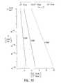
- FIG. 7Cis a graph plotting tunneling currents versus the applied electric fields (reciprocal applied electric field shown) for an number of barrier heights.
- FIG. 8illustrates a block diagram of an embodiment of an electronic system 801 according to the teachings of the present invention.
- FIG. 9is a table which provides relevant data on the barrier heights, energy gaps, dielectric constants and electron affinities of a wide variety of metal oxides that could be used as asymmetric tunnel barriers according to the teachings of the present invention.
- FIG. 10illustrates a block diagram of an embodiment of an electronic system according to the teachings of the present invention.
- wafer and substrateare interchangeably used to refer generally to any structure on which integrated circuits are formed, and also to such structures during various stages of integrated circuit fabrication. Both terms include doped and undoped semiconductors, epitaxial layers of a semiconductor on a supporting semiconductor or insulating material, combinations of such layers, as well as other such structures that are known in the art.
- horizontalas used in this application is defined as a plane parallel to the conventional plane or surface of a wafer or substrate, regardless of the orientation of the wafer or substrate.
- verticalrefers to a direction perpendicular to the horizontal as defined above. Prepositions, such as “on”, “side” (as in “sidewall”), “higher”, “lower”, “over” and “under” are defined with respect to the conventional plane or surface being on the top surface of the wafer or substrate, regardless of the orientation of the wafer or substrate.
- the present inventiondescribes the use of asymmetrical metal oxide inter-poly dielectric insulators, formed by atomic layer deposition (ALD), between the control gate and the floating gate of non-volatile memory cells.
- ALDatomic layer deposition
- FIG. 2An example is shown in FIG. 2 for a planar structure, or horizontal non-volatile memory cell.
- This non-volatile memory cell, as described herein,can then be implemented in a number of programmable array type logic and/or memory devices according to the teachings of the present invention.
- ALDatomic layer deposition
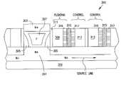
- FIG. 2illustrates one embodiment of a floating gate transistor, or non-volatile memory cell 200 , according to the teachings of the present invention.
- the non-volatile memory cell 200includes a first source/drain region 201 and a second source/drain region 203 separated by a channel region 205 in a substrate 206 .
- a floating gate 209opposes the channel region 205 and is separated therefrom by a gate oxide 211 .
- a control gate 213opposes the floating gate 209 .
- the control gate 213is separated from the floating gate 209 by an asymmetrical low tunnel barrier intergate insulator 215 .
- the asymmetrical low tunnel barrier intergate insulator 215includes an asymmetrical metal oxide insulator which is aluminum oxide (Al 2 O 3 ).
- the asymmetrical low tunnel barrier intergate insulator 215includes an asymmetrical transition metal oxide selected from the group consisting of Ta 2 O 5 , TiO 2 , ZrO 2 , and Nb 2 O 5 .
- the asymmetrical low tunnel barrier intergate insulator 215includes an asymmetrical Perovskite oxide tunnel barrier selected from the group consisting of SrBi 2 Ta 2 O 3 , SrTiO 3 , PbTiO 3 , and PbZrO 3
- the floating gate 209includes a polysilicon floating gate 209 having a metal layer 216 formed thereon in contact with the asymmetrical low tunnel barrier intergate insulator 215 .
- the control gate 213includes a polysilicon control gate 213 having a metal layer 217 , having a work function different from the metal layer 216 formed on the floating gate 209 , formed thereon in contact with the asymmetrical low tunnel barrier intergate insulator 215 .
- metal layer 216is formed of the same metal material used to form the asymmetrical metal oxide inter-poly insulator 215 .
- the non-volatile memory cellas described herein, can then be implemented in a number of programmable array type logic and/or memory devices according to the teachings of the present invention.
- FIG. 3illustrates another embodiment of a floating gate transistor, or non-volatile memory cell 300 , according to the teachings of the present invention.
- the non-volatile memory cell 300includes a vertical non volatile memory cell 300 .
- the non-volatile memory cell 300has a first source/drain region 301 formed on a substrate 306 .
- a body region 307 including a channel region 305is formed on the first source/drain region 301 .
- a second source/drain region 303is formed on the body region 307 .
- a floating gate 309opposes the channel region 305 and is separated therefrom by a gate oxide 311 .
- a control gate 313opposes the floating gate 309 . According to the teachings of the present invention, the control gate 313 is separated from the floating gate 309 by an asymmetrical low tunnel barrier intergate insulator 315 .
- low tunnel barrier intergate insulator 315includes an asymmetrical metal oxide insulator which is aluminum oxide (Al 2 O 3 ).
- the asymmetrical low tunnel barrier intergate insulator 315includes an asymmetrical transition metal oxide selected from the group consisting of Ta 2 O 5 , TiO 2 , ZrO 2 , and Nb 2 O 5 .
- the low tunnel barrier intergate insulator 315includes an asymmetrical Perovskite oxide tunnel barrier selected from the group consisting of SrBi 2 Ta 2 O 3 , SrTiO 3 , PbTiO 3 , and PbZrO 3 .
- the floating gate 309includes a polysilicon floating gate 309 having a metal layer 316 formed thereon in contact with the asymmetrical low tunnel barrier intergate insulator 315 .
- the control gate 313includes a polysilicon control gate 313 having a metal layer 317 , having a work function different from the metal layer 316 formed on the floating gate 309 , formed thereon in contact with the asymmetrical low tunnel barrier intergate insulator 315 .
- the non-volatile memory cellas described herein, can then be implemented in a number of programmable array type logic and/or memory devices according to the teachings of the present invention.
- the floating gate 309includes a vertical floating gate 309 formed alongside of the body region 307 .
- the control gate 313includes a vertical control gate 313 formed alongside of the vertical floating gate 309 .
- the floating gate 309 and control gate 313 orientation shown in FIG. 3is just one embodiment for a vertical non volatile memory cell 300 , according to the teachings of the present invention.
- the floating gateincludes a horizontally oriented floating gate formed alongside of the body region.
- the control gateincludes a horizontally oriented control gate formed above the horizontally oriented floating gate.
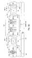
- FIG. 4is a perspective view illustrating an array of silicon pillars 400 - 1 , 400 - 2 , 400 - 3 , . . . , 400 -N, formed on a substrate 406 as used in one embodiment according to the teachings of the present invention.
- the substratescan be (i) conventional p-type bulk silicon or p-type epitaxial layers on p+ wafers, (ii) silicon on insulator formed by conventional SIMOX, wafer bonding and etch back or silicon on sapphire, or (iii) small islands of silicon on insulator utilizing techniques such as described in more detail in U.S. Pat. No. 5,691,230, by Leonard Forbes, entitled “Technique for Producing Small Islands of Silicon on Insulator,” issued Nov. 25, 1997, which is incorporated herein by reference.
- each pillar in the array of silicon pillars 400 - 1 , 400 - 2 , 400 - 3 , . . . , 400 -Nincludes a first source/drain region 401 and a second source/drain region 403 .
- the first and the second source/drain regions, 401 and 403are separated by a body region 407 including channel regions 405 .
- a number of trenches 430separate adjacent pillars in the array of silicon pillars 400 - 1 , 400 - 2 , 400 - 3 , . . . , 400 -N.
- Trenches 430are referenced in connection with the discussion which follows in connection with FIGS. 5A–5E .
- FIGS. 5A–5Eare cross sectional views taken along cut line 5 — 5 from FIG. 4 .
- FIG. 5Aillustrates one such embodiment of the present invention.
- FIG. 5Aillustrates a first source/drain region 501 and second source/drain region 503 for a non-volatile memory cell 500 formed according to the teachings of the present invention.
- the first and second source/drain regions, 501 and 503are contained in a pillar of semiconductor material, and separated by a body region 507 including channel regions 505 .
- FIGS. 5Aillustrates one such embodiment of the present invention.
- FIG. 5Aillustrates a first source/drain region 501 and second source/drain region 503 for a non-volatile memory cell 500 formed according to the teachings of the present invention.
- the first and second source/drain regions, 501 and 503are contained in a pillar of semiconductor material, and separated by a body region 507 including channel regions 505 .
- the first source/drain region 501is integrally connected to a buried sourceline 525 .
- the buried sourceline 525is be formed of semiconductor material which has the same doping type as the first source/drain region 501 .
- the sourceline 525is formed of semiconductor material of the same doping as the first source/drain region 501 , but is more heavily doped than the first source/drain region 501 .
- a pair of floating gates 509 - 1 and 509 - 2are formed in each trench 530 between adjacent pillars which form memory cells 500 - 1 and 500 - 2 .
- Each one of the pair of floating gates, 509 - 1 and 509 - 2respectively opposes the body regions 507 - 1 and 507 - 2 in adjacent pillars 500 - 1 and 500 - 2 on opposing sides of the trench 530 .
- a single control gate 513is shared by the pair of floating gates 509 - 1 and 509 - 2 on opposing sides of the trench 530 .
- the shared single control gate 513can include an integrally formed control gate line.
- an integrally formed control gate line 513can be one of a plurality of control gate lines which are each independently formed in the trench, such as trench 530 , below the top surface of the pillars 500 - 1 and 500 - 2 and between the pair of floating gates 509 - 1 and 509 - 2 .
- each floating gatee.g. 509 - 1 and 509 - 2 , includes a vertically oriented floating gate having a vertical length of less than 100 nanometers.
- a pair of floating gates 509 - 1 and 509 - 2are formed in each trench 530 between adjacent pillars which form memory cells 500 - 1 and 500 - 2 .
- Each one of the pair of floating gates, 509 - 1 and 509 - 2respectively opposes the body regions 507 - 1 and 507 - 2 in adjacent pillars 500 - 1 and 500 - 2 on opposing sides of the trench 530 .
- a plurality of control gate linesare again formed in trenches, e.g. trench 530 , below the top surface of the pillars, 500 - 1 and 500 - 2 , and between the pair of floating gates 509 - 1 and 509 - 2 .
- each trenche.g. 530
- Each one of the pair of control gate lines 513 - 1 and 513 - 2addresses the floating gates, 509 - 1 and 509 - 2 respectively, on opposing sides of the trench 530 .
- the pair of control gate lines, or control gates 513 - 1 and 513 - 2are separated by an insulator layer.
- a pair of floating gates 509 - 1 and 509 - 2are again formed in each trench 530 between adjacent pillars which form memory cells 500 - 1 and 500 - 2 .
- Each one of the pair of floating gates, 509 - 1 and 509 - 2respectively opposes the body regions 507 - 1 and 507 - 2 in adjacent pillars 500 - 1 and 500 - 2 on opposing sides of the trench 530 .
- the plurality of control gate linesare disposed vertically above the floating gates. That is, in one embodiment, the control gate lines are located above the pair of floating gates 509 - 1 and 509 - 2 and not fully beneath the top surface of the pillars 500 - 1 and 500 - 2 . In the embodiment of FIG. 5C , each pair of floating gates, e.g. 509 - 1 and 509 - 2 , in a given trench shares a single control gate line, or control gate 513 .
- a pair of floating gates 509 - 1 and 509 - 2are formed in each trench 530 between adjacent pillars which form memory cells 500 - 1 and 500 - 2 .
- Each one of the pair of floating gates, 509 - 1 and 509 - 2respectively opposes the body regions 507 - 1 and 507 - 2 in adjacent pillars 500 - 1 and 500 - 2 on opposing sides of the trench 530 .
- the plurality of control gate linesare disposed vertically above the floating gates. That is, in one embodiment, the control gate lines are located above the pair of floating gates 509 - 1 and 509 - 2 and not fully beneath the top surface of the pillars 500 - 1 and 500 - 2 . However, in the embodiment of FIG. 5D , each one of the pair of floating gates, e.g. 509 - 1 and 509 - 2 , is addressed by an independent one of the plurality of control lines or control gales, shown in FIG. 5D as 513 - 1 and 513 - 2 .
- a single floating gate 509is formed in each trench 530 between adjacent pillars which form memory cells 500 - 1 and 500 - 2 .
- the single floating gate 509can be either a vertically oriented floating gate 509 or a horizontally oriented floating gate 509 formed by conventional processing techniques, or can be a horizontally oriented floating gate 509 formed by a replacement gate technique such as described in a copending application, entitled “Flash Memory with Ultrathin Vertical Body Transistors,” by Leonard Forbes and Kie Y. Ahn, application Ser. No. 09/780,169.
- the floating gate 509has a vertical length facing the body region 505 of less than 100 nm.
- the floating gate 509has a vertical length facing the body region 505 of less than 50 nm.
- the floating gate 509is shared, respectively, with the body regions 507 - 1 and 507 - 2 , including channel regions 505 - 1 and 505 - 2 , in adjacent pillars 500 - 1 and 500 - 2 located on opposing sides of the trench 530 .
- the control gate 513includes a horizontally oriented control gate 513 formed above the horizontally oriented floating gate 509 .
- the floating gates 509are separated from the control gate lines, or control gates 513 with an asymmetrical low tunnel barrier intergate insulator in accordance with the descriptions given above in connection with FIG. 3 .
- the modifications hereare to use tunneling through the inter-poly dielectric to realize flash memory devices.
- the vertical devicesinclude an extra flexibility in that the capacitors, e.g. gate oxide and intergate insulator, are easily fabricated with different areas. This readily allows the use of very high dielectric constant inter-poly dielectric insulators with lower tunneling barriers.
- FIGS. 6A–6Dillustrate that a number of address coincidence schemes can be used together with the present invention.
- FIG. 6Aillustrates a NOR flash memory array 610 having a number of non-volatile memory cells 600 - 1 , 600 - 2 , 600 - 3 , using a coincidence address array scheme.
- FIG. 6Ashows a sourceline 625 coupled to a first source/drain region 601 in each of the number of non-volatile memory cells 600 - 1 , 600 - 2 , 600 - 3 .
- the sourcelineis shown oriented in a first selected direction in the flash memory array 610 .
- FIG. 6Aa number of control gate lines 630 are shown oriented in a second selected direction in the flash memory array 610 .
- the number of control gate lines 630are coupled to, or integrally formed with the control gates 613 for the number of non-volatile memory cells 600 - 1 , 600 - 2 , 600 - 3 .
- the second selected directionis orthogonal to the first selected direction.
- FIG. 6Ashows a number of bitlines 635 oriented in a third selected direction in the flash memory array 610 . As shown in FIG.
- the number of bitlinesare coupled to the second source/drain regions in the number of non-volatile memory cells 600 - 1 , 600 - 2 , 600 - 3 .
- the third selected directionis parallel to the second selected direction and the number of control gate lines 630 serve as address lines.
- the flash memory array 610includes a number of backgate or substrate/well bias address lines 640 coupled to the substrate.
- FIGS. 6B–6Dillustrate of top view for three different coincidence address scheme layouts suitable for use with the present invention.
- FIG. 6Bprovides the top view layout of the coincidence address scheme described in connection with FIG. 6A . That is, FIG. 6B illustrates a number of sourcelines 625 oriented in a first selected direction, a number of control gate lines 630 oriented in a second selected direction, and a, number of bitlines 635 oriented in a third selected direction for the flash memory array 600 .
- the second and third selected directionare parallel to one another and orthogonal to the first selected direction such that the number of control gate lines 630 serve as address lines.
- FIG. 6Cprovides the top view layout of another coincidence address scheme according to the teachings of the present invention.
- FIG. 6Cillustrates a number of sourcelines 625 oriented in a first selected direction, a number of control gate lines 630 oriented in a second selected direction, and a number of bitlines 635 oriented in a third selected direction for the flash memory array 600 .
- the first selected direction and the third selected directionare parallel to one another and orthogonal to the second selected direction.
- the number of control gate lines 630again serve as address lines.
- FIG. 6Dprovides the top view layout of yet another coincidence address scheme according to the teachings of the present invention.
- FIG. 6Dillustrates a number of sourcelines 625 oriented in a first selected direction, a number of control gate lines 630 oriented in a second selected direction, and a number of bitlines 635 oriented in a third selected direction for the flash memory array 600 .
- the first selected direction and the second selected directionare parallel to one another and orthogonal to the third selected direction.
- the number of bitlines 635serve as address lines.
- writecan still be achieved by hot electron injection and/or, according to the teachings of the present invention, tunneling from the control gate to the floating gate.
- block eraseis accomplished by driving the control gates with a relatively large positive voltage and tunneling from the metal on top of the floating gate to the metal on the bottom of the control gate.
- FIG. 7Ais an energy band diagram illustrating the band structure at vacuum level with the asymmetrical low tunnel barrier inter-poly insulator according to the teachings of the present invention.
- FIG. 7Ais useful in illustrating the reduced tunnel barrier off of the floating gate to the control gate and for illustrating the respective capacitances of the structure according to the teachings of the present invention.
- FIG. 7Ashows the band structure of the silicon substrate, e.g. channel region 701 , silicon dioxide gate insulator, e.g. gate oxide 703 , polysilicon floating gate 705 , the asymmetrical low tunnel barrier inter-poly dielectric 707 , between metal plates 709 and 711 , and then the polysilicon control gate 713 , according to the teachings of the present invention.
- the design considerations involvedare determined by the dielectric constant, thickness and tunneling barrier height of the asymmetrical inter-poly dielectric insulator 707 relative to that of the silicon dioxide gate insulator, e.g. gate oxide 703 .
- the tunneling probability through the inter-poly dielectric 707is an exponential function of both the barrier height and the electric field across this dielectric.
- FIG. 7Ashows the asymmetrical tunnel barriers, formed by atomic layer deposition (ALD), used for easy erase. Erase is achieved by the use of positive control gate voltages through the low tunnel barrier.
- ALDatomic layer deposition
- readutilizes positive control gate voltages with n-channel enhancement mode devices as described in the above referenced, copending applications, by the same inventors, entitled “FLASH MEMORY DEVICES WITH METAL OXIDE AND/OR LOW TUNNEL BARRIER INTERPLOY INSULATORS,” application Ser. No.
- readutilizes negative control gate voltages with n-channel depletion mode devices as described in the above referenced, copending application, by the same inventors, entitled “PROGRAMMABLE ARRAY TYPE LOGIC AND/OR MEMORY DEVICES WITH METAL OXIDE AND/OR LOW ASYMMETRICAL TUNNEL BARRIER INTERPLOY INSULATORS,” application Ser. No. 09/943,134.
- readutilizes negative control gate voltages with p-channel enhancement mode devices as described in the above referenced, copending application, by the same inventors, entitled “PROGRAMMABLE ARRAY TYPE LOGIC OR MEMORY WITH P-CHANNEL DEVICES AND ASYMMETRICAL TUNNEL BARRIERS,” application Ser. No. 10/028,001.
- Programmingis accomplished by channel hot electron injection with n-channel devices and/or electron injection from the control gate for both n-channel and p-channel devices and may or may not utilize positive substrate, well, or body bias.
- FIG. 7Bis an energy band diagram illustrating the band structure during an erase operation of electrons from the floating gate 705 to the control gate 713 across the low tunnel barrier inter-poly insulator 707 according to the teachings of the present invention.
- FIG. 7Bis similarly useful in illustrating the reduced tunnel barrier off of the floating gate 705 to the control gate 713 and for illustrating the respective capacitances of the structure according to the teachings of the present invention.
- the electric fieldis determined by the total voltage difference across the structure, the ratio of the capacitances (see FIG. 7A ), and the thickness of the asymmetrical inter-poly dielectric 707 .
- the lower electric field in the aluminum oxide inter-poly insulator 707 for the same current densityreflects the lower tunneling barrier of approximately 2 eV, shown in FIG. 7B , as opposed to the 3.2 eV tunneling barrier of silicon oxide 703 , also illustrated in FIG. 7B .
- FIG. 7Cis a graph plotting tunneling currents versus the applied electric fields (reciprocal applied electric field shown) for a number of barrier heights.
- FIG. 7Cillustrates the dependence of the tunneling currents on electric field (reciprocal applied electric field) and barrier height.
- the fraction of voltage across the asymmetrical inter-poly or asymmetrical intergate insulator, ⁇ V 2can be increased by making the area of the intergate capacitor, C 2 , (e.g. intergate insulator 707 ) smaller than the area of the transistor gate capacitor, C 1 (e.g. gate oxide 703 ). This would be required with high dielectric constant intergate dielectric insulators 707 and is easily realized with the vertical floating gate structures described above in connection with FIGS. 3 , and 5 A– 5 E.
- this disclosuredescribes the use of asymmetrical tunnel barriers formed by atomic layer deposition (ALD) and specifically low tunnel barriers during erase, to make erase of flash memory type devices easier.
- ALDatomic layer deposition
- the silicon oxidepresents a very high 3.2 eV barrier and high electric fields are required.
- the combination of very high electric fields and damage by hot electron collisions in the oxideresult in a number of operational problems like soft erase error, reliability problems of premature oxide breakdown and a limited number of cycles of write and erase.
- the tunneling currentsdepend exponentially on the barrier heights.
- An asymmetrical barrier, as shown in FIG. 7Apresents a low barrier for erase but can present a higher barrier during read and/or write operations when tunneling is not desired.
- asymmetrical barrierscan be achieved various ways, one technique is to use different metal contact plates, with the upper plate on the inter-poly or intergate insulator being a metal like platinum with a large work function as described above in the referenced, copending application, by the same inventors, entitled “PROGRAMMABLE ARRAY LOGIC OR MEMORY DEVICES WITH ASYMMETRICAL TUNNEL BARRIERS,” application Ser. No. 09/943,134.
- ALD processesAs is well-known to those in the field, the literature describing ALD oxide processes is quite large and still expanding rapidly. Within reasonable constraints imposed by chemical and physical properties of component metals and their oxides, ALD processes can be developed for producing an even wider range of single and multi-component oxide thin films. A few examples of ALD processes for forming some useful oxides for tunnel barriers and other applications are given next.
- ALD processusing TMA to form Al precursor layers and oxidizing them with water
- AlO x layersat 150–200 degrees Celsius for use in advanced gap and tunnel junction devices.
- Alumina films, grown on substrates as diverse as Si, Ta and NiFewere amorphous, conformal, stoichiometric (to within 2 at. %, pure ( ⁇ 5 at. % hydrogen and ⁇ 1 at. % other impurities), smooth (R A ⁇ 2 angstroms) with controllable levels of stress. Extraordinary levels of thickness control (to within 1 angstrom) have been achieved upon using ALD to form ultra-thin Al 2 O 3 and SiO 2 films on BN particles.
- Such oxide coatingscan be employed to modify surface energies in order to increase loading of BN particles in polymer films for packaging.
- Hf(NO 3 ) 4could be used for making CVD HfO 2 films on silicon at temperatures as low as 300 degrees Celsius. Such films contain excess oxygen and that can apparently be removed by heating in nitrogen at higher temperatures. Similar findings were made forming TiO 2 and ZrO 2 films. The authors opine that these oxides could be made by ALCVD, using Group IV nitrate precursors. Due to the low ALD operable temperatures, it is possible to conduct detailed in situ deposition rate studies in many instances in order to more precisely define metal oxide thicknesses. For example, Aarik et al. (see generally, J. Aarik et al, “Anomalous effect of temperature on atomic layer deposition of titanium dioxide”, Jour. Crystal Growth 220, pp.
- transition metal oxidescan also be deposited for use as tunnel barriers. Such processes involve depositing transition metal alloy precursor layers followed by oxidation, followed again by addition of the alloy precursor layer and so on until the desired mixed oxide tunnel junction thickness is reached.
- certain perovskite oxide oxide filmscan be formed by first using ALD to form the desired amorphous oxide composition and then heating to produce the perovskite crystal structure. Clearly formation of such mixed oxide films is more complex and will not be described here.
- FIG. 8graphically illustrates the dependence of the barrier height for current injection on the work function and electron affinity of a given, homogeneous dielectric film.
- FIG. 9is a table which provides relevant data on the barrier heights, energy gaps, dielectric constants and electron affinities of a wide variety of metal oxides that could be used as asymmetric tunnel barriers according to the teachings of the present invention. (See generally, H. F. Luan et al., “High quality Ta2O5 gate dielectrics with Tox equil. 10 Angstroms,”IEDM Tech. Digest, pp. 141–144, 1999; J.
- Robertson et al.“Schottky barrier heights of tantalum oxide, barium strontium titanate, lead titanate and strontium bismuth tantalate,” App. Phys. Lett., Vol. 74, No. 8, pp. 1168–1170, February 1999; J. Robertson, “Band offsets of wide-band-gap oxides and implications for future electronic devices,” J. Vac. Sci. Technol. B, Vol. 18, No. 3, pp. 1785–1791, 2000; Xin Guo et al., “High quality ultra-thin (1.5 nm) TiO2/Si3N4 gate dielectric for deep submicron CMOS technology,” IEDM Tech. Digest, pp.
- Barriers of Al 2 O 3 formed on Alwill exhibit some minor barrier height difference when injecting electrons from the inner and outer electrodes.
- the barrier height differencewill be at most 0.1 eV and will arise from small differences in oxide composition at the interfaces. (See generally copending application, entitled “PROGRAMMABLE ARRAY TYPE LOGIC OR MEMORY WITH P-CHANNEL DEVICES AND ASYMMETRICAL TUNNEL BARRIERS,” application Ser. No. 10/028,001m, for a complete explanation). Moreover, such small differences will not interfere with the proper functioning of the devices of this disclosure.
- Formation of Al/Ta 2 O 5 /Al tunnel barrierscan be formed with a barrier height of about 2 eV. See FIGS. 8 and 9 .
- processes for producing ultra-thin films of Ta 2 O 5 that are suitable for tunnel barriersare known. See, for example, the work of Kim et al. (see generally, Y. S. Kim et al., “Effect of rapid thermal annealing on the structure and the electrical properties of atomic layer deposited Ta 2 O 5 films”, Jour. Korean Phys. Soc. 37 (6), pp. 975–979 (2000)) cited above. Note that it may not be necessary to maximize the dielectric constant of this oxide for the present applications although such maximization is desirable for building useful, minimal area DRAM storage capacitors.
- a very limited intermixing of Al and Ta oxides at the ALD formed interfacecan develop unless a few steps are taken to minimize this. For example, minimization of the ALD process temperature.
- first forming a monolayer of Al 2 O 3by exposing the water precursor before the Ta(OEt) 5 precursor. Intermixing of a monolayer or two at this interface can also be accepted (provided it is reproducible from wafer-to-wafer, run-to-run, etc.). More detailed studies have shown that the tunnel current-barrier thickness characteristics are better described in terms of an “average barrier height.”
- the large bulk, if not all, of the tunnel barrierwill consist of a layer of Ta 2 O 5 with a thickness that could lie in the range of perhaps 20 to 50 Angstroms or more.
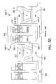
- FIG. 10illustrates a block diagram of an embodiment of an electronic system 1001 according to the teachings of the present invention.
- the system 1001includes a memory device 1000 which has an array of memory cells 1002 , address decoder 1004 , row access circuitry 1006 , column access circuitry 1008 , control circuitry 1010 , and input/output circuit 1012 .
- the circuit 1001includes a processor 1014 , or memory controller for memory accessing.
- the memory device 1000receives control signals from the processor 1014 , such as WE*, RAS* and CAS* signals over wiring or metallization lines.
- the memory device 1000is used to store data which is accessed via I/O lines.
- At least one of the processor 1014 or memory device 1000has a memory cell formed according to the embodiments of the present invention. That is, at least one of the processor 1014 or memory device 1000 includes an asymmetrical low tunnel barrier inter-poly insulator according to the teachings of the present invention.
- FIG. 10illustrates an embodiment for electronic system circuitry in which the novel memory cells of the present invention are used.
- the illustration of system 1001is intended to provide a general understanding of one application for the structure and circuitry of the present invention, and is not intended to serve as a complete description of all the elements and features of an electronic system using the novel memory cell structures.
- the inventionis equally applicable to any size and type of memory device 1000 using the novel memory cells of the present invention and is not intended to be limited to that described above.
- such an electronic systemcan be fabricated in single-package processing units, or even on a single semiconductor chip, in order to reduce the communication time between the processor and the memory device.
- Applications containing the novel memory cell of the present invention as described in this disclosureinclude electronic systems for use in memory modules, device drivers, power modules, communication modems, processor modules, and application-specific modules, and may include multilayer, multichip modules.
- Such circuitrycan further be a subcomponent of a variety of electronic systems, such as a clock, a television, a cell phone, a personal computer, an automobile, an industrial control system, an aircraft, and others.
- Asymmetrical low barrier tunnel insulatorsare described between the floating gate and control gate in a flash memory type devices to form programmable array logic and memory devices.
- the asymmetrical low barrier insulators⁇ 2.0 eV, are formed by atomic layer deposition (ALD). While the amount of charge stored on the floating gate is small the transistor provides gain and charge multiplication resulting in a large output signal and ease of reading the stored data. If there is an adverse capacitance ratio due to a large difference of dielectric constants then the vertical gate structures described previously can be employed.
- the asymmetrical low tunnel barrier inter-poly insulators of the present inventionavoid the large barriers to electron tunneling or hot electron injection presented by the silicon oxide-silicon interface, 3.2 eV, which result in slow write and erase speeds even at very high electric fields.
- the present inventionalso avoids the combination of very high electric fields and damage by hot electron collisions in the which oxide result in a number of operational problems like soft erase error, reliability problems of premature oxide breakdown and a limited number of cycles of write and erase.
- the asymmetrical low tunnel barrier interploy dielectric insulator erase approach, of the present inventionremedies the above mentioned problems of having a rough top surface on the polysilicon floating gate which results in, poor quality inter-poly oxides, sharp points, localized high electric fields, premature breakdown and reliability problems.
- ALDatomic layer deposition
Landscapes
- Non-Volatile Memory (AREA)
- Semiconductor Memories (AREA)
Abstract
Description
J=Bexp(−Eo/E)
where E is the electric field across the inter-poly
- (a) Films can be grown at low (<300 to 400 degrees Celsius) temperatures.
- (b) Films can be grown on a variety of substrate materials, including a wide range of inorganic (e.g., silicon, glass, oxide and nitride) to metallic surfaces.
- (c) Films can be comprised of single (e.g., Al2O3) and multiple metal components.
- (d) The thicknesses of the oxide films can be controlled to within a thickness of 1 monolayer. Their thickness uniformities are exceptionally high.
- (e) Films are chemically homogeneous, uniform and have a strong tendency to form the most stable compositions in their respective metal-oxygen systems. For example, Ta2O5forms in the Ta—O system.
- (f) Even ultra-thin films exhibit excellent step and sidewall coverage. This will be particularly advantageous for enhancing the quality of so-called “vertical transistor” devices. Step coverage difficulties are relatively less demanding in “horizontally configured” transistors.
- (g) Control of the bottom metal layer thickness and uniformity are less demanding, provided the metal is sufficiently conductive throughout. In other words, the prime function of the metal, in combination with the appropriate oxide, is to produce a lower tunnel barrier relative to conventional barriers such as Si/SiO2.
- (h) Films are excellent insulators with high breakdown strengths.
- (i) Films have high dielectric constants as formed at low temperatures. This invention does not require that the oxides have very high dielectric constants. However, if necessary, many of the ALD oxides can be subsequently heat treated to substantially increase their dielectric constants. Such changes typically result from minute micro-structural changes, i.e., transformations from amorphous to nano-crystalline phases.
- (i) Use a low energy, inert ion plasma in the auxiliary chamber to sputter clean residual oxides, etc. from the poly-Si surfaces previously fabricated on the device wafer.
- (ii) Deposit an aluminum contact layer over the poly-Si. This layer is presumably ten to hundreds of angstroms thick, as needed to insure good coverage of the poly-Si.
- (iii) Transfer the device wafer to the ALD processing chamber under a vacuum sufficient to prevent inadvertent oxidation.
- (iv) Produce the desired Al2O3layer via an ALD. Several precursor chemistries are available, as indicated by the few examples in the references cited above in connection with the discussion on Al2O3. For example, the low temperature process described by Paranjpe et al. (see generally, A. Paranjpe et al., “Atomic layer deposition of AlOxfor thin film head gap applications”, Jour. Electrochem. Soc. 148 (9), G465–G471 (2001)) looks attractive for this purpose since it was developed to operate at temperatures in the 150–200 degrees Celsius range, using trimethylaluminum and water as precursors. As such, Al2O3films as thin as 5 to 10 Angstroms have been shown to be continuous with excellent insulating properties.
- (v) Transfer the device wafer back to the auxiliary chamber and deposit the top aluminum electrode layer.
- (vi) Remove the wafer from the system for further processing, e.g., addition of silicon control layer, patterning, etc.
- (i) Use a low energy, inert ion plasma in the auxiliary chamber to sputter clean residual exodies, etc. from the poly-Si surfaces previously fabricated on the device wafer.
- (ii) Deposit an aluminum contact layer over the poly-Si. This layer is presumably ten to hundreds of angstroms thick, as needed to insure good coverage of the poly-Si.
- (iii) Transfer the device wafer to the ALD processing chamber, under a vacuum sufficient to prevent inadvertent oxidation.
- (iv) Produce the desired Ta2O5layer via an ALD process such as the one just cited, using a Ta(OEt)5and water as precursors and a temperature of 300 degrees Celsius or lower, if possible, in order to prevent inadvertent Al recrystallization and growth. Formed in this way, the dielectric constant of the oxide will be approximately 22–24.
- (v) Transfer the device wafer back to the auxiliary chamber and deposit the top aluminum electrode layer.
- (vi) Remove the wafer from the system for further processing, e.g., addition of silicon control layer, patterning, etc.
Claims (32)
Priority Applications (6)
| Application Number | Priority Date | Filing Date | Title |
|---|---|---|---|
| US10/081,818US7476925B2 (en) | 2001-08-30 | 2002-02-20 | Atomic layer deposition of metal oxide and/or low asymmetrical tunnel barrier interploy insulators |
| US10/929,986US7473956B2 (en) | 2001-08-30 | 2004-08-30 | Atomic layer deposition of metal oxide and/or low assymmetrical tunnel barrier interpoly insulators |
| US11/380,599US7508025B2 (en) | 2001-08-30 | 2006-04-27 | Atomic layer deposition of metal oxide and/or low asymmetrical tunnel barrier interpoly insulators |
| US11/704,458US7446368B2 (en) | 2001-08-30 | 2007-02-09 | Deposition of metal oxide and/or low asymmetrical tunnel barrier interpoly insulators |
| US11/708,438US7465983B2 (en) | 2001-08-30 | 2007-02-20 | Low tunnel barrier insulators |
| US11/728,671US7504687B2 (en) | 2001-08-30 | 2007-03-27 | Atomic layer deposition of metal oxide and/or low asymmetrical tunnel barrier interpoly insulators |
Applications Claiming Priority (2)
| Application Number | Priority Date | Filing Date | Title |
|---|---|---|---|
| US09/943,134US7042043B2 (en) | 2001-08-30 | 2001-08-30 | Programmable array logic or memory devices with asymmetrical tunnel barriers |
| US10/081,818US7476925B2 (en) | 2001-08-30 | 2002-02-20 | Atomic layer deposition of metal oxide and/or low asymmetrical tunnel barrier interploy insulators |
Related Parent Applications (2)
| Application Number | Title | Priority Date | Filing Date |
|---|---|---|---|
| US09/943,134Continuation-In-PartUS7042043B2 (en) | 2001-08-30 | 2001-08-30 | Programmable array logic or memory devices with asymmetrical tunnel barriers |
| US09/943,134DivisionUS7042043B2 (en) | 2001-08-30 | 2001-08-30 | Programmable array logic or memory devices with asymmetrical tunnel barriers |
Related Child Applications (2)
| Application Number | Title | Priority Date | Filing Date |
|---|---|---|---|
| US10/929,986DivisionUS7473956B2 (en) | 2001-08-30 | 2004-08-30 | Atomic layer deposition of metal oxide and/or low assymmetrical tunnel barrier interpoly insulators |
| US11/704,458ContinuationUS7446368B2 (en) | 2001-08-30 | 2007-02-09 | Deposition of metal oxide and/or low asymmetrical tunnel barrier interpoly insulators |
Publications (2)
| Publication Number | Publication Date |
|---|---|
| US20030045082A1 US20030045082A1 (en) | 2003-03-06 |
| US7476925B2true US7476925B2 (en) | 2009-01-13 |
Family
ID=34107110
Family Applications (6)
| Application Number | Title | Priority Date | Filing Date |
|---|---|---|---|
| US10/081,818Expired - LifetimeUS7476925B2 (en) | 2001-08-30 | 2002-02-20 | Atomic layer deposition of metal oxide and/or low asymmetrical tunnel barrier interploy insulators |
| US10/929,986Expired - LifetimeUS7473956B2 (en) | 2001-08-30 | 2004-08-30 | Atomic layer deposition of metal oxide and/or low assymmetrical tunnel barrier interpoly insulators |
| US11/380,599Expired - LifetimeUS7508025B2 (en) | 2001-08-30 | 2006-04-27 | Atomic layer deposition of metal oxide and/or low asymmetrical tunnel barrier interpoly insulators |
| US11/704,458Expired - LifetimeUS7446368B2 (en) | 2001-08-30 | 2007-02-09 | Deposition of metal oxide and/or low asymmetrical tunnel barrier interpoly insulators |
| US11/708,438Expired - LifetimeUS7465983B2 (en) | 2001-08-30 | 2007-02-20 | Low tunnel barrier insulators |
| US11/728,671Expired - LifetimeUS7504687B2 (en) | 2001-08-30 | 2007-03-27 | Atomic layer deposition of metal oxide and/or low asymmetrical tunnel barrier interpoly insulators |
Family Applications After (5)
| Application Number | Title | Priority Date | Filing Date |
|---|---|---|---|
| US10/929,986Expired - LifetimeUS7473956B2 (en) | 2001-08-30 | 2004-08-30 | Atomic layer deposition of metal oxide and/or low assymmetrical tunnel barrier interpoly insulators |
| US11/380,599Expired - LifetimeUS7508025B2 (en) | 2001-08-30 | 2006-04-27 | Atomic layer deposition of metal oxide and/or low asymmetrical tunnel barrier interpoly insulators |
| US11/704,458Expired - LifetimeUS7446368B2 (en) | 2001-08-30 | 2007-02-09 | Deposition of metal oxide and/or low asymmetrical tunnel barrier interpoly insulators |
| US11/708,438Expired - LifetimeUS7465983B2 (en) | 2001-08-30 | 2007-02-20 | Low tunnel barrier insulators |
| US11/728,671Expired - LifetimeUS7504687B2 (en) | 2001-08-30 | 2007-03-27 | Atomic layer deposition of metal oxide and/or low asymmetrical tunnel barrier interpoly insulators |
Country Status (1)
| Country | Link |
|---|---|
| US (6) | US7476925B2 (en) |
Cited By (6)
| Publication number | Priority date | Publication date | Assignee | Title |
|---|---|---|---|---|
| US20070090439A1 (en)* | 2005-05-27 | 2007-04-26 | Micron Technology, Inc. | Hafnium titanium oxide films |
| US20070170492A1 (en)* | 2005-02-23 | 2007-07-26 | Micron Technology, Inc. | Germanium-silicon-carbide floating gates in memories |
| US20090008697A1 (en)* | 2001-08-30 | 2009-01-08 | Micron Technology, Inc. | Sram cells with repressed floating gate memory, low tunnel barrier interpoly insulators |
| US20100039867A1 (en)* | 2008-08-15 | 2010-02-18 | Macronix International Co., Ltd. | Electrically Isolated Gated Diode Nonvolatile Memory |
| US20110220983A1 (en)* | 2006-03-31 | 2011-09-15 | Semiconductor Energy Laboratory Co., Ltd. | Method for deleting data from nand type nonvolatile memory |
| US9136457B2 (en) | 2006-09-20 | 2015-09-15 | Hypres, Inc. | Double-masking technique for increasing fabrication yield in superconducting electronics |
Families Citing this family (165)
| Publication number | Priority date | Publication date | Assignee | Title |
|---|---|---|---|---|
| US7554829B2 (en)* | 1999-07-30 | 2009-06-30 | Micron Technology, Inc. | Transmission lines for CMOS integrated circuits |
| US6852167B2 (en) | 2001-03-01 | 2005-02-08 | Micron Technology, Inc. | Methods, systems, and apparatus for uniform chemical-vapor depositions |
| US7253467B2 (en)* | 2001-06-28 | 2007-08-07 | Samsung Electronics Co., Ltd. | Non-volatile semiconductor memory devices |
| US7473959B2 (en)* | 2001-06-28 | 2009-01-06 | Samsung Electronics Co., Ltd. | Non-volatile semiconductor memory devices and methods of fabricating the same |
| DE10228768A1 (en)* | 2001-06-28 | 2003-01-16 | Samsung Electronics Co Ltd | Non-volatile floating trap storage device comprises a semiconductor substrate, a tunnel insulation layer on the substrate, a charge storage layer, a barrier insulation layer, and a gate electrode |
| US20060180851A1 (en)* | 2001-06-28 | 2006-08-17 | Samsung Electronics Co., Ltd. | Non-volatile memory devices and methods of operating the same |
| US8253183B2 (en) | 2001-06-28 | 2012-08-28 | Samsung Electronics Co., Ltd. | Charge trapping nonvolatile memory devices with a high-K blocking insulation layer |
| US7476925B2 (en)* | 2001-08-30 | 2009-01-13 | Micron Technology, Inc. | Atomic layer deposition of metal oxide and/or low asymmetrical tunnel barrier interploy insulators |
| US6778441B2 (en)* | 2001-08-30 | 2004-08-17 | Micron Technology, Inc. | Integrated circuit memory device and method |
| US7087954B2 (en)* | 2001-08-30 | 2006-08-08 | Micron Technology, Inc. | In service programmable logic arrays with low tunnel barrier interpoly insulators |
| US7012297B2 (en)* | 2001-08-30 | 2006-03-14 | Micron Technology, Inc. | Scalable flash/NV structures and devices with extended endurance |
| US7132711B2 (en)* | 2001-08-30 | 2006-11-07 | Micron Technology, Inc. | Programmable array logic or memory with p-channel devices and asymmetrical tunnel barriers |
| US6754108B2 (en)* | 2001-08-30 | 2004-06-22 | Micron Technology, Inc. | DRAM cells with repressed floating gate memory, low tunnel barrier interpoly insulators |
| US7135734B2 (en)* | 2001-08-30 | 2006-11-14 | Micron Technology, Inc. | Graded composition metal oxide tunnel barrier interpoly insulators |
| US8026161B2 (en)* | 2001-08-30 | 2011-09-27 | Micron Technology, Inc. | Highly reliable amorphous high-K gate oxide ZrO2 |
| US7042043B2 (en)* | 2001-08-30 | 2006-05-09 | Micron Technology, Inc. | Programmable array logic or memory devices with asymmetrical tunnel barriers |
| US7068544B2 (en)* | 2001-08-30 | 2006-06-27 | Micron Technology, Inc. | Flash memory with low tunnel barrier interpoly insulators |
| US7075829B2 (en)* | 2001-08-30 | 2006-07-11 | Micron Technology, Inc. | Programmable memory address and decode circuits with low tunnel barrier interpoly insulators |
| KR100398579B1 (en)* | 2001-10-30 | 2003-09-19 | 주식회사 하이닉스반도체 | Nonvolatile memory device and method for fabricating the same |
| US6953730B2 (en)* | 2001-12-20 | 2005-10-11 | Micron Technology, Inc. | Low-temperature grown high quality ultra-thin CoTiO3 gate dielectrics |
| US6784480B2 (en)* | 2002-02-12 | 2004-08-31 | Micron Technology, Inc. | Asymmetric band-gap engineered nonvolatile memory device |
| US6893984B2 (en)* | 2002-02-20 | 2005-05-17 | Micron Technology Inc. | Evaporated LaA1O3 films for gate dielectrics |
| DE10219116A1 (en)* | 2002-04-29 | 2003-11-13 | Infineon Technologies Ag | Integrated circuit arrangement with connection layers and associated manufacturing processes |
| US7045430B2 (en)* | 2002-05-02 | 2006-05-16 | Micron Technology Inc. | Atomic layer-deposited LaAlO3 films for gate dielectrics |
| US7589029B2 (en) | 2002-05-02 | 2009-09-15 | Micron Technology, Inc. | Atomic layer deposition and conversion |
| US7160577B2 (en)* | 2002-05-02 | 2007-01-09 | Micron Technology, Inc. | Methods for atomic-layer deposition of aluminum oxides in integrated circuits |
| US7205218B2 (en) | 2002-06-05 | 2007-04-17 | Micron Technology, Inc. | Method including forming gate dielectrics having multiple lanthanide oxide layers |
| US7135421B2 (en) | 2002-06-05 | 2006-11-14 | Micron Technology, Inc. | Atomic layer-deposited hafnium aluminum oxide |
| AU2003227514A1 (en)* | 2002-06-07 | 2003-12-22 | Oticon A/S | Feed-through process and amplifier with feed-through |
| US7221586B2 (en) | 2002-07-08 | 2007-05-22 | Micron Technology, Inc. | Memory utilizing oxide nanolaminates |
| US7221017B2 (en)* | 2002-07-08 | 2007-05-22 | Micron Technology, Inc. | Memory utilizing oxide-conductor nanolaminates |
| US7019353B2 (en)* | 2002-07-26 | 2006-03-28 | Micron Technology, Inc. | Three dimensional flash cell |
| US6921702B2 (en)* | 2002-07-30 | 2005-07-26 | Micron Technology Inc. | Atomic layer deposited nanolaminates of HfO2/ZrO2 films as gate dielectrics |
| US6884739B2 (en)* | 2002-08-15 | 2005-04-26 | Micron Technology Inc. | Lanthanide doped TiOx dielectric films by plasma oxidation |
| US6790791B2 (en)* | 2002-08-15 | 2004-09-14 | Micron Technology, Inc. | Lanthanide doped TiOx dielectric films |
| US7199023B2 (en)* | 2002-08-28 | 2007-04-03 | Micron Technology, Inc. | Atomic layer deposited HfSiON dielectric films wherein each precursor is independendently pulsed |
| US7084078B2 (en)* | 2002-08-29 | 2006-08-01 | Micron Technology, Inc. | Atomic layer deposited lanthanide doped TiOx dielectric films |
| US6833575B2 (en)* | 2002-08-29 | 2004-12-21 | Micron Technology, Inc. | Dopant barrier for doped glass in memory devices |
| KR100480622B1 (en)* | 2002-10-16 | 2005-03-31 | 삼성전자주식회사 | Semiconductor device having dielectric layer improved dielectric characteristic and leakage current and method for manufacturing the same |
| US7101813B2 (en)* | 2002-12-04 | 2006-09-05 | Micron Technology Inc. | Atomic layer deposited Zr-Sn-Ti-O films |
| US6958302B2 (en)* | 2002-12-04 | 2005-10-25 | Micron Technology, Inc. | Atomic layer deposited Zr-Sn-Ti-O films using TiI4 |
| US7192892B2 (en)* | 2003-03-04 | 2007-03-20 | Micron Technology, Inc. | Atomic layer deposited dielectric layers |
| US7135369B2 (en)* | 2003-03-31 | 2006-11-14 | Micron Technology, Inc. | Atomic layer deposited ZrAlxOy dielectric layers including Zr4AlO9 |
| US7183186B2 (en)* | 2003-04-22 | 2007-02-27 | Micro Technology, Inc. | Atomic layer deposited ZrTiO4 films |
| US6970053B2 (en)* | 2003-05-22 | 2005-11-29 | Micron Technology, Inc. | Atomic layer deposition (ALD) high permeability layered magnetic films to reduce noise in high speed interconnection |
| US7192824B2 (en)* | 2003-06-24 | 2007-03-20 | Micron Technology, Inc. | Lanthanide oxide / hafnium oxide dielectric layers |
| KR100471408B1 (en)* | 2003-06-30 | 2005-03-14 | 주식회사 하이닉스반도체 | Method for patterning a metal wire in semiconductor device |
| US7220665B2 (en)* | 2003-08-05 | 2007-05-22 | Micron Technology, Inc. | H2 plasma treatment |
| US8513634B2 (en)* | 2003-12-17 | 2013-08-20 | Samsung Electronics Co., Ltd. | Nonvolatile data storage, semicoductor memory device including nonvolatile data storage and method of forming the same |
| US20050276922A1 (en)* | 2004-06-10 | 2005-12-15 | Henry Bernhardt | Method of forming thin dielectric layers |
| JP2006005313A (en)* | 2004-06-21 | 2006-01-05 | Toshiba Corp | Semiconductor device and manufacturing method thereof |
| US7601649B2 (en)* | 2004-08-02 | 2009-10-13 | Micron Technology, Inc. | Zirconium-doped tantalum oxide films |
| US7081421B2 (en) | 2004-08-26 | 2006-07-25 | Micron Technology, Inc. | Lanthanide oxide dielectric layer |
| US7494939B2 (en) | 2004-08-31 | 2009-02-24 | Micron Technology, Inc. | Methods for forming a lanthanum-metal oxide dielectric layer |
| US7588988B2 (en) | 2004-08-31 | 2009-09-15 | Micron Technology, Inc. | Method of forming apparatus having oxide films formed using atomic layer deposition |
| US7473278B2 (en)* | 2004-09-16 | 2009-01-06 | Smith & Nephew, Inc. | Method of surface oxidizing zirconium and zirconium alloys and resulting product |
| KR100590568B1 (en)* | 2004-11-09 | 2006-06-19 | 삼성전자주식회사 | Multi-bit Flash Memory Device and Operation Method |
| US7235501B2 (en) | 2004-12-13 | 2007-06-26 | Micron Technology, Inc. | Lanthanum hafnium oxide dielectrics |
| US20060125030A1 (en)* | 2004-12-13 | 2006-06-15 | Micron Technology, Inc. | Hybrid ALD-CVD of PrxOy/ZrO2 films as gate dielectrics |
| US7709334B2 (en)* | 2005-12-09 | 2010-05-04 | Macronix International Co., Ltd. | Stacked non-volatile memory device and methods for fabricating the same |
| US7473589B2 (en)* | 2005-12-09 | 2009-01-06 | Macronix International Co., Ltd. | Stacked thin film transistor, non-volatile memory devices and methods for fabricating the same |
| US7642585B2 (en)* | 2005-01-03 | 2010-01-05 | Macronix International Co., Ltd. | Non-volatile memory cells, memory arrays including the same and methods of operating cells and arrays |
| US8264028B2 (en)* | 2005-01-03 | 2012-09-11 | Macronix International Co., Ltd. | Non-volatile memory cells, memory arrays including the same and methods of operating cells and arrays |
| US8482052B2 (en)* | 2005-01-03 | 2013-07-09 | Macronix International Co., Ltd. | Silicon on insulator and thin film transistor bandgap engineered split gate memory |
| US7315474B2 (en) | 2005-01-03 | 2008-01-01 | Macronix International Co., Ltd | Non-volatile memory cells, memory arrays including the same and methods of operating cells and arrays |
| US7863128B1 (en)* | 2005-02-04 | 2011-01-04 | Spansion Llc | Non-volatile memory device with improved erase speed |
| US7374964B2 (en)* | 2005-02-10 | 2008-05-20 | Micron Technology, Inc. | Atomic layer deposition of CeO2/Al2O3 films as gate dielectrics |
| US7492001B2 (en)* | 2005-03-23 | 2009-02-17 | Spansion Llc | High K stack for non-volatile memory |
| US7687409B2 (en) | 2005-03-29 | 2010-03-30 | Micron Technology, Inc. | Atomic layer deposited titanium silicon oxide films |
| US7365027B2 (en) | 2005-03-29 | 2008-04-29 | Micron Technology, Inc. | ALD of amorphous lanthanide doped TiOx films |
| US7662729B2 (en) | 2005-04-28 | 2010-02-16 | Micron Technology, Inc. | Atomic layer deposition of a ruthenium layer to a lanthanide oxide dielectric layer |
| US7279740B2 (en) | 2005-05-12 | 2007-10-09 | Micron Technology, Inc. | Band-engineered multi-gated non-volatile memory device with enhanced attributes |
| US7612403B2 (en)* | 2005-05-17 | 2009-11-03 | Micron Technology, Inc. | Low power non-volatile memory and gate stack |
| US7636257B2 (en)* | 2005-06-10 | 2009-12-22 | Macronix International Co., Ltd. | Methods of operating p-channel non-volatile memory devices |
| US7402850B2 (en)* | 2005-06-21 | 2008-07-22 | Micron Technology, Inc. | Back-side trapped non-volatile memory device |
| US7195999B2 (en)* | 2005-07-07 | 2007-03-27 | Micron Technology, Inc. | Metal-substituted transistor gates |
| US7829938B2 (en)* | 2005-07-14 | 2010-11-09 | Micron Technology, Inc. | High density NAND non-volatile memory device |
| US7927948B2 (en) | 2005-07-20 | 2011-04-19 | Micron Technology, Inc. | Devices with nanocrystals and methods of formation |
| US7446369B2 (en)* | 2005-08-04 | 2008-11-04 | Spansion, Llc | SONOS memory cell having high-K dielectric |
| US7763927B2 (en)* | 2005-12-15 | 2010-07-27 | Macronix International Co., Ltd. | Non-volatile memory device having a nitride-oxide dielectric layer |
| US7393736B2 (en)* | 2005-08-29 | 2008-07-01 | Micron Technology, Inc. | Atomic layer deposition of Zrx Hfy Sn1-x-y O2 films as high k gate dielectrics |
| KR100717768B1 (en)* | 2005-08-30 | 2007-05-11 | 주식회사 하이닉스반도체 | Capacitors for semiconductor devices and forming methods thereof, Non-volatile memory devices and manufacturing methods thereof |
| US8071476B2 (en) | 2005-08-31 | 2011-12-06 | Micron Technology, Inc. | Cobalt titanium oxide dielectric films |
| US7410910B2 (en) | 2005-08-31 | 2008-08-12 | Micron Technology, Inc. | Lanthanum aluminum oxynitride dielectric films |
| US7214994B2 (en)* | 2005-08-31 | 2007-05-08 | Micron Technology, Inc. | Self aligned metal gates on high-k dielectrics |
| US7629641B2 (en)* | 2005-08-31 | 2009-12-08 | Micron Technology, Inc. | Band engineered nano-crystal non-volatile memory device utilizing enhanced gate injection |
| US7429767B2 (en)* | 2005-09-01 | 2008-09-30 | Micron Technology, Inc. | High performance multi-level non-volatile memory device |
| US7572741B2 (en)* | 2005-09-16 | 2009-08-11 | Cree, Inc. | Methods of fabricating oxide layers on silicon carbide layers utilizing atomic oxygen |
| JP4928890B2 (en)* | 2005-10-14 | 2012-05-09 | 株式会社東芝 | Nonvolatile semiconductor memory device |
| US7697827B2 (en) | 2005-10-17 | 2010-04-13 | Konicek Jeffrey C | User-friendlier interfaces for a camera |
| US7972974B2 (en)* | 2006-01-10 | 2011-07-05 | Micron Technology, Inc. | Gallium lanthanide oxide films |
| US7709402B2 (en) | 2006-02-16 | 2010-05-04 | Micron Technology, Inc. | Conductive layers for hafnium silicon oxynitride films |
| KR100717770B1 (en)* | 2006-04-24 | 2007-05-11 | 주식회사 하이닉스반도체 | Flash memory device having a dielectric film having a laminated structure including a zirconium oxide film and a manufacturing method thereof |
| US7391652B2 (en)* | 2006-05-05 | 2008-06-24 | Macronix International Co., Ltd. | Method of programming and erasing a p-channel BE-SONOS NAND flash memory |
| US7907450B2 (en)* | 2006-05-08 | 2011-03-15 | Macronix International Co., Ltd. | Methods and apparatus for implementing bit-by-bit erase of a flash memory device |
| KR20070110748A (en)* | 2006-05-15 | 2007-11-20 | 주식회사 하이닉스반도체 | How to form a capacitor |
| US7948799B2 (en) | 2006-05-23 | 2011-05-24 | Macronix International Co., Ltd. | Structure and method of sub-gate NAND memory with bandgap engineered SONOS devices |
| US7414889B2 (en)* | 2006-05-23 | 2008-08-19 | Macronix International Co., Ltd. | Structure and method of sub-gate and architectures employing bandgap engineered SONOS devices |
| TWI300931B (en)* | 2006-06-20 | 2008-09-11 | Macronix Int Co Ltd | Method of operating non-volatile memory device |
| US7746694B2 (en)* | 2006-07-10 | 2010-06-29 | Macronix International Co., Ltd. | Nonvolatile memory array having modified channel region interface |
| US7667260B2 (en)* | 2006-08-09 | 2010-02-23 | Micron Technology, Inc. | Nanoscale floating gate and methods of formation |
| US7772068B2 (en) | 2006-08-30 | 2010-08-10 | Macronix International Co., Ltd. | Method of manufacturing non-volatile memory |
| US20080057659A1 (en)* | 2006-08-31 | 2008-03-06 | Micron Technology, Inc. | Hafnium aluminium oxynitride high-K dielectric and metal gates |
| US7605030B2 (en) | 2006-08-31 | 2009-10-20 | Micron Technology, Inc. | Hafnium tantalum oxynitride high-k dielectric and metal gates |
| US7432548B2 (en)* | 2006-08-31 | 2008-10-07 | Micron Technology, Inc. | Silicon lanthanide oxynitride films |
| US7759747B2 (en) | 2006-08-31 | 2010-07-20 | Micron Technology, Inc. | Tantalum aluminum oxynitride high-κ dielectric |
| US7563730B2 (en) | 2006-08-31 | 2009-07-21 | Micron Technology, Inc. | Hafnium lanthanide oxynitride films |
| US7776765B2 (en)* | 2006-08-31 | 2010-08-17 | Micron Technology, Inc. | Tantalum silicon oxynitride high-k dielectrics and metal gates |
| US7544604B2 (en)* | 2006-08-31 | 2009-06-09 | Micron Technology, Inc. | Tantalum lanthanide oxynitride films |
| US8772858B2 (en)* | 2006-10-11 | 2014-07-08 | Macronix International Co., Ltd. | Vertical channel memory and manufacturing method thereof and operating method using the same |
| US7811890B2 (en)* | 2006-10-11 | 2010-10-12 | Macronix International Co., Ltd. | Vertical channel transistor structure and manufacturing method thereof |
| US7851848B2 (en) | 2006-11-01 | 2010-12-14 | Macronix International Co., Ltd. | Cylindrical channel charge trapping devices with effectively high coupling ratios |
| US8101989B2 (en)* | 2006-11-20 | 2012-01-24 | Macronix International Co., Ltd. | Charge trapping devices with field distribution layer over tunneling barrier |
| JP4365850B2 (en)* | 2006-11-20 | 2009-11-18 | 株式会社東芝 | Nonvolatile semiconductor memory device |
| US8809932B2 (en)* | 2007-03-26 | 2014-08-19 | Samsung Electronics Co., Ltd. | Semiconductor memory device, method of fabricating the same, and devices employing the semiconductor memory device |
| US7759237B2 (en)* | 2007-06-28 | 2010-07-20 | Micron Technology, Inc. | Method of forming lutetium and lanthanum dielectric structures |
| KR101338158B1 (en)* | 2007-07-16 | 2013-12-06 | 삼성전자주식회사 | Non-volatile memory devices and methods of forming the same |
| US7737488B2 (en)* | 2007-08-09 | 2010-06-15 | Macronix International Co., Ltd. | Blocking dielectric engineered charge trapping memory cell with high speed erase |
| US7838923B2 (en)* | 2007-08-09 | 2010-11-23 | Macronix International Co., Ltd. | Lateral pocket implant charge trapping devices |
| US7816727B2 (en)* | 2007-08-27 | 2010-10-19 | Macronix International Co., Ltd. | High-κ capped blocking dielectric bandgap engineered SONOS and MONOS |
| US7848148B2 (en)* | 2007-10-18 | 2010-12-07 | Macronix International Co., Ltd. | One-transistor cell semiconductor on insulator random access memory |
| US7643349B2 (en)* | 2007-10-18 | 2010-01-05 | Macronix International Co., Ltd. | Efficient erase algorithm for SONOS-type NAND flash |
| US7659569B2 (en)* | 2007-12-10 | 2010-02-09 | Spansion Llc | Work function engineering for FN erase of a memory device with multiple charge storage elements in an undercut region |
| US7973357B2 (en)* | 2007-12-20 | 2011-07-05 | Samsung Electronics Co., Ltd. | Non-volatile memory devices |
| US7834387B2 (en)* | 2008-04-10 | 2010-11-16 | International Business Machines Corporation | Metal gate compatible flash memory gate stack |
| US8068370B2 (en)* | 2008-04-18 | 2011-11-29 | Macronix International Co., Ltd. | Floating gate memory device with interpoly charge trapping structure |
| US7875923B2 (en)* | 2008-05-15 | 2011-01-25 | Seagate Technology Llc | Band engineered high-K tunnel oxides for non-volatile memory |
| US7974119B2 (en) | 2008-07-10 | 2011-07-05 | Seagate Technology Llc | Transmission gate-based spin-transfer torque memory unit |
| US8361381B2 (en)* | 2008-09-25 | 2013-01-29 | Smith & Nephew, Inc. | Medical implants having a porous coated surface |
| US7936580B2 (en) | 2008-10-20 | 2011-05-03 | Seagate Technology Llc | MRAM diode array and access method |
| US9030867B2 (en) | 2008-10-20 | 2015-05-12 | Seagate Technology Llc | Bipolar CMOS select device for resistive sense memory |
| US8179712B2 (en)* | 2008-10-29 | 2012-05-15 | Seagate Technology Llc | Non-volatile memory with metal-polymer bi-layer |
| US7936583B2 (en) | 2008-10-30 | 2011-05-03 | Seagate Technology Llc | Variable resistive memory punchthrough access method |
| US7825478B2 (en) | 2008-11-07 | 2010-11-02 | Seagate Technology Llc | Polarity dependent switch for resistive sense memory |
| US8178864B2 (en)* | 2008-11-18 | 2012-05-15 | Seagate Technology Llc | Asymmetric barrier diode |
| US8203869B2 (en) | 2008-12-02 | 2012-06-19 | Seagate Technology Llc | Bit line charge accumulation sensing for resistive changing memory |
| US8081516B2 (en)* | 2009-01-02 | 2011-12-20 | Macronix International Co., Ltd. | Method and apparatus to suppress fringing field interference of charge trapping NAND memory |
| WO2010096824A1 (en)* | 2009-02-23 | 2010-08-26 | Bartee Barry K | Reinforced ptfe medical barrier |
| US8861273B2 (en)* | 2009-04-21 | 2014-10-14 | Macronix International Co., Ltd. | Bandgap engineered charge trapping memory in two-transistor nor architecture |
| US8159856B2 (en) | 2009-07-07 | 2012-04-17 | Seagate Technology Llc | Bipolar select device for resistive sense memory |
| US8158964B2 (en) | 2009-07-13 | 2012-04-17 | Seagate Technology Llc | Schottky diode switch and memory units containing the same |
| US8228730B2 (en) | 2010-08-31 | 2012-07-24 | Micron Technology, Inc. | Memory cell structures and methods |
| US8648426B2 (en) | 2010-12-17 | 2014-02-11 | Seagate Technology Llc | Tunneling transistors |
| US20120228691A1 (en) | 2011-03-08 | 2012-09-13 | Mohan Dunga | Pn floating gate non-volatile storage element |
| US8503229B2 (en)* | 2011-03-22 | 2013-08-06 | Sandisk Technologies Inc. | P-/Metal floating gate non-volatile storage element |
| US9240405B2 (en) | 2011-04-19 | 2016-01-19 | Macronix International Co., Ltd. | Memory with off-chip controller |
| US8735244B2 (en)* | 2011-05-02 | 2014-05-27 | International Business Machines Corporation | Semiconductor device devoid of an interfacial layer and methods of manufacture |
| US9318336B2 (en) | 2011-10-27 | 2016-04-19 | Globalfoundries U.S. 2 Llc | Non-volatile memory structure employing high-k gate dielectric and metal gate |
| US8613798B2 (en)* | 2012-02-21 | 2013-12-24 | Ut-Battelle, Llc | Band gap tuning in transition metal oxides by site-specific substitution |
| US8987098B2 (en) | 2012-06-19 | 2015-03-24 | Macronix International Co., Ltd. | Damascene word line |
| US9379126B2 (en) | 2013-03-14 | 2016-06-28 | Macronix International Co., Ltd. | Damascene conductor for a 3D device |
| US9099538B2 (en) | 2013-09-17 | 2015-08-04 | Macronix International Co., Ltd. | Conductor with a plurality of vertical extensions for a 3D device |
| US9559113B2 (en) | 2014-05-01 | 2017-01-31 | Macronix International Co., Ltd. | SSL/GSL gate oxide in 3D vertical channel NAND |
| US20170189159A1 (en) | 2014-06-24 | 2017-07-06 | Osteogenics Biomedical, Inc. | Perforated membrane for guided bone and tissue regeneration |
| US10072335B2 (en)* | 2014-08-29 | 2018-09-11 | University Of Maryland, College Park | Method of coating of object |
| US9786677B1 (en)* | 2014-11-24 | 2017-10-10 | Seagate Technology Llc | Memory device having memory cells connected in parallel to common source and drain and method of fabrication |
| DE102016222213A1 (en)* | 2016-11-11 | 2018-05-17 | Robert Bosch Gmbh | MOS device, electrical circuit and battery unit for a motor vehicle |
| JP2018125518A (en)* | 2017-02-03 | 2018-08-09 | ソニーセミコンダクタソリューションズ株式会社 | Transistor, manufacturing method |
| US10840348B2 (en)* | 2017-08-29 | 2020-11-17 | Indian Institute Of Science | Enhancement mode high electron mobility transistor (HEMT) |
| US10049742B1 (en) | 2017-10-31 | 2018-08-14 | International Business Machines Corporation | Parallel-connected merged-floating-gate nFET-pFET EEPROM cell and array |
| US10680094B2 (en)* | 2018-08-01 | 2020-06-09 | Semiconductor Components Industries, Llc | Electronic device including a high electron mobility transistor including a gate electrode |
| US10861550B1 (en)* | 2019-06-06 | 2020-12-08 | Microchip Technology Incorporated | Flash memory cell adapted for low voltage and/or non-volatile performance |
| JP2021044519A (en) | 2019-09-13 | 2021-03-18 | キオクシア株式会社 | Semiconductor device |
| US11049807B2 (en) | 2019-09-25 | 2021-06-29 | Sandisk Technologies Llc | Three-dimensional memory device containing tubular blocking dielectric spacers |
| KR102831287B1 (en)* | 2020-07-16 | 2025-07-08 | 엔테그리스, 아이엔씨. | Carbon-free laminated hafnium oxide/zirconium oxide films for ferroelectric memory |
Citations (314)
| Publication number | Priority date | Publication date | Assignee | Title |
|---|---|---|---|---|
| US3738817A (en) | 1968-03-01 | 1973-06-12 | Int Nickel Co | Wrought dispersion strengthened metals by powder metallurgy |
| US3833386A (en) | 1972-07-07 | 1974-09-03 | Grace W R & Co | Method of prepairing porous ceramic structures by firing a polyurethane foam that is impregnated with inorganic material |
| US3903232A (en) | 1973-10-09 | 1975-09-02 | Grace W R & Co | Dental and biomedical foams and method |
| US3926568A (en) | 1972-10-30 | 1975-12-16 | Int Nickel Co | High strength corrosion resistant nickel-base alloy |
| US3959191A (en) | 1973-01-11 | 1976-05-25 | W. R. Grace & Co. | Novel hydrophobic polyurethane foams |
| US4017322A (en) | 1973-11-20 | 1977-04-12 | Japan Inorganic Material | Method for reinforcing aqueous hydraulic cement |
| US4137200A (en) | 1973-10-09 | 1979-01-30 | W. R. Grace & Co. | Crosslinked hydrophilic foams and method |
| US4293679A (en) | 1979-06-13 | 1981-10-06 | W. R. Grace & Co. | Composition and method of controlling solid polyurethane particle size with water reactant |
| US4295150A (en) | 1978-10-18 | 1981-10-13 | Itt Industries, Inc. | Storage transistor |
| US4302620A (en) | 1980-10-29 | 1981-11-24 | Mobil Oil Corporation | Reactions involving zeolite catalysts modified with group IV A metals |
| US4358397A (en) | 1980-10-29 | 1982-11-09 | Mobil Oil Corporation | Zeolite catalysts modified with group IV A metals |
| US4403083A (en) | 1979-06-01 | 1983-09-06 | W. R. Grace & Co. | Preparation of solid polyurethane particles |
| US4412902A (en) | 1981-06-22 | 1983-11-01 | Nippon Telegraph & Telephone Public Corporation | Method of fabrication of Josephson tunnel junction |
| US4510584A (en) | 1982-12-29 | 1985-04-09 | Mostek Corporation | MOS Random access memory cell with nonvolatile storage |
| US4545035A (en) | 1982-07-20 | 1985-10-01 | Mostek Corporation | Dynamic RAM with nonvolatile shadow memory |
| US4556975A (en) | 1983-02-07 | 1985-12-03 | Westinghouse Electric Corp. | Programmable redundancy circuit |
| US4665417A (en) | 1984-09-27 | 1987-05-12 | International Business Machines Corporation | Non-volatile dynamic random access memory cell |
| US4672240A (en) | 1983-02-07 | 1987-06-09 | Westinghouse Electric Corp. | Programmable redundancy circuit |
| US4688078A (en) | 1982-09-30 | 1987-08-18 | Ning Hseih | Partially relaxable composite dielectric structure |
| US4757360A (en) | 1983-07-06 | 1988-07-12 | Rca Corporation | Floating gate memory device with facing asperities on floating and control gates |
| US4780424A (en) | 1987-09-28 | 1988-10-25 | Intel Corporation | Process for fabricating electrically alterable floating gate memory devices |
| US4939559A (en) | 1981-12-14 | 1990-07-03 | International Business Machines Corporation | Dual electron injector structures using a conductive oxide between injectors |
| US4940636A (en) | 1987-07-22 | 1990-07-10 | U.S. Philips Corporation | Optical interference filter |
| US4961004A (en) | 1989-02-03 | 1990-10-02 | Eastman Kodak Company | X-ray intensifying screen including a titanium activated hafnium dioxide phosphor containing samarium to reduce afterglow |
| US4963754A (en) | 1989-02-03 | 1990-10-16 | Eastman Kodak Company | X-ray intensifying screen including a titanium activated hafnium dioxide phosphor containing thulium to reduce afterglow |
| US4963753A (en) | 1989-02-03 | 1990-10-16 | Eastman Kodak Company | X-ray intensifying screen including a titanium activated hafnium dioxide phosphor containing gadolinium to reduce afterglow |
| US4967085A (en) | 1989-02-03 | 1990-10-30 | Eastman Kodak Company | X-ray intensifying screen including a titanium activated hafnium dioxide phosphor containing neodymium to reduce afterglow |
| US4967087A (en) | 1989-02-03 | 1990-10-30 | Eastman Kodak Company | X-ray intensifying screen including a titanium activated hafnium dioxide phosphor containing ytterbium to reduce afterglow |
| US4972516A (en) | 1989-02-03 | 1990-11-20 | Eastman Kodak Company | X-ray intensifying screen including a titanium activated hafnium dioxide phosphur containing holmium to reduce afterglow |
| US4972086A (en) | 1989-02-03 | 1990-11-20 | Eastman Kodak Company | X-ray intensifying screen including a titanium activated hafnium dioxide phosphor containing erbium to reduce afterglow |
| US4975588A (en) | 1989-02-03 | 1990-12-04 | Eastman Kodak Company | X-ray intensifying screen including a titanium activated hafnium dioxide phosphor containing lutetium to reduce afterglow |
| US4975014A (en) | 1989-09-01 | 1990-12-04 | The Boeing Company | High temperature low thermal expansion fastener |
| US4980559A (en) | 1989-02-03 | 1990-12-25 | Eastman Kodak Company | X-ray intensifying screen including a titanium activated hafnium dioxide phospher containing europium to reduce afterglow |
| US4980560A (en) | 1989-11-16 | 1990-12-25 | Eastman Kodak Company | X-ray intensifying screen including a titanium activated hafnium dioxide phosphor containing scandium |
| US4983847A (en) | 1989-11-16 | 1991-01-08 | Eastman Kodak Company | X-ray intensifying screen including a titanium activated hafnium dioxide phosphor containing indium |
| US4988880A (en) | 1989-02-03 | 1991-01-29 | Eastman Kodak Company | X-ray intensifying screen containing hafnia phosphor |
| US4990282A (en) | 1989-11-16 | 1991-02-05 | Eastman Kodak Company | Titanium activated hafnia and/or zirconia host phosphor containing scandium |
| US4992205A (en) | 1989-11-16 | 1991-02-12 | Eastman Kodak Company | Titanium activated hafnia and/or zirconia host phosphor containing indium |
| US4994205A (en) | 1989-02-03 | 1991-02-19 | Eastman Kodak Company | Composition containing a hafnia phosphor of enhanced luminescence |
| US4996003A (en) | 1989-02-02 | 1991-02-26 | Eastman Kodak Company | Titanium activated hafnia and/or zirconia host phosphor containing a selected rare earth |
| US5008034A (en) | 1989-02-03 | 1991-04-16 | Eastman Kodak Company | Titanium activated hafnia and/or zirconia host phosphor containing neodymium |
| US5017791A (en) | 1989-02-03 | 1991-05-21 | Eastman Kodak Company | X-ray intensifying screen including a titanium activated hafnium dioxide phosphor containing yttrium to reduce afterglow |
| US5042011A (en) | 1989-05-22 | 1991-08-20 | Micron Technology, Inc. | Sense amplifier pulldown device with tailored edge input |
| US5057448A (en) | 1988-02-26 | 1991-10-15 | Hitachi, Ltd. | Method of making a semiconductor device having DRAM cells and floating gate memory cells |
| US5071782A (en) | 1990-06-28 | 1991-12-10 | Texas Instruments Incorporated | Vertical memory cell array and method of fabrication |
| US5073519A (en) | 1990-10-31 | 1991-12-17 | Texas Instruments Incorporated | Method of fabricating a vertical FET device with low gate to drain overlap capacitance |
| US5075536A (en) | 1990-05-17 | 1991-12-24 | Caterpillar Inc. | Heating element assembly for glow plug |
| US5084606A (en) | 1990-05-17 | 1992-01-28 | Caterpillar Inc. | Encapsulated heating filament for glow plug |
| US5095218A (en) | 1990-07-20 | 1992-03-10 | Eastman Kodak Company | X-ray intensifying screen with enhanced emission |
| US5153880A (en) | 1990-03-12 | 1992-10-06 | Xicor, Inc. | Field-programmable redundancy apparatus for memory arrays |
| US5280205A (en) | 1992-04-16 | 1994-01-18 | Micron Technology, Inc. | Fast sense amplifier |
| US5315142A (en) | 1992-03-23 | 1994-05-24 | International Business Machines Corporation | High performance trench EEPROM cell |
| US5331188A (en) | 1992-02-25 | 1994-07-19 | International Business Machines Corporation | Non-volatile DRAM cell |
| US5338953A (en) | 1991-06-20 | 1994-08-16 | Mitsubishi Denki Kabushiki Kaisha | Electrically erasable and programmable semiconductor memory device with trench memory transistor and manufacturing method of the same |
| US5350738A (en) | 1991-03-27 | 1994-09-27 | International Superconductivity Technology Center | Method of manufacturing an oxide superconductor film |
| US5353431A (en) | 1991-04-29 | 1994-10-04 | Intel Corporation | Memory address decoder with storage for memory attribute information |
| US5399516A (en) | 1992-03-12 | 1995-03-21 | International Business Machines Corporation | Method of making shadow RAM cell having a shallow trench EEPROM |
| US5418389A (en) | 1992-11-09 | 1995-05-23 | Mitsubishi Chemical Corporation | Field-effect transistor with perovskite oxide channel |
| US5429966A (en) | 1993-07-22 | 1995-07-04 | National Science Council | Method of fabricating a textured tunnel oxide for EEPROM applications |
| US5474947A (en) | 1993-12-27 | 1995-12-12 | Motorola Inc. | Nonvolatile memory process |
| US5488612A (en) | 1993-10-04 | 1996-01-30 | International Business Machines, Corporation | Method and apparatus for field testing field programmable logic arrays |
| US5497494A (en) | 1993-07-23 | 1996-03-05 | International Business Machines Corporation | Method for saving and restoring the state of a CPU executing code in protected mode |
| US5498558A (en) | 1994-05-06 | 1996-03-12 | Lsi Logic Corporation | Integrated circuit structure having floating electrode with discontinuous phase of metal silicide formed on a surface thereof and process for making same |
| US5508544A (en) | 1992-12-14 | 1996-04-16 | Texas Instruments Incorporated | Three dimensional FAMOS memory devices |
| US5600592A (en) | 1993-05-28 | 1997-02-04 | Kabushiki Kaisha Toshiba | Nonvolatile semiconductor memory device having a word line to which a negative voltage is applied |
| US5608670A (en) | 1991-12-09 | 1997-03-04 | Fujitsu Limited | Flash memory with improved erasability and its circuitry |
| US5618575A (en) | 1992-07-02 | 1997-04-08 | Balzers Aktiengesellschaft | Process and apparatus for the production of a metal oxide layer |
| US5619051A (en)* | 1994-06-27 | 1997-04-08 | Nec Corporation | Semiconductor nonvolatile memory cell |
| US5618761A (en)* | 1994-09-16 | 1997-04-08 | Kabushiki Kaisha Toshiba | Method of manufacturing a perovskite thin film dielectric |
| US5619642A (en) | 1994-12-23 | 1997-04-08 | Emc Corporation | Fault tolerant memory system which utilizes data from a shadow memory device upon the detection of erroneous data in a main memory device |
| US5627785A (en) | 1996-03-15 | 1997-05-06 | Micron Technology, Inc. | Memory device with a sense amplifier |
| US5677867A (en) | 1991-06-12 | 1997-10-14 | Hazani; Emanuel | Memory with isolatable expandable bit lines |
| US5691209A (en) | 1995-09-14 | 1997-11-25 | Liberkowski; Janusz B. | Lattice interconnect method and apparatus for manufacturing multi-chip modules |
| US5691230A (en) | 1996-09-04 | 1997-11-25 | Micron Technology, Inc. | Technique for producing small islands of silicon on insulator |
| US5703387A (en) | 1994-09-30 | 1997-12-30 | United Microelectronics Corp. | Split gate memory cell with vertical floating gate |
| US5705415A (en) | 1994-10-04 | 1998-01-06 | Motorola, Inc. | Process for forming an electrically programmable read-only memory cell |
| US5739544A (en) | 1993-05-26 | 1998-04-14 | Matsushita Electric Industrial Co., Ltd. | Quantization functional device utilizing a resonance tunneling effect and method for producing the same |
| US5739567A (en) | 1992-11-02 | 1998-04-14 | Wong; Chun Chiu D. | Highly compact memory device with nonvolatile vertical transistor memory cell |
| US5751038A (en) | 1996-11-26 | 1998-05-12 | Philips Electronics North America Corporation | Electrically erasable and programmable read only memory (EEPROM) having multiple overlapping metallization layers |
| US5768192A (en) | 1996-07-23 | 1998-06-16 | Saifun Semiconductors, Ltd. | Non-volatile semiconductor memory cell utilizing asymmetrical charge trapping |
| US5798548A (en) | 1995-05-18 | 1998-08-25 | Sanyo Electric Co., Ltd. | Semiconductor device having multiple control gates |
| US5801401A (en) | 1997-01-29 | 1998-09-01 | Micron Technology, Inc. | Flash memory with microcrystalline silicon carbide film floating gate |
| US5852306A (en) | 1997-01-29 | 1998-12-22 | Micron Technology, Inc. | Flash memory with nanocrystalline silicon film floating gate |
| US5880991A (en) | 1997-04-14 | 1999-03-09 | International Business Machines Corporation | Structure for low cost mixed memory integration, new NVRAM structure, and process for forming the mixed memory and NVRAM structure |
| US5888867A (en) | 1998-02-13 | 1999-03-30 | Advanced Micro Devices, Inc. | Non-uniform threshold voltage adjustment in flash eproms through gate work function alteration |
| US5923056A (en)* | 1996-10-10 | 1999-07-13 | Lucent Technologies Inc. | Electronic components with doped metal oxide dielectric materials and a process for making electronic components with doped metal oxide dielectric materials |
| US5936274A (en) | 1997-07-08 | 1999-08-10 | Micron Technology, Inc. | High density flash memory |
| US5952692A (en) | 1996-11-15 | 1999-09-14 | Hitachi, Ltd. | Memory device with improved charge storage barrier structure |
| US5959465A (en) | 1994-12-29 | 1999-09-28 | Stmicroelectronics Ltd. | Fast Nor-Nor PLA operating from a single-phase clock |
| US5962959A (en) | 1997-03-04 | 1999-10-05 | Pioneer Electronic Corporation | Electron emission device and display device for emitting electrons in response to an applied electric field using the electron emission device |
| US5969383A (en) | 1997-06-16 | 1999-10-19 | Motorola, Inc. | Split-gate memory device and method for accessing the same |
| US5973355A (en) | 1996-05-24 | 1999-10-26 | Nec Corporation | Nonvolatile semiconductor memory device and manufacturing method of the same |
| US5981350A (en) | 1998-05-29 | 1999-11-09 | Micron Technology, Inc. | Method for forming high capacitance memory cells |
| US5986932A (en) | 1997-06-30 | 1999-11-16 | Cypress Semiconductor Corp. | Non-volatile static random access memory and methods for using same |
| US5991225A (en) | 1998-02-27 | 1999-11-23 | Micron Technology, Inc. | Programmable memory address decode array with vertical transistors |
| US5990605A (en) | 1997-03-25 | 1999-11-23 | Pioneer Electronic Corporation | Electron emission device and display device using the same |
| US5998528A (en) | 1995-06-07 | 1999-12-07 | Amcol International Corporation | Viscous carrier compositions, including gels, formed with an organic liquid carrier, a layered material: polymer complex, and a di-, and/or tri-valent cation |
| US6009011A (en) | 1996-12-27 | 1999-12-28 | Sharp Kabushiki Kaisha | Non-volatile memory and method for operating the same |
| US6023125A (en) | 1997-03-10 | 2000-02-08 | Pioneer Electronic Corporation | Electron emission device and display using the same |
| US6023124A (en) | 1997-03-04 | 2000-02-08 | Pioneer Electric Corporation | Electron emission device and display device using the same |
| US6025627A (en) | 1998-05-29 | 2000-02-15 | Micron Technology, Inc. | Alternate method and structure for improved floating gate tunneling devices |
| US6025228A (en) | 1997-11-25 | 2000-02-15 | Advanced Micro Devices, Inc. | Method of fabricating an oxynitride-capped high dielectric constant interpolysilicon dielectric structure for a low voltage non-volatile memory |
| US6031263A (en) | 1997-07-29 | 2000-02-29 | Micron Technology, Inc. | DEAPROM and transistor with gallium nitride or gallium aluminum nitride gate |
| US6066922A (en) | 1997-08-08 | 2000-05-23 | Pioneer Electronic Corporation | Electron emission device and display device using the same |
| US6069380A (en) | 1997-07-25 | 2000-05-30 | Regents Of The University Of Minnesota | Single-electron floating-gate MOS memory |
| US6069816A (en) | 1997-11-27 | 2000-05-30 | Rohm Co., Ltd. | High-speed responding data storing device for maintaining stored data without power supply |
| US6077745A (en) | 1997-01-22 | 2000-06-20 | International Business Machines Corporation | Self-aligned diffused source vertical transistors with stack capacitors in a 4F-square memory cell array |
| US6087222A (en) | 1998-03-05 | 2000-07-11 | Taiwan Semiconductor Manufacturing Company | Method of manufacture of vertical split gate flash memory device |
| US6087695A (en) | 1999-08-20 | 2000-07-11 | Worldwide Semiconductor Mfg | Source side injection flash EEPROM memory cell with dielectric pillar and operation |
| US6091626A (en) | 1997-04-02 | 2000-07-18 | Texas Instruments Incorporated | Low voltage, low power static random access memory cell |
| US6093606A (en) | 1998-03-05 | 2000-07-25 | Taiwan Semiconductor Manufacturing Company | Method of manufacture of vertical stacked gate flash memory device |
| US6103419A (en) | 1996-09-06 | 2000-08-15 | Valence Technology, Inc. | Solid secondary lithium cell based on lithiated zirconium, titanium or hafnium oxide cathode material |
| US6108240A (en) | 1999-02-04 | 2000-08-22 | Tower Semiconductor Ltd. | Implementation of EEPROM using intermediate gate voltage to avoid disturb conditions |
| US6118159A (en) | 1998-02-26 | 2000-09-12 | Siemens Aktiengesellschaft | Electrically programmable memory cell configuration |
| US6118147A (en) | 1998-07-07 | 2000-09-12 | Advanced Micro Devices, Inc. | Double density non-volatile memory cells |
| US6124608A (en) | 1997-12-18 | 2000-09-26 | Advanced Micro Devices, Inc. | Non-volatile trench semiconductor device having a shallow drain region |
| US6125062A (en) | 1998-08-26 | 2000-09-26 | Micron Technology, Inc. | Single electron MOSFET memory device and method |
| US6124729A (en) | 1998-02-27 | 2000-09-26 | Micron Technology, Inc. | Field programmable logic arrays with vertical transistors |
| US6130453A (en) | 1999-01-04 | 2000-10-10 | International Business Machines Corporation | Flash memory structure with floating gate in vertical trench |
| US6130503A (en) | 1997-03-04 | 2000-10-10 | Pioneer Electronic Corporation | Electron emission device and display using the same |
| US6134175A (en) | 1998-08-04 | 2000-10-17 | Micron Technology, Inc. | Memory address decode array with vertical transistors |
| US6135175A (en) | 1998-10-09 | 2000-10-24 | Denharco, Inc. | Tree harvester provided with a rotatable worktable |
| US6137025A (en) | 1998-06-23 | 2000-10-24 | The United States Of America As Represented By The United States Department Of Energy | Ceramic composition for immobilization of actinides |
| US6141260A (en) | 1998-08-27 | 2000-10-31 | Micron Technology, Inc. | Single electron resistor memory device and method for use thereof |
| US6141238A (en) | 1999-08-30 | 2000-10-31 | Micron Technology, Inc. | Dynamic random access memory (DRAM) cells with repressed ferroelectric memory methods of reading same, and apparatuses including same |
| US6141248A (en) | 1999-07-29 | 2000-10-31 | Micron Technology, Inc. | DRAM and SRAM memory cells with repressed memory |
| US6144155A (en) | 1997-05-15 | 2000-11-07 | Pioneer Electronic Corporation | Electron emission device and display device using the same |
| US6147378A (en) | 1998-03-30 | 2000-11-14 | Advanced Micro Devices, Inc. | Fully recessed semiconductor device and method for low power applications with single wrap around buried drain region |
| US6147443A (en) | 1997-05-15 | 2000-11-14 | Pioneer Electronic Corporation | Electron emission device and display device using the same |
| US6157061A (en) | 1997-08-29 | 2000-12-05 | Nec Corporation | Nonvolatile semiconductor memory device and method of manufacturing the same |
| US6163049A (en) | 1998-10-13 | 2000-12-19 | Advanced Micro Devices, Inc. | Method of forming a composite interpoly gate dielectric |
| US6169306B1 (en) | 1998-07-27 | 2001-01-02 | Advanced Micro Devices, Inc. | Semiconductor devices comprised of one or more epitaxial layers |
| US6180980B1 (en) | 1999-07-12 | 2001-01-30 | Mosel Vitelic Inc. | Trench non-volatile memory cell |
| US6180461B1 (en) | 1998-08-03 | 2001-01-30 | Halo Lsi Design & Device Technology, Inc. | Double sidewall short channel split gate flash memory |
| US6184612B1 (en) | 1997-08-08 | 2001-02-06 | Pioneer Electronic Corporation | Electron emission device with electron supply layer of hydrogenated amorphous silicon |
| US6191459B1 (en) | 1996-01-08 | 2001-02-20 | Infineon Technologies Ag | Electrically programmable memory cell array, using charge carrier traps and insulation trenches |
| US6204529B1 (en) | 1999-08-27 | 2001-03-20 | Hsing Lan Lung | 8 bit per cell non-volatile semiconductor memory structure utilizing trench technology and dielectric floating gate |
| US6208164B1 (en) | 1998-08-04 | 2001-03-27 | Micron Technology, Inc. | Programmable logic array with vertical transistors |
| US6210999B1 (en) | 1998-12-04 | 2001-04-03 | Advanced Micro Devices, Inc. | Method and test structure for low-temperature integration of high dielectric constant gate dielectrics into self-aligned semiconductor devices |
| US6229175B1 (en) | 1998-03-23 | 2001-05-08 | Oki Electric Industry Co., Ltd. | Nonvolatile memory |
| US6238976B1 (en) | 1997-07-08 | 2001-05-29 | Micron Technology, Inc. | Method for forming high density flash memory |
| US6246606B1 (en) | 1997-11-13 | 2001-06-12 | Micron Technology, Inc. | Memory using insulator traps |
| US6249460B1 (en) | 2000-02-28 | 2001-06-19 | Micron Technology, Inc. | Dynamic flash memory cells with ultrathin tunnel oxides |
| US6259198B1 (en) | 1997-12-25 | 2001-07-10 | Pioneer Electronic Corporation | Flat panel display apparatus with an array of electron emitting devices |
| US6274937B1 (en) | 1999-02-01 | 2001-08-14 | Micron Technology, Inc. | Silicon multi-chip module packaging with integrated passive components and method of making |
| US20010013621A1 (en) | 1999-12-09 | 2001-08-16 | Kazuo Nakazato | Memory Device |
| US6278230B1 (en) | 1997-08-08 | 2001-08-21 | Pioneer Electronic Corporation | Electron emission device and display device using the same |
| US6281042B1 (en) | 1998-08-31 | 2001-08-28 | Micron Technology, Inc. | Structure and method for a high performance electronic packaging assembly |
| US20010017369A1 (en) | 2000-01-13 | 2001-08-30 | Shingo Iwasaki | Electron-emitting device and method of manufacturing the same and display apparatus using the same |
| US6285123B1 (en) | 1998-09-11 | 2001-09-04 | Pioneer Corporation | Electron emission device with specific island-like regions |
| US6297103B1 (en) | 2000-02-28 | 2001-10-02 | Micron Technology, Inc. | Structure and method for dual gate oxide thicknesses |
| US6306708B1 (en) | 2000-02-02 | 2001-10-23 | United Microelectronics Corp. | Fabrication method for an electrically erasable programmable read only memory |
| US6313518B1 (en) | 1997-10-14 | 2001-11-06 | Micron Technology, Inc. | Porous silicon oxycarbide integrated circuit insulator |
| US6316873B1 (en) | 1997-08-08 | 2001-11-13 | Pioneer Electronic Corporation | Electron emission device and display device using the same |
| US6317364B1 (en) | 1992-01-14 | 2001-11-13 | Sandisk Corporation | Multi-state memory |
| US6316298B1 (en) | 1999-10-22 | 2001-11-13 | United Microelectronics Corp. | Fabrication method for a flash memory device |
| US20010041250A1 (en)* | 2000-03-07 | 2001-11-15 | Werkhoven Christian J. | Graded thin films |
| US6320091B1 (en) | 1998-06-23 | 2001-11-20 | The United States Of America As Represented By The United States Department Of Energy | Process for making a ceramic composition for immobilization of actinides |
| US6323844B1 (en) | 1997-08-11 | 2001-11-27 | Fu-Kuo Yeh | Cursor controlling device and the method of the same |
| US20010055838A1 (en) | 2000-04-28 | 2001-12-27 | Matrix Semiconductor Inc. | Nonvolatile memory on SOI and compound semiconductor substrates and method of fabrication |
| US6335554B1 (en) | 1999-03-08 | 2002-01-01 | Kabushiki Kaisha Toshiba | Semiconductor Memory |
| US20020002216A1 (en) | 2000-04-13 | 2002-01-03 | Tooley Patricia A. | Wire coating compositions |
| US6341084B2 (en) | 2000-05-15 | 2002-01-22 | Nec Corporation | Magnetic random access memory circuit |
| US20020008324A1 (en)* | 2000-07-21 | 2002-01-24 | Mitsubishi Denki Kabushiki Kaisha | Semiconductor device and method of manufacturing same |
| US20020024083A1 (en) | 1999-02-26 | 2002-02-28 | Wendell P. Noble | Dram technology compatible non volatile memory cells |
| US20020028541A1 (en) | 2000-08-14 | 2002-03-07 | Lee Thomas H. | Dense arrays and charge storage devices, and methods for making same |
| US6377070B1 (en) | 2001-02-09 | 2002-04-23 | Micron Technology, Inc. | In-service programmable logic arrays with ultra thin vertical body transistors |
| US6376312B1 (en) | 2001-03-26 | 2002-04-23 | Advanced Micro Devices, Inc. | Formation of non-volatile memory device comprised of an array of vertical field effect transistor structures |
| US20020051859A1 (en) | 2000-10-27 | 2002-05-02 | Pioneer Corporation | Optical recording medium |
| US6388376B1 (en) | 1998-08-10 | 2002-05-14 | Pioneer Corporation | Electron emission device with electron supply layer having reduced resistance |
| US20020058578A1 (en) | 2000-09-28 | 2002-05-16 | Kabushiki Kaisha Ohara | Glass ceramic and temperature compensating member |
| US6396745B1 (en) | 2001-02-15 | 2002-05-28 | United Microelectronics Corp. | Vertical two-transistor flash memory |
| US6400070B1 (en) | 1997-08-08 | 2002-06-04 | Pioneer Electronic Corporation | Electron emission device and display device using the same |
| US6404681B1 (en) | 2000-02-02 | 2002-06-11 | Sharp Kabushiki Kaisha | Method for erasing data from a non-volatile semiconductor memory device |
| US6404124B1 (en) | 1998-07-29 | 2002-06-11 | Pioneer Electronic Corporation | Electron emission device and display apparatus using the same |
| US20020076070A1 (en) | 2000-12-15 | 2002-06-20 | Pioneer Corporation | Speaker |
| US6424001B1 (en) | 2001-02-09 | 2002-07-23 | Micron Technology, Inc. | Flash memory with ultra thin vertical body transistors |
| US20020106536A1 (en)* | 2001-02-02 | 2002-08-08 | Jongho Lee | Dielectric layer for semiconductor device and method of manufacturing the same |
| US6433383B1 (en)* | 1999-07-20 | 2002-08-13 | Advanced Micro Devices, Inc. | Methods and arrangements for forming a single interpoly dielectric layer in a semiconductor device |
| US6433382B1 (en)* | 1995-04-06 | 2002-08-13 | Motorola, Inc. | Split-gate vertically oriented EEPROM device and process |
| US20020110983A1 (en) | 2001-02-09 | 2002-08-15 | Chih-Cheng Liu | Method of fabricating a split-gate flash memory cell |
| US20020110973A1 (en) | 2001-02-13 | 2002-08-15 | United Microelectronics Corp. | Fabrication method and structure of a flash memory |
| US20020109138A1 (en) | 2001-02-09 | 2002-08-15 | Micron Technology, Inc. | Programmable memory address and decode circuits with ultra thin vertical body transistors |
| US20020113261A1 (en) | 2001-02-19 | 2002-08-22 | Tomio Iwasaki | Semiconductor device |
| US6440801B1 (en) | 1997-01-22 | 2002-08-27 | International Business Machines Corporation | Structure for folded architecture pillar memory cell |
| US20020117963A1 (en) | 2000-12-28 | 2002-08-29 | Pioneer Corporation | Flat panel display device |
| US20020125490A1 (en) | 2000-12-28 | 2002-09-12 | Pioneer Corporation | Flat panel display device utilizing electron emission devices |
| US20020130338A1 (en) | 2001-03-15 | 2002-09-19 | Micron Technology, Inc. | Structures, methods, and systems for ferroelectric memory transistors |
| US6454912B1 (en) | 2001-03-15 | 2002-09-24 | Micron Technology, Inc. | Method and apparatus for the fabrication of ferroelectric films |
| US20020137250A1 (en)* | 2001-03-20 | 2002-09-26 | Bich-Yen Nguyen | High K dielectric film and method for making |
| US20020140022A1 (en) | 2001-03-29 | 2002-10-03 | Taiwan Semiconductor Manufacturing Co., Ltd. | Vertical split gate field effect transistor (fet) device |
| US6461931B1 (en) | 2000-08-29 | 2002-10-08 | Micron Technology, Inc. | Thin dielectric films for DRAM storage capacitors |
| US6461905B1 (en) | 2002-02-22 | 2002-10-08 | Advanced Micro Devices, Inc. | Dummy gate process to reduce the Vss resistance of flash products |
| US20020155688A1 (en) | 2001-04-20 | 2002-10-24 | Ahn Kie Y. | Highly reliable gate oxide and method of fabrication |
| US6472803B1 (en) | 1998-08-10 | 2002-10-29 | Pioneer Corporation | Electron emission light-emitting device and display apparatus using the same |
| US6475857B1 (en) | 2001-06-21 | 2002-11-05 | Samsung Electronics Co., Ltd. | Method of making a scalable two transistor memory device |
| US6476434B1 (en) | 1997-07-08 | 2002-11-05 | Micron Tecnology, Inc. | 4 F2 folded bit line dram cell structure having buried bit and word lines |
| US20020172799A1 (en) | 2001-05-16 | 2002-11-21 | Siemens Westinghouse Power Corporation | Honeycomb structure thermal barrier coating |
| US20020176293A1 (en) | 1999-02-26 | 2002-11-28 | Micron Technology, Inc. | DRAM technology compatible processor/memory chips |
| US6495436B2 (en) | 2001-02-09 | 2002-12-17 | Micron Technology, Inc. | Formation of metal oxide gate dielectric |
| US6504207B1 (en) | 2000-06-30 | 2003-01-07 | International Business Machines Corporation | Method to create EEPROM memory structures integrated with high performance logic and NVRAM, and operating conditions for the same |
| US6514842B1 (en) | 1999-07-09 | 2003-02-04 | Micron Technology, Inc. | Low resistance gate flash memory |
| US20030026697A1 (en) | 2001-08-02 | 2003-02-06 | Siemens Westinghouse Power Corporation | Cooling structure and method of manufacturing the same |
| US6519176B1 (en) | 2000-09-29 | 2003-02-11 | Intel Corporation | Dual threshold SRAM cell for single-ended sensing |
| US6521943B1 (en) | 1997-03-19 | 2003-02-18 | Hitachi, Ltd. | Semiconductor device having thin electrode layer adjacent gate insulator and method of manufacture |
| US20030042528A1 (en) | 2001-08-30 | 2003-03-06 | Leonard Forbes | Sram cells with repressed floating gate memory, low tunnel barrier interpoly insulators |
| US20030043637A1 (en) | 2001-08-30 | 2003-03-06 | Micron Technology, Inc | Flash memory with low tunnel barrier interpoly insulators |
| US20030048745A1 (en) | 2000-01-14 | 2003-03-13 | Pioneer Corporation | Image pickup device including electron-emitting devices |
| US6534420B2 (en) | 2001-07-18 | 2003-03-18 | Micron Technology, Inc. | Methods for forming dielectric materials and methods for forming semiconductor devices |
| US6541280B2 (en) | 2001-03-20 | 2003-04-01 | Motorola, Inc. | High K dielectric film |
| US6552383B2 (en) | 2001-05-11 | 2003-04-22 | Micron Technology, Inc. | Integrated decoupling capacitors |
| US6580124B1 (en) | 2000-08-14 | 2003-06-17 | Matrix Semiconductor Inc. | Multigate semiconductor device with vertical channel current and method of fabrication |
| US6586797B2 (en) | 2001-08-30 | 2003-07-01 | Micron Technology, Inc. | Graded composition gate insulators to reduce tunneling barriers in flash memory devices |
| US20030130127A1 (en) | 2002-01-09 | 2003-07-10 | Hentges Patrick J. | Ultrathin dielectric oxide films |
| US20030134475A1 (en) | 2000-07-28 | 2003-07-17 | Frank Hofmann | Method for manufacturing a multi-bit memory cell |
| US20030142569A1 (en) | 2002-01-30 | 2003-07-31 | Micron Technology, Inc. | Capacitive techniques to reduce noise in high speed interconnections |
| US20030162399A1 (en) | 2002-02-22 | 2003-08-28 | University Of Florida | Method, composition and apparatus for tunable selectivity during chemical mechanical polishing of metallic structures |
| US20030207540A1 (en) | 2002-05-02 | 2003-11-06 | Micron Technology, Inc. | Atomic layer-deposited laaio3 films for gate dielectrics |
| US20030207032A1 (en) | 2002-05-02 | 2003-11-06 | Micron Technology, Inc. | Methods, systems, and apparatus for atomic-layer deposition of aluminum oxides in integrated circuits |
| US20040038554A1 (en) | 2002-08-21 | 2004-02-26 | Ahn Kie Y. | Composite dielectric forming methods and composite dielectrics |
| US20040043541A1 (en) | 2002-08-29 | 2004-03-04 | Ahn Kie Y. | Atomic layer deposited lanthanide doped TiOx dielectric films |
| US6710538B1 (en) | 1998-08-26 | 2004-03-23 | Micron Technology, Inc. | Field emission display having reduced power requirements and method |
| US6710465B2 (en) | 2001-06-21 | 2004-03-23 | Samsung Electronics Co., Ltd. | Scalable two transistor memory device |
| US20040066484A1 (en) | 2000-11-19 | 2004-04-08 | Idemitsu Kosan Co., Ltd. | Electrode substrate and production method thereof |
| US6730575B2 (en) | 2001-08-30 | 2004-05-04 | Micron Technology, Inc. | Methods of forming perovskite-type material and capacitor dielectric having perovskite-type crystalline structure |
| US6740928B2 (en) | 1999-06-04 | 2004-05-25 | Matsushita Electric Industrial Co., Ltd. | Semiconductor device |
| US20040110348A1 (en) | 2002-12-04 | 2004-06-10 | Micron Technology, Inc. | Atomic layer deposited Zr-Sn-Ti-O films using TiI4 |
| US20040110391A1 (en) | 2002-12-04 | 2004-06-10 | Micron Technology, Inc. | Atomic layer deposited Zr-Sn-Ti-O films |
| US6753568B1 (en) | 1996-11-15 | 2004-06-22 | Hitachi, Ltd. | Memory device |
| US6753571B2 (en) | 2002-03-28 | 2004-06-22 | Samsung Electronics Co., Ltd | Nonvolatile memory cells having split gate structure and methods of fabricating the same |
| US6754108B2 (en) | 2001-08-30 | 2004-06-22 | Micron Technology, Inc. | DRAM cells with repressed floating gate memory, low tunnel barrier interpoly insulators |
| US6756298B2 (en) | 2000-01-18 | 2004-06-29 | Micron Technology, Inc. | Methods and apparatus for making integrated-circuit wiring from copper, silver, gold, and other metals |
| US6759151B1 (en) | 2002-05-22 | 2004-07-06 | The United States Of America As Represented By The Administrator Of The National Aeronautics And Space Administration | Multilayer article characterized by low coefficient of thermal expansion outer layer |
| US6767795B2 (en) | 2002-01-17 | 2004-07-27 | Micron Technology, Inc. | Highly reliable amorphous high-k gate dielectric ZrOXNY |
| US20040144980A1 (en) | 2003-01-27 | 2004-07-29 | Ahn Kie Y. | Atomic layer deposition of metal oxynitride layers as gate dielectrics and semiconductor device structures utilizing metal oxynitride layers |
| US6774050B2 (en) | 2001-02-23 | 2004-08-10 | Micron Technology, Inc. | Doped aluminum oxide dielectrics |
| US6778441B2 (en) | 2001-08-30 | 2004-08-17 | Micron Technology, Inc. | Integrated circuit memory device and method |
| US20040164365A1 (en) | 2002-08-15 | 2004-08-26 | Micron Technology, Inc. | Lanthanide doped TiOx dielectric films |
| US6787413B2 (en) | 2001-06-13 | 2004-09-07 | Micron Technology, Inc. | Capacitor structure forming methods |
| US20040175882A1 (en) | 2003-03-04 | 2004-09-09 | Micron Technology, Inc. | Atomic layer deposited dielectric layers |
| US6794250B2 (en) | 2002-05-01 | 2004-09-21 | Nanya Technology Corporation | Vertical split gate flash memory cell and method for fabricating the same |
| US20040183108A1 (en) | 2001-12-20 | 2004-09-23 | Micron Technology, Inc. | Low-temperature grown high-quality ultra-thin praseodymium gate dielectrics |
| US20040207038A1 (en) | 2001-06-26 | 2004-10-21 | Franz Hofmann | Transistor-arrangement, method for operating a transistor arrangement as a data storage element and method for producing a transistor-arrangement |
| US20040214399A1 (en) | 2003-04-22 | 2004-10-28 | Micron Technology, Inc. | Atomic layer deposited ZrTiO4 films |
| US6812100B2 (en) | 2002-03-13 | 2004-11-02 | Micron Technology, Inc. | Evaporation of Y-Si-O films for medium-k dielectrics |
| US20040219783A1 (en) | 2001-07-09 | 2004-11-04 | Micron Technology, Inc. | Copper dual damascene interconnect technology |
| US6828045B1 (en) | 2003-06-13 | 2004-12-07 | Idemitsu Kosan Co., Ltd. | Organic electroluminescence element and production method thereof |
| US20040248398A1 (en) | 2001-03-15 | 2004-12-09 | Micron Technology, Inc. | Barrier-metal-free copper damascene technology using atomic hydrogen enhanced reflow |
| US20040251841A1 (en) | 2001-12-06 | 2004-12-16 | Nobuyasu Negishi | Electron emitting device and method of manufacturing the same and display apparatus using the same |
| US20040262700A1 (en) | 2003-06-24 | 2004-12-30 | Micron Technology, Inc. | Lanthanide oxide / hafnium oxide dielectrics |
| US20040266217A1 (en) | 2003-06-24 | 2004-12-30 | Kyoung-Seok Kim | Method of forming high dielectric film using atomic layer deposition and method of manufacturing capacitor having the high dielectric film |
| US6844203B2 (en) | 2001-08-30 | 2005-01-18 | Micron Technology, Inc. | Gate oxides, and methods of forming |
| US20050020017A1 (en) | 2003-06-24 | 2005-01-27 | Micron Technology, Inc. | Lanthanide oxide / hafnium oxide dielectric layers |
| US20050023625A1 (en) | 2002-08-28 | 2005-02-03 | Micron Technology, Inc. | Atomic layer deposited HfSiON dielectric films |
| US20050023594A1 (en) | 2002-06-05 | 2005-02-03 | Micron Technology, Inc. | Pr2O3-based la-oxide gate dielectrics |
| US20050023603A1 (en) | 2001-08-30 | 2005-02-03 | Micron Technology, Inc. | Atomic layer deposition of metal oxide and/or low asymmetrical tunnel barrier interpoly insulators |
| US20050023602A1 (en) | 2001-08-30 | 2005-02-03 | Micron Technology, Inc. | Programmable array logic or memory with p-channel devices and asymmetrical tunnel barriers |
| US20050024945A1 (en) | 2001-08-30 | 2005-02-03 | Micron Technology, Inc. | Programmable memory address and decode circuits with low tunnel barrier interpoly insulators |
| US20050023624A1 (en) | 2002-06-05 | 2005-02-03 | Micron Technology, Inc. | Atomic layer-deposited HfAlO3 films for gate dielectrics |
| US20050023627A1 (en) | 2002-08-15 | 2005-02-03 | Micron Technology, Inc. | Lanthanide doped TiOx dielectric films by plasma oxidation |
| US20050023595A1 (en) | 2001-08-30 | 2005-02-03 | Micron Technology, Inc. | Programmable array logic or memory devices with asymmetrical tunnel barriers |
| US20050023584A1 (en) | 2002-05-02 | 2005-02-03 | Micron Technology, Inc. | Atomic layer deposition and conversion |
| US6852167B2 (en) | 2001-03-01 | 2005-02-08 | Micron Technology, Inc. | Methods, systems, and apparatus for uniform chemical-vapor depositions |
| US20050029605A1 (en) | 2001-08-30 | 2005-02-10 | Micron Technology, Inc. | Highly reliable amorphous high-k gate oxide ZrO2 |
| US20050054165A1 (en) | 2003-03-31 | 2005-03-10 | Micron Technology, Inc. | Atomic layer deposited ZrAlxOy dielectric layers |
| US20050077519A1 (en) | 2003-10-10 | 2005-04-14 | Kie Ahn | Lanthanide oxide/zirconium oxide atomic layer deposited nanolaminate gate dielectrics |
| US6894944B2 (en) | 2000-02-10 | 2005-05-17 | Renesas Technology Corp. | Semiconductor integrated circuit device |
| US6893984B2 (en) | 2002-02-20 | 2005-05-17 | Micron Technology Inc. | Evaporated LaA1O3 films for gate dielectrics |
| US20050124109A1 (en) | 2003-12-03 | 2005-06-09 | Texas Instruments Incorporated | Top surface roughness reduction of high-k dielectric materials using plasma based processes |
| US20050138262A1 (en) | 2003-12-18 | 2005-06-23 | Micron Technology, Inc. | Flash memory having a high-permittivity tunnel dielectric |
| US6919266B2 (en) | 2001-07-24 | 2005-07-19 | Micron Technology, Inc. | Copper technology for ULSI metallization |
| US20050158973A1 (en) | 2001-12-20 | 2005-07-21 | Micron Technology, Inc. | Low-temperature grown high quality ultra-thin CoTiO3 gate dielectrics |
| US6921702B2 (en) | 2002-07-30 | 2005-07-26 | Micron Technology Inc. | Atomic layer deposited nanolaminates of HfO2/ZrO2 films as gate dielectrics |
| US6950340B2 (en) | 2002-02-12 | 2005-09-27 | Micron Technology, Inc. | Asymmetric band-gap engineered nonvolatile memory device |
| US6970053B2 (en) | 2003-05-22 | 2005-11-29 | Micron Technology, Inc. | Atomic layer deposition (ALD) high permeability layered magnetic films to reduce noise in high speed interconnection |
| US20060001049A1 (en) | 2001-08-30 | 2006-01-05 | Micron Technology, Inc. | Service programmable logic arrays with low tunnel barrier interpoly insulators |
| US20060024975A1 (en) | 2004-08-02 | 2006-02-02 | Micron Technology, Inc. | Atomic layer deposition of zirconium-doped tantalum oxide films |
| US20060035405A1 (en) | 2004-08-11 | 2006-02-16 | Samsung Electronics Co., Ltd. | Methods of manufacturing a thin film including hafnium titanium oxide and methods of manufacturing a semiconductor device including the same |
| US20060043492A1 (en) | 2004-08-26 | 2006-03-02 | Micron Technology, Inc. | Ruthenium gate for a lanthanide oxide dielectric layer |
| US20060043504A1 (en) | 2004-08-31 | 2006-03-02 | Micron Technology, Inc. | Atomic layer deposited titanium aluminum oxide films |
| US20060046522A1 (en) | 2004-08-31 | 2006-03-02 | Micron Technology, Inc. | Atomic layer deposited lanthanum aluminum oxide dielectric layer |
| US20060054943A1 (en) | 2004-09-14 | 2006-03-16 | Infineon Technologies North America Corp. | Flash EEPROM with metal floating gate electrode |
| US20060128168A1 (en) | 2004-12-13 | 2006-06-15 | Micron Technology, Inc. | Atomic layer deposited lanthanum hafnium oxide dielectrics |
| US20060148180A1 (en) | 2005-01-05 | 2006-07-06 | Micron Technology, Inc. | Atomic layer deposited hafnium tantalum oxide dielectrics |
| US20060170029A1 (en) | 2005-01-28 | 2006-08-03 | Taiwan Semiconductor Manufacturing Company, Ltd. | Novel process for erase improvement in a non-volatile memory device |
| US20060176645A1 (en) | 2005-02-08 | 2006-08-10 | Micron Technology, Inc. | Atomic layer deposition of Dy doped HfO2 films as gate dielectrics |
| US20060183272A1 (en) | 2005-02-15 | 2006-08-17 | Micron Technology, Inc. | Atomic layer deposition of Zr3N4/ZrO2 films as gate dielectrics |
| US20060189154A1 (en) | 2005-02-23 | 2006-08-24 | Micron Technology, Inc. | Atomic layer deposition of Hf3N4/HfO2 films as gate dielectrics |
| US20060186458A1 (en) | 2005-02-23 | 2006-08-24 | Micron Technology,Inc. | Germanium-silicon-carbide floating gates in memories |
| US7112841B2 (en) | 2001-08-30 | 2006-09-26 | Micron Technology, Inc. | Graded composition metal oxide tunnel barrier interpoly insulators |
| US20060223337A1 (en) | 2005-03-29 | 2006-10-05 | Micron Technology, Inc. | Atomic layer deposited titanium silicon oxide films |
| US20060244082A1 (en) | 2005-04-28 | 2006-11-02 | Micron Technology, Inc. | Atomic layer desposition of a ruthenium layer to a lanthanide oxide dielectric layer |
| US7133316B2 (en) | 2004-06-02 | 2006-11-07 | Macronix International Co., Ltd. | Program/erase method for P-channel charge trapping memory device |
| US20060281330A1 (en) | 2005-06-14 | 2006-12-14 | Micron Technology, Inc. | Iridium / zirconium oxide structure |
| US7153744B2 (en) | 2003-12-03 | 2006-12-26 | Taiwan Semiconductor Manufacturing Company, Ltd. | Method of forming self-aligned poly for embedded flash |
| US7163863B2 (en) | 2004-06-29 | 2007-01-16 | Skymedi Corporation | Vertical memory cell and manufacturing method thereof |
| US20070020835A1 (en) | 2005-02-10 | 2007-01-25 | Micron Technology, Inc. | Atomic layer deposition of CeO2/Al2O3 films as gate dielectrics |
| US20070018214A1 (en) | 2005-07-25 | 2007-01-25 | Micron Technology, Inc. | Magnesium titanium oxide films |
| US20070049023A1 (en) | 2005-08-29 | 2007-03-01 | Micron Technology, Inc. | Zirconium-doped gadolinium oxide films |
| US20070049054A1 (en) | 2005-08-31 | 2007-03-01 | Micron Technology, Inc. | Cobalt titanium oxide dielectric films |
| US20070048953A1 (en) | 2005-08-30 | 2007-03-01 | Micron Technology, Inc. | Graded dielectric layers |
| US20070048989A1 (en) | 2005-08-30 | 2007-03-01 | Micron Technology, Inc. | Atomic layer deposition of GdScO3 films as gate dielectrics |
| US20070048926A1 (en) | 2005-08-31 | 2007-03-01 | Micron Technology, Inc. | Lanthanum aluminum oxynitride dielectric films |
| US7205601B2 (en) | 2005-06-09 | 2007-04-17 | Taiwan Semiconductor Manufacturing Company, Ltd. | FinFET split gate EEPROM structure and method of its fabrication |
| US20070090439A1 (en) | 2005-05-27 | 2007-04-26 | Micron Technology, Inc. | Hafnium titanium oxide films |
| US20070134931A1 (en) | 2005-12-08 | 2007-06-14 | Micron Technology, Inc. | Lanthanide yttrium aluminum oxide dielectric films |
| US20070158765A1 (en) | 2006-01-10 | 2007-07-12 | Micron Technology, Inc. | Gallium lanthanide oxide films |
| US20080014689A1 (en) | 2006-07-07 | 2008-01-17 | Texas Instruments Incorporated | Method for making planar nanowire surround gate mosfet |
| US20080032424A1 (en) | 2006-08-03 | 2008-02-07 | Micron Technology, Inc. | ALD of Zr-substituted BaTiO3 films as gate dielectrics |
| US20080042211A1 (en) | 2006-08-18 | 2008-02-21 | Micron Technology, Inc. | Strained semiconductor channels and methods of formation |
| US20080057659A1 (en) | 2006-08-31 | 2008-03-06 | Micron Technology, Inc. | Hafnium aluminium oxynitride high-K dielectric and metal gates |
| US20080057690A1 (en) | 2006-08-31 | 2008-03-06 | Micron Technology, Inc. | Tantalum silicon oxynitride high-k dielectrics and metal gates |
| US20080087945A1 (en) | 2006-08-31 | 2008-04-17 | Micron Technology, Inc. | Silicon lanthanide oxynitride films |
| US7365027B2 (en) | 2005-03-29 | 2008-04-29 | Micron Technology, Inc. | ALD of amorphous lanthanide doped TiOx films |
Family Cites Families (11)
| Publication number | Priority date | Publication date | Assignee | Title |
|---|---|---|---|---|
| US4575360A (en)* | 1983-07-15 | 1986-03-11 | Rockwell International Corp. | Slip type driveline |
| US5712180A (en) | 1992-01-14 | 1998-01-27 | Sundisk Corporation | EEPROM with split gate source side injection |
| US6320200B1 (en) | 1992-06-01 | 2001-11-20 | Yale University | Sub-nanoscale electronic devices and processes |
| US5808943A (en) | 1993-12-28 | 1998-09-15 | Nippon Steel Corporation | Semiconductor memory and method of manufacturing the same |
| JP3338949B2 (en)* | 1997-08-05 | 2002-10-28 | 日清紡績株式会社 | Drum brake device |
| JPH11330426A (en) | 1998-05-12 | 1999-11-30 | Mitsubishi Electric Corp | Nonvolatile semiconductor memory device and method of manufacturing the same |
| KR100343143B1 (en)* | 2000-08-01 | 2002-07-05 | 윤종용 | Semiconductor memory device having sense amplifier control circuit for detecting bit line bridge and method thereof |
| US6683337B2 (en) | 2001-02-09 | 2004-01-27 | Micron Technology, Inc. | Dynamic memory based on single electron storage |
| TW516239B (en)* | 2001-11-01 | 2003-01-01 | Chi Mei Optoelectronics Corp | Pixel structure with storage capacitor, fabrication method for the same, and liquid crystal display device |
| US7392415B2 (en)* | 2002-06-26 | 2008-06-24 | Intel Corporation | Sleep protection |
| US7485528B2 (en)* | 2006-07-14 | 2009-02-03 | Micron Technology, Inc. | Method of forming memory devices by performing halogen ion implantation and diffusion processes |
- 2002
- 2002-02-20USUS10/081,818patent/US7476925B2/ennot_activeExpired - Lifetime
- 2004
- 2004-08-30USUS10/929,986patent/US7473956B2/ennot_activeExpired - Lifetime
- 2006
- 2006-04-27USUS11/380,599patent/US7508025B2/ennot_activeExpired - Lifetime
- 2007
- 2007-02-09USUS11/704,458patent/US7446368B2/ennot_activeExpired - Lifetime
- 2007-02-20USUS11/708,438patent/US7465983B2/ennot_activeExpired - Lifetime
- 2007-03-27USUS11/728,671patent/US7504687B2/ennot_activeExpired - Lifetime
Patent Citations (434)
| Publication number | Priority date | Publication date | Assignee | Title |
|---|---|---|---|---|
| US3738817A (en) | 1968-03-01 | 1973-06-12 | Int Nickel Co | Wrought dispersion strengthened metals by powder metallurgy |
| US3833386A (en) | 1972-07-07 | 1974-09-03 | Grace W R & Co | Method of prepairing porous ceramic structures by firing a polyurethane foam that is impregnated with inorganic material |
| US3926568A (en) | 1972-10-30 | 1975-12-16 | Int Nickel Co | High strength corrosion resistant nickel-base alloy |
| US3959191A (en) | 1973-01-11 | 1976-05-25 | W. R. Grace & Co. | Novel hydrophobic polyurethane foams |
| US3903232A (en) | 1973-10-09 | 1975-09-02 | Grace W R & Co | Dental and biomedical foams and method |
| US4137200A (en) | 1973-10-09 | 1979-01-30 | W. R. Grace & Co. | Crosslinked hydrophilic foams and method |
| US4017322A (en) | 1973-11-20 | 1977-04-12 | Japan Inorganic Material | Method for reinforcing aqueous hydraulic cement |
| US4295150A (en) | 1978-10-18 | 1981-10-13 | Itt Industries, Inc. | Storage transistor |
| US4403083A (en) | 1979-06-01 | 1983-09-06 | W. R. Grace & Co. | Preparation of solid polyurethane particles |
| US4293679A (en) | 1979-06-13 | 1981-10-06 | W. R. Grace & Co. | Composition and method of controlling solid polyurethane particle size with water reactant |
| US4358397A (en) | 1980-10-29 | 1982-11-09 | Mobil Oil Corporation | Zeolite catalysts modified with group IV A metals |
| US4302620A (en) | 1980-10-29 | 1981-11-24 | Mobil Oil Corporation | Reactions involving zeolite catalysts modified with group IV A metals |
| US4412902A (en) | 1981-06-22 | 1983-11-01 | Nippon Telegraph & Telephone Public Corporation | Method of fabrication of Josephson tunnel junction |
| US4939559A (en) | 1981-12-14 | 1990-07-03 | International Business Machines Corporation | Dual electron injector structures using a conductive oxide between injectors |
| US4545035A (en) | 1982-07-20 | 1985-10-01 | Mostek Corporation | Dynamic RAM with nonvolatile shadow memory |
| US4688078A (en) | 1982-09-30 | 1987-08-18 | Ning Hseih | Partially relaxable composite dielectric structure |
| US4510584A (en) | 1982-12-29 | 1985-04-09 | Mostek Corporation | MOS Random access memory cell with nonvolatile storage |
| US4556975A (en) | 1983-02-07 | 1985-12-03 | Westinghouse Electric Corp. | Programmable redundancy circuit |
| US4672240A (en) | 1983-02-07 | 1987-06-09 | Westinghouse Electric Corp. | Programmable redundancy circuit |
| US4757360A (en) | 1983-07-06 | 1988-07-12 | Rca Corporation | Floating gate memory device with facing asperities on floating and control gates |
| US4665417A (en) | 1984-09-27 | 1987-05-12 | International Business Machines Corporation | Non-volatile dynamic random access memory cell |
| US4940636A (en) | 1987-07-22 | 1990-07-10 | U.S. Philips Corporation | Optical interference filter |
| US4780424A (en) | 1987-09-28 | 1988-10-25 | Intel Corporation | Process for fabricating electrically alterable floating gate memory devices |
| US5057448A (en) | 1988-02-26 | 1991-10-15 | Hitachi, Ltd. | Method of making a semiconductor device having DRAM cells and floating gate memory cells |
| US4996003A (en) | 1989-02-02 | 1991-02-26 | Eastman Kodak Company | Titanium activated hafnia and/or zirconia host phosphor containing a selected rare earth |
| US4988880A (en) | 1989-02-03 | 1991-01-29 | Eastman Kodak Company | X-ray intensifying screen containing hafnia phosphor |
| US4980559A (en) | 1989-02-03 | 1990-12-25 | Eastman Kodak Company | X-ray intensifying screen including a titanium activated hafnium dioxide phospher containing europium to reduce afterglow |
| US4967087A (en) | 1989-02-03 | 1990-10-30 | Eastman Kodak Company | X-ray intensifying screen including a titanium activated hafnium dioxide phosphor containing ytterbium to reduce afterglow |
| US4972516A (en) | 1989-02-03 | 1990-11-20 | Eastman Kodak Company | X-ray intensifying screen including a titanium activated hafnium dioxide phosphur containing holmium to reduce afterglow |
| US4972086A (en) | 1989-02-03 | 1990-11-20 | Eastman Kodak Company | X-ray intensifying screen including a titanium activated hafnium dioxide phosphor containing erbium to reduce afterglow |
| US4975588A (en) | 1989-02-03 | 1990-12-04 | Eastman Kodak Company | X-ray intensifying screen including a titanium activated hafnium dioxide phosphor containing lutetium to reduce afterglow |
| US4963754A (en) | 1989-02-03 | 1990-10-16 | Eastman Kodak Company | X-ray intensifying screen including a titanium activated hafnium dioxide phosphor containing thulium to reduce afterglow |
| US4967085A (en) | 1989-02-03 | 1990-10-30 | Eastman Kodak Company | X-ray intensifying screen including a titanium activated hafnium dioxide phosphor containing neodymium to reduce afterglow |
| US5008034A (en) | 1989-02-03 | 1991-04-16 | Eastman Kodak Company | Titanium activated hafnia and/or zirconia host phosphor containing neodymium |
| US4963753A (en) | 1989-02-03 | 1990-10-16 | Eastman Kodak Company | X-ray intensifying screen including a titanium activated hafnium dioxide phosphor containing gadolinium to reduce afterglow |
| US4961004A (en) | 1989-02-03 | 1990-10-02 | Eastman Kodak Company | X-ray intensifying screen including a titanium activated hafnium dioxide phosphor containing samarium to reduce afterglow |
| US4994205A (en) | 1989-02-03 | 1991-02-19 | Eastman Kodak Company | Composition containing a hafnia phosphor of enhanced luminescence |
| US5017791A (en) | 1989-02-03 | 1991-05-21 | Eastman Kodak Company | X-ray intensifying screen including a titanium activated hafnium dioxide phosphor containing yttrium to reduce afterglow |
| US5042011A (en) | 1989-05-22 | 1991-08-20 | Micron Technology, Inc. | Sense amplifier pulldown device with tailored edge input |
| US4975014A (en) | 1989-09-01 | 1990-12-04 | The Boeing Company | High temperature low thermal expansion fastener |
| US4980560A (en) | 1989-11-16 | 1990-12-25 | Eastman Kodak Company | X-ray intensifying screen including a titanium activated hafnium dioxide phosphor containing scandium |
| US4990282A (en) | 1989-11-16 | 1991-02-05 | Eastman Kodak Company | Titanium activated hafnia and/or zirconia host phosphor containing scandium |
| US4983847A (en) | 1989-11-16 | 1991-01-08 | Eastman Kodak Company | X-ray intensifying screen including a titanium activated hafnium dioxide phosphor containing indium |
| US4992205A (en) | 1989-11-16 | 1991-02-12 | Eastman Kodak Company | Titanium activated hafnia and/or zirconia host phosphor containing indium |
| US5153880A (en) | 1990-03-12 | 1992-10-06 | Xicor, Inc. | Field-programmable redundancy apparatus for memory arrays |
| US5084606A (en) | 1990-05-17 | 1992-01-28 | Caterpillar Inc. | Encapsulated heating filament for glow plug |
| US5075536A (en) | 1990-05-17 | 1991-12-24 | Caterpillar Inc. | Heating element assembly for glow plug |
| US5071782A (en) | 1990-06-28 | 1991-12-10 | Texas Instruments Incorporated | Vertical memory cell array and method of fabrication |
| US5576567A (en) | 1990-06-28 | 1996-11-19 | Texas Instruments Incorporated | Vertical memory cell array and method of fabrication |
| US5095218A (en) | 1990-07-20 | 1992-03-10 | Eastman Kodak Company | X-ray intensifying screen with enhanced emission |
| US5073519A (en) | 1990-10-31 | 1991-12-17 | Texas Instruments Incorporated | Method of fabricating a vertical FET device with low gate to drain overlap capacitance |
| US5350738A (en) | 1991-03-27 | 1994-09-27 | International Superconductivity Technology Center | Method of manufacturing an oxide superconductor film |
| US5353431A (en) | 1991-04-29 | 1994-10-04 | Intel Corporation | Memory address decoder with storage for memory attribute information |
| US5677867A (en) | 1991-06-12 | 1997-10-14 | Hazani; Emanuel | Memory with isolatable expandable bit lines |
| US5338953A (en) | 1991-06-20 | 1994-08-16 | Mitsubishi Denki Kabushiki Kaisha | Electrically erasable and programmable semiconductor memory device with trench memory transistor and manufacturing method of the same |
| US5608670A (en) | 1991-12-09 | 1997-03-04 | Fujitsu Limited | Flash memory with improved erasability and its circuitry |
| US5619450A (en) | 1991-12-09 | 1997-04-08 | Fujitsu Limited | Drive circuit for flash memory with improved erasability |
| US6317364B1 (en) | 1992-01-14 | 2001-11-13 | Sandisk Corporation | Multi-state memory |
| US5331188A (en) | 1992-02-25 | 1994-07-19 | International Business Machines Corporation | Non-volatile DRAM cell |
| US5399516A (en) | 1992-03-12 | 1995-03-21 | International Business Machines Corporation | Method of making shadow RAM cell having a shallow trench EEPROM |
| US5315142A (en) | 1992-03-23 | 1994-05-24 | International Business Machines Corporation | High performance trench EEPROM cell |
| US5280205A (en) | 1992-04-16 | 1994-01-18 | Micron Technology, Inc. | Fast sense amplifier |
| US5618575A (en) | 1992-07-02 | 1997-04-08 | Balzers Aktiengesellschaft | Process and apparatus for the production of a metal oxide layer |
| US5739567A (en) | 1992-11-02 | 1998-04-14 | Wong; Chun Chiu D. | Highly compact memory device with nonvolatile vertical transistor memory cell |
| US5418389A (en) | 1992-11-09 | 1995-05-23 | Mitsubishi Chemical Corporation | Field-effect transistor with perovskite oxide channel |
| US5508544A (en) | 1992-12-14 | 1996-04-16 | Texas Instruments Incorporated | Three dimensional FAMOS memory devices |
| US5739544A (en) | 1993-05-26 | 1998-04-14 | Matsushita Electric Industrial Co., Ltd. | Quantization functional device utilizing a resonance tunneling effect and method for producing the same |
| US5600592A (en) | 1993-05-28 | 1997-02-04 | Kabushiki Kaisha Toshiba | Nonvolatile semiconductor memory device having a word line to which a negative voltage is applied |
| US5429966A (en) | 1993-07-22 | 1995-07-04 | National Science Council | Method of fabricating a textured tunnel oxide for EEPROM applications |
| US5497494A (en) | 1993-07-23 | 1996-03-05 | International Business Machines Corporation | Method for saving and restoring the state of a CPU executing code in protected mode |
| US5488612A (en) | 1993-10-04 | 1996-01-30 | International Business Machines, Corporation | Method and apparatus for field testing field programmable logic arrays |
| US5474947A (en) | 1993-12-27 | 1995-12-12 | Motorola Inc. | Nonvolatile memory process |
| US5498558A (en) | 1994-05-06 | 1996-03-12 | Lsi Logic Corporation | Integrated circuit structure having floating electrode with discontinuous phase of metal silicide formed on a surface thereof and process for making same |
| US5619051A (en)* | 1994-06-27 | 1997-04-08 | Nec Corporation | Semiconductor nonvolatile memory cell |
| US5618761A (en)* | 1994-09-16 | 1997-04-08 | Kabushiki Kaisha Toshiba | Method of manufacturing a perovskite thin film dielectric |
| US5703387A (en) | 1994-09-30 | 1997-12-30 | United Microelectronics Corp. | Split gate memory cell with vertical floating gate |
| US5705415A (en) | 1994-10-04 | 1998-01-06 | Motorola, Inc. | Process for forming an electrically programmable read-only memory cell |
| US5619642A (en) | 1994-12-23 | 1997-04-08 | Emc Corporation | Fault tolerant memory system which utilizes data from a shadow memory device upon the detection of erroneous data in a main memory device |
| US5959465A (en) | 1994-12-29 | 1999-09-28 | Stmicroelectronics Ltd. | Fast Nor-Nor PLA operating from a single-phase clock |
| US6433382B1 (en)* | 1995-04-06 | 2002-08-13 | Motorola, Inc. | Split-gate vertically oriented EEPROM device and process |
| US5798548A (en) | 1995-05-18 | 1998-08-25 | Sanyo Electric Co., Ltd. | Semiconductor device having multiple control gates |
| US5998528A (en) | 1995-06-07 | 1999-12-07 | Amcol International Corporation | Viscous carrier compositions, including gels, formed with an organic liquid carrier, a layered material: polymer complex, and a di-, and/or tri-valent cation |
| US5691209A (en) | 1995-09-14 | 1997-11-25 | Liberkowski; Janusz B. | Lattice interconnect method and apparatus for manufacturing multi-chip modules |
| US6191459B1 (en) | 1996-01-08 | 2001-02-20 | Infineon Technologies Ag | Electrically programmable memory cell array, using charge carrier traps and insulation trenches |
| US5627785A (en) | 1996-03-15 | 1997-05-06 | Micron Technology, Inc. | Memory device with a sense amplifier |
| US5973355A (en) | 1996-05-24 | 1999-10-26 | Nec Corporation | Nonvolatile semiconductor memory device and manufacturing method of the same |
| US5768192A (en) | 1996-07-23 | 1998-06-16 | Saifun Semiconductors, Ltd. | Non-volatile semiconductor memory cell utilizing asymmetrical charge trapping |
| US5691230A (en) | 1996-09-04 | 1997-11-25 | Micron Technology, Inc. | Technique for producing small islands of silicon on insulator |
| US6103419A (en) | 1996-09-06 | 2000-08-15 | Valence Technology, Inc. | Solid secondary lithium cell based on lithiated zirconium, titanium or hafnium oxide cathode material |
| US5923056A (en)* | 1996-10-10 | 1999-07-13 | Lucent Technologies Inc. | Electronic components with doped metal oxide dielectric materials and a process for making electronic components with doped metal oxide dielectric materials |
| US6753568B1 (en) | 1996-11-15 | 2004-06-22 | Hitachi, Ltd. | Memory device |
| US5952692A (en) | 1996-11-15 | 1999-09-14 | Hitachi, Ltd. | Memory device with improved charge storage barrier structure |
| US5751038A (en) | 1996-11-26 | 1998-05-12 | Philips Electronics North America Corporation | Electrically erasable and programmable read only memory (EEPROM) having multiple overlapping metallization layers |
| US6009011A (en) | 1996-12-27 | 1999-12-28 | Sharp Kabushiki Kaisha | Non-volatile memory and method for operating the same |
| US6077745A (en) | 1997-01-22 | 2000-06-20 | International Business Machines Corporation | Self-aligned diffused source vertical transistors with stack capacitors in a 4F-square memory cell array |
| US6440801B1 (en) | 1997-01-22 | 2002-08-27 | International Business Machines Corporation | Structure for folded architecture pillar memory cell |
| US5852306A (en) | 1997-01-29 | 1998-12-22 | Micron Technology, Inc. | Flash memory with nanocrystalline silicon film floating gate |
| US5801401A (en) | 1997-01-29 | 1998-09-01 | Micron Technology, Inc. | Flash memory with microcrystalline silicon carbide film floating gate |
| US5962959A (en) | 1997-03-04 | 1999-10-05 | Pioneer Electronic Corporation | Electron emission device and display device for emitting electrons in response to an applied electric field using the electron emission device |
| US6023124A (en) | 1997-03-04 | 2000-02-08 | Pioneer Electric Corporation | Electron emission device and display device using the same |
| US6166487A (en) | 1997-03-04 | 2000-12-26 | Pioneer Electronic Corporation | Electron emission device and display device using the same |
| US6130503A (en) | 1997-03-04 | 2000-10-10 | Pioneer Electronic Corporation | Electron emission device and display using the same |
| US6023125A (en) | 1997-03-10 | 2000-02-08 | Pioneer Electronic Corporation | Electron emission device and display using the same |
| US6521943B1 (en) | 1997-03-19 | 2003-02-18 | Hitachi, Ltd. | Semiconductor device having thin electrode layer adjacent gate insulator and method of manufacture |
| US5990605A (en) | 1997-03-25 | 1999-11-23 | Pioneer Electronic Corporation | Electron emission device and display device using the same |
| US6091626A (en) | 1997-04-02 | 2000-07-18 | Texas Instruments Incorporated | Low voltage, low power static random access memory cell |
| US5880991A (en) | 1997-04-14 | 1999-03-09 | International Business Machines Corporation | Structure for low cost mixed memory integration, new NVRAM structure, and process for forming the mixed memory and NVRAM structure |
| US6144155A (en) | 1997-05-15 | 2000-11-07 | Pioneer Electronic Corporation | Electron emission device and display device using the same |
| US6147443A (en) | 1997-05-15 | 2000-11-14 | Pioneer Electronic Corporation | Electron emission device and display device using the same |
| US5969383A (en) | 1997-06-16 | 1999-10-19 | Motorola, Inc. | Split-gate memory device and method for accessing the same |
| US5986932A (en) | 1997-06-30 | 1999-11-16 | Cypress Semiconductor Corp. | Non-volatile static random access memory and methods for using same |
| US5936274A (en) | 1997-07-08 | 1999-08-10 | Micron Technology, Inc. | High density flash memory |
| US6238976B1 (en) | 1997-07-08 | 2001-05-29 | Micron Technology, Inc. | Method for forming high density flash memory |
| US6476434B1 (en) | 1997-07-08 | 2002-11-05 | Micron Tecnology, Inc. | 4 F2 folded bit line dram cell structure having buried bit and word lines |
| US6143636A (en) | 1997-07-08 | 2000-11-07 | Micron Technology, Inc. | High density flash memory |
| US6069380A (en) | 1997-07-25 | 2000-05-30 | Regents Of The University Of Minnesota | Single-electron floating-gate MOS memory |
| US6249020B1 (en) | 1997-07-29 | 2001-06-19 | Micron Technology, Inc. | DEAPROM and transistor with gallium nitride or gallium aluminum nitride gate |
| US6307775B1 (en) | 1997-07-29 | 2001-10-23 | Micron Technology, Inc. | Deaprom and transistor with gallium nitride or gallium aluminum nitride gate |
| US6031263A (en) | 1997-07-29 | 2000-02-29 | Micron Technology, Inc. | DEAPROM and transistor with gallium nitride or gallium aluminum nitride gate |
| US6066922A (en) | 1997-08-08 | 2000-05-23 | Pioneer Electronic Corporation | Electron emission device and display device using the same |
| US6316873B1 (en) | 1997-08-08 | 2001-11-13 | Pioneer Electronic Corporation | Electron emission device and display device using the same |
| US20010040430A1 (en) | 1997-08-08 | 2001-11-15 | Hiroshi Ito | Electron emission device and display device using the same |
| US6278230B1 (en) | 1997-08-08 | 2001-08-21 | Pioneer Electronic Corporation | Electron emission device and display device using the same |
| US6400070B1 (en) | 1997-08-08 | 2002-06-04 | Pioneer Electronic Corporation | Electron emission device and display device using the same |
| US6184612B1 (en) | 1997-08-08 | 2001-02-06 | Pioneer Electronic Corporation | Electron emission device with electron supply layer of hydrogenated amorphous silicon |
| US6323844B1 (en) | 1997-08-11 | 2001-11-27 | Fu-Kuo Yeh | Cursor controlling device and the method of the same |
| US6157061A (en) | 1997-08-29 | 2000-12-05 | Nec Corporation | Nonvolatile semiconductor memory device and method of manufacturing the same |
| US6803326B2 (en) | 1997-10-14 | 2004-10-12 | Micron Technology, Inc. | Porous silicon oxycarbide integrated circuit insulator |
| US6313518B1 (en) | 1997-10-14 | 2001-11-06 | Micron Technology, Inc. | Porous silicon oxycarbide integrated circuit insulator |
| US6350704B1 (en) | 1997-10-14 | 2002-02-26 | Micron Technology Inc. | Porous silicon oxycarbide integrated circuit insulator |
| US6351411B2 (en) | 1997-11-13 | 2002-02-26 | Micron Technology, Inc. | Memory using insulator traps |
| US6246606B1 (en) | 1997-11-13 | 2001-06-12 | Micron Technology, Inc. | Memory using insulator traps |
| US6025228A (en) | 1997-11-25 | 2000-02-15 | Advanced Micro Devices, Inc. | Method of fabricating an oxynitride-capped high dielectric constant interpolysilicon dielectric structure for a low voltage non-volatile memory |
| US6069816A (en) | 1997-11-27 | 2000-05-30 | Rohm Co., Ltd. | High-speed responding data storing device for maintaining stored data without power supply |
| US6124608A (en) | 1997-12-18 | 2000-09-26 | Advanced Micro Devices, Inc. | Non-volatile trench semiconductor device having a shallow drain region |
| US6259198B1 (en) | 1997-12-25 | 2001-07-10 | Pioneer Electronic Corporation | Flat panel display apparatus with an array of electron emitting devices |
| US5888867A (en) | 1998-02-13 | 1999-03-30 | Advanced Micro Devices, Inc. | Non-uniform threshold voltage adjustment in flash eproms through gate work function alteration |
| US6118159A (en) | 1998-02-26 | 2000-09-12 | Siemens Aktiengesellschaft | Electrically programmable memory cell configuration |
| US5991225A (en) | 1998-02-27 | 1999-11-23 | Micron Technology, Inc. | Programmable memory address decode array with vertical transistors |
| US6153468A (en) | 1998-02-27 | 2000-11-28 | Micron Technololgy, Inc. | Method of forming a logic array for a decoder |
| US6124729A (en) | 1998-02-27 | 2000-09-26 | Micron Technology, Inc. | Field programmable logic arrays with vertical transistors |
| US6087222A (en) | 1998-03-05 | 2000-07-11 | Taiwan Semiconductor Manufacturing Company | Method of manufacture of vertical split gate flash memory device |
| US6093606A (en) | 1998-03-05 | 2000-07-25 | Taiwan Semiconductor Manufacturing Company | Method of manufacture of vertical stacked gate flash memory device |
| US6229175B1 (en) | 1998-03-23 | 2001-05-08 | Oki Electric Industry Co., Ltd. | Nonvolatile memory |
| US6147378A (en) | 1998-03-30 | 2000-11-14 | Advanced Micro Devices, Inc. | Fully recessed semiconductor device and method for low power applications with single wrap around buried drain region |
| US5981350A (en) | 1998-05-29 | 1999-11-09 | Micron Technology, Inc. | Method for forming high capacitance memory cells |
| US6025627A (en) | 1998-05-29 | 2000-02-15 | Micron Technology, Inc. | Alternate method and structure for improved floating gate tunneling devices |
| US6320091B1 (en) | 1998-06-23 | 2001-11-20 | The United States Of America As Represented By The United States Department Of Energy | Process for making a ceramic composition for immobilization of actinides |
| US6137025A (en) | 1998-06-23 | 2000-10-24 | The United States Of America As Represented By The United States Department Of Energy | Ceramic composition for immobilization of actinides |
| US6118147A (en) | 1998-07-07 | 2000-09-12 | Advanced Micro Devices, Inc. | Double density non-volatile memory cells |
| US6169306B1 (en) | 1998-07-27 | 2001-01-02 | Advanced Micro Devices, Inc. | Semiconductor devices comprised of one or more epitaxial layers |
| US6404124B1 (en) | 1998-07-29 | 2002-06-11 | Pioneer Electronic Corporation | Electron emission device and display apparatus using the same |
| US6180461B1 (en) | 1998-08-03 | 2001-01-30 | Halo Lsi Design & Device Technology, Inc. | Double sidewall short channel split gate flash memory |
| US6208164B1 (en) | 1998-08-04 | 2001-03-27 | Micron Technology, Inc. | Programmable logic array with vertical transistors |
| US6134175A (en) | 1998-08-04 | 2000-10-17 | Micron Technology, Inc. | Memory address decode array with vertical transistors |
| US6472803B1 (en) | 1998-08-10 | 2002-10-29 | Pioneer Corporation | Electron emission light-emitting device and display apparatus using the same |
| US6388376B1 (en) | 1998-08-10 | 2002-05-14 | Pioneer Corporation | Electron emission device with electron supply layer having reduced resistance |
| US20040169453A1 (en) | 1998-08-26 | 2004-09-02 | Ahn Kie Y. | Field emission display having reduced power requirements and method |
| US6710538B1 (en) | 1998-08-26 | 2004-03-23 | Micron Technology, Inc. | Field emission display having reduced power requirements and method |
| US6835111B2 (en) | 1998-08-26 | 2004-12-28 | Micron Technology, Inc. | Field emission display having porous silicon dioxide layer |
| US20040189175A1 (en) | 1998-08-26 | 2004-09-30 | Ahn Kie Y. | Field emission display having reduced power requirements and method |
| US6125062A (en) | 1998-08-26 | 2000-09-26 | Micron Technology, Inc. | Single electron MOSFET memory device and method |
| US6544846B2 (en) | 1998-08-27 | 2003-04-08 | Micron Technology, Inc. | Method of manufacturing a single electron resistor memory device |
| US6141260A (en) | 1998-08-27 | 2000-10-31 | Micron Technology, Inc. | Single electron resistor memory device and method for use thereof |
| US6514820B2 (en) | 1998-08-27 | 2003-02-04 | Micron Technology, Inc. | Method for forming single electron resistor memory |
| US6281042B1 (en) | 1998-08-31 | 2001-08-28 | Micron Technology, Inc. | Structure and method for a high performance electronic packaging assembly |
| US6570248B1 (en) | 1998-08-31 | 2003-05-27 | Micron Technology, Inc. | Structure and method for a high-performance electronic packaging assembly |
| US6285123B1 (en) | 1998-09-11 | 2001-09-04 | Pioneer Corporation | Electron emission device with specific island-like regions |
| US6135175A (en) | 1998-10-09 | 2000-10-24 | Denharco, Inc. | Tree harvester provided with a rotatable worktable |
| US6163049A (en) | 1998-10-13 | 2000-12-19 | Advanced Micro Devices, Inc. | Method of forming a composite interpoly gate dielectric |
| US6210999B1 (en) | 1998-12-04 | 2001-04-03 | Advanced Micro Devices, Inc. | Method and test structure for low-temperature integration of high dielectric constant gate dielectrics into self-aligned semiconductor devices |
| US6130453A (en) | 1999-01-04 | 2000-10-10 | International Business Machines Corporation | Flash memory structure with floating gate in vertical trench |
| US6274937B1 (en) | 1999-02-01 | 2001-08-14 | Micron Technology, Inc. | Silicon multi-chip module packaging with integrated passive components and method of making |
| US6833285B1 (en) | 1999-02-01 | 2004-12-21 | Micron Technology, Inc. | Method of making a chip packaging device having an interposer |
| US6108240A (en) | 1999-02-04 | 2000-08-22 | Tower Semiconductor Ltd. | Implementation of EEPROM using intermediate gate voltage to avoid disturb conditions |
| US20020024083A1 (en) | 1999-02-26 | 2002-02-28 | Wendell P. Noble | Dram technology compatible non volatile memory cells |
| US20020176293A1 (en) | 1999-02-26 | 2002-11-28 | Micron Technology, Inc. | DRAM technology compatible processor/memory chips |
| US6335554B1 (en) | 1999-03-08 | 2002-01-01 | Kabushiki Kaisha Toshiba | Semiconductor Memory |
| US6740928B2 (en) | 1999-06-04 | 2004-05-25 | Matsushita Electric Industrial Co., Ltd. | Semiconductor device |
| US6514842B1 (en) | 1999-07-09 | 2003-02-04 | Micron Technology, Inc. | Low resistance gate flash memory |
| US6180980B1 (en) | 1999-07-12 | 2001-01-30 | Mosel Vitelic Inc. | Trench non-volatile memory cell |
| US6433383B1 (en)* | 1999-07-20 | 2002-08-13 | Advanced Micro Devices, Inc. | Methods and arrangements for forming a single interpoly dielectric layer in a semiconductor device |
| US6141248A (en) | 1999-07-29 | 2000-10-31 | Micron Technology, Inc. | DRAM and SRAM memory cells with repressed memory |
| US6087695A (en) | 1999-08-20 | 2000-07-11 | Worldwide Semiconductor Mfg | Source side injection flash EEPROM memory cell with dielectric pillar and operation |
| US6204529B1 (en) | 1999-08-27 | 2001-03-20 | Hsing Lan Lung | 8 bit per cell non-volatile semiconductor memory structure utilizing trench technology and dielectric floating gate |
| US6141238A (en) | 1999-08-30 | 2000-10-31 | Micron Technology, Inc. | Dynamic random access memory (DRAM) cells with repressed ferroelectric memory methods of reading same, and apparatuses including same |
| US6316298B1 (en) | 1999-10-22 | 2001-11-13 | United Microelectronics Corp. | Fabrication method for a flash memory device |
| US20010013621A1 (en) | 1999-12-09 | 2001-08-16 | Kazuo Nakazato | Memory Device |
| US6574143B2 (en) | 1999-12-09 | 2003-06-03 | Hitachi Europe, Ltd. | Memory device using hot charge carrier converters |
| US20010017369A1 (en) | 2000-01-13 | 2001-08-30 | Shingo Iwasaki | Electron-emitting device and method of manufacturing the same and display apparatus using the same |
| US6744063B2 (en) | 2000-01-14 | 2004-06-01 | Pioneer Corporation | Image pickup device including electron-emitting devices |
| US20030048745A1 (en) | 2000-01-14 | 2003-03-13 | Pioneer Corporation | Image pickup device including electron-emitting devices |
| US6756298B2 (en) | 2000-01-18 | 2004-06-29 | Micron Technology, Inc. | Methods and apparatus for making integrated-circuit wiring from copper, silver, gold, and other metals |
| US6306708B1 (en) | 2000-02-02 | 2001-10-23 | United Microelectronics Corp. | Fabrication method for an electrically erasable programmable read only memory |
| US6404681B1 (en) | 2000-02-02 | 2002-06-11 | Sharp Kabushiki Kaisha | Method for erasing data from a non-volatile semiconductor memory device |
| US6894944B2 (en) | 2000-02-10 | 2005-05-17 | Renesas Technology Corp. | Semiconductor integrated circuit device |
| US6720221B1 (en) | 2000-02-28 | 2004-04-13 | Micron Technology, Inc. | Structure and method for dual gate oxide thicknesses |
| US6833308B2 (en) | 2000-02-28 | 2004-12-21 | Micron Technology, Inc. | Structure and method for dual gate oxide thicknesses |
| US6249460B1 (en) | 2000-02-28 | 2001-06-19 | Micron Technology, Inc. | Dynamic flash memory cells with ultrathin tunnel oxides |
| US6794709B2 (en) | 2000-02-28 | 2004-09-21 | Micron Technology, Inc. | Structure and method for dual gate oxide thicknesses |
| US20020004277A1 (en) | 2000-02-28 | 2002-01-10 | Micron Technology, Inc. | Structure and method for dual gate oxide thicknesses |
| US20020004276A1 (en) | 2000-02-28 | 2002-01-10 | Micron Technology, Inc. | Structure and method for dual gate oxide thicknesses |
| US6297103B1 (en) | 2000-02-28 | 2001-10-02 | Micron Technology, Inc. | Structure and method for dual gate oxide thicknesses |
| US20010041250A1 (en)* | 2000-03-07 | 2001-11-15 | Werkhoven Christian J. | Graded thin films |
| US6429237B2 (en) | 2000-04-13 | 2002-08-06 | E. I. Du Pont De Nemours & Company | Wire coating compositions |
| US20020002216A1 (en) | 2000-04-13 | 2002-01-03 | Tooley Patricia A. | Wire coating compositions |
| US20010055838A1 (en) | 2000-04-28 | 2001-12-27 | Matrix Semiconductor Inc. | Nonvolatile memory on SOI and compound semiconductor substrates and method of fabrication |
| US6341084B2 (en) | 2000-05-15 | 2002-01-22 | Nec Corporation | Magnetic random access memory circuit |
| US6504207B1 (en) | 2000-06-30 | 2003-01-07 | International Business Machines Corporation | Method to create EEPROM memory structures integrated with high performance logic and NVRAM, and operating conditions for the same |
| US20020008324A1 (en)* | 2000-07-21 | 2002-01-24 | Mitsubishi Denki Kabushiki Kaisha | Semiconductor device and method of manufacturing same |
| US20030134475A1 (en) | 2000-07-28 | 2003-07-17 | Frank Hofmann | Method for manufacturing a multi-bit memory cell |
| US6580124B1 (en) | 2000-08-14 | 2003-06-17 | Matrix Semiconductor Inc. | Multigate semiconductor device with vertical channel current and method of fabrication |
| US6881994B2 (en) | 2000-08-14 | 2005-04-19 | Matrix Semiconductor, Inc. | Monolithic three dimensional array of charge storage devices containing a planarized surface |
| US20020028541A1 (en) | 2000-08-14 | 2002-03-07 | Lee Thomas H. | Dense arrays and charge storage devices, and methods for making same |
| US6461931B1 (en) | 2000-08-29 | 2002-10-08 | Micron Technology, Inc. | Thin dielectric films for DRAM storage capacitors |
| US20020058578A1 (en) | 2000-09-28 | 2002-05-16 | Kabushiki Kaisha Ohara | Glass ceramic and temperature compensating member |
| US6492288B2 (en) | 2000-09-28 | 2002-12-10 | Kabushiki Kaisha Ohara | Glass ceramic and temperature compensating member |
| US6519176B1 (en) | 2000-09-29 | 2003-02-11 | Intel Corporation | Dual threshold SRAM cell for single-ended sensing |
| US6641887B2 (en) | 2000-10-27 | 2003-11-04 | Pioneer Corporation | Optical recording medium |
| US20020051859A1 (en) | 2000-10-27 | 2002-05-02 | Pioneer Corporation | Optical recording medium |
| US20040066484A1 (en) | 2000-11-19 | 2004-04-08 | Idemitsu Kosan Co., Ltd. | Electrode substrate and production method thereof |
| US20020076070A1 (en) | 2000-12-15 | 2002-06-20 | Pioneer Corporation | Speaker |
| US20020117963A1 (en) | 2000-12-28 | 2002-08-29 | Pioneer Corporation | Flat panel display device |
| US6700132B2 (en) | 2000-12-28 | 2004-03-02 | Pioneer Corporation | Flat panel display device utilizing electron emission devices |
| US6787992B2 (en) | 2000-12-28 | 2004-09-07 | Pioneer Corporation | Display device of flat panel structure with emission devices of matrix array |
| US20020125490A1 (en) | 2000-12-28 | 2002-09-12 | Pioneer Corporation | Flat panel display device utilizing electron emission devices |
| US20020106536A1 (en)* | 2001-02-02 | 2002-08-08 | Jongho Lee | Dielectric layer for semiconductor device and method of manufacturing the same |
| US6566682B2 (en) | 2001-02-09 | 2003-05-20 | Micron Technology, Inc. | Programmable memory address and decode circuits with ultra thin vertical body transistors |
| US6608378B2 (en) | 2001-02-09 | 2003-08-19 | Micron Technology, Inc. | Formation of metal oxide gate dielectric |
| US6720216B2 (en) | 2001-02-09 | 2004-04-13 | Micron Technology, Inc. | Programmable memory address and decode circuits with vertical body transistors |
| US6377070B1 (en) | 2001-02-09 | 2002-04-23 | Micron Technology, Inc. | In-service programmable logic arrays with ultra thin vertical body transistors |
| US20020109138A1 (en) | 2001-02-09 | 2002-08-15 | Micron Technology, Inc. | Programmable memory address and decode circuits with ultra thin vertical body transistors |
| US6495436B2 (en) | 2001-02-09 | 2002-12-17 | Micron Technology, Inc. | Formation of metal oxide gate dielectric |
| US20040032773A1 (en) | 2001-02-09 | 2004-02-19 | Micron Technology, Inc. | Programmable memory address and decode circuits with vertical body transistors |
| US20020110983A1 (en) | 2001-02-09 | 2002-08-15 | Chih-Cheng Liu | Method of fabricating a split-gate flash memory cell |
| US6424001B1 (en) | 2001-02-09 | 2002-07-23 | Micron Technology, Inc. | Flash memory with ultra thin vertical body transistors |
| US6903367B2 (en) | 2001-02-09 | 2005-06-07 | Micron Technology Inc. | Programmable memory address and decode circuits with vertical body transistors |
| US20020110973A1 (en) | 2001-02-13 | 2002-08-15 | United Microelectronics Corp. | Fabrication method and structure of a flash memory |
| US6396745B1 (en) | 2001-02-15 | 2002-05-28 | United Microelectronics Corp. | Vertical two-transistor flash memory |
| US20020113261A1 (en) | 2001-02-19 | 2002-08-22 | Tomio Iwasaki | Semiconductor device |
| US6489648B2 (en) | 2001-02-19 | 2002-12-03 | Hitachi, Ltd. | Semiconductor device |
| US20030067046A1 (en) | 2001-02-19 | 2003-04-10 | Hitachi, Ltd. | Semiconductor device |
| US6774050B2 (en) | 2001-02-23 | 2004-08-10 | Micron Technology, Inc. | Doped aluminum oxide dielectrics |
| US6858865B2 (en) | 2001-02-23 | 2005-02-22 | Micron Technology, Inc. | Doped aluminum oxide dielectrics |
| US20040178439A1 (en) | 2001-02-23 | 2004-09-16 | Micron Technology, Inc. | Doped aluminum oxide dielectrics |
| US20050034662A1 (en) | 2001-03-01 | 2005-02-17 | Micro Technology, Inc. | Methods, systems, and apparatus for uniform chemical-vapor depositions |
| US6852167B2 (en) | 2001-03-01 | 2005-02-08 | Micron Technology, Inc. | Methods, systems, and apparatus for uniform chemical-vapor depositions |
| US6858120B2 (en) | 2001-03-15 | 2005-02-22 | Micron Technology, Inc. | Method and apparatus for the fabrication of ferroelectric films |
| US6858444B2 (en) | 2001-03-15 | 2005-02-22 | Micron Technology, Inc. | Method for making a ferroelectric memory transistor |
| US6586792B2 (en) | 2001-03-15 | 2003-07-01 | Micron Technology, Inc. | Structures, methods, and systems for ferroelectric memory transistors |
| US20020130338A1 (en) | 2001-03-15 | 2002-09-19 | Micron Technology, Inc. | Structures, methods, and systems for ferroelectric memory transistors |
| US6454912B1 (en) | 2001-03-15 | 2002-09-24 | Micron Technology, Inc. | Method and apparatus for the fabrication of ferroelectric films |
| US6914800B2 (en) | 2001-03-15 | 2005-07-05 | Micron Technology, Inc. | Structures, methods, and systems for ferroelectric memory transistors |
| US20040248398A1 (en) | 2001-03-15 | 2004-12-09 | Micron Technology, Inc. | Barrier-metal-free copper damascene technology using atomic hydrogen enhanced reflow |
| US20050030825A1 (en) | 2001-03-15 | 2005-02-10 | Micron Technology, Inc. | Structures, methods, and systems for ferroelectric memory transistors |
| US6541280B2 (en) | 2001-03-20 | 2003-04-01 | Motorola, Inc. | High K dielectric film |
| US20020137250A1 (en)* | 2001-03-20 | 2002-09-26 | Bich-Yen Nguyen | High K dielectric film and method for making |
| US6376312B1 (en) | 2001-03-26 | 2002-04-23 | Advanced Micro Devices, Inc. | Formation of non-volatile memory device comprised of an array of vertical field effect transistor structures |
| US20020140022A1 (en) | 2001-03-29 | 2002-10-03 | Taiwan Semiconductor Manufacturing Co., Ltd. | Vertical split gate field effect transistor (fet) device |
| US6465836B2 (en) | 2001-03-29 | 2002-10-15 | Taiwan Semiconductor Manufacturing Co., Ltd | Vertical split gate field effect transistor (FET) device |
| US6661058B2 (en) | 2001-04-20 | 2003-12-09 | Micron Technology, Inc. | Highly reliable gate oxide and method of fabrication |
| US20020155688A1 (en) | 2001-04-20 | 2002-10-24 | Ahn Kie Y. | Highly reliable gate oxide and method of fabrication |
| US6514828B2 (en) | 2001-04-20 | 2003-02-04 | Micron Technology, Inc. | Method of fabricating a highly reliable gate oxide |
| US6552383B2 (en) | 2001-05-11 | 2003-04-22 | Micron Technology, Inc. | Integrated decoupling capacitors |
| US6846574B2 (en) | 2001-05-16 | 2005-01-25 | Siemens Westinghouse Power Corporation | Honeycomb structure thermal barrier coating |
| US20020172799A1 (en) | 2001-05-16 | 2002-11-21 | Siemens Westinghouse Power Corporation | Honeycomb structure thermal barrier coating |
| US6787413B2 (en) | 2001-06-13 | 2004-09-07 | Micron Technology, Inc. | Capacitor structure forming methods |
| US20050037563A1 (en) | 2001-06-13 | 2005-02-17 | Ahn Kie Y. | Capacitor structures |
| US6475857B1 (en) | 2001-06-21 | 2002-11-05 | Samsung Electronics Co., Ltd. | Method of making a scalable two transistor memory device |
| US6710465B2 (en) | 2001-06-21 | 2004-03-23 | Samsung Electronics Co., Ltd. | Scalable two transistor memory device |
| US7154138B2 (en) | 2001-06-26 | 2006-12-26 | Infineon Technologies Ag | Transistor-arrangement, method for operating a transistor arrangement as a data storage element and method for producing a transistor-arrangement |
| US20040207038A1 (en) | 2001-06-26 | 2004-10-21 | Franz Hofmann | Transistor-arrangement, method for operating a transistor arrangement as a data storage element and method for producing a transistor-arrangement |
| US20040219783A1 (en) | 2001-07-09 | 2004-11-04 | Micron Technology, Inc. | Copper dual damascene interconnect technology |
| US6534420B2 (en) | 2001-07-18 | 2003-03-18 | Micron Technology, Inc. | Methods for forming dielectric materials and methods for forming semiconductor devices |
| US6919266B2 (en) | 2001-07-24 | 2005-07-19 | Micron Technology, Inc. | Copper technology for ULSI metallization |
| US20030026697A1 (en) | 2001-08-02 | 2003-02-06 | Siemens Westinghouse Power Corporation | Cooling structure and method of manufacturing the same |
| US6602053B2 (en) | 2001-08-02 | 2003-08-05 | Siemens Westinghouse Power Corporation | Cooling structure and method of manufacturing the same |
| US20060278917A1 (en) | 2001-08-30 | 2006-12-14 | Micron Technology, Inc. | Floating gate structures |
| US20050169054A1 (en) | 2001-08-30 | 2005-08-04 | Micron Technology, Inc. | SRAM cells with repressed floating gate memory, low tunnel barrier interpoly insulators |
| US7074673B2 (en) | 2001-08-30 | 2006-07-11 | Micron Technology, Inc. | Service programmable logic arrays with low tunnel barrier interpoly insulators |
| US7087954B2 (en) | 2001-08-30 | 2006-08-08 | Micron Technology, Inc. | In service programmable logic arrays with low tunnel barrier interpoly insulators |
| US7068544B2 (en) | 2001-08-30 | 2006-06-27 | Micron Technology, Inc. | Flash memory with low tunnel barrier interpoly insulators |
| US7112841B2 (en) | 2001-08-30 | 2006-09-26 | Micron Technology, Inc. | Graded composition metal oxide tunnel barrier interpoly insulators |
| US7126183B2 (en) | 2001-08-30 | 2006-10-24 | Micron Technology, Inc. | Programmable array logic or memory with p-channel devices and asymmetrical tunnel barriers |
| US7042043B2 (en) | 2001-08-30 | 2006-05-09 | Micron Technology, Inc. | Programmable array logic or memory devices with asymmetrical tunnel barriers |
| US20040160830A1 (en) | 2001-08-30 | 2004-08-19 | Micron Technology, Inc. | DRAM cells with repressed floating gate memory, low tunnel barrier interpoly insulators |
| US6778441B2 (en) | 2001-08-30 | 2004-08-17 | Micron Technology, Inc. | Integrated circuit memory device and method |
| US20060002192A1 (en) | 2001-08-30 | 2006-01-05 | Micron Technology | Integrated circuit memory device and method |
| US20060001049A1 (en) | 2001-08-30 | 2006-01-05 | Micron Technology, Inc. | Service programmable logic arrays with low tunnel barrier interpoly insulators |
| US7135734B2 (en) | 2001-08-30 | 2006-11-14 | Micron Technology, Inc. | Graded composition metal oxide tunnel barrier interpoly insulators |
| US6963103B2 (en) | 2001-08-30 | 2005-11-08 | Micron Technology, Inc. | SRAM cells with repressed floating gate memory, low tunnel barrier interpoly insulators |
| US6958937B2 (en) | 2001-08-30 | 2005-10-25 | Micron Technology Inc. | DRAM cells with repressed floating gate memory, low tunnel barrier interpoly insulators |
| US20060263981A1 (en) | 2001-08-30 | 2006-11-23 | Micron Technology, Inc. | DRAM cells with repressed floating gate memory, low tunnel barrier interpoly insulators |
| US6952032B2 (en) | 2001-08-30 | 2005-10-04 | Micron Technology, Inc. | Programmable array logic or memory devices with asymmetrical tunnel barriers |
| US20050029605A1 (en) | 2001-08-30 | 2005-02-10 | Micron Technology, Inc. | Highly reliable amorphous high-k gate oxide ZrO2 |
| US20060274580A1 (en) | 2001-08-30 | 2006-12-07 | Micron Technology, Inc. | DRAM cells with repressed floating gate memory, low tunnel barrier interpoly insulators |
| US6754108B2 (en) | 2001-08-30 | 2004-06-22 | Micron Technology, Inc. | DRAM cells with repressed floating gate memory, low tunnel barrier interpoly insulators |
| US20050032292A1 (en) | 2001-08-30 | 2005-02-10 | Micron Technology, Inc. | Crystalline or amorphous medium-K gate oxides, Y2O3 and Gd2O3 |
| US7075829B2 (en) | 2001-08-30 | 2006-07-11 | Micron Technology, Inc. | Programmable memory address and decode circuits with low tunnel barrier interpoly insulators |
| US7166886B2 (en) | 2001-08-30 | 2007-01-23 | Micron Technology, Inc. | DRAM cells with repressed floating gate memory, low tunnel barrier interpoly insulators |
| US6730575B2 (en) | 2001-08-30 | 2004-05-04 | Micron Technology, Inc. | Methods of forming perovskite-type material and capacitor dielectric having perovskite-type crystalline structure |
| US20070105313A1 (en) | 2001-08-30 | 2007-05-10 | Micron Technology, Inc. | In service programmable logic arrays with low tunnel barrier interpoly insulators |
| US6844203B2 (en) | 2001-08-30 | 2005-01-18 | Micron Technology, Inc. | Gate oxides, and methods of forming |
| US20070138534A1 (en) | 2001-08-30 | 2007-06-21 | Micron Technology, Inc. | Deposition of metal oxide and/or low asymmetrical tunnel barrier interpoly insulators |
| US20070145462A1 (en) | 2001-08-30 | 2007-06-28 | Micron Technology, Inc. | Low tunnel barrier insulators |
| US20070178635A1 (en) | 2001-08-30 | 2007-08-02 | Micron Technology, Inc. | Atomic layer deposition of metal oxide and/or low asymmetrical tunnel barrier interpoly insulators |
| US7274067B2 (en) | 2001-08-30 | 2007-09-25 | Micron Technology, Inc. | Service programmable logic arrays with low tunnel barrier interpoly insulators |
| US20050023603A1 (en) | 2001-08-30 | 2005-02-03 | Micron Technology, Inc. | Atomic layer deposition of metal oxide and/or low asymmetrical tunnel barrier interpoly insulators |
| US7372096B2 (en) | 2001-08-30 | 2008-05-13 | Micron Technology, Inc. | Programmable array logic or memory with p-channel devices and asymmetrical tunnel barriers |
| US20050023602A1 (en) | 2001-08-30 | 2005-02-03 | Micron Technology, Inc. | Programmable array logic or memory with p-channel devices and asymmetrical tunnel barriers |
| US20050024945A1 (en) | 2001-08-30 | 2005-02-03 | Micron Technology, Inc. | Programmable memory address and decode circuits with low tunnel barrier interpoly insulators |
| US7372097B2 (en) | 2001-08-30 | 2008-05-13 | Micron Technology, Inc. | Programmable array logic or memory with p-channel devices and asymmetrical tunnel barriers |
| US6586797B2 (en) | 2001-08-30 | 2003-07-01 | Micron Technology, Inc. | Graded composition gate insulators to reduce tunneling barriers in flash memory devices |
| US20050026349A1 (en) | 2001-08-30 | 2005-02-03 | Micron Technology, Inc. | Flash memory with low tunnel barrier interpoly insulators |
| US20050023595A1 (en) | 2001-08-30 | 2005-02-03 | Micron Technology, Inc. | Programmable array logic or memory devices with asymmetrical tunnel barriers |
| US20030043637A1 (en) | 2001-08-30 | 2003-03-06 | Micron Technology, Inc | Flash memory with low tunnel barrier interpoly insulators |
| US20030042528A1 (en) | 2001-08-30 | 2003-03-06 | Leonard Forbes | Sram cells with repressed floating gate memory, low tunnel barrier interpoly insulators |
| US7391072B2 (en) | 2001-08-30 | 2008-06-24 | Micron Technology, Inc. | Programmable array logic or memory with p-channel devices and asymmetrical tunnel barriers |
| US20040251841A1 (en) | 2001-12-06 | 2004-12-16 | Nobuyasu Negishi | Electron emitting device and method of manufacturing the same and display apparatus using the same |
| US7064058B2 (en) | 2001-12-20 | 2006-06-20 | Micron Technology, Inc. | Low-temperature growth high-quality ultra-thin praseodymium gate dieletrics |
| US6900122B2 (en) | 2001-12-20 | 2005-05-31 | Micron Technology, Inc. | Low-temperature grown high-quality ultra-thin praseodymium gate dielectrics |
| US6979855B2 (en) | 2001-12-20 | 2005-12-27 | Micron Technology, Inc. | High-quality praseodymium gate dielectrics |
| US20040183108A1 (en) | 2001-12-20 | 2004-09-23 | Micron Technology, Inc. | Low-temperature grown high-quality ultra-thin praseodymium gate dielectrics |
| US6953730B2 (en) | 2001-12-20 | 2005-10-11 | Micron Technology, Inc. | Low-temperature grown high quality ultra-thin CoTiO3 gate dielectrics |
| US20050158973A1 (en) | 2001-12-20 | 2005-07-21 | Micron Technology, Inc. | Low-temperature grown high quality ultra-thin CoTiO3 gate dielectrics |
| US20040185654A1 (en) | 2001-12-20 | 2004-09-23 | Micron Technology, Inc. | Low-temperature growth high-quality ultra-thin praseodymium gate dielectrics |
| US6838404B2 (en) | 2002-01-09 | 2005-01-04 | Board Of Trustees Of University Of Illinois | Metal alkoxides and methods of making same |
| US20030130127A1 (en) | 2002-01-09 | 2003-07-10 | Hentges Patrick J. | Ultrathin dielectric oxide films |
| US20040222476A1 (en) | 2002-01-17 | 2004-11-11 | Micron Technology, Inc. | Highly reliable amorphous high-k gate dielectric ZrOxNy |
| US6767795B2 (en) | 2002-01-17 | 2004-07-27 | Micron Technology, Inc. | Highly reliable amorphous high-k gate dielectric ZrOXNY |
| US20030142569A1 (en) | 2002-01-30 | 2003-07-31 | Micron Technology, Inc. | Capacitive techniques to reduce noise in high speed interconnections |
| US6950340B2 (en) | 2002-02-12 | 2005-09-27 | Micron Technology, Inc. | Asymmetric band-gap engineered nonvolatile memory device |
| US6893984B2 (en) | 2002-02-20 | 2005-05-17 | Micron Technology Inc. | Evaporated LaA1O3 films for gate dielectrics |
| US20050145957A1 (en) | 2002-02-20 | 2005-07-07 | Micron Technology, Inc. | Evaporated LaAlO3 films for gate dielectrics |
| US20030162399A1 (en) | 2002-02-22 | 2003-08-28 | University Of Florida | Method, composition and apparatus for tunable selectivity during chemical mechanical polishing of metallic structures |
| US6461905B1 (en) | 2002-02-22 | 2002-10-08 | Advanced Micro Devices, Inc. | Dummy gate process to reduce the Vss resistance of flash products |
| US20050026374A1 (en) | 2002-03-13 | 2005-02-03 | Micron Technology, Inc. | Evaporation of Y-Si-O films for medium-K dielectrics |
| US6812100B2 (en) | 2002-03-13 | 2004-11-02 | Micron Technology, Inc. | Evaporation of Y-Si-O films for medium-k dielectrics |
| US6930346B2 (en) | 2002-03-13 | 2005-08-16 | Micron Technology, Inc. | Evaporation of Y-Si-O films for medium-K dielectrics |
| US6753571B2 (en) | 2002-03-28 | 2004-06-22 | Samsung Electronics Co., Ltd | Nonvolatile memory cells having split gate structure and methods of fabricating the same |
| US6800895B2 (en) | 2002-05-01 | 2004-10-05 | Nanya Technology Corporation | Vertical split gate flash memory cell and method for fabricating the same |
| US6794250B2 (en) | 2002-05-01 | 2004-09-21 | Nanya Technology Corporation | Vertical split gate flash memory cell and method for fabricating the same |
| US20040164357A1 (en) | 2002-05-02 | 2004-08-26 | Micron Technology, Inc. | Atomic layer-deposited LaAIO3 films for gate dielectrics |
| US20030207032A1 (en) | 2002-05-02 | 2003-11-06 | Micron Technology, Inc. | Methods, systems, and apparatus for atomic-layer deposition of aluminum oxides in integrated circuits |
| US20030207540A1 (en) | 2002-05-02 | 2003-11-06 | Micron Technology, Inc. | Atomic layer-deposited laaio3 films for gate dielectrics |
| US7045430B2 (en) | 2002-05-02 | 2006-05-16 | Micron Technology Inc. | Atomic layer-deposited LaAlO3 films for gate dielectrics |
| US20060000412A1 (en) | 2002-05-02 | 2006-01-05 | Micron Technology, Inc. | Systems and apparatus for atomic-layer deposition |
| US20050023584A1 (en) | 2002-05-02 | 2005-02-03 | Micron Technology, Inc. | Atomic layer deposition and conversion |
| US6759151B1 (en) | 2002-05-22 | 2004-07-06 | The United States Of America As Represented By The Administrator Of The National Aeronautics And Space Administration | Multilayer article characterized by low coefficient of thermal expansion outer layer |
| US20050023594A1 (en) | 2002-06-05 | 2005-02-03 | Micron Technology, Inc. | Pr2O3-based la-oxide gate dielectrics |
| US20050023624A1 (en) | 2002-06-05 | 2005-02-03 | Micron Technology, Inc. | Atomic layer-deposited HfAlO3 films for gate dielectrics |
| US20050227442A1 (en) | 2002-07-30 | 2005-10-13 | Micron Technology, Inc. | Atomic layer deposited nanolaminates of HfO2/ZrO2 films as gate dielectrics |
| US20050277256A1 (en) | 2002-07-30 | 2005-12-15 | Micron Technology, Inc. | Nanolaminates of hafnium oxide and zirconium oxide |
| US6921702B2 (en) | 2002-07-30 | 2005-07-26 | Micron Technology Inc. | Atomic layer deposited nanolaminates of HfO2/ZrO2 films as gate dielectrics |
| US6884739B2 (en) | 2002-08-15 | 2005-04-26 | Micron Technology Inc. | Lanthanide doped TiOx dielectric films by plasma oxidation |
| US20050124174A1 (en) | 2002-08-15 | 2005-06-09 | Micron Technology, Inc. | Lanthanide doped TiOx dielectric films by plasma oxidation |
| US6790791B2 (en) | 2002-08-15 | 2004-09-14 | Micron Technology, Inc. | Lanthanide doped TiOx dielectric films |
| US20050023627A1 (en) | 2002-08-15 | 2005-02-03 | Micron Technology, Inc. | Lanthanide doped TiOx dielectric films by plasma oxidation |
| US20040164365A1 (en) | 2002-08-15 | 2004-08-26 | Micron Technology, Inc. | Lanthanide doped TiOx dielectric films |
| US7026694B2 (en) | 2002-08-15 | 2006-04-11 | Micron Technology, Inc. | Lanthanide doped TiOx dielectric films by plasma oxidation |
| US20040038554A1 (en) | 2002-08-21 | 2004-02-26 | Ahn Kie Y. | Composite dielectric forming methods and composite dielectrics |
| US20050009370A1 (en) | 2002-08-21 | 2005-01-13 | Ahn Kie Y. | Composite dielectric forming methods and composite dielectrics |
| US6960538B2 (en) | 2002-08-21 | 2005-11-01 | Micron Technology, Inc. | Composite dielectric forming methods and composite dielectrics |
| US20050023625A1 (en) | 2002-08-28 | 2005-02-03 | Micron Technology, Inc. | Atomic layer deposited HfSiON dielectric films |
| US7084078B2 (en) | 2002-08-29 | 2006-08-01 | Micron Technology, Inc. | Atomic layer deposited lanthanide doped TiOx dielectric films |
| US20040043541A1 (en) | 2002-08-29 | 2004-03-04 | Ahn Kie Y. | Atomic layer deposited lanthanide doped TiOx dielectric films |
| US20040110391A1 (en) | 2002-12-04 | 2004-06-10 | Micron Technology, Inc. | Atomic layer deposited Zr-Sn-Ti-O films |
| US7101813B2 (en) | 2002-12-04 | 2006-09-05 | Micron Technology Inc. | Atomic layer deposited Zr-Sn-Ti-O films |
| US6958302B2 (en) | 2002-12-04 | 2005-10-25 | Micron Technology, Inc. | Atomic layer deposited Zr-Sn-Ti-O films using TiI4 |
| US20040110348A1 (en) | 2002-12-04 | 2004-06-10 | Micron Technology, Inc. | Atomic layer deposited Zr-Sn-Ti-O films using TiI4 |
| US20050029604A1 (en) | 2002-12-04 | 2005-02-10 | Micron Technology, Inc. | Atomic layer deposited Zr-Sn-Ti-O films using TiI4 |
| US20050164521A1 (en) | 2002-12-04 | 2005-07-28 | Micron Technology, Inc. | Zr-Sn-Ti-O films |
| US20060003517A1 (en) | 2002-12-04 | 2006-01-05 | Micron Technology, Inc. | Atomic layer deposited Zr-Sn-Ti-O films using TiI4 |
| US20040144980A1 (en) | 2003-01-27 | 2004-07-29 | Ahn Kie Y. | Atomic layer deposition of metal oxynitride layers as gate dielectrics and semiconductor device structures utilizing metal oxynitride layers |
| US20060001151A1 (en) | 2003-03-04 | 2006-01-05 | Micron Technology, Inc. | Atomic layer deposited dielectric layers |
| US20040175882A1 (en) | 2003-03-04 | 2004-09-09 | Micron Technology, Inc. | Atomic layer deposited dielectric layers |
| US20050054165A1 (en) | 2003-03-31 | 2005-03-10 | Micron Technology, Inc. | Atomic layer deposited ZrAlxOy dielectric layers |
| US20050280067A1 (en) | 2003-04-22 | 2005-12-22 | Micron Technology, Inc. | Atomic layer deposited zirconium titanium oxide films |
| US20040214399A1 (en) | 2003-04-22 | 2004-10-28 | Micron Technology, Inc. | Atomic layer deposited ZrTiO4 films |
| US6970053B2 (en) | 2003-05-22 | 2005-11-29 | Micron Technology, Inc. | Atomic layer deposition (ALD) high permeability layered magnetic films to reduce noise in high speed interconnection |
| US20040251815A1 (en) | 2003-06-13 | 2004-12-16 | Idemitsu Kosan Co., Ltd. | Organic electroluminescence element and production method thereof |
| US6828045B1 (en) | 2003-06-13 | 2004-12-07 | Idemitsu Kosan Co., Ltd. | Organic electroluminescence element and production method thereof |
| US7049192B2 (en) | 2003-06-24 | 2006-05-23 | Micron Technology, Inc. | Lanthanide oxide / hafnium oxide dielectrics |
| US20050029547A1 (en) | 2003-06-24 | 2005-02-10 | Micron Technology, Inc. | Lanthanide oxide / hafnium oxide dielectric layers |
| US20040262700A1 (en) | 2003-06-24 | 2004-12-30 | Micron Technology, Inc. | Lanthanide oxide / hafnium oxide dielectrics |
| US20040266217A1 (en) | 2003-06-24 | 2004-12-30 | Kyoung-Seok Kim | Method of forming high dielectric film using atomic layer deposition and method of manufacturing capacitor having the high dielectric film |
| US20050020017A1 (en) | 2003-06-24 | 2005-01-27 | Micron Technology, Inc. | Lanthanide oxide / hafnium oxide dielectric layers |
| US6989573B2 (en) | 2003-10-10 | 2006-01-24 | Micron Technology, Inc. | Lanthanide oxide/zirconium oxide atomic layer deposited nanolaminate gate dielectrics |
| US20050124175A1 (en) | 2003-10-10 | 2005-06-09 | Kie Ahn | Lanthanide oxide/zirconium oxide atomic layer deposited nanolaminate gate dielectrics |
| US20050077519A1 (en) | 2003-10-10 | 2005-04-14 | Kie Ahn | Lanthanide oxide/zirconium oxide atomic layer deposited nanolaminate gate dielectrics |
| US7153744B2 (en) | 2003-12-03 | 2006-12-26 | Taiwan Semiconductor Manufacturing Company, Ltd. | Method of forming self-aligned poly for embedded flash |
| US20050124109A1 (en) | 2003-12-03 | 2005-06-09 | Texas Instruments Incorporated | Top surface roughness reduction of high-k dielectric materials using plasma based processes |
| US20050138262A1 (en) | 2003-12-18 | 2005-06-23 | Micron Technology, Inc. | Flash memory having a high-permittivity tunnel dielectric |
| US7133316B2 (en) | 2004-06-02 | 2006-11-07 | Macronix International Co., Ltd. | Program/erase method for P-channel charge trapping memory device |
| US7163863B2 (en) | 2004-06-29 | 2007-01-16 | Skymedi Corporation | Vertical memory cell and manufacturing method thereof |
| US20060024975A1 (en) | 2004-08-02 | 2006-02-02 | Micron Technology, Inc. | Atomic layer deposition of zirconium-doped tantalum oxide films |
| US20060035405A1 (en) | 2004-08-11 | 2006-02-16 | Samsung Electronics Co., Ltd. | Methods of manufacturing a thin film including hafnium titanium oxide and methods of manufacturing a semiconductor device including the same |
| US7081421B2 (en) | 2004-08-26 | 2006-07-25 | Micron Technology, Inc. | Lanthanide oxide dielectric layer |
| US20060043492A1 (en) | 2004-08-26 | 2006-03-02 | Micron Technology, Inc. | Ruthenium gate for a lanthanide oxide dielectric layer |
| US20060046505A1 (en) | 2004-08-26 | 2006-03-02 | Micron Technology, Inc. | Ruthenium gate for a lanthanide oxide dielectric layer |
| US20060043504A1 (en) | 2004-08-31 | 2006-03-02 | Micron Technology, Inc. | Atomic layer deposited titanium aluminum oxide films |
| US20060046522A1 (en) | 2004-08-31 | 2006-03-02 | Micron Technology, Inc. | Atomic layer deposited lanthanum aluminum oxide dielectric layer |
| US20060054943A1 (en) | 2004-09-14 | 2006-03-16 | Infineon Technologies North America Corp. | Flash EEPROM with metal floating gate electrode |
| US20060128168A1 (en) | 2004-12-13 | 2006-06-15 | Micron Technology, Inc. | Atomic layer deposited lanthanum hafnium oxide dielectrics |
| US7235501B2 (en) | 2004-12-13 | 2007-06-26 | Micron Technology, Inc. | Lanthanum hafnium oxide dielectrics |
| US20060148180A1 (en) | 2005-01-05 | 2006-07-06 | Micron Technology, Inc. | Atomic layer deposited hafnium tantalum oxide dielectrics |
| US20060170029A1 (en) | 2005-01-28 | 2006-08-03 | Taiwan Semiconductor Manufacturing Company, Ltd. | Novel process for erase improvement in a non-volatile memory device |
| US20060176645A1 (en) | 2005-02-08 | 2006-08-10 | Micron Technology, Inc. | Atomic layer deposition of Dy doped HfO2 films as gate dielectrics |
| US20070020835A1 (en) | 2005-02-10 | 2007-01-25 | Micron Technology, Inc. | Atomic layer deposition of CeO2/Al2O3 films as gate dielectrics |
| US20060183272A1 (en) | 2005-02-15 | 2006-08-17 | Micron Technology, Inc. | Atomic layer deposition of Zr3N4/ZrO2 films as gate dielectrics |
| US20070170492A1 (en) | 2005-02-23 | 2007-07-26 | Micron Technology, Inc. | Germanium-silicon-carbide floating gates in memories |
| US20070195608A1 (en) | 2005-02-23 | 2007-08-23 | Micron Technology, Inc. | Germanium-silicon-carbide floating gates in memories |
| US20060189154A1 (en) | 2005-02-23 | 2006-08-24 | Micron Technology, Inc. | Atomic layer deposition of Hf3N4/HfO2 films as gate dielectrics |
| US20060186458A1 (en) | 2005-02-23 | 2006-08-24 | Micron Technology,Inc. | Germanium-silicon-carbide floating gates in memories |
| US20060223337A1 (en) | 2005-03-29 | 2006-10-05 | Micron Technology, Inc. | Atomic layer deposited titanium silicon oxide films |
| US7365027B2 (en) | 2005-03-29 | 2008-04-29 | Micron Technology, Inc. | ALD of amorphous lanthanide doped TiOx films |
| US20060244082A1 (en) | 2005-04-28 | 2006-11-02 | Micron Technology, Inc. | Atomic layer desposition of a ruthenium layer to a lanthanide oxide dielectric layer |
| US20070090439A1 (en) | 2005-05-27 | 2007-04-26 | Micron Technology, Inc. | Hafnium titanium oxide films |
| US7205601B2 (en) | 2005-06-09 | 2007-04-17 | Taiwan Semiconductor Manufacturing Company, Ltd. | FinFET split gate EEPROM structure and method of its fabrication |
| US20060281330A1 (en) | 2005-06-14 | 2006-12-14 | Micron Technology, Inc. | Iridium / zirconium oxide structure |
| US20070018214A1 (en) | 2005-07-25 | 2007-01-25 | Micron Technology, Inc. | Magnesium titanium oxide films |
| US20070049023A1 (en) | 2005-08-29 | 2007-03-01 | Micron Technology, Inc. | Zirconium-doped gadolinium oxide films |
| US20070048953A1 (en) | 2005-08-30 | 2007-03-01 | Micron Technology, Inc. | Graded dielectric layers |
| US20070048989A1 (en) | 2005-08-30 | 2007-03-01 | Micron Technology, Inc. | Atomic layer deposition of GdScO3 films as gate dielectrics |
| US20070049054A1 (en) | 2005-08-31 | 2007-03-01 | Micron Technology, Inc. | Cobalt titanium oxide dielectric films |
| US20070048926A1 (en) | 2005-08-31 | 2007-03-01 | Micron Technology, Inc. | Lanthanum aluminum oxynitride dielectric films |
| US20070134931A1 (en) | 2005-12-08 | 2007-06-14 | Micron Technology, Inc. | Lanthanide yttrium aluminum oxide dielectric films |
| US20070158765A1 (en) | 2006-01-10 | 2007-07-12 | Micron Technology, Inc. | Gallium lanthanide oxide films |
| US20080014689A1 (en) | 2006-07-07 | 2008-01-17 | Texas Instruments Incorporated | Method for making planar nanowire surround gate mosfet |
| US20080032424A1 (en) | 2006-08-03 | 2008-02-07 | Micron Technology, Inc. | ALD of Zr-substituted BaTiO3 films as gate dielectrics |
| US20080042211A1 (en) | 2006-08-18 | 2008-02-21 | Micron Technology, Inc. | Strained semiconductor channels and methods of formation |
| US20080057659A1 (en) | 2006-08-31 | 2008-03-06 | Micron Technology, Inc. | Hafnium aluminium oxynitride high-K dielectric and metal gates |
| US20080057690A1 (en) | 2006-08-31 | 2008-03-06 | Micron Technology, Inc. | Tantalum silicon oxynitride high-k dielectrics and metal gates |
| US20080087945A1 (en) | 2006-08-31 | 2008-04-17 | Micron Technology, Inc. | Silicon lanthanide oxynitride films |
Non-Patent Citations (227)
| Title |
|---|
| "Atomic Layer Deposited Dielectric Layers", U.S. Appl. No. 10/379470 filed Mar. 4, 2003. |
| "Cobalt Titanium Oxide Dielectric Films", U.S. Appl. No. 11/216958, filed Aug. 31, 2005. |
| "Magnesium Titanium Oxide Films", U.S. Appl. No. 11/89075 filed Jul. 25, 2005. |
| "U.S. Appl. No. 09/943,134 Amendment Under 37 CFR 1.312 mailed Jun. 10, 2005", 6 pgs. |
| "U.S. Appl. No. 09/943,134 Response filed Apr. 8, 2003 to Non Final Office Action mailed Jan. 8, 2003", 15 pgs. |
| "U.S. Appl. No. 09/945,395 Amendment Under 37 CFR 1.312 mailed Apr. 17, 2003", 4 pgs. |
| "U.S. Appl. No. 09/945,395 Amendment Under 37 CFR 1.312 mailed Feb. 10, 2004", 15 pgs. |
| "U.S. Appl. No. 09/945,512 Amendment filed Feb. 11, 2004", 23 pgs. |
| "U.S. Appl. No. 10/783,695 Amendment Under 37 CFR 1.312 mailed Nov. 20, 2006", 21 pgs. |
| "U.S. Appl. No. 10/789,038 Amendment Under 37 CFR 1.312 mailed Jan. 9, 2006", 10 pgs. |
| "U.S. Appl. No. 10/819,550 Amendment Under 37 CFR 1.312 mailed Mar. 31, 2005", 13 pgs. |
| "U.S. Appl. No. 10/931,540 Amendment Under 37 CFR 1.312 mailed May 12, 2005", 17 pgs. |
| "U.S. Appl. No. 10/931,704, Notice of Allowance mailed Sep. 21, 2007", NOAR, 14 pgs. |
| "U.S. Appl. No. 11/063,825, Response filed Aug. 31, 2007 to Non-Final Office Action mailed Jun. 1, 2007", 14 pgs. |
| "U.S. Appl. No.11/140,643, Response filed Aug. 31, 2007 to Non-Final Office Action mailed Jun. 4, 2007", 13 pgs. |
| Aarik, Jaan , et al., "Anomalous effect of temperature on atomic layer deposition of titanium oxide", Journal of Crystal Growth, (2000),pp. 531-537. |
| Aarik, Jaan , et al., "Texture development in nanocrystalline hafnium dioxide thin films grown by atomic layer deposition", Journal of Crystal Growth, (2000),pp. 105-113. |
| Aarik, Jaan, "Atomic layer growth of epitaxial TiO2thin films from TiCl4 and H2 O on alpha-Al2O3 substrates", Journal of Crystal Growth, 24 (1-2), (2002), 189-198. |
| Aarik, Jaan, "Influence of substrate temperature on atomic layer growth and properties of HfO2 thin films", Thin Solid Films, 340(1-2), (1999), 110-116. |
| Aarik, Jaan, "Phase transformations in hafnium dioxide thin films growth by atomic layer depostion at high temperatures", Applied Surface Science, 173(1-2), (Mar. 2001), 15-21. |
| Afanas'Ev, V , et al., "Electron energy barriers between (100)Si and ultrathin stacks of SiO2, Al2O3, and ZrO3 and ZrO2 insulators", Applied Physics Letters , 78(20), (2001),pp. 3073-3075. |
| Ahn, "Atomic Layer Deposited Dielectric Layers", U.S. Appl. No. 10/379470, filed Mar. 4, 2003. |
| Ahn, "Conductive Nanoparticles", U.S. Appl. No. 11/197,184, filed Aug. 4, 2005. |
| Ahn, "Iridium/Zirconium Oxide Structure", U.S. Appl. No. 11/152759, filed Jun. 14, 2005. |
| Ahn, "Lanthanum Aluminum Oxynitride Dielectric Films", U.S. Appl. No. 11/216474, filed Aug. 31, 2005. |
| Ahn, Kie Y., "Lanthanide Yttrium Aluminum Oxide Dielectric Films", U.S. Appl. No. 11/297,567, filed Dec. 8, 2005. |
| Ahn, Kie Y., et al., "Magnesium Titanium Oxide Films", U.S. Appl. No. 11/189,075, filed Jul. 25, 2005. |
| Arya, S. , et al., "Conduction Properties of Thin Al2O3 Films", Thin Solid Films, 91, (1982),pp. 363-374. |
| Chen, F., "A study of mixtures of HfO2 and TiO2 as high-k gate dielectrics", Microelectronic Engineering 72, (2004), 263. |
| Chen, F., et al., "Hafnium Titanate as a High-K Gate Insulator", Electrochemical Society Proceedings, vol. 2004-01, (2004), 278-285. |
| Conley, J. F., "Atomic Layer Deposition of Hafnium Oxide Using Anhydrous Hafnium Nitrate", Electrochemical and Solid-State Letters, 5(5), (May 2002), C57-C59. |
| Dipert, Brian , et al., "Flash Memory Goes Mainstream", IEEE Spectrum, 30, (Oct. 1993),pp. 48-52. |
| Domagala, R. F., et al., "The Pseudobinary Ti ZrO2", J. Am. Ceramic Soc., vol. 56 , Paper first presented in 1970,(1973), 584-587. |
| Eierdal, L. , et al., "Interaction of oxygen with Ni(110) studied by scanning tunneling microscopy", Surface Science, 312, (1994),pp. 31-53. |
| Eitan, Boaz, et al., "NROM: A Novel Localized Trapping, 2-Bit Nonvolatile Memory Cell", IEEE Electron Device Letters, 21(11), (Nov. 2000), 543-545. |
| Eldridge, J. , et al., "Analysis of Ultrathin Oxide Growth on Indium", Thin Solid Films, 12, (1972),pp. 447-451. |
| Eldridge, J. , et al., "Measurement of Tunnel Current Density in a Metal-Oxide-Metal System as a Function of Oxide Thickness", Proc. 12th Intern. Conf. on Low Temperature Physics, (1971),pp. 427-428. |
| Eldridge, J.M. , et al., "The Growth of Thin PbO Layers on Lead Films", Surface Science vol. 40, (1973),512-530. |
| Ferguson, J D., et al., "Atomic layer deposition of Al2O3 and SiO2 on BN particles using sequential surface reaction", Applied Surface Science, (2000),pp. 280-292. |
| Final office action mailed Dec. 13, 2006 in U.S. Appl. No. 11/140,643, 34 pgs. |
| Forbes, "Hafnium Tantalum Oxynitride High-K Dielectric and Metal Gates", U.S. Appl. No. 11/515,114, filed Aug. 31, 2005, client ref No. 06-0073. |
| Gealy, et al., "Graded Dielectric Layers", U.S. Appl. No. 11/216,542, filed Aug. 30, 2005. |
| Greiner, J. , "Josephson Tunneling Barriers by rf Sputter Etching in an Oxygen Plasma", Journal of Applied Physics, vol. 42, No. 12, (Nov. 1971),5151-5155. |
| Greiner, J. , "Oxidation of lead films by rf sputter etching in an oxygen plasma", Journal of Applied Physics, 45(1), (1974),pp. 32-37. |
| Grimbolt, J. , "I. Interaction of Al Films with O2 at Low Pressures", Journal of the Electrochemical Society, 129(10), (1982),pp. 2366-2368. |
| Grimbolt, J. , "II. Oxidation of Al Films", Journal of Electrochem Soc.: Solid-State Science and Technology, (1982),pp. 2369-2372. |
| Gundlach, K. , et al., "Logarithmic Conductivity of Al-Al2O3-Al Tunneling Junctions Produced by Plasma and by Thermal Oxidation", Surface Science, 27, (1971),pp. 125-141. |
| Guo, X. , "High Quality Ultra-thin (1.5 nm) TiO2/Si3N4 Gate Dielectric for Deep Sub-micron CMOS Technology", IEDM Technical Digest, (1999),pp. 137-140. |
| Hodges, D. A., "Analysis and Design of Digital Intergrated Circuits, 2nd Edition", McGraw-Hill Publishing. New York, (1988), 354-357. |
| Hodges, D. A., et al., "Analysis and Design of Digital Integrated Circuits", McGraw-Hill Book Company, 2nd Edition, (1988), 394-396. |
| Hurych, Z. , "Influence of Non-Uniform Thickness of Dielectric Layers on Capacitance and Tunnel Currents", Solid-State Electronics, vol. 9, (1966),967-979. |
| Itokawa, H , "Determination of Bandgap and Energy Band Alignment for High-Dielectric-Constant Gate Insulators Using High-Resolution X-ray Photoelectron Spectroscopy", Extended Abstracts of the 1999 International Conference on Solid State Devices and Materials, (1999),pp. 158-159. |
| Kim, Byoung-Youp, et al., "Comparison study for TiN films deposited from different method: chemical vapor deposition and atomic layer deposition", Mechanisms of Surface and Microstructure Evolution in Deposited Films and Film Structures Symposium (Materials Research Society Symposium Proceedings vol. 672), (2001), 7.8.1-7.8.6. |
| Kim, H. , "Leakage current and electrical breakdown in metal-organic chemical vapor deposited TiO2 dielectrics on silicon substrates", Applied Phys. Lett., 69(25), (1996),pp. 3860-3862. |
| Kim, Yeong K., et al., "Novel capacitor technology for high density stand-alone and embedded DRAMs", IEEE, (2000), four pages. |
| Kim, Yong S., et al., "Effect of rapid thermal annealing on the structure and the electrical properties of atomic-layer-deposited Ta2O5 films", Journal of the Korean Physical Society, (Dec. 2000),pp. 975-979. |
| Kubaschewski, O. , et al., Oxidation of Metals and Alloys, Butterworths, London,(1962),pp. 53-63. |
| Kubaschewski, O. , et al., Oxidation of Metals and Metals and Alloys, Second Edition, Butterworths, London,(1962),pp. 1-3, 5,6, 8-12, 24, 36-39. |
| Kukli, K. , "Development of Dielectric Properties of Niobium Oxide, Tantalum Oxide, and Aluminum Oxide Based Nanolayered Materials", Journal of the Electrochemical Society, 148(2), (2001),pp. F35-F41. |
| Kukli, Kaupo , "Atomic Layer Deposition of Titanium Oxide from Til4 and H2O2", Chemical Vapor Deposition, (2000),pp. 303-310. |
| Kukli, Kaupo , et al., "Atomic layer deposition of zirconium oxide from zirconium tetraiodide, water and hydrogen peroxide", Journal of Crystal Growth, (2001),pp. 262-272. |
| Kukli, Kaupo , et al., "Real-time monitoring in atomic layer deposition of TiO2 from Til4and H2O-H2O2", American Chemical Society, (2000),pp. 8122-8128. |
| Kukli, Kaupo, "Comparison of hafnium oxide films grown by atomic layer deposition from iodide and chloride precursors", Thin Solid Films, 416, (2002), 72-79. |
| Kwo, J. , "Properties of high k gate dielectrics Gd2O3 and Y2O3 for Si", Journal of Applied Physics, 89(7), (2001),pp. 3920-3927. |
| Lee, J. , "Effect of Polysilicon Gate on the Flatband Voltage Shift and Mobility Degradation for ALD-Al2O3 Gate Dielectric", IEDM, (2000),pp. 645-648. |
| Leskela, M, "ALD precursor chemistry: Evolution and future challenges", Journal de Physique IV (Proceedings), 9(8) , (Sep. 1999), 837-852. |
| Luan, H. , et al., "High Quality Ta2O5 Gate Dielectrics with Tox,eq<10A", IEDM, (1999),pp. 141-144. |
| MA, Y. , "Zirconium Oxide Based Gate Dielectrics with equivalents Oxide Thickness of Less Than 1.0 nm and Performance of Submicron MOSFET using a Nitride Gate Replacement Process", IEDM-Technical Digest, (1999),pp. 149-152. |
| Marshalek, R. , et al., "Photoresponse Characteristics of Thin-Film Nickel-Nickel Oxide-Nickel Tunneling Junctions", IEEE Journal of Quantum Electronics, QE-19(4), (1983),pp. 743-754. |
| Masuoka, F. , et al., "A 256K Flash EEPROM using Triple Polysilicon Technology", IEEE International Solid-State Circuits Conference, Digest of Technical Papers, (1985),pp. 168-169. |
| Masuoka, F. , et al., "A New Flash EEPROM Cell using Triple Polysilicon Technology", International Electron Devices Meeting, Technical Digest, San Franciso, CA,(1984),pp. 464-467. |
| Mori, S. , et al., "Reliable CVD Inter-Poly Dielectrics for Advanced E&EEPROM", Symposium on VSLI Technology, Digest of Technical Papers, (1985),pp. 16-17. |
| Muller, H. , "Electrical and Optical Properties of Sputtered In2O3 Films", Physica Status Solidi, 27(2), (1968),pp. 723-731. |
| Nalwa, H. S., "Handbook of Thin Film Materials", Deposition and Processing of thin Films, vol. 1, San Diego: Academic Press, (2002), 114-119. |
| Non-final office action mailed Jun. 4, 2007 in U.S. Appl. No. 11/140,643, 30 pgs. |
| Non-final office action mailed Mar. 9, 2006 in U.S. Appl. No. 11/140,643, 30 pgs. |
| Paranjpe, Ajit , et al., "Atomic layer deposition of AlOx for thin film head gap application", Journal of the Electrochemical Society, (Sep. 2001),pp. 465-471. |
| Pashley, R. , et al., "Flash Memories: the best of two worlds", IEEE Spectrum, (1989),pp. 30-33. |
| Pollack, S. , et al., "Tunneling Through Gaseous Oxidized Films of Al2O3", Transactions of the Metallurgical Society of AIME, 233, (1965),pp. 497-501. |
| QI, W , "MOSCAP and MOSFET characteristics using ZrO2 gate dielectric deposited directly on Si", IEDM-Technical Digest, (1999),pp. 145-148. |
| Response filed Jun. 9, 2006 to non-final office action mailed Mar. 9, 2006 in U.S. Appl. No. 11/140,643, 16 pgs. |
| Robertson, J. , "Band offsets of wide-band-gap oxides and implications for future electronic devices", Journal Vac. Sci. Technol. B, 18(3), (2000),pp. 1785-1791. |
| Robertson, J. , et al., "Schottky Barrier height of Tantalum oxide, barium strontium titanate, lead titanate, and strontium bismuth tantalate", Applied Physics Letters, vol. 74, No. 8, (Feb. 22, 1999), 1168-1170. |
| Robertson, John, "Band offsets of wide-band-gap oxides and implications for future electronic devices", Journal of Vacuum Science & Technology B: Microelectronics and Nanometer Structures, 18(3), (May 2000), 1785-1791. |
| Ruh, Robert, et al., "Phase Relations and Thermal Expansion in the System HfO2-TiO2", J. Am. Ceramic Soc., 59, (Nov.-Dec 1976), 495-499. |
| Shi, Y. , "Tunneling Leakage Current in Ultrathin (<4 nm) Nitride/Oxide Stack Dielectrics", IEEE Electron Device Letters, 19(10), (1998),pp. 388-390. |
| Shi, Y. , et al., "Tunneling Leakage Current in Ultrathin (<4 nm) Nitride/Oxide Stack Dielectrics", IEEE Electron Device Letters, 19(10), (1998),pp. 388-390. |
| Shi, Ying, et al., "Tunneling leakage current in ultrathin (<a4 nm) nitride/oxide stack dielectrics", IEEE Electron Device Letters, 19(10), (1998), 388-390. |
| Simmons, J. , "Generalized Formula for the Electric Tunnel Effect between Similiar Electrodes Separated by a Thin Insulating Film", Journal of Applied Physics, 34(6), (1963),pp. 1793-1803. |
| Smith, Ryan C., et al., "Chemical vapour deposition of the oxides of titanium, zirconium and hafnium for use as high-k materials in microelectronic devices. A carbon-free precursor for the synthesis if hafnium dioxide", Advanced Materials for Optics and Electronics, (2000), two pages. |
| Sneh, Ofer, "Thin film atomic layer deposition equipment for semiconductor processing", Thin Solid Films, 204(1-2), (2002), 248-261. |
| Suntola, T., "Atomic Layer Epitaxy", Handbook of Crystal Growth, 3; Thin Films of Epitaxy, Part B: Growth Mechanics and Dynamics, Amsterdam, (1994), 601-663. |
| Swalin, R. , "Equilibrium between Phases of Variable Composition", Thermodynamics of Solids, 2nd Edition, (1972),pp. 165-180. |
| Sze, S. , Physics of Semiconductor Devices, Second Edition, John Wiley & Sons, New York,(1981),pp. 553-556. |
| U.S. Apl. No. 10/781,035 Response filed Sep. 1, 2005 to non final office action mailed Sep. 2, 2005, 26 pgs. |
| U.S. Appl . No. 10/028,001 non-final office action mailed Feb. 14, 2003, 12 pgs. |
| U.S. Appl .No. 10/931,711 Response filed Sep. 28 ,2005 to non-final office action mailed Sep. 28, 2005, 34 pgs. |
| U.S. Appl. No. 09/943,134 Final Office Action mailed Jan. 8, 2003, 13 pgs. |
| U.S. Appl. No. 09/943,134 Notice of allowance mailed Apr. 7, 2005, 4 pgs. |
| U.S. Appl. No. 09/943,134 Notice of allowance mailed Feb. 13, 2004, 4 pgs. |
| U.S. Appl. No. 09/943,134 Notice of allowance mailed Jun. 4, 2003, 5 pgs. |
| U.S. Appl. No. 09/943,134 Notice of allowance mailed Nov. 5, 2004, 4 pgs. |
| U.S. Appl. No. 09/943,540 Notice of allowance mailed Apr. 20, 2005, 8 pgs. |
| U.S. Appl. No. 09/943,540 Notice of allowance mailed Dec. 13, 2004, 12 pgs. |
| U.S. Appl. No. 09/945,395 Non-final office action mailed Nov. 16, 2002, 13 pgs. |
| U.S. Appl. No. 09/945,395 Notice of allowance mailed Dec. 30, 2003, 4 pgs. |
| U.S. Appl. No. 09/945,395 Notice of allowance mailed Feb. 28, 2003, 9 pgs. |
| U.S. Appl. No. 09/945,395 Notice of allowance mailed Jul. 30, 2003, 5 pgs. |
| U.S. Appl. No. 09/945,395 Response filed Feb. 6, 2003 to final office action mailed Nov. 6, 2002, 8 pgs. |
| U.S. Appl. No. 09/945,498 Notice of allowance mailed Dec. 3, 2002, 7 pgs. |
| U.S. Appl. No. 09/945,498 Notice of allowance mailed Mar. 11, 2004, 4 pgs. |
| U.S. Appl. No. 09/945,498 Notice of allowance mailed May 15, 2003, 6 pgs. |
| U.S. Appl. No. 09/945,498 Notice of allowance mailed Sep. 10, 2003, 3 pgs. |
| U.S. Appl. No. 09/945,500 Non-final office action mailed Aug. 12, 2005, 2 pgs. |
| U.S. Appl. No. 09/945,500 Non-final office action mailed Dec. 2, 2005, 2 pgs. |
| U.S. Appl. No. 09/945,500 Non-final office action mailed Dec. 24, 2002, 5 pgs. |
| U.S. Appl. No. 09/945,500 Non-final office action mailed Mar. 29, 2005, 4 pgs. |
| U.S. Appl. No. 09/945,500 Non-final office action mailed May 19, 2004, 4 pgs. |
| U.S. Appl. No. 09/945,500 Notice of allowance mailed Dec. 12, 2003, 5 pgs. |
| U.S. Appl. No. 09/945,500 Response filed Dec. 24, 2002, 17 pgs. |
| U.S. Appl. No. 09/945,507 Non-final office action mailed Jun. 17, 2003, 7 pgs. |
| U.S. Appl. No. 09/945,507 Notice of allowance mailed Dec. 29, 2005, 2 pgs. |
| U.S. Appl. No. 09/945,507 Notice of allowance mailed Jun. 3, 2005, 2 pgs. |
| U.S. Appl. No. 09/945,507 Notice of Allowance mailed Mar. 9, 2004, 5 pgs. |
| U.S. Appl. No. 09/945,507 Notice of allowance mailed Nov. 18, 2004, 7 pgs. |
| U.S. Appl. No. 09/945,507 Notice of allowance mailed Nov. 3, 2003, 7 pgs. |
| U.S. Appl. No. 09/945,507 Response filed Aug. 17, 2003 to final office mailed Jun. 17, 2003, 15 pgs. |
| U.S. Appl. No. 09/945,512 Final office action mailed Oct. 13, 2005, 6 pgs. |
| U.S. Appl. No. 09/945,512 Non final office action mailed Jun. 30, 2005, 8 pgs. |
| U.S. Appl. No. 09/945,512 Non-final office action mailed Dec. 20, 2002, 9 pgs. |
| U.S. Appl. No. 09/945,512 Notice of allowance mailed Dec. 11, 2003, 7 pgs. |
| U.S. Appl. No. 09/945,512 Notice of allowance mailed Feb. 22, 2005, 7 pgs. |
| U.S. Appl. No. 09/945,512 Notice of allowance mailed Jan. 31, 2006, 4 pgs. |
| U.S. Appl. No. 09/945,512 Notice of allowance mailed Jun. 17, 2003, 12 pgs. |
| U.S. Appl. No. 09/945,512 Notice of allowance mailed May 27, 2007, 7 pgs. |
| U.S. Appl. No. 09/945,512 Response filed Jan. 13, 2006 to final office action mailed Jan. 28, 2006, 28 pgs. |
| U.S. Appl. No. 09/945,512 Response filed Mar. 20, 2003 to non-final office action mailed Mar. 20, 2003, 30 pgs. |
| U.S. Appl. No. 09/945,512 Response filed Sep. 29, 2005 to non-final office action mailed Sep. 29, 2005, 10 pgs. |
| U.S. Appl. No. 09/945,554 Final office action mailed Mar. 12, 2004, 8 pgs. |
| U.S. Appl. No. 09/945,554 Non-final office action mailed Dec. 13, 2002, 13 pgs. |
| U.S. Appl. No. 09/945,554 Non-final office action mailed Oct. 22, 2003, 7 pgs. |
| U.S. Appl. No. 09/945,554 Notice of allowance mailed Jun. 1, 2004, 2 pgs. |
| U.S. Appl. No. 09/945,554 Notice of allowance mailed May 2, 2003, 8 pgs. |
| U.S. Appl. No. 09/945,554 Notice of allowance mailed Nov. 22, 2004, 2 pgs. |
| U.S. Appl. No. 09/945,554 Response filed Jan. 22, 2004 to final office action mailed Jan. 22, 2004, 35 pgs. |
| U.S. Appl. No. 09/945,554 Response filed Mar. 13, 2003 to final office action mailed Mar. 13, 2003, 3 pgs. |
| U.S. Appl. No. 09/945,554 Response filed May 12, 2004 to final office action mailed Mar. 12, 2004, 21 pgs. |
| U.S. Appl. No. 10/028,001 non-final office action mailed Nov. 2, 2004, 5 pgs. |
| U.S. Appl. No. 10/028,001 non-final office action mailed Oct. 12, 2005, 12 pgs. |
| U.S. Appl. No. 10/028,001 Notice of allowance mailed Apr. 16, 2004, 4 pgs. |
| U.S. Appl. No. 10/028,001 Notice of allowance mailed Feb. 1, 2006, 4 pgs. |
| U.S. Appl. No. 10/028,001 Notice of allowance mailed Feb. 25, 2005, 4 pgs. |
| U.S. Appl. No. 10/028,001 Notice of allowance mailed Jun. 2, 2006, 3 pgs. |
| U.S. Appl. No. 10/028,001 Notice of allowance mailed Jun. 3, 2003, 3 pgs. |
| U.S. Appl. No. 10/028,001 Notice of allowance mailed Nov. 19, 2003, 4 pgs. |
| U.S. Appl. No. 10/028,001 Reponse filed May 14, 2003 to non-final office action mailed Feb. 14, 2003, 26 pgs. |
| U.S. Appl. No. 10/028,001 Response filed Feb. 2, 2005 to non-final office action mailed Nov. 2, 2004 PGS12.pdf, 12 pgs. |
| U.S. Appl. No. 10/028,001 Response filed Jan. 12, 2006 to non-final office action mailed Oct. 12, 2005, 15 pgs. |
| U.S. Appl. No. 10/177,096 Non Final Office Action mailed Jun. 14, 2005, 18 pgs. |
| U.S. Appl. No. 10/177,096 Non-Final Office Action mailed Jun. 16, 2003, 10 pgs. |
| U.S. Appl. No. 10/177,096 Notice of Allowance mailed Apr. 6, 2004, 7 pgs. |
| U.S. Appl. No. 10/177,096 Notice of Allowance mailed May 18, 2006, 7 pgs. |
| U.S. Appl. No. 10/177,096 Notice of allowance mailed Nov. 14, 2003, 3 pgs. |
| U.S. Appl. No. 10/177,096 Notice of Allowance mailed Oct. 6, 2005, 8 pgs. |
| U.S. Appl. No. 10/177,096 Response filed Oct. 10, 2003 to non final office action mailed Oct. 10, 2003, 55 pgs. |
| U.S. Appl. no. 10/177,096 Response filed Sep. 8, 2005 to non final office action mailed Sep. 8, 2005, 34 pgs. |
| U.S. Appl. No. 10/781,035 Final office action mailed Oct. 5, 2005, 16 pgs. |
| U.S. Appl. No. 10/781,035 Non-final office action mailed Jun. 2, 2005, 14 pgs. |
| U.S. Appl. No. 10/781,035 Non-final office action mailed Jun. 22, 2004, 4 pgs. |
| U.S. Appl. No. 10/781,035 Notice of allowance mailed Jan. 30, 2006, 5 pgs. |
| U.S. Appl. no. 10/781,035 Notice of allowance mailed May 18, 2006, 5 pgs. |
| U.S. Appl. No. 10/781,035 Notice of allowance mailed Oct. 28, 2004, 5 pgs. |
| U.S. Appl. No. 10/781,035 Response filed Jan. 5, 2006 to final office action mailed Oct. 5, 2005, 20 pgs. |
| U.S. Appl. No. 10/781,035 Response filed Sep. 22, 2004 to non final office action mailed Jun. 22, 2004, 11 pgs. |
| U.S. Appl. no. 10/783,695 Non-final office action mailed Jul. 01, 2005, 8 pgs. |
| U.S. Appl. No. 10/783,695 Notice of allowance mailed Aug. 22, 2006, 5 pgs. |
| U.S. Appl. No. 10/783,695 Notice of allowance mailed Dec. 20, 2005, 4 pgs. |
| U.S. Appl. No. 10/783,695 Response filed Aug. 3, 2005 to non final office action mailed Jul. 1, 2005, 24 pgs. |
| U.S. Appl. No. 10/788,810 Non-final office action mailed Aug. 12, 2004, 15 pgs. |
| U.S. Appl. No. 10/788,810 notice of allowance mailed Jan. 9, 2006, 9 pgs. |
| U.S. Appl. No. 10/788,810 Notice of allowance mailed Jul. 28 ,2005, 9 pgs. |
| U.S. Appl. No. 10/788,810 Notice of allowance mailed Mar. 22, 2005, 7 pgs. |
| U.S. Appl. No. 10/788,810 Response filed Dec. 13, 2004 to no-final office action mailed Dec. 13, 2004, 22 pgs. |
| U.S. Appl. No. 10/789,038 Notice of allowance mailed Oct. 7, 2005, 11 pgs. |
| U.S. Appl. No. 10/819,550 Non final office action mailed Sep. 21, 2004, 18 pgs. |
| U.S. Appl. No. 10/819,550 Notice of allowance mailed Jan. 28, 2005, 7 pgs. |
| U.S. Appl. No. 10/819,550 Response filed Dec. 21, 2004 to non-final office action mailed Dec. 21, 2004, 27 pgs. |
| U.S. Appl. No. 10/929,916 non-final office action mailed Dec. 15, 2004, 4 pgs. |
| U.S. Appl. No. 10/929,916 non-final office action mailed Jan. 26, 2006, 20 pgs. |
| U.S. Appl. No. 10/929,916 Notice of allowance mailed Apr. 28, 2005, 5 pgs. |
| U.S. Appl. No. 10/929,916 Notice of allowance mailed Jun. 6, 2006, 4 pgs. |
| U.S. Appl. No. 10/929,916 Response filed Apr. 26, 2006 to non-final office action mailed Jan. 26, 2006, 27 pgs. |
| U.S. Appl. No. 10/929,916 Response filed Mar. 15, 2005 to non-final office action mailed Dec. 15, 2004, 18 pgs. |
| U.S. Appl. No. 10/929,986 Notice of allowance mailed Apr. 21, 2005, 12 pgs. |
| U.S. Appl. No. 10/929,986 Notice of allowance mailed Jan. 4, 2005, 7 pgs. |
| U.S. Appl. No. 10/929,986 Notice of allowance mailed Mar. 8, 2007, 6 pgs. |
| U.S. Appl. No. 10/929,986 Notice of Allowance mailed May 4, 2006, 5 pgs. |
| U.S. Appl. No. 10/929,986 Notice of allowance mailed Sep. 21, 2006, 7 pgs. |
| U.S. Appl. no. 10/931,704 non-final office action mailed Apr. 19, 2007, 5pgs. |
| U.S. Appl. No. 10/931,704, Response filed Aug. 20, 2007 to Non-Final Office Action mailed Apr. 19, 2007, 10 pgs. |
| U.S. Appl. No. 10/931,711 Final office action mailed Nov. 15, 2005, 12 pgs. |
| U.S. Appl. No. 10/931,711 Non-final office action mailed Jun. 28, 2005, 24 pgs. |
| U.S. Appl. No. 10/931,711 Notice of allowance mailed May 31, 2006, 9 pgs. |
| U.S. Appl. No. 10/931,711 Response filed Jan. 17, 2006 to final office action mailed Jan. 17, 2006, 28 pgs. |
| U.S. Appl. No. 10-931,711 Notice of allowance mailed Sep. 18, 2006, 8 pgs. |
| U.S. Appl. No. 11/062,543 non final office action mailed Aug. 14, 2006, 27 pgs. |
| U.S. Appl. No. 11/062,543 Notice of allowance mailed Jan. 26, 2007, 17 pgs. |
| U.S. Appl. No. 11/062,543 Notice of Allowance mailed Jun. 27, 2007, 20 pgs. |
| U.S. Appl. No. 11/062,543 Response filed Nov. 3, 2006 to non final office action mailed Aug. 14, 2006, 20 pgs. |
| U.S. Appl. No. 11/063,825 Non-final office action mailed Jun. 1, 2007, 15 pgs. |
| U.S. Appl. No. 11/202,460 Non final office action mailed Jan. 4, 2007 in, 18 pgs. |
| U.S. Appl. No. 11/202,460 Notice of allowance mailed May 17, 2007, 6 pgs. |
| U.S. Appl. No. 11/202,460 Response filed Mar. 23, 2007 to non-final office action mailed Jan. 4, 2007; 17 pgs. |
| U.S. Appl. No. 11/212,190 Notice of allowance mailed Jan. 12, 2006, 6 pgs. |
| U.S. Appl. No. 11/380,599 Non-final office action mailed Mar. 16, 2007, 21 pgs. |
| U.S. Appl. No. 11/380,599 Notice of ALlowance Mailed Aug. 16, 2007, NOAR, 8 pgs. |
| U.S. Appl. No. 11/380,599 Response filed Jul. 13, 2007 to non-final office action mailed Mar. 16, 2007, 24 pgs. |
| U.S. Appl. No. 11/471,007 non-Final Office Action Mailed Aug. 16, 2007, OARN, 15. |
| U.S. Appl. No. 11/471,008 Non Final Office Action Mailed Aug. 15, 2007, OARN, 17 pgs. |
| U.S. Appl. No. 11/508,090, filed Aug. 22, 2006, Floating Gate Structures. |
| U.S. Appl. No. 11/565,826, filed Dec. 1, 2006, Hafnium Titanium Oxide Films. |
| U.S. Appl. No. 11/590,363, filed Oct. 31, 2006, Flash Memory With Low Tunnel Barrier Interpoly Insulators. |
| U.S. Appl. No. 11/590,363, filed Oct. 31, 2006, Flash Memory Wtih Low Tunnel Barrier Interpoly Insulators. |
| U.S. Appl. No. 11/619,080, filed Jan. 2, 2007, In Service Programmable Logic Arrays With Low Tunnel Barrier Interpoly Insulators. |
| Wilk, G. D., "High-K gate dielectrics: Current status and materials properties considerations", Journal of Applied Physics, 89(10), (May 2001), 5243-5275. |
| Yan , J. , et al., "Structural and electrical characterization of TiO2 grown from titanium tetrakis-isopropoxide (TTIP) and TTIP/H2O ambients", Journal Vac. Sci. Technol. B, 14(3), (1996),pp. 1706-1711. |
| Zhang, "Atomic Layer Deposition of High Dielectric Constant Nanolaminates", Journal of The Electrochemical Society, 148(4),(2001),F63-F66. |
Cited By (13)
| Publication number | Priority date | Publication date | Assignee | Title |
|---|---|---|---|---|
| US20090008697A1 (en)* | 2001-08-30 | 2009-01-08 | Micron Technology, Inc. | Sram cells with repressed floating gate memory, low tunnel barrier interpoly insulators |
| US7759724B2 (en) | 2001-08-30 | 2010-07-20 | Micron Technology, Inc. | Memory cells having gate structure with multiple gates and multiple materials between the gates |
| US7879674B2 (en) | 2005-02-23 | 2011-02-01 | Micron Technology, Inc. | Germanium-silicon-carbide floating gates in memories |
| US20070170492A1 (en)* | 2005-02-23 | 2007-07-26 | Micron Technology, Inc. | Germanium-silicon-carbide floating gates in memories |
| US20070090439A1 (en)* | 2005-05-27 | 2007-04-26 | Micron Technology, Inc. | Hafnium titanium oxide films |
| US7700989B2 (en) | 2005-05-27 | 2010-04-20 | Micron Technology, Inc. | Hafnium titanium oxide films |
| US8212304B2 (en)* | 2006-03-31 | 2012-07-03 | Semiconductor Energy Laboratory Co., Ltd. | Method for deleting data from NAND type nonvolatile memory |
| US20110220983A1 (en)* | 2006-03-31 | 2011-09-15 | Semiconductor Energy Laboratory Co., Ltd. | Method for deleting data from nand type nonvolatile memory |
| US9136457B2 (en) | 2006-09-20 | 2015-09-15 | Hypres, Inc. | Double-masking technique for increasing fabrication yield in superconducting electronics |
| US9595656B2 (en) | 2006-09-20 | 2017-03-14 | Hypres, Inc. | Double-masking technique for increasing fabrication yield in superconducting electronics |
| US10109673B2 (en) | 2006-09-20 | 2018-10-23 | Hypres, Inc. | Double-masking technique for increasing fabrication yield in superconducting electronics |
| US7995384B2 (en)* | 2008-08-15 | 2011-08-09 | Macronix International Co., Ltd. | Electrically isolated gated diode nonvolatile memory |
| US20100039867A1 (en)* | 2008-08-15 | 2010-02-18 | Macronix International Co., Ltd. | Electrically Isolated Gated Diode Nonvolatile Memory |
Also Published As
| Publication number | Publication date |
|---|---|
| US20060199338A1 (en) | 2006-09-07 |
| US20070138534A1 (en) | 2007-06-21 |
| US7508025B2 (en) | 2009-03-24 |
| US20030045082A1 (en) | 2003-03-06 |
| US20070145462A1 (en) | 2007-06-28 |
| US7473956B2 (en) | 2009-01-06 |
| US7446368B2 (en) | 2008-11-04 |
| US20050023603A1 (en) | 2005-02-03 |
| US7465983B2 (en) | 2008-12-16 |
| US7504687B2 (en) | 2009-03-17 |
| US20070178635A1 (en) | 2007-08-02 |
Similar Documents
| Publication | Publication Date | Title |
|---|---|---|
| US7476925B2 (en) | Atomic layer deposition of metal oxide and/or low asymmetrical tunnel barrier interploy insulators | |
| US7545674B2 (en) | Flash memory with low tunnel barrier interpoly insulators | |
| US7027328B2 (en) | Integrated circuit memory device and method | |
| US7042043B2 (en) | Programmable array logic or memory devices with asymmetrical tunnel barriers | |
| US7132711B2 (en) | Programmable array logic or memory with p-channel devices and asymmetrical tunnel barriers | |
| US7112841B2 (en) | Graded composition metal oxide tunnel barrier interpoly insulators | |
| US7554161B2 (en) | HfAlO3 films for gate dielectrics | |
| US7045430B2 (en) | Atomic layer-deposited LaAlO3 films for gate dielectrics | |
| US8445952B2 (en) | Zr-Sn-Ti-O films |
Legal Events
| Date | Code | Title | Description |
|---|---|---|---|
| AS | Assignment | Owner name:MICRON TECHNOLOGY, INC., IDAHO Free format text:ASSIGNMENT OF ASSIGNORS INTEREST;ASSIGNORS:ELDRIDGE, JEROME M.;AHN, KIE Y.;FORBES, LEONARD;REEL/FRAME:012633/0093;SIGNING DATES FROM 20020201 TO 20020208 | |
| FEPP | Fee payment procedure | Free format text:PAYOR NUMBER ASSIGNED (ORIGINAL EVENT CODE: ASPN); ENTITY STATUS OF PATENT OWNER: LARGE ENTITY | |
| STCF | Information on status: patent grant | Free format text:PATENTED CASE | |
| CC | Certificate of correction | ||
| FPAY | Fee payment | Year of fee payment:4 | |
| AS | Assignment | Owner name:U.S. BANK NATIONAL ASSOCIATION, AS COLLATERAL AGENT, CALIFORNIA Free format text:SECURITY INTEREST;ASSIGNOR:MICRON TECHNOLOGY, INC.;REEL/FRAME:038669/0001 Effective date:20160426 Owner name:U.S. BANK NATIONAL ASSOCIATION, AS COLLATERAL AGEN Free format text:SECURITY INTEREST;ASSIGNOR:MICRON TECHNOLOGY, INC.;REEL/FRAME:038669/0001 Effective date:20160426 | |
| AS | Assignment | Owner name:MORGAN STANLEY SENIOR FUNDING, INC., AS COLLATERAL AGENT, MARYLAND Free format text:PATENT SECURITY AGREEMENT;ASSIGNOR:MICRON TECHNOLOGY, INC.;REEL/FRAME:038954/0001 Effective date:20160426 Owner name:MORGAN STANLEY SENIOR FUNDING, INC., AS COLLATERAL Free format text:PATENT SECURITY AGREEMENT;ASSIGNOR:MICRON TECHNOLOGY, INC.;REEL/FRAME:038954/0001 Effective date:20160426 | |
| FPAY | Fee payment | Year of fee payment:8 | |
| AS | Assignment | Owner name:U.S. BANK NATIONAL ASSOCIATION, AS COLLATERAL AGENT, CALIFORNIA Free format text:CORRECTIVE ASSIGNMENT TO CORRECT THE REPLACE ERRONEOUSLY FILED PATENT #7358718 WITH THE CORRECT PATENT #7358178 PREVIOUSLY RECORDED ON REEL 038669 FRAME 0001. ASSIGNOR(S) HEREBY CONFIRMS THE SECURITY INTEREST;ASSIGNOR:MICRON TECHNOLOGY, INC.;REEL/FRAME:043079/0001 Effective date:20160426 Owner name:U.S. BANK NATIONAL ASSOCIATION, AS COLLATERAL AGEN Free format text:CORRECTIVE ASSIGNMENT TO CORRECT THE REPLACE ERRONEOUSLY FILED PATENT #7358718 WITH THE CORRECT PATENT #7358178 PREVIOUSLY RECORDED ON REEL 038669 FRAME 0001. ASSIGNOR(S) HEREBY CONFIRMS THE SECURITY INTEREST;ASSIGNOR:MICRON TECHNOLOGY, INC.;REEL/FRAME:043079/0001 Effective date:20160426 | |
| AS | Assignment | Owner name:JPMORGAN CHASE BANK, N.A., AS COLLATERAL AGENT, ILLINOIS Free format text:SECURITY INTEREST;ASSIGNORS:MICRON TECHNOLOGY, INC.;MICRON SEMICONDUCTOR PRODUCTS, INC.;REEL/FRAME:047540/0001 Effective date:20180703 Owner name:JPMORGAN CHASE BANK, N.A., AS COLLATERAL AGENT, IL Free format text:SECURITY INTEREST;ASSIGNORS:MICRON TECHNOLOGY, INC.;MICRON SEMICONDUCTOR PRODUCTS, INC.;REEL/FRAME:047540/0001 Effective date:20180703 | |
| AS | Assignment | Owner name:MICRON TECHNOLOGY, INC., IDAHO Free format text:RELEASE BY SECURED PARTY;ASSIGNOR:U.S. BANK NATIONAL ASSOCIATION, AS COLLATERAL AGENT;REEL/FRAME:047243/0001 Effective date:20180629 | |
| AS | Assignment | Owner name:MICRON TECHNOLOGY, INC., IDAHO Free format text:RELEASE BY SECURED PARTY;ASSIGNOR:MORGAN STANLEY SENIOR FUNDING, INC., AS COLLATERAL AGENT;REEL/FRAME:050937/0001 Effective date:20190731 | |
| AS | Assignment | Owner name:MICRON TECHNOLOGY, INC., IDAHO Free format text:RELEASE BY SECURED PARTY;ASSIGNOR:JPMORGAN CHASE BANK, N.A., AS COLLATERAL AGENT;REEL/FRAME:051028/0001 Effective date:20190731 Owner name:MICRON SEMICONDUCTOR PRODUCTS, INC., IDAHO Free format text:RELEASE BY SECURED PARTY;ASSIGNOR:JPMORGAN CHASE BANK, N.A., AS COLLATERAL AGENT;REEL/FRAME:051028/0001 Effective date:20190731 | |
| MAFP | Maintenance fee payment | Free format text:PAYMENT OF MAINTENANCE FEE, 12TH YEAR, LARGE ENTITY (ORIGINAL EVENT CODE: M1553); ENTITY STATUS OF PATENT OWNER: LARGE ENTITY Year of fee payment:12 |