US7475316B2 - System, method and storage medium for providing a high speed test interface to a memory subsystem - Google Patents
System, method and storage medium for providing a high speed test interface to a memory subsystemDownload PDFInfo
- Publication number
- US7475316B2 US7475316B2US11/971,578US97157808AUS7475316B2US 7475316 B2US7475316 B2US 7475316B2US 97157808 AUS97157808 AUS 97157808AUS 7475316 B2US7475316 B2US 7475316B2
- Authority
- US
- United States
- Prior art keywords
- bus
- data
- memory
- serial
- high speed
- Prior art date
- Legal status (The legal status is an assumption and is not a legal conclusion. Google has not performed a legal analysis and makes no representation as to the accuracy of the status listed.)
- Expired - Lifetime
Links
- 230000015654memoryEffects0.000titleclaimsabstractdescription238
- 238000012360testing methodMethods0.000titleclaimsabstractdescription106
- 238000000034methodMethods0.000titleclaimsdescription9
- 239000000872bufferSubstances0.000claimsabstractdescription92
- 230000006870functionEffects0.000claimsabstractdescription10
- 238000012546transferMethods0.000claimsdescription27
- 238000004891communicationMethods0.000claimsdescription7
- 238000004590computer programMethods0.000claimsdescription7
- 238000011144upstream manufacturingMethods0.000description17
- 238000010586diagramMethods0.000description8
- 230000001360synchronised effectEffects0.000description5
- 240000007320Pinus strobusSpecies0.000description4
- 238000012937correctionMethods0.000description3
- 230000000712assemblyEffects0.000description2
- 238000000429assemblyMethods0.000description2
- 230000005540biological transmissionEffects0.000description2
- 238000006243chemical reactionMethods0.000description2
- 238000013461designMethods0.000description2
- 238000001514detection methodMethods0.000description2
- 230000001965increasing effectEffects0.000description2
- 230000008569processEffects0.000description2
- 238000013459approachMethods0.000description1
- 239000003990capacitorSubstances0.000description1
- 230000008878couplingEffects0.000description1
- 238000010168coupling processMethods0.000description1
- 238000005859coupling reactionMethods0.000description1
- 230000003111delayed effectEffects0.000description1
- 238000012942design verificationMethods0.000description1
- 230000009977dual effectEffects0.000description1
- 230000000694effectsEffects0.000description1
- 238000009429electrical wiringMethods0.000description1
- 230000005670electromagnetic radiationEffects0.000description1
- 239000000835fiberSubstances0.000description1
- 230000001939inductive effectEffects0.000description1
- 230000000977initiatory effectEffects0.000description1
- 238000012423maintenanceMethods0.000description1
- 230000014759maintenance of locationEffects0.000description1
- 238000004519manufacturing processMethods0.000description1
- 239000000463materialSubstances0.000description1
- 238000012986modificationMethods0.000description1
- 230000004048modificationEffects0.000description1
- 230000000644propagated effectEffects0.000description1
- 230000009467reductionEffects0.000description1
- 230000000630rising effectEffects0.000description1
- 230000035945sensitivityEffects0.000description1
- 238000012358sourcingMethods0.000description1
- 208000011580syndromic diseaseDiseases0.000description1
- 238000010998test methodMethods0.000description1
Images


Classifications
- G—PHYSICS
- G11—INFORMATION STORAGE
- G11C—STATIC STORES
- G11C29/00—Checking stores for correct operation ; Subsequent repair; Testing stores during standby or offline operation
- G11C29/04—Detection or location of defective memory elements, e.g. cell constructio details, timing of test signals
- G11C29/08—Functional testing, e.g. testing during refresh, power-on self testing [POST] or distributed testing
- G11C29/48—Arrangements in static stores specially adapted for testing by means external to the store, e.g. using direct memory access [DMA] or using auxiliary access paths
- G—PHYSICS
- G11—INFORMATION STORAGE
- G11C—STATIC STORES
- G11C29/00—Checking stores for correct operation ; Subsequent repair; Testing stores during standby or offline operation
- G11C29/04—Detection or location of defective memory elements, e.g. cell constructio details, timing of test signals
- G11C29/08—Functional testing, e.g. testing during refresh, power-on self testing [POST] or distributed testing
- G11C29/12—Built-in arrangements for testing, e.g. built-in self testing [BIST] or interconnection details
- G11C29/1201—Built-in arrangements for testing, e.g. built-in self testing [BIST] or interconnection details comprising I/O circuitry
- G—PHYSICS
- G11—INFORMATION STORAGE
- G11C—STATIC STORES
- G11C5/00—Details of stores covered by group G11C11/00
- G—PHYSICS
- G11—INFORMATION STORAGE
- G11C—STATIC STORES
- G11C5/00—Details of stores covered by group G11C11/00
- G11C5/02—Disposition of storage elements, e.g. in the form of a matrix array
- G11C5/04—Supports for storage elements, e.g. memory modules; Mounting or fixing of storage elements on such supports
Definitions
- the inventionrelates to testing a memory subsystem and in particular, to providing a high speed test interface to a memory subsystem.
- Computer memory subsystemshave evolved over the years, but continue to retain many consistent attributes.
- Computer memory subsystems from the early 1980'ssuch as the one disclosed in U.S. Pat. No. 4,475,194 to LaVallee et al., of common assignment herewith, included a memory controller, a memory assembly (contemporarily called a basic storage module (BSM) by the inventors) with array devices, buffers, terminators and ancillary timing and control functions, as well as several point-to-point busses to permit each memory assembly to communicate with the memory controller via its own point-to-point address and data bus.
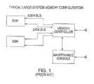
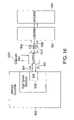
- FIG. 1depicts an example of this early 1980 computer memory subsystem with two BSMs, a memory controller, a maintenance console, and point-to-point address and data busses connecting the BSMs and the memory controller.
- FIG. 2from U.S. Pat. No. 5,513,135 to Dell et al., of common assignment herewith, depicts an early synchronous memory module, which includes synchronous dynamic random access memories (DRAMs) 8 , buffer devices 12 , an optimized pinout, an interconnect and a capacitive decoupling method to facilitate operation.
- DRAMssynchronous dynamic random access memories
- PLLsphase lock loops
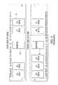
- FIG. 3depicts a simplified diagram and description of a memory system 10 that includes up to four registered dual inline memory modules (DIMMs) 40 on a traditional multi-drop stub bus channel.
- the subsystemincludes a memory controller 20 , an external clock buffer 30 , registered DIMMs 40 , an address bus 50 , a control bus 60 and a data bus 70 with terminators 95 on the address bus 50 and data bus 70 .
- FIG. 4depicts a 1990's memory subsystem which evolved from the structure in FIG. 1 and includes a memory controller 402 , one or more high speed point-to-point channels 404 , each connected to a bus-to-bus converter chip 406 , and each having a synchronous memory interface 408 that enables connection to one or more registered DIMMs 410 .
- the high speed, point-to-point channel 404operated at twice the DRAM data rate, allowing the bus-to-bus converter chip 406 to operate one or two registered DIMM memory channels at the full DRAM data rate.
- Each registered DIMMincluded a PLL, registers, DRAMs, an electrically erasable programmable read-only memory (EEPROM) and terminators, in addition to other passive components.
- EEPROMelectrically erasable programmable read-only memory
- FIG. 5is a simplified example of a multi-drop stub bus memory structure, similar to the one shown in FIG. 3 .
- This structureoffers a reasonable tradeoff between cost, performance, reliability and upgrade capability, but has inherent limits on the number of modules that may be attached to the stub bus.
- the limit on the number of modules that may be attached to the stub busis directly related to the data rate of the information transferred over the bus. As data rates increase, the number and length of the stubs must be reduced to ensure robust memory operation.
- FIG. 6, from U.S. Pat. No. 4,723,120 to Petty, of common assignment herewith,is related to the application of a daisy chain structure in a multipoint communication structure that would otherwise require multiple ports, each connected via point-to-point interfaces to separate devices.
- the controlling stationcan be produced with fewer ports (or channels), and each device on the channel can utilize standard upstream and downstream protocols, independent of their location in the daisy chain structure.
- FIG. 7represents a daisy chained memory bus, implemented consistent with the teachings in U.S. Pat. No. 4,723,120.
- a memory controller 111is connected to a memory bus 315 , which further connects to a module 310 a .
- the information on bus 315is re-driven by the buffer on module 310 a to a next module, 310 b , which further re-drives the bus 315 to module positions denoted as 310 n .
- Each module 310 aincludes a DRAM 311 a and a buffer 320 a .
- the bus 315may be described as having a daisy chain structure with each bus being point-to-point in nature.
- BISTbuilt in self test
- Other known testing solutionsinclude using a built in self test (BIST) mode and/or using a transparent mode.
- BISTis a pre-programmed or programmable sequence and pattern generator, in conjunction with an error checking capability.
- BISTis implemented in many new designs, but it is limited in test coverage and flexibility due to the die size and power. The programmability is limited due to logic complexity. In addition, timing and voltage adjustments are also limited. Therefore, while BIST is often used for testing memory subsystems, it is often supplemented with other testing methods for thorough test coverage.
- Transparent moderefers to the capability of having the automated test equipment (ATE) provide address, command, clocks and data at a conventional speed (e.g., 400 Mb/s data) and the memory module passing the information, unmodified and unchecked, to the DRAMs located on the memory module.
- ATEautomated test equipment
- the use of the transparent mode for testingdoes not result in testing the memory subsystem at full operating speed.
- Exemplary embodiments of the present inventioninclude a buffer device for testing a memory subsystem.
- the buffer deviceincludes a parallel bus port adapted for connection to a slow speed bus and a serial bus port adapted for connection to a high speed bus.
- the high speed busoperates at a faster speed than the slow speed bus.
- the buffer devicealso includes a bus converter having a standard operating mode for converting serial packetized input data received via the serial bus port into parallel bus output data for output via the parallel bus port.
- the buffer devicealso includes an alternate operating mode for converting parallel bus input data received via the parallel bus port into serial packetized output data for output via the serial bus port.
- the serial packetized input datais consistent in function and timing to the serial packetized output data.
- Additional exemplary embodimentsinclude a method for testing a packetized cascade memory subsystem.
- the methodincludes receiving test data at a bus converter.
- the test datais in a parallel bus data format and received via a slow speed bus.
- the test datais converted into a serial packetized data format, resulting in converted test data.
- the converted test datatransmitted to the memory subsystem via a high speed bus.
- the high speed busoperates at a faster speed than the slow speed bus.
- Still further exemplary embodiments of the present inventioninclude a storage medium encoded with machine-readable computer program code for testing a packetized cascade memory subsystem, the storage medium including instructions for causing a computer to implement a method.
- the methodincludes receiving test data at a bus converter.
- the test datais in a parallel bus data format and received via a slow speed bus.
- the test datais converted into a serial packetized data format, resulting in converted test data.
- the converted test datatransmitted to the memory subsystem via a high speed bus.
- the high speed busoperates at a faster speed than the slow speed bus.
- FIG. 1depicts a prior art memory controller connected to two buffered memory assemblies via separate point-to-point links;
- FIG. 2depicts a prior art synchronous memory module with a buffer device
- FIG. 3depicts a prior art memory subsystem using registered DIMMs
- FIG. 4depicts a prior art memory subsystem with point-to-point channels, registered DIMMs, and a 2:1 bus speed multiplier;
- FIG. 5depicts a prior art memory structure that utilizes a multidrop memory ‘stub’ bus
- FIG. 6depicts a prior art daisy chain structure in a multipoint commination structure that would otherwise require multiple ports
- FIG. 7depicts a prior art daisy chain connection between a memory controller and memory modules
- FIG. 8depicts a cascaded memory structure that is utilized by exemplary embodiments of the present invention.
- FIG. 9depicts a memory structure with cascaded memory modules and unidirectional busses that is utilized by exemplary embodiments of the present invention.
- FIG. 10depicts a buffered memory module that is utilized by exemplary embodiments of the present invention.
- FIG. 11depicts a buffered module wiring system that is utilized by exemplary embodiments of the present invention.
- FIG. 12depicts bus and DRAM timing diagrams showing the four to one bus speed multiplier that is utilized by exemplary embodiments of the present invention
- FIG. 13depicts a downstream frame format that is utilized by exemplary embodiments of the present invention.
- FIG. 14depicts a buffer device being utilized to convert slow speed signals from an automated test equipment device into packetized high speed signals for testing a memory subsystem in accordance with exemplary embodiments of the present invention
- FIG. 15depicts buffer devices being utilized to convert slow speed signals from an automated test equipment device into packetized high speed signals and back into slow speed signals for input into the automated test equipment device in accordance with exemplary embodiments of the present invention
- FIG. 16is a block diagram of a board-mounted buffer device that may be tested by exemplary embodiments of the present invention.
- FIG. 17depicts buffer devices being utilized to test unbuffered memory modules in accordance with exemplary embodiments of the present invention.
- Exemplary embodiments of the present inventionutilize the same buffer devices contained in a packetized cascade memory subsystem for testing the packetized cascade memory subsystem.
- a bus converter within the buffer devicereceives serial packetized data (i.e., in a serial bus packetized data input format) from a high speed bus (e.g., 1.6 Gb/s and 3.2 Gb/s) and converts the data into parallel bus data (i.e., in a parallel bus memory data output format) at a slower speed (e.g., 400 Mb/s and 800 Mb/s) for communicating with memory devices (e.g., SDRAMs and DDR 2 s).
- serial packetized datai.e., in a serial bus packetized data input format
- a high speed buse.g., 1.6 Gb/s and 3.2 Gb/s
- parallel bus datai.e., in a parallel bus memory data output format
- a slower speede.g. 400 Mb/s and 800 Mb/s
- the high speed busimplements a packetized multi-transfer interface.
- the bus converter within the buffer deviceconverts slower speed parallel bus data (i.e., in a parallel bus memory data input format) received from testing equipment into serial packetized data (i.e., in a serial bus packetized data output format) for transmission on a high speed bus.
- serial packetized datais used as input for testing the memory subsystem via the high speed bus.
- test datamay be created by standard testing equipment and converted by the buffer device for use in testing a packetized cascade memory subsystem that includes the buffer device and a high speed bus.
- FIG. 8includes a cascaded memory structure that may be tested using a high speed test interface in accordance with exemplary embodiments of the present invention. It includes buffered memory modules 806 (e.g., the buffer device is included within the memory module 806 ) that are in communication with a memory controller 802 .
- This memory structureincludes the memory controller 802 in communication with one or more memory modules 806 via a high speed point-to-point bus 804 .
- Each bus 804 in the exemplary embodiment depicted in FIG. 8includes approximately fifty high speed wires for the transfer of address, command, data and clocks.
- FIG. 4depicts a memory subsystem with a two to one ratio between the data rate on any one of the busses connecting the memory controller to one of the bus converters (e.g., to 1,066 Mb/s per pin) versus any one of the busses between the bus converter and one or more memory modules (e.g., to 533 Mb/s per pin), an exemplary embodiment of the present invention, as depicted in FIG. 8 , provides a four to one bus speed ratio to maximize bus efficiency and to minimize pincount.
- point-to-point interconnectspermit higher data rates, overall memory subsystem efficiency must be achieved by maintaining a reasonable number of memory modules 806 and memory devices per channel (historically four memory modules with four to thirty-six chips per memory module, but as high as eight memory modules per channel and as few as one memory module per channel).
- Using a point-to-point busnecessitates a bus re-drive function on each memory module, to permit memory modules to be cascaded such that each memory module is interconnected to other memory modules, as well as to the memory controller 802 .
- FIG. 9depicts a memory structure with cascaded memory modules and unidirectional busses that may be tested by exemplary embodiments of the present invention.
- One of the functions provided by the memory modules 806 in the cascade structureis a re-drive function to send signals on the memory bus to other memory modules 806 or to the memory controller 802 .
- FIG. 9includes the memory controller 802 and four memory modules 806 a , 806 b , 806 c and 806 d , on each of two memory busses (a downstream memory bus 904 and an upstream memory bus 902 ), connected to the memory controller 802 in either a direct or cascaded manner.
- Memory module 806 ais connected to the memory controller 802 in a direct manner.
- Memory modules 806 b , 806 c and 806 dare connected to the memory controller 802 in a cascaded manner.
- An exemplary memory structureincludes two unidirectional busses between the memory controller 802 and memory module 806 a (“DIMM #1”) as well as between each successive memory module 806 b - d (“DIMM #2”, “DIMM #3” and “DIMM #4”) in the cascaded memory structure.
- the downstream memory bus 904is comprised of twenty-two single-ended signals and a differential clock pair.
- the downstream memory bus 904is used to transfer address, control, write data and bus-level error code correction (ECC) bits downstream from the memory controller 802 , over several clock cycles, to one or more of the memory modules 806 installed on the cascaded memory channel.
- ECCbus-level error code correction
- the upstream memory bus 902is comprised of twenty-three single-ended signals and a differential clock pair, and is used to transfer read data and bus-level ECC bits upstream from the sourcing memory module 806 to the memory controller 802 .
- the memory controller 802 signal pincount, per memory channelis reduced from approximately one hundred and twenty pins to about fifty pins.
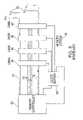
- FIG. 10depicts a front view 1006 and a back view 1008 of the buffered memory module 806 that may be tested by exemplary embodiments of the present invention.
- each memory module 806includes a blank card having dimensions of approximately six inches long by one and a half inches tall, eighteen DRAM positions, a buffer device 1002 , and numerous small components as known in the art that are not shown (e.g., capacitors, resistors, EEPROM.)
- the dimension of the cardis 151.35 mm long by 30.5 mm tall.
- the buffer device 1002is located in the center region of the front side of the memory module 806 , as depicted in the front view 1006 in FIG. 10 .
- Memory devices 1004e.g. synchronous DRAMS (SDRAMS)
- SDRAMSsynchronous DRAMS
- the configurationmay be utilized to facilitate high speed wiring to the buffer device 1002 , as well as signals from the buffer device to the memory devices 1004 .
- FIG. 11depicts a buffered module wiring system that may be tested by utilizing exemplary embodiments of the present invention.
- the buffer device 1002 depicted in FIG. 11running in an alternate operating mode, is utilized as an interface between a testing device and the memory module 806 to perform testing on the memory module 806 in exemplary embodiments of the present invention.
- FIG. 11is a pictorial representation of a memory module, with arrows representing the primary signal flows into and out of the buffer device 1002 during the standard operating mode.
- the signal flowsinclude the upstream memory bus 902 , the downstream memory bus 904 , memory device address and command busses 1102 and 1106 , and memory device data busses 1108 and 1104 .
- the buffer device 1002also referred to as a memory interface chip, provides two copies of the address and command signals to the memory devices 1004 with the right memory device address and command bus 1106 exiting from the right side of the buffer device 1002 for the memory devices 1004 located to the right side and behind the buffer device 1002 on the right.
- a bus converter within the buffer device 1002converts the high speed memory bus data into slower speed address and command signals for communication with the memory devices 1004 .
- the left memory device address and command bus 1102exits from the left side of the buffer device 1002 and connects to the memory devices 1004 to the left side and behind the buffer device 1002 on the left.
- the data bits intended for memory devices 1004 to the right of the buffer device 1002exit from the right of the buffer device 1002 on the right memory device data bus 1108 .
- the data bits intended for the left side of the buffer device 1002exit from the left of the buffer device 1002 on the left memory device data bus 1104 .
- the high speed upstream memory bus 902 and downstream memory bus 904exit from the lower portion of the buffer device 1002 , and connect to a memory controller or other memory modules either upstream or downstream of this memory module 806 , depending on the application.
- the buffer device 1002receives signals that are four times the memory module data rate and converts them into signals at the memory module data rate.
- the memory controller 802interfaces to the memory modules 806 via a pair of high speed busses (or channels).
- the downstream memory bus 904 (outbound from the memory controller 802 ) interfacehas twenty-four pins and the upstream memory bus 902 (inbound to the memory controller 802 ) interface has twenty-five pins.
- the high speed channelseach include a clock pair (differential), a spare bit lane, ECC syndrome bits and the remainder of the bits pass information (based on the operation underway). Due to the cascaded memory structure, all nets are point-to-point, allowing reliable high-speed communication that is independent of the number of memory modules 806 installed. Whenever a memory module 806 receives a packet on either bus, it re-synchronizes the command to the internal clock and re-drives the command to the next memory module 806 in the chain (if one exists).
- FIG. 12depicts bus and SDRAM timing diagrams showing the four to one bus speed multiplier that are utilized by exemplary embodiments of the present invention.
- a bus converter within the buffer device 1002converts high speed serial packetized data into slower speed parallel data.
- the bus converter within the buffer device 1002does the opposite; it converts slower speed parallel data into high speed serial packetized data for use as test data.
- FIG. 12is a simplified “write” timing diagram that demonstrates the bus timing relationships for a write cycle in the preferred embodiment. The same approach may be taken for other cycles, such as a read cycle.
- a high speed bus clock (hsb_clk) 1202is the notation for the positive side of the differential clock that travels with the high speed data traveling downstream from the memory controller 802 to the first memory module 806 , or DIMM. Even though the hsb_clk 1202 is shown as being single-ended, in exemplary embodiments of the present invention, a differential clock is utilized to reduce clock sensitivity to external noise and coupling.
- a high speed data signal (hsb_data) 1204shows a burst of eight transfers, operating at a double data rate speed (i.e., data is valid on both edges of the clock), which in this example constitutes a single frame of address, command and data to the first memory module 806 position.
- a full framecan constitute up to one hundred and seventy-six unique bits, depending on the assignment or use of these bits and the actual wires on the bus.
- This widthis more than adequate to provide the approximately one hundred and twenty memory signals defined as being required by the memory module in FIG. 5 , thereby enabling additional information to be included in the frame to further enhance overall system reliability, fault survivability and/or performance.
- a local memory clock (m_clk) 1208 on the memory module 806is derived from the hsb_clk 1202 , and is shown as a single-ended signal m_clk (0:5) operating at one quarter the frequency of the hsb_clk ( 1202 .
- m_clk 1208would also operate as a differential clock.
- This commandis decoded from the high speed bus and is driven by the buffer to the DDR 2 DRAMS 1004 to ensure arrival at the memory devices 1004 prior to the rising edge of the clock at the memory devices 1004 .
- the seventy-two bits of data written to the DDR 2 memory devices 1004are shown as m_dq(0:71) 1210 , and are shown arriving at the memory devices 1004 one full memory clock after the write command is decoded, as a DDR signal relative to the m_clk 1208 .
- the data, or m_dq(0:71) 1210is single ended.
- the nine DDR data strobes (m_dqs_p) 1212are also shown, as single ended signals, switching one quarter of a clock cycle prior to the DDR 2 SDRAMs 1004 , thereby ensuring that the strobe switches approximately in the center of each valid write data bit.
- the m_dqs_p 1212is differential. This diagram demonstrates a burst of four data bits to the memory devices 1004 (wd 0 through wd 3 ) with seventy-two bits of memory data being provided to the memory devices every memory clock cycle. In this manner, the data rate of the slower memory modules 806 is matched to the high-speed memory bus that operates at four times the speed of the memory modules.
- FIG. 13depicts a downstream frame format that is utilized by exemplary embodiments of the present invention to transfer information downstream from the memory controller 802 to the memory modules 806 .
- the downstream frameconsists of eight transfers with each transfer including twenty-two signals and a differential clock (twenty-four wires total).
- the framefurther consists of eight command wires (c 0 through c 7 ) 1308 , nine data wires (di 0 through di 8 ) 1306 , four bus ECC (Error Correcting Code) wires (ecc 0 through ecc 3 ) 1304 and a spare wire (spare) 1302 .
- the seventy-two data bits referenced in the timing diagram of FIG. 12are shown in FIG.
- bits di 0 through di 8consist of nine wires with eight transfers on each wire for each frame.
- the numbering of each data bit, as well as for other bits,is based on the wire used, as well as the specific transfer.
- D 34refers to data bit 3 (of bits 0 through 8 ) and transfer 4 (of transfer 0 through 7 ).
- the command bit fieldis shown as c 0 through c 7 and consists of sixty-four bits of information provided to the module over eight transfers.
- the ECC bit field(ecc 0 through ecc 3 ) consists of thirty-two bit positions over eight transfers but is actually formatted in groups of sixteen bits. Each sixteen bit packet consists of four transfers over each of the four wires, and provides the bus level fault detection and correction across each group of 4 bus transfers.
- the spare bit positionmay be used to logically replace any of the twenty-one wires, also defined as bitlanes, used to transfer bits in the command, data and ECC fields, should a failure occur in one of those bitlanes that results in errors that exceed a system-assigned failure threshold limit.
- this exemplary embodiment of the present inventionprovides that out of the one hundred and seventy-six possible bit positions, one hundred and sixty-eight are available for the transfer of information to the memory module 806 , and of those one hundred and sixty-eight bit positions, thirty-two bit positions are further assigned to providing ECC protection on the bus transfers themselves, thereby allowing a total of one hundred and thirty-six bit positions to be used for the transfer of information to the memory module 806 .
- Exemplary embodiments of the present inventioninclude the buffer device 1002 described above including an alternate operating mode to be used in testing high speed cascaded memory subsystems, such as those described above, with a slow speed testing device.
- the standard operating mode of the buffer device 1002includes the receipt, ECC correction and bus conversion from a high speed (e.g., 1.6 Gb/s to 3.2 Gb/s) serial packetized bus to a slower (e.g., 400 to 800 Mb/s) parallel DDR 2 memory bus.
- the alternate operating modeincludes having the parallel bus act as the “master” and initiating a bus conversion from the parallel bus to the serial packetized bus when placed in the second operating mode. In the second mode, address, command, clock and data are received on the parallel bus and the buffer device 1002 outputs a properly formatted series of packetized frames which can be used to operate a downstream buffered memory module 806 .
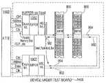
- FIG. 14depicts the buffer device 1002 being utilized to convert slow speed signals from an ATE device 1402 (i.e., a tester device) into packetized high speed signals for testing a memory subsystem in accordance with exemplary embodiments of the present invention.
- FIG. 14depicts the simplest mode of operation, where the buffer device 1002 is placed on an ATE interface board 1406 directly connected to the ATE device 1402 memory interface. In this mode, control signals will be provided to the buffer device 1002 on the control pins (e.g., chip select “CS”, clock enable “CKE”, on die termination “ODT”, column address strobe “CAS”, row address strobe “RAS”, and write enable “WE”).
- address informationwill be provided in conventional RAS/CAS (two cycle transfer) sequence and data will be provided (for write cycles) in a conventional burst of four or eight (programmable) transfers.
- the bus converter device within the buffer device 1002stores and formats the received information, then transmits the information as a high speed eight transfer frame to one or more downstream memory modules 806 .
- the high speed linkcan be operated at 2.1 Gb/s.
- a single memory module 806is shown to the right of the buffer device 1002 as the memory module 806 under test.
- the memory module 806can be fully tested, operating the memory devices 1004 at speed, with and without forced errors.
- other testsmay include retention time testing, temperature testing, voltage testing, and other traditional memory tests that would not otherwise be possible without the parallel to serial bus converter functionality.
- the memory built in self test (BIST) featurescan be fully utilized.
- FIG. 14Also included in FIG. 14 are additional memory modules 806 , connected via dotted lines to the first memory module 806 , indicating the possibility to test multiple memory modules 806 on the same channel. Although intensive real time testing may not be possible on all modules simultaneously, using the BIST modes in conjunction with the conventional test modes, a high degree of parallelism can be obtained.
- FIG. 15depicts buffer devices 1002 being utilized to convert slow speed signals from the ATE device 1402 into packetized high speed signals and back into slow speed signals for input into the ATE device 1402 in accordance with exemplary embodiments of the present invention.
- FIG. 15depicts a test structure that is similar to the one depicted in FIG. 14 with the addition of the buffer device 1002 beyond the last memory module 806 being tested and connected back to the ATE device 1402 .
- This buffer device 1002can be used to receive signals sent downstream from the ATE device 1402 that have passed through the one or more memory modules 806 under test.
- the buffer device 1002can return these signals to the ATE device 1402 in the conventional parallel configuration and either identical in sequence and timings (delayed only by the transfer time downstream from the tester) to the initially transmitted information, or reconfigured, if desired to an alternate configuration.
- the ATE device 1402can send information (typically data and ECC) upstream through the second buffer device 1002 and the upstream memory modules 806 back to the ATE device 1402 to verify both the integrity of the channel, as well as the full functionality of the final memory module 806 in the cascade channel (i.e., the re-drive and receive and data merge function on the high speed channel).
- exemplary embodiments of the present inventionallow an enhanced test capability where the buffer device 1002 may be utilized in a stand alone fashion, upstream from the last memory module 806 under test.
- the buffer device 1002can forward, on its parallel bus, an exact copy of the information initially sent out by the tester, on the tester parallel bus, to the first parallel to serial bus converter device.
- the ATE tester devicewill then be able to compare the information sent out by the tester to the information received by the tester (a pre-defined number of clock counts later) and to determine if any errors have occurred.
- This capabilityprovides a means of performing low cost bit error testing, of inducing bus errors, of verifying bus error detection, and of permitting full testing of the upstream memory port on the memory module 806 under test at full speed.
- commands and data that have been sent out from the ATE device 1402will be sent back to the ATE device 1402 via the second buffer device 1002 to verify the integrity of the memory subsystem.
- a correctable errormay be injected and propagated from the ATE device 1402 to the first buffer device 1002 and converted from low speed to packetized high speed.
- the data with the erroris then sent to the first memory module 806 on the downstream memory bus 904 .
- the erroris then detected at the buffer device 1002 located on the first memory module 806 (e.g., a status condition is set to indicate an error has been detected) and the data is forwarded on to the second memory module 806 .
- the second memory module 806also detects an error and logs a status.
- the data with the errorarrives back at the second buffer device 1002 and is converted from packetized high speed to low speed.
- the ATE device 1402verifies the command that was originally sent out to the first buffer device 1002 .
- FIG. 16is a block diagram of a board-mounted multi-mode buffer device 1002 that may be tested by exemplary embodiments of the present invention.
- FIG. 16demonstrates the use of the multi-mode buffer device 1002 (the same one discussed previously with regard to buffered memory modules 806 ) as a board-mounted bus-to-bus converter chip, attached to one or two unbuffered or registered DIMM memory modules 806 .
- the multi-mode buffer device 1002includes a selection means to adapt the buffer device 1002 for direct attachment to a memory module 806 to enable a buffered memory module mode of operation or to adapt the buffer device 1002 for connection to at least one of an unbuffered memory module and a registered memory module to enable a bus converter mode of operation.
- the selection meansmay be implemented in hardware and/or software.
- a cascade bus 1606is available from the buffer (or exists on the buffer) and can be connected to a buffered DIMM memory module 806 or via another multi-mode buffer device 1002 , to sockets intended for either a second one or two unbuffered or registered DIMM memory modules 806 .
- the memory a (ma) outputs 1604are connected to the first DIMM position and the memory b (mb) outputs 1608 are connected to the second DIMM position, and one or both DIMM positions may be populated based on the application requirements.
- the memory data (md) 1610is connected to both memory modules 806 in FIG. 16 , generally as a conventional multi-drop net.
- An upstream receiver functional block and a downstream driver functional blockare contained in a driver/receiver functional block 1602 within the memory controller 802 .
- An upstream receiver functional block, an upstream driver functional block, a downstream driver functional block and a downstream receiver functional blockare included in the multi-mode buffer device 1002 .
- the upstream memory bus 902 and the downstream memory bus 904are utilized to transfer data, commands, address and clock data between the memory controller 802 and the multi-mode buffer device 1002 .
- FIG. 17depicts buffer devices being utilized to test the board mounted multi-mode buffer device 1002 depicted in FIG. 16 , or alternatively, non-board mounted buffer devices 1002 in accordance with exemplary embodiments of the present invention.
- exemplary embodiments of the present inventionmay be utilized to facilitate early design verification of both buffered memory modules 806 and buffer devices 1002 when used to test unbuffered and/or registered memory modules.
- exemplary embodiments of the present inventionmay be utilized for testing the cascaded memory subsystems described herein.
- the operating modemay be selected via software and/or hardware and memory modules may be shipped with both operating modes or with the alternate operating mode disabled. The alternate operating mode would be enabled for users who perform tests on the memory modules.
- the embodiments of the inventionmay be embodied in the form of computer-implemented processes and apparatuses for practicing those processes.
- Embodiments of the inventionmay also be embodied in the form of computer program code containing instructions embodied in tangible media, such as floppy diskettes, CD-ROMs, hard drives, or any other computer-readable storage medium, wherein, when the computer program code is loaded into and executed by a computer, the computer becomes an apparatus for practicing the invention.
- the present inventioncan also be embodied in the form of computer program code, for example, whether stored in a storage medium, loaded into and/or executed by a computer, or transmitted over some transmission medium, such as over electrical wiring or cabling, through fiber optics, or via electromagnetic radiation, wherein, when the computer program code is loaded into and executed by a computer, the computer becomes an apparatus for practicing the invention.
- computer program code segmentsconfigure the microprocessor to create specific logic circuits.
Landscapes
- Tests Of Electronic Circuits (AREA)
- For Increasing The Reliability Of Semiconductor Memories (AREA)
Abstract
Description
This application is a continuation application of U.S. Ser. No. 10/977,790, filed Oct. 29, 2004, the contents of which are incorporated by reference herein in their entirety.
The invention relates to testing a memory subsystem and in particular, to providing a high speed test interface to a memory subsystem.
Computer memory subsystems have evolved over the years, but continue to retain many consistent attributes. Computer memory subsystems from the early 1980's, such as the one disclosed in U.S. Pat. No. 4,475,194 to LaVallee et al., of common assignment herewith, included a memory controller, a memory assembly (contemporarily called a basic storage module (BSM) by the inventors) with array devices, buffers, terminators and ancillary timing and control functions, as well as several point-to-point busses to permit each memory assembly to communicate with the memory controller via its own point-to-point address and data bus.FIG. 1 depicts an example of this early 1980 computer memory subsystem with two BSMs, a memory controller, a maintenance console, and point-to-point address and data busses connecting the BSMs and the memory controller.
FIG. 2, from U.S. Pat. No. 5,513,135 to Dell et al., of common assignment herewith, depicts an early synchronous memory module, which includes synchronous dynamic random access memories (DRAMs)8,buffer devices 12, an optimized pinout, an interconnect and a capacitive decoupling method to facilitate operation. The patent also describes the use of clock re-drive on the module, using such devices as phase lock loops (PLLs).
FIG. 3, from U.S. Pat. No. 6,510,100 to Grundon et al., of common assignment herewith, depicts a simplified diagram and description of amemory system 10 that includes up to four registered dual inline memory modules (DIMMs)40 on a traditional multi-drop stub bus channel. The subsystem includes amemory controller 20, anexternal clock buffer 30, registeredDIMMs 40, anaddress bus 50, acontrol bus 60 and a data bus70 withterminators 95 on theaddress bus 50 and data bus70.
As shown inFIG. 5 , memory subsystems were often constructed with a memory controller connected either to a single memory module, or to two or more memory modules interconnected on a ‘stub’ bus.FIG. 5 is a simplified example of a multi-drop stub bus memory structure, similar to the one shown inFIG. 3 . This structure offers a reasonable tradeoff between cost, performance, reliability and upgrade capability, but has inherent limits on the number of modules that may be attached to the stub bus. The limit on the number of modules that may be attached to the stub bus is directly related to the data rate of the information transferred over the bus. As data rates increase, the number and length of the stubs must be reduced to ensure robust memory operation. Increasing the speed of the bus generally results in a reduction in modules on the bus, with the optimal electrical interface being one in which a single module is directly connected to a single controller, or a point-to-point interface with few, if any, stubs that will result in reflections and impedance discontinuities. As most memory modules are sixty-four or seventy-two bits in data width, this structure also requires a large number of pins to transfer address, command, and data. One hundred and twenty pins are identified inFIG. 5 as being a representative pincount.
FIG. 6, from U.S. Pat. No. 4,723,120 to Petty, of common assignment herewith, is related to the application of a daisy chain structure in a multipoint communication structure that would otherwise require multiple ports, each connected via point-to-point interfaces to separate devices. By adopting a daisy chain structure, the controlling station can be produced with fewer ports (or channels), and each device on the channel can utilize standard upstream and downstream protocols, independent of their location in the daisy chain structure.
As the density and speed of memory subsystems increases, it becomes more difficult to test memory subsystems with standard test devices. In general, there is a lack of low cost industry test capability for very high speed memory assemblies. Existing mainstream memory device and module testers are capable of operating at data rates of about 200 to 500 megabytes per second (Mb/s) with extensions to 1 gigabyte per second (Gb/s) per pin possible on some test systems, and often at a very high cost. Although higher speed testers are expected in the future, they are not expected to keep pace with rapid performance improvements on future memory modules.
Other known testing solutions include using a built in self test (BIST) mode and/or using a transparent mode. BIST is a pre-programmed or programmable sequence and pattern generator, in conjunction with an error checking capability. BIST is implemented in many new designs, but it is limited in test coverage and flexibility due to the die size and power. The programmability is limited due to logic complexity. In addition, timing and voltage adjustments are also limited. Therefore, while BIST is often used for testing memory subsystems, it is often supplemented with other testing methods for thorough test coverage. Transparent mode refers to the capability of having the automated test equipment (ATE) provide address, command, clocks and data at a conventional speed (e.g., 400 Mb/s data) and the memory module passing the information, unmodified and unchecked, to the DRAMs located on the memory module. The use of the transparent mode for testing does not result in testing the memory subsystem at full operating speed.
Based on the lack of available high speed testers and the limited capability of known test features (e.g., BIST, transparent mode), an alternate method of testing that can be utilized to test high speed devices at a relatively low cost would be useful.
Exemplary embodiments of the present invention include a buffer device for testing a memory subsystem. The buffer device includes a parallel bus port adapted for connection to a slow speed bus and a serial bus port adapted for connection to a high speed bus. The high speed bus operates at a faster speed than the slow speed bus. The buffer device also includes a bus converter having a standard operating mode for converting serial packetized input data received via the serial bus port into parallel bus output data for output via the parallel bus port. The buffer device also includes an alternate operating mode for converting parallel bus input data received via the parallel bus port into serial packetized output data for output via the serial bus port. The serial packetized input data is consistent in function and timing to the serial packetized output data.
Additional exemplary embodiments include a method for testing a packetized cascade memory subsystem. The method includes receiving test data at a bus converter. The test data is in a parallel bus data format and received via a slow speed bus. The test data is converted into a serial packetized data format, resulting in converted test data. The converted test data transmitted to the memory subsystem via a high speed bus. The high speed bus operates at a faster speed than the slow speed bus.
Still further exemplary embodiments of the present invention include a storage medium encoded with machine-readable computer program code for testing a packetized cascade memory subsystem, the storage medium including instructions for causing a computer to implement a method. The method includes receiving test data at a bus converter. The test data is in a parallel bus data format and received via a slow speed bus. The test data is converted into a serial packetized data format, resulting in converted test data. The converted test data transmitted to the memory subsystem via a high speed bus. The high speed bus operates at a faster speed than the slow speed bus.
Referring now to the drawings wherein like elements are numbered alike in the several FIGURES:
Exemplary embodiments of the present invention utilize the same buffer devices contained in a packetized cascade memory subsystem for testing the packetized cascade memory subsystem. When used in the packetized cascade memory subsystem in a standard operating mode, a bus converter within the buffer device receives serial packetized data (i.e., in a serial bus packetized data input format) from a high speed bus (e.g., 1.6 Gb/s and 3.2 Gb/s) and converts the data into parallel bus data (i.e., in a parallel bus memory data output format) at a slower speed (e.g., 400 Mb/s and 800 Mb/s) for communicating with memory devices (e.g., SDRAMs and DDR2s). The high speed bus implements a packetized multi-transfer interface. When used in an alternate operating mode for testing, the bus converter within the buffer device converts slower speed parallel bus data (i.e., in a parallel bus memory data input format) received from testing equipment into serial packetized data (i.e., in a serial bus packetized data output format) for transmission on a high speed bus. The serial packetized data is used as input for testing the memory subsystem via the high speed bus. In this manner, test data may be created by standard testing equipment and converted by the buffer device for use in testing a packetized cascade memory subsystem that includes the buffer device and a high speed bus.
Exemplary embodiments of the present invention provide a high speed test interface to a memory subsystem, such as the one depicted inFIG. 8 .FIG. 8 includes a cascaded memory structure that may be tested using a high speed test interface in accordance with exemplary embodiments of the present invention. It includes buffered memory modules806 (e.g., the buffer device is included within the memory module806) that are in communication with amemory controller 802. This memory structure includes thememory controller 802 in communication with one ormore memory modules 806 via a high speed point-to-point bus 804. Eachbus 804 in the exemplary embodiment depicted inFIG. 8 includes approximately fifty high speed wires for the transfer of address, command, data and clocks. By using point-to-point busses as described in the aforementioned prior art, it is possible to optimize the bus design to permit significantly increased data rates, as well as to reduce the bus pincount by transferring data over multiple cycles. WhereasFIG. 4 depicts a memory subsystem with a two to one ratio between the data rate on any one of the busses connecting the memory controller to one of the bus converters (e.g., to 1,066 Mb/s per pin) versus any one of the busses between the bus converter and one or more memory modules (e.g., to 533 Mb/s per pin), an exemplary embodiment of the present invention, as depicted inFIG. 8 , provides a four to one bus speed ratio to maximize bus efficiency and to minimize pincount.
Although point-to-point interconnects permit higher data rates, overall memory subsystem efficiency must be achieved by maintaining a reasonable number ofmemory modules 806 and memory devices per channel (historically four memory modules with four to thirty-six chips per memory module, but as high as eight memory modules per channel and as few as one memory module per channel). Using a point-to-point bus necessitates a bus re-drive function on each memory module, to permit memory modules to be cascaded such that each memory module is interconnected to other memory modules, as well as to thememory controller 802.
An exemplary memory structure includes two unidirectional busses between thememory controller 802 andmemory module 806a(“DIMM # 1”) as well as between eachsuccessive memory module 806b-d(“DIMM # 2”, “DIMM # 3” and “DIMM # 4”) in the cascaded memory structure. Thedownstream memory bus 904 is comprised of twenty-two single-ended signals and a differential clock pair. Thedownstream memory bus 904 is used to transfer address, control, write data and bus-level error code correction (ECC) bits downstream from thememory controller 802, over several clock cycles, to one or more of thememory modules 806 installed on the cascaded memory channel. Theupstream memory bus 902 is comprised of twenty-three single-ended signals and a differential clock pair, and is used to transfer read data and bus-level ECC bits upstream from thesourcing memory module 806 to thememory controller 802. Using this memory structure, and a four to one data rate multiplier between the DRAM data rate (e.g., slow speed or 400 to 800 Mb/s per pin) and the unidirectional memory bus data rate (e.g., high speed or 1.6 to 3.2 Gb/s per pin), thememory controller 802 signal pincount, per memory channel, is reduced from approximately one hundred and twenty pins to about fifty pins.
Thememory controller 802 interfaces to thememory modules 806 via a pair of high speed busses (or channels). The downstream memory bus904 (outbound from the memory controller802) interface has twenty-four pins and the upstream memory bus902 (inbound to the memory controller802) interface has twenty-five pins. The high speed channels each include a clock pair (differential), a spare bit lane, ECC syndrome bits and the remainder of the bits pass information (based on the operation underway). Due to the cascaded memory structure, all nets are point-to-point, allowing reliable high-speed communication that is independent of the number ofmemory modules 806 installed. Whenever amemory module 806 receives a packet on either bus, it re-synchronizes the command to the internal clock and re-drives the command to thenext memory module 806 in the chain (if one exists).
With the aforementioned downstream bus width of twenty-two bits, and the burst of eight, a full frame can constitute up to one hundred and seventy-six unique bits, depending on the assignment or use of these bits and the actual wires on the bus. This width is more than adequate to provide the approximately one hundred and twenty memory signals defined as being required by the memory module inFIG. 5 , thereby enabling additional information to be included in the frame to further enhance overall system reliability, fault survivability and/or performance.
Also as shown inFIG. 12 , the eight bits occur over four of the hsb_clk cycle times at which point this example shows no further activity on the high speed bus. A local memory clock (m_clk)1208 on thememory module 806 is derived from the hsb_clk1202, and is shown as a single-ended signal m_clk (0:5) operating at one quarter the frequency of the hsb_clk (1202. Although shown as a single-ended clock, in an exemplary embodiment of the present invention, them_clk 1208 would also operate as a differential clock. The decoded memory command signifying a ‘write’ operation to double data rate (DDR2) memory devices, ormemory devices 1004 on thememory module 806, is shown on the signal labeled m_cmd1206. This command is decoded from the high speed bus and is driven by the buffer to theDDR2 DRAMS 1004 to ensure arrival at thememory devices 1004 prior to the rising edge of the clock at thememory devices 1004.
The seventy-two bits of data written to theDDR2 memory devices 1004 are shown as m_dq(0:71)1210, and are shown arriving at thememory devices 1004 one full memory clock after the write command is decoded, as a DDR signal relative to them_clk 1208. In an exemplary embodiment of the present invention, the data, or m_dq(0:71)1210 is single ended. The nine DDR data strobes (m_dqs_p)1212 are also shown, as single ended signals, switching one quarter of a clock cycle prior to theDDR2 SDRAMs 1004, thereby ensuring that the strobe switches approximately in the center of each valid write data bit. In an exemplary embodiment of the present invention, them_dqs_p 1212 is differential. This diagram demonstrates a burst of four data bits to the memory devices1004 (wd0 through wd3) with seventy-two bits of memory data being provided to the memory devices every memory clock cycle. In this manner, the data rate of theslower memory modules 806 is matched to the high-speed memory bus that operates at four times the speed of the memory modules.
The command bit field is shown as c0 through c7 and consists of sixty-four bits of information provided to the module over eight transfers. The ECC bit field (ecc0 through ecc3) consists of thirty-two bit positions over eight transfers but is actually formatted in groups of sixteen bits. Each sixteen bit packet consists of four transfers over each of the four wires, and provides the bus level fault detection and correction across each group of 4 bus transfers. The spare bit position may be used to logically replace any of the twenty-one wires, also defined as bitlanes, used to transfer bits in the command, data and ECC fields, should a failure occur in one of those bitlanes that results in errors that exceed a system-assigned failure threshold limit. Using this exemplary embodiment of the present invention provides that out of the one hundred and seventy-six possible bit positions, one hundred and sixty-eight are available for the transfer of information to thememory module 806, and of those one hundred and sixty-eight bit positions, thirty-two bit positions are further assigned to providing ECC protection on the bus transfers themselves, thereby allowing a total of one hundred and thirty-six bit positions to be used for the transfer of information to thememory module 806.
Exemplary embodiments of the present invention include thebuffer device 1002 described above including an alternate operating mode to be used in testing high speed cascaded memory subsystems, such as those described above, with a slow speed testing device. As described above, the standard operating mode of thebuffer device 1002 includes the receipt, ECC correction and bus conversion from a high speed (e.g., 1.6 Gb/s to 3.2 Gb/s) serial packetized bus to a slower (e.g., 400 to 800 Mb/s) parallel DDR2 memory bus. The alternate operating mode includes having the parallel bus act as the “master” and initiating a bus conversion from the parallel bus to the serial packetized bus when placed in the second operating mode. In the second mode, address, command, clock and data are received on the parallel bus and thebuffer device 1002 outputs a properly formatted series of packetized frames which can be used to operate a downstream bufferedmemory module 806.
InFIG. 14 , asingle memory module 806 is shown to the right of thebuffer device 1002 as thememory module 806 under test. In this example, only the upstream side of thememory module 806 is fully tested. Thememory module 806 can be fully tested, operating thememory devices 1004 at speed, with and without forced errors. In exemplary embodiments of the present invention other tests may include retention time testing, temperature testing, voltage testing, and other traditional memory tests that would not otherwise be possible without the parallel to serial bus converter functionality. In addition to traditional testing, the memory built in self test (BIST) features can be fully utilized.
Also included inFIG. 14 areadditional memory modules 806, connected via dotted lines to thefirst memory module 806, indicating the possibility to testmultiple memory modules 806 on the same channel. Although intensive real time testing may not be possible on all modules simultaneously, using the BIST modes in conjunction with the conventional test modes, a high degree of parallelism can be obtained.
In addition to using the standard and alternate operating modes in thebuffer device 1002 for testing, exemplary embodiments of the present invention allow an enhanced test capability where thebuffer device 1002 may be utilized in a stand alone fashion, upstream from thelast memory module 806 under test. Thebuffer device 1002 can forward, on its parallel bus, an exact copy of the information initially sent out by the tester, on the tester parallel bus, to the first parallel to serial bus converter device. The ATE tester device will then be able to compare the information sent out by the tester to the information received by the tester (a pre-defined number of clock counts later) and to determine if any errors have occurred. This capability provides a means of performing low cost bit error testing, of inducing bus errors, of verifying bus error detection, and of permitting full testing of the upstream memory port on thememory module 806 under test at full speed.
In an exemplary embodiment of the present invention, commands and data that have been sent out from the ATEdevice 1402 will be sent back to the ATEdevice 1402 via thesecond buffer device 1002 to verify the integrity of the memory subsystem. For example, a correctable error may be injected and propagated from the ATEdevice 1402 to thefirst buffer device 1002 and converted from low speed to packetized high speed. The data with the error is then sent to thefirst memory module 806 on thedownstream memory bus 904. The error is then detected at thebuffer device 1002 located on the first memory module806 (e.g., a status condition is set to indicate an error has been detected) and the data is forwarded on to thesecond memory module 806. Thesecond memory module 806 also detects an error and logs a status. Eventually, the data with the error arrives back at thesecond buffer device 1002 and is converted from packetized high speed to low speed. The ATEdevice 1402 then verifies the command that was originally sent out to thefirst buffer device 1002.
By implementing the logic associated with standard and alternate operating modes of thebuffer device 1002 described herein, it is possible to utilize existing ATE devices to fully testmemory modules 806, at speed and at a low cost. This capability further reduces the added cost of having a different high speed interface because thebuffer devices 1002 with high speed interfaces can be utilized for their own testing. In addition, exemplary embodiments of the present invention may be utilized for testing the cascaded memory subsystems described herein. The operating mode may be selected via software and/or hardware and memory modules may be shipped with both operating modes or with the alternate operating mode disabled. The alternate operating mode would be enabled for users who perform tests on the memory modules.
As described above, the embodiments of the invention may be embodied in the form of computer-implemented processes and apparatuses for practicing those processes. Embodiments of the invention may also be embodied in the form of computer program code containing instructions embodied in tangible media, such as floppy diskettes, CD-ROMs, hard drives, or any other computer-readable storage medium, wherein, when the computer program code is loaded into and executed by a computer, the computer becomes an apparatus for practicing the invention. The present invention can also be embodied in the form of computer program code, for example, whether stored in a storage medium, loaded into and/or executed by a computer, or transmitted over some transmission medium, such as over electrical wiring or cabling, through fiber optics, or via electromagnetic radiation, wherein, when the computer program code is loaded into and executed by a computer, the computer becomes an apparatus for practicing the invention. When implemented on a general-purpose microprocessor, the computer program code segments configure the microprocessor to create specific logic circuits.
While the invention has been described with reference to exemplary embodiments, it will be understood by those skilled in the art that various changes may be made and equivalents may be substituted for elements thereof without departing from the scope of the invention. In addition, many modifications may be made to adapt a particular situation or material to the teachings of the invention without departing from the essential scope thereof. Therefore, it is intended that the invention not be limited to the particular embodiment disclosed as the best mode contemplated for carrying out this invention, but that the invention will include all embodiments falling within the scope of the appended claims. Moreover, the use of the terms first, second, etc. do not denote any order or importance, but rather the terms first, second, etc. are used to distinguish one element from another.
Claims (19)
1. A buffer device for testing a memory subsystem, the buffer device comprising:
a parallel bus port adapted for connection to a slow speed bus;
a serial bus port adapted for connection to a high speed bus, wherein the high speed bus operates at a faster speed than the slow speed bus; and
a bus converter having a standard operating mode for converting serial packetized input data received via the serial bus port into parallel bus output data for output via the parallel bus port and an alternate operating mode for converting parallel bus input data received via the parallel bus port into serial packetized output data for output via the serial bus port, wherein the serial packetized input data is consistent in function and timing to the serial packetized output data.
2. The buffer device ofclaim 1 wherein the high speed bus operates at four times the speed of the slow speed bus.
3. The buffer device ofclaim 1 wherein the slow speed bus operates at a dynamic random access memory (DRAM) data rate.
4. The buffer device ofclaim 1 wherein the serial packetized output data output via the serial bus port emulates a high speed bus.
5. The buffer device ofclaim 1 wherein the serial packetized output data for output via the serial bus port emulates a high speed interface for communicating to a buffered memory module.
6. A system comprising:
a buffer device comprising:
a parallel bus port adapted for connection to a slow speed bus;
a serial bus port adapted for connection to a high speed bus, wherein the high speed bus operates at a faster speed than the slow speed bus; and
a bus converter having a standard operating mode for converting serial packetized input data received via the serial bus port into parallel bus output data for output via the parallel bus port and an alternate operating mode for converting parallel bus input data received via the parallel bus port into serial packetized output data for output via the serial bus port, wherein the serial packetized input data is consistent in function and timing to the serial packetized output data; and
a tester device adapted for connection to the slow speed bus and including instructions for creating test data and for transmitting the test data as parallel bus input test data to the parallel bus port via the slow speed bus.
7. The system ofclaim 6 wherein the tester device includes further instructions for receiving test result data responsive to the test data from the buffer device, the receiving via the slow speed bus.
8. A system comprising:
a buffer device comprising:
a parallel bus port adapted for connection to a slow speed bus;
a serial bus port adapted for connection to a high speed bus, wherein the high speed bus operates at a faster speed than the slow speed bus; and
a bus converter having a standard operating mode for converting serial packetized input data received via the serial bus port into parallel bus output data for output via the parallel bus port and an alternate operating mode for converting parallel bus input data received via the parallel bus port into serial packetized output data for output via the serial bus port, wherein the serial packetized input data is consistent in function and timing to the serial packetized output data; and
a buffered memory module adapted for connection to the high speed bus and including instructions for receiving test data as serial packetized output test data from the serial bus port via the high speed bus.
9. The system ofclaim 8 wherein the buffered memory module includes further instructions for transmitting test result data responsive to the test data to the serial bus port via the high speed bus.
10. The system ofclaim 8 wherein the buffered memory module includes a memory device and a second bus converter operating in the standard mode for receiving the test data as serial packetized data and for converting the test data into parallel bus data for communication with the memory device.
11. The system ofclaim 8 wherein the buffered memory module is adapted to be connected to a packetized cascade memory subsystem via a packetized multi-transfer interface.
12. The system ofclaim 8 wherein the buffered memory module is adapted to be connected to one or more unbuffered memory modules and registered memory modules.
13. The system ofclaim 12 wherein the buffered memory module and the one or more unbuffered memory modules and registered memory modules are board mounted.
14. A storage medium encoded with machine-readable computer program code for testing a packetized cascade memory subsystem, the storage medium including instructions for causing a computer to implement a method comprising:
receiving test data at a bus converter, the test data in a parallel bus data format and received via a slow speed bus;
converting the test data into a serial packetized data format resulting in converted test data; and
transmitting the converted test data to the memory subsystem via a high speed bus, wherein the high speed bus operates at a faster speed than the slow speed bus.
15. The storage medium ofclaim 14 wherein the high speed bus operates at four times the speed of the slow speed bus.
16. The storage medium ofclaim 14 wherein the test data is received from a tester device operating at the same speed as the slow speed bus.
17. The storage medium ofclaim 14 wherein the high speed bus operates at the same speed as the memory subsystem.
18. The storage medium ofclaim 14 further comprising:
receiving test result data from the memory subsystem via the high speed bus, wherein the test result data is responsive to the test data and is in the serial packetized data format;
converting the test result data into the parallel bus data format resulting in converted test result data; and
transmitting the converted test result data to a tester device via the slow speed bus.
19. The storage medium ofclaim 14 wherein the memory subsystem includes a memory device operating at the speed of the slow speed bus and an other bus converter for receiving the converted test data and for converting the test data into the parallel bus data input format for communication with the memory device.
Priority Applications (1)
| Application Number | Priority Date | Filing Date | Title |
|---|---|---|---|
| US11/971,578US7475316B2 (en) | 2004-10-29 | 2008-01-09 | System, method and storage medium for providing a high speed test interface to a memory subsystem |
Applications Claiming Priority (2)
| Application Number | Priority Date | Filing Date | Title |
|---|---|---|---|
| US10/977,790US7395476B2 (en) | 2004-10-29 | 2004-10-29 | System, method and storage medium for providing a high speed test interface to a memory subsystem |
| US11/971,578US7475316B2 (en) | 2004-10-29 | 2008-01-09 | System, method and storage medium for providing a high speed test interface to a memory subsystem |
Related Parent Applications (1)
| Application Number | Title | Priority Date | Filing Date |
|---|---|---|---|
| US10/977,790ContinuationUS7395476B2 (en) | 2004-10-29 | 2004-10-29 | System, method and storage medium for providing a high speed test interface to a memory subsystem |
Publications (2)
| Publication Number | Publication Date |
|---|---|
| US20080104290A1 US20080104290A1 (en) | 2008-05-01 |
| US7475316B2true US7475316B2 (en) | 2009-01-06 |
Family
ID=36387914
Family Applications (2)
| Application Number | Title | Priority Date | Filing Date |
|---|---|---|---|
| US10/977,790Expired - LifetimeUS7395476B2 (en) | 2004-10-29 | 2004-10-29 | System, method and storage medium for providing a high speed test interface to a memory subsystem |
| US11/971,578Expired - LifetimeUS7475316B2 (en) | 2004-10-29 | 2008-01-09 | System, method and storage medium for providing a high speed test interface to a memory subsystem |
Family Applications Before (1)
| Application Number | Title | Priority Date | Filing Date |
|---|---|---|---|
| US10/977,790Expired - LifetimeUS7395476B2 (en) | 2004-10-29 | 2004-10-29 | System, method and storage medium for providing a high speed test interface to a memory subsystem |
Country Status (1)
| Country | Link |
|---|---|
| US (2) | US7395476B2 (en) |
Cited By (12)
| Publication number | Priority date | Publication date | Assignee | Title |
|---|---|---|---|---|
| US20080115022A1 (en)* | 2006-10-19 | 2008-05-15 | Chun-Yuan Su | System and related method for chip i/o test |
| US20080266993A1 (en)* | 2007-04-25 | 2008-10-30 | Martin Goldsteln | Serial connection external interface from printed circuit board translation to parallel memory protocol |
| US20090021404A1 (en)* | 2007-07-20 | 2009-01-22 | Micron Technology, Inc. | Variable resistance logic |
| US20090217235A1 (en)* | 2008-02-27 | 2009-08-27 | Sap Ag | Apparatus and Method of Generating Self-Debugging Computer Software |
| US20090316510A1 (en)* | 2008-06-23 | 2009-12-24 | Elpida Memory, Inc. | Semiconductor device and data processing system |
| US7711887B1 (en)* | 2007-04-30 | 2010-05-04 | Hewlett-Packard Development Company, L.P. | Employing a native fully buffered dual in-line memory module protocol to write parallel protocol memory module channels |
| US7739441B1 (en)* | 2007-04-30 | 2010-06-15 | Hewlett-Packard Development Company, L.P. | Communicating between a native fully buffered dual in-line memory module protocol and a double data rate synchronous dynamic random access memory protocol |
| US7996602B1 (en) | 2007-04-30 | 2011-08-09 | Hewlett-Packard Development Company, L.P. | Parallel memory device rank selection |
| US8102671B2 (en) | 2007-04-25 | 2012-01-24 | Hewlett-Packard Development Company, L.P. | Serial connection external interface riser cards avoidance of abutment of parallel connection external interface memory modules |
| US9405339B1 (en) | 2007-04-30 | 2016-08-02 | Hewlett Packard Enterprise Development Lp | Power controller |
| US9811266B1 (en)* | 2016-09-22 | 2017-11-07 | Cisco Technology, Inc. | Data buffer for multiple DIMM topology |
| US10388396B2 (en) | 2014-08-25 | 2019-08-20 | Rambus Inc. | Buffer circuit with adaptive repair capability |
Families Citing this family (79)
| Publication number | Priority date | Publication date | Assignee | Title |
|---|---|---|---|---|
| US7365557B1 (en) | 2001-09-28 | 2008-04-29 | Inapac Technology, Inc. | Integrated circuit testing module including data generator |
| US8166361B2 (en)* | 2001-09-28 | 2012-04-24 | Rambus Inc. | Integrated circuit testing module configured for set-up and hold time testing |
| US7265570B2 (en)* | 2001-09-28 | 2007-09-04 | Inapac Technology, Inc. | Integrated circuit testing module |
| US7370256B2 (en)* | 2001-09-28 | 2008-05-06 | Inapac Technology, Inc. | Integrated circuit testing module including data compression |
| US8286046B2 (en) | 2001-09-28 | 2012-10-09 | Rambus Inc. | Integrated circuit testing module including signal shaping interface |
| US8001439B2 (en) | 2001-09-28 | 2011-08-16 | Rambus Inc. | Integrated circuit testing module including signal shaping interface |
| US7446551B1 (en) | 2001-09-28 | 2008-11-04 | Inapac Technology, Inc. | Integrated circuit testing module including address generator |
| US8060799B2 (en)* | 2004-06-11 | 2011-11-15 | Samsung Electronics Co., Ltd. | Hub, memory module, memory system and methods for reading and writing to the same |
| DE102004056214B4 (en)* | 2004-11-22 | 2006-12-14 | Infineon Technologies Ag | memory buffer |
| US7328381B2 (en)* | 2005-08-01 | 2008-02-05 | Micron Technology, Inc. | Testing system and method for memory modules having a memory hub architecture |
| US7319340B2 (en)* | 2005-08-01 | 2008-01-15 | Micron Technology, Inc. | Integrated circuit load board and method having on-board test circuit |
| US7765424B2 (en)* | 2005-08-19 | 2010-07-27 | Micron Technology, Inc. | System and method for injecting phase jitter into integrated circuit test signals |
| US7475187B2 (en)* | 2005-09-15 | 2009-01-06 | Infineon Technologies Ag | High-speed interface circuit for semiconductor memory chips and memory system including the same |
| US7779311B2 (en)* | 2005-10-24 | 2010-08-17 | Rambus Inc. | Testing and recovery in a multilayer device |
| US7355387B2 (en)* | 2005-12-08 | 2008-04-08 | Micron Technology, Inc. | System and method for testing integrated circuit timing margins |
| US7284169B2 (en)* | 2005-12-08 | 2007-10-16 | Micron Technology, Inc. | System and method for testing write strobe timing margins in memory devices |
| US7561027B2 (en)* | 2006-10-26 | 2009-07-14 | Hewlett-Packard Development Company, L.P. | Sensing device |
| KR100825791B1 (en)* | 2006-11-08 | 2008-04-29 | 삼성전자주식회사 | High speed memory device that can be easily tested using low speed ATE equipment and input / output pin control method therefor |
| US7508724B2 (en)* | 2006-11-30 | 2009-03-24 | Mosaid Technologies Incorporated | Circuit and method for testing multi-device systems |
| TWI306951B (en)* | 2006-12-19 | 2009-03-01 | Via Tech Inc | Chipset and chipset testing method |
| WO2008079911A1 (en)* | 2006-12-21 | 2008-07-03 | Rambus Inc. | Dynamic on-die termination of address and command signals |
| US20080235542A1 (en)* | 2007-03-22 | 2008-09-25 | Duncan Gurley | Electronic testing device for memory devices and related methods |
| US7707468B2 (en)* | 2007-03-22 | 2010-04-27 | Verigy (Singapore) Pte. Ltd | System and method for electronic testing of multiple memory devices |
| US7739562B2 (en) | 2007-08-17 | 2010-06-15 | International Business Machines Corporation | Programmable diagnostic memory module |
| US7730369B2 (en)* | 2007-08-17 | 2010-06-01 | International Business Machines Corporation | Method for performing memory diagnostics using a programmable diagnostic memory module |
| US8384410B1 (en) | 2007-08-24 | 2013-02-26 | Advantest (Singapore) Pte Ltd | Parallel test circuit with active devices |
| US7827452B2 (en)* | 2007-08-24 | 2010-11-02 | Verigy (Singapore) Pte. Ltd. | Error catch RAM support using fan-out/fan-in matrix |
| US7913128B2 (en)* | 2007-11-23 | 2011-03-22 | Mosaid Technologies Incorporated | Data channel test apparatus and method thereof |
| US8242796B2 (en)* | 2008-02-21 | 2012-08-14 | Advantest (Singapore) Pte Ltd | Transmit/receive unit, and methods and apparatus for transmitting signals between transmit/receive units |
| US7928755B2 (en)* | 2008-02-21 | 2011-04-19 | Verigy (Singapore) Pte. Ltd. | Methods and apparatus that selectively use or bypass a remote pin electronics block to test at least one device under test |
| US8516185B2 (en) | 2009-07-16 | 2013-08-20 | Netlist, Inc. | System and method utilizing distributed byte-wise buffers on a memory module |
| US7717752B2 (en)* | 2008-07-01 | 2010-05-18 | International Business Machines Corporation | 276-pin buffered memory module with enhanced memory system interconnect and features |
| US20100005212A1 (en)* | 2008-07-01 | 2010-01-07 | International Business Machines Corporation | Providing a variable frame format protocol in a cascade interconnected memory system |
| US20100005219A1 (en)* | 2008-07-01 | 2010-01-07 | International Business Machines Corporation | 276-pin buffered memory module with enhanced memory system interconnect and features |
| US20100005218A1 (en)* | 2008-07-01 | 2010-01-07 | International Business Machines Corporation | Enhanced cascade interconnected memory system |
| US20100005220A1 (en)* | 2008-07-01 | 2010-01-07 | International Business Machines Corporation | 276-pin buffered memory module with enhanced memory system interconnect and features |
| US20100005214A1 (en)* | 2008-07-01 | 2010-01-07 | International Business Machines Corporation | Enhancing bus efficiency in a memory system |
| US20100005206A1 (en)* | 2008-07-01 | 2010-01-07 | International Business Machines Corporation | Automatic read data flow control in a cascade interconnect memory system |
| US9047987B2 (en)* | 2008-07-22 | 2015-06-02 | International Microsystems, Inc. | Multiple access test architecture for memory storage devices |
| US8085685B2 (en)* | 2009-09-21 | 2011-12-27 | Litepoint Corporation | Method and system for testing multiple data packet transceivers together during a predetermined time interval |
| US8116208B2 (en)* | 2009-10-19 | 2012-02-14 | Litepoint Corporation | System and method for testing multiple digital signal transceivers in parallel |
| US8316175B2 (en) | 2009-11-03 | 2012-11-20 | Inphi Corporation | High throughput flash memory system |
| KR101215973B1 (en)* | 2010-12-30 | 2012-12-27 | 에스케이하이닉스 주식회사 | Integrated circuit, system including the same, memory and memory system |
| US9170878B2 (en) | 2011-04-11 | 2015-10-27 | Inphi Corporation | Memory buffer with data scrambling and error correction |
| US8880790B2 (en)* | 2011-04-11 | 2014-11-04 | Inphi Corporation | Methods and apparatus for transferring data between memory modules |
| TWI473107B (en)* | 2011-05-24 | 2015-02-11 | Powertech Technology Inc | Test interface board enabling to programmably speed testing signal |
| US8687451B2 (en) | 2011-07-26 | 2014-04-01 | Inphi Corporation | Power management in semiconductor memory system |
| US9158726B2 (en) | 2011-12-16 | 2015-10-13 | Inphi Corporation | Self terminated dynamic random access memory |
| US20150058524A1 (en)* | 2012-01-04 | 2015-02-26 | Kenneth C. Creta | Bimodal functionality between coherent link and memory expansion |
| US8949473B1 (en) | 2012-02-16 | 2015-02-03 | Inphi Corporation | Hybrid memory blade |
| US9230635B1 (en) | 2012-03-06 | 2016-01-05 | Inphi Corporation | Memory parametric improvements |
| US8861277B1 (en) | 2012-06-26 | 2014-10-14 | Inphi Corporation | Method of using non-volatile memories for on-DIMM memory address list storage |
| US9026870B2 (en)* | 2012-07-27 | 2015-05-05 | Samsung Electronics Co., Ltd. | Memory module and a memory test system for testing the same |
| US9647799B2 (en) | 2012-10-16 | 2017-05-09 | Inphi Corporation | FEC coding identification |
| US10185499B1 (en) | 2014-01-07 | 2019-01-22 | Rambus Inc. | Near-memory compute module |
| US9553670B2 (en) | 2014-03-03 | 2017-01-24 | Inphi Corporation | Optical module |
| US20150255176A1 (en)* | 2014-03-10 | 2015-09-10 | Advantest Corporation | Memory test ecc auto-correction of failing data |
| US9792965B2 (en)* | 2014-06-17 | 2017-10-17 | Rambus Inc. | Memory module and system supporting parallel and serial access modes |
| US9874800B2 (en) | 2014-08-28 | 2018-01-23 | Inphi Corporation | MZM linear driver for silicon photonics device characterized as two-channel wavelength combiner and locker |
| US9325419B1 (en) | 2014-11-07 | 2016-04-26 | Inphi Corporation | Wavelength control of two-channel DEMUX/MUX in silicon photonics |
| US9473090B2 (en) | 2014-11-21 | 2016-10-18 | Inphi Corporation | Trans-impedance amplifier with replica gain control |
| US9553689B2 (en) | 2014-12-12 | 2017-01-24 | Inphi Corporation | Temperature insensitive DEMUX/MUX in silicon photonics |
| US9461677B1 (en) | 2015-01-08 | 2016-10-04 | Inphi Corporation | Local phase correction |
| US9484960B1 (en) | 2015-01-21 | 2016-11-01 | Inphi Corporation | Reconfigurable FEC |
| US9547129B1 (en) | 2015-01-21 | 2017-01-17 | Inphi Corporation | Fiber coupler for silicon photonics |
| US9548726B1 (en) | 2015-02-13 | 2017-01-17 | Inphi Corporation | Slew-rate control and waveshape adjusted drivers for improving signal integrity on multi-loads transmission line interconnects |
| US9632390B1 (en) | 2015-03-06 | 2017-04-25 | Inphi Corporation | Balanced Mach-Zehnder modulator |
| US9842038B2 (en) | 2015-04-30 | 2017-12-12 | Advantest Corporation | Method and system for advanced fail data transfer mechanisms |
| US10169258B2 (en)* | 2015-06-09 | 2019-01-01 | Rambus Inc. | Memory system design using buffer(s) on a mother board |
| US9847839B2 (en) | 2016-03-04 | 2017-12-19 | Inphi Corporation | PAM4 transceivers for high-speed communication |
| KR20180002939A (en)* | 2016-06-29 | 2018-01-09 | 삼성전자주식회사 | Memory device, memory package including the same, and memory module including the same |
| CN106887257B (en)* | 2017-03-16 | 2020-12-04 | 数据通信科学技术研究所 | Multi-smart-card testing system and method |
| US10572427B2 (en) | 2017-11-13 | 2020-02-25 | Data I/O Corporation | Device programming system with protocol emulation |
| KR20210131392A (en)* | 2019-02-22 | 2021-11-02 | 마이크론 테크놀로지, 인크. | Memory device interfaces and methods |
| US11048439B2 (en)* | 2019-06-21 | 2021-06-29 | Eorex Corporation | Device of memory modules |
| EP4081954A4 (en) | 2019-12-27 | 2023-04-05 | Micron Technology, Inc. | Neuromorphic memory device and method |
| US11635910B2 (en) | 2019-12-30 | 2023-04-25 | Micron Technology, Inc. | Memory device interface and method |
| WO2021138408A1 (en) | 2019-12-31 | 2021-07-08 | Micron Technology, Inc. | Memory module mutiple port buffer techniques |
| CN113035267B (en)* | 2021-03-25 | 2022-05-13 | 长江存储科技有限责任公司 | A semiconductor testing device, data processing method, equipment and storage medium |
Citations (239)
| Publication number | Priority date | Publication date | Assignee | Title |
|---|---|---|---|---|
| US2842682A (en) | 1956-09-04 | 1958-07-08 | Ibm | Reversible shift register |
| US3333253A (en) | 1965-02-01 | 1967-07-25 | Ibm | Serial-to-parallel and parallel-toserial buffer-converter using a core matrix |
| US3395400A (en) | 1966-04-26 | 1968-07-30 | Bell Telephone Labor Inc | Serial to parallel data converter |
| US3825904A (en) | 1973-06-08 | 1974-07-23 | Ibm | Virtual memory system |
| US4028675A (en) | 1973-05-14 | 1977-06-07 | Hewlett-Packard Company | Method and apparatus for refreshing semiconductor memories in multi-port and multi-module memory system |
| US4135240A (en) | 1973-07-09 | 1979-01-16 | Bell Telephone Laboratories, Incorporated | Protection of data file contents |
| JPS59153353A (en) | 1983-02-22 | 1984-09-01 | Nec Corp | Data transmission system |
| US4472780A (en) | 1981-09-28 | 1984-09-18 | The Boeing Company | Fly-by-wire lateral control system |
| US4475194A (en) | 1982-03-30 | 1984-10-02 | International Business Machines Corporation | Dynamic replacement of defective memory words |
| US4486739A (en) | 1982-06-30 | 1984-12-04 | International Business Machines Corporation | Byte oriented DC balanced (0,4) 8B/10B partitioned block transmission code |
| US4641263A (en) | 1982-05-17 | 1987-02-03 | Digital Associates Corporation | Controller system or emulating local parallel minicomputer/printer interface and transferring serial data to remote line printer |
| US4654857A (en) | 1981-10-01 | 1987-03-31 | Stratus Computer, Inc. | Digital data processor with high reliability |
| US4723120A (en) | 1986-01-14 | 1988-02-02 | International Business Machines Corporation | Method and apparatus for constructing and operating multipoint communication networks utilizing point-to point hardware and interfaces |
| US4740916A (en) | 1985-12-19 | 1988-04-26 | International Business Machines Corporation | Reconfigurable contiguous address space memory system including serially connected variable capacity memory modules and a split address bus |
| US4796231A (en) | 1985-01-22 | 1989-01-03 | Texas Instruments Incorporated | Serial accessed semiconductor memory with reconfigurable shift registers |
| US4803485A (en) | 1987-03-23 | 1989-02-07 | Amp Incorporated | Lan communication system and medium adapter for use therewith |
| US4833605A (en) | 1984-08-16 | 1989-05-23 | Mitsubishi Denki Kabushiki Kaisha | Cascaded information processing module having operation unit, parallel port, and serial port for concurrent data transfer and data processing |
| US4839534A (en) | 1986-10-16 | 1989-06-13 | Siemens Aktiengesellschaft | Method and apparatus for establishing a system clock in response to the level of one of two clock signal sources |
| US4943984A (en) | 1988-06-24 | 1990-07-24 | International Business Machines Corporation | Data processing system parallel data bus having a single oscillator clocking apparatus |
| US4985828A (en) | 1987-03-19 | 1991-01-15 | Hitachi, Ltd. | Method and apparatus for generating a real address multiple virtual address spaces of a storage |
| US5053947A (en) | 1989-09-29 | 1991-10-01 | Allegro Microsystems, Inc. | Extended multistation bus system and method |
| EP0470734A1 (en) | 1990-08-06 | 1992-02-12 | NCR International, Inc. | Cache memory management system |
| US5177375A (en) | 1989-12-28 | 1993-01-05 | Mitsubishi Denki Kabushiki Kaisha | Power on reset circuit for semiconductor integrated circuit device |
| US5206946A (en) | 1989-10-27 | 1993-04-27 | Sand Technology Systems Development, Inc. | Apparatus using converters, multiplexer and two latches to convert SCSI data into serial data and vice versa |
| US5214747A (en) | 1990-12-24 | 1993-05-25 | Eastman Kodak Company | Segmented neural network with daisy chain control |
| US5265212A (en) | 1992-04-01 | 1993-11-23 | Digital Equipment Corporation | Sharing of bus access among multiple state machines with minimal wait time and prioritization of like cycle types |
| US5287531A (en) | 1990-10-31 | 1994-02-15 | Compaq Computer Corp. | Daisy-chained serial shift register for determining configuration of removable circuit boards in a computer system |
| US5347270A (en) | 1991-12-27 | 1994-09-13 | Mitsubishi Denki Kabushiki Kaisha | Method of testing switches and switching circuit |
| US5357621A (en) | 1990-09-04 | 1994-10-18 | Hewlett-Packard Company | Serial architecture for memory module control |
| US5375127A (en) | 1992-03-25 | 1994-12-20 | Ncr Corporation | Method and apparatus for generating Reed-Soloman error correcting code across multiple word boundaries |
| US5387911A (en) | 1992-02-21 | 1995-02-07 | Gleichert; Marc C. | Method and apparatus for transmitting and receiving both 8B/10B code and 10B/12B code in a switchable 8B/10B transmitter and receiver |
| US5394535A (en) | 1989-04-21 | 1995-02-28 | Nec Corporation | Memory access control circuit with automatic access mode determination circuitry with read-modify-write and write-per-bit operations |
| US5454091A (en) | 1990-06-29 | 1995-09-26 | Digital Equipment Corporation | Virtual to physical address translation scheme with granularity hint for identifying subsequent pages to be accessed |
| US5475690A (en) | 1994-11-10 | 1995-12-12 | Digital Equipment Corporation | Delay compensated signal propagation |
| US5513135A (en) | 1994-12-02 | 1996-04-30 | International Business Machines Corporation | Synchronous memory packaged in single/dual in-line memory module and method of fabrication |
| US5517626A (en) | 1990-05-07 | 1996-05-14 | S3, Incorporated | Open high speed bus for microcomputer system |
| US5522064A (en) | 1990-10-01 | 1996-05-28 | International Business Machines Corporation | Data processing apparatus for dynamically setting timings in a dynamic memory system |
| US5544309A (en) | 1993-04-22 | 1996-08-06 | International Business Machines Corporation | Data processing system with modified planar for boundary scan diagnostics |
| US5546023A (en) | 1995-06-26 | 1996-08-13 | Intel Corporation | Daisy chained clock distribution scheme |
| US5561826A (en) | 1990-05-25 | 1996-10-01 | Silicon Systems, Inc. | Configurable architecture for serial communication |
| US5592632A (en) | 1991-11-05 | 1997-01-07 | Monolithic System Technology, Inc. | Defect tolerant integrated circuit subsystem for communication between a module and a bus controller in a wafer-scale integrated circuit system |
| US5594925A (en) | 1993-01-05 | 1997-01-14 | Texas Instruments Incorporated | Method and apparatus determining order and identity of subunits by inputting bit signals during first clock period and reading configuration signals during second clock period |
| US5611055A (en) | 1994-09-27 | 1997-03-11 | Novalink Technologies | Method and apparatus for implementing a PCMCIA auxiliary port connector for selectively communicating with peripheral devices |
| US5627963A (en) | 1992-04-30 | 1997-05-06 | International Business Machines Corporation | Redundant read bus for correcting defective columns in a cache memory |
| US5629685A (en) | 1995-02-23 | 1997-05-13 | International Business Machines Corporation | Segmentable addressable modular communication network hubs |
| US5661677A (en) | 1996-05-15 | 1997-08-26 | Micron Electronics, Inc. | Circuit and method for on-board programming of PRD Serial EEPROMS |
| US5684418A (en) | 1994-12-26 | 1997-11-04 | Sony Corpoation | Clock signal generator |
| US5706346A (en) | 1993-10-12 | 1998-01-06 | Matsushita Electric Industrial Co., Ltd. | Scrambling apparatus and descrambling apparatus |
| JPH1011971A (en) | 1996-06-21 | 1998-01-16 | Mitsubishi Electric Corp | Semiconductor storage device |
| US5764155A (en) | 1996-04-03 | 1998-06-09 | General Electric Company | Dynamic data exchange server |
| US5822749A (en) | 1994-07-12 | 1998-10-13 | Sybase, Inc. | Database system with methods for improving query performance with cache optimization strategies |
| US5852617A (en) | 1995-12-08 | 1998-12-22 | Samsung Electronics Co., Ltd. | Jtag testing of buses using plug-in cards with Jtag logic mounted thereon |
| US5870325A (en) | 1998-04-14 | 1999-02-09 | Silicon Graphics, Inc. | Memory system with multiple addressing and control busses |
| US5872996A (en) | 1992-03-06 | 1999-02-16 | Rambus, Inc. | Method and apparatus for transmitting memory requests by transmitting portions of count data in adjacent words of a packet |
| US5917760A (en) | 1996-09-20 | 1999-06-29 | Sldram, Inc. | De-skewing data signals in a memory system |
| US5926838A (en) | 1997-03-19 | 1999-07-20 | Micron Electronics | Interface for high speed memory |
| US5930273A (en) | 1996-04-18 | 1999-07-27 | Oki Electric Industry Co., Ltd. | STM-N signal error correction coding system and method |
| US5928343A (en) | 1990-04-18 | 1999-07-27 | Rambus Inc. | Memory module having memory devices containing internal device ID registers and method of initializing same |
| US5959914A (en) | 1998-03-27 | 1999-09-28 | Lsi Logic Corporation | Memory controller with error correction memory test application |
| US5973951A (en) | 1992-05-19 | 1999-10-26 | Sun Microsystems, Inc. | Single in-line memory module |
| US5974493A (en) | 1996-02-26 | 1999-10-26 | Mitsubishi Denki Kabushiki Kaisha | Microcomputer with processor bus having smaller width than memory bus |
| US5995405A (en) | 1998-10-27 | 1999-11-30 | Micron Technology, Inc. | Memory module with flexible serial presence detect configuration |
| US6003121A (en) | 1998-05-18 | 1999-12-14 | Intel Corporation | Single and multiple channel memory detection and sizing |
| US6011732A (en) | 1997-08-20 | 2000-01-04 | Micron Technology, Inc. | Synchronous clock generator including a compound delay-locked loop |
| US6038132A (en) | 1996-12-06 | 2000-03-14 | Mitsubishi Denki Kabushiki Kaisha | Memory module |
| US6049476A (en) | 1995-05-15 | 2000-04-11 | Silicon Graphics, Inc. | High memory capacity DIMM with data and state memory |
| US6076158A (en) | 1990-06-29 | 2000-06-13 | Digital Equipment Corporation | Branch prediction in high-performance processor |
| US6081868A (en) | 1993-12-15 | 2000-06-27 | Hewlett-Packard Company | System and methods for performing cache latency diagnostics in scalable parallel processing architectures including calculating CPU idle time and counting number of cache misses |
| US6085276A (en) | 1997-10-24 | 2000-07-04 | Compaq Computers Corporation | Multi-processor computer system having a data switch with simultaneous insertion buffers for eliminating arbitration interdependencies |
| US6096091A (en) | 1998-02-24 | 2000-08-01 | Advanced Micro Devices, Inc. | Dynamically reconfigurable logic networks interconnected by fall-through FIFOs for flexible pipeline processing in a system-on-a-chip |
| US6128746A (en) | 1997-08-26 | 2000-10-03 | International Business Machines Corporation | Continuously powered mainstore for large memory subsystems |
| US6145028A (en) | 1997-12-11 | 2000-11-07 | Ncr Corporation | Enhanced multi-pathing to an array of storage devices |
| US6170059B1 (en) | 1998-07-10 | 2001-01-02 | International Business Machines Corporation | Tracking memory modules within a computer system |
| US6170047B1 (en) | 1994-11-16 | 2001-01-02 | Interactive Silicon, Inc. | System and method for managing system memory and/or non-volatile memory using a memory controller with integrated compression and decompression capabilities |
| US6173382B1 (en) | 1998-04-28 | 2001-01-09 | International Business Machines Corporation | Dynamic configuration of memory module using modified presence detect data |
| US6185718B1 (en) | 1998-02-27 | 2001-02-06 | International Business Machines Corporation | Memory card design with parity and ECC for non-parity and non-ECC systems |
| US6215686B1 (en) | 1999-02-09 | 2001-04-10 | Silicon Graphics, Inc. | Memory system with switching for data isolation |
| US6219288B1 (en) | 2000-03-03 | 2001-04-17 | International Business Machines Corporation | Memory having user programmable AC timings |
| US6219760B1 (en) | 1997-06-27 | 2001-04-17 | Advanced Micro Devices, Inc. | Cache including a prefetch way for storing cache lines and configured to move a prefetched cache line to a non-prefetch way upon access to the prefetched cache line |
| US6260127B1 (en) | 1998-07-13 | 2001-07-10 | Compaq Computer Corporation | Method and apparatus for supporting heterogeneous memory in computer systems |
| US6262493B1 (en) | 1999-10-08 | 2001-07-17 | Sun Microsystems, Inc. | Providing standby power to field replaceable units for electronic systems |
| US6292903B1 (en) | 1997-07-09 | 2001-09-18 | International Business Machines Corporation | Smart memory interface |
| US6301636B1 (en) | 1997-08-28 | 2001-10-09 | Nortel Networks Limited | Content addressable memory system with cascaded memories and self timed signals |
| US20010029566A1 (en) | 1999-12-30 | 2001-10-11 | Shin Dong Woo | Rambus DRAM |
| US6317352B1 (en) | 2000-09-18 | 2001-11-13 | Intel Corporation | Apparatus for implementing a buffered daisy chain connection between a memory controller and memory modules |
| US6321343B1 (en) | 1997-10-02 | 2001-11-20 | Kabushiki Kaisha Toshiba | Semiconductor memory system comprising synchronous DRAM and controller thereof |
| US6338113B1 (en) | 1998-06-10 | 2002-01-08 | Mitsubishi Denki Kabushiki Kaisha | Memory module system having multiple memory modules |
| US20020019926A1 (en) | 1997-12-17 | 2002-02-14 | Huppenthal Jon M. | Switch/network adapter port for clustered computers employing a chain of multi-adaptive processors in a dual in-line memory module format |
| US6357018B1 (en) | 1999-01-26 | 2002-03-12 | Dell Usa, L.P. | Method and apparatus for determining continuity and integrity of a RAMBUS channel in a computer system |
| US6370631B1 (en) | 1994-11-16 | 2002-04-09 | Interactive Silicon, Inc. | Memory controller including compression/decompression capabilities for improved data access |
| US6378018B1 (en) | 1997-10-10 | 2002-04-23 | Intel Corporation | Memory device and system including a low power interface |
| US20020059439A1 (en) | 1999-02-26 | 2002-05-16 | Arroyo Keith M. | Streaming method and system for fibre channel network devices |
| US6393528B1 (en) | 1999-06-30 | 2002-05-21 | International Business Machines Corporation | Optimized cache allocation algorithm for multiple speculative requests |
| US6408398B1 (en) | 1999-12-29 | 2002-06-18 | Intel Corporation | Method and apparatus for detecting time domains on a communication channel |
| US20020103988A1 (en) | 1996-12-18 | 2002-08-01 | Pascal Dornier | Microprocessor with integrated interfaces to system memory and multiplexed input/output bus |
| US6442698B2 (en) | 1998-11-04 | 2002-08-27 | Intel Corporation | Method and apparatus for power management in a memory subsystem |
| US6446174B1 (en) | 2000-07-11 | 2002-09-03 | Intel Corporation | Computer system with dram bus |
| US6461013B1 (en) | 2000-06-02 | 2002-10-08 | Richard L. Simon | Door knob lighting assembly |
| US6473836B1 (en) | 1999-05-27 | 2002-10-29 | Fujitsu Limited | Computing system and cache memory control apparatus controlling prefetch in hierarchical cache memories |
| US6477614B1 (en) | 1998-09-30 | 2002-11-05 | Intel Corporation | Method for implementing multiple memory buses on a memory module |
| US6484271B1 (en) | 1999-09-16 | 2002-11-19 | Koninklijke Philips Electronics N.V. | Memory redundancy techniques |
| US6487102B1 (en) | 2000-09-18 | 2002-11-26 | Intel Corporation | Memory module having buffer for isolating stacked memory devices |
| US6487627B1 (en) | 1999-12-22 | 2002-11-26 | Intel Corporation | Method and apparatus to manage digital bus traffic |
| US6493250B2 (en) | 2000-12-28 | 2002-12-10 | Intel Corporation | Multi-tier point-to-point buffered memory interface |
| US6496910B1 (en) | 1998-06-05 | 2002-12-17 | International Business Machines Corporation | Method and device for loading instruction codes to a memory and linking said instruction codes |
| US6496540B1 (en) | 1998-07-22 | 2002-12-17 | International Business Machines Corporation | Transformation of parallel interface into coded format with preservation of baud-rate |
| US6499070B1 (en) | 1998-06-08 | 2002-12-24 | Texas Instruments Incorporated | Circuitry and method of transferring parallel and serial data |
| US6502161B1 (en) | 2000-01-05 | 2002-12-31 | Rambus Inc. | Memory system including a point-to-point linked memory subsystem |
| US20030009632A1 (en) | 2001-06-21 | 2003-01-09 | International Business Machines Corp. | Method and system for prefetching utilizing memory initiated prefetch write operations |
| US6507888B2 (en) | 2001-01-03 | 2003-01-14 | Leadtek Research Inc. | SDR and DDR conversion device and associated interface card, main board and memory module interface |
| US6510100B2 (en) | 2000-12-04 | 2003-01-21 | International Business Machines Corporation | Synchronous memory modules and memory systems with selectable clock termination |
| US6513091B1 (en) | 1999-11-12 | 2003-01-28 | International Business Machines Corporation | Data routing using status-response signals |
| US20030028701A1 (en) | 1999-04-29 | 2003-02-06 | Rao Ravi S. | Integrated real-time performance monitoring facility |
| US20030033364A1 (en) | 2001-08-10 | 2003-02-13 | Garnett Paul J. | Interfacing computer modules |
| US6532525B1 (en) | 2000-09-29 | 2003-03-11 | Ati Technologies, Inc. | Method and apparatus for accessing memory |
| US20030051055A1 (en) | 2001-06-04 | 2003-03-13 | Nct Group, Inc. | System and method for modifying a data stream using element parsing |
| US20030056183A1 (en) | 1999-01-26 | 2003-03-20 | Munenori Kobayashi | Scan test circuit, and semiconductor integrated circuit including the circuit |
| US6546359B1 (en) | 2000-04-24 | 2003-04-08 | Sun Microsystems, Inc. | Method and apparatus for multiplexing hardware performance indicators |
| US6549971B1 (en) | 1999-08-26 | 2003-04-15 | International Business Machines Corporation | Cascaded differential receiver circuit |
| US6553450B1 (en) | 2000-09-18 | 2003-04-22 | Intel Corporation | Buffer to multiply memory interface |
| US6557069B1 (en) | 1999-11-12 | 2003-04-29 | International Business Machines Corporation | Processor-memory bus architecture for supporting multiple processors |
| US20030084309A1 (en) | 2001-10-22 | 2003-05-01 | Sun Microsystems, Inc. | Stream processor with cryptographic co-processor |
| US6564329B1 (en) | 1999-03-16 | 2003-05-13 | Linkup Systems Corporation | System and method for dynamic clock generation |
| US20030090879A1 (en) | 2001-06-14 | 2003-05-15 | Doblar Drew G. | Dual inline memory module |
| US20030105938A1 (en) | 2001-11-30 | 2003-06-05 | Cooksey Robert N. | Method and apparatus for identifying candidate virtual addresses in a content-aware prefetcher |
| US6584576B1 (en) | 1999-11-12 | 2003-06-24 | Kingston Technology Corporation | Memory system using complementary delay elements to reduce rambus module timing skew |
| US6590827B2 (en) | 2000-11-21 | 2003-07-08 | Via Technologies, Inc. | Clock device for supporting multiplicity of memory module types |
| US6594748B1 (en) | 2001-11-09 | 2003-07-15 | Lsi Logic Corporation | Methods and structure for pipelined read return control in a shared RAM controller |
| US6601121B2 (en) | 1999-12-29 | 2003-07-29 | Intel Corporation | Quad pumped bus architecture and protocol |
| US6601149B1 (en) | 1999-12-14 | 2003-07-29 | International Business Machines Corporation | Memory transaction monitoring system and user interface |
| US6604180B2 (en) | 1998-07-31 | 2003-08-05 | Micron Technology, Inc. | Pipelined memory controller |
| US6611905B1 (en) | 2000-06-29 | 2003-08-26 | International Business Machines Corporation | Memory interface with programable clock to output time based on wide range of receiver loads |
| US6622217B2 (en) | 2000-06-10 | 2003-09-16 | Hewlett-Packard Development Company, L.P. | Cache coherence protocol engine system and method for processing memory transaction in distinct address subsets during interleaved time periods in a multiprocessor system |
| US6625687B1 (en) | 2000-09-18 | 2003-09-23 | Intel Corporation | Memory module employing a junction circuit for point-to-point connection isolation, voltage translation, data synchronization, and multiplexing/demultiplexing |
| US6625702B2 (en) | 2001-04-07 | 2003-09-23 | Hewlett-Packard Development Company, L.P. | Memory controller with support for memory modules comprised of non-homogeneous data width RAM devices |
| US6628538B2 (en) | 2000-03-10 | 2003-09-30 | Hitachi, Ltd. | Memory module including module data wirings available as a memory access data bus |
| US6631439B2 (en) | 2000-03-08 | 2003-10-07 | Sun Microsystems, Inc. | VLIW computer processing architecture with on-chip dynamic RAM |
| US6671376B1 (en) | 1998-08-12 | 2003-12-30 | Kabushiki Kaisha Toshiba | Video scramble/descramble apparatus |
| US6678811B2 (en) | 2001-04-07 | 2004-01-13 | Hewlett-Packard Development Company, L.P. | Memory controller with 1X/MX write capability |
| US6684320B2 (en) | 2000-06-16 | 2004-01-27 | Mindspeed Technologies, Inc. | Apparatus and method for issue grouping of instructions in a VLIW processor |
| US6697919B2 (en) | 2000-06-10 | 2004-02-24 | Hewlett-Packard Development Company, L.P. | System and method for limited fanout daisy chaining of cache invalidation requests in a shared-memory multiprocessor system |
| US6704842B1 (en) | 2000-04-12 | 2004-03-09 | Hewlett-Packard Development Company, L.P. | Multi-processor system with proactive speculative data transfer |
| US20040049723A1 (en) | 2002-09-02 | 2004-03-11 | Teruhisa Obara | Semiconductor integrated circuit with a test circuit |
| US6721185B2 (en) | 2001-05-01 | 2004-04-13 | Sun Microsystems, Inc. | Memory module having balanced data I/O contacts pads |
| US6721944B2 (en) | 2000-05-31 | 2004-04-13 | Sun Microsystems, Inc. | Marking memory elements based upon usage of accessed information during speculative execution |
| US6738836B1 (en) | 2000-08-31 | 2004-05-18 | Hewlett-Packard Development Company, L.P. | Scalable efficient I/O port protocol |
| US20040098549A1 (en) | 2001-10-04 | 2004-05-20 | Dorst Jeffrey R. | Apparatus and methods for programmable interfaces in memory controllers |
| US6741096B2 (en) | 2002-07-02 | 2004-05-25 | Lsi Logic Corporation | Structure and methods for measurement of arbitration performance |
| US20040117588A1 (en) | 2002-12-12 | 2004-06-17 | International Business Machines Corporation | Access request for a data processing system having no system memory |
| US6754762B1 (en) | 2001-03-05 | 2004-06-22 | Honeywell International Inc. | Redundant bus switching |
| GB2396711A (en) | 2002-09-13 | 2004-06-30 | Advanced Risc Mach Ltd | Memory controller with programmable timing and control registers for data transfers which have a distinct sequence of phases. |
| US20040128474A1 (en) | 2000-10-09 | 2004-07-01 | Martin Vorbach | Method and device |
| US6766389B2 (en) | 2001-05-18 | 2004-07-20 | Broadcom Corporation | System on a chip for networking |
| US6775747B2 (en) | 2002-01-03 | 2004-08-10 | Intel Corporation | System and method for performing page table walks on speculative software prefetch operations |
| US6779075B2 (en) | 2001-05-15 | 2004-08-17 | Leadtek Research Inc. | DDR and QDR converter and interface card, motherboard and memory module interface using the same |
| US20040165609A1 (en) | 1999-07-16 | 2004-08-26 | Broadcom Corporation | Apparatus and method for optimizing access to memory |
| US6791555B1 (en) | 2000-06-23 | 2004-09-14 | Micron Technology, Inc. | Apparatus and method for distributed memory control in a graphics processing system |
| US6792495B1 (en) | 1999-07-27 | 2004-09-14 | Intel Corporation | Transaction scheduling for a bus system |
| US20040199363A1 (en) | 2003-03-31 | 2004-10-07 | International Business Machines Corporation | Method and system for testing the validity of shared data in a multiprocessing system |
| US6807650B2 (en) | 2002-06-03 | 2004-10-19 | International Business Machines Corporation | DDR-II driver impedance adjustment control algorithm and interface circuits |
| US20040230718A1 (en) | 2003-05-13 | 2004-11-18 | Advanced Micro Devices, Inc. | System including a host connected to a plurality of memory modules via a serial memory interconnet |
| US6832286B2 (en) | 2002-06-25 | 2004-12-14 | Hewlett-Packard Development Company, L.P. | Memory auto-precharge |
| US6834355B2 (en) | 2000-12-15 | 2004-12-21 | Intel Corporation | Circuit in which the time delay of an input clock signal is dependent only on its logic phase width and a ratio of capacitances |
| US20040260909A1 (en) | 2003-06-20 | 2004-12-23 | Lee Terry R. | Memory hub and access method having internal prefetch buffers |
| US20040260957A1 (en) | 2003-06-20 | 2004-12-23 | Jeddeloh Joseph M. | System and method for selective memory module power management |
| US6839393B1 (en) | 1999-07-14 | 2005-01-04 | Rambus Inc. | Apparatus and method for controlling a master/slave system via master device synchronization |
| US20050017767A1 (en) | 2003-07-22 | 2005-01-27 | Jian-Rong Huang | Apparatus and method for noise sensitivity improvement to a switching system |
| US20050023560A1 (en) | 2003-07-28 | 2005-02-03 | Ahn Young-Man | Memory module test system |
| US6854043B2 (en) | 2002-07-05 | 2005-02-08 | Hewlett-Packard Development Company, L.P. | System and method for multi-modal memory controller system operation |
| US20050044305A1 (en) | 2003-07-08 | 2005-02-24 | Infineon Technologies Ag | Semiconductor memory module |
| US20050050237A1 (en) | 2003-08-28 | 2005-03-03 | Jeddeloh Joseph M. | Memory module and method having on-board data search capabilities and processor-based system using such memory modules |
| US6865646B2 (en) | 2001-12-31 | 2005-03-08 | Intel Corporation | Segmented distributed memory module cache |
| US6871253B2 (en) | 2000-12-22 | 2005-03-22 | Micron Technology, Inc. | Data transmission circuit for memory subsystem, has switching circuit that selectively connects or disconnects two data bus segments to respectively enable data transmission or I/O circuit connection |
| US6874102B2 (en) | 2001-03-05 | 2005-03-29 | Stratus Technologies Bermuda Ltd. | Coordinated recalibration of high bandwidth memories in a multiprocessor computer |
| US6877078B2 (en) | 2000-04-06 | 2005-04-05 | Hitachi, Ltd. | Information processing system with memory element performance-dependent memory control |
| US6877076B1 (en) | 2000-09-20 | 2005-04-05 | Broadcom Corporation | Memory controller with programmable configuration |
| US20050080581A1 (en) | 2003-09-22 | 2005-04-14 | David Zimmerman | Built-in self test for memory interconnect testing |
| US6882082B2 (en) | 2001-03-13 | 2005-04-19 | Micron Technology, Inc. | Memory repeater |
| US20050086441A1 (en) | 2003-10-20 | 2005-04-21 | Meyer James W. | Arbitration system and method for memory responses in a hub-based memory system |
| US6889284B1 (en) | 1999-10-19 | 2005-05-03 | Intel Corporation | Method and apparatus for supporting SDRAM memory |
| US6898726B1 (en) | 2000-11-15 | 2005-05-24 | Micron Technology, Inc. | Memory system that sets a predetermined phase relationship between read and write clock signals at a bus midpoint for a plurality of spaced device locations |
| US20050125703A1 (en) | 2003-12-03 | 2005-06-09 | International Business Machines Corporation | Method and system for power management including local bounding of device group power consumption |
| US20050125702A1 (en) | 2003-12-03 | 2005-06-09 | International Business Machines Corporation | Method and system for power management including device controller-based device use evaluation and power-state control |
| US20050138267A1 (en) | 2003-12-23 | 2005-06-23 | Bains Kuljit S. | Integral memory buffer and serial presence detect capability for fully-buffered memory modules |
| US20050138246A1 (en) | 2003-12-23 | 2005-06-23 | Ren-Peng Chen | Serial/parallel data transformer module and related computer system |
| US20050144399A1 (en) | 2003-12-24 | 2005-06-30 | Nec Corporation | Multiprocessor system, and consistency control device and consistency control method in multiprocessor system |
| US20050149665A1 (en) | 1999-12-28 | 2005-07-07 | Intel Corporation, A Delaware Corporation | Scratchpad memory |
| US6918068B2 (en) | 2002-04-08 | 2005-07-12 | Harris Corporation | Fault-tolerant communications system and associated methods |
| US6944084B2 (en) | 2002-12-31 | 2005-09-13 | Intel Corporation | Memory system that measures power consumption |
| US6948091B2 (en) | 2002-05-02 | 2005-09-20 | Honeywell International Inc. | High integrity recovery from multi-bit data failures |
| US6949950B2 (en) | 2001-02-23 | 2005-09-27 | Hitachi, Ltd. | Logic circuit module having power consumption control interface and a recording medium storing the module |
| US20050223196A1 (en) | 2004-03-31 | 2005-10-06 | Simon Knowles | Apparatus and method for asymmetric dual path processing |
| US20050248997A1 (en) | 2004-05-10 | 2005-11-10 | Lee Hyun-Woo | Semiconductor memory device for controlling output timing of data depending on frequency variation |
| US20050259496A1 (en) | 2004-05-24 | 2005-11-24 | Intel Corporation | Throttling memory in a computer system |
| US6977536B2 (en) | 2003-05-21 | 2005-12-20 | Myson Century, Inc. | Clock multiplier |
| US20050289377A1 (en) | 2004-06-28 | 2005-12-29 | Ati Technologies Inc. | Apparatus and method for reducing power consumption in a graphics processing device |
| US6993612B2 (en) | 2000-12-07 | 2006-01-31 | Micron Technology, Inc. | Arbitration method for a source strobed bus |
| US20060036827A1 (en) | 2004-07-30 | 2006-02-16 | International Business Machines Corporation | System, method and storage medium for providing segment level sparing |
| US20060036826A1 (en) | 2004-07-30 | 2006-02-16 | International Business Machines Corporation | System, method and storage medium for providing a bus speed multiplier |
| US7024518B2 (en) | 1998-02-13 | 2006-04-04 | Intel Corporation | Dual-port buffer-to-memory interface |
| US20060080584A1 (en) | 2004-10-07 | 2006-04-13 | Fred Hartnett | Built-in self-test system and method for an integrated circuit |
| US20060085602A1 (en) | 2004-10-15 | 2006-04-20 | Ramakrishna Huggahalli | Method and apparatus for initiating CPU data prefetches by an external agent |
| US7039755B1 (en) | 2000-05-31 | 2006-05-02 | Advanced Micro Devices, Inc. | Method and apparatus for powering down the CPU/memory controller complex while preserving the self refresh state of memory in the system |
| US20060095679A1 (en) | 2004-10-28 | 2006-05-04 | Edirisooriya Samantha J | Method and apparatus for pushing data into a processor cache |
| US20060095592A1 (en) | 2004-10-29 | 2006-05-04 | International Business Machines Corporation | Multi-channel memory architecture for daisy chained arrangements of nodes with bridging between memory channels |
| US7047384B2 (en) | 2002-06-27 | 2006-05-16 | Intel Corporation | Method and apparatus for dynamic timing of memory interface signals |
| US20060107175A1 (en) | 2004-10-29 | 2006-05-18 | International Business Machines Corporation | System, method and storage medium for providing fault detection and correction in a memory subsystem |
| US7051172B2 (en) | 2001-12-28 | 2006-05-23 | Intel Corporation | Memory arbiter with intelligent page gathering logic |
| US20060112238A1 (en) | 2004-11-23 | 2006-05-25 | Sujat Jamil | Techniques for pushing data to a processor cache |
| US7073010B2 (en) | 2003-12-02 | 2006-07-04 | Super Talent Electronics, Inc. | USB smart switch with packet re-ordering for interleaving among multiple flash-memory endpoints aggregated as a single virtual USB endpoint |
| US7076700B2 (en) | 2001-11-12 | 2006-07-11 | Infineon Technologies Ag | Method for reconfiguring a memory |
| US20060161733A1 (en) | 2005-01-19 | 2006-07-20 | Emulex Design & Manufacturing Corporation | Host buffer queues |
| US7093078B2 (en) | 1999-12-09 | 2006-08-15 | Nec Corporation | Data access method in the network system and the network system |
| US7096407B2 (en) | 2003-02-18 | 2006-08-22 | Hewlett-Packard Development Company, L.P. | Technique for implementing chipkill in a memory system |
| US20060195631A1 (en) | 2005-01-31 | 2006-08-31 | Ramasubramanian Rajamani | Memory buffers for merging local data from memory modules |
| US7103792B2 (en) | 2002-01-15 | 2006-09-05 | Samsung Electronics Co., Ltd. | Information processing system has clock lines which are electrically isolated from another clock line electrically connected to clock buffer and termination voltage |
| US7113418B2 (en) | 2003-11-04 | 2006-09-26 | Hewlett-Packard Development Company, L.P. | Memory systems and methods |
| US7114109B2 (en) | 2004-03-11 | 2006-09-26 | International Business Machines Corporation | Method and apparatus for customizing and monitoring multiple interfaces and implementing enhanced fault tolerance and isolation features |
| US7127629B2 (en) | 2003-06-03 | 2006-10-24 | Intel Corporation | Redriving a data signal responsive to either a sampling clock signal or stable clock signal dependent on a mode signal |
| US7133972B2 (en) | 2002-06-07 | 2006-11-07 | Micron Technology, Inc. | Memory hub with internal cache and/or memory access prediction |
| US7133790B2 (en) | 2002-06-21 | 2006-11-07 | Via Technologies, Inc. | Method and system of calibrating the control delay time |
| US7136958B2 (en) | 2003-08-28 | 2006-11-14 | Micron Technology, Inc. | Multiple processor system and method including multiple memory hub modules |
| US7162567B2 (en) | 2004-05-14 | 2007-01-09 | Micron Technology, Inc. | Memory hub and method for memory sequencing |
| US7165153B2 (en) | 2003-06-04 | 2007-01-16 | Intel Corporation | Memory channel with unidirectional links |
| US20070025304A1 (en) | 2005-07-26 | 2007-02-01 | Rangsan Leelahakriengkrai | System and method for prioritizing transmission legs for precaching data |
| US7177211B2 (en) | 2003-11-13 | 2007-02-13 | Intel Corporation | Memory channel test fixture and method |
| US7181584B2 (en) | 2004-02-05 | 2007-02-20 | Micron Technology, Inc. | Dynamic command and/or address mirroring system and method for memory modules |
| US7194593B2 (en) | 2003-09-18 | 2007-03-20 | Micron Technology, Inc. | Memory hub with integrated non-volatile memory |
| US7197594B2 (en) | 2003-09-23 | 2007-03-27 | Infineon Technologies Flash Gmbh & Co. Kg | Circuit, system and method for encoding data to be stored on a non-volatile memory array |
| US7200832B2 (en) | 2004-03-26 | 2007-04-03 | Lsi Logic Corp | Macro cell for integrated circuit physical layer interface |
| US7206962B2 (en) | 2003-11-25 | 2007-04-17 | International Business Machines Corporation | High reliability memory subsystem using data error correcting code symbol sliced command repowering |
| US7216196B2 (en) | 2003-12-29 | 2007-05-08 | Micron Technology, Inc. | Memory hub and method for memory system performance monitoring |
| US7227949B2 (en) | 2002-01-31 | 2007-06-05 | Texas Instruments Incorporated | Separate self-synchronizing packet-based scrambler having replay variation |
| US7234099B2 (en) | 2003-04-14 | 2007-06-19 | International Business Machines Corporation | High reliability memory module with a fault tolerant address and command bus |
| US7240145B2 (en) | 1997-12-05 | 2007-07-03 | Intel Corporation | Memory module having a memory controller to interface with a system bus |
| US20070160053A1 (en) | 2005-11-28 | 2007-07-12 | Coteus Paul W | Method and system for providing indeterminate read data latency in a memory system |
| US7266634B2 (en) | 2000-01-05 | 2007-09-04 | Rambus Inc. | Configurable width buffered module having flyby elements |
| US7313583B2 (en) | 2002-10-22 | 2007-12-25 | Broadcom Corporation | Galois field arithmetic unit for use within a processor |
| US7321979B2 (en) | 2004-01-22 | 2008-01-22 | International Business Machines Corporation | Method and apparatus to change the operating frequency of system core logic to maximize system memory bandwidth |
Family Cites Families (12)
| Publication number | Priority date | Publication date | Assignee | Title |
|---|---|---|---|---|
| JP2999845B2 (en)* | 1991-04-25 | 2000-01-17 | 沖電気工業株式会社 | Double speed control method for serial access memory |
| JPH04326140A (en) | 1991-04-26 | 1992-11-16 | Toshiba Corp | memory controller |
| FR2683924B1 (en)* | 1991-11-18 | 1997-01-03 | Bull Sa | INTEGRATED MEMORY, ITS MANAGEMENT METHOD AND RESULTING COMPUTER SYSTEM. |
| US5531135A (en)* | 1993-06-11 | 1996-07-02 | Volkswagon Ag | Pedal arrangement for a motor vehicle |
| US6078518A (en)* | 1998-02-25 | 2000-06-20 | Micron Technology, Inc. | Apparatus and method for reading state of multistate non-volatile memory cells |
| US5973591A (en)* | 1997-11-19 | 1999-10-26 | Schwartz; David | Electronic signaling system |
| US6467013B1 (en) | 1999-09-30 | 2002-10-15 | Intel Corporation | Memory transceiver to couple an additional memory channel to an existing memory channel |
| US6526469B1 (en)* | 1999-11-12 | 2003-02-25 | International Business Machines Corporation | Bus architecture employing varying width uni-directional command bus |
| US6587112B1 (en)* | 2000-07-10 | 2003-07-01 | Hewlett-Packard Development Company, L.P. | Window copy-swap using multi-buffer hardware support |
| US20020124201A1 (en) | 2001-03-01 | 2002-09-05 | International Business Machines Corporation | Method and system for log repair action handling on a logically partitioned multiprocessing system |
| AU2003275341A1 (en)* | 2002-10-01 | 2004-04-23 | Microtome Precision, Inc. | Reduction of electric-field-induced damage in field-sensitive articles |
| US7210059B2 (en)* | 2003-08-19 | 2007-04-24 | Micron Technology, Inc. | System and method for on-board diagnostics of memory modules |
- 2004
- 2004-10-29USUS10/977,790patent/US7395476B2/ennot_activeExpired - Lifetime
- 2008
- 2008-01-09USUS11/971,578patent/US7475316B2/ennot_activeExpired - Lifetime
Patent Citations (252)
| Publication number | Priority date | Publication date | Assignee | Title |
|---|---|---|---|---|
| US2842682A (en) | 1956-09-04 | 1958-07-08 | Ibm | Reversible shift register |
| US3333253A (en) | 1965-02-01 | 1967-07-25 | Ibm | Serial-to-parallel and parallel-toserial buffer-converter using a core matrix |
| US3395400A (en) | 1966-04-26 | 1968-07-30 | Bell Telephone Labor Inc | Serial to parallel data converter |
| US4028675A (en) | 1973-05-14 | 1977-06-07 | Hewlett-Packard Company | Method and apparatus for refreshing semiconductor memories in multi-port and multi-module memory system |
| US3825904A (en) | 1973-06-08 | 1974-07-23 | Ibm | Virtual memory system |
| US4135240A (en) | 1973-07-09 | 1979-01-16 | Bell Telephone Laboratories, Incorporated | Protection of data file contents |
| US4472780A (en) | 1981-09-28 | 1984-09-18 | The Boeing Company | Fly-by-wire lateral control system |
| US4654857A (en) | 1981-10-01 | 1987-03-31 | Stratus Computer, Inc. | Digital data processor with high reliability |
| US4475194A (en) | 1982-03-30 | 1984-10-02 | International Business Machines Corporation | Dynamic replacement of defective memory words |
| US4641263A (en) | 1982-05-17 | 1987-02-03 | Digital Associates Corporation | Controller system or emulating local parallel minicomputer/printer interface and transferring serial data to remote line printer |
| US4486739A (en) | 1982-06-30 | 1984-12-04 | International Business Machines Corporation | Byte oriented DC balanced (0,4) 8B/10B partitioned block transmission code |
| JPS59153353A (en) | 1983-02-22 | 1984-09-01 | Nec Corp | Data transmission system |
| US4833605A (en) | 1984-08-16 | 1989-05-23 | Mitsubishi Denki Kabushiki Kaisha | Cascaded information processing module having operation unit, parallel port, and serial port for concurrent data transfer and data processing |
| US4796231A (en) | 1985-01-22 | 1989-01-03 | Texas Instruments Incorporated | Serial accessed semiconductor memory with reconfigurable shift registers |
| US4740916A (en) | 1985-12-19 | 1988-04-26 | International Business Machines Corporation | Reconfigurable contiguous address space memory system including serially connected variable capacity memory modules and a split address bus |
| US4723120A (en) | 1986-01-14 | 1988-02-02 | International Business Machines Corporation | Method and apparatus for constructing and operating multipoint communication networks utilizing point-to point hardware and interfaces |
| US4839534A (en) | 1986-10-16 | 1989-06-13 | Siemens Aktiengesellschaft | Method and apparatus for establishing a system clock in response to the level of one of two clock signal sources |
| US4985828A (en) | 1987-03-19 | 1991-01-15 | Hitachi, Ltd. | Method and apparatus for generating a real address multiple virtual address spaces of a storage |
| US4803485A (en) | 1987-03-23 | 1989-02-07 | Amp Incorporated | Lan communication system and medium adapter for use therewith |
| US4943984A (en) | 1988-06-24 | 1990-07-24 | International Business Machines Corporation | Data processing system parallel data bus having a single oscillator clocking apparatus |
| US5394535A (en) | 1989-04-21 | 1995-02-28 | Nec Corporation | Memory access control circuit with automatic access mode determination circuitry with read-modify-write and write-per-bit operations |
| US5053947A (en) | 1989-09-29 | 1991-10-01 | Allegro Microsystems, Inc. | Extended multistation bus system and method |
| US5206946A (en) | 1989-10-27 | 1993-04-27 | Sand Technology Systems Development, Inc. | Apparatus using converters, multiplexer and two latches to convert SCSI data into serial data and vice versa |
| US5177375A (en) | 1989-12-28 | 1993-01-05 | Mitsubishi Denki Kabushiki Kaisha | Power on reset circuit for semiconductor integrated circuit device |
| US5928343A (en) | 1990-04-18 | 1999-07-27 | Rambus Inc. | Memory module having memory devices containing internal device ID registers and method of initializing same |
| US5517626A (en) | 1990-05-07 | 1996-05-14 | S3, Incorporated | Open high speed bus for microcomputer system |
| US5561826A (en) | 1990-05-25 | 1996-10-01 | Silicon Systems, Inc. | Configurable architecture for serial communication |
| US5454091A (en) | 1990-06-29 | 1995-09-26 | Digital Equipment Corporation | Virtual to physical address translation scheme with granularity hint for identifying subsequent pages to be accessed |
| US6076158A (en) | 1990-06-29 | 2000-06-13 | Digital Equipment Corporation | Branch prediction in high-performance processor |
| EP0470734A1 (en) | 1990-08-06 | 1992-02-12 | NCR International, Inc. | Cache memory management system |
| US5357621A (en) | 1990-09-04 | 1994-10-18 | Hewlett-Packard Company | Serial architecture for memory module control |
| US5522064A (en) | 1990-10-01 | 1996-05-28 | International Business Machines Corporation | Data processing apparatus for dynamically setting timings in a dynamic memory system |
| US5287531A (en) | 1990-10-31 | 1994-02-15 | Compaq Computer Corp. | Daisy-chained serial shift register for determining configuration of removable circuit boards in a computer system |
| US5214747A (en) | 1990-12-24 | 1993-05-25 | Eastman Kodak Company | Segmented neural network with daisy chain control |
| US5666480A (en) | 1991-11-05 | 1997-09-09 | Monolithic System Technology, Inc. | Fault-tolerant hierarchical bus system and method of operating same |
| US5613077A (en) | 1991-11-05 | 1997-03-18 | Monolithic System Technology, Inc. | Method and circuit for communication between a module and a bus controller in a wafer-scale integrated circuit system |
| US6483755B2 (en) | 1991-11-05 | 2002-11-19 | Monolithic System Technology, Inc. | Memory modules with high speed latched sense amplifiers |
| US5592632A (en) | 1991-11-05 | 1997-01-07 | Monolithic System Technology, Inc. | Defect tolerant integrated circuit subsystem for communication between a module and a bus controller in a wafer-scale integrated circuit system |
| US5347270A (en) | 1991-12-27 | 1994-09-13 | Mitsubishi Denki Kabushiki Kaisha | Method of testing switches and switching circuit |
| US5387911A (en) | 1992-02-21 | 1995-02-07 | Gleichert; Marc C. | Method and apparatus for transmitting and receiving both 8B/10B code and 10B/12B code in a switchable 8B/10B transmitter and receiver |
| US5872996A (en) | 1992-03-06 | 1999-02-16 | Rambus, Inc. | Method and apparatus for transmitting memory requests by transmitting portions of count data in adjacent words of a packet |
| US5375127A (en) | 1992-03-25 | 1994-12-20 | Ncr Corporation | Method and apparatus for generating Reed-Soloman error correcting code across multiple word boundaries |
| US5265212A (en) | 1992-04-01 | 1993-11-23 | Digital Equipment Corporation | Sharing of bus access among multiple state machines with minimal wait time and prioritization of like cycle types |
| US5627963A (en) | 1992-04-30 | 1997-05-06 | International Business Machines Corporation | Redundant read bus for correcting defective columns in a cache memory |
| US5973951A (en) | 1992-05-19 | 1999-10-26 | Sun Microsystems, Inc. | Single in-line memory module |
| US5594925A (en) | 1993-01-05 | 1997-01-14 | Texas Instruments Incorporated | Method and apparatus determining order and identity of subunits by inputting bit signals during first clock period and reading configuration signals during second clock period |
| US5544309A (en) | 1993-04-22 | 1996-08-06 | International Business Machines Corporation | Data processing system with modified planar for boundary scan diagnostics |
| US5706346A (en) | 1993-10-12 | 1998-01-06 | Matsushita Electric Industrial Co., Ltd. | Scrambling apparatus and descrambling apparatus |
| US6081868A (en) | 1993-12-15 | 2000-06-27 | Hewlett-Packard Company | System and methods for performing cache latency diagnostics in scalable parallel processing architectures including calculating CPU idle time and counting number of cache misses |
| US5822749A (en) | 1994-07-12 | 1998-10-13 | Sybase, Inc. | Database system with methods for improving query performance with cache optimization strategies |
| US5611055A (en) | 1994-09-27 | 1997-03-11 | Novalink Technologies | Method and apparatus for implementing a PCMCIA auxiliary port connector for selectively communicating with peripheral devices |
| US5475690A (en) | 1994-11-10 | 1995-12-12 | Digital Equipment Corporation | Delay compensated signal propagation |
| US6370631B1 (en) | 1994-11-16 | 2002-04-09 | Interactive Silicon, Inc. | Memory controller including compression/decompression capabilities for improved data access |
| US6170047B1 (en) | 1994-11-16 | 2001-01-02 | Interactive Silicon, Inc. | System and method for managing system memory and/or non-volatile memory using a memory controller with integrated compression and decompression capabilities |
| US5513135A (en) | 1994-12-02 | 1996-04-30 | International Business Machines Corporation | Synchronous memory packaged in single/dual in-line memory module and method of fabrication |
| US5684418A (en) | 1994-12-26 | 1997-11-04 | Sony Corpoation | Clock signal generator |
| US5629685A (en) | 1995-02-23 | 1997-05-13 | International Business Machines Corporation | Segmentable addressable modular communication network hubs |
| US6049476A (en) | 1995-05-15 | 2000-04-11 | Silicon Graphics, Inc. | High memory capacity DIMM with data and state memory |
| US5546023A (en) | 1995-06-26 | 1996-08-13 | Intel Corporation | Daisy chained clock distribution scheme |
| US5852617A (en) | 1995-12-08 | 1998-12-22 | Samsung Electronics Co., Ltd. | Jtag testing of buses using plug-in cards with Jtag logic mounted thereon |
| US5974493A (en) | 1996-02-26 | 1999-10-26 | Mitsubishi Denki Kabushiki Kaisha | Microcomputer with processor bus having smaller width than memory bus |
| US5764155A (en) | 1996-04-03 | 1998-06-09 | General Electric Company | Dynamic data exchange server |
| US5930273A (en) | 1996-04-18 | 1999-07-27 | Oki Electric Industry Co., Ltd. | STM-N signal error correction coding system and method |
| US5661677A (en) | 1996-05-15 | 1997-08-26 | Micron Electronics, Inc. | Circuit and method for on-board programming of PRD Serial EEPROMS |
| JPH1011971A (en) | 1996-06-21 | 1998-01-16 | Mitsubishi Electric Corp | Semiconductor storage device |
| US5917760A (en) | 1996-09-20 | 1999-06-29 | Sldram, Inc. | De-skewing data signals in a memory system |
| US6038132A (en) | 1996-12-06 | 2000-03-14 | Mitsubishi Denki Kabushiki Kaisha | Memory module |
| US20020103988A1 (en) | 1996-12-18 | 2002-08-01 | Pascal Dornier | Microprocessor with integrated interfaces to system memory and multiplexed input/output bus |
| US5926838A (en) | 1997-03-19 | 1999-07-20 | Micron Electronics | Interface for high speed memory |
| US6219760B1 (en) | 1997-06-27 | 2001-04-17 | Advanced Micro Devices, Inc. | Cache including a prefetch way for storing cache lines and configured to move a prefetched cache line to a non-prefetch way upon access to the prefetched cache line |
| US6292903B1 (en) | 1997-07-09 | 2001-09-18 | International Business Machines Corporation | Smart memory interface |
| US6011732A (en) | 1997-08-20 | 2000-01-04 | Micron Technology, Inc. | Synchronous clock generator including a compound delay-locked loop |
| US6128746A (en) | 1997-08-26 | 2000-10-03 | International Business Machines Corporation | Continuously powered mainstore for large memory subsystems |
| US6301636B1 (en) | 1997-08-28 | 2001-10-09 | Nortel Networks Limited | Content addressable memory system with cascaded memories and self timed signals |
| US6321343B1 (en) | 1997-10-02 | 2001-11-20 | Kabushiki Kaisha Toshiba | Semiconductor memory system comprising synchronous DRAM and controller thereof |
| US6378018B1 (en) | 1997-10-10 | 2002-04-23 | Intel Corporation | Memory device and system including a low power interface |
| US6085276A (en) | 1997-10-24 | 2000-07-04 | Compaq Computers Corporation | Multi-processor computer system having a data switch with simultaneous insertion buffers for eliminating arbitration interdependencies |
| US7240145B2 (en) | 1997-12-05 | 2007-07-03 | Intel Corporation | Memory module having a memory controller to interface with a system bus |
| US6145028A (en) | 1997-12-11 | 2000-11-07 | Ncr Corporation | Enhanced multi-pathing to an array of storage devices |
| US20020019926A1 (en) | 1997-12-17 | 2002-02-14 | Huppenthal Jon M. | Switch/network adapter port for clustered computers employing a chain of multi-adaptive processors in a dual in-line memory module format |
| US7024518B2 (en) | 1998-02-13 | 2006-04-04 | Intel Corporation | Dual-port buffer-to-memory interface |
| US6096091A (en) | 1998-02-24 | 2000-08-01 | Advanced Micro Devices, Inc. | Dynamically reconfigurable logic networks interconnected by fall-through FIFOs for flexible pipeline processing in a system-on-a-chip |
| US6185718B1 (en) | 1998-02-27 | 2001-02-06 | International Business Machines Corporation | Memory card design with parity and ECC for non-parity and non-ECC systems |
| US5959914A (en) | 1998-03-27 | 1999-09-28 | Lsi Logic Corporation | Memory controller with error correction memory test application |
| US5870325A (en) | 1998-04-14 | 1999-02-09 | Silicon Graphics, Inc. | Memory system with multiple addressing and control busses |
| US6078515A (en) | 1998-04-14 | 2000-06-20 | Silicon Graphics, Inc. | Memory system with multiple addressing and control busses |
| US6381685B2 (en) | 1998-04-28 | 2002-04-30 | International Business Machines Corporation | Dynamic configuration of memory module using presence detect data |
| US6173382B1 (en) | 1998-04-28 | 2001-01-09 | International Business Machines Corporation | Dynamic configuration of memory module using modified presence detect data |
| US6003121A (en) | 1998-05-18 | 1999-12-14 | Intel Corporation | Single and multiple channel memory detection and sizing |
| US6496910B1 (en) | 1998-06-05 | 2002-12-17 | International Business Machines Corporation | Method and device for loading instruction codes to a memory and linking said instruction codes |
| US6499070B1 (en) | 1998-06-08 | 2002-12-24 | Texas Instruments Incorporated | Circuitry and method of transferring parallel and serial data |
| US6338113B1 (en) | 1998-06-10 | 2002-01-08 | Mitsubishi Denki Kabushiki Kaisha | Memory module system having multiple memory modules |
| US6170059B1 (en) | 1998-07-10 | 2001-01-02 | International Business Machines Corporation | Tracking memory modules within a computer system |
| US6260127B1 (en) | 1998-07-13 | 2001-07-10 | Compaq Computer Corporation | Method and apparatus for supporting heterogeneous memory in computer systems |
| US6530007B2 (en) | 1998-07-13 | 2003-03-04 | Compaq Information Technologies Group, L.P. | Method and apparatus for supporting heterogeneous memory in computer systems |
| US6496540B1 (en) | 1998-07-22 | 2002-12-17 | International Business Machines Corporation | Transformation of parallel interface into coded format with preservation of baud-rate |
| US6604180B2 (en) | 1998-07-31 | 2003-08-05 | Micron Technology, Inc. | Pipelined memory controller |
| US6671376B1 (en) | 1998-08-12 | 2003-12-30 | Kabushiki Kaisha Toshiba | Video scramble/descramble apparatus |
| US6587912B2 (en) | 1998-09-30 | 2003-07-01 | Intel Corporation | Method and apparatus for implementing multiple memory buses on a memory module |
| US6477614B1 (en) | 1998-09-30 | 2002-11-05 | Intel Corporation | Method for implementing multiple memory buses on a memory module |
| US5995405A (en) | 1998-10-27 | 1999-11-30 | Micron Technology, Inc. | Memory module with flexible serial presence detect configuration |
| US6442698B2 (en) | 1998-11-04 | 2002-08-27 | Intel Corporation | Method and apparatus for power management in a memory subsystem |
| US6357018B1 (en) | 1999-01-26 | 2002-03-12 | Dell Usa, L.P. | Method and apparatus for determining continuity and integrity of a RAMBUS channel in a computer system |
| US20030056183A1 (en) | 1999-01-26 | 2003-03-20 | Munenori Kobayashi | Scan test circuit, and semiconductor integrated circuit including the circuit |
| US6215686B1 (en) | 1999-02-09 | 2001-04-10 | Silicon Graphics, Inc. | Memory system with switching for data isolation |
| US20020059439A1 (en) | 1999-02-26 | 2002-05-16 | Arroyo Keith M. | Streaming method and system for fibre channel network devices |
| US6564329B1 (en) | 1999-03-16 | 2003-05-13 | Linkup Systems Corporation | System and method for dynamic clock generation |
| US20030028701A1 (en) | 1999-04-29 | 2003-02-06 | Rao Ravi S. | Integrated real-time performance monitoring facility |
| US6473836B1 (en) | 1999-05-27 | 2002-10-29 | Fujitsu Limited | Computing system and cache memory control apparatus controlling prefetch in hierarchical cache memories |
| US6393528B1 (en) | 1999-06-30 | 2002-05-21 | International Business Machines Corporation | Optimized cache allocation algorithm for multiple speculative requests |
| US6839393B1 (en) | 1999-07-14 | 2005-01-04 | Rambus Inc. | Apparatus and method for controlling a master/slave system via master device synchronization |
| US20040165609A1 (en) | 1999-07-16 | 2004-08-26 | Broadcom Corporation | Apparatus and method for optimizing access to memory |
| US6792495B1 (en) | 1999-07-27 | 2004-09-14 | Intel Corporation | Transaction scheduling for a bus system |
| US6549971B1 (en) | 1999-08-26 | 2003-04-15 | International Business Machines Corporation | Cascaded differential receiver circuit |
| US6484271B1 (en) | 1999-09-16 | 2002-11-19 | Koninklijke Philips Electronics N.V. | Memory redundancy techniques |
| US6262493B1 (en) | 1999-10-08 | 2001-07-17 | Sun Microsystems, Inc. | Providing standby power to field replaceable units for electronic systems |
| US6889284B1 (en) | 1999-10-19 | 2005-05-03 | Intel Corporation | Method and apparatus for supporting SDRAM memory |
| US6557069B1 (en) | 1999-11-12 | 2003-04-29 | International Business Machines Corporation | Processor-memory bus architecture for supporting multiple processors |
| US6513091B1 (en) | 1999-11-12 | 2003-01-28 | International Business Machines Corporation | Data routing using status-response signals |
| US6584576B1 (en) | 1999-11-12 | 2003-06-24 | Kingston Technology Corporation | Memory system using complementary delay elements to reduce rambus module timing skew |
| US7093078B2 (en) | 1999-12-09 | 2006-08-15 | Nec Corporation | Data access method in the network system and the network system |
| US6601149B1 (en) | 1999-12-14 | 2003-07-29 | International Business Machines Corporation | Memory transaction monitoring system and user interface |
| US6487627B1 (en) | 1999-12-22 | 2002-11-26 | Intel Corporation | Method and apparatus to manage digital bus traffic |
| US20050149665A1 (en) | 1999-12-28 | 2005-07-07 | Intel Corporation, A Delaware Corporation | Scratchpad memory |
| US6601121B2 (en) | 1999-12-29 | 2003-07-29 | Intel Corporation | Quad pumped bus architecture and protocol |
| US6408398B1 (en) | 1999-12-29 | 2002-06-18 | Intel Corporation | Method and apparatus for detecting time domains on a communication channel |
| US20010029566A1 (en) | 1999-12-30 | 2001-10-11 | Shin Dong Woo | Rambus DRAM |
| US6502161B1 (en) | 2000-01-05 | 2002-12-31 | Rambus Inc. | Memory system including a point-to-point linked memory subsystem |
| US7266634B2 (en) | 2000-01-05 | 2007-09-04 | Rambus Inc. | Configurable width buffered module having flyby elements |
| US6219288B1 (en) | 2000-03-03 | 2001-04-17 | International Business Machines Corporation | Memory having user programmable AC timings |
| US6631439B2 (en) | 2000-03-08 | 2003-10-07 | Sun Microsystems, Inc. | VLIW computer processing architecture with on-chip dynamic RAM |
| US6628538B2 (en) | 2000-03-10 | 2003-09-30 | Hitachi, Ltd. | Memory module including module data wirings available as a memory access data bus |
| US6877078B2 (en) | 2000-04-06 | 2005-04-05 | Hitachi, Ltd. | Information processing system with memory element performance-dependent memory control |
| US6704842B1 (en) | 2000-04-12 | 2004-03-09 | Hewlett-Packard Development Company, L.P. | Multi-processor system with proactive speculative data transfer |
| US6546359B1 (en) | 2000-04-24 | 2003-04-08 | Sun Microsystems, Inc. | Method and apparatus for multiplexing hardware performance indicators |
| US6721944B2 (en) | 2000-05-31 | 2004-04-13 | Sun Microsystems, Inc. | Marking memory elements based upon usage of accessed information during speculative execution |
| US7039755B1 (en) | 2000-05-31 | 2006-05-02 | Advanced Micro Devices, Inc. | Method and apparatus for powering down the CPU/memory controller complex while preserving the self refresh state of memory in the system |
| US6461013B1 (en) | 2000-06-02 | 2002-10-08 | Richard L. Simon | Door knob lighting assembly |
| US6622217B2 (en) | 2000-06-10 | 2003-09-16 | Hewlett-Packard Development Company, L.P. | Cache coherence protocol engine system and method for processing memory transaction in distinct address subsets during interleaved time periods in a multiprocessor system |
| US6697919B2 (en) | 2000-06-10 | 2004-02-24 | Hewlett-Packard Development Company, L.P. | System and method for limited fanout daisy chaining of cache invalidation requests in a shared-memory multiprocessor system |
| US6684320B2 (en) | 2000-06-16 | 2004-01-27 | Mindspeed Technologies, Inc. | Apparatus and method for issue grouping of instructions in a VLIW processor |
| US6791555B1 (en) | 2000-06-23 | 2004-09-14 | Micron Technology, Inc. | Apparatus and method for distributed memory control in a graphics processing system |
| US6611905B1 (en) | 2000-06-29 | 2003-08-26 | International Business Machines Corporation | Memory interface with programable clock to output time based on wide range of receiver loads |
| US6446174B1 (en) | 2000-07-11 | 2002-09-03 | Intel Corporation | Computer system with dram bus |
| US6738836B1 (en) | 2000-08-31 | 2004-05-18 | Hewlett-Packard Development Company, L.P. | Scalable efficient I/O port protocol |
| US6553450B1 (en) | 2000-09-18 | 2003-04-22 | Intel Corporation | Buffer to multiply memory interface |
| US6317352B1 (en) | 2000-09-18 | 2001-11-13 | Intel Corporation | Apparatus for implementing a buffered daisy chain connection between a memory controller and memory modules |
| US6625687B1 (en) | 2000-09-18 | 2003-09-23 | Intel Corporation | Memory module employing a junction circuit for point-to-point connection isolation, voltage translation, data synchronization, and multiplexing/demultiplexing |
| US6487102B1 (en) | 2000-09-18 | 2002-11-26 | Intel Corporation | Memory module having buffer for isolating stacked memory devices |
| US6877076B1 (en) | 2000-09-20 | 2005-04-05 | Broadcom Corporation | Memory controller with programmable configuration |
| US6532525B1 (en) | 2000-09-29 | 2003-03-11 | Ati Technologies, Inc. | Method and apparatus for accessing memory |
| US20040128474A1 (en) | 2000-10-09 | 2004-07-01 | Martin Vorbach | Method and device |
| US6898726B1 (en) | 2000-11-15 | 2005-05-24 | Micron Technology, Inc. | Memory system that sets a predetermined phase relationship between read and write clock signals at a bus midpoint for a plurality of spaced device locations |
| US6590827B2 (en) | 2000-11-21 | 2003-07-08 | Via Technologies, Inc. | Clock device for supporting multiplicity of memory module types |
| US6510100B2 (en) | 2000-12-04 | 2003-01-21 | International Business Machines Corporation | Synchronous memory modules and memory systems with selectable clock termination |
| US6993612B2 (en) | 2000-12-07 | 2006-01-31 | Micron Technology, Inc. | Arbitration method for a source strobed bus |
| US6834355B2 (en) | 2000-12-15 | 2004-12-21 | Intel Corporation | Circuit in which the time delay of an input clock signal is dependent only on its logic phase width and a ratio of capacitances |
| US6871253B2 (en) | 2000-12-22 | 2005-03-22 | Micron Technology, Inc. | Data transmission circuit for memory subsystem, has switching circuit that selectively connects or disconnects two data bus segments to respectively enable data transmission or I/O circuit connection |
| US6493250B2 (en) | 2000-12-28 | 2002-12-10 | Intel Corporation | Multi-tier point-to-point buffered memory interface |
| US6507888B2 (en) | 2001-01-03 | 2003-01-14 | Leadtek Research Inc. | SDR and DDR conversion device and associated interface card, main board and memory module interface |
| US6949950B2 (en) | 2001-02-23 | 2005-09-27 | Hitachi, Ltd. | Logic circuit module having power consumption control interface and a recording medium storing the module |
| US6874102B2 (en) | 2001-03-05 | 2005-03-29 | Stratus Technologies Bermuda Ltd. | Coordinated recalibration of high bandwidth memories in a multiprocessor computer |
| US6754762B1 (en) | 2001-03-05 | 2004-06-22 | Honeywell International Inc. | Redundant bus switching |
| US6882082B2 (en) | 2001-03-13 | 2005-04-19 | Micron Technology, Inc. | Memory repeater |
| US6625702B2 (en) | 2001-04-07 | 2003-09-23 | Hewlett-Packard Development Company, L.P. | Memory controller with support for memory modules comprised of non-homogeneous data width RAM devices |
| US6678811B2 (en) | 2001-04-07 | 2004-01-13 | Hewlett-Packard Development Company, L.P. | Memory controller with 1X/MX write capability |
| US6721185B2 (en) | 2001-05-01 | 2004-04-13 | Sun Microsystems, Inc. | Memory module having balanced data I/O contacts pads |
| US6779075B2 (en) | 2001-05-15 | 2004-08-17 | Leadtek Research Inc. | DDR and QDR converter and interface card, motherboard and memory module interface using the same |
| US6766389B2 (en) | 2001-05-18 | 2004-07-20 | Broadcom Corporation | System on a chip for networking |
| US20030051055A1 (en) | 2001-06-04 | 2003-03-13 | Nct Group, Inc. | System and method for modifying a data stream using element parsing |
| US20030090879A1 (en) | 2001-06-14 | 2003-05-15 | Doblar Drew G. | Dual inline memory module |
| US20030009632A1 (en) | 2001-06-21 | 2003-01-09 | International Business Machines Corp. | Method and system for prefetching utilizing memory initiated prefetch write operations |
| US20030033364A1 (en) | 2001-08-10 | 2003-02-13 | Garnett Paul J. | Interfacing computer modules |
| US20040098549A1 (en) | 2001-10-04 | 2004-05-20 | Dorst Jeffrey R. | Apparatus and methods for programmable interfaces in memory controllers |
| US20030084309A1 (en) | 2001-10-22 | 2003-05-01 | Sun Microsystems, Inc. | Stream processor with cryptographic co-processor |
| US6938119B2 (en) | 2001-10-22 | 2005-08-30 | Sun Microsystems, Inc. | DRAM power management |
| US6594748B1 (en) | 2001-11-09 | 2003-07-15 | Lsi Logic Corporation | Methods and structure for pipelined read return control in a shared RAM controller |
| US7076700B2 (en) | 2001-11-12 | 2006-07-11 | Infineon Technologies Ag | Method for reconfiguring a memory |
| US20030105938A1 (en) | 2001-11-30 | 2003-06-05 | Cooksey Robert N. | Method and apparatus for identifying candidate virtual addresses in a content-aware prefetcher |
| US7051172B2 (en) | 2001-12-28 | 2006-05-23 | Intel Corporation | Memory arbiter with intelligent page gathering logic |
| US6865646B2 (en) | 2001-12-31 | 2005-03-08 | Intel Corporation | Segmented distributed memory module cache |
| US6775747B2 (en) | 2002-01-03 | 2004-08-10 | Intel Corporation | System and method for performing page table walks on speculative software prefetch operations |
| US7103792B2 (en) | 2002-01-15 | 2006-09-05 | Samsung Electronics Co., Ltd. | Information processing system has clock lines which are electrically isolated from another clock line electrically connected to clock buffer and termination voltage |
| US7227949B2 (en) | 2002-01-31 | 2007-06-05 | Texas Instruments Incorporated | Separate self-synchronizing packet-based scrambler having replay variation |
| US6918068B2 (en) | 2002-04-08 | 2005-07-12 | Harris Corporation | Fault-tolerant communications system and associated methods |
| US6948091B2 (en) | 2002-05-02 | 2005-09-20 | Honeywell International Inc. | High integrity recovery from multi-bit data failures |
| US6807650B2 (en) | 2002-06-03 | 2004-10-19 | International Business Machines Corporation | DDR-II driver impedance adjustment control algorithm and interface circuits |
| US7133972B2 (en) | 2002-06-07 | 2006-11-07 | Micron Technology, Inc. | Memory hub with internal cache and/or memory access prediction |
| US7133790B2 (en) | 2002-06-21 | 2006-11-07 | Via Technologies, Inc. | Method and system of calibrating the control delay time |
| US6832286B2 (en) | 2002-06-25 | 2004-12-14 | Hewlett-Packard Development Company, L.P. | Memory auto-precharge |
| US7047384B2 (en) | 2002-06-27 | 2006-05-16 | Intel Corporation | Method and apparatus for dynamic timing of memory interface signals |
| US6741096B2 (en) | 2002-07-02 | 2004-05-25 | Lsi Logic Corporation | Structure and methods for measurement of arbitration performance |
| US6854043B2 (en) | 2002-07-05 | 2005-02-08 | Hewlett-Packard Development Company, L.P. | System and method for multi-modal memory controller system operation |
| US20040049723A1 (en) | 2002-09-02 | 2004-03-11 | Teruhisa Obara | Semiconductor integrated circuit with a test circuit |
| GB2396711A (en) | 2002-09-13 | 2004-06-30 | Advanced Risc Mach Ltd | Memory controller with programmable timing and control registers for data transfers which have a distinct sequence of phases. |
| US7313583B2 (en) | 2002-10-22 | 2007-12-25 | Broadcom Corporation | Galois field arithmetic unit for use within a processor |
| US20040117588A1 (en) | 2002-12-12 | 2004-06-17 | International Business Machines Corporation | Access request for a data processing system having no system memory |
| US6944084B2 (en) | 2002-12-31 | 2005-09-13 | Intel Corporation | Memory system that measures power consumption |
| US7096407B2 (en) | 2003-02-18 | 2006-08-22 | Hewlett-Packard Development Company, L.P. | Technique for implementing chipkill in a memory system |
| US20040199363A1 (en) | 2003-03-31 | 2004-10-07 | International Business Machines Corporation | Method and system for testing the validity of shared data in a multiprocessing system |
| US7234099B2 (en) | 2003-04-14 | 2007-06-19 | International Business Machines Corporation | High reliability memory module with a fault tolerant address and command bus |
| US20050071542A1 (en) | 2003-05-13 | 2005-03-31 | Advanced Micro Devices, Inc. | Prefetch mechanism for use in a system including a host connected to a plurality of memory modules via a serial memory interconnect |
| US20040230718A1 (en) | 2003-05-13 | 2004-11-18 | Advanced Micro Devices, Inc. | System including a host connected to a plurality of memory modules via a serial memory interconnet |
| US20050166006A1 (en) | 2003-05-13 | 2005-07-28 | Advanced Micro Devices, Inc. | System including a host connected serially in a chain to one or more memory modules that include a cache |
| US6977536B2 (en) | 2003-05-21 | 2005-12-20 | Myson Century, Inc. | Clock multiplier |
| US7127629B2 (en) | 2003-06-03 | 2006-10-24 | Intel Corporation | Redriving a data signal responsive to either a sampling clock signal or stable clock signal dependent on a mode signal |
| US7165153B2 (en) | 2003-06-04 | 2007-01-16 | Intel Corporation | Memory channel with unidirectional links |
| US20040260909A1 (en) | 2003-06-20 | 2004-12-23 | Lee Terry R. | Memory hub and access method having internal prefetch buffers |
| US20040260957A1 (en) | 2003-06-20 | 2004-12-23 | Jeddeloh Joseph M. | System and method for selective memory module power management |
| US7260685B2 (en) | 2003-06-20 | 2007-08-21 | Micron Technology, Inc. | Memory hub and access method having internal prefetch buffers |
| US20060288172A1 (en) | 2003-06-20 | 2006-12-21 | Lee Terry R | Memory hub and access method having internal prefetch buffers |
| US20050044305A1 (en) | 2003-07-08 | 2005-02-24 | Infineon Technologies Ag | Semiconductor memory module |
| US20050017767A1 (en) | 2003-07-22 | 2005-01-27 | Jian-Rong Huang | Apparatus and method for noise sensitivity improvement to a switching system |
| US20050023560A1 (en) | 2003-07-28 | 2005-02-03 | Ahn Young-Man | Memory module test system |
| US7136958B2 (en) | 2003-08-28 | 2006-11-14 | Micron Technology, Inc. | Multiple processor system and method including multiple memory hub modules |
| US20050050237A1 (en) | 2003-08-28 | 2005-03-03 | Jeddeloh Joseph M. | Memory module and method having on-board data search capabilities and processor-based system using such memory modules |
| US7194593B2 (en) | 2003-09-18 | 2007-03-20 | Micron Technology, Inc. | Memory hub with integrated non-volatile memory |
| US20050080581A1 (en) | 2003-09-22 | 2005-04-14 | David Zimmerman | Built-in self test for memory interconnect testing |
| US7197594B2 (en) | 2003-09-23 | 2007-03-27 | Infineon Technologies Flash Gmbh & Co. Kg | Circuit, system and method for encoding data to be stored on a non-volatile memory array |
| US20050086441A1 (en) | 2003-10-20 | 2005-04-21 | Meyer James W. | Arbitration system and method for memory responses in a hub-based memory system |
| US7113418B2 (en) | 2003-11-04 | 2006-09-26 | Hewlett-Packard Development Company, L.P. | Memory systems and methods |
| US7177211B2 (en) | 2003-11-13 | 2007-02-13 | Intel Corporation | Memory channel test fixture and method |
| US7206962B2 (en) | 2003-11-25 | 2007-04-17 | International Business Machines Corporation | High reliability memory subsystem using data error correcting code symbol sliced command repowering |
| US7073010B2 (en) | 2003-12-02 | 2006-07-04 | Super Talent Electronics, Inc. | USB smart switch with packet re-ordering for interleaving among multiple flash-memory endpoints aggregated as a single virtual USB endpoint |
| US7155623B2 (en) | 2003-12-03 | 2006-12-26 | International Business Machines Corporation | Method and system for power management including local bounding of device group power consumption |
| US20050125703A1 (en) | 2003-12-03 | 2005-06-09 | International Business Machines Corporation | Method and system for power management including local bounding of device group power consumption |
| US20050125702A1 (en) | 2003-12-03 | 2005-06-09 | International Business Machines Corporation | Method and system for power management including device controller-based device use evaluation and power-state control |
| US20050138246A1 (en) | 2003-12-23 | 2005-06-23 | Ren-Peng Chen | Serial/parallel data transformer module and related computer system |
| US20050138267A1 (en) | 2003-12-23 | 2005-06-23 | Bains Kuljit S. | Integral memory buffer and serial presence detect capability for fully-buffered memory modules |
| US20050144399A1 (en) | 2003-12-24 | 2005-06-30 | Nec Corporation | Multiprocessor system, and consistency control device and consistency control method in multiprocessor system |
| US7216196B2 (en) | 2003-12-29 | 2007-05-08 | Micron Technology, Inc. | Memory hub and method for memory system performance monitoring |
| US7321979B2 (en) | 2004-01-22 | 2008-01-22 | International Business Machines Corporation | Method and apparatus to change the operating frequency of system core logic to maximize system memory bandwidth |
| US7181584B2 (en) | 2004-02-05 | 2007-02-20 | Micron Technology, Inc. | Dynamic command and/or address mirroring system and method for memory modules |
| US7114109B2 (en) | 2004-03-11 | 2006-09-26 | International Business Machines Corporation | Method and apparatus for customizing and monitoring multiple interfaces and implementing enhanced fault tolerance and isolation features |
| US7200832B2 (en) | 2004-03-26 | 2007-04-03 | Lsi Logic Corp | Macro cell for integrated circuit physical layer interface |
| US20050223196A1 (en) | 2004-03-31 | 2005-10-06 | Simon Knowles | Apparatus and method for asymmetric dual path processing |
| US20050248997A1 (en) | 2004-05-10 | 2005-11-10 | Lee Hyun-Woo | Semiconductor memory device for controlling output timing of data depending on frequency variation |
| US7162567B2 (en) | 2004-05-14 | 2007-01-09 | Micron Technology, Inc. | Memory hub and method for memory sequencing |
| US20050259496A1 (en) | 2004-05-24 | 2005-11-24 | Intel Corporation | Throttling memory in a computer system |
| US20050289377A1 (en) | 2004-06-28 | 2005-12-29 | Ati Technologies Inc. | Apparatus and method for reducing power consumption in a graphics processing device |
| US20060036826A1 (en) | 2004-07-30 | 2006-02-16 | International Business Machines Corporation | System, method and storage medium for providing a bus speed multiplier |
| US20060036827A1 (en) | 2004-07-30 | 2006-02-16 | International Business Machines Corporation | System, method and storage medium for providing segment level sparing |
| US20060080584A1 (en) | 2004-10-07 | 2006-04-13 | Fred Hartnett | Built-in self-test system and method for an integrated circuit |
| US20060085602A1 (en) | 2004-10-15 | 2006-04-20 | Ramakrishna Huggahalli | Method and apparatus for initiating CPU data prefetches by an external agent |
| US20060095679A1 (en) | 2004-10-28 | 2006-05-04 | Edirisooriya Samantha J | Method and apparatus for pushing data into a processor cache |
| US20060095592A1 (en) | 2004-10-29 | 2006-05-04 | International Business Machines Corporation | Multi-channel memory architecture for daisy chained arrangements of nodes with bridging between memory channels |
| US20060107175A1 (en) | 2004-10-29 | 2006-05-18 | International Business Machines Corporation | System, method and storage medium for providing fault detection and correction in a memory subsystem |
| US20060112238A1 (en) | 2004-11-23 | 2006-05-25 | Sujat Jamil | Techniques for pushing data to a processor cache |
| US20060161733A1 (en) | 2005-01-19 | 2006-07-20 | Emulex Design & Manufacturing Corporation | Host buffer queues |
| US20060195631A1 (en) | 2005-01-31 | 2006-08-31 | Ramasubramanian Rajamani | Memory buffers for merging local data from memory modules |
| US20070025304A1 (en) | 2005-07-26 | 2007-02-01 | Rangsan Leelahakriengkrai | System and method for prioritizing transmission legs for precaching data |
| US20070160053A1 (en) | 2005-11-28 | 2007-07-12 | Coteus Paul W | Method and system for providing indeterminate read data latency in a memory system |
Non-Patent Citations (25)
| Title |
|---|
| Benini, et al., "System-Level Powers Optimization: Techniques and Tools", ACM Transactions on Design Automation of Electronic Systems, vol. 5, No. 2, Apr. 2000, pp. 115-192. |
| Boudon, et al., "Novel Bus Reconfiguration Scheme With Spare Lines", IBM Technical Disclosure Bulletin, May 1987, vol. 29, No. 12, pp. 1-3. |
| Brown, et al "Compiler-Based I/O Prefetching for Out-of-Core Applications", ACM Transactions on Computer Systems, vol. 19, No. 2, May 2001, pp. 111-170. |
| Ghoneima et al.; "Optimum Positioning of Interleaved Repeaters in Bidirectional Buses;" IEEE Transactions on Computer-Aided Design of Integrated Circuits and Systems, vol. 25, No. 3, Mar. 2005, pp. 461-469. |
| IEEE, "IEEE Standard Test Access Port and Boundary-Scan Architecture", Jul. 23, 2001, IEEE Std 1149-1-2001, pp. 11-13. |
| International Search Report, International Application No. PCT/EP2007/054929, International Publication No. WO 2007/135144 A1, received Mar. 21, 2008. |
| JEDEC Solid State Technology Association, "JEDEC Standard: DDR2 SDRAM Specification", Jan. 2004, JEDEC, Revision JESD79-2A, p. 10. |
| Jungjoon Kim et al.; "Performance and Architecture Features of Segmented Multiple Bus System;" IEEE Computer Society; Sep. 21-24, 1999 International Conference on Parallel Processing (ICPP '99). |
| Massoud Pedram, "Power Minimization in IC Design Principles and Applications", ACM Transactions on Design Automation of Electronic Systems vol. 1, No. 1, Jan. 1996, pp. 3-56. |
| Natarajan, et al., "A Study of Performance Impact of Memory Controller Features in Multi-Processor Server Environment", Jun. 2004, pp. 80-87. |
| NB940259 (IBM Technical Disclosure Bulletin, Feb. 1994; vol. 37; pp. 59-64). |
| Nilsen, "High-Level Dynamic Memory Management for Object-Oriented Real-Time Systems", Jan. 1, 1996, pp. 86-93. |
| P.R. Panda, "Data and Memory Optimization Techniques For Embedded Systems", ACM Transactions on Design Automation of Electronic Systems, vol. 6, No. 2, Apr. 2001, pp. 149-206. |
| PCT Search Report PCT/EP2006/068984. Mailed Feb. 9, 2007. |
| PCT Search Report PCT/EP2007/057915. Mailed Jul. 31, 2007. |
| PCT Search Report PCT/EP2007/057916. Mailed Dec. 14, 2007. |
| Penrod, Lee, "Understanding System Memory and CPU Speeds: A laymans guide to the Front Side Bus (FSB)", Dec. 28, 2005, Direction . Org, pp. 1-5, http://www.directron.com/directron/fsbguide.html. [online]; [retrieved on Feb. 23, 2006]; retrieved from the Internet. |
| Rosenberg, "Dictionary of Computers, Information Processing & Telecommuications", Second Edition, John Wiley & Sons, Inc. 1987. 3 pgs. |
| Seceleanu et al.; "Segment Arbiter as Action System;" IEEE Jul. 2003 pp. 249-252. |
| Singh, S., et al., "Bus Sparing for Fault-Tolerant System Design", IBM Technical Disclosure Bulletin, Dec. 1991, vol. 34, No. 71, pp. 117-118. |
| Sivencrona et al.; "RedCAN(TM); Simulations of two Fault Recovery Algorithms for CAN;" Proceedings for the 10th IEEE Pacific Rim International Symposium on Dependable Computing (PRDC'04); Mar. 3-5, 2005. |
| Sivencrona et al.; "RedCAN™; Simulations of two Fault Recovery Algorithms for CAN;" Proceedings for the 10th IEEE Pacific Rim International Symposium on Dependable Computing (PRDC'04); Mar. 3-5, 2005. |
| U.S. Appl. No. 11/419,586, filed May 22, 2006. Robert Tremaine. "Systems and Methods for Providing Remote Pre-Fetch Buffers". |
| Wang, et al., "Guided Region Prefetching: A Cooperative Hardware/Software Approach", Jun. 2003, pp. 388-398. |
| Wikipedia, Serial Communications, [online], [retrieved Apr. 10, 2007 from the Internet], http://en.wikipedia.org/wiki/Serial-communications,p. 1. |
Cited By (21)
| Publication number | Priority date | Publication date | Assignee | Title |
|---|---|---|---|---|
| US20080115022A1 (en)* | 2006-10-19 | 2008-05-15 | Chun-Yuan Su | System and related method for chip i/o test |
| US7779314B2 (en)* | 2006-10-19 | 2010-08-17 | Via Technologies Inc. | System and related method for chip I/O test |
| US20080266993A1 (en)* | 2007-04-25 | 2008-10-30 | Martin Goldsteln | Serial connection external interface from printed circuit board translation to parallel memory protocol |
| US8151009B2 (en) | 2007-04-25 | 2012-04-03 | Hewlett-Packard Development Company, L.P. | Serial connection external interface from printed circuit board translation to parallel memory protocol |
| US8102671B2 (en) | 2007-04-25 | 2012-01-24 | Hewlett-Packard Development Company, L.P. | Serial connection external interface riser cards avoidance of abutment of parallel connection external interface memory modules |
| US7711887B1 (en)* | 2007-04-30 | 2010-05-04 | Hewlett-Packard Development Company, L.P. | Employing a native fully buffered dual in-line memory module protocol to write parallel protocol memory module channels |
| US9405339B1 (en) | 2007-04-30 | 2016-08-02 | Hewlett Packard Enterprise Development Lp | Power controller |
| US7739441B1 (en)* | 2007-04-30 | 2010-06-15 | Hewlett-Packard Development Company, L.P. | Communicating between a native fully buffered dual in-line memory module protocol and a double data rate synchronous dynamic random access memory protocol |
| US7996602B1 (en) | 2007-04-30 | 2011-08-09 | Hewlett-Packard Development Company, L.P. | Parallel memory device rank selection |
| US20090021404A1 (en)* | 2007-07-20 | 2009-01-22 | Micron Technology, Inc. | Variable resistance logic |
| US8166459B2 (en)* | 2008-02-27 | 2012-04-24 | Sap Ag | Apparatus and method of generating self-debugging computer software |
| US20090217235A1 (en)* | 2008-02-27 | 2009-08-27 | Sap Ag | Apparatus and Method of Generating Self-Debugging Computer Software |
| US7944767B2 (en)* | 2008-06-23 | 2011-05-17 | Elpida Memory, Inc. | Semiconductor device and data processing system |
| US20090316510A1 (en)* | 2008-06-23 | 2009-12-24 | Elpida Memory, Inc. | Semiconductor device and data processing system |
| US10388396B2 (en) | 2014-08-25 | 2019-08-20 | Rambus Inc. | Buffer circuit with adaptive repair capability |
| US11069423B2 (en) | 2014-08-25 | 2021-07-20 | Rambus Inc. | Buffer circuit with adaptive repair capability |
| US11527302B2 (en) | 2014-08-25 | 2022-12-13 | Rambus Inc. | Buffer circuit with adaptive repair capability |
| US11735287B2 (en) | 2014-08-25 | 2023-08-22 | Rambus Inc. | Buffer circuit with adaptive repair capability |
| US12040035B2 (en) | 2014-08-25 | 2024-07-16 | Rambus Inc. | Buffer circuit with adaptive repair capability |
| US9811266B1 (en)* | 2016-09-22 | 2017-11-07 | Cisco Technology, Inc. | Data buffer for multiple DIMM topology |
| US10168914B2 (en) | 2016-09-22 | 2019-01-01 | Cisco Technology, Inc. | Data buffer for multiple DIMM topology |
Also Published As
| Publication number | Publication date |
|---|---|
| US20060107186A1 (en) | 2006-05-18 |
| US7395476B2 (en) | 2008-07-01 |
| US20080104290A1 (en) | 2008-05-01 |
Similar Documents
| Publication | Publication Date | Title |
|---|---|---|
| US7475316B2 (en) | System, method and storage medium for providing a high speed test interface to a memory subsystem | |
| US7480830B2 (en) | System, method and storage medium for testing a memory module | |
| US7539810B2 (en) | System, method and storage medium for a multi-mode memory buffer device | |
| US20060036826A1 (en) | System, method and storage medium for providing a bus speed multiplier | |
| US7844771B2 (en) | System, method and storage medium for a memory subsystem command interface | |
| US7610423B2 (en) | Service interface to a memory system | |
| US12298926B2 (en) | High-performance, high-capacity memory systems and modules | |
| US7403409B2 (en) | 276-pin buffered memory module with enhanced fault tolerance | |
| US7539800B2 (en) | System, method and storage medium for providing segment level sparing | |
| JP4419049B2 (en) | Memory module and memory system | |
| US7707468B2 (en) | System and method for electronic testing of multiple memory devices | |
| US20060095620A1 (en) | System, method and storage medium for merging bus data in a memory subsystem | |
| US20060095701A1 (en) | System, method and storage medium for a memory subsystem with positional read data latency | |
| US12372575B2 (en) | Multi-modal memory apparatuses and systems |
Legal Events
| Date | Code | Title | Description |
|---|---|---|---|
| FEPP | Fee payment procedure | Free format text:PAYOR NUMBER ASSIGNED (ORIGINAL EVENT CODE: ASPN); ENTITY STATUS OF PATENT OWNER: LARGE ENTITY | |
| STCF | Information on status: patent grant | Free format text:PATENTED CASE | |
| AS | Assignment | Owner name:FACEBOOK, INC., CALIFORNIA Free format text:ASSIGNMENT OF ASSIGNORS INTEREST;ASSIGNOR:INTERNATIONAL BUSINESS MACHINES CORPORATION;REEL/FRAME:027991/0576 Effective date:20120327 | |
| FPAY | Fee payment | Year of fee payment:4 | |
| FPAY | Fee payment | Year of fee payment:8 | |
| MAFP | Maintenance fee payment | Free format text:PAYMENT OF MAINTENANCE FEE, 12TH YEAR, LARGE ENTITY (ORIGINAL EVENT CODE: M1553); ENTITY STATUS OF PATENT OWNER: LARGE ENTITY Year of fee payment:12 | |
| AS | Assignment | Owner name:META PLATFORMS, INC., CALIFORNIA Free format text:CHANGE OF NAME;ASSIGNOR:FACEBOOK, INC.;REEL/FRAME:058553/0802 Effective date:20211028 |