US7474274B2 - Display device and electronic device using the same - Google Patents
Display device and electronic device using the sameDownload PDFInfo
- Publication number
- US7474274B2 US7474274B2US10/960,167US96016704AUS7474274B2US 7474274 B2US7474274 B2US 7474274B2US 96016704 AUS96016704 AUS 96016704AUS 7474274 B2US7474274 B2US 7474274B2
- Authority
- US
- United States
- Prior art keywords
- display panel
- driver
- display
- signals
- voltage
- Prior art date
- Legal status (The legal status is an assumption and is not a legal conclusion. Google has not performed a legal analysis and makes no representation as to the accuracy of the status listed.)
- Active, expires
Links
- 239000004973liquid crystal related substanceSubstances0.000claimsabstractdescription20
- 230000001413cellular effectEffects0.000claimsdescription27
- 239000000758substrateSubstances0.000claimsdescription6
- 239000011159matrix materialSubstances0.000description5
- 238000000034methodMethods0.000description3
- 238000010586diagramMethods0.000description2
- 238000002834transmittanceMethods0.000description2
- 239000004642PolyimideSubstances0.000description1
- 239000000284extractSubstances0.000description1
- 230000002093peripheral effectEffects0.000description1
- 229920001721polyimidePolymers0.000description1
Images


Classifications
- G—PHYSICS
- G09—EDUCATION; CRYPTOGRAPHY; DISPLAY; ADVERTISING; SEALS
- G09G—ARRANGEMENTS OR CIRCUITS FOR CONTROL OF INDICATING DEVICES USING STATIC MEANS TO PRESENT VARIABLE INFORMATION
- G09G3/00—Control arrangements or circuits, of interest only in connection with visual indicators other than cathode-ray tubes
- G09G3/20—Control arrangements or circuits, of interest only in connection with visual indicators other than cathode-ray tubes for presentation of an assembly of a number of characters, e.g. a page, by composing the assembly by combination of individual elements arranged in a matrix no fixed position being assigned to or needed to be assigned to the individual characters or partial characters
- G09G3/34—Control arrangements or circuits, of interest only in connection with visual indicators other than cathode-ray tubes for presentation of an assembly of a number of characters, e.g. a page, by composing the assembly by combination of individual elements arranged in a matrix no fixed position being assigned to or needed to be assigned to the individual characters or partial characters by control of light from an independent source
- G09G3/36—Control arrangements or circuits, of interest only in connection with visual indicators other than cathode-ray tubes for presentation of an assembly of a number of characters, e.g. a page, by composing the assembly by combination of individual elements arranged in a matrix no fixed position being assigned to or needed to be assigned to the individual characters or partial characters by control of light from an independent source using liquid crystals
- G09G3/3611—Control of matrices with row and column drivers
- G09G3/3622—Control of matrices with row and column drivers using a passive matrix
- G09G3/3644—Control of matrices with row and column drivers using a passive matrix with the matrix divided into sections
- G—PHYSICS
- G09—EDUCATION; CRYPTOGRAPHY; DISPLAY; ADVERTISING; SEALS
- G09G—ARRANGEMENTS OR CIRCUITS FOR CONTROL OF INDICATING DEVICES USING STATIC MEANS TO PRESENT VARIABLE INFORMATION
- G09G2340/00—Aspects of display data processing
- G09G2340/04—Changes in size, position or resolution of an image
- G09G2340/0407—Resolution change, inclusive of the use of different resolutions for different screen areas
Definitions
- the present inventionrelates to a display device equipped with a double sided panel in which display panels such as passive matrix liquid crystal panels, active matrix liquid crystal panels, and organic EL panels are disposed on both sides of the display device.
- display panelssuch as passive matrix liquid crystal panels, active matrix liquid crystal panels, and organic EL panels are disposed on both sides of the display device.
- the present inventionalso relates to an electronic device such as a cellular telephone that uses the display device.
- segmented electrodes and common electrodesare arranged in a matrix shape, forming a dot matrix.
- An orientation film of polyimide or the likeis formed on a surface of each of the electrodes, and a liquid crystal layer is provided between the electrode surface and the orientation film.
- a screenis driven by applying voltage to each of the electrodes in a time division manner. Segmented signals and common signals differ from each other.
- An output electrode of a driver ICis connected to each of the electrodes that configure the dot matrix, and the driver IC applies signals.
- One chipis used to configure the driver IC that outputs the segmented signals and the common signals when the number of pixels is on the order of 160 ⁇ 128 dots.
- driver ICWhen the number of pixels is greater than 160 ⁇ 128 dots, however, specialized drivers are used as the driver IC for the segmented signals and the common signals. A plurality of driver ICs may also be used depending upon the relationship between the number of output driver signals from the driver ICs and the number of pixels.
- Clamshell type structuresthat open into two parts have been widely employed in cellular telephones in recent years.
- Particular structures in which a main screen and a rear surface sub-screen are installed as display screens so that the two screens perform display on both sides of the cellular phone (hereinafter called a double sided panel)have been increasing.
- the two screensare configured by using separate display panels (refer to JP 2000-338483 A, for example).
- Separate ICs for driving the display panelsare respectively mounted to the display panels to drive both of the screens.
- the segmented signalsare drawn out from a side that is opposite to a side connected to the main display panel.
- the main display panelis connected to the sub-display panel by a film substrate to share the segmented signals.
- the common electrodesare disposed on both sides of connection terminals for the segmented signals.
- Dedicated signals used only for the sub-screenare connected to the main display panel on both sides of the common electrodes used by the main display panel.
- the dedicated signals used for the sub-screenare connected to the sub-display panel via an outer circumference of the main display panel, similar to the segmented signals, and thus drive both screens.
- the common signalscan also be shared, not only the segmented signals.
- a display device of the present inventiondisplays a single color such as all black or all white in a sub-display panel when displaying in a main display panel, effectively placing the display of the sub-display panel in an off state.
- liquid crystals having an optimal driver voltage that differs from the optimal driver voltage of the main display panelare used in the sub-display panel so that the sub-display panel becomes all black or all white when the main display panel is in use.
- the liquid crystals used in the sub-display panelhave properties such that the display of the sub-display panel is placed in an on state, or is placed in an off state, for both on signals and off signals used to drive the main display panel.
- the display of the sub-display panelmay be black.
- the display of the sub-display panelis placed in an on state when the main display panel performs display.
- a normally white modewhere light passes in an initial state, and where the display becomes black when in an on state
- a normally black modewhere light does not pass in an initial state, and where the display becomes white in an on state
- an attractive display panelcan be obtained by performing control under the optimal driver conditions of both panels when the main panel and the sub-display panel are both in use.
- FIG. 1is a perspective view of a front surface of a cellular telephone in an open state
- FIG. 2is a perspective view of a rear surface of the cellular telephone in an open state
- FIG. 3is a perspective view of the cellular telephone in a closed state
- FIG. 4is a side view of a partially finished double-sided panel module
- FIG. 5is a side view of the double-sided panel module with an incorporated backlight
- FIG. 6is a front view of the double sided panel module with the incorporated back light as seen from a sub-panel side;
- FIG. 7is a conceptual diagram that shows a main panel, a sub-panel, and a driver IC in a connected state
- FIG. 8is an example of a main panel display when the cellular telephone is in an open state
- FIG. 9is an example of a sub-panel display when the cellular telephone is in an open state
- FIG. 10is an example of the main panel display when the cellular telephone is in a closed state
- FIG. 11is an example of the sub-panel display when the cellular telephone is in a closed state.
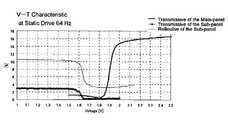
- FIG. 12is a graph of voltages applied to the main display panel and to the sub-display panel, and transmittances.
- a display deviceincludes a first display panel, a second display panel that has a different optimal driver voltage than that of the first display panel, and a driver IC that supplies driver signals in parallel to the first display panel and to the second display panel.
- the driver ICswitches between output of a first driver signal having an optimal driver voltage for the first display panel and a second driver signal having an optimal driver voltage for the second display panel.
- the second display paneltakes on a single color display over its entire screen when the first driver signal is output. For example, when the optimal driver voltage for the second display panel is less than the optimal driver voltage for the first display panel, and when the display mode of the second display panel is a normally white mode, the screen of the second display panel will display black when the first driver signal is input to both display panels.
- the screen of the second display panelwill display white when the first driver signal is input to both display panels.
- the first driver signal and the second driver signalare set so that the driver duty and the driver bias ratio will be optimal for the first display panel and for the second display panel, respectively.
- an electronic device of the present inventionuses a display device having any of the configurations described above.
- FIG 1is a perspective view of a portable electronic device in the form of a clamshell type cellular telephone in an open state.
- a cellular telephone 1uses a main panel 2 in an open state.
- a projection 3places a switch 4 in an on state when the cellular telephone 1 is in a closed state, while the switch 4 is in an off state when the cellular telephone 1 is open.
- a judgementcan thus be made as to whether the cellular telephone 1 is in an open state or in a closed state.
- FIG. 2is a perspective view of a rear surface side of the cellular telephone 1 .
- a sub-panel 5is disposed on the rear surface.
- FIG. 3is a perspective view of the cellular telephone 1 in a closed state. The sub-panel 5 displays time, date, messages received, or calls received.
- FIG. 4is a side view that shows a connection state between the main display panel and the sub-display panel of a double sided liquid crystal display module.
- a drive IC (integrated circuit) 6is mounted on a first FPC (flexible printed circuit) 7 , and is connected to the main display panel 2 .
- a second FCP 8extracts signals from the main display panel 2 , and is connected to the sub-display panel 5 .
- FIG. 5is a side view of the double sided display module with an incorporated back light.
- a back light 9 that uses an LED (not shown) as a light sourceis disposed on a rear surface of the main display panel 2 .
- the second FPC 8 connected to the sub-display panel 5is disposed as bent.
- the back lightis of a type that emits light to two sides.
- FIG. 6is a front view of the liquid crystal display module as seen from the sub-display panel side.
- the sub-display panelis smaller in size than the main display panel.
- the main display panelis a normally black mode, 128 (RGB) ⁇ 160 dot (pixel) transmissive type panel.
- the sub-display panelis a normally white mode, 64 (RGB) ⁇ 96 dot (pixel) semi-transmissive type panel, and has a lower optimal driver voltage than the optimal driver voltage of the main display panel.
- FIG. 7is a conceptual diagram that shows the main display panel, the sub-display panel, and wirings of the driver IC.
- the driver ICoutputs 128 ⁇ 3 (RGB) segmented signals, and 160 common signals.
- 64 ⁇ 3 (RGB) segmented signals and 96 common signals from among the signals output to the main panelare connected to the sub-display panel in parallel with the main display panel.
- FIG. 8is a display image of the main display panel when the cellular telephone is in an open state.
- the driver ICoutputs signals at 1/160 duty, setting an optimal voltage for the main display panel.
- FIG. 9is a display image of the sub-display panel when the cellular telephone is in an open state.
- the 1/160 duty driver voltage that is optimal for the main display panelis applied to the sub-display panel. Accordingly, the liquid crystals of the sub-display panel are placed in an on state whether the driver signal is an on signal or an off signal, and the entire screen or display area of the sub-display panel displays black.
- FIG. 10is a display image of the main panel when the cellular telephone is in a closed state.
- the same voltage as the 1/96 duty optimal driver voltage for the sub-display panelis also applied to the main display panel, in portions where the main display panel and the sub-display panel are connected, when the sub-display panel is performing display.
- the optimal driver voltage of the main display panelis higher than the optimal driver voltage of the sub-display panel. Accordingly, the main display panel does not display anything, whether the optimal driver voltage of the sub-display panel is an on signal or an off signal.
- FIG. 11is a display image of the sub-display panel when the cellular telephone is in a closed state. As described above, the sub-display panel is in an optimal image display state.
- FIG. 12is a graph of voltages of the main display panel and the sub-display panel, and light transmittances.
- the main display panelis a normally black mode display panel
- the sub-display panelis a normally white mode display panel.
- the liquid crystals in the main display panelturn on at 1.95 V, and turn off at 1.85 V.
- the sub-display panelis off from 1.85 V to 1.95 V.
- the liquid crystals in the sub-display panelturn on at 1.70 V, and turn off at 1.60 V.
- the main display panelis off from 1.60 V to 1.70 V. Accordingly, the sub-display panel is completely black when the main display panel performs display, and the main display panel is completely black when the sub-display panel performs display.
- the sub-display panelis a normally white mode display panel in this embodiment, it may also be a normally black mode display panel that uses liquid crystals having an optimal driver voltage that is higher than the optimal driver voltage of the main display panel.
- switchingcan be accomplished between a main display panel and a sub-display panel according to output driver voltages when the main display panel and the sub-display panel are connected in parallel to one driver IC.
- the main display panel and the sub-display panelcan each perform display under optimal driver conditions. Consequently, a driver IC and peripheral components used for the sub-display panel, which are needed for conventional double sided displays having equivalent quality, become unnecessary. A low cost double sided display device can therefore be provided. Further, space is obtained by reducing the number of components. For example, the degree of freedom available for product design increases, such as that for arranging a camera module and making the sub-display panel larger in size, and an attractively finished product can be provided.
Landscapes
- Engineering & Computer Science (AREA)
- Chemical & Material Sciences (AREA)
- Crystallography & Structural Chemistry (AREA)
- Physics & Mathematics (AREA)
- Computer Hardware Design (AREA)
- General Physics & Mathematics (AREA)
- Theoretical Computer Science (AREA)
- Control Of Indicators Other Than Cathode Ray Tubes (AREA)
- Liquid Crystal (AREA)
- Devices For Indicating Variable Information By Combining Individual Elements (AREA)
- Liquid Crystal Display Device Control (AREA)
Abstract
Description
Claims (20)
Applications Claiming Priority (4)
| Application Number | Priority Date | Filing Date | Title |
|---|---|---|---|
| JP2003-349173 | 2003-10-08 | ||
| JP2003349173 | 2003-10-08 | ||
| JP2004291522AJP4681267B2 (en) | 2003-10-08 | 2004-10-04 | Display device and electronic device including the same |
| JP2004-291522 | 2004-10-04 |
Publications (2)
| Publication Number | Publication Date |
|---|---|
| US20050174300A1 US20050174300A1 (en) | 2005-08-11 |
| US7474274B2true US7474274B2 (en) | 2009-01-06 |
Family
ID=34655994
Family Applications (1)
| Application Number | Title | Priority Date | Filing Date |
|---|---|---|---|
| US10/960,167Active2026-04-24US7474274B2 (en) | 2003-10-08 | 2004-10-07 | Display device and electronic device using the same |
Country Status (3)
| Country | Link |
|---|---|
| US (1) | US7474274B2 (en) |
| JP (1) | JP4681267B2 (en) |
| CN (1) | CN1617217A (en) |
Cited By (2)
| Publication number | Priority date | Publication date | Assignee | Title |
|---|---|---|---|---|
| US20070291041A1 (en)* | 2002-10-03 | 2007-12-20 | Nec Electronics Corporation | Apparatus for driving a plurality of display units using common driving circuits |
| US20120105734A1 (en)* | 2010-11-02 | 2012-05-03 | Zakiyaa Jada Johnson | Multi-Panel Display Device |
Families Citing this family (2)
| Publication number | Priority date | Publication date | Assignee | Title |
|---|---|---|---|---|
| JP2007027099A (en)* | 2005-07-13 | 2007-02-01 | Samsung Electronics Co Ltd | Backlight assembly, display substrate, display device having the same, display substrate, and manufacturing method thereof |
| JP5011730B2 (en)* | 2006-01-18 | 2012-08-29 | 富士ゼロックス株式会社 | Image forming apparatus, sub-unit replacement method, and image forming apparatus maintenance method |
Citations (7)
| Publication number | Priority date | Publication date | Assignee | Title |
|---|---|---|---|---|
| US5670970A (en)* | 1993-12-17 | 1997-09-23 | Canon Kabushiki Kaisha | Head-mount display with opposite polarity reversal for left and right sides |
| US5841431A (en)* | 1996-11-15 | 1998-11-24 | Intel Corporation | Application of split- and dual-screen LCD panel design in cellular phones |
| US5881299A (en)* | 1995-11-22 | 1999-03-09 | Kabushiki Kaisha Toshiba | Selectively removing power from multiple display areas of a display unit |
| US6917359B1 (en)* | 1999-03-31 | 2005-07-12 | Minolta Co., Ltd. | Information display device and information display method |
| US20060077116A1 (en)* | 2004-10-08 | 2006-04-13 | Toppoly Optoelectronics Corp. | Display driving circuit and method and multi-panel display using the same |
| US7089040B2 (en)* | 2000-01-27 | 2006-08-08 | Kyocera Corporation | Portable radio communication apparatus |
| US7088355B1 (en)* | 1999-08-31 | 2006-08-08 | Minolta Co., Ltd. | Information display device |
Family Cites Families (4)
| Publication number | Priority date | Publication date | Assignee | Title |
|---|---|---|---|---|
| JP3108616B2 (en)* | 1995-11-01 | 2000-11-13 | シャープ株式会社 | Liquid crystal display device and wireless receiving device provided with liquid crystal display device |
| JP3461716B2 (en)* | 1998-03-23 | 2003-10-27 | シャープ株式会社 | Display device |
| JP2003228358A (en)* | 2002-01-31 | 2003-08-15 | Sanyo Electric Co Ltd | Electronic device |
| JP4794801B2 (en)* | 2002-10-03 | 2011-10-19 | ルネサスエレクトロニクス株式会社 | Display device for portable electronic device |
- 2004
- 2004-10-04JPJP2004291522Apatent/JP4681267B2/ennot_activeExpired - Fee Related
- 2004-10-07USUS10/960,167patent/US7474274B2/enactiveActive
- 2004-10-08CNCN200410100574.2Apatent/CN1617217A/enactivePending
Patent Citations (7)
| Publication number | Priority date | Publication date | Assignee | Title |
|---|---|---|---|---|
| US5670970A (en)* | 1993-12-17 | 1997-09-23 | Canon Kabushiki Kaisha | Head-mount display with opposite polarity reversal for left and right sides |
| US5881299A (en)* | 1995-11-22 | 1999-03-09 | Kabushiki Kaisha Toshiba | Selectively removing power from multiple display areas of a display unit |
| US5841431A (en)* | 1996-11-15 | 1998-11-24 | Intel Corporation | Application of split- and dual-screen LCD panel design in cellular phones |
| US6917359B1 (en)* | 1999-03-31 | 2005-07-12 | Minolta Co., Ltd. | Information display device and information display method |
| US7088355B1 (en)* | 1999-08-31 | 2006-08-08 | Minolta Co., Ltd. | Information display device |
| US7089040B2 (en)* | 2000-01-27 | 2006-08-08 | Kyocera Corporation | Portable radio communication apparatus |
| US20060077116A1 (en)* | 2004-10-08 | 2006-04-13 | Toppoly Optoelectronics Corp. | Display driving circuit and method and multi-panel display using the same |
Cited By (3)
| Publication number | Priority date | Publication date | Assignee | Title |
|---|---|---|---|---|
| US20070291041A1 (en)* | 2002-10-03 | 2007-12-20 | Nec Electronics Corporation | Apparatus for driving a plurality of display units using common driving circuits |
| US7843400B2 (en)* | 2002-10-03 | 2010-11-30 | Renesas Electronics Corporation | Apparatus for driving a plurality of display units using common driving circuits |
| US20120105734A1 (en)* | 2010-11-02 | 2012-05-03 | Zakiyaa Jada Johnson | Multi-Panel Display Device |
Also Published As
| Publication number | Publication date |
|---|---|
| JP2005134890A (en) | 2005-05-26 |
| JP4681267B2 (en) | 2011-05-11 |
| CN1617217A (en) | 2005-05-18 |
| US20050174300A1 (en) | 2005-08-11 |
Similar Documents
| Publication | Publication Date | Title |
|---|---|---|
| US11849613B2 (en) | Display module comprising side wirings and large format display apparatus using the same | |
| US20090009527A1 (en) | Liquid crystal display device and mobile terminal device | |
| JP4298400B2 (en) | Display device | |
| US20130176196A1 (en) | Light Emitting Device | |
| US20090051637A1 (en) | Display devices | |
| US7002652B2 (en) | Transflective liquid crystal display | |
| US7924262B2 (en) | Light source driving apparatus, display device having the same and method of driving a light source | |
| US20040207569A1 (en) | Dual-display panel module with a shared ASIC chip | |
| US7969405B2 (en) | Double-sided LCD panel | |
| KR100550487B1 (en) | Liquid crystal display | |
| US7474274B2 (en) | Display device and electronic device using the same | |
| JP2005070121A (en) | Display apparatus | |
| US20060087477A1 (en) | Multi display device and method of controlling the same | |
| US20060001819A1 (en) | Display device | |
| US20060092095A1 (en) | Multi-display system | |
| US7548219B2 (en) | Display device | |
| US7138964B2 (en) | Mobile unit with dual panel display | |
| KR100742375B1 (en) | Double sided organic light emitting device | |
| JP5196694B2 (en) | Image display device and electronic apparatus equipped with the same | |
| KR101108296B1 (en) | LCD and its driving method | |
| CN120255222A (en) | Display panel, display module, display device | |
| KR101119178B1 (en) | Display | |
| JP2001183998A (en) | Display device | |
| CN120233587A (en) | Display panel, display module, display device | |
| JP2008064781A (en) | Display device |
Legal Events
| Date | Code | Title | Description |
|---|---|---|---|
| AS | Assignment | Owner name:SEIKO INSTRUMENTS INC., JAPAN Free format text:ASSIGNMENT OF ASSIGNORS INTEREST;ASSIGNORS:MATSUHIRA, TSUTOMU;HANAWA, HORIKO;SASAKI, NOBUYUKI;AND OTHERS;REEL/FRAME:016168/0585 Effective date:20041201 | |
| STCF | Information on status: patent grant | Free format text:PATENTED CASE | |
| FPAY | Fee payment | Year of fee payment:4 | |
| FEPP | Fee payment procedure | Free format text:PAYER NUMBER DE-ASSIGNED (ORIGINAL EVENT CODE: RMPN); ENTITY STATUS OF PATENT OWNER: SMALL ENTITY Free format text:PAYOR NUMBER ASSIGNED (ORIGINAL EVENT CODE: ASPN); ENTITY STATUS OF PATENT OWNER: SMALL ENTITY | |
| FEPP | Fee payment procedure | Free format text:PAT HOLDER CLAIMS SMALL ENTITY STATUS, ENTITY STATUS SET TO SMALL (ORIGINAL EVENT CODE: LTOS); ENTITY STATUS OF PATENT OWNER: SMALL ENTITY | |
| AS | Assignment | Owner name:BEIJING METIS TECHNOLOGY SERVICE CENTER (LLP), CHI Free format text:ASSIGNMENT OF ASSIGNORS INTEREST;ASSIGNOR:SEIKO INSTRUMENTS INC.;REEL/FRAME:038593/0418 Effective date:20150918 | |
| FPAY | Fee payment | Year of fee payment:8 | |
| FEPP | Fee payment procedure | Free format text:MAINTENANCE FEE REMINDER MAILED (ORIGINAL EVENT CODE: REM.); ENTITY STATUS OF PATENT OWNER: SMALL ENTITY | |
| FEPP | Fee payment procedure | Free format text:11.5 YR SURCHARGE- LATE PMT W/IN 6 MO, SMALL ENTITY (ORIGINAL EVENT CODE: M2556); ENTITY STATUS OF PATENT OWNER: SMALL ENTITY | |
| MAFP | Maintenance fee payment | Free format text:PAYMENT OF MAINTENANCE FEE, 12TH YR, SMALL ENTITY (ORIGINAL EVENT CODE: M2553); ENTITY STATUS OF PATENT OWNER: SMALL ENTITY Year of fee payment:12 | |
| AS | Assignment | Owner name:DAWNCREST IP LLC, TEXAS Free format text:ASSIGNMENT OF ASSIGNORS INTEREST;ASSIGNOR:BEIJING METIS TECHNOLOGY SERVICE CENTER (LLP);REEL/FRAME:057917/0154 Effective date:20210902 |