US7473653B1 - Methods for producing low stress porous low-k dielectric materials using precursors with organic functional groups - Google Patents
Methods for producing low stress porous low-k dielectric materials using precursors with organic functional groupsDownload PDFInfo
- Publication number
- US7473653B1 US7473653B1US11/764,750US76475007AUS7473653B1US 7473653 B1US7473653 B1US 7473653B1US 76475007 AUS76475007 AUS 76475007AUS 7473653 B1US7473653 B1US 7473653B1
- Authority
- US
- United States
- Prior art keywords
- precursor
- porogen
- structure former
- film
- carbon
- Prior art date
- Legal status (The legal status is an assumption and is not a legal conclusion. Google has not performed a legal analysis and makes no representation as to the accuracy of the status listed.)
- Expired - Fee Related
Links
Images


Classifications
- H—ELECTRICITY
- H01—ELECTRIC ELEMENTS
- H01L—SEMICONDUCTOR DEVICES NOT COVERED BY CLASS H10
- H01L21/00—Processes or apparatus adapted for the manufacture or treatment of semiconductor or solid state devices or of parts thereof
- H01L21/02—Manufacture or treatment of semiconductor devices or of parts thereof
- H01L21/02104—Forming layers
- H01L21/02107—Forming insulating materials on a substrate
- H01L21/02296—Forming insulating materials on a substrate characterised by the treatment performed before or after the formation of the layer
- H01L21/02318—Forming insulating materials on a substrate characterised by the treatment performed before or after the formation of the layer post-treatment
- H01L21/02345—Forming insulating materials on a substrate characterised by the treatment performed before or after the formation of the layer post-treatment treatment by exposure to radiation, e.g. visible light
- H01L21/02348—Forming insulating materials on a substrate characterised by the treatment performed before or after the formation of the layer post-treatment treatment by exposure to radiation, e.g. visible light treatment by exposure to UV light
- H—ELECTRICITY
- H01—ELECTRIC ELEMENTS
- H01L—SEMICONDUCTOR DEVICES NOT COVERED BY CLASS H10
- H01L21/00—Processes or apparatus adapted for the manufacture or treatment of semiconductor or solid state devices or of parts thereof
- H01L21/02—Manufacture or treatment of semiconductor devices or of parts thereof
- H01L21/02104—Forming layers
- H01L21/02107—Forming insulating materials on a substrate
- H01L21/02109—Forming insulating materials on a substrate characterised by the type of layer, e.g. type of material, porous/non-porous, pre-cursors, mixtures or laminates
- H01L21/02112—Forming insulating materials on a substrate characterised by the type of layer, e.g. type of material, porous/non-porous, pre-cursors, mixtures or laminates characterised by the material of the layer
- H01L21/02123—Forming insulating materials on a substrate characterised by the type of layer, e.g. type of material, porous/non-porous, pre-cursors, mixtures or laminates characterised by the material of the layer the material containing silicon
- H01L21/02126—Forming insulating materials on a substrate characterised by the type of layer, e.g. type of material, porous/non-porous, pre-cursors, mixtures or laminates characterised by the material of the layer the material containing silicon the material containing Si, O, and at least one of H, N, C, F, or other non-metal elements, e.g. SiOC, SiOC:H or SiONC
- H—ELECTRICITY
- H01—ELECTRIC ELEMENTS
- H01L—SEMICONDUCTOR DEVICES NOT COVERED BY CLASS H10
- H01L21/00—Processes or apparatus adapted for the manufacture or treatment of semiconductor or solid state devices or of parts thereof
- H01L21/02—Manufacture or treatment of semiconductor devices or of parts thereof
- H01L21/02104—Forming layers
- H01L21/02107—Forming insulating materials on a substrate
- H01L21/02109—Forming insulating materials on a substrate characterised by the type of layer, e.g. type of material, porous/non-porous, pre-cursors, mixtures or laminates
- H01L21/02203—Forming insulating materials on a substrate characterised by the type of layer, e.g. type of material, porous/non-porous, pre-cursors, mixtures or laminates the layer being porous
- H—ELECTRICITY
- H01—ELECTRIC ELEMENTS
- H01L—SEMICONDUCTOR DEVICES NOT COVERED BY CLASS H10
- H01L21/00—Processes or apparatus adapted for the manufacture or treatment of semiconductor or solid state devices or of parts thereof
- H01L21/02—Manufacture or treatment of semiconductor devices or of parts thereof
- H01L21/02104—Forming layers
- H01L21/02107—Forming insulating materials on a substrate
- H01L21/02109—Forming insulating materials on a substrate characterised by the type of layer, e.g. type of material, porous/non-porous, pre-cursors, mixtures or laminates
- H01L21/02205—Forming insulating materials on a substrate characterised by the type of layer, e.g. type of material, porous/non-porous, pre-cursors, mixtures or laminates the layer being characterised by the precursor material for deposition
- H01L21/02208—Forming insulating materials on a substrate characterised by the type of layer, e.g. type of material, porous/non-porous, pre-cursors, mixtures or laminates the layer being characterised by the precursor material for deposition the precursor containing a compound comprising Si
- H01L21/02211—Forming insulating materials on a substrate characterised by the type of layer, e.g. type of material, porous/non-porous, pre-cursors, mixtures or laminates the layer being characterised by the precursor material for deposition the precursor containing a compound comprising Si the compound being a silane, e.g. disilane, methylsilane or chlorosilane
- H—ELECTRICITY
- H01—ELECTRIC ELEMENTS
- H01L—SEMICONDUCTOR DEVICES NOT COVERED BY CLASS H10
- H01L21/00—Processes or apparatus adapted for the manufacture or treatment of semiconductor or solid state devices or of parts thereof
- H01L21/02—Manufacture or treatment of semiconductor devices or of parts thereof
- H01L21/02104—Forming layers
- H01L21/02107—Forming insulating materials on a substrate
- H01L21/02109—Forming insulating materials on a substrate characterised by the type of layer, e.g. type of material, porous/non-porous, pre-cursors, mixtures or laminates
- H01L21/02205—Forming insulating materials on a substrate characterised by the type of layer, e.g. type of material, porous/non-porous, pre-cursors, mixtures or laminates the layer being characterised by the precursor material for deposition
- H01L21/02208—Forming insulating materials on a substrate characterised by the type of layer, e.g. type of material, porous/non-porous, pre-cursors, mixtures or laminates the layer being characterised by the precursor material for deposition the precursor containing a compound comprising Si
- H01L21/02214—Forming insulating materials on a substrate characterised by the type of layer, e.g. type of material, porous/non-porous, pre-cursors, mixtures or laminates the layer being characterised by the precursor material for deposition the precursor containing a compound comprising Si the compound comprising silicon and oxygen
- H01L21/02216—Forming insulating materials on a substrate characterised by the type of layer, e.g. type of material, porous/non-porous, pre-cursors, mixtures or laminates the layer being characterised by the precursor material for deposition the precursor containing a compound comprising Si the compound comprising silicon and oxygen the compound being a molecule comprising at least one silicon-oxygen bond and the compound having hydrogen or an organic group attached to the silicon or oxygen, e.g. a siloxane
- H—ELECTRICITY
- H01—ELECTRIC ELEMENTS
- H01L—SEMICONDUCTOR DEVICES NOT COVERED BY CLASS H10
- H01L21/00—Processes or apparatus adapted for the manufacture or treatment of semiconductor or solid state devices or of parts thereof
- H01L21/02—Manufacture or treatment of semiconductor devices or of parts thereof
- H01L21/02104—Forming layers
- H01L21/02107—Forming insulating materials on a substrate
- H01L21/02225—Forming insulating materials on a substrate characterised by the process for the formation of the insulating layer
- H01L21/0226—Forming insulating materials on a substrate characterised by the process for the formation of the insulating layer formation by a deposition process
- H01L21/02263—Forming insulating materials on a substrate characterised by the process for the formation of the insulating layer formation by a deposition process deposition from the gas or vapour phase
- H01L21/02271—Forming insulating materials on a substrate characterised by the process for the formation of the insulating layer formation by a deposition process deposition from the gas or vapour phase deposition by decomposition or reaction of gaseous or vapour phase compounds, i.e. chemical vapour deposition
- H01L21/02274—Forming insulating materials on a substrate characterised by the process for the formation of the insulating layer formation by a deposition process deposition from the gas or vapour phase deposition by decomposition or reaction of gaseous or vapour phase compounds, i.e. chemical vapour deposition in the presence of a plasma [PECVD]
Definitions
- This inventionrelates to methods for preparing a porous low-k film having low tensile stress and high mechanical strength.
- the methodsinvolve the use of porogen technology. More specifically, the methods involve the deposition of a precursor film using one or more precursors with organic functional groups. Functional groups include moieties with carbon-carbon double or triple bonds and bulky organic groups. Once the precursor film is formed, the porogen is removed, leaving a low-k porous film. Methods of the invention provide a low stress, low-k porous film that can be used as a low-k dielectric layer in integrated circuits.
- Low k dielectricsare conventionally defined as those materials that have a dielectric constant lower than that of silicon dioxide, that is k ⁇ ⁇ 4. Typical methods of obtaining low-k materials include doping silicon dioxide with various hydrocarbons or fluorine. These doping methods, however, generally cannot produce materials with dielectric constants lower than about 2.6. With more and more advanced technology needs, present efforts are focused on developing low-k dielectric materials with k less than 2.5. These ultra low-k dielectrics can be obtained by incorporating air voids within a low-k dielectric, creating a porous dielectric material.
- Methods of fabricating porous dielectricstypically involve forming a composite film (sometimes referred to herein as a “precursor film”) containing two components: a porogen (typically an organic material such as a polymer) and a structure former or dielectric material (e.g., a silicon containing material).
- a porogentypically an organic material such as a polymer
- a structure former or dielectric materiale.g., a silicon containing material
- One issue with producing low-k porous materialsrelates to the fact that generally the more porous the material is (that is, the more air voids within the dielectric matrix), the lower the dielectric constant. In general, a lower dielectric constant is desirable. However, incorporating air voids may also diminish the film's mechanical strength and integrity, including increasing the film's intrinsic residual stress.
- the present inventionaddresses the aforementioned need by providing improved methods of preparing a low stress, low-k dielectric material on a substrate using precursors with various functional groups.
- methodsinvolve (a) forming a precursor film on the substrate, the precursor film comprising a porogen and a structure former, wherein the structure former has one or more carbon-carbon double or triple bonds, and (b) treating the precursor film to facilitate removing the porogen from the precursor film and thereby creating voids within the dielectric material to form the porous low-k dielectric material.
- methodsinvolve (a) forming a precursor film on the substrate, the precursor film comprising a porogen and a structure former, wherein the porogen has at least one bulky organic functional group, and (b) treating the precursor film to facilitate removing the porogen from the precursor film and thereby creating voids within the dielectric material to form the porous low-k dielectric material.
- the structure formerwill contain derivatives of silicon.
- the precursor filmcan be produced by co-depositing the structure former precursor with a porogen precursor or the structure former and porogen can both be obtained from the structure former precursor and no separate porogen precursor is deposited with the structure former precursor.
- Suitable structure former precursors that contain C ⁇ C and/or C ⁇ Cinclude trimethylsilylacetylene (TMSA), bis(trimethylsilyl)acetylene (BTMSA), triethynylcyclotrisiloxane derivatives, trivinylcyclotrisiloxane derivatives, vinylmethyldimethoxysilane (VMDMOS), methyldimethoxysilaneacetylene (MDMSA), methyldiethoxysilaneacetylene (MDESA), dimethylmethoxysilaneacetylene (DMMSA), dimethylethoxysilaneacetylene (DMESA), methylethoxysilane-di-acetylene (MESDA), divinylmethylethoxysilane (DVMEOS), 1,3,5-trivinyl-1,3,5-trimethylcyclotrisiloxane (VMTS) and 1,3,5-trivinyl-1,3,5-triisopropylcyclotrisiloxane (
- the structure former precursormay also have a bulky organic group.
- these bulky organic structure former precursorsinclude, for example, 5-(bicycloheptenyl)methyldimethoxysilane (BMDS), 5-(bicycloheptenyl)triethoxysilane (BTS) and 5-(bicycloheptenyl)diethoxysilaneacetylene (BDS).
- the porogen precursoris preferably an organic material that can be easily removed by subsequent processes.
- One preferred class of porogen precursoris polyfunctional cyclic non-aromatic compounds. More preferably, the polyfunctional cyclic non-aromatic compounds also contains at least one carbon-carbon triple or double bond. Particular examples of preferred compounds are 5-ethylidene-2-norbornene (ENB), 8,8-dimethylfulvene (DMF) and beta-pinene (BP).
- the precursor filmcan be formed using a CVD process (e.g., a plasma enhanced chemical vapor deposition (PECVD) technique), a spin-on process, or another condensed phase method.
- PECVD techniquesare used.
- preferred deposition temperaturestypically range between about 25 and 400 degrees Celsius, more preferably between about 100 and 300 degrees Celsius.
- FIGS. 1A and 1Bare graphs representing percent porosity and pore size as functions of dielectric constant (k) of porous films prepared using methods of the inventions.
- FIGS. 2A-2Care graphs representing the affects of using different precursor concentration on the dielectric constant, amount of porogen and residual film stress for porous films.
- FIG. 3is a graph representing is a graph representing the affects of using different concentrations of structure former precursors on the refractive indexes of porous films.
- FIGS. 4A and 4Bare graphs representing the affects of using different precursor flow rates on the dielectric constant and refractive index of porous films.
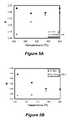
- FIGS. 5A and 5Bare graphs representing the affects of using different deposition temperatures on dielectric constant and refractive index of porous films.
- FIG. 6is a composite graph of three FTIR spectra, one of a precursor film before porogen removal, another of a precursor film after porogen removal using a thermal process, and the third of a precursor film after porogen removal with UV radiation.
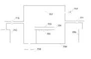
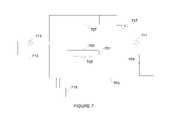
- FIG. 7is a schematic representation of apparatus suitable for porogen removal in accordance with certain embodiments of this invention.
- the present inventioninvolves forming a porous low-k dielectric material by way of a “precursor film” or “precursor layer” that contains a “structure former,” typically a silicon and oxide containing dielectric material, which serves as a backbone of the porous network, and a porogen, which generates the porous regions within the porous network.
- a “structure former”typically a silicon and oxide containing dielectric material, which serves as a backbone of the porous network
- a porogentypically exist as separate phases within the precursor layer.
- the porogenis removed from the precursor film to create a dielectric matrix or porous film.
- the locations within the precursor film where the porogen once residedbecome void locations in the final porous dielectric film.
- a structure former precursor and a porogen precursoris co-deposited on a substrate to create the precursor film.
- the structure former precursor and porogen precursormay be co-deposited in one process or in a multiple-phase process.
- more than one type of structure former precursor molecule and more than one type of porogen precursor moleculemay be used in any suitable combination.
- the structure former precursorcomprises both the structure former and porogen. That is, the structure former precursor contains moieties serving as structure formers covalently bonded to moieties, preferably large bulky organic constituents, serving as the porogen.
- the structure former precursorcan be deposited without a separate porogen precursor to form the precursor layer.
- more than one type or structure former precursormay be used to form the precursor film.
- the present inventioninvolves producing low-k porous dielectric film with improved film mechanical integrity.
- One measure of mechanical integrityis residual stress.
- Residual stressis comprised of an extrinsic stress component and an intrinsic stress component.
- Extrinsic stressis produced from a source external to the film.
- extrinsic stressis typically caused by the mismatch in thermo-mechanical properties between a dielectric layer and the underlying substrate, especially a mismatch in their thermal expansion coefficients. Lowering deposition temperature will minimize the extrinsic stress in a film, as will a smaller mismatch in coefficients of thermal expansion between the film and the substrate.
- Intrinsic stresscan be traced to the film-growth mechanism and the final lattice structure of the dielectric material. From a materials standpoint, the intrinsic stress in porous dielectric films is determined by the integrity of the dielectric backbone structure. The present invention primarily focuses on improving the intrinsic stress of the porous film while maintaining a low dielectric constant.
- the precursor layercomprises a structure former and porogen.
- the structure formerincludes at least two carbon atoms that are double or triple bonded. In these cases, the carbon-carbon double and triple bonds are preferably directly adjacent to the silicon atom in the structure former precursor.
- Many different chemical compositionsmay be used as the structure former precursor.
- the structure former precursorincludes at least silicon and oxygen since in many cases the network backbone is silicon oxide based.
- the structure former precursormay also include other elements such as halides. For relatively thick precursor layers, it will sometimes be desirable to use structure formers that are not opaque to the UV radiation if UV radiation methods are used to subsequently remove the porogen.
- Examples of preferred structure former precursorsinclude various organic silanes and organic siloxanes.
- suitable structure former precursor with carbon-carbon double bondsinclude trivinylcyclotrisiloxane derivatives, tetravinylcyclotetrasiloxane derivatives, vinylmethyldimethoxysilane (VMDMOS) and divinylmethylethoxysilane (DVMEOS).
- VMDMOSvinylmethyldimethoxysilane
- DVMEOSdivinylmethylethoxysilane
- Suitable structure former precursor with carbon-carbon triple bondsinclude triethynylcyclotrisiloxane derivatives, trimethylsilylacetylene (TMSA), bis(trimethylsilyl)acetylene (BTMSA), methyldimethoxysilaneacetylene (MDMSA), methyldiethoxysilaneacetylene (MDESA), dimethylmethoxysilaneacetylene (DMMSA), dimethylethoxysilaneacetylene (DMESA), methylethoxysilane-di-acetylene (MESDA), 1,3,5-trivinyl-1,3,5-trimethylcyclotrisiloxane (VMTS) and 1,3,5-trivinyl-1,3,5-triisopropylcyclotrisiloxane (VPTS).
- TMSAtrimethylsilylacetylene
- BTMSAbis(trimethylsilyl)acetylene
- MDMSAmethyldimethoxysilaneacety
- the structure former precursoradditionally contains bulky organic functional groups.
- the bulky organic functional groupswill be considered part of the porogen in the precursor film since they will also be removed to leave void regions in the resultant porous film.
- these structure former precursors that contain bulky organic functional groupsmay be deposited with or without a porogen precursor. Examples of these types of structure former precursors include 5-(bicycloheptenyl)methyldimethoxysilane (BMDS), 5-(bicycloheptenyl)triethoxysilane (BTS) and 5-(bicycloheptenyl)diethoxysilaneacetylene (BDS).
- BMDS5-(bicycloheptenyl)methyldimethoxysilane
- BTS5-(bicycloheptenyl)triethoxysilane
- BDS5-(bicycloheptenyl)diethoxysilaneacetylene
- carbon-carbon double and triple bonds as part of the structure former precursorpromotes cross-linking, i.e., polymerization, within the structure former, which has been found to strengthen the integrity of the dielectric backbone and reduce internal stress of the film. It is believed that the carbon-carbon double and/or triple bonds promote cross-linking by introducing additional bonds of different length, bonds of different angles. And, in fact, it has been found through this invention that intrinsic stress can be reduced by incorporating carbon-carbon double and/or triple bonds.
- a porogenis any removable material that defines void regions in a dielectric matrix.
- the porogen and corresponding porogen precursorare organic materials.
- One preferred class of porogen precursorsis the polyfunctional cyclic non-aromatic compounds.
- the porogen precursorwill preferably include functional groups such as —CH ⁇ CH 2 , —CH ⁇ CH—, —C ⁇ CH, —C ⁇ C—, —C ⁇ O and/or —COC—.
- One class of suitable compoundsis norbornenes, such as 5-ethylidene-2-norbornene (ENB).
- ENB5-ethylidene-2-norbornene
- TMCP1,2,3,4-tetramethyl-1,3-cyclopentadiene
- the porogenhas at least one bulky organic functional group.
- the bulky organic groupcould originate from the structure former precursor, as mentioned previously, or it could originate from the porogen precursor, if a porogen precursor is used. In other cases, both the structure former precursor and the porogen precursor have bulky organic groups.
- the bulky organic groupwill leave correspondingly sized pores in the resulting dielectric film. As such, to a large degree, one can choose the size of pores and the amount of void regions within the final porous film by the type and size of organic groups incorporated in the precursor film.
- the voids, and therefore the organic portions, i.e., porogenbe evenly distributed throughout the porous material and, to a certain extent, to be sufficiently large so as to incorporate more air in the film and thereby lower the overall dielectric constant of the film.
- the adding voids that are too large or that are not evenly distributedwill sacrifice the integrity of the film.
- numerous suitable compoundscan be classified as having bulky organic constituents, including those compounds having large linear or cyclic groups.
- the bulky organic groupsare three-dimensional polyfunctional groups that are spherical in shape. Examples of some preferable compounds include norbornenes, such as 5-ethylidene-2-norbornene (ENB).
- the structure formerincludes at least two carbon atoms that are double or triple bonded and one or both of the structure former and/or porogen has at least one bulky organic functional group.
- the residual stress reduction provided by the carbon-carbon double and/or triple bonds in the structure former precursoris combined with the low-k properties provided by the large porous regions left by the bulky organic groups.
- any of numerous techniquesmay be used. Typical methods include spin-coating processes, print-on, dip coating, thermal process and chemical vapor deposition—particularly plasma enhanced chemical vapor deposition (PECVD). Depending on the application, the thickness of the precursor film may range between about 30 nanometers and about 5 micrometers. Details of suitable deposition techniques are described in the cross-referenced and related references cited above and which are incorporated herein in their entireties. In preferred embodiments of the present invention, PECVD methods are utilized. It is noted that the invention is not limited to any particular type of deposition method. If PECVD processes are used, the deposition temperatures typically range between about 25 and about 450 degrees Celsius and chamber pressures typically range between about 1 Torr to 10 Torr. Of course, numerous factors dictate optimal deposition temperatures, gas flow rates and other process parameters.
- the thickness of the precursor filmdepends upon the ultimate application. As an example, the thickness may range between about 50 to 1500 angstroms for a hard mask application. For an interlayer dielectric or packaging application, the thickness may range up to about 0.1 to 5 microns. In some cases, extra thickness is required to provide some amount of sacrificial dielectric to accommodate a subsequent planarization step. In some cases, the thickness of the precursor layer may be driven in part by the ability of the UV radiation to penetrate the film and remove the porogen. Therefore relatively thinner precursor layers may be required for some processes.
- any suitable methodmay be used to remove the porogen from the precursor film.
- Preferred methodsgenerally involve treating precursor film in such a manner that the porogen is at least partially decomposed and the decomposition products are volatilized away from the deposited precursor film.
- Typical methodsinclude, for example, thermal processes (both slow and rapid), UV mediated methods wherein the precursor film is exposed to UV light, and e-beam methods.
- the inventionis not limited to any particular type of porogen removal method.
- liquid solvent techniquesmay also be used. Note that the precursor layer formation and porogen removal operations can be conducted in a single vessel or in two separate vessels.
- the resultant porous dielectric filmwill preferably have a dielectric constant less than about 2.7, preferably less than 2.5, and the low tensile stress, as measured by a Tencor FLX 5400 Automated Thin Film Stress Measurement System, will preferably be less than about 50 MPa.
- any number of post porogen removal treatmentsmay be implemented on the porous film.
- a silanol capping processto replace dangling hydroxyl groups with non-polar groups (e.g., alkyl groups) and help the film maintain a low overall dielectric constant may be used. Details of some example suitable silanol capping methods are described in U.S. patent application Ser. No. 10/672,311, which the present application is a continuation-in-part and which is incorporated herein in its entirety.
- Example 1illustrates eight porous films (Films A-F) prepared using different structure former precursors and porogen precursors (if used) using methods in accordance with the invention.
- Examples 2-6illustrate the affects of using various process parameters such as precursor concentrations, flow rates, deposition temperatures and porogen removal techniques to prepare porous films.
- porous filmshave been formed using methods in accordance with the invention.
- the filmswere prepared using a structure former precursor without double or triple carbon-carbon bonds (e.g., DEMS, TMCTS) but with a porogen precursor with a bulky organic group (e.g., ENB, BP) (see Films A, D, E and F).
- ENB and BP porogen precursorshave polyfunctional groups, which can extend their structures in three dimensions and form spherically-shaped, bulky functional polymer.
- the filmwas prepared using a structure former precursor with double or triple carbon-carbon bonds (i.e., BTMSA) and no porogen precursor was used (see Film B below).
- the filmwas prepared using a structure former precursor with double or triple carbon-carbon bonds (i.e., BTMSA) with a porogen precursor having a bulky organic group (i.e., ENB) (see Film C below).
- BTMSAstructure former precursor with double or triple carbon-carbon bonds
- ENBporogen precursor having a bulky organic group
- PECVD methodswere used to deposit the precursor films and UV exposure methods were used to remove the porogen to form the porous films.
- FIGS. 1A and 1Bare graphs showing % porosity and pore size, respectively, as functions of the dielectric constant (k) of resulting porous films. As shown, the percent porosity in the film decreased with increasing k. This is an expected result since increasing the total amount of air voids within the film is expected to decrease the k of the film. In this example, the pore size decreases slightly with increasing k.
- Film BPrecursors: BTMSA structure former precursor only. Deposition conditions: high frequency RF power of 2200 Watts, BTMSA flow rate of 1.5 ccm, CO 2 flow rate of 3000 sccm, chamber pressure kept at 7.5 Torr, and deposition temperature of 350 degrees Celsius. Porogen removal conditions: UV exposure for 2.5 minutes. The resulting porous film had a k value of 2.50.
- Film CPrecursors: BTMSA structure former precursor and ENB porogen precursor.
- Deposition conditionshigh frequency RF power of 1200 Watts and low frequency RF of 300 Watts, BTMSA flow rate of 2 ccm, ENB flow rate of 1 ccm, CO 2 flow rate of 3000 sccm, chamber pressure kept at 7 Torr, and deposition temperature of 285 degrees Celsius.
- Porogen removal conditionsThermal treatment for 4 hours. The resulting porous film had a k value of 2.55 and intrinsic stress value of 46 MPa.
- Film DPrecursors: DEMS structure former precursor and ENB porogen precursor.
- Deposition conditionshigh frequency RF power of 2500 Watts, DEMS flow rate of 2 ccm, ENB flow rate of 2 ccm, CO 2 flow rate of 6000 sccm, chamber pressure kept at 9.5 Torr, and deposition temperature of 250 degrees Celsius.
- Porogen removal conditionsThermal treatment for 4 hours, resulting k value of 2.37.
- Post-porogen removal treatmentUV exposure (1.75 W/cm 2 ) for 4 minutes. The resulting porous film had a k value of 2.39 and hardness value of 1.4 GPa.
- Film EPrecursors: TMCTS structure former precursor and ENB porogen precursor.
- Deposition conditionshigh frequency RF power of 1200 Watts, TMCTS flow rate of 1 ccm, ENB flow rate of 0.5 ccm, CO 2 flow rate of 5000 sccm, chamber pressure kept at 6 Torr, and substrate temperature of 70 degrees Celsius.
- Porogen removal conditionsThermal treatment. The resulting porous film had a k value of 2.48.
- Film FPrecursors: TMCTS structure former precursor and BP porogen precursor.
- Deposition conditionshigh frequency RF power of 1000 Watts, TMCTS flow rate of 1 ccm, BP flow rate of 2 ccm, CO 2 flow rate of 7000 sccm, chamber pressure kept at 7.5 Torr.
- Porogen removal conditionsThermal treatment. The resulting porous film had a k value of 2.5.
- FIGS. 4A and 4Bare graphs showing the affects of using different flow rates of the precursors during PECVD deposition process for five sample films.
- DEMSwas used as the structure former precursor and ENB was used as the porogen precursor in each of the five samples.
- the total flow rate of ENB and DEMS (1:1 ratio)ranged from about 1.9 ccm to about 4.0 ccm.
- FIG. 4Ashows that the k values for the films decreased within increasing total flow rate for the as-deposited (pre-porogen removal) films and for the post-porogen removal films.
- FIG. 4Bshows that the RI remained about the same (around 1.45) as total flow rate increased for the as-deposited film and that the RI slightly decreased as total flow rate increased for the as-deposited film.
- FIGS. 5A and 5Bare graphs showing the affects of using different deposition temperatures during PECVD deposition process for four sample films.
- DEMSwas used as the structure former precursor and ENB was used as the porogen precursor in each of the five samples.
- the deposition temperaturesranged from about 250 to about 400 degrees Celsius.
- FIG. 5Ashows that the k values remained within about 2.78 and 2.87 for the as-deposited films and that the k values increased from about 2.46 to about 2.8 for the post-porogen removal films with increasing deposition temperatures.
- FIG. 5Bshows that the RI remained decreased from about 1.46 to about 1.4 for the as-deposited film and that the RI may have slightly increased from about 1.37 to about 1.4 for the as-deposited film with increasing deposition temperatures.
- FIG. 6is a composite graph of three FTIR spectra of film samples before porogen removal (spectrum 601 ), after a thermal treatment (indicated as “post ann.”) for porogen removal (spectrum 603 ) and after a UV exposure treatment for porogen removal (spectrum 605 ).
- DEMSwas used as the structure former precursor and ENB was used as the porogen precursor for all samples in the same ratios.
- the thermal treatmentinvolved heating the wafer sample to about 425 degrees Celsius for about 4 hours.
- the UV treatmentinvolved exposing the wafer sample to broadband UV light of 1.75 Watts/cm 2 for about 4 minutes. All three spectra exhibit absorption peaks ( 607 ) around 2840 to 3055 cm ⁇ 1 corresponding to the C—H stretch.
- both the thermally treated sample (spectrum 603 ) and the UV treated sample (spectrum 605 )exhibit reductions in the C—H stretch peaks compared to the pre-treated film (spectrum 601 ). It is noted that the UV treated sample (spectrum 605 ) exhibits more of a decrease in the C—H stretch peaks, indicating more porogen removal. Also for all three spectra, the peaks ( 609 ) at 1273 cm ⁇ 1 are attributed to the presence of Si—CH 3 methyl groups, corresponding to the “T” groups ((SiO) 3 Si—CH 3 ) from the DEMS structure former precursor.
- the apparatuswill include one or more chambers (sometimes referred to as process vessels) that house one or more wafers and are suitable for wafer processing.
- at least one chamberwill include a UV source.
- a single chambermay be employed for all operations of the invention or separate chambers may be used.
- Each chambermay house one or more wafers for processing.
- the one or more chambersmaintain the wafer in a defined position or positions (with or without motion within that position, e.g. rotation, vibration, or other agitation) during porogen removal and post porogen removal processes such as anneal and silanol capping, if used.
- the apparatusmay include a heating platen.
- FIG. 7is a schematic diagram of an example chamber system in accordance with the invention. This particular system is configured to use UV light for the porogen removal process. As stated earlier, the invention is not limited to any particular porogen removal methods or associated apparatus.
- a substrate holder 701 and a UV light source 707are housed within a chamber 700 . In alternate embodiments, the light source may be mounted outside the chamber on a window.
- Chamber 700is capable of holding a vacuum and/or containing gases at pressures above atmospheric pressure. Chamber 700 may be one chamber in a multi-chambered system or it may be a stand-alone apparatus.
- Substrate holder 701holds substrate 703 such that it can be irradiated with light from UV light source 707 .
- Substrate holder 701has a heater 705 that can heat the substrate to defined temperatures and can be controlled by a temperature controller (not shown).
- UV light source 707is a xenon lamp or other source of UV radiation of the required characteristics.
- the UV light sourcemay be a lamp or a laser (not shown), such as an excimer laser, capable of providing intense UV light.
- various optical elementsmay be required to direct the UV light toward portions of the substrate. Methods for directing the laser light at different portions of the substrate at different times will be required as well.
- the UV sourcedirects UV radiation on the substrate at an intensity of between about 1 ⁇ W/cm 2 and 10 W/cm 2 in the range of 200 to 400 nanometers.
- FIG. 7is only an example of a suitable apparatus and other apparatuses designed for other methods involved in previous and/or subsequent processes may be used.
- methods of the inventionmay be used with a standard PECVD chamber.
- Some supercritical fluid chamber systemsmay also be used. Many of these systems may also be used to perform the post-porogen removal anneal and/or silanol capping procedures, if used. Obviously, in these cases, the chamber system will likely be pumped out between each of the process steps.
Landscapes
- Engineering & Computer Science (AREA)
- Physics & Mathematics (AREA)
- Condensed Matter Physics & Semiconductors (AREA)
- General Physics & Mathematics (AREA)
- Manufacturing & Machinery (AREA)
- Computer Hardware Design (AREA)
- Microelectronics & Electronic Packaging (AREA)
- Power Engineering (AREA)
- Formation Of Insulating Films (AREA)
- Internal Circuitry In Semiconductor Integrated Circuit Devices (AREA)
- Chemical Vapour Deposition (AREA)
Abstract
Description
This application is a divisional claiming priority under 35 USC 120 from U.S. patent application Ser. No. 10/927,777, filed on Aug. 27, 2004, titled “METHODS FOR PRODUCING LOW STRESS POROUS LOW-K DIELECTRIC MATERIALS USING PRECURSORS WITH ORGANIC FUNCTIONAL GROUPS,” by Wu et al. as inventors, which is a continuation-in-part claiming priority under 35 USC 120 from U.S. patent application Ser. No. 10/672,311, filed on Sep. 26, 2003, which is now U.S. Pat. No. 7,208,389, issued on Apr. 24, 2007, titled “METHOD OF POROGEN REMOVAL FROM POROUS LOW-K FILMS USING UV RADIATION,” by Tipton et al. as inventors, which claims benefit under 35 USC 119 from U.S. Provisional No. 60/469,433, filed on May 9, 2003, titled “METHODS FOR PRODUCING LOW STRESS POROUS LOW-K DIELECTRIC MATERIALS USING PRECURSORS WITH ORGANIC FUNCTIONAL GROUPS,” by Wu et al. as inventors,” and which is a continuation-in-part claiming priority under 35 USC 120 from U.S. patent application Ser. No. 10/404,693, filed on Mar. 31, 2003, titled “METHOD FOR FORMING POROUS FILMS BY POROGEN REMOVAL COMBINED WITH IN SITU SURFACE MODIFICATION,” by Humayun et al. as inventors, which applications are incorporated herein by reference in their entireties for all purposes. This application is also related to U.S. patent application Ser. No. 10/789,103, filed on Feb. 27, 2004, entitled “METHODS FOR PRODUCING LOW-K CDO FILMS WITH LOW RESIDUAL STRESS” by Wu et al. as inventors, which application is incorporated herein by reference in its entirety for all purposes.
This invention relates to methods for preparing a porous low-k film having low tensile stress and high mechanical strength. The methods involve the use of porogen technology. More specifically, the methods involve the deposition of a precursor film using one or more precursors with organic functional groups. Functional groups include moieties with carbon-carbon double or triple bonds and bulky organic groups. Once the precursor film is formed, the porogen is removed, leaving a low-k porous film. Methods of the invention provide a low stress, low-k porous film that can be used as a low-k dielectric layer in integrated circuits.
There is a general need for materials with low dielectric constants (low-k) in the integrated circuit manufacturing industry. Using low-k materials as the inter-metal and/or inter-layer dielectric of conductive interconnects reduces the delay in signal propagation due to capacitive effects. The lower the dielectric constant of the dielectric, the lower the capacitance of the dielectric and the lower the RC delay of the IC.
Low k dielectrics are conventionally defined as those materials that have a dielectric constant lower than that of silicon dioxide, that is k<˜4. Typical methods of obtaining low-k materials include doping silicon dioxide with various hydrocarbons or fluorine. These doping methods, however, generally cannot produce materials with dielectric constants lower than about 2.6. With more and more advanced technology needs, present efforts are focused on developing low-k dielectric materials with k less than 2.5. These ultra low-k dielectrics can be obtained by incorporating air voids within a low-k dielectric, creating a porous dielectric material.
Methods of fabricating porous dielectrics typically involve forming a composite film (sometimes referred to herein as a “precursor film”) containing two components: a porogen (typically an organic material such as a polymer) and a structure former or dielectric material (e.g., a silicon containing material). Once the composite film is formed on the substrate, the porogen component is removed, leaving a structurally intact porous dielectric matrix. Techniques for removing porogens from the composite film typically include, for example, a thermal process in which the substrate is heated to a temperature sufficient for the breakdown and vaporization of the organic porogen.
One issue with producing low-k porous materials relates to the fact that generally the more porous the material is (that is, the more air voids within the dielectric matrix), the lower the dielectric constant. In general, a lower dielectric constant is desirable. However, incorporating air voids may also diminish the film's mechanical strength and integrity, including increasing the film's intrinsic residual stress.
What are needed therefore are improved methods for forming porous dielectric low-k films with reduced tensile stress and improved mechanical integrity.
The present invention addresses the aforementioned need by providing improved methods of preparing a low stress, low-k dielectric material on a substrate using precursors with various functional groups. In some preferred embodiments of the present invention, methods involve (a) forming a precursor film on the substrate, the precursor film comprising a porogen and a structure former, wherein the structure former has one or more carbon-carbon double or triple bonds, and (b) treating the precursor film to facilitate removing the porogen from the precursor film and thereby creating voids within the dielectric material to form the porous low-k dielectric material. In some preferred embodiments, methods involve (a) forming a precursor film on the substrate, the precursor film comprising a porogen and a structure former, wherein the porogen has at least one bulky organic functional group, and (b) treating the precursor film to facilitate removing the porogen from the precursor film and thereby creating voids within the dielectric material to form the porous low-k dielectric material.
In most cases, the structure former will contain derivatives of silicon. The precursor film can be produced by co-depositing the structure former precursor with a porogen precursor or the structure former and porogen can both be obtained from the structure former precursor and no separate porogen precursor is deposited with the structure former precursor.
Examples of suitable structure former precursors that contain C≡C and/or C═C include trimethylsilylacetylene (TMSA), bis(trimethylsilyl)acetylene (BTMSA), triethynylcyclotrisiloxane derivatives, trivinylcyclotrisiloxane derivatives, vinylmethyldimethoxysilane (VMDMOS), methyldimethoxysilaneacetylene (MDMSA), methyldiethoxysilaneacetylene (MDESA), dimethylmethoxysilaneacetylene (DMMSA), dimethylethoxysilaneacetylene (DMESA), methylethoxysilane-di-acetylene (MESDA), divinylmethylethoxysilane (DVMEOS), 1,3,5-trivinyl-1,3,5-trimethylcyclotrisiloxane (VMTS) and 1,3,5-trivinyl-1,3,5-triisopropylcyclotrisiloxane (VPTS). The structure former precursor may also have a bulky organic group. Examples of these bulky organic structure former precursors include, for example, 5-(bicycloheptenyl)methyldimethoxysilane (BMDS), 5-(bicycloheptenyl)triethoxysilane (BTS) and 5-(bicycloheptenyl)diethoxysilaneacetylene (BDS).
The porogen precursor is preferably an organic material that can be easily removed by subsequent processes. One preferred class of porogen precursor is polyfunctional cyclic non-aromatic compounds. More preferably, the polyfunctional cyclic non-aromatic compounds also contains at least one carbon-carbon triple or double bond. Particular examples of preferred compounds are 5-ethylidene-2-norbornene (ENB), 8,8-dimethylfulvene (DMF) and beta-pinene (BP).
The precursor film can be formed using a CVD process (e.g., a plasma enhanced chemical vapor deposition (PECVD) technique), a spin-on process, or another condensed phase method. In preferred embodiments, PECVD techniques are used. For PECVD methods, preferred deposition temperatures typically range between about 25 and 400 degrees Celsius, more preferably between about 100 and 300 degrees Celsius. After the precursor film is formed, treatments such as thermal treatment, plasma treatment, ultraviolet radiation exposure, e-beam exposure, or a combination thereof are used to facilitate removal of the porogen.
These and other features and advantages of the invention will be described in detail below with reference to the associated drawings.
The following detailed description can be more fully understood when considered in conjunction with the drawings in which:
In the following description, numerous specific details are set forth in order to provide a thorough understanding of the present invention, which pertains to formation of porous dielectric materials. The present invention may be practiced without some or all of these specific details. In other instances, well known process operations have not been described in detail to not unnecessarily obscure the present invention. While the invention will be described in conjunction with the specific embodiments, it will be understood that it is not intended to limit the invention to the embodiments.
The present invention involves forming a porous low-k dielectric material by way of a “precursor film” or “precursor layer” that contains a “structure former,” typically a silicon and oxide containing dielectric material, which serves as a backbone of the porous network, and a porogen, which generates the porous regions within the porous network. Hence, the porogen and dielectric matrix typically exist as separate phases within the precursor layer. After the precursor film is formed, the porogen is removed from the precursor film to create a dielectric matrix or porous film. Thus, the locations within the precursor film where the porogen once resided become void locations in the final porous dielectric film.
In methods of the invention, there are two general approaches to forming the precursor film. Both of these approaches should be kept in mind as viable techniques that can be used in accordance with methods of the invention. In one approach, a structure former precursor and a porogen precursor is co-deposited on a substrate to create the precursor film. The structure former precursor and porogen precursor may be co-deposited in one process or in a multiple-phase process. Of course, more than one type of structure former precursor molecule and more than one type of porogen precursor molecule may be used in any suitable combination. In an alternative approach, the structure former precursor comprises both the structure former and porogen. That is, the structure former precursor contains moieties serving as structure formers covalently bonded to moieties, preferably large bulky organic constituents, serving as the porogen. Thus, in the latter approach, the structure former precursor can be deposited without a separate porogen precursor to form the precursor layer. Also in the latter approach, more than one type or structure former precursor may be used to form the precursor film.
The present invention involves producing low-k porous dielectric film with improved film mechanical integrity. One measure of mechanical integrity is residual stress. Residual stress is comprised of an extrinsic stress component and an intrinsic stress component. Extrinsic stress is produced from a source external to the film. In integrated circuits, extrinsic stress is typically caused by the mismatch in thermo-mechanical properties between a dielectric layer and the underlying substrate, especially a mismatch in their thermal expansion coefficients. Lowering deposition temperature will minimize the extrinsic stress in a film, as will a smaller mismatch in coefficients of thermal expansion between the film and the substrate. Intrinsic stress can be traced to the film-growth mechanism and the final lattice structure of the dielectric material. From a materials standpoint, the intrinsic stress in porous dielectric films is determined by the integrity of the dielectric backbone structure. The present invention primarily focuses on improving the intrinsic stress of the porous film while maintaining a low dielectric constant.
As indicated previously, the precursor layer comprises a structure former and porogen. In some preferred embodiments of the present invention, the structure former includes at least two carbon atoms that are double or triple bonded. In these cases, the carbon-carbon double and triple bonds are preferably directly adjacent to the silicon atom in the structure former precursor. Many different chemical compositions may be used as the structure former precursor. In most cases, the structure former precursor includes at least silicon and oxygen since in many cases the network backbone is silicon oxide based. The structure former precursor may also include other elements such as halides. For relatively thick precursor layers, it will sometimes be desirable to use structure formers that are not opaque to the UV radiation if UV radiation methods are used to subsequently remove the porogen.
Examples of preferred structure former precursors include various organic silanes and organic siloxanes. Some specific examples of suitable structure former precursor with carbon-carbon double bonds include trivinylcyclotrisiloxane derivatives, tetravinylcyclotetrasiloxane derivatives, vinylmethyldimethoxysilane (VMDMOS) and divinylmethylethoxysilane (DVMEOS). Some specific examples of suitable structure former precursor with carbon-carbon triple bonds include triethynylcyclotrisiloxane derivatives, trimethylsilylacetylene (TMSA), bis(trimethylsilyl)acetylene (BTMSA), methyldimethoxysilaneacetylene (MDMSA), methyldiethoxysilaneacetylene (MDESA), dimethylmethoxysilaneacetylene (DMMSA), dimethylethoxysilaneacetylene (DMESA), methylethoxysilane-di-acetylene (MESDA), 1,3,5-trivinyl-1,3,5-trimethylcyclotrisiloxane (VMTS) and 1,3,5-trivinyl-1,3,5-triisopropylcyclotrisiloxane (VPTS). In some cases, the structure former precursor additionally contains bulky organic functional groups. Once deposited, the bulky organic functional groups will be considered part of the porogen in the precursor film since they will also be removed to leave void regions in the resultant porous film. As such, these structure former precursors that contain bulky organic functional groups may be deposited with or without a porogen precursor. Examples of these types of structure former precursors include 5-(bicycloheptenyl)methyldimethoxysilane (BMDS), 5-(bicycloheptenyl)triethoxysilane (BTS) and 5-(bicycloheptenyl)diethoxysilaneacetylene (BDS).
Although not wishing to be bound by theory, it is believed that carbon-carbon double and triple bonds as part of the structure former precursor promotes cross-linking, i.e., polymerization, within the structure former, which has been found to strengthen the integrity of the dielectric backbone and reduce internal stress of the film. It is believed that the carbon-carbon double and/or triple bonds promote cross-linking by introducing additional bonds of different length, bonds of different angles. And, in fact, it has been found through this invention that intrinsic stress can be reduced by incorporating carbon-carbon double and/or triple bonds. Some more details as to how carbon-carbon double and triple bonds relate to the intrinsic stress and other mechanical properties of a non-porous dielectric materials can be found in the previously mentioned U.S. patent application Ser. No. 10/789,103, which is incorporated herein in its entirety.
Regarding the porogen, generally, a porogen is any removable material that defines void regions in a dielectric matrix. Frequently, though not necessarily, the porogen and corresponding porogen precursor are organic materials. One preferred class of porogen precursors is the polyfunctional cyclic non-aromatic compounds. In particular, the porogen precursor will preferably include functional groups such as —CH═CH2, —CH═CH—, —C≡CH, —C≡C—, —C═O and/or —COC—. One class of suitable compounds is norbornenes, such as 5-ethylidene-2-norbornene (ENB). Another typical example is 1,2,3,4-tetramethyl-1,3-cyclopentadiene (TMCP) (C9H14). A listing of more porogen precursor compounds can be found in U.S. patent application Ser. No. 10/672,311, which the present application is a continuation-in-part and which is incorporated herein in its entirety.
In some preferred embodiments of the present invention, the porogen has at least one bulky organic functional group. The bulky organic group could originate from the structure former precursor, as mentioned previously, or it could originate from the porogen precursor, if a porogen precursor is used. In other cases, both the structure former precursor and the porogen precursor have bulky organic groups. The bulky organic group will leave correspondingly sized pores in the resulting dielectric film. As such, to a large degree, one can choose the size of pores and the amount of void regions within the final porous film by the type and size of organic groups incorporated in the precursor film. It is generally desirable that the voids, and therefore the organic portions, i.e., porogen, be evenly distributed throughout the porous material and, to a certain extent, to be sufficiently large so as to incorporate more air in the film and thereby lower the overall dielectric constant of the film. Of course, the adding voids that are too large or that are not evenly distributed will sacrifice the integrity of the film. As known in the art, numerous suitable compounds can be classified as having bulky organic constituents, including those compounds having large linear or cyclic groups. In preferred embodiments, the bulky organic groups are three-dimensional polyfunctional groups that are spherical in shape. Examples of some preferable compounds include norbornenes, such as 5-ethylidene-2-norbornene (ENB). Other specific examples include 8,8-dimethylfulvene (DMF) and beta-pinene (BP). Some affects of using various porogen precursors on pore size, porogen concentration and dielectric constant are described byFIGS. 1A ,1B,2A,3A,4A and corresponding descriptions below.
In certain preferred embodiments, the structure former includes at least two carbon atoms that are double or triple bonded and one or both of the structure former and/or porogen has at least one bulky organic functional group. In these cases, the residual stress reduction provided by the carbon-carbon double and/or triple bonds in the structure former precursor is combined with the low-k properties provided by the large porous regions left by the bulky organic groups.
Regarding techniques for depositing the precursor film, any of numerous techniques may be used. Typical methods include spin-coating processes, print-on, dip coating, thermal process and chemical vapor deposition—particularly plasma enhanced chemical vapor deposition (PECVD). Depending on the application, the thickness of the precursor film may range between about 30 nanometers and about 5 micrometers. Details of suitable deposition techniques are described in the cross-referenced and related references cited above and which are incorporated herein in their entireties. In preferred embodiments of the present invention, PECVD methods are utilized. It is noted that the invention is not limited to any particular type of deposition method. If PECVD processes are used, the deposition temperatures typically range between about 25 and about 450 degrees Celsius and chamber pressures typically range between about 1 Torr to 10 Torr. Of course, numerous factors dictate optimal deposition temperatures, gas flow rates and other process parameters.
The thickness of the precursor film (and hence the resulting porous dielectric layer) depends upon the ultimate application. As an example, the thickness may range between about 50 to 1500 angstroms for a hard mask application. For an interlayer dielectric or packaging application, the thickness may range up to about 0.1 to 5 microns. In some cases, extra thickness is required to provide some amount of sacrificial dielectric to accommodate a subsequent planarization step. In some cases, the thickness of the precursor layer may be driven in part by the ability of the UV radiation to penetrate the film and remove the porogen. Therefore relatively thinner precursor layers may be required for some processes.
Any suitable method may be used to remove the porogen from the precursor film. Preferred methods generally involve treating precursor film in such a manner that the porogen is at least partially decomposed and the decomposition products are volatilized away from the deposited precursor film. Typical methods include, for example, thermal processes (both slow and rapid), UV mediated methods wherein the precursor film is exposed to UV light, and e-beam methods. Note, however, the invention is not limited to any particular type of porogen removal method. For example, liquid solvent techniques may also be used. Note that the precursor layer formation and porogen removal operations can be conducted in a single vessel or in two separate vessels. Also, it is possible for a precursor layer formation and porogen removal to occur in one chamber and then for the substrate to be moved to a different chamber where more of the porogen is removed. In general, however, for mechanical simplicity, it is preferred to perform as many operations as possible in a single chamber.
After porogen removal, the resultant porous dielectric film will preferably have a dielectric constant less than about 2.7, preferably less than 2.5, and the low tensile stress, as measured by a Tencor FLX 5400 Automated Thin Film Stress Measurement System, will preferably be less than about 50 MPa.
Note that after the porogen is removed, any number of post porogen removal treatments may be implemented on the porous film. For example, a silanol capping process to replace dangling hydroxyl groups with non-polar groups (e.g., alkyl groups) and help the film maintain a low overall dielectric constant may be used. Details of some example suitable silanol capping methods are described in U.S. patent application Ser. No. 10/672,311, which the present application is a continuation-in-part and which is incorporated herein in its entirety.
The following examples, Examples 1-6, are presented to help illustrate aspects of the invention. It should be understood that these examples are representative only, and that the invention is not limited by the detail set forth in these examples. Note also that the following examples are merely experimental and do not necessarily represent optimized conditions for preparing low-k, low stress porous films.
Example 1 illustrates eight porous films (Films A-F) prepared using different structure former precursors and porogen precursors (if used) using methods in accordance with the invention. Examples 2-6 illustrate the affects of using various process parameters such as precursor concentrations, flow rates, deposition temperatures and porogen removal techniques to prepare porous films.
The following porous films (Films A-F) have been formed using methods in accordance with the invention. In some cases, the films were prepared using a structure former precursor without double or triple carbon-carbon bonds (e.g., DEMS, TMCTS) but with a porogen precursor with a bulky organic group (e.g., ENB, BP) (see Films A, D, E and F). As previously described, ENB and BP porogen precursors have polyfunctional groups, which can extend their structures in three dimensions and form spherically-shaped, bulky functional polymer. In one case, the film was prepared using a structure former precursor with double or triple carbon-carbon bonds (i.e., BTMSA) and no porogen precursor was used (see Film B below). And in one case, the film was prepared using a structure former precursor with double or triple carbon-carbon bonds (i.e., BTMSA) with a porogen precursor having a bulky organic group (i.e., ENB) (see Film C below). The following are descriptions of the precursor compositions and processes conditions for preparing Films A-F, with resulting k values and intrinsic stress/hardness values. In all examples, PECVD methods were used to deposit the precursor films and UV exposure methods were used to remove the porogen to form the porous films.
Films A1, A2 and A3: Three porous films, A1, A2 and A3, were prepared with the following precursors and process conditions using different amounts of porogen precursor and structure former precursor. Precursors: DEMS structure former precursor and ENB is a porogen precursor. Deposition conditions: high frequency RF power of 2500 Watts, ENB flow rate of 3 ccm, DEMS at a flow rate of 2 ccm, CO2flow rate of 6000 sccm, chamber pressure kept at 9.5 Torr, and deposition temperature of 250 degrees Celsius. Porogen removal conditions: UV exposure for 7 minutes.FIGS. 1A and 1B are graphs showing % porosity and pore size, respectively, as functions of the dielectric constant (k) of resulting porous films. As shown, the percent porosity in the film decreased with increasing k. This is an expected result since increasing the total amount of air voids within the film is expected to decrease the k of the film. In this example, the pore size decreases slightly with increasing k.
Film B: Precursors: BTMSA structure former precursor only. Deposition conditions: high frequency RF power of 2200 Watts, BTMSA flow rate of 1.5 ccm, CO2flow rate of 3000 sccm, chamber pressure kept at 7.5 Torr, and deposition temperature of 350 degrees Celsius. Porogen removal conditions: UV exposure for 2.5 minutes. The resulting porous film had a k value of 2.50.
Film C: Precursors: BTMSA structure former precursor and ENB porogen precursor. Deposition conditions: high frequency RF power of 1200 Watts and low frequency RF of 300 Watts, BTMSA flow rate of 2 ccm, ENB flow rate of 1 ccm, CO2flow rate of 3000 sccm, chamber pressure kept at 7 Torr, and deposition temperature of 285 degrees Celsius. Porogen removal conditions: Thermal treatment for 4 hours. The resulting porous film had a k value of 2.55 and intrinsic stress value of 46 MPa.
Film D: Precursors: DEMS structure former precursor and ENB porogen precursor. Deposition conditions: high frequency RF power of 2500 Watts, DEMS flow rate of 2 ccm, ENB flow rate of 2 ccm, CO2flow rate of 6000 sccm, chamber pressure kept at 9.5 Torr, and deposition temperature of 250 degrees Celsius. Porogen removal conditions: Thermal treatment for 4 hours, resulting k value of 2.37. Post-porogen removal treatment: UV exposure (1.75 W/cm2) for 4 minutes. The resulting porous film had a k value of 2.39 and hardness value of 1.4 GPa.
Film E: Precursors: TMCTS structure former precursor and ENB porogen precursor. Deposition conditions: high frequency RF power of 1200 Watts, TMCTS flow rate of 1 ccm, ENB flow rate of 0.5 ccm, CO2flow rate of 5000 sccm, chamber pressure kept at 6 Torr, and substrate temperature of 70 degrees Celsius. Porogen removal conditions: Thermal treatment. The resulting porous film had a k value of 2.48.
Film F: Precursors: TMCTS structure former precursor and BP porogen precursor. Deposition conditions: high frequency RF power of 1000 Watts, TMCTS flow rate of 1 ccm, BP flow rate of 2 ccm, CO2flow rate of 7000 sccm, chamber pressure kept at 7.5 Torr. Porogen removal conditions: Thermal treatment. The resulting porous film had a k value of 2.5.
The present invention can be implemented in many different types of apparatus. Generally, the apparatus will include one or more chambers (sometimes referred to as process vessels) that house one or more wafers and are suitable for wafer processing. In some cases, at least one chamber will include a UV source. A single chamber may be employed for all operations of the invention or separate chambers may be used. Each chamber may house one or more wafers for processing. The one or more chambers maintain the wafer in a defined position or positions (with or without motion within that position, e.g. rotation, vibration, or other agitation) during porogen removal and post porogen removal processes such as anneal and silanol capping, if used. For certain operations in which the wafer is to be heated, the apparatus may include a heating platen.
UVlight source 707 is a xenon lamp or other source of UV radiation of the required characteristics. As indicated above, the UV light source may be a lamp or a laser (not shown), such as an excimer laser, capable of providing intense UV light. In cases where a laser is used, various optical elements may be required to direct the UV light toward portions of the substrate. Methods for directing the laser light at different portions of the substrate at different times will be required as well. In a specific embodiment, the UV source directs UV radiation on the substrate at an intensity of between about 1 μW/cm2and 10 W/cm2in the range of 200 to 400 nanometers.
Note that the apparatus depicted inFIG. 7 is only an example of a suitable apparatus and other apparatuses designed for other methods involved in previous and/or subsequent processes may be used. For example, methods of the invention may be used with a standard PECVD chamber. Some supercritical fluid chamber systems may also be used. Many of these systems may also be used to perform the post-porogen removal anneal and/or silanol capping procedures, if used. Obviously, in these cases, the chamber system will likely be pumped out between each of the process steps.
While this invention has been described in terms of several embodiments, there are alterations, modifications, permutations, and substitute equivalents, which fall within the scope of this invention. It should also be noted that there are many alternative ways of implementing the methods and apparatuses of the present invention. It is therefore intended that the following appended claims be interpreted as including all such alterations, modifications, permutations, and substitute equivalents as fall within the true spirit and scope of the present invention. The use of the singular in the claims does not mean “only one,” but rather “one or more,” unless otherwise stated in the claims.
Claims (18)
1. A method of preparing a porous low-k dielectric material on a substrate, the method comprising:
forming a precursor film on the substrate, the precursor film comprising a porogen and a structure former, wherein the structure former has one or more carbon-carbon double or triple aliphatic bonds; and
treating the precursor film to facilitate removing the porogen from the precursor film and thereby creating voids within the dielectric material to form the porous low-k dielectric material.
2. The method ofclaim 1 , wherein the structure former comprises silicon.
3. The method ofclaim 1 , wherein the precursor film is produced by co-depositing a structure former precursor with a porogen precursor.
4. The method ofclaim 3 , wherein the structure former precursor is a molecule containing at least one silicon atom bonded to a carbon-carbon double bond or a carbon-carbon triple bond.
5. The method ofclaim 3 , wherein the structure former precursor is trimethylsilylacetylene (TMSA), bis(trimethylsilyl)acetylene (BTMSA), vinylmethyldimethoxysilane (VMDMOS), methyldimethoxysilaneacetylene (MDMSA), methyldiethoxysilaneacetylene (MDESA), dimethylmethoxysilaneacetylene (DMMSA), dimethylethoxysilaneacetylene (DMESA) or methylethoxysilane-di-acetylene (MESDA), divinylmethylethoxysilane (DVMEOS).
6. The method ofclaim 3 , wherein the structure former precursor has a bulky organic functional group.
7. The method ofclaim 6 , wherein the structure former precursor is 5-(bicycloheptenyl)methyldimethoxysilane (BMDS), 5-(bicycloheptenyl)triethoxysilane (BTS) or 5-(bicycloheptenyl)diethoxysilaneacetylene (BDS).
8. The method ofclaim 3 , wherein the porogen precursor is a polyfunctional cyclic non-aromatic compound.
9. The method ofclaim 8 , wherein the polyfunctional cyclic non-aromatic compound is 5-ethylidene-2-norbornene (ENB), 8,8-dimethylfulvene (DMF) or beta-pinene (BP).
10. The method ofclaim 1 , wherein the structure former and porogen are both obtained from a structure former precursor.
11. The method ofclaim 10 , wherein the structure former precursor has a bulky organic group.
12. The method ofclaim 11 , wherein the structure former precursor is 5-(bicycloheptenyl)methyldimethoxysilane (BMDS), 5-(bicycloheptenyl)triethoxysilane (BTS) or 5-(bicycloheptenyl)diethoxysilaneacetylene (BDS).
13. The method ofclaim 1 , wherein the precursor film is formed by a chemical vapor deposition process.
14. The method ofclaim 13 , wherein the deposition temperature during chemical vapor deposition ranges between about 25 and about 450 degrees Celsius.
15. The method ofclaim 1 , wherein the precursor film is formed by a spin-on technique.
16. The method ofclaim 1 , wherein treating the precursor film to facilitate removing the porogen from the precursor film involves a thermal treatment, ultraviolet radiation exposure, e-beam exposure, or a combination thereof.
17. The method ofclaim 1 , wherein the dielectric constant of the porous low-k dielectric material is less than about 2.7.
18. The method ofclaim 1 , wherein the tensile stress of the porous low-k dielectric material is less than about 55 MPa.
Priority Applications (3)
| Application Number | Priority Date | Filing Date | Title |
|---|---|---|---|
| US11/764,750US7473653B1 (en) | 2003-03-31 | 2007-06-18 | Methods for producing low stress porous low-k dielectric materials using precursors with organic functional groups |
| US12/348,791US7799705B1 (en) | 2003-03-31 | 2009-01-05 | Methods for producing low stress porous low-k dielectric materials using precursors with organic functional groups |
| US12/479,114US7923385B2 (en) | 2003-03-31 | 2009-06-05 | Methods for producing low stress porous and CDO low-K dielectric materials using precursors with organic functional groups |
Applications Claiming Priority (5)
| Application Number | Priority Date | Filing Date | Title |
|---|---|---|---|
| US40469303A | 2003-03-31 | 2003-03-31 | |
| US46943303P | 2003-05-09 | 2003-05-09 | |
| US10/672,311US7208389B1 (en) | 2003-03-31 | 2003-09-26 | Method of porogen removal from porous low-k films using UV radiation |
| US10/927,777US7241704B1 (en) | 2003-03-31 | 2004-08-27 | Methods for producing low stress porous low-k dielectric materials using precursors with organic functional groups |
| US11/764,750US7473653B1 (en) | 2003-03-31 | 2007-06-18 | Methods for producing low stress porous low-k dielectric materials using precursors with organic functional groups |
Related Parent Applications (1)
| Application Number | Title | Priority Date | Filing Date |
|---|---|---|---|
| US10/927,777DivisionUS7241704B1 (en) | 2003-03-31 | 2004-08-27 | Methods for producing low stress porous low-k dielectric materials using precursors with organic functional groups |
Related Child Applications (1)
| Application Number | Title | Priority Date | Filing Date |
|---|---|---|---|
| US12/348,791ContinuationUS7799705B1 (en) | 2003-03-31 | 2009-01-05 | Methods for producing low stress porous low-k dielectric materials using precursors with organic functional groups |
Publications (1)
| Publication Number | Publication Date |
|---|---|
| US7473653B1true US7473653B1 (en) | 2009-01-06 |
Family
ID=37950766
Family Applications (4)
| Application Number | Title | Priority Date | Filing Date |
|---|---|---|---|
| US10/672,311Expired - Fee RelatedUS7208389B1 (en) | 2003-03-31 | 2003-09-26 | Method of porogen removal from porous low-k films using UV radiation |
| US11/764,750Expired - Fee RelatedUS7473653B1 (en) | 2003-03-31 | 2007-06-18 | Methods for producing low stress porous low-k dielectric materials using precursors with organic functional groups |
| US12/348,791Expired - Fee RelatedUS7799705B1 (en) | 2003-03-31 | 2009-01-05 | Methods for producing low stress porous low-k dielectric materials using precursors with organic functional groups |
| US12/479,114Expired - Fee RelatedUS7923385B2 (en) | 2003-03-31 | 2009-06-05 | Methods for producing low stress porous and CDO low-K dielectric materials using precursors with organic functional groups |
Family Applications Before (1)
| Application Number | Title | Priority Date | Filing Date |
|---|---|---|---|
| US10/672,311Expired - Fee RelatedUS7208389B1 (en) | 2003-03-31 | 2003-09-26 | Method of porogen removal from porous low-k films using UV radiation |
Family Applications After (2)
| Application Number | Title | Priority Date | Filing Date |
|---|---|---|---|
| US12/348,791Expired - Fee RelatedUS7799705B1 (en) | 2003-03-31 | 2009-01-05 | Methods for producing low stress porous low-k dielectric materials using precursors with organic functional groups |
| US12/479,114Expired - Fee RelatedUS7923385B2 (en) | 2003-03-31 | 2009-06-05 | Methods for producing low stress porous and CDO low-K dielectric materials using precursors with organic functional groups |
Country Status (1)
| Country | Link |
|---|---|
| US (4) | US7208389B1 (en) |
Cited By (8)
| Publication number | Priority date | Publication date | Assignee | Title |
|---|---|---|---|---|
| US20080188088A1 (en)* | 2007-02-07 | 2008-08-07 | United Microelectronics Corp. | Forming method and structure of porous low-k layer, interconnect process and interconnect structure |
| US20090239390A1 (en)* | 2003-03-31 | 2009-09-24 | Novellus Systems, Inc. | Methods for producing low stress porous and cdo low-k dielectric materials using precursors with organic functional groups |
| US7695765B1 (en) | 2004-11-12 | 2010-04-13 | Novellus Systems, Inc. | Methods for producing low-stress carbon-doped oxide films with improved integration properties |
| US7737525B1 (en) | 2004-03-11 | 2010-06-15 | Novellus Systems, Inc. | Method for producing low-K CDO films |
| US7781351B1 (en) | 2004-04-07 | 2010-08-24 | Novellus Systems, Inc. | Methods for producing low-k carbon doped oxide films with low residual stress |
| US7906174B1 (en) | 2006-12-07 | 2011-03-15 | Novellus Systems, Inc. | PECVD methods for producing ultra low-k dielectric films using UV treatment |
| US7972976B1 (en) | 2005-01-31 | 2011-07-05 | Novellus Systems, Inc. | VLSI fabrication processes for introducing pores into dielectric materials |
| US20120118204A1 (en)* | 2010-11-17 | 2012-05-17 | Cheng-Jye Chu | Method for preparing low k material and film thereof |
Families Citing this family (452)
| Publication number | Priority date | Publication date | Assignee | Title |
|---|---|---|---|---|
| US7541200B1 (en) | 2002-01-24 | 2009-06-02 | Novellus Systems, Inc. | Treatment of low k films with a silylating agent for damage repair |
| US7404990B2 (en)* | 2002-11-14 | 2008-07-29 | Air Products And Chemicals, Inc. | Non-thermal process for forming porous low dielectric constant films |
| US20050161060A1 (en)* | 2004-01-23 | 2005-07-28 | Johnson Andrew D. | Cleaning CVD chambers following deposition of porogen-containing materials |
| US20050227502A1 (en)* | 2004-04-12 | 2005-10-13 | Applied Materials, Inc. | Method for forming an ultra low dielectric film by forming an organosilicon matrix and large porogens as a template for increased porosity |
| US7253125B1 (en) | 2004-04-16 | 2007-08-07 | Novellus Systems, Inc. | Method to improve mechanical strength of low-k dielectric film using modulated UV exposure |
| US7422776B2 (en)* | 2004-08-24 | 2008-09-09 | Applied Materials, Inc. | Low temperature process to produce low-K dielectrics with low stress by plasma-enhanced chemical vapor deposition (PECVD) |
| US9659769B1 (en) | 2004-10-22 | 2017-05-23 | Novellus Systems, Inc. | Tensile dielectric films using UV curing |
| US7790633B1 (en) | 2004-10-26 | 2010-09-07 | Novellus Systems, Inc. | Sequential deposition/anneal film densification method |
| US7510982B1 (en) | 2005-01-31 | 2009-03-31 | Novellus Systems, Inc. | Creation of porosity in low-k films by photo-disassociation of imbedded nanoparticles |
| US20060220251A1 (en)* | 2005-03-31 | 2006-10-05 | Grant Kloster | Reducing internal film stress in dielectric film |
| US8282768B1 (en) | 2005-04-26 | 2012-10-09 | Novellus Systems, Inc. | Purging of porogen from UV cure chamber |
| US8454750B1 (en) | 2005-04-26 | 2013-06-04 | Novellus Systems, Inc. | Multi-station sequential curing of dielectric films |
| US8980769B1 (en) | 2005-04-26 | 2015-03-17 | Novellus Systems, Inc. | Multi-station sequential curing of dielectric films |
| US8889233B1 (en) | 2005-04-26 | 2014-11-18 | Novellus Systems, Inc. | Method for reducing stress in porous dielectric films |
| US8137465B1 (en) | 2005-04-26 | 2012-03-20 | Novellus Systems, Inc. | Single-chamber sequential curing of semiconductor wafers |
| US7892985B1 (en) | 2005-11-15 | 2011-02-22 | Novellus Systems, Inc. | Method for porogen removal and mechanical strength enhancement of low-k carbon doped silicon oxide using low thermal budget microwave curing |
| US20070134435A1 (en)* | 2005-12-13 | 2007-06-14 | Ahn Sang H | Method to improve the ashing/wet etch damage resistance and integration stability of low dielectric constant films |
| US7851232B2 (en)* | 2006-10-30 | 2010-12-14 | Novellus Systems, Inc. | UV treatment for carbon-containing low-k dielectric repair in semiconductor processing |
| US10037905B2 (en) | 2009-11-12 | 2018-07-31 | Novellus Systems, Inc. | UV and reducing treatment for K recovery and surface clean in semiconductor processing |
| US8465991B2 (en)* | 2006-10-30 | 2013-06-18 | Novellus Systems, Inc. | Carbon containing low-k dielectric constant recovery using UV treatment |
| US8053375B1 (en)* | 2006-11-03 | 2011-11-08 | Advanced Technology Materials, Inc. | Super-dry reagent compositions for formation of ultra low k films |
| US7723226B2 (en)* | 2007-01-17 | 2010-05-25 | Taiwan Semiconductor Manufacturing Company, Ltd. | Interconnects containing bilayer porous low-k dielectrics using different porogen to structure former ratio |
| JP5142538B2 (en)* | 2007-01-26 | 2013-02-13 | 株式会社東芝 | Manufacturing method of semiconductor device |
| US20080188074A1 (en)* | 2007-02-06 | 2008-08-07 | I-I Chen | Peeling-free porous capping material |
| FR2912938B1 (en)* | 2007-02-23 | 2010-11-05 | Commissariat Energie Atomique | PROCESS FOR PREPARING STRUCTURED MATERIAL BY ELECTROMAGNETIC AND / OR PHOTONIC PROCESSING |
| US20080220619A1 (en)* | 2007-03-09 | 2008-09-11 | Asm Japan K.K. | Method for increasing mechanical strength of dielectric film by using sequential combination of two types of uv irradiation |
| US8173537B1 (en) | 2007-03-29 | 2012-05-08 | Novellus Systems, Inc. | Methods for reducing UV and dielectric diffusion barrier interaction |
| US8242028B1 (en) | 2007-04-03 | 2012-08-14 | Novellus Systems, Inc. | UV treatment of etch stop and hard mask films for selectivity and hermeticity enhancement |
| US7622162B1 (en) | 2007-06-07 | 2009-11-24 | Novellus Systems, Inc. | UV treatment of STI films for increasing tensile stress |
| US8211510B1 (en) | 2007-08-31 | 2012-07-03 | Novellus Systems, Inc. | Cascaded cure approach to fabricate highly tensile silicon nitride films |
| US8338315B2 (en)* | 2008-02-26 | 2012-12-25 | Axcelis Technologies, Inc. | Processes for curing silicon based low-k dielectric materials |
| US8124522B1 (en)* | 2008-04-11 | 2012-02-28 | Novellus Systems, Inc. | Reducing UV and dielectric diffusion barrier interaction through the modulation of optical properties |
| FR2931015B1 (en)* | 2008-05-06 | 2010-08-20 | Commissariat Energie Atomique | METHOD FOR PRODUCING AIR CAVITIES IN MICROSTRUCTURES, PARTICULARLY OF THE TYPE OF AIR CAVITY INTERCONNECTION STRUCTURES FOR AN INTEGRATED CIRCUIT |
| US9050623B1 (en) | 2008-09-12 | 2015-06-09 | Novellus Systems, Inc. | Progressive UV cure |
| US10378106B2 (en) | 2008-11-14 | 2019-08-13 | Asm Ip Holding B.V. | Method of forming insulation film by modified PEALD |
| SG174296A1 (en) | 2009-03-10 | 2011-10-28 | Air Liquide | Cyclic amino compounds for low-k silylation |
| US9394608B2 (en) | 2009-04-06 | 2016-07-19 | Asm America, Inc. | Semiconductor processing reactor and components thereof |
| US8802201B2 (en) | 2009-08-14 | 2014-08-12 | Asm America, Inc. | Systems and methods for thin-film deposition of metal oxides using excited nitrogen-oxygen species |
| US8247332B2 (en) | 2009-12-04 | 2012-08-21 | Novellus Systems, Inc. | Hardmask materials |
| CN102859666B (en)* | 2010-02-09 | 2015-05-13 | 西江大学校产学协力团 | Method for manufacturing a nanoporous ultra-low dielectric thin film including a high-temperature ozone treatment and nanoporous ultra-low dielectric thin film manufactured by the method |
| US8349746B2 (en)* | 2010-02-23 | 2013-01-08 | Applied Materials, Inc. | Microelectronic structure including a low k dielectric and a method of controlling carbon distribution in the structure |
| CN102770580A (en)* | 2010-02-25 | 2012-11-07 | 应用材料公司 | Ultra-low dielectric materials formed by plasma enhanced chemical vapor deposition using hybrid precursors containing silicon with organofunctional groups |
| US9312155B2 (en) | 2011-06-06 | 2016-04-12 | Asm Japan K.K. | High-throughput semiconductor-processing apparatus equipped with multiple dual-chamber modules |
| CN102427019A (en)* | 2011-06-17 | 2012-04-25 | 上海华力微电子有限公司 | Method for implementing high-performance metal-oxide-metal by using ultra-low dielectric constant thin film |
| US9793148B2 (en) | 2011-06-22 | 2017-10-17 | Asm Japan K.K. | Method for positioning wafers in multiple wafer transport |
| US10364496B2 (en) | 2011-06-27 | 2019-07-30 | Asm Ip Holding B.V. | Dual section module having shared and unshared mass flow controllers |
| US10854498B2 (en) | 2011-07-15 | 2020-12-01 | Asm Ip Holding B.V. | Wafer-supporting device and method for producing same |
| US20130023129A1 (en) | 2011-07-20 | 2013-01-24 | Asm America, Inc. | Pressure transmitter for a semiconductor processing environment |
| US8551892B2 (en) | 2011-07-27 | 2013-10-08 | Asm Japan K.K. | Method for reducing dielectric constant of film using direct plasma of hydrogen |
| US9017481B1 (en) | 2011-10-28 | 2015-04-28 | Asm America, Inc. | Process feed management for semiconductor substrate processing |
| US8946830B2 (en) | 2012-04-04 | 2015-02-03 | Asm Ip Holdings B.V. | Metal oxide protective layer for a semiconductor device |
| US10832904B2 (en) | 2012-06-12 | 2020-11-10 | Lam Research Corporation | Remote plasma based deposition of oxygen doped silicon carbide films |
| US9234276B2 (en) | 2013-05-31 | 2016-01-12 | Novellus Systems, Inc. | Method to obtain SiC class of films of desired composition and film properties |
| US10211310B2 (en) | 2012-06-12 | 2019-02-19 | Novellus Systems, Inc. | Remote plasma based deposition of SiOC class of films |
| US10325773B2 (en) | 2012-06-12 | 2019-06-18 | Novellus Systems, Inc. | Conformal deposition of silicon carbide films |
| US9558931B2 (en) | 2012-07-27 | 2017-01-31 | Asm Ip Holding B.V. | System and method for gas-phase sulfur passivation of a semiconductor surface |
| US9659799B2 (en) | 2012-08-28 | 2017-05-23 | Asm Ip Holding B.V. | Systems and methods for dynamic semiconductor process scheduling |
| US9021985B2 (en) | 2012-09-12 | 2015-05-05 | Asm Ip Holdings B.V. | Process gas management for an inductively-coupled plasma deposition reactor |
| US9324811B2 (en) | 2012-09-26 | 2016-04-26 | Asm Ip Holding B.V. | Structures and devices including a tensile-stressed silicon arsenic layer and methods of forming same |
| US10714315B2 (en) | 2012-10-12 | 2020-07-14 | Asm Ip Holdings B.V. | Semiconductor reaction chamber showerhead |
| US9337068B2 (en) | 2012-12-18 | 2016-05-10 | Lam Research Corporation | Oxygen-containing ceramic hard masks and associated wet-cleans |
| US9640416B2 (en) | 2012-12-26 | 2017-05-02 | Asm Ip Holding B.V. | Single-and dual-chamber module-attachable wafer-handling chamber |
| US9018108B2 (en) | 2013-01-25 | 2015-04-28 | Applied Materials, Inc. | Low shrinkage dielectric films |
| US20160376700A1 (en) | 2013-02-01 | 2016-12-29 | Asm Ip Holding B.V. | System for treatment of deposition reactor |
| US9589770B2 (en) | 2013-03-08 | 2017-03-07 | Asm Ip Holding B.V. | Method and systems for in-situ formation of intermediate reactive species |
| US9484191B2 (en) | 2013-03-08 | 2016-11-01 | Asm Ip Holding B.V. | Pulsed remote plasma method and system |
| US10297442B2 (en) | 2013-05-31 | 2019-05-21 | Lam Research Corporation | Remote plasma based deposition of graded or multi-layered silicon carbide film |
| KR102053350B1 (en) | 2013-06-13 | 2019-12-06 | 삼성전자주식회사 | Method of Semiconductor Device Having a low-k dielectric |
| US8993054B2 (en) | 2013-07-12 | 2015-03-31 | Asm Ip Holding B.V. | Method and system to reduce outgassing in a reaction chamber |
| US9018111B2 (en) | 2013-07-22 | 2015-04-28 | Asm Ip Holding B.V. | Semiconductor reaction chamber with plasma capabilities |
| US9793115B2 (en) | 2013-08-14 | 2017-10-17 | Asm Ip Holding B.V. | Structures and devices including germanium-tin films and methods of forming same |
| US9240412B2 (en) | 2013-09-27 | 2016-01-19 | Asm Ip Holding B.V. | Semiconductor structure and device and methods of forming same using selective epitaxial process |
| US9556516B2 (en) | 2013-10-09 | 2017-01-31 | ASM IP Holding B.V | Method for forming Ti-containing film by PEALD using TDMAT or TDEAT |
| US9093265B2 (en)* | 2013-10-15 | 2015-07-28 | Taiwan Semiconductor Manufacturing Co., Ltd. | High UV curing efficiency for low-k dielectrics |
| US10179947B2 (en) | 2013-11-26 | 2019-01-15 | Asm Ip Holding B.V. | Method for forming conformal nitrided, oxidized, or carbonized dielectric film by atomic layer deposition |
| WO2015105633A1 (en)* | 2014-01-13 | 2015-07-16 | Applied Materials, Inc. | Carbon dioxide and carbon monoxide mediated curing of low k films to increase hardness and modulus |
| US10683571B2 (en) | 2014-02-25 | 2020-06-16 | Asm Ip Holding B.V. | Gas supply manifold and method of supplying gases to chamber using same |
| US9453614B2 (en)* | 2014-03-17 | 2016-09-27 | Lam Research Corporation | Systems and methods for cooling and removing reactants from a substrate processing chamber |
| US9447498B2 (en) | 2014-03-18 | 2016-09-20 | Asm Ip Holding B.V. | Method for performing uniform processing in gas system-sharing multiple reaction chambers |
| US10167557B2 (en) | 2014-03-18 | 2019-01-01 | Asm Ip Holding B.V. | Gas distribution system, reactor including the system, and methods of using the same |
| US11015245B2 (en) | 2014-03-19 | 2021-05-25 | Asm Ip Holding B.V. | Gas-phase reactor and system having exhaust plenum and components thereof |
| US9404587B2 (en) | 2014-04-24 | 2016-08-02 | ASM IP Holding B.V | Lockout tagout for semiconductor vacuum valve |
| US10858737B2 (en) | 2014-07-28 | 2020-12-08 | Asm Ip Holding B.V. | Showerhead assembly and components thereof |
| US9543180B2 (en) | 2014-08-01 | 2017-01-10 | Asm Ip Holding B.V. | Apparatus and method for transporting wafers between wafer carrier and process tool under vacuum |
| US9890456B2 (en) | 2014-08-21 | 2018-02-13 | Asm Ip Holding B.V. | Method and system for in situ formation of gas-phase compounds |
| US10941490B2 (en) | 2014-10-07 | 2021-03-09 | Asm Ip Holding B.V. | Multiple temperature range susceptor, assembly, reactor and system including the susceptor, and methods of using the same |
| US9657845B2 (en) | 2014-10-07 | 2017-05-23 | Asm Ip Holding B.V. | Variable conductance gas distribution apparatus and method |
| US20160138160A1 (en)* | 2014-11-18 | 2016-05-19 | Lam Research Corporation | Reactive ultraviolet thermal processing of low dielectric constant materials |
| KR102300403B1 (en) | 2014-11-19 | 2021-09-09 | 에이에스엠 아이피 홀딩 비.브이. | Method of depositing thin film |
| KR102263121B1 (en) | 2014-12-22 | 2021-06-09 | 에이에스엠 아이피 홀딩 비.브이. | Semiconductor device and manufacuring method thereof |
| US9478415B2 (en) | 2015-02-13 | 2016-10-25 | Asm Ip Holding B.V. | Method for forming film having low resistance and shallow junction depth |
| US10240236B2 (en) | 2015-03-06 | 2019-03-26 | Lam Research Corporation | Clean resistant windows for ultraviolet thermal processing |
| US10529542B2 (en) | 2015-03-11 | 2020-01-07 | Asm Ip Holdings B.V. | Cross-flow reactor and method |
| US10276355B2 (en) | 2015-03-12 | 2019-04-30 | Asm Ip Holding B.V. | Multi-zone reactor, system including the reactor, and method of using the same |
| US20160314964A1 (en) | 2015-04-21 | 2016-10-27 | Lam Research Corporation | Gap fill using carbon-based films |
| US10458018B2 (en) | 2015-06-26 | 2019-10-29 | Asm Ip Holding B.V. | Structures including metal carbide material, devices including the structures, and methods of forming same |
| US10600673B2 (en) | 2015-07-07 | 2020-03-24 | Asm Ip Holding B.V. | Magnetic susceptor to baseplate seal |
| US9899291B2 (en) | 2015-07-13 | 2018-02-20 | Asm Ip Holding B.V. | Method for protecting layer by forming hydrocarbon-based extremely thin film |
| US10043661B2 (en) | 2015-07-13 | 2018-08-07 | Asm Ip Holding B.V. | Method for protecting layer by forming hydrocarbon-based extremely thin film |
| US10083836B2 (en) | 2015-07-24 | 2018-09-25 | Asm Ip Holding B.V. | Formation of boron-doped titanium metal films with high work function |
| US10087525B2 (en) | 2015-08-04 | 2018-10-02 | Asm Ip Holding B.V. | Variable gap hard stop design |
| US9647114B2 (en) | 2015-08-14 | 2017-05-09 | Asm Ip Holding B.V. | Methods of forming highly p-type doped germanium tin films and structures and devices including the films |
| US9711345B2 (en) | 2015-08-25 | 2017-07-18 | Asm Ip Holding B.V. | Method for forming aluminum nitride-based film by PEALD |
| US9960072B2 (en) | 2015-09-29 | 2018-05-01 | Asm Ip Holding B.V. | Variable adjustment for precise matching of multiple chamber cavity housings |
| US9909214B2 (en) | 2015-10-15 | 2018-03-06 | Asm Ip Holding B.V. | Method for depositing dielectric film in trenches by PEALD |
| US10211308B2 (en) | 2015-10-21 | 2019-02-19 | Asm Ip Holding B.V. | NbMC layers |
| US10322384B2 (en) | 2015-11-09 | 2019-06-18 | Asm Ip Holding B.V. | Counter flow mixer for process chamber |
| US9455138B1 (en) | 2015-11-10 | 2016-09-27 | Asm Ip Holding B.V. | Method for forming dielectric film in trenches by PEALD using H-containing gas |
| US9905420B2 (en) | 2015-12-01 | 2018-02-27 | Asm Ip Holding B.V. | Methods of forming silicon germanium tin films and structures and devices including the films |
| US9607837B1 (en) | 2015-12-21 | 2017-03-28 | Asm Ip Holding B.V. | Method for forming silicon oxide cap layer for solid state diffusion process |
| US9627221B1 (en) | 2015-12-28 | 2017-04-18 | Asm Ip Holding B.V. | Continuous process incorporating atomic layer etching |
| US9735024B2 (en) | 2015-12-28 | 2017-08-15 | Asm Ip Holding B.V. | Method of atomic layer etching using functional group-containing fluorocarbon |
| US11139308B2 (en) | 2015-12-29 | 2021-10-05 | Asm Ip Holding B.V. | Atomic layer deposition of III-V compounds to form V-NAND devices |
| US10468251B2 (en) | 2016-02-19 | 2019-11-05 | Asm Ip Holding B.V. | Method for forming spacers using silicon nitride film for spacer-defined multiple patterning |
| US10529554B2 (en) | 2016-02-19 | 2020-01-07 | Asm Ip Holding B.V. | Method for forming silicon nitride film selectively on sidewalls or flat surfaces of trenches |
| US9754779B1 (en) | 2016-02-19 | 2017-09-05 | Asm Ip Holding B.V. | Method for forming silicon nitride film selectively on sidewalls or flat surfaces of trenches |
| US10501866B2 (en) | 2016-03-09 | 2019-12-10 | Asm Ip Holding B.V. | Gas distribution apparatus for improved film uniformity in an epitaxial system |
| US10343920B2 (en) | 2016-03-18 | 2019-07-09 | Asm Ip Holding B.V. | Aligned carbon nanotubes |
| US9892913B2 (en) | 2016-03-24 | 2018-02-13 | Asm Ip Holding B.V. | Radial and thickness control via biased multi-port injection settings |
| US10190213B2 (en) | 2016-04-21 | 2019-01-29 | Asm Ip Holding B.V. | Deposition of metal borides |
| US10865475B2 (en) | 2016-04-21 | 2020-12-15 | Asm Ip Holding B.V. | Deposition of metal borides and silicides |
| US10087522B2 (en) | 2016-04-21 | 2018-10-02 | Asm Ip Holding B.V. | Deposition of metal borides |
| US10032628B2 (en) | 2016-05-02 | 2018-07-24 | Asm Ip Holding B.V. | Source/drain performance through conformal solid state doping |
| US10367080B2 (en) | 2016-05-02 | 2019-07-30 | Asm Ip Holding B.V. | Method of forming a germanium oxynitride film |
| KR102592471B1 (en) | 2016-05-17 | 2023-10-20 | 에이에스엠 아이피 홀딩 비.브이. | Method of forming metal interconnection and method of fabricating semiconductor device using the same |
| US11453943B2 (en) | 2016-05-25 | 2022-09-27 | Asm Ip Holding B.V. | Method for forming carbon-containing silicon/metal oxide or nitride film by ALD using silicon precursor and hydrocarbon precursor |
| US10388509B2 (en) | 2016-06-28 | 2019-08-20 | Asm Ip Holding B.V. | Formation of epitaxial layers via dislocation filtering |
| US10612137B2 (en) | 2016-07-08 | 2020-04-07 | Asm Ip Holdings B.V. | Organic reactants for atomic layer deposition |
| US9859151B1 (en) | 2016-07-08 | 2018-01-02 | Asm Ip Holding B.V. | Selective film deposition method to form air gaps |
| US9793135B1 (en) | 2016-07-14 | 2017-10-17 | ASM IP Holding B.V | Method of cyclic dry etching using etchant film |
| US10714385B2 (en) | 2016-07-19 | 2020-07-14 | Asm Ip Holding B.V. | Selective deposition of tungsten |
| KR102354490B1 (en) | 2016-07-27 | 2022-01-21 | 에이에스엠 아이피 홀딩 비.브이. | Method of processing a substrate |
| US9887082B1 (en) | 2016-07-28 | 2018-02-06 | Asm Ip Holding B.V. | Method and apparatus for filling a gap |
| US10395919B2 (en) | 2016-07-28 | 2019-08-27 | Asm Ip Holding B.V. | Method and apparatus for filling a gap |
| KR102532607B1 (en) | 2016-07-28 | 2023-05-15 | 에이에스엠 아이피 홀딩 비.브이. | Substrate processing apparatus and method of operating the same |
| US9812320B1 (en) | 2016-07-28 | 2017-11-07 | Asm Ip Holding B.V. | Method and apparatus for filling a gap |
| US10177025B2 (en) | 2016-07-28 | 2019-01-08 | Asm Ip Holding B.V. | Method and apparatus for filling a gap |
| US10090316B2 (en) | 2016-09-01 | 2018-10-02 | Asm Ip Holding B.V. | 3D stacked multilayer semiconductor memory using doped select transistor channel |
| US10090150B2 (en) | 2016-09-06 | 2018-10-02 | Wisconsin Alumni Research Foundation | Low dielectric constant (low-k) dielectric and method of forming the same |
| US9847221B1 (en)* | 2016-09-29 | 2017-12-19 | Lam Research Corporation | Low temperature formation of high quality silicon oxide films in semiconductor device manufacturing |
| US10410943B2 (en) | 2016-10-13 | 2019-09-10 | Asm Ip Holding B.V. | Method for passivating a surface of a semiconductor and related systems |
| US10643826B2 (en) | 2016-10-26 | 2020-05-05 | Asm Ip Holdings B.V. | Methods for thermally calibrating reaction chambers |
| US11532757B2 (en) | 2016-10-27 | 2022-12-20 | Asm Ip Holding B.V. | Deposition of charge trapping layers |
| US10714350B2 (en) | 2016-11-01 | 2020-07-14 | ASM IP Holdings, B.V. | Methods for forming a transition metal niobium nitride film on a substrate by atomic layer deposition and related semiconductor device structures |
| US10435790B2 (en) | 2016-11-01 | 2019-10-08 | Asm Ip Holding B.V. | Method of subatmospheric plasma-enhanced ALD using capacitively coupled electrodes with narrow gap |
| US10643904B2 (en) | 2016-11-01 | 2020-05-05 | Asm Ip Holdings B.V. | Methods for forming a semiconductor device and related semiconductor device structures |
| US10229833B2 (en) | 2016-11-01 | 2019-03-12 | Asm Ip Holding B.V. | Methods for forming a transition metal nitride film on a substrate by atomic layer deposition and related semiconductor device structures |
| US10134757B2 (en) | 2016-11-07 | 2018-11-20 | Asm Ip Holding B.V. | Method of processing a substrate and a device manufactured by using the method |
| KR102546317B1 (en) | 2016-11-15 | 2023-06-21 | 에이에스엠 아이피 홀딩 비.브이. | Gas supply unit and substrate processing apparatus including the same |
| US10002787B2 (en) | 2016-11-23 | 2018-06-19 | Lam Research Corporation | Staircase encapsulation in 3D NAND fabrication |
| US10340135B2 (en) | 2016-11-28 | 2019-07-02 | Asm Ip Holding B.V. | Method of topologically restricted plasma-enhanced cyclic deposition of silicon or metal nitride |
| KR102762543B1 (en) | 2016-12-14 | 2025-02-05 | 에이에스엠 아이피 홀딩 비.브이. | Substrate processing apparatus |
| US11447861B2 (en) | 2016-12-15 | 2022-09-20 | Asm Ip Holding B.V. | Sequential infiltration synthesis apparatus and a method of forming a patterned structure |
| US9916980B1 (en) | 2016-12-15 | 2018-03-13 | Asm Ip Holding B.V. | Method of forming a structure on a substrate |
| US11581186B2 (en) | 2016-12-15 | 2023-02-14 | Asm Ip Holding B.V. | Sequential infiltration synthesis apparatus |
| US9837270B1 (en) | 2016-12-16 | 2017-12-05 | Lam Research Corporation | Densification of silicon carbide film using remote plasma treatment |
| KR102700194B1 (en) | 2016-12-19 | 2024-08-28 | 에이에스엠 아이피 홀딩 비.브이. | Substrate processing apparatus |
| US10269558B2 (en) | 2016-12-22 | 2019-04-23 | Asm Ip Holding B.V. | Method of forming a structure on a substrate |
| US10354857B2 (en) | 2016-12-23 | 2019-07-16 | Lam Research Corporation | High power low pressure UV bulb with plasma resistant coating |
| US10867788B2 (en) | 2016-12-28 | 2020-12-15 | Asm Ip Holding B.V. | Method of forming a structure on a substrate |
| US11390950B2 (en) | 2017-01-10 | 2022-07-19 | Asm Ip Holding B.V. | Reactor system and method to reduce residue buildup during a film deposition process |
| US10655221B2 (en) | 2017-02-09 | 2020-05-19 | Asm Ip Holding B.V. | Method for depositing oxide film by thermal ALD and PEALD |
| US10468261B2 (en) | 2017-02-15 | 2019-11-05 | Asm Ip Holding B.V. | Methods for forming a metallic film on a substrate by cyclical deposition and related semiconductor device structures |
| US10283353B2 (en) | 2017-03-29 | 2019-05-07 | Asm Ip Holding B.V. | Method of reforming insulating film deposited on substrate with recess pattern |
| US10529563B2 (en) | 2017-03-29 | 2020-01-07 | Asm Ip Holdings B.V. | Method for forming doped metal oxide films on a substrate by cyclical deposition and related semiconductor device structures |
| US10103040B1 (en) | 2017-03-31 | 2018-10-16 | Asm Ip Holding B.V. | Apparatus and method for manufacturing a semiconductor device |
| USD830981S1 (en) | 2017-04-07 | 2018-10-16 | Asm Ip Holding B.V. | Susceptor for semiconductor substrate processing apparatus |
| KR102457289B1 (en) | 2017-04-25 | 2022-10-21 | 에이에스엠 아이피 홀딩 비.브이. | Method for depositing a thin film and manufacturing a semiconductor device |
| US10892156B2 (en) | 2017-05-08 | 2021-01-12 | Asm Ip Holding B.V. | Methods for forming a silicon nitride film on a substrate and related semiconductor device structures |
| US10446393B2 (en) | 2017-05-08 | 2019-10-15 | Asm Ip Holding B.V. | Methods for forming silicon-containing epitaxial layers and related semiconductor device structures |
| US10770286B2 (en) | 2017-05-08 | 2020-09-08 | Asm Ip Holdings B.V. | Methods for selectively forming a silicon nitride film on a substrate and related semiconductor device structures |
| US10504742B2 (en) | 2017-05-31 | 2019-12-10 | Asm Ip Holding B.V. | Method of atomic layer etching using hydrogen plasma |
| US10886123B2 (en) | 2017-06-02 | 2021-01-05 | Asm Ip Holding B.V. | Methods for forming low temperature semiconductor layers and related semiconductor device structures |
| US12040200B2 (en) | 2017-06-20 | 2024-07-16 | Asm Ip Holding B.V. | Semiconductor processing apparatus and methods for calibrating a semiconductor processing apparatus |
| US11306395B2 (en) | 2017-06-28 | 2022-04-19 | Asm Ip Holding B.V. | Methods for depositing a transition metal nitride film on a substrate by atomic layer deposition and related deposition apparatus |
| US10685834B2 (en) | 2017-07-05 | 2020-06-16 | Asm Ip Holdings B.V. | Methods for forming a silicon germanium tin layer and related semiconductor device structures |
| KR20190009245A (en) | 2017-07-18 | 2019-01-28 | 에이에스엠 아이피 홀딩 비.브이. | Methods for forming a semiconductor device structure and related semiconductor device structures |
| US11374112B2 (en) | 2017-07-19 | 2022-06-28 | Asm Ip Holding B.V. | Method for depositing a group IV semiconductor and related semiconductor device structures |
| US10541333B2 (en) | 2017-07-19 | 2020-01-21 | Asm Ip Holding B.V. | Method for depositing a group IV semiconductor and related semiconductor device structures |
| US11018002B2 (en) | 2017-07-19 | 2021-05-25 | Asm Ip Holding B.V. | Method for selectively depositing a Group IV semiconductor and related semiconductor device structures |
| US10312055B2 (en) | 2017-07-26 | 2019-06-04 | Asm Ip Holding B.V. | Method of depositing film by PEALD using negative bias |
| US10605530B2 (en) | 2017-07-26 | 2020-03-31 | Asm Ip Holding B.V. | Assembly of a liner and a flange for a vertical furnace as well as the liner and the vertical furnace |
| US10590535B2 (en) | 2017-07-26 | 2020-03-17 | Asm Ip Holdings B.V. | Chemical treatment, deposition and/or infiltration apparatus and method for using the same |
| TWI815813B (en) | 2017-08-04 | 2023-09-21 | 荷蘭商Asm智慧財產控股公司 | Showerhead assembly for distributing a gas within a reaction chamber |
| US10770336B2 (en) | 2017-08-08 | 2020-09-08 | Asm Ip Holding B.V. | Substrate lift mechanism and reactor including same |
| US10692741B2 (en) | 2017-08-08 | 2020-06-23 | Asm Ip Holdings B.V. | Radiation shield |
| US10249524B2 (en) | 2017-08-09 | 2019-04-02 | Asm Ip Holding B.V. | Cassette holder assembly for a substrate cassette and holding member for use in such assembly |
| US11139191B2 (en) | 2017-08-09 | 2021-10-05 | Asm Ip Holding B.V. | Storage apparatus for storing cassettes for substrates and processing apparatus equipped therewith |
| US11769682B2 (en) | 2017-08-09 | 2023-09-26 | Asm Ip Holding B.V. | Storage apparatus for storing cassettes for substrates and processing apparatus equipped therewith |
| US10236177B1 (en) | 2017-08-22 | 2019-03-19 | ASM IP Holding B.V.. | Methods for depositing a doped germanium tin semiconductor and related semiconductor device structures |
| USD900036S1 (en) | 2017-08-24 | 2020-10-27 | Asm Ip Holding B.V. | Heater electrical connector and adapter |
| US11830730B2 (en) | 2017-08-29 | 2023-11-28 | Asm Ip Holding B.V. | Layer forming method and apparatus |
| US11056344B2 (en) | 2017-08-30 | 2021-07-06 | Asm Ip Holding B.V. | Layer forming method |
| US11295980B2 (en) | 2017-08-30 | 2022-04-05 | Asm Ip Holding B.V. | Methods for depositing a molybdenum metal film over a dielectric surface of a substrate by a cyclical deposition process and related semiconductor device structures |
| KR102491945B1 (en) | 2017-08-30 | 2023-01-26 | 에이에스엠 아이피 홀딩 비.브이. | Substrate processing apparatus |
| KR102401446B1 (en) | 2017-08-31 | 2022-05-24 | 에이에스엠 아이피 홀딩 비.브이. | Substrate processing apparatus |
| US10607895B2 (en) | 2017-09-18 | 2020-03-31 | Asm Ip Holdings B.V. | Method for forming a semiconductor device structure comprising a gate fill metal |
| KR102630301B1 (en) | 2017-09-21 | 2024-01-29 | 에이에스엠 아이피 홀딩 비.브이. | Method of sequential infiltration synthesis treatment of infiltrateable material and structures and devices formed using same |
| US10844484B2 (en) | 2017-09-22 | 2020-11-24 | Asm Ip Holding B.V. | Apparatus for dispensing a vapor phase reactant to a reaction chamber and related methods |
| US10658205B2 (en) | 2017-09-28 | 2020-05-19 | Asm Ip Holdings B.V. | Chemical dispensing apparatus and methods for dispensing a chemical to a reaction chamber |
| US10403504B2 (en) | 2017-10-05 | 2019-09-03 | Asm Ip Holding B.V. | Method for selectively depositing a metallic film on a substrate |
| US10319588B2 (en) | 2017-10-10 | 2019-06-11 | Asm Ip Holding B.V. | Method for depositing a metal chalcogenide on a substrate by cyclical deposition |
| KR102470206B1 (en) | 2017-10-13 | 2022-11-23 | 삼성디스플레이 주식회사 | Manufacturing method for metal oxide and display device comprising the metal oxide |
| US10923344B2 (en) | 2017-10-30 | 2021-02-16 | Asm Ip Holding B.V. | Methods for forming a semiconductor structure and related semiconductor structures |
| US10910262B2 (en) | 2017-11-16 | 2021-02-02 | Asm Ip Holding B.V. | Method of selectively depositing a capping layer structure on a semiconductor device structure |
| KR102443047B1 (en) | 2017-11-16 | 2022-09-14 | 에이에스엠 아이피 홀딩 비.브이. | Method of processing a substrate and a device manufactured by the same |
| US11022879B2 (en) | 2017-11-24 | 2021-06-01 | Asm Ip Holding B.V. | Method of forming an enhanced unexposed photoresist layer |
| WO2019103613A1 (en) | 2017-11-27 | 2019-05-31 | Asm Ip Holding B.V. | A storage device for storing wafer cassettes for use with a batch furnace |
| CN111344522B (en) | 2017-11-27 | 2022-04-12 | 阿斯莫Ip控股公司 | Including clean mini-environment device |
| US10290508B1 (en) | 2017-12-05 | 2019-05-14 | Asm Ip Holding B.V. | Method for forming vertical spacers for spacer-defined patterning |
| US10872771B2 (en) | 2018-01-16 | 2020-12-22 | Asm Ip Holding B. V. | Method for depositing a material film on a substrate within a reaction chamber by a cyclical deposition process and related device structures |
| TWI799494B (en) | 2018-01-19 | 2023-04-21 | 荷蘭商Asm 智慧財產控股公司 | Deposition method |
| KR102695659B1 (en) | 2018-01-19 | 2024-08-14 | 에이에스엠 아이피 홀딩 비.브이. | Method for depositing a gap filling layer by plasma assisted deposition |
| USD903477S1 (en) | 2018-01-24 | 2020-12-01 | Asm Ip Holdings B.V. | Metal clamp |
| US11018047B2 (en) | 2018-01-25 | 2021-05-25 | Asm Ip Holding B.V. | Hybrid lift pin |
| US10535516B2 (en) | 2018-02-01 | 2020-01-14 | Asm Ip Holdings B.V. | Method for depositing a semiconductor structure on a surface of a substrate and related semiconductor structures |
| USD880437S1 (en) | 2018-02-01 | 2020-04-07 | Asm Ip Holding B.V. | Gas supply plate for semiconductor manufacturing apparatus |
| US11081345B2 (en) | 2018-02-06 | 2021-08-03 | Asm Ip Holding B.V. | Method of post-deposition treatment for silicon oxide film |
| WO2019158960A1 (en) | 2018-02-14 | 2019-08-22 | Asm Ip Holding B.V. | A method for depositing a ruthenium-containing film on a substrate by a cyclical deposition process |
| US10896820B2 (en) | 2018-02-14 | 2021-01-19 | Asm Ip Holding B.V. | Method for depositing a ruthenium-containing film on a substrate by a cyclical deposition process |
| US10731249B2 (en) | 2018-02-15 | 2020-08-04 | Asm Ip Holding B.V. | Method of forming a transition metal containing film on a substrate by a cyclical deposition process, a method for supplying a transition metal halide compound to a reaction chamber, and related vapor deposition apparatus |
| KR102636427B1 (en) | 2018-02-20 | 2024-02-13 | 에이에스엠 아이피 홀딩 비.브이. | Substrate processing method and apparatus |
| US10658181B2 (en) | 2018-02-20 | 2020-05-19 | Asm Ip Holding B.V. | Method of spacer-defined direct patterning in semiconductor fabrication |
| US10975470B2 (en) | 2018-02-23 | 2021-04-13 | Asm Ip Holding B.V. | Apparatus for detecting or monitoring for a chemical precursor in a high temperature environment |
| US11473195B2 (en) | 2018-03-01 | 2022-10-18 | Asm Ip Holding B.V. | Semiconductor processing apparatus and a method for processing a substrate |
| US11629406B2 (en) | 2018-03-09 | 2023-04-18 | Asm Ip Holding B.V. | Semiconductor processing apparatus comprising one or more pyrometers for measuring a temperature of a substrate during transfer of the substrate |
| US11114283B2 (en) | 2018-03-16 | 2021-09-07 | Asm Ip Holding B.V. | Reactor, system including the reactor, and methods of manufacturing and using same |
| KR102646467B1 (en) | 2018-03-27 | 2024-03-11 | 에이에스엠 아이피 홀딩 비.브이. | Method of forming an electrode on a substrate and a semiconductor device structure including an electrode |
| US11088002B2 (en) | 2018-03-29 | 2021-08-10 | Asm Ip Holding B.V. | Substrate rack and a substrate processing system and method |
| US11230766B2 (en) | 2018-03-29 | 2022-01-25 | Asm Ip Holding B.V. | Substrate processing apparatus and method |
| US10510536B2 (en) | 2018-03-29 | 2019-12-17 | Asm Ip Holding B.V. | Method of depositing a co-doped polysilicon film on a surface of a substrate within a reaction chamber |
| KR102501472B1 (en) | 2018-03-30 | 2023-02-20 | 에이에스엠 아이피 홀딩 비.브이. | Substrate processing method |
| KR102600229B1 (en) | 2018-04-09 | 2023-11-10 | 에이에스엠 아이피 홀딩 비.브이. | Substrate supporting device, substrate processing apparatus including the same and substrate processing method |
| WO2019199682A1 (en)* | 2018-04-09 | 2019-10-17 | Lam Research Corporation | Modifying hydrophobicity of a wafer surface using an organosilicon precursor |
| US12025484B2 (en) | 2018-05-08 | 2024-07-02 | Asm Ip Holding B.V. | Thin film forming method |
| TWI811348B (en) | 2018-05-08 | 2023-08-11 | 荷蘭商Asm 智慧財產控股公司 | Methods for depositing an oxide film on a substrate by a cyclical deposition process and related device structures |
| US12272527B2 (en) | 2018-05-09 | 2025-04-08 | Asm Ip Holding B.V. | Apparatus for use with hydrogen radicals and method of using same |
| KR20190129718A (en) | 2018-05-11 | 2019-11-20 | 에이에스엠 아이피 홀딩 비.브이. | Methods for forming a doped metal carbide film on a substrate and related semiconductor device structures |
| KR102596988B1 (en) | 2018-05-28 | 2023-10-31 | 에이에스엠 아이피 홀딩 비.브이. | Method of processing a substrate and a device manufactured by the same |
| US11718913B2 (en) | 2018-06-04 | 2023-08-08 | Asm Ip Holding B.V. | Gas distribution system and reactor system including same |
| TWI840362B (en) | 2018-06-04 | 2024-05-01 | 荷蘭商Asm Ip私人控股有限公司 | Wafer handling chamber with moisture reduction |
| US11286562B2 (en) | 2018-06-08 | 2022-03-29 | Asm Ip Holding B.V. | Gas-phase chemical reactor and method of using same |
| KR102568797B1 (en) | 2018-06-21 | 2023-08-21 | 에이에스엠 아이피 홀딩 비.브이. | Substrate processing system |
| US10797133B2 (en) | 2018-06-21 | 2020-10-06 | Asm Ip Holding B.V. | Method for depositing a phosphorus doped silicon arsenide film and related semiconductor device structures |
| KR102854019B1 (en) | 2018-06-27 | 2025-09-02 | 에이에스엠 아이피 홀딩 비.브이. | Periodic deposition method for forming a metal-containing material and films and structures comprising the metal-containing material |
| TWI873894B (en) | 2018-06-27 | 2025-02-21 | 荷蘭商Asm Ip私人控股有限公司 | Cyclic deposition methods for forming metal-containing material and films and structures including the metal-containing material |
| US10612136B2 (en) | 2018-06-29 | 2020-04-07 | ASM IP Holding, B.V. | Temperature-controlled flange and reactor system including same |
| KR102686758B1 (en) | 2018-06-29 | 2024-07-18 | 에이에스엠 아이피 홀딩 비.브이. | Method for depositing a thin film and manufacturing a semiconductor device |
| US10388513B1 (en) | 2018-07-03 | 2019-08-20 | Asm Ip Holding B.V. | Method for depositing silicon-free carbon-containing film as gap-fill layer by pulse plasma-assisted deposition |
| US10755922B2 (en) | 2018-07-03 | 2020-08-25 | Asm Ip Holding B.V. | Method for depositing silicon-free carbon-containing film as gap-fill layer by pulse plasma-assisted deposition |
| US10767789B2 (en) | 2018-07-16 | 2020-09-08 | Asm Ip Holding B.V. | Diaphragm valves, valve components, and methods for forming valve components |
| US10483099B1 (en) | 2018-07-26 | 2019-11-19 | Asm Ip Holding B.V. | Method for forming thermally stable organosilicon polymer film |
| US11053591B2 (en) | 2018-08-06 | 2021-07-06 | Asm Ip Holding B.V. | Multi-port gas injection system and reactor system including same |
| US10883175B2 (en) | 2018-08-09 | 2021-01-05 | Asm Ip Holding B.V. | Vertical furnace for processing substrates and a liner for use therein |
| US10829852B2 (en) | 2018-08-16 | 2020-11-10 | Asm Ip Holding B.V. | Gas distribution device for a wafer processing apparatus |
| US11430674B2 (en) | 2018-08-22 | 2022-08-30 | Asm Ip Holding B.V. | Sensor array, apparatus for dispensing a vapor phase reactant to a reaction chamber and related methods |
| CN112513321A (en)* | 2018-08-29 | 2021-03-16 | 应用材料公司 | non-UV high hardness low dielectric constant film deposition |
| KR102707956B1 (en) | 2018-09-11 | 2024-09-19 | 에이에스엠 아이피 홀딩 비.브이. | Method for deposition of a thin film |
| US11024523B2 (en) | 2018-09-11 | 2021-06-01 | Asm Ip Holding B.V. | Substrate processing apparatus and method |
| US11049751B2 (en) | 2018-09-14 | 2021-06-29 | Asm Ip Holding B.V. | Cassette supply system to store and handle cassettes and processing apparatus equipped therewith |
| CN110970344B (en) | 2018-10-01 | 2024-10-25 | Asmip控股有限公司 | Substrate holding apparatus, system comprising the same and method of using the same |
| US11232963B2 (en) | 2018-10-03 | 2022-01-25 | Asm Ip Holding B.V. | Substrate processing apparatus and method |
| KR102592699B1 (en) | 2018-10-08 | 2023-10-23 | 에이에스엠 아이피 홀딩 비.브이. | Substrate support unit and apparatuses for depositing thin film and processing the substrate including the same |
| US10847365B2 (en) | 2018-10-11 | 2020-11-24 | Asm Ip Holding B.V. | Method of forming conformal silicon carbide film by cyclic CVD |
| US10811256B2 (en) | 2018-10-16 | 2020-10-20 | Asm Ip Holding B.V. | Method for etching a carbon-containing feature |
| KR102605121B1 (en) | 2018-10-19 | 2023-11-23 | 에이에스엠 아이피 홀딩 비.브이. | Substrate processing apparatus and substrate processing method |
| KR102546322B1 (en) | 2018-10-19 | 2023-06-21 | 에이에스엠 아이피 홀딩 비.브이. | Substrate processing apparatus and substrate processing method |
| USD948463S1 (en) | 2018-10-24 | 2022-04-12 | Asm Ip Holding B.V. | Susceptor for semiconductor substrate supporting apparatus |
| US10381219B1 (en) | 2018-10-25 | 2019-08-13 | Asm Ip Holding B.V. | Methods for forming a silicon nitride film |
| US12378665B2 (en) | 2018-10-26 | 2025-08-05 | Asm Ip Holding B.V. | High temperature coatings for a preclean and etch apparatus and related methods |
| US11087997B2 (en) | 2018-10-31 | 2021-08-10 | Asm Ip Holding B.V. | Substrate processing apparatus for processing substrates |
| KR102748291B1 (en) | 2018-11-02 | 2024-12-31 | 에이에스엠 아이피 홀딩 비.브이. | Substrate support unit and substrate processing apparatus including the same |
| US11572620B2 (en) | 2018-11-06 | 2023-02-07 | Asm Ip Holding B.V. | Methods for selectively depositing an amorphous silicon film on a substrate |
| US11031242B2 (en) | 2018-11-07 | 2021-06-08 | Asm Ip Holding B.V. | Methods for depositing a boron doped silicon germanium film |
| US10847366B2 (en) | 2018-11-16 | 2020-11-24 | Asm Ip Holding B.V. | Methods for depositing a transition metal chalcogenide film on a substrate by a cyclical deposition process |
| US10818758B2 (en) | 2018-11-16 | 2020-10-27 | Asm Ip Holding B.V. | Methods for forming a metal silicate film on a substrate in a reaction chamber and related semiconductor device structures |
| US10559458B1 (en) | 2018-11-26 | 2020-02-11 | Asm Ip Holding B.V. | Method of forming oxynitride film |
| US12040199B2 (en) | 2018-11-28 | 2024-07-16 | Asm Ip Holding B.V. | Substrate processing apparatus for processing substrates |
| US11217444B2 (en) | 2018-11-30 | 2022-01-04 | Asm Ip Holding B.V. | Method for forming an ultraviolet radiation responsive metal oxide-containing film |
| KR102636428B1 (en) | 2018-12-04 | 2024-02-13 | 에이에스엠 아이피 홀딩 비.브이. | A method for cleaning a substrate processing apparatus |
| US11158513B2 (en) | 2018-12-13 | 2021-10-26 | Asm Ip Holding B.V. | Methods for forming a rhenium-containing film on a substrate by a cyclical deposition process and related semiconductor device structures |
| TWI874340B (en) | 2018-12-14 | 2025-03-01 | 荷蘭商Asm Ip私人控股有限公司 | Method of forming device structure, structure formed by the method and system for performing the method |
| TWI866480B (en) | 2019-01-17 | 2024-12-11 | 荷蘭商Asm Ip 私人控股有限公司 | Methods of forming a transition metal containing film on a substrate by a cyclical deposition process |
| KR102727227B1 (en) | 2019-01-22 | 2024-11-07 | 에이에스엠 아이피 홀딩 비.브이. | Semiconductor processing device |
| CN111524788B (en) | 2019-02-01 | 2023-11-24 | Asm Ip私人控股有限公司 | Method for forming topologically selective films of silicon oxide |
| KR102626263B1 (en) | 2019-02-20 | 2024-01-16 | 에이에스엠 아이피 홀딩 비.브이. | Cyclical deposition method including treatment step and apparatus for same |
| TWI873122B (en) | 2019-02-20 | 2025-02-21 | 荷蘭商Asm Ip私人控股有限公司 | Method of filling a recess formed within a surface of a substrate, semiconductor structure formed according to the method, and semiconductor processing apparatus |
| TWI838458B (en) | 2019-02-20 | 2024-04-11 | 荷蘭商Asm Ip私人控股有限公司 | Apparatus and methods for plug fill deposition in 3-d nand applications |
| TWI845607B (en) | 2019-02-20 | 2024-06-21 | 荷蘭商Asm Ip私人控股有限公司 | Cyclical deposition method and apparatus for filling a recess formed within a substrate surface |
| TWI842826B (en) | 2019-02-22 | 2024-05-21 | 荷蘭商Asm Ip私人控股有限公司 | Substrate processing apparatus and method for processing substrate |
| US11742198B2 (en) | 2019-03-08 | 2023-08-29 | Asm Ip Holding B.V. | Structure including SiOCN layer and method of forming same |
| KR102782593B1 (en) | 2019-03-08 | 2025-03-14 | 에이에스엠 아이피 홀딩 비.브이. | Structure Including SiOC Layer and Method of Forming Same |
| KR102858005B1 (en) | 2019-03-08 | 2025-09-09 | 에이에스엠 아이피 홀딩 비.브이. | Method for Selective Deposition of Silicon Nitride Layer and Structure Including Selectively-Deposited Silicon Nitride Layer |
| JP2020167398A (en) | 2019-03-28 | 2020-10-08 | エーエスエム・アイピー・ホールディング・ベー・フェー | Door openers and substrate processing equipment provided with door openers |
| KR102809999B1 (en) | 2019-04-01 | 2025-05-19 | 에이에스엠 아이피 홀딩 비.브이. | Method of manufacturing semiconductor device |
| KR20200123380A (en) | 2019-04-19 | 2020-10-29 | 에이에스엠 아이피 홀딩 비.브이. | Layer forming method and apparatus |
| KR20200125453A (en) | 2019-04-24 | 2020-11-04 | 에이에스엠 아이피 홀딩 비.브이. | Gas-phase reactor system and method of using same |
| KR20200130121A (en) | 2019-05-07 | 2020-11-18 | 에이에스엠 아이피 홀딩 비.브이. | Chemical source vessel with dip tube |
| US11289326B2 (en) | 2019-05-07 | 2022-03-29 | Asm Ip Holding B.V. | Method for reforming amorphous carbon polymer film |
| KR20200130652A (en) | 2019-05-10 | 2020-11-19 | 에이에스엠 아이피 홀딩 비.브이. | Method of depositing material onto a surface and structure formed according to the method |
| JP7598201B2 (en) | 2019-05-16 | 2024-12-11 | エーエスエム・アイピー・ホールディング・ベー・フェー | Wafer boat handling apparatus, vertical batch furnace and method |
| JP7612342B2 (en) | 2019-05-16 | 2025-01-14 | エーエスエム・アイピー・ホールディング・ベー・フェー | Wafer boat handling apparatus, vertical batch furnace and method |
| USD975665S1 (en) | 2019-05-17 | 2023-01-17 | Asm Ip Holding B.V. | Susceptor shaft |
| USD947913S1 (en) | 2019-05-17 | 2022-04-05 | Asm Ip Holding B.V. | Susceptor shaft |
| USD935572S1 (en) | 2019-05-24 | 2021-11-09 | Asm Ip Holding B.V. | Gas channel plate |
| USD922229S1 (en) | 2019-06-05 | 2021-06-15 | Asm Ip Holding B.V. | Device for controlling a temperature of a gas supply unit |
| KR20200141002A (en) | 2019-06-06 | 2020-12-17 | 에이에스엠 아이피 홀딩 비.브이. | Method of using a gas-phase reactor system including analyzing exhausted gas |
| KR20200141931A (en) | 2019-06-10 | 2020-12-21 | 에이에스엠 아이피 홀딩 비.브이. | Method for cleaning quartz epitaxial chambers |
| KR20200143254A (en) | 2019-06-11 | 2020-12-23 | 에이에스엠 아이피 홀딩 비.브이. | Method of forming an electronic structure using an reforming gas, system for performing the method, and structure formed using the method |
| USD944946S1 (en) | 2019-06-14 | 2022-03-01 | Asm Ip Holding B.V. | Shower plate |
| USD931978S1 (en) | 2019-06-27 | 2021-09-28 | Asm Ip Holding B.V. | Showerhead vacuum transport |
| KR20210005515A (en) | 2019-07-03 | 2021-01-14 | 에이에스엠 아이피 홀딩 비.브이. | Temperature control assembly for substrate processing apparatus and method of using same |
| JP7499079B2 (en) | 2019-07-09 | 2024-06-13 | エーエスエム・アイピー・ホールディング・ベー・フェー | Plasma device using coaxial waveguide and substrate processing method |
| CN112216646A (en) | 2019-07-10 | 2021-01-12 | Asm Ip私人控股有限公司 | Substrate supporting assembly and substrate processing device comprising same |
| KR20210010307A (en) | 2019-07-16 | 2021-01-27 | 에이에스엠 아이피 홀딩 비.브이. | Substrate processing apparatus |
| KR102860110B1 (en) | 2019-07-17 | 2025-09-16 | 에이에스엠 아이피 홀딩 비.브이. | Methods of forming silicon germanium structures |
| KR20210010816A (en) | 2019-07-17 | 2021-01-28 | 에이에스엠 아이피 홀딩 비.브이. | Radical assist ignition plasma system and method |
| US11643724B2 (en) | 2019-07-18 | 2023-05-09 | Asm Ip Holding B.V. | Method of forming structures using a neutral beam |
| KR20210010817A (en) | 2019-07-19 | 2021-01-28 | 에이에스엠 아이피 홀딩 비.브이. | Method of Forming Topology-Controlled Amorphous Carbon Polymer Film |
| TWI839544B (en) | 2019-07-19 | 2024-04-21 | 荷蘭商Asm Ip私人控股有限公司 | Method of forming topology-controlled amorphous carbon polymer film |
| TWI851767B (en) | 2019-07-29 | 2024-08-11 | 荷蘭商Asm Ip私人控股有限公司 | Methods for selective deposition utilizing n-type dopants and/or alternative dopants to achieve high dopant incorporation |
| CN112309900A (en) | 2019-07-30 | 2021-02-02 | Asm Ip私人控股有限公司 | Substrate processing apparatus |
| US12169361B2 (en) | 2019-07-30 | 2024-12-17 | Asm Ip Holding B.V. | Substrate processing apparatus and method |
| CN112309899A (en) | 2019-07-30 | 2021-02-02 | Asm Ip私人控股有限公司 | Substrate processing apparatus |
| US11587814B2 (en) | 2019-07-31 | 2023-02-21 | Asm Ip Holding B.V. | Vertical batch furnace assembly |
| US11227782B2 (en) | 2019-07-31 | 2022-01-18 | Asm Ip Holding B.V. | Vertical batch furnace assembly |
| US11587815B2 (en) | 2019-07-31 | 2023-02-21 | Asm Ip Holding B.V. | Vertical batch furnace assembly |
| CN112323048B (en) | 2019-08-05 | 2024-02-09 | Asm Ip私人控股有限公司 | Liquid level sensor for chemical source container |
| CN112342526A (en) | 2019-08-09 | 2021-02-09 | Asm Ip私人控股有限公司 | Heater assembly including cooling device and method of using same |
| USD965044S1 (en) | 2019-08-19 | 2022-09-27 | Asm Ip Holding B.V. | Susceptor shaft |
| USD965524S1 (en) | 2019-08-19 | 2022-10-04 | Asm Ip Holding B.V. | Susceptor support |
| JP2021031769A (en) | 2019-08-21 | 2021-03-01 | エーエスエム アイピー ホールディング ビー.ブイ. | Production apparatus of mixed gas of film deposition raw material and film deposition apparatus |
| KR20210024423A (en) | 2019-08-22 | 2021-03-05 | 에이에스엠 아이피 홀딩 비.브이. | Method for forming a structure with a hole |
| USD979506S1 (en) | 2019-08-22 | 2023-02-28 | Asm Ip Holding B.V. | Insulator |
| USD940837S1 (en) | 2019-08-22 | 2022-01-11 | Asm Ip Holding B.V. | Electrode |
| USD949319S1 (en) | 2019-08-22 | 2022-04-19 | Asm Ip Holding B.V. | Exhaust duct |
| USD930782S1 (en) | 2019-08-22 | 2021-09-14 | Asm Ip Holding B.V. | Gas distributor |
| US11286558B2 (en) | 2019-08-23 | 2022-03-29 | Asm Ip Holding B.V. | Methods for depositing a molybdenum nitride film on a surface of a substrate by a cyclical deposition process and related semiconductor device structures including a molybdenum nitride film |
| KR20210024420A (en) | 2019-08-23 | 2021-03-05 | 에이에스엠 아이피 홀딩 비.브이. | Method for depositing silicon oxide film having improved quality by peald using bis(diethylamino)silane |
| KR102806450B1 (en) | 2019-09-04 | 2025-05-12 | 에이에스엠 아이피 홀딩 비.브이. | Methods for selective deposition using a sacrificial capping layer |
| KR102733104B1 (en) | 2019-09-05 | 2024-11-22 | 에이에스엠 아이피 홀딩 비.브이. | Substrate processing apparatus |
| US11562901B2 (en) | 2019-09-25 | 2023-01-24 | Asm Ip Holding B.V. | Substrate processing method |
| CN112593212B (en) | 2019-10-02 | 2023-12-22 | Asm Ip私人控股有限公司 | Method for forming topologically selective silicon oxide film by cyclic plasma enhanced deposition process |
| TWI846953B (en) | 2019-10-08 | 2024-07-01 | 荷蘭商Asm Ip私人控股有限公司 | Substrate processing device |
| TW202128273A (en) | 2019-10-08 | 2021-08-01 | 荷蘭商Asm Ip私人控股有限公司 | Gas injection system, reactor system, and method of depositing material on surface of substratewithin reaction chamber |
| KR20210042810A (en) | 2019-10-08 | 2021-04-20 | 에이에스엠 아이피 홀딩 비.브이. | Reactor system including a gas distribution assembly for use with activated species and method of using same |
| TWI846966B (en) | 2019-10-10 | 2024-07-01 | 荷蘭商Asm Ip私人控股有限公司 | Method of forming a photoresist underlayer and structure including same |
| US12009241B2 (en) | 2019-10-14 | 2024-06-11 | Asm Ip Holding B.V. | Vertical batch furnace assembly with detector to detect cassette |
| TWI834919B (en) | 2019-10-16 | 2024-03-11 | 荷蘭商Asm Ip私人控股有限公司 | Method of topology-selective film formation of silicon oxide |
| US11637014B2 (en) | 2019-10-17 | 2023-04-25 | Asm Ip Holding B.V. | Methods for selective deposition of doped semiconductor material |
| KR102845724B1 (en) | 2019-10-21 | 2025-08-13 | 에이에스엠 아이피 홀딩 비.브이. | Apparatus and methods for selectively etching films |
| KR20210050453A (en) | 2019-10-25 | 2021-05-07 | 에이에스엠 아이피 홀딩 비.브이. | Methods for filling a gap feature on a substrate surface and related semiconductor structures |
| US11646205B2 (en) | 2019-10-29 | 2023-05-09 | Asm Ip Holding B.V. | Methods of selectively forming n-type doped material on a surface, systems for selectively forming n-type doped material, and structures formed using same |
| KR20210054983A (en) | 2019-11-05 | 2021-05-14 | 에이에스엠 아이피 홀딩 비.브이. | Structures with doped semiconductor layers and methods and systems for forming same |
| US11501968B2 (en) | 2019-11-15 | 2022-11-15 | Asm Ip Holding B.V. | Method for providing a semiconductor device with silicon filled gaps |
| KR102861314B1 (en) | 2019-11-20 | 2025-09-17 | 에이에스엠 아이피 홀딩 비.브이. | Method of depositing carbon-containing material on a surface of a substrate, structure formed using the method, and system for forming the structure |
| US11450529B2 (en) | 2019-11-26 | 2022-09-20 | Asm Ip Holding B.V. | Methods for selectively forming a target film on a substrate comprising a first dielectric surface and a second metallic surface |
| CN112951697B (en) | 2019-11-26 | 2025-07-29 | Asmip私人控股有限公司 | Substrate processing apparatus |
| CN112885692B (en) | 2019-11-29 | 2025-08-15 | Asmip私人控股有限公司 | Substrate processing apparatus |
| CN120432376A (en) | 2019-11-29 | 2025-08-05 | Asm Ip私人控股有限公司 | Substrate processing apparatus |
| JP7527928B2 (en) | 2019-12-02 | 2024-08-05 | エーエスエム・アイピー・ホールディング・ベー・フェー | Substrate processing apparatus and substrate processing method |
| KR20210070898A (en) | 2019-12-04 | 2021-06-15 | 에이에스엠 아이피 홀딩 비.브이. | Substrate processing apparatus |
| KR20210078405A (en) | 2019-12-17 | 2021-06-28 | 에이에스엠 아이피 홀딩 비.브이. | Method of forming vanadium nitride layer and structure including the vanadium nitride layer |
| KR20210080214A (en) | 2019-12-19 | 2021-06-30 | 에이에스엠 아이피 홀딩 비.브이. | Methods for filling a gap feature on a substrate and related semiconductor structures |
| JP7636892B2 (en) | 2020-01-06 | 2025-02-27 | エーエスエム・アイピー・ホールディング・ベー・フェー | Channeled Lift Pins |
| JP7730637B2 (en) | 2020-01-06 | 2025-08-28 | エーエスエム・アイピー・ホールディング・ベー・フェー | Gas delivery assembly, components thereof, and reactor system including same |
| US11993847B2 (en) | 2020-01-08 | 2024-05-28 | Asm Ip Holding B.V. | Injector |
| KR20210093163A (en) | 2020-01-16 | 2021-07-27 | 에이에스엠 아이피 홀딩 비.브이. | Method of forming high aspect ratio features |
| KR102675856B1 (en) | 2020-01-20 | 2024-06-17 | 에이에스엠 아이피 홀딩 비.브이. | Method of forming thin film and method of modifying surface of thin film |
| TWI889744B (en) | 2020-01-29 | 2025-07-11 | 荷蘭商Asm Ip私人控股有限公司 | Contaminant trap system, and baffle plate stack |
| TW202513845A (en) | 2020-02-03 | 2025-04-01 | 荷蘭商Asm Ip私人控股有限公司 | Semiconductor structures and methods for forming the same |
| KR20210100010A (en) | 2020-02-04 | 2021-08-13 | 에이에스엠 아이피 홀딩 비.브이. | Method and apparatus for transmittance measurements of large articles |
| US11776846B2 (en) | 2020-02-07 | 2023-10-03 | Asm Ip Holding B.V. | Methods for depositing gap filling fluids and related systems and devices |
| TW202146691A (en) | 2020-02-13 | 2021-12-16 | 荷蘭商Asm Ip私人控股有限公司 | Gas distribution assembly, shower plate assembly, and method of adjusting conductance of gas to reaction chamber |
| KR20210103956A (en) | 2020-02-13 | 2021-08-24 | 에이에스엠 아이피 홀딩 비.브이. | Substrate processing apparatus including light receiving device and calibration method of light receiving device |
| TWI855223B (en) | 2020-02-17 | 2024-09-11 | 荷蘭商Asm Ip私人控股有限公司 | Method for growing phosphorous-doped silicon layer |
| CN113410160A (en) | 2020-02-28 | 2021-09-17 | Asm Ip私人控股有限公司 | System specially used for cleaning parts |
| KR20210113043A (en) | 2020-03-04 | 2021-09-15 | 에이에스엠 아이피 홀딩 비.브이. | Alignment fixture for a reactor system |
| US11876356B2 (en) | 2020-03-11 | 2024-01-16 | Asm Ip Holding B.V. | Lockout tagout assembly and system and method of using same |
| KR20210116240A (en) | 2020-03-11 | 2021-09-27 | 에이에스엠 아이피 홀딩 비.브이. | Substrate handling device with adjustable joints |
| KR102775390B1 (en) | 2020-03-12 | 2025-02-28 | 에이에스엠 아이피 홀딩 비.브이. | Method for Fabricating Layer Structure Having Target Topological Profile |
| US12173404B2 (en) | 2020-03-17 | 2024-12-24 | Asm Ip Holding B.V. | Method of depositing epitaxial material, structure formed using the method, and system for performing the method |
| KR102755229B1 (en) | 2020-04-02 | 2025-01-14 | 에이에스엠 아이피 홀딩 비.브이. | Thin film forming method |
| TWI887376B (en) | 2020-04-03 | 2025-06-21 | 荷蘭商Asm Ip私人控股有限公司 | Method for manufacturing semiconductor device |
| TWI888525B (en) | 2020-04-08 | 2025-07-01 | 荷蘭商Asm Ip私人控股有限公司 | Apparatus and methods for selectively etching silcon oxide films |
| US11821078B2 (en) | 2020-04-15 | 2023-11-21 | Asm Ip Holding B.V. | Method for forming precoat film and method for forming silicon-containing film |
| KR20210128343A (en) | 2020-04-15 | 2021-10-26 | 에이에스엠 아이피 홀딩 비.브이. | Method of forming chromium nitride layer and structure including the chromium nitride layer |
| US11996289B2 (en) | 2020-04-16 | 2024-05-28 | Asm Ip Holding B.V. | Methods of forming structures including silicon germanium and silicon layers, devices formed using the methods, and systems for performing the methods |
| KR20210130646A (en) | 2020-04-21 | 2021-11-01 | 에이에스엠 아이피 홀딩 비.브이. | Method for processing a substrate |
| CN113555279A (en) | 2020-04-24 | 2021-10-26 | Asm Ip私人控股有限公司 | Methods of forming vanadium nitride-containing layers and structures comprising the same |
| TW202208671A (en) | 2020-04-24 | 2022-03-01 | 荷蘭商Asm Ip私人控股有限公司 | Methods of forming structures including vanadium boride and vanadium phosphide layers |
| KR20210132612A (en) | 2020-04-24 | 2021-11-04 | 에이에스엠 아이피 홀딩 비.브이. | Methods and apparatus for stabilizing vanadium compounds |
| KR20210132600A (en) | 2020-04-24 | 2021-11-04 | 에이에스엠 아이피 홀딩 비.브이. | Methods and systems for depositing a layer comprising vanadium, nitrogen, and a further element |
| KR102866804B1 (en) | 2020-04-24 | 2025-09-30 | 에이에스엠 아이피 홀딩 비.브이. | Vertical batch furnace assembly comprising a cooling gas supply |
| KR102783898B1 (en) | 2020-04-29 | 2025-03-18 | 에이에스엠 아이피 홀딩 비.브이. | Solid source precursor vessel |
| KR20210134869A (en) | 2020-05-01 | 2021-11-11 | 에이에스엠 아이피 홀딩 비.브이. | Fast FOUP swapping with a FOUP handler |
| JP7726664B2 (en) | 2020-05-04 | 2025-08-20 | エーエスエム・アイピー・ホールディング・ベー・フェー | Substrate processing system for processing a substrate |
| KR102788543B1 (en) | 2020-05-13 | 2025-03-27 | 에이에스엠 아이피 홀딩 비.브이. | Laser alignment fixture for a reactor system |
| TW202146699A (en) | 2020-05-15 | 2021-12-16 | 荷蘭商Asm Ip私人控股有限公司 | Method of forming a silicon germanium layer, semiconductor structure, semiconductor device, method of forming a deposition layer, and deposition system |
| KR20210143653A (en) | 2020-05-19 | 2021-11-29 | 에이에스엠 아이피 홀딩 비.브이. | Substrate processing apparatus |
| KR102795476B1 (en) | 2020-05-21 | 2025-04-11 | 에이에스엠 아이피 홀딩 비.브이. | Structures including multiple carbon layers and methods of forming and using same |
| KR20210145079A (en) | 2020-05-21 | 2021-12-01 | 에이에스엠 아이피 홀딩 비.브이. | Flange and apparatus for processing substrates |
| TWI873343B (en) | 2020-05-22 | 2025-02-21 | 荷蘭商Asm Ip私人控股有限公司 | Reaction system for forming thin film on substrate |
| KR20210146802A (en) | 2020-05-26 | 2021-12-06 | 에이에스엠 아이피 홀딩 비.브이. | Method for depositing boron and gallium containing silicon germanium layers |
| TWI876048B (en) | 2020-05-29 | 2025-03-11 | 荷蘭商Asm Ip私人控股有限公司 | Substrate processing device |
| TW202212620A (en) | 2020-06-02 | 2022-04-01 | 荷蘭商Asm Ip私人控股有限公司 | Apparatus for processing substrate, method of forming film, and method of controlling apparatus for processing substrate |
| TW202208659A (en) | 2020-06-16 | 2022-03-01 | 荷蘭商Asm Ip私人控股有限公司 | Method for depositing boron containing silicon germanium layers |
| TW202218133A (en) | 2020-06-24 | 2022-05-01 | 荷蘭商Asm Ip私人控股有限公司 | Method for forming a layer provided with silicon |
| US11289325B2 (en) | 2020-06-25 | 2022-03-29 | Tokyo Electron Limited | Radiation of substrates during processing and systems thereof |
| TWI873359B (en) | 2020-06-30 | 2025-02-21 | 荷蘭商Asm Ip私人控股有限公司 | Substrate processing method |
| US12431354B2 (en) | 2020-07-01 | 2025-09-30 | Asm Ip Holding B.V. | Silicon nitride and silicon oxide deposition methods using fluorine inhibitor |
| TW202202649A (en) | 2020-07-08 | 2022-01-16 | 荷蘭商Asm Ip私人控股有限公司 | Substrate processing method |
| KR20220010438A (en) | 2020-07-17 | 2022-01-25 | 에이에스엠 아이피 홀딩 비.브이. | Structures and methods for use in photolithography |
| TWI878570B (en) | 2020-07-20 | 2025-04-01 | 荷蘭商Asm Ip私人控股有限公司 | Method and system for depositing molybdenum layers |
| KR20220011092A (en) | 2020-07-20 | 2022-01-27 | 에이에스엠 아이피 홀딩 비.브이. | Method and system for forming structures including transition metal layers |
| US12322591B2 (en) | 2020-07-27 | 2025-06-03 | Asm Ip Holding B.V. | Thin film deposition process |
| KR20220021863A (en) | 2020-08-14 | 2022-02-22 | 에이에스엠 아이피 홀딩 비.브이. | Method for processing a substrate |
| US12040177B2 (en) | 2020-08-18 | 2024-07-16 | Asm Ip Holding B.V. | Methods for forming a laminate film by cyclical plasma-enhanced deposition processes |
| TW202228863A (en) | 2020-08-25 | 2022-08-01 | 荷蘭商Asm Ip私人控股有限公司 | Method for cleaning a substrate, method for selectively depositing, and reaction system |
| US11725280B2 (en) | 2020-08-26 | 2023-08-15 | Asm Ip Holding B.V. | Method for forming metal silicon oxide and metal silicon oxynitride layers |
| TW202229601A (en) | 2020-08-27 | 2022-08-01 | 荷蘭商Asm Ip私人控股有限公司 | Method of forming patterned structures, method of manipulating mechanical property, device structure, and substrate processing system |
| TW202217045A (en) | 2020-09-10 | 2022-05-01 | 荷蘭商Asm Ip私人控股有限公司 | Methods for depositing gap filing fluids and related systems and devices |
| USD990534S1 (en) | 2020-09-11 | 2023-06-27 | Asm Ip Holding B.V. | Weighted lift pin |
| KR20220036866A (en) | 2020-09-16 | 2022-03-23 | 에이에스엠 아이피 홀딩 비.브이. | Silicon oxide deposition method |
| USD1012873S1 (en) | 2020-09-24 | 2024-01-30 | Asm Ip Holding B.V. | Electrode for semiconductor processing apparatus |
| TWI889903B (en) | 2020-09-25 | 2025-07-11 | 荷蘭商Asm Ip私人控股有限公司 | Semiconductor processing method |
| US12009224B2 (en) | 2020-09-29 | 2024-06-11 | Asm Ip Holding B.V. | Apparatus and method for etching metal nitrides |
| US11621162B2 (en)* | 2020-10-05 | 2023-04-04 | Applied Materials, Inc. | Systems and methods for forming UV-cured low-κ dielectric films |
| KR20220045900A (en) | 2020-10-06 | 2022-04-13 | 에이에스엠 아이피 홀딩 비.브이. | Deposition method and an apparatus for depositing a silicon-containing material |
| CN114293174A (en) | 2020-10-07 | 2022-04-08 | Asm Ip私人控股有限公司 | Gas supply unit and substrate processing apparatus including the same |
| TW202229613A (en) | 2020-10-14 | 2022-08-01 | 荷蘭商Asm Ip私人控股有限公司 | Method of depositing material on stepped structure |
| TW202232565A (en) | 2020-10-15 | 2022-08-16 | 荷蘭商Asm Ip私人控股有限公司 | Method of manufacturing semiconductor device, and substrate treatment apparatus using ether-cat |
| TW202217037A (en) | 2020-10-22 | 2022-05-01 | 荷蘭商Asm Ip私人控股有限公司 | Method of depositing vanadium metal, structure, device and a deposition assembly |
| TW202223136A (en) | 2020-10-28 | 2022-06-16 | 荷蘭商Asm Ip私人控股有限公司 | Method for forming layer on substrate, and semiconductor processing system |
| TW202229620A (en) | 2020-11-12 | 2022-08-01 | 特文特大學 | Deposition system, method for controlling reaction condition, method for depositing |
| TW202229795A (en) | 2020-11-23 | 2022-08-01 | 荷蘭商Asm Ip私人控股有限公司 | A substrate processing apparatus with an injector |
| TW202235649A (en) | 2020-11-24 | 2022-09-16 | 荷蘭商Asm Ip私人控股有限公司 | Methods for filling a gap and related systems and devices |
| TW202235675A (en) | 2020-11-30 | 2022-09-16 | 荷蘭商Asm Ip私人控股有限公司 | Injector, and substrate processing apparatus |
| US12255053B2 (en) | 2020-12-10 | 2025-03-18 | Asm Ip Holding B.V. | Methods and systems for depositing a layer |
| TW202233884A (en) | 2020-12-14 | 2022-09-01 | 荷蘭商Asm Ip私人控股有限公司 | Method of forming structures for threshold voltage control |
| US11946137B2 (en) | 2020-12-16 | 2024-04-02 | Asm Ip Holding B.V. | Runout and wobble measurement fixtures |
| TW202232639A (en) | 2020-12-18 | 2022-08-16 | 荷蘭商Asm Ip私人控股有限公司 | Wafer processing apparatus with a rotatable table |
| TW202226899A (en) | 2020-12-22 | 2022-07-01 | 荷蘭商Asm Ip私人控股有限公司 | Plasma treatment device having matching box |
| TW202231903A (en) | 2020-12-22 | 2022-08-16 | 荷蘭商Asm Ip私人控股有限公司 | Transition metal deposition method, transition metal layer, and deposition assembly for depositing transition metal on substrate |
| TW202242184A (en) | 2020-12-22 | 2022-11-01 | 荷蘭商Asm Ip私人控股有限公司 | Precursor capsule, precursor vessel, vapor deposition assembly, and method of loading solid precursor into precursor vessel |
| USD1023959S1 (en) | 2021-05-11 | 2024-04-23 | Asm Ip Holding B.V. | Electrode for substrate processing apparatus |
| USD980814S1 (en) | 2021-05-11 | 2023-03-14 | Asm Ip Holding B.V. | Gas distributor for substrate processing apparatus |
| USD981973S1 (en) | 2021-05-11 | 2023-03-28 | Asm Ip Holding B.V. | Reactor wall for substrate processing apparatus |
| USD980813S1 (en) | 2021-05-11 | 2023-03-14 | Asm Ip Holding B.V. | Gas flow control plate for substrate processing apparatus |
| US11848198B2 (en)* | 2021-08-30 | 2023-12-19 | Taiwan Semiconductor Manufacturing Company, Ltd. | Method for manufacturing semiconductor device having low-k carbon-containing dielectric layer |
| USD990441S1 (en) | 2021-09-07 | 2023-06-27 | Asm Ip Holding B.V. | Gas flow control plate |
| USD1060598S1 (en) | 2021-12-03 | 2025-02-04 | Asm Ip Holding B.V. | Split showerhead cover |
Citations (77)
| Publication number | Priority date | Publication date | Assignee | Title |
|---|---|---|---|---|
| US4357451A (en) | 1980-05-21 | 1982-11-02 | Phillips Petroleum Company | Chemical dehydroxylation of silica |
| US4885262A (en) | 1989-03-08 | 1989-12-05 | Intel Corporation | Chemical modification of spin-on glass for improved performance in IC fabrication |
| US5504042A (en) | 1994-06-23 | 1996-04-02 | Texas Instruments Incorporated | Porous dielectric material with improved pore surface properties for electronics applications |
| US5686054A (en) | 1994-06-01 | 1997-11-11 | Wacker-Chemie Gmbh | Process for the silylation of inorganic oxides |
| US5858457A (en) | 1997-09-25 | 1999-01-12 | Sandia Corporation | Process to form mesostructured films |
| US6232658B1 (en) | 1999-06-30 | 2001-05-15 | Lsi Logic Corporation | Process to prevent stress cracking of dielectric films on semiconductor wafers |
| US6258735B1 (en) | 2000-10-05 | 2001-07-10 | Applied Materials, Inc. | Method for using bypass lines to stabilize gas flow and maintain plasma inside a deposition chamber |
| US6268288B1 (en) | 1999-04-27 | 2001-07-31 | Tokyo Electron Limited | Plasma treated thermal CVD of TaN films from tantalum halide precursors |
| US6270846B1 (en) | 2000-03-02 | 2001-08-07 | Sandia Corporation | Method for making surfactant-templated, high-porosity thin films |
| US6271273B1 (en) | 2000-07-14 | 2001-08-07 | Shipley Company, L.L.C. | Porous materials |
| US6329017B1 (en) | 1998-12-23 | 2001-12-11 | Battelle Memorial Institute | Mesoporous silica film from a solution containing a surfactant and methods of making same |
| US20020001973A1 (en) | 1999-01-26 | 2002-01-03 | Hui-Jung Wu | Use of multifunctional si-based oligomer/polymer for the surface modification of nanoporous silica films |
| US6340628B1 (en) | 2000-12-12 | 2002-01-22 | Novellus Systems, Inc. | Method to deposit SiOCH films with dielectric constant below 3.0 |
| US6365266B1 (en) | 1999-12-07 | 2002-04-02 | Air Products And Chemicals, Inc. | Mesoporous films having reduced dielectric constants |
| US6365528B1 (en) | 2000-06-07 | 2002-04-02 | Lsi Logic Corporation | Low temperature process for forming a low dielectric constant fluorine and carbon-containing silicon oxide dielectric-material characterized by improved resistance to oxidation and good gap-filling capabilities |
| US6383466B1 (en) | 1998-12-28 | 2002-05-07 | Battelle Memorial Institute | Method of dehydroxylating a hydroxylated material and method of making a mesoporous film |
| US6383955B1 (en) | 1998-02-05 | 2002-05-07 | Asm Japan K.K. | Silicone polymer insulation film on semiconductor substrate and method for forming the film |
| US6387453B1 (en) | 2000-03-02 | 2002-05-14 | Sandia Corporation | Method for making surfactant-templated thin films |
| US6386466B1 (en) | 1999-04-19 | 2002-05-14 | Disco Corporation | Cleaning apparatus |
| US6392017B1 (en) | 1999-07-27 | 2002-05-21 | Heska Corporation | Parasitic helminth DiAg2 proteins and uses thereof |
| US6407013B1 (en) | 2001-01-16 | 2002-06-18 | Taiwan Semiconductor Manufacturing Co., Ltd | Soft plasma oxidizing plasma method for forming carbon doped silicon containing dielectric layer with enhanced adhesive properties |
| US6413583B1 (en) | 1998-02-11 | 2002-07-02 | Applied Materials, Inc. | Formation of a liquid-like silica layer by reaction of an organosilicon compound and a hydroxyl forming compound |
| US6420441B1 (en) | 1999-10-01 | 2002-07-16 | Shipley Company, L.L.C. | Porous materials |
| US20020106500A1 (en) | 2000-03-20 | 2002-08-08 | Ralph Albano | Plasma curing process for porous low-k materials |
| US6444715B1 (en) | 2000-06-06 | 2002-09-03 | Honeywell International Inc. | Low dielectric materials and methods of producing same |
| US20020132496A1 (en)* | 2001-02-12 | 2002-09-19 | Ball Ian J. | Ultra low-k dielectric materials |
| US6479409B2 (en) | 2000-02-28 | 2002-11-12 | Canon Sales Co., Inc. | Fabrication of a semiconductor device with an interlayer insulating film formed from a plasma devoid of an oxidizing agent |
| US6479374B1 (en) | 1998-04-01 | 2002-11-12 | Asahi Kasei Kabushiki Kaisha | Method of manufacturing interconnection structural body |
| US20020172766A1 (en) | 2001-03-17 | 2002-11-21 | Laxman Ravi K. | Low dielectric constant thin films and chemical vapor deposition method of making same |
| WO2003005429A1 (en) | 2001-06-29 | 2003-01-16 | Postech Foundation | Method for preparing low dielectric films |
| US20030064607A1 (en) | 2001-09-29 | 2003-04-03 | Jihperng Leu | Method for improving nucleation and adhesion of CVD and ALD films deposited onto low-dielectric-constant dielectrics |
| US6558755B2 (en) | 2000-03-20 | 2003-05-06 | Dow Corning Corporation | Plasma curing process for porous silica thin film |
| US6566278B1 (en) | 2000-08-24 | 2003-05-20 | Applied Materials Inc. | Method for densification of CVD carbon-doped silicon oxide films through UV irradiation |
| US6572925B2 (en) | 2001-02-23 | 2003-06-03 | Lsi Logic Corporation | Process for forming a low dielectric constant fluorine and carbon containing silicon oxide dielectric material |
| US6576300B1 (en) | 2000-03-20 | 2003-06-10 | Dow Corning Corporation | High modulus, low dielectric constant coatings |
| US20030111263A1 (en)* | 2001-12-13 | 2003-06-19 | International Business Machines Corporation | Porous low-k dielectric interconnects with improved adhesion produced by partial burnout of surface porogens |
| WO2003052794A2 (en) | 2001-12-13 | 2003-06-26 | Advanced Micro Devices, Inc. | Process for formation of a wiring network using a porous interlevel dielectric and related structures |
| US6596654B1 (en) | 2001-08-24 | 2003-07-22 | Novellus Systems, Inc. | Gap fill for high aspect ratio structures |
| US6610362B1 (en) | 2000-11-20 | 2003-08-26 | Intel Corporation | Method of forming a carbon doped oxide layer on a substrate |
| US6632478B2 (en) | 2001-02-22 | 2003-10-14 | Applied Materials, Inc. | Process for forming a low dielectric constant carbon-containing film |
| US20030224156A1 (en)* | 2002-05-30 | 2003-12-04 | Kirner John Francis | Low dielectric materials and methods for making same |
| US6662631B2 (en)* | 1998-08-28 | 2003-12-16 | Interuniversitair Microelektronica Centrum | Method and apparatus for characterization of porous films |
| US6677251B1 (en) | 2002-07-29 | 2004-01-13 | Taiwan Semiconductor Manufacturing Co., Ltd | Method for forming a hydrophilic surface on low-k dielectric insulating layers for improved adhesion |
| US20040069410A1 (en) | 2002-05-08 | 2004-04-15 | Farhad Moghadam | Cluster tool for E-beam treated films |
| US20040096672A1 (en) | 2002-11-14 | 2004-05-20 | Lukas Aaron Scott | Non-thermal process for forming porous low dielectric constant films |
| US6740602B1 (en) | 2003-03-17 | 2004-05-25 | Asm Japan K.K. | Method of forming low-dielectric constant film on semiconductor substrate by plasma reaction using high-RF power |
| US20040101633A1 (en) | 2002-05-08 | 2004-05-27 | Applied Materials, Inc. | Method for forming ultra low k films using electron beam |
| US6756085B2 (en) | 2001-09-14 | 2004-06-29 | Axcelis Technologies, Inc. | Ultraviolet curing processes for advanced low-k materials |
| US6759098B2 (en) | 2000-03-20 | 2004-07-06 | Axcelis Technologies, Inc. | Plasma curing of MSQ-based porous low-k film materials |
| US20040161532A1 (en) | 2003-02-18 | 2004-08-19 | Kloster Grant M | Bonding a metal component to a low-k dielectric material |
| US20040170760A1 (en) | 2003-02-28 | 2004-09-02 | Meagley Robert P. | Forming a dielectric layer using a hydrocarbon-containing precursor |
| US20040185679A1 (en) | 2003-03-21 | 2004-09-23 | Ott Andrew W. | Forming a dielectric layer using porogens |
| US6797643B2 (en) | 2002-10-23 | 2004-09-28 | Applied Materials Inc. | Plasma enhanced CVD low k carbon-doped silicon oxide film deposition using VHF-RF power |
| US20040213911A1 (en)* | 2003-04-02 | 2004-10-28 | Semiconductor Leading Edge Technologies, Inc. | Method for forming porous film |
| US6812043B2 (en) | 2002-04-25 | 2004-11-02 | Taiwan Semiconductor Manufacturing Co., Ltd. | Method for forming a carbon doped oxide low-k insulating layer |
| US6815373B2 (en) | 2002-04-16 | 2004-11-09 | Applied Materials Inc. | Use of cyclic siloxanes for hardness improvement of low k dielectric films |
| US20040249006A1 (en)* | 2002-07-22 | 2004-12-09 | Gleason Karen K. | Porous material formation by chemical vapor deposition onto colloidal crystal templates |
| US6831284B2 (en) | 2002-11-21 | 2004-12-14 | Applied Materials, Inc. | Large area source for uniform electron beam generation |
| US6867086B1 (en) | 2003-03-13 | 2005-03-15 | Novellus Systems, Inc. | Multi-step deposition and etch back gap fill process |
| US20050064698A1 (en) | 2003-09-19 | 2005-03-24 | Hui-Lin Chang | Two step post-deposition treatment of ILD layer for a lower dielectric constant and improved mechanical properties |
| US20050095840A1 (en)* | 2003-01-25 | 2005-05-05 | Bhanap Anil S. | Repairing damage to low-k dielectric materials using silylating agents |
| US6903004B1 (en) | 2003-12-16 | 2005-06-07 | Freescale Semiconductor, Inc. | Method of making a semiconductor device having a low K dielectric |
| US6914014B2 (en) | 2003-01-13 | 2005-07-05 | Applied Materials, Inc. | Method for curing low dielectric constant film using direct current bias |
| US20050156285A1 (en) | 2004-01-16 | 2005-07-21 | International Business Machines Corporation | Low k and ultra low k SiCOH dielectric films and methods to form the same |
| US6921727B2 (en) | 2003-03-11 | 2005-07-26 | Applied Materials, Inc. | Method for modifying dielectric characteristics of dielectric layers |
| US20050230834A1 (en)* | 2004-03-31 | 2005-10-20 | Applied Materials, Inc. | Multi-stage curing of low K nano-porous films |
| US20060040507A1 (en)* | 2004-08-17 | 2006-02-23 | Mak Cecilia Y | Method for depositing porous films |
| US20060105566A1 (en)* | 2004-11-12 | 2006-05-18 | Carlo Waldfried | Ultraviolet assisted pore sealing of porous low k dielectric films |
| US20060110931A1 (en) | 1998-02-05 | 2006-05-25 | Asm Japan K.K. | Method for forming insulation film |
| US7064088B2 (en) | 1998-02-05 | 2006-06-20 | Asm Japan K.K. | Method for forming low-k hard film |
| US20060145305A1 (en)* | 2004-12-30 | 2006-07-06 | Intel Corporation | Forming a porous dielectric layer and structures formed thereby |
| US20060178006A1 (en)* | 2001-12-31 | 2006-08-10 | Chongying Xu | Supercritical fluid-assisted deposition of materials on semiconductor substrates |
| US7094713B1 (en) | 2004-03-11 | 2006-08-22 | Novellus Systems, Inc. | Methods for improving the cracking resistance of low-k dielectric materials |
| US7098149B2 (en)* | 2003-03-04 | 2006-08-29 | Air Products And Chemicals, Inc. | Mechanical enhancement of dense and porous organosilicate materials by UV exposure |
| US7166531B1 (en) | 2005-01-31 | 2007-01-23 | Novellus Systems, Inc. | VLSI fabrication processes for introducing pores into dielectric materials |
| US7176144B1 (en) | 2003-03-31 | 2007-02-13 | Novellus Systems, Inc. | Plasma detemplating and silanol capping of porous dielectric films |
| US7241704B1 (en) | 2003-03-31 | 2007-07-10 | Novellus Systems, Inc. | Methods for producing low stress porous low-k dielectric materials using precursors with organic functional groups |
Family Cites Families (70)
| Publication number | Priority date | Publication date | Assignee | Title |
|---|---|---|---|---|
| US4882008A (en) | 1988-07-08 | 1989-11-21 | Texas Instruments Incorporated | Dry development of photoresist |
| US4837185A (en) | 1988-10-26 | 1989-06-06 | Intel Corporation | Pulsed dual radio frequency CVD process |
| US5088003A (en) | 1989-08-24 | 1992-02-11 | Tosoh Corporation | Laminated silicon oxide film capacitors and method for their production |
| US5224441A (en)* | 1991-09-27 | 1993-07-06 | The Boc Group, Inc. | Apparatus for rapid plasma treatments and method |
| US5564959A (en) | 1993-09-08 | 1996-10-15 | Silicon Video Corporation | Use of charged-particle tracks in fabricating gated electron-emitting devices |
| US5849640A (en) | 1996-04-01 | 1998-12-15 | Vanguard International Semiconductor Corporation | In-situ SOG etchback and deposition for IMD process |
| US5700844A (en) | 1996-04-09 | 1997-12-23 | International Business Machines Corporation | Process for making a foamed polymer |
| JPH1081971A (en) | 1996-07-10 | 1998-03-31 | Suzuki Motor Corp | Formation of sic thin coating on high polymer substrate by plasma cvd and device therefor |
| US6020035A (en) | 1996-10-29 | 2000-02-01 | Applied Materials, Inc. | Film to tie up loose fluorine in the chamber after a clean process |
| US5789027A (en) | 1996-11-12 | 1998-08-04 | University Of Massachusetts | Method of chemically depositing material onto a substrate |
| JP3411559B2 (en)* | 1997-07-28 | 2003-06-03 | マサチューセッツ・インスティチュート・オブ・テクノロジー | Pyrolytic chemical vapor deposition of silicone films. |
| US5920790A (en) | 1997-08-29 | 1999-07-06 | Motorola, Inc. | Method of forming a semiconductor device having dual inlaid structure |
| US6303523B2 (en) | 1998-02-11 | 2001-10-16 | Applied Materials, Inc. | Plasma processes for depositing low dielectric constant films |
| US6054379A (en) | 1998-02-11 | 2000-04-25 | Applied Materials, Inc. | Method of depositing a low k dielectric with organo silane |
| US6159871A (en)* | 1998-05-29 | 2000-12-12 | Dow Corning Corporation | Method for producing hydrogenated silicon oxycarbide films having low dielectric constant |
| US6635583B2 (en) | 1998-10-01 | 2003-10-21 | Applied Materials, Inc. | Silicon carbide deposition for use as a low-dielectric constant anti-reflective coating |
| US6268276B1 (en) | 1998-12-21 | 2001-07-31 | Chartered Semiconductor Manufacturing Ltd. | Area array air gap structure for intermetal dielectric application |
| JP2000286254A (en) | 1999-03-31 | 2000-10-13 | Hitachi Ltd | Semiconductor integrated circuit device and method of manufacturing the same |
| US6177329B1 (en) | 1999-04-15 | 2001-01-23 | Kurt Pang | Integrated circuit structures having gas pockets and method for forming integrated circuit structures having gas pockets |
| US6312793B1 (en) | 1999-05-26 | 2001-11-06 | International Business Machines Corporation | Multiphase low dielectric constant material |
| US6225238B1 (en) | 1999-06-07 | 2001-05-01 | Allied Signal Inc | Low dielectric constant polyorganosilicon coatings generated from polycarbosilanes |
| US6436824B1 (en) | 1999-07-02 | 2002-08-20 | Chartered Semiconductor Manufacturing Ltd. | Low dielectric constant materials for copper damascene |
| US6602806B1 (en)* | 1999-08-17 | 2003-08-05 | Applied Materials, Inc. | Thermal CVD process for depositing a low dielectric constant carbon-doped silicon oxide film |
| EP1077477B1 (en)* | 1999-08-17 | 2008-12-17 | Applied Materials, Inc. | Surface treatment of C-doped SiO2 film to enhance film stability during O2 ashing |
| EP1077479A1 (en)* | 1999-08-17 | 2001-02-21 | Applied Materials, Inc. | Post-deposition treatment to enchance properties of Si-O-C low K film |
| US6573030B1 (en) | 2000-02-17 | 2003-06-03 | Applied Materials, Inc. | Method for depositing an amorphous carbon layer |
| US6329062B1 (en) | 2000-02-29 | 2001-12-11 | Novellus Systems, Inc. | Dielectric layer including silicalite crystals and binder and method for producing same for microelectronic circuits |
| US6410462B1 (en) | 2000-05-12 | 2002-06-25 | Sharp Laboratories Of America, Inc. | Method of making low-K carbon doped silicon oxide |
| US6391932B1 (en) | 2000-08-08 | 2002-05-21 | Shipley Company, L.L.C. | Porous materials |
| US6472306B1 (en) | 2000-09-05 | 2002-10-29 | Industrial Technology Research Institute | Method of forming a dual damascene opening using CVD Low-K material and spin-on-polymer |
| US6465366B1 (en) | 2000-09-12 | 2002-10-15 | Applied Materials, Inc. | Dual frequency plasma enhanced chemical vapor deposition of silicon carbide layers |
| EP1323189A2 (en) | 2000-09-13 | 2003-07-02 | Shipley Company LLC | Electronic device manufacture |
| US6576345B1 (en) | 2000-11-30 | 2003-06-10 | Novellus Systems Inc | Dielectric films with low dielectric constants |
| AU2002236528A1 (en) | 2000-11-30 | 2002-06-11 | Shipley Company, L.L.C. | Uv-free curing of organic dielectrica |
| US6448654B1 (en) | 2001-01-29 | 2002-09-10 | Advanced Micro Devices, Inc. | Ultra thin etch stop layer for damascene process |
| US6936537B2 (en) | 2001-06-19 | 2005-08-30 | The Boc Group, Inc. | Methods for forming low-k dielectric films |
| US6570256B2 (en) | 2001-07-20 | 2003-05-27 | International Business Machines Corporation | Carbon-graded layer for improved adhesion of low-k dielectrics to silicon substrates |
| US20030064154A1 (en) | 2001-08-06 | 2003-04-03 | Laxman Ravi K. | Low-K dielectric thin films and chemical vapor deposition method of making same |
| AU2002352903A1 (en) | 2001-11-21 | 2003-06-10 | University Of Massachusetts | Mesoporous materials and methods |
| US6890850B2 (en) | 2001-12-14 | 2005-05-10 | Applied Materials, Inc. | Method of depositing dielectric materials in damascene applications |
| US7226853B2 (en) | 2001-12-26 | 2007-06-05 | Applied Materials, Inc. | Method of forming a dual damascene structure utilizing a three layer hard mask structure |
| US6848458B1 (en) | 2002-02-05 | 2005-02-01 | Novellus Systems, Inc. | Apparatus and methods for processing semiconductor substrates using supercritical fluids |
| EP1481284A4 (en) | 2002-03-04 | 2006-10-25 | Tokyo Electron Ltd | METHOD FOR PASSIVATING LOW DIELECTRIC MATERIALS IN WELDING PROCESSING |
| US6805801B1 (en) | 2002-03-13 | 2004-10-19 | Novellus Systems, Inc. | Method and apparatus to remove additives and contaminants from a supercritical processing solution |
| US6777349B2 (en) | 2002-03-13 | 2004-08-17 | Novellus Systems, Inc. | Hermetic silicon carbide |
| US6500770B1 (en) | 2002-04-22 | 2002-12-31 | Taiwan Semiconductor Manufacturing Company, Ltd | Method for forming a multi-layer protective coating over porous low-k material |
| US6846380B2 (en) | 2002-06-13 | 2005-01-25 | The Boc Group, Inc. | Substrate processing apparatus and related systems and methods |
| US6715498B1 (en) | 2002-09-06 | 2004-04-06 | Novellus Systems, Inc. | Method and apparatus for radiation enhanced supercritical fluid processing |
| US6713407B1 (en) | 2002-10-29 | 2004-03-30 | Taiwan Semiconductor Manufacturing Co., Ltd | Method of forming a metal nitride layer over exposed copper |
| US20050025892A1 (en) | 2002-11-01 | 2005-02-03 | Sumitomo Chemical Company, Limited | Composition for porous organic film |
| US20040096586A1 (en) | 2002-11-15 | 2004-05-20 | Schulberg Michelle T. | System for deposition of mesoporous materials |
| US6924222B2 (en) | 2002-11-21 | 2005-08-02 | Intel Corporation | Formation of interconnect structures by removing sacrificial material with supercritical carbon dioxide |
| US7294934B2 (en) | 2002-11-21 | 2007-11-13 | Intel Corporation | Low-K dielectric structure and method |
| US6855645B2 (en)* | 2002-12-30 | 2005-02-15 | Novellus Systems, Inc. | Silicon carbide having low dielectric constant |
| US7288292B2 (en) | 2003-03-18 | 2007-10-30 | International Business Machines Corporation | Ultra low k (ULK) SiCOH film and method |
| US7208389B1 (en)* | 2003-03-31 | 2007-04-24 | Novellus Systems, Inc. | Method of porogen removal from porous low-k films using UV radiation |
| US20050260420A1 (en) | 2003-04-01 | 2005-11-24 | Collins Martha J | Low dielectric materials and methods for making same |
| US7390537B1 (en) | 2003-11-20 | 2008-06-24 | Novellus Systems, Inc. | Methods for producing low-k CDO films with low residual stress |
| US7381662B1 (en) | 2004-03-11 | 2008-06-03 | Novellus Systems, Inc. | Methods for improving the cracking resistance of low-k dielectric materials |
| US7341761B1 (en) | 2004-03-11 | 2008-03-11 | Novellus Systems, Inc. | Methods for producing low-k CDO films |
| US7253125B1 (en)* | 2004-04-16 | 2007-08-07 | Novellus Systems, Inc. | Method to improve mechanical strength of low-k dielectric film using modulated UV exposure |
| US8323754B2 (en) | 2004-05-21 | 2012-12-04 | Applied Materials, Inc. | Stabilization of high-k dielectric materials |
| US7015150B2 (en) | 2004-05-26 | 2006-03-21 | International Business Machines Corporation | Exposed pore sealing post patterning |
| US7629272B2 (en) | 2004-06-07 | 2009-12-08 | Axcelis Technologies, Inc. | Ultraviolet assisted porogen removal and/or curing processes for forming porous low k dielectrics |
| US7326444B1 (en) | 2004-09-14 | 2008-02-05 | Novellus Systems, Inc. | Methods for improving integration performance of low stress CDO films |
| US7335980B2 (en) | 2004-11-04 | 2008-02-26 | International Business Machines Corporation | Hardmask for reliability of silicon based dielectrics |
| US7695765B1 (en) | 2004-11-12 | 2010-04-13 | Novellus Systems, Inc. | Methods for producing low-stress carbon-doped oxide films with improved integration properties |
| US7381659B2 (en) | 2005-11-22 | 2008-06-03 | International Business Machines Corporation | Method for reducing film stress for SiCOH low-k dielectric materials |
| US20080009141A1 (en) | 2006-07-05 | 2008-01-10 | International Business Machines Corporation | Methods to form SiCOH or SiCNH dielectrics and structures including the same |
| US7851360B2 (en) | 2007-02-14 | 2010-12-14 | Intel Corporation | Organometallic precursors for seed/barrier processes and methods thereof |
- 2003
- 2003-09-26USUS10/672,311patent/US7208389B1/ennot_activeExpired - Fee Related
- 2007
- 2007-06-18USUS11/764,750patent/US7473653B1/ennot_activeExpired - Fee Related
- 2009
- 2009-01-05USUS12/348,791patent/US7799705B1/ennot_activeExpired - Fee Related
- 2009-06-05USUS12/479,114patent/US7923385B2/ennot_activeExpired - Fee Related
Patent Citations (84)
| Publication number | Priority date | Publication date | Assignee | Title |
|---|---|---|---|---|
| US4357451A (en) | 1980-05-21 | 1982-11-02 | Phillips Petroleum Company | Chemical dehydroxylation of silica |
| US4885262A (en) | 1989-03-08 | 1989-12-05 | Intel Corporation | Chemical modification of spin-on glass for improved performance in IC fabrication |
| US5851715A (en) | 1994-06-01 | 1998-12-22 | Wacker-Chemie Gmbh | Process for the silylation of inorganic oxides |
| US5686054A (en) | 1994-06-01 | 1997-11-11 | Wacker-Chemie Gmbh | Process for the silylation of inorganic oxides |
| US6140252A (en) | 1994-06-23 | 2000-10-31 | Texas Instruments Incorporated | Porous dielectric material with improved pore surface properties for electronics applications |
| US5504042A (en) | 1994-06-23 | 1996-04-02 | Texas Instruments Incorporated | Porous dielectric material with improved pore surface properties for electronics applications |
| US5858457A (en) | 1997-09-25 | 1999-01-12 | Sandia Corporation | Process to form mesostructured films |
| US20060110931A1 (en) | 1998-02-05 | 2006-05-25 | Asm Japan K.K. | Method for forming insulation film |
| US6383955B1 (en) | 1998-02-05 | 2002-05-07 | Asm Japan K.K. | Silicone polymer insulation film on semiconductor substrate and method for forming the film |
| US7064088B2 (en) | 1998-02-05 | 2006-06-20 | Asm Japan K.K. | Method for forming low-k hard film |
| US6413583B1 (en) | 1998-02-11 | 2002-07-02 | Applied Materials, Inc. | Formation of a liquid-like silica layer by reaction of an organosilicon compound and a hydroxyl forming compound |
| US6479374B1 (en) | 1998-04-01 | 2002-11-12 | Asahi Kasei Kabushiki Kaisha | Method of manufacturing interconnection structural body |
| US6662631B2 (en)* | 1998-08-28 | 2003-12-16 | Interuniversitair Microelektronica Centrum | Method and apparatus for characterization of porous films |
| US6329017B1 (en) | 1998-12-23 | 2001-12-11 | Battelle Memorial Institute | Mesoporous silica film from a solution containing a surfactant and methods of making same |
| US20020034626A1 (en) | 1998-12-23 | 2002-03-21 | Jun Liu | Mesoporous silica film from a solution containing a surfactant and methods of making same |
| US6548113B1 (en) | 1998-12-23 | 2003-04-15 | Pacific Northwest Division | Vacuum/gas phase reactor for dehydroxylation and alkylation of porous silica |
| US6383466B1 (en) | 1998-12-28 | 2002-05-07 | Battelle Memorial Institute | Method of dehydroxylating a hydroxylated material and method of making a mesoporous film |
| US20020001973A1 (en) | 1999-01-26 | 2002-01-03 | Hui-Jung Wu | Use of multifunctional si-based oligomer/polymer for the surface modification of nanoporous silica films |
| US6386466B1 (en) | 1999-04-19 | 2002-05-14 | Disco Corporation | Cleaning apparatus |
| US6268288B1 (en) | 1999-04-27 | 2001-07-31 | Tokyo Electron Limited | Plasma treated thermal CVD of TaN films from tantalum halide precursors |
| US6232658B1 (en) | 1999-06-30 | 2001-05-15 | Lsi Logic Corporation | Process to prevent stress cracking of dielectric films on semiconductor wafers |
| US6392017B1 (en) | 1999-07-27 | 2002-05-21 | Heska Corporation | Parasitic helminth DiAg2 proteins and uses thereof |
| US6420441B1 (en) | 1999-10-01 | 2002-07-16 | Shipley Company, L.L.C. | Porous materials |
| US6365266B1 (en) | 1999-12-07 | 2002-04-02 | Air Products And Chemicals, Inc. | Mesoporous films having reduced dielectric constants |
| US6479409B2 (en) | 2000-02-28 | 2002-11-12 | Canon Sales Co., Inc. | Fabrication of a semiconductor device with an interlayer insulating film formed from a plasma devoid of an oxidizing agent |
| US6270846B1 (en) | 2000-03-02 | 2001-08-07 | Sandia Corporation | Method for making surfactant-templated, high-porosity thin films |
| US6387453B1 (en) | 2000-03-02 | 2002-05-14 | Sandia Corporation | Method for making surfactant-templated thin films |
| US6576300B1 (en) | 2000-03-20 | 2003-06-10 | Dow Corning Corporation | High modulus, low dielectric constant coatings |
| US20020106500A1 (en) | 2000-03-20 | 2002-08-08 | Ralph Albano | Plasma curing process for porous low-k materials |
| US6759098B2 (en) | 2000-03-20 | 2004-07-06 | Axcelis Technologies, Inc. | Plasma curing of MSQ-based porous low-k film materials |
| US6558755B2 (en) | 2000-03-20 | 2003-05-06 | Dow Corning Corporation | Plasma curing process for porous silica thin film |
| US6444715B1 (en) | 2000-06-06 | 2002-09-03 | Honeywell International Inc. | Low dielectric materials and methods of producing same |
| US6365528B1 (en) | 2000-06-07 | 2002-04-02 | Lsi Logic Corporation | Low temperature process for forming a low dielectric constant fluorine and carbon-containing silicon oxide dielectric-material characterized by improved resistance to oxidation and good gap-filling capabilities |
| US6271273B1 (en) | 2000-07-14 | 2001-08-07 | Shipley Company, L.L.C. | Porous materials |
| US6566278B1 (en) | 2000-08-24 | 2003-05-20 | Applied Materials Inc. | Method for densification of CVD carbon-doped silicon oxide films through UV irradiation |
| US6258735B1 (en) | 2000-10-05 | 2001-07-10 | Applied Materials, Inc. | Method for using bypass lines to stabilize gas flow and maintain plasma inside a deposition chamber |
| US6610362B1 (en) | 2000-11-20 | 2003-08-26 | Intel Corporation | Method of forming a carbon doped oxide layer on a substrate |
| US6340628B1 (en) | 2000-12-12 | 2002-01-22 | Novellus Systems, Inc. | Method to deposit SiOCH films with dielectric constant below 3.0 |
| US6407013B1 (en) | 2001-01-16 | 2002-06-18 | Taiwan Semiconductor Manufacturing Co., Ltd | Soft plasma oxidizing plasma method for forming carbon doped silicon containing dielectric layer with enhanced adhesive properties |
| US20020132496A1 (en)* | 2001-02-12 | 2002-09-19 | Ball Ian J. | Ultra low-k dielectric materials |
| US6632478B2 (en) | 2001-02-22 | 2003-10-14 | Applied Materials, Inc. | Process for forming a low dielectric constant carbon-containing film |
| US6572925B2 (en) | 2001-02-23 | 2003-06-03 | Lsi Logic Corporation | Process for forming a low dielectric constant fluorine and carbon containing silicon oxide dielectric material |
| US20020172766A1 (en) | 2001-03-17 | 2002-11-21 | Laxman Ravi K. | Low dielectric constant thin films and chemical vapor deposition method of making same |
| WO2003005429A1 (en) | 2001-06-29 | 2003-01-16 | Postech Foundation | Method for preparing low dielectric films |
| US7087271B2 (en) | 2001-06-29 | 2006-08-08 | Postech Foundation | Method for preparing low dielectric films |
| US6596654B1 (en) | 2001-08-24 | 2003-07-22 | Novellus Systems, Inc. | Gap fill for high aspect ratio structures |
| US6756085B2 (en) | 2001-09-14 | 2004-06-29 | Axcelis Technologies, Inc. | Ultraviolet curing processes for advanced low-k materials |
| US20030064607A1 (en) | 2001-09-29 | 2003-04-03 | Jihperng Leu | Method for improving nucleation and adhesion of CVD and ALD films deposited onto low-dielectric-constant dielectrics |
| WO2003052794A2 (en) | 2001-12-13 | 2003-06-26 | Advanced Micro Devices, Inc. | Process for formation of a wiring network using a porous interlevel dielectric and related structures |
| US20040018717A1 (en)* | 2001-12-13 | 2004-01-29 | International Business Machines Corporation | Porous low-k dielectric interconnects with improved adhesion produced by partial burnout of surface porogens |
| US20030111263A1 (en)* | 2001-12-13 | 2003-06-19 | International Business Machines Corporation | Porous low-k dielectric interconnects with improved adhesion produced by partial burnout of surface porogens |
| US20060178006A1 (en)* | 2001-12-31 | 2006-08-10 | Chongying Xu | Supercritical fluid-assisted deposition of materials on semiconductor substrates |
| US6815373B2 (en) | 2002-04-16 | 2004-11-09 | Applied Materials Inc. | Use of cyclic siloxanes for hardness improvement of low k dielectric films |
| US6812043B2 (en) | 2002-04-25 | 2004-11-02 | Taiwan Semiconductor Manufacturing Co., Ltd. | Method for forming a carbon doped oxide low-k insulating layer |
| US20040069410A1 (en) | 2002-05-08 | 2004-04-15 | Farhad Moghadam | Cluster tool for E-beam treated films |
| US20040101633A1 (en) | 2002-05-08 | 2004-05-27 | Applied Materials, Inc. | Method for forming ultra low k films using electron beam |
| US20030224156A1 (en)* | 2002-05-30 | 2003-12-04 | Kirner John Francis | Low dielectric materials and methods for making same |
| US20040249006A1 (en)* | 2002-07-22 | 2004-12-09 | Gleason Karen K. | Porous material formation by chemical vapor deposition onto colloidal crystal templates |
| US6677251B1 (en) | 2002-07-29 | 2004-01-13 | Taiwan Semiconductor Manufacturing Co., Ltd | Method for forming a hydrophilic surface on low-k dielectric insulating layers for improved adhesion |
| US6797643B2 (en) | 2002-10-23 | 2004-09-28 | Applied Materials Inc. | Plasma enhanced CVD low k carbon-doped silicon oxide film deposition using VHF-RF power |
| US20040096593A1 (en) | 2002-11-14 | 2004-05-20 | Lukas Aaron Scott | Non-thermal process for forming porous low dielectric constant films |
| US20040096672A1 (en) | 2002-11-14 | 2004-05-20 | Lukas Aaron Scott | Non-thermal process for forming porous low dielectric constant films |
| US6831284B2 (en) | 2002-11-21 | 2004-12-14 | Applied Materials, Inc. | Large area source for uniform electron beam generation |
| US6914014B2 (en) | 2003-01-13 | 2005-07-05 | Applied Materials, Inc. | Method for curing low dielectric constant film using direct current bias |
| US20050095840A1 (en)* | 2003-01-25 | 2005-05-05 | Bhanap Anil S. | Repairing damage to low-k dielectric materials using silylating agents |
| US20040161532A1 (en) | 2003-02-18 | 2004-08-19 | Kloster Grant M | Bonding a metal component to a low-k dielectric material |
| US20040170760A1 (en) | 2003-02-28 | 2004-09-02 | Meagley Robert P. | Forming a dielectric layer using a hydrocarbon-containing precursor |
| US7098149B2 (en)* | 2003-03-04 | 2006-08-29 | Air Products And Chemicals, Inc. | Mechanical enhancement of dense and porous organosilicate materials by UV exposure |
| US6921727B2 (en) | 2003-03-11 | 2005-07-26 | Applied Materials, Inc. | Method for modifying dielectric characteristics of dielectric layers |
| US6867086B1 (en) | 2003-03-13 | 2005-03-15 | Novellus Systems, Inc. | Multi-step deposition and etch back gap fill process |
| US6740602B1 (en) | 2003-03-17 | 2004-05-25 | Asm Japan K.K. | Method of forming low-dielectric constant film on semiconductor substrate by plasma reaction using high-RF power |
| US20040185679A1 (en) | 2003-03-21 | 2004-09-23 | Ott Andrew W. | Forming a dielectric layer using porogens |
| US7241704B1 (en) | 2003-03-31 | 2007-07-10 | Novellus Systems, Inc. | Methods for producing low stress porous low-k dielectric materials using precursors with organic functional groups |
| US7176144B1 (en) | 2003-03-31 | 2007-02-13 | Novellus Systems, Inc. | Plasma detemplating and silanol capping of porous dielectric films |
| US20040213911A1 (en)* | 2003-04-02 | 2004-10-28 | Semiconductor Leading Edge Technologies, Inc. | Method for forming porous film |
| US20050064698A1 (en) | 2003-09-19 | 2005-03-24 | Hui-Lin Chang | Two step post-deposition treatment of ILD layer for a lower dielectric constant and improved mechanical properties |
| US6903004B1 (en) | 2003-12-16 | 2005-06-07 | Freescale Semiconductor, Inc. | Method of making a semiconductor device having a low K dielectric |
| US20050156285A1 (en) | 2004-01-16 | 2005-07-21 | International Business Machines Corporation | Low k and ultra low k SiCOH dielectric films and methods to form the same |
| US7094713B1 (en) | 2004-03-11 | 2006-08-22 | Novellus Systems, Inc. | Methods for improving the cracking resistance of low-k dielectric materials |
| US20050230834A1 (en)* | 2004-03-31 | 2005-10-20 | Applied Materials, Inc. | Multi-stage curing of low K nano-porous films |
| US20060040507A1 (en)* | 2004-08-17 | 2006-02-23 | Mak Cecilia Y | Method for depositing porous films |
| US20060105566A1 (en)* | 2004-11-12 | 2006-05-18 | Carlo Waldfried | Ultraviolet assisted pore sealing of porous low k dielectric films |
| US20060145305A1 (en)* | 2004-12-30 | 2006-07-06 | Intel Corporation | Forming a porous dielectric layer and structures formed thereby |
| US7166531B1 (en) | 2005-01-31 | 2007-01-23 | Novellus Systems, Inc. | VLSI fabrication processes for introducing pores into dielectric materials |
Non-Patent Citations (45)
| Title |
|---|
| Allowed Claims from U.S. Appl. No. 10/800,409. |
| Allowed Claims from U.S. Appl. No. 10/860,340. |
| Allowed Claims from U.S. Appl. No. 10/927,777. |
| Allowed Claims from U.S. Appl. No. 11/376,510. |
| Cho et al., "Plasma Treatments of Molecularly Templated Nanoporous Silica Films," Electrochemical and Solid-State Letters, 4 (4) G35-G38 (2001). |
| Fox et al., "Methods For Producing Low-Stress Carbon-Doped Oxide Films With Improved Integration Properties", U.S. Appl. No. 10/987,208, filed Nov. 12, 2004. |
| Gangpadhyay et al., "The First International Surface Cleaning Workshop," Northeastern University, Nov. 11-14, 2002. |
| Jan, C.H., et al, 90NM Generation, 300mm Wafer Low k ILD/Cu Interconnect Technology, 2003 IEEE Interconnect Technology Conference. |
| Niu et al., "Methods for Improving the Cracking Resistance of Low-K Dielectric Materials," Novellus Systems, Inc., U.S. Appl. No. 11/376,510, filed Mar. 14, 2006, pp. 1-28. |
| R.J. Lewis, Sr., Hawley's Condensed Chemical Dictionary, 12th Edition, Van Nostrand Reinhold Co., New York, 1993 (no month), excerpts pp. 916-918 & 1123-1124. |
| Schulberg et al., "System for Deposition of Mesoporous Materials," U.S. Appl. No. 10/295,965, filed Nov. 15, 2002, 64 pages. |
| Solomons and Fryhle, Organic Chemistry, 9th Edition, John Wiley & Sons, Inc., 2008, pp. 602-603.* |
| U.S. Final Office Action mailed Apr. 3, 2007, from U.S. Appl. No. 10/941,502. |
| U.S. Final Office Action mailed Jun. 13, 2005, from U.S. Appl. No. 10/860,340. |
| U.S. Notice of Allowance and Fee Due mailed Apr. 9, 2007, from U.S. Appl. No. 10/927,777. |
| U.S. Notice of Allowance and Fee Due mailed Dec. 19, 2006, from U.S. Appl. No. 10/800,409. |
| U.S. Notice of Allowance and Fee Due mailed Dec. 20, 2005, from U.S. Appl. No. 10/860,340. |
| U.S. Notice of Allowance and Fee Due mailed Sep. 19, 2007, from U.S. Appl. No. 10/800,409. |
| U.S. Notice of Allowance and Fee Due mailed Sep. 27, 2007, from U.S. Appl. No. 11/376,510. |
| U.S. Office Action dated Mar. 2, 2005, from U.S. Appl. No. 10/860,340. |
| U.S. Office Action dated May 22, 2007, from U.S. Appl. No. 11/376,510. |
| U.S. Office Action dated Nov. 28, 2007, from U.S. Appl. No. 10/807,680. |
| U.S. Office Action mailed Apr. 9, 2007, from U.S. Appl. No. 10/800,409. |
| U.S. Office Action mailed Dec. 23, 2005, from U.S. Appl. No. 10/800,409. |
| U.S. Office Action mailed Dec. 27, 2005, from U.S. Appl. No. 10/789,103. |
| U.S. Office Action mailed Jan. 24, 2007, from U.S. Appl. No. 10/789,103. |
| U.S. Office Action mailed Jun. 14, 2006, from U.S. Appl. No. 10/789,103. |
| U.S. Office Action mailed Jun. 21, 2007, from U.S. Appl. No. 10/789,103. |
| U.S. Office Action mailed Mar. 28, 2007, from U.S. Appl. No. 10/820,525. |
| U.S. Office Action mailed May 31, 2006, from U.S. Appl. No. 10/941,502. |
| U.S. Office Action mailed Nov. 30, 2006, from U.S. Appl. No. 10/927,777. |
| U.S. Office Action mailed Oct. 4, 2007, from U.S. Appl. No. 10/820,525. |
| U.S. Office Action mailed Sep. 7, 2006, from U.S. Appl. No. 10/820,525. |
| U.S. Ofice Action mailed Jun. 15, 2006, from U.S. Appl. No. 10/800,409. |
| Watkins et al., "Mesoporous Materials and Methods," U.S. Appl. No. 10/301,013, filed Nov. 21, 2002, 34 Pages. |
| Wu et al., "Method and Apparatus of UV Exposure of Low Dielectric Constant Materials for Porogen Removal and Improved Mechanical Properties", Novellus Systems, Inc., U.S. Appl. No. 10/807,680, filed Mar. 23, 2004, pp. 1-34. |
| Wu et al., "Methods For Improving Integration Performance Of Low Stress CDO Films", U.S. Appl. No. 10/941,502, filed Sep. 14, 2004. |
| Wu et al., "Methods For Improving Integration Performance of Low Stress CDO Films", U.S. Appl. No. 11/936,752, filed Nov. 7, 2007. |
| Wu et al., "Methods for Improving Performance of ODC Films with Dielectric Constant <4.0," Novellus Systems, Inc., U.S. Appl. No. 11/693,661, filed Mar. 29, 2007, pp. 1-46. |
| Wu et al., "PECVD Methods for Producing Ultra Low-K Dielectric Films Using UV Treatment," Novellus Systems, Inc., U.S. Appl. No. 11/608,056, filed Dec. 7, 2006, pp. 1-34. |
| Wu et al., Methods For Producing Low-K CDO Films, U.S. Appl. No. 11/936,754, filed Nov. 7, 2007. |
| Wu et al., U.S. Appl. 10/800,409, entitled: Methods For Producing Low-K CDO Films. |
| Wu et al., U.S. Appl. No. 10/789,103, entitled: Methods For Producing Low-K CDO Films With Low Residual Stress. |
| Wu et al., U.S. Appl. No. 10/820,525, entitled: Methods For Producing Low-K CDO Films With Low Residual Stress. |
| Yung et al., "Spin-on Mesoporous Silica Films with Ultralow Dielectric Constants, Ordered Pore Structures, and Hydrophobic Surfaces," Adv. Mater. 2001, 13, No. 14, 1099-1102. |
Cited By (12)
| Publication number | Priority date | Publication date | Assignee | Title |
|---|---|---|---|---|
| US20090239390A1 (en)* | 2003-03-31 | 2009-09-24 | Novellus Systems, Inc. | Methods for producing low stress porous and cdo low-k dielectric materials using precursors with organic functional groups |
| US7799705B1 (en) | 2003-03-31 | 2010-09-21 | Novellus Systems, Inc. | Methods for producing low stress porous low-k dielectric materials using precursors with organic functional groups |
| US7923385B2 (en) | 2003-03-31 | 2011-04-12 | Novellus Systems, Inc. | Methods for producing low stress porous and CDO low-K dielectric materials using precursors with organic functional groups |
| US7737525B1 (en) | 2004-03-11 | 2010-06-15 | Novellus Systems, Inc. | Method for producing low-K CDO films |
| US7781351B1 (en) | 2004-04-07 | 2010-08-24 | Novellus Systems, Inc. | Methods for producing low-k carbon doped oxide films with low residual stress |
| US7695765B1 (en) | 2004-11-12 | 2010-04-13 | Novellus Systems, Inc. | Methods for producing low-stress carbon-doped oxide films with improved integration properties |
| US7972976B1 (en) | 2005-01-31 | 2011-07-05 | Novellus Systems, Inc. | VLSI fabrication processes for introducing pores into dielectric materials |
| US7906174B1 (en) | 2006-12-07 | 2011-03-15 | Novellus Systems, Inc. | PECVD methods for producing ultra low-k dielectric films using UV treatment |
| US20080188088A1 (en)* | 2007-02-07 | 2008-08-07 | United Microelectronics Corp. | Forming method and structure of porous low-k layer, interconnect process and interconnect structure |
| US7947565B2 (en)* | 2007-02-07 | 2011-05-24 | United Microelectronics Corp. | Forming method of porous low-k layer and interconnect process |
| US20120118204A1 (en)* | 2010-11-17 | 2012-05-17 | Cheng-Jye Chu | Method for preparing low k material and film thereof |
| US8926745B2 (en)* | 2010-11-17 | 2015-01-06 | Nanmat Technology Co., Ltd. | Method for preparing low K material and film thereof |
Also Published As
| Publication number | Publication date |
|---|---|
| US7208389B1 (en) | 2007-04-24 |
| US7923385B2 (en) | 2011-04-12 |
| US20090239390A1 (en) | 2009-09-24 |
| US7799705B1 (en) | 2010-09-21 |
Similar Documents
| Publication | Publication Date | Title |
|---|---|---|
| US7473653B1 (en) | Methods for producing low stress porous low-k dielectric materials using precursors with organic functional groups | |
| US7241704B1 (en) | Methods for producing low stress porous low-k dielectric materials using precursors with organic functional groups | |
| US8043667B1 (en) | Method to improve mechanical strength of low-K dielectric film using modulated UV exposure | |
| US7265061B1 (en) | Method and apparatus for UV exposure of low dielectric constant materials for porogen removal and improved mechanical properties | |
| KR101603265B1 (en) | A method for forming a porous organosilicate film | |
| US7098149B2 (en) | Mechanical enhancement of dense and porous organosilicate materials by UV exposure | |
| EP1457583B1 (en) | Mechanical enhancement of dense and porous organosilicate materials by UV exposure | |
| JP5065054B2 (en) | Ultra-low dielectric constant film having controlled biaxial stress and method for producing the same | |
| US7282458B2 (en) | Low K and ultra low K SiCOH dielectric films and methods to form the same | |
| US7094713B1 (en) | Methods for improving the cracking resistance of low-k dielectric materials | |
| JP4344841B2 (en) | Method for forming low dielectric constant insulating film | |
| US8889233B1 (en) | Method for reducing stress in porous dielectric films | |
| JP2008527757A5 (en) | ||
| TWI729417B (en) | Silicon compounds and methods for depositing films using same | |
| US7892985B1 (en) | Method for porogen removal and mechanical strength enhancement of low-k carbon doped silicon oxide using low thermal budget microwave curing | |
| TWI894160B (en) | A chemical vapor deposition method for producing a dielectric film | |
| TWI895079B (en) | A gaseous reagent mixture for producing a dielectric film by a chemical vapor deposition process |
Legal Events
| Date | Code | Title | Description |
|---|---|---|---|
| STCF | Information on status: patent grant | Free format text:PATENTED CASE | |
| FPAY | Fee payment | Year of fee payment:4 | |
| FPAY | Fee payment | Year of fee payment:8 | |
| FEPP | Fee payment procedure | Free format text:MAINTENANCE FEE REMINDER MAILED (ORIGINAL EVENT CODE: REM.); ENTITY STATUS OF PATENT OWNER: LARGE ENTITY | |
| LAPS | Lapse for failure to pay maintenance fees | Free format text:PATENT EXPIRED FOR FAILURE TO PAY MAINTENANCE FEES (ORIGINAL EVENT CODE: EXP.); ENTITY STATUS OF PATENT OWNER: LARGE ENTITY | |
| STCH | Information on status: patent discontinuation | Free format text:PATENT EXPIRED DUE TO NONPAYMENT OF MAINTENANCE FEES UNDER 37 CFR 1.362 | |
| FP | Lapsed due to failure to pay maintenance fee | Effective date:20210106 |