US7473589B2 - Stacked thin film transistor, non-volatile memory devices and methods for fabricating the same - Google Patents
Stacked thin film transistor, non-volatile memory devices and methods for fabricating the sameDownload PDFInfo
- Publication number
- US7473589B2 US7473589B2US11/549,520US54952006AUS7473589B2US 7473589 B2US7473589 B2US 7473589B2US 54952006 AUS54952006 AUS 54952006AUS 7473589 B2US7473589 B2US 7473589B2
- Authority
- US
- United States
- Prior art keywords
- forming
- layer
- silicon
- nitride
- trapping structure
- Prior art date
- Legal status (The legal status is an assumption and is not a legal conclusion. Google has not performed a legal analysis and makes no representation as to the accuracy of the status listed.)
- Active, expires
Links
- 238000000034methodMethods0.000titleclaimsdescription97
- 239000010409thin filmSubstances0.000titledescription7
- 229910052710siliconInorganic materials0.000claimsabstractdescription19
- 239000010703siliconSubstances0.000claimsabstractdescription19
- 239000012212insulatorSubstances0.000claimsabstractdescription6
- 150000004767nitridesChemical class0.000claimsdescription57
- 230000015654memoryEffects0.000claimsdescription42
- 229910021420polycrystalline siliconInorganic materials0.000claimsdescription38
- 229920005591polysiliconPolymers0.000claimsdescription38
- 239000004065semiconductorSubstances0.000claimsdescription35
- 239000000463materialSubstances0.000claimsdescription31
- VYPSYNLAJGMNEJ-UHFFFAOYSA-NSilicium dioxideChemical compoundO=[Si]=OVYPSYNLAJGMNEJ-UHFFFAOYSA-N0.000claimsdescription20
- 238000005530etchingMethods0.000claimsdescription19
- 229910052581Si3N4Inorganic materials0.000claimsdescription14
- HQVNEWCFYHHQES-UHFFFAOYSA-Nsilicon nitrideChemical compoundN12[Si]34N5[Si]62N3[Si]51N64HQVNEWCFYHHQES-UHFFFAOYSA-N0.000claimsdescription14
- 239000000377silicon dioxideSubstances0.000claimsdescription10
- 235000012239silicon dioxideNutrition0.000claimsdescription9
- 229910052751metalInorganic materials0.000claimsdescription5
- 239000002184metalSubstances0.000claimsdescription5
- 238000005229chemical vapour depositionMethods0.000claimsdescription4
- 229910052814silicon oxideInorganic materials0.000claimsdescription4
- 229910017083AlNInorganic materials0.000claimsdescription3
- PNEYBMLMFCGWSK-UHFFFAOYSA-Naluminium oxideInorganic materials[O-2].[O-2].[O-2].[Al+3].[Al+3]PNEYBMLMFCGWSK-UHFFFAOYSA-N0.000claimsdescription3
- 229910052785arsenicInorganic materials0.000claimsdescription3
- 239000010949copperSubstances0.000claimsdescription3
- 229910052593corundumInorganic materials0.000claimsdescription3
- CJNBYAVZURUTKZ-UHFFFAOYSA-Nhafnium(IV) oxideInorganic materialsO=[Hf]=OCJNBYAVZURUTKZ-UHFFFAOYSA-N0.000claimsdescription3
- 229910021332silicideInorganic materials0.000claimsdescription3
- FVBUAEGBCNSCDD-UHFFFAOYSA-Nsilicide(4-)Chemical compound[Si-4]FVBUAEGBCNSCDD-UHFFFAOYSA-N0.000claimsdescription3
- 229910001845yogo sapphireInorganic materials0.000claimsdescription3
- RYGMFSIKBFXOCR-UHFFFAOYSA-NCopperChemical compound[Cu]RYGMFSIKBFXOCR-UHFFFAOYSA-N0.000claimsdescription2
- 229910052782aluminiumInorganic materials0.000claimsdescription2
- XAGFODPZIPBFFR-UHFFFAOYSA-NaluminiumChemical compound[Al]XAGFODPZIPBFFR-UHFFFAOYSA-N0.000claimsdescription2
- 229910052802copperInorganic materials0.000claimsdescription2
- 238000000151depositionMethods0.000claimsdescription2
- WFKWXMTUELFFGS-UHFFFAOYSA-NtungstenChemical compound[W]WFKWXMTUELFFGS-UHFFFAOYSA-N0.000claimsdescription2
- 229910052721tungstenInorganic materials0.000claimsdescription2
- 239000010937tungstenSubstances0.000claimsdescription2
- 238000000059patterningMethods0.000claims5
- 238000004519manufacturing processMethods0.000abstractdescription6
- 238000005516engineering processMethods0.000abstractdescription2
- 239000010410layerSubstances0.000description252
- 238000010586diagramMethods0.000description32
- 239000004020conductorSubstances0.000description14
- 239000000758substrateSubstances0.000description11
- 238000012545processingMethods0.000description10
- XUIMIQQOPSSXEZ-UHFFFAOYSA-NSiliconChemical compound[Si]XUIMIQQOPSSXEZ-UHFFFAOYSA-N0.000description9
- 230000005641tunnelingEffects0.000description7
- 230000014759maintenance of locationEffects0.000description6
- 238000000206photolithographyMethods0.000description5
- 238000013459approachMethods0.000description4
- 239000011229interlayerSubstances0.000description4
- 238000003860storageMethods0.000description4
- 238000013461designMethods0.000description3
- NBIIXXVUZAFLBC-UHFFFAOYSA-NPhosphoric acidChemical compoundOP(O)(O)=ONBIIXXVUZAFLBC-UHFFFAOYSA-N0.000description2
- 229910000577Silicon-germaniumInorganic materials0.000description2
- 238000003491arrayMethods0.000description2
- 230000015572biosynthetic processEffects0.000description2
- 230000015556catabolic processEffects0.000description2
- 238000006731degradation reactionMethods0.000description2
- 238000002347injectionMethods0.000description2
- 239000007924injectionSubstances0.000description2
- 230000005689Fowler Nordheim tunnelingEffects0.000description1
- LEVVHYCKPQWKOP-UHFFFAOYSA-N[Si].[Ge]Chemical compound[Si].[Ge]LEVVHYCKPQWKOP-UHFFFAOYSA-N0.000description1
- 229910000147aluminium phosphateInorganic materials0.000description1
- RQNWIZPPADIBDY-UHFFFAOYSA-Narsenic atomChemical compound[As]RQNWIZPPADIBDY-UHFFFAOYSA-N0.000description1
- 230000004888barrier functionEffects0.000description1
- 238000010276constructionMethods0.000description1
- 230000000694effectsEffects0.000description1
- 230000005684electric fieldEffects0.000description1
- 230000005669field effectEffects0.000description1
- 229910052732germaniumInorganic materials0.000description1
- GNPVGFCGXDBREM-UHFFFAOYSA-Ngermanium atomChemical compound[Ge]GNPVGFCGXDBREM-UHFFFAOYSA-N0.000description1
- 239000011521glassSubstances0.000description1
- BHEPBYXIRTUNPN-UHFFFAOYSA-Nhydridophosphorus(.) (triplet)Chemical compound[PH]BHEPBYXIRTUNPN-UHFFFAOYSA-N0.000description1
- 238000005259measurementMethods0.000description1
- 238000005036potential barrierMethods0.000description1
- 238000012827research and developmentMethods0.000description1
- 238000012360testing methodMethods0.000description1
- 238000001039wet etchingMethods0.000description1
Images


Classifications
- H—ELECTRICITY
- H10—SEMICONDUCTOR DEVICES; ELECTRIC SOLID-STATE DEVICES NOT OTHERWISE PROVIDED FOR
- H10B—ELECTRONIC MEMORY DEVICES
- H10B43/00—EEPROM devices comprising charge-trapping gate insulators
- H10B43/30—EEPROM devices comprising charge-trapping gate insulators characterised by the memory core region
- H—ELECTRICITY
- H10—SEMICONDUCTOR DEVICES; ELECTRIC SOLID-STATE DEVICES NOT OTHERWISE PROVIDED FOR
- H10B—ELECTRONIC MEMORY DEVICES
- H10B43/00—EEPROM devices comprising charge-trapping gate insulators
- H10B43/10—EEPROM devices comprising charge-trapping gate insulators characterised by the top-view layout
- H—ELECTRICITY
- H10—SEMICONDUCTOR DEVICES; ELECTRIC SOLID-STATE DEVICES NOT OTHERWISE PROVIDED FOR
- H10B—ELECTRONIC MEMORY DEVICES
- H10B43/00—EEPROM devices comprising charge-trapping gate insulators
- H10B43/20—EEPROM devices comprising charge-trapping gate insulators characterised by three-dimensional arrangements, e.g. with cells on different height levels
- H—ELECTRICITY
- H10—SEMICONDUCTOR DEVICES; ELECTRIC SOLID-STATE DEVICES NOT OTHERWISE PROVIDED FOR
- H10B—ELECTRONIC MEMORY DEVICES
- H10B63/00—Resistance change memory devices, e.g. resistive RAM [ReRAM] devices
- H10B63/80—Arrangements comprising multiple bistable or multi-stable switching components of the same type on a plane parallel to the substrate, e.g. cross-point arrays
- H—ELECTRICITY
- H10—SEMICONDUCTOR DEVICES; ELECTRIC SOLID-STATE DEVICES NOT OTHERWISE PROVIDED FOR
- H10B—ELECTRONIC MEMORY DEVICES
- H10B69/00—Erasable-and-programmable ROM [EPROM] devices not provided for in groups H10B41/00 - H10B63/00, e.g. ultraviolet erasable-and-programmable ROM [UVEPROM] devices
- H—ELECTRICITY
- H10—SEMICONDUCTOR DEVICES; ELECTRIC SOLID-STATE DEVICES NOT OTHERWISE PROVIDED FOR
- H10D—INORGANIC ELECTRIC SEMICONDUCTOR DEVICES
- H10D30/00—Field-effect transistors [FET]
- H10D30/60—Insulated-gate field-effect transistors [IGFET]
- H10D30/69—IGFETs having charge trapping gate insulators, e.g. MNOS transistors
- H10D30/694—IGFETs having charge trapping gate insulators, e.g. MNOS transistors characterised by the shapes, relative sizes or dispositions of the gate electrodes
- H—ELECTRICITY
- H10—SEMICONDUCTOR DEVICES; ELECTRIC SOLID-STATE DEVICES NOT OTHERWISE PROVIDED FOR
- H10D—INORGANIC ELECTRIC SEMICONDUCTOR DEVICES
- H10D64/00—Electrodes of devices having potential barriers
- H10D64/01—Manufacture or treatment
- H10D64/031—Manufacture or treatment of data-storage electrodes
- H10D64/037—Manufacture or treatment of data-storage electrodes comprising charge-trapping insulators
- H—ELECTRICITY
- H10—SEMICONDUCTOR DEVICES; ELECTRIC SOLID-STATE DEVICES NOT OTHERWISE PROVIDED FOR
- H10D—INORGANIC ELECTRIC SEMICONDUCTOR DEVICES
- H10D84/00—Integrated devices formed in or on semiconductor substrates that comprise only semiconducting layers, e.g. on Si wafers or on GaAs-on-Si wafers
- H10D84/01—Manufacture or treatment
- H10D84/02—Manufacture or treatment characterised by using material-based technologies
- H10D84/03—Manufacture or treatment characterised by using material-based technologies using Group IV technology, e.g. silicon technology or silicon-carbide [SiC] technology
- H10D84/038—Manufacture or treatment characterised by using material-based technologies using Group IV technology, e.g. silicon technology or silicon-carbide [SiC] technology using silicon technology, e.g. SiGe
- H—ELECTRICITY
- H10—SEMICONDUCTOR DEVICES; ELECTRIC SOLID-STATE DEVICES NOT OTHERWISE PROVIDED FOR
- H10D—INORGANIC ELECTRIC SEMICONDUCTOR DEVICES
- H10D86/00—Integrated devices formed in or on insulating or conducting substrates, e.g. formed in silicon-on-insulator [SOI] substrates or on stainless steel or glass substrates
- H10D86/01—Manufacture or treatment
- H—ELECTRICITY
- H10—SEMICONDUCTOR DEVICES; ELECTRIC SOLID-STATE DEVICES NOT OTHERWISE PROVIDED FOR
- H10D—INORGANIC ELECTRIC SEMICONDUCTOR DEVICES
- H10D86/00—Integrated devices formed in or on insulating or conducting substrates, e.g. formed in silicon-on-insulator [SOI] substrates or on stainless steel or glass substrates
- H10D86/201—Integrated devices formed in or on insulating or conducting substrates, e.g. formed in silicon-on-insulator [SOI] substrates or on stainless steel or glass substrates the substrates comprising an insulating layer on a semiconductor body, e.g. SOI
- H—ELECTRICITY
- H10—SEMICONDUCTOR DEVICES; ELECTRIC SOLID-STATE DEVICES NOT OTHERWISE PROVIDED FOR
- H10D—INORGANIC ELECTRIC SEMICONDUCTOR DEVICES
- H10D88/00—Three-dimensional [3D] integrated devices
- H—ELECTRICITY
- H10—SEMICONDUCTOR DEVICES; ELECTRIC SOLID-STATE DEVICES NOT OTHERWISE PROVIDED FOR
- H10D—INORGANIC ELECTRIC SEMICONDUCTOR DEVICES
- H10D88/00—Three-dimensional [3D] integrated devices
- H10D88/01—Manufacture or treatment
Definitions
- the embodiments described hereinare directed to methods for fabricating a thin film transistor, non-volatile memory devices, and more particularly to methods for fabricating a thin film transistor, non-volatile memory device comprising multiple layers of memory cells.
- Non-volatile memory devicesare finding uses in more and more products. For example, flash-based memory devices are being used in MP3 players, digital cameras, as storage devices for computer files, etc. As these uses grow, there is a need for larger memories housed in smaller packages. This requires the fabrication of highly dense memories. Accordingly, research and development has been directed at increasing the density of conventional non-volatile memory devices.
- stacked memory devicei.e., a device in which layers of memory cells are stacked on top of each other.
- stacked memory devicesi.e., a device in which layers of memory cells are stacked on top of each other.
- stacked memory devicesUnfortunately, to date little effort has been put into creating certain types of stacked memory devices. For example, there are few stacked nitride read-only memory designs. This is in part because stacked memory devices are not necessarily compatible with the latest fabrication processes, which can make fabricating a stacked memory device inefficient and costly.
- FIG. 1is a diagram illustrating a conventional nitride read-only memory structure 150 .
- nitride read-only memory 150is constructed on a silicon substrate 152 .
- the silicon substratecan be a P-type silicon substrate or an N-type silicon substrate; however, for various design reasons P-type silicon substrates are often preferred.
- Source/drain regions 154 and 156can then be implanted in substrate 152 .
- a trapping structure 158is then formed on substrate 152 between source/drain regions 154 and 156 .
- Control gate 160is then formed on top of trapping layer 158 .
- Source/drain regions 154 and 156are silicon regions that are doped to be the opposite type as that of substrate 152 .
- N-type source/drain regions 154 and 156can be implanted therein.
- Charge trapping structure 158comprises a nitride trapping layer as well as an isolating oxide layer between the trapping layer and channel 166 in substrate 152 .
- trapping structure 158can comprise a nitride trapping layer sandwiched between two isolating, or dielectric layers, such as oxide, or more specifically silicon dioxide layers. Such a configuration is often referred to as an Oxide-Nitride-Oxide (ONO) trapping layer.
- Chargecan be accumulated and confined within trapping structure 158 next to source/drain regions 154 and 156 , effectively storing two separate and independent charges 162 and 164 .
- Each charge 162 and 164can be maintained in one of two states, either programmed or erased, represented by the presence or absence of a pocket of trapped electrons. This enables the storage of two bits of information without the complexities associated with multilevel cell technology.
- Each storage area in nitride read-only memory cell 150can be programmed independently of the other storage area.
- a nitride read-only memory cellis programmed by applying a voltage that causes negatively charged electrons to be injected into the nitride layer of trapping structure 158 near one end of the cell. Erasing is accomplished by applying voltages that cause holes to be injected into the nitride layer where they can compensate for electrons previously stored in the nitride layer during programming.
- a nitride read only memory deviceis constructed by manufacturing arrays of memory cells such as the cell illustrated in FIG. 1 .
- Arraysare constructed by tying the cells together via word and bit lines.
- the bit linesare often polysilicon lines, while the word lines can be polysilicon or metal.
- nitride read-only memory devicessuch as the device illustrated in FIG. 1
- the density of nitride read-only memory devicescan be increased by using a stacked construction.
- the stacking of nitride read-only memory devicesis rarely done and when it is, the process can be inefficient and therefore more costly.
- Methods for fabricating a stacked non-volatile memory deviceis disclosed.
- the methods discloseduse efficient processing techniques in order to fabricate a stacked device. Accordingly, the embodiments described herein can be scaled to achieve various levels of stacking.
- a stacked nitride read-only memorycan be fabricated using the methods described herein.
- the stacked nitride read-only memory devicecan comprise thin film transistors (TFTs) fabricated using Silicon On Insulator (SOI) processing techniques.
- TFTsthin film transistors
- SOISilicon On Insulator
- a trapping layer included in the stacked non-volatile memory devicecan include one of a plurality of structures such as a SONOS, BE-SONOS, SONS, an Hi-K material, to name just a few.
- a stacked memory device fabricated using the methods described hereincan be configured for NAND operation.
- FIG. 1is a diagram illustrating a conventional nitride read-only memory structure
- FIG. 2is a diagram illustrating a stacked nitride read-only memory structure in accordance with one embodiment
- FIGS. 3-17are diagrams illustrating an example progression of steps for fabricating the stacked nitride read-only memory of FIG. 2 in accordance with one embodiment
- FIGS. 18A-18Hare diagrams illustrating different embodiments for a trapping structure that can be included in the device of FIG. 2 ;
- FIGS. 19A and 19Bare band diagrams for the trapping structure of FIG. 18C ;
- FIG. 20is a diagram illustrating another example of a stacked non-volatile memory structure configured in accordance with one embodiment
- FIGS. 21-31are diagrams illustrating processing steps comprising an example process for fabricating the device of FIG. 24 in accordance with one embodiment
- FIG. 2is a diagram illustrating an example TFT, stacked nitride read-only memory 100 in accordance with one embodiment.
- stacked nitride read-only memory 100is fabricated on top of an insulating layer 102 .
- device 100is fabricated using SOI processing techniques.
- device 100can be fabricated using TFT processing techniques.
- a TFTis a special kind of field effect transistor made by depositing thin films for the metallic contacts, semiconductor active layer, and dielectric layer on an insulating layer.
- the channel region of a TFTis a thin film that is deposited onto a substrate that is often glass.
- first bitline layer 110is fabricated on insulating layer 102 .
- a first wordline layer 120is then fabricated on top of first bit layer 110 .
- a second bitline layer 130is then fabricated on top of first wordline layer 120 .
- a second wordline layer 140is fabricated on top of second bitline layer 130 .
- bitline and wordline layerscan be successively fabricated on top of the layers illustrated in FIG. 1 .
- bitline layers and two wordline layersare shown for convenience only and the methods described herein should not be seen as limited to a certain number of bitline layers and/or wordline layers.
- Each bitline layer 110 and 130comprises a plurality of bitlines 104 separated by insulating regions 106 .
- Each wordline layer 120 and 140comprises a wordline conductor 105 sandwiched between trapping layers 103 and 107 .
- FIGS. 3-17are diagrams illustrating an example sequence of steps for fabricating structure 100 in accordance with one embodiment.
- a semiconductor layer 204can be formed on an insulating layer 202 .
- insulating layer 202can comprise an oxide material.
- Semiconductor layer 204can comprise a P-type semiconductor material, such as silicon (Si), germanium (Ge), or silicon germanium (SiGe). It can be preferable, for example, for layer 204 to comprise a thin film polysilicon deposited on insulating layer 202 . It will be understood that in other embodiments, semiconductor layer 204 can comprise N-type semiconductor material.
- a cap layer 206can then be formed over semiconductor layer 204 .
- cap layer 206can comprise a silicon nitride (SiN) material.
- FIG. 5is a diagram illustrating a top view of the layers comprising the device as fabricated to this point.
- FIG. 4is a cross sectional view of FIG. 5 along the line AA′.
- layer 206 and 204have been patterned and etched into regions 205 that traverse insulating layer 202 from top to bottom.
- regions 205will form the bit lines of first bit line layer 110 shown in FIG. 2 .
- Dielectric layer 209can then be formed over insulating layer 202 as illustrated.
- Dielectric layer 209can be, for example, an oxide, such as a silicon dioxide (SiO 2 ) layer and can be formed using High Density Plasma (HDP)—Chemical Vapor Deposition (CVD).
- HDPHigh Density Plasma
- CVDChemical Vapor Deposition
- a portion of dielectric layer 209is removed to expose the remaining portions of cap layer 206 and part of the remaining portions of semiconductor layer 204 .
- a conventional wet etching, i.e., isotropic, processcan be used to remove a portion of dielectric layer 209 .
- Removing the right amount of dielectric layer 209can be achieved by having a high etching selectivity ratio between dielectric layer 209 and cap layer 206 .
- the etching processproduces dielectric regions 210 on top of cap layer 206 as well as dielectric regions 212 in between the remaining portions of semiconductor layer 204 .
- FIG. 8is a diagram illustrating a top view of the layers as fabricated to this point.
- FIG. 7is a cross-sectional view of the layers along the line AA′.
- dielectric regions 212now reside between regions 205 .
- Dielectric regions 210are illustrated as covering a portion of cap layer 206 .
- the remaining portions of cap layer 206can be removed, removing regions 210 of dielectric layer 209 in the process.
- a hot phosphoric acidcan be used to remove the remaining portions of cap layer 206 .
- Regions 210 of dielectric layer 209will automatically be removed during the removal of the remaining portions of cap layer 206 , because portions 210 are disconnected from dielectric regions 212 .
- FIGS. 6-9are described in U.S. Pat. No. 6,380,068, entitled “Method for Planarizing a Flash Memory Device,” assigned to the assignee of the present application, issued Apr. 30, 2002, and incorporated herein by references as if set forth in full.
- the process described in FIGS. 6-9result in an efficient planarization of the remaining surfaces illustrated in FIG. 9 . Accordingly, the fabrication processes described herein are compatible with newer, efficient processing techniques. This makes the fabrication of stacked non-volatile memory device efficient and cost-effective.
- FIG. 10is a top view of the layers formed thus far.
- FIG. 9is a cross sectional view along the lines AA′ of the layers illustrated in FIG. 10 . Accordingly, insulating layer 202 is now covered by alternating oxide regions 212 and bitlines 205 formed from the remaining portions of semiconductor material 204 .
- a trapping structure 216can then be formed over the remaining portions of semiconductor layer 204 and insulating regions 212 .
- a word line conductor layer 218can then be formed over trapping structure 216 .
- a SiN layer (not shown)can then be formed over layer 218 .
- the SiN layer (not shown) and layers 218 and 216can then be patterned and etched using conventional photolithography techniques. The etching can be performed such that HDP oxide regions 212 act as a stop for the etching process.
- Another HDP oxide layercan then be formed over the etched layers, including the SiN layer (not shown).
- the HDP layercan then be partially etched and then part of the HDP oxide layer can be removed along with the remaining SiN layer (not shown) in a manner similar as that illustrated in FIGS. 6-9 , to form word lines 219 illustrated in FIG. 12 .
- trapping structure 216can comprise a multi-layered structure. Examples of multi-layered structures are described more fully below with respect to FIGS. 18A-18H . Thus, trapping structure 216 can be formed by sequentially forming the layers comprising trapping structure 216 .
- Word line conductor layer 218can be formed from an N+ or P+ conductor material, such as a polysilicon material, polysilicon/silicide/polysilicon material, or a metal such as aluminum (Al), copper (Cu), or Tungsten (W).
- N+ or P+ conductor materialsuch as a polysilicon material, polysilicon/silicide/polysilicon material, or a metal such as aluminum (Al), copper (Cu), or Tungsten (W).
- FIG. 12is a diagram illustrating a top view of the layers as formed thus far. Accordingly, wordlines 219 are illustrated as overlapping bit lines 205 .
- FIG. 13is a diagram illustrating a cross-sectional view of the layers illustrated in FIG. 12 along the lines AA′.
- FIG. 14is a diagram illustrating a cross-sectional view of the layers illustrated in FIG. 12 along the line BB′.
- source and drain regions 220can be formed in the areas of semiconductor layer 204 comprising bit lines 205 that are not covered by word line conductors 218 . Accordingly, source and drain regions 220 can be implanted and heat-driven in the regions 220 of semiconductor layer 204 . As will be understood, the process of implanting source and drain regions 220 is a self-aligned process. In the example of FIG. 15 , the source and drain regions should be N+ regions formed using, e.g., arsenic (As), or phosphorous (P), since semiconductor layer 204 comprises P-type semiconductor material. It will be understood that P+ regions should be formed in embodiments that use N-type semiconductor material.
- Asarsenic
- Pphosphorous
- semiconductor layer 204will comprise source/drain regions 220 which are N+ region, and P-type regions under word line conductor 218 . As explained below, these P-type regions will form the channel regions for particular memory cells.
- FIG. 16is a cross-sectional view of the layers formed thus far along the line BB′.
- N+ source/drain regions 220are formed between wordlines 219 and are separated by dielectric regions 212 .
- FIG. 13still illustrates a cross-sectional view of the layers formed thus far along the line AA′.
- layer 204still comprises P-type regions 221 under word line conductor 218 .
- non-volatile memory cells 240 - 256The layers formed thus far will then form non-volatile memory cells 240 - 256 .
- the source and drain regions for non-volatile memory cells 240 - 256are formed from the N+ source/drain regions 220 on either side of the associated wordlines 219 .
- the areas 221 of polysilicon layer 204 forming bit lines 205 under wordlines 219form the channel regions for non-volatile memory cells 240 - 256 .
- Trapping structure 216 above these channel regionsare used to store charge in each of cells 240 - 256 .
- the charge trapping structuresare described more fully below with respect to FIGS. 18A-18H .
- chargecan be stored in trapping structure 216 of the appropriate cells 240 - 256 .
- cells 240 - 256can be erased by applying the appropriate voltages to word line conductors 218 and the associated source/drain regions 220 .
- the programming status of cells 240 - 256can also be read by applying the appropriate voltages to the appropriate word line conductors 218 and source/drain regions 220 .
- additional memory cells 260 - 270can be formed by forming additional bit line and word line layers over bit line and word line layers 210 and 220 respectively.
- an additional trapping structure 222can be formed over word line conductor 218 , and then an additional bit line layer 230 can be formed on trapping structure 222 .
- Bit line layer 230can be formed using the same steps illustrated above for forming bit line layer 210 . Accordingly, bit line layer 230 will comprise the remaining portions of an etched polysilicon layer 224 , wherein the remaining portions are separated by dielectric regions 226 .
- the remaining portions of polysilicon layer 224 illustrated in FIG. 17which reside under the wordlines of word line layer 240 , can form the channel regions for additional cells 260 - 270 .
- Source and drain regionscan be implanted into the remaining portions of polysilicon layer 224 , that reside on either side of the word lines of word line layer 240 .
- Word line layer 240can be formed over bit line layer 230 by forming a trapping structure 228 over the remaining portions of polysilicon layer 224 and dielectric regions 226 , forming a word line conductor layer 231 over trapping structure 228 , and then forming a trapping structure 232 over word line conductor 231 .
- word line layer 240can be formed using the same processing techniques described above with regard to word line layer 220 .
- Memory cells 240 - 244 from FIG. 15are illustrated in FIG. 17 . Thus, additional memory cells 260 - 270 are formed in the layers above cells 240 - 244 . It will be understood, however, that a device fabricated in accordance with the systems and methods described herein can comprise any number of layers and any number of cells.
- the processcan be scaled to accommodate any number of layers.
- two bit line, and two word line layersare illustrated in FIG. 17 by way of convenience only.
- FIGS. 18A-18Hare diagrams illustrating example embodiments of various trapping structures that could be used in device 100 .
- the first example embodiment illustrated in FIG. 18Acomprises a Silicon-Oxide-Nitride-Oxide-Silicon (SONOS) structure.
- This structurecomprises an oxide layer 272 , nitride layer 274 , and oxide layer 276 sequentially formed over polysilicon layer 204 .
- Oxide region 272acts as a tunnel dielectric layer and nitride layer 274 acts as a trapping layer for trapping charge.
- trapping structure 274 of a particular cellcharge is stored in trapping structure 274 of a particular cell by injection of holes into trapping layer 274 .
- a cellcan be erased through the direct tunneling of holes into trapping structure 274 , where they compensate for any electrons previously stored in trapping structure 274 .
- the tunneling of holes in the trapping structure 274is achieved via Fowler-Nordheim tunneling.
- Oxide layer 272can be a thin oxide layer, e.g., less than 3 nanometers thick. Cells formed using the SONOS trapping structure illustrated in FIG. 18A can, e.g., be used for NAND memory applications.
- NAND devices constructed using the SONOS trapping structure illustrated in FIG. 18Acan exhibit somewhat poorer charge retention due to leakage current that results from the direct tunneling of holes into trapping layer 274 during charge retention.
- FIG. 18Billustrates a nitride read only memory trapping structure.
- the nitride read only memory trapping structurecomprises an ONO structure formed by sequentially forming an oxide layer 278 , nitride layer 280 , and a second oxide layer 282 , over polysilicon region 204 .
- oxide layer 278comprises a thickness in the range of approximately 5-7 nanometers.
- a cell formed using the nitride read only memory structure of FIG. 18Bis programmed via injection of electrons into layer 280 .
- a cell formed using the nitride read only memory structure of FIG. 18Bcan then be erased via hot hole erase techniques.
- the nitride read only memory structure of FIG. 18Bcan be used for NOR applications; however, devices constructed using the nitride read only memory structure of FIG. 18B exhibits some degradation due to the hot hole erase procedure.
- FIG. 18Cis a diagram illustrating a band-gap engineered (BE)—SONOS structure.
- the BE-SONOS structure of FIG. 18Cis fabricated by sequentially forming an ONO structure 294 followed by a nitride layer 290 and a dielectric layer 292 .
- ONO structure 294is thus formed by sequentially forming an oxide layer 284 , nitride layer 286 , and an oxide layer 288 over polysilicon layer 204 .
- the BE-SONOS structure of FIG. 18Cuses Fowler-Nordheim hole tunneling to erase the memory cells; however, the BE-SONOS structure of FIG. 18C does not exhibit the poor retention that results from direct tunneling leakage, or device degradation that results from hot hole erase damage.
- the BE-SONOS structure of 18 Ccan be used for both NOR and NAND applications.
- FIGS. 19A and 19Bare band diagrams illustrating the bands for ONO structure 294 , of the BE-SONOS structure illustrated in FIG. 18C .
- FIG. 19Ais a band diagram during data retention
- FIG. 19Bis a band diagram during erase.
- FIG. 19Aduring retention holes do not have sufficient energy to overcome the potential barriers of the layers comprising ONO structure 294 .
- Data retentionoccurs when a low electric field exists across trapping structure 294 . Because tunneling of holes is blocked by structure 294 , there is little tunneling leakage during application of a low field.
- FIG. 19Bwhen a high field exists across trapping structure 294 , the bands shift allowing holes to tunnel across structure 294 . This is because the barriers presented by layers 286 and 288 are almost eliminated from the perspective of the holes, due to the band shift when a high field is present.
- FIGS. 18D-18Hillustrate other example structures that can be used for the trapping layers included in device 100 .
- FIG. 18Dis a diagram illustrating a SONS structure that can be used for the trapping layers included in device 100 .
- the structure illustrated in FIG. 18Dcomprises a thin oxide layer 302 formed over polysilicon layer 204 .
- a nitride layer 304is then formed over the thin oxide layer 302 .
- Gate conducting layer 218can then be formed over nitride layer 304 .
- Thin oxide layer 302acts as the tunnel dielectric and charge can be stored in nitride layer 304 .
- FIG. 18Eis an example of a top BE-SONOS structure that can be used for trapping layers included in device 100 .
- the structure illustrated in FIG. 18Ecomprises an oxide layer 306 formed over polysilicon layer 204 .
- a nitride layer 308is then formed over oxide layer 306
- ONO Structure 315comprising an oxide layer 310 , nitride layer 312 and oxide layer 314 is then formed over nitride layer 308 .
- oxide layer 306acts as the tunnel dielectric layer and charge can be trapped in nitride layer 308 .
- FIG. 18Fis a diagram illustrating a bottom SONOSOS structure that can be used for the trapping layers included in device 100 .
- the structure illustrated in FIG. 18Fcomprises an oxide layer 316 formed over polysilicon layer 204 , and a nitride layer 318 formed over oxide layer 316 .
- a thin oxide layer 320is then formed over nitride layer 318 followed by a thin polysilicon layer 322 .
- Another thin oxide layer 324is then formed then over polysilicon layer 222 .
- layers 320 , 322 and 324formed OSO structure 321 near gate conductor 218 .
- oxide layer 316can act as the tunnel dielectric and charge can be stored in nitride layer 318 .
- FIG. 18Gis a diagram illustrating a bottom SOSONOS structure.
- a thin OSO structure 325is formed over polysilicon layer 204 .
- OSO structure 325comprises thin oxide layer 326 , a thin polysilicon layer 228 , and a thin oxide layer 330 .
- a nitride layer 332can then be formed over OSO structure 325 , and an oxide layer 334 can be formed over nitride layer 332 .
- OSO structure 325can act as the tunnel dielectric and charge can be stored in nitride layer 332 .
- FIG. 18His a diagram illustrating an example SONONS structure that can be used for the trapping structures included in device 100 .
- an oxide layer 336is formed over polysilicon layer 204 and a nitride layer 338 is formed over oxide layer 336 .
- An ON structure 341is then formed over nitride layer 338 .
- ON structure 341comprises a thin oxide layer 340 formed over nitride layer 338 , and a thin nitride layer 342 formed over thin oxide layer 240 .
- oxide layer 336can access the tunnel dielectric and charge can be trapped in nitride layer 338 .
- the trapping structurecan comprise a SiN or a SiON, or a Hi-K material such as HfO 2 , Al 2 O 3 , AlN, etc.
- a SiN or a SiONor a Hi-K material such as HfO 2 , Al 2 O 3 , AlN, etc.
- any trapping structure or materialcan be used as long as it meets the requirements of a particular application.
- FIG. 20is a diagram illustrating an examples stacked Non-volatile memory device configured in accordance with another embodiment.
- FIGS. 21-31are diagrams illustrating a progression of steps for fabricating the device of FIG. 20 .
- the embodiment described with respect to FIGS. 20-31present a simpler design in which word lines are not shared between memory cells.
- the process illustrated in FIGS. 21-31produces a stack memory structure that comprises an insulator or dielectric layer 2402 with word line and bit line layers stack on top of insulator 2402 and separated by inter layer, or inter-module dielectric layers 2404 .
- the word line and bit line layerscomprise bit lines 2410 separated from word lines 2406 by trapping structures 2408 .
- bit line layercan be deposited and then patterned and etched to form bit lines 2410 .
- a trapping structure layercan then be deposited and a word line layer can be deposited over the trapping structure layer.
- the word line and trapping structure layerscan then be patterned and etched to form word lines over bit lines 2410 .
- the trapping structure 2408 above bit lines 2410 and under word lines 2406can then act as the trapping layer for storing charge in a memory cell.
- FIGS. 21-31are diagrams illustrating an example process for fabricating the device illustrated in FIG. 20 .
- a polysilicon layer 2504can be deposited over an insulating layer 2502 .
- Insulating layer 2502can comprise an oxide material, e.g., a silicon dioxide material (SiO).
- Polysilicon layer 2504can have a thickness in the range of approximately 200-1,000 ⁇ .
- the thickness of polysilicon layer 2504can, in certain embodiments, preferably be approximately 400 ⁇ .
- polysilicon layer 2504can then be patterned and etched using conventional photolithography processes in order to produce bit line regions 2506 .
- insulating layer 2502can be used as an etch stop for the etching process in order to produce regions 2506 .
- the overall thickness of the layers illustrated in FIG. 22can be between approximately 200-1000 ⁇ , and can prefer with the approximately 400 ⁇ .
- FIGS. 23A-23Cillustrate an alternative process for etching polysilicon layer 2504 in order to produce bit line regions 2506 .
- a cap layer 2508can be formed over polysilicon layer 2504 .
- cap layer 2508can comprise a silicon nitride (SiN) layer.
- Polysilicon layer 2504 and cap layer 2508can then be patterned and etched using conventional photolithography techniques as illustrated in FIG. 23B .
- insulating layer 2502can act as a etch stop for the etching process.
- regions 2510can be removed using conventional processes.
- a trapping structure layer 2508can be formed over insulating layer 2502 and bit line regions 2506 .
- trapping structure layer 2508can comprise any of a plurality of trapping structures, such as SONOS, BE-SONOS, top BE-SONOS, SONONS, SONOSLS, SLSLNLS, etc.
- trapping structure layer 2508can comprise a SiN material, SiON material, or a high-K material such as HfO 2 , Al 2 O 3 , AlN, etc.
- a word line layer 2510can then be formed over trapping structure layer 2508 .
- word line layer 2510can comprise a polysilicon material deposited over trapping structure layer 2508 .
- Layers 2510 and 2508can then be patterned and etched using conventional photolithography techniques. As illustrated in FIG. 27 , this will produce word lines 2510 over bit lines 2506 .
- the etching processcan be configured such that it etches through trapping structure layer 2508 in the regions in between word lines 2510 . This can produce regions 2506 with regions 2512 of trapping structure layer 2508 remaining on the sides of regions 2506 .
- FIG. 27is a diagram illustrating a top view of the layers as formed thus far.
- FIG. 25is a diagram illustrating a cross-sectional view of the layers illustrated in FIG. 27 along the lines AA′.
- FIG. 26is a diagram illustrating a cross-sectional view of the layers illustrated in FIG. 27 along the line BB′.
- source and drain regions 2514can be deposited in the areas of bit lines 2506 that are not under word lines 2510 .
- word lines 2506are formed from a P-type polysilicon material
- N-type source/drain regions 2514can be implanted and heat driven into the regions of bit lines 2506 that are not under word lines 2510 .
- P-type source/drain regionscan be implanted and heat driven into bit lines 2506 .
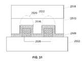
- FIG. 28is a diagram illustrating a cross-sectional view of the layers illustrated in FIG. 30 along the line AA′.
- FIG. 29is a diagram illustrating a cross-sectional view of the layers illustrated in FIG. 30 along the line BB′. Accordingly, it can be seen that bit lines 2506 now comprised channel regions 2516 under word line layer 2510 . The source and drain regions 2514 are then formed on either side of word lines 2510 . It will be understood, that formation of source/drain regions 2514 is a self-aligned process.
- an interlayer, or inter-module dielectric layer 2518can then be formed over word line layer 2510 .
- Another bit line and word line layercan then be formed on top of interlayer, or inter-module dielectric 2518 using the same processing steps as described above. In this manner, any number of word line and bit line layers, separated by an interlayer, or inter-module dielectric 2518 can be formed over insulating layer 2502 .
- memory cells 2520 - 2526can then be formed in the structure illustrated.
- Memory cells 2520 and 2522are illustrated in FIG. 31 as well.
- the source and drain regions for the memory cellsare formed from source/drain regions 2514 on either side of the associated word lines 2510 .
- the channel regionis formed from the regions 2516 of bit lines 2506 under word lines 2510 .
- Tri-gate devicescan exhibit excessive corner effect, but can also have increase cell current due to increased device width.
Landscapes
- Non-Volatile Memory (AREA)
- Semiconductor Memories (AREA)
Abstract
Description
This application claims the benefit of U.S. Provisional Application Ser. No. 60/748,911, entitled “The Process of TFT NAND and Nitride Read Only Memory,” filed Dec. 9, 2005, which is incorporated herein by reference as if set forth in full. This application is also related to U.S. patent application Ser. No. 11/425,959, entitled “A Stacked Non-Volatile Memory Device and Methods for Fabricating the Same,” Filed Jun. 22, 2006, and which is also incorporated herein by reference as if set forth in full.
1. Field of the Invention
The embodiments described herein are directed to methods for fabricating a thin film transistor, non-volatile memory devices, and more particularly to methods for fabricating a thin film transistor, non-volatile memory device comprising multiple layers of memory cells.
2. Background of the Invention
Non-volatile memory devices are finding uses in more and more products. For example, flash-based memory devices are being used in MP3 players, digital cameras, as storage devices for computer files, etc. As these uses grow, there is a need for larger memories housed in smaller packages. This requires the fabrication of highly dense memories. Accordingly, research and development has been directed at increasing the density of conventional non-volatile memory devices.
One approach for increasing the density of non-volatile memory devices is to create a stacked memory device, i.e., a device in which layers of memory cells are stacked on top of each other. Unfortunately, to date little effort has been put into creating certain types of stacked memory devices. For example, there are few stacked nitride read-only memory designs. This is in part because stacked memory devices are not necessarily compatible with the latest fabrication processes, which can make fabricating a stacked memory device inefficient and costly.
There are other approaches to increasing the density of conventional non-volatile memory devices; however, these approaches do not necessarily address the needs of all applications. Accordingly, there is still a need for further, or other approaches for increasing the density of conventional non-volatile memory devices.
One particular type of non-volatile memory device is the nitride read-only memory device.FIG. 1 is a diagram illustrating a conventional nitride read-only memory structure 150. As can be seen, nitride read-only memory 150 is constructed on asilicon substrate 152. The silicon substrate can be a P-type silicon substrate or an N-type silicon substrate; however, for various design reasons P-type silicon substrates are often preferred. Source/drain regions substrate 152. Atrapping structure 158 is then formed onsubstrate 152 between source/drain regions Control gate 160 is then formed on top oftrapping layer 158.
Source/drain regions substrate 152. For example, where a P-type silicon substrate 152 is used, N-type source/drain regions
Charge can be accumulated and confined withintrapping structure 158 next to source/drain regions independent charges charge
Each storage area in nitride read-only memory cell 150 can be programmed independently of the other storage area. A nitride read-only memory cell is programmed by applying a voltage that causes negatively charged electrons to be injected into the nitride layer oftrapping structure 158 near one end of the cell. Erasing is accomplished by applying voltages that cause holes to be injected into the nitride layer where they can compensate for electrons previously stored in the nitride layer during programming.
A nitride read only memory device is constructed by manufacturing arrays of memory cells such as the cell illustrated inFIG. 1 . Arrays are constructed by tying the cells together via word and bit lines. The bit lines are often polysilicon lines, while the word lines can be polysilicon or metal.
While nitride read-only memory devices, such as the device illustrated inFIG. 1 , can be configured to store multiple bits per cell, the density of nitride read-only memory devices can be increased by using a stacked construction. Unfortunately, the stacking of nitride read-only memory devices is rarely done and when it is, the process can be inefficient and therefore more costly.
Methods for fabricating a stacked non-volatile memory device is disclosed. The methods disclosed use efficient processing techniques in order to fabricate a stacked device. Accordingly, the embodiments described herein can be scaled to achieve various levels of stacking.
In one aspect, a stacked nitride read-only memory can be fabricated using the methods described herein.
In another aspect, the stacked nitride read-only memory device can comprise thin film transistors (TFTs) fabricated using Silicon On Insulator (SOI) processing techniques.
In another aspect, a trapping layer included in the stacked non-volatile memory device can include one of a plurality of structures such as a SONOS, BE-SONOS, SONS, an Hi-K material, to name just a few.
In another aspect, a stacked memory device fabricated using the methods described herein can be configured for NAND operation.
These and other features, aspects, and embodiments of the invention are described below in the section entitled “Detailed Description.”
Features, aspects, and embodiments of the inventions are described in conjunction with the attached drawings, in which:
It will be understood that any dimensions, measurements, ranges, test results, numerical data, etc., presented below are approximate in nature and unless otherwise stated not intended as precise data. The nature of the approximation involved will depend on the nature of the data, the context, and the specific embodiments or implementations being discussed.
Successive bitline layers and wordline layers can then be fabricated on insulatinglayer 102. For example, inFIG. 2 afirst bitline layer 110 is fabricated on insulatinglayer 102. Afirst wordline layer 120 is then fabricated on top offirst bit layer 110. Asecond bitline layer 130 is then fabricated on top offirst wordline layer 120. Finally, asecond wordline layer 140 is fabricated on top ofsecond bitline layer 130.
Further bitline and wordline layers can be successively fabricated on top of the layers illustrated inFIG. 1 . Thus, two bitline layers and two wordline layers are shown for convenience only and the methods described herein should not be seen as limited to a certain number of bitline layers and/or wordline layers. Eachbitline layer wordline layer
By using the stacked configuration illustrated inFIG. 2 , greater memory densities can be achieved. Further, as explained below, efficient processing techniques can be used to fabricatestructure 100.
As illustrated inFIG. 4 , conventional photolithography techniques can be used to pattern andetch layers FIG. 5 is a diagram illustrating a top view of the layers comprising the device as fabricated to this point.FIG. 4 is a cross sectional view ofFIG. 5 along the line AA′. Thus, as can be seen inFIG. 5 ,layer regions 205 that traverse insulatinglayer 202 from top to bottom. As will be explained below,regions 205 will form the bit lines of firstbit line layer 110 shown inFIG. 2 .
Referring toFIG. 6 , adielectric layer 209 can then be formed overinsulating layer 202 as illustrated.Dielectric layer 209 can be, for example, an oxide, such as a silicon dioxide (SiO2) layer and can be formed using High Density Plasma (HDP)—Chemical Vapor Deposition (CVD). Referring toFIG. 7 , a portion ofdielectric layer 209 is removed to expose the remaining portions ofcap layer 206 and part of the remaining portions ofsemiconductor layer 204. For example, a conventional wet etching, i.e., isotropic, process can be used to remove a portion ofdielectric layer 209. Removing the right amount ofdielectric layer 209 can be achieved by having a high etching selectivity ratio betweendielectric layer 209 andcap layer 206. The etching process producesdielectric regions 210 on top ofcap layer 206 as well asdielectric regions 212 in between the remaining portions ofsemiconductor layer 204.
Referring toFIG. 9 , the remaining portions ofcap layer 206 can be removed, removingregions 210 ofdielectric layer 209 in the process. For example, a hot phosphoric acid can be used to remove the remaining portions ofcap layer 206.Regions 210 ofdielectric layer 209 will automatically be removed during the removal of the remaining portions ofcap layer 206, becauseportions 210 are disconnected fromdielectric regions 212.
The process illustrated inFIGS. 6-9 are described in U.S. Pat. No. 6,380,068, entitled “Method for Planarizing a Flash Memory Device,” assigned to the assignee of the present application, issued Apr. 30, 2002, and incorporated herein by references as if set forth in full. The process described inFIGS. 6-9 result in an efficient planarization of the remaining surfaces illustrated inFIG. 9 . Accordingly, the fabrication processes described herein are compatible with newer, efficient processing techniques. This makes the fabrication of stacked non-volatile memory device efficient and cost-effective.
As illustrated inFIG. 11 , a trappingstructure 216 can then be formed over the remaining portions ofsemiconductor layer 204 and insulatingregions 212. A wordline conductor layer 218 can then be formed over trappingstructure 216. A SiN layer (not shown) can then be formed overlayer 218. The SiN layer (not shown) and layers218 and216 can then be patterned and etched using conventional photolithography techniques. The etching can be performed such thatHDP oxide regions 212 act as a stop for the etching process. Another HDP oxide layer can then be formed over the etched layers, including the SiN layer (not shown). The HDP layer can then be partially etched and then part of the HDP oxide layer can be removed along with the remaining SiN layer (not shown) in a manner similar as that illustrated inFIGS. 6-9 , to formword lines 219 illustrated inFIG. 12 .
In the example ofFIG. 11 , trappingstructure 216 can comprise a multi-layered structure. Examples of multi-layered structures are described more fully below with respect toFIGS. 18A-18H . Thus, trappingstructure 216 can be formed by sequentially forming the layers comprising trappingstructure 216.
Wordline conductor layer 218 can be formed from an N+ or P+ conductor material, such as a polysilicon material, polysilicon/silicide/polysilicon material, or a metal such as aluminum (Al), copper (Cu), or Tungsten (W).
As illustrated inFIG. 15 , oncewordlines 219 are formed overbit lines 205, source and drainregions 220 can be formed in the areas ofsemiconductor layer 204 comprisingbit lines 205 that are not covered byword line conductors 218. Accordingly, source and drainregions 220 can be implanted and heat-driven in theregions 220 ofsemiconductor layer 204. As will be understood, the process of implanting source and drainregions 220 is a self-aligned process. In the example ofFIG. 15 , the source and drain regions should be N+ regions formed using, e.g., arsenic (As), or phosphorous (P), sincesemiconductor layer 204 comprises P-type semiconductor material. It will be understood that P+ regions should be formed in embodiments that use N-type semiconductor material.
After formation of source and drainregions 220,semiconductor layer 204 will comprise source/drain regions 220 which are N+ region, and P-type regions underword line conductor 218. As explained below, these P-type regions will form the channel regions for particular memory cells.
The layers formed thus far will then form non-volatile memory cells240-256. The source and drain regions for non-volatile memory cells240-256 are formed from the N+ source/drain regions 220 on either side of the associatedwordlines 219. Referring toFIG. 13 , theareas 221 ofpolysilicon layer 204 formingbit lines 205 underwordlines 219 form the channel regions for non-volatile memory cells240-256. Trappingstructure 216 above these channel regions are used to store charge in each of cells240-256. The charge trapping structures are described more fully below with respect toFIGS. 18A-18H .
Accordingly, by applying the correct voltages toword line conductors 218 and source/drain regions 220, charge can be stored in trappingstructure 216 of the appropriate cells240-256. Similarly, cells240-256 can be erased by applying the appropriate voltages toword line conductors 218 and the associated source/drain regions 220. The programming status of cells240-256 can also be read by applying the appropriate voltages to the appropriateword line conductors 218 and source/drain regions 220.
As illustrated inFIG. 17 , additional memory cells260-270 can be formed by forming additional bit line and word line layers over bit line and word line layers210 and220 respectively. Thus, anadditional trapping structure 222 can be formed overword line conductor 218, and then an additionalbit line layer 230 can be formed on trappingstructure 222.Bit line layer 230 can be formed using the same steps illustrated above for formingbit line layer 210. Accordingly,bit line layer 230 will comprise the remaining portions of an etchedpolysilicon layer 224, wherein the remaining portions are separated bydielectric regions 226. The remaining portions ofpolysilicon layer 224 illustrated inFIG. 17 , which reside under the wordlines ofword line layer 240, can form the channel regions for additional cells260-270.
Source and drain regions can be implanted into the remaining portions ofpolysilicon layer 224, that reside on either side of the word lines ofword line layer 240.
Because of the efficient processing techniques used to form the word line and bit line layers, the process can be scaled to accommodate any number of layers. Thus, it will be understood that two bit line, and two word line layers are illustrated inFIG. 17 by way of convenience only.
NAND devices constructed using the SONOS trapping structure illustrated inFIG. 18A , can exhibit somewhat poorer charge retention due to leakage current that results from the direct tunneling of holes intotrapping layer 274 during charge retention.
In other embodiments, the trapping structure can comprise a SiN or a SiON, or a Hi-K material such as HfO2, Al2O3, AlN, etc. In general, any trapping structure or material can be used as long as it meets the requirements of a particular application.
Referring toFIG. 22 ,polysilicon layer 2504 can then be patterned and etched using conventional photolithography processes in order to producebit line regions 2506. For example, insulatinglayer 2502 can be used as an etch stop for the etching process in order to produceregions 2506. The overall thickness of the layers illustrated inFIG. 22 can be between approximately 200-1000 Å, and can prefer with the approximately 400 Å.
Referring toFIG. 23C , afterlayers regions cap layer 2508,regions 2510 can be removed using conventional processes.
Referring toFIG. 24 , a trappingstructure layer 2508 can be formed overinsulating layer 2502 and bitline regions 2506. As described above, trappingstructure layer 2508 can comprise any of a plurality of trapping structures, such as SONOS, BE-SONOS, top BE-SONOS, SONONS, SONOSLS, SLSLNLS, etc. In other embodiments, trappingstructure layer 2508 can comprise a SiN material, SiON material, or a high-K material such as HfO2, Al2O3, AlN, etc.
Referring toFIG. 25 , aword line layer 2510 can then be formed over trappingstructure layer 2508. For example,word line layer 2510 can comprise a polysilicon material deposited over trappingstructure layer 2508.Layers FIG. 27 , this will produceword lines 2510 overbit lines 2506.
As can be seen inFIG. 26 , the etching process can be configured such that it etches through trappingstructure layer 2508 in the regions in between word lines2510. This can produceregions 2506 withregions 2512 of trappingstructure layer 2508 remaining on the sides ofregions 2506.
Referring toFIG. 30 , source anddrain regions 2514 can be deposited in the areas ofbit lines 2506 that are not under word lines2510. For example, if word lines2506 are formed from a P-type polysilicon material, then N-type source/drain regions 2514 can be implanted and heat driven into the regions ofbit lines 2506 that are not under word lines2510. Alternatively, if word lines2506 are formed from an N-type polysilicon material, then P-type source/drain regions can be implanted and heat driven intobit lines 2506.
Referring toFIG. 31 , an interlayer, orinter-module dielectric layer 2518 can then be formed overword line layer 2510. Another bit line and word line layer can then be formed on top of interlayer, or inter-module dielectric2518 using the same processing steps as described above. In this manner, any number of word line and bit line layers, separated by an interlayer, or inter-module dielectric2518 can be formed overinsulating layer 2502.
Referring toFIG. 30 , memory cells2520-2526 can then be formed in the structure illustrated.Memory cells FIG. 31 as well. The source and drain regions for the memory cells are formed from source/drain regions 2514 on either side of the associated word lines2510. The channel region is formed from theregions 2516 ofbit lines 2506 under word lines2510.
It will be understood that the cells illustrated inFIGS. 30 and 31 are tri-gate devices. Tri-gate devices can exhibit excessive corner effect, but can also have increase cell current due to increased device width.
While certain embodiments of the inventions have been described above, it will be understood that the embodiments described are by way of example only. Accordingly, the inventions should not be limited based on the described embodiments. Rather, the scope of the inventions described herein should only be limited in light of the claims that follow when taken in conjunction with the above description and accompanying drawings.
Claims (47)
1. A method for fabricating a non-volatile memory device comprising a plurality of bitline layers and a plurality of wordline layers sequentially formed on top of each other, the method comprising:
forming the plurality of bitline layers layer, wherein forming each bitline layer comprises:
forming a semiconductor layer on an insulator, and
patterning and etching the semiconductor layer to form a plurality of bitlines;
forming word line layers in the plurality of wordline layers over respective preceding ones of the plurality of bitline layers, wherein forming each wordline layer comprises:
sequentially forming a trapping structure and a conducting layer, and
patterning and etching the trapping structure and the conducting layer to form a plurality of wordlines; and
forming source/drain regions in regions of the plurality of bitlines not covered by the plurality of wordlines with active regions in the plurality of bit lines beneath the plurality of wordlines.
2. The method ofclaim 1 , wherein patterning and etching the semiconductor layer comprises:
forming a cap layer over the semiconductor layer;
etching the cap layer and the semiconductor layer to form bitline regions comprising remaining portions of the cap layer and the semiconductor layer;
forming a dielectric layer over the etched cap and semiconductor layers;
etching a portion of the dielectric layer to form dielectric region between the bitline regions and on top of the remaining portions of the cap layer; and
removing the remaining portions of the cap layer and removing the remaining portions of the dielectric layer on top of the cap layer.
3. The method ofclaim 2 , wherein the cap layer comprises a nitride layer.
4. The method ofclaim 2 , wherein the dielectric layer comprises silicon dioxide.
5. The method ofclaim 4 , wherein the silicon dioxide is deposited using high density plasma, chemical vapor deposition.
6. The method ofclaim 1 , wherein forming the trapping structure comprises forming a silicon-oxide-nitride-oxide-silicon (SONOS) structure.
7. The method ofclaim 1 , wherein forming the trapping structure comprises forming an oxide-nitride-oxide (ONO), nitride read only memory structure.
8. The method ofclaim 1 , wherein forming the trapping structure comprises forming a Band-gap Engineered (BE)-SONOS structure.
9. The method ofclaim 1 , wherein forming the trapping structure comprises forming a silicon-oxide-nitride-silicon (SONS) structure.
10. The method ofclaim 1 , wherein forming the trapping structure comprises forming a top BE-SONOS structure.
11. The method ofclaim 1 , wherein forming the trapping structure comprises forming a top silicon-oxide-nitride-oxide-silicon-oxide-silicon (SONOSOS) structure.
12. The method ofclaim 1 , wherein forming the trapping structure comprises forming a bottom SOSONOS structure.
13. The method ofclaim 1 , wherein forming the trapping structure comprises forming a silicon-oxide-nitride-oxide-nitride-silicon (SONONS) structure.
14. The method ofclaim 1 , wherein forming the trapping structure comprises forming a silicon nitride (SiN) layer.
15. The method ofclaim 1 , wherein forming the trapping structure comprises forming a SiON layer.
16. The method ofclaim 1 , wherein forming the trapping layer comprises depositing a Hi-K material.
17. The method ofclaim 16 , wherein the Hi-K material is HfO2, AlN, or Al2O3.
18. The method ofclaim 1 , wherein the semiconductor layer comprises a P-type semiconductor material, and wherein forming the source drain regions comprises forming N+ regions in the P-type semiconductor material.
19. The method ofclaim 18 , wherein the N+ regions are formed using As or P.
20. The method ofclaim 1 , wherein the conducting layer comprises polysilicon material.
21. The method ofclaim 1 , wherein the conducting layer comprises polysilicon/silicide/polysilicon material.
22. The method ofclaim 1 , wherein the conducting layer comprises a metal.
23. The method ofclaim 22 , wherein the metal is aluminum, copper, or tungsten.
24. The method ofclaim 1 , wherein patterning and etching the trapping structure and conducting layer comprises:
forming a cap layer over the trapping structure and conducting layer;
etching the cap layer and the trapping structure and conducting layer to form wordline regions comprising remaining portions of the cap layer and the trapping structure and conducting layer;
forming a dielectric layer over the etched cap and trapping structure and conducting layers;
etching a portion of the dielectric layer to form dielectric regions between the wordlines and on top of the remaining portions of the cap layer; and
removing the remaining portions of the cap layer and removing the portions of the dielectric layer on top of the cap layer.
25. The method ofclaim 24 , wherein the cap layer comprises a nitride layer.
26. The method ofclaim 24 , wherein the dielectric layer comprises silicon dioxide.
27. The method ofclaim 26 , wherein the silicon dioxide is deposited using high density plasma, chemical vapor deposition.
28. A method for fabricating a non-volatile memory device comprising a plurality of bitline layers and a plurality of wordline layers sequentially formed on top of each other, the method comprising:
forming the plurality of bitline layers, wherein forming each bitline layer comprises:
forming a first semiconductor layer on an insulator,
forming a cap layer over the semiconductor layer,
etching the cap layer and the first semiconductor layer to form bitline regions comprising remaining portions of the cap layer and the semiconductor layer,
forming a dielectric layer over the etched cap and semiconductor layers,
etching a portion of the dielectric layer to form dielectric regions between the bitline regions and dielectric regions on top of the remaining portions of the cap layer, and
removing the remaining portions of the cap layer and removing the remaining portions of the dielectric layer on top of the cap layer; and
forming the plurality of wordline layers over a preceding one of the plurality of bitline layers, wherein forming each wordline layer comprises:
sequentially forming a trapping structure and a conducting layer, the trapping structure comprising a multilayer structure, and
patterning and etching the trapping structure and the conducting layer to form a plurality of wordlines.
29. The method ofclaim 28 , wherein the cap layer comprises a nitride layer.
30. The method ofclaim 28 , wherein the dielectric layer comprises silicon dioxide.
31. The method ofclaim 30 , wherein the silicon dioxide is deposited using high density plasma, chemical vapor deposition.
32. The method ofclaim 28 , wherein forming the trapping structure comprises forming a silicon-oxide-nitride-oxide-silicon (SONOS) structure.
33. The method ofclaim 28 , wherein forming the trapping structure comprises forming an oxide-nitride-oxide (ONO), nitride read only memory structure.
34. The method ofclaim 28 , wherein forming the trapping structure comprises forming a Band-gap Engineered (BE)-SONOS structure.
35. The method ofclaim 28 , wherein forming the trapping structure comprises forming a silicon-oxide-nitride-silicon (SONS) structure.
36. The method ofclaim 28 , wherein forming the trapping structure comprises forming a top BE-SONOS structure.
37. The method ofclaim 28 , wherein forming the trapping structure comprises forming a top silicon-oxide-nitride-oxide-silicon-oxide-silicon (SONOSOS) structure.
38. The method ofclaim 28 , wherein forming the trapping structure comprises forming a bottom SOSONOS structure.
39. The method ofclaim 28 , wherein forming the trapping structure comprises forming a silicon-oxide-nitride-oxide-nitride-silicon (SONONS) structure.
40. The method ofclaim 28 , wherein forming the trapping structure comprises forming a silicon nitride (SiN) layer.
41. The method ofclaim 28 , wherein forming the trapping structure comprises forming a SiON layer.
42. The method ofclaim 28 , further comprising forming source/drain regions in the regions of the plurality of bitlines not covered by the plurality of wordlines.
43. The method ofclaim 42 , wherein the semiconductor layer comprises a P-type semiconductor material, and wherein forming the source drain regions comprises forming N+ regions in the P-type semiconductor material.
44. The method ofclaim 43 , wherein the N+ regions are formed using As or P.
45. The method ofclaim 28 , wherein the conducting layer comprises polysilicon material.
46. The method ofclaim 28 , wherein the conducting layer comprises polysilicon/silicide/polysilicon material.
47. The method ofclaim 28 , wherein the conducting layer comprises a metal.
Priority Applications (10)
| Application Number | Priority Date | Filing Date | Title |
|---|---|---|---|
| US11/549,520US7473589B2 (en) | 2005-12-09 | 2006-10-13 | Stacked thin film transistor, non-volatile memory devices and methods for fabricating the same |
| TW095146134ATWI336136B (en) | 2005-12-09 | 2006-12-08 | A stacked thin film transistor non-volatile memory devices and methods for fabricating the same |
| JP2007152454AJP2008098602A (en) | 2006-10-13 | 2007-06-08 | LAMINATED THIN FILM TRANSISTOR TYPE NONVOLATILE MEMORY DEVICE AND METHOD FOR MANUFACTURING THE SAME |
| AT07252422TATE533179T1 (en) | 2006-10-13 | 2007-06-14 | PRODUCTION METHOD FOR A NON-VOLATILE MEMORY COMPONENT |
| EP07252422AEP1912255B1 (en) | 2006-10-13 | 2007-06-14 | Method for fabricating a non-volatile memory device |
| KR1020070071511AKR100876851B1 (en) | 2006-10-13 | 2007-07-18 | Stacked thin film transistor nonvolatile memory device and method for manufacturing same |
| US12/056,489US8482052B2 (en) | 2005-01-03 | 2008-03-27 | Silicon on insulator and thin film transistor bandgap engineered split gate memory |
| US12/337,289US7999295B2 (en) | 2005-12-09 | 2008-12-17 | Stacked thin film transistor, non-volatile memory devices and methods for fabricating the same |
| US13/899,629US8937340B2 (en) | 2005-01-03 | 2013-05-22 | Silicon on insulator and thin film transistor bandgap engineered split gate memory |
| US15/210,751USRE47311E1 (en) | 2005-01-03 | 2016-07-14 | Silicon on insulator and thin film transistor bandgap engineered split gate memory |
Applications Claiming Priority (2)
| Application Number | Priority Date | Filing Date | Title |
|---|---|---|---|
| US74891105P | 2005-12-09 | 2005-12-09 | |
| US11/549,520US7473589B2 (en) | 2005-12-09 | 2006-10-13 | Stacked thin film transistor, non-volatile memory devices and methods for fabricating the same |
Related Parent Applications (1)
| Application Number | Title | Priority Date | Filing Date |
|---|---|---|---|
| US11/425,959Continuation-In-PartUS7709334B2 (en) | 2005-01-03 | 2006-06-22 | Stacked non-volatile memory device and methods for fabricating the same |
Related Child Applications (4)
| Application Number | Title | Priority Date | Filing Date |
|---|---|---|---|
| US11/425,959Continuation-In-PartUS7709334B2 (en) | 2005-01-03 | 2006-06-22 | Stacked non-volatile memory device and methods for fabricating the same |
| US11/831,594Continuation-In-PartUS7426140B2 (en) | 2005-01-03 | 2007-07-31 | Bandgap engineered split gate memory |
| US12/056,489Continuation-In-PartUS8482052B2 (en) | 2005-01-03 | 2008-03-27 | Silicon on insulator and thin film transistor bandgap engineered split gate memory |
| US12/337,289ContinuationUS7999295B2 (en) | 2005-12-09 | 2008-12-17 | Stacked thin film transistor, non-volatile memory devices and methods for fabricating the same |
Publications (2)
| Publication Number | Publication Date |
|---|---|
| US20070134876A1 US20070134876A1 (en) | 2007-06-14 |
| US7473589B2true US7473589B2 (en) | 2009-01-06 |
Family
ID=38473904
Family Applications (2)
| Application Number | Title | Priority Date | Filing Date |
|---|---|---|---|
| US11/549,520Active2026-11-29US7473589B2 (en) | 2005-01-03 | 2006-10-13 | Stacked thin film transistor, non-volatile memory devices and methods for fabricating the same |
| US12/337,289Active2027-10-06US7999295B2 (en) | 2005-12-09 | 2008-12-17 | Stacked thin film transistor, non-volatile memory devices and methods for fabricating the same |
Family Applications After (1)
| Application Number | Title | Priority Date | Filing Date |
|---|---|---|---|
| US12/337,289Active2027-10-06US7999295B2 (en) | 2005-12-09 | 2008-12-17 | Stacked thin film transistor, non-volatile memory devices and methods for fabricating the same |
Country Status (5)
| Country | Link |
|---|---|
| US (2) | US7473589B2 (en) |
| EP (1) | EP1912255B1 (en) |
| JP (1) | JP2008098602A (en) |
| KR (1) | KR100876851B1 (en) |
| AT (1) | ATE533179T1 (en) |
Cited By (26)
| Publication number | Priority date | Publication date | Assignee | Title |
|---|---|---|---|---|
| US20070138539A1 (en)* | 2005-12-15 | 2007-06-21 | Macronix International Co., Ltd. | Non-volatile memory device having a nitride-oxide dielectric layer |
| US20070268753A1 (en)* | 2005-01-03 | 2007-11-22 | Macronix International Co., Ltd. | Methods of operating bandgap engineered memory |
| US20090059676A1 (en)* | 2007-08-27 | 2009-03-05 | Macronix International Co., Ltd. | HIGH-k CAPPED BLOCKING DIELECTRIC BANDGAP ENGINEERED SONOS AND MONOS |
| US20090065851A1 (en)* | 2006-06-20 | 2009-03-12 | Macronix International Co., Ltd | Operating method of non-volatile memory device |
| US20090096017A1 (en)* | 2005-12-09 | 2009-04-16 | Macronix International Co., Ltd. | Stacked thin film transistor, non-volatile memory devices and methods for fabricating the same |
| US20090103370A1 (en)* | 2007-10-18 | 2009-04-23 | Macronix International Co., Ltd. | Efficient erase algorithm for sonos-type nand flash |
| US20090141555A1 (en)* | 2006-05-05 | 2009-06-04 | Macronix International Co., Ltd. | Method of programming and erasing a p-channel be-sonos nand flash memory |
| US20090262583A1 (en)* | 2008-04-18 | 2009-10-22 | Macronix International Co., Ltd. | Floating gate memory device with interpoly charge trapping structure |
| US20090288211A1 (en)* | 2008-05-15 | 2009-11-19 | Monsanto Technology Llc | Plants and seeds of hybrid corn variety ch408813 |
| US20100172183A1 (en)* | 2009-01-02 | 2010-07-08 | Macronix International Co., Ltd. | Method and Apparatus to Suppress Fringing Field Interference of Charge Trapping NAND Memory |
| US20100193859A1 (en)* | 2007-08-09 | 2010-08-05 | Macronix International Co., Ltd. | Blocking dielectric engineered charge trapping memory cell with high speed erase |
| US20100227466A1 (en)* | 2006-07-10 | 2010-09-09 | Macronix International Co., Ltd. | Nonvolatile Memory Array Having Modified Channel Region Interface |
| US20100265766A1 (en)* | 2009-04-21 | 2010-10-21 | Macronix International Co., Ltd. | Bandgap engineered charge trapping memory in two-transistor nor architecture |
| US8486791B2 (en) | 2011-01-19 | 2013-07-16 | Macronix International Co., Ltd. | Mufti-layer single crystal 3D stackable memory |
| US20150108619A1 (en)* | 2013-10-21 | 2015-04-23 | Applied Materials, Inc. | Method for patterning a semiconductor substrate |
| US9018692B2 (en) | 2011-01-19 | 2015-04-28 | Macronix International Co., Ltd. | Low cost scalable 3D memory |
| US9111597B2 (en) | 2012-12-20 | 2015-08-18 | Macronix International Co., Ltd. | Memory device structure with decoders in a device level separate from the array level |
| US9171636B2 (en) | 2013-01-29 | 2015-10-27 | Macronix International Co. Ltd. | Hot carrier generation and programming in NAND flash |
| US9214351B2 (en) | 2013-03-12 | 2015-12-15 | Macronix International Co., Ltd. | Memory architecture of thin film 3D array |
| US9224474B2 (en) | 2013-01-09 | 2015-12-29 | Macronix International Co., Ltd. | P-channel 3D memory array and methods to program and erase the same at bit level and block level utilizing band-to-band and fowler-nordheim tunneling principals |
| US9236392B1 (en)* | 2014-08-26 | 2016-01-12 | Sandisk Technologies Inc. | Multiheight electrically conductive via contacts for a multilevel interconnect structure |
| US9240405B2 (en) | 2011-04-19 | 2016-01-19 | Macronix International Co., Ltd. | Memory with off-chip controller |
| US9401309B2 (en) | 2014-08-26 | 2016-07-26 | Sandisk Technologies Llc | Multiheight contact via structures for a multilevel interconnect structure |
| US9559113B2 (en) | 2014-05-01 | 2017-01-31 | Macronix International Co., Ltd. | SSL/GSL gate oxide in 3D vertical channel NAND |
| US9601502B2 (en) | 2014-08-26 | 2017-03-21 | Sandisk Technologies Llc | Multiheight contact via structures for a multilevel interconnect structure |
| USRE47311E1 (en) | 2005-01-03 | 2019-03-19 | Macronix International Co., Ltd. | Silicon on insulator and thin film transistor bandgap engineered split gate memory |
Families Citing this family (48)
| Publication number | Priority date | Publication date | Assignee | Title |
|---|---|---|---|---|
| US9449831B2 (en) | 2007-05-25 | 2016-09-20 | Cypress Semiconductor Corporation | Oxide-nitride-oxide stack having multiple oxynitride layers |
| US8614124B2 (en) | 2007-05-25 | 2013-12-24 | Cypress Semiconductor Corporation | SONOS ONO stack scaling |
| US8940645B2 (en) | 2007-05-25 | 2015-01-27 | Cypress Semiconductor Corporation | Radical oxidation process for fabricating a nonvolatile charge trap memory device |
| US8283261B2 (en) | 2007-05-25 | 2012-10-09 | Cypress Semiconductor Corporation | Radical oxidation process for fabricating a nonvolatile charge trap memory device |
| US9299568B2 (en) | 2007-05-25 | 2016-03-29 | Cypress Semiconductor Corporation | SONOS ONO stack scaling |
| US20090179253A1 (en) | 2007-05-25 | 2009-07-16 | Cypress Semiconductor Corporation | Oxide-nitride-oxide stack having multiple oxynitride layers |
| US8093128B2 (en)* | 2007-05-25 | 2012-01-10 | Cypress Semiconductor Corporation | Integration of non-volatile charge trap memory devices and logic CMOS devices |
| US8680601B2 (en) | 2007-05-25 | 2014-03-25 | Cypress Semiconductor Corporation | Nonvolatile charge trap memory device having a deuterated layer in a multi-layer charge-trapping region |
| US8643124B2 (en) | 2007-05-25 | 2014-02-04 | Cypress Semiconductor Corporation | Oxide-nitride-oxide stack having multiple oxynitride layers |
| US8871595B2 (en) | 2007-05-25 | 2014-10-28 | Cypress Semiconductor Corporation | Integration of non-volatile charge trap memory devices and logic CMOS devices |
| US8633537B2 (en) | 2007-05-25 | 2014-01-21 | Cypress Semiconductor Corporation | Memory transistor with multiple charge storing layers and a high work function gate electrode |
| US8063434B1 (en) | 2007-05-25 | 2011-11-22 | Cypress Semiconductor Corporation | Memory transistor with multiple charge storing layers and a high work function gate electrode |
| US9716153B2 (en) | 2007-05-25 | 2017-07-25 | Cypress Semiconductor Corporation | Nonvolatile charge trap memory device having a deuterated layer in a multi-layer charge-trapping region |
| US20080315206A1 (en)* | 2007-06-19 | 2008-12-25 | Herner S Brad | Highly Scalable Thin Film Transistor |
| EP2026384A3 (en)* | 2007-08-13 | 2009-06-10 | Macronix International Co., Ltd. | Charge trapping memory cell with high speed erase |
| US8320191B2 (en) | 2007-08-30 | 2012-11-27 | Infineon Technologies Ag | Memory cell arrangement, method for controlling a memory cell, memory array and electronic device |
| US7848148B2 (en)* | 2007-10-18 | 2010-12-07 | Macronix International Co., Ltd. | One-transistor cell semiconductor on insulator random access memory |
| US9431549B2 (en) | 2007-12-12 | 2016-08-30 | Cypress Semiconductor Corporation | Nonvolatile charge trap memory device having a high dielectric constant blocking region |
| US8148763B2 (en) | 2008-11-25 | 2012-04-03 | Samsung Electronics Co., Ltd. | Three-dimensional semiconductor devices |
| US8222688B1 (en) | 2009-04-24 | 2012-07-17 | Cypress Semiconductor Corporation | SONOS stack with split nitride memory layer |
| US8710578B2 (en) | 2009-04-24 | 2014-04-29 | Cypress Semiconductor Corporation | SONOS stack with split nitride memory layer |
| US8569829B2 (en) | 2009-12-28 | 2013-10-29 | Kabushiki Kaisha Toshiba | Nonvolatile semiconductor memory device |
| US8355281B2 (en)* | 2010-04-20 | 2013-01-15 | Micron Technology, Inc. | Flash memory having multi-level architecture |
| US8501609B2 (en) | 2012-02-02 | 2013-08-06 | Tower Semiconductor Ltd. | Method for generating a three-dimensional NAND memory with mono-crystalline channels using sacrificial material |
| US8599616B2 (en) | 2012-02-02 | 2013-12-03 | Tower Semiconductor Ltd. | Three-dimensional NAND memory with stacked mono-crystalline channels |
| US8685813B2 (en) | 2012-02-15 | 2014-04-01 | Cypress Semiconductor Corporation | Method of integrating a charge-trapping gate stack into a CMOS flow |
| CN104254921B (en)* | 2012-03-27 | 2020-06-12 | 经度快闪存储解决方案有限责任公司 | SONOS stack with separated nitride storage layer |
| EP3229276A1 (en)* | 2012-03-31 | 2017-10-11 | Cypress Semiconductor Corporation | Integration of non-volatile charge trap memory devices and logic cmos devices |
| KR102078611B1 (en)* | 2012-07-01 | 2020-04-08 | 롱지튜드 플래쉬 메모리 솔루션즈 리미티드 | Memory transistor with multiple charge storing layers |
| KR102115156B1 (en)* | 2012-07-01 | 2020-05-27 | 사이프레스 세미컨덕터 코포레이션 | Nonvolatile charge trap memory device having a deuterated layer in a multy-layer charge-trapping region |
| US11120884B2 (en) | 2015-09-30 | 2021-09-14 | Sunrise Memory Corporation | Implementing logic function and generating analog signals using NOR memory strings |
| US9892800B2 (en) | 2015-09-30 | 2018-02-13 | Sunrise Memory Corporation | Multi-gate NOR flash thin-film transistor strings arranged in stacked horizontal active strips with vertical control gates |
| US10121553B2 (en) | 2015-09-30 | 2018-11-06 | Sunrise Memory Corporation | Capacitive-coupled non-volatile thin-film transistor NOR strings in three-dimensional arrays |
| US9842651B2 (en) | 2015-11-25 | 2017-12-12 | Sunrise Memory Corporation | Three-dimensional vertical NOR flash thin film transistor strings |
| US10608008B2 (en) | 2017-06-20 | 2020-03-31 | Sunrise Memory Corporation | 3-dimensional nor strings with segmented shared source regions |
| US10692874B2 (en) | 2017-06-20 | 2020-06-23 | Sunrise Memory Corporation | 3-dimensional NOR string arrays in segmented stacks |
| KR102719982B1 (en) | 2017-06-20 | 2024-10-22 | 선라이즈 메모리 코포레이션 | 3D NOR memory array architecture and its manufacturing method |
| US10475812B2 (en) | 2018-02-02 | 2019-11-12 | Sunrise Memory Corporation | Three-dimensional vertical NOR flash thin-film transistor strings |
| US11069696B2 (en) | 2018-07-12 | 2021-07-20 | Sunrise Memory Corporation | Device structure for a 3-dimensional NOR memory array and methods for improved erase operations applied thereto |
| EP3891780A4 (en) | 2018-12-07 | 2022-12-21 | Sunrise Memory Corporation | METHOD OF FABRICATION OF MULTILAYER VERTICAL NOR STORAGE STRING ARRAYS |
| WO2021127218A1 (en) | 2019-12-19 | 2021-06-24 | Sunrise Memory Corporation | Process for preparing a channel region of a thin-film transistor |
| TWI767512B (en) | 2020-01-22 | 2022-06-11 | 美商森恩萊斯記憶體公司 | Cool electron erasing in thin-film storage transistors |
| TWI836184B (en) | 2020-02-07 | 2024-03-21 | 美商森恩萊斯記憶體公司 | High capacity memory circuit with low effective latency |
| US11705496B2 (en) | 2020-04-08 | 2023-07-18 | Sunrise Memory Corporation | Charge-trapping layer with optimized number of charge-trapping sites for fast program and erase of a memory cell in a 3-dimensional NOR memory string array |
| WO2022108848A1 (en) | 2020-11-17 | 2022-05-27 | Sunrise Memory Corporation | Methods for reducing disturb errors by refreshing data alongside programming or erase operations |
| US11848056B2 (en) | 2020-12-08 | 2023-12-19 | Sunrise Memory Corporation | Quasi-volatile memory with enhanced sense amplifier operation |
| TW202310429A (en) | 2021-07-16 | 2023-03-01 | 美商日升存儲公司 | 3-dimensional memory string array of thin-film ferroelectric transistors |
| US12402319B2 (en) | 2021-09-14 | 2025-08-26 | Sunrise Memory Corporation | Three-dimensional memory string array of thin-film ferroelectric transistors formed with an oxide semiconductor channel |
Citations (188)
| Publication number | Priority date | Publication date | Assignee | Title |
|---|---|---|---|---|
| EP0016246B1 (en) | 1979-02-15 | 1983-01-19 | International Business Machines Corporation | Semiconductor field effect structure of the metal-insulator-metal or metal-insulator-semiconductor type, and memory device comprising such structure |
| US4630086A (en) | 1982-09-24 | 1986-12-16 | Hitachi, Ltd. | Nonvolatile MNOS memory |
| US4959812A (en) | 1987-12-28 | 1990-09-25 | Kabushiki Kaisha Toshiba | Electrically erasable programmable read-only memory with NAND cell structure |
| US5270969A (en) | 1987-06-29 | 1993-12-14 | Kabushiki Kaisha Toshiba | Electrically programmable nonvolatile semiconductor memory device with nand cell structure |
| US5278439A (en) | 1991-08-29 | 1994-01-11 | Ma Yueh Y | Self-aligned dual-bit split gate (DSG) flash EEPROM cell |
| US5286994A (en) | 1991-08-22 | 1994-02-15 | Rohm Co., Ltd. | Semiconductor memory trap film assembly having plural laminated gate insulating films |
| US5319229A (en) | 1991-08-22 | 1994-06-07 | Noriyuki Shimoji | Semiconductor nonvolatile memory with wide memory window and long data retention time |
| US5338952A (en) | 1991-06-07 | 1994-08-16 | Sharp Kabushiki Kaisha | Non-volatile memory |
| US5355464A (en) | 1991-02-11 | 1994-10-11 | Intel Corporation | Circuitry and method for suspending the automated erasure of a non-volatile semiconductor memory |
| WO1994028551A1 (en) | 1993-05-28 | 1994-12-08 | Macronix International Co., Ltd. | Flash eprom with block erase flags for over-erase protection |
| US5408115A (en) | 1994-04-04 | 1995-04-18 | Motorola Inc. | Self-aligned, split-gate EEPROM device |
| US5412603A (en) | 1994-05-06 | 1995-05-02 | Texas Instruments Incorporated | Method and circuitry for programming floating-gate memory cell using a single low-voltage supply |
| US5424569A (en) | 1994-05-05 | 1995-06-13 | Micron Technology, Inc. | Array of non-volatile sonos memory cells |
| US5448517A (en) | 1987-06-29 | 1995-09-05 | Kabushiki Kaisha Toshiba | Electrically programmable nonvolatile semiconductor memory device with NAND cell structure |
| US5483486A (en) | 1994-10-19 | 1996-01-09 | Intel Corporation | Charge pump circuit for providing multiple output voltages for flash memory |
| US5485422A (en) | 1994-06-02 | 1996-01-16 | Intel Corporation | Drain bias multiplexing for multiple bit flash cell |
| US5509134A (en) | 1993-06-30 | 1996-04-16 | Intel Corporation | Method and apparatus for execution of operations in a flash memory array |
| US5515324A (en) | 1993-09-17 | 1996-05-07 | Kabushiki Kaisha Toshiba | EEPROM having NAND type memory cell array |
| US5566120A (en) | 1995-10-19 | 1996-10-15 | Sun Microsystems, Inc. | Apparatus and method for controlling transistor current leakage |
| US5602775A (en) | 1995-03-15 | 1997-02-11 | National Semiconductor Corporation | Flash EEPROM Memory system for low voltage operation and method |
| JPH09162313A (en) | 1995-12-12 | 1997-06-20 | Rohm Co Ltd | Nonvolatile semiconductor memory device and method of using the same |
| US5644533A (en) | 1992-11-02 | 1997-07-01 | Nvx Corporation | Flash memory system, and methods of constructing and utilizing same |
| US5668029A (en)* | 1996-05-06 | 1997-09-16 | United Microelectronics Corporation | Process for fabricating multi-level read-only memory device |
| US5694356A (en) | 1994-11-02 | 1997-12-02 | Invoice Technology, Inc. | High resolution analog storage EPROM and flash EPROM |
| US5745410A (en) | 1995-11-17 | 1998-04-28 | Macronix International Co., Ltd. | Method and system for soft programming algorithm |
| US5753950A (en) | 1995-05-19 | 1998-05-19 | Motorola, Inc. | Non-volatile memory having a cell applying to multi-bit data by double layered floating gate architecture and programming/erasing/reading method for the same |
| US5768192A (en) | 1996-07-23 | 1998-06-16 | Saifun Semiconductors, Ltd. | Non-volatile semiconductor memory cell utilizing asymmetrical charge trapping |
| USRE35838E (en) | 1987-12-28 | 1998-07-07 | Kabushiki Kaisha Toshiba | Electrically erasable programmable read-only memory with NAND cell structure |
| US5793677A (en) | 1996-06-18 | 1998-08-11 | Hu; Chung-You | Using floating gate devices as select gate devices for NAND flash memory and its bias scheme |
| US5835396A (en)* | 1996-10-17 | 1998-11-10 | Zhang; Guobiao | Three-dimensional read-only memory |
| JPH1140682A (en) | 1997-07-18 | 1999-02-12 | Sony Corp | Non-volatile semiconductor memory and its manufacture |
| US5877054A (en) | 1995-06-29 | 1999-03-02 | Sharp Kabushiki Kaisha | Method of making nonvolatile semiconductor memory |
| US5883409A (en)* | 1992-01-14 | 1999-03-16 | Sandisk Corporation | EEPROM with split gate source side injection |
| US5895949A (en) | 1993-06-29 | 1999-04-20 | Kabushiki Kaisha Toshiba | Semiconductor device having inversion inducing gate |
| JPH11233653A (en) | 1998-02-13 | 1999-08-27 | Sony Corp | Deletion method for nonvolatile semiconductor storage device |
| US5952692A (en) | 1996-11-15 | 1999-09-14 | Hitachi, Ltd. | Memory device with improved charge storage barrier structure |
| US5966603A (en) | 1997-06-11 | 1999-10-12 | Saifun Semiconductors Ltd. | NROM fabrication method with a periphery portion |
| US6011725A (en) | 1997-08-01 | 2000-01-04 | Saifun Semiconductors, Ltd. | Two bit non-volatile electrically erasable and programmable semiconductor memory cell utilizing asymmetrical charge trapping |
| US6026026A (en) | 1997-12-05 | 2000-02-15 | Hyundai Electronics America, Inc. | Self-convergence of post-erase threshold voltages in a flash memory cell using transient response |
| US6034896A (en) | 1995-07-03 | 2000-03-07 | The University Of Toronto, Innovations Foundation | Method of fabricating a fast programmable flash E2 PROM cell |
| US6074917A (en) | 1998-06-16 | 2000-06-13 | Advanced Micro Devices, Inc. | LPCVD oxide and RTA for top oxide of ONO film to improve reliability for flash memory devices |
| US6096603A (en) | 1998-02-16 | 2000-08-01 | Worldwide Semiconductor Manufacturing Corp. | Method of fabricating a split gate structure of a flash memory |
| US6103572A (en) | 1997-02-07 | 2000-08-15 | Citizen Watch Co., Ltd. | Method of fabricating a semiconductor nonvolatile storage device |
| US6151248A (en) | 1999-06-30 | 2000-11-21 | Sandisk Corporation | Dual floating gate EEPROM cell array with steering gates shared by adjacent cells |
| US6172907B1 (en) | 1999-10-22 | 2001-01-09 | Cypress Semiconductor Corporation | Silicon-oxide-nitride-oxide-semiconductor (SONOS) type memory cell and method for retaining data in the same |
| US6194272B1 (en) | 1998-05-19 | 2001-02-27 | Mosel Vitelic, Inc. | Split gate flash cell with extremely small cell size |
| US6215148B1 (en) | 1998-05-20 | 2001-04-10 | Saifun Semiconductors Ltd. | NROM cell with improved programming, erasing and cycling |
| US6219276B1 (en) | 2000-02-25 | 2001-04-17 | Advanced Micro Devices, Inc. | Multilevel cell programming |
| US6218700B1 (en) | 1997-10-29 | 2001-04-17 | Stmicroelectronics S.A. | Remanent memory device |
| WO2001037347A1 (en) | 1999-11-18 | 2001-05-25 | Infineon Technologies Ag | Non-volatile semiconductor memory location and method for producing the same |
| US20010012663A1 (en) | 1995-10-30 | 2001-08-09 | Angelo Magri' | Single feature size mos technology power device |
| US6289175B1 (en) | 1999-02-17 | 2001-09-11 | De'longhi S.P.A. | Independently operating portable radiator |
| US6297096B1 (en) | 1997-06-11 | 2001-10-02 | Saifun Semiconductors Ltd. | NROM fabrication method |
| US6320786B1 (en) | 2000-12-22 | 2001-11-20 | Macronix International Co., Ltd. | Method of controlling multi-state NROM |
| US6322903B1 (en)* | 1999-12-06 | 2001-11-27 | Tru-Si Technologies, Inc. | Package of integrated circuits and vertical integration |
| US20010045615A1 (en) | 1997-01-16 | 2001-11-29 | International Rectifier Corporation | High band gap layer to isolate wells in high voltage power integrated circuits |
| US20010055838A1 (en)* | 2000-04-28 | 2001-12-27 | Matrix Semiconductor Inc. | Nonvolatile memory on SOI and compound semiconductor substrates and method of fabrication |
| US6356478B1 (en) | 2000-12-21 | 2002-03-12 | Actel Corporation | Flash based control for field programmable gate array |
| US6363013B1 (en) | 2000-08-29 | 2002-03-26 | Macronix International Co., Ltd. | Auto-stopped page soft-programming method with voltage limited component |
| US6396741B1 (en) | 2000-05-04 | 2002-05-28 | Saifun Semiconductors Ltd. | Programming of nonvolatile memory cells |
| US6436768B1 (en) | 2001-06-27 | 2002-08-20 | Advanced Micro Devices, Inc. | Source drain implant during ONO formation for improved isolation of SONOS devices |
| US6458642B1 (en) | 2001-10-29 | 2002-10-01 | Macronix International Co., Ltd. | Method of fabricating a sonos device |
| US20020167844A1 (en) | 2001-05-14 | 2002-11-14 | Han Kyung Joon | Method and apparatus for multiple byte or page mode programming and reading and for erasing of a flash memory array |
| US6487114B2 (en) | 2001-02-28 | 2002-11-26 | Macronix International Co., Ltd. | Method of reading two-bit memories of NROM cell |
| US20020179958A1 (en) | 2001-06-02 | 2002-12-05 | Kim Dae Mann | SONOS flash cells for embedded memory logic, free of drain turn-on and over-erase |
| JP2002368141A (en) | 2001-06-06 | 2002-12-20 | Sony Corp | Nonvolatile semiconductor memory device |
| US6512696B1 (en) | 2001-11-13 | 2003-01-28 | Macronix International Co., Ltd. | Method of programming and erasing a SNNNS type non-volatile memory cell |
| US20030023603A1 (en) | 1999-01-29 | 2003-01-30 | Ellison Lawrence J. | Database server with enhanced management and self-configuration features |
| US20030025147A1 (en) | 2001-07-19 | 2003-02-06 | Kazumasa Nomoto | Semiconductor device and method of producing the same |
| US20030032242A1 (en) | 2001-08-09 | 2003-02-13 | Samsung Electronics Co., Ltd. | Method of forming non-volatile memory having floating trap type device |
| US20030030100A1 (en) | 2001-07-31 | 2003-02-13 | Samsung Electronics Co., Ltd. | Non-volatile memory device and method for fabricating the same |
| US6522585B2 (en) | 2001-05-25 | 2003-02-18 | Sandisk Corporation | Dual-cell soft programming for virtual-ground memory arrays |
| US20030036250A1 (en) | 2001-08-07 | 2003-02-20 | Hung-Sui Lin | Operation method for programming and erasing a data in a P-channel sonos memory cell |
| US20030042534A1 (en) | 2001-08-30 | 2003-03-06 | Micron Technology, Inc. | Scalable flash/NV structures and devices with extended endurance |
| US20030047755A1 (en) | 2001-06-28 | 2003-03-13 | Chang-Hyun Lee | Floating trap non-volatile semiconductor memory devices including high dielectric constant blocking insulating layers and methods |
| US6538923B1 (en) | 2001-02-26 | 2003-03-25 | Advanced Micro Devices, Inc. | Staircase program verify for multi-level cell flash memory designs |
| US20030067032A1 (en) | 2001-10-08 | 2003-04-10 | Stmicroelectronics S.R.I. | Process for manufacturing a dual charge storage location memory cell |
| US6552386B1 (en) | 2002-09-30 | 2003-04-22 | Silicon-Based Technology Corp. | Scalable split-gate flash memory cell structure and its contactless flash memory arrays |
| US6566699B2 (en) | 1997-07-30 | 2003-05-20 | Saifun Semiconductors Ltd. | Non-volatile electrically erasable and programmable semiconductor memory cell utilizing asymmetrical charge trapping |
| US6587903B2 (en) | 1998-02-27 | 2003-07-01 | Micron Technology, Inc. | Soft programming for recovery of overerasure |
| US20030146465A1 (en) | 2002-02-07 | 2003-08-07 | Ching-Yuan Wu | Scalable multi-bit flash memory cell and its memory array |
| US6614694B1 (en) | 2002-04-02 | 2003-09-02 | Macronix International Co., Ltd. | Erase scheme for non-volatile memory |
| US6614070B1 (en) | 1998-04-16 | 2003-09-02 | Cypress Semiconductor Corporation | Semiconductor non-volatile memory device having a NAND cell structure |
| US6617639B1 (en)* | 2002-06-21 | 2003-09-09 | Advanced Micro Devices, Inc. | Use of high-K dielectric material for ONO and tunnel oxide to improve floating gate flash memory coupling |
| US20030185055A1 (en) | 2002-03-29 | 2003-10-02 | Macronix International Co., Ltd. | Nonvolatile semiconductor memory cell with electron-trapping erase state and methods for operating the same |
| US6643181B2 (en) | 2001-10-24 | 2003-11-04 | Saifun Semiconductors Ltd. | Method for erasing a memory cell |
| US6643185B1 (en) | 2002-08-07 | 2003-11-04 | Advanced Micro Devices, Inc. | Method for repairing over-erasure of fast bits on floating gate memory devices |
| US6646924B1 (en) | 2002-08-02 | 2003-11-11 | Macronix International Co, Ltd. | Non-volatile memory and operating method thereof |
| US6645813B1 (en) | 2002-01-16 | 2003-11-11 | Taiwan Semiconductor Manufacturing Company | Flash EEPROM with function bit by bit erasing |
| US6653712B2 (en) | 2000-04-28 | 2003-11-25 | Matrix Semiconductor, Inc. | Three-dimensional memory array and method of fabrication |
| US6653733B1 (en)* | 1996-02-23 | 2003-11-25 | Micron Technology, Inc. | Conductors in semiconductor devices |
| US6657252B2 (en) | 2002-03-19 | 2003-12-02 | International Business Machines Corporation | FinFET CMOS with NVRAM capability |
| US6657894B2 (en) | 2002-03-29 | 2003-12-02 | Macronix International Co., Ltd, | Apparatus and method for programming virtual ground nonvolatile memory cell array without disturbing adjacent cells |
| US20030224564A1 (en) | 2002-06-04 | 2003-12-04 | Samsung Electronics Co., Ltd | Non-volatile memory cell having a silicon-oxide nitride-oxide-silicon gate structure and fabrication method of such cell |
| US6670671B2 (en) | 2001-06-13 | 2003-12-30 | Hitachi, Ltd. | Nonvolatile semiconductor memory device and manufacturing method thereof |
| US6670240B2 (en) | 2001-08-13 | 2003-12-30 | Halo Lsi, Inc. | Twin NAND device structure, array operations and fabrication method |
| US6674138B1 (en) | 2001-12-31 | 2004-01-06 | Advanced Micro Devices, Inc. | Use of high-k dielectric materials in modified ONO structure for semiconductor devices |
| US6709928B1 (en) | 2001-07-31 | 2004-03-23 | Cypress Semiconductor Corporation | Semiconductor device having silicon-rich layer and method of manufacturing such a device |
| US6714457B1 (en) | 2001-09-19 | 2004-03-30 | Aplus Flash Technology, Inc. | Parallel channel programming scheme for MLC flash memory |
| US6720630B2 (en) | 2001-05-30 | 2004-04-13 | International Business Machines Corporation | Structure and method for MOSFET with metallic gate electrode |
| US20040079983A1 (en) | 2002-10-14 | 2004-04-29 | Chae Soo-Doo | Nonvolatile silicon/oxide/nitride/silicon/nitride/oxide/silicon memory |
| US20040084714A1 (en) | 2002-10-30 | 2004-05-06 | Renesas Technology Corp. | Semiconductor memory device |
| US6734065B2 (en) | 2001-03-17 | 2004-05-11 | Samsung Electronics Co., Ltd. | Method of forming a non-volatile memory device having a metal-oxide-nitride-oxide-semiconductor gate structure |
| US6744105B1 (en) | 2003-03-05 | 2004-06-01 | Advanced Micro Devices, Inc. | Memory array having shallow bit line with silicide contact portion and method of formation |
| US20040119122A1 (en) | 2002-12-23 | 2004-06-24 | Alper Ilkbahar | Semiconductor device with localized charge storage dielectric and method of making same |
| US20040125629A1 (en) | 2002-12-31 | 2004-07-01 | Scheuerlein Roy E. | Programmable memory array structure incorporating series-connected transistor strings and methods for fabrication and operation of same |
| US20040145024A1 (en) | 2002-12-31 | 2004-07-29 | En-Hsing Chen | NAND memory array incorporating capacitance boosting of channel regions in unselected memory cells and method for operation of same |
| US6784480B2 (en) | 2002-02-12 | 2004-08-31 | Micron Technology, Inc. | Asymmetric band-gap engineered nonvolatile memory device |
| US6795357B1 (en) | 2002-10-30 | 2004-09-21 | Advance Micro Devices, Inc. | Method for reading a non-volatile memory cell |
| US20040183126A1 (en) | 2003-03-17 | 2004-09-23 | Geum-Jong Bae | Local sonos-type structure having two-piece gate and self-aligned ono and method for manufacturing the same |
| US6798012B1 (en) | 1999-12-10 | 2004-09-28 | Yueh Yale Ma | Dual-bit double-polysilicon source-side injection flash EEPROM cell |
| US6815805B2 (en) | 2000-04-06 | 2004-11-09 | Micron Technology, Inc. | Method of fabricating an integrated circuit with a dielectric layer exposed to a hydrogen-bearing nitrogen source |
| US6829175B2 (en) | 2002-09-09 | 2004-12-07 | Macronix International Co., Ltd. | Erasing method for non-volatile memory |
| US20040256679A1 (en) | 2003-06-17 | 2004-12-23 | Hu Yongjun J. | Dual work function metal gates and method of forming |
| JP2004363329A (en) | 2003-06-04 | 2004-12-24 | Toshiba Corp | Semiconductor storage device |
| US20050001258A1 (en) | 2003-07-01 | 2005-01-06 | Micron Technology, Inc. | Apparatus and method for split gate NROM memory |
| US6841813B2 (en) | 2001-08-13 | 2005-01-11 | Matrix Semiconductor, Inc. | TFT mask ROM and method for making same |
| US20050023603A1 (en) | 2001-08-30 | 2005-02-03 | Micron Technology, Inc. | Atomic layer deposition of metal oxide and/or low asymmetrical tunnel barrier interpoly insulators |
| US6856551B2 (en) | 2003-02-06 | 2005-02-15 | Sandisk Corporation | System and method for programming cells in non-volatile integrated memory devices |
| US6858899B2 (en)* | 2002-10-15 | 2005-02-22 | Matrix Semiconductor, Inc. | Thin film transistor with metal oxide layer and method of making same |
| US20050062091A1 (en) | 2003-07-30 | 2005-03-24 | Yi Ding | Nonvolatile memory cell with multiple floating gates formed after the select gate and having upward protrusions |
| US20050074937A1 (en) | 2003-10-06 | 2005-04-07 | Anam Semiconductor, Inc. | Method for fabricating flash memory device |
| US6885044B2 (en) | 2003-07-30 | 2005-04-26 | Promos Technologies, Inc. | Arrays of nonvolatile memory cells wherein each cell has two conductive floating gates |
| US20050093054A1 (en) | 2003-11-05 | 2005-05-05 | Jung Jin H. | Non-volatile memory devices and methods of fabricating the same |
| US6897514B2 (en) | 2001-03-28 | 2005-05-24 | Matrix Semiconductor, Inc. | Two mask floating gate EEPROM and method of making |
| US6897533B1 (en) | 2002-09-18 | 2005-05-24 | Advanced Micro Devices, Inc. | Multi-bit silicon nitride charge-trapping non-volatile memory cell |
| US6911691B2 (en) | 2001-06-01 | 2005-06-28 | Sony Corporation | Nonvolatile semiconductor memory device |
| US6912163B2 (en) | 2003-01-14 | 2005-06-28 | Fasl, Llc | Memory device having high work function gate and method of erasing same |
| US6925007B2 (en) | 2001-10-31 | 2005-08-02 | Sandisk Corporation | Multi-state non-volatile integrated circuit memory systems that employ dielectric storage elements |
| US6927448B2 (en) | 2003-07-11 | 2005-08-09 | Macronix International Co. Ltd. | NAND type dual bit nitride read only memory |
| US6937511B2 (en) | 2004-01-27 | 2005-08-30 | Macronix International Co., Ltd. | Circuit and method for programming charge storage memory cells |
| US6942320B2 (en) | 2002-01-24 | 2005-09-13 | Industrial Technology Research Institute | Integrated micro-droplet generator |
| US20050219906A1 (en) | 2004-01-27 | 2005-10-06 | Macronix International Co., Ltd. | Operation scheme for programming charge trapping non-volatile memory |
| US20050237801A1 (en) | 2004-04-26 | 2005-10-27 | Macronix International Co., Ltd. | Operation scheme with charge balancing for charge trapping non-volatile memory |
| US20050237815A1 (en) | 2004-04-26 | 2005-10-27 | Macronix International Co., Ltd. | Operation scheme with charge balancing erase for charge trapping non-volatile memory |
| US20050237809A1 (en) | 2004-04-26 | 2005-10-27 | Macronix International Co., Ltd. | Operation scheme with high work function gate and charge balancing for charge trapping non-volatile memory |
| US20050237816A1 (en) | 2004-04-26 | 2005-10-27 | Macronix International Co., Ltd. | Operation scheme for spectrum shift in charge trapping non-volatile memory |
| US20050237813A1 (en) | 2004-04-26 | 2005-10-27 | Macronix International Co., Ltd. | Method and system for self-convergent erase in charge trapping memory cells |
| US6970383B1 (en) | 2003-06-10 | 2005-11-29 | Actel Corporation | Methods of redundancy in a floating trap memory element based field programmable gate array |
| US20050270849A1 (en) | 2004-06-02 | 2005-12-08 | Macronix International Co. Ltd. | Program/erase method for p-channel charge trapping memory device |
| US20050281085A1 (en) | 2004-06-17 | 2005-12-22 | Macronix International Co., Ltd. | Operation scheme for programming charge trapping non-volatile memory |
| US20060007732A1 (en) | 2004-07-06 | 2006-01-12 | Macronix International Co., Ltd. | Charge trapping non-volatile memory and method for operating same |
| US6996011B2 (en) | 2004-05-26 | 2006-02-07 | Macronix International Co., Ltd. | NAND-type non-volatile memory cell and method for operating same |
| US6995424B2 (en) | 2003-01-10 | 2006-02-07 | Samsung Electronics Co., Ltd. | Non-volatile memory devices with charge storage insulators |
| US7005366B2 (en) | 2002-08-23 | 2006-02-28 | Intel Corporation | Tri-gate devices and methods of fabrication |
| US20060044872A1 (en) | 2004-09-02 | 2006-03-02 | Nazarian Hagop A | NAND flash depletion cell structure |
| US7009882B2 (en) | 2004-03-03 | 2006-03-07 | Elite Semiconductor Memory Technology, Inc. | Bit switch voltage drop compensation during programming in nonvolatile memory |
| US7018895B2 (en) | 2003-07-30 | 2006-03-28 | Promos Technologies Inc. | Nonvolatile memory cell with multiple floating gates formed after the select gate |
| US7026682B2 (en) | 2002-05-13 | 2006-04-11 | Macronix International Co., Ltd. | Non-volatile memory device with enlarged trapping layer |
| US20060088983A1 (en) | 2004-10-21 | 2006-04-27 | Shinichi Fujisawa | Method of dividing wafer |
| US7057234B2 (en)* | 2002-12-06 | 2006-06-06 | Cornell Research Foundation, Inc. | Scalable nano-transistor and memory using back-side trapping |
| US7071061B1 (en) | 2005-01-11 | 2006-07-04 | Powerchip Semiconductor Corp. | Method for fabricating non-volatile memory |
| US7078762B2 (en) | 2003-08-04 | 2006-07-18 | Renesas Technology Corp. | Semiconductor memory device and method for producing the same |
| EP1689002A2 (en) | 2005-02-03 | 2006-08-09 | Samsung Electronics Co., Ltd. | Nonvolatile memory device and method of manufacturing the same |
| US20060197145A1 (en) | 2005-03-04 | 2006-09-07 | Saysamone Pittikoun | Non-volatile memory and manufacturing method and operating method thereof |
| US20060198190A1 (en) | 2005-01-03 | 2006-09-07 | Macronix International Co., Ltd. | Non-volatile memory cells, memory arrays including the same and methods of operating cells and arrays |
| US20060198189A1 (en) | 2005-01-03 | 2006-09-07 | Macronix International Co., Ltd. | Non-volatile memory cells, memory arrays including the same and methods of operating cells and arrays |
| US7106625B2 (en) | 2004-07-06 | 2006-09-12 | Macronix International Co, Td | Charge trapping non-volatile memory with two trapping locations per gate, and method for operating same |
| US20060202256A1 (en) | 2002-10-28 | 2006-09-14 | Eliyahou Harari | Flash Memory Cell Arrays Having Dual Control Gates Per Memory Cell Charge Storage Element |
| US20060202261A1 (en) | 2005-01-03 | 2006-09-14 | Macronix International Co., Ltd. | Non-volatile memory cells, memory arrays including the same and methods of operating cells and arrays |
| US20060202252A1 (en) | 2005-01-03 | 2006-09-14 | Macronix International Co., Ltd. | Non-volatile memory cells, memory arrays including the same and methods of operating cells and arrays |
| US7115469B1 (en) | 2001-12-17 | 2006-10-03 | Spansion, Llc | Integrated ONO processing for semiconductor devices using in-situ steam generation (ISSG) process |
| US7115942B2 (en) | 2004-07-01 | 2006-10-03 | Chih-Hsin Wang | Method and apparatus for nonvolatile memory |
| US7120059B2 (en) | 2004-07-06 | 2006-10-10 | Macronix International Co., Ltd. | Memory array including multiple-gate charge trapping non-volatile cells |
| US20060234446A1 (en) | 2005-03-09 | 2006-10-19 | Houng-Chi Wei | Non-volatile memory and fabricating method thereof |
| US7129538B2 (en)* | 2000-08-14 | 2006-10-31 | Sandisk 3D Llc | Dense arrays and charge storage devices |
| US20060245246A1 (en) | 2005-04-29 | 2006-11-02 | Macronix International Co., Ltd. | Inversion bit line, charge trapping non-volatile memory and method of operating same |
| US7133317B2 (en) | 2004-11-19 | 2006-11-07 | Macronix International Co., Ltd. | Method and apparatus for programming nonvolatile memory |
| US7135734B2 (en) | 2001-08-30 | 2006-11-14 | Micron Technology, Inc. | Graded composition metal oxide tunnel barrier interpoly insulators |
| US20060258090A1 (en) | 2005-05-12 | 2006-11-16 | Micron Technology, Inc. | Band-engineered multi-gated non-volatile memory device with enhanced attributes |
| US20060261401A1 (en) | 2005-05-17 | 2006-11-23 | Micron Technology, Inc. | Novel low power non-volatile memory and gate stack |
| US20060275986A1 (en) | 1999-09-10 | 2006-12-07 | Renesas Technology Corp. | Semiconductor intergrated circuit device and process for producing the same |
| US20060281260A1 (en) | 2005-06-10 | 2006-12-14 | Hang-Ting Lue | Methods of operating p-channel non-volatile memory devices |
| US7154779B2 (en) | 2004-01-21 | 2006-12-26 | Sandisk Corporation | Non-volatile memory cell using high-k material inter-gate programming |
| US7157769B2 (en) | 2003-12-18 | 2007-01-02 | Micron Technology, Inc. | Flash memory having a high-permittivity tunnel dielectric |
| US20070012988A1 (en) | 2005-07-14 | 2007-01-18 | Micron Technology, Inc. | High density NAND non-volatile memory device |
| US7166513B2 (en) | 2003-05-22 | 2007-01-23 | Powerchip Semiconductor Corp. | Manufacturing method a flash memory cell array |
| US20070031999A1 (en) | 2005-08-04 | 2007-02-08 | Macronix International Co. Ltd. | Non-volatile memory cells and methods of manufacturing the same |
| US20070032018A1 (en) | 2004-07-26 | 2007-02-08 | Silicon Storage Technology, Inc. | NAND Flash Memory with Densely Packed Memory Gates and Fabrication Process |
| US20070029625A1 (en) | 2005-08-04 | 2007-02-08 | Macronix International Co., Ltd. | Non-volatile memory semiconductor device having an oxide-nitride-oxide (ONO) top dielectric layer |
| US20070045718A1 (en) | 2005-08-31 | 2007-03-01 | Micron Technology, Inc. | Band engineered nano-crystal non-volatile memory device utilizing enhanced gate injection |
| US20070069283A1 (en) | 2005-09-27 | 2007-03-29 | Macronix International Co., Ltd. | Method of forming bottom oxide for nitride flash memory |
| US20070076477A1 (en) | 2005-10-05 | 2007-04-05 | Taiwan Semiconductor Manufacturing Company, Ltd. | SONOS type two-bit FinFET flash memory cell |
| US7209386B2 (en) | 2004-07-06 | 2007-04-24 | Macronix International Co., Ltd. | Charge trapping non-volatile memory and method for gate-by-gate erase for same |
| US7209389B2 (en) | 2004-02-03 | 2007-04-24 | Macronix International Co., Ltd. | Trap read only non-volatile memory (TROM) |
| US20070117323A1 (en) | 2004-07-06 | 2007-05-24 | Macronix International Co., Ltd. | Method for manufacturing a multiple-gate charge trapping non-volatile memory |
| US20070138539A1 (en) | 2005-12-15 | 2007-06-21 | Macronix International Co., Ltd. | Non-volatile memory device having a nitride-oxide dielectric layer |
| US7242622B2 (en) | 2005-12-06 | 2007-07-10 | Macronix International Co., Ltd. | Methods to resolve hard-to-erase condition in charge trapping non-volatile memory |
Family Cites Families (19)
| Publication number | Priority date | Publication date | Assignee | Title |
|---|---|---|---|---|
| JPS57100749A (en)* | 1980-12-15 | 1982-06-23 | Toshiba Corp | Manufacture of semiconductor device |
| JPS5974680A (en)* | 1982-10-20 | 1984-04-27 | Mitsubishi Electric Corp | Semiconductor nonvolatile memory device and manufacture thereof |
| JPS61154148A (en)* | 1984-12-27 | 1986-07-12 | Fujitsu Ltd | Manufacturing method of semiconductor device |
| JP2623122B2 (en)* | 1988-08-05 | 1997-06-25 | 株式会社リコー | Three-dimensional semiconductor memory device |
| JPH10247692A (en)* | 1997-03-04 | 1998-09-14 | Sony Corp | Nonvolatile storage element |
| JP3388195B2 (en)* | 1998-12-22 | 2003-03-17 | シャープ株式会社 | Semiconductor device and manufacturing method thereof |
| JP3941517B2 (en) | 2001-02-07 | 2007-07-04 | ソニー株式会社 | Semiconductor device and manufacturing method thereof |
| US20030037032A1 (en)* | 2001-08-17 | 2003-02-20 | Michael Neece | Systems and methods for intelligent hiring practices |
| US6440797B1 (en)* | 2001-09-28 | 2002-08-27 | Advanced Micro Devices, Inc. | Nitride barrier layer for protection of ONO structure from top oxide loss in a fabrication of SONOS flash memory |
| KR100452037B1 (en)* | 2002-07-18 | 2004-10-08 | 주식회사 하이닉스반도체 | Method for manufacturing semiconductor device and the device |
| JP2006512776A (en)* | 2002-12-31 | 2006-04-13 | マトリックス セミコンダクター インコーポレイテッド | Programmable memory array structure incorporating transistor strings connected in series and method for manufacturing and operating this structure |
| JP2004349309A (en)* | 2003-05-20 | 2004-12-09 | Sharp Corp | Semiconductor storage device |
| JP2005039138A (en)* | 2003-07-18 | 2005-02-10 | Nippon Telegr & Teleph Corp <Ntt> | Nonvolatile semiconductor memory device |
| US7064032B2 (en) | 2003-07-25 | 2006-06-20 | Macronix International Co., Ltd. | Method for forming non-volatile memory cell with low-temperature-formed dielectric between word and bit lines, and non-volatile memory array including such memory cells |
| US7005700B2 (en)* | 2004-01-06 | 2006-02-28 | Jong Ho Lee | Double-gate flash memory device |
| KR100528486B1 (en)* | 2004-04-12 | 2005-11-15 | 삼성전자주식회사 | Non-volatile memory devices and method for forming the same |
| US7473589B2 (en)* | 2005-12-09 | 2009-01-06 | Macronix International Co., Ltd. | Stacked thin film transistor, non-volatile memory devices and methods for fabricating the same |
| KR100644405B1 (en) | 2005-03-31 | 2006-11-10 | 삼성전자주식회사 | Gate Structure of Nonvolatile Memory Device and Manufacturing Method Thereof |
| KR100682537B1 (en) | 2005-11-30 | 2007-02-15 | 삼성전자주식회사 | Semiconductor element and method of forming the same |
- 2006
- 2006-10-13USUS11/549,520patent/US7473589B2/enactiveActive
- 2007
- 2007-06-08JPJP2007152454Apatent/JP2008098602A/enactivePending
- 2007-06-14EPEP07252422Apatent/EP1912255B1/enactiveActive
- 2007-06-14ATAT07252422Tpatent/ATE533179T1/enactive
- 2007-07-18KRKR1020070071511Apatent/KR100876851B1/enactiveActive
- 2008
- 2008-12-17USUS12/337,289patent/US7999295B2/enactiveActive
Patent Citations (219)
| Publication number | Priority date | Publication date | Assignee | Title |
|---|---|---|---|---|
| EP0016246B1 (en) | 1979-02-15 | 1983-01-19 | International Business Machines Corporation | Semiconductor field effect structure of the metal-insulator-metal or metal-insulator-semiconductor type, and memory device comprising such structure |
| US4630086A (en) | 1982-09-24 | 1986-12-16 | Hitachi, Ltd. | Nonvolatile MNOS memory |
| US5270969A (en) | 1987-06-29 | 1993-12-14 | Kabushiki Kaisha Toshiba | Electrically programmable nonvolatile semiconductor memory device with nand cell structure |
| US5448517A (en) | 1987-06-29 | 1995-09-05 | Kabushiki Kaisha Toshiba | Electrically programmable nonvolatile semiconductor memory device with NAND cell structure |
| US4959812A (en) | 1987-12-28 | 1990-09-25 | Kabushiki Kaisha Toshiba | Electrically erasable programmable read-only memory with NAND cell structure |
| USRE35838E (en) | 1987-12-28 | 1998-07-07 | Kabushiki Kaisha Toshiba | Electrically erasable programmable read-only memory with NAND cell structure |
| US5355464A (en) | 1991-02-11 | 1994-10-11 | Intel Corporation | Circuitry and method for suspending the automated erasure of a non-volatile semiconductor memory |
| US5338952A (en) | 1991-06-07 | 1994-08-16 | Sharp Kabushiki Kaisha | Non-volatile memory |
| US5286994A (en) | 1991-08-22 | 1994-02-15 | Rohm Co., Ltd. | Semiconductor memory trap film assembly having plural laminated gate insulating films |
| US5319229A (en) | 1991-08-22 | 1994-06-07 | Noriyuki Shimoji | Semiconductor nonvolatile memory with wide memory window and long data retention time |
| US5278439A (en) | 1991-08-29 | 1994-01-11 | Ma Yueh Y | Self-aligned dual-bit split gate (DSG) flash EEPROM cell |
| US5883409A (en)* | 1992-01-14 | 1999-03-16 | Sandisk Corporation | EEPROM with split gate source side injection |
| US5644533A (en) | 1992-11-02 | 1997-07-01 | Nvx Corporation | Flash memory system, and methods of constructing and utilizing same |
| WO1994028551A1 (en) | 1993-05-28 | 1994-12-08 | Macronix International Co., Ltd. | Flash eprom with block erase flags for over-erase protection |
| US5895949A (en) | 1993-06-29 | 1999-04-20 | Kabushiki Kaisha Toshiba | Semiconductor device having inversion inducing gate |
| US5509134A (en) | 1993-06-30 | 1996-04-16 | Intel Corporation | Method and apparatus for execution of operations in a flash memory array |
| US5515324A (en) | 1993-09-17 | 1996-05-07 | Kabushiki Kaisha Toshiba | EEPROM having NAND type memory cell array |
| US5408115A (en) | 1994-04-04 | 1995-04-18 | Motorola Inc. | Self-aligned, split-gate EEPROM device |
| US5424569A (en) | 1994-05-05 | 1995-06-13 | Micron Technology, Inc. | Array of non-volatile sonos memory cells |
| US5412603A (en) | 1994-05-06 | 1995-05-02 | Texas Instruments Incorporated | Method and circuitry for programming floating-gate memory cell using a single low-voltage supply |
| US5485422A (en) | 1994-06-02 | 1996-01-16 | Intel Corporation | Drain bias multiplexing for multiple bit flash cell |
| US5483486A (en) | 1994-10-19 | 1996-01-09 | Intel Corporation | Charge pump circuit for providing multiple output voltages for flash memory |
| US5694356A (en) | 1994-11-02 | 1997-12-02 | Invoice Technology, Inc. | High resolution analog storage EPROM and flash EPROM |
| US5602775A (en) | 1995-03-15 | 1997-02-11 | National Semiconductor Corporation | Flash EEPROM Memory system for low voltage operation and method |
| US5753950A (en) | 1995-05-19 | 1998-05-19 | Motorola, Inc. | Non-volatile memory having a cell applying to multi-bit data by double layered floating gate architecture and programming/erasing/reading method for the same |
| US5877054A (en) | 1995-06-29 | 1999-03-02 | Sharp Kabushiki Kaisha | Method of making nonvolatile semiconductor memory |
| US6034896A (en) | 1995-07-03 | 2000-03-07 | The University Of Toronto, Innovations Foundation | Method of fabricating a fast programmable flash E2 PROM cell |
| US5566120A (en) | 1995-10-19 | 1996-10-15 | Sun Microsystems, Inc. | Apparatus and method for controlling transistor current leakage |
| US20010012663A1 (en) | 1995-10-30 | 2001-08-09 | Angelo Magri' | Single feature size mos technology power device |
| US5745410A (en) | 1995-11-17 | 1998-04-28 | Macronix International Co., Ltd. | Method and system for soft programming algorithm |
| JPH09162313A (en) | 1995-12-12 | 1997-06-20 | Rohm Co Ltd | Nonvolatile semiconductor memory device and method of using the same |
| US6653733B1 (en)* | 1996-02-23 | 2003-11-25 | Micron Technology, Inc. | Conductors in semiconductor devices |
| US5668029A (en)* | 1996-05-06 | 1997-09-16 | United Microelectronics Corporation | Process for fabricating multi-level read-only memory device |
| US5793677A (en) | 1996-06-18 | 1998-08-11 | Hu; Chung-You | Using floating gate devices as select gate devices for NAND flash memory and its bias scheme |
| US5768192A (en) | 1996-07-23 | 1998-06-16 | Saifun Semiconductors, Ltd. | Non-volatile semiconductor memory cell utilizing asymmetrical charge trapping |
| US5835396A (en)* | 1996-10-17 | 1998-11-10 | Zhang; Guobiao | Three-dimensional read-only memory |
| US5952692A (en) | 1996-11-15 | 1999-09-14 | Hitachi, Ltd. | Memory device with improved charge storage barrier structure |
| US20010045615A1 (en) | 1997-01-16 | 2001-11-29 | International Rectifier Corporation | High band gap layer to isolate wells in high voltage power integrated circuits |
| US6103572A (en) | 1997-02-07 | 2000-08-15 | Citizen Watch Co., Ltd. | Method of fabricating a semiconductor nonvolatile storage device |
| US5966603A (en) | 1997-06-11 | 1999-10-12 | Saifun Semiconductors Ltd. | NROM fabrication method with a periphery portion |
| US6297096B1 (en) | 1997-06-11 | 2001-10-02 | Saifun Semiconductors Ltd. | NROM fabrication method |
| JPH1140682A (en) | 1997-07-18 | 1999-02-12 | Sony Corp | Non-volatile semiconductor memory and its manufacture |
| US6566699B2 (en) | 1997-07-30 | 2003-05-20 | Saifun Semiconductors Ltd. | Non-volatile electrically erasable and programmable semiconductor memory cell utilizing asymmetrical charge trapping |
| US6011725A (en) | 1997-08-01 | 2000-01-04 | Saifun Semiconductors, Ltd. | Two bit non-volatile electrically erasable and programmable semiconductor memory cell utilizing asymmetrical charge trapping |
| US6218700B1 (en) | 1997-10-29 | 2001-04-17 | Stmicroelectronics S.A. | Remanent memory device |
| US6026026A (en) | 1997-12-05 | 2000-02-15 | Hyundai Electronics America, Inc. | Self-convergence of post-erase threshold voltages in a flash memory cell using transient response |
| US6169693B1 (en) | 1997-12-05 | 2001-01-02 | Hyundai Electronics America, Inc. | Self-convergence of post-erase threshold voltages in a flash memory cell using transient response |
| JPH11233653A (en) | 1998-02-13 | 1999-08-27 | Sony Corp | Deletion method for nonvolatile semiconductor storage device |
| US6096603A (en) | 1998-02-16 | 2000-08-01 | Worldwide Semiconductor Manufacturing Corp. | Method of fabricating a split gate structure of a flash memory |
| US6587903B2 (en) | 1998-02-27 | 2003-07-01 | Micron Technology, Inc. | Soft programming for recovery of overerasure |
| US6614070B1 (en) | 1998-04-16 | 2003-09-02 | Cypress Semiconductor Corporation | Semiconductor non-volatile memory device having a NAND cell structure |
| US6194272B1 (en) | 1998-05-19 | 2001-02-27 | Mosel Vitelic, Inc. | Split gate flash cell with extremely small cell size |
| US6215148B1 (en) | 1998-05-20 | 2001-04-10 | Saifun Semiconductors Ltd. | NROM cell with improved programming, erasing and cycling |
| US6074917A (en) | 1998-06-16 | 2000-06-13 | Advanced Micro Devices, Inc. | LPCVD oxide and RTA for top oxide of ONO film to improve reliability for flash memory devices |
| US20030023603A1 (en) | 1999-01-29 | 2003-01-30 | Ellison Lawrence J. | Database server with enhanced management and self-configuration features |
| US6289175B1 (en) | 1999-02-17 | 2001-09-11 | De'longhi S.P.A. | Independently operating portable radiator |
| US6151248A (en) | 1999-06-30 | 2000-11-21 | Sandisk Corporation | Dual floating gate EEPROM cell array with steering gates shared by adjacent cells |
| US20060275986A1 (en) | 1999-09-10 | 2006-12-07 | Renesas Technology Corp. | Semiconductor intergrated circuit device and process for producing the same |
| US6172907B1 (en) | 1999-10-22 | 2001-01-09 | Cypress Semiconductor Corporation | Silicon-oxide-nitride-oxide-semiconductor (SONOS) type memory cell and method for retaining data in the same |
| WO2001037347A1 (en) | 1999-11-18 | 2001-05-25 | Infineon Technologies Ag | Non-volatile semiconductor memory location and method for producing the same |
| US6322903B1 (en)* | 1999-12-06 | 2001-11-27 | Tru-Si Technologies, Inc. | Package of integrated circuits and vertical integration |
| US6798012B1 (en) | 1999-12-10 | 2004-09-28 | Yueh Yale Ma | Dual-bit double-polysilicon source-side injection flash EEPROM cell |
| US6219276B1 (en) | 2000-02-25 | 2001-04-17 | Advanced Micro Devices, Inc. | Multilevel cell programming |
| US6815805B2 (en) | 2000-04-06 | 2004-11-09 | Micron Technology, Inc. | Method of fabricating an integrated circuit with a dielectric layer exposed to a hydrogen-bearing nitrogen source |
| US6888750B2 (en) | 2000-04-28 | 2005-05-03 | Matrix Semiconductor, Inc. | Nonvolatile memory on SOI and compound semiconductor substrates and method of fabrication |
| US6653712B2 (en) | 2000-04-28 | 2003-11-25 | Matrix Semiconductor, Inc. | Three-dimensional memory array and method of fabrication |
| US20010055838A1 (en)* | 2000-04-28 | 2001-12-27 | Matrix Semiconductor Inc. | Nonvolatile memory on SOI and compound semiconductor substrates and method of fabrication |
| US6396741B1 (en) | 2000-05-04 | 2002-05-28 | Saifun Semiconductors Ltd. | Programming of nonvolatile memory cells |
| US7129538B2 (en)* | 2000-08-14 | 2006-10-31 | Sandisk 3D Llc | Dense arrays and charge storage devices |
| US6363013B1 (en) | 2000-08-29 | 2002-03-26 | Macronix International Co., Ltd. | Auto-stopped page soft-programming method with voltage limited component |
| US6356478B1 (en) | 2000-12-21 | 2002-03-12 | Actel Corporation | Flash based control for field programmable gate array |
| US6320786B1 (en) | 2000-12-22 | 2001-11-20 | Macronix International Co., Ltd. | Method of controlling multi-state NROM |
| US6538923B1 (en) | 2001-02-26 | 2003-03-25 | Advanced Micro Devices, Inc. | Staircase program verify for multi-level cell flash memory designs |
| US6487114B2 (en) | 2001-02-28 | 2002-11-26 | Macronix International Co., Ltd. | Method of reading two-bit memories of NROM cell |
| US6750525B2 (en) | 2001-03-17 | 2004-06-15 | Samsung Electronics Co., Ltd. | Non-volatile memory device having a metal-oxide-nitride-oxide-semiconductor gate structure |
| US6734065B2 (en) | 2001-03-17 | 2004-05-11 | Samsung Electronics Co., Ltd. | Method of forming a non-volatile memory device having a metal-oxide-nitride-oxide-semiconductor gate structure |
| US6897514B2 (en) | 2001-03-28 | 2005-05-24 | Matrix Semiconductor, Inc. | Two mask floating gate EEPROM and method of making |
| US20020167844A1 (en) | 2001-05-14 | 2002-11-14 | Han Kyung Joon | Method and apparatus for multiple byte or page mode programming and reading and for erasing of a flash memory array |
| US6731544B2 (en) | 2001-05-14 | 2004-05-04 | Nexflash Technologies, Inc. | Method and apparatus for multiple byte or page mode programming of a flash memory array |
| US6522585B2 (en) | 2001-05-25 | 2003-02-18 | Sandisk Corporation | Dual-cell soft programming for virtual-ground memory arrays |
| US6720630B2 (en) | 2001-05-30 | 2004-04-13 | International Business Machines Corporation | Structure and method for MOSFET with metallic gate electrode |
| US6911691B2 (en) | 2001-06-01 | 2005-06-28 | Sony Corporation | Nonvolatile semiconductor memory device |
| US20020179958A1 (en) | 2001-06-02 | 2002-12-05 | Kim Dae Mann | SONOS flash cells for embedded memory logic, free of drain turn-on and over-erase |
| JP2002368141A (en) | 2001-06-06 | 2002-12-20 | Sony Corp | Nonvolatile semiconductor memory device |
| US6670671B2 (en) | 2001-06-13 | 2003-12-30 | Hitachi, Ltd. | Nonvolatile semiconductor memory device and manufacturing method thereof |
| US6436768B1 (en) | 2001-06-27 | 2002-08-20 | Advanced Micro Devices, Inc. | Source drain implant during ONO formation for improved isolation of SONOS devices |
| US6858906B2 (en) | 2001-06-28 | 2005-02-22 | Samsung Electronics Co., Ltd. | Floating trap non-volatile semiconductor memory devices including high dielectric constant blocking insulating layers |
| US20030047755A1 (en) | 2001-06-28 | 2003-03-13 | Chang-Hyun Lee | Floating trap non-volatile semiconductor memory devices including high dielectric constant blocking insulating layers and methods |
| US6891262B2 (en) | 2001-07-19 | 2005-05-10 | Sony Corporation | Semiconductor device and method of producing the same |
| US20030025147A1 (en) | 2001-07-19 | 2003-02-06 | Kazumasa Nomoto | Semiconductor device and method of producing the same |
| US20050218522A1 (en) | 2001-07-19 | 2005-10-06 | Sony Corporation | Semiconductor device and method of producing the same |
| US20050255652A1 (en) | 2001-07-19 | 2005-11-17 | Sony Corporation | Semiconductor device and method of producing the same |
| US6709928B1 (en) | 2001-07-31 | 2004-03-23 | Cypress Semiconductor Corporation | Semiconductor device having silicon-rich layer and method of manufacturing such a device |
| US6818558B1 (en) | 2001-07-31 | 2004-11-16 | Cypress Semiconductor Corporation | Method of manufacturing a dielectric layer for a silicon-oxide-nitride-oxide-silicon (SONOS) type devices |
| US20030030100A1 (en) | 2001-07-31 | 2003-02-13 | Samsung Electronics Co., Ltd. | Non-volatile memory device and method for fabricating the same |
| US20030036250A1 (en) | 2001-08-07 | 2003-02-20 | Hung-Sui Lin | Operation method for programming and erasing a data in a P-channel sonos memory cell |
| US6720614B2 (en) | 2001-08-07 | 2004-04-13 | Macronix International Co., Ltd. | Operation method for programming and erasing a data in a P-channel sonos memory cell |
| US20030032242A1 (en) | 2001-08-09 | 2003-02-13 | Samsung Electronics Co., Ltd. | Method of forming non-volatile memory having floating trap type device |
| US6677200B2 (en) | 2001-08-09 | 2004-01-13 | Samsung Electronics Co., Ltd. | Method of forming non-volatile memory having floating trap type device |
| US7250646B2 (en)* | 2001-08-13 | 2007-07-31 | Sandisk 3D, Llc. | TFT mask ROM and method for making same |
| US6670240B2 (en) | 2001-08-13 | 2003-12-30 | Halo Lsi, Inc. | Twin NAND device structure, array operations and fabrication method |
| US6841813B2 (en) | 2001-08-13 | 2005-01-11 | Matrix Semiconductor, Inc. | TFT mask ROM and method for making same |
| US7135734B2 (en) | 2001-08-30 | 2006-11-14 | Micron Technology, Inc. | Graded composition metal oxide tunnel barrier interpoly insulators |
| US20030042534A1 (en) | 2001-08-30 | 2003-03-06 | Micron Technology, Inc. | Scalable flash/NV structures and devices with extended endurance |
| US20050023603A1 (en) | 2001-08-30 | 2005-02-03 | Micron Technology, Inc. | Atomic layer deposition of metal oxide and/or low asymmetrical tunnel barrier interpoly insulators |
| US7012297B2 (en) | 2001-08-30 | 2006-03-14 | Micron Technology, Inc. | Scalable flash/NV structures and devices with extended endurance |
| US6714457B1 (en) | 2001-09-19 | 2004-03-30 | Aplus Flash Technology, Inc. | Parallel channel programming scheme for MLC flash memory |
| US6825523B2 (en) | 2001-10-08 | 2004-11-30 | Stmicroelectronics S.R.L. | Process for manufacturing a dual charge storage location memory cell |
| US20030067032A1 (en) | 2001-10-08 | 2003-04-10 | Stmicroelectronics S.R.I. | Process for manufacturing a dual charge storage location memory cell |
| US6643181B2 (en) | 2001-10-24 | 2003-11-04 | Saifun Semiconductors Ltd. | Method for erasing a memory cell |
| US6458642B1 (en) | 2001-10-29 | 2002-10-01 | Macronix International Co., Ltd. | Method of fabricating a sonos device |
| US6925007B2 (en) | 2001-10-31 | 2005-08-02 | Sandisk Corporation | Multi-state non-volatile integrated circuit memory systems that employ dielectric storage elements |
| US6512696B1 (en) | 2001-11-13 | 2003-01-28 | Macronix International Co., Ltd. | Method of programming and erasing a SNNNS type non-volatile memory cell |
| US7115469B1 (en) | 2001-12-17 | 2006-10-03 | Spansion, Llc | Integrated ONO processing for semiconductor devices using in-situ steam generation (ISSG) process |
| US6674138B1 (en) | 2001-12-31 | 2004-01-06 | Advanced Micro Devices, Inc. | Use of high-k dielectric materials in modified ONO structure for semiconductor devices |
| US6933555B2 (en) | 2002-01-16 | 2005-08-23 | Taiwan Semiconductor Manufacturing Co., Ltd. | Flash EEPROM with function bit by bit erasing |
| US6645813B1 (en) | 2002-01-16 | 2003-11-11 | Taiwan Semiconductor Manufacturing Company | Flash EEPROM with function bit by bit erasing |
| US6942320B2 (en) | 2002-01-24 | 2005-09-13 | Industrial Technology Research Institute | Integrated micro-droplet generator |
| US20030146465A1 (en) | 2002-02-07 | 2003-08-07 | Ching-Yuan Wu | Scalable multi-bit flash memory cell and its memory array |
| US6784480B2 (en) | 2002-02-12 | 2004-08-31 | Micron Technology, Inc. | Asymmetric band-gap engineered nonvolatile memory device |
| US6657252B2 (en) | 2002-03-19 | 2003-12-02 | International Business Machines Corporation | FinFET CMOS with NVRAM capability |
| US6657894B2 (en) | 2002-03-29 | 2003-12-02 | Macronix International Co., Ltd, | Apparatus and method for programming virtual ground nonvolatile memory cell array without disturbing adjacent cells |
| US6690601B2 (en) | 2002-03-29 | 2004-02-10 | Macronix International Co., Ltd. | Nonvolatile semiconductor memory cell with electron-trapping erase state and methods for operating the same |
| US20030185055A1 (en) | 2002-03-29 | 2003-10-02 | Macronix International Co., Ltd. | Nonvolatile semiconductor memory cell with electron-trapping erase state and methods for operating the same |
| US6614694B1 (en) | 2002-04-02 | 2003-09-02 | Macronix International Co., Ltd. | Erase scheme for non-volatile memory |
| US7026682B2 (en) | 2002-05-13 | 2006-04-11 | Macronix International Co., Ltd. | Non-volatile memory device with enlarged trapping layer |
| US7042045B2 (en) | 2002-06-04 | 2006-05-09 | Samsung Electronics Co., Ltd. | Non-volatile memory cell having a silicon-oxide nitride-oxide-silicon gate structure |
| US20030224564A1 (en) | 2002-06-04 | 2003-12-04 | Samsung Electronics Co., Ltd | Non-volatile memory cell having a silicon-oxide nitride-oxide-silicon gate structure and fabrication method of such cell |
| US6617639B1 (en)* | 2002-06-21 | 2003-09-09 | Advanced Micro Devices, Inc. | Use of high-K dielectric material for ONO and tunnel oxide to improve floating gate flash memory coupling |
| US6646924B1 (en) | 2002-08-02 | 2003-11-11 | Macronix International Co, Ltd. | Non-volatile memory and operating method thereof |
| US6643185B1 (en) | 2002-08-07 | 2003-11-04 | Advanced Micro Devices, Inc. | Method for repairing over-erasure of fast bits on floating gate memory devices |
| US7005366B2 (en) | 2002-08-23 | 2006-02-28 | Intel Corporation | Tri-gate devices and methods of fabrication |
| US6829175B2 (en) | 2002-09-09 | 2004-12-07 | Macronix International Co., Ltd. | Erasing method for non-volatile memory |
| US6897533B1 (en) | 2002-09-18 | 2005-05-24 | Advanced Micro Devices, Inc. | Multi-bit silicon nitride charge-trapping non-volatile memory cell |
| US6552386B1 (en) | 2002-09-30 | 2003-04-22 | Silicon-Based Technology Corp. | Scalable split-gate flash memory cell structure and its contactless flash memory arrays |
| EP1411555B1 (en) | 2002-10-14 | 2006-11-22 | Samsung Electronics Co., Ltd. | Nonvolatile silicon/oxide/nitride/silicon/nitride/oxide/silicon memory |
| US20040079983A1 (en) | 2002-10-14 | 2004-04-29 | Chae Soo-Doo | Nonvolatile silicon/oxide/nitride/silicon/nitride/oxide/silicon memory |
| US6858899B2 (en)* | 2002-10-15 | 2005-02-22 | Matrix Semiconductor, Inc. | Thin film transistor with metal oxide layer and method of making same |
| US20060202256A1 (en) | 2002-10-28 | 2006-09-14 | Eliyahou Harari | Flash Memory Cell Arrays Having Dual Control Gates Per Memory Cell Charge Storage Element |
| US6795357B1 (en) | 2002-10-30 | 2004-09-21 | Advance Micro Devices, Inc. | Method for reading a non-volatile memory cell |
| US7015540B2 (en) | 2002-10-30 | 2006-03-21 | Renesas Technology Corp. | Semiconductor memory device |
| US20040084714A1 (en) | 2002-10-30 | 2004-05-06 | Renesas Technology Corp. | Semiconductor memory device |
| US7057234B2 (en)* | 2002-12-06 | 2006-06-06 | Cornell Research Foundation, Inc. | Scalable nano-transistor and memory using back-side trapping |
| US20040119122A1 (en) | 2002-12-23 | 2004-06-24 | Alper Ilkbahar | Semiconductor device with localized charge storage dielectric and method of making same |
| US20040125629A1 (en) | 2002-12-31 | 2004-07-01 | Scheuerlein Roy E. | Programmable memory array structure incorporating series-connected transistor strings and methods for fabrication and operation of same |
| US20040145024A1 (en) | 2002-12-31 | 2004-07-29 | En-Hsing Chen | NAND memory array incorporating capacitance boosting of channel regions in unselected memory cells and method for operation of same |
| US6995424B2 (en) | 2003-01-10 | 2006-02-07 | Samsung Electronics Co., Ltd. | Non-volatile memory devices with charge storage insulators |
| US6912163B2 (en) | 2003-01-14 | 2005-06-28 | Fasl, Llc | Memory device having high work function gate and method of erasing same |
| US6856551B2 (en) | 2003-02-06 | 2005-02-15 | Sandisk Corporation | System and method for programming cells in non-volatile integrated memory devices |
| US6744105B1 (en) | 2003-03-05 | 2004-06-01 | Advanced Micro Devices, Inc. | Memory array having shallow bit line with silicide contact portion and method of formation |
| US20040183126A1 (en) | 2003-03-17 | 2004-09-23 | Geum-Jong Bae | Local sonos-type structure having two-piece gate and self-aligned ono and method for manufacturing the same |
| US7166513B2 (en) | 2003-05-22 | 2007-01-23 | Powerchip Semiconductor Corp. | Manufacturing method a flash memory cell array |
| JP2004363329A (en) | 2003-06-04 | 2004-12-24 | Toshiba Corp | Semiconductor storage device |
| US20050006696A1 (en) | 2003-06-04 | 2005-01-13 | Kabushiki Kaisha Toshiba | Semiconductor memory |
| US6970383B1 (en) | 2003-06-10 | 2005-11-29 | Actel Corporation | Methods of redundancy in a floating trap memory element based field programmable gate array |
| US20040256679A1 (en) | 2003-06-17 | 2004-12-23 | Hu Yongjun J. | Dual work function metal gates and method of forming |
| US20050001258A1 (en) | 2003-07-01 | 2005-01-06 | Micron Technology, Inc. | Apparatus and method for split gate NROM memory |
| US6927448B2 (en) | 2003-07-11 | 2005-08-09 | Macronix International Co. Ltd. | NAND type dual bit nitride read only memory |
| US6885044B2 (en) | 2003-07-30 | 2005-04-26 | Promos Technologies, Inc. | Arrays of nonvolatile memory cells wherein each cell has two conductive floating gates |
| US20050062091A1 (en) | 2003-07-30 | 2005-03-24 | Yi Ding | Nonvolatile memory cell with multiple floating gates formed after the select gate and having upward protrusions |
| US7018895B2 (en) | 2003-07-30 | 2006-03-28 | Promos Technologies Inc. | Nonvolatile memory cell with multiple floating gates formed after the select gate |
| US7078762B2 (en) | 2003-08-04 | 2006-07-18 | Renesas Technology Corp. | Semiconductor memory device and method for producing the same |
| US6977201B2 (en) | 2003-10-06 | 2005-12-20 | Dongbuanam Semiconductor Inc. | Method for fabricating flash memory device |
| US20050074937A1 (en) | 2003-10-06 | 2005-04-07 | Anam Semiconductor, Inc. | Method for fabricating flash memory device |
| US7154143B2 (en) | 2003-11-05 | 2006-12-26 | Dongbu Electronics Co., Ltd. | Non-volatile memory devices and methods of fabricating the same |
| US20050093054A1 (en) | 2003-11-05 | 2005-05-05 | Jung Jin H. | Non-volatile memory devices and methods of fabricating the same |
| US7157769B2 (en) | 2003-12-18 | 2007-01-02 | Micron Technology, Inc. | Flash memory having a high-permittivity tunnel dielectric |
| US7154779B2 (en) | 2004-01-21 | 2006-12-26 | Sandisk Corporation | Non-volatile memory cell using high-k material inter-gate programming |
| US7151692B2 (en) | 2004-01-27 | 2006-12-19 | Macronix International Co., Ltd. | Operation scheme for programming charge trapping non-volatile memory |
| US20050219906A1 (en) | 2004-01-27 | 2005-10-06 | Macronix International Co., Ltd. | Operation scheme for programming charge trapping non-volatile memory |
| US6937511B2 (en) | 2004-01-27 | 2005-08-30 | Macronix International Co., Ltd. | Circuit and method for programming charge storage memory cells |
| US7209389B2 (en) | 2004-02-03 | 2007-04-24 | Macronix International Co., Ltd. | Trap read only non-volatile memory (TROM) |
| US7009882B2 (en) | 2004-03-03 | 2006-03-07 | Elite Semiconductor Memory Technology, Inc. | Bit switch voltage drop compensation during programming in nonvolatile memory |
| US20050237801A1 (en) | 2004-04-26 | 2005-10-27 | Macronix International Co., Ltd. | Operation scheme with charge balancing for charge trapping non-volatile memory |
| US7133313B2 (en) | 2004-04-26 | 2006-11-07 | Macronix International Co., Ltd. | Operation scheme with charge balancing for charge trapping non-volatile memory |
| US20050237815A1 (en) | 2004-04-26 | 2005-10-27 | Macronix International Co., Ltd. | Operation scheme with charge balancing erase for charge trapping non-volatile memory |
| US20050237809A1 (en) | 2004-04-26 | 2005-10-27 | Macronix International Co., Ltd. | Operation scheme with high work function gate and charge balancing for charge trapping non-volatile memory |
| US7209390B2 (en) | 2004-04-26 | 2007-04-24 | Macronix International Co., Ltd. | Operation scheme for spectrum shift in charge trapping non-volatile memory |
| US7187590B2 (en) | 2004-04-26 | 2007-03-06 | Macronix International Co., Ltd. | Method and system for self-convergent erase in charge trapping memory cells |
| US20050237816A1 (en) | 2004-04-26 | 2005-10-27 | Macronix International Co., Ltd. | Operation scheme for spectrum shift in charge trapping non-volatile memory |
| US7164603B2 (en) | 2004-04-26 | 2007-01-16 | Yen-Hao Shih | Operation scheme with high work function gate and charge balancing for charge trapping non-volatile memory |
| US7075828B2 (en) | 2004-04-26 | 2006-07-11 | Macronix International Co., Intl. | Operation scheme with charge balancing erase for charge trapping non-volatile memory |
| US20050237813A1 (en) | 2004-04-26 | 2005-10-27 | Macronix International Co., Ltd. | Method and system for self-convergent erase in charge trapping memory cells |
| US6996011B2 (en) | 2004-05-26 | 2006-02-07 | Macronix International Co., Ltd. | NAND-type non-volatile memory cell and method for operating same |
| US20050270849A1 (en) | 2004-06-02 | 2005-12-08 | Macronix International Co. Ltd. | Program/erase method for p-channel charge trapping memory device |
| US20050281085A1 (en) | 2004-06-17 | 2005-12-22 | Macronix International Co., Ltd. | Operation scheme for programming charge trapping non-volatile memory |
| US7190614B2 (en) | 2004-06-17 | 2007-03-13 | Macronix International Co., Ltd. | Operation scheme for programming charge trapping non-volatile memory |
| US7115942B2 (en) | 2004-07-01 | 2006-10-03 | Chih-Hsin Wang | Method and apparatus for nonvolatile memory |
| US20060007732A1 (en) | 2004-07-06 | 2006-01-12 | Macronix International Co., Ltd. | Charge trapping non-volatile memory and method for operating same |
| US7209386B2 (en) | 2004-07-06 | 2007-04-24 | Macronix International Co., Ltd. | Charge trapping non-volatile memory and method for gate-by-gate erase for same |
| US20070117323A1 (en) | 2004-07-06 | 2007-05-24 | Macronix International Co., Ltd. | Method for manufacturing a multiple-gate charge trapping non-volatile memory |
| US7106625B2 (en) | 2004-07-06 | 2006-09-12 | Macronix International Co, Td | Charge trapping non-volatile memory with two trapping locations per gate, and method for operating same |
| US7120059B2 (en) | 2004-07-06 | 2006-10-10 | Macronix International Co., Ltd. | Memory array including multiple-gate charge trapping non-volatile cells |
| US20070032018A1 (en) | 2004-07-26 | 2007-02-08 | Silicon Storage Technology, Inc. | NAND Flash Memory with Densely Packed Memory Gates and Fabrication Process |
| US20060044872A1 (en) | 2004-09-02 | 2006-03-02 | Nazarian Hagop A | NAND flash depletion cell structure |
| US20060088983A1 (en) | 2004-10-21 | 2006-04-27 | Shinichi Fujisawa | Method of dividing wafer |
| US7133317B2 (en) | 2004-11-19 | 2006-11-07 | Macronix International Co., Ltd. | Method and apparatus for programming nonvolatile memory |
| US20060202261A1 (en) | 2005-01-03 | 2006-09-14 | Macronix International Co., Ltd. | Non-volatile memory cells, memory arrays including the same and methods of operating cells and arrays |
| US20060202252A1 (en) | 2005-01-03 | 2006-09-14 | Macronix International Co., Ltd. | Non-volatile memory cells, memory arrays including the same and methods of operating cells and arrays |
| US20060198190A1 (en) | 2005-01-03 | 2006-09-07 | Macronix International Co., Ltd. | Non-volatile memory cells, memory arrays including the same and methods of operating cells and arrays |
| US20060198189A1 (en) | 2005-01-03 | 2006-09-07 | Macronix International Co., Ltd. | Non-volatile memory cells, memory arrays including the same and methods of operating cells and arrays |
| US7071061B1 (en) | 2005-01-11 | 2006-07-04 | Powerchip Semiconductor Corp. | Method for fabricating non-volatile memory |
| EP1689002A2 (en) | 2005-02-03 | 2006-08-09 | Samsung Electronics Co., Ltd. | Nonvolatile memory device and method of manufacturing the same |
| US20060197145A1 (en) | 2005-03-04 | 2006-09-07 | Saysamone Pittikoun | Non-volatile memory and manufacturing method and operating method thereof |
| US20060234446A1 (en) | 2005-03-09 | 2006-10-19 | Houng-Chi Wei | Non-volatile memory and fabricating method thereof |
| US7158420B2 (en) | 2005-04-29 | 2007-01-02 | Macronix International Co., Ltd. | Inversion bit line, charge trapping non-volatile memory and method of operating same |
| US20060245246A1 (en) | 2005-04-29 | 2006-11-02 | Macronix International Co., Ltd. | Inversion bit line, charge trapping non-volatile memory and method of operating same |
| US7279740B2 (en) | 2005-05-12 | 2007-10-09 | Micron Technology, Inc. | Band-engineered multi-gated non-volatile memory device with enhanced attributes |
| US20060258090A1 (en) | 2005-05-12 | 2006-11-16 | Micron Technology, Inc. | Band-engineered multi-gated non-volatile memory device with enhanced attributes |
| US20060261401A1 (en) | 2005-05-17 | 2006-11-23 | Micron Technology, Inc. | Novel low power non-volatile memory and gate stack |
| US20060281260A1 (en) | 2005-06-10 | 2006-12-14 | Hang-Ting Lue | Methods of operating p-channel non-volatile memory devices |
| US20070012988A1 (en) | 2005-07-14 | 2007-01-18 | Micron Technology, Inc. | High density NAND non-volatile memory device |
| US20070029625A1 (en) | 2005-08-04 | 2007-02-08 | Macronix International Co., Ltd. | Non-volatile memory semiconductor device having an oxide-nitride-oxide (ONO) top dielectric layer |
| US20070031999A1 (en) | 2005-08-04 | 2007-02-08 | Macronix International Co. Ltd. | Non-volatile memory cells and methods of manufacturing the same |
| US20070045718A1 (en) | 2005-08-31 | 2007-03-01 | Micron Technology, Inc. | Band engineered nano-crystal non-volatile memory device utilizing enhanced gate injection |
| US20070069283A1 (en) | 2005-09-27 | 2007-03-29 | Macronix International Co., Ltd. | Method of forming bottom oxide for nitride flash memory |
| US20070076477A1 (en) | 2005-10-05 | 2007-04-05 | Taiwan Semiconductor Manufacturing Company, Ltd. | SONOS type two-bit FinFET flash memory cell |
| US7242622B2 (en) | 2005-12-06 | 2007-07-10 | Macronix International Co., Ltd. | Methods to resolve hard-to-erase condition in charge trapping non-volatile memory |
| US20070138539A1 (en) | 2005-12-15 | 2007-06-21 | Macronix International Co., Ltd. | Non-volatile memory device having a nitride-oxide dielectric layer |
Non-Patent Citations (50)
Cited By (47)
| Publication number | Priority date | Publication date | Assignee | Title |
|---|---|---|---|---|
| US7529137B2 (en)* | 2005-01-03 | 2009-05-05 | Macronix International Co., Ltd. | Methods of operating bandgap engineered memory |
| US20070268753A1 (en)* | 2005-01-03 | 2007-11-22 | Macronix International Co., Ltd. | Methods of operating bandgap engineered memory |
| USRE47311E1 (en) | 2005-01-03 | 2019-03-19 | Macronix International Co., Ltd. | Silicon on insulator and thin film transistor bandgap engineered split gate memory |
| US7999295B2 (en)* | 2005-12-09 | 2011-08-16 | Macronix International Co., Ltd. | Stacked thin film transistor, non-volatile memory devices and methods for fabricating the same |
| US20090096017A1 (en)* | 2005-12-09 | 2009-04-16 | Macronix International Co., Ltd. | Stacked thin film transistor, non-volatile memory devices and methods for fabricating the same |
| US8481388B2 (en) | 2005-12-15 | 2013-07-09 | Macronix International Co., Ltd. | Non-volatile memory device having a nitride-oxide dielectric layer |
| US20070138539A1 (en)* | 2005-12-15 | 2007-06-21 | Macronix International Co., Ltd. | Non-volatile memory device having a nitride-oxide dielectric layer |
| US7763927B2 (en) | 2005-12-15 | 2010-07-27 | Macronix International Co., Ltd. | Non-volatile memory device having a nitride-oxide dielectric layer |
| US20090141555A1 (en)* | 2006-05-05 | 2009-06-04 | Macronix International Co., Ltd. | Method of programming and erasing a p-channel be-sonos nand flash memory |
| US7839696B2 (en) | 2006-05-05 | 2010-11-23 | Macronix International Co., Ltd. | Method of programming and erasing a p-channel BE-SONOS NAND flash memory |
| US20090065851A1 (en)* | 2006-06-20 | 2009-03-12 | Macronix International Co., Ltd | Operating method of non-volatile memory device |
| US8149628B2 (en) | 2006-06-20 | 2012-04-03 | Macronix International Co., Ltd. | Operating method of non-volatile memory device |
| US20100227466A1 (en)* | 2006-07-10 | 2010-09-09 | Macronix International Co., Ltd. | Nonvolatile Memory Array Having Modified Channel Region Interface |
| US8765553B2 (en) | 2006-07-10 | 2014-07-01 | Macronix International Co., Ltd. | Nonvolatile memory array having modified channel region interface |
| US20100193859A1 (en)* | 2007-08-09 | 2010-08-05 | Macronix International Co., Ltd. | Blocking dielectric engineered charge trapping memory cell with high speed erase |
| US8343840B2 (en) | 2007-08-09 | 2013-01-01 | Macronix International Co., Ltd. | Blocking dielectric engineered charge trapping memory cell with high speed erase |
| US7816727B2 (en) | 2007-08-27 | 2010-10-19 | Macronix International Co., Ltd. | High-κ capped blocking dielectric bandgap engineered SONOS and MONOS |
| US20110003452A1 (en)* | 2007-08-27 | 2011-01-06 | Macronix International Co., Ltd. | HIGH-k CAPPED BLOCKING DIELECTRIC BANDGAP ENGINEERED SONOS AND MONOS |
| US20090059676A1 (en)* | 2007-08-27 | 2009-03-05 | Macronix International Co., Ltd. | HIGH-k CAPPED BLOCKING DIELECTRIC BANDGAP ENGINEERED SONOS AND MONOS |
| US8330210B2 (en) | 2007-08-27 | 2012-12-11 | Macronix International Co., Ltd. | High-κ capped blocking dielectric bandgap engineered SONOS and MONOS |
| US8119481B2 (en) | 2007-08-27 | 2012-02-21 | Macronix International Co., Ltd. | High-κ capped blocking dielectric bandgap engineered SONOS and MONOS |
| US20090103370A1 (en)* | 2007-10-18 | 2009-04-23 | Macronix International Co., Ltd. | Efficient erase algorithm for sonos-type nand flash |
| US20100067309A1 (en)* | 2007-10-18 | 2010-03-18 | Macronix International Co., Ltd. | Efficient erase algorithm for sonos-type nand flash |
| US7924626B2 (en) | 2007-10-18 | 2011-04-12 | Macronix International Co., Ltd. | Efficient erase algorithm for SONOS-type NAND flash |
| US7643349B2 (en) | 2007-10-18 | 2010-01-05 | Macronix International Co., Ltd. | Efficient erase algorithm for SONOS-type NAND flash |
| US8068370B2 (en) | 2008-04-18 | 2011-11-29 | Macronix International Co., Ltd. | Floating gate memory device with interpoly charge trapping structure |
| US20090262583A1 (en)* | 2008-04-18 | 2009-10-22 | Macronix International Co., Ltd. | Floating gate memory device with interpoly charge trapping structure |
| US20090288211A1 (en)* | 2008-05-15 | 2009-11-19 | Monsanto Technology Llc | Plants and seeds of hybrid corn variety ch408813 |
| US20100172183A1 (en)* | 2009-01-02 | 2010-07-08 | Macronix International Co., Ltd. | Method and Apparatus to Suppress Fringing Field Interference of Charge Trapping NAND Memory |
| US8081516B2 (en) | 2009-01-02 | 2011-12-20 | Macronix International Co., Ltd. | Method and apparatus to suppress fringing field interference of charge trapping NAND memory |
| US20100265766A1 (en)* | 2009-04-21 | 2010-10-21 | Macronix International Co., Ltd. | Bandgap engineered charge trapping memory in two-transistor nor architecture |
| US8861273B2 (en) | 2009-04-21 | 2014-10-14 | Macronix International Co., Ltd. | Bandgap engineered charge trapping memory in two-transistor nor architecture |
| US8486791B2 (en) | 2011-01-19 | 2013-07-16 | Macronix International Co., Ltd. | Mufti-layer single crystal 3D stackable memory |
| TWI470772B (en)* | 2011-01-19 | 2015-01-21 | Macronix Int Co Ltd | Multi-layer single crystal three-dimensional stacked memory |
| US9018692B2 (en) | 2011-01-19 | 2015-04-28 | Macronix International Co., Ltd. | Low cost scalable 3D memory |
| US9240405B2 (en) | 2011-04-19 | 2016-01-19 | Macronix International Co., Ltd. | Memory with off-chip controller |
| US9111597B2 (en) | 2012-12-20 | 2015-08-18 | Macronix International Co., Ltd. | Memory device structure with decoders in a device level separate from the array level |
| US9224474B2 (en) | 2013-01-09 | 2015-12-29 | Macronix International Co., Ltd. | P-channel 3D memory array and methods to program and erase the same at bit level and block level utilizing band-to-band and fowler-nordheim tunneling principals |
| US9171636B2 (en) | 2013-01-29 | 2015-10-27 | Macronix International Co. Ltd. | Hot carrier generation and programming in NAND flash |
| US9214351B2 (en) | 2013-03-12 | 2015-12-15 | Macronix International Co., Ltd. | Memory architecture of thin film 3D array |
| US9698015B2 (en)* | 2013-10-21 | 2017-07-04 | Applied Materials, Inc. | Method for patterning a semiconductor substrate |
| US20150108619A1 (en)* | 2013-10-21 | 2015-04-23 | Applied Materials, Inc. | Method for patterning a semiconductor substrate |
| US9559113B2 (en) | 2014-05-01 | 2017-01-31 | Macronix International Co., Ltd. | SSL/GSL gate oxide in 3D vertical channel NAND |
| US9236392B1 (en)* | 2014-08-26 | 2016-01-12 | Sandisk Technologies Inc. | Multiheight electrically conductive via contacts for a multilevel interconnect structure |
| US9401309B2 (en) | 2014-08-26 | 2016-07-26 | Sandisk Technologies Llc | Multiheight contact via structures for a multilevel interconnect structure |
| US9601502B2 (en) | 2014-08-26 | 2017-03-21 | Sandisk Technologies Llc | Multiheight contact via structures for a multilevel interconnect structure |
| US9691778B2 (en) | 2014-08-26 | 2017-06-27 | Sandisk Technologies Llc | Multiheight contact via structures for a multilevel interconnect structure |
Also Published As
| Publication number | Publication date |
|---|---|
| EP1912255A2 (en) | 2008-04-16 |
| JP2008098602A (en) | 2008-04-24 |
| US20090096017A1 (en) | 2009-04-16 |
| US7999295B2 (en) | 2011-08-16 |
| EP1912255A3 (en) | 2010-08-11 |
| KR100876851B1 (en) | 2008-12-31 |
| ATE533179T1 (en) | 2011-11-15 |
| EP1912255B1 (en) | 2011-11-09 |
| US20070134876A1 (en) | 2007-06-14 |
| KR20080033845A (en) | 2008-04-17 |
Similar Documents
| Publication | Publication Date | Title |
|---|---|---|
| US7473589B2 (en) | Stacked thin film transistor, non-volatile memory devices and methods for fabricating the same | |
| US7709334B2 (en) | Stacked non-volatile memory device and methods for fabricating the same | |
| EP1912254B1 (en) | Vertical-channel FinFET SONOS memory and manufacturing method thereof | |
| US6963104B2 (en) | Non-volatile memory device | |
| US20060281244A1 (en) | Nonvolatile semiconductor memory device and method of manufacturing the same | |
| US20080258203A1 (en) | Stacked sonos memory | |
| US20190074286A1 (en) | Method of reducing charge loss in non-volatile memories | |
| CN100479169C (en) | Method of forming at least a portion of an array of dual bit memory cores on a semiconductor substrate | |
| CN1886803B (en) | Flash memory device | |
| US8487366B2 (en) | TFT MONOS or SONOS memory cell structures | |
| JP4443108B2 (en) | Semiconductor device manufacturing method and device | |
| US7269067B2 (en) | Programming a memory device | |
| CN100550352C (en) | Stacked non-volatile memory element and method of manufacturing the same | |
| CN100501978C (en) | Stacked thin film transistor nonvolatile memory device and method of manufacturing the same | |
| JP5351274B2 (en) | Nonvolatile semiconductor memory device | |
| US8633079B2 (en) | Method for fabricating a SONOS memory | |
| US7863128B1 (en) | Non-volatile memory device with improved erase speed | |
| KR20080094381A (en) | Nonvolatile Memory Integrated Circuit Devices |
Legal Events
| Date | Code | Title | Description |
|---|---|---|---|
| AS | Assignment | Owner name:MACRONIX INTERNATIONAL CO., LTD., TAIWAN Free format text:ASSIGNMENT OF ASSIGNORS INTEREST;ASSIGNORS:LAI, ERH KUN;LUE, HANG-TING;HSIEH, KUANG YEU;REEL/FRAME:018390/0264 Effective date:20061003 | |
| STCF | Information on status: patent grant | Free format text:PATENTED CASE | |
| FPAY | Fee payment | Year of fee payment:4 | |
| FPAY | Fee payment | Year of fee payment:8 | |
| MAFP | Maintenance fee payment | Free format text:PAYMENT OF MAINTENANCE FEE, 12TH YEAR, LARGE ENTITY (ORIGINAL EVENT CODE: M1553); ENTITY STATUS OF PATENT OWNER: LARGE ENTITY Year of fee payment:12 |