US7471442B2 - Method and apparatus for low range bit depth enhancements for MEMS display architectures - Google Patents
Method and apparatus for low range bit depth enhancements for MEMS display architecturesDownload PDFInfo
- Publication number
- US7471442B2 US7471442B2US11/454,162US45416206AUS7471442B2US 7471442 B2US7471442 B2US 7471442B2US 45416206 AUS45416206 AUS 45416206AUS 7471442 B2US7471442 B2US 7471442B2
- Authority
- US
- United States
- Prior art keywords
- voltage
- conduit
- release
- display element
- actuation
- Prior art date
- Legal status (The legal status is an assumption and is not a legal conclusion. Google has not performed a legal analysis and makes no representation as to the accuracy of the status listed.)
- Expired - Fee Related, expires
Links
Images


Classifications
- G—PHYSICS
- G09—EDUCATION; CRYPTOGRAPHY; DISPLAY; ADVERTISING; SEALS
- G09G—ARRANGEMENTS OR CIRCUITS FOR CONTROL OF INDICATING DEVICES USING STATIC MEANS TO PRESENT VARIABLE INFORMATION
- G09G3/00—Control arrangements or circuits, of interest only in connection with visual indicators other than cathode-ray tubes
- G09G3/20—Control arrangements or circuits, of interest only in connection with visual indicators other than cathode-ray tubes for presentation of an assembly of a number of characters, e.g. a page, by composing the assembly by combination of individual elements arranged in a matrix no fixed position being assigned to or needed to be assigned to the individual characters or partial characters
- G09G3/34—Control arrangements or circuits, of interest only in connection with visual indicators other than cathode-ray tubes for presentation of an assembly of a number of characters, e.g. a page, by composing the assembly by combination of individual elements arranged in a matrix no fixed position being assigned to or needed to be assigned to the individual characters or partial characters by control of light from an independent source
- G09G3/3433—Control arrangements or circuits, of interest only in connection with visual indicators other than cathode-ray tubes for presentation of an assembly of a number of characters, e.g. a page, by composing the assembly by combination of individual elements arranged in a matrix no fixed position being assigned to or needed to be assigned to the individual characters or partial characters by control of light from an independent source using light modulating elements actuated by an electric field and being other than liquid crystal devices and electrochromic devices
- G09G3/3466—Control arrangements or circuits, of interest only in connection with visual indicators other than cathode-ray tubes for presentation of an assembly of a number of characters, e.g. a page, by composing the assembly by combination of individual elements arranged in a matrix no fixed position being assigned to or needed to be assigned to the individual characters or partial characters by control of light from an independent source using light modulating elements actuated by an electric field and being other than liquid crystal devices and electrochromic devices based on interferometric effect
- B—PERFORMING OPERATIONS; TRANSPORTING
- B81—MICROSTRUCTURAL TECHNOLOGY
- B81B—MICROSTRUCTURAL DEVICES OR SYSTEMS, e.g. MICROMECHANICAL DEVICES
- B81B7/00—Microstructural systems; Auxiliary parts of microstructural devices or systems
- B81B7/02—Microstructural systems; Auxiliary parts of microstructural devices or systems containing distinct electrical or optical devices of particular relevance for their function, e.g. microelectro-mechanical systems [MEMS]
- G—PHYSICS
- G02—OPTICS
- G02F—OPTICAL DEVICES OR ARRANGEMENTS FOR THE CONTROL OF LIGHT BY MODIFICATION OF THE OPTICAL PROPERTIES OF THE MEDIA OF THE ELEMENTS INVOLVED THEREIN; NON-LINEAR OPTICS; FREQUENCY-CHANGING OF LIGHT; OPTICAL LOGIC ELEMENTS; OPTICAL ANALOGUE/DIGITAL CONVERTERS
- G02F1/00—Devices or arrangements for the control of the intensity, colour, phase, polarisation or direction of light arriving from an independent light source, e.g. switching, gating or modulating; Non-linear optics
- G—PHYSICS
- G09—EDUCATION; CRYPTOGRAPHY; DISPLAY; ADVERTISING; SEALS
- G09G—ARRANGEMENTS OR CIRCUITS FOR CONTROL OF INDICATING DEVICES USING STATIC MEANS TO PRESENT VARIABLE INFORMATION
- G09G2320/00—Control of display operating conditions
- G09G2320/02—Improving the quality of display appearance
- G09G2320/0271—Adjustment of the gradation levels within the range of the gradation scale, e.g. by redistribution or clipping
- G—PHYSICS
- G09—EDUCATION; CRYPTOGRAPHY; DISPLAY; ADVERTISING; SEALS
- G09G—ARRANGEMENTS OR CIRCUITS FOR CONTROL OF INDICATING DEVICES USING STATIC MEANS TO PRESENT VARIABLE INFORMATION
- G09G3/00—Control arrangements or circuits, of interest only in connection with visual indicators other than cathode-ray tubes
- G09G3/20—Control arrangements or circuits, of interest only in connection with visual indicators other than cathode-ray tubes for presentation of an assembly of a number of characters, e.g. a page, by composing the assembly by combination of individual elements arranged in a matrix no fixed position being assigned to or needed to be assigned to the individual characters or partial characters
- G09G3/2007—Display of intermediate tones
- G09G3/207—Display of intermediate tones by domain size control
- G—PHYSICS
- G09—EDUCATION; CRYPTOGRAPHY; DISPLAY; ADVERTISING; SEALS
- G09G—ARRANGEMENTS OR CIRCUITS FOR CONTROL OF INDICATING DEVICES USING STATIC MEANS TO PRESENT VARIABLE INFORMATION
- G09G3/00—Control arrangements or circuits, of interest only in connection with visual indicators other than cathode-ray tubes
- G09G3/20—Control arrangements or circuits, of interest only in connection with visual indicators other than cathode-ray tubes for presentation of an assembly of a number of characters, e.g. a page, by composing the assembly by combination of individual elements arranged in a matrix no fixed position being assigned to or needed to be assigned to the individual characters or partial characters
- G09G3/2007—Display of intermediate tones
- G09G3/2074—Display of intermediate tones using sub-pixels
Definitions
- the field of the inventionrelates to microelectromechanical systems (MEMS).
- MEMSmicroelectromechanical systems
- Microelectromechanical systemsinclude micro mechanical elements, actuators, and electronics. Micromechanical elements may be created using deposition, etching, and/or other micromachining processes that etch away parts of substrates and/or deposited material layers or that add layers to form electrical and electromechanical devices.
- MEMS deviceOne type of MEMS device is called an interferometric modulator.
- interferometric modulator or interferometric light modulatorrefers to a device that selectively absorbs and/or reflects light using the principles of optical interference.
- an interferometric modulatormay comprise a pair of conductive plates, one or both of which may be transparent and/or reflective in whole or part and capable of relative motion upon application of an appropriate electrical signal.
- one platemay comprise a stationary layer deposited on a substrate and the other plate may comprise a metallic membrane separated from the stationary layer by an air gap.
- the position of one plate in relation to anothercan change the optical interference of light incident on the interferometric modulator.
- Such deviceshave a wide range of applications, and it would be beneficial in the art to utilize and/or modify the characteristics of these types of devices so that their features can be exploited in improving existing products and creating new products that have not yet been developed.
- a light modulator devicecomprises a first electrical conduit, a second electrical conduit electrically isolated from the first conduit, a first display element configured to communicate with the first conduit and the second conduit, and a second display element configured to communicate with the first conduit and the second conduit.
- the first display elementis in an actuated state when a voltage difference between the first conduit and the second conduit has a magnitude greater than a first actuation voltage.
- the first display elementis in a released state when the voltage difference between the first conduit and the second conduit has a magnitude less than a first release voltage.
- the second display elementis in an actuated state when a voltage difference between the first conduit and the second conduit has a magnitude greater than a second actuation voltage.
- the second display elementis in a released state when the voltage difference between the first conduit and the second conduit has a magnitude less than a second release voltage. Either the first actuation voltage is substantially equal to the second actuation voltage and the first release voltage is different from the second release voltage or the first actuation voltage is different from the second actuation voltage and the first release voltage is substantially equal to the second release voltage.
- a light modulator devicecomprises a first means for conducting electrical signals, a second means for conducting electrical signals, and a first means for modulating light configured to communicate with the first conducting means and the second conducting means.
- the second conducting meansis electrically isolated from the first conducting means.
- the first modulating meansis in an actuated state when a voltage difference between the first conducting means and the second conducting means has a magnitude greater than a first actuation voltage.
- the first modulating meansis in a released state when the voltage difference between the first conducting means and the second conducting means has a magnitude less than a first release voltage.
- the second modulating meansis configured to communicate with the first conducting means and the second conducing means.
- the second modulating meansis in an actuated state when a voltage difference between the first conducting means and the second conducting means has a magnitude greater than a second actuation voltage.
- the second modulating meansis in a released state when the voltage difference between the first conducting means and the second conducting means has a magnitude less than a second release voltage. Either the first actuation voltage is substantially equal to the second actuation voltage and the first release voltage is different from the second release voltage or the first actuation voltage is different from the second actuation voltage and the first release voltage is substantially equal to the second release voltage.
- a method of modulating lightcomprises providing a first display element configured to communicate with a first conduit and a second conduit, providing a second display element configured to communicate with the first conduit and the second conduit, and selectively applying voltages to the first and second conduits to selectively actuate and release the first display element and the second display element.
- the first display elementis in an actuated state when a voltage difference between the first conduit and the second conduit has a magnitude greater than a first actuation voltage.
- the first display elementis in a released state when the voltage difference between the first conduit and the second conduit has a magnitude less than a first release voltage.
- the second display elementis in an actuated state when a voltage difference between the first conduit and the second conduit has a magnitude greater than a second actuation voltage.
- the second display elementis in a released state when the voltage difference between the first conduit and the second conduit has a magnitude less than a second release voltage. Either the first actuation voltage is substantially equal to the second actuation voltage and the first release voltage is different from the second release voltage or the first actuation voltage is different from the second actuation voltage and the first release voltage is substantially equal to the second release voltage.
- a method of displaying imagescomprises providing a plurality of pixels, selectively actuating the display elements of a pixel to provide a first bit density for a first range of intensities of the pixel, and selectively actuating the display elements of the pixel to provide a second bit density for a second range of intensities of the pixel.
- Each pixelcomprises a plurality of display elements.
- the second range of intensitiesis higher than the first range of intensities.
- the second bit densityis less than the first bit density.
- a method of manufacturing a light modulator devicecomprises forming a first electrical conduit, forming a second electrical conduit electrically isolated from the first conduit, forming a first display element configured to communicate with the first conduit and the second conduit, and forming a second display element configured to communicate with the first conduit and the second conduit.
- the first display elementis in an actuated state when a voltage difference between the first conduit and the second conduit has a magnitude greater than a first actuation voltage.
- the first display elementis in a released state when the voltage difference between the first conduit and the second conduit has a magnitude less than a first release voltage.
- the second display elementis in an actuated state when a voltage difference between the first conduit and the second conduit has a magnitude greater than a second actuation voltage.
- the second display elementis in a released state when the voltage difference between the first conduit and the second conduit has a magnitude less than a second release voltage. Either the first actuation voltage is substantially equal to the second actuation voltage and the first release voltage is different from the second release voltage or the first actuation voltage is different from the second actuation voltage and the first release voltage is substantially equal to the second release voltage.
- FIG. 1is an isometric view depicting a portion of one embodiment of an interferometric modulator display in which a movable reflective layer of a first interferometric modulator is in a relaxed position and a movable reflective layer of a second interferometric modulator is in an actuated position.
- FIG. 2is a system block diagram illustrating one embodiment of an electronic device incorporating a 3 ⁇ 3 interferometric modulator display.
- FIG. 3is a diagram of movable mirror position versus applied voltage for one exemplary embodiment of an interferometric modulator of FIG. 1 .
- FIG. 4is an illustration of a set of row and column voltages that may be used to drive an interferometric modulator display.
- FIG. 5Aillustrates one exemplary frame of display data in the 3 ⁇ 3 interferometric modulator display of FIG. 2 .
- FIG. 5Billustrates one exemplary timing diagram for row and column signals that may be used to write the frame of FIG. 5A .
- FIGS. 6A and 6Bare system block diagrams illustrating an embodiment of a visual display device comprising a plurality of interferometric modulators.
- FIG. 7Ais a cross section of the device of FIG. 1 .
- FIG. 7Bis a cross section of an alternative embodiment of an interferometric modulator.
- FIG. 7Cis a cross section of another alternative embodiment of an interferometric modulator.
- FIG. 7Dis a cross section of yet another alternative embodiment of an interferometric modulator.
- FIG. 7Eis a cross section of an additional alternative embodiment of an interferometric modulator.
- FIG. 8is a schematic diagram of an embodiment of a monochrome interferometric modulator.
- FIG. 9is a schematic diagram of an embodiment of a grayscale interferometric modulator.
- FIG. 10is a schematic diagram of an embodiment of a color interferometric modulator.
- FIG. 11is a schematic diagram of an embodiment of an interferometric modulator in which the rows have been subdivided into three subrows.
- FIG. 12is a schematic diagram of an embodiment of an interferometric modulator in which the rows have been subdivided into three subrows that are configured to communicate with a common row driver connection.
- FIG. 13is a diagram of movable mirror position versus applied positive and negative voltage illustrating one exemplary embodiment of three interferometric modulators that have nested stability windows.
- FIG. 14is a timing diagram that illustrates a series of row and column signals applied to the top row of the embodiment of the array of FIG. 12 to produce the illustrated display arrangement.
- FIG. 15is a flowchart illustrating one embodiment of a method of driving an interferometic modulator array.
- FIG. 16is a schematic diagram of an embodiment of the interferometric modulator in which the rows have been subdivided into four subrows and in which two subrows are configured to communicate with a common row driver connection.
- FIG. 17is a diagram of movable mirror position versus applied positive voltage illustrating one exemplary embodiment of two interferometric modulators that have different stability windows in which the release voltages are about the same but the actuation voltages are different.
- FIG. 18is a diagram of movable mirror position versus applied positive voltage illustrating one exemplary embodiment of two interferometric modulators that have different stability windows in which the release voltages are different but the actuation voltages are about the same.
- FIG. 19schematically illustrates the quantization steps and quantization levels provided by the schematic of FIG. 10 .
- FIG. 20is a chart illustrating the quantization steps and quantization levels provided by the schematic of FIG. 10 .
- FIG. 21schematically illustrates the quantization steps and quantization levels provided by the schematic of FIG. 16 .
- FIG. 22is a chart illustrating the quantization steps and quantization levels provided by the schematic of FIG. 16 .
- FIG. 23is a schematic diagram of another embodiment of the interferometric modulator in which the rows have been subdivided into four subrows and in which two subrows are configure to communicate with a common row driver connection.
- FIG. 24schematically illustrates the quantization steps and quantization levels provided by the schematic of FIG. 23 .
- FIG. 25is a chart illustrating the quantization steps and quantization levels provided by the schematic of FIG. 23 .
- FIG. 26is a schematic diagram of an embodiment of the interferometric modulator in which the rows have been subdivided into five subrows, in which two subrows are configured to communicate with one common row driver connection, and in which two other subrows are configured to communicate with another common row driver connection.
- FIG. 27schematically illustrates the quantization steps and quantization levels provided by the schematic of FIG. 26 .
- FIG. 28is a chart illustrating the quantization steps and quantization levels provided by the schematic of FIG. 26 .
- FIG. 29is a partial schematic diagram of an embodiment of an interferometric modulator in which the rows have been subdivided into six subrows, in which two subrows are configured to communicate with one common row driver connection, in which two other subrows are configured to communicate with another common row driver connection, and in which the remaining two subrows are configured to communicate with yet another common row driver connection.
- FIG. 30schematically illustrates the quantization steps and quantization levels provided by the schematic of FIG. 29 .
- the embodimentsmay be implemented in or associated with a variety of electronic devices such as, but not limited to, mobile telephones, wireless devices, personal data assistants (PDAs), hand-held or portable computers, GPS receivers/navigators, cameras, MP3 players, camcorders, game consoles, wrist watches, clocks, calculators, television monitors, flat panel displays, computer monitors, auto displays (e.g., odometer display, etc.), cockpit controls and/or displays, display of camera views (e.g., display of a rear view camera in a vehicle), electronic photographs, electronic billboards or signs, projectors, architectural structures, packaging, and aesthetic structures (e.g., display of images on a piece of jewelry).
- MEMS devices of similar structure to those described hereincan also be used in non-display applications such as in electronic switching devices.
- a set of display elementsis provided that either have actuation voltages that are substantially equal and release voltages that are different or have release voltages that are substantially equal and actuation voltages that are different. Operation using these hysteresis windows allows for a decrease in the number of electrical conduits because the display elements may share common row and column drivers.
- the optical active areas of the display elementsare weighted to provide enhanced low range bit depth. In some embodiments, the ratio of the optically active areas of the display elements is 3, 7, 15, 31, 127, or 255.
- FIG. 1One interferometric modulator display embodiment comprising an interferometric MEMS display element is illustrated in FIG. 1 .
- the pixelsare in either a bright or dark state.
- the display elementIn the bright (“on” or “open”) state, the display element reflects a large portion of incident visible light to a user.
- the dark (“off” or “closed”) stateWhen in the dark (“off” or “closed”) state, the display element reflects little incident visible light to the user.
- the light reflectance properties of the “on” and “off” statesmay be reversed.
- MEMS pixelscan be configured to reflect predominantly at selected colors, allowing for a color display in addition to black and white.
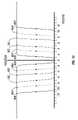
- FIG. 1is an isometric view depicting two adjacent pixels in a series of pixels of a visual display, wherein each pixel comprises a MEMS interferometric modulator.
- an interferometric modulator displaycomprises a row/column array of these interferometric modulators.
- Each interferometric modulatorincludes a pair of reflective layers positioned at a variable and controllable distance from each other to form a resonant optical cavity with at least one variable dimension.
- one of the reflective layersmay be moved between two positions. In the first position, referred to herein as the relaxed position, the movable reflective layer is positioned at a relatively large distance from a fixed partially reflective layer.
- the movable reflective layerIn the second position, referred to herein as the actuated position, the movable reflective layer is positioned more closely adjacent to the partially reflective layer. Incident light that reflects from the two layers interferes constructively or destructively depending on the position of the movable reflective layer, producing either an overall reflective or non-reflective state for each pixel.
- the depicted portion of the pixel array in FIG. 1includes two adjacent interferometric modulators 12 a and 12 b .
- a movable reflective layer 14 aIn the interferometric modulator 12 a on the left, a movable reflective layer 14 a is illustrated in a relaxed position at a predetermined distance from an optical stack 16 a , which includes a partially reflective layer.
- the movable reflective layer 14 bIn the interferometric modulator 12 b on the right, the movable reflective layer 14 b is illustrated in an actuated position adjacent to the optical stack 16 b.
- optical stack 16typically comprise several fused layers, which can include an electrode layer, such as indium tin oxide (ITO), a partially reflective layer, such as chromium, and a transparent dielectric.
- ITOindium tin oxide
- the optical stack 16is thus electrically conductive, partially transparent, and partially reflective, and may be fabricated, for example, by depositing one or more of the above layers onto a transparent substrate 20 .
- the partially reflective layercan be formed from a variety of materials that are partially reflective such as various metals, semiconductors, and dielectrics.
- the partially reflective layercan be formed of one or more layers of materials, and each of the layers can be formed of a single material or a combination of materials.
- the layers of the optical stack 16are patterned into parallel strips, and may form row electrodes in a display device as described further below.
- the movable reflective layers 14 a , 14 bmay be formed as a series of parallel strips of a deposited metal layer or layers (orthogonal to the row electrodes of 16 a , 16 b ) deposited on top of posts 18 and an intervening sacrificial material deposited between the posts 18 . When the sacrificial material is etched away, the movable reflective layers 14 a , 14 b are separated from the optical stacks 16 a , 16 b by a defined gap 19 .
- a highly conductive and reflective materialsuch as aluminum may be used for the reflective layers 14 , and these strips may form column electrodes in a display device.
- the cavity 19remains between the movable reflective layer 14 a and optical stack 16 a , with the movable reflective layer 14 a in a mechanically relaxed state, as illustrated by the pixel 12 a in FIG. 1 .
- a potential differenceis applied to a selected row and column, the capacitor formed at the intersection of the row and column electrodes at the corresponding pixel becomes charged, and electrostatic forces pull the electrodes together.
- the movable reflective layer 14is deformed and is forced against the optical stack 16 .
- a dielectric layerwithin the optical stack 16 may prevent shorting and control the separation distance between layers 14 and 16 , as illustrated by pixel 12 b on the right in FIG. 1 .
- the behavioris the same regardless of the polarity of the applied potential difference. In this way, row/column actuation that can control the reflective vs. non-reflective pixel states is analogous in many ways to that used in conventional LCD and other display technologies.
- FIGS. 2 through 5Billustrate one exemplary process and system for using an array of interferometric modulators in a display application.
- FIG. 2is a system block diagram illustrating one embodiment of an electronic device that may incorporate aspects of the invention.
- the electronic deviceincludes a processor 21 which may be any general purpose single- or multi-chip microprocessor such as an ARM, Pentium®, Pentium II®, Pentium III®, Pentium IV®, Pentium® Pro, an 8051, a MIPS®, a Power PC®, an ALPHA®, or any special purpose microprocessor such as a digital signal processor, microcontroller, or a programmable gate array.
- the processor 21may be configured to execute one or more software modules.
- the processormay be configured to execute one or more software applications, including a web browser, a telephone application, an email program, or any other software application.
- the processor 21is also configured to communicate with an array driver 22 .
- the array driver 22includes a row driver circuit 24 and a column driver circuit 26 that provide signals to a display array or panel 30 .
- the cross section of the array illustrated in FIG. 1is shown by the lines 1 - 1 in FIG. 2 .
- the row/column actuation protocolmay take advantage of a hysteresis property of these devices illustrated in FIG. 3 . It may require, for example, a 10 volt potential difference to cause a movable layer to deform from the relaxed state to the actuated state. However, when the voltage is reduced from that value, the movable layer maintains its state as the voltage drops back below 10 volts.
- the movable layerdoes not relax completely until the voltage drops below 2 volts.
- a window of applied voltageabout 3 to 7 V in the example illustrated in FIG. 3 , within which the device is stable in either the relaxed or actuated state. This is referred to herein as the “hysteresis window” or “stability window.”
- the row/column actuation protocolcan be designed such that during row strobing, pixels in the strobed row that are to be actuated are exposed to a voltage difference of about 10 volts, and pixels that are to be relaxed are exposed to a voltage difference of close to zero volts.
- each pixelsees a potential difference within the “stability window” of 3-7 volts in this example.
- This featuremakes the pixel design illustrated in FIG. 1 stable under the same applied voltage conditions in either an actuated or relaxed pre-existing state. Since each pixel of the interferometric modulator, whether in the actuated or relaxed state, is essentially a capacitor formed by the fixed and moving reflective layers, this stable state can be held at a voltage within the hysteresis window with almost no power dissipation. Essentially no current flows into the pixel if the applied potential is fixed.
- a display framemay be created by asserting the set of column electrodes in accordance with the desired set of actuated pixels in the first row.
- a row pulseis then applied to the row 1 electrode, actuating the pixels corresponding to the asserted column lines.
- the asserted set of column electrodesis then changed to correspond to the desired set of actuated pixels in the second row.
- a pulseis then applied to the row 2 electrode, actuating the appropriate pixels in row 2 in accordance with the asserted column electrodes.
- the row 1 pixelsare unaffected by the row 2 pulse, and remain in the state they were set to during the row 1 pulse. This may be repeated for the entire series of rows in a sequential fashion to produce the frame.
- the framesare refreshed and/or updated with new display data by continually repeating this process at some desired number of frames per second.
- protocols for driving row and column electrodes of pixel arrays to produce display framesare also well known and may be used in conjunction with the present invention.
- FIGS. 4 , 5 A, and 5 Billustrate one possible actuation protocol for creating a display frame on the 3 ⁇ 3 array of FIG. 2 .
- FIG. 4illustrates a possible set of column and row voltage levels that may be used for pixels exhibiting the hysteresis curves of FIG. 3 .
- actuating a pixelinvolves setting the appropriate column to ⁇ V bias , and the appropriate row to + ⁇ V, which may correspond to ⁇ 5 volts and +5 volts, respectively Relaxing the pixel is accomplished by setting the appropriate column to +V bias , and the appropriate row to the same + ⁇ V, producing a zero volt potential difference across the pixel.
- the pixelsare stable in whatever state they were originally in, regardless of whether the column is at +V bias , or ⁇ V bias .
- voltages of opposite polarity than those described abovecan be used, e.g., actuating a pixel can involve setting the appropriate column to +V bias , and the appropriate row to ⁇ V.
- releasing the pixelis accomplished by setting the appropriate column to ⁇ V bias , and the appropriate row to the same ⁇ V, producing a zero volt potential difference across the pixel.
- FIG. 5Bis a timing diagram showing a series of row and column signals applied to the 3 ⁇ 3 array of FIG. 2 which will result in the display arrangement illustrated in FIG. 5A , where actuated pixels are non-reflective.
- the pixelsPrior to writing the frame illustrated in FIG. 5A , the pixels can be in any state, and in this example, all the rows are at 0 volts, and all the columns are at +5 volts. With these applied voltages, all pixels are stable in their existing actuated or relaxed states.
- pixels ( 1 , 1 ), ( 1 , 2 ), ( 2 , 2 ), ( 3 , 2 ) and ( 3 , 3 )are actuated.
- columns 1 and 2are set to ⁇ 5 volts
- column 3is set to +5 volts. This does not change the state of any pixels, because all the pixels remain in the 3-7 volt stability window.
- Row 1is then strobed with a pulse that goes from 0, up to 5 volts, and back to zero. This actuates the ( 1 , 1 ) and ( 1 , 2 ) pixels and relaxes the ( 1 , 3 ) pixel. No other pixels in the array are affected.
- row 2is set to ⁇ 5 volts, and columns 1 and 3 are set to +5 volts.
- the same strobe applied to row 2will then actuate pixel ( 2 , 2 ) and relax pixels ( 2 , 1 ) and ( 2 , 3 ). Again, no other pixels of the array are affected.
- Row 3is similarly set by setting columns 2 and 3 to ⁇ 5 volts, and column 1 to +5 volts.
- the row 3strobe sets the row 3 pixels as shown in FIG. 5A . After writing the frame, the row potentials are zero, and the column potentials can remain at either +5 or ⁇ 5 volts, and the display is then stable in the arrangement of FIG. 5A .
- FIGS. 6A and 6Bare system block diagrams illustrating an embodiment of a display device 40 .
- the display device 40can be, for example, a cellular or mobile telephone.
- the same components of display device 40 or slight variations thereofare also illustrative of various types of display devices such as televisions and portable media players.
- the display device 40includes a housing 41 , a display 30 , an antenna 43 , a speaker 44 , an input device 48 , and a microphone 46 .
- the housing 41is generally formed from any of a variety of manufacturing processes as are well known to those of skill in the art, including injection molding and vacuum forming.
- the housing 41may be made from any of a variety of materials, including, but not limited to, plastic, metal, glass, rubber, and ceramic, or a combination thereof.
- the housing 41includes removable portions (not shown) that may be interchanged with other removable portions of different color, or containing different logos, pictures, or symbols.
- the display 30 of exemplary display device 40may be any of a variety of displays, including a bi-stable display, as described herein.
- the display 30includes a flat-panel display, such as plasma, EL, OLED, STN LCD, or TFT LCD as described above, or a non-flat-panel display, such as a CRT or other tube device, as is well known to those of skill in the art.
- the display 30includes an interferometric modulator display, as described herein.
- the components of one embodiment of exemplary display device 40are schematically illustrated in FIG. 6B .
- the illustrated exemplary display device 40includes a housing 41 and can include additional components at least partially enclosed therein.
- the exemplary display device 40includes a network interface 27 that includes an antenna 43 , which is coupled to a transceiver 47 .
- the transceiver 47is connected to a processor 21 , which is connected to conditioning hardware 52 .
- the conditioning hardware 52may be configured to condition a signal (e.g., filter a signal).
- the conditioning hardware 52is connected to a speaker 45 and a microphone 46 .
- the processor 21is also connected to an input device 48 and a driver controller 29 .
- the driver controller 29is coupled to a frame buffer 28 and to an array driver 22 , which in turn is coupled to a display array 30 .
- a power supply 50provides power to all components as required by the particular exemplary display device 40 design.
- the network interface 27includes the antenna 43 and the transceiver 47 so that the exemplary display device 40 can communicate with one or more devices over a network. In one embodiment, the network interface 27 may also have some processing capabilities to relieve requirements of the processor 21 .
- the antenna 43is any antenna known to those of skill in the art for transmitting and receiving signals. In one embodiment, the antenna transmits and receives RF signals according to the IEEE 802.11 standard, including IEEE 802.11(a), (b), or (g). In another embodiment, the antenna transmits and receives RF signals according to the BLUETOOTH standard. In the case of a cellular telephone, the antenna is designed to receive CDMA, GSM, AMPS, or other known signals that are used to communicate within a wireless cell phone network.
- the transceiver 47pre-processes the signals received from the antenna 43 so that they may be received by and further manipulated by the processor 21 .
- the transceiver 47also processes signals received from the processor 21 so that they may be transmitted from the exemplary display device 40 via the antenna 43 .
- the transceiver 47can be replaced by a receiver.
- network interface 27can be replaced by an image source, which can store or generate image data to be sent to the processor 21 .
- the image sourcecan be a digital video disc (DVD) or a hard-disk drive that contains image data, or a software module that generates image data.
- Processor 21generally controls the overall operation of the exemplary display device 40 .
- the processor 21receives data, such as compressed image data from the network interface 27 or an image source, and processes the data into raw image data or into a format that is readily processed into raw image data.
- the processor 21then sends the processed data to the driver controller 29 or to frame buffer 28 for storage.
- Raw datatypically refers to the information that identifies the image characteristics at each location within an image. For example, such image characteristics can include color, saturation, and gray-scale level.
- the processor 21includes a microcontroller, CPU, or logic unit to control operation of the exemplary display device 40 .
- Conditioning hardware 52generally includes amplifiers and filters for transmitting signals to the speaker 45 , and for receiving signals from the microphone 46 .
- Conditioning hardware 52may be discrete components within the exemplary display device 40 , or may be incorporated within the processor 21 or other components.
- the driver controller 29takes the raw image data generated by the processor 21 either directly from the processor 21 or from the frame buffer 28 and reformats the raw image data appropriately for high speed transmission to the array driver 22 . Specifically, the driver controller 29 reformats the raw image data into a data flow having a raster-like format, such that it has a time order suitable for scanning across the display array 30 . Then the driver controller 29 sends the formatted information to the array driver 22 .
- a driver controller 29such as a LCD controller, is often associated with the system processor 21 as a stand-alone Integrated Circuit (IC), such controllers may be implemented in many ways. They may be embedded in the processor 21 as hardware, embedded in the processor 21 as software, or fully integrated in hardware with the array driver 22 .
- the array driver 22receives the formatted information from the driver controller 29 and reformats the video data into a parallel set of waveforms that are applied many times per second to the hundreds and sometimes thousands of leads coming from the display's x-y matrix of pixels.
- driver controller 29is a conventional display controller or a bi-stable display controller (e.g., an interferometric modulator controller).
- array driver 22is a conventional driver or a bi-stable display driver (e.g., an interferometric modulator display).
- a driver controller 29is integrated with the array driver 22 .
- display array 30is a typical display array or a bi-stable display array (e.g., a display including an array of interferometric modulators).
- the input device 48allows a user to control the operation of the exemplary display device 40 .
- input device 48includes a keypad, such as a QWERTY keyboard or a telephone keypad, a button, a switch, a touch-sensitive screen, or a pressure- or heat-sensitive membrane.
- the microphone 46is an input device for the exemplary display device 40 . When the microphone 46 is used to input data to the device, voice commands may be provided by a user for controlling operations of the exemplary display device 40 .
- Power supply 50can include a variety of energy storage devices as are well known in the art.
- power supply 50is a rechargeable battery, such as a nickel-cadmium battery or a lithium ion battery.
- power supply 50is a renewable energy source, a capacitor, or a solar cell, including a plastic solar cell and solar-cell paint.
- power supply 50is configured to receive power from a wall outlet.
- control programmabilityresides, as described above, in a driver controller which can be located in several places in the electronic display system. In some embodiments, control programmability resides in the array driver 22 . Those of skill in the art will recognize that the above-described optimizations may be implemented in any number of hardware and/or software components and in various configurations.
- FIGS. 7A-7Eillustrate five different embodiments of the movable reflective layer 14 and its supporting structures.
- FIG. 7Ais a cross section of the embodiment of FIG. 1 , where a strip of metal material 14 is deposited on orthogonally extending supports 18 .
- FIG. 7Bthe moveable reflective layer 14 is attached to supports at the corners only, on tethers 32 .
- FIG. 7Cthe moveable reflective layer 14 is suspended from a deformable layer 34 , which may comprise a flexible metal.
- the deformable layer 34connects, directly or indirectly, to the substrate 20 around the perimeter of the deformable layer 34 .
- connection postsare herein referred to as support posts.
- the embodiment illustrated in FIG. 7Dhas support post plugs 42 upon which the deformable layer 34 rests.
- the movable reflective layer 14remains suspended over the cavity, as in FIGS. 7A-7C , but the deformable layer 34 does not form the support posts by filling holes between the deformable layer 34 and the optical stack 16 . Rather, the support posts are formed of a planarization material, which is used to form support post plugs 42 .
- the embodiment illustrated in FIG. 7Eis based on the embodiment shown in FIG. 7D , but may also be adapted to work with any of the embodiments illustrated in FIGS. 7A-7C , as well as additional embodiments not shown. In the embodiment shown in FIG. 7E , an extra layer of metal or other conductive material has been used to form a bus structure 44 . This allows signal routing along the back of the interferometric modulators, eliminating a number of electrodes that may otherwise have had to be formed on the substrate 20 .
- the interferometric modulatorsfunction as direct-view devices, in which images are viewed from the front side of the transparent substrate 20 , the side opposite to that upon which the modulator is arranged.
- the reflective layer 14optically shields the portions of the interferometric modulator on the side of the reflective layer opposite the substrate 20 , including the deformable layer 34 . This allows the shielded areas to be configured and operated upon without negatively affecting the image quality.
- Such shieldingallows the bus structure 44 in FIG. 7E , which provides the ability to separate the optical properties of the modulator from the electromechanical properties of the modulator, such as addressing and the movements that result from that addressing.
- This separable modulator architectureallows the structural design and materials used for the electromechanical aspects and the optical aspects of the modulator to be selected and to function independently of each other.
- the embodiments shown in FIGS. 7C-7Ehave additional benefits deriving from the decoupling of the optical properties of the reflective layer 14 from its mechanical properties, which are carried out by the deformable layer 34 .
- Thisallows the structural design and materials used for the reflective layer 14 to be optimized with respect to the optical properties, and the structural design and materials used for the deformable layer 34 to be optimized with respect to desired mechanical properties.
- FIG. 8illustrates one embodiment of a monochrome display including one interferometric modulator per pixel, the “on” or “off” state of the modulator being set based on the value of the one bit of data per pixel.
- the pixelis configured to communicate with one column conduit and one row conduit.
- a grayscale imagemay include several bits of data per pixel.
- a “3-bit” grayscale displayincludes three bits of data per pixel that correspond to one of eight (2 3 ) shades of gray that may be assigned to each pixel.
- the pixelis configured to communicate with one column conduit and three row conduits.
- each of the interferometric modulators 91 , 92 , 93includes mirrors having a reflective surface area that varies according to the ratio of 4:2:1.
- the reflective portion of one mirror or modulatormay be referred to as “subtending” a portion of the pixel.
- the mirror with a surface area of one in the 4:2:1 embodimentsubtends about 1/7 of the pixel.
- a particular shade in a pixelis obtained by setting each modulator to an “on” or “off” state based on the binary value of a corresponding bit of the three bits of data.
- FIG. 10illustrates one embodiment of a color display having pixel 100 that works similarly to the grayscale pixel 90 of FIG. 9 , except that the pixel 100 includes a group of red interferometric modulators 101 , 102 , 103 , green interferometric modulators 104 , 105 , 106 , and blue interferometric modulators 107 , 108 , 109 .
- the pixel 100is responsive to a 9-bit signal in which three groups of 3 bits each correspond to the three colors.
- four of the twelve bitscorrespond to each of sixteen intensities of red, green, and blue that are produced by red, green, or blue interferometric modulators.
- FIG. 11illustrates one embodiment of a 3-bit grayscale display in which the pixels are in a 3 ⁇ 3 configuration with each of the three rows subdivided into three subrows of modulators.
- Such an embodimenthas nine row driver connections and three column driver connections for a total of twelve driver connections rather than the six driver connections used for a 3 ⁇ 3 monochrome display.
- One way of reducing the number of driver connectionsis to configure a group of modulators to communicate with a single row conduit, for example (as depicted in FIG. 12 ), the three subrows in the 3-bit grayscale embodiment discussed above, and drive the group with a signal that changes the state of a selected subset of the group.
- the interferometric modulators of each of the subrowsmay have varying actuation and release voltages so as to enable a group of subrows that are configured to communicate with a single row conduit to be individually addressed.
- FIG. 13is a diagram of movable mirror position versus applied positive and negative voltage illustrating one exemplary embodiment of three interferometric modulators that have nested stability windows.
- the term “nested”is to mean with exploitable differences in both actuation voltages and release voltages.
- the innermost nested hysteresis window, indicated by the traces 802has actuation and release voltages having magnitudes of 8 volts and 4 volts, respectively.
- This hysteresis windowis nested in the hysteresis window indicated by traces 804 and is nested in the hysteresis window indicated by traces 806 .
- the next nested hysteresis window, indicated by the traces 804has actuation and release voltages having magnitudes of 10 volts and 2 volts, respectively.
- This hysteresis windowis nested in the hysteresis window indicated by traces 806 .
- the outermost hysteresis window, indicated by the traces 806has actuation and release voltages having magnitudes of 12 volts and 0 volts, respectively.
- the hysteresis window of the modulators associated with each subrowmay be selected by varying the geometry and/or materials of the modulators.
- the width (difference between the actuation and release voltages), the location (the absolute values of the actuation and release voltages), and the relative values of the actuation and release voltagesmay be selected by varying geometric and material properties of the modulators.
- the varied propertiesmay include, for example, the distance between movable mirror supports, the mass associated with the movable mirror relative to the spring constant, the thickness, tensile stress, or stiffness of the mirror and/or the layers or mechanism that moves the mirror, and the dielectric constant and/or thickness of a dielectric layer between the stationary electrode and the movable electrode.
- the interferometric modulatorsare arranged as in FIG. 12 .
- the stability windowsare nested from outer to inner, such as the windows depicted in FIG. 13 , from the top subrow to the bottom subrow.
- FIG. 14is an exemplary timing diagram that illustrates a series of row and column signals applied to the top row (Row 1 ) of such an embodiment to produce the display arrangement illustrated in Row 1 of FIG. 12 .
- the positive voltage regime and the negative voltage regimeare substantially equivalent to one another, as shown in FIG. 13 .
- the interferometric modulatorscan be similarly operated in the negative voltage regime.
- the row pulsesdecrease in magnitude from left to right, corresponding to the subrows from top to bottom. This decreasing magnitude of the pulses is selected to address only those modulators in subrows that have smaller actuation and greater release voltages. For example, in the illustrated embodiment, potentials of +6 and ⁇ 6 volts are applied to the columns and row pulses of +6, +4, and +2 volts are applied to the rows.
- the pulses of FIG. 14set the state of Row 1 of the display to that depicted in FIG. 12 as follows. For the first line time for Row 1 , Column 1 , a Column 1 potential of ⁇ 6 volts is applied along with a row pulse of +6 volts, producing a 12-volt difference across the modulators of Row 1 , Column 1 , to set the state of the modulators of each of the Row 1 , Column 1 subrows in the actuated position as illustrated along the bottom of FIG. 14 . The Column 1 potential remains at ⁇ 6 for the remaining Row 1 line times to continue to set the state of each of the elements in the Row 1 , Column 1 subrows to the actuated position.
- a Column 2 potential of +6 voltsis applied in conjunction with the row pulse at +6 volts in the first line time, producing a zero-volt difference across the modulators of Row 1 , Column 2 , to release all modulators in the subrows in Row 1 , Column 2 .
- a Column 2 potential of ⁇ 6 voltsis applied in conjunction with a row pulse of +4 volts, producing a 10-volt difference across the modulators of Row 1 , Column 2 , to actuate the bottom two subrows of Row 1 , Column 2 .
- a Column 2 potentialis applied at +6 volts in conjunction with a row pulse of +2 volts, producing a 4-volt difference across the modulators of Row 1 , Column 2 , to release the modulator in the bottom subrow of Row 1 , Column 2 .
- a Column 3 potential of ⁇ 6 voltsis applied in conjunction with the row pulse at +6 volts in the first line time, producing a 12-volt difference across the modulators of Row 1 , Column 3 , to actuate all modulators in the subrows in Row 1 , Column 3 .
- a Column 3 potential of +6 voltsis applied in conjunction with a row pulse of +4 volts, producing a 2-volt difference across the modulators of Row 1 , Column 3 , to release the bottom two subrows of Row 1 , Column 3 .
- a Column 3 potentialis applied at ⁇ 6 volts in conjunction with the row pulse of +2 volts, producing an 8-volt difference across the modulators of Row 1 , Column 3 , to actuate the modulator in the bottom subrow of Row 1 , Column 3 .
- FIG. 15is a flowchart illustrating one embodiment of a method 850 of updating an embodiment of a display such as depicted in FIG. 12 .
- the method 850begins at a block 852 in which the driver 22 of FIG. 2 receives image data value for a subrow. In one embodiment, the driver 22 receives the data value from a frame buffer.
- the driver 22applies a row strobe to all subrows of interferometric modulators along with a column potential that corresponds to the image data value.
- the driver 22receives the data for the next subrow.
- the acts of blocks 854 and 856are repeated for each of the subrows. In one embodiment, the acts of the blocks 854 and 856 occur at least partially concurrently.
- At least one aspect of the present inventionis the realization that quantization artifacts are more visible to the user in low-intensity regions than in high-intensity regions because the percentage change between quantization levels is greater at lower intensities.
- quantization artifactsare more visible to the user in low-intensity regions than in high-intensity regions because the percentage change between quantization levels is greater at lower intensities.
- the intensity change from level 100 to level 101is 1%. Most users cannot discern intensity changes below about 4%, so transitions at or below this quantization level appear smooth. However, the change from level 10 to level 11 is 10%, an intensity change that is easily seen by most users. Therefore, at low intensity quantization levels, the quantization of analog data into discrete digitized quantization steps is clearly seen as an artifact. The most straightforward approach to this problem is to digitize at higher bit densities.
- the transition from level 80 to level 81is about 1.2%, and would then be indiscernible to the user.
- such increases in system bit densitycan lead to greater system complexity and cost (e.g., the number of driver connections would increase by about 38% from 24 in a 3 ⁇ 3 7-bit grayscale display to 33 in a 3 ⁇ 3 10-bit grayscale display).
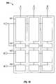
- FIG. 16is a schematic diagram of an embodiment of a color interferometric modulator pixel 160 .
- the interferometric modulator 101 of FIG. 10has been partitioned or replaced by two interferometric modulators 161 , 162 (or “display elements”) arranged in two subrows that are configured to communicate with a common row conduit.
- the modulator 101subtends about 4/7 of the area of the first column.
- the modulator 161subtends about half ( 7/14) of the first column and the modulator 162 subtends about 1/14 of the first column.
- the first display element 161has a first optically active area and the second display element 162 has a second optically active area.
- the ratio of the first optically active area to the second optically active areais approximately equal to an integer to one (e.g., 7 to 1, 7:1, 7/1).
- the integeris 2, 3, 4, 5, 6, 7, 8, 9, or 10.
- the integeris 3, 7, 15, 31, 63, 127, 255, or any number 2 n -1 where n is an integer greater than or equal to 2.
- FIG. 16represents an embodiment partitioning the modulators 101 , 104 , and 107 in FIG. 10 , such partitioning may also be appropriate for grayscale displays (e.g., by partitioning the modulator 91 depicted in FIG. 9 ).
- the terms “divided,” “partitioned,” and “replaced” in relation to the plurality of interferometric modulators or mirrors of various embodimentsdoes not require that a larger interferometric modulator or mirror actually be created and then partitioned into smaller interferometric modulators or mirrors. Instead, the terms are used to compare the relative structures from previously described configurations.
- the modulators 161 and 162 in FIG. 16are typically formed independently from one another, as opposed to having been formed as a single modulator 101 as depicted in FIG. 10 and then partitioned into smaller modulators.
- independent creationis preferable in some embodiments to allow for individual adjustment of the hysteresis curves for the modulators 161 , 162 as described above.
- FIG. 17is a diagram of modulator position versus applied positive voltage illustrating one exemplary embodiment of two interferometric modulators (e.g., the two modulators 161 , 162 illustrated in FIG. 16 ) that have hysteresis curve stability windows in which the actuation voltages are different, but the release voltages are about the same.
- the traces 810represent the hysteresis loop of the modulator 161 and the traces 808 represent the hysteresis loop of the modulator 162 .
- the release voltages of the two modulators 161 , 162are considered to be substantially equal to one another when any differences between the respective release voltages are not used to selectively release one of the modulators and not the other.
- the hysteresis loop depicted by the traces 808has an actuation voltage of about 9 volts and a release voltage of about 1 volt.
- the hysteresis loop represented by the traces 810has an actuation voltage of about 15 volts and has a release voltage of about 1 volt. Because the release voltages of the hysteresis loops of FIG. 17 are not exploitably different from each other (i.e., there are no voltages that can be applied to reliably release one modulator and not the other modulator), the hysteresis loops of FIG. 17 cannot be said to be “nested” as defined herein.
- FIG. 18is a diagram of modulator position versus applied positive voltage illustrating another exemplary embodiment of two interferometric modulators (e.g., the two modulators 161 , 162 illustrated in FIG. 16 ) that have different stability windows in which the release voltages are different, but the actuation voltages are about the same.
- the traces 814represent the hysteresis loop of the modulator 161 and the traces 812 represent the hysteresis loop of the modulator 162 .
- the actuation voltages of the two modulators 161 , 162are considered to be substantially equal to one another when any differences between the respective actuation voltages are not used to selectively actuate one of the modulators and not the other modulator.
- the hysteresis loop depicted by the traces 812has an actuation voltage of about 15 volts and a release voltage of about 6 volts.
- the hysteresis loop represented by the traces 814has an actuation voltage of about 15 volts, but has a release voltage of about 1 volt. Because the actuation voltages of the hysteresis loops of FIG. 18 are not exploitably different from each other (i.e., there are no voltages that can be applied to reliably actuate one modulator and not the other modulator), these hysteresis loops cannot be said to be “nested” as defined herein.
- each of the nested hysteresis loops of FIG. 13are proximate to each other.
- the release voltage for the loop 804is about 2 volts and the release voltage for the loop 802 is about 4 volts.
- the voltage appliedwould be between 2 and 4 volts, preferably around 3 volts.
- This voltage accuracycan present problems if the manufacturing tolerances of the modulators that release at 2 volts and 4 volts are not sufficiently precise. For example, if the modulator represented by loop 802 was manufactured such that its release voltage was 3.5 volts and the modulator represented by loop 804 was manufactured such that its release voltage was 2.5 volts, the tolerance window for the applied voltage would shrink considerably.
- the applied voltagemay also vary with manufacturing tolerances such that an application of 3 volts to the modulator may actually result in a voltage difference across the modulator closer to 2.5 volts.
- a voltage applied to the modulators to release the modulator represented by loop 802may inadvertently also release the modulator represented by loop 804 .
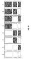
- FIG. 19schematically illustrates the quantization levels provided by the schematic of FIG. 10 . None of the modulators are in the “on” state in level 0 and all of the modulators are in the “on” state in level 7 . Some of the modulators are in the “on” state in levels 1 through 6 , providing varying amounts of intensity.
- the bit density at low intensity rangesis the same as the bit density at high intensity ranges.
- the intensity difference between sequential quantization steps for intensities below level 4e.g., intensity difference of one
- the intensity difference between sequential quantization steps for intensities above level 4e.g., intensity difference of one).
- the two modulators 161 , 162 of FIG. 16 having the hysteresis curves 810 , 808 of FIG. 17are used in certain embodiments to provide a higher bit density at lower intensity ranges than at higher intensity ranges.
- the modulator 161is actuated or placed in an “on” state only for levels 4 and above.
- the actuation drive voltage on the modulators 161 , 162can be reduced so that only the modulator 162 is selectively actuated.
- this modulator 162has a mirror with preferably about one-half the optical weight of the mirror of the modulator 164 , the modulators 162 , 164 , and 163 have weights in the ratio 1:2:4, respectively, and can be used to generate eight quantization steps below quantization level 4 , as illustrated in FIG. 21 .
- the quantization steps below level 4are illustrated in FIG. 22 .
- the two modulators 161 , 162 of FIG. 16 having the hysteresis curves 814 , 812 of FIG. 18are used in certain other embodiments to provide a higher bit density at lower intensity ranges than at higher intensity ranges.
- the number of sequential quantization stepsare more than doubled in the lower portion of the display intensity range, which is the portion of the quantization range most in need of finer quantization.
- the number of sequential quantization steps for intensities below level 4 (i.e., eight) in FIG. 22is more than double the number of sequential quantization steps for intensities above level 4 (i.e., three) in either FIG. 20 or FIG. 22 .
- quantization steprefers to the change from one amount of intensity to the next amount of intensity
- quantization levelrefers to the change from one bit depth to the next bit depth. For example, the change in intensity from one modulator to the next in the top row of FIG.
- FIG. 21is a quantization step, but not a quantization level, while the change in intensity from one modulator to the next modulator in the bottom row of FIG. 21 is both a quantization step and a quantization level. It will be appreciated that the effect is much more pronounced at bit depths greater than 3-bit.
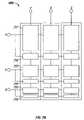
- FIG. 23is a schematic diagram of an embodiment of a color interferometric modulator pixel 230 .
- FIG. 23represents an embodiment partitioning the modulators 102 , 105 , and 108 in FIG. 10 , such partitioning may also be appropriate for grayscale displays (e.g., by partitioning the modulator 92 depicted in FIG. 9 ).
- the modulator 104has been divided into two modulators 232 , 233 (or “display elements”) arranged in subrows that are configured to communicate with a common row conduit.
- the modulator 102subtends about 2/7 of the area of the first column.
- the modulator 232subtends about 3 / 14 of the first column and the modulator 233 subtends about 1/14 of the first column.
- the function of the pixel 200is unchanged from the pixel 100 schematically depicted in FIG. 10 .
- the hysteresis loops for the modulators 232 , 233may share a common actuation voltage or a common release voltage as displayed in FIGS. 17 and 18 .
- the modulators 234 , 233 , 232 , 231subtend the pixel in a ratio of 2:1:3:8, respectively, the number of sequential quantization steps (i.e., two) are doubled below level 2 of the display quantization range, which is part of. the portion of the quantization range most in need of finer quantization.
- the number of sequential quantization stepsi.e., two
- four modulatorsare actuated and released to provide eleven quantization steps, six of which are below the fourth quantization level, as depicted in FIGS. 24 and 25 . Because the schematic illustrated in FIG. 16 provides finer quantization steps between level 2 and level 4 , partitioning the mirror 101 of FIG. 10 is preferred to partitioning the mirror 104 of FIG. 10 .
- Still finer quantizationmay be achieved by partitioning all three mirrors 101 , 104 , and 107 in FIG. 10 , as illustrated by the schematic diagram in FIG. 29 .
- FIG. 30such a configuration results in 26 quantization steps, 18 of which are below the fourth quantization level.
- the number of quantization stepsadvantageously increases from 7 to 26, most of which are in the region of low intensity most in need of finer quantization. This configuration dramatically reduces quantization level spacing at low intensities, the display range where it is most needed, without increasing the number of address lines from the driver IC.
Landscapes
- Engineering & Computer Science (AREA)
- Physics & Mathematics (AREA)
- Computer Hardware Design (AREA)
- General Physics & Mathematics (AREA)
- Theoretical Computer Science (AREA)
- Nonlinear Science (AREA)
- Optics & Photonics (AREA)
- Microelectronics & Electronic Packaging (AREA)
- Mechanical Light Control Or Optical Switches (AREA)
- Control Of Indicators Other Than Cathode Ray Tubes (AREA)
- Micromachines (AREA)
- Devices For Indicating Variable Information By Combining Individual Elements (AREA)
Abstract
Description
Claims (23)
Priority Applications (19)
| Application Number | Priority Date | Filing Date | Title |
|---|---|---|---|
| US11/454,162US7471442B2 (en) | 2006-06-15 | 2006-06-15 | Method and apparatus for low range bit depth enhancements for MEMS display architectures |
| CN2007800219106ACN101467198B (en) | 2006-06-15 | 2007-04-30 | Method and apparatus for low-range bit-depth enhancement for microelectromechanical system display architectures |
| CN201310005807XACN103021350A (en) | 2006-06-15 | 2007-04-30 | Method and apparatus for low range bit depth enhancement for MEMS display architectures |
| KR1020127011236AKR101296143B1 (en) | 2006-06-15 | 2007-04-30 | Apparatus for low range bit depth enhancement for mems display architectures |
| BRPI0712548-8ABRPI0712548A2 (en) | 2006-06-15 | 2007-04-30 | screen, modular light devices and methods of fabrication and light modulation and image display |
| BRPI0722427-3ABRPI0722427A2 (en) | 2006-06-15 | 2007-04-30 | LIGHT MODULATOR DEVICE |
| JP2009515389AJP4981131B2 (en) | 2006-06-15 | 2007-04-30 | Method and apparatus for low range bit depth extension for MEMS display architectures |
| RU2008146783/07ARU2440623C2 (en) | 2006-06-15 | 2007-04-30 | Method and apparatus for increasing low range of colour depth in micromechanical system based displays |
| EP07776536AEP2027575A2 (en) | 2006-06-15 | 2007-04-30 | Method and apparatus for low range bit depth enhancement for mems display architectures |
| EP11175643AEP2383726A1 (en) | 2006-06-15 | 2007-04-30 | Method and apparatus for low range bit depth enhancement for MEMS display architectures |
| PCT/US2007/010499WO2007145720A2 (en) | 2006-06-15 | 2007-04-30 | Method and apparatus for low range bit depth enhancement for mems display architectures |
| KR1020097000664AKR20090023687A (en) | 2006-06-15 | 2007-04-30 | Method and apparatus for low range bit depth enhancement of MEMS display structures |
| CA002654185ACA2654185A1 (en) | 2006-06-15 | 2007-04-30 | Method and apparatus for low range bit depth enhancement for mems display architectures |
| TW096116636ATW200807060A (en) | 2006-06-15 | 2007-05-10 | Method and apparatus for low range bit depth enhancement for MEMS display architectures |
| TW100127608ATW201145246A (en) | 2006-06-15 | 2007-05-10 | Method and apparatus for low range bit depth enhancement for MEMS display architectures |
| US12/345,551US7808695B2 (en) | 2006-06-15 | 2008-12-29 | Method and apparatus for low range bit depth enhancement for MEMS display architectures |
| US12/874,435US7898725B2 (en) | 2006-06-15 | 2010-09-02 | Apparatuses with enhanced low range bit depth |
| JP2011136191AJP2011237812A (en) | 2006-06-15 | 2011-06-20 | Method and apparatus for low range bit depth enhancement for mems display architectures |
| RU2011131707/07ARU2011131707A (en) | 2006-06-15 | 2011-07-28 | METHOD AND DEVICE FOR INCREASING A LOW RANGE OF COLOR DEPTH IN DISPLAYS BASED ON MICROELECTROMECHANICAL SYSTEMS |
Applications Claiming Priority (1)
| Application Number | Priority Date | Filing Date | Title |
|---|---|---|---|
| US11/454,162US7471442B2 (en) | 2006-06-15 | 2006-06-15 | Method and apparatus for low range bit depth enhancements for MEMS display architectures |
Related Child Applications (1)
| Application Number | Title | Priority Date | Filing Date |
|---|---|---|---|
| US12/345,551ContinuationUS7808695B2 (en) | 2006-06-15 | 2008-12-29 | Method and apparatus for low range bit depth enhancement for MEMS display architectures |
Publications (2)
| Publication Number | Publication Date |
|---|---|
| US20070290961A1 US20070290961A1 (en) | 2007-12-20 |
| US7471442B2true US7471442B2 (en) | 2008-12-30 |
Family
ID=38814584
Family Applications (3)
| Application Number | Title | Priority Date | Filing Date |
|---|---|---|---|
| US11/454,162Expired - Fee RelatedUS7471442B2 (en) | 2006-06-15 | 2006-06-15 | Method and apparatus for low range bit depth enhancements for MEMS display architectures |
| US12/345,551Expired - Fee RelatedUS7808695B2 (en) | 2006-06-15 | 2008-12-29 | Method and apparatus for low range bit depth enhancement for MEMS display architectures |
| US12/874,435Expired - Fee RelatedUS7898725B2 (en) | 2006-06-15 | 2010-09-02 | Apparatuses with enhanced low range bit depth |
Family Applications After (2)
| Application Number | Title | Priority Date | Filing Date |
|---|---|---|---|
| US12/345,551Expired - Fee RelatedUS7808695B2 (en) | 2006-06-15 | 2008-12-29 | Method and apparatus for low range bit depth enhancement for MEMS display architectures |
| US12/874,435Expired - Fee RelatedUS7898725B2 (en) | 2006-06-15 | 2010-09-02 | Apparatuses with enhanced low range bit depth |
Country Status (10)
| Country | Link |
|---|---|
| US (3) | US7471442B2 (en) |
| EP (2) | EP2383726A1 (en) |
| JP (2) | JP4981131B2 (en) |
| KR (2) | KR20090023687A (en) |
| CN (2) | CN101467198B (en) |
| BR (2) | BRPI0722427A2 (en) |
| CA (1) | CA2654185A1 (en) |
| RU (2) | RU2440623C2 (en) |
| TW (2) | TW201145246A (en) |
| WO (1) | WO2007145720A2 (en) |
Cited By (14)
| Publication number | Priority date | Publication date | Assignee | Title |
|---|---|---|---|---|
| US20100053477A1 (en)* | 2008-08-26 | 2010-03-04 | Sue Hui | Spatial Light Modulator Sub-Pixel Architecture and Method |
| US7719500B2 (en)* | 2004-09-27 | 2010-05-18 | Qualcomm Mems Technologies, Inc. | Reflective display pixels arranged in non-rectangular arrays |
| US7808695B2 (en) | 2006-06-15 | 2010-10-05 | Qualcomm Mems Technologies, Inc. | Method and apparatus for low range bit depth enhancement for MEMS display architectures |
| US20110043504A1 (en)* | 2009-08-18 | 2011-02-24 | Chang Jaehyuk | Display Apparatus and Method of Driving the Same |
| WO2011130718A2 (en) | 2010-04-16 | 2011-10-20 | Flex Lighting Ii, Llc | Front illumination device comprising a film-based lightguide |
| WO2011130715A2 (en) | 2010-04-16 | 2011-10-20 | Flex Lighting Ii, Llc | Illumination device comprising a film-based lightguide |
| US8270056B2 (en) | 2009-03-23 | 2012-09-18 | Qualcomm Mems Technologies, Inc. | Display device with openings between sub-pixels and method of making same |
| US20130003158A1 (en)* | 2011-06-28 | 2013-01-03 | Qualcomm Mems Technologies, Inc. | Apparatus and method for optical decoupling |
| US8659816B2 (en) | 2011-04-25 | 2014-02-25 | Qualcomm Mems Technologies, Inc. | Mechanical layer and methods of making the same |
| US8817357B2 (en) | 2010-04-09 | 2014-08-26 | Qualcomm Mems Technologies, Inc. | Mechanical layer and methods of forming the same |
| US8964280B2 (en) | 2006-06-30 | 2015-02-24 | Qualcomm Mems Technologies, Inc. | Method of manufacturing MEMS devices providing air gap control |
| US8963159B2 (en) | 2011-04-04 | 2015-02-24 | Qualcomm Mems Technologies, Inc. | Pixel via and methods of forming the same |
| US9134527B2 (en) | 2011-04-04 | 2015-09-15 | Qualcomm Mems Technologies, Inc. | Pixel via and methods of forming the same |
| US9554213B2 (en) | 2012-10-01 | 2017-01-24 | The Research Foundation For The State University Of New York | Hinged MEMS diaphragm |
Families Citing this family (19)
| Publication number | Priority date | Publication date | Assignee | Title |
|---|---|---|---|---|
| US8310441B2 (en) | 2004-09-27 | 2012-11-13 | Qualcomm Mems Technologies, Inc. | Method and system for writing data to MEMS display elements |
| US20080111834A1 (en)* | 2006-11-09 | 2008-05-15 | Mignard Marc M | Two primary color display |
| US7916378B2 (en)* | 2007-03-08 | 2011-03-29 | Qualcomm Mems Technologies, Inc. | Method and apparatus for providing a light absorbing mask in an interferometric modulator display |
| US8111262B2 (en) | 2007-05-18 | 2012-02-07 | Qualcomm Mems Technologies, Inc. | Interferometric modulator displays with reduced color sensitivity |
| US7847999B2 (en) | 2007-09-14 | 2010-12-07 | Qualcomm Mems Technologies, Inc. | Interferometric modulator display devices |
| US7944604B2 (en) | 2008-03-07 | 2011-05-17 | Qualcomm Mems Technologies, Inc. | Interferometric modulator in transmission mode |
| US7969638B2 (en) | 2008-04-10 | 2011-06-28 | Qualcomm Mems Technologies, Inc. | Device having thin black mask and method of fabricating the same |
| US7791783B2 (en)* | 2008-06-25 | 2010-09-07 | Qualcomm Mems Technologies, Inc. | Backlight displays |
| KR101542400B1 (en)* | 2008-12-29 | 2015-08-07 | 삼성디스플레이 주식회사 | Display device and driving method thereof |
| US8736590B2 (en)* | 2009-03-27 | 2014-05-27 | Qualcomm Mems Technologies, Inc. | Low voltage driver scheme for interferometric modulators |
| US20110148837A1 (en)* | 2009-12-18 | 2011-06-23 | Qualcomm Mems Technologies, Inc. | Charge control techniques for selectively activating an array of devices |
| US8872804B2 (en)* | 2011-07-21 | 2014-10-28 | Qualcomm Mems Technologies, Inc. | Touch sensing display devices and related methods |
| JP2015501944A (en)* | 2011-11-11 | 2015-01-19 | クォルコム・メムズ・テクノロジーズ・インコーポレーテッド | System, device and method for driving a display |
| US20140168223A1 (en)* | 2012-12-13 | 2014-06-19 | Qualcomm Mems Technologies, Inc. | Pixel actuation voltage tuning |
| ES2880740T3 (en) | 2013-05-07 | 2021-11-25 | Dolby Laboratories Licensing Corp | Multiple halftone imaging and dual modulation projection / dual modulation laser projection |
| US10341622B2 (en) | 2013-05-07 | 2019-07-02 | Dolby Laboratories Licensing Corporation | Multi-half-tone imaging and dual modulation projection/dual modulation laser projection |
| US20150317944A1 (en)* | 2014-05-02 | 2015-11-05 | Qualcomm Incorporated | Mobile device based color management of digital displays |
| US20150317928A1 (en)* | 2014-05-02 | 2015-11-05 | Qualcomm Incorporated | Mobile device based color management of digital displays |
| CN110190093A (en)* | 2019-05-22 | 2019-08-30 | 武汉华星光电半导体显示技术有限公司 | The control method of OLED display panel and its light emission luminance |
Citations (414)
| Publication number | Priority date | Publication date | Assignee | Title |
|---|---|---|---|---|
| US2534846A (en) | 1946-06-20 | 1950-12-19 | Emi Ltd | Color filter |
| US3037189A (en) | 1958-04-23 | 1962-05-29 | Sylvania Electric Prod | Visual display system |
| US3210757A (en) | 1962-01-29 | 1965-10-05 | Carlyle W Jacob | Matrix controlled light valve display apparatus |
| US3439973A (en) | 1963-06-28 | 1969-04-22 | Siemens Ag | Polarizing reflector for electromagnetic wave radiation in the micron wavelength |
| US3653741A (en) | 1970-02-16 | 1972-04-04 | Alvin M Marks | Electro-optical dipolar material |
| US3656836A (en) | 1968-07-05 | 1972-04-18 | Thomson Csf | Light modulator |
| US3725868A (en) | 1970-10-19 | 1973-04-03 | Burroughs Corp | Small reconfigurable processor for a variety of data processing applications |
| US3813265A (en) | 1970-02-16 | 1974-05-28 | A Marks | Electro-optical dipolar material |
| US3955880A (en) | 1973-07-20 | 1976-05-11 | Organisation Europeenne De Recherches Spatiales | Infrared radiation modulator |
| US4099854A (en) | 1976-10-12 | 1978-07-11 | The Unites States Of America As Represented By The Secretary Of The Navy | Optical notch filter utilizing electric dipole resonance absorption |
| US4196396A (en) | 1976-10-15 | 1980-04-01 | Bell Telephone Laboratories, Incorporated | Interferometer apparatus using electro-optic material with feedback |
| US4228437A (en) | 1979-06-26 | 1980-10-14 | The United States Of America As Represented By The Secretary Of The Navy | Wideband polarization-transforming electromagnetic mirror |
| US4377324A (en) | 1980-08-04 | 1983-03-22 | Honeywell Inc. | Graded index Fabry-Perot optical filter device |
| US4389096A (en) | 1977-12-27 | 1983-06-21 | Matsushita Electric Industrial Co., Ltd. | Image display apparatus of liquid crystal valve projection type |
| US4392711A (en) | 1980-03-28 | 1983-07-12 | Hoechst Aktiengesellschaft | Process and apparatus for rendering visible charge images |
| US4403248A (en) | 1980-03-04 | 1983-09-06 | U.S. Philips Corporation | Display device with deformable reflective medium |
| US4441791A (en) | 1980-09-02 | 1984-04-10 | Texas Instruments Incorporated | Deformable mirror light modulator |
| US4445050A (en) | 1981-12-15 | 1984-04-24 | Marks Alvin M | Device for conversion of light power to electric power |
| US4482213A (en) | 1982-11-23 | 1984-11-13 | Texas Instruments Incorporated | Perimeter seal reinforcement holes for plastic LCDs |
| US4500171A (en) | 1982-06-02 | 1985-02-19 | Texas Instruments Incorporated | Process for plastic LCD fill hole sealing |
| US4519676A (en) | 1982-02-01 | 1985-05-28 | U.S. Philips Corporation | Passive display device |
| US4531126A (en) | 1981-05-18 | 1985-07-23 | Societe D'etude Du Radant | Method and device for analyzing a very high frequency radiation beam of electromagnetic waves |
| US4566935A (en) | 1984-07-31 | 1986-01-28 | Texas Instruments Incorporated | Spatial light modulator and method |
| US4571603A (en) | 1981-11-03 | 1986-02-18 | Texas Instruments Incorporated | Deformable mirror electrostatic printer |
| US4596992A (en) | 1984-08-31 | 1986-06-24 | Texas Instruments Incorporated | Linear spatial light modulator and printer |
| US4615595A (en) | 1984-10-10 | 1986-10-07 | Texas Instruments Incorporated | Frame addressed spatial light modulator |
| US4662746A (en) | 1985-10-30 | 1987-05-05 | Texas Instruments Incorporated | Spatial light modulator and method |
| US4663083A (en) | 1978-05-26 | 1987-05-05 | Marks Alvin M | Electro-optical dipole suspension with reflective-absorptive-transmissive characteristics |
| US4666254A (en) | 1984-01-30 | 1987-05-19 | Sharp Kabushiki Kaisha | Liquid crystal display panel with a metal plate in its terminal portion |
| JPS6282454U (en) | 1985-11-13 | 1987-05-26 | ||
| US4681403A (en) | 1981-07-16 | 1987-07-21 | U.S. Philips Corporation | Display device with micromechanical leaf spring switches |
| US4710732A (en) | 1984-07-31 | 1987-12-01 | Texas Instruments Incorporated | Spatial light modulator and method |
| US4748366A (en) | 1986-09-02 | 1988-05-31 | Taylor George W | Novel uses of piezoelectric materials for creating optical effects |
| US4786128A (en) | 1986-12-02 | 1988-11-22 | Quantum Diagnostics, Ltd. | Device for modulating and reflecting electromagnetic radiation employing electro-optic layer having a variable index of refraction |
| US4790635A (en) | 1986-04-25 | 1988-12-13 | The Secretary Of State For Defence In Her Brittanic Majesty's Government Of The United Kingdom Of Great Britain And Northern Ireland | Electro-optical device |
| EP0310176A2 (en) | 1987-09-30 | 1989-04-05 | Philips Electronics Uk Limited | Method of and arrangement for generating a two-dimensional image |
| US4856863A (en) | 1988-06-22 | 1989-08-15 | Texas Instruments Incorporated | Optical fiber interconnection network including spatial light modulator |
| US4857978A (en) | 1987-08-11 | 1989-08-15 | North American Philips Corporation | Solid state light modulator incorporating metallized gel and method of metallization |
| US4859060A (en) | 1985-11-26 | 1989-08-22 | 501 Sharp Kabushiki Kaisha | Variable interferometric device and a process for the production of the same |
| US4900136A (en) | 1987-08-11 | 1990-02-13 | North American Philips Corporation | Method of metallizing silica-containing gel and solid state light modulator incorporating the metallized gel |
| US4900395A (en) | 1989-04-07 | 1990-02-13 | Fsi International, Inc. | HF gas etching of wafers in an acid processor |
| US4937496A (en) | 1987-05-16 | 1990-06-26 | W. C. Heraeus Gmbh | Xenon short arc discharge lamp |
| US4954789A (en) | 1989-09-28 | 1990-09-04 | Texas Instruments Incorporated | Spatial light modulator |
| US4956619A (en) | 1988-02-19 | 1990-09-11 | Texas Instruments Incorporated | Spatial light modulator |
| US4965562A (en) | 1987-05-13 | 1990-10-23 | U.S. Philips Corporation | Electroscopic display device |
| US4982184A (en) | 1989-01-03 | 1991-01-01 | General Electric Company | Electrocrystallochromic display and element |
| US5018256A (en) | 1990-06-29 | 1991-05-28 | Texas Instruments Incorporated | Architecture and process for integrating DMD with control circuit substrates |
| US5022745A (en) | 1989-09-07 | 1991-06-11 | Massachusetts Institute Of Technology | Electrostatically deformable single crystal dielectrically coated mirror |
| US5028939A (en) | 1988-08-23 | 1991-07-02 | Texas Instruments Incorporated | Spatial light modulator system |
| US5037173A (en) | 1989-11-22 | 1991-08-06 | Texas Instruments Incorporated | Optical interconnection network |
| US5044736A (en) | 1990-11-06 | 1991-09-03 | Motorola, Inc. | Configurable optical filter or display |
| US5061049A (en) | 1984-08-31 | 1991-10-29 | Texas Instruments Incorporated | Spatial light modulator and method |
| US5075796A (en) | 1990-05-31 | 1991-12-24 | Eastman Kodak Company | Optical article for multicolor imaging |
| US5079544A (en) | 1989-02-27 | 1992-01-07 | Texas Instruments Incorporated | Standard independent digitized video system |
| US5078479A (en) | 1990-04-20 | 1992-01-07 | Centre Suisse D'electronique Et De Microtechnique Sa | Light modulation device with matrix addressing |
| US5083857A (en) | 1990-06-29 | 1992-01-28 | Texas Instruments Incorporated | Multi-level deformable mirror device |
| US5096279A (en) | 1984-08-31 | 1992-03-17 | Texas Instruments Incorporated | Spatial light modulator and method |
| US5099353A (en) | 1990-06-29 | 1992-03-24 | Texas Instruments Incorporated | Architecture and process for integrating DMD with control circuit substrates |
| US5124834A (en) | 1989-11-16 | 1992-06-23 | General Electric Company | Transferrable, self-supporting pellicle for elastomer light valve displays and method for making the same |
| US5136669A (en) | 1991-03-15 | 1992-08-04 | Sperry Marine Inc. | Variable ratio fiber optic coupler optical signal processing element |
| US5142414A (en) | 1991-04-22 | 1992-08-25 | Koehler Dale R | Electrically actuatable temporal tristimulus-color device |
| US5142405A (en) | 1990-06-29 | 1992-08-25 | Texas Instruments Incorporated | Bistable dmd addressing circuit and method |
| DE4108966A1 (en) | 1991-03-19 | 1992-09-24 | Iot Entwicklungsgesellschaft F | Electro-optical interferometric light modulator - uses single crystal with three flat face sides, refractive index being variable by application of electrical or magnetic field |
| US5153771A (en) | 1990-07-18 | 1992-10-06 | Northrop Corporation | Coherent light modulation and detector |
| US5162787A (en) | 1989-02-27 | 1992-11-10 | Texas Instruments Incorporated | Apparatus and method for digitized video system utilizing a moving display surface |
| US5168406A (en) | 1991-07-31 | 1992-12-01 | Texas Instruments Incorporated | Color deformable mirror device and method for manufacture |
| US5170156A (en) | 1989-02-27 | 1992-12-08 | Texas Instruments Incorporated | Multi-frequency two dimensional display system |
| US5172262A (en) | 1985-10-30 | 1992-12-15 | Texas Instruments Incorporated | Spatial light modulator and method |
| US5179274A (en) | 1991-07-12 | 1993-01-12 | Texas Instruments Incorporated | Method for controlling operation of optical systems and devices |
| US5192946A (en) | 1989-02-27 | 1993-03-09 | Texas Instruments Incorporated | Digitized color video display system |
| US5192395A (en) | 1990-10-12 | 1993-03-09 | Texas Instruments Incorporated | Method of making a digital flexure beam accelerometer |
| US5206629A (en) | 1989-02-27 | 1993-04-27 | Texas Instruments Incorporated | Spatial light modulator and memory for digitized video display |
| US5212582A (en) | 1992-03-04 | 1993-05-18 | Texas Instruments Incorporated | Electrostatically controlled beam steering device and method |
| US5214420A (en) | 1989-02-27 | 1993-05-25 | Texas Instruments Incorporated | Spatial light modulator projection system with random polarity light |
| US5214419A (en) | 1989-02-27 | 1993-05-25 | Texas Instruments Incorporated | Planarized true three dimensional display |
| US5216537A (en) | 1990-06-29 | 1993-06-01 | Texas Instruments Incorporated | Architecture and process for integrating DMD with control circuit substrates |
| US5226099A (en) | 1991-04-26 | 1993-07-06 | Texas Instruments Incorporated | Digital micromirror shutter device |
| US5228013A (en) | 1992-01-10 | 1993-07-13 | Bik Russell J | Clock-painting device and method for indicating the time-of-day with a non-traditional, now analog artistic panel of digital electronic visual displays |
| US5231532A (en) | 1992-02-05 | 1993-07-27 | Texas Instruments Incorporated | Switchable resonant filter for optical radiation |
| US5233385A (en) | 1991-12-18 | 1993-08-03 | Texas Instruments Incorporated | White light enhanced color field sequential projection |
| US5233456A (en) | 1991-12-20 | 1993-08-03 | Texas Instruments Incorporated | Resonant mirror and method of manufacture |
| US5233459A (en) | 1991-03-06 | 1993-08-03 | Massachusetts Institute Of Technology | Electric display device |
| US5254980A (en) | 1991-09-06 | 1993-10-19 | Texas Instruments Incorporated | DMD display system controller |
| US5272473A (en) | 1989-02-27 | 1993-12-21 | Texas Instruments Incorporated | Reduced-speckle display system |
| US5278652A (en) | 1991-04-01 | 1994-01-11 | Texas Instruments Incorporated | DMD architecture and timing for use in a pulse width modulated display system |
| US5280277A (en) | 1990-06-29 | 1994-01-18 | Texas Instruments Incorporated | Field updated deformable mirror device |
| US5287096A (en) | 1989-02-27 | 1994-02-15 | Texas Instruments Incorporated | Variable luminosity display system |
| US5293272A (en) | 1992-08-24 | 1994-03-08 | Physical Optics Corporation | High finesse holographic fabry-perot etalon and method of fabricating |
| US5296950A (en) | 1992-01-31 | 1994-03-22 | Texas Instruments Incorporated | Optical signal free-space conversion board |
| US5311360A (en) | 1992-04-28 | 1994-05-10 | The Board Of Trustees Of The Leland Stanford, Junior University | Method and apparatus for modulating a light beam |
| US5312513A (en) | 1992-04-03 | 1994-05-17 | Texas Instruments Incorporated | Methods of forming multiple phase light modulators |
| US5315370A (en) | 1991-10-23 | 1994-05-24 | Bulow Jeffrey A | Interferometric modulator for optical signal processing |
| US5323002A (en) | 1992-03-25 | 1994-06-21 | Texas Instruments Incorporated | Spatial light modulator based optical calibration system |
| US5324683A (en) | 1993-06-02 | 1994-06-28 | Motorola, Inc. | Method of forming a semiconductor structure having an air region |
| US5325116A (en) | 1992-09-18 | 1994-06-28 | Texas Instruments Incorporated | Device for writing to and reading from optical storage media |
| US5327286A (en) | 1992-08-31 | 1994-07-05 | Texas Instruments Incorporated | Real time optical correlation system |
| US5326430A (en) | 1992-09-24 | 1994-07-05 | International Business Machines Corporation | Cooling microfan arrangements and process |
| US5331454A (en) | 1990-11-13 | 1994-07-19 | Texas Instruments Incorporated | Low reset voltage process for DMD |
| US5345328A (en) | 1992-08-12 | 1994-09-06 | Sandia Corporation | Tandem resonator reflectance modulator |
| US5355357A (en) | 1990-01-20 | 1994-10-11 | Sony Corporation | Disc player and disc loading device |
| US5358601A (en) | 1991-09-24 | 1994-10-25 | Micron Technology, Inc. | Process for isotropically etching semiconductor devices |
| US5365283A (en) | 1993-07-19 | 1994-11-15 | Texas Instruments Incorporated | Color phase control for projection display using spatial light modulator |
| US5381253A (en) | 1991-11-14 | 1995-01-10 | Board Of Regents Of University Of Colorado | Chiral smectic liquid crystal optical modulators having variable retardation |
| US5381232A (en) | 1992-05-19 | 1995-01-10 | Akzo Nobel N.V. | Fabry-perot with device mirrors including a dielectric coating outside the resonant cavity |
| US5401983A (en) | 1992-04-08 | 1995-03-28 | Georgia Tech Research Corporation | Processes for lift-off of thin film materials or devices for fabricating three dimensional integrated circuits, optical detectors, and micromechanical devices |
| EP0667548A1 (en) | 1994-01-27 | 1995-08-16 | AT&T Corp. | Micromechanical modulator |
| US5444566A (en) | 1994-03-07 | 1995-08-22 | Texas Instruments Incorporated | Optimized electronic operation of digital micromirror devices |
| US5446479A (en) | 1989-02-27 | 1995-08-29 | Texas Instruments Incorporated | Multi-dimensional array video processor system |
| US5448314A (en) | 1994-01-07 | 1995-09-05 | Texas Instruments | Method and apparatus for sequential color imaging |
| US5452024A (en) | 1993-11-01 | 1995-09-19 | Texas Instruments Incorporated | DMD display system |
| US5454906A (en) | 1994-06-21 | 1995-10-03 | Texas Instruments Inc. | Method of providing sacrificial spacer for micro-mechanical devices |
| US5457566A (en) | 1991-11-22 | 1995-10-10 | Texas Instruments Incorporated | DMD scanner |
| US5457493A (en) | 1993-09-15 | 1995-10-10 | Texas Instruments Incorporated | Digital micro-mirror based image simulation system |
| US5459602A (en) | 1993-10-29 | 1995-10-17 | Texas Instruments | Micro-mechanical optical shutter |
| US5461411A (en) | 1993-03-29 | 1995-10-24 | Texas Instruments Incorporated | Process and architecture for digital micromirror printer |
| WO1995030924A1 (en) | 1994-05-05 | 1995-11-16 | Etalon, Inc. | Visible spectrum modulator arrays |
| US5474865A (en) | 1994-11-21 | 1995-12-12 | Sematech, Inc. | Globally planarized binary optical mask using buried absorbers |
| EP0361981B1 (en) | 1988-09-30 | 1995-12-20 | Sharp Kabushiki Kaisha | Liquid crystal display device for display with grey levels |
| US5489952A (en) | 1993-07-14 | 1996-02-06 | Texas Instruments Incorporated | Method and device for multi-format television |
| US5497172A (en) | 1994-06-13 | 1996-03-05 | Texas Instruments Incorporated | Pulse width modulation for spatial light modulator with split reset addressing |
| US5497197A (en) | 1993-11-04 | 1996-03-05 | Texas Instruments Incorporated | System and method for packaging data into video processor |
| US5499062A (en) | 1994-06-23 | 1996-03-12 | Texas Instruments Incorporated | Multiplexed memory timing with block reset and secondary memory |
| US5500635A (en) | 1990-02-20 | 1996-03-19 | Mott; Jonathan C. | Products incorporating piezoelectric material |
| US5506597A (en) | 1989-02-27 | 1996-04-09 | Texas Instruments Incorporated | Apparatus and method for image projection |
| US5517347A (en) | 1993-12-01 | 1996-05-14 | Texas Instruments Incorporated | Direct view deformable mirror device |
| US5526327A (en) | 1994-03-15 | 1996-06-11 | Cordova, Jr.; David J. | Spatial displacement time display |
| US5526051A (en) | 1993-10-27 | 1996-06-11 | Texas Instruments Incorporated | Digital television system |
| US5526172A (en) | 1993-07-27 | 1996-06-11 | Texas Instruments Incorporated | Microminiature, monolithic, variable electrical signal processor and apparatus including same |
| US5526688A (en) | 1990-10-12 | 1996-06-18 | Texas Instruments Incorporated | Digital flexure beam accelerometer and method |
| US5535047A (en) | 1995-04-18 | 1996-07-09 | Texas Instruments Incorporated | Active yoke hidden hinge digital micromirror device |
| US5548301A (en) | 1993-01-11 | 1996-08-20 | Texas Instruments Incorporated | Pixel control circuitry for spatial light modulator |
| US5552924A (en) | 1994-11-14 | 1996-09-03 | Texas Instruments Incorporated | Micromechanical device having an improved beam |
| US5552925A (en) | 1993-09-07 | 1996-09-03 | John M. Baker | Electro-micro-mechanical shutters on transparent substrates |
| US5559358A (en) | 1993-05-25 | 1996-09-24 | Honeywell Inc. | Opto-electro-mechanical device or filter, process for making, and sensors made therefrom |
| US5563398A (en) | 1991-10-31 | 1996-10-08 | Texas Instruments Incorporated | Spatial light modulator scanning system |
| US5567334A (en) | 1995-02-27 | 1996-10-22 | Texas Instruments Incorporated | Method for creating a digital micromirror device using an aluminum hard mask |
| US5579149A (en) | 1993-09-13 | 1996-11-26 | Csem Centre Suisse D'electronique Et De Microtechnique Sa | Miniature network of light obturators |
| US5581272A (en) | 1993-08-25 | 1996-12-03 | Texas Instruments Incorporated | Signal generator for controlling a spatial light modulator |
| US5583688A (en) | 1993-12-21 | 1996-12-10 | Texas Instruments Incorporated | Multi-level digital micromirror device |
| US5597736A (en) | 1992-08-11 | 1997-01-28 | Texas Instruments Incorporated | High-yield spatial light modulator with light blocking layer |
| US5602671A (en) | 1990-11-13 | 1997-02-11 | Texas Instruments Incorporated | Low surface energy passivation layer for micromechanical devices |
| US5610625A (en) | 1992-05-20 | 1997-03-11 | Texas Instruments Incorporated | Monolithic spatial light modulator and memory package |
| US5610438A (en) | 1995-03-08 | 1997-03-11 | Texas Instruments Incorporated | Micro-mechanical device with non-evaporable getter |
| US5610624A (en) | 1994-11-30 | 1997-03-11 | Texas Instruments Incorporated | Spatial light modulator with reduced possibility of an on state defect |
| US5614937A (en) | 1993-07-26 | 1997-03-25 | Texas Instruments Incorporated | Method for high resolution printing |
| US5619366A (en) | 1992-06-08 | 1997-04-08 | Texas Instruments Incorporated | Controllable surface filter |
| US5619059A (en) | 1994-09-28 | 1997-04-08 | National Research Council Of Canada | Color deformable mirror device having optical thin film interference color coatings |
| US5629790A (en) | 1993-10-18 | 1997-05-13 | Neukermans; Armand P. | Micromachined torsional scanner |
| WO1997017628A1 (en) | 1995-11-06 | 1997-05-15 | Etalon, Inc. | Interferometric modulation |
| JPH09127439A (en) | 1995-09-29 | 1997-05-16 | Texas Instr Inc <Ti> | Optical switch with analog beam for optical operation |
| US5633652A (en) | 1984-02-17 | 1997-05-27 | Canon Kabushiki Kaisha | Method for driving optical modulation device |
| US5636185A (en) | 1995-03-10 | 1997-06-03 | Boit Incorporated | Dynamically changing liquid crystal display timekeeping apparatus |
| US5636052A (en) | 1994-07-29 | 1997-06-03 | Lucent Technologies Inc. | Direct view display based on a micromechanical modulation |
| US5638084A (en) | 1992-05-22 | 1997-06-10 | Dielectric Systems International, Inc. | Lighting-independent color video display |
| US5638946A (en) | 1996-01-11 | 1997-06-17 | Northeastern University | Micromechanical switch with insulated switch contact |
| US5641391A (en) | 1995-05-15 | 1997-06-24 | Hunter; Ian W. | Three dimensional microfabrication by localized electrodeposition and etching |
| US5646768A (en) | 1994-07-29 | 1997-07-08 | Texas Instruments Incorporated | Support posts for micro-mechanical devices |
| US5650881A (en) | 1994-11-02 | 1997-07-22 | Texas Instruments Incorporated | Support post architecture for micromechanical devices |
| US5654741A (en) | 1994-05-17 | 1997-08-05 | Texas Instruments Incorporation | Spatial light modulator display pointing device |
| US5659374A (en) | 1992-10-23 | 1997-08-19 | Texas Instruments Incorporated | Method of repairing defective pixels |
| US5665997A (en) | 1994-03-31 | 1997-09-09 | Texas Instruments Incorporated | Grated landing area to eliminate sticking of micro-mechanical devices |
| US5673139A (en) | 1993-07-19 | 1997-09-30 | Medcom, Inc. | Microelectromechanical television scanning device and method for making the same |
| US5683591A (en) | 1993-05-25 | 1997-11-04 | Robert Bosch Gmbh | Process for producing surface micromechanical structures |
| US5703710A (en) | 1994-09-09 | 1997-12-30 | Deacon Research | Method for manipulating optical energy using poled structure |
| US5710656A (en) | 1996-07-30 | 1998-01-20 | Lucent Technologies Inc. | Micromechanical optical modulator having a reduced-mass composite membrane |
| US5726480A (en) | 1995-01-27 | 1998-03-10 | The Regents Of The University Of California | Etchants for use in micromachining of CMOS Microaccelerometers and microelectromechanical devices and method of making the same |
| US5740150A (en) | 1995-11-24 | 1998-04-14 | Kabushiki Kaisha Toshiba | Galvanomirror and optical disk drive using the same |
| US5739945A (en) | 1995-09-29 | 1998-04-14 | Tayebati; Parviz | Electrically tunable optical filter utilizing a deformable multi-layer mirror |
| US5745281A (en) | 1995-12-29 | 1998-04-28 | Hewlett-Packard Company | Electrostatically-driven light modulator and display |
| US5751469A (en) | 1996-02-01 | 1998-05-12 | Lucent Technologies Inc. | Method and apparatus for an improved micromechanical modulator |
| US5771116A (en) | 1996-10-21 | 1998-06-23 | Texas Instruments Incorporated | Multiple bias level reset waveform for enhanced DMD control |
| US5784190A (en) | 1995-04-27 | 1998-07-21 | John M. Baker | Electro-micro-mechanical shutters on transparent substrates |
| US5786927A (en) | 1997-03-12 | 1998-07-28 | Lucent Technologies Inc. | Gas-damped micromechanical structure |
| US5793504A (en) | 1996-08-07 | 1998-08-11 | Northrop Grumman Corporation | Hybrid angular/spatial holographic multiplexer |
| US5808780A (en) | 1997-06-09 | 1998-09-15 | Texas Instruments Incorporated | Non-contacting micromechanical optical switch |
| US5825528A (en) | 1995-12-26 | 1998-10-20 | Lucent Technologies Inc. | Phase-mismatched fabry-perot cavity micromechanical modulator |
| US5838484A (en) | 1996-08-19 | 1998-11-17 | Lucent Technologies Inc. | Micromechanical optical modulator with linear operating characteristic |
| US5842088A (en) | 1994-06-17 | 1998-11-24 | Texas Instruments Incorporated | Method of calibrating a spatial light modulator printing system |
| US5905482A (en) | 1994-04-11 | 1999-05-18 | The Secretary Of State For Defence In Her Britannic Majesty's Government Of The United Kingdom Of Great Britain And Northern Ireland | Ferroelectric liquid crystal displays with digital greyscale |
| US5912758A (en) | 1996-09-11 | 1999-06-15 | Texas Instruments Incorporated | Bipolar reset for spatial light modulators |
| JPH11211999A (en) | 1998-01-28 | 1999-08-06 | Teijin Ltd | Optical modulating element and display device |
| US5943158A (en) | 1998-05-05 | 1999-08-24 | Lucent Technologies Inc. | Micro-mechanical, anti-reflection, switched optical modulator array and fabrication method |
| WO1999052006A2 (en) | 1998-04-08 | 1999-10-14 | Etalon, Inc. | Interferometric modulation of radiation |
| US5994174A (en) | 1997-09-29 | 1999-11-30 | The Regents Of The University Of California | Method of fabrication of display pixels driven by silicon thin film transistors |
| US6028690A (en) | 1997-11-26 | 2000-02-22 | Texas Instruments Incorporated | Reduced micromirror mirror gaps for improved contrast ratio |
| US6038056A (en) | 1997-05-08 | 2000-03-14 | Texas Instruments Incorporated | Spatial light modulator having improved contrast ratio |
| US6040937A (en) | 1994-05-05 | 2000-03-21 | Etalon, Inc. | Interferometric modulation |
| US6046840A (en) | 1995-06-19 | 2000-04-04 | Reflectivity, Inc. | Double substrate reflective spatial light modulator with self-limiting micro-mechanical elements |
| US6056406A (en) | 1997-08-19 | 2000-05-02 | Samsung Electronics Co., Ltd. | Projection system having multiple screens |
| US6061075A (en) | 1992-01-23 | 2000-05-09 | Texas Instruments Incorporated | Non-systolic time delay and integration printing |
| US6097145A (en) | 1998-04-27 | 2000-08-01 | Copytele, Inc. | Aerogel-based phase transition flat panel display |
| US6100872A (en) | 1993-05-25 | 2000-08-08 | Canon Kabushiki Kaisha | Display control method and apparatus |
| US6099132A (en) | 1994-09-23 | 2000-08-08 | Texas Instruments Incorporated | Manufacture method for micromechanical devices |
| US6113239A (en) | 1998-09-04 | 2000-09-05 | Sharp Laboratories Of America, Inc. | Projection display system for reflective light valves |
| JP2000306515A (en) | 1999-02-19 | 2000-11-02 | Fujitsu Ltd | Plasma display panel |
| US6147790A (en) | 1998-06-02 | 2000-11-14 | Texas Instruments Incorporated | Spring-ring micromechanical device |
| US6160833A (en) | 1998-05-06 | 2000-12-12 | Xerox Corporation | Blue vertical cavity surface emitting laser |
| US6158156A (en) | 1995-10-30 | 2000-12-12 | John Mcgavigan Limited | Display panels |
| US6171945B1 (en) | 1998-10-22 | 2001-01-09 | Applied Materials, Inc. | CVD nanoporous silica low dielectric constant films |
| US6180428B1 (en) | 1997-12-12 | 2001-01-30 | Xerox Corporation | Monolithic scanning light emitting devices using micromachining |
| US6195196B1 (en) | 1998-03-13 | 2001-02-27 | Fuji Photo Film Co., Ltd. | Array-type exposing device and flat type display incorporating light modulator and driving method thereof |
| US6201633B1 (en) | 1999-06-07 | 2001-03-13 | Xerox Corporation | Micro-electromechanical based bistable color display sheets |
| US6215221B1 (en) | 1998-12-29 | 2001-04-10 | Honeywell International Inc. | Electrostatic/pneumatic actuators for active surfaces |
| US6232936B1 (en) | 1993-12-03 | 2001-05-15 | Texas Instruments Incorporated | DMD Architecture to improve horizontal resolution |
| US6239777B1 (en) | 1997-07-22 | 2001-05-29 | Kabushiki Kaisha Toshiba | Display device |
| US6243149B1 (en) | 1994-10-27 | 2001-06-05 | Massachusetts Institute Of Technology | Method of imaging using a liquid crystal display device |
| US20010003487A1 (en) | 1996-11-05 | 2001-06-14 | Mark W. Miles | Visible spectrum modulator arrays |
| US6282010B1 (en) | 1998-05-14 | 2001-08-28 | Texas Instruments Incorporated | Anti-reflective coatings for spatial light modulators |
| US6288824B1 (en) | 1998-11-03 | 2001-09-11 | Alex Kastalsky | Display device based on grating electromechanical shutter |
| US6295154B1 (en) | 1998-06-05 | 2001-09-25 | Texas Instruments Incorporated | Optical switching apparatus |
| US20010028503A1 (en) | 2000-03-03 | 2001-10-11 | Flanders Dale C. | Integrated tunable fabry-perot filter and method of making same |
| US6323982B1 (en) | 1998-05-22 | 2001-11-27 | Texas Instruments Incorporated | Yield superstructure for digital micromirror device |
| US6327071B1 (en) | 1998-10-16 | 2001-12-04 | Fuji Photo Film Co., Ltd. | Drive methods of array-type light modulation element and flat-panel display |
| US6331909B1 (en) | 1999-08-05 | 2001-12-18 | Microvision, Inc. | Frequency tunable resonant scanner |
| US6335831B2 (en) | 1998-12-18 | 2002-01-01 | Eastman Kodak Company | Multilevel mechanical grating device |
| US20020015215A1 (en) | 1994-05-05 | 2002-02-07 | Iridigm Display Corporation, A Delaware Corporation | Interferometric modulation of radiation |
| US20020014579A1 (en) | 1999-08-05 | 2002-02-07 | Microvision, Inc. | Frequency tunable resonant scanner |
| US20020021485A1 (en) | 2000-07-13 | 2002-02-21 | Nissim Pilossof | Blazed micro-mechanical light modulator and array thereof |
| US20020024711A1 (en) | 1994-05-05 | 2002-02-28 | Iridigm Display Corporation, A Delaware Corporation | Interferometric modulation of radiation |
| JP2002062490A (en) | 2000-08-14 | 2002-02-28 | Canon Inc | Interferometric modulator |
| US20020027636A1 (en) | 2000-09-04 | 2002-03-07 | Jun Yamada | Non-flat liquid crystal display element and method of producing the same |
| US6356254B1 (en) | 1998-09-25 | 2002-03-12 | Fuji Photo Film Co., Ltd. | Array-type light modulating device and method of operating flat display unit |
| US6358021B1 (en) | 1998-12-29 | 2002-03-19 | Honeywell International Inc. | Electrostatic actuators for active surfaces |
| US6376787B1 (en) | 2000-08-24 | 2002-04-23 | Texas Instruments Incorporated | Microelectromechanical switch with fixed metal electrode/dielectric interface with a protective cap layer |
| US20020054424A1 (en) | 1994-05-05 | 2002-05-09 | Etalon, Inc. | Photonic mems and structures |
| US6407851B1 (en) | 2000-08-01 | 2002-06-18 | Mohammed N. Islam | Micromechanical optical switch |
| US6417868B1 (en) | 1998-09-03 | 2002-07-09 | Sharp Kabushiki Kaisha | Switchable display devices |
| US6433917B1 (en) | 2000-11-22 | 2002-08-13 | Ball Semiconductor, Inc. | Light modulation device and system |
| US6438282B1 (en) | 1998-01-20 | 2002-08-20 | Seiko Epson Corporation | Optical switching device and image display device |
| US20020114558A1 (en) | 2000-12-07 | 2002-08-22 | Yael Nemirovsky | Integrated actuator for optical switch mirror array |
| US6449084B1 (en) | 1999-05-10 | 2002-09-10 | Yanping Guo | Optical deflector |
| US6456420B1 (en) | 2000-07-27 | 2002-09-24 | Mcnc | Microelectromechanical elevating structures |
| JP2002277771A (en) | 2001-03-21 | 2002-09-25 | Ricoh Co Ltd | Light modulator |
| US20020139981A1 (en) | 2001-04-03 | 2002-10-03 | Koninklijke Philips Electronics N.V. | Matrix array devices with flexible substrates |
| US20020146200A1 (en) | 2001-03-16 | 2002-10-10 | Kudrle Thomas David | Electrostatically actuated micro-electro-mechanical devices and method of manufacture |
| US6466354B1 (en) | 2000-09-19 | 2002-10-15 | Silicon Light Machines | Method and apparatus for interferometric modulation of light |
| US6465355B1 (en) | 2001-04-27 | 2002-10-15 | Hewlett-Packard Company | Method of fabricating suspended microstructures |
| US6466190B1 (en) | 2000-06-19 | 2002-10-15 | Koninklijke Philips Electronics N.V. | Flexible color modulation tables of ratios for generating color modulation patterns |
| US6466358B2 (en) | 1999-12-30 | 2002-10-15 | Texas Instruments Incorporated | Analog pulse width modulation cell for digital micromechanical device |
| US20020149828A1 (en) | 1994-05-05 | 2002-10-17 | Miles Mark W. | Controlling micro-electro-mechanical cavities |
| US20020149850A1 (en) | 2001-04-17 | 2002-10-17 | E-Tek Dynamics, Inc. | Tunable optical filter |
| US6473072B1 (en) | 1998-05-12 | 2002-10-29 | E Ink Corporation | Microencapsulated electrophoretic electrostatically-addressed media for drawing device applications |
| US6473274B1 (en) | 2000-06-28 | 2002-10-29 | Texas Instruments Incorporated | Symmetrical microactuator structure for use in mass data storage devices, or the like |
| US6480177B2 (en) | 1997-06-04 | 2002-11-12 | Texas Instruments Incorporated | Blocked stepped address voltage for micromechanical devices |
| US20020167730A1 (en) | 2001-05-02 | 2002-11-14 | Anthony Needham | Wavelength selectable optical filter |
| US20020167072A1 (en) | 2001-03-16 | 2002-11-14 | Andosca Robert George | Electrostatically actuated micro-electro-mechanical devices and method of manufacture |
| US20020186483A1 (en) | 2001-06-11 | 2002-12-12 | Hagelin Paul Merritt | Optical mirror system with multi-axis rotational control |
| US6496122B2 (en) | 1998-06-26 | 2002-12-17 | Sharp Laboratories Of America, Inc. | Image display and remote control system capable of displaying two distinct images |
| WO2003007049A1 (en) | 1999-10-05 | 2003-01-23 | Iridigm Display Corporation | Photonic mems and structures |
| US20030015936A1 (en) | 2001-07-18 | 2003-01-23 | Korea Advanced Institute Of Science And Technology | Electrostatic actuator |
| US20030016428A1 (en) | 2001-07-11 | 2003-01-23 | Takahisa Kato | Light deflector, method of manufacturing light deflector, optical device using light deflector, and torsion oscillating member |
| US20030029705A1 (en) | 2001-01-19 | 2003-02-13 | Massachusetts Institute Of Technology | Bistable actuation techniques, mechanisms, and applications |
| US20030035196A1 (en) | 2001-08-17 | 2003-02-20 | Walker James A. | Optical modulator and method of manufacture thereof |
| WO2003014789A2 (en) | 2001-07-05 | 2003-02-20 | International Business Machines Coporation | Microsystem switches |
| US20030053078A1 (en) | 2001-09-17 | 2003-03-20 | Mark Missey | Microelectromechanical tunable fabry-perot wavelength monitor with thermal actuators |
| US6545335B1 (en) | 1999-12-27 | 2003-04-08 | Xerox Corporation | Structure and method for electrical isolation of optoelectronic integrated circuits |
| US6549338B1 (en) | 1999-11-12 | 2003-04-15 | Texas Instruments Incorporated | Bandpass filter to reduce thermal impact of dichroic light shift |
| US6548908B2 (en) | 1999-12-27 | 2003-04-15 | Xerox Corporation | Structure and method for planar lateral oxidation in passive devices |
| US6552840B2 (en) | 1999-12-03 | 2003-04-22 | Texas Instruments Incorporated | Electrostatic efficiency of micromechanical devices |
| US6574033B1 (en) | 2002-02-27 | 2003-06-03 | Iridigm Display Corporation | Microelectromechanical systems device and method for fabricating same |
| US6589625B1 (en) | 2001-08-01 | 2003-07-08 | Iridigm Display Corporation | Hermetic seal and method to create the same |
| JP2003195201A (en) | 2001-12-27 | 2003-07-09 | Fuji Photo Film Co Ltd | Optical modulation element, optical modulation element array and exposure device using the same |
| US6600201B2 (en) | 2001-08-03 | 2003-07-29 | Hewlett-Packard Development Company, L.P. | Systems with high density packing of micromachines |
| US6606175B1 (en) | 1999-03-16 | 2003-08-12 | Sharp Laboratories Of America, Inc. | Multi-segment light-emitting diode |
| US6608268B1 (en) | 2002-02-05 | 2003-08-19 | Memtronics, A Division Of Cogent Solutions, Inc. | Proximity micro-electro-mechanical system |
| US20030156315A1 (en) | 2002-02-20 | 2003-08-21 | Kebin Li | Piecewise linear spatial phase modulator using dual-mode micromirror arrays for temporal and diffractive fourier optics |
| WO2003069413A1 (en) | 2002-02-12 | 2003-08-21 | Iridigm Display Corporation | A method for fabricating a structure for a microelectromechanical systems (mems) device |
| WO2003069404A1 (en) | 2002-02-15 | 2003-08-21 | Bridgestone Corporation | Image display unit |
| US6624944B1 (en) | 1996-03-29 | 2003-09-23 | Texas Instruments Incorporated | Fluorinated coating for an optical element |
| US6625047B2 (en) | 2000-12-31 | 2003-09-23 | Texas Instruments Incorporated | Micromechanical memory element |
| US6630786B2 (en) | 2001-03-30 | 2003-10-07 | Candescent Technologies Corporation | Light-emitting device having light-reflective layer formed with, or/and adjacent to, material that enhances device performance |
| US6632698B2 (en) | 2001-08-07 | 2003-10-14 | Hewlett-Packard Development Company, L.P. | Microelectromechanical device having a stiffened support beam, and methods of forming stiffened support beams in MEMS |
| WO2003085728A1 (en) | 2002-04-11 | 2003-10-16 | Koninklijke Philips Electronics N.V. | Carrier, method of manufacturing a carrier and an electronic device |
| US6635919B1 (en) | 2000-08-17 | 2003-10-21 | Texas Instruments Incorporated | High Q-large tuning range micro-electro mechanical system (MEMS) varactor for broadband applications |
| US20030202264A1 (en) | 2002-04-30 | 2003-10-30 | Weber Timothy L. | Micro-mirror device |
| US20030202266A1 (en) | 2002-04-30 | 2003-10-30 | Ring James W. | Micro-mirror device with light angle amplification |
| US20030202265A1 (en) | 2002-04-30 | 2003-10-30 | Reboa Paul F. | Micro-mirror device including dielectrophoretic liquid |
| US6643069B2 (en) | 2000-08-31 | 2003-11-04 | Texas Instruments Incorporated | SLM-base color projection display having multiple SLM's and multiple projection lenses |
| US20030210851A1 (en) | 2000-12-01 | 2003-11-13 | Fu Xiaodong R. | Mems optical switch actuator |
| US6657832B2 (en) | 2001-04-26 | 2003-12-02 | Texas Instruments Incorporated | Mechanically assisted restoring force support for micromachined membranes |
| US6660656B2 (en) | 1998-02-11 | 2003-12-09 | Applied Materials Inc. | Plasma processes for depositing low dielectric constant films |
| US6666561B1 (en) | 2002-10-28 | 2003-12-23 | Hewlett-Packard Development Company, L.P. | Continuously variable analog micro-mirror device |
| US6674033B1 (en) | 2002-08-21 | 2004-01-06 | Ming-Shan Wang | Press button type safety switch |
| US6674090B1 (en) | 1999-12-27 | 2004-01-06 | Xerox Corporation | Structure and method for planar lateral oxidation in active |
| US20040008396A1 (en) | 2002-01-09 | 2004-01-15 | The Regents Of The University Of California | Differentially-driven MEMS spatial light modulator |
| WO2004006003A1 (en) | 2002-07-02 | 2004-01-15 | Iridigm Display Corporation | A device having a light-absorbing mask a method for fabricating same |
| US20040008438A1 (en) | 2002-06-04 | 2004-01-15 | Nec Corporation | Tunable filter, manufacturing method thereof and optical switching device comprising the tunable filter |
| DE10228946A1 (en) | 2002-06-28 | 2004-01-22 | Universität Bremen | Optical modulator, used in projection displays, comprises a base layer arranged on a substrate, a membrane layer, and devices for applying an electrical voltage between the membrane layer and the substrate |
| US20040027671A1 (en) | 2002-08-09 | 2004-02-12 | Xingtao Wu | Tunable optical filter |
| US20040027701A1 (en) | 2001-07-12 | 2004-02-12 | Hiroichi Ishikawa | Optical multilayer structure and its production method, optical switching device, and image display |
| US20040051929A1 (en) | 1994-05-05 | 2004-03-18 | Sampsell Jeffrey Brian | Separable modulator |
| US20040058532A1 (en) | 2002-09-20 | 2004-03-25 | Miles Mark W. | Controlling electromechanical behavior of structures within a microelectromechanical systems device |
| US20040056742A1 (en) | 2000-12-11 | 2004-03-25 | Dabbaj Rad H. | Electrostatic device |
| US20040075967A1 (en) | 2002-10-21 | 2004-04-22 | Hrl Laboratories, Llc | Variable capacitance membrane actuator for wide band tuning of microstrip resonators and filters |
| US20040080035A1 (en) | 2002-10-24 | 2004-04-29 | Commissariat A L'energie Atomique | Integrated electromechanical microstructure comprising pressure adjusting means in a sealed cavity and pressure adjustment process |
| US20040080807A1 (en) | 2002-10-24 | 2004-04-29 | Zhizhang Chen | Mems-actuated color light modulator and methods |
| US6741503B1 (en) | 2002-12-04 | 2004-05-25 | Texas Instruments Incorporated | SLM display data address mapping for four bank frame buffer |
| US6741383B2 (en) | 2000-08-11 | 2004-05-25 | Reflectivity, Inc. | Deflectable micromirrors with stopping mechanisms |
| US6741384B1 (en) | 2003-04-30 | 2004-05-25 | Hewlett-Packard Development Company, L.P. | Control of MEMS and light modulator arrays |
| US20040100594A1 (en) | 2002-11-26 | 2004-05-27 | Reflectivity, Inc., A California Corporation | Spatial light modulators with light absorbing areas |
| US20040100680A1 (en) | 2002-11-26 | 2004-05-27 | Reflectivity, Inc., California Corporation | Spatial light modulators with light absorbing areas |
| US20040100677A1 (en) | 2000-12-07 | 2004-05-27 | Reflectivity, Inc., A California Corporation | Spatial light modulators with light blocking/absorbing areas |
| JP2004157527A (en) | 2002-10-16 | 2004-06-03 | Olympus Corp | Variable shape reflecting mirror and manufacturing method thereof |
| US6747800B1 (en) | 2002-12-27 | 2004-06-08 | Prime View International Co., Ltd. | Optical interference type panel and the manufacturing method thereof |
| WO2003054925A3 (en) | 2001-10-25 | 2004-07-01 | Univ Michigan | Method and system for locally sealing a vacuum microcavity, methods and systems for monitoring and controlling pressure and method and system for trimming resonant frequency of a microstructure therein |
| US20040124483A1 (en) | 2002-12-31 | 2004-07-01 | Aaron Partridge | Gap tuning for surface micromachined structures in an epitaxial reactor |
| US20040125281A1 (en) | 2002-12-25 | 2004-07-01 | Wen-Jian Lin | Optical interference type of color display |
| US20040125347A1 (en) | 2003-01-29 | 2004-07-01 | Patel Satyadev R. | Micromirrors and off-diagonal hinge structures for micromirror arrays in projection displays |
| US20040136045A1 (en) | 2003-01-15 | 2004-07-15 | Tran Alex T. | Mirror for an integrated device |
| EP1439515A2 (en) | 2003-01-18 | 2004-07-21 | Hewlett-Packard Development Company, L.P. | Sub-pixel assembly with dithering |
| US20040140557A1 (en) | 2003-01-21 | 2004-07-22 | United Test & Assembly Center Limited | Wl-bga for MEMS/MOEMS devices |
| US20040145811A1 (en) | 2003-01-29 | 2004-07-29 | Prime View International Co., Ltd. | Optical-interference type reflective panel and method for making the same |
| US20040147198A1 (en) | 2003-01-29 | 2004-07-29 | Prime View International Co., Ltd. | Optical-interference type display panel and method for making the same |
| US20040147056A1 (en) | 2003-01-29 | 2004-07-29 | Mckinnell James C. | Micro-fabricated device and method of making |
| US20040148009A1 (en) | 2001-10-12 | 2004-07-29 | Jon Buzzard | Locking handle deployment mechanism for medical device and method |
| US20040145049A1 (en) | 2003-01-29 | 2004-07-29 | Mckinnell James C. | Micro-fabricated device with thermoelectric device and method of making |
| US20040150939A1 (en) | 2002-11-20 | 2004-08-05 | Corporation For National Research Initiatives | MEMS-based variable capacitor |
| US6775174B2 (en) | 2000-12-28 | 2004-08-10 | Texas Instruments Incorporated | Memory architecture for micromirror cell |
| US6778155B2 (en) | 2000-07-31 | 2004-08-17 | Texas Instruments Incorporated | Display operation with inserted block clears |
| US20040160143A1 (en) | 2003-02-14 | 2004-08-19 | Shreeve Robert W. | Micro-mirror device with increased mirror tilt |
| JP2004235465A (en) | 2003-01-30 | 2004-08-19 | Tokyo Electron Ltd | Bonding method, bonding device and sealant |
| US20040175577A1 (en) | 2003-03-05 | 2004-09-09 | Prime View International Co., Ltd. | Structure of a light-incidence electrode of an optical interference display plate |
| US20040179281A1 (en) | 2003-03-12 | 2004-09-16 | Reboa Paul F. | Micro-mirror device including dielectrophoretic liquid |
| US20040179445A1 (en) | 2003-03-13 | 2004-09-16 | Park Yong Cheol | Write-once recording medium and defective area management method and apparatus for write-once recording medium |
| US20040184766A1 (en) | 2003-03-17 | 2004-09-23 | Lg Electronics Inc. | Apparatus and method for processing image data in an interactive media player |
| WO2004042687A3 (en) | 2002-11-06 | 2004-09-30 | Canon Kk | Color display element, method for driving color display element, and display apparatus having color display element |
| JP2004286825A (en) | 2003-03-19 | 2004-10-14 | Fuji Photo Film Co Ltd | Flat panel display device |
| US20040201908A1 (en) | 2002-10-16 | 2004-10-14 | Olympus Corporation | Variable-shape reflection mirror and method of manufacturing the same |
| US20040209192A1 (en) | 2003-04-21 | 2004-10-21 | Prime View International Co., Ltd. | Method for fabricating an interference display unit |
| US20040207897A1 (en) | 2003-04-21 | 2004-10-21 | Wen-Jian Lin | Method for fabricating an interference display unit |
| US20040209195A1 (en) | 2003-04-21 | 2004-10-21 | Wen-Jian Lin | Method for fabricating an interference display unit |
| US6809788B2 (en) | 2000-06-30 | 2004-10-26 | Minolta Co., Ltd. | Liquid crystal display element with different ratios of polydomain and monodomain states |
| US20040212026A1 (en) | 2002-05-07 | 2004-10-28 | Hewlett-Packard Company | MEMS device having time-varying control |
| US6811267B1 (en) | 2003-06-09 | 2004-11-02 | Hewlett-Packard Development Company, L.P. | Display system with nonvisible data projection |
| EP1473581A2 (en) | 2003-04-30 | 2004-11-03 | Hewlett-Packard Development Company, L.P. | Optical interference pixel display with charge control |
| US20040217378A1 (en) | 2003-04-30 | 2004-11-04 | Martin Eric T. | Charge control circuit for a micro-electromechanical device |
| US20040218341A1 (en) | 2003-04-30 | 2004-11-04 | Martin Eric T. | Charge control of micro-electromechanical device |
| US20040218334A1 (en) | 2003-04-30 | 2004-11-04 | Martin Eric T | Selective update of micro-electromechanical device |
| US20040217919A1 (en) | 2003-04-30 | 2004-11-04 | Arthur Piehl | Self-packaged optical interference display device having anti-stiction bumps, integral micro-lens, and reflection-absorbing layers |
| US6819469B1 (en) | 2003-05-05 | 2004-11-16 | Igor M. Koba | High-resolution spatial light modulator for 3-dimensional holographic display |
| US20040227493A1 (en) | 2003-04-30 | 2004-11-18 | Van Brocklin Andrew L. | System and a method of driving a parallel-plate variable micro-electromechanical capacitor |
| US6822628B2 (en) | 2001-06-28 | 2004-11-23 | Candescent Intellectual Property Services, Inc. | Methods and systems for compensating row-to-row brightness variations of a field emission display |
| US20040233503A1 (en) | 2003-05-23 | 2004-11-25 | Fuji Photo Film Co., Ltd. | Transmissive spatial light modulator and method of manufacturing the same |
| US20040240138A1 (en) | 2003-05-14 | 2004-12-02 | Eric Martin | Charge control circuit |
| US20040245588A1 (en) | 2003-06-03 | 2004-12-09 | Nikkel Eric L. | MEMS device and method of forming MEMS device |
| US20040263944A1 (en) | 2003-06-24 | 2004-12-30 | Miles Mark W. | Thin film precursor stack for MEMS manufacturing |
| US20050003667A1 (en) | 2003-05-26 | 2005-01-06 | Prime View International Co., Ltd. | Method for fabricating optical interference display cell |
| WO2005006364A1 (en) | 2003-07-01 | 2005-01-20 | Commissariat A L'energie Atomique | Low power consumption bistable microswitch |
| US6853129B1 (en) | 2000-07-28 | 2005-02-08 | Candescent Technologies Corporation | Protected substrate structure for a field emission display device |
| US6855610B2 (en) | 2002-09-18 | 2005-02-15 | Promos Technologies, Inc. | Method of forming self-aligned contact structure with locally etched gate conductive layer |
| US20050036095A1 (en) | 2003-08-15 | 2005-02-17 | Jia-Jiun Yeh | Color-changeable pixels of an optical interference display panel |
| US20050036192A1 (en) | 2003-08-15 | 2005-02-17 | Wen-Jian Lin | Optical interference display panel |
| US20050035699A1 (en) | 2003-08-15 | 2005-02-17 | Hsiung-Kuang Tsai | Optical interference display panel |
| US20050038950A1 (en) | 2003-08-13 | 2005-02-17 | Adelmann Todd C. | Storage device having a probe and a storage cell with moveable parts |
| US6859218B1 (en) | 2000-11-07 | 2005-02-22 | Hewlett-Packard Development Company, L.P. | Electronic display devices and methods |
| US20050042117A1 (en) | 2003-08-18 | 2005-02-24 | Wen-Jian Lin | Optical interference display panel and manufacturing method thereof |
| US6861277B1 (en) | 2003-10-02 | 2005-03-01 | Hewlett-Packard Development Company, L.P. | Method of forming MEMS device |
| US6862029B1 (en) | 1999-07-27 | 2005-03-01 | Hewlett-Packard Development Company, L.P. | Color display system |
| US6862022B2 (en) | 2001-07-20 | 2005-03-01 | Hewlett-Packard Development Company, L.P. | Method and system for automatically selecting a vertical refresh rate for a video display monitor |
| US20050046948A1 (en) | 2003-08-26 | 2005-03-03 | Wen-Jian Lin | Interference display cell and fabrication method thereof |
| US20050046922A1 (en) | 2003-09-03 | 2005-03-03 | Wen-Jian Lin | Interferometric modulation pixels and manufacturing method thereof |
| US20050057442A1 (en) | 2003-08-28 | 2005-03-17 | Olan Way | Adjacent display of sequential sub-images |
| US6870654B2 (en) | 2003-05-26 | 2005-03-22 | Prime View International Co., Ltd. | Structure of a structure release and a method for manufacturing the same |
| US6870581B2 (en) | 2001-10-30 | 2005-03-22 | Sharp Laboratories Of America, Inc. | Single panel color video projection display using reflective banded color falling-raster illumination |
| US20050068583A1 (en) | 2003-09-30 | 2005-03-31 | Gutkowski Lawrence J. | Organizing a digital image |
| US20050069209A1 (en) | 2003-09-26 | 2005-03-31 | Niranjan Damera-Venkata | Generating and displaying spatially offset sub-frames |
| US20050068605A1 (en) | 2003-09-26 | 2005-03-31 | Prime View International Co., Ltd. | Color changeable pixel |
| US20050078348A1 (en) | 2003-09-30 | 2005-04-14 | Wen-Jian Lin | Structure of a micro electro mechanical system and the manufacturing method thereof |
| US6882461B1 (en) | 2004-02-18 | 2005-04-19 | Prime View International Co., Ltd | Micro electro mechanical system display cell and method for fabricating thereof |
| US6882458B2 (en) | 2003-04-21 | 2005-04-19 | Prime View International Co., Ltd. | Structure of an optical interference display cell |
| US6891658B2 (en) | 2002-03-04 | 2005-05-10 | The University Of British Columbia | Wide viewing angle reflective display |
| US20050122294A1 (en) | 2002-04-11 | 2005-06-09 | Ilan Ben-David | Color display devices and methods with enhanced attributes |
| US6912022B2 (en) | 2002-12-27 | 2005-06-28 | Prime View International Co., Ltd. | Optical interference color display and optical interference modulator |
| US20050157364A1 (en) | 2004-01-20 | 2005-07-21 | Wen-Jian Lin | Structure of an optical interference display unit |
| US20050195467A1 (en) | 2004-03-03 | 2005-09-08 | Manish Kothari | Altering temporal response of microelectromechanical elements |
| US20050195462A1 (en) | 2004-03-05 | 2005-09-08 | Prime View International Co., Ltd. | Interference display plate and manufacturing method thereof |
| US20050202649A1 (en) | 2004-03-10 | 2005-09-15 | Po-Chung Hung | Optical interference reflective element and repairing and manufacturing methods thereof |
| US20050206991A1 (en)* | 2003-12-09 | 2005-09-22 | Clarence Chui | System and method for addressing a MEMS display |
| US6952303B2 (en) | 2003-08-29 | 2005-10-04 | Prime View International Co., Ltd | Interferometric modulation pixels and manufacturing method thereof |
| US6959990B2 (en) | 2001-12-31 | 2005-11-01 | Texas Instruments Incorporated | Prism for high contrast projection |
| US20050249966A1 (en) | 2004-05-04 | 2005-11-10 | Ming-Hau Tung | Method of manufacture for microelectromechanical devices |
| US20060007517A1 (en) | 2004-07-09 | 2006-01-12 | Prime View International Co., Ltd. | Structure of a micro electro mechanical system |
| US20060024880A1 (en) | 2004-07-29 | 2006-02-02 | Clarence Chui | System and method for micro-electromechanical operation of an interferometric modulator |
| US20060044654A1 (en) | 2004-09-01 | 2006-03-02 | Krist Vandorpe | Prism assembly |
| US7008812B1 (en) | 2000-05-30 | 2006-03-07 | Ic Mechanics, Inc. | Manufacture of MEMS structures in sealed cavity using dry-release MEMS device encapsulation |
| US20060066640A1 (en) | 2004-09-27 | 2006-03-30 | Manish Kothari | Display region architectures |
| US20060066599A1 (en) | 2004-09-27 | 2006-03-30 | Clarence Chui | Reflective display pixels arranged in non-rectangular arrays |
| US20060067643A1 (en) | 2004-09-27 | 2006-03-30 | Clarence Chui | System and method for multi-level brightness in interferometric modulation |
| US20060067649A1 (en) | 2004-09-27 | 2006-03-30 | Ming-Hau Tung | Apparatus and method for reducing slippage between structures in an interferometric modulator |
| US20060067651A1 (en) | 2004-09-27 | 2006-03-30 | Clarence Chui | Photonic MEMS and structures |
| US20060065940A1 (en) | 2004-09-27 | 2006-03-30 | Manish Kothari | Analog interferometric modulator device |
| US20060066935A1 (en) | 2004-09-27 | 2006-03-30 | Cummings William J | Process for modifying offset voltage characteristics of an interferometric modulator |
| US20060077156A1 (en) | 2004-09-27 | 2006-04-13 | Clarence Chui | MEMS device having deformable membrane characterized by mechanical persistence |
| US20060077527A1 (en) | 2004-09-27 | 2006-04-13 | Cummings William J | Methods and devices for inhibiting tilting of a mirror in an interferometric modulator |
| US20060079048A1 (en) | 2004-09-27 | 2006-04-13 | Sampsell Jeffrey B | Method of making prestructure for MEMS systems |
| US20060077152A1 (en) | 2004-09-27 | 2006-04-13 | Clarence Chui | Device and method for manipulation of thermal response in a modulator |
| US20060077533A1 (en) | 2004-09-27 | 2006-04-13 | Miles Mark W | Method and system for packaging a MEMS device |
| US20060077516A1 (en) | 2004-09-27 | 2006-04-13 | Manish Kothari | Device having a conductive light absorbing mask and method for fabricating same |
| US20060077155A1 (en) | 2004-09-27 | 2006-04-13 | Clarence Chui | Reflective display device having viewable display on both sides |
| US20060077508A1 (en) | 2004-09-27 | 2006-04-13 | Clarence Chui | Method and device for multistate interferometric light modulation |
| US20060077507A1 (en) | 2004-09-27 | 2006-04-13 | Clarence Chui | Conductive bus structure for interferometric modulator array |
| US20060077515A1 (en) | 2004-09-27 | 2006-04-13 | Cummings William J | Method and device for corner interferometric modulation |
| US7053737B2 (en) | 2001-09-21 | 2006-05-30 | Hrl Laboratories, Llc | Stress bimorph MEMS switches and methods of making same |
| US7075700B2 (en) | 2004-06-25 | 2006-07-11 | The Boeing Company | Mirror actuator position sensor systems and methods |
| US7161728B2 (en) | 2003-12-09 | 2007-01-09 | Idc, Llc | Area array modulation and lead reduction in interferometric modulators |
| WO2005010566A3 (en) | 2003-07-24 | 2007-01-18 | Reflectivity Inc | A micromirror having reduced space between hinge and mirror plate of the micromirror |
| US7205722B2 (en) | 1998-12-28 | 2007-04-17 | Pioneer Corporation | Plasma display panel |
| US7250930B2 (en) | 2003-02-07 | 2007-07-31 | Hewlett-Packard Development Company, L.P. | Transparent active-matrix display |
| WO2006036427A3 (en) | 2004-09-27 | 2007-08-02 | Idc Llc | Method and device for selective adjustment of hysteresis window |
| US20080037093A1 (en) | 1994-05-05 | 2008-02-14 | Idc, Llc | Method and device for multi-color interferometric modulation |
| US20080088911A1 (en) | 1994-05-05 | 2008-04-17 | Idc, Llc | System and method for a mems device |
| US20080088912A1 (en) | 1994-05-05 | 2008-04-17 | Idc, Llc | System and method for a mems device |
| US20080088904A1 (en) | 1993-03-17 | 2008-04-17 | Idc, Llc | Method and device for modulating light with semiconductor substrate |
| US20080106782A1 (en) | 1994-05-05 | 2008-05-08 | Idc, Llc | System and method for a mems device |
Family Cites Families (90)
| Publication number | Priority date | Publication date | Assignee | Title |
|---|---|---|---|---|
| US3247392A (en) | 1961-05-17 | 1966-04-19 | Optical Coating Laboratory Inc | Optical coating and assembly used as a band pass interference filter reflecting in the ultraviolet and infrared |
| US3701586A (en) | 1971-04-21 | 1972-10-31 | George G Goetz | Light modulating deflectable membrane |
| US3755190A (en)* | 1971-11-09 | 1973-08-28 | Ncr | Capsule manufacture |
| JPS4946974A (en) | 1972-09-11 | 1974-05-07 | ||
| US4087810A (en)* | 1976-06-30 | 1978-05-02 | International Business Machines Corporation | Membrane deformographic display, and method of making |
| US4560435A (en)* | 1984-10-01 | 1985-12-24 | International Business Machines Corporation | Composite back-etch/lift-off stencil for proximity effect minimization |
| US4655554A (en)* | 1985-03-06 | 1987-04-07 | The United States Of America As Represented By The Secretary Of The Air Force | Spatial light modulator having a capacitively coupled photoconductor |
| GB2205191A (en)* | 1987-05-29 | 1988-11-30 | Philips Electronic Associated | Active matrix display system |
| US5062689A (en)* | 1990-08-21 | 1991-11-05 | Koehler Dale R | Electrostatically actuatable light modulating device |
| US5034351A (en) | 1990-10-01 | 1991-07-23 | Motorola, Inc. | Process for forming a feature on a substrate without recessing the surface of the substrate |
| US5426447A (en)* | 1992-11-04 | 1995-06-20 | Yuen Foong Yu H.K. Co., Ltd. | Data driving circuit for LCD display |
| JP3240724B2 (en)* | 1993-02-09 | 2001-12-25 | ソニー株式会社 | Wiring formation method |
| US5337191A (en)* | 1993-04-13 | 1994-08-09 | Photran Corporation | Broad band pass filter including metal layers and dielectric layers of alternating refractive index |
| US5894686A (en) | 1993-11-04 | 1999-04-20 | Lumitex, Inc. | Light distribution/information display systems |
| US5796378A (en) | 1994-03-29 | 1998-08-18 | Casio Computer Co., Ltd. | Birifringence control type liquid crystal display device and apparatus and method of driving the same |
| US5457900A (en) | 1994-03-31 | 1995-10-17 | Roy; Avery J. | Footwear display device |
| US6849471B2 (en) | 2003-03-28 | 2005-02-01 | Reflectivity, Inc. | Barrier layers for microelectromechanical systems |
| US5835256A (en) | 1995-06-19 | 1998-11-10 | Reflectivity, Inc. | Reflective spatial light modulator with encapsulated micro-mechanical elements |
| US5889568A (en)* | 1995-12-12 | 1999-03-30 | Rainbow Displays Inc. | Tiled flat panel displays |
| JP3597305B2 (en) | 1996-03-05 | 2004-12-08 | 株式会社半導体エネルギー研究所 | Liquid crystal display device and manufacturing method thereof |
| US5867301A (en) | 1996-04-22 | 1999-02-02 | Engle; Craig D. | Phase modulating device |
| US6123431A (en) | 1997-03-19 | 2000-09-26 | Sanyo Electric Co., Ltd | Backlight apparatus and light guide plate |
| US6034752A (en) | 1997-03-22 | 2000-03-07 | Kent Displays Incorporated | Display device reflecting visible and infrared radiation |
| FI104658B (en)* | 1997-05-26 | 2000-03-15 | Nokia Mobile Phones Ltd | Display arrangement and terminal with two displays |
| US5959777A (en) | 1997-06-10 | 1999-09-28 | The University Of British Columbia | Passive high efficiency variable reflectivity image display device |
| DE19726860C1 (en)* | 1997-06-24 | 1999-01-28 | Ldt Gmbh & Co | Method and device for displaying a video image and a manufacturing method for the device |
| US6285424B1 (en)* | 1997-11-07 | 2001-09-04 | Sumitomo Chemical Company, Limited | Black mask, color filter and liquid crystal display |
| US6100861A (en)* | 1998-02-17 | 2000-08-08 | Rainbow Displays, Inc. | Tiled flat panel display with improved color gamut |
| JP3865942B2 (en)* | 1998-07-17 | 2007-01-10 | 富士フイルムホールディングス株式会社 | Active matrix element, light emitting element using the active matrix element, light modulation element, light detection element, exposure element, display device |
| US6323834B1 (en) | 1998-10-08 | 2001-11-27 | International Business Machines Corporation | Micromechanical displays and fabrication method |
| DE19911287C1 (en)* | 1999-03-13 | 2000-08-31 | Thyssenkrupp Stahl Ag | Process for producing a hot strip |
| US6518944B1 (en)* | 1999-10-25 | 2003-02-11 | Kent Displays, Inc. | Combined cholesteric liquid crystal display and solar cell assembly device |
| US7061678B1 (en) | 1999-11-10 | 2006-06-13 | Thomson Licensing | Stereoscopic display device with two back light sources |
| US20020067446A1 (en) | 1999-12-03 | 2002-06-06 | Yu Wang | Optically efficient liquid crystal display device |
| KR20010112456A (en) | 2000-02-24 | 2001-12-20 | 요트.게.아. 롤페즈 | Display device comprising a light guide |
| US6747775B2 (en) | 2000-03-20 | 2004-06-08 | Np Photonics, Inc. | Detunable Fabry-Perot interferometer and an add/drop multiplexer using the same |
| JP3480710B2 (en)* | 2000-03-28 | 2003-12-22 | 松下電器産業株式会社 | Transmission power control device and transmission power control method |
| EP1720347B1 (en) | 2000-07-03 | 2010-06-23 | Sony Corporation | Optical multilayer structure, optical switching device, and image display |
| JP3823016B2 (en) | 2000-07-21 | 2006-09-20 | 株式会社日立製作所 | Liquid crystal display |
| WO2002032149A2 (en) | 2000-10-12 | 2002-04-18 | Reveo, Inc. | 3d projection system with a digital micromirror device |
| JP2002333870A (en)* | 2000-10-31 | 2002-11-22 | Matsushita Electric Ind Co Ltd | Liquid crystal display device, EL display device and driving method thereof, and display pattern evaluation method of sub-pixel |
| JP3466148B2 (en) | 2000-11-02 | 2003-11-10 | 富士通株式会社 | Galvanometer mirror manufacturing method and galvanometer mirror |
| TW565726B (en) | 2000-11-27 | 2003-12-11 | Asulab Sa | Reflective liquid crystal display device with improved display contrast |
| JP2002221678A (en) | 2001-01-25 | 2002-08-09 | Seiko Epson Corp | Optical switching device, manufacturing method thereof, and image display device |
| JP3818857B2 (en)* | 2001-02-07 | 2006-09-06 | シャープ株式会社 | Display device |
| JP4603190B2 (en) | 2001-04-16 | 2010-12-22 | 株式会社日立製作所 | Liquid crystal display |
| US6600587B2 (en) | 2001-04-23 | 2003-07-29 | Memx, Inc. | Surface micromachined optical system with reinforced mirror microstructure |
| CN1292299C (en)* | 2001-06-29 | 2006-12-27 | 西铁城时计株式会社 | Liquid crystal display panel and manufacturing method thereof |
| US6574043B2 (en)* | 2001-11-07 | 2003-06-03 | Eastman Kodak Company | Method for enhanced bit depth in an imaging apparatus using a spatial light modulator |
| JP4615860B2 (en)* | 2001-11-20 | 2011-01-19 | イー インク コーポレイション | Multi-stable electro-optical display driving method, device controller, and multi-stable electro-optical display |
| DE60212450T2 (en)* | 2001-12-10 | 2007-02-01 | Koninklijke Philips Electronics N.V. | DISPLAY BOARD WITH A LIGHT LEADER |
| CN101820741A (en) | 2001-12-14 | 2010-09-01 | 莱尔德技术公司 | The electromagnetic interference shields that comprises lossy medium |
| US20030128175A1 (en) | 2002-01-09 | 2003-07-10 | International Business Machines Corporation | Stereoscopic display system and method |
| GB0205479D0 (en) | 2002-03-08 | 2002-04-24 | Koninkl Philips Electronics Nv | Matrix display devices |
| JP4348457B2 (en) | 2002-03-13 | 2009-10-21 | ドルビー ラボラトリーズ ライセンシング コーポレイション | High dynamic range display, display controller, and image display method |
| US6778034B2 (en) | 2002-05-07 | 2004-08-17 | G.M.W.T. (Global Micro Wire Technology) Ltd. | EMI filters |
| DE10221301B4 (en)* | 2002-05-14 | 2004-07-29 | Junghans Uhren Gmbh | Device with solar cell arrangement and liquid crystal display |
| US6813059B2 (en)* | 2002-06-28 | 2004-11-02 | Silicon Light Machines, Inc. | Reduced formation of asperities in contact micro-structures |
| US7071895B2 (en)* | 2002-08-22 | 2006-07-04 | Novus Communication Technologies, Inc. | Pseudo bit-depth system for dynamic billboards |
| JP2004145264A (en) | 2002-08-30 | 2004-05-20 | Victor Co Of Japan Ltd | Projecter |
| WO2004027497A1 (en) | 2002-09-20 | 2004-04-01 | Hitachi Displays, Ltd. | Translucent reflective type liquid crystal display |
| US6885409B2 (en) | 2002-09-27 | 2005-04-26 | Eastman Kodak Company | Cholesteric liquid crystal display system |
| KR100491257B1 (en)* | 2002-12-31 | 2005-05-24 | 엘지.필립스 엘시디 주식회사 | Transreflective liquid crystal display device |
| US7459402B2 (en) | 2003-02-12 | 2008-12-02 | Texas Instruments Incorporated | Protection layers in micromirror array devices |
| US6913942B2 (en) | 2003-03-28 | 2005-07-05 | Reflectvity, Inc | Sacrificial layers for use in fabrications of microelectromechanical devices |
| TW583469B (en)* | 2003-03-28 | 2004-04-11 | Au Optronics Corp | Back light module and liquid crystal display |
| JP4012118B2 (en)* | 2003-05-19 | 2007-11-21 | キヤノン株式会社 | Image display device |
| JP4552400B2 (en)* | 2003-08-07 | 2010-09-29 | セイコーエプソン株式会社 | Image display device, image display method, and image display program |
| US6880959B2 (en) | 2003-08-25 | 2005-04-19 | Timothy K. Houston | Vehicle illumination guide |
| US7324176B2 (en) | 2003-10-07 | 2008-01-29 | American Panel Corporation | Flat panel display having integral heater, EMI shield, and thermal sensors |
| US7265809B2 (en) | 2003-10-07 | 2007-09-04 | Universal Avionics Systems Corporation | Flat panel display having integral metal heater optically hidden behind an EMI shield |
| US7782523B2 (en)* | 2003-11-01 | 2010-08-24 | Fusao Ishii | Analog micromirror devices with continuous intermediate states |
| US7545553B2 (en)* | 2006-08-30 | 2009-06-09 | Silicon Quest Kabushiki-Kaisha | Display control system for spatial light modulators |
| US20050195370A1 (en) | 2004-03-02 | 2005-09-08 | Gore Makarand P. | Transmissive/reflective light engine |
| US7612759B2 (en) | 2004-05-12 | 2009-11-03 | Shimano Inc. | Cycle computer display apparatus |
| CN1755750A (en)* | 2004-09-27 | 2006-04-05 | Idc公司 | Display region architectures |
| US7532195B2 (en)* | 2004-09-27 | 2009-05-12 | Idc, Llc | Method and system for reducing power consumption in a display |
| KR100815337B1 (en)* | 2004-10-08 | 2008-03-19 | 삼성전기주식회사 | Digital Micro Gradient Diffraction Grating Optical Modulator |
| US7170697B2 (en) | 2004-10-20 | 2007-01-30 | Hewlett-Packard Development Company, L.P. | Programmable waveform for lamp ballast |
| US7675665B2 (en)* | 2005-02-23 | 2010-03-09 | Pixtronix, Incorporated | Methods and apparatus for actuating displays |
| JP4743846B2 (en) | 2005-05-10 | 2011-08-10 | シチズン電子株式会社 | Optical communication apparatus and information equipment using the same |
| JP4641478B2 (en) | 2005-09-27 | 2011-03-02 | キヤノン株式会社 | Optical scanning device and image forming apparatus using the same |
| US8574823B2 (en)* | 2005-10-05 | 2013-11-05 | Hewlett-Packard Development Company, L.P. | Multi-level layer |
| US7513327B1 (en) | 2005-10-13 | 2009-04-07 | Kent Peterson | System for converting a recreational vehicle |
| US7628493B2 (en) | 2006-04-18 | 2009-12-08 | Xerox Corporation | Projector based on tunable individually-addressable Fabry-Perot filters |
| US20070268201A1 (en)* | 2006-05-22 | 2007-11-22 | Sampsell Jeffrey B | Back-to-back displays |
| US7321457B2 (en) | 2006-06-01 | 2008-01-22 | Qualcomm Incorporated | Process and structure for fabrication of MEMS device having isolated edge posts |
| US7471442B2 (en) | 2006-06-15 | 2008-12-30 | Qualcomm Mems Technologies, Inc. | Method and apparatus for low range bit depth enhancements for MEMS display architectures |
| US7566664B2 (en) | 2006-08-02 | 2009-07-28 | Qualcomm Mems Technologies, Inc. | Selective etching of MEMS using gaseous halides and reactive co-etchants |
| US7403180B1 (en) | 2007-01-29 | 2008-07-22 | Qualcomm Mems Technologies, Inc. | Hybrid color synthesis for multistate reflective modulator displays |
- 2006
- 2006-06-15USUS11/454,162patent/US7471442B2/ennot_activeExpired - Fee Related
- 2007
- 2007-04-30CNCN2007800219106Apatent/CN101467198B/ennot_activeExpired - Fee Related
- 2007-04-30WOPCT/US2007/010499patent/WO2007145720A2/enactiveApplication Filing
- 2007-04-30EPEP11175643Apatent/EP2383726A1/ennot_activeWithdrawn
- 2007-04-30KRKR1020097000664Apatent/KR20090023687A/ennot_activeAbandoned
- 2007-04-30CNCN201310005807XApatent/CN103021350A/enactivePending
- 2007-04-30JPJP2009515389Apatent/JP4981131B2/ennot_activeExpired - Fee Related
- 2007-04-30EPEP07776536Apatent/EP2027575A2/ennot_activeWithdrawn
- 2007-04-30RURU2008146783/07Apatent/RU2440623C2/ennot_activeIP Right Cessation
- 2007-04-30CACA002654185Apatent/CA2654185A1/ennot_activeAbandoned
- 2007-04-30KRKR1020127011236Apatent/KR101296143B1/ennot_activeExpired - Fee Related
- 2007-04-30BRBRPI0722427-3Apatent/BRPI0722427A2/ennot_activeIP Right Cessation
- 2007-04-30BRBRPI0712548-8Apatent/BRPI0712548A2/ennot_activeIP Right Cessation
- 2007-05-10TWTW100127608Apatent/TW201145246A/enunknown
- 2007-05-10TWTW096116636Apatent/TW200807060A/enunknown
- 2008
- 2008-12-29USUS12/345,551patent/US7808695B2/ennot_activeExpired - Fee Related
- 2010
- 2010-09-02USUS12/874,435patent/US7898725B2/ennot_activeExpired - Fee Related
- 2011
- 2011-06-20JPJP2011136191Apatent/JP2011237812A/ennot_activeCeased
- 2011-07-28RURU2011131707/07Apatent/RU2011131707A/ennot_activeApplication Discontinuation
Patent Citations (493)
| Publication number | Priority date | Publication date | Assignee | Title |
|---|---|---|---|---|
| US2534846A (en) | 1946-06-20 | 1950-12-19 | Emi Ltd | Color filter |
| US3037189A (en) | 1958-04-23 | 1962-05-29 | Sylvania Electric Prod | Visual display system |
| US3210757A (en) | 1962-01-29 | 1965-10-05 | Carlyle W Jacob | Matrix controlled light valve display apparatus |
| US3439973A (en) | 1963-06-28 | 1969-04-22 | Siemens Ag | Polarizing reflector for electromagnetic wave radiation in the micron wavelength |
| US3443854A (en) | 1963-06-28 | 1969-05-13 | Siemens Ag | Dipole device for electromagnetic wave radiation in micron wavelength ranges |
| US3656836A (en) | 1968-07-05 | 1972-04-18 | Thomson Csf | Light modulator |
| US3653741A (en) | 1970-02-16 | 1972-04-04 | Alvin M Marks | Electro-optical dipolar material |
| US3813265A (en) | 1970-02-16 | 1974-05-28 | A Marks | Electro-optical dipolar material |
| US3725868A (en) | 1970-10-19 | 1973-04-03 | Burroughs Corp | Small reconfigurable processor for a variety of data processing applications |
| US3955880A (en) | 1973-07-20 | 1976-05-11 | Organisation Europeenne De Recherches Spatiales | Infrared radiation modulator |
| US4099854A (en) | 1976-10-12 | 1978-07-11 | The Unites States Of America As Represented By The Secretary Of The Navy | Optical notch filter utilizing electric dipole resonance absorption |
| US4196396A (en) | 1976-10-15 | 1980-04-01 | Bell Telephone Laboratories, Incorporated | Interferometer apparatus using electro-optic material with feedback |
| US4389096A (en) | 1977-12-27 | 1983-06-21 | Matsushita Electric Industrial Co., Ltd. | Image display apparatus of liquid crystal valve projection type |
| US4663083A (en) | 1978-05-26 | 1987-05-05 | Marks Alvin M | Electro-optical dipole suspension with reflective-absorptive-transmissive characteristics |
| US4228437A (en) | 1979-06-26 | 1980-10-14 | The United States Of America As Represented By The Secretary Of The Navy | Wideband polarization-transforming electromagnetic mirror |
| US4403248A (en) | 1980-03-04 | 1983-09-06 | U.S. Philips Corporation | Display device with deformable reflective medium |
| US4459182A (en) | 1980-03-04 | 1984-07-10 | U.S. Philips Corporation | Method of manufacturing a display device |
| US4392711A (en) | 1980-03-28 | 1983-07-12 | Hoechst Aktiengesellschaft | Process and apparatus for rendering visible charge images |
| US4377324A (en) | 1980-08-04 | 1983-03-22 | Honeywell Inc. | Graded index Fabry-Perot optical filter device |
| US4441791A (en) | 1980-09-02 | 1984-04-10 | Texas Instruments Incorporated | Deformable mirror light modulator |
| US4531126A (en) | 1981-05-18 | 1985-07-23 | Societe D'etude Du Radant | Method and device for analyzing a very high frequency radiation beam of electromagnetic waves |
| US4681403A (en) | 1981-07-16 | 1987-07-21 | U.S. Philips Corporation | Display device with micromechanical leaf spring switches |
| US4571603A (en) | 1981-11-03 | 1986-02-18 | Texas Instruments Incorporated | Deformable mirror electrostatic printer |
| US4445050A (en) | 1981-12-15 | 1984-04-24 | Marks Alvin M | Device for conversion of light power to electric power |
| US4519676A (en) | 1982-02-01 | 1985-05-28 | U.S. Philips Corporation | Passive display device |
| US4500171A (en) | 1982-06-02 | 1985-02-19 | Texas Instruments Incorporated | Process for plastic LCD fill hole sealing |
| US4482213A (en) | 1982-11-23 | 1984-11-13 | Texas Instruments Incorporated | Perimeter seal reinforcement holes for plastic LCDs |
| US4666254A (en) | 1984-01-30 | 1987-05-19 | Sharp Kabushiki Kaisha | Liquid crystal display panel with a metal plate in its terminal portion |
| US5633652A (en) | 1984-02-17 | 1997-05-27 | Canon Kabushiki Kaisha | Method for driving optical modulation device |
| US4566935A (en) | 1984-07-31 | 1986-01-28 | Texas Instruments Incorporated | Spatial light modulator and method |
| US4710732A (en) | 1984-07-31 | 1987-12-01 | Texas Instruments Incorporated | Spatial light modulator and method |
| US4596992A (en) | 1984-08-31 | 1986-06-24 | Texas Instruments Incorporated | Linear spatial light modulator and printer |
| US5096279A (en) | 1984-08-31 | 1992-03-17 | Texas Instruments Incorporated | Spatial light modulator and method |
| US5061049A (en) | 1984-08-31 | 1991-10-29 | Texas Instruments Incorporated | Spatial light modulator and method |
| US4615595A (en) | 1984-10-10 | 1986-10-07 | Texas Instruments Incorporated | Frame addressed spatial light modulator |
| US4662746A (en) | 1985-10-30 | 1987-05-05 | Texas Instruments Incorporated | Spatial light modulator and method |
| US5172262A (en) | 1985-10-30 | 1992-12-15 | Texas Instruments Incorporated | Spatial light modulator and method |
| JPS6282454U (en) | 1985-11-13 | 1987-05-26 | ||
| US4859060A (en) | 1985-11-26 | 1989-08-22 | 501 Sharp Kabushiki Kaisha | Variable interferometric device and a process for the production of the same |
| US5835255A (en) | 1986-04-23 | 1998-11-10 | Etalon, Inc. | Visible spectrum modulator arrays |
| US4790635A (en) | 1986-04-25 | 1988-12-13 | The Secretary Of State For Defence In Her Brittanic Majesty's Government Of The United Kingdom Of Great Britain And Northern Ireland | Electro-optical device |
| US4748366A (en) | 1986-09-02 | 1988-05-31 | Taylor George W | Novel uses of piezoelectric materials for creating optical effects |
| US4786128A (en) | 1986-12-02 | 1988-11-22 | Quantum Diagnostics, Ltd. | Device for modulating and reflecting electromagnetic radiation employing electro-optic layer having a variable index of refraction |
| US4965562A (en) | 1987-05-13 | 1990-10-23 | U.S. Philips Corporation | Electroscopic display device |
| US4937496A (en) | 1987-05-16 | 1990-06-26 | W. C. Heraeus Gmbh | Xenon short arc discharge lamp |
| US4900136A (en) | 1987-08-11 | 1990-02-13 | North American Philips Corporation | Method of metallizing silica-containing gel and solid state light modulator incorporating the metallized gel |
| US4857978A (en) | 1987-08-11 | 1989-08-15 | North American Philips Corporation | Solid state light modulator incorporating metallized gel and method of metallization |
| EP0310176A2 (en) | 1987-09-30 | 1989-04-05 | Philips Electronics Uk Limited | Method of and arrangement for generating a two-dimensional image |
| US4956619A (en) | 1988-02-19 | 1990-09-11 | Texas Instruments Incorporated | Spatial light modulator |
| US4856863A (en) | 1988-06-22 | 1989-08-15 | Texas Instruments Incorporated | Optical fiber interconnection network including spatial light modulator |
| US5028939A (en) | 1988-08-23 | 1991-07-02 | Texas Instruments Incorporated | Spatial light modulator system |
| EP0361981B1 (en) | 1988-09-30 | 1995-12-20 | Sharp Kabushiki Kaisha | Liquid crystal display device for display with grey levels |
| US5499037A (en) | 1988-09-30 | 1996-03-12 | Sharp Kabushiki Kaisha | Liquid crystal display device for display with gray levels |
| US4982184A (en) | 1989-01-03 | 1991-01-01 | General Electric Company | Electrocrystallochromic display and element |
| US5214420A (en) | 1989-02-27 | 1993-05-25 | Texas Instruments Incorporated | Spatial light modulator projection system with random polarity light |
| US5287096A (en) | 1989-02-27 | 1994-02-15 | Texas Instruments Incorporated | Variable luminosity display system |
| US5446479A (en) | 1989-02-27 | 1995-08-29 | Texas Instruments Incorporated | Multi-dimensional array video processor system |
| US6049317A (en) | 1989-02-27 | 2000-04-11 | Texas Instruments Incorporated | System for imaging of light-sensitive media |
| US5079544A (en) | 1989-02-27 | 1992-01-07 | Texas Instruments Incorporated | Standard independent digitized video system |
| US5272473A (en) | 1989-02-27 | 1993-12-21 | Texas Instruments Incorporated | Reduced-speckle display system |
| US5506597A (en) | 1989-02-27 | 1996-04-09 | Texas Instruments Incorporated | Apparatus and method for image projection |
| US5515076A (en) | 1989-02-27 | 1996-05-07 | Texas Instruments Incorporated | Multi-dimensional array video processor system |
| US5214419A (en) | 1989-02-27 | 1993-05-25 | Texas Instruments Incorporated | Planarized true three dimensional display |
| US5589852A (en) | 1989-02-27 | 1996-12-31 | Texas Instruments Incorporated | Apparatus and method for image projection with pixel intensity control |
| US5206629A (en) | 1989-02-27 | 1993-04-27 | Texas Instruments Incorporated | Spatial light modulator and memory for digitized video display |
| US5192946A (en) | 1989-02-27 | 1993-03-09 | Texas Instruments Incorporated | Digitized color video display system |
| US5162787A (en) | 1989-02-27 | 1992-11-10 | Texas Instruments Incorporated | Apparatus and method for digitized video system utilizing a moving display surface |
| US5170156A (en) | 1989-02-27 | 1992-12-08 | Texas Instruments Incorporated | Multi-frequency two dimensional display system |
| US4900395A (en) | 1989-04-07 | 1990-02-13 | Fsi International, Inc. | HF gas etching of wafers in an acid processor |
| US5022745A (en) | 1989-09-07 | 1991-06-11 | Massachusetts Institute Of Technology | Electrostatically deformable single crystal dielectrically coated mirror |
| US4954789A (en) | 1989-09-28 | 1990-09-04 | Texas Instruments Incorporated | Spatial light modulator |
| US5124834A (en) | 1989-11-16 | 1992-06-23 | General Electric Company | Transferrable, self-supporting pellicle for elastomer light valve displays and method for making the same |
| US5037173A (en) | 1989-11-22 | 1991-08-06 | Texas Instruments Incorporated | Optical interconnection network |
| US5355357A (en) | 1990-01-20 | 1994-10-11 | Sony Corporation | Disc player and disc loading device |
| US5500635A (en) | 1990-02-20 | 1996-03-19 | Mott; Jonathan C. | Products incorporating piezoelectric material |
| US5078479A (en) | 1990-04-20 | 1992-01-07 | Centre Suisse D'electronique Et De Microtechnique Sa | Light modulation device with matrix addressing |
| US5075796A (en) | 1990-05-31 | 1991-12-24 | Eastman Kodak Company | Optical article for multicolor imaging |
| US5600383A (en) | 1990-06-29 | 1997-02-04 | Texas Instruments Incorporated | Multi-level deformable mirror device with torsion hinges placed in a layer different from the torsion beam layer |
| US5099353A (en) | 1990-06-29 | 1992-03-24 | Texas Instruments Incorporated | Architecture and process for integrating DMD with control circuit substrates |
| US5083857A (en) | 1990-06-29 | 1992-01-28 | Texas Instruments Incorporated | Multi-level deformable mirror device |
| US5018256A (en) | 1990-06-29 | 1991-05-28 | Texas Instruments Incorporated | Architecture and process for integrating DMD with control circuit substrates |
| US5142405A (en) | 1990-06-29 | 1992-08-25 | Texas Instruments Incorporated | Bistable dmd addressing circuit and method |
| US5216537A (en) | 1990-06-29 | 1993-06-01 | Texas Instruments Incorporated | Architecture and process for integrating DMD with control circuit substrates |
| US5280277A (en) | 1990-06-29 | 1994-01-18 | Texas Instruments Incorporated | Field updated deformable mirror device |
| US5153771A (en) | 1990-07-18 | 1992-10-06 | Northrop Corporation | Coherent light modulation and detector |
| US5192395A (en) | 1990-10-12 | 1993-03-09 | Texas Instruments Incorporated | Method of making a digital flexure beam accelerometer |
| US5551293A (en) | 1990-10-12 | 1996-09-03 | Texas Instruments Incorporated | Micro-machined accelerometer array with shield plane |
| US5305640A (en) | 1990-10-12 | 1994-04-26 | Texas Instruments Incorporated | Digital flexure beam accelerometer |
| US5526688A (en) | 1990-10-12 | 1996-06-18 | Texas Instruments Incorporated | Digital flexure beam accelerometer and method |
| US5044736A (en) | 1990-11-06 | 1991-09-03 | Motorola, Inc. | Configurable optical filter or display |
| US5331454A (en) | 1990-11-13 | 1994-07-19 | Texas Instruments Incorporated | Low reset voltage process for DMD |
| US5411769A (en) | 1990-11-13 | 1995-05-02 | Texas Instruments Incorporated | Method of producing micromechanical devices |
| US5602671A (en) | 1990-11-13 | 1997-02-11 | Texas Instruments Incorporated | Low surface energy passivation layer for micromechanical devices |
| US5233459A (en) | 1991-03-06 | 1993-08-03 | Massachusetts Institute Of Technology | Electric display device |
| US5959763A (en) | 1991-03-06 | 1999-09-28 | Massachusetts Institute Of Technology | Spatial light modulator |
| US5136669A (en) | 1991-03-15 | 1992-08-04 | Sperry Marine Inc. | Variable ratio fiber optic coupler optical signal processing element |
| DE4108966A1 (en) | 1991-03-19 | 1992-09-24 | Iot Entwicklungsgesellschaft F | Electro-optical interferometric light modulator - uses single crystal with three flat face sides, refractive index being variable by application of electrical or magnetic field |
| US5745193A (en) | 1991-04-01 | 1998-04-28 | Texas Instruments Incorporated | DMD architecture and timing for use in a pulse-width modulated display system |
| US5278652A (en) | 1991-04-01 | 1994-01-11 | Texas Instruments Incorporated | DMD architecture and timing for use in a pulse width modulated display system |
| US5523803A (en) | 1991-04-01 | 1996-06-04 | Texas Instruments Incorporated | DMD architecture and timing for use in a pulse-width modulated display system |
| US5339116A (en) | 1991-04-01 | 1994-08-16 | Texas Instruments Incorporated | DMD architecture and timing for use in a pulse-width modulated display system |
| US5142414A (en) | 1991-04-22 | 1992-08-25 | Koehler Dale R | Electrically actuatable temporal tristimulus-color device |
| US5226099A (en) | 1991-04-26 | 1993-07-06 | Texas Instruments Incorporated | Digital micromirror shutter device |
| US5179274A (en) | 1991-07-12 | 1993-01-12 | Texas Instruments Incorporated | Method for controlling operation of optical systems and devices |
| US5168406A (en) | 1991-07-31 | 1992-12-01 | Texas Instruments Incorporated | Color deformable mirror device and method for manufacture |
| US5254980A (en) | 1991-09-06 | 1993-10-19 | Texas Instruments Incorporated | DMD display system controller |
| US5358601A (en) | 1991-09-24 | 1994-10-25 | Micron Technology, Inc. | Process for isotropically etching semiconductor devices |
| US5315370A (en) | 1991-10-23 | 1994-05-24 | Bulow Jeffrey A | Interferometric modulator for optical signal processing |
| US5563398A (en) | 1991-10-31 | 1996-10-08 | Texas Instruments Incorporated | Spatial light modulator scanning system |
| US5381253A (en) | 1991-11-14 | 1995-01-10 | Board Of Regents Of University Of Colorado | Chiral smectic liquid crystal optical modulators having variable retardation |
| US5457566A (en) | 1991-11-22 | 1995-10-10 | Texas Instruments Incorporated | DMD scanner |
| US5233385A (en) | 1991-12-18 | 1993-08-03 | Texas Instruments Incorporated | White light enhanced color field sequential projection |
| US5233456A (en) | 1991-12-20 | 1993-08-03 | Texas Instruments Incorporated | Resonant mirror and method of manufacture |
| US5228013A (en) | 1992-01-10 | 1993-07-13 | Bik Russell J | Clock-painting device and method for indicating the time-of-day with a non-traditional, now analog artistic panel of digital electronic visual displays |
| US6061075A (en) | 1992-01-23 | 2000-05-09 | Texas Instruments Incorporated | Non-systolic time delay and integration printing |
| US5296950A (en) | 1992-01-31 | 1994-03-22 | Texas Instruments Incorporated | Optical signal free-space conversion board |
| US5231532A (en) | 1992-02-05 | 1993-07-27 | Texas Instruments Incorporated | Switchable resonant filter for optical radiation |
| US5212582A (en) | 1992-03-04 | 1993-05-18 | Texas Instruments Incorporated | Electrostatically controlled beam steering device and method |
| US5323002A (en) | 1992-03-25 | 1994-06-21 | Texas Instruments Incorporated | Spatial light modulator based optical calibration system |
| US5312513A (en) | 1992-04-03 | 1994-05-17 | Texas Instruments Incorporated | Methods of forming multiple phase light modulators |
| US5606441A (en) | 1992-04-03 | 1997-02-25 | Texas Instruments Incorporated | Multiple phase light modulation using binary addressing |
| US5401983A (en) | 1992-04-08 | 1995-03-28 | Georgia Tech Research Corporation | Processes for lift-off of thin film materials or devices for fabricating three dimensional integrated circuits, optical detectors, and micromechanical devices |
| US5459610A (en) | 1992-04-28 | 1995-10-17 | The Board Of Trustees Of The Leland Stanford, Junior University | Deformable grating apparatus for modulating a light beam and including means for obviating stiction between grating elements and underlying substrate |
| US5311360A (en) | 1992-04-28 | 1994-05-10 | The Board Of Trustees Of The Leland Stanford, Junior University | Method and apparatus for modulating a light beam |
| US5381232A (en) | 1992-05-19 | 1995-01-10 | Akzo Nobel N.V. | Fabry-perot with device mirrors including a dielectric coating outside the resonant cavity |
| US5610625A (en) | 1992-05-20 | 1997-03-11 | Texas Instruments Incorporated | Monolithic spatial light modulator and memory package |
| US5638084A (en) | 1992-05-22 | 1997-06-10 | Dielectric Systems International, Inc. | Lighting-independent color video display |
| US5619366A (en) | 1992-06-08 | 1997-04-08 | Texas Instruments Incorporated | Controllable surface filter |
| US5619365A (en) | 1992-06-08 | 1997-04-08 | Texas Instruments Incorporated | Elecronically tunable optical periodic surface filters with an alterable resonant frequency |
| US5818095A (en) | 1992-08-11 | 1998-10-06 | Texas Instruments Incorporated | High-yield spatial light modulator with light blocking layer |
| US5597736A (en) | 1992-08-11 | 1997-01-28 | Texas Instruments Incorporated | High-yield spatial light modulator with light blocking layer |
| US5345328A (en) | 1992-08-12 | 1994-09-06 | Sandia Corporation | Tandem resonator reflectance modulator |
| US5293272A (en) | 1992-08-24 | 1994-03-08 | Physical Optics Corporation | High finesse holographic fabry-perot etalon and method of fabricating |
| US5327286A (en) | 1992-08-31 | 1994-07-05 | Texas Instruments Incorporated | Real time optical correlation system |
| US5325116A (en) | 1992-09-18 | 1994-06-28 | Texas Instruments Incorporated | Device for writing to and reading from optical storage media |
| US5326430A (en) | 1992-09-24 | 1994-07-05 | International Business Machines Corporation | Cooling microfan arrangements and process |
| US5659374A (en) | 1992-10-23 | 1997-08-19 | Texas Instruments Incorporated | Method of repairing defective pixels |
| US5548301A (en) | 1993-01-11 | 1996-08-20 | Texas Instruments Incorporated | Pixel control circuitry for spatial light modulator |
| US5986796A (en) | 1993-03-17 | 1999-11-16 | Etalon Inc. | Visible spectrum modulator arrays |
| US20080088904A1 (en) | 1993-03-17 | 2008-04-17 | Idc, Llc | Method and device for modulating light with semiconductor substrate |
| US5461411A (en) | 1993-03-29 | 1995-10-24 | Texas Instruments Incorporated | Process and architecture for digital micromirror printer |
| US5559358A (en) | 1993-05-25 | 1996-09-24 | Honeywell Inc. | Opto-electro-mechanical device or filter, process for making, and sensors made therefrom |
| US5683591A (en) | 1993-05-25 | 1997-11-04 | Robert Bosch Gmbh | Process for producing surface micromechanical structures |
| US6100872A (en) | 1993-05-25 | 2000-08-08 | Canon Kabushiki Kaisha | Display control method and apparatus |
| US5324683A (en) | 1993-06-02 | 1994-06-28 | Motorola, Inc. | Method of forming a semiconductor structure having an air region |
| US5570135A (en) | 1993-07-14 | 1996-10-29 | Texas Instruments Incorporated | Method and device for multi-format television |
| US5608468A (en) | 1993-07-14 | 1997-03-04 | Texas Instruments Incorporated | Method and device for multi-format television |
| US5489952A (en) | 1993-07-14 | 1996-02-06 | Texas Instruments Incorporated | Method and device for multi-format television |
| US5657099A (en) | 1993-07-19 | 1997-08-12 | Texas Instruments Incorporated | Color phase control for projection display using spatial light modulator |
| US5365283A (en) | 1993-07-19 | 1994-11-15 | Texas Instruments Incorporated | Color phase control for projection display using spatial light modulator |
| US5673139A (en) | 1993-07-19 | 1997-09-30 | Medcom, Inc. | Microelectromechanical television scanning device and method for making the same |
| US5614937A (en) | 1993-07-26 | 1997-03-25 | Texas Instruments Incorporated | Method for high resolution printing |
| US5526172A (en) | 1993-07-27 | 1996-06-11 | Texas Instruments Incorporated | Microminiature, monolithic, variable electrical signal processor and apparatus including same |
| US5581272A (en) | 1993-08-25 | 1996-12-03 | Texas Instruments Incorporated | Signal generator for controlling a spatial light modulator |
| US5552925A (en) | 1993-09-07 | 1996-09-03 | John M. Baker | Electro-micro-mechanical shutters on transparent substrates |
| US5579149A (en) | 1993-09-13 | 1996-11-26 | Csem Centre Suisse D'electronique Et De Microtechnique Sa | Miniature network of light obturators |
| US5457493A (en) | 1993-09-15 | 1995-10-10 | Texas Instruments Incorporated | Digital micro-mirror based image simulation system |
| US5629790A (en) | 1993-10-18 | 1997-05-13 | Neukermans; Armand P. | Micromachined torsional scanner |
| US5526051A (en) | 1993-10-27 | 1996-06-11 | Texas Instruments Incorporated | Digital television system |
| US5459602A (en) | 1993-10-29 | 1995-10-17 | Texas Instruments | Micro-mechanical optical shutter |
| US5452024A (en) | 1993-11-01 | 1995-09-19 | Texas Instruments Incorporated | DMD display system |
| US5497197A (en) | 1993-11-04 | 1996-03-05 | Texas Instruments Incorporated | System and method for packaging data into video processor |
| US5517347A (en) | 1993-12-01 | 1996-05-14 | Texas Instruments Incorporated | Direct view deformable mirror device |
| US6232936B1 (en) | 1993-12-03 | 2001-05-15 | Texas Instruments Incorporated | DMD Architecture to improve horizontal resolution |
| US5583688A (en) | 1993-12-21 | 1996-12-10 | Texas Instruments Incorporated | Multi-level digital micromirror device |
| US5448314A (en) | 1994-01-07 | 1995-09-05 | Texas Instruments | Method and apparatus for sequential color imaging |
| EP0667548A1 (en) | 1994-01-27 | 1995-08-16 | AT&T Corp. | Micromechanical modulator |
| US5500761A (en) | 1994-01-27 | 1996-03-19 | At&T Corp. | Micromechanical modulator |
| US5444566A (en) | 1994-03-07 | 1995-08-22 | Texas Instruments Incorporated | Optimized electronic operation of digital micromirror devices |
| US5526327A (en) | 1994-03-15 | 1996-06-11 | Cordova, Jr.; David J. | Spatial displacement time display |
| US5665997A (en) | 1994-03-31 | 1997-09-09 | Texas Instruments Incorporated | Grated landing area to eliminate sticking of micro-mechanical devices |
| US5905482A (en) | 1994-04-11 | 1999-05-18 | The Secretary Of State For Defence In Her Britannic Majesty's Government Of The United Kingdom Of Great Britain And Northern Ireland | Ferroelectric liquid crystal displays with digital greyscale |
| US20020015215A1 (en) | 1994-05-05 | 2002-02-07 | Iridigm Display Corporation, A Delaware Corporation | Interferometric modulation of radiation |
| US20050002082A1 (en) | 1994-05-05 | 2005-01-06 | Miles Mark W. | Interferometric modulation of radiation |
| US6650455B2 (en) | 1994-05-05 | 2003-11-18 | Iridigm Display Corporation | Photonic mems and structures |
| WO1995030924A1 (en) | 1994-05-05 | 1995-11-16 | Etalon, Inc. | Visible spectrum modulator arrays |
| US6674562B1 (en) | 1994-05-05 | 2004-01-06 | Iridigm Display Corporation | Interferometric modulation of radiation |
| US6680792B2 (en) | 1994-05-05 | 2004-01-20 | Iridigm Display Corporation | Interferometric modulation of radiation |
| US20020126364A1 (en) | 1994-05-05 | 2002-09-12 | Iridigm Display Corporation, A Delaware Corporation | Interferometric modulation of radiation |
| US20020149828A1 (en) | 1994-05-05 | 2002-10-17 | Miles Mark W. | Controlling micro-electro-mechanical cavities |
| US20040051929A1 (en) | 1994-05-05 | 2004-03-18 | Sampsell Jeffrey Brian | Separable modulator |
| US6040937A (en) | 1994-05-05 | 2000-03-21 | Etalon, Inc. | Interferometric modulation |
| US6710908B2 (en) | 1994-05-05 | 2004-03-23 | Iridigm Display Corporation | Controlling micro-electro-mechanical cavities |
| US20040240032A1 (en) | 1994-05-05 | 2004-12-02 | Miles Mark W. | Interferometric modulation of radiation |
| US20080106782A1 (en) | 1994-05-05 | 2008-05-08 | Idc, Llc | System and method for a mems device |
| US6055090A (en) | 1994-05-05 | 2000-04-25 | Etalon, Inc. | Interferometric modulation |
| US20020054424A1 (en) | 1994-05-05 | 2002-05-09 | Etalon, Inc. | Photonic mems and structures |
| US6867896B2 (en) | 1994-05-05 | 2005-03-15 | Idc, Llc | Interferometric modulation of radiation |
| US20020024711A1 (en) | 1994-05-05 | 2002-02-28 | Iridigm Display Corporation, A Delaware Corporation | Interferometric modulation of radiation |
| US7123216B1 (en) | 1994-05-05 | 2006-10-17 | Idc, Llc | Photonic MEMS and structures |
| US20070229936A1 (en) | 1994-05-05 | 2007-10-04 | Idc, Llc | Method of making a light modulating display device and associated transistor circuitry and structures thereof |
| US20080037093A1 (en) | 1994-05-05 | 2008-02-14 | Idc, Llc | Method and device for multi-color interferometric modulation |
| US20080088911A1 (en) | 1994-05-05 | 2008-04-17 | Idc, Llc | System and method for a mems device |
| US20080088912A1 (en) | 1994-05-05 | 2008-04-17 | Idc, Llc | System and method for a mems device |
| US20020075555A1 (en) | 1994-05-05 | 2002-06-20 | Iridigm Display Corporation | Interferometric modulation of radiation |
| US5654741A (en) | 1994-05-17 | 1997-08-05 | Texas Instruments Incorporation | Spatial light modulator display pointing device |
| US5497172A (en) | 1994-06-13 | 1996-03-05 | Texas Instruments Incorporated | Pulse width modulation for spatial light modulator with split reset addressing |
| US5842088A (en) | 1994-06-17 | 1998-11-24 | Texas Instruments Incorporated | Method of calibrating a spatial light modulator printing system |
| US5454906A (en) | 1994-06-21 | 1995-10-03 | Texas Instruments Inc. | Method of providing sacrificial spacer for micro-mechanical devices |
| US5499062A (en) | 1994-06-23 | 1996-03-12 | Texas Instruments Incorporated | Multiplexed memory timing with block reset and secondary memory |
| US5646768A (en) | 1994-07-29 | 1997-07-08 | Texas Instruments Incorporated | Support posts for micro-mechanical devices |
| US5636052A (en) | 1994-07-29 | 1997-06-03 | Lucent Technologies Inc. | Direct view display based on a micromechanical modulation |
| US5703710A (en) | 1994-09-09 | 1997-12-30 | Deacon Research | Method for manipulating optical energy using poled structure |
| US6099132A (en) | 1994-09-23 | 2000-08-08 | Texas Instruments Incorporated | Manufacture method for micromechanical devices |
| US5619059A (en) | 1994-09-28 | 1997-04-08 | National Research Council Of Canada | Color deformable mirror device having optical thin film interference color coatings |
| US6243149B1 (en) | 1994-10-27 | 2001-06-05 | Massachusetts Institute Of Technology | Method of imaging using a liquid crystal display device |
| US5650881A (en) | 1994-11-02 | 1997-07-22 | Texas Instruments Incorporated | Support post architecture for micromechanical devices |
| US6447126B1 (en) | 1994-11-02 | 2002-09-10 | Texas Instruments Incorporated | Support post architecture for micromechanical devices |
| US5784212A (en) | 1994-11-02 | 1998-07-21 | Texas Instruments Incorporated | Method of making a support post for a micromechanical device |
| US5552924A (en) | 1994-11-14 | 1996-09-03 | Texas Instruments Incorporated | Micromechanical device having an improved beam |
| US5474865A (en) | 1994-11-21 | 1995-12-12 | Sematech, Inc. | Globally planarized binary optical mask using buried absorbers |
| US5610624A (en) | 1994-11-30 | 1997-03-11 | Texas Instruments Incorporated | Spatial light modulator with reduced possibility of an on state defect |
| US5726480A (en) | 1995-01-27 | 1998-03-10 | The Regents Of The University Of California | Etchants for use in micromachining of CMOS Microaccelerometers and microelectromechanical devices and method of making the same |
| US5567334A (en) | 1995-02-27 | 1996-10-22 | Texas Instruments Incorporated | Method for creating a digital micromirror device using an aluminum hard mask |
| US5610438A (en) | 1995-03-08 | 1997-03-11 | Texas Instruments Incorporated | Micro-mechanical device with non-evaporable getter |
| US5636185A (en) | 1995-03-10 | 1997-06-03 | Boit Incorporated | Dynamically changing liquid crystal display timekeeping apparatus |
| US5535047A (en) | 1995-04-18 | 1996-07-09 | Texas Instruments Incorporated | Active yoke hidden hinge digital micromirror device |
| US5784190A (en) | 1995-04-27 | 1998-07-21 | John M. Baker | Electro-micro-mechanical shutters on transparent substrates |
| US20060033975A1 (en) | 1995-05-01 | 2006-02-16 | Miles Mark W | Photonic MEMS and structures |
| US20060139723A9 (en) | 1995-05-01 | 2006-06-29 | Iridigm Display Corporation, A Delaware Corporation | Visible spectrum modulator arrays |
| US20030072070A1 (en) | 1995-05-01 | 2003-04-17 | Etalon, Inc., A Ma Corporation | Visible spectrum modulator arrays |
| US5641391A (en) | 1995-05-15 | 1997-06-24 | Hunter; Ian W. | Three dimensional microfabrication by localized electrodeposition and etching |
| US6947200B2 (en) | 1995-06-19 | 2005-09-20 | Reflectivity, Inc | Double substrate reflective spatial light modulator with self-limiting micro-mechanical elements |
| US6046840A (en) | 1995-06-19 | 2000-04-04 | Reflectivity, Inc. | Double substrate reflective spatial light modulator with self-limiting micro-mechanical elements |
| US6172797B1 (en) | 1995-06-19 | 2001-01-09 | Reflectivity, Inc. | Double substrate reflective spatial light modulator with self-limiting micro-mechanical elements |
| US6356378B1 (en) | 1995-06-19 | 2002-03-12 | Reflectivity, Inc. | Double substrate reflective spatial light modulator |
| JPH09127439A (en) | 1995-09-29 | 1997-05-16 | Texas Instr Inc <Ti> | Optical switch with analog beam for optical operation |
| US5661591A (en) | 1995-09-29 | 1997-08-26 | Texas Instruments Incorporated | Optical switch having an analog beam for steering light |
| US5739945A (en) | 1995-09-29 | 1998-04-14 | Tayebati; Parviz | Electrically tunable optical filter utilizing a deformable multi-layer mirror |
| US6158156A (en) | 1995-10-30 | 2000-12-12 | John Mcgavigan Limited | Display panels |
| WO1997017628A1 (en) | 1995-11-06 | 1997-05-15 | Etalon, Inc. | Interferometric modulation |
| US5740150A (en) | 1995-11-24 | 1998-04-14 | Kabushiki Kaisha Toshiba | Galvanomirror and optical disk drive using the same |
| US5825528A (en) | 1995-12-26 | 1998-10-20 | Lucent Technologies Inc. | Phase-mismatched fabry-perot cavity micromechanical modulator |
| US5745281A (en) | 1995-12-29 | 1998-04-28 | Hewlett-Packard Company | Electrostatically-driven light modulator and display |
| US5638946A (en) | 1996-01-11 | 1997-06-17 | Northeastern University | Micromechanical switch with insulated switch contact |
| EP0788005B1 (en) | 1996-02-01 | 2006-10-11 | AT&T Corp. | Micromechanical optical modulator and method for making the same |
| US5751469A (en) | 1996-02-01 | 1998-05-12 | Lucent Technologies Inc. | Method and apparatus for an improved micromechanical modulator |
| US5808781A (en) | 1996-02-01 | 1998-09-15 | Lucent Technologies Inc. | Method and apparatus for an improved micromechanical modulator |
| US6624944B1 (en) | 1996-03-29 | 2003-09-23 | Texas Instruments Incorporated | Fluorinated coating for an optical element |
| US5710656A (en) | 1996-07-30 | 1998-01-20 | Lucent Technologies Inc. | Micromechanical optical modulator having a reduced-mass composite membrane |
| US5793504A (en) | 1996-08-07 | 1998-08-11 | Northrop Grumman Corporation | Hybrid angular/spatial holographic multiplexer |
| US5838484A (en) | 1996-08-19 | 1998-11-17 | Lucent Technologies Inc. | Micromechanical optical modulator with linear operating characteristic |
| US5912758A (en) | 1996-09-11 | 1999-06-15 | Texas Instruments Incorporated | Bipolar reset for spatial light modulators |
| US5771116A (en) | 1996-10-21 | 1998-06-23 | Texas Instruments Incorporated | Multiple bias level reset waveform for enhanced DMD control |
| US20010003487A1 (en) | 1996-11-05 | 2001-06-14 | Mark W. Miles | Visible spectrum modulator arrays |
| US5786927A (en) | 1997-03-12 | 1998-07-28 | Lucent Technologies Inc. | Gas-damped micromechanical structure |
| US6038056A (en) | 1997-05-08 | 2000-03-14 | Texas Instruments Incorporated | Spatial light modulator having improved contrast ratio |
| US6480177B2 (en) | 1997-06-04 | 2002-11-12 | Texas Instruments Incorporated | Blocked stepped address voltage for micromechanical devices |
| US5808780A (en) | 1997-06-09 | 1998-09-15 | Texas Instruments Incorporated | Non-contacting micromechanical optical switch |
| US6239777B1 (en) | 1997-07-22 | 2001-05-29 | Kabushiki Kaisha Toshiba | Display device |
| US6056406A (en) | 1997-08-19 | 2000-05-02 | Samsung Electronics Co., Ltd. | Projection system having multiple screens |
| US5994174A (en) | 1997-09-29 | 1999-11-30 | The Regents Of The University Of California | Method of fabrication of display pixels driven by silicon thin film transistors |
| US6028690A (en) | 1997-11-26 | 2000-02-22 | Texas Instruments Incorporated | Reduced micromirror mirror gaps for improved contrast ratio |
| US6180428B1 (en) | 1997-12-12 | 2001-01-30 | Xerox Corporation | Monolithic scanning light emitting devices using micromachining |
| US6438282B1 (en) | 1998-01-20 | 2002-08-20 | Seiko Epson Corporation | Optical switching device and image display device |
| JPH11211999A (en) | 1998-01-28 | 1999-08-06 | Teijin Ltd | Optical modulating element and display device |
| US6660656B2 (en) | 1998-02-11 | 2003-12-09 | Applied Materials Inc. | Plasma processes for depositing low dielectric constant films |
| US6195196B1 (en) | 1998-03-13 | 2001-02-27 | Fuji Photo Film Co., Ltd. | Array-type exposing device and flat type display incorporating light modulator and driving method thereof |
| WO1999052006A2 (en) | 1998-04-08 | 1999-10-14 | Etalon, Inc. | Interferometric modulation of radiation |
| WO1999052006A3 (en) | 1998-04-08 | 1999-12-29 | Etalon Inc | Interferometric modulation of radiation |
| US6097145A (en) | 1998-04-27 | 2000-08-01 | Copytele, Inc. | Aerogel-based phase transition flat panel display |
| US5943158A (en) | 1998-05-05 | 1999-08-24 | Lucent Technologies Inc. | Micro-mechanical, anti-reflection, switched optical modulator array and fabrication method |
| US6160833A (en) | 1998-05-06 | 2000-12-12 | Xerox Corporation | Blue vertical cavity surface emitting laser |
| US6473072B1 (en) | 1998-05-12 | 2002-10-29 | E Ink Corporation | Microencapsulated electrophoretic electrostatically-addressed media for drawing device applications |
| US6282010B1 (en) | 1998-05-14 | 2001-08-28 | Texas Instruments Incorporated | Anti-reflective coatings for spatial light modulators |
| US6323982B1 (en) | 1998-05-22 | 2001-11-27 | Texas Instruments Incorporated | Yield superstructure for digital micromirror device |
| US6147790A (en) | 1998-06-02 | 2000-11-14 | Texas Instruments Incorporated | Spring-ring micromechanical device |
| US6295154B1 (en) | 1998-06-05 | 2001-09-25 | Texas Instruments Incorporated | Optical switching apparatus |
| US6496122B2 (en) | 1998-06-26 | 2002-12-17 | Sharp Laboratories Of America, Inc. | Image display and remote control system capable of displaying two distinct images |
| US6417868B1 (en) | 1998-09-03 | 2002-07-09 | Sharp Kabushiki Kaisha | Switchable display devices |
| US6113239A (en) | 1998-09-04 | 2000-09-05 | Sharp Laboratories Of America, Inc. | Projection display system for reflective light valves |
| US6356254B1 (en) | 1998-09-25 | 2002-03-12 | Fuji Photo Film Co., Ltd. | Array-type light modulating device and method of operating flat display unit |
| US6327071B1 (en) | 1998-10-16 | 2001-12-04 | Fuji Photo Film Co., Ltd. | Drive methods of array-type light modulation element and flat-panel display |
| US6171945B1 (en) | 1998-10-22 | 2001-01-09 | Applied Materials, Inc. | CVD nanoporous silica low dielectric constant films |
| US6288824B1 (en) | 1998-11-03 | 2001-09-11 | Alex Kastalsky | Display device based on grating electromechanical shutter |
| US6335831B2 (en) | 1998-12-18 | 2002-01-01 | Eastman Kodak Company | Multilevel mechanical grating device |
| US7205722B2 (en) | 1998-12-28 | 2007-04-17 | Pioneer Corporation | Plasma display panel |
| US6215221B1 (en) | 1998-12-29 | 2001-04-10 | Honeywell International Inc. | Electrostatic/pneumatic actuators for active surfaces |
| US6288472B1 (en) | 1998-12-29 | 2001-09-11 | Honeywell International Inc. | Electrostatic/pneumatic actuators for active surfaces |
| US6358021B1 (en) | 1998-12-29 | 2002-03-19 | Honeywell International Inc. | Electrostatic actuators for active surfaces |
| JP2000306515A (en) | 1999-02-19 | 2000-11-02 | Fujitsu Ltd | Plasma display panel |
| US6606175B1 (en) | 1999-03-16 | 2003-08-12 | Sharp Laboratories Of America, Inc. | Multi-segment light-emitting diode |
| US6449084B1 (en) | 1999-05-10 | 2002-09-10 | Yanping Guo | Optical deflector |
| US6201633B1 (en) | 1999-06-07 | 2001-03-13 | Xerox Corporation | Micro-electromechanical based bistable color display sheets |
| US6862029B1 (en) | 1999-07-27 | 2005-03-01 | Hewlett-Packard Development Company, L.P. | Color display system |
| US6331909B1 (en) | 1999-08-05 | 2001-12-18 | Microvision, Inc. | Frequency tunable resonant scanner |
| US20020014579A1 (en) | 1999-08-05 | 2002-02-07 | Microvision, Inc. | Frequency tunable resonant scanner |
| WO2003007049A1 (en) | 1999-10-05 | 2003-01-23 | Iridigm Display Corporation | Photonic mems and structures |
| US20030043157A1 (en) | 1999-10-05 | 2003-03-06 | Iridigm Display Corporation | Photonic MEMS and structures |
| US6549338B1 (en) | 1999-11-12 | 2003-04-15 | Texas Instruments Incorporated | Bandpass filter to reduce thermal impact of dichroic light shift |
| US6552840B2 (en) | 1999-12-03 | 2003-04-22 | Texas Instruments Incorporated | Electrostatic efficiency of micromechanical devices |
| US6674090B1 (en) | 1999-12-27 | 2004-01-06 | Xerox Corporation | Structure and method for planar lateral oxidation in active |
| US6545335B1 (en) | 1999-12-27 | 2003-04-08 | Xerox Corporation | Structure and method for electrical isolation of optoelectronic integrated circuits |
| US6548908B2 (en) | 1999-12-27 | 2003-04-15 | Xerox Corporation | Structure and method for planar lateral oxidation in passive devices |
| US6466358B2 (en) | 1999-12-30 | 2002-10-15 | Texas Instruments Incorporated | Analog pulse width modulation cell for digital micromechanical device |
| US20010028503A1 (en) | 2000-03-03 | 2001-10-11 | Flanders Dale C. | Integrated tunable fabry-perot filter and method of making same |
| US7008812B1 (en) | 2000-05-30 | 2006-03-07 | Ic Mechanics, Inc. | Manufacture of MEMS structures in sealed cavity using dry-release MEMS device encapsulation |
| US6466190B1 (en) | 2000-06-19 | 2002-10-15 | Koninklijke Philips Electronics N.V. | Flexible color modulation tables of ratios for generating color modulation patterns |
| US6473274B1 (en) | 2000-06-28 | 2002-10-29 | Texas Instruments Incorporated | Symmetrical microactuator structure for use in mass data storage devices, or the like |
| US6809788B2 (en) | 2000-06-30 | 2004-10-26 | Minolta Co., Ltd. | Liquid crystal display element with different ratios of polydomain and monodomain states |
| US20020021485A1 (en) | 2000-07-13 | 2002-02-21 | Nissim Pilossof | Blazed micro-mechanical light modulator and array thereof |
| US6456420B1 (en) | 2000-07-27 | 2002-09-24 | Mcnc | Microelectromechanical elevating structures |
| US6853129B1 (en) | 2000-07-28 | 2005-02-08 | Candescent Technologies Corporation | Protected substrate structure for a field emission display device |
| US6778155B2 (en) | 2000-07-31 | 2004-08-17 | Texas Instruments Incorporated | Display operation with inserted block clears |
| US6407851B1 (en) | 2000-08-01 | 2002-06-18 | Mohammed N. Islam | Micromechanical optical switch |
| US6741383B2 (en) | 2000-08-11 | 2004-05-25 | Reflectivity, Inc. | Deflectable micromirrors with stopping mechanisms |
| JP2002062490A (en) | 2000-08-14 | 2002-02-28 | Canon Inc | Interferometric modulator |
| US6635919B1 (en) | 2000-08-17 | 2003-10-21 | Texas Instruments Incorporated | High Q-large tuning range micro-electro mechanical system (MEMS) varactor for broadband applications |
| US6376787B1 (en) | 2000-08-24 | 2002-04-23 | Texas Instruments Incorporated | Microelectromechanical switch with fixed metal electrode/dielectric interface with a protective cap layer |
| US6643069B2 (en) | 2000-08-31 | 2003-11-04 | Texas Instruments Incorporated | SLM-base color projection display having multiple SLM's and multiple projection lenses |
| US20020027636A1 (en) | 2000-09-04 | 2002-03-07 | Jun Yamada | Non-flat liquid crystal display element and method of producing the same |
| US6466354B1 (en) | 2000-09-19 | 2002-10-15 | Silicon Light Machines | Method and apparatus for interferometric modulation of light |
| US6859218B1 (en) | 2000-11-07 | 2005-02-22 | Hewlett-Packard Development Company, L.P. | Electronic display devices and methods |
| US6433917B1 (en) | 2000-11-22 | 2002-08-13 | Ball Semiconductor, Inc. | Light modulation device and system |
| US20030210851A1 (en) | 2000-12-01 | 2003-11-13 | Fu Xiaodong R. | Mems optical switch actuator |
| US20040100677A1 (en) | 2000-12-07 | 2004-05-27 | Reflectivity, Inc., A California Corporation | Spatial light modulators with light blocking/absorbing areas |
| US20020114558A1 (en) | 2000-12-07 | 2002-08-22 | Yael Nemirovsky | Integrated actuator for optical switch mirror array |
| US20040056742A1 (en) | 2000-12-11 | 2004-03-25 | Dabbaj Rad H. | Electrostatic device |
| US6775174B2 (en) | 2000-12-28 | 2004-08-10 | Texas Instruments Incorporated | Memory architecture for micromirror cell |
| US6625047B2 (en) | 2000-12-31 | 2003-09-23 | Texas Instruments Incorporated | Micromechanical memory element |
| US20030029705A1 (en) | 2001-01-19 | 2003-02-13 | Massachusetts Institute Of Technology | Bistable actuation techniques, mechanisms, and applications |
| WO2002079853A1 (en) | 2001-03-16 | 2002-10-10 | Corning Intellisense Corporation | Electrostatically actuated micro-electro-mechanical devices and method of manufacture |
| US20020146200A1 (en) | 2001-03-16 | 2002-10-10 | Kudrle Thomas David | Electrostatically actuated micro-electro-mechanical devices and method of manufacture |
| US20020167072A1 (en) | 2001-03-16 | 2002-11-14 | Andosca Robert George | Electrostatically actuated micro-electro-mechanical devices and method of manufacture |
| JP2002277771A (en) | 2001-03-21 | 2002-09-25 | Ricoh Co Ltd | Light modulator |
| US6630786B2 (en) | 2001-03-30 | 2003-10-07 | Candescent Technologies Corporation | Light-emitting device having light-reflective layer formed with, or/and adjacent to, material that enhances device performance |
| US20020139981A1 (en) | 2001-04-03 | 2002-10-03 | Koninklijke Philips Electronics N.V. | Matrix array devices with flexible substrates |
| US20020149850A1 (en) | 2001-04-17 | 2002-10-17 | E-Tek Dynamics, Inc. | Tunable optical filter |
| US6657832B2 (en) | 2001-04-26 | 2003-12-02 | Texas Instruments Incorporated | Mechanically assisted restoring force support for micromachined membranes |
| US6465355B1 (en) | 2001-04-27 | 2002-10-15 | Hewlett-Packard Company | Method of fabricating suspended microstructures |
| US20020167730A1 (en) | 2001-05-02 | 2002-11-14 | Anthony Needham | Wavelength selectable optical filter |
| US20020186483A1 (en) | 2001-06-11 | 2002-12-12 | Hagelin Paul Merritt | Optical mirror system with multi-axis rotational control |
| US6822628B2 (en) | 2001-06-28 | 2004-11-23 | Candescent Intellectual Property Services, Inc. | Methods and systems for compensating row-to-row brightness variations of a field emission display |
| WO2003014789A2 (en) | 2001-07-05 | 2003-02-20 | International Business Machines Coporation | Microsystem switches |
| US20030016428A1 (en) | 2001-07-11 | 2003-01-23 | Takahisa Kato | Light deflector, method of manufacturing light deflector, optical device using light deflector, and torsion oscillating member |
| EP1275997B1 (en) | 2001-07-11 | 2007-06-20 | Canon Kabushiki Kaisha | Light deflector, method of manufacturing light deflector, optical device using light deflector, and torsion oscillating member |
| US20040027701A1 (en) | 2001-07-12 | 2004-02-12 | Hiroichi Ishikawa | Optical multilayer structure and its production method, optical switching device, and image display |
| US20030015936A1 (en) | 2001-07-18 | 2003-01-23 | Korea Advanced Institute Of Science And Technology | Electrostatic actuator |
| US6862022B2 (en) | 2001-07-20 | 2005-03-01 | Hewlett-Packard Development Company, L.P. | Method and system for automatically selecting a vertical refresh rate for a video display monitor |
| US6589625B1 (en) | 2001-08-01 | 2003-07-08 | Iridigm Display Corporation | Hermetic seal and method to create the same |
| US6600201B2 (en) | 2001-08-03 | 2003-07-29 | Hewlett-Packard Development Company, L.P. | Systems with high density packing of micromachines |
| US6632698B2 (en) | 2001-08-07 | 2003-10-14 | Hewlett-Packard Development Company, L.P. | Microelectromechanical device having a stiffened support beam, and methods of forming stiffened support beams in MEMS |
| US20030035196A1 (en) | 2001-08-17 | 2003-02-20 | Walker James A. | Optical modulator and method of manufacture thereof |
| US20030053078A1 (en) | 2001-09-17 | 2003-03-20 | Mark Missey | Microelectromechanical tunable fabry-perot wavelength monitor with thermal actuators |
| US7053737B2 (en) | 2001-09-21 | 2006-05-30 | Hrl Laboratories, Llc | Stress bimorph MEMS switches and methods of making same |
| US20040148009A1 (en) | 2001-10-12 | 2004-07-29 | Jon Buzzard | Locking handle deployment mechanism for medical device and method |
| WO2003054925A3 (en) | 2001-10-25 | 2004-07-01 | Univ Michigan | Method and system for locally sealing a vacuum microcavity, methods and systems for monitoring and controlling pressure and method and system for trimming resonant frequency of a microstructure therein |
| US6870581B2 (en) | 2001-10-30 | 2005-03-22 | Sharp Laboratories Of America, Inc. | Single panel color video projection display using reflective banded color falling-raster illumination |
| JP2003195201A (en) | 2001-12-27 | 2003-07-09 | Fuji Photo Film Co Ltd | Optical modulation element, optical modulation element array and exposure device using the same |
| US6959990B2 (en) | 2001-12-31 | 2005-11-01 | Texas Instruments Incorporated | Prism for high contrast projection |
| US20040008396A1 (en) | 2002-01-09 | 2004-01-15 | The Regents Of The University Of California | Differentially-driven MEMS spatial light modulator |
| US6608268B1 (en) | 2002-02-05 | 2003-08-19 | Memtronics, A Division Of Cogent Solutions, Inc. | Proximity micro-electro-mechanical system |
| US6794119B2 (en) | 2002-02-12 | 2004-09-21 | Iridigm Display Corporation | Method for fabricating a structure for a microelectromechanical systems (MEMS) device |
| WO2003069413A1 (en) | 2002-02-12 | 2003-08-21 | Iridigm Display Corporation | A method for fabricating a structure for a microelectromechanical systems (mems) device |
| EP1484635A1 (en) | 2002-02-15 | 2004-12-08 | Bridgestone Corporation | Image display unit |
| WO2003069404A1 (en) | 2002-02-15 | 2003-08-21 | Bridgestone Corporation | Image display unit |
| US20030156315A1 (en) | 2002-02-20 | 2003-08-21 | Kebin Li | Piecewise linear spatial phase modulator using dual-mode micromirror arrays for temporal and diffractive fourier optics |
| US6574033B1 (en) | 2002-02-27 | 2003-06-03 | Iridigm Display Corporation | Microelectromechanical systems device and method for fabricating same |
| WO2003073151A1 (en) | 2002-02-27 | 2003-09-04 | Iridigm Display Corporation | A microelectromechanical systems device and method for fabricating same |
| US6891658B2 (en) | 2002-03-04 | 2005-05-10 | The University Of British Columbia | Wide viewing angle reflective display |
| WO2003085728A1 (en) | 2002-04-11 | 2003-10-16 | Koninklijke Philips Electronics N.V. | Carrier, method of manufacturing a carrier and an electronic device |
| US20050122294A1 (en) | 2002-04-11 | 2005-06-09 | Ilan Ben-David | Color display devices and methods with enhanced attributes |
| US20030202265A1 (en) | 2002-04-30 | 2003-10-30 | Reboa Paul F. | Micro-mirror device including dielectrophoretic liquid |
| US20030202264A1 (en) | 2002-04-30 | 2003-10-30 | Weber Timothy L. | Micro-mirror device |
| US20030202266A1 (en) | 2002-04-30 | 2003-10-30 | Ring James W. | Micro-mirror device with light angle amplification |
| US20040212026A1 (en) | 2002-05-07 | 2004-10-28 | Hewlett-Packard Company | MEMS device having time-varying control |
| US20040008438A1 (en) | 2002-06-04 | 2004-01-15 | Nec Corporation | Tunable filter, manufacturing method thereof and optical switching device comprising the tunable filter |
| DE10228946A1 (en) | 2002-06-28 | 2004-01-22 | Universität Bremen | Optical modulator, used in projection displays, comprises a base layer arranged on a substrate, a membrane layer, and devices for applying an electrical voltage between the membrane layer and the substrate |
| WO2004006003A1 (en) | 2002-07-02 | 2004-01-15 | Iridigm Display Corporation | A device having a light-absorbing mask a method for fabricating same |
| US6741377B2 (en) | 2002-07-02 | 2004-05-25 | Iridigm Display Corporation | Device having a light-absorbing mask and a method for fabricating same |
| US20040027671A1 (en) | 2002-08-09 | 2004-02-12 | Xingtao Wu | Tunable optical filter |
| US6674033B1 (en) | 2002-08-21 | 2004-01-06 | Ming-Shan Wang | Press button type safety switch |
| US6855610B2 (en) | 2002-09-18 | 2005-02-15 | Promos Technologies, Inc. | Method of forming self-aligned contact structure with locally etched gate conductive layer |
| WO2004026757A2 (en) | 2002-09-20 | 2004-04-01 | Iridigm Display Corporation | Controlling electromechanical behavior of structures within a microelectromechanical systems device |
| US20040058532A1 (en) | 2002-09-20 | 2004-03-25 | Miles Mark W. | Controlling electromechanical behavior of structures within a microelectromechanical systems device |
| US20040201908A1 (en) | 2002-10-16 | 2004-10-14 | Olympus Corporation | Variable-shape reflection mirror and method of manufacturing the same |
| JP2004157527A (en) | 2002-10-16 | 2004-06-03 | Olympus Corp | Variable shape reflecting mirror and manufacturing method thereof |
| US20040075967A1 (en) | 2002-10-21 | 2004-04-22 | Hrl Laboratories, Llc | Variable capacitance membrane actuator for wide band tuning of microstrip resonators and filters |
| US20040080807A1 (en) | 2002-10-24 | 2004-04-29 | Zhizhang Chen | Mems-actuated color light modulator and methods |
| US6747785B2 (en) | 2002-10-24 | 2004-06-08 | Hewlett-Packard Development Company, L.P. | MEMS-actuated color light modulator and methods |
| US20040174583A1 (en) | 2002-10-24 | 2004-09-09 | Zhizhang Chen | MEMS-actuated color light modulator and methods |
| US20040080035A1 (en) | 2002-10-24 | 2004-04-29 | Commissariat A L'energie Atomique | Integrated electromechanical microstructure comprising pressure adjusting means in a sealed cavity and pressure adjustment process |
| US6666561B1 (en) | 2002-10-28 | 2003-12-23 | Hewlett-Packard Development Company, L.P. | Continuously variable analog micro-mirror device |
| WO2004042687A3 (en) | 2002-11-06 | 2004-09-30 | Canon Kk | Color display element, method for driving color display element, and display apparatus having color display element |
| US20040150939A1 (en) | 2002-11-20 | 2004-08-05 | Corporation For National Research Initiatives | MEMS-based variable capacitor |
| US20040100594A1 (en) | 2002-11-26 | 2004-05-27 | Reflectivity, Inc., A California Corporation | Spatial light modulators with light absorbing areas |
| US20040100680A1 (en) | 2002-11-26 | 2004-05-27 | Reflectivity, Inc., California Corporation | Spatial light modulators with light absorbing areas |
| US6741503B1 (en) | 2002-12-04 | 2004-05-25 | Texas Instruments Incorporated | SLM display data address mapping for four bank frame buffer |
| US20040125281A1 (en) | 2002-12-25 | 2004-07-01 | Wen-Jian Lin | Optical interference type of color display |
| US20050024557A1 (en) | 2002-12-25 | 2005-02-03 | Wen-Jian Lin | Optical interference type of color display |
| US6747800B1 (en) | 2002-12-27 | 2004-06-08 | Prime View International Co., Ltd. | Optical interference type panel and the manufacturing method thereof |
| US6912022B2 (en) | 2002-12-27 | 2005-06-28 | Prime View International Co., Ltd. | Optical interference color display and optical interference modulator |
| US20040124483A1 (en) | 2002-12-31 | 2004-07-01 | Aaron Partridge | Gap tuning for surface micromachined structures in an epitaxial reactor |
| EP1435336A3 (en) | 2002-12-31 | 2005-12-28 | Robert Bosch Gmbh | Gap tuning for surface micromachined structures in an epitaxial reactor |
| US20050014374A1 (en) | 2002-12-31 | 2005-01-20 | Aaron Partridge | Gap tuning for surface micromachined structures in an epitaxial reactor |
| US20040136045A1 (en) | 2003-01-15 | 2004-07-15 | Tran Alex T. | Mirror for an integrated device |
| EP1439515A2 (en) | 2003-01-18 | 2004-07-21 | Hewlett-Packard Development Company, L.P. | Sub-pixel assembly with dithering |
| US20040140557A1 (en) | 2003-01-21 | 2004-07-22 | United Test & Assembly Center Limited | Wl-bga for MEMS/MOEMS devices |
| US20040147056A1 (en) | 2003-01-29 | 2004-07-29 | Mckinnell James C. | Micro-fabricated device and method of making |
| US20040125347A1 (en) | 2003-01-29 | 2004-07-01 | Patel Satyadev R. | Micromirrors and off-diagonal hinge structures for micromirror arrays in projection displays |
| US20040145811A1 (en) | 2003-01-29 | 2004-07-29 | Prime View International Co., Ltd. | Optical-interference type reflective panel and method for making the same |
| US20040147198A1 (en) | 2003-01-29 | 2004-07-29 | Prime View International Co., Ltd. | Optical-interference type display panel and method for making the same |
| US20040145049A1 (en) | 2003-01-29 | 2004-07-29 | Mckinnell James C. | Micro-fabricated device with thermoelectric device and method of making |
| JP2004235465A (en) | 2003-01-30 | 2004-08-19 | Tokyo Electron Ltd | Bonding method, bonding device and sealant |
| US7250930B2 (en) | 2003-02-07 | 2007-07-31 | Hewlett-Packard Development Company, L.P. | Transparent active-matrix display |
| US20040160143A1 (en) | 2003-02-14 | 2004-08-19 | Shreeve Robert W. | Micro-mirror device with increased mirror tilt |
| US20040175577A1 (en) | 2003-03-05 | 2004-09-09 | Prime View International Co., Ltd. | Structure of a light-incidence electrode of an optical interference display plate |
| US20040179281A1 (en) | 2003-03-12 | 2004-09-16 | Reboa Paul F. | Micro-mirror device including dielectrophoretic liquid |
| US20040179445A1 (en) | 2003-03-13 | 2004-09-16 | Park Yong Cheol | Write-once recording medium and defective area management method and apparatus for write-once recording medium |
| US20040184766A1 (en) | 2003-03-17 | 2004-09-23 | Lg Electronics Inc. | Apparatus and method for processing image data in an interactive media player |
| JP2004286825A (en) | 2003-03-19 | 2004-10-14 | Fuji Photo Film Co Ltd | Flat panel display device |
| US20050168849A1 (en) | 2003-04-21 | 2005-08-04 | Prime View International Co., Ltd. | Method for fabricating an interference display unit |
| US6882458B2 (en) | 2003-04-21 | 2005-04-19 | Prime View International Co., Ltd. | Structure of an optical interference display cell |
| US20040209192A1 (en) | 2003-04-21 | 2004-10-21 | Prime View International Co., Ltd. | Method for fabricating an interference display unit |
| US20040207897A1 (en) | 2003-04-21 | 2004-10-21 | Wen-Jian Lin | Method for fabricating an interference display unit |
| US20040209195A1 (en) | 2003-04-21 | 2004-10-21 | Wen-Jian Lin | Method for fabricating an interference display unit |
| US20040218341A1 (en) | 2003-04-30 | 2004-11-04 | Martin Eric T. | Charge control of micro-electromechanical device |
| US6741384B1 (en) | 2003-04-30 | 2004-05-25 | Hewlett-Packard Development Company, L.P. | Control of MEMS and light modulator arrays |
| US6829132B2 (en) | 2003-04-30 | 2004-12-07 | Hewlett-Packard Development Company, L.P. | Charge control of micro-electromechanical device |
| US20040227493A1 (en) | 2003-04-30 | 2004-11-18 | Van Brocklin Andrew L. | System and a method of driving a parallel-plate variable micro-electromechanical capacitor |
| US20050001828A1 (en) | 2003-04-30 | 2005-01-06 | Martin Eric T. | Charge control of micro-electromechanical device |
| US20040217919A1 (en) | 2003-04-30 | 2004-11-04 | Arthur Piehl | Self-packaged optical interference display device having anti-stiction bumps, integral micro-lens, and reflection-absorbing layers |
| US20040218251A1 (en) | 2003-04-30 | 2004-11-04 | Arthur Piehl | Optical interference pixel display with charge control |
| US20040218334A1 (en) | 2003-04-30 | 2004-11-04 | Martin Eric T | Selective update of micro-electromechanical device |
| US20040217378A1 (en) | 2003-04-30 | 2004-11-04 | Martin Eric T. | Charge control circuit for a micro-electromechanical device |
| EP1473581A2 (en) | 2003-04-30 | 2004-11-03 | Hewlett-Packard Development Company, L.P. | Optical interference pixel display with charge control |
| US6819469B1 (en) | 2003-05-05 | 2004-11-16 | Igor M. Koba | High-resolution spatial light modulator for 3-dimensional holographic display |
| US20040240138A1 (en) | 2003-05-14 | 2004-12-02 | Eric Martin | Charge control circuit |
| US20040233503A1 (en) | 2003-05-23 | 2004-11-25 | Fuji Photo Film Co., Ltd. | Transmissive spatial light modulator and method of manufacturing the same |
| US6870654B2 (en) | 2003-05-26 | 2005-03-22 | Prime View International Co., Ltd. | Structure of a structure release and a method for manufacturing the same |
| US20050003667A1 (en) | 2003-05-26 | 2005-01-06 | Prime View International Co., Ltd. | Method for fabricating optical interference display cell |
| US20040245588A1 (en) | 2003-06-03 | 2004-12-09 | Nikkel Eric L. | MEMS device and method of forming MEMS device |
| US6811267B1 (en) | 2003-06-09 | 2004-11-02 | Hewlett-Packard Development Company, L.P. | Display system with nonvisible data projection |
| US20040263944A1 (en) | 2003-06-24 | 2004-12-30 | Miles Mark W. | Thin film precursor stack for MEMS manufacturing |
| WO2005006364A1 (en) | 2003-07-01 | 2005-01-20 | Commissariat A L'energie Atomique | Low power consumption bistable microswitch |
| WO2005010566A3 (en) | 2003-07-24 | 2007-01-18 | Reflectivity Inc | A micromirror having reduced space between hinge and mirror plate of the micromirror |
| US20050038950A1 (en) | 2003-08-13 | 2005-02-17 | Adelmann Todd C. | Storage device having a probe and a storage cell with moveable parts |
| US20050035699A1 (en) | 2003-08-15 | 2005-02-17 | Hsiung-Kuang Tsai | Optical interference display panel |
| US20050036095A1 (en) | 2003-08-15 | 2005-02-17 | Jia-Jiun Yeh | Color-changeable pixels of an optical interference display panel |
| US20050036192A1 (en) | 2003-08-15 | 2005-02-17 | Wen-Jian Lin | Optical interference display panel |
| US20050042117A1 (en) | 2003-08-18 | 2005-02-24 | Wen-Jian Lin | Optical interference display panel and manufacturing method thereof |
| US20050046948A1 (en) | 2003-08-26 | 2005-03-03 | Wen-Jian Lin | Interference display cell and fabrication method thereof |
| US20050057442A1 (en) | 2003-08-28 | 2005-03-17 | Olan Way | Adjacent display of sequential sub-images |
| US6952303B2 (en) | 2003-08-29 | 2005-10-04 | Prime View International Co., Ltd | Interferometric modulation pixels and manufacturing method thereof |
| US20050046922A1 (en) | 2003-09-03 | 2005-03-03 | Wen-Jian Lin | Interferometric modulation pixels and manufacturing method thereof |
| US20050069209A1 (en) | 2003-09-26 | 2005-03-31 | Niranjan Damera-Venkata | Generating and displaying spatially offset sub-frames |
| US20050068605A1 (en) | 2003-09-26 | 2005-03-31 | Prime View International Co., Ltd. | Color changeable pixel |
| US20050068606A1 (en) | 2003-09-26 | 2005-03-31 | Prime View International Co., Ltd. | Color changeable pixel |
| US20050078348A1 (en) | 2003-09-30 | 2005-04-14 | Wen-Jian Lin | Structure of a micro electro mechanical system and the manufacturing method thereof |
| US20050068583A1 (en) | 2003-09-30 | 2005-03-31 | Gutkowski Lawrence J. | Organizing a digital image |
| US6861277B1 (en) | 2003-10-02 | 2005-03-01 | Hewlett-Packard Development Company, L.P. | Method of forming MEMS device |
| US7161728B2 (en) | 2003-12-09 | 2007-01-09 | Idc, Llc | Area array modulation and lead reduction in interferometric modulators |
| US20050206991A1 (en)* | 2003-12-09 | 2005-09-22 | Clarence Chui | System and method for addressing a MEMS display |
| US20070035805A1 (en)* | 2003-12-09 | 2007-02-15 | Clarence Chui | System and method for addressing a MEMS display |
| US20050157364A1 (en) | 2004-01-20 | 2005-07-21 | Wen-Jian Lin | Structure of an optical interference display unit |
| US6958847B2 (en) | 2004-01-20 | 2005-10-25 | Prime View International Co., Ltd. | Structure of an optical interference display unit |
| US6882461B1 (en) | 2004-02-18 | 2005-04-19 | Prime View International Co., Ltd | Micro electro mechanical system display cell and method for fabricating thereof |
| US20050195467A1 (en) | 2004-03-03 | 2005-09-08 | Manish Kothari | Altering temporal response of microelectromechanical elements |
| US20050195462A1 (en) | 2004-03-05 | 2005-09-08 | Prime View International Co., Ltd. | Interference display plate and manufacturing method thereof |
| US20050202649A1 (en) | 2004-03-10 | 2005-09-15 | Po-Chung Hung | Optical interference reflective element and repairing and manufacturing methods thereof |
| US20050249966A1 (en) | 2004-05-04 | 2005-11-10 | Ming-Hau Tung | Method of manufacture for microelectromechanical devices |
| US7075700B2 (en) | 2004-06-25 | 2006-07-11 | The Boeing Company | Mirror actuator position sensor systems and methods |
| US20060007517A1 (en) | 2004-07-09 | 2006-01-12 | Prime View International Co., Ltd. | Structure of a micro electro mechanical system |
| US20060024880A1 (en) | 2004-07-29 | 2006-02-02 | Clarence Chui | System and method for micro-electromechanical operation of an interferometric modulator |
| WO2006014929A1 (en) | 2004-07-29 | 2006-02-09 | Idc, Llc | System and method for micro-electromechanical operating of an interferometric modulator |
| EP1630779A2 (en) | 2004-08-27 | 2006-03-01 | Idc, Llc | Microelectromechanical system (MEMS) display device and method of addressing such a device |
| US20060044654A1 (en) | 2004-09-01 | 2006-03-02 | Krist Vandorpe | Prism assembly |
| US20060079048A1 (en) | 2004-09-27 | 2006-04-13 | Sampsell Jeffrey B | Method of making prestructure for MEMS systems |
| US7372613B2 (en) | 2004-09-27 | 2008-05-13 | Idc, Llc | Method and device for multistate interferometric light modulation |
| US20060077507A1 (en) | 2004-09-27 | 2006-04-13 | Clarence Chui | Conductive bus structure for interferometric modulator array |
| EP1640944A3 (en) | 2004-09-27 | 2006-08-09 | Idc, Llc | Method and apparatus using sub-pixels with different intensity levels to increase the colour scale resolution of a display |
| US20060066599A1 (en) | 2004-09-27 | 2006-03-30 | Clarence Chui | Reflective display pixels arranged in non-rectangular arrays |
| US20060067643A1 (en) | 2004-09-27 | 2006-03-30 | Clarence Chui | System and method for multi-level brightness in interferometric modulation |
| US20060077508A1 (en) | 2004-09-27 | 2006-04-13 | Clarence Chui | Method and device for multistate interferometric light modulation |
| US20060077155A1 (en) | 2004-09-27 | 2006-04-13 | Clarence Chui | Reflective display device having viewable display on both sides |
| US20060077516A1 (en) | 2004-09-27 | 2006-04-13 | Manish Kothari | Device having a conductive light absorbing mask and method for fabricating same |
| US20060077533A1 (en) | 2004-09-27 | 2006-04-13 | Miles Mark W | Method and system for packaging a MEMS device |
| US20060077152A1 (en) | 2004-09-27 | 2006-04-13 | Clarence Chui | Device and method for manipulation of thermal response in a modulator |
| US20060077515A1 (en) | 2004-09-27 | 2006-04-13 | Cummings William J | Method and device for corner interferometric modulation |
| US20060066640A1 (en) | 2004-09-27 | 2006-03-30 | Manish Kothari | Display region architectures |
| WO2006036427A3 (en) | 2004-09-27 | 2007-08-02 | Idc Llc | Method and device for selective adjustment of hysteresis window |
| US20060066935A1 (en) | 2004-09-27 | 2006-03-30 | Cummings William J | Process for modifying offset voltage characteristics of an interferometric modulator |
| US20060077156A1 (en) | 2004-09-27 | 2006-04-13 | Clarence Chui | MEMS device having deformable membrane characterized by mechanical persistence |
| US20080055706A1 (en) | 2004-09-27 | 2008-03-06 | Clarence Chui | Reflective display device having viewable display on both sides |
| US20080055705A1 (en) | 2004-09-27 | 2008-03-06 | Idc, Llc | Device having a conductive light absorbing mask and method for fabricating same |
| US7289259B2 (en) | 2004-09-27 | 2007-10-30 | Idc, Llc | Conductive bus structure for interferometric modulator array |
| US20060065940A1 (en) | 2004-09-27 | 2006-03-30 | Manish Kothari | Analog interferometric modulator device |
| US20060067651A1 (en) | 2004-09-27 | 2006-03-30 | Clarence Chui | Photonic MEMS and structures |
| US20060067649A1 (en) | 2004-09-27 | 2006-03-30 | Ming-Hau Tung | Apparatus and method for reducing slippage between structures in an interferometric modulator |
| US20060077527A1 (en) | 2004-09-27 | 2006-04-13 | Cummings William J | Methods and devices for inhibiting tilting of a mirror in an interferometric modulator |
| US20080112035A1 (en) | 2004-09-27 | 2008-05-15 | Idc, Llc | Methods and devices for inhibiting tilting of a movable element in a mems device |
| US20080110855A1 (en) | 2004-09-27 | 2008-05-15 | Idc, Llc | Methods and devices for inhibiting tilting of a mirror in an interferometric modulator |
| US20080112036A1 (en) | 2004-09-27 | 2008-05-15 | Idc, Llc | Method and device for corner interferometric modulation |
Non-Patent Citations (61)
| Title |
|---|
| Akasaka, "Three-Dimensional IC Trends", Proceedings of IEEE, vol. 74, No. 12, pp. 1703-1714, (Dec. 1986). |
| Aratani et al., "Process and Design Considerations for Surface Micromachined Beams for a Tuneable Interferometer Array in Silicon," Proc. IEEE Microelectromechanical Workshop, Fort Lauderdale, FL, pp. 230-235 (Feb. 1993). |
| Aratani K., et al., "Surface micromachined tuneable interferometer array," Sensors and Actuators, pp. 17-23. (1994). |
| Austrian Search Report No. 140/2005, Dated Jul. 15, 2005. |
| Austrian Search Report No. 144/2005, Dated Aug. 11, 2005. |
| Austrian Search Report No. 150/2005, Dated Jul. 29, 2005. |
| Austrian Search Report No. 161/2005, Dated Jul. 15, 2005. |
| Austrian Search Report No. 162/2005, Dated Jul. 14, 2005. |
| Austrian Search Report No. 164/2005, Dated Jul. 4, 2005. |
| Austrian Search Report No. 66/2005, Dated May 9, 2005. |
| Bass, "Handbook of Optics, vol. I, Fundamentals, Techniques, and Design, Second Edition," McGraw-Hill, Inc., New York, pp. 2.29-2.36 (1995). |
| Butler et al., "An Embedded Overlay Concept for Microsystems Packaging," IEEE Transactions on Advanced Packaging IEEE USA, vol. 23, No. 4, pp. 617-622, XP002379648 (2000). |
| Chiou et al., "A Novel Capacitance Control Design of Tunable Capacitor Using Multiple Electrostatic Driving Electrodes," IEEE NANO 2001, M 3.1, Nanoelectronics and Giga-Scale Systems (Special Session), Oct. 29, 2001, pp. 319-324. |
| Chunjun Wang et al., "Flexible curcuit-based RF MEMS Switches," MEMS. XP002379649 pp. 757-762, (Nov. 2001). |
| Circle 36: Light over Matter, Circle No. 36 (Jun. 1993). |
| Conner, "Hybrid Color Display Using Optical Interference Filter Array," SID Digest, pp. 577-580 (1993). |
| European Search Report Application No. 05255693.3-2217, dated May 24, 2006. |
| European Search Report Application No. EP 05 25 5673 in 9 pages, dated Jan. 23, 2006. |
| Fan et al., "Channel Drop Filters in Photonic Crystals,"Optics Express, vol. 3, No. 1, 1998. |
| Fork, et al., "P-67: Chip on Glass Bonding using StressedMetal(TM) Technology" Sid 05 Digest, May 24, 2005. |
| Fork, et al., "P-67: Chip on Glass Bonding using StressedMetal™ Technology" Sid 05 Digest, May 24, 2005. |
| Giles et al., "A Silicon MEMS Optical Switch Attenuator and Its Use in Lightwave Subsystems," IEEE Journal of Selected Topics in Quanum Electronics, vol. 5, No. 1, pp. 18-25, (Jan./Feb. 1999). |
| Goossen et al., "Possible Display Applications of the Silicon Mechanical Anti-Reflection Switch," Society for Information Display (1994). |
| Goossen et al., "Silicon Modulator Based on Mechanically-Active Anti-Reflection Layer with 1Mbit/sec Capability for Fiber-in-the-Loop Applications," IEEE Photonics Technology Letters, pp. 1119-1121 (Sep. 1994). |
| Goossen, "MEMS-based variable optical interference device," Optical MEMS, 2000 IEEE/LEDS Int'l. Conf. on Aug. 21-24, 2000, Piscatawny, NJ, Aug. 21, 2000, pp. 17-18. |
| Gosch, "West Germany Grabs the Lead in X-Ray Lithography," Electronics pp. 78-80 (Feb. 5, 1987). |
| Howard et al., "Nanometer-Scale Fabrication Techniques", VLSI Electronics: Microstructure Science, vol. 5, pp. 145-153 and pp. 166-173 (1982). |
| Ibbotson et al., "Comparison of XeF2 and F-atom reactions with Si and SiO2," Applied Physics Letters, vol. 44, No. 12, pp. 1129-1131 (Jun. 1984). |
| International Search Report and Written Opinion for PCT Application No. PCT/US2007/010499 dated Jan. 22, 2008. |
| International Search Report and Written Opinion of the International Searching Authority for PCT/US2005/005919 dated Aug. 24, 2005. |
| International Search Report Application No. PCT/US2005/026448, Dated Nov. 23, 2005. |
| International Search Report Application No. PCT/US2005/029820, Dated Dec. 27, 2005. |
| International Search Report Application No. PCT/US2005/030962, Dated Aug. 31, 2005. |
| International Search Report Application No. PCT/US2005/034465, Dated Sep. 23, 2005. |
| ISR and WO for PCT/US07/010499 filed Apr. 30, 2007. |
| Jackson "Classical Electrodynamics", John Wiley & Sons Inc., pp. 568-573. (date unknown). |
| Jerman et al., "A Miniature Fabry-Perot Interferometer with a Corrugated Silicon Diaphragm Support", (1988). |
| Jerman et al., "Miniature Fabry-Perot Interferometers Micromachined in Silicon for Use in Optical Fiber WDM Systems," Transducers, San Francisco, Jun. 24-27, 1991, Proceedings on the Int'l. Conf. on Solid State Sensors and Actuators, vol. CONF.6, Jun. 24, 1991, pp. 372-375. |
| Joannopoulos et al., "Molding the Flow of Light," Photonic Crystals. 1995. |
| Johnson "Optical Scanners", Microwave Scanning Antennas, vol. 1, p. 251-261, (1964). |
| Kim et al., "Control of Optical Transmission Through metals Perforated With Subwave-Length Hole Arrays," Optic Letters, vol. 24, No. 4, Feb. 15, 1999, pp. 256-257. |
| Lin et al., "Free-Space Michromachined Optical Switches for Optical Networking," IEEE Journal of Selected Topics in Quantum Electronics, vol. 5, No. 1m Jan./Feb. 1999, pp. 4-9. |
| Little et al., "Vertically Coupled Microring Resonator Channel Dropping Filter," IEEE Photonics Technology Letters, vol. 11, No. 2, 1999. |
| Magel, "Integrated Optic Devices Using Micromachined Metal Membranes," SPIE vol. 2686, 0-8194-2060-3/1996. |
| Miles, Mark, W., "A New Reflective FPD Technology Using Interferometric Modulation", The Proceedings of the Society for Information Display (May 11-16, 1997). |
| Nagami et al., "Plastic Cell Architecture: Towards Reconfigurable Computing for General-Purpose," Proc. IEEE Workshop on FPGA-based Custom Computing Machines, (1998). |
| Newsbreaks, "Quantum-trench devices might operate at terahertz frequencies", Laser Focus World (May 1993). |
| Oliner et al., "Radiating Elements and Mutual Coupling", Microwave Scanning Antennas, vol. 2, pp. 131-141, (1966). |
| Peerlings et al., "Long Resonator Micromachined Tunable GaAs-A1As Fabry-Perot Filter," IEEE Photonics Technology Letters, IEEE Service Center, Piscatawny, NJ, vol. 9, No. 9, Sep. 1997, pp. 1235-1237. |
| Raley et al., "A Fabry-Perot Microinterferometer for Visible Wavelengths", IEEE Solid-State Sensor and Actuator Workshop, Jun. 1992, Hilton Head, SC. |
| Schnakenberg, et al. TMAHW Etchants for Silicon Micromachining. 1991 International Conference on Solid State Sensors and Actuators-Digest of Technical Papers. pp. 815-818. |
| Science and Technology, The Economist, May 22, 1999, pp. 89-90. |
| Sperger et al., "High Performance Patterned All-Dielectric Interference Colour Filters for Display Applications", SID Digest, pp. 81-83, (1994). |
| Stone, "Radiation and Optics, An Introduction to the Classical Theory", McGraw-Hill, pp. 340-343, (1963). |
| Walker, et al., "Electron-beam-tunable Interference Filter Spatial Light Modulator", Optics Letters vol. 13, No. 5, pp. 345-347, (May 1988). |
| Williams, et al. Etch Rates for Micromachining Processing. Journal of Microelectromechanical Systems, vol. 5, No. 4, pp. 256-259, (Dec. 1996). |
| Winters, et al. The etching of silicon with XeF2 vapor. Applied Physics Letters, vol. 34, No. 1, pp. 70-73, (Jan. 1979). |
| Winton, John M., "A novel way to capture solar energy", Chemical Week, (May 1985). |
| Wu et al., "MEMS Designed for Tunable Capacitors," Microwave Symposium Digest, 1998 IEEE MTT-S Int'l., Baltimore, MD, Jun. 7-12, 1998, vol. 1, pp. 127-129. |
| Wu, "Design of a Reflective Color LCD Using Optical Interference Reflectors", ASIA Display '95, pp. 929-931, (Oct. 1995). |
| Zhou et al., "Waveguide Panel Display Using Electromechanical Spatial Modulators," SID Digest, vol. XXIX, 1998. |
Cited By (19)
| Publication number | Priority date | Publication date | Assignee | Title |
|---|---|---|---|---|
| US7719500B2 (en)* | 2004-09-27 | 2010-05-18 | Qualcomm Mems Technologies, Inc. | Reflective display pixels arranged in non-rectangular arrays |
| US7898725B2 (en) | 2006-06-15 | 2011-03-01 | Qualcomm Mems Technologies, Inc. | Apparatuses with enhanced low range bit depth |
| US7808695B2 (en) | 2006-06-15 | 2010-10-05 | Qualcomm Mems Technologies, Inc. | Method and apparatus for low range bit depth enhancement for MEMS display architectures |
| US8964280B2 (en) | 2006-06-30 | 2015-02-24 | Qualcomm Mems Technologies, Inc. | Method of manufacturing MEMS devices providing air gap control |
| US9344694B2 (en)* | 2008-08-26 | 2016-05-17 | Texas Instruments Incorporated | Spatial light modulator sub-pixel architecture and method |
| US20100053477A1 (en)* | 2008-08-26 | 2010-03-04 | Sue Hui | Spatial Light Modulator Sub-Pixel Architecture and Method |
| US8270056B2 (en) | 2009-03-23 | 2012-09-18 | Qualcomm Mems Technologies, Inc. | Display device with openings between sub-pixels and method of making same |
| US8692762B2 (en)* | 2009-08-18 | 2014-04-08 | Samsung Display Co., Ltd. | Display apparatus for performing space division and time division operations and method of driving the same |
| US20110043504A1 (en)* | 2009-08-18 | 2011-02-24 | Chang Jaehyuk | Display Apparatus and Method of Driving the Same |
| US8817357B2 (en) | 2010-04-09 | 2014-08-26 | Qualcomm Mems Technologies, Inc. | Mechanical layer and methods of forming the same |
| WO2011130715A2 (en) | 2010-04-16 | 2011-10-20 | Flex Lighting Ii, Llc | Illumination device comprising a film-based lightguide |
| US9110200B2 (en) | 2010-04-16 | 2015-08-18 | Flex Lighting Ii, Llc | Illumination device comprising a film-based lightguide |
| WO2011130718A2 (en) | 2010-04-16 | 2011-10-20 | Flex Lighting Ii, Llc | Front illumination device comprising a film-based lightguide |
| US8963159B2 (en) | 2011-04-04 | 2015-02-24 | Qualcomm Mems Technologies, Inc. | Pixel via and methods of forming the same |
| US9134527B2 (en) | 2011-04-04 | 2015-09-15 | Qualcomm Mems Technologies, Inc. | Pixel via and methods of forming the same |
| US8659816B2 (en) | 2011-04-25 | 2014-02-25 | Qualcomm Mems Technologies, Inc. | Mechanical layer and methods of making the same |
| US20130003158A1 (en)* | 2011-06-28 | 2013-01-03 | Qualcomm Mems Technologies, Inc. | Apparatus and method for optical decoupling |
| US9554213B2 (en) | 2012-10-01 | 2017-01-24 | The Research Foundation For The State University Of New York | Hinged MEMS diaphragm |
| US9906869B2 (en) | 2012-10-01 | 2018-02-27 | The Research Foundation For The State University Of New York | Hinged MEMS diaphragm, and method of manufacture thereof |
Also Published As
| Publication number | Publication date |
|---|---|
| US20070290961A1 (en) | 2007-12-20 |
| CN103021350A (en) | 2013-04-03 |
| CN101467198B (en) | 2013-02-27 |
| JP4981131B2 (en) | 2012-07-18 |
| TW200807060A (en) | 2008-02-01 |
| US20100328755A1 (en) | 2010-12-30 |
| WO2007145720A2 (en) | 2007-12-21 |
| RU2008146783A (en) | 2010-07-20 |
| RU2440623C2 (en) | 2012-01-20 |
| KR101296143B1 (en) | 2013-08-19 |
| WO2007145720A3 (en) | 2008-03-13 |
| JP2011237812A (en) | 2011-11-24 |
| US20090103168A1 (en) | 2009-04-23 |
| EP2383726A1 (en) | 2011-11-02 |
| JP2009540382A (en) | 2009-11-19 |
| KR20090023687A (en) | 2009-03-05 |
| RU2011131707A (en) | 2013-02-10 |
| TW201145246A (en) | 2011-12-16 |
| KR20120064123A (en) | 2012-06-18 |
| CN101467198A (en) | 2009-06-24 |
| CA2654185A1 (en) | 2007-12-21 |
| EP2027575A2 (en) | 2009-02-25 |
| US7808695B2 (en) | 2010-10-05 |
| US7898725B2 (en) | 2011-03-01 |
| BRPI0712548A2 (en) | 2012-10-16 |
| BRPI0722427A2 (en) | 2013-11-26 |
Similar Documents
| Publication | Publication Date | Title |
|---|---|---|
| US7471442B2 (en) | Method and apparatus for low range bit depth enhancements for MEMS display architectures | |
| US7948457B2 (en) | Systems and methods of actuating MEMS display elements | |
| US8405649B2 (en) | Low voltage driver scheme for interferometric modulators | |
| US7499208B2 (en) | Current mode display driver circuit realization feature | |
| US8736590B2 (en) | Low voltage driver scheme for interferometric modulators | |
| US8040338B2 (en) | Method of making passive circuits for de-multiplexing display inputs | |
| CA2578029A1 (en) | Systems and methods of actuating mems display elements | |
| US8194056B2 (en) | Method and system for writing data to MEMS display elements | |
| EP1958181A2 (en) | Method and system for writing data to mems display elements | |
| US20110109615A1 (en) | Energy saving driving sequence for a display | |
| US8884940B2 (en) | Charge pump for producing display driver output | |
| US20110148837A1 (en) | Charge control techniques for selectively activating an array of devices | |
| HK1129152A (en) | Method and apparatus for low range bit depth enhancement for mems display architectures |
Legal Events
| Date | Code | Title | Description |
|---|---|---|---|
| AS | Assignment | Owner name:QUALCOMM MEMS TECHNOLOGIES, INC., CALIFORNIA Free format text:ASSIGNMENT OF ASSIGNORS INTEREST;ASSIGNOR:SAMPSELL, JEFFREY B.;REEL/FRAME:018005/0883 Effective date:20060615 | |
| AS | Assignment | Owner name:QUALCOMM INCORPORATED, CALIFORNIA Free format text:ASSIGNMENT OF ASSIGNORS INTEREST;ASSIGNOR:QUALCOMM MEMS TECHNOLOGIES, INC.;REEL/FRAME:019493/0860 Effective date:20070523 Owner name:QUALCOMM INCORPORATED,CALIFORNIA Free format text:ASSIGNMENT OF ASSIGNORS INTEREST;ASSIGNOR:QUALCOMM MEMS TECHNOLOGIES, INC.;REEL/FRAME:019493/0860 Effective date:20070523 | |
| AS | Assignment | Owner name:QUALCOMM MEMS TECHNOLOGIES, INC., CALIFORNIA Free format text:ASSIGNMENT OF ASSIGNORS INTEREST;ASSIGNOR:QUALCOMM INCORPORATED;REEL/FRAME:020571/0253 Effective date:20080222 Owner name:QUALCOMM MEMS TECHNOLOGIES, INC.,CALIFORNIA Free format text:ASSIGNMENT OF ASSIGNORS INTEREST;ASSIGNOR:QUALCOMM INCORPORATED;REEL/FRAME:020571/0253 Effective date:20080222 | |
| CC | Certificate of correction | ||
| FEPP | Fee payment procedure | Free format text:PAYOR NUMBER ASSIGNED (ORIGINAL EVENT CODE: ASPN); ENTITY STATUS OF PATENT OWNER: LARGE ENTITY | |
| FPAY | Fee payment | Year of fee payment:4 | |
| REMI | Maintenance fee reminder mailed | ||
| AS | Assignment | Owner name:SNAPTRACK, INC., CALIFORNIA Free format text:ASSIGNMENT OF ASSIGNORS INTEREST;ASSIGNOR:QUALCOMM MEMS TECHNOLOGIES, INC.;REEL/FRAME:039891/0001 Effective date:20160830 | |
| LAPS | Lapse for failure to pay maintenance fees | ||
| STCH | Information on status: patent discontinuation | Free format text:PATENT EXPIRED DUE TO NONPAYMENT OF MAINTENANCE FEES UNDER 37 CFR 1.362 | |
| FP | Lapsed due to failure to pay maintenance fee | Effective date:20161230 |