US7469831B2 - Laser-based method and system for processing targeted surface material and article produced thereby - Google Patents
Laser-based method and system for processing targeted surface material and article produced therebyDownload PDFInfo
- Publication number
- US7469831B2 US7469831B2US11/514,660US51466006AUS7469831B2US 7469831 B2US7469831 B2US 7469831B2US 51466006 AUS51466006 AUS 51466006AUS 7469831 B2US7469831 B2US 7469831B2
- Authority
- US
- United States
- Prior art keywords
- surface material
- targeted
- laser output
- indicia
- irradiating
- Prior art date
- Legal status (The legal status is an assumption and is not a legal conclusion. Google has not performed a legal analysis and makes no representation as to the accuracy of the status listed.)
- Expired - Lifetime
Links
Images


Classifications
- G—PHYSICS
- G06—COMPUTING OR CALCULATING; COUNTING
- G06K—GRAPHICAL DATA READING; PRESENTATION OF DATA; RECORD CARRIERS; HANDLING RECORD CARRIERS
- G06K1/00—Methods or arrangements for marking the record carrier in digital fashion
- G06K1/12—Methods or arrangements for marking the record carrier in digital fashion otherwise than by punching
- G06K1/126—Methods or arrangements for marking the record carrier in digital fashion otherwise than by punching by photographic or thermographic registration
- B—PERFORMING OPERATIONS; TRANSPORTING
- B23—MACHINE TOOLS; METAL-WORKING NOT OTHERWISE PROVIDED FOR
- B23K—SOLDERING OR UNSOLDERING; WELDING; CLADDING OR PLATING BY SOLDERING OR WELDING; CUTTING BY APPLYING HEAT LOCALLY, e.g. FLAME CUTTING; WORKING BY LASER BEAM
- B23K26/00—Working by laser beam, e.g. welding, cutting or boring
- B23K26/02—Positioning or observing the workpiece, e.g. with respect to the point of impact; Aligning, aiming or focusing the laser beam
- B23K26/06—Shaping the laser beam, e.g. by masks or multi-focusing
- B23K26/062—Shaping the laser beam, e.g. by masks or multi-focusing by direct control of the laser beam
- B23K26/0622—Shaping the laser beam, e.g. by masks or multi-focusing by direct control of the laser beam by shaping pulses
- B23K26/0624—Shaping the laser beam, e.g. by masks or multi-focusing by direct control of the laser beam by shaping pulses using ultrashort pulses, i.e. pulses of 1ns or less
- B—PERFORMING OPERATIONS; TRANSPORTING
- B23—MACHINE TOOLS; METAL-WORKING NOT OTHERWISE PROVIDED FOR
- B23K—SOLDERING OR UNSOLDERING; WELDING; CLADDING OR PLATING BY SOLDERING OR WELDING; CUTTING BY APPLYING HEAT LOCALLY, e.g. FLAME CUTTING; WORKING BY LASER BEAM
- B23K26/00—Working by laser beam, e.g. welding, cutting or boring
- B23K26/02—Positioning or observing the workpiece, e.g. with respect to the point of impact; Aligning, aiming or focusing the laser beam
- B23K26/06—Shaping the laser beam, e.g. by masks or multi-focusing
- B23K26/067—Dividing the beam into multiple beams, e.g. multifocusing
- B23K26/0676—Dividing the beam into multiple beams, e.g. multifocusing into dependently operating sub-beams, e.g. an array of spots with fixed spatial relationship or for performing simultaneously identical operations
- B—PERFORMING OPERATIONS; TRANSPORTING
- B23—MACHINE TOOLS; METAL-WORKING NOT OTHERWISE PROVIDED FOR
- B23K—SOLDERING OR UNSOLDERING; WELDING; CLADDING OR PLATING BY SOLDERING OR WELDING; CUTTING BY APPLYING HEAT LOCALLY, e.g. FLAME CUTTING; WORKING BY LASER BEAM
- B23K26/00—Working by laser beam, e.g. welding, cutting or boring
- B23K26/352—Working by laser beam, e.g. welding, cutting or boring for surface treatment
- B23K26/355—Texturing
- B—PERFORMING OPERATIONS; TRANSPORTING
- B23—MACHINE TOOLS; METAL-WORKING NOT OTHERWISE PROVIDED FOR
- B23K—SOLDERING OR UNSOLDERING; WELDING; CLADDING OR PLATING BY SOLDERING OR WELDING; CUTTING BY APPLYING HEAT LOCALLY, e.g. FLAME CUTTING; WORKING BY LASER BEAM
- B23K26/00—Working by laser beam, e.g. welding, cutting or boring
- B23K26/36—Removing material
- B23K26/361—Removing material for deburring or mechanical trimming
- B—PERFORMING OPERATIONS; TRANSPORTING
- B23—MACHINE TOOLS; METAL-WORKING NOT OTHERWISE PROVIDED FOR
- B23K—SOLDERING OR UNSOLDERING; WELDING; CLADDING OR PLATING BY SOLDERING OR WELDING; CUTTING BY APPLYING HEAT LOCALLY, e.g. FLAME CUTTING; WORKING BY LASER BEAM
- B23K26/00—Working by laser beam, e.g. welding, cutting or boring
- B23K26/36—Removing material
- B23K26/40—Removing material taking account of the properties of the material involved
- B—PERFORMING OPERATIONS; TRANSPORTING
- B41—PRINTING; LINING MACHINES; TYPEWRITERS; STAMPS
- B41M—PRINTING, DUPLICATING, MARKING, OR COPYING PROCESSES; COLOUR PRINTING
- B41M5/00—Duplicating or marking methods; Sheet materials for use therein
- B41M5/24—Ablative recording, e.g. by burning marks; Spark recording
- H—ELECTRICITY
- H01—ELECTRIC ELEMENTS
- H01L—SEMICONDUCTOR DEVICES NOT COVERED BY CLASS H10
- H01L23/00—Details of semiconductor or other solid state devices
- H01L23/544—Marks applied to semiconductor devices or parts, e.g. registration marks, alignment structures, wafer maps
- B—PERFORMING OPERATIONS; TRANSPORTING
- B23—MACHINE TOOLS; METAL-WORKING NOT OTHERWISE PROVIDED FOR
- B23K—SOLDERING OR UNSOLDERING; WELDING; CLADDING OR PLATING BY SOLDERING OR WELDING; CUTTING BY APPLYING HEAT LOCALLY, e.g. FLAME CUTTING; WORKING BY LASER BEAM
- B23K2103/00—Materials to be soldered, welded or cut
- B23K2103/50—Inorganic material, e.g. metals, not provided for in B23K2103/02 – B23K2103/26
- B—PERFORMING OPERATIONS; TRANSPORTING
- B33—ADDITIVE MANUFACTURING TECHNOLOGY
- B33Y—ADDITIVE MANUFACTURING, i.e. MANUFACTURING OF THREE-DIMENSIONAL [3-D] OBJECTS BY ADDITIVE DEPOSITION, ADDITIVE AGGLOMERATION OR ADDITIVE LAYERING, e.g. BY 3-D PRINTING, STEREOLITHOGRAPHY OR SELECTIVE LASER SINTERING
- B33Y80/00—Products made by additive manufacturing
- H—ELECTRICITY
- H01—ELECTRIC ELEMENTS
- H01L—SEMICONDUCTOR DEVICES NOT COVERED BY CLASS H10
- H01L2223/00—Details relating to semiconductor or other solid state devices covered by the group H01L23/00
- H01L2223/544—Marks applied to semiconductor devices or parts
- H01L2223/54406—Marks applied to semiconductor devices or parts comprising alphanumeric information
- H—ELECTRICITY
- H01—ELECTRIC ELEMENTS
- H01L—SEMICONDUCTOR DEVICES NOT COVERED BY CLASS H10
- H01L2223/00—Details relating to semiconductor or other solid state devices covered by the group H01L23/00
- H01L2223/544—Marks applied to semiconductor devices or parts
- H01L2223/54413—Marks applied to semiconductor devices or parts comprising digital information, e.g. bar codes, data matrix
- H—ELECTRICITY
- H01—ELECTRIC ELEMENTS
- H01L—SEMICONDUCTOR DEVICES NOT COVERED BY CLASS H10
- H01L2223/00—Details relating to semiconductor or other solid state devices covered by the group H01L23/00
- H01L2223/544—Marks applied to semiconductor devices or parts
- H01L2223/54426—Marks applied to semiconductor devices or parts for alignment
- H—ELECTRICITY
- H01—ELECTRIC ELEMENTS
- H01L—SEMICONDUCTOR DEVICES NOT COVERED BY CLASS H10
- H01L2223/00—Details relating to semiconductor or other solid state devices covered by the group H01L23/00
- H01L2223/544—Marks applied to semiconductor devices or parts
- H01L2223/54433—Marks applied to semiconductor devices or parts containing identification or tracking information
- H—ELECTRICITY
- H01—ELECTRIC ELEMENTS
- H01L—SEMICONDUCTOR DEVICES NOT COVERED BY CLASS H10
- H01L2223/00—Details relating to semiconductor or other solid state devices covered by the group H01L23/00
- H01L2223/544—Marks applied to semiconductor devices or parts
- H01L2223/54453—Marks applied to semiconductor devices or parts for use prior to dicing
- H—ELECTRICITY
- H05—ELECTRIC TECHNIQUES NOT OTHERWISE PROVIDED FOR
- H05K—PRINTED CIRCUITS; CASINGS OR CONSTRUCTIONAL DETAILS OF ELECTRIC APPARATUS; MANUFACTURE OF ASSEMBLAGES OF ELECTRICAL COMPONENTS
- H05K1/00—Printed circuits
- H05K1/02—Details
- H05K1/0266—Marks, test patterns or identification means
- H—ELECTRICITY
- H05—ELECTRIC TECHNIQUES NOT OTHERWISE PROVIDED FOR
- H05K—PRINTED CIRCUITS; CASINGS OR CONSTRUCTIONAL DETAILS OF ELECTRIC APPARATUS; MANUFACTURE OF ASSEMBLAGES OF ELECTRICAL COMPONENTS
- H05K3/00—Apparatus or processes for manufacturing printed circuits
- H05K3/0011—Working of insulating substrates or insulating layers
- H05K3/0017—Etching of the substrate by chemical or physical means
- H05K3/0026—Etching of the substrate by chemical or physical means by laser ablation
Definitions
- the present inventionrelates to laser marking and texturing, particularly forming at least semi-permanent or erasable indicia on one or more materials of a microelectronic device.
- the materialsmay include semiconductor substrates, thin films, metallization, and dielectric layers.
- One or more embodimentsmay also be applied for forming indicia on MEMs, optoelectronic devices, or biomedical microchips.
- Various embodimentsare useable for various micromachining or microfabrication applications.
- Silicon wafer markingwas used for identification at wafer level. Initially driven by the Known Good Die, and more recently by traceability and component identification, laser marking on the backside of the wafer at the die level has become the trend, and applied to various packaging technologies, including MCM, Flip Chip, DCA, and CSP. For the past years, research and development effort occurred to develop such a marking tool for production.
- wafer thickness specificationsof 300 to 700 microns ( ⁇ m) were typical.
- die used in DCA (Direct Chip Attach) applicationsare in the 3 mm to 8 mm dimension.
- products like the RFID tagscan be as small as 0.3 mm yet require much of the same information that is included in large die marking. This trend creates the need for further development in die marking to shrink the actual alphanumeric character sizes.
- Desirable advancements for precision laser marking systemsincludes: increasing mark density (e.g., smaller effective dot size or line width), control over the marking depth, and improved mark repeatability with control of or substantial elimination of a heat affected zone.
- improvement of readabilitye.g., mark contrast with the background
- angle independent contraste.g., angle independent contrast.
- the ideal markwill be formed with little or no material removed, and will provide contrast that will survive through one or more subsequent fabrication steps. Further, shrinking sizes are expected to mandate increasing density requirements, for instance, font sizes less than 0.3 mm and decreased font spacing.
- An object of at least one embodiment of the inventionis to provide a method of forming indicia/texture on at least one material of a microelectronic article.
- the methodincludes the step of applying a pulsed laser output to a localized region of the material, the output having sufficient total fluence to initiate ablation within at least a portion of the region and a pulse width short enough such that the region and proximate material surrounding the region are substantially slag-free.
- Another object of at least one embodiment of the inventionis to provide an article of manufacture produced by the above method.
- Yet another object of at least one embodiment of the inventionis to provide a laser marking/texturing system for carrying out the above method.
- a method for processing targeted surface material within a region of a workpiece while avoiding undesirable changes to adjacent non-targeted materialincludes generating a pulsed laser output including at least one pulse having a wavelength and a pulse width.
- the methodfurther includes irradiating the targeted surface material of the workpiece with the pulsed laser output including the at least one pulse to texture the targeted surface material.
- the pulsed laser outputhas sufficient total fluence to initiate ablation within at least a portion of the targeted surface material and the pulse width is short enough such that the region and non-targeted material surrounding the region are substantially free of slag.
- the textured surface materialmay include indicia.
- the indiciamay be at least semi-permanent or erasable.
- the workpiecemay be a microelectronic device and the textured surface material may be a microelectronic material.
- the targeted surface materialmay be at least one of a semiconductor substrate, a thin film, a metal layer and a dielectric layer.
- the workpiecemay be one of a MEMs device, an optoelectronic device and a biomedical chip.
- the non-targeted surface materialmay include indicia.
- the indiciamay be machine-readable.
- the indiciamay have a font size less than 0.3 mm.
- the textured surface materialmay include a microtextured pattern formed on the workpiece.
- the workpiecemay be a semiconductor wafer and wherein the microtextured pattern forms indicia on the wafer.
- the methodmay further include generating a secondary laser output and irradiating the textured surface material with the secondary laser output to process the textured surface material.
- the textured surface materialmay include indicia, and the indicia may be erased during the step of irradiating with the secondary laser output.
- the textured surface materialmay be formed on at least one side of the workpiece.
- the workpiecemay be a semiconductor wafer.
- the step of generatingmay be at least partially performed with a femtosecond or picosecond laser.
- the patternmay be a bar pattern, an alphanumeric character string, or a logotype.
- the pulse width of the at least one pulsemay be below about 1 ns.
- the pulse widthmay be about 100 ps or less, or may be less than about 10 ps.
- the textured surface materialmay include microtextured surface material.
- the microtextured surface materialmay include nanotextured surface material.
- the total fluencemay be measurable over a spatial dimension of a spot of the output.
- the textured surface materialmay include indicia, and the step of irradiating may include the step of directing the laser output in response to at least one control signal that represents a first location of at least a part of the indicia to impinge the region at the first location.
- the regionmay be within the spatial dimension of the spot.
- the step of irradiatingmay substantially increase surface roughness of the targeted surface material within at least a portion of the region.
- the non-targeted surface material surrounding the regionmay have a surface with a strong specular reflection component.
- Diffuse reflectance of the indiciamay be in a range of 0.5% to 5%.
- the total fluencemay exceed about 0.1 J/cm 2 .
- the wavelengthmay be less than an absorption edge of the targeted surface material.
- the wavelengthmay be ultraviolet.
- the pulse width of the at least one pulsemay be in a range of about 15 fs to 500 ps.
- the pulse width of the at least one pulsemay be in a range of about 100 fs to 50 ps, or may be in a range of about 300 fs to 15 ps.
- the targeted surface materialmay be silicon, or may be a metal or a dielectric.
- the targeted surface materialmay be a portion of a dielectric passivation layer.
- the dielectric of the layermay be an inorganic, organic, or a low-k dielectric.
- the targeted surface materialmay be part of a MEM device.
- a portion of the indiciamay have surface variations in a range of about 0.25 microns to about 1 micron.
- a feature dimension of the indiciamay be in a range of several microns to tens of microns, or may be a few wavelengths of the at least one pulse.
- the step of irradiatingmay include the step of controlling polarization of the pulsed laser output to enhance or control a characterization of the textured surface material.
- the pulsed laser outputmay include a focused laser processing beam
- the step of irradiatingmay include the step of relatively moving the workpiece and the focused laser processing beam.
- the textured surface materialmay include a microtextured pattern, and the step of relatively moving may create the microtextured pattern on the workpiece.
- the step of irradiatingmay include the step of shaping the spot to obtain a shaped spot.
- the shaped spotmay have a top-hat irradiance profile.
- the shaped spotmay have a depressed center with energy concentrated in a perimeter of the shaped spot.
- the step of irradiatingmay include the step of controlling an aspect of the spot.
- the wavelengthmay be below an absorption edge of a material of the workpiece.
- the pulsed laser outputmay finely texture the targeted surface material and the secondary laser output may coarsely process the textured surface material.
- the pulsed laser outputmay coarsely texture the targeted surface material and the secondary laser output may finely process the textured surface material.
- the textured surface materialmay include indicia, and a negative window mark may be created during the step of irradiating with the secondary laser output.
- the textured surface materialmay include a pattern, and the step of irradiating with the secondary laser output may micromachine the pattern.
- the step of irradiating with the secondary laser outputmay trim an electrical or mechanical parameter of the textured surface material.
- the secondary laser outputmay include at least one pulse having a wavelength which is absorbed into the textured surface material.
- the wavelength of the at least one pulse of the secondary beammay or may not be absorbed into the non-targeted material surrounding the region.
- a system for processing targeted surface material within a region of a workpiece while avoiding undesirable changes to adjacent non-targeted materialincludes a primary laser subsystem which includes a primary laser source for generating a pulsed laser output including at least one pulse having a wavelength and a pulse width.
- the systemfurther includes a delivery subsystem for irradiating the targeted surface material of the workpiece with the pulsed laser output including the at least one pulse to texture the targeted surface material.
- the pulsed laser outputhas sufficient total fluence to initiate ablation within at least a portion of the targeted surface material.
- the pulse widthis short enough such that the region and the non-targeted material surrounding the material are substantially free of slag.
- the primary laser sourcemay include an ultrafast laser.
- the ultrafast lasermay be a picosecond laser, or may be a femtosecond laser.
- the delivery subsystemmay include a controller that accepts data that represents a location of the targeted surface material to be textured and produces at least one position control signal.
- the delivery subsystemmay include a positioning subsystem for directing the laser output to the location of the targeted surface material so as to texture the targeted surface material in response to the at least one position control signal.
- the systemmay further include a secondary laser subsystem which includes a secondary laser source for generating a secondary laser output which irradiates the textured surface material.
- the secondary laser outputmay at least erase, micromachine, weld or actuate the region of the textured surface material.
- the secondary laser sourcemay include one of a pulsed, modulated or CW source.
- Irradiation with the secondary laser outputmay be below the fluence breakdown threshold of the targeted surface material to heat the region.
- Irradiation with the secondary laser outputmay be above the fluence breakdown threshold of the targeted surface material to effect at least one property change of the targeted surface material.
- the secondary laser outputmay include at least one pulse having a wavelength near or exceeding the absorption edge of the material of the workpiece.
- the primary laser sourcemay include the secondary laser source or may be separate from the secondary laser source.
- the delivery subsystemmay include a polarization controller for controlling polarization of the laser output.
- the primary laser sourcemay include a diode-pumped, solid-state UV laser, and the pulse width may be less than about 20 ns.
- the pulse widthmay be less than 1 ns.
- the positioning subsystemmay include at least one translation stage to move the workpiece relative to the laser output.
- the positioning subsystemmay include fine and coarse positioners.
- the positioning subsystemmay include translation and rotation stages to move the workpiece relative to the laser output.
- the positioning subsystemmay include an optical scanner to move the laser output relative to the workpiece.
- the positioning subsystemmay include two or more stages and scanners to move the laser output relative to the workpiece.
- the laser outputmay be a laser beam having a beam waist.
- the positioning subsystemmay include at least one component for moving the beam waist relative to the workpiece.
- the delivery subsystemmay include a focusing subsystem.
- the focusing subsystemmay be a refractive optical subsystem.
- the systemmay further include an inspection subsystem for inspecting the textured surface material.
- the inspection subsystemmay include a machine vision subsystem.
- the primary laser sourcemay include a mode-locked oscillator and a diode-pumped, solid-state laser amplifier.
- the optical scannermay be a two-dimensional, galvanometer-based scanner.
- the at least one position control signalmay be produced during at least one step of manufacturing an article from the workpiece.
- the primary laser subsystemmay include a seed laser and a fiberoptic amplifier.
- the primary laser subsystemmay further include a frequency-doubled, diode-pumped, solid-state laser.
- the primary laser subsystemmay still further include a mode-locked oscillator, a diode-pumped, solid-state laser amplifier, and a wavelength shifter.
- the primary laser subsystemmay yet further include one of a frequency doubler, a frequency tripler and a frequency quadrupler.
- the laser outputmay have a repetition rate greater than 10 KHz.
- the laser outputmay have an average laser output power in the range of 0.01W-2W.
- the textured surface materialmay include indicia.
- the systemmay further include a viewing subsystem for reading the indicia.
- the viewing subsystemmay include an illuminator and an electronic imaging subsystem.
- the illuminatormay be one of a bright-field, a dark-field, and a combination of both bright- and dark-field.
- an article of manufactureis provided. At least one surface material has discernible indicia formed thereon during at least one step of manufacturing the article.
- the indiciaare formed by a method of selectively irradiating targeted surface material within a region of a workpiece with a pulsed laser output.
- the indiciaare at least semi-permanent and useable during a subsequent step of manufacturing the article.
- the region and non-targeted material surrounding the regionare substantially slag-free. Surface roughness is increased within at least a portion of the region during the at least one step of manufacturing, thereby reducing reflection of energy used for reading the indicia.
- High reflectance contrastmay be obtained between the region and a background of the region over a wide range of viewing angles.
- a surface of the background of the regionmay have a strong specular reflection component.
- Reflectance contrast between the discernible indicia and a background of the regionmay exceed 30:1 over an angular viewing range of at least 20 degrees.
- the indiciamay include an alphanumeric indicium having a font dimension 0.3 mm or finer.
- the indiciamay include a two-dimensional matrix code.
- the indiciamay be useable for one or more steps of manufacturing the article in addition to identification.
- the indiciamay be distinguishable from a background of the region with a roughness measurement obtained by at least one of SEM (scanning electron microscope) data, and AFM (atomic force microscope) data.
- DIN 4768 roughness measurement standardsmay be utilized to compare roughness of a portion of the indicia with a background of the region.
- the indiciamay be distinguishable from a background of the region with a measurement of image contrast.
- the indiciamay be machine readable, and may appear as a sequence of non-overlapping dots that form a dot matrix code.
- the indiciamay be usable in at least one of traceability, component identification, and sorting.
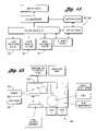
- FIG. 1is a schematic block diagram showing some elements of a laser processing system corresponding to one embodiment of the present invention wherein a microtextured pattern is formed on a workpiece, for instance, to form indicia on a portion of a semiconductor wafer;
- FIG. 2is a schematic block diagram showing some elements of a laser processing system corresponding to one embodiment of the present invention wherein a microtextured pattern, which may be formed with the system of FIG. 1 a , is further processed with a secondary beam, for instance to erase a mark;
- FIGS. 3 and 4illustrate some details of first and second sides of semiconductor wafer, an example of a workpiece which may be processed with various embodiments of the present invention
- FIG. 5is a schematic illustrating an exemplary microtextured region which may be formed with a femtosecond laser system
- FIGS. 6 and 7are schematics comparing prior art marks with marks formed in accordance with the present invention, and illustrate improved density of a dot matrix pattern
- FIGS. 8 and 9are schematics comparing prior art marks with marks formed in accordance with the present invention, and illustrate improved density of a bar pattern
- FIGS. 10 and 11are schematics illustrating, by way of example, a prior art laser mark formed on a specular surface, for instance bare silicon, and a corresponding surface profile showing exemplary defects associated with a deep (“hard”) mark—for instance slag and melted zones, debris, and microcracking;
- a deep (“hard”) markfor instance slag and melted zones, debris, and microcracking
- FIGS. 12 and 13are schematics illustrating, by way of example, a mark formed on the specular surface of FIG. 10 using a system of the present invention and an exemplary profile for comparison with FIGS. 10 and 11 ;
- FIGS. 14 and 15are schematic block diagrams showing some elements of a semiconductor wafer processing system
- FIGS. 16 and 17illustrate subsystems of a semiconductor wafer processing system corresponding to FIGS. 14 and 15 in further detail;
- FIGS. 18 and 19show some components of an exemplary laser beam positioning system which may be included in FIG. 1 or FIG. 2 for practicing various embodiments of the present invention
- FIG. 20is a schematic block diagram, similar to FIG. 16 , showing some elements of a semiconductor wafer processing system, specifically, elements related to secondary processing of FIG. 2 ;
- FIGS. 21 and 22illustrate the structure of various laser marks produced with conventional and more recent laser marking systems for further comparison with a marks formed in accordance with the present invention
- FIG. 23illustrates removing material, for instance, erasing a mark using a secondary processing beam corresponding, for example, to FIG. 2 ;
- FIG. 24illustrates removing material, for instance, modifying a microtextured pattern, using a secondary processing beam corresponding, for example, to FIG. 2 ;
- FIGS. 24-37 dillustrate various examples and results wherein silicon wafers having ground, polished, smooth, or rough surfaces are marked in accordance with the present invention.
- Ultrafast laseror “ultrashort laser” generally refers to a pulsed laser providing one or more pulses, each pulse having a duration below 1 ns, for instance 100 ps or less, or typically less than 10 ps;
- Microtexturegenerally refers to micron sized surface variations, but may also include surface variations of a finer scale, for instance 0.5 microns or 0.1 microns;
- “Nanotexture”generally refers to surface variations below one micron in size.
- New laser marking technologyhas been developed to overcome limitations of present laser marking systems. Permanent and high contrast shallow marks (less than 1 micron) on the backside of wafers are achieved with little or no material removed by using this new laser technology. Viewing of these marks is strongly independent of the viewing angle, a significant advancement.
- the so-called micro marking technologyallows the mark font size to be much less than 0.3 mm.
- At least one embodiment of the inventionmay be applied to micro machining of fine, laser-marked patterns.
- One or more embodiments of the inventionmay be applicable to laser micro assembly techniques for silicon articles including laser welding and laser actuation of micro device members.
- One aspect of the inventionfeatures a method of marking a material of a microelectronic device with a pulsed laser output to form high-density, discernible indicia on the material.
- the methodincludes: generating a pulsed laser output having at least one pulse with a pulse duration less than about 1 ns and having total fluence sufficient to initiate ablation of a portion of the material, the fluence being measurable over a spatial spot dimension of the output.
- the methodfurther includes directing the laser output in response to at least one control signal that defines a first location of at least a portion of indicia to be formed on the material, to impinge a localized region of the material at the first location, the localized region being within the spatial spot dimension.
- the laser outputinitiates ablation of at least a portion of the material and substantially increases surface roughness within at least the portion of the region.
- the region and background material that proximately surrounds the regionare both substantially slag-free.
- a background surfacemay have a strong specular reflection component.
- the diffuse reflectance of the indiciamay be in a range of 0.5% to 5%.
- the total fluencemay exceed about 0.1 J/cm 2 .
- the laser outputmay have a wavelength less than an absorption edge of the material.
- the laser wavelengthmay be ultraviolet.
- the pulse durationmay be in the range of about 15 fs to 500 ps.
- the pulse durationmay be in the range of about 100 fs to 50 ps.
- the pulse durationmay be in the range of about 300 fs to 15 ps.
- the materialmay be silicon.
- the materialmay be a metal or dielectric.
- the materialmay be a portion of a dielectric passivation layer, and the dielectric may be inorganic, organic, or a Low-k dielectric.
- the materialmay be part of a MEM device.
- a portion of the indiciamay have surface height variations in the range of about 0.25 microns to about 1 micron.
- a feature dimension of the indiciamay be in the range of several microns to tens of microns.
- a feature dimension of the indiciamay be a few optical wavelengths.
- the marking systemincludes: means for generating a pulsed laser output having at least one pulse with a pulse duration less than about 1 ns and having total fluence over a spatial region of the output sufficient to initiate ablation of a portion of a material to be marked; a controller that accepts data that define indicia to be formed on a material of a microelectronic article and produces at least one position control signal to direct a laser output to mark the material and thereby form the indicia; and means for directing the laser output to a surface location of the material to be marked so as to form discernible, high contrast, high-density indicia on the material surface.
- the means for directingmay include an optical scanner.
- the means for directingmay include a positioning subsystem for positioning the material relative to the laser beam in three dimensions.
- the positioning subsystemmay have three or more degrees of freedom.
- the optical scannermay be a two-dimensional, galvanometer-based scanner.
- the means for directingmay include an X-Y stage and a beam deflector coupled to the controller.
- the position control signalmay be produced during at least one step of manufacturing the article.
- the means for generatingmay includes a seed laser and a fiber optic amplifier.
- the means for generatingmay include a frequency doubled, diode-pumped, solid-state laser.
- the means for generatingmay include a mode-locked oscillator, a diode-pumped, solid-state laser amplifier, and a wavelength shifter.
- the means for generatingmay include a frequency doubler, frequency tripler or frequency quadrupler.
- the laser outputmay have a repetition rate greater than 10 KHz.
- the average laser output powermay be in the range of 0.01W-2W.
- the systemmay further include a viewing system for reading the indicia, including an illuminator and an electronic imaging system.
- the illuminatormay be bright-field.
- the illuminatormay be dark-field.
- the illuminatormay be a combination of bright and dark field.
- the articleincludes at least one material having discernible indicia formed on the material during at least one step of manufacturing the article.
- the indiciaare formed by a method of selectively irradiating at least one localized material region with a pulsed laser output.
- the indiciaare at least semi-permanent and useable during a subsequent step of manufacturing the article.
- a marked region and background material that proximately surrounds the regionare both substantially slag-free.
- the surface roughnessis increased within at least a portion of the material region, and thereby reduces reflection of energy used for reading the indicia.
- the method of selectively irradiating at least one localized material region with a pulsed laser outputis the above section entitled “Laser Marking/Texturing Method.”
- High reflectance contrastmay be obtained between the region and the background over a wide range of viewing angles.
- a background surfacemay have a strong specular reflection component.
- Reflectance contrast between the discernible indicia and the backgroundmay exceed 30:1 over an angular viewing range of at least 20 degrees.
- the indiciamay include an alphanumeric indicium having font dimension 0.3 mm or finer.
- the indiciamay include a two-dimensional matrix code.
- the indiciamay be useable for one or more manufacturing steps in addition to identification.
- the indiciamay be distinguished from the background with a roughness measurement obtained by at least one of SEM (scanning electron microscope) data, and AFM (atomic force microscope) data.
- DIN 4768 roughness measurement standardsmay be utilized to compare the roughness of a portion of the indicia with the background.
- the indiciamay be distinguished from the background with a measurement of image contrast.
- the indiciamay be machine readable.
- the indiciamay appear as a sequence of non-overlapping dots that form a dot matrix code.
- the indiciamay be used in at least one of traceability, component identification, and sorting.
- Embodiments of the present inventionmay be used to form indicia on ground, polished, or smooth material surfaces, based on specific application requirements.
- a surfacemay be coated.
- the surfacemay be either side of a semiconductor wafer, or another material used in a step of fabricating a microelectronic device.
- an ultrafast laser source 102 of a laser processing systemgenerates a laser output 104 which includes one or more pulses.
- the laser output 104propagates through delivery optics 106 that focus the output and deliver the beam into a process chamber 110 , the chamber 110 being used if the laser processing is to be carried out in a gaseous environment.
- the process chamber 110may contain a gaseous processing environment at a pressure, partial vacuum, or temperature as is known in the field of laser material interaction to produce microtextured silicon. For processing in ambient, atmospheric conditions the chamber is not required.
- the focused beam 108produces a working spot 112 that is incident on the target material, which may be a portion of a silicon semiconductor wafer 114 , and produces marked material 116 (not to scale).
- the wafer 114may have a bare (unpatterned) backside 117 , which may be coated, polished, or rough. Fiducials 118 are used for alignment.
- the topside shown in FIG. 3may have a large number of die 119 and corresponding dense circuit patterns.
- An optional secondary laser processing systemmay be used for further processing.
- a second laser source 120to erase, micromachine, weld, or actuate the region of the mark, a second laser source 120 generates a secondary beam 122 .
- High absorption within the marked regioncan support such further processing.
- the actuationmay occur as a result of differential thermal expansion of the material and background subsequent to heating the material with the secondary processing beam.
- the beam 122propagates through secondary delivery optics 124 that focus the beam.
- the secondary laser source 120may be a pulsed, modulated, or CW source, depending on the application.
- the focused beam 126produces a secondary working spot 130 that is incident on the wafer 114 and irradiates the marked material 116 .
- the irradiationmay be below the ablation threshold of the marked material to heat the region for actuation or above the threshold to effect material property changes.
- the two laser systems 100 , 129 having beam paths 104 , 122may be included in separate systems, or the optical systems may be combined by various well-known methods into a single laser system. There may be two optical axes, one for each beam path, or the beam paths may be combined for a coaxial beam path.
- a single laser headmay produce the beams of the laser sources 102 and 120 , or there may be two laser sources.
- the secondary laser 120has a wavelength near or exceeding the absorption edge of silicon.
- the choice of integrating into a single systemmay be based on specific design considerations, for example, workpiece dimensions, laser wavelengths and power, optical design considerations, component costs, available factory floor space, X-Y positioning requirements, etc.
- the delivery systems 106 and 124corresponding to the texturing system 100 and the secondary processing system 129 , respectively, will often include some elements operated under computer control, as indicated by lines 107 and 127 , respectively. For example, focusing, spot size adjustment, polarization control, and energy control functions may be controlled. Suitable combinations of electro-optic devices, modulators, and opto-mechanical devices for positioning may be utilized. For instance, either delivery system 106 or 124 may include a polarization controller to enhance or control a mark characteristic.
- the ultrafast laser 102may produce one or more femtosecond pulses.
- picosecond lasersmay provide many of the benefits of femtosecond lasers but at reduced cost and complexity.
- Controlled laser-material interaction at the ultrafast scalecan be used to control the contrast of the marks over a wide range to meet specific application requirements. Of further significance is the reduction or elimination of debris, slag, cracking, and other undesirable effects generally associated with traditional marking lasers.
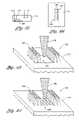
- FIG. 5illustrates an exemplary “spiky” textured region 135 with the surface height 136 illustrated by a typical spike.
- the spikesmay have a height ranging from a fraction of one micron to tens of microns.
- the surface profilemay be strongly dependent on laser parameters including pulse duration (i.e., width), peak energy, spot diameter, and spot irradiance profile.
- Embodiments of the present inventioncan be used to create microtextured regions having lower amplitude (e.g., sub-micron) surface height variations than exemplified in the above paragraph, but with sufficient variations to create high contrast, slag-free marks. Further, enhanced contrast and absence of debris provides for improved mark density when compared to traditional marking approaches.
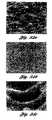
- FIGS. 10 and 11are schematics illustrating, by way of example, a prior art laser mark formed on a specular surface, for instance bare silicon, and a corresponding surface profile showing debris and cracking associated with a deep, “hard” mark.
- FIGS. 12 and 13are schematics illustrating, by way of example, a mark formed on the specular surface of FIG. 10 using a system of the present invention.
- the pulsed lasermay be a picosecond laser producing a pulsed output with total energy density (in one or more pulses) sufficient to initiate ablation within a portion of a spot area on the substrate surface.
- the surface height variationsmay be tens to hundreds of nanometers, the marked region generally showing significant roughness and eliminating at least strong reflection components.
- FIGS. 6 and 7are schematics comparing prior art marks with marks formed in accordance with the present invention, respectively, and illustrate improved density of a dot matrix pattern.
- FIGS. 8 and 9are schematics comparing prior art marks with marks formed in accordance with the present invention, respectively, and illustrate improved density of a bar pattern.
- FIGS. 21 and 22illustrate the structure of various laser marks produced with traditional and more recent laser marking systems for further comparison with a marked substrate produced in accordance with the present invention.
- FIGS. 21 and 22respectively, are side and top schematic views of a mark 250 formed by the assignee of the present invention using a NdYVO4 laser with a pulse width of about 15 ns at 532 nm. The laser system produced shallow marks having a depth of about 1.5-4 microns without substrate cracking.
- FIG. 22is a top view of a mark 250 illustrating the presence of ejected material 252 adjacent to the mark 250 .
- FIG. 21is a side schematic view of a relatively deep traditional “hard” mark 254 , about 10 microns in depth, wherein cracking of silicon is observed with relatively deep, laser penetration 256 .
- these textured (marked) areas formed in accordance with the present inventionprovide high contrast relative to the reflective wafer background surface 115 .
- the wafer surface 115may be smooth relative to a visible wavelength, thereby resulting in a strong specular reflection component with negligible diffuse reflection.
- a textured regionmay appear opaque, and will preferably have diffuse reflectance corresponding to the darkest shades of “grey scale charts” used for calibrating imaging systems.
- the diffuse reflectancemay be in a range of about 0.5% to 5%, corresponding to about 6 shades of grey.
- the contrastprovides detection for improved-detection, machine-readable marks such as alphanumeric strings, bar codes, matrix codes, etc.
- Such indiciamay be viewed with a mark inspection system 201 , which may be one component of a complete laser processing system as shown in FIG. 14 which, by way of example, includes both the marking laser system 100 , and-the secondary laser processing system 129 of FIGS. 1 and 2 , respectively.
- the system 129may be used to erase a mark.
- a systemmay include only laser marking and an optional mark inspection system 201 without secondary processing.
- With an ultrafast (or ultra-violet) sourceshallow marks with highly controllable depths are possible that would be advantageous for marking or coding very thin wafers, for instance, with mark dimensions substantially finer than present commercially available systems.
- a following section entitled “Marking Examples” and referenced drawing figuresshow exemplary results using picosecond lasers to produce laser marks on silicon substrates having rough, ground, or smooth surfaces.
- the readability of the marksis improved over conventional laser marks.
- the marksappear substantially opaque and the contrast with the background remains high as a function of illumination and viewing angles, for instance, as the relative angle between an illumination source and receiver is varied over 30 degrees. This invariance increase the reliability of machine vision algorithms.
- Various embodiments of the inventionprovide for high contrast marks on wafers and marks on other microelectronic articles or devices made from silicon. Further application is expected to MEMS and MOEMS devices and for providing marks or other patterns on materials such as Ti and steel.
- the markingmay be used primarily for identification, or it may be used to change the material's optical properties at discrete sites for functional or subsequent process reasons.
- wafers to be processedare removed from a wafer carrier by a robotic wafer handling system 205 , as illustrated schematically in FIGS. 14 and 15 .
- Orientation of the waferis determined by optical alignment, including operation of a pre-aligner 206 and any other required steps, for instance identifying the wafer type with a reader 207 .
- the laser 102generates a processing beam.
- the beam positioning system 106delivers and focuses the ultrafast processing beam onto a workpiece, which may be a silicon substrate. Interaction of the focused processing beam with the material of the workpiece in an atmosphere or ambient environment creates microtexture on the surface of the workpiece.
- Laser pulses 104(i.e., FIG. 1 ) generated by the ultra-short pulse laser 102 propagate along the optical path 104 , and are deflected or otherwise positioned with a beam positioner 220 ( FIG. 16 ).
- the beam positioningwill typically be carried out using two galvanometer scan mirrors which generally provide for deflection over a wide angle with a scan lens used to focus the output onto the wafer 114 which is typically mounted on an X-Y stage 208 .
- Each laser pulse (or pulse sequence)forms a microtextured spot of material on the wafer 114 .
- the positioning of the beamis determined by a controller so that a sequence of laser pulses forms characters or other indicia on the wafer 114 .
- the wafer 114is removed from the processing area and reloaded into its wafer carrier.
- a secondary processing stepmay occur with the system 129 before the wafer 114 is transferred.
- Relative controlled movement of the workpiece and the focused processing beamselectively creates microtexture that forms discernible patterns on the workpiece.
- top-hat irradiance profile spotscan provide indicia with more uniform microtexturing and reduced melting at the ablation threshold transition zone.
- the area of the spot at or above the ablation thresholdcan be increased without an increase in the pulse energy, thereby efficient microtexturing is achieved. It may be desirable to use a spot with a depressed center and energy concentrated in the perimeter to further limit melting and increase sharpness of the microtexture substrate transition at the kerf edge.
- Round spotsprovide consistent exposure for line elements in any orientation. However, square and rectangular spots can further increase efficiency and uniformity by delivering a uniform dose across an aligned kerf width and to larger areas requiring filling.
- Control of the aspect of a spotcan be used to precisely control the irradiance and spot overlap. For example, maximum pulse energy may be selected and spot length along a trajectory may be expanded or contracted to modify the shape of the area exposed at or above the ablation threshold.
- the spotmay be expanded to expose a larger area at or above the ablation threshold without increasing the kerf width or can allow the kerf width to be reduced without increasing irradiance.
- the spotmay be expanded to allow expose of at least a portion of the spot to an increased number of laser pulses.
- compression of the spot along the kerfmay be used to increase the exposure to or above the ablation threshold without decreasing the kerf width or can allow the kerf width to be increased without decreasing irradiance. Compression of the spot may also be used to allow exposure of at least a portion of the spot to a decreased number of pulses.
- the lasermay be an ultrafast laser.
- the ultrafast lasermay have a wavelength below the absorption edge of the substrate, for example 532 nm for silicon processing.
- the average power, which relates to the required threshold fluence and repetition ratemay be in the approximate range of 0.01W-2W for marking silicon wafers using various embodiments of the present invention.
- the pulse width (duration)may be less than 1 ns.
- the laser pulse widthwill be in the range of about 100 fs to about 50 ps, and most preferably in the range of about 300 fs to 10 ps.
- Certain embodimentsmay use a diode-pumped, solid-state UV laser with a pulse width less than about 20 ns, and preferably less than 1 ns. Formation of the desired microtexture may utilize gas-assist or a gaseous environment in the chamber 110 , as shown in FIG. 1 , for best results with UV processing.
- FIGS. 16-19show additional details of an exemplary laser processing system which may be used for laser marking of substrates, for instance marking of silicon wafers (front and/or backside).
- a positioning subsystemmay include one or more translation stages 208 for moving the workpiece relative to the processing beam 108 along at least two axes.
- Numerous combinations of relative substrate and beam positioning devicesare known to those skilled in the art of laser material processing, for instance, semiconductor processing, stereolithography, semiconductor laser repair, laser drilling, or semiconductor wafer trirnming.
- FIGS. 7 and 9are typically tens of microns in commercially available marking systems.
- a laser marking system of the present inventionmay be used to produce significantly smaller feature sizes, for instance 5-10 micron dots.
- the features in FIGS. 7 and 9may be characterized by a minimum resolvable distance between features of the pattern. The minimum resolvable distance may be on the order of a wavelength of the pulsed laser output, for instance 0.25 microns.
- the positioning systemmay include fine and coarse positioners to match or exceed the pattern resolution and provide for ultra-fine patterning.
- the fine stagemay have a travel range on the order of millimeters positioning accuracy substantially finer than 1 micron, for instance 0.05 microns.
- the systemmay also include other auxiliary fine positioners, for instance precision, small-angle, beam deflectors (e.g., an acousto-optic deflector), together with closed loop control.
- auxiliary fine positionersfor instance precision, small-angle, beam deflectors (e.g., an acousto-optic deflector), together with closed loop control.
- Such positioning systemsmay be used in embodiments of the present invention for laser marking, patterning, joining, or other applications.
- embodiments of the invention for practicing laser marking and other applications with laser systems 100 , 129may include irradiating first and second sides of the workpiece.
- wafer chuck 249may be mounted to an X-Y stage in a configuration suitable for laser systems 100 , 129 to irradiate opposite sides of the workpiece surface.
- the wafer chuck 249may include a Z-axis translator and capability for tilting the workpiece (rotation about the x-y axes). Such precision translation and rotation stages have been applied in lithography, laser trimming, and similar applications.
- either or both beam positioning systems 220 , 220 ′may include a two-axis, galvanometer-based, beam scanner 240 , 242 to move the beam relative to the workpiece.
- Either beam positioning system 220 , 220 ′may include a combination of two or more stages and scanners to move the processing beam relative to the workpiece in at least two axes.
- components to position the beam waist relative to the workpiece through movement 246 of one or more optical elements within the secondary laser systemmay be included.
- componentsmay be included to move the beam waist relative to the workpiece in at least 3 axes using various combinations of movement 246 of optical system components with z-axis translation 246 ′ using, for example, a motorized wafer chuck assembly.
- Precision galvanometric scanning heads 240 , 242are available from GSI Lumonics Corporation (assignee of the present invention), Cambridge Technologies and Scan Labs LTD. Exemplary options for an associated optical system are illustrated in FIGS. 18 and 19 include: (1) a telecentric lens or f-theta corrected lens 221 with programmable spot size adjustment 222 ; and (2) a widefield post-objective system 223 and motorized dynamic focus adjustment 224 (not shown in FIG. 16 ).
- the focusing subsystem 106 in the ultrafast systemis illustrated as a refractive optical system.
- an all reflective systemmay provide for improved performance as a result of dispersion compensation.
- an ultrashort pulsemay have a wavelength spread of about 8 nm or more about the central wavelength.
- Femtooptics, Inc.is a supplier of femtosecond optical components.
- Extremely high absorption microtexturesmay be produced in a non-ambient atmosphere, with processing carried out in a processing chamber.
- the processing atmospheremay containing gases or may be a vacuum to assist the formation of microstructures.
- microstructuresare formed in a open atmosphere of gases, and it is most preferred that the workpiece is placed in ambient air.
- the microtexture createdreduces reflected energy off the surface of the workpiece.
- the microtexture createdis spike or cone-like structures, on the order of or smaller than the wavelength of light, the surface profiles of which are illustrated in FIG. 5 as an exemplary regular arrangement and FIGS. 12 and 13 as a microtextured region with reduced height variation (peak amplitude) and regularity.
- Very highly absorbing structureshave been made in process chambers.
- moderately absorbing structurese.g., FIGS. 12 and 13
- FIGS. 12 and 13are considered for various embodiments of the present invention, thereby reducing the system requirements needed to create the microtextured regions.
- the patterns formedmay be alpha-numeric characters.
- the patterns formedmay be logotypes.
- the patterns formedmay be machine-readable.
- the patternsmay be also be human-readable.
- a font size of finer than 0.3 mmis achievable using one or more embodiments of the present invention.
- the systemmay include an integral mark inspection system 201 (i.e., FIG. 14 ) to identify the patterns, or the inspection may be included in a separate system or station of a manufacturing process.
- an integral mark inspection system 201i.e., FIG. 14
- machine vision technologyfor instance pattern recognition systems supplied by Cognex, Inc. may be used for mark identification.
- pattern recognition systemssupplied by Cognex, Inc.
- laser-based microtexturinghas produced high contrast marks, relatively insensitive to illumination conditions, including camera angle and lighting angle over a wide range.
- the inspection vision system 201may be implemented (or replaced) with an optional “though the lens” vision system configuration integrated within a galvanometer system, for instance designs corresponding to FIGS. 18 and 19 .
- the substrate materialmay be a metal, a silicon wafer (bare or with various coatings).
- Other exemplary materialsinclude inorganic or organic dielectrics (including low-k materials, metallization, refractory metals, and plastics).
- the material to be markedmay be part of a multimaterial device, which may include a layer of silicon dioxide on silicon, for instance.
- the materialmay be an inorganic or organic dielectric, for instance a passivation layer.
- the marked areasmay be permanent, semi-permanent, or erasable so as to be utilized in the process of making the multimaterial device, for instance, to control or select various fabrication steps.
- Exemplary devicesinclude a multimaterial semiconductor memory, damascene structure, processors, peripheral chips, etc., RFID tags, MCMs, and the like.
- an ultra-short pulse laser sourceis to be included within a commercially soft-mark type of wafer marking system such as the GSI Lumonics WaferMark SigmaClean. Details regarding various laser system alternatives are included in a later section.
- the soft marks normally created in the wafer marking systemare replaced with shallow, low-reflectance, angle-insensitive marks.
- Integration of the ultra-short pulse laser sourcerequires mechanical and optical changes to couple the laser energy into an optical path of the machine, propagate the beam along the optical path and focus the beam onto the substrate. The integration may be carried out by design practices well-known to those skilled in the art of designing laser beam processing systems.
- a highly absorbing marked areamay be irradiated for subsequent processing according to various methods of this invention.
- the secondary irradiationmay use lasers that are more weakly absorbed in the substrate, for instance lasers that operate near or beyond the absorption edge of silicon.
- lasersthat are more weakly absorbed in the substrate
- Various studieshave shown increased absorptance within the microtextured regions both in the visible and the NIR. Near and beyond the absorption edge of silicon, high power processing lasers can be used with minimal damage to the normally transmitting substrate.
- the first ultrafast stepmay produce fine patterning that is processed with a coarse secondary beam, and conversely, the first step may produce a coarse mark that is finely patterned with the secondary step.
- the absorbing materialmay be ablated in a micromachining step with controlled depth.
- this ablationmay be for the purpose of removing or erasing 410 the mark, creating a negative “window” mark on an absorbing field, or it may be to micromachine a fine pattern, or trim an electrical or mechanical parameter.
- FIG. 24shows a microtextured area that is modified at 420 with secondary irradiation 126 .
- the operations to produce the microtextured regionmay be carried out within a system as illustrated in FIG. 14 , or at a different location in the manufacturing process.
- FIGS. 2 and 20illustrate several components which may be used in a secondary processing system and these system components may be similar or identical to those used in the ultrafast system.
- the laser 120generates the secondary processing beam.
- a beam positioning systemwhich may correspond to any suitable arrangement of optical or mechanical beam positioners, delivers and focuses the secondary processing beam 126 onto a microtextured area of a workpiece.
- the secondary laser energyis absorbed by the microtexture.
- the microtextureis heated and the increased temperature is sufficient to cause a phase change in the material.
- the secondary processing laser 120may be a YAG or CO2 laser.
- the laser 120is selected to minimize damage to non-microtextured areas.
- the laser beam 126is transmitted through the non-microtextured material.
- the preferred wavelengthmay be about 1.2 microns (e.g., using a Raman laser) where the silicon transmission is generally maximized.
- a commercially available 1.32 micron lasermay also be nearly optimum, and such lasers are widely available.
- the beam positioning systemmay include one or more stages 208 for moving the workpiece relative to the processing beam, in an arrangement similar or identical to FIG. 20 .
- the beam positioning systemmay include a beam scanner 240 , 242 to move the beam relative to the workpiece and a focusing lens.
- the specific choice of components and other featureswill generally depend on the laser wavelength, spot size requirements, damage threshold considerations, etc.
- the beam positioning systemmay include a combination of two or more stages and scanners to move the processing beam relative to the workpiece in at least two axes.
- the beam positionermay position the beam waist relative to the workpiece through movement 246 of one or more optical elements within the secondary laser system.
- the beam positioning systemmay move the beam waist relative to the workpiece in at least three axes.
- the beam positioning systemmay move the beam waist relative to the workpiece in at least three axes using various combinations of movement of optical system components with z-axis translation 246 ′ using, for example, a motorized wafer chuck assembly.
- the microtextured areamay be formed according to an embodiment of the current invention, but is not restricted to ultrashort laser processing. Generally, the microtextured area is to decrease the reflection coefficient of the workpiece material.
- the irradiated materialmay be ablated from the surface to remove the absorbing structure.
- the irradiated materialmay be melted and recast to form an area with modified properties.
- the secondary beammay have a wavelength which corresponds to maximum transmission through the non-textured material.
- the non-textured regionis also silicon
- the secondary beammay have a wavelength beyond the absorption edge of silicon, for instance greater than 1.2 microns.
- the wavelengthmay be in the visible or near IR region. In some applications it may be desirable to use a laser that is absorbed in the microtexture and the adjacent material
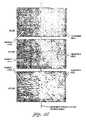
- FIGS. 25 to 36relates to actual results obtained using a commercially available picosecond laser to form marks on silicon substrates having ground, polished, or smooth surfaces.
- Laser and system parameters for some marked regionsare as follows:
- Silicon wafer(with mark on specular surface);
- Silicon wafer(with mark on rough surface);
- Silicon wafer(with 15 line mark within 0.28 mm);
- the sampleswere mounted on X-Y stage, and the mark linewidth was varied by adjustment of a combination of the optical system and incident laser energy, the adjustments controlling the energy density incident on the material.
- the images of the marked material sampleswere taken using a “through the lens” (brightfield) microscope system and CCD camera. Various regions were profiled using either a SEM (scanning electron microscope) or AFM (atomic force microscope). Certain marks were also compared with marks formed using a nanosecond laser system.
- the number of pulses corresponding to a particular linewidthcan be computed from the pulse repetition rate, linewidth, and table speed. For instance, FIG. 25 corresponds to 34 applied pulses during stage travel corresponding to the linewidth of 115 ⁇ m.
- the listed laser parameters and resultsare to be regarded as exemplary rather than limiting.
- the laser parametersmay be optimized or adjusted based on various process conditions, surface roughness figures, presence/absence of coatings, etc. Various refinements and adjustments may provide for further improvements in contrast and density.
- the linewidthcorresponds to an effective spot size on the surface wherein the fluence is at or above an approximate ablation threshold of silicon. Hence, if a greater fraction of the spot is above the ablation threshold the linewidth increases. For example, if the spot profile is diffraction limited and Gaussian and the region above threshold corresponds to the FWHM, then the nominal kerf width will be approximately the FWHM.
- the laser used in the experiments and general laser system specificationsare as follows:
- FIGS. 25 , 26 and 27show marks formed on a ground silicon substrate, exemplified by the grind direction (as opposed to uniform, specular background).
- FIGS. 26 and 27provide a rough test of the “process energy window” which represent the energy range over which acceptable processing is achieved.
- the larger linewidth (140 microns) in FIG. 26corresponds to a larger fraction of the focused spot diameter above the ablation threshold.
- a slight heat-affected zone (HAZ)is shown in the regions where melting occurs, though insignificant. Undesirable slag, debris, or severely melted zones are absent.
- FIGS. 28 and 29show parameters and results where a 40 micron linewidth was produced in the X and Y directions, respectively.
- the polarizationwas perpendicular to the direction of travel.
- FIGS. 30 a , 30 b , 31 a , 31 b , 32 a , 32 b and 32 cillustrate improved mark density and a clearly resolved pattern within a 0.3 mm (0.28 mm) region, a result which demonstrates capability to form finer indicia than available in current, commercially-available, laser marking systems.
- FIG. 30 a and 30 bcorrespond to a specular wafer background (smooth finish)
- FIGS. 31 a and 31 bcorrespond to a rough back-side wafer surface
- FIGS. 32 a , 32 b and 32 ccorrespond to a polished wafer.
- the enlarged photosprovide some local additional detail, the definition and sharpness reduction believed to be caused by various limitations in the setup, for instance the camera dynamic range, the high N.A. of the microscope collecting additional scattered light, and other factors.
- the high contrast imagescorrespond to the approximate magnification to be used by a typical mark reader/inspection system.
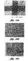
- FIGS. 33 a and 33 bcompare a high contrast mark obtained with the picosecond system (i.e., FIG. 33 a ) with a mark formed with a typical nanosecond laser-based marking system (i.e., FIG. 33 b ).
- the nanosecond “dark” mark surface roughnessis not significantly altered, whereas the microtexture is formed only within the picosecond mark.
- FIGS. 34 a , 34 b and 34 cshow SEM images of the marked regions further demonstrating the presence of the microtexture produced with the picosecond system as follows:
- the nanosecond resultsshow only insignificant roughness (“dark mark” case), the surface roughness variations evident with the picosecond results were not detected in the nanosecond data—neither the “dark” or “hard” marks show the microtexture.
- the deep markstraditional “hard marks” also show highly undesirable ridge formations. Of significance is an observation that even for “dark” nanosecond marks (which are relatively shallow compared to “hard marks”), the microtexture is not detected in the images corresponding to the nanosecond marking.
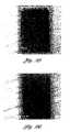
- FIG. 35shows SEM images obtained from a marked region of a polished wafer.
- a surface regionis shown at three SEM magnifications: 15,000X, 6,000X, and 25,000X.
- the texture boundary between the marked and unmarked regionis evident, even with the polished background variations. Further, the marked region, its periphery, and the polished background are all slag-free—ridges and kerf height negligible.
- FIGS. 36 , 37 a , 37 b , 37 c and 37 dshow measurement of a marked region of a polished wafer using an AFM to measure surface heights. Sub-micron structures are evident, with peak heights in the range of tens to hundreds of nanometers.
- the polished background regionscorrespond to the semi-specular, strong directional reflectance results shown in earlier figures. A very high contrast is achievable for specular wafer backgrounds providing for clear recognition of textured and non-marked specular wafer regions. In such a case, the indicia may also be clearly distinguished from the background using AFM or SEM measurements which will exemplify the difference in texture.
- the examplesgenerally show marked regions which have roughness greater than a reflective background.
- This examplemay be of interest if, for example, the system throughput is not degraded (or is improved) using the technique (e.g., wherein the total area of the indicia is to be greater than the background area).
- certain applicationsmay require such “reverse contrast” as part of customer specifications.
- Other similar variations and alternativescan be carried out without departing from the scope and spirit of the present invention.
- the commercially available laser used to produce the high contrast results of the above working exampleincludes a mode locked oscillator and a diode pumped solid-state laser amplifier. Picosecond outputs are available with pulse parameters within a desired range.
- the choice of a laser systemis generally based upon the requirements for pulse energy, repetition rate, average power, pulse width required to irradiate the material to be marked with total energy density sufficient to initiate ablation within the spatial spot size on the material surface.
- Useful laser wavelengthsinclude near IR, visible (e.g., 532 nm), and ultraviolet. Other factors include size, cost, reliability, and various practical considerations for use in semiconductor production environment, for example.
- An “off-the-shelf” solutionis desirable when available.
- the laser systemis compatible with available marking equipment, for instance the commercially soft-mark type of wafer marking system such as the GSI Lumonics WaferMark SigmaClean.
- the laser systems of the above-noted incorporated patent applicationsmay be modified for use at shifted wavelengths (e.g., green and UV).
- the system outputfor instance average power and peak energy, may be adjusted to meet the energy density requirements with reduction or increase or amplifier gain as needed to process at a required energy density.
- FCPA systemFiber based Chirped Pulse Amplification
- FCPA Americaincludes 2 microjoules of pulse energy at a repetition rate of 500 KHz, corresponding to 1W average power operation at femtosecond pulse widths.
Landscapes
- Engineering & Computer Science (AREA)
- Physics & Mathematics (AREA)
- Optics & Photonics (AREA)
- Mechanical Engineering (AREA)
- Plasma & Fusion (AREA)
- General Physics & Mathematics (AREA)
- Microelectronics & Electronic Packaging (AREA)
- Condensed Matter Physics & Semiconductors (AREA)
- Computer Hardware Design (AREA)
- Power Engineering (AREA)
- Theoretical Computer Science (AREA)
- Chemical & Material Sciences (AREA)
- Materials Engineering (AREA)
- Manufacturing & Machinery (AREA)
- Laser Beam Processing (AREA)
Abstract
Description
- Wavelength 532 nm;
- Repetition rate 30 KHz;
- Average power 460 mw;
- 15 μj pulse energy;
Linear mark speed 100 mm/sec;Line width 115 μm;- Energy density 0.15 J/cm2;
- Peak power density 1010W/cm2;
- Overlap: 34.
- Wavelength 532 nm;
- Repetition rate 30 KHz;
- Average power 500 mw;
- 16.3 μj pulse energy;
Linear mark speed 100 mm/sec;- Line width 140 μm;
- Energy density 0.16 J/cm2.
- Wavelength 532 nm;
- Repetition rate 30 KHz;
Average power 300 mw;- 9.8 μj pulse energy;
- Linear mark speed 16.6 mm/sec;
- Energy density 0.1 J/cm2.
- Wavelength 532 nm;
- Repetition rate 30 KHz;
Average power 100 mw;- 3.3 μj pulse energy;
Linear mark speed 100 mm/sec;Line width 40 μm;- Energy density 0.26 J/cm2;
- Peak power density 1.7×10¹⁰W/cm2.
- Wavelength 532 nm;
- Repetition rate 30 KHz;
Average power 100 mw;- 3.3 μj pulse energy;
Linear mark speed 100 mm/sec;Line width 40 μm;- Energy density 0.26 J/cm2;
- Peak power density 1.7×10¹⁰W/cm2.
- Wavelength 532 nm;
- Repetition rate 30 KHz;
- Average power 7.2 mw;
- 0.24 μj pulse energy;
Linear mark speed 100 mm/sec;- Line width 8 μm;
- Energy density 0.12 J/cm2;
- Peak power density 0.8×10¹⁰W/cm2.
- Wavelength 532 nm;
- Repetition rate 30 KHz;
- Average power 7.2 mw;
- 0.24 μj pulse energy;
Linear mark speed 100 mm/sec;- Line width 8 μm;
- Energy density 0.12 J/cm2;
- Peak power density 0.8×10¹⁰W/cm2.
- Wavelength 532 nm;
- Repetition rate 30 KHz;
- Average power 7.2 mw;
- 0.24 μj pulse energy;
Linear mark speed 100 mm/sec;- Line width 8 μm;
- Energy density 0.12 J/cm2;
- Peak power density 0.8×10¹⁰W/cm2.
- Pulse width 15 ps;
- Wavelength 532 nm;
- Repetition rate 30 KHz;
- Average power (see attached results);
- Linear polarization;
- M-squared less than 1.2.
Claims (100)
Priority Applications (2)
| Application Number | Priority Date | Filing Date | Title |
|---|---|---|---|
| US11/514,660US7469831B2 (en) | 2004-06-30 | 2006-10-27 | Laser-based method and system for processing targeted surface material and article produced thereby |
| US11/801,706US20080073438A1 (en) | 2004-06-30 | 2007-05-10 | Laser-based method and system for processing targeted surface material and article produced thereby |
Applications Claiming Priority (3)
| Application Number | Priority Date | Filing Date | Title |
|---|---|---|---|
| US58426804P | 2004-06-30 | 2004-06-30 | |
| US11/152,509US20060000814A1 (en) | 2004-06-30 | 2005-06-14 | Laser-based method and system for processing targeted surface material and article produced thereby |
| US11/514,660US7469831B2 (en) | 2004-06-30 | 2006-10-27 | Laser-based method and system for processing targeted surface material and article produced thereby |
Related Parent Applications (1)
| Application Number | Title | Priority Date | Filing Date |
|---|---|---|---|
| US11/152,509DivisionUS20060000814A1 (en) | 2004-06-30 | 2005-06-14 | Laser-based method and system for processing targeted surface material and article produced thereby |
Related Child Applications (1)
| Application Number | Title | Priority Date | Filing Date |
|---|---|---|---|
| US11/801,706DivisionUS20080073438A1 (en) | 2004-06-30 | 2007-05-10 | Laser-based method and system for processing targeted surface material and article produced thereby |
Publications (2)
| Publication Number | Publication Date |
|---|---|
| US20080011852A1 US20080011852A1 (en) | 2008-01-17 |
| US7469831B2true US7469831B2 (en) | 2008-12-30 |
Family
ID=35512828
Family Applications (3)
| Application Number | Title | Priority Date | Filing Date |
|---|---|---|---|
| US11/152,509AbandonedUS20060000814A1 (en) | 2004-06-30 | 2005-06-14 | Laser-based method and system for processing targeted surface material and article produced thereby |
| US11/514,660Expired - LifetimeUS7469831B2 (en) | 2004-06-30 | 2006-10-27 | Laser-based method and system for processing targeted surface material and article produced thereby |
| US11/801,706AbandonedUS20080073438A1 (en) | 2004-06-30 | 2007-05-10 | Laser-based method and system for processing targeted surface material and article produced thereby |
Family Applications Before (1)
| Application Number | Title | Priority Date | Filing Date |
|---|---|---|---|
| US11/152,509AbandonedUS20060000814A1 (en) | 2004-06-30 | 2005-06-14 | Laser-based method and system for processing targeted surface material and article produced thereby |
Family Applications After (1)
| Application Number | Title | Priority Date | Filing Date |
|---|---|---|---|
| US11/801,706AbandonedUS20080073438A1 (en) | 2004-06-30 | 2007-05-10 | Laser-based method and system for processing targeted surface material and article produced thereby |
Country Status (6)
| Country | Link |
|---|---|
| US (3) | US20060000814A1 (en) |
| EP (1) | EP1779286B1 (en) |
| JP (1) | JP2008504964A (en) |
| KR (1) | KR101278433B1 (en) |
| AT (1) | ATE550132T1 (en) |
| WO (1) | WO2006012124A2 (en) |
Cited By (13)
| Publication number | Priority date | Publication date | Assignee | Title |
|---|---|---|---|---|
| US20080217309A1 (en)* | 2007-03-01 | 2008-09-11 | James Neil Rodgers | RFID antenna gain and range enhancement |
| US20100143744A1 (en)* | 2007-03-09 | 2010-06-10 | University Of Virginia Patent Foundation | Systems and Methods of Laser Texturing of Material Surfaces and their Applications |
| US20100219506A1 (en)* | 2005-12-21 | 2010-09-02 | University Of Virginia Patent Foundation | Systems and Methods of Laser Texturing and Crystallization of Material Surfaces |
| US20110053294A1 (en)* | 2009-08-31 | 2011-03-03 | Ulrich Mayer | Uv irradiance monitoring in semiconductor processing using a temperature dependent signal |
| US20120273472A1 (en)* | 2010-10-22 | 2012-11-01 | Electro Scientific Industries, Inc. | Laser processing systems and methods for beam dithering and skiving |
| US20120312781A1 (en)* | 2009-12-22 | 2012-12-13 | John Van De Sanden | Method of laser marking a bearing component with visually undetectable mark; bearing component with such marking; method of authentification such marking |
| US8846551B2 (en) | 2005-12-21 | 2014-09-30 | University Of Virginia Patent Foundation | Systems and methods of laser texturing of material surfaces and their applications |
| US20150209902A1 (en)* | 2010-10-21 | 2015-07-30 | Electro Scientific Industries, Inc. | Method and apparatus for optimally laser marking articles |
| US20150298260A1 (en)* | 2012-11-26 | 2015-10-22 | Akeo Plus | Method and system for marking a surface by laser treatment |
| US10131086B2 (en) | 2011-06-30 | 2018-11-20 | University Of Virginia Patent Foundation | Micro-structure and nano-structure replication methods and article of manufacture |
| US10391585B2 (en) | 2009-05-28 | 2019-08-27 | Electro Scientific Industries, Inc | Acousto-optic deflector applications in laser processing of dielectric or other materials |
| US11072109B2 (en) | 2013-09-20 | 2021-07-27 | Essilor International | Device and process for marking an ophthalmic lens with a pulsed laser of wavelength and energy selected per pulse |
| US20220127179A1 (en)* | 2018-02-06 | 2022-04-28 | Tesla, Inc. | Process to make textured glass |
Families Citing this family (117)
| Publication number | Priority date | Publication date | Assignee | Title |
|---|---|---|---|---|
| US7838794B2 (en) | 1999-12-28 | 2010-11-23 | Gsi Group Corporation | Laser-based method and system for removing one or more target link structures |
| US6951995B2 (en) | 2002-03-27 | 2005-10-04 | Gsi Lumonics Corp. | Method and system for high-speed, precise micromachining an array of devices |
| US7563695B2 (en)* | 2002-03-27 | 2009-07-21 | Gsi Group Corporation | Method and system for high-speed precise laser trimming and scan lens for use therein |
| US7015418B2 (en)* | 2002-05-17 | 2006-03-21 | Gsi Group Corporation | Method and system for calibrating a laser processing system and laser marking system utilizing same |
| US8653409B1 (en)* | 2004-06-23 | 2014-02-18 | Board Of Governors For Higher Education, State Of Rhode Island And Providence Plantations | Selective surface smoothing using lasers |
| US20060000814A1 (en) | 2004-06-30 | 2006-01-05 | Bo Gu | Laser-based method and system for processing targeted surface material and article produced thereby |
| US7705268B2 (en) | 2004-11-11 | 2010-04-27 | Gsi Group Corporation | Method and system for laser soft marking |
| US7466466B2 (en)* | 2005-05-11 | 2008-12-16 | Gsi Group Corporation | Optical scanning method and system and method for correcting optical aberrations introduced into the system by a beam deflector |
| GB0509727D0 (en)* | 2005-05-13 | 2005-06-22 | Renishaw Plc | Method and apparatus for scale manufacture |
| US7655003B2 (en) | 2005-06-22 | 2010-02-02 | Smith & Nephew, Inc. | Electrosurgical power control |
| FI20060358A7 (en)* | 2006-04-12 | 2007-10-13 | Picodeon Ltd Oy | Method for adjusting the ablation threshold |
| US7884323B2 (en)* | 2005-08-16 | 2011-02-08 | Cameca Instruments, Inc. | Atom probes, atom probe specimens, and associated methods |
| US9138913B2 (en)* | 2005-09-08 | 2015-09-22 | Imra America, Inc. | Transparent material processing with an ultrashort pulse laser |
| US7626138B2 (en)* | 2005-09-08 | 2009-12-01 | Imra America, Inc. | Transparent material processing with an ultrashort pulse laser |
| CN1958209A (en)* | 2005-11-03 | 2007-05-09 | 鸿富锦精密工业(深圳)有限公司 | Laser forming device |
| US20070117227A1 (en)* | 2005-11-23 | 2007-05-24 | Gsi Group Corporation | Method And System for Iteratively, Selectively Tuning A Parameter Of A Doped Workpiece Using A Pulsed Laser |
| US20070125863A1 (en)* | 2005-12-05 | 2007-06-07 | Jakoboski Timothy A | System and method for employing infrared illumination for machine vision |
| TWI504963B (en)* | 2006-01-30 | 2015-10-21 | Electro Scient Ind Inc | Achromatic scan lens |
| DE102006019118B4 (en)* | 2006-04-25 | 2011-08-18 | Epcos Ag, 81669 | Optical marking component and method of manufacture |
| US8198566B2 (en)* | 2006-05-24 | 2012-06-12 | Electro Scientific Industries, Inc. | Laser processing of workpieces containing low-k dielectric material |
| US20070106416A1 (en) | 2006-06-05 | 2007-05-10 | Griffiths Joseph J | Method and system for adaptively controlling a laser-based material processing process and method and system for qualifying same |
| US7951412B2 (en)* | 2006-06-07 | 2011-05-31 | Medicinelodge Inc. | Laser based metal deposition (LBMD) of antimicrobials to implant surfaces |
| US20080000887A1 (en)* | 2006-06-28 | 2008-01-03 | Seagate Technology Llc | Method of laser honing |
| ATE531474T1 (en)* | 2006-08-22 | 2011-11-15 | Gsi Group Corp | SYSTEM FOR USING SCANNERS IN A HIGH SPEED X/Y DRILLING SYSTEM |
| US7732731B2 (en)* | 2006-09-15 | 2010-06-08 | Gsi Group Corporation | Method and system for laser processing targets of different types on a workpiece |
| US20080216926A1 (en)* | 2006-09-29 | 2008-09-11 | Chunlei Guo | Ultra-short duration laser methods for the nanostructuring of materials |
| US10876193B2 (en) | 2006-09-29 | 2020-12-29 | University Of Rochester | Nanostructured materials, methods, and applications |
| US20080299408A1 (en)* | 2006-09-29 | 2008-12-04 | University Of Rochester | Femtosecond Laser Pulse Surface Structuring Methods and Materials Resulting Therefrom |
| FR2906646B1 (en)* | 2006-10-03 | 2009-01-30 | Microcomposants De Haute Secur | INDIVIDUAL MARKING PROCESS FOR INTEGRATED CIRCUITS AND INTEGRATED CIRCUIT MARKED THEREBY. |
| US8420978B2 (en)* | 2007-01-18 | 2013-04-16 | The Board Of Trustees Of The University Of Illinois | High throughput, low cost dual-mode patterning method for large area substrates |
| WO2008091898A1 (en)* | 2007-01-23 | 2008-07-31 | Imra America, Inc. | Ultrashort laser micro-texture printing |
| JP5009639B2 (en)* | 2007-02-09 | 2012-08-22 | 株式会社リコー | Laser rewriting system |
| KR20110082542A (en)* | 2008-10-03 | 2011-07-19 | 어플라이드 머티어리얼스, 인코포레이티드 | Lever coat pre-cleaning and preheating |
| US20100119808A1 (en)* | 2008-11-10 | 2010-05-13 | Xinghua Li | Method of making subsurface marks in glass |
| US8552336B2 (en)* | 2008-12-23 | 2013-10-08 | Triune Ip Llc | Micro matrix data marking |
| US8187983B2 (en)* | 2009-04-16 | 2012-05-29 | Micron Technology, Inc. | Methods for fabricating semiconductor components using thinning and back side laser processing |
| JP2010274328A (en)* | 2009-04-30 | 2010-12-09 | Mitsuboshi Diamond Industrial Co Ltd | Laser beam machining method and laser beam machining device |
| US20110185971A1 (en)* | 2009-11-30 | 2011-08-04 | Uvtech Systems, Inc. | Laser doping |
| JP5424863B2 (en)* | 2009-12-26 | 2014-02-26 | 京セラ株式会社 | How to assign a drill identification code |
| US8451873B2 (en) | 2010-02-11 | 2013-05-28 | Electro Scientific Industries, Inc. | Method and apparatus for reliably laser marking articles |
| CN101862900B (en)* | 2010-05-28 | 2012-10-10 | 北京数码大方科技有限公司 | Welding method and welding device |
| US8389895B2 (en) | 2010-06-25 | 2013-03-05 | Electro Scientifix Industries, Inc. | Method and apparatus for reliably laser marking articles |
| US8263899B2 (en)* | 2010-07-01 | 2012-09-11 | Sunpower Corporation | High throughput solar cell ablation system |
| US8604380B2 (en)* | 2010-08-19 | 2013-12-10 | Electro Scientific Industries, Inc. | Method and apparatus for optimally laser marking articles |
| CN102545017B (en)* | 2010-12-14 | 2015-07-15 | 澳门科技大学 | Method and device for realizing Raman laser source for pyrene fluorescence spectrum detection |
| WO2012106686A2 (en) | 2011-02-04 | 2012-08-09 | Price Lucinda | Color storage and transmission systems and methods |
| KR20140044299A (en)* | 2011-03-10 | 2014-04-14 | 일렉트로 싸이언티픽 인더스트리이즈 인코포레이티드 | Method and apparatus for reliably laser marking articles |
| CN103228399B (en)* | 2011-03-10 | 2016-04-13 | 伊雷克托科学工业股份有限公司 | Method and apparatus for reliably laser marking items |
| TWI583478B (en)* | 2011-03-21 | 2017-05-21 | 伊雷克托科學工業股份有限公司 | Anodized aluminum article |
| TWI640384B (en)* | 2011-03-21 | 2018-11-11 | 美商伊雷克托科學工業股份有限公司 | Method for creating a mark on an article, laser marking apparatus, article having a mark, anodized metallic article having a mark and anodized metallic article |
| FR2974746B1 (en)* | 2011-05-02 | 2014-07-18 | Snecma | METHOD FOR CLEANING AND REMOVING A TURBOMOTOR BLADE BY MEANS OF AN IMPULSE LASER |
| JP5879806B2 (en)* | 2011-08-09 | 2016-03-08 | 富士電機株式会社 | Laser printing method on NTD semiconductor substrate |
| KR20130039955A (en)* | 2011-10-13 | 2013-04-23 | 현대자동차주식회사 | A laser apparatus for welding |
| WO2013059779A1 (en)* | 2011-10-21 | 2013-04-25 | American Laser Enterprises, Llc | System configured for removing a coating from a substrate using electromagnetic radiation |
| KR101327889B1 (en)* | 2011-12-01 | 2013-11-11 | 서울대학교산학협력단 | Metallic microstructure and machining method thereof |
| DE102012211986B3 (en)* | 2012-07-10 | 2013-08-29 | Rofin-Baasel Lasertech Gmbh & Co. Kg | Method for marking components of an engine for an aircraft |
| WO2014066251A1 (en)* | 2012-10-22 | 2014-05-01 | Electro Scientific Industries, Inc. | Method and apparatus for marking an article |
| JP5715113B2 (en)* | 2012-12-14 | 2015-05-07 | 株式会社片岡製作所 | Laser processing machine |
| CN104884205A (en)* | 2012-12-20 | 2015-09-02 | 伊雷克托科学工业股份有限公司 | Methods of forming images by laser micromachining |
| US9776277B2 (en)* | 2013-03-15 | 2017-10-03 | Electro Scientific Industries, Inc. | Phased array steering apparatus for laser beam positioning systems |
| IL227458A0 (en)* | 2013-07-11 | 2013-12-31 | Technion Res & Dev Foundation | Method amd system for transmitting light |
| DE102014200742B4 (en) | 2014-01-16 | 2021-09-30 | Friedrich-Schiller-Universität Jena | Process for anti-reflective coating of an optical element, optical element and terahertz system |
| US9424503B2 (en)* | 2014-08-11 | 2016-08-23 | Brian Kieser | Structurally encoded component and method of manufacturing structurally encoded component |
| JP6341279B2 (en)* | 2014-07-03 | 2018-06-13 | 新日鐵住金株式会社 | Laser processing equipment |
| EP3229996A4 (en)* | 2014-12-12 | 2018-09-05 | Velo3d Inc. | Feedback control systems for three-dimensional printing |
| CN105855706B (en)* | 2015-02-09 | 2018-02-13 | 司浦爱激光技术英国有限公司 | laser weld |
| JP2016172285A (en)* | 2015-03-16 | 2016-09-29 | 株式会社リコー | Protective enclosure, laser irradiation system |
| US10605730B2 (en) | 2015-05-20 | 2020-03-31 | Quantum-Si Incorporated | Optical sources for fluorescent lifetime analysis |
| EP3298388A1 (en)* | 2015-05-20 | 2018-03-28 | Quantum-si Incorporated | Pulsed laser and bioanalytic system |
| US11466316B2 (en)* | 2015-05-20 | 2022-10-11 | Quantum-Si Incorporated | Pulsed laser and bioanalytic system |
| DE102016000184A1 (en)* | 2016-01-11 | 2017-07-27 | Zwiesel Kristallglas Ag | Laserfilamentieren |
| DE102016201088A1 (en)* | 2016-01-26 | 2017-07-27 | Dr. Johannes Heidenhain Gmbh | Method for processing a material measure |
| CN105904095B (en)* | 2016-06-23 | 2018-01-30 | 济南邦德激光股份有限公司 | A kind of marking machine |
| US11691343B2 (en) | 2016-06-29 | 2023-07-04 | Velo3D, Inc. | Three-dimensional printing and three-dimensional printers |
| CN109862991A (en)* | 2016-07-28 | 2019-06-07 | 伊雷克托科学工业股份有限公司 | The method of radium-shine processing equipment and radium-shine processing workpiece |
| US20180093418A1 (en) | 2016-09-30 | 2018-04-05 | Velo3D, Inc. | Three-dimensional objects and their formation |
| CA3047108A1 (en) | 2016-12-16 | 2018-06-21 | Quantum-Si Incorporated | Compact beam shaping and steering assembly |
| CA3047133A1 (en) | 2016-12-16 | 2018-06-21 | Quantum-Si Incorporated | Compact mode-locked laser module |
| US10315252B2 (en) | 2017-03-02 | 2019-06-11 | Velo3D, Inc. | Three-dimensional printing of three-dimensional objects |
| JP6781650B2 (en)* | 2017-03-13 | 2020-11-04 | 株式会社ディスコ | Laser processing equipment |
| JP6802094B2 (en)* | 2017-03-13 | 2020-12-16 | 株式会社ディスコ | Laser processing equipment |
| JP6802093B2 (en)* | 2017-03-13 | 2020-12-16 | 株式会社ディスコ | Laser processing method and laser processing equipment |
| JP6781649B2 (en)* | 2017-03-13 | 2020-11-04 | 株式会社ディスコ | Laser processing equipment |
| US10610963B2 (en) | 2017-05-17 | 2020-04-07 | General Electric Company | Surface treatment of turbomachinery |
| EP3416210B1 (en) | 2017-06-12 | 2020-12-02 | Robert Bosch GmbH | Method for cutting a separator foil, separator foil and battery cell |
| CN112424587A (en) | 2018-06-15 | 2021-02-26 | 宽腾矽公司 | Data acquisition control for advanced analytical instruments with pulsed light sources |
| US11342256B2 (en) | 2019-01-24 | 2022-05-24 | Applied Materials, Inc. | Method of fine redistribution interconnect formation for advanced packaging applications |
| IT201900006736A1 (en) | 2019-05-10 | 2020-11-10 | Applied Materials Inc | PACKAGE MANUFACTURING PROCEDURES |
| IT201900006740A1 (en) | 2019-05-10 | 2020-11-10 | Applied Materials Inc | SUBSTRATE STRUCTURING PROCEDURES |
| CA3142922A1 (en) | 2019-06-14 | 2020-12-17 | Quantum-Si Incorporated | Sliced grating coupler with increased beam alignment sensitivity |
| US11931855B2 (en) | 2019-06-17 | 2024-03-19 | Applied Materials, Inc. | Planarization methods for packaging substrates |
| JP7250637B2 (en)* | 2019-07-01 | 2023-04-03 | 株式会社ディスコ | Processing equipment and chuck table |
| CA3148849A1 (en) | 2019-07-26 | 2021-02-04 | Velo3D, Inc. | Quality assurance in formation of three-dimensional objects |
| US20210035767A1 (en)* | 2019-07-29 | 2021-02-04 | Applied Materials, Inc. | Methods for repairing a recess of a chamber component |
| JP7205413B2 (en)* | 2019-08-07 | 2023-01-17 | 株式会社Sumco | Manufacturing method of silicon wafer with laser mark |
| US11862546B2 (en) | 2019-11-27 | 2024-01-02 | Applied Materials, Inc. | Package core assembly and fabrication methods |
| CA3167740A1 (en) | 2020-01-14 | 2021-07-22 | Quantum-Si Incorporated | Amplitude-modulated laser |
| US20210285084A1 (en)* | 2020-03-10 | 2021-09-16 | Jvis-Usa, Llc | Laser-Based Method and System for Marking a Workpiece |
| US11257790B2 (en) | 2020-03-10 | 2022-02-22 | Applied Materials, Inc. | High connectivity device stacking |
| KR102461737B1 (en) | 2020-03-18 | 2022-11-02 | 서울대학교 산학협력단 | Hybrid Laser-polishing machine and Laser-polishing method using the same |
| US11454884B2 (en) | 2020-04-15 | 2022-09-27 | Applied Materials, Inc. | Fluoropolymer stamp fabrication method |
| US11400545B2 (en) | 2020-05-11 | 2022-08-02 | Applied Materials, Inc. | Laser ablation for package fabrication |
| US11232951B1 (en) | 2020-07-14 | 2022-01-25 | Applied Materials, Inc. | Method and apparatus for laser drilling blind vias |
| US11676832B2 (en)* | 2020-07-24 | 2023-06-13 | Applied Materials, Inc. | Laser ablation system for package fabrication |
| US11521937B2 (en) | 2020-11-16 | 2022-12-06 | Applied Materials, Inc. | Package structures with built-in EMI shielding |
| US11404318B2 (en) | 2020-11-20 | 2022-08-02 | Applied Materials, Inc. | Methods of forming through-silicon vias in substrates for advanced packaging |
| AU2021402907B2 (en) | 2020-12-18 | 2024-06-27 | Spine Wave, Inc. | Expandable tlif device and related insertion and grafting instrumentation |
| AT524312B1 (en)* | 2020-12-22 | 2022-05-15 | Hofall Holding 1 Gmbh | Process for the production of a surface-modified metal implant |
| FR3121060B1 (en)* | 2021-03-29 | 2024-08-23 | Qiova | Method and device for forming a figure on or in a workpiece |
| US11705365B2 (en) | 2021-05-18 | 2023-07-18 | Applied Materials, Inc. | Methods of micro-via formation for advanced packaging |
| CN113263027B (en)* | 2021-05-26 | 2022-05-24 | 金顿激光科技(佛山)有限公司 | Laser control method and system based on laser cleaning parameter optimization |
| EP4116030A1 (en)* | 2021-07-09 | 2023-01-11 | Aix-Marseille Université | Method for optical writing in a semiconductor material, corresponding computer program product, storing medium and writing device |
| KR102447555B1 (en)* | 2021-08-19 | 2022-09-23 | 단국대학교 산학협력단 | 3D printer using rotation and tilt of the light source along the side of the tank |
| US12183684B2 (en) | 2021-10-26 | 2024-12-31 | Applied Materials, Inc. | Semiconductor device packaging methods |
| WO2024006968A2 (en)* | 2022-06-30 | 2024-01-04 | University Of Virginia Patent Foundation | Microtexturized substrates and methods for producing the same |
| US12029653B1 (en) | 2023-06-14 | 2024-07-09 | Spine Wave, Inc. | Medical implant having a textured tissue contact surface |
| KR102833196B1 (en) | 2023-11-21 | 2025-07-10 | 경상국립대학교산학협력단 | Bessel Beam Scanning Optical System for Laser Beam Machining |
Citations (199)
| Publication number | Priority date | Publication date | Assignee | Title |
|---|---|---|---|---|
| US3763454A (en) | 1972-02-22 | 1973-10-02 | Tektronix Inc | Thermal switch |
| DE3042650A1 (en) | 1979-11-16 | 1981-05-27 | Elesta AG Elektronik, 7310 Bad Ragaz | METHOD AND DEVICE FOR PRODUCING OPTICAL RULES AND SCALE PRODUCED BY THE METHOD |
| US4399345A (en) | 1981-06-09 | 1983-08-16 | Analog Devices, Inc. | Laser trimming of circuit elements on semiconductive substrates |
| US4406939A (en) | 1980-09-24 | 1983-09-27 | Siemens Aktiengesellschaft | Method for the manufacture of a code disk for optical incremental shaft encoders and absolute shaft encoders |
| US4423401A (en) | 1982-07-21 | 1983-12-27 | Tektronix, Inc. | Thin-film electrothermal device |
| US4483005A (en) | 1981-09-24 | 1984-11-13 | Teradyne, Inc. | Affecting laser beam pulse width |
| US4522656A (en) | 1983-07-07 | 1985-06-11 | Wacker-Chemitronic Gesellschaft Fur Elektronik-Grundstoffe Mbh | Method of making reference surface markings on semiconductor wafers by laser beam |
| US4532402A (en) | 1983-09-02 | 1985-07-30 | Xrl, Inc. | Method and apparatus for positioning a focused beam on an integrated circuit |
| JPS60250211A (en) | 1984-05-28 | 1985-12-10 | Inoue Japax Res Inc | Manufacture of magnetic scale |
| EP0098999B1 (en) | 1982-07-15 | 1986-03-26 | Siemens Aktiengesellschaft | Process for adjusting leaf-spring like parts |
| US4584773A (en) | 1984-07-18 | 1986-04-29 | Rsf Elektronik Gesellschaft M.B.H. | Linear measuring system |
| US4594263A (en) | 1984-12-17 | 1986-06-10 | Motorola, Inc. | Laser marking method and ablative coating for use therein |
| US4628609A (en) | 1984-07-06 | 1986-12-16 | Rsf-Elektronik Gesellschaft M.B.H. | Incremental measuring and machine control system |
| US4716292A (en) | 1984-07-06 | 1987-12-29 | Rsf-Electronik Gesellschaft M.B.H. | Linear incremental measuring system for measuring speed and displacement |
| DE2918100C2 (en) | 1979-05-04 | 1988-11-10 | Siemens Ag, 1000 Berlin Und 8000 Muenchen, De | |
| US4826785A (en) | 1987-01-27 | 1989-05-02 | Inmos Corporation | Metallic fuse with optically absorptive layer |
| US4867568A (en) | 1985-07-10 | 1989-09-19 | Rsf-Elektronik Gesellschaft M.B.H. | Optoelectronic measuring system |
| EP0368309A2 (en) | 1988-11-10 | 1990-05-16 | Institut " Jozef Stefan" P.O., Ljubljana | Raster ruling apparatus |
| US4926566A (en) | 1986-07-03 | 1990-05-22 | Renishaw Plc | Method of producing a metrological scale and scale produced by such method |
| US4932131A (en) | 1987-03-06 | 1990-06-12 | Renishaw Plc | Position determination apparatus |
| US4935801A (en) | 1987-01-27 | 1990-06-19 | Inmos Corporation | Metallic fuse with optically absorptive layer |
| US5033817A (en) | 1988-09-16 | 1991-07-23 | Renishaw Plc | Scale for use with opto-electronic scale reading apparatus |
| US5059764A (en)* | 1988-10-31 | 1991-10-22 | Spectra-Physics, Inc. | Diode-pumped, solid state laser-based workstation for precision materials processing and machining |
| US5058856A (en) | 1991-05-08 | 1991-10-22 | Hewlett-Packard Company | Thermally-actuated microminiature valve |
| US5064290A (en) | 1987-12-12 | 1991-11-12 | Renishaw Plc | Opto-electronic scale-reading apparatus wherein phase-separated secondary orders of diffraction are generated |
| EP0317830B1 (en) | 1987-11-26 | 1992-09-30 | Polska Akademia Nauk Instytut Podstawowych Problemow Techniki | A method of bending metal objects |
| US5208437A (en) | 1990-05-18 | 1993-05-04 | Hitachi, Ltd. | Method of cutting interconnection pattern with laser and apparatus thereof |
| JPH05169286A (en) | 1991-12-25 | 1993-07-09 | Fuji Electric Co Ltd | Laser beam scale marking device |
| US5265114A (en) | 1992-09-10 | 1993-11-23 | Electro Scientific Industries, Inc. | System and method for selectively laser processing a target structure of one or more materials of a multimaterial, multilayer device |
| US5300756A (en) | 1991-10-22 | 1994-04-05 | General Scanning, Inc. | Method for severing integrated-circuit connection paths by a phase-plate-adjusted laser beam |
| US5400350A (en) | 1994-03-31 | 1995-03-21 | Imra America, Inc. | Method and apparatus for generating high energy ultrashort pulses |
| US5460034A (en) | 1992-07-21 | 1995-10-24 | The United States Of America As Represented By The Secretary Of The Air Force | Method for measuring and analyzing surface roughness on semiconductor laser etched facets |
| WO1996010833A1 (en) | 1994-10-04 | 1996-04-11 | Philips Electronics N.V. | Method of adjusting the switch-gap in a reed switch |
| US5537276A (en) | 1991-04-09 | 1996-07-16 | Matsushita Electric Industrial Co., Ltd. | Magnetic head installed on a rotary drum and method for adjusting the head height |
| US5630979A (en) | 1994-10-15 | 1997-05-20 | Elastogran Gmbh | Inscription of moldings |
| US5632916A (en) | 1992-11-09 | 1997-05-27 | Partek Cargotec Oy | Laser marking method and a metal surface marked by this method |
| US5656186A (en) | 1994-04-08 | 1997-08-12 | The Regents Of The University Of Michigan | Method for controlling configuration of laser induced breakdown and ablation |
| US5696782A (en) | 1995-05-19 | 1997-12-09 | Imra America, Inc. | High power fiber chirped pulse amplification systems based on cladding pumped rare-earth doped fibers |
| US5701319A (en) | 1995-10-20 | 1997-12-23 | Imra America, Inc. | Method and apparatus for generating ultrashort pulses with adjustable repetition rates from passively modelocked fiber lasers |
| US5703341A (en) | 1993-11-23 | 1997-12-30 | Lockheed Martin Energy Systems, Inc. | Method for adhesion of metal films to ceramics |
| DE19608937C2 (en) | 1995-03-10 | 1998-01-15 | Heidenhain Gmbh Dr Johannes | Process for producing a marking carrier |
| US5722989A (en) | 1995-05-22 | 1998-03-03 | The Regents Of The University Of California | Microminiaturized minimally invasive intravascular micro-mechanical systems powered and controlled via fiber-optic cable |
| US5808268A (en) | 1996-07-23 | 1998-09-15 | International Business Machines Corporation | Method for marking substrates |
| US5812569A (en) | 1997-03-21 | 1998-09-22 | Lumonics, Inc. | Stabilization of the output energy of a pulsed solid state laser |
| WO1998042050A1 (en) | 1997-03-18 | 1998-09-24 | Sdl, Inc. | Pulsed semiconductor laser high power amplifier system and exemplary applications |
| US5818630A (en) | 1997-06-25 | 1998-10-06 | Imra America, Inc. | Single-mode amplifiers and compressors based on multi-mode fibers |
| US5867305A (en) | 1996-01-19 | 1999-02-02 | Sdl, Inc. | Optical amplifier with high energy levels systems providing high peak powers |
| US5979238A (en) | 1996-03-26 | 1999-11-09 | Carl Zeiss Jena Gmbh | Strip-shaped resiliently flexible measuring tape for length--or angle-measuring devices |
| US5998759A (en) | 1996-12-24 | 1999-12-07 | General Scanning, Inc. | Laser processing |
| US6025256A (en) | 1997-01-06 | 2000-02-15 | Electro Scientific Industries, Inc. | Laser based method and system for integrated circuit repair or reconfiguration |
| US6057180A (en) | 1998-06-05 | 2000-05-02 | Electro Scientific Industries, Inc. | Method of severing electrically conductive links with ultraviolet laser output |
| WO2000032349A1 (en) | 1998-12-03 | 2000-06-08 | Universal Crystal Ltd. | Material processing applications of lasers using optical breakdown |
| US6114118A (en) | 1996-09-20 | 2000-09-05 | Texas A&M University System | Method of identification of animals resistant or susceptible to disease such as ruminant brucellosis, tuberculosis, paratuberculosis and salmonellosis |
| US6144118A (en) | 1998-09-18 | 2000-11-07 | General Scanning, Inc. | High-speed precision positioning apparatus |
| US6160568A (en) | 1997-05-27 | 2000-12-12 | Sdl, Inc. | Laser marking system and method of energy control |
| US6172325B1 (en) | 1999-02-10 | 2001-01-09 | Electro Scientific Industries, Inc. | Laser processing power output stabilization apparatus and method employing processing position feedback |
| US6181463B1 (en) | 1997-03-21 | 2001-01-30 | Imra America, Inc. | Quasi-phase-matched parametric chirped pulse amplification systems |
| US6181728B1 (en) | 1998-07-02 | 2001-01-30 | General Scanning, Inc. | Controlling laser polarization |
| US6191486B1 (en) | 1994-03-10 | 2001-02-20 | Massachusetts Institute Of Technology | Technique for producing interconnecting conductive links |
| US6198568B1 (en) | 1997-04-25 | 2001-03-06 | Imra America, Inc. | Use of Chirped Quasi-phase-matched materials in chirped pulse amplification systems |
| US6208458B1 (en) | 1997-03-21 | 2001-03-27 | Imra America, Inc. | Quasi-phase-matched parametric chirped pulse amplification systems |
| US6212310B1 (en) | 1996-10-22 | 2001-04-03 | Sdl, Inc. | High power fiber gain media system achieved through power scaling via multiplexing |
| US6239406B1 (en) | 1998-04-01 | 2001-05-29 | Nec Corporation | Laser beam machining apparatus |
| JP2001212685A (en) | 2000-02-04 | 2001-08-07 | Seiko Epson Corp | Laser processing method and apparatus |
| US6275250B1 (en) | 1998-05-26 | 2001-08-14 | Sdl, Inc. | Fiber gain medium marking system pumped or seeded by a modulated laser diode source and method of energy control |
| US6281471B1 (en) | 1999-12-28 | 2001-08-28 | Gsi Lumonics, Inc. | Energy-efficient, laser-based method and system for processing target material |
| US6285002B1 (en) | 1999-05-10 | 2001-09-04 | Bryan Kok Ann Ngoi | Three dimensional micro machining with a modulated ultra-short laser pulse |
| US6286586B2 (en) | 1997-05-28 | 2001-09-11 | Aavid Thermalloy, Llc | Torsion bar clamp apparatus and method for improving thermal and mechanical contact between stacked electronic components |
| US6297541B1 (en) | 1998-06-01 | 2001-10-02 | Fujitsu Limited | Semiconductor device and method for fabricating the same |
| US6300590B1 (en) | 1998-12-16 | 2001-10-09 | General Scanning, Inc. | Laser processing |
| EP1145797A2 (en) | 2000-03-31 | 2001-10-17 | Matsushita Electric Industrial Co., Ltd. | Method and apparatus using laser pulses to make an array of microcavity holes |
| US6333485B1 (en) | 1998-12-11 | 2001-12-25 | International Business Machines Corporation | Method for minimizing sample damage during the ablation of material using a focused ultrashort pulsed beam |
| US20020000313A1 (en) | 2000-06-23 | 2002-01-03 | Ku Nam Mo | Compact air conditioner for automobiles |
| US20020003130A1 (en) | 2000-01-10 | 2002-01-10 | Yunlong Sun | Laser system and method for processing a memory link with a burst of laser pulses having ultrashort pulse widths |
| US6339604B1 (en) | 1998-06-12 | 2002-01-15 | General Scanning, Inc. | Pulse control in laser systems |
| US20020005396A1 (en) | 2000-07-12 | 2002-01-17 | Baird Brian W. | UV laser system and method for single pulse severing of IC fuses |
| US6341029B1 (en) | 1999-04-27 | 2002-01-22 | Gsi Lumonics, Inc. | Method and apparatus for shaping a laser-beam intensity profile by dithering |
| US6340806B1 (en) | 1999-12-28 | 2002-01-22 | General Scanning Inc. | Energy-efficient method and system for processing target material using an amplified, wavelength-shifted pulse train |
| US20020017662A1 (en) | 1998-11-07 | 2002-02-14 | Hee-Geun Jeong | Manufacturing methods for defect removable semiconductor devices |
| US6423935B1 (en) | 2000-02-18 | 2002-07-23 | The Regents Of The University Of California | Identification marking by means of laser peening |
| US6423613B1 (en) | 1998-11-10 | 2002-07-23 | Micron Technology, Inc. | Low temperature silicon wafer bond process with bulk material bond strength |
| US6442861B1 (en) | 1999-03-19 | 2002-09-03 | Dr. Johannes Heindenhain Gmbh | Position measuring device |
| US20020145235A1 (en) | 1996-10-08 | 2002-10-10 | Brown William D. | Process and apparatus for sequential multi-beam laser processing of materials |
| US20020149136A1 (en) | 2000-09-20 | 2002-10-17 | Baird Brian W. | Ultraviolet laser ablative patterning of microstructures in semiconductors |
| US6472295B1 (en) | 1999-08-27 | 2002-10-29 | Jmar Research, Inc. | Method and apparatus for laser ablation of a target material |
| US20020162973A1 (en) | 2001-03-29 | 2002-11-07 | Cordingley James J. | Methods and systems for processing a device, methods and systems for modeling same and the device |
| US6483071B1 (en) | 2000-05-16 | 2002-11-19 | General Scanning Inc. | Method and system for precisely positioning a waist of a material-processing laser beam to process microstructures within a laser-processing site |
| US6495791B2 (en) | 2000-05-16 | 2002-12-17 | General Scanning, Inc. | Method and subsystem for generating a trajectory to be followed by a motor-driven stage when processing microstructures at a laser-processing site |
| US20030021324A1 (en) | 2001-07-24 | 2003-01-30 | Gsi Lumonics, Inc. | Waveguide device with mode control and pump light confinement and method of using same |
| US20030029495A1 (en) | 2001-05-25 | 2003-02-13 | President And Fellows Of Harvard College | Systems and methods for light absorption and field emission using microstructured silicon |
| US20030039765A1 (en) | 1997-03-21 | 2003-02-27 | Hirotoshi Hayakawa | Marking method and marking material |
| US20030052102A1 (en) | 2001-09-11 | 2003-03-20 | Seiko Epson Corporation | Laser processing method and laser processing apparatus |
| US20030060910A1 (en) | 2001-09-10 | 2003-03-27 | Williams David B. | Method and system for creating a collaborative work over a digital network |
| US20030071020A1 (en) | 2001-10-16 | 2003-04-17 | Minghui Hong | Method of laser marking and apparatus therefor |
| US6552301B2 (en) | 2000-01-25 | 2003-04-22 | Peter R. Herman | Burst-ultrafast laser machining method |
| US6555781B2 (en) | 1999-05-10 | 2003-04-29 | Nanyang Technological University | Ultrashort pulsed laser micromachining/submicromachining using an acoustooptic scanning device with dispersion compensation |
| US6571486B1 (en) | 1998-11-25 | 2003-06-03 | Dr. Johannes Heidenhain Gmbh | Linear measuring device |
| US6588333B1 (en) | 1999-10-15 | 2003-07-08 | Renishaw Plc | Method for producing an optical scale |
| US6596964B2 (en) | 2001-07-10 | 2003-07-22 | Koninklijke Philips Electronics N.V. | Method of attaching a component to a connection support by welding without the addition of material |
| US6603136B1 (en) | 1999-10-15 | 2003-08-05 | Videojet Systems International | Laser marker focal length setting device |
| US6603988B2 (en) | 2001-04-13 | 2003-08-05 | Kelsey, Inc. | Apparatus and method for delivering ablative laser energy and determining the volume of tumor mass destroyed |
| US6604825B2 (en) | 2000-04-03 | 2003-08-12 | Ming Lai | Hybrid tracking system |
| US6608666B2 (en) | 2000-06-19 | 2003-08-19 | Canon Kabushiki Kaisha | Reference plate, exposure apparatus, device manufacturing system, device manufacturing method, semiconductor manufacturing factory, and exposure apparatus maintenance method |
| US6610380B2 (en) | 2000-08-17 | 2003-08-26 | Matsushita Electric Industrial Co., Ltd. | Optical information recording medium, manufacturing method, recording and reproduction method, and recording/reproduction device |
| US6611484B2 (en) | 2000-10-10 | 2003-08-26 | Tdk Corporation | Optical recording medium and method |
| US6610351B2 (en) | 2000-04-12 | 2003-08-26 | Quantag Systems, Inc. | Raman-active taggants and their recognition |
| US6609297B1 (en) | 1997-12-11 | 2003-08-26 | Ibiden Co., Ltd. | Method of manufacturing multilayer printed wiring board |
| US20030160034A1 (en) | 2001-07-24 | 2003-08-28 | Filgas David M. | Laser based material processing methods and scalable architecture for material processing |
| US20030161375A1 (en) | 2001-07-24 | 2003-08-28 | Filgas David M. | Waveguide architecture, waveguide devices for laser processing and beam control, and laser processing applications |
| WO2003052890B1 (en) | 2001-12-17 | 2003-09-04 | Electro Scient Ind Inc | Processing a memory link with a set of at least two laser pulses |
| US6617265B2 (en) | 2000-10-27 | 2003-09-09 | Hitachi, Ltd. | Photomask and method for manufacturing the same |
| US6621041B2 (en) | 2000-08-29 | 2003-09-16 | Sumitomo Heavy Industries, Ltd. | Marking method and marking apparatus using multiple photon absorption, marked optical element manufactured by using the marking method and the marking apparatus |
| US6621772B2 (en) | 1996-09-26 | 2003-09-16 | Sanyo Electric Co., Ltd. | Record medium and reproducing apparatus of the same for detecting an offset correction |
| US6631114B1 (en) | 1998-04-07 | 2003-10-07 | Sony Corporation | Optical disc, tracking controlling apparatus and method, and focus controlling apparatus and method |
| US6635846B1 (en) | 2002-08-02 | 2003-10-21 | Albert S. Rieck | Selective laser compounding for vitrescent markings |
| US6636477B1 (en) | 1998-10-07 | 2003-10-21 | Hitachi, Ltd. | Information recording medium and information recording device |
| US6638597B1 (en) | 1999-10-29 | 2003-10-28 | Sony Corporation | Magneto-optical recording medium |
| US6639175B2 (en) | 2001-05-18 | 2003-10-28 | Z-Laser Optoelektronik Gmbh | Marking device |
| US6642091B1 (en) | 1999-07-15 | 2003-11-04 | Nec Corporation | Thin-film semiconductor device and apparatus for fabricating thin-film semiconductor device |
| US6642475B2 (en) | 2000-09-08 | 2003-11-04 | David Benderly | Etched article and method of etching |
| US6640682B2 (en) | 2000-01-07 | 2003-11-04 | Schott Spezialglas Gmbh | Apparatus for continuously cutting away pieces from a continuously moving endless material |
| US6643082B1 (en) | 1999-06-08 | 2003-11-04 | Seagate Technology Llc | Servo sector format for a patterned media |
| US6646967B1 (en) | 1997-08-12 | 2003-11-11 | Denon Digital Llc | Method for making copy protected optical discs |
| US6646574B2 (en) | 2001-02-08 | 2003-11-11 | Hitachi, Ltd. | Method for recording information, method for reproducing information, and information recording apparatus |
| US6647868B2 (en) | 2000-11-22 | 2003-11-18 | Hannstar Display Corp. | Position adjustment in laser-assisted pressing |
| US6654327B2 (en) | 2000-06-01 | 2003-11-25 | Sony Corporation | Optical disk apparatus, method of recording on optical disk, and optical disk |
| US6657734B1 (en) | 1999-10-09 | 2003-12-02 | Zsp Geodaetische Systeme Gbmh | Setting out device |
| US6656029B2 (en) | 2000-10-10 | 2003-12-02 | Nec Electronics Corporation | Semiconductor device incorporating hemispherical solid immersion lens, apparatus and method for manufacturing the same |
| US6657935B2 (en) | 2000-09-28 | 2003-12-02 | Victor Company Of Japan, Ltd. | Method and apparatus for recording information on recording medium |
| US6656815B2 (en) | 2001-04-04 | 2003-12-02 | International Business Machines Corporation | Process for implanting a deep subcollector with self-aligned photo registration marks |
| US20030224108A1 (en) | 2002-05-31 | 2003-12-04 | Pollara Nicholas J. | Glass printing process |
| US20030223678A1 (en) | 2000-07-31 | 2003-12-04 | Hunter Scott R. | Optical switching system |
| US20030224581A1 (en) | 2002-06-03 | 2003-12-04 | Robert Bosch Gmbh | Flip chip packaging process using laser-induced metal bonding technology, system utilizing the method, and device created by the method |
| US6660962B2 (en) | 1999-10-07 | 2003-12-09 | The University Of Tennessee Research Corporation | Method for gas assisted energy beam engraving of a target object |
| US6662063B2 (en) | 2000-05-16 | 2003-12-09 | Gsi Lumonics Corporation | Method and subsystem for determining a sequence in which microstructures are to be processed at a laser-processing site |
| US6659196B1 (en) | 1999-06-03 | 2003-12-09 | Shelljet Pty Limited | Core orientation |
| US6661761B2 (en) | 2000-05-12 | 2003-12-09 | Victor Company Of Japan, Limited | Reproducing apparatus for optical disc recorded in high density |
| US6661106B1 (en) | 2002-08-13 | 2003-12-09 | International Business Machines Corporation | Alignment mark structure for laser fusing and method of use |
| US6660964B1 (en) | 2000-09-22 | 2003-12-09 | David Benderly | Optical modification of laser beam cross section in object marking systems |
| US6659853B1 (en) | 2002-05-31 | 2003-12-09 | Townsend Engineering Company | Method and means for stuffing natural casings with sausage emulsion |
| US6661759B1 (en) | 1999-06-18 | 2003-12-09 | Samsung Electronics Co., Ltd. | Adaptive recording method and apparatus for high-density optical recording, and control method therefor |
| US6664173B2 (en) | 2002-01-09 | 2003-12-16 | Intel Corporation | Hardmask gate patterning technique for all transistors using spacer gate approach for critical dimension control |
| US6665243B2 (en) | 2001-04-11 | 2003-12-16 | Zoran Corporation | Method and apparatus for recording a compact disc at a sub-1X speeds |
| US6664163B2 (en) | 1997-12-05 | 2003-12-16 | Naoto Fujishima | Low on-resistance trench lateral MISFET with better switching characteristics and method for manufacturing same |
| US6667253B2 (en) | 2001-01-12 | 2003-12-23 | Samsung Electronics Co., Ltd. | Alignment mark and exposure alignment system and method using the same |
| US6667792B2 (en) | 2000-12-29 | 2003-12-23 | Lg. Philips Lcd Co., Ltd. | Array substrate with identification mark on semiconductor layer and identification mark forming method thereof |
| US6670222B1 (en) | 1997-06-14 | 2003-12-30 | Jds Uniphase Corporation | Texturing of a die pad surface for enhancing bonding strength in the surface attachment |
| US20040000540A1 (en) | 2002-05-23 | 2004-01-01 | Soboyejo Winston O. | Laser texturing of surfaces for biomedical implants |
| US6673692B2 (en) | 2000-06-28 | 2004-01-06 | Micron Technology, Inc. | Method and apparatus for marking microelectronic dies and microelectronic devices |
| US6674043B2 (en) | 2001-05-08 | 2004-01-06 | Schott Glas | Method and apparatus for marking glass with a laser |
| US6674702B2 (en) | 1998-02-02 | 2004-01-06 | Hitachi, Ltd. | Laser drive integrated circuit and optical disk apparatus using the same |
| US6674594B1 (en) | 1999-07-21 | 2004-01-06 | Hitachi Maxell, Ltd. | Read/write head and magnetic recording device |
| US6677552B1 (en) | 2001-11-30 | 2004-01-13 | Positive Light, Inc. | System and method for laser micro-machining |
| US6677827B2 (en) | 2001-12-04 | 2004-01-13 | Samsung Electro-Mechanice Co., Ltd. | Temperature compensated crystal oscillator and method for adjusting output frequency thereof |
| US6679635B2 (en) | 2000-09-27 | 2004-01-20 | Oki Electric Industry Co., Ltd. | Optical device permitting passive alignment of lens element |
| US6680121B2 (en) | 2000-09-22 | 2004-01-20 | Dmc2 Degussa Metals Catalysts Cerdec Ag | Bismuth-containing laser markable compositions and methods of making and using same |
| US6680458B2 (en) | 1999-02-26 | 2004-01-20 | Micron Technology, Inc. | Laser marking techniques for bare semiconductor die |
| US6680888B2 (en) | 1997-04-15 | 2004-01-20 | Hitachi, Ltd. | Information recording/reproducing apparatus and method and information recording medium |
| US6680241B2 (en) | 2000-07-25 | 2004-01-20 | Fujitsu Limited | Method of manufacturing semiconductor devices by dividing wafer into chips and such semiconductor devices |
| WO2004016387A1 (en) | 2002-08-06 | 2004-02-26 | Namiki Seimitsu Houseki Kabushiki Kaisha | Laser processing method |
| US20040046288A1 (en) | 2000-07-18 | 2004-03-11 | Chou Stephen Y. | Laset assisted direct imprint lithography |
| US20040076813A1 (en) | 2002-10-17 | 2004-04-22 | National Research Council Of Canada | Laser chemical fabrication of nanostructures |
| US6731016B2 (en) | 2000-06-28 | 2004-05-04 | Micron Technology, Inc. | Method and apparatus for marking microelectronic dies and microelectronic devices |
| US6734387B2 (en) | 1999-05-27 | 2004-05-11 | Spectra Physics Lasers, Inc. | Method and apparatus for micro-machining of articles that include polymeric materials |
| US20040124184A1 (en) | 2002-06-11 | 2004-07-01 | Chengwu An | Method and apparatus for forming periodic structures |
| US6762072B2 (en) | 2002-03-06 | 2004-07-13 | Robert Bosch Gmbh | SI wafer-cap wafer bonding method using local laser energy, device produced by the method, and system used in the method |
| US20040134896A1 (en) | 1999-12-28 | 2004-07-15 | Bo Gu | Laser-based method and system for memory link processing with picosecond lasers |
| US20040134894A1 (en) | 1999-12-28 | 2004-07-15 | Bo Gu | Laser-based system for memory link processing with picosecond lasers |
| US20040144760A1 (en) | 2002-05-17 | 2004-07-29 | Cahill Steven P. | Method and system for marking a workpiece such as a semiconductor wafer and laser marker for use therein |
| US6776340B2 (en) | 1999-07-23 | 2004-08-17 | Tri Star Technologies, A General Partnership | Duplicate laser marking discrete consumable articles |
| US20040226925A1 (en) | 2003-03-07 | 2004-11-18 | Bo Gu | Laser system and method for material processing with ultra fast lasers |
| US20050029240A1 (en) | 2003-08-07 | 2005-02-10 | Translume, Inc. | Dual light source machining method and system |
| US20050045586A1 (en) | 2002-01-18 | 2005-03-03 | Ellin Alexander David Scott | Laser marking |
| US20050164118A1 (en) | 2002-01-31 | 2005-07-28 | Claus Barholm -Hansen | Method of joining a workpiece and a microstructure light exposure |
| US20050174042A1 (en) | 2004-01-16 | 2005-08-11 | Ryuji Nishikawa | Display panel and method for manufacturing display panel |
| EP1260838B1 (en) | 2001-05-14 | 2005-09-07 | Forschungsverbund Berlin e.V. | Process for direct microstructuring of materials |
| US20050203225A1 (en) | 2004-03-12 | 2005-09-15 | Orient Chemical Ind., Ltd. | Laser-transmissible composition and method of laser welding |
| EP0902474A3 (en) | 1997-09-12 | 2005-09-21 | Siemens Aktiengesellschaft | Improved laser fuse links and methods therefor |
| US6951995B2 (en) | 2002-03-27 | 2005-10-04 | Gsi Lumonics Corp. | Method and system for high-speed, precise micromachining an array of devices |
| US20050218125A1 (en) | 2004-04-02 | 2005-10-06 | Addington Cary G | Laser marking |
| US6974207B2 (en) | 2002-11-19 | 2005-12-13 | Lexmark International, Inc. | Laser welding methods and structures and control therefor including welded inkjet printheads |
| US20060000814A1 (en) | 2004-06-30 | 2006-01-05 | Bo Gu | Laser-based method and system for processing targeted surface material and article produced thereby |
| US7014885B1 (en) | 1999-07-19 | 2006-03-21 | The United States Of America As Represented By The Secretary Of The Navy | Direct-write laser transfer and processing |
| US20060079062A1 (en) | 2004-09-24 | 2006-04-13 | President & Fellows Of Harvard College | Femtosecond laser-induced formation of submicrometer spikes on a semiconductor substrate |
| US20060108337A1 (en) | 2004-11-11 | 2006-05-25 | Bo Gu | Method and system for laser soft marking |
| US20060151704A1 (en) | 2004-12-30 | 2006-07-13 | Cordingley James J | Laser-based material processing methods, system and subsystem for use therein for precision energy control |
| US20060189091A1 (en) | 2004-11-11 | 2006-08-24 | Bo Gu | Method and system for laser hard marking |
| US20060191884A1 (en) | 2005-01-21 | 2006-08-31 | Johnson Shepard D | High-speed, precise, laser-based material processing method and system |
| US20060199354A1 (en) | 2002-03-27 | 2006-09-07 | Bo Gu | Method and system for high-speed precise laser trimming and electrical device produced thereby |
| US20060256181A1 (en) | 2005-05-11 | 2006-11-16 | Ehrmann Jonathan S | Optical scanning method and system and method for correcting optical aberrations introduced into the system by a beam deflector |
| US20070106416A1 (en) | 2006-06-05 | 2007-05-10 | Griffiths Joseph J | Method and system for adaptively controlling a laser-based material processing process and method and system for qualifying same |
| US20070117227A1 (en) | 2005-11-23 | 2007-05-24 | Gsi Group Corporation | Method And System for Iteratively, Selectively Tuning A Parameter Of A Doped Workpiece Using A Pulsed Laser |
| US20070173075A1 (en) | 2001-03-29 | 2007-07-26 | Joohan Lee | Laser-based method and system for processing a multi-material device having conductive link structures |
| US20070178714A1 (en) | 2002-03-27 | 2007-08-02 | Bo Gu | Method and system for high-speed precise laser trimming and scan lens for use therein |
| US20070199927A1 (en) | 1999-12-28 | 2007-08-30 | Bo Gu | Laser-based method and system for removing one or more target link structures |
| US20070215575A1 (en) | 2006-03-15 | 2007-09-20 | Bo Gu | Method and system for high-speed, precise, laser-based modification of one or more electrical elements |
| JP4033784B2 (en) | 2003-02-20 | 2008-01-16 | 清水建設株式会社 | High pressure injection water stop method and water stop material for water stop material made of hydrophilic one-component polyurethane prepolymer |
| US20080067155A1 (en) | 2006-09-15 | 2008-03-20 | Bo Gu | Method and system for laser processing targets of different types on a workpiece |
| US7358157B2 (en) | 2002-03-27 | 2008-04-15 | Gsi Group Corporation | Method and system for high-speed precise laser trimming, scan lens system for use therein and electrical device produced thereby |
Family Cites Families (7)
| Publication number | Priority date | Publication date | Assignee | Title |
|---|---|---|---|---|
| JPH04263455A (en)* | 1991-02-18 | 1992-09-18 | Sharp Corp | Method and device for erasing laser marks on semiconductor packages |
| US5932119A (en)* | 1996-01-05 | 1999-08-03 | Lazare Kaplan International, Inc. | Laser marking system |
| JP3076258B2 (en)* | 1997-01-30 | 2000-08-14 | 日本電気アイシーマイコンシステム株式会社 | Input first stage circuit |
| DE19736110C2 (en)* | 1997-08-21 | 2001-03-01 | Hannover Laser Zentrum | Method and device for burr and melt-free micromachining of workpieces |
| JP3874528B2 (en)* | 1998-03-11 | 2007-01-31 | 株式会社小松製作所 | Laser marking method for semiconductor wafer |
| JP3931288B2 (en)* | 1998-04-17 | 2007-06-13 | 株式会社安川電機 | Laser marking device and marking method |
| JP4373547B2 (en)* | 1999-10-29 | 2009-11-25 | 京セラ株式会社 | Multiple wiring board |
- 2005
- 2005-06-14USUS11/152,509patent/US20060000814A1/ennot_activeAbandoned
- 2005-06-21KRKR1020077002121Apatent/KR101278433B1/ennot_activeExpired - Lifetime
- 2005-06-21EPEP05773635Apatent/EP1779286B1/ennot_activeExpired - Lifetime
- 2005-06-21ATAT05773635Tpatent/ATE550132T1/enactive
- 2005-06-21JPJP2007519283Apatent/JP2008504964A/enactivePending
- 2005-06-21WOPCT/US2005/021955patent/WO2006012124A2/enactiveApplication Filing
- 2006
- 2006-10-27USUS11/514,660patent/US7469831B2/ennot_activeExpired - Lifetime
- 2007
- 2007-05-10USUS11/801,706patent/US20080073438A1/ennot_activeAbandoned
Patent Citations (244)
| Publication number | Priority date | Publication date | Assignee | Title |
|---|---|---|---|---|
| US3763454A (en) | 1972-02-22 | 1973-10-02 | Tektronix Inc | Thermal switch |
| DE2918100C2 (en) | 1979-05-04 | 1988-11-10 | Siemens Ag, 1000 Berlin Und 8000 Muenchen, De | |
| DE3042650A1 (en) | 1979-11-16 | 1981-05-27 | Elesta AG Elektronik, 7310 Bad Ragaz | METHOD AND DEVICE FOR PRODUCING OPTICAL RULES AND SCALE PRODUCED BY THE METHOD |
| US4406939A (en) | 1980-09-24 | 1983-09-27 | Siemens Aktiengesellschaft | Method for the manufacture of a code disk for optical incremental shaft encoders and absolute shaft encoders |
| US4399345A (en) | 1981-06-09 | 1983-08-16 | Analog Devices, Inc. | Laser trimming of circuit elements on semiconductive substrates |
| US4483005A (en) | 1981-09-24 | 1984-11-13 | Teradyne, Inc. | Affecting laser beam pulse width |
| EP0098999B1 (en) | 1982-07-15 | 1986-03-26 | Siemens Aktiengesellschaft | Process for adjusting leaf-spring like parts |
| US4423401A (en) | 1982-07-21 | 1983-12-27 | Tektronix, Inc. | Thin-film electrothermal device |
| US4522656A (en) | 1983-07-07 | 1985-06-11 | Wacker-Chemitronic Gesellschaft Fur Elektronik-Grundstoffe Mbh | Method of making reference surface markings on semiconductor wafers by laser beam |
| US4532402A (en) | 1983-09-02 | 1985-07-30 | Xrl, Inc. | Method and apparatus for positioning a focused beam on an integrated circuit |
| JPS60250211A (en) | 1984-05-28 | 1985-12-10 | Inoue Japax Res Inc | Manufacture of magnetic scale |
| US4628609A (en) | 1984-07-06 | 1986-12-16 | Rsf-Elektronik Gesellschaft M.B.H. | Incremental measuring and machine control system |
| US4716292A (en) | 1984-07-06 | 1987-12-29 | Rsf-Electronik Gesellschaft M.B.H. | Linear incremental measuring system for measuring speed and displacement |
| US4584773A (en) | 1984-07-18 | 1986-04-29 | Rsf Elektronik Gesellschaft M.B.H. | Linear measuring system |
| US4594263A (en) | 1984-12-17 | 1986-06-10 | Motorola, Inc. | Laser marking method and ablative coating for use therein |
| US4867568A (en) | 1985-07-10 | 1989-09-19 | Rsf-Elektronik Gesellschaft M.B.H. | Optoelectronic measuring system |
| US4926566A (en) | 1986-07-03 | 1990-05-22 | Renishaw Plc | Method of producing a metrological scale and scale produced by such method |
| US4935801A (en) | 1987-01-27 | 1990-06-19 | Inmos Corporation | Metallic fuse with optically absorptive layer |
| US4826785A (en) | 1987-01-27 | 1989-05-02 | Inmos Corporation | Metallic fuse with optically absorptive layer |
| US4932131A (en) | 1987-03-06 | 1990-06-12 | Renishaw Plc | Position determination apparatus |
| EP0317830B1 (en) | 1987-11-26 | 1992-09-30 | Polska Akademia Nauk Instytut Podstawowych Problemow Techniki | A method of bending metal objects |
| US5064290A (en) | 1987-12-12 | 1991-11-12 | Renishaw Plc | Opto-electronic scale-reading apparatus wherein phase-separated secondary orders of diffraction are generated |
| US5033817A (en) | 1988-09-16 | 1991-07-23 | Renishaw Plc | Scale for use with opto-electronic scale reading apparatus |
| US5059764A (en)* | 1988-10-31 | 1991-10-22 | Spectra-Physics, Inc. | Diode-pumped, solid state laser-based workstation for precision materials processing and machining |
| EP0368309A2 (en) | 1988-11-10 | 1990-05-16 | Institut " Jozef Stefan" P.O., Ljubljana | Raster ruling apparatus |
| US5208437A (en) | 1990-05-18 | 1993-05-04 | Hitachi, Ltd. | Method of cutting interconnection pattern with laser and apparatus thereof |
| US5537276A (en) | 1991-04-09 | 1996-07-16 | Matsushita Electric Industrial Co., Ltd. | Magnetic head installed on a rotary drum and method for adjusting the head height |
| US5058856A (en) | 1991-05-08 | 1991-10-22 | Hewlett-Packard Company | Thermally-actuated microminiature valve |
| US5300756A (en) | 1991-10-22 | 1994-04-05 | General Scanning, Inc. | Method for severing integrated-circuit connection paths by a phase-plate-adjusted laser beam |
| JPH05169286A (en) | 1991-12-25 | 1993-07-09 | Fuji Electric Co Ltd | Laser beam scale marking device |
| US5460034A (en) | 1992-07-21 | 1995-10-24 | The United States Of America As Represented By The Secretary Of The Air Force | Method for measuring and analyzing surface roughness on semiconductor laser etched facets |
| US5265114A (en) | 1992-09-10 | 1993-11-23 | Electro Scientific Industries, Inc. | System and method for selectively laser processing a target structure of one or more materials of a multimaterial, multilayer device |
| US5265114C1 (en) | 1992-09-10 | 2001-08-21 | Electro Scient Ind Inc | System and method for selectively laser processing a target structure of one or more materials of a multimaterial multilayer device |
| US5473624A (en) | 1992-09-10 | 1995-12-05 | Electro Scientific Industries, Inc. | Laser system and method for selectively severing links |
| US5632916A (en) | 1992-11-09 | 1997-05-27 | Partek Cargotec Oy | Laser marking method and a metal surface marked by this method |
| US5703341A (en) | 1993-11-23 | 1997-12-30 | Lockheed Martin Energy Systems, Inc. | Method for adhesion of metal films to ceramics |
| US6191486B1 (en) | 1994-03-10 | 2001-02-20 | Massachusetts Institute Of Technology | Technique for producing interconnecting conductive links |
| US5400350A (en) | 1994-03-31 | 1995-03-21 | Imra America, Inc. | Method and apparatus for generating high energy ultrashort pulses |
| US5656186A (en) | 1994-04-08 | 1997-08-12 | The Regents Of The University Of Michigan | Method for controlling configuration of laser induced breakdown and ablation |
| WO1996010833A1 (en) | 1994-10-04 | 1996-04-11 | Philips Electronics N.V. | Method of adjusting the switch-gap in a reed switch |
| US5630979A (en) | 1994-10-15 | 1997-05-20 | Elastogran Gmbh | Inscription of moldings |
| DE19608937C2 (en) | 1995-03-10 | 1998-01-15 | Heidenhain Gmbh Dr Johannes | Process for producing a marking carrier |
| US5696782A (en) | 1995-05-19 | 1997-12-09 | Imra America, Inc. | High power fiber chirped pulse amplification systems based on cladding pumped rare-earth doped fibers |
| US5722989A (en) | 1995-05-22 | 1998-03-03 | The Regents Of The University Of California | Microminiaturized minimally invasive intravascular micro-mechanical systems powered and controlled via fiber-optic cable |
| US5701319A (en) | 1995-10-20 | 1997-12-23 | Imra America, Inc. | Method and apparatus for generating ultrashort pulses with adjustable repetition rates from passively modelocked fiber lasers |
| US5867305A (en) | 1996-01-19 | 1999-02-02 | Sdl, Inc. | Optical amplifier with high energy levels systems providing high peak powers |
| US5933271A (en) | 1996-01-19 | 1999-08-03 | Sdl, Inc. | Optical amplifiers providing high peak powers with high energy levels |
| US5979238A (en) | 1996-03-26 | 1999-11-09 | Carl Zeiss Jena Gmbh | Strip-shaped resiliently flexible measuring tape for length--or angle-measuring devices |
| US5808268A (en) | 1996-07-23 | 1998-09-15 | International Business Machines Corporation | Method for marking substrates |
| US6114118A (en) | 1996-09-20 | 2000-09-05 | Texas A&M University System | Method of identification of animals resistant or susceptible to disease such as ruminant brucellosis, tuberculosis, paratuberculosis and salmonellosis |
| US6621772B2 (en) | 1996-09-26 | 2003-09-16 | Sanyo Electric Co., Ltd. | Record medium and reproducing apparatus of the same for detecting an offset correction |
| US20020145235A1 (en) | 1996-10-08 | 2002-10-10 | Brown William D. | Process and apparatus for sequential multi-beam laser processing of materials |
| US6411323B1 (en) | 1996-10-22 | 2002-06-25 | Sdl, Inc. | High power marking system achieved through power scaling via multiplexing |
| US6298187B1 (en) | 1996-10-22 | 2001-10-02 | Sdl, Inc. | High power fiber gain media system achieved through power scaling via multiplexing |
| US6275632B1 (en) | 1996-10-22 | 2001-08-14 | Sdl, Inc. | High power fiber gain media system achieved through power scaling via multiplexing |
| US6212310B1 (en) | 1996-10-22 | 2001-04-03 | Sdl, Inc. | High power fiber gain media system achieved through power scaling via multiplexing |
| US5998759A (en) | 1996-12-24 | 1999-12-07 | General Scanning, Inc. | Laser processing |
| US6025256A (en) | 1997-01-06 | 2000-02-15 | Electro Scientific Industries, Inc. | Laser based method and system for integrated circuit repair or reconfiguration |
| WO1998042050A1 (en) | 1997-03-18 | 1998-09-24 | Sdl, Inc. | Pulsed semiconductor laser high power amplifier system and exemplary applications |
| US20030039765A1 (en) | 1997-03-21 | 2003-02-27 | Hirotoshi Hayakawa | Marking method and marking material |
| US6709720B2 (en) | 1997-03-21 | 2004-03-23 | Kabushiki Kaisha Yaskawa Denki | Marking method and marking material |
| US6208458B1 (en) | 1997-03-21 | 2001-03-27 | Imra America, Inc. | Quasi-phase-matched parametric chirped pulse amplification systems |
| US6181463B1 (en) | 1997-03-21 | 2001-01-30 | Imra America, Inc. | Quasi-phase-matched parametric chirped pulse amplification systems |
| US5812569A (en) | 1997-03-21 | 1998-09-22 | Lumonics, Inc. | Stabilization of the output energy of a pulsed solid state laser |
| US6680888B2 (en) | 1997-04-15 | 2004-01-20 | Hitachi, Ltd. | Information recording/reproducing apparatus and method and information recording medium |
| US6198568B1 (en) | 1997-04-25 | 2001-03-06 | Imra America, Inc. | Use of Chirped Quasi-phase-matched materials in chirped pulse amplification systems |
| US6489985B1 (en) | 1997-05-27 | 2002-12-03 | Jds Uniphase Corporation | Laser marking system and method of energy control |
| US6160568A (en) | 1997-05-27 | 2000-12-12 | Sdl, Inc. | Laser marking system and method of energy control |
| US6286586B2 (en) | 1997-05-28 | 2001-09-11 | Aavid Thermalloy, Llc | Torsion bar clamp apparatus and method for improving thermal and mechanical contact between stacked electronic components |
| US6670222B1 (en) | 1997-06-14 | 2003-12-30 | Jds Uniphase Corporation | Texturing of a die pad surface for enhancing bonding strength in the surface attachment |
| US5818630A (en) | 1997-06-25 | 1998-10-06 | Imra America, Inc. | Single-mode amplifiers and compressors based on multi-mode fibers |
| US6646967B1 (en) | 1997-08-12 | 2003-11-11 | Denon Digital Llc | Method for making copy protected optical discs |
| EP0902474A3 (en) | 1997-09-12 | 2005-09-21 | Siemens Aktiengesellschaft | Improved laser fuse links and methods therefor |
| US6664163B2 (en) | 1997-12-05 | 2003-12-16 | Naoto Fujishima | Low on-resistance trench lateral MISFET with better switching characteristics and method for manufacturing same |
| US6609297B1 (en) | 1997-12-11 | 2003-08-26 | Ibiden Co., Ltd. | Method of manufacturing multilayer printed wiring board |
| US6674702B2 (en) | 1998-02-02 | 2004-01-06 | Hitachi, Ltd. | Laser drive integrated circuit and optical disk apparatus using the same |
| US6239406B1 (en) | 1998-04-01 | 2001-05-29 | Nec Corporation | Laser beam machining apparatus |
| US6631114B1 (en) | 1998-04-07 | 2003-10-07 | Sony Corporation | Optical disc, tracking controlling apparatus and method, and focus controlling apparatus and method |
| US6636465B2 (en) | 1998-04-07 | 2003-10-21 | Sony Corporation | Optical disc, tracking controlling apparatus and method, and focus controlling apparatus and method |
| US6275250B1 (en) | 1998-05-26 | 2001-08-14 | Sdl, Inc. | Fiber gain medium marking system pumped or seeded by a modulated laser diode source and method of energy control |
| US6664174B2 (en) | 1998-06-01 | 2003-12-16 | Fujitsu Limited | Semiconductor device and method for fabricating the same |
| US6297541B1 (en) | 1998-06-01 | 2001-10-02 | Fujitsu Limited | Semiconductor device and method for fabricating the same |
| US6057180A (en) | 1998-06-05 | 2000-05-02 | Electro Scientific Industries, Inc. | Method of severing electrically conductive links with ultraviolet laser output |
| US6339604B1 (en) | 1998-06-12 | 2002-01-15 | General Scanning, Inc. | Pulse control in laser systems |
| US6181728B1 (en) | 1998-07-02 | 2001-01-30 | General Scanning, Inc. | Controlling laser polarization |
| US6144118A (en) | 1998-09-18 | 2000-11-07 | General Scanning, Inc. | High-speed precision positioning apparatus |
| US6636477B1 (en) | 1998-10-07 | 2003-10-21 | Hitachi, Ltd. | Information recording medium and information recording device |
| US20020017662A1 (en) | 1998-11-07 | 2002-02-14 | Hee-Geun Jeong | Manufacturing methods for defect removable semiconductor devices |
| US6423613B1 (en) | 1998-11-10 | 2002-07-23 | Micron Technology, Inc. | Low temperature silicon wafer bond process with bulk material bond strength |
| US6571486B1 (en) | 1998-11-25 | 2003-06-03 | Dr. Johannes Heidenhain Gmbh | Linear measuring device |
| WO2000032349A1 (en) | 1998-12-03 | 2000-06-08 | Universal Crystal Ltd. | Material processing applications of lasers using optical breakdown |
| US6333485B1 (en) | 1998-12-11 | 2001-12-25 | International Business Machines Corporation | Method for minimizing sample damage during the ablation of material using a focused ultrashort pulsed beam |
| US6300590B1 (en) | 1998-12-16 | 2001-10-09 | General Scanning, Inc. | Laser processing |
| US6172325B1 (en) | 1999-02-10 | 2001-01-09 | Electro Scientific Industries, Inc. | Laser processing power output stabilization apparatus and method employing processing position feedback |
| US6680458B2 (en) | 1999-02-26 | 2004-01-20 | Micron Technology, Inc. | Laser marking techniques for bare semiconductor die |
| US6442861B1 (en) | 1999-03-19 | 2002-09-03 | Dr. Johannes Heindenhain Gmbh | Position measuring device |
| US6496292B2 (en) | 1999-04-27 | 2002-12-17 | Gsi Lumonics, Inc. | Method and apparatus for shaping a laser-beam intensity profile by dithering |
| US6341029B1 (en) | 1999-04-27 | 2002-01-22 | Gsi Lumonics, Inc. | Method and apparatus for shaping a laser-beam intensity profile by dithering |
| US6285002B1 (en) | 1999-05-10 | 2001-09-04 | Bryan Kok Ann Ngoi | Three dimensional micro machining with a modulated ultra-short laser pulse |
| US6555781B2 (en) | 1999-05-10 | 2003-04-29 | Nanyang Technological University | Ultrashort pulsed laser micromachining/submicromachining using an acoustooptic scanning device with dispersion compensation |
| US6734387B2 (en) | 1999-05-27 | 2004-05-11 | Spectra Physics Lasers, Inc. | Method and apparatus for micro-machining of articles that include polymeric materials |
| US6659196B1 (en) | 1999-06-03 | 2003-12-09 | Shelljet Pty Limited | Core orientation |
| US6643082B1 (en) | 1999-06-08 | 2003-11-04 | Seagate Technology Llc | Servo sector format for a patterned media |
| US6661759B1 (en) | 1999-06-18 | 2003-12-09 | Samsung Electronics Co., Ltd. | Adaptive recording method and apparatus for high-density optical recording, and control method therefor |
| US6642091B1 (en) | 1999-07-15 | 2003-11-04 | Nec Corporation | Thin-film semiconductor device and apparatus for fabricating thin-film semiconductor device |
| US7014885B1 (en) | 1999-07-19 | 2006-03-21 | The United States Of America As Represented By The Secretary Of The Navy | Direct-write laser transfer and processing |
| US6674594B1 (en) | 1999-07-21 | 2004-01-06 | Hitachi Maxell, Ltd. | Read/write head and magnetic recording device |
| US6776340B2 (en) | 1999-07-23 | 2004-08-17 | Tri Star Technologies, A General Partnership | Duplicate laser marking discrete consumable articles |
| US6472295B1 (en) | 1999-08-27 | 2002-10-29 | Jmar Research, Inc. | Method and apparatus for laser ablation of a target material |
| US6660962B2 (en) | 1999-10-07 | 2003-12-09 | The University Of Tennessee Research Corporation | Method for gas assisted energy beam engraving of a target object |
| US6657734B1 (en) | 1999-10-09 | 2003-12-02 | Zsp Geodaetische Systeme Gbmh | Setting out device |
| US6603136B1 (en) | 1999-10-15 | 2003-08-05 | Videojet Systems International | Laser marker focal length setting device |
| US6588333B1 (en) | 1999-10-15 | 2003-07-08 | Renishaw Plc | Method for producing an optical scale |
| US6638597B1 (en) | 1999-10-29 | 2003-10-28 | Sony Corporation | Magneto-optical recording medium |
| US20040134894A1 (en) | 1999-12-28 | 2004-07-15 | Bo Gu | Laser-based system for memory link processing with picosecond lasers |
| US20070199927A1 (en) | 1999-12-28 | 2007-08-30 | Bo Gu | Laser-based method and system for removing one or more target link structures |
| US20060086702A1 (en) | 1999-12-28 | 2006-04-27 | Gsi Group Corp | Energy-efficient, laser-based method and system for processing target material |
| US6340806B1 (en) | 1999-12-28 | 2002-01-22 | General Scanning Inc. | Energy-efficient method and system for processing target material using an amplified, wavelength-shifted pulse train |
| US20040188399A1 (en) | 1999-12-28 | 2004-09-30 | Gsi Lumonics Inc. | Energy-efficient, laser-based method and system for processing target material |
| US20080035614A1 (en) | 1999-12-28 | 2008-02-14 | Gsi Group Corp | Energy efficient, laser-based method and system for processing target material |
| US6703582B2 (en) | 1999-12-28 | 2004-03-09 | Gsi Lumonics Corporation | Energy-efficient method and system for processing target material using an amplified, wavelength-shifted pulse train |
| US6727458B2 (en) | 1999-12-28 | 2004-04-27 | Gsi Lumonics, Inc. | Energy-efficient, laser-based method and system for processing target material |
| US6281471B1 (en) | 1999-12-28 | 2001-08-28 | Gsi Lumonics, Inc. | Energy-efficient, laser-based method and system for processing target material |
| US20040134896A1 (en) | 1999-12-28 | 2004-07-15 | Bo Gu | Laser-based method and system for memory link processing with picosecond lasers |
| US6640682B2 (en) | 2000-01-07 | 2003-11-04 | Schott Spezialglas Gmbh | Apparatus for continuously cutting away pieces from a continuously moving endless material |
| US20020003130A1 (en) | 2000-01-10 | 2002-01-10 | Yunlong Sun | Laser system and method for processing a memory link with a burst of laser pulses having ultrashort pulse widths |
| US6574250B2 (en) | 2000-01-10 | 2003-06-03 | Electro Scientific Industries, Inc. | Laser system and method for processing a memory link with a burst of laser pulses having ultrashort pulse widths |
| US6552301B2 (en) | 2000-01-25 | 2003-04-22 | Peter R. Herman | Burst-ultrafast laser machining method |
| JP2001212685A (en) | 2000-02-04 | 2001-08-07 | Seiko Epson Corp | Laser processing method and apparatus |
| US6423935B1 (en) | 2000-02-18 | 2002-07-23 | The Regents Of The University Of California | Identification marking by means of laser peening |
| EP1145797A2 (en) | 2000-03-31 | 2001-10-17 | Matsushita Electric Industrial Co., Ltd. | Method and apparatus using laser pulses to make an array of microcavity holes |
| US6604825B2 (en) | 2000-04-03 | 2003-08-12 | Ming Lai | Hybrid tracking system |
| US6610351B2 (en) | 2000-04-12 | 2003-08-26 | Quantag Systems, Inc. | Raman-active taggants and their recognition |
| US6661761B2 (en) | 2000-05-12 | 2003-12-09 | Victor Company Of Japan, Limited | Reproducing apparatus for optical disc recorded in high density |
| US6495791B2 (en) | 2000-05-16 | 2002-12-17 | General Scanning, Inc. | Method and subsystem for generating a trajectory to be followed by a motor-driven stage when processing microstructures at a laser-processing site |
| US6483071B1 (en) | 2000-05-16 | 2002-11-19 | General Scanning Inc. | Method and system for precisely positioning a waist of a material-processing laser beam to process microstructures within a laser-processing site |
| US7176407B2 (en) | 2000-05-16 | 2007-02-13 | Gsi Group Corporation | Method and system for precisely positioning a waist of a material-processing laser beam to process microstructures within a laser-processing site |
| US20050199598A1 (en) | 2000-05-16 | 2005-09-15 | Gsi Lumonics Corporation | Method and system for precisely positioning a waist of a material-processing laser beam to process microstructures within a laser-processing site |
| US6662063B2 (en) | 2000-05-16 | 2003-12-09 | Gsi Lumonics Corporation | Method and subsystem for determining a sequence in which microstructures are to be processed at a laser-processing site |
| US6573473B2 (en) | 2000-05-16 | 2003-06-03 | General Scanning Inc. | Method and system for precisely positioning a waist of a material-processing laser beam to process microstructures within a laser-processing site |
| US6654327B2 (en) | 2000-06-01 | 2003-11-25 | Sony Corporation | Optical disk apparatus, method of recording on optical disk, and optical disk |
| US6608666B2 (en) | 2000-06-19 | 2003-08-19 | Canon Kabushiki Kaisha | Reference plate, exposure apparatus, device manufacturing system, device manufacturing method, semiconductor manufacturing factory, and exposure apparatus maintenance method |
| US20020000313A1 (en) | 2000-06-23 | 2002-01-03 | Ku Nam Mo | Compact air conditioner for automobiles |
| US6673692B2 (en) | 2000-06-28 | 2004-01-06 | Micron Technology, Inc. | Method and apparatus for marking microelectronic dies and microelectronic devices |
| US6731016B2 (en) | 2000-06-28 | 2004-05-04 | Micron Technology, Inc. | Method and apparatus for marking microelectronic dies and microelectronic devices |
| US20020005396A1 (en) | 2000-07-12 | 2002-01-17 | Baird Brian W. | UV laser system and method for single pulse severing of IC fuses |
| US20040046288A1 (en) | 2000-07-18 | 2004-03-11 | Chou Stephen Y. | Laset assisted direct imprint lithography |
| US6680241B2 (en) | 2000-07-25 | 2004-01-20 | Fujitsu Limited | Method of manufacturing semiconductor devices by dividing wafer into chips and such semiconductor devices |
| US20030223678A1 (en) | 2000-07-31 | 2003-12-04 | Hunter Scott R. | Optical switching system |
| US6610380B2 (en) | 2000-08-17 | 2003-08-26 | Matsushita Electric Industrial Co., Ltd. | Optical information recording medium, manufacturing method, recording and reproduction method, and recording/reproduction device |
| US6621041B2 (en) | 2000-08-29 | 2003-09-16 | Sumitomo Heavy Industries, Ltd. | Marking method and marking apparatus using multiple photon absorption, marked optical element manufactured by using the marking method and the marking apparatus |
| US6642475B2 (en) | 2000-09-08 | 2003-11-04 | David Benderly | Etched article and method of etching |
| US20020149136A1 (en) | 2000-09-20 | 2002-10-17 | Baird Brian W. | Ultraviolet laser ablative patterning of microstructures in semiconductors |
| US6680121B2 (en) | 2000-09-22 | 2004-01-20 | Dmc2 Degussa Metals Catalysts Cerdec Ag | Bismuth-containing laser markable compositions and methods of making and using same |
| US6660964B1 (en) | 2000-09-22 | 2003-12-09 | David Benderly | Optical modification of laser beam cross section in object marking systems |
| US6679635B2 (en) | 2000-09-27 | 2004-01-20 | Oki Electric Industry Co., Ltd. | Optical device permitting passive alignment of lens element |
| US6657935B2 (en) | 2000-09-28 | 2003-12-02 | Victor Company Of Japan, Ltd. | Method and apparatus for recording information on recording medium |
| US6611484B2 (en) | 2000-10-10 | 2003-08-26 | Tdk Corporation | Optical recording medium and method |
| US6656029B2 (en) | 2000-10-10 | 2003-12-02 | Nec Electronics Corporation | Semiconductor device incorporating hemispherical solid immersion lens, apparatus and method for manufacturing the same |
| US6617265B2 (en) | 2000-10-27 | 2003-09-09 | Hitachi, Ltd. | Photomask and method for manufacturing the same |
| US6647868B2 (en) | 2000-11-22 | 2003-11-18 | Hannstar Display Corp. | Position adjustment in laser-assisted pressing |
| US6667792B2 (en) | 2000-12-29 | 2003-12-23 | Lg. Philips Lcd Co., Ltd. | Array substrate with identification mark on semiconductor layer and identification mark forming method thereof |
| US6667253B2 (en) | 2001-01-12 | 2003-12-23 | Samsung Electronics Co., Ltd. | Alignment mark and exposure alignment system and method using the same |
| US6646574B2 (en) | 2001-02-08 | 2003-11-11 | Hitachi, Ltd. | Method for recording information, method for reproducing information, and information recording apparatus |
| US20060216927A1 (en) | 2001-03-29 | 2006-09-28 | Gsi Lumonics Corporation | Methods and systems for processing a device, methods and systems for modeling same and the device |
| US20070173075A1 (en) | 2001-03-29 | 2007-07-26 | Joohan Lee | Laser-based method and system for processing a multi-material device having conductive link structures |
| US7027155B2 (en) | 2001-03-29 | 2006-04-11 | Gsi Lumonics Corporation | Methods and systems for precisely relatively positioning a waist of a pulsed laser beam and method and system for controlling energy delivered to a target structure |
| US7148447B2 (en) | 2001-03-29 | 2006-12-12 | Gsi Group Corporation | Method and apparatus for laser marking by ablation |
| US20080094640A1 (en) | 2001-03-29 | 2008-04-24 | Cordingley James J | Methods and systems for precisely relatively positioning a waist of a pulsed laser beam and method for controlling energy delivered to a target structure |
| US20070215820A1 (en) | 2001-03-29 | 2007-09-20 | Cordingley James J | Methods and systems for thermal-based laser processing a multi-material device |
| US20070052791A1 (en) | 2001-03-29 | 2007-03-08 | Gsi Lumonics Corporation | Methods and systems for thermal-based laser processing a multi-material device |
| US6777645B2 (en) | 2001-03-29 | 2004-08-17 | Gsi Lumonics Corporation | High-speed, precision, laser-based method and system for processing material of one or more targets within a field |
| US20060113289A1 (en) | 2001-03-29 | 2006-06-01 | Gsi Lumonics Corporation | High-speed, precision, laser-based method and system for processing material of one or more targets within a field |
| US20060028655A1 (en) | 2001-03-29 | 2006-02-09 | Gsil Lumonics Corporation | Methods and systems for precisely relatively positioning a waist of a pulsed laser beam and method and system for controlling energy delivered to a target structure |
| US20020167581A1 (en)* | 2001-03-29 | 2002-11-14 | Cordingley James J. | Methods and systems for thermal-based laser processing a multi-material device |
| US7192846B2 (en) | 2001-03-29 | 2007-03-20 | Gsi Group Corporation | Methods and systems for processing a device, methods and systems for modeling same and the device |
| US20060207975A1 (en) | 2001-03-29 | 2006-09-21 | Gsi Lumonics Corporation | High-speed, precision, laser-based method and system for processing material of one or more targets within a field |
| US6989508B2 (en) | 2001-03-29 | 2006-01-24 | Gsi Group Corporation | High-speed, precision, laser-based method and system for processing material of one or more targets within a field |
| US20060192845A1 (en) | 2001-03-29 | 2006-08-31 | Gsi Lumonics Corporation | Methods and systems for thermal-based laser processing a multi-material device |
| US20070075058A1 (en) | 2001-03-29 | 2007-04-05 | Gsi Lumonics Corporation | High-speed, precision, laser-based method and system for processing material of one or more targets within a field |
| US20020162973A1 (en) | 2001-03-29 | 2002-11-07 | Cordingley James J. | Methods and systems for processing a device, methods and systems for modeling same and the device |
| US6972268B2 (en) | 2001-03-29 | 2005-12-06 | Gsi Lumonics Corporation | Methods and systems for processing a device, methods and systems for modeling same and the device |
| US6639177B2 (en) | 2001-03-29 | 2003-10-28 | Gsi Lumonics Corporation | Method and system for processing one or more microstructures of a multi-material device |
| US6656815B2 (en) | 2001-04-04 | 2003-12-02 | International Business Machines Corporation | Process for implanting a deep subcollector with self-aligned photo registration marks |
| US6665243B2 (en) | 2001-04-11 | 2003-12-16 | Zoran Corporation | Method and apparatus for recording a compact disc at a sub-1X speeds |
| US6603988B2 (en) | 2001-04-13 | 2003-08-05 | Kelsey, Inc. | Apparatus and method for delivering ablative laser energy and determining the volume of tumor mass destroyed |
| US6674043B2 (en) | 2001-05-08 | 2004-01-06 | Schott Glas | Method and apparatus for marking glass with a laser |
| EP1260838B1 (en) | 2001-05-14 | 2005-09-07 | Forschungsverbund Berlin e.V. | Process for direct microstructuring of materials |
| US6639175B2 (en) | 2001-05-18 | 2003-10-28 | Z-Laser Optoelektronik Gmbh | Marking device |
| US20030029495A1 (en) | 2001-05-25 | 2003-02-13 | President And Fellows Of Harvard College | Systems and methods for light absorption and field emission using microstructured silicon |
| US6596964B2 (en) | 2001-07-10 | 2003-07-22 | Koninklijke Philips Electronics N.V. | Method of attaching a component to a connection support by welding without the addition of material |
| US20030161375A1 (en) | 2001-07-24 | 2003-08-28 | Filgas David M. | Waveguide architecture, waveguide devices for laser processing and beam control, and laser processing applications |
| US20030160034A1 (en) | 2001-07-24 | 2003-08-28 | Filgas David M. | Laser based material processing methods and scalable architecture for material processing |
| US20030021324A1 (en) | 2001-07-24 | 2003-01-30 | Gsi Lumonics, Inc. | Waveguide device with mode control and pump light confinement and method of using same |
| US20030060910A1 (en) | 2001-09-10 | 2003-03-27 | Williams David B. | Method and system for creating a collaborative work over a digital network |
| US20030052102A1 (en) | 2001-09-11 | 2003-03-20 | Seiko Epson Corporation | Laser processing method and laser processing apparatus |
| US20030071020A1 (en) | 2001-10-16 | 2003-04-17 | Minghui Hong | Method of laser marking and apparatus therefor |
| US6677552B1 (en) | 2001-11-30 | 2004-01-13 | Positive Light, Inc. | System and method for laser micro-machining |
| US6677827B2 (en) | 2001-12-04 | 2004-01-13 | Samsung Electro-Mechanice Co., Ltd. | Temperature compensated crystal oscillator and method for adjusting output frequency thereof |
| WO2003052890B1 (en) | 2001-12-17 | 2003-09-04 | Electro Scient Ind Inc | Processing a memory link with a set of at least two laser pulses |
| US6664173B2 (en) | 2002-01-09 | 2003-12-16 | Intel Corporation | Hardmask gate patterning technique for all transistors using spacer gate approach for critical dimension control |
| US20050045586A1 (en) | 2002-01-18 | 2005-03-03 | Ellin Alexander David Scott | Laser marking |
| US20050164118A1 (en) | 2002-01-31 | 2005-07-28 | Claus Barholm -Hansen | Method of joining a workpiece and a microstructure light exposure |
| US6762072B2 (en) | 2002-03-06 | 2004-07-13 | Robert Bosch Gmbh | SI wafer-cap wafer bonding method using local laser energy, device produced by the method, and system used in the method |
| US6951995B2 (en) | 2002-03-27 | 2005-10-04 | Gsi Lumonics Corp. | Method and system for high-speed, precise micromachining an array of devices |
| US20050233537A1 (en) | 2002-03-27 | 2005-10-20 | Gsi Lumonics Corporation | Method and system for high-speed, precise micromachining an array of devices |
| US20060205121A1 (en) | 2002-03-27 | 2006-09-14 | Gsi Lumonics Corporation | Method and system for high-speed, precise micromachining an array of devices |
| US20070178714A1 (en) | 2002-03-27 | 2007-08-02 | Bo Gu | Method and system for high-speed precise laser trimming and scan lens for use therein |
| US20060199354A1 (en) | 2002-03-27 | 2006-09-07 | Bo Gu | Method and system for high-speed precise laser trimming and electrical device produced thereby |
| US7358157B2 (en) | 2002-03-27 | 2008-04-15 | Gsi Group Corporation | Method and system for high-speed precise laser trimming, scan lens system for use therein and electrical device produced thereby |
| US20070031993A1 (en) | 2002-05-17 | 2007-02-08 | Gsi Lumonics Corporation | Method and system for machine vision-based feature detection and mark verification in a workpiece or wafer marking system |
| US20040144760A1 (en) | 2002-05-17 | 2004-07-29 | Cahill Steven P. | Method and system for marking a workpiece such as a semiconductor wafer and laser marker for use therein |
| US20060186096A1 (en) | 2002-05-17 | 2006-08-24 | Gsi Lumonics Corporation | High speed, laser-based marking method and system for producing machine readable marks on workpieces and semiconductor devices with reduced subsurface damage produced thereby |
| US7015418B2 (en) | 2002-05-17 | 2006-03-21 | Gsi Group Corporation | Method and system for calibrating a laser processing system and laser marking system utilizing same |
| US7119351B2 (en) | 2002-05-17 | 2006-10-10 | Gsi Group Corporation | Method and system for machine vision-based feature detection and mark verification in a workpiece or wafer marking system |
| US20040000540A1 (en) | 2002-05-23 | 2004-01-01 | Soboyejo Winston O. | Laser texturing of surfaces for biomedical implants |
| US6659853B1 (en) | 2002-05-31 | 2003-12-09 | Townsend Engineering Company | Method and means for stuffing natural casings with sausage emulsion |
| US20030224108A1 (en) | 2002-05-31 | 2003-12-04 | Pollara Nicholas J. | Glass printing process |
| US20030224581A1 (en) | 2002-06-03 | 2003-12-04 | Robert Bosch Gmbh | Flip chip packaging process using laser-induced metal bonding technology, system utilizing the method, and device created by the method |
| US20040124184A1 (en) | 2002-06-11 | 2004-07-01 | Chengwu An | Method and apparatus for forming periodic structures |
| US6635846B1 (en) | 2002-08-02 | 2003-10-21 | Albert S. Rieck | Selective laser compounding for vitrescent markings |
| WO2004016387A1 (en) | 2002-08-06 | 2004-02-26 | Namiki Seimitsu Houseki Kabushiki Kaisha | Laser processing method |
| US6661106B1 (en) | 2002-08-13 | 2003-12-09 | International Business Machines Corporation | Alignment mark structure for laser fusing and method of use |
| US20040076813A1 (en) | 2002-10-17 | 2004-04-22 | National Research Council Of Canada | Laser chemical fabrication of nanostructures |
| US6974207B2 (en) | 2002-11-19 | 2005-12-13 | Lexmark International, Inc. | Laser welding methods and structures and control therefor including welded inkjet printheads |
| JP4033784B2 (en) | 2003-02-20 | 2008-01-16 | 清水建設株式会社 | High pressure injection water stop method and water stop material for water stop material made of hydrophilic one-component polyurethane prepolymer |
| US20040226925A1 (en) | 2003-03-07 | 2004-11-18 | Bo Gu | Laser system and method for material processing with ultra fast lasers |
| US20050029240A1 (en) | 2003-08-07 | 2005-02-10 | Translume, Inc. | Dual light source machining method and system |
| US20050174042A1 (en) | 2004-01-16 | 2005-08-11 | Ryuji Nishikawa | Display panel and method for manufacturing display panel |
| US20050203225A1 (en) | 2004-03-12 | 2005-09-15 | Orient Chemical Ind., Ltd. | Laser-transmissible composition and method of laser welding |
| US20050218125A1 (en) | 2004-04-02 | 2005-10-06 | Addington Cary G | Laser marking |
| US7005603B2 (en) | 2004-04-02 | 2006-02-28 | Hewlett-Packard Development Company, L.P. | Laser marking |
| US20080073438A1 (en) | 2004-06-30 | 2008-03-27 | Gsi Group Corporation | Laser-based method and system for processing targeted surface material and article produced thereby |
| US20060000814A1 (en) | 2004-06-30 | 2006-01-05 | Bo Gu | Laser-based method and system for processing targeted surface material and article produced thereby |
| US20060079062A1 (en) | 2004-09-24 | 2006-04-13 | President & Fellows Of Harvard College | Femtosecond laser-induced formation of submicrometer spikes on a semiconductor substrate |
| US20060108337A1 (en) | 2004-11-11 | 2006-05-25 | Bo Gu | Method and system for laser soft marking |
| US20060189091A1 (en) | 2004-11-11 | 2006-08-24 | Bo Gu | Method and system for laser hard marking |
| US20060151704A1 (en) | 2004-12-30 | 2006-07-13 | Cordingley James J | Laser-based material processing methods, system and subsystem for use therein for precision energy control |
| US20060191884A1 (en) | 2005-01-21 | 2006-08-31 | Johnson Shepard D | High-speed, precise, laser-based material processing method and system |
| US20060256181A1 (en) | 2005-05-11 | 2006-11-16 | Ehrmann Jonathan S | Optical scanning method and system and method for correcting optical aberrations introduced into the system by a beam deflector |
| US20070117227A1 (en) | 2005-11-23 | 2007-05-24 | Gsi Group Corporation | Method And System for Iteratively, Selectively Tuning A Parameter Of A Doped Workpiece Using A Pulsed Laser |
| US20070215575A1 (en) | 2006-03-15 | 2007-09-20 | Bo Gu | Method and system for high-speed, precise, laser-based modification of one or more electrical elements |
| US20070106416A1 (en) | 2006-06-05 | 2007-05-10 | Griffiths Joseph J | Method and system for adaptively controlling a laser-based material processing process and method and system for qualifying same |
| US20080067155A1 (en) | 2006-09-15 | 2008-03-20 | Bo Gu | Method and system for laser processing targets of different types on a workpiece |
Non-Patent Citations (27)
| Title |
|---|
| Ameer-Beg, S., et al., Femtosecond Laser Microstructuring of Materials, Applied Surface Science, 127-129, 1998, pp. 875-880. |
| Bado, Philippe, Micromachine with Ultrafast Pulsing, Optoelectronics World, Jun. 2001, pp. 205-206. |
| Belforte, David A., Micromachining: The Growth Engine for Industrial Lasers, Optoelectronics World, Jun. 2001, pp. 181. |
| Deki, K., et al., Short Pulse Solid-State Raman Laser and its Application to Laser-Machining, pp. 1-3 & enlarged Figures 3 & 4. |
| Fauchet, P.M., et al., Surface Ripples on Silicon and Gallium Arsenide Under Picosecond Laser Illumination, Applied Physics Letter, vol. 40, No. 9, May 1, 1982, pp. 824-826. |
| Graydon, Oliver, Dyes Create Colorless Welds, Optics, Org., May 21, 2003. |
| Her, Tsing-Hua, et al., Microstructuring of Silicon With Femtosecond Laser Pulses, American Institute of Physics, S0003-6951, 01238-8, Jul. 17, 1998, pp. 1673-1675. |
| Higgins, Jim, Excimer Lasers Machine in the UV, Optoelectronics World, Jun. 2001, pp. 183-186. |
| Kauf, Michael, et al., Microvia Formation in PCBs, Optoelectronics World, Jun. 2001, pp. 227-228, 230-231. |
| Keirstead, et al., UV Lasers Are Workhorses, Optoelectronics World, Jun. 2001, pp. 197-198, 200-201. |
| Kilgo, Marvin, Excimer Lasers Target Material Ablation, Optoelectronics World, Jun. 2001, pp. 191,193-194. |
| Korte, F., et al., Towards Nanostructuring With femtosecond Laser Pulses, Applied Physics A 77, 2003, pp. 229-235. |
| Krüger, Jorg, et al., Femtosecond-Pulse Laser Processing of Metallic and Semiconducting Thin Films, SPIE vol. 2403, Feb. 8-10, 1995, San Jose, CA, pp. 436-447. |
| Lenzner, M., et al., Femtosecond Optical Breakdown in Dielectrics, Physical Review Letters, vol. 80, No. 18, May 4, 1998, pp. 4076-4079. |
| Lia Handbook of Laser Materials Processing, Chapter 15, Marking, pp. 521-539, Chapter 18, Laser Marking/Branding, pp. 589-593, Chapter 19, Link Cutting/Making, pp. 595-615. |
| Liu, Hsiao-Hua, et al. Effects of Wavelength and Doping Concentration on Silicon Damage Threshold, Semiconductor Devices, 1985, Chapter 2, pp. 1-2. |
| Masur, Air, SiO, Mask Patterning, Optics and Photonics News, Feb. 2003, pp. 32-36. |
| Meunier, M., et al., Processing of Metals and Semiconductors by a Femtosecond Laser-Based Microfabrication System, Proceedings of the SPIE, vol. vol. 4978, 2003, pp. 169-179. |
| Moser, David, Lasers Tool Up For Via Formation, Optoelectronics World, Jun. 2001, pp. 213-214. |
| Notification Concerning Transmittal of Copy of International Preliminary Report on Patentability (Chapter 1 of The Patent Cooperation Treaty)Jan. 18, 2007. |
| Pasmanik, Guerman, Pico Versus Femto in Micromachining, Optoelectronics World, Jun. 2001, pp. 221-222 & 224. |
| Pedraza, A.J., et al., Silicon Microcolumn Arrays Grown by Nanosecond Pulsed-Excimer Laser Irradiation, Applied Physics Letter, vol. 74, No. 16, Apr. 19, 1999, pp. 2322-2324. |
| Rossi, Brian, Fiber Lasers Target Manufacturing, Optoelectronics World, Jun. 2001, pp. 209-210. |
| Rothenberg, Joshua E., et al., Laser Sputtering, Part II. The Mechanism of The Sputtering of Al2O3, Nuclear Instruments and Methods in Physics Research, B1, 1984, pp. 291-300. |
| Schaeffer, Ronald D., A Closer Look at Laser Ablation, Optoelectronics World, Jun. 2001, pp. 217-219. |
| Simon, P., et al., Ablation of Submicron Structures on Metals and Semiconductors by Femtosecond UV-Laser Pulses, Applied Surface Science, 109/110, 1997, pp. 25-29. |
| Singh, Amit P., et al., Effect of Polarization on the Surface Damage Morphology of GaAs Single Crystal During Irradiation With Picosecond Laser Pulses, Optics & Laser Technology 34, 2002, pp. 23-26. |
Cited By (22)
| Publication number | Priority date | Publication date | Assignee | Title |
|---|---|---|---|---|
| US8846551B2 (en) | 2005-12-21 | 2014-09-30 | University Of Virginia Patent Foundation | Systems and methods of laser texturing of material surfaces and their applications |
| US20100219506A1 (en)* | 2005-12-21 | 2010-09-02 | University Of Virginia Patent Foundation | Systems and Methods of Laser Texturing and Crystallization of Material Surfaces |
| US8753990B2 (en) | 2005-12-21 | 2014-06-17 | University Of Virginia Patent Foundation | Systems and methods of laser texturing and crystallization of material surfaces |
| US7893385B2 (en)* | 2007-03-01 | 2011-02-22 | James Neil Rodgers | Method for enhancing gain and range of an RFID antenna |
| US20080217309A1 (en)* | 2007-03-01 | 2008-09-11 | James Neil Rodgers | RFID antenna gain and range enhancement |
| US20100143744A1 (en)* | 2007-03-09 | 2010-06-10 | University Of Virginia Patent Foundation | Systems and Methods of Laser Texturing of Material Surfaces and their Applications |
| US10391585B2 (en) | 2009-05-28 | 2019-08-27 | Electro Scientific Industries, Inc | Acousto-optic deflector applications in laser processing of dielectric or other materials |
| US11738405B2 (en) | 2009-05-28 | 2023-08-29 | Electro Scientific Industries, Inc. | Acousto-optic deflector applications in laser processing of dielectric or other materials |
| US20110053294A1 (en)* | 2009-08-31 | 2011-03-03 | Ulrich Mayer | Uv irradiance monitoring in semiconductor processing using a temperature dependent signal |
| US8518720B2 (en)* | 2009-08-31 | 2013-08-27 | Globalfoundries Inc. | UV irradiance monitoring in semiconductor processing using a temperature dependent signal |
| US20120312781A1 (en)* | 2009-12-22 | 2012-12-13 | John Van De Sanden | Method of laser marking a bearing component with visually undetectable mark; bearing component with such marking; method of authentification such marking |
| US8796584B2 (en)* | 2009-12-22 | 2014-08-05 | Aktiebolaget Skf | Method of manufacturing a bearing component with visually undetectable mark; bearing component with such marking; method of authentification such marking |
| US20150209902A1 (en)* | 2010-10-21 | 2015-07-30 | Electro Scientific Industries, Inc. | Method and apparatus for optimally laser marking articles |
| US20120273472A1 (en)* | 2010-10-22 | 2012-11-01 | Electro Scientific Industries, Inc. | Laser processing systems and methods for beam dithering and skiving |
| US20150001194A1 (en)* | 2010-10-22 | 2015-01-01 | Electro Scientific Industries, Inc. | Laser processing systems and methods for beam dithering and skiving |
| US8847113B2 (en)* | 2010-10-22 | 2014-09-30 | Electro Scientific Industries, Inc. | Laser processing systems and methods for beam dithering and skiving |
| US10131086B2 (en) | 2011-06-30 | 2018-11-20 | University Of Virginia Patent Foundation | Micro-structure and nano-structure replication methods and article of manufacture |
| US20150298260A1 (en)* | 2012-11-26 | 2015-10-22 | Akeo Plus | Method and system for marking a surface by laser treatment |
| US11072109B2 (en) | 2013-09-20 | 2021-07-27 | Essilor International | Device and process for marking an ophthalmic lens with a pulsed laser of wavelength and energy selected per pulse |
| US20220127179A1 (en)* | 2018-02-06 | 2022-04-28 | Tesla, Inc. | Process to make textured glass |
| US11773000B2 (en)* | 2018-02-06 | 2023-10-03 | Tesla, Inc. | Process to make textured glass |
| US12233617B2 (en) | 2018-02-06 | 2025-02-25 | Tesla, Inc. | Process to make textured glass |
Also Published As
| Publication number | Publication date |
|---|---|
| EP1779286A4 (en) | 2008-12-03 |
| WO2006012124A3 (en) | 2006-08-10 |
| KR101278433B1 (en) | 2013-06-24 |
| KR20070036784A (en) | 2007-04-03 |
| ATE550132T1 (en) | 2012-04-15 |
| WO2006012124A8 (en) | 2006-03-23 |
| EP1779286B1 (en) | 2012-03-21 |
| US20080011852A1 (en) | 2008-01-17 |
| US20060000814A1 (en) | 2006-01-05 |
| EP1779286A2 (en) | 2007-05-02 |
| US20080073438A1 (en) | 2008-03-27 |
| JP2008504964A (en) | 2008-02-21 |
| WO2006012124A2 (en) | 2006-02-02 |
Similar Documents
| Publication | Publication Date | Title |
|---|---|---|
| US7469831B2 (en) | Laser-based method and system for processing targeted surface material and article produced thereby | |
| JP4490883B2 (en) | Laser processing apparatus and laser processing method | |
| TWI829703B (en) | Laser-processing apparatus, methods of operating the same, and methods of processing workpieces using the same | |
| Knowles et al. | Micro-machining of metals, ceramics and polymers using nanosecond lasers | |
| US8785813B2 (en) | Laser-based material processing methods and systems | |
| US9321126B2 (en) | Laser-based material processing apparatus and methods | |
| CN101432853B (en) | Laser processing of workpieces containing low-K dielectric material | |
| EP2828028B1 (en) | Method and apparatus for forming fine scale structures in dielectric substrate | |
| TWI604909B (en) | Laser systems and methods of forming images by laser micromachining | |
| US20020190435A1 (en) | Laser segmented cutting | |
| US20070272667A1 (en) | Micromachining with short-pulsed, solid-state UV laser | |
| EP2246146B1 (en) | Laser machining method | |
| WO2002034455A1 (en) | Control of laser machining | |
| TW525240B (en) | Ultraviolet laser ablative patterning of microstructures in semiconductors | |
| CN1981291A (en) | Laser-based method and system for processing targeted surface material and article produced thereby | |
| US20060108337A1 (en) | Method and system for laser soft marking | |
| Karnakis et al. | High quality laser milling of ceramics, dielectrics and metals using nanosecond and picosecond lasers | |
| WO2003033199A1 (en) | Method for improved wafer alignment | |
| US6583380B2 (en) | Device and method for marking copper-clad laminates | |
| Boogaard | Precision laser micromachining | |
| TW201904700A (en) | Laser processing apparatus, methods of use and related arrangements | |
| Ho et al. | Sub-microdrilling with ultrafast pulse laser interference | |
| Farkouh | Femtosecond Laser Micromachining of Low-Temperature Co-Fired Ceramic and Glass Fiber Reinforced Polymer Printed Circuit Boards Materials | |
| JP2006315035A (en) | Laser marking method, and its apparatus | |
| Henry et al. | Nanoscale analysis of laser ablated thin films used in industrial manufacturing of flat panel displays |
Legal Events
| Date | Code | Title | Description |
|---|---|---|---|
| STCF | Information on status: patent grant | Free format text:PATENTED CASE | |
| CC | Certificate of correction | ||
| AS | Assignment | Owner name:THE BANK OF NEW YORK MELLON TRUST COMPANY, N.A., A Free format text:SECURITY AGREEMENT;ASSIGNORS:GSI GROUP INC.;GSI GROUP CORPORATION;MES INTERNATIONAL INC.;AND OTHERS;REEL/FRAME:024755/0537 Effective date:20100723 | |
| AS | Assignment | Owner name:MES INTERNATIONAL INC., MASSACHUSETTS Free format text:RELEASE;ASSIGNOR:THE BANK OF NEW YORK MELLON TRUST COMPANY, N.A.;REEL/FRAME:027127/0368 Effective date:20111019 Owner name:CAMBRIDGE TECHNOLOGY INC., MASSACHUSETTS Free format text:RELEASE;ASSIGNOR:THE BANK OF NEW YORK MELLON TRUST COMPANY, N.A.;REEL/FRAME:027127/0368 Effective date:20111019 Owner name:GSI GROUP INC., MASSACHUSETTS Free format text:RELEASE;ASSIGNOR:THE BANK OF NEW YORK MELLON TRUST COMPANY, N.A.;REEL/FRAME:027127/0368 Effective date:20111019 Owner name:GSI GROUP CORPORATION, MASSACHUSETTS Free format text:RELEASE;ASSIGNOR:THE BANK OF NEW YORK MELLON TRUST COMPANY, N.A.;REEL/FRAME:027127/0368 Effective date:20111019 Owner name:CONTINUUM ELECTRO-OPTICS INC., MASSACHUSETTS Free format text:RELEASE;ASSIGNOR:THE BANK OF NEW YORK MELLON TRUST COMPANY, N.A.;REEL/FRAME:027127/0368 Effective date:20111019 Owner name:THE OPTICAL CORPORATION, MASSACHUSETTS Free format text:RELEASE;ASSIGNOR:THE BANK OF NEW YORK MELLON TRUST COMPANY, N.A.;REEL/FRAME:027127/0368 Effective date:20111019 Owner name:MICROE SYSTEMS CORP., MASSACHUSETTS Free format text:RELEASE;ASSIGNOR:THE BANK OF NEW YORK MELLON TRUST COMPANY, N.A.;REEL/FRAME:027127/0368 Effective date:20111019 Owner name:BANK OF AMERICA, N.A., MASSACHUSETTS Free format text:SECURITY AGREEMENT;ASSIGNORS:GSI GROUP INC.;GSI GROUP CORPORATION;REEL/FRAME:027128/0763 Effective date:20111019 Owner name:EXCEL TECHNOLOGY INC., MASSACHUSETTS Free format text:RELEASE;ASSIGNOR:THE BANK OF NEW YORK MELLON TRUST COMPANY, N.A.;REEL/FRAME:027127/0368 Effective date:20111019 Owner name:CONTROL LASER CORPORATION (D/B/A BAUBLYS CONTROL L Free format text:RELEASE;ASSIGNOR:THE BANK OF NEW YORK MELLON TRUST COMPANY, N.A.;REEL/FRAME:027127/0368 Effective date:20111019 Owner name:QUANTRONIX CORPORATION, MASSACHUSETTS Free format text:RELEASE;ASSIGNOR:THE BANK OF NEW YORK MELLON TRUST COMPANY, N.A.;REEL/FRAME:027127/0368 Effective date:20111019 Owner name:SYNRAD INC., MASSACHUSETTS Free format text:RELEASE;ASSIGNOR:THE BANK OF NEW YORK MELLON TRUST COMPANY, N.A.;REEL/FRAME:027127/0368 Effective date:20111019 Owner name:PHOTO RESEARCH INC., MASSACHUSETTS Free format text:RELEASE;ASSIGNOR:THE BANK OF NEW YORK MELLON TRUST COMPANY, N.A.;REEL/FRAME:027127/0368 Effective date:20111019 | |
| FPAY | Fee payment | Year of fee payment:4 | |
| AS | Assignment | Owner name:GSI GROUP CORPORATION, MASSACHUSETTS Free format text:RELEASE OF SECURITY INTEREST IN PATENTS RECORDED AT R/F 027128/0763;ASSIGNOR:BANK OF AMERICA, N.A., AS ADMINISTRATIVE AGENT;REEL/FRAME:030341/0956 Effective date:20130503 | |
| AS | Assignment | Owner name:ELECTRO SCIENTIFIC INDUSTRIES, INC., OREGON Free format text:ASSIGNMENT OF ASSIGNORS INTEREST;ASSIGNORS:GSI GROUP CORPORATION;GSI GROUP INC;REEL/FRAME:030582/0160 Effective date:20130503 | |
| FPAY | Fee payment | Year of fee payment:8 | |
| AS | Assignment | Owner name:BARCLAYS BANK PLC, AS COLLATERAL AGENT, NEW YORK Free format text:PATENT SECURITY AGREEMENT (TERM LOAN);ASSIGNORS:ELECTRO SCIENTIFIC INDUSTRIES, INC.;MKS INSTRUMENTS, INC.;NEWPORT CORPORATION;REEL/FRAME:048211/0227 Effective date:20190201 Owner name:BARCLAYS BANK PLC, AS COLLATERAL AGENT, NEW YORK Free format text:PATENT SECURITY AGREEMENT (ABL);ASSIGNORS:ELECTRO SCIENTIFIC INDUSTRIES, INC.;MKS INSTRUMENTS, INC.;NEWPORT CORPORATION;REEL/FRAME:048211/0312 Effective date:20190201 | |
| MAFP | Maintenance fee payment | Free format text:PAYMENT OF MAINTENANCE FEE, 12TH YEAR, LARGE ENTITY (ORIGINAL EVENT CODE: M1553); ENTITY STATUS OF PATENT OWNER: LARGE ENTITY Year of fee payment:12 | |
| AS | Assignment | Owner name:ELECTRO SCIENTIFIC INDUSTRIES, INC., OREGON Free format text:CORRECTIVE ASSIGNMENT TO CORRECT THE APPLICATION SERIAL NUMBER 11776904 PREVIOUSLY RECORDED ON REEL 030582 FRAME 0160. ASSIGNOR(S) HEREBY CONFIRMS THE ASSIGNMENT;ASSIGNORS:GSI GROUP CORPORATION;GSI GROUP INC.;REEL/FRAME:056424/0287 Effective date:20130503 | |
| AS | Assignment | Owner name:BARCLAYS BANK PLC, AS COLLATERAL AGENT, NEW YORK Free format text:CORRECTIVE ASSIGNMENT TO CORRECT THE REMOVE U.S. PATENT NO. 7,919,646 PREVIOUSLY RECORDED ON REEL 048211 FRAME 0227. ASSIGNOR(S) HEREBY CONFIRMS THE PATENT SECURITY AGREEMENT (TERM LOAN);ASSIGNORS:ELECTRO SCIENTIFIC INDUSTRIES, INC.;MKS INSTRUMENTS, INC.;NEWPORT CORPORATION;REEL/FRAME:055006/0492 Effective date:20190201 Owner name:BARCLAYS BANK PLC, AS COLLATERAL AGENT, NEW YORK Free format text:CORRECTIVE ASSIGNMENT TO CORRECT THE REMOVE U.S. PATENT NO.7,919,646 PREVIOUSLY RECORDED ON REEL 048211 FRAME 0312. ASSIGNOR(S) HEREBY CONFIRMS THE PATENT SECURITY AGREEMENT (ABL);ASSIGNORS:ELECTRO SCIENTIFIC INDUSTRIES, INC.;MKS INSTRUMENTS, INC.;NEWPORT CORPORATION;REEL/FRAME:055668/0687 Effective date:20190201 | |
| AS | Assignment | Owner name:JPMORGAN CHASE BANK, N.A., AS COLLATERAL AGENT, ILLINOIS Free format text:SECURITY INTEREST;ASSIGNORS:MKS INSTRUMENTS, INC.;NEWPORT CORPORATION;ELECTRO SCIENTIFIC INDUSTRIES, INC.;REEL/FRAME:061572/0069 Effective date:20220817 | |
| AS | Assignment | Owner name:ELECTRO SCIENTIFIC INDUSTRIES, INC., OREGON Free format text:RELEASE BY SECURED PARTY;ASSIGNOR:BARCLAYS BANK PLC;REEL/FRAME:063009/0001 Effective date:20220817 Owner name:NEWPORT CORPORATION, MASSACHUSETTS Free format text:RELEASE BY SECURED PARTY;ASSIGNOR:BARCLAYS BANK PLC;REEL/FRAME:063009/0001 Effective date:20220817 Owner name:MKS INSTRUMENTS, INC., MASSACHUSETTS Free format text:RELEASE BY SECURED PARTY;ASSIGNOR:BARCLAYS BANK PLC;REEL/FRAME:063009/0001 Effective date:20220817 Owner name:ELECTRO SCIENTIFIC INDUSTRIES, INC., OREGON Free format text:RELEASE BY SECURED PARTY;ASSIGNOR:BARCLAYS BANK PLC;REEL/FRAME:062739/0001 Effective date:20220817 Owner name:NEWPORT CORPORATION, MASSACHUSETTS Free format text:RELEASE BY SECURED PARTY;ASSIGNOR:BARCLAYS BANK PLC;REEL/FRAME:062739/0001 Effective date:20220817 Owner name:MKS INSTRUMENTS, INC., MASSACHUSETTS Free format text:RELEASE BY SECURED PARTY;ASSIGNOR:BARCLAYS BANK PLC;REEL/FRAME:062739/0001 Effective date:20220817 |