US7469164B2 - Method and apparatus for process control with in-die metrology - Google Patents
Method and apparatus for process control with in-die metrologyDownload PDFInfo
- Publication number
- US7469164B2 US7469164B2US11/717,327US71732707AUS7469164B2US 7469164 B2US7469164 B2US 7469164B2US 71732707 AUS71732707 AUS 71732707AUS 7469164 B2US7469164 B2US 7469164B2
- Authority
- US
- United States
- Prior art keywords
- property
- substrate
- light beam
- spectrum
- layer
- Prior art date
- Legal status (The legal status is an assumption and is not a legal conclusion. Google has not performed a legal analysis and makes no representation as to the accuracy of the status listed.)
- Active
Links
- 238000000034methodMethods0.000titleclaimsabstractdescription190
- 238000004886process controlMethods0.000titledescription2
- 239000000758substrateSubstances0.000claimsabstractdescription178
- 238000001228spectrumMethods0.000claimsabstractdescription93
- 238000012545processingMethods0.000claimsdescription12
- 230000008033biological extinctionEffects0.000claimsdescription3
- 230000005540biological transmissionEffects0.000claimsdescription3
- 239000000463materialSubstances0.000description30
- 230000003287optical effectEffects0.000description28
- 238000004519manufacturing processMethods0.000description20
- 238000005259measurementMethods0.000description16
- 238000010586diagramMethods0.000description12
- 238000000151depositionMethods0.000description9
- 230000014509gene expressionEffects0.000description8
- 230000008021depositionEffects0.000description7
- 230000001965increasing effectEffects0.000description6
- 238000012986modificationMethods0.000description6
- 230000004048modificationEffects0.000description6
- 238000004626scanning electron microscopyMethods0.000description6
- 229920002120photoresistant polymerPolymers0.000description5
- 239000004065semiconductorSubstances0.000description5
- 238000010521absorption reactionMethods0.000description4
- 238000013178mathematical modelMethods0.000description4
- 239000004020conductorSubstances0.000description3
- 230000003247decreasing effectEffects0.000description3
- 238000009826distributionMethods0.000description3
- 239000000835fiberSubstances0.000description3
- 239000000126substanceSubstances0.000description3
- 239000013598vectorSubstances0.000description3
- 230000006978adaptationEffects0.000description2
- 238000004458analytical methodMethods0.000description2
- 238000000231atomic layer depositionMethods0.000description2
- 238000005229chemical vapour depositionMethods0.000description2
- 238000011161developmentMethods0.000description2
- 238000004070electrodepositionMethods0.000description2
- 150000002500ionsChemical class0.000description2
- 238000000386microscopyMethods0.000description2
- 238000012544monitoring processMethods0.000description2
- 238000000059patterningMethods0.000description2
- 230000000704physical effectEffects0.000description2
- 238000005240physical vapour depositionMethods0.000description2
- 239000000523sampleSubstances0.000description2
- 238000007619statistical methodMethods0.000description2
- 238000013519translationMethods0.000description2
- JBRZTFJDHDCESZ-UHFFFAOYSA-NAsGaChemical compound[As]#[Ga]JBRZTFJDHDCESZ-UHFFFAOYSA-N0.000description1
- 238000012935AveragingMethods0.000description1
- 229910001218Gallium arsenideInorganic materials0.000description1
- XUIMIQQOPSSXEZ-UHFFFAOYSA-NSiliconChemical compound[Si]XUIMIQQOPSSXEZ-UHFFFAOYSA-N0.000description1
- 238000003491arrayMethods0.000description1
- 239000003990capacitorSubstances0.000description1
- 239000011248coating agentSubstances0.000description1
- 238000000576coating methodMethods0.000description1
- 238000007796conventional methodMethods0.000description1
- 238000005520cutting processMethods0.000description1
- 238000013461designMethods0.000description1
- 238000009792diffusion processMethods0.000description1
- 238000001312dry etchingMethods0.000description1
- 230000000694effectsEffects0.000description1
- 230000005684electric fieldEffects0.000description1
- 230000002708enhancing effectEffects0.000description1
- 238000001914filtrationMethods0.000description1
- 230000004907fluxEffects0.000description1
- GNPVGFCGXDBREM-UHFFFAOYSA-Ngermanium atomChemical compound[Ge]GNPVGFCGXDBREM-UHFFFAOYSA-N0.000description1
- 238000005286illuminationMethods0.000description1
- 238000002513implantationMethods0.000description1
- 238000010849ion bombardmentMethods0.000description1
- 238000001459lithographyMethods0.000description1
- 238000001451molecular beam epitaxyMethods0.000description1
- 238000007517polishing processMethods0.000description1
- 238000007670refiningMethods0.000description1
- 238000012552reviewMethods0.000description1
- 238000000926separation methodMethods0.000description1
- 229910052710siliconInorganic materials0.000description1
- 239000010703siliconSubstances0.000description1
- 238000009987spinningMethods0.000description1
- 238000012360testing methodMethods0.000description1
- 238000001039wet etchingMethods0.000description1
Images


Classifications
- G—PHYSICS
- G01—MEASURING; TESTING
- G01B—MEASURING LENGTH, THICKNESS OR SIMILAR LINEAR DIMENSIONS; MEASURING ANGLES; MEASURING AREAS; MEASURING IRREGULARITIES OF SURFACES OR CONTOURS
- G01B11/00—Measuring arrangements characterised by the use of optical techniques
- G01B11/02—Measuring arrangements characterised by the use of optical techniques for measuring length, width or thickness
- G01B11/06—Measuring arrangements characterised by the use of optical techniques for measuring length, width or thickness for measuring thickness ; e.g. of sheet material
- G01B11/0616—Measuring arrangements characterised by the use of optical techniques for measuring length, width or thickness for measuring thickness ; e.g. of sheet material of coating
- G01B11/0625—Measuring arrangements characterised by the use of optical techniques for measuring length, width or thickness for measuring thickness ; e.g. of sheet material of coating with measurement of absorption or reflection
Definitions
- the present inventionrelates to semi-conductor manufacturing equipment and more particularly a method and apparatus for providing instructions to process tools.
- Semiconductor manufacturinginvolves various steps such as adding material to a layer, removing material from a layer or modifying a layer of a substrate. Material may be added, removed, and/or modified selectively or in bulk. The steps may result in modifying physical properties of the layers, such as thickness of the layer, index of refraction of the layer, coefficient of absorption of the layer etc., which may affect the performance of the semiconductor. Thus, it is useful to measure and control the properties of the various layers.
- One method of measuring the propertiesis to cut (e.g., scribe and break) the substrate through a feature of interest, thus exposing a cross-section of the feature.
- the featuremay then be examined using microscopy, for example, scanning electron microscopy (SEM).
- SEMscanning electron microscopy
- the substrateis generally destroyed by cutting.
- the number of features that can be examinedmay be limited to features lying along the cut.
- Another methodincludes creating a proxy in the form of features that are intended to be representative of one or more dies.
- the proxiesmay be placed between selected dies on the substrate.
- the features in the proxymay be measured during various steps in the manufacturing process using a probe in the form of a light beam having small spot size about the size of the proxy structure.
- features in the proxiesmay not be representative of features in the dies.
- One embodiment of the present inventiondescribes a method for providing instructions to a process tool.
- the methodcomprises emitting an incident light beam at a substrate, receiving a reflected light beam from the substrate, and determining a spectrum of the reflected light beam.
- the spectrum of the reflected light beamis used to determine a first property of a first layer of the substrate and a second property of a second layer of the substrate.
- the first propertyis compared to a first reference property and the second property is compared a second reference property.
- the first property comparison and second property comparisonare used in determining the instructions which are provided to the process tool.
- the first and/or second propertiesinclude layer thickness, index of refraction, coefficient of absorption, and/or the like.
- the substratemay be a wafer.
- the process toolmay use the instructions for processing subsequent substrates.
- the process toolmay respond to the instructions in real time while the substrate is in the process tool.
- the methodfurther comprises determining properties of the first and second layers of a second substrate.
- the properties of the second substratemay be used with the properties of the first substrate to calibrate the process tool.
- Another alternative embodimentfurther comprises using a spectrum from a reference wafer in determining the first and second reference properties.
- the first and second reference propertiesare determined from a database of spectra from two or more substrates.
- the first and second reference propertiesare calculated using mathematical models.
- FIG. 1Ais a block diagram illustrating an environment for processing a substrate.
- FIG. 1Bis a block diagram illustrating an alternative embodiment of an environment for processing a substrate.
- FIG. 2is a block diagram illustrating the metrology tool of FIG. 1A and/or FIG. 1B , according to one embodiment.
- FIG. 3is a top plan view of an exemplary substrate.
- FIG. 4Ais a perspective view of an exemplary cross-section of a die in the substrate of FIG. 3 , according to one embodiment.
- FIG. 4Bis a perspective view of an effective cross-section of the die of FIG. 4A , according to one embodiment.
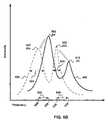
- FIG. 5Aillustrates graph of an exemplary spectrum of a beam reflected by the die, after been treated mathematically to show the frequencies related to the different layers on the die, of FIG. 4A , according to one embodiment.
- FIG. 5Billustrates the exemplary spectrum of FIG. 5A and a reference spectrum, according to one embodiment.
- FIG. 6is a flow diagram of an exemplary process tool operation method, according to one embodiment.
- FIG. 7is a flow diagram of an exemplary process tool calibration method, according to one embodiment.
- FIG. 8is a flow diagram of an exemplary process tool development method, according to one embodiment.
- FIG. 1Ais a block diagram illustrating an environment 100 for processing a substrate 106 .
- the processing environment 100includes a process tool 102 and a metrology tool 104 .
- the substrate 106may include a silicon wafer, a photolithographic mask, a gallium arsenide wafer, a germanium wafer, etc.
- the process tool 102is configured to perform a process on the substrate 106 .
- FIG. 1Aonly one process tool 102 is illustrated in FIG. 1A ; however, a person of ordinary skill in the art would understand that multiple process tools 102 may each perform one or more processes on the layer of the substrate 106 .
- a typical substratemay include one or more semiconductor devices arranged on the substrate as an array of one or more dies, while a typical semiconductor device may include multiple layers (e.g., source layer, drain layer, capacitor layer, resistor layer, gate layer, contact pad layer, conductor layer, etc.).
- Typical processesinclude deposition of material onto the substrate 106 , removal of material from the substrate 106 , patterning of the substrate 106 , and selective modification of the chemical composition of material in the substrate 106 to modify electrical properties of patterned regions.
- the electrical properties of the substrate 106may be modified by techniques such as doping selected regions on the substrate 106 using diffusion furnaces, implantation, rapid thermal anneal (RTA), exposure to ultraviolet light in UV processing (UVP), etc.
- the optical properties of the substrate 106may also be modified during modification of the electrical properties.
- Deposition of materialincludes growing, coating, or otherwise transferring a layer of material onto the substrate 106 .
- Well known deposition techniquesinclude physical vapor deposition (PVD), chemical vapor deposition (CVD), electrochemical deposition (ECD), molecular beam epitaxy (MBE), atomic layer deposition (ALD) and other methods.
- the process tool 102may be configured to selectively remove material from one or more layers of the substrate 106 , or remove the material from the substrate 106 in bulk.
- materialmay be removed using an etch process, such as wet etching in a chemical bath and/or dry etching using an ion bombardment such as reactive ion etch.
- the process tool 102may use etch processing to selectively remove exposed regions of a substrate after a photolithographic mask has been applied.
- the process tool 102my be configured to remove material in bulk using, for example, etch processing, chemical-mechanical planarization (CMP) or a chemical-mechanical polishing process to planarize a top surface of the substrate 106 between levels.
- CMPchemical-mechanical planarization
- Patterning techniquesare typically used for selectively depositing or removing material and/or controlling the shape of the deposited material.
- the substrate 106is coated with a photoresist. Selected portions of the photoresist may be exposed using a lithographic mask. The exposed regions of photoresist on the substrate 106 are then washed away by a developer solution. Alternatively, the unexposed regions of the photoresist may be washed away by the developer solution. The process tool 102 may then deposit material onto, remove material from, or modify material in the regions of the substrate 106 where the photoresist has been has been washed away.
- Deposition, removal, and/or modificationmay be performed in multiple steps on the substrate 106 . Some steps may leave a layer of material on the substrate 106 which has optical properties, such as an index of refraction, coefficient of transmission, coefficient of extinction, etc.
- the process tool 102may produce a uniform layer of material across the substrate 106 or may produce a layer in selective locations on the substrate 106 using lithographic techniques, as described elsewhere herein.
- the metrology tool 104is configured to measure a property of at least one layer of material on the substrate 106 that has been deposited, removed, and/or modified by the process tool 102 .
- the metrology tool 104is further configured to provide information about the one or more layers of the material on the substrate 106 to the process tool 102 .
- the process tool 102may use the information received from the metrology tool 104 to modify a process being applied to a subsequent substrate 106 .
- FIG. 1Bis a block diagram illustrating an alternative embodiment of an environment 100 for processing the substrate 106 .
- FIG. 1Bdiffers from FIG. 1A in that the metrology tool 104 is configured to measure the substrate 106 while the substrate 106 is in the process tool 102 and a process is being performed on the substrate 106 .
- the process tool 102is configured to receive measurements from the metrology tool 104 during the process and modify the process according to the information received from the metrology tool.
- the process tool 102may receive real time measurements of a thickness of one or more layers of the substrate 106 from the metrology tool 104 during material deposition, and may stop the deposition in response to the real time measurements to achieve a desired thickness of the one or more layers.
- FIG. 2is a block diagram illustrating the metrology tool 104 of FIG. 1A and/or 1 B, according to one embodiment.
- the metrology tool 104includes a light source 202 , an emitter/receiver 204 , an emitter/receiver array 206 , an optional spectrometer 208 , and an optional processor 210 .
- the light source 202is configured to produce a light.
- the lightmay be coupled to the emitter/receiver 202 using an optional fiber optic conductor 212 .
- the emitter/receiver 204is configured to emit an incident light beam 214 at the substrate 106 .
- the emitter/receiver 204may be combined with the light source 202 , and the fiber optic conductor 212 may be omitted.
- the light source 202may include an incandescent light, a light emitting diode (LED), a laser, etc.
- the light source 202may be configured to emit the incident light beam 214 as monochromatic light or as light in one or more selected bands of the visible, infrared, and/or ultraviolet light spectrum.
- the light beam 214may include polarized light, non-polarized light, or a combination of polarized and non-polarized light.
- the light source 202may be configured to emit a beam in the electromagnetic spectrum outside the light spectrum.
- the emitter/receiver 204may include optical components configured to collimate and/or focus the incident light beam 214 (e.g., at a plane of the substrate 106 ), using techniques which are known in the optic art.
- the light source 202may be configured to provide a continuous incident light beam 214 , pulsed incident light beam 214 , an on demand incident light beam 214 , and so forth.
- the emitter/receiver array 206is configured to dispose the emitter/receiver 204 in a position for emitting the incident light beam 214 at the substrate 106 . While only one emitter/receiver 204 is illustrated in the emitter/receiver array 206 of FIG. 2 , it is contemplated that there are a plurality of emitter/receivers 204 may be disposed in the emitter/receiver array 206 . Multiple emitter/receivers 204 disposed in the emitter/receiver array 206 may provide simultaneous measurements of multiple sites on the substrate 106 , thus enhancing throughput. In some embodiments, the emitter/receiver 204 may be configured to emit the incident light beam 214 normal to the substrate 106 , which may render the light beam 106 less sensitive to effects of an uneven surface in the substrate 106 .
- the incident light beam 214may be configured to illuminate a region 218 on the substrate 106 , and may be reflected from the substrate 106 , becoming a reflected light beam 216 .
- the emitter/receiver 204may be further configured to receive the reflected light beam 216 . While the emitter and the receiver of the emitter/receiver 204 are illustrated as combined, the emitter may be disposed in a separate location on the emitter/receiver array 206 from the receiver.
- the metrology tool 104may be configured to illuminate the substrate 106 while the substrate 106 is located inside the metrology tool 104 ; alternatively, the metrology tool 104 may be positioned near a path of the substrate 106 .
- the metrology tool 104is configured to illuminate the substrate 106 with the incident light beam 214 and receive the reflected light beam 216 while the substrate 106 is in transit on a path of the substrate 106 .
- the metrology tool 104may be combined with the process tool 102 and configured to illuminate the substrate 106 while the substrate 106 is inside the process tool 102 .
- the spectrometer 208is configured to receive the reflected light beam 216 from the emitter/receiver 204 and convert the reflected light beam 216 to a digital signal having a format of intensity as a function of wavelength.
- the processor 210is configured to receive the digital signal from the spectrometer 208 and determine a spectrum of the reflected light beam 216 from digital signal.
- the processor 210may use a Fourier transform and/or various other transforms (e.g., a chirplet transform, a Hartley transform, a Z-transform, a constant-Q transform, etc.) to determine the spectrum of the reflected light beam 216 .
- the processor 210may use hardware, firmware, and/or software to determine the spectrum.
- the processor 210may include a digital signal processor (DSP), including firmware, configured to determine the spectrum of the reflected light beam 216 .
- DSPdigital signal processor
- the processormay also receive a digital signal representing incident light beam 214 and determine the spectrum of the incident light beam 214 .
- the processor 210 and the spectrometer 208may be combined.
- the processormay be further configured to use the digital data received from the spectrometer 208 to determine a property of at least one layer of material on the substrate 106 that has been deposited, removed and/or modified by the process tool 102 .
- the spectrometer 208is combined with a spectrum analyzer configured to determine a spectrum of the reflected light beam 216 .
- the spectrum analyzermay determine the spectrum using software and/or hardware similar to the processor 210 .
- the spectrometer 208may also receive the incident light beam 214 and the spectrum analyzer may determine the spectrum of the incident light beam 214 .
- the processor 210may receive the spectrum data from the spectrum analyzer. In some embodiments the processor 210 , the spectrometer 208 , and the spectrum analyzer may be combined.
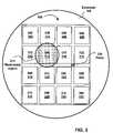
- FIG. 3is a top plan view of an exemplary substrate 106 .
- the surface of the substrate 106is illustrated as including an array of dies 300 , which includes dies 302 - 332 .
- the dies 302 - 332may be identical, different, or comprise one or more repeating patterns of sub arrays or any other arrangement.
- the region 218is illustrated as illuminating an exemplary die 312 . In various embodiments, the region 218 may illuminate the entire die 312 , a portion of the die 312 , another die of the array 300 , or multiple dies (e.g., die 314 , 316 , 322 , and 324 ).
- the substratemay be illuminated using the light beam 214 without damaging or modifying the portion of the substrate 106 in the region 218 , e.g., the die 312 .
- a proxy 334may be included on the surface of the substrate 106 (e.g., between the dies in streets and/or alleys) for monitoring the process tool 102 .
- FIG. 4Ais a perspective view of an exemplary cross-section 400 of a die such as the die 312 in the substrate 106 of FIG. 3 .
- the die 312includes layers 402 and 404 .
- the layer 404includes one or more production features F 1 , F 2 , F 3 , . . . Fn (F 1 -Fn) that may be illuminated within the region 218 .
- F 1 -Fnproduction features F 1 , F 2 , F 3 , . . . Fn (F 1 -Fn) that may be illuminated within the region 218 .
- the layer 404may include thousands or millions of production features F 1 -Fn falling within the region 218 .
- the production features F 1 -Fnmay include a plurality of features having a common property.
- the production features F 1 -Fnmay include some number of filled trenches, all placed in the layer 404 within the region 218 of the substrate 106 and having about the same thickness.
- each production feature F 1 -Fnmay have certain properties, such as thicknesses, d 1 1 , d 1 2 , d 1 3 , . . . d 1 n (d 1 1 -d 1 n ), respectively. While d 1 1 -d 1 n are used in FIG. 4A to represent thicknesses of production features F 1 -Fn respectively, a practitioner with ordinary skill in the art will understand that d 1 1 -d 1 n may also represent properties other than thickness, such as index of refraction, coefficient of absorption, etc.
- the layer 402may include a bulk layer of material disposed above the layer 404 of production features F 1 -Fn.
- the layer 402may have different properties, such as thicknesses d 2 1 , d 2 2 , d 2 3 , . . . d 2 n (d 2 1 -d 2 n ), immediately above the different production features F 1 -Fn respectively. While d 2 1 -d 2 n are used illustratively to represent thicknesses of the layer 402 above the production features F 1 -Fn respectively, a practitioner with ordinary skill in the art will again understand that d 2 1 -d 2 n may also represent properties other than thickness, such as index of refraction, coefficient of absorption, etc.
- FIG. 4Bis a perspective view of an effective die 312 ′.
- the die 312 ′represents a mathematical model of the die 312 .
- the die 312 ′includes a layer 404 ′, and a layer 402 ′.
- the die 312 ′further includes an effective feature F in the layer 404 ′, which is equivalent to combining the production features F 1 -Fn in the layer 404 into a single feature.
- the effective feature Fhas an effective thickness D 1 .
- the effective thickness D 1is mathematically equivalent to the average of the individual thicknesses d 1 1 -d 1 n of the respective production features F 1 -Fn.
- the layer 402 ′includes the bulk layer of material disposed above the layer 404 ′.
- the layer 402 ′includes an effective thickness D 2 of the bulk layer of material immediately above the effective feature F.
- the effective thickness D 2is mathematically equivalent to the average of the thicknesses d 2 1 -d 2 n of the material immediately above the respective features F 1 -Fn.
- the spectrum of the reflected light beam 216 from the cross-section 400 of the die 312is mathematically equivalent to a spectrum of a reflected light beam that would be measured from an effective cross-section 410 of the effective die 312 .
- the term virtual cross-sectionis equivalent to the term effective cross-section.
- an actual die 312 ′may be constructed.
- the proxy 334may be constructed having the effective cross-section 410 .
- a light beam reflected from the proxy 334has a spectrum representative of the cross-section 410 .
- the spectrum of the actual cross-section 400may include additional information.
- an array of dense, small features F 1 -Fnmay react differently to a process condition than an equivalent large isolated feature such as the effected feature F.
- the standard deviation of the thicknesses d 1 -dnthat may not be available from the spectrum of the effective cross-section 410 .
- FIG. 5Aillustrates a graph of an exemplary spectrum 500 of a beam reflected by the die 312 of FIG. 4A .
- the horizontal axismay represent frequency, wave length, or other parameters.
- the vertical axismay represent intensity, amplitude, photon count, or other parameters.
- the spectrum 500shows intensity versus frequency and has a peak 502 at a frequency 506 with a width 504 .
- the spectrum 500further has a lesser peak 512 at a frequency 516 with a width 514 .
- the frequency 506 of the peak 502may indicate a property such as the effective thickness D 1 of the effective feature F in the layer 404 ′ in the die 312 ′, which is equivalent to the average of the individual thicknesses of d 1 -dn of features F 1 -Fn respectively.
- the frequency 516 of the peak 512may similarly indicate the effective thickness D 2 of the material in the layer 402 ′ above the effective feature F, which is equivalent to the average of the thicknesses d 2 1 -d 2 n of the material immediately above the respective features F 1 -Fn.
- the effective cross-section 410may be represented by the frequencies 506 and 516 of the peaks 502 and 512 respectively.
- the width 504 of the peak 502may indicate a uniformity of the thicknesses d 1 1 -d 1 n of the production features F 1 -Fn in the layer 404 of the die 312 , while the width 514 of the peak 512 may likewise indicate a uniformity of the thicknesses d 2 1 -d 2 n of the material in the layer 402 above those features.
- the widths 504 and 514may also indicate the random noise in the reflected light beam 216 .
- the noise of the peaks 502 and 512generally depends on the number of features F 1 -Fn, i.e., increasing the number of features averaged into the spectrum may decrease the noise.
- height of the peak 502may indicate the number of features F 1 -Fn.
- FIG. 5Billustrates the exemplary spectrum 500 of FIG. 5A and a possible reference spectrum 520 .
- the reference spectrum 520includes a peak 522 at a frequency 526 with a width 524 and another peak 532 at a frequency 536 with a width 534 .
- the peak 522may be representative of the effective thickness D 1 r of a reference substrate.
- the peak 532may be representative of the effective thickness D 2 r of the reference substrate.
- the reference spectrum 520may be determined using optical measurements of a reference substrate which has known performance characteristics, or by averaging the measurements of a group of such substrates.
- the reference substratemay be determined using optical measurements of a proxy (e.g., the proxy 334 ).
- the thicknesses D 1 r and D 2 rmay be determined directly, for example, using SEM measurements of thicknesses of the layers of the reference substrate (or group of reference substrates) and/or the proxy 334 .
- the reference spectrum 520may also be calculated numerically and/or analytically using desired thicknesses D 1 r and D 2 r of a mathematical model of a reference substrate.
- the reference spectrum 520may be used to resolve ambiguities in associating features in the spectrum 500 determined using the metrology tool 104 with features within the substrate 106 . For example, in some cases it may be unclear whether the peak 502 or the peak 512 in the spectrum 500 is associated with the effective thickness D 2 . However, a comparison to the reference spectrum 520 might indicate that the peak 512 corresponds to the peak 532 -and can be associated with the effective thickness D 2 , while the peak 502 corresponds to the peak 522 and can be associated with the effective thickness D 1 .
- the frequency 506 of the peak 502 in the spectrum 500may be compared to the frequency 526 of the peak 522 in the reference spectrum 520 , to determine the difference 542 .
- the frequency 516 of the peak 512 in the spectrum 500might be compared to the frequency 536 of the peak 532 in the reference spectrum 520 , to determine the difference 540 .
- the frequencies 506 and 516 , the widths 504 and 514 , the frequency differences 540 and 542 , and the reference frequencies 526 and 536may be used singularly and/or in various combinations for adjusting the process tool 102 .
- Adjustments to the process tool 102may include determining process parameters, characterizing equations for determining process parameters, characterizing equations for determining properties of layers based on the frequencies, characterizing the process parameters and so forth.
- FIGS. 5A and 5Bare illustrative only, and that a spectrum 500 including more than two peaks and/or a reference spectrum 520 including more than two peaks may be used.
- the number of peaks that may be usefuli.e., the resolution of the spectrum 500 and/or the reference spectrum 520 , may be increased when the peak widths are decreased and/or the bandwidth of the incident light beam 214 is increased.
- the peak widths 504 and 514may be decreased (and the peak heights increased) by increasing the diameter of the region 218 , thus decreasing the noise by increasing the number of features F 1 -Fn averaged into the spectrum 520 .
- the spectrum 500 and reference spectrum 520may be represented as entries in an array or a database including peaks, mean frequencies, statistical distributions, vectors, raw data, etc.
- FIG. 6is flow diagram of an exemplary process tool operation method 600 , according to one embodiment.
- a substratesuch as the substrate 106 , which has been output from a process tool, such as the process tool 102 , is measured using a metrology tool, such as the metrology tool 104 .
- the measurementsare used for monitoring and providing adjustment to the process tool 102 .
- the method 600may be used to sample a small number of the substrates 106 output from the process tool 102 . Alternatively, all or most of the substrates 106 that are output from the process tool 102 may be placed in the metrology tool 104 for measurement.
- step 602the substrate 106 is placed in or near the metrology tool 104 in an appropriate location for conducting measurements, as discussed above.
- step 604the optical properties of the substrate 106 are measured using the metrology tool 104 .
- measuring the optical propertiesmay include using a spectrometer and processor, such as the spectrometer 208 and the processor 210 , to determine the spectrum 500 of the reflected light beam 216 from the substrate 106 .
- Optical propertiesinclude the spectrum 500 of the reflected light beam 216 , as well as properties inferred from the spectrum 500 , such as thickness, index of refraction, coefficient of transmission, and so forth.
- the optical propertiesmay be represented by entries in a database, including peaks, mean frequencies, statistical distributions, vectors, raw data, etc.
- step 606the optical properties of the substrate 106 are compared to reference properties, which may be determined by various methods as discussed previously.
- the reference propertiesmay also be represented by entries in a database.
- optical propertiesare assigned to layers in the substrate 106 , based on properties of the layers in the reference substrate.
- the peaks 502 and 512 in the spectrum 500may be associated with the peaks 522 and 532 in the reference spectrum 520 respectively.
- the peaks 502 and 512 in the spectrum 500may be assigned to the thicknesses D 1 and D 2 respectively.
- the comparison with the reference propertiesmay be used to resolve ambiguities in assigning the optical properties to the layers.
- an effective cross-sectionis constructed.
- the optical properties of the substrate 106may be used to calculate the effective cross-section of the substrate 106 .
- the relationship between frequency 506 of the peak 502 and frequency 526 of the peak 522may be used to determine the effective thickness D 1 of the die 312 in substrate 106 .
- Equations 1 and 2illustrate a relationship between the effective thickness D 1 and the frequency 506 , and between effective thickness D 2 and the frequency 516 respectively, as simple linear equations.
- the relationships illustrated by Equations 1 and/or 2could be represented by polynomials of arbitrary degree, logarithmic expressions, exponential expressions, sinusoidal expressions, differential equations, integral expressions, or other equations.
- the effective cross-sectionis compared to the desired cross-section.
- the effective cross-sectionmay be represented by the spectrum 500 and may be compared to a desired spectrum, such as the reference spectrum 520 .
- the effective cross-sectionmay be represented by the cross-section calculated in step 610 , for example, the thicknesses D 1 and D 2 .
- the desired thicknessmay be represented by the reference thicknesses D 1r and D 2r , which are determined from the reference spectrum 520 .
- the spectrum of the desired cross-sectionmay not be available.
- the desired cross-sectionmay be represented by thicknesses of features in a cross-section for which no spectrum has been measured or calculated.
- the desired thicknessesmay have been defined at the design stage, determined theoretically from physical models, or measured microscopically.
- the thicknesses D 1 and D 2are compared to values which represent desired thicknesses.
- step 614it is determined whether the effective cross-section is acceptable. In some embodiments, it may be determined whether the effective cross-section is acceptable without calculating or constructing the effective cross-section from the spectrum. For example, the determination may be made by comparing spectrum 500 of the substrate to the reference spectrum 520 . In such determination, the frequencies 506 and 516 in the spectrum 500 may be compared to the reference frequencies 526 and, 536 respectively in the reference spectrum 520 . Alternatively, the effective cross-section may be determined to be acceptable when the difference 542 is less than a predetermined value and/or the difference 540 is less than a predetermined value. If the effective cross-section is determined to be acceptable at step 614 then the method 600 ends. In another example, the effective cross-section may be determined to be acceptable after a predetermined number of tries. If the effective cross-section is determined to not be acceptable at step 614 then the method 600 continues to step 616
- step 616the optical properties (e.g., the frequencies 506 and 516 , the widths 504 and 514 , etc.) and the relationships between the observed spectrum and the reference spectrum (e.g., Equations 1 and 2) are reported to the process tool 102 .
- the optical propertiese.g., the frequencies 506 and 516 , the widths 504 and 514 , etc.
- the relationships between the observed spectrum and the reference spectrume.g., Equations 1 and 2
- process parametersare calculated for the process tool 102 based on the comparison of the optical properties of the substrate 106 to the reference properties (e.g., the frequencies 506 and 516 , the widths 504 and 514 , etc.).
- process parametersmay include time, concentrations of chemicals, flux of ions, field strength of magnetic and/or electric fields, angular velocity of a spinning substrate, distance between a substrate and a source, etc.
- the process tool 102may use the new process parameters to continue production in the production environment 100 .
- the process parameter T 1may be determined using a process relationship represented by a linear equation including optical properties of multiple layers.
- Equation 3 and Equation 4are linear equations. However, a practitioner with ordinary skill in the art would recognize that the process relationships illustrated by Equations 3 and/or 4 may be represented by polynomials of arbitrary degree, logarithmic expressions, exponential expressions, sinusoidal expressions, differential equations, integral expressions, etc.
- the method 600returns to step 602 where subsequent substrates in the processing environment 100 may be placed in the metrology tool 104 for measuring and providing further instructions for the process tool 102 .
- FIG. 7is a flow diagram of exemplary process tool calibration method 700 , according to one embodiment.
- the steps 702 - 712 of the method 700may be identical to the steps 602 - 612 respectively of the method 600 .
- the measurements made in the steps 702 - 712may be used for calculating adjustments for the process tool 102 , as discussed elsewhere herein.
- a databaseis constructed of effective cross-sections and process parameters.
- the process parameters used by the process tool 102 to produce substrates 106may be associated with the effective cross-sections for the respective substrates 106 in the database.
- the databasemay contain data from prior substrates having desirable characteristics and/or from mathematical models of the substrates, and/or may contain data from proxies.
- the database entriesmay include peaks, mean frequencies, statistical distributions, vectors, etc.
- step 716it is determined whether the effective cross-section is acceptable, i.e., whether the effective cross-section matches the reference cross-section. If the effective cross-section is acceptable then the process relationships (e.g., Equations 3 and/or 4) may be sufficiently accurate to use during production for correcting the process parameters in the process tool 102 , and method 700 may end. If the effective cross-section is not acceptable, the method 700 proceeds to step 718 .
- step 718process relationships are calculated based on the data in the database.
- the proportionality constant Hi and/or base exposure time constant C 1 in Equation 3may be calculated in step 718 using the database of effective cross-sections and associated process parameters.
- the constants H 1 and/or C 1may be calculated using numerical analysis, graphical methods, statistical analysis, statistical curve fitting, etc.
- the constants H 1 , H 2 , and/or C 1may be calculated for Equation 4 in step 718 by applying numerical analysis, graphical methods, statistical analysis, statistical curve fitting, etc to the database of effective cross-sections and associated process parameters.
- step 720new process parameters are calculated using the optical parameters as inputs to the new process relationships calculated in step 718 .
- the thicknesses D 1 , D 2 , D 1 r , and D 2 rmay be input to Equation 3 and/or 4 and the process parameters T 1 and/or T 2 may be determined using the new values for H 1 , H 2 , and/or C 1 , calculated in step 718 .
- the optical parametersmay be represented by the thicknesses D 1 , D 2 , D 1 r , and D 2 r
- the thicknesses D 1 , D 2 , D 1 r , and D 2 rmay be derived from direct optical measurements (e.g., frequencies f 1 , f 1r , f 2 , f 2r , etc.) using Equation 1 and 2.
- the optical parametersmay be represented by the frequencies f 1 , f 1r , f 2 , f 2r which may be used as inputs to the Equation 3 and/or 4 for calculating process parameters T 1 and/or T 2 respectively.
- the method 700Upon calculating the process parameters at step 720 , the method 700 returns to step 702 where subsequent substrates in the production environment 100 may be placed in the metrology tool 104 for measuring and for providing further data for the database in step 714 .
- FIG. 8is a flow diagram of an exemplary process tool development method 800 , according to one embodiment.
- the steps 802 - 814 of the method 800may be identical to the steps 602 - 614 respectively of the method 600 .
- the measurements made in the steps 802 - 814may be used for calculating optical properties for the substrate 106 and/or process adjustments for the process tool 102 .
- step 816the optical properties (e.g., the thickness D 2 and/or D 1 ) are compared with respective physical properties of the substrate 106 (e.g., the direct measurements of an actual cross-section 400 from light microscopy, SEM, and so forth), cross-section
- step 818the optical relationship between the optical properties of the substrate and the desired optical properties are calculated using the comparison of step 816 .
- the comparison of step 816may be used to calculate constants (e.g., K 1 , K 2 , etc.) for the relationships of Equation 1, Equation 2, and any other equations of interest.
- the comparison of step 816is used in step 818 to calculate constants (e.g., H 1 , H 2 , and/or C 1 ) for process relationships represented by Equation 3 and/or Equation 4.
- the accuracy of the constantssuch as K 1 , K 2 , H 1 , H 2 , C 1 , etc., may be improved using historical data from measurements of previous substrates 106 .
- the process parametersare calculated using the comparisons of step 816 and the process relationships.
- the method 800Upon calculating the optical properties, the process parameters, and/or process relationships at step 818 , the method 800 returns to step 802 where subsequent substrates in the production environment 100 may be placed in the metrology tool 104 for measuring and for providing further data for comparison at step 816 and refining constants at step 818 .
- the emitted light beammay be emitted at a moving substrate (e.g., translation and/or rotation).
- the emitter/receiver arraymay be configured for translation and/or rotation with respect to the substrate.
- the emitter/receivermay emit the light beam and/or receive the reflected light via fiber optics.
- the reflected light beammay be received from a moving substrate.
- Various embodiments of the inventioninclude logic stored on computer readable media, the logic configured to perform methods of the invention.
Landscapes
- Physics & Mathematics (AREA)
- General Physics & Mathematics (AREA)
- Length Measuring Devices By Optical Means (AREA)
Abstract
Description
The present application incorporates by reference U.S. Provisional Patent Application Ser. No. 60/816,815 filed on Jun. 26, 2006 for “Integrating a Metrology Instrument for Multi-film Testing,” U.S. Provisional Patent Application Ser. No. 60/817,014 filed on Jun. 26, 2006 for “Thickness and Optical Property of a Multi-film Stack Using Wavelength Illumination Filtering for Film Separation,” and U.S. Provisional Patent Application Ser. No. 60/816,893 filed on Jun. 26, 2006 for “System and Methods for Single Wafer Process Control.”
1. Field of the Invention
The present invention relates to semi-conductor manufacturing equipment and more particularly a method and apparatus for providing instructions to process tools.
2. Description of Related Art
Semiconductor manufacturing involves various steps such as adding material to a layer, removing material from a layer or modifying a layer of a substrate. Material may be added, removed, and/or modified selectively or in bulk. The steps may result in modifying physical properties of the layers, such as thickness of the layer, index of refraction of the layer, coefficient of absorption of the layer etc., which may affect the performance of the semiconductor. Thus, it is useful to measure and control the properties of the various layers.
One method of measuring the properties is to cut (e.g., scribe and break) the substrate through a feature of interest, thus exposing a cross-section of the feature. The feature may then be examined using microscopy, for example, scanning electron microscopy (SEM). Unfortunately, the substrate is generally destroyed by cutting. Moreover, the number of features that can be examined may be limited to features lying along the cut.
Another method includes creating a proxy in the form of features that are intended to be representative of one or more dies. The proxies may be placed between selected dies on the substrate. The features in the proxy may be measured during various steps in the manufacturing process using a probe in the form of a light beam having small spot size about the size of the proxy structure. However, it can be difficult to align the substrate and position the proxies within such a small spot size. Unfortunately, features in the proxies may not be representative of features in the dies.
Other methods of measuring properties of layers of a substrate include using SEM review and/or metrology tools that do not involve destroying the substrate. However, the SEM beam may burn areas of the substrate, and alignment of the small SEM beam may be difficult and/or time consuming. What is needed is an improved apparatus and method for measuring properties of a substrate to allow instructions to be sent to the process tools during operations or for future operations.
One embodiment of the present invention describes a method for providing instructions to a process tool. The method comprises emitting an incident light beam at a substrate, receiving a reflected light beam from the substrate, and determining a spectrum of the reflected light beam. The spectrum of the reflected light beam is used to determine a first property of a first layer of the substrate and a second property of a second layer of the substrate. The first property is compared to a first reference property and the second property is compared a second reference property. The first property comparison and second property comparison are used in determining the instructions which are provided to the process tool.
In various embodiments, the first and/or second properties include layer thickness, index of refraction, coefficient of absorption, and/or the like. In some embodiments, the substrate may be a wafer. In some embodiments, the process tool may use the instructions for processing subsequent substrates. Optionally, the process tool may respond to the instructions in real time while the substrate is in the process tool.
In another embodiment, the method further comprises determining properties of the first and second layers of a second substrate. The properties of the second substrate may be used with the properties of the first substrate to calibrate the process tool.
Another alternative embodiment further comprises using a spectrum from a reference wafer in determining the first and second reference properties. Alternatively, the first and second reference properties are determined from a database of spectra from two or more substrates. In some embodiments, the first and second reference properties are calculated using mathematical models.
For example, the electrical properties of thesubstrate 106 may be modified by techniques such as doping selected regions on thesubstrate 106 using diffusion furnaces, implantation, rapid thermal anneal (RTA), exposure to ultraviolet light in UV processing (UVP), etc. In some embodiments, the optical properties of thesubstrate 106 may also be modified during modification of the electrical properties.
Deposition of material includes growing, coating, or otherwise transferring a layer of material onto thesubstrate 106. Well known deposition techniques include physical vapor deposition (PVD), chemical vapor deposition (CVD), electrochemical deposition (ECD), molecular beam epitaxy (MBE), atomic layer deposition (ALD) and other methods.
In various embodiments, theprocess tool 102 may be configured to selectively remove material from one or more layers of thesubstrate 106, or remove the material from thesubstrate 106 in bulk. For example, material may be removed using an etch process, such as wet etching in a chemical bath and/or dry etching using an ion bombardment such as reactive ion etch. In some embodiments, theprocess tool 102 may use etch processing to selectively remove exposed regions of a substrate after a photolithographic mask has been applied. Alternatively, theprocess tool 102 my be configured to remove material in bulk using, for example, etch processing, chemical-mechanical planarization (CMP) or a chemical-mechanical polishing process to planarize a top surface of thesubstrate 106 between levels.
Patterning techniques are typically used for selectively depositing or removing material and/or controlling the shape of the deposited material. For example, in a conventional technique known as lithography, thesubstrate 106 is coated with a photoresist. Selected portions of the photoresist may be exposed using a lithographic mask. The exposed regions of photoresist on thesubstrate 106 are then washed away by a developer solution. Alternatively, the unexposed regions of the photoresist may be washed away by the developer solution. Theprocess tool 102 may then deposit material onto, remove material from, or modify material in the regions of thesubstrate 106 where the photoresist has been has been washed away.
Deposition, removal, and/or modification may be performed in multiple steps on thesubstrate 106. Some steps may leave a layer of material on thesubstrate 106 which has optical properties, such as an index of refraction, coefficient of transmission, coefficient of extinction, etc. Theprocess tool 102 may produce a uniform layer of material across thesubstrate 106 or may produce a layer in selective locations on thesubstrate 106 using lithographic techniques, as described elsewhere herein.
Themetrology tool 104 is configured to measure a property of at least one layer of material on thesubstrate 106 that has been deposited, removed, and/or modified by theprocess tool 102. Themetrology tool 104 is further configured to provide information about the one or more layers of the material on thesubstrate 106 to theprocess tool 102. Theprocess tool 102 may use the information received from themetrology tool 104 to modify a process being applied to asubsequent substrate 106.
The light source202 may be configured to emit theincident light beam 214 as monochromatic light or as light in one or more selected bands of the visible, infrared, and/or ultraviolet light spectrum. Thelight beam 214 may include polarized light, non-polarized light, or a combination of polarized and non-polarized light. In some embodiments, the light source202 may be configured to emit a beam in the electromagnetic spectrum outside the light spectrum. The emitter/receiver 204 may include optical components configured to collimate and/or focus the incident light beam214 (e.g., at a plane of the substrate106), using techniques which are known in the optic art. In various embodiments, the light source202 may be configured to provide a continuous incidentlight beam 214, pulsedincident light beam 214, an on demandincident light beam 214, and so forth.
The emitter/receiver array 206 is configured to dispose the emitter/receiver 204 in a position for emitting theincident light beam 214 at thesubstrate 106. While only one emitter/receiver 204 is illustrated in the emitter/receiver array 206 ofFIG. 2 , it is contemplated that there are a plurality of emitter/receivers 204 may be disposed in the emitter/receiver array 206. Multiple emitter/receivers 204 disposed in the emitter/receiver array 206 may provide simultaneous measurements of multiple sites on thesubstrate 106, thus enhancing throughput. In some embodiments, the emitter/receiver 204 may be configured to emit theincident light beam 214 normal to thesubstrate 106, which may render thelight beam 106 less sensitive to effects of an uneven surface in thesubstrate 106.
Theincident light beam 214 may be configured to illuminate aregion 218 on thesubstrate 106, and may be reflected from thesubstrate 106, becoming a reflectedlight beam 216. The emitter/receiver 204 may be further configured to receive the reflectedlight beam 216. While the emitter and the receiver of the emitter/receiver 204 are illustrated as combined, the emitter may be disposed in a separate location on the emitter/receiver array 206 from the receiver.
Themetrology tool 104 may be configured to illuminate thesubstrate 106 while thesubstrate 106 is located inside themetrology tool 104; alternatively, themetrology tool 104 may be positioned near a path of thesubstrate 106. Optionally, themetrology tool 104 is configured to illuminate thesubstrate 106 with theincident light beam 214 and receive the reflectedlight beam 216 while thesubstrate 106 is in transit on a path of thesubstrate 106. In some embodiments, themetrology tool 104 may be combined with theprocess tool 102 and configured to illuminate thesubstrate 106 while thesubstrate 106 is inside theprocess tool 102.
Thespectrometer 208 is configured to receive the reflectedlight beam 216 from the emitter/receiver 204 and convert the reflectedlight beam 216 to a digital signal having a format of intensity as a function of wavelength.
Theprocessor 210 is configured to receive the digital signal from thespectrometer 208 and determine a spectrum of the reflectedlight beam 216 from digital signal. Theprocessor 210 may use a Fourier transform and/or various other transforms (e.g., a chirplet transform, a Hartley transform, a Z-transform, a constant-Q transform, etc.) to determine the spectrum of the reflectedlight beam 216. In various embodiments, theprocessor 210 may use hardware, firmware, and/or software to determine the spectrum. For example, theprocessor 210 may include a digital signal processor (DSP), including firmware, configured to determine the spectrum of the reflectedlight beam 216. In some embodiments, the processor may also receive a digital signal representingincident light beam 214 and determine the spectrum of theincident light beam 214. In some embodiments theprocessor 210 and thespectrometer 208 may be combined. The processor may be further configured to use the digital data received from thespectrometer 208 to determine a property of at least one layer of material on thesubstrate 106 that has been deposited, removed and/or modified by theprocess tool 102.
Alternatively, thespectrometer 208 is combined with a spectrum analyzer configured to determine a spectrum of the reflectedlight beam 216. The spectrum analyzer may determine the spectrum using software and/or hardware similar to theprocessor 210. In some embodiments, thespectrometer 208 may also receive theincident light beam 214 and the spectrum analyzer may determine the spectrum of theincident light beam 214. Theprocessor 210 may receive the spectrum data from the spectrum analyzer. In some embodiments theprocessor 210, thespectrometer 208, and the spectrum analyzer may be combined.
Thelayer 402 may include a bulk layer of material disposed above thelayer 404 of production features F1-Fn. Thelayer 402 may have different properties, such as thicknesses d21, d22, d23, . . . d2n(d21-d2n), immediately above the different production features F1-Fn respectively. While d21-d2nare used illustratively to represent thicknesses of thelayer 402 above the production features F1-Fn respectively, a practitioner with ordinary skill in the art will again understand that d21-d2nmay also represent properties other than thickness, such as index of refraction, coefficient of absorption, etc.
Thelayer 402′ includes the bulk layer of material disposed above thelayer 404′. Thelayer 402′ includes an effective thickness D2 of the bulk layer of material immediately above the effective feature F. The effective thickness D2 is mathematically equivalent to the average of the thicknesses d21-d2nof the material immediately above the respective features F1-Fn. The spectrum of the reflectedlight beam 216 from thecross-section 400 of thedie 312 is mathematically equivalent to a spectrum of a reflected light beam that would be measured from aneffective cross-section 410 of theeffective die 312. For purposes of this application, the term virtual cross-section is equivalent to the term effective cross-section.
In some embodiments, anactual die 312′ may be constructed. For example, theproxy 334 may be constructed having theeffective cross-section 410. Thus, a light beam reflected from theproxy 334 has a spectrum representative of thecross-section 410. However, the spectrum of theactual cross-section 400 may include additional information. For example, an array of dense, small features F1-Fn, may react differently to a process condition than an equivalent large isolated feature such as the effected feature F. Moreover, the standard deviation of the thicknesses d1-dn, that may not be available from the spectrum of theeffective cross-section 410.
Thefrequency 506 of thepeak 502 may indicate a property such as the effective thickness D1 of the effective feature F in thelayer 404′ in thedie 312′, which is equivalent to the average of the individual thicknesses of d1-dn of features F1-Fn respectively. Thefrequency 516 of thepeak 512 may similarly indicate the effective thickness D2 of the material in thelayer 402′ above the effective feature F, which is equivalent to the average of the thicknesses d21-d2nof the material immediately above the respective features F1-Fn. Thus, theeffective cross-section 410 may be represented by thefrequencies peaks
Thewidth 504 of thepeak 502 may indicate a uniformity of the thicknesses d11-d1nof the production features F1-Fn in thelayer 404 of thedie 312, while thewidth 514 of thepeak 512 may likewise indicate a uniformity of the thicknesses d21-d2nof the material in thelayer 402 above those features. Thewidths light beam 216. The noise of thepeaks peak 502 may indicate the number of features F1-Fn.
Thereference spectrum 520 may be determined using optical measurements of a reference substrate which has known performance characteristics, or by averaging the measurements of a group of such substrates. Alternatively, the reference substrate may be determined using optical measurements of a proxy (e.g., the proxy334). The thicknesses D1rand D2rmay be determined directly, for example, using SEM measurements of thicknesses of the layers of the reference substrate (or group of reference substrates) and/or theproxy 334. Thereference spectrum 520 may also be calculated numerically and/or analytically using desired thicknesses D1rand D2rof a mathematical model of a reference substrate.
Thereference spectrum 520 may be used to resolve ambiguities in associating features in thespectrum 500 determined using themetrology tool 104 with features within thesubstrate 106. For example, in some cases it may be unclear whether thepeak 502 or thepeak 512 in thespectrum 500 is associated with the effective thickness D2. However, a comparison to thereference spectrum 520 might indicate that thepeak 512 corresponds to the peak532-and can be associated with the effective thickness D2, while thepeak 502 corresponds to thepeak 522 and can be associated with the effective thickness D1.
In addition, thefrequency 506 of the peak502 in thespectrum 500 may be compared to thefrequency 526 of the peak522 in thereference spectrum 520, to determine thedifference 542. Similarly, thefrequency 516 of the peak512 in thespectrum 500 might be compared to thefrequency 536 of the peak532 in thereference spectrum 520, to determine thedifference 540.
In various embodiments, thefrequencies widths frequency differences reference frequencies process tool 102. Adjustments to theprocess tool 102 may include determining process parameters, characterizing equations for determining process parameters, characterizing equations for determining properties of layers based on the frequencies, characterizing the process parameters and so forth.
It may be appreciated by a person with ordinary skill in the art thatFIGS. 5A and 5B are illustrative only, and that aspectrum 500 including more than two peaks and/or areference spectrum 520 including more than two peaks may be used. In some embodiments, the number of peaks that may be useful, i.e., the resolution of thespectrum 500 and/or thereference spectrum 520, may be increased when the peak widths are decreased and/or the bandwidth of theincident light beam 214 is increased. For example, thepeak widths region 218, thus decreasing the noise by increasing the number of features F1-Fn averaged into thespectrum 520. It may be further appreciated by a person with ordinary skill in the art that thespectrum 500 andreference spectrum 520 may be represented as entries in an array or a database including peaks, mean frequencies, statistical distributions, vectors, raw data, etc.
Instep 602 thesubstrate 106 is placed in or near themetrology tool 104 in an appropriate location for conducting measurements, as discussed above.
Instep 604 the optical properties of thesubstrate 106 are measured using themetrology tool 104. As above, measuring the optical properties may include using a spectrometer and processor, such as thespectrometer 208 and theprocessor 210, to determine thespectrum 500 of the reflectedlight beam 216 from thesubstrate 106. Optical properties include thespectrum 500 of the reflectedlight beam 216, as well as properties inferred from thespectrum 500, such as thickness, index of refraction, coefficient of transmission, and so forth. Again, the optical properties may be represented by entries in a database, including peaks, mean frequencies, statistical distributions, vectors, raw data, etc.
Instep 606 the optical properties of thesubstrate 106 are compared to reference properties, which may be determined by various methods as discussed previously. The reference properties may also be represented by entries in a database.
Inoptional step 608 optical properties are assigned to layers in thesubstrate 106, based on properties of the layers in the reference substrate. For example, as above, thepeaks spectrum 500 may be associated with thepeaks reference spectrum 520 respectively. Thus, thepeaks spectrum 500 may be assigned to the thicknesses D1 and D2 respectively. The comparison with the reference properties may be used to resolve ambiguities in assigning the optical properties to the layers.
Inoptional step 610 an effective cross-section is constructed. The optical properties of thesubstrate 106 may be used to calculate the effective cross-section of thesubstrate 106. In some embodiments, the relationship betweenfrequency 506 of thepeak 502 andfrequency 526 of thepeak 522 may be used to determine the effective thickness D1 of the die312 insubstrate 106. The effective thickness D1 may be determined from the optical equation:
D1=K1(f1−f1r)+D1r Equation 1
where K1is a proportionality constant, f1is thefrequency 506 of thepeak 502, f1ris thefrequency 526 of thepeak 522, and D1ris the thickness of the reference layer assigned to thepeak 522.
D1=K1(f1−f1r)+D1r Equation 1
where K1is a proportionality constant, f1is the
Likewise, the effective thickness D2 may be determined from the equation:
D2=K2(f2−f2r)+D2r Equation 2
where K2is a proportionality constant, f2is thefrequency 516 of thepeak 512, f2ris thefrequency 536 of thepeak 532, and D2ris the thickness of the reference layer assigned to thepeak 532.
D2=K2(f2−f2r)+D2r Equation 2
where K2is a proportionality constant, f2is the
Inoptional step 612, the effective cross-section is compared to the desired cross-section. The effective cross-section may be represented by thespectrum 500 and may be compared to a desired spectrum, such as thereference spectrum 520. Alternatively, the effective cross-section may be represented by the cross-section calculated instep 610, for example, the thicknesses D1 and D2. The desired thickness may be represented by the reference thicknesses D1rand D2r, which are determined from thereference spectrum 520.
In some cases the spectrum of the desired cross-section may not be available. In such cases, the desired cross-section may be represented by thicknesses of features in a cross-section for which no spectrum has been measured or calculated. For example, the desired thicknesses may have been defined at the design stage, determined theoretically from physical models, or measured microscopically. In such cases, the thicknesses D1 and D2 are compared to values which represent desired thicknesses.
Instep 614 it is determined whether the effective cross-section is acceptable. In some embodiments, it may be determined whether the effective cross-section is acceptable without calculating or constructing the effective cross-section from the spectrum. For example, the determination may be made by comparingspectrum 500 of the substrate to thereference spectrum 520. In such determination, thefrequencies spectrum 500 may be compared to thereference frequencies reference spectrum 520. Alternatively, the effective cross-section may be determined to be acceptable when thedifference 542 is less than a predetermined value and/or thedifference 540 is less than a predetermined value. If the effective cross-section is determined to be acceptable atstep 614 then themethod 600 ends. In another example, the effective cross-section may be determined to be acceptable after a predetermined number of tries. If the effective cross-section is determined to not be acceptable atstep 614 then themethod 600 continues to step616
Instep 616 the optical properties (e.g., thefrequencies widths process tool 102.
Instep 618 process parameters are calculated for theprocess tool 102 based on the comparison of the optical properties of thesubstrate 106 to the reference properties (e.g., thefrequencies widths
For example, a process parameter comprising a deposition time T1may be determined using a process relationship represented by the equation
T1=H1(D1−D1r)+C1 Equation 3
where H1is a proportionality constant, D1 is the effective thickness of an effective layer (e.g., thelayer 404′), D1ris the effective thickness of a reference layer, and the constant C1is a base deposition time constant. Theprocess tool 102 may use the new process parameters to continue production in theproduction environment 100.
T1=H1(D1−D1r)+C1 Equation 3
where H1is a proportionality constant, D1 is the effective thickness of an effective layer (e.g., the
In some embodiments, the process parameter T1may be determined using a process relationship represented by a linear equation including optical properties of multiple layers. For example, the process parameter T1may be determined using a process relationship represented by the equation
T1=H1(D1−D1r)+H2(D2−D2r)+C1 Equation 4
where H2is a proportionality constant, D2 is the effective thickness of another layer (e.g., thelayer 402′) and D2ris the effective thickness of another reference layer.
T1=H1(D1−D1r)+H2(D2−D2r)+C1 Equation 4
where H2is a proportionality constant, D2 is the effective thickness of another layer (e.g., the
The process relationships set forth in the examples ofEquation 3 and Equation 4 are linear equations. However, a practitioner with ordinary skill in the art would recognize that the process relationships illustrated byEquations 3 and/or 4 may be represented by polynomials of arbitrary degree, logarithmic expressions, exponential expressions, sinusoidal expressions, differential equations, integral expressions, etc.
Once the process parameters are calculated, themethod 600 returns to step602 where subsequent substrates in theprocessing environment 100 may be placed in themetrology tool 104 for measuring and providing further instructions for theprocess tool 102.
In step714 a database is constructed of effective cross-sections and process parameters. The process parameters used by theprocess tool 102 to producesubstrates 106 may be associated with the effective cross-sections for therespective substrates 106 in the database. The database may contain data from prior substrates having desirable characteristics and/or from mathematical models of the substrates, and/or may contain data from proxies. The database entries may include peaks, mean frequencies, statistical distributions, vectors, etc.
Instep 716 it is determined whether the effective cross-section is acceptable, i.e., whether the effective cross-section matches the reference cross-section. If the effective cross-section is acceptable then the process relationships (e.g.,Equations 3 and/or 4) may be sufficiently accurate to use during production for correcting the process parameters in theprocess tool 102, andmethod 700 may end. If the effective cross-section is not acceptable, themethod 700 proceeds to step718.
Instep 718 process relationships are calculated based on the data in the database. For example, the proportionality constant Hi and/or base exposure time constant C1inEquation 3 may be calculated instep 718 using the database of effective cross-sections and associated process parameters. In various embodiments, the constants H1and/or C1may be calculated using numerical analysis, graphical methods, statistical analysis, statistical curve fitting, etc.
Alternatively, the constants H1, H2, and/or C1may be calculated for Equation 4 instep 718 by applying numerical analysis, graphical methods, statistical analysis, statistical curve fitting, etc to the database of effective cross-sections and associated process parameters.
Instep 720 new process parameters are calculated using the optical parameters as inputs to the new process relationships calculated instep 718. For example, the thicknesses D1, D2, D1r, and D2r, may be input toEquation 3 and/or 4 and the process parameters T1and/or T2may be determined using the new values for H1, H2, and/or C1, calculated instep 718.
While the optical parameters may be represented by the thicknesses D1, D2, D1r, and D2r, a practitioner with ordinary skill in the art would recognize that the thicknesses D1, D2, D1r, and D2rmay be derived from direct optical measurements (e.g., frequencies f1, f1r, f2, f2r, etc.) usingEquation 1 and 2. Thus, in one embodiment, the optical parameters may be represented by the frequencies f1, f1r, f2, f2rwhich may be used as inputs to theEquation 3 and/or 4 for calculating process parameters T1and/or T2respectively.
Upon calculating the process parameters atstep 720, themethod 700 returns to step702 where subsequent substrates in theproduction environment 100 may be placed in themetrology tool 104 for measuring and for providing further data for the database instep 714.
Instep 816 the optical properties (e.g., the thickness D2 and/or D1) are compared with respective physical properties of the substrate106 (e.g., the direct measurements of anactual cross-section 400 from light microscopy, SEM, and so forth), cross-section
Instep 818 the optical relationship between the optical properties of the substrate and the desired optical properties are calculated using the comparison ofstep 816. The comparison ofstep 816 may be used to calculate constants (e.g., K1, K2, etc.) for the relationships of Equation 1,Equation 2, and any other equations of interest. Optionally, the comparison ofstep 816 is used instep 818 to calculate constants (e.g., H1, H2, and/or C1) for process relationships represented byEquation 3 and/or Equation 4. In some embodiments, the accuracy of the constants such as K1, K2, H1, H2, C1, etc., may be improved using historical data from measurements ofprevious substrates 106. Furthermore, instep 818, the process parameters are calculated using the comparisons ofstep 816 and the process relationships.
Upon calculating the optical properties, the process parameters, and/or process relationships atstep 818, themethod 800 returns to step802 where subsequent substrates in theproduction environment 100 may be placed in themetrology tool 104 for measuring and for providing further data for comparison atstep 816 and refining constants atstep 818.
Although themethods methods
Several embodiments are specifically illustrated and/or described herein. However, it will be appreciated that modifications and variations are covered by the above teachings and within the scope of the appended claims without departing from the spirit and intended scope thereof. For example, the emitted light beam may be emitted at a moving substrate (e.g., translation and/or rotation). Alternatively, the emitter/receiver array may be configured for translation and/or rotation with respect to the substrate. The emitter/receiver may emit the light beam and/or receive the reflected light via fiber optics. The reflected light beam may be received from a moving substrate. Various embodiments of the invention include logic stored on computer readable media, the logic configured to perform methods of the invention.
The embodiments discussed herein are illustrative of the present invention. As these embodiments of the present invention are described with reference to illustrations, various modifications or adaptations of the methods and or specific structures described, may become apparent to a person with ordinary skill in the art. All such modifications, adaptations, or variations that rely upon the teachings of the present invention, and through which these teachings have advanced the art, are considered to be within the spirit and scope of the present invention. Hence, these descriptions and drawings should not be considered in a limiting sense, as it is understood that the present invention is in no way limited to only the embodiments illustrated.
Claims (32)
1. A method for instructing a process tool to make adjustments to a process comprising the steps of:
emitting a first incident light beam at a first substrate;
receiving a first reflected light beam from the first substrate;
determining a first spectrum of the first reflected light beam;
determining a first property of a first layer of the first substrate based at least in part on the first spectrum;
determining a second property of a second layer of the first substrate based at least in part on the first spectrum;
determining a virtual cross-section of the substrate based on the first property and the second property;
comparing the first property to a first reference property;
comparing the second property to a second reference property;
wherein comparing the first property to the first reference property and comparing the second property to the second reference property comprises comparing the virtual cross-section of the substrate to a desired cross section;
determining desired adjustments to the process to make the properties of the first and second layers more closely conform to the first and second reference properties, based at least in part on the first property comparison and the second property comparison; and
providing instructions to the process tool to make the desired adjustments.
2. The method ofclaim 1 , further comprising adjusting a process of the process tool based on the provided instructions.
3. The method ofclaim 1 , further comprising adjusting a process of the process tool based on comparing the first property and the second property to a previous first property and a previous second property.
4. The method ofclaim 1 , wherein determining the first property is also based on the first reference property.
5. The method ofclaim 1 , wherein determining the second property is also based on the second reference property.
6. The method ofclaim 1 , wherein determining the first property is also based on the first and second reference property.
7. The method ofclaim 1 , wherein the step of determining what adjustments to the process are appropriate is further based on a comparison of the first property to the second property.
8. The method ofclaim 1 , further comprising processing a second substrate.
9. The method ofclaim 8 , further comprising:
emitting a second incident light beam at the second substrate;
receiving a second reflected light beam from the second substrate;
determining a second spectrum of the second reflected light beam;
determining a property of a layer of the second substrate based on the second spectrum;
determining a relationship based on a comparison of the first property of the first substrate to the property of the second substrate;
modifying the instructions based on the relationship; and
providing the modified instructions to the process tool.
10. The method ofclaim 9 , further comprising adjusting a process of the process tool based on the provided instructions.
11. The method ofclaim 1 , further comprising:
emitting an incident light beam at a reference substrate;
receiving a reflected light beam from the reference substrate;
determining a reference spectrum of the reflected light beam from the reference substrate;
determining a first reference property of a first layer of the reference substrate based on the reference spectrum; and
determining a second reference property of a second layer of the reference substrate based on the reference spectrum.
12. The method ofclaim 1 , wherein the first property is the thickness of the first layer of the first substrate.
13. The method ofclaim 1 , wherein the first property is the index of refraction of the first layer of the first substrate.
14. The method ofclaim 1 , wherein the first property is the coefficient of extinction of the first layer of the first substrate.
15. The method ofclaim 1 , wherein the diameter of the first incident light beam is larger than 19 millimeters.
16. A computer readable medium having embodied thereon a program, the program being executable by a computing device for performing a method for providing instructions a process tool to make adjustments to a process comprising the steps of:
emitting a first incident light beam at a first substrate;
receiving a first reflected light beam from the first substrate;
determining a first spectrum of the first reflected light beam;
determining a first property of a first layer of the first substrate based on the first spectrum;
determining a second property of a second layer of the first substrate based on the first spectrum;
determining a virtual cross-section of the substrate based on the first property and the second property;
comparing the first property to a first reference property;
comparing the second property to a second reference property;
wherein comparing the first property to the first reference property and comparing the second property to the second reference property comprises comparing the virtual cross-section of the substrate to a desired cross section;
determining what adjustments to the process are appropriate to make the properties of the first and second layers more closely conform to the first and second reference properties based on the first property comparison and the second property comparison; and
providing instructions to the process tool to make the appropriate adjustments.
17. The method ofclaim 16 , further comprising adjusting a process of the process tool based on the provided instructions.
18. The method ofclaim 16 , further comprising processing a second substrate using the instructions.
19. The method ofclaim 18 , further comprising:
emitting a second incident light beam at the second substrate;
receiving a second reflected light beam from the second substrate;
determining a second spectrum of the second reflected light beam;
determining a property of a layer of the second substrate based on the second spectrum;
determining a relationship based on a comparison of the first property of the first substrate to the property of the second substrate;
modifying the instructions based on the relationship; and
providing the modified instructions to the process tool.
20. The method ofclaim 16 , further comprising:
emitting an incident light beam at a reference substrate;
receiving a reflected light beam from the reference substrate;
determining a reference spectrum of the reflected light beam from the reference substrate;
determining a first reference property of a layer of the reference substrate based on reference spectrum; and
determining a second reference property of a second layer of the reference substrate based on the reference spectrum.
21. The method ofclaim 16 , wherein the first property is the thickness of the first layer of the first substrate.
22. The method ofclaim 16 , wherein the first property is the index of refraction of the first layer of the first substrate.
23. The method ofclaim 16 , wherein the first property is the coefficient of extinction of the first layer of the first substrate.
24. The method ofclaim 18 , wherein the diameter of the first incident light beam is larger than 19 millimeters.
25. A metrology tool for instructing a process tool to make adjustments to a process comprising:
an emitter configured to emit an incident light beam at a first substrate;
a receiver configured to receive a reflected light beam from the first substrate;
a spectrometer configured to determine the spectrum of the reflected light beam; and
a processor configured to:
determine a first property of a first layer of the first substrate based on the spectrum;
determine a second property of a second layer of the first substrate based on the spectrum;
determining a virtual cross-section of the substrate based on the first property and the second property;
compare the first property to a first reference property;
compare the second property to a second reference property; and
wherein comparing the first property to the first reference property and comparing the second property to the second reference property comprises comparing the virtual cross-section of the substrate to a desired cross section;
determine what adjustments to the process are appropriate to make the properties of the first and second layers more closely conform to the first and second reference properties based on the first property comparison and the second property comparison; and
provide the instructions to the process tool to make the appropriate adjustments.
26. The metrology tool ofclaim 25 , wherein the process tool is further configured to adjust a process of the process tool based on the provided instructions.
27. The metrology tool ofclaim 25 , wherein the process tool is further configured to process a second substrate using the instructions.
28. The metrology tool ofclaim 27 , wherein the processor is further configured to:
receive a first property of a second substrate; and
modify the determined what adjustments to the process are appropriate based on a comparison of the first property of the first substrate to the first property of the second substrate.
29. The metrology tool ofclaim 25 , wherein the first property is the thickness of the first layer of the first substrate.
30. The metrology tool ofclaim 25 , wherein the first property is the index of refraction of the first layer of the first substrate.
31. The metrology tool ofclaim 25 , wherein the first property the coefficient of transmission of the first layer of the first substrate.
32. The metrology tool ofclaim 25 , wherein the diameter of the incident light beam is larger than 19 millimeters.
Priority Applications (1)
| Application Number | Priority Date | Filing Date | Title |
|---|---|---|---|
| US11/717,327US7469164B2 (en) | 2006-06-26 | 2007-03-12 | Method and apparatus for process control with in-die metrology |
Applications Claiming Priority (4)
| Application Number | Priority Date | Filing Date | Title |
|---|---|---|---|
| US81701406P | 2006-06-26 | 2006-06-26 | |
| US81681506P | 2006-06-26 | 2006-06-26 | |
| US81689306P | 2006-06-26 | 2006-06-26 | |
| US11/717,327US7469164B2 (en) | 2006-06-26 | 2007-03-12 | Method and apparatus for process control with in-die metrology |
Publications (2)
| Publication Number | Publication Date |
|---|---|
| US20070298522A1 US20070298522A1 (en) | 2007-12-27 |
| US7469164B2true US7469164B2 (en) | 2008-12-23 |
Family
ID=38874006
Family Applications (1)
| Application Number | Title | Priority Date | Filing Date |
|---|---|---|---|
| US11/717,327ActiveUS7469164B2 (en) | 2006-06-26 | 2007-03-12 | Method and apparatus for process control with in-die metrology |
Country Status (1)
| Country | Link |
|---|---|
| US (1) | US7469164B2 (en) |
Cited By (47)
| Publication number | Priority date | Publication date | Assignee | Title |
|---|---|---|---|---|
| US20110096339A1 (en)* | 2009-10-28 | 2011-04-28 | Nanometrics Incorporated | Optical Metrology On Textured Samples |
| US8404551B2 (en) | 2010-12-03 | 2013-03-26 | Suvolta, Inc. | Source/drain extension control for advanced transistors |
| US8421162B2 (en) | 2009-09-30 | 2013-04-16 | Suvolta, Inc. | Advanced transistors with punch through suppression |
| US8461875B1 (en) | 2011-02-18 | 2013-06-11 | Suvolta, Inc. | Digital circuits having improved transistors, and methods therefor |
| US8525271B2 (en) | 2011-03-03 | 2013-09-03 | Suvolta, Inc. | Semiconductor structure with improved channel stack and method for fabrication thereof |
| US8530286B2 (en) | 2010-04-12 | 2013-09-10 | Suvolta, Inc. | Low power semiconductor transistor structure and method of fabrication thereof |
| US8569156B1 (en) | 2011-05-16 | 2013-10-29 | Suvolta, Inc. | Reducing or eliminating pre-amorphization in transistor manufacture |
| US8569128B2 (en) | 2010-06-21 | 2013-10-29 | Suvolta, Inc. | Semiconductor structure and method of fabrication thereof with mixed metal types |
| US8599623B1 (en) | 2011-12-23 | 2013-12-03 | Suvolta, Inc. | Circuits and methods for measuring circuit elements in an integrated circuit device |
| US8614128B1 (en) | 2011-08-23 | 2013-12-24 | Suvolta, Inc. | CMOS structures and processes based on selective thinning |
| US8629016B1 (en) | 2011-07-26 | 2014-01-14 | Suvolta, Inc. | Multiple transistor types formed in a common epitaxial layer by differential out-diffusion from a doped underlayer |
| US8637955B1 (en) | 2012-08-31 | 2014-01-28 | Suvolta, Inc. | Semiconductor structure with reduced junction leakage and method of fabrication thereof |
| US8645878B1 (en) | 2011-08-23 | 2014-02-04 | Suvolta, Inc. | Porting a circuit design from a first semiconductor process to a second semiconductor process |
| US8713511B1 (en) | 2011-09-16 | 2014-04-29 | Suvolta, Inc. | Tools and methods for yield-aware semiconductor manufacturing process target generation |
| US8735987B1 (en) | 2011-06-06 | 2014-05-27 | Suvolta, Inc. | CMOS gate stack structures and processes |
| US8748270B1 (en) | 2011-03-30 | 2014-06-10 | Suvolta, Inc. | Process for manufacturing an improved analog transistor |
| US8748986B1 (en) | 2011-08-05 | 2014-06-10 | Suvolta, Inc. | Electronic device with controlled threshold voltage |
| US8759872B2 (en) | 2010-06-22 | 2014-06-24 | Suvolta, Inc. | Transistor with threshold voltage set notch and method of fabrication thereof |
| US8796048B1 (en) | 2011-05-11 | 2014-08-05 | Suvolta, Inc. | Monitoring and measurement of thin film layers |
| US8811068B1 (en) | 2011-05-13 | 2014-08-19 | Suvolta, Inc. | Integrated circuit devices and methods |
| US8816754B1 (en) | 2012-11-02 | 2014-08-26 | Suvolta, Inc. | Body bias circuits and methods |
| US8819603B1 (en) | 2011-12-15 | 2014-08-26 | Suvolta, Inc. | Memory circuits and methods of making and designing the same |
| US8863064B1 (en) | 2012-03-23 | 2014-10-14 | Suvolta, Inc. | SRAM cell layout structure and devices therefrom |
| US8877619B1 (en) | 2012-01-23 | 2014-11-04 | Suvolta, Inc. | Process for manufacture of integrated circuits with different channel doping transistor architectures and devices therefrom |
| US8883600B1 (en) | 2011-12-22 | 2014-11-11 | Suvolta, Inc. | Transistor having reduced junction leakage and methods of forming thereof |
| US8895327B1 (en) | 2011-12-09 | 2014-11-25 | Suvolta, Inc. | Tipless transistors, short-tip transistors, and methods and circuits therefor |
| US8970289B1 (en) | 2012-01-23 | 2015-03-03 | Suvolta, Inc. | Circuits and devices for generating bi-directional body bias voltages, and methods therefor |
| US8982362B2 (en) | 2011-10-04 | 2015-03-17 | First Solar, Inc. | System and method for measuring layer thickness and depositing semiconductor layers |
| US8995204B2 (en) | 2011-06-23 | 2015-03-31 | Suvolta, Inc. | Circuit devices and methods having adjustable transistor body bias |
| US8999861B1 (en) | 2011-05-11 | 2015-04-07 | Suvolta, Inc. | Semiconductor structure with substitutional boron and method for fabrication thereof |
| US9041126B2 (en) | 2012-09-21 | 2015-05-26 | Mie Fujitsu Semiconductor Limited | Deeply depleted MOS transistors having a screening layer and methods thereof |
| US9054219B1 (en) | 2011-08-05 | 2015-06-09 | Mie Fujitsu Semiconductor Limited | Semiconductor devices having fin structures and fabrication methods thereof |
| US9070477B1 (en) | 2012-12-12 | 2015-06-30 | Mie Fujitsu Semiconductor Limited | Bit interleaved low voltage static random access memory (SRAM) and related methods |
| US9093550B1 (en) | 2012-01-31 | 2015-07-28 | Mie Fujitsu Semiconductor Limited | Integrated circuits having a plurality of high-K metal gate FETs with various combinations of channel foundation structure and gate stack structure and methods of making same |
| US9093997B1 (en) | 2012-11-15 | 2015-07-28 | Mie Fujitsu Semiconductor Limited | Slew based process and bias monitors and related methods |
| US9112484B1 (en) | 2012-12-20 | 2015-08-18 | Mie Fujitsu Semiconductor Limited | Integrated circuit process and bias monitors and related methods |
| US9112057B1 (en) | 2012-09-18 | 2015-08-18 | Mie Fujitsu Semiconductor Limited | Semiconductor devices with dopant migration suppression and method of fabrication thereof |
| US9236466B1 (en) | 2011-10-07 | 2016-01-12 | Mie Fujitsu Semiconductor Limited | Analog circuits having improved insulated gate transistors, and methods therefor |
| US9268885B1 (en) | 2013-02-28 | 2016-02-23 | Mie Fujitsu Semiconductor Limited | Integrated circuit device methods and models with predicted device metric variations |
| US9299801B1 (en) | 2013-03-14 | 2016-03-29 | Mie Fujitsu Semiconductor Limited | Method for fabricating a transistor device with a tuned dopant profile |
| US9299698B2 (en) | 2012-06-27 | 2016-03-29 | Mie Fujitsu Semiconductor Limited | Semiconductor structure with multiple transistors having various threshold voltages |
| US9319013B2 (en) | 2014-08-19 | 2016-04-19 | Mie Fujitsu Semiconductor Limited | Operational amplifier input offset correction with transistor threshold voltage adjustment |
| US9406567B1 (en) | 2012-02-28 | 2016-08-02 | Mie Fujitsu Semiconductor Limited | Method for fabricating multiple transistor devices on a substrate with varying threshold voltages |
| US9431068B2 (en) | 2012-10-31 | 2016-08-30 | Mie Fujitsu Semiconductor Limited | Dynamic random access memory (DRAM) with low variation transistor peripheral circuits |
| US9478571B1 (en) | 2013-05-24 | 2016-10-25 | Mie Fujitsu Semiconductor Limited | Buried channel deeply depleted channel transistor |
| US9710006B2 (en) | 2014-07-25 | 2017-07-18 | Mie Fujitsu Semiconductor Limited | Power up body bias circuits and methods |
| US10074568B2 (en) | 2009-09-30 | 2018-09-11 | Mie Fujitsu Semiconductor Limited | Electronic devices and systems, and methods for making and using same |
Families Citing this family (3)
| Publication number | Priority date | Publication date | Assignee | Title |
|---|---|---|---|---|
| TWI577523B (en)* | 2011-06-17 | 2017-04-11 | 三菱麗陽股份有限公司 | Mold having an uneven structure on its surface, optical article, and manufacturing method thereof, transparent base material for surface light emitter, and surface light emitter |
| JP7038621B2 (en)* | 2018-07-20 | 2022-03-18 | 東京エレクトロン株式会社 | Position measuring device and position measuring method |
| JP7741003B2 (en)* | 2022-01-31 | 2025-09-17 | 株式会社ディスコ | Measurement method and measurement device |
Citations (13)
| Publication number | Priority date | Publication date | Assignee | Title |
|---|---|---|---|---|
| US5867276A (en) | 1997-03-07 | 1999-02-02 | Bio-Rad Laboratories, Inc. | Method for broad wavelength scatterometry |
| US6242739B1 (en) | 1998-04-21 | 2001-06-05 | Alexander P. Cherkassky | Method and apparatus for non-destructive determination of film thickness and dopant concentration using fourier transform infrared spectrometry |
| US6383824B1 (en)* | 2001-04-25 | 2002-05-07 | Advanced Micro Devices, Inc. | Method of using scatterometry measurements to control deposition processes |
| US6413867B1 (en)* | 1999-12-23 | 2002-07-02 | Applied Materials, Inc. | Film thickness control using spectral interferometry |
| US6479309B1 (en)* | 2001-05-25 | 2002-11-12 | Advanced Micro Devices, Inc. | Method and apparatus for determining process layer conformality |
| US6483580B1 (en) | 1998-03-06 | 2002-11-19 | Kla-Tencor Technologies Corporation | Spectroscopic scatterometer system |
| US20030049390A1 (en)* | 2001-06-19 | 2003-03-13 | Applied Materials, Inc. | Feedback control of plasma-enhanced chemical vapor deposition processes |
| US6678055B2 (en) | 2001-11-26 | 2004-01-13 | Tevet Process Control Technologies Ltd. | Method and apparatus for measuring stress in semiconductor wafers |
| US6762838B2 (en) | 2001-07-02 | 2004-07-13 | Tevet Process Control Technologies Ltd. | Method and apparatus for production line screening |
| US6801321B1 (en) | 1998-08-27 | 2004-10-05 | Tevet Process Control Technologies Ltd. | Method and apparatus for measuring lateral variations in thickness or refractive index of a transparent film on a substrate |
| US6885467B2 (en) | 2002-10-28 | 2005-04-26 | Tevet Process Control Technologies Ltd. | Method and apparatus for thickness decomposition of complicated layer structures |
| US6950196B2 (en) | 2000-09-20 | 2005-09-27 | Kla-Tencor Technologies Corp. | Methods and systems for determining a thickness of a structure on a specimen and at least one additional property of the specimen |
| US7092096B2 (en)* | 2004-02-20 | 2006-08-15 | Taiwan Semiconductor Manufacturing Co., Ltd. | Optical scatterometry method of sidewall spacer analysis |
- 2007
- 2007-03-12USUS11/717,327patent/US7469164B2/enactiveActive
Patent Citations (13)
| Publication number | Priority date | Publication date | Assignee | Title |
|---|---|---|---|---|
| US5867276A (en) | 1997-03-07 | 1999-02-02 | Bio-Rad Laboratories, Inc. | Method for broad wavelength scatterometry |
| US6483580B1 (en) | 1998-03-06 | 2002-11-19 | Kla-Tencor Technologies Corporation | Spectroscopic scatterometer system |
| US6242739B1 (en) | 1998-04-21 | 2001-06-05 | Alexander P. Cherkassky | Method and apparatus for non-destructive determination of film thickness and dopant concentration using fourier transform infrared spectrometry |
| US6801321B1 (en) | 1998-08-27 | 2004-10-05 | Tevet Process Control Technologies Ltd. | Method and apparatus for measuring lateral variations in thickness or refractive index of a transparent film on a substrate |
| US6413867B1 (en)* | 1999-12-23 | 2002-07-02 | Applied Materials, Inc. | Film thickness control using spectral interferometry |
| US6950196B2 (en) | 2000-09-20 | 2005-09-27 | Kla-Tencor Technologies Corp. | Methods and systems for determining a thickness of a structure on a specimen and at least one additional property of the specimen |
| US6383824B1 (en)* | 2001-04-25 | 2002-05-07 | Advanced Micro Devices, Inc. | Method of using scatterometry measurements to control deposition processes |
| US6479309B1 (en)* | 2001-05-25 | 2002-11-12 | Advanced Micro Devices, Inc. | Method and apparatus for determining process layer conformality |
| US20030049390A1 (en)* | 2001-06-19 | 2003-03-13 | Applied Materials, Inc. | Feedback control of plasma-enhanced chemical vapor deposition processes |
| US6762838B2 (en) | 2001-07-02 | 2004-07-13 | Tevet Process Control Technologies Ltd. | Method and apparatus for production line screening |
| US6678055B2 (en) | 2001-11-26 | 2004-01-13 | Tevet Process Control Technologies Ltd. | Method and apparatus for measuring stress in semiconductor wafers |
| US6885467B2 (en) | 2002-10-28 | 2005-04-26 | Tevet Process Control Technologies Ltd. | Method and apparatus for thickness decomposition of complicated layer structures |
| US7092096B2 (en)* | 2004-02-20 | 2006-08-15 | Taiwan Semiconductor Manufacturing Co., Ltd. | Optical scatterometry method of sidewall spacer analysis |
Non-Patent Citations (1)
| Title |
|---|
| Ying Wang, "Integrated dielectric trench-depth measurement for dual damascene", Solid State Technology, vol. 42, No. 12, Dec. 1, 2004, 8 pgs total. |
Cited By (98)
| Publication number | Priority date | Publication date | Assignee | Title |
|---|---|---|---|---|
| US9508800B2 (en) | 2009-09-30 | 2016-11-29 | Mie Fujitsu Semiconductor Limited | Advanced transistors with punch through suppression |
| US11887895B2 (en) | 2009-09-30 | 2024-01-30 | United Semiconductor Japan Co., Ltd. | Electronic devices and systems, and methods for making and using the same |
| US9263523B2 (en) | 2009-09-30 | 2016-02-16 | Mie Fujitsu Semiconductor Limited | Advanced transistors with punch through suppression |
| US10074568B2 (en) | 2009-09-30 | 2018-09-11 | Mie Fujitsu Semiconductor Limited | Electronic devices and systems, and methods for making and using same |
| US8421162B2 (en) | 2009-09-30 | 2013-04-16 | Suvolta, Inc. | Advanced transistors with punch through suppression |
| US10217668B2 (en) | 2009-09-30 | 2019-02-26 | Mie Fujitsu Semiconductor Limited | Electronic devices and systems, and methods for making and using the same |
| US10224244B2 (en) | 2009-09-30 | 2019-03-05 | Mie Fujitsu Semiconductor Limited | Electronic devices and systems, and methods for making and using the same |
| US10325986B2 (en) | 2009-09-30 | 2019-06-18 | Mie Fujitsu Semiconductor Limited | Advanced transistors with punch through suppression |
| US11062950B2 (en) | 2009-09-30 | 2021-07-13 | United Semiconductor Japan Co., Ltd. | Electronic devices and systems, and methods for making and using the same |
| WO2011053484A1 (en)* | 2009-10-28 | 2011-05-05 | Nanometrics Incorporated | Optical metrology on textured samples |
| US8379227B2 (en)* | 2009-10-28 | 2013-02-19 | Nanometrics Incorporated | Optical metrology on textured samples |
| US20110096339A1 (en)* | 2009-10-28 | 2011-04-28 | Nanometrics Incorporated | Optical Metrology On Textured Samples |
| US9865596B2 (en) | 2010-04-12 | 2018-01-09 | Mie Fujitsu Semiconductor Limited | Low power semiconductor transistor structure and method of fabrication thereof |
| US8530286B2 (en) | 2010-04-12 | 2013-09-10 | Suvolta, Inc. | Low power semiconductor transistor structure and method of fabrication thereof |
| US9496261B2 (en) | 2010-04-12 | 2016-11-15 | Mie Fujitsu Semiconductor Limited | Low power semiconductor transistor structure and method of fabrication thereof |
| US9224733B2 (en) | 2010-06-21 | 2015-12-29 | Mie Fujitsu Semiconductor Limited | Semiconductor structure and method of fabrication thereof with mixed metal types |
| US8569128B2 (en) | 2010-06-21 | 2013-10-29 | Suvolta, Inc. | Semiconductor structure and method of fabrication thereof with mixed metal types |
| US9418987B2 (en) | 2010-06-22 | 2016-08-16 | Mie Fujitsu Semiconductor Limited | Transistor with threshold voltage set notch and method of fabrication thereof |
| US8759872B2 (en) | 2010-06-22 | 2014-06-24 | Suvolta, Inc. | Transistor with threshold voltage set notch and method of fabrication thereof |
| US9922977B2 (en) | 2010-06-22 | 2018-03-20 | Mie Fujitsu Semiconductor Limited | Transistor with threshold voltage set notch and method of fabrication thereof |
| US8686511B2 (en) | 2010-12-03 | 2014-04-01 | Suvolta, Inc. | Source/drain extension control for advanced transistors |
| US8563384B2 (en) | 2010-12-03 | 2013-10-22 | Suvolta, Inc. | Source/drain extension control for advanced transistors |
| US8404551B2 (en) | 2010-12-03 | 2013-03-26 | Suvolta, Inc. | Source/drain extension control for advanced transistors |
| US9006843B2 (en) | 2010-12-03 | 2015-04-14 | Suvolta, Inc. | Source/drain extension control for advanced transistors |
| US10250257B2 (en) | 2011-02-18 | 2019-04-02 | Mie Fujitsu Semiconductor Limited | Digital circuits having improved transistors, and methods therefor |
| US8461875B1 (en) | 2011-02-18 | 2013-06-11 | Suvolta, Inc. | Digital circuits having improved transistors, and methods therefor |
| US9680470B2 (en) | 2011-02-18 | 2017-06-13 | Mie Fujitsu Semiconductor Limited | Digital circuits having improved transistors, and methods therefor |
| US9985631B2 (en) | 2011-02-18 | 2018-05-29 | Mie Fujitsu Semiconductor Limited | Digital circuits having improved transistors, and methods therefor |
| US9838012B2 (en) | 2011-02-18 | 2017-12-05 | Mie Fujitsu Semiconductor Limited | Digital circuits having improved transistors, and methods therefor |
| US9184750B1 (en) | 2011-02-18 | 2015-11-10 | Mie Fujitsu Semiconductor Limited | Digital circuits having improved transistors, and methods therefor |
| US8525271B2 (en) | 2011-03-03 | 2013-09-03 | Suvolta, Inc. | Semiconductor structure with improved channel stack and method for fabrication thereof |
| US9111785B2 (en) | 2011-03-03 | 2015-08-18 | Mie Fujitsu Semiconductor Limited | Semiconductor structure with improved channel stack and method for fabrication thereof |
| US8748270B1 (en) | 2011-03-30 | 2014-06-10 | Suvolta, Inc. | Process for manufacturing an improved analog transistor |
| US9093469B2 (en) | 2011-03-30 | 2015-07-28 | Mie Fujitsu Semiconductor Limited | Analog transistor |
| US8999861B1 (en) | 2011-05-11 | 2015-04-07 | Suvolta, Inc. | Semiconductor structure with substitutional boron and method for fabrication thereof |
| US8796048B1 (en) | 2011-05-11 | 2014-08-05 | Suvolta, Inc. | Monitoring and measurement of thin film layers |
| US8811068B1 (en) | 2011-05-13 | 2014-08-19 | Suvolta, Inc. | Integrated circuit devices and methods |
| US9741428B2 (en) | 2011-05-13 | 2017-08-22 | Mie Fujitsu Semiconductor Limited | Integrated circuit devices and methods |
| US9966130B2 (en) | 2011-05-13 | 2018-05-08 | Mie Fujitsu Semiconductor Limited | Integrated circuit devices and methods |
| US9362291B1 (en) | 2011-05-13 | 2016-06-07 | Mie Fujitsu Semiconductor Limited | Integrated circuit devices and methods |
| US8569156B1 (en) | 2011-05-16 | 2013-10-29 | Suvolta, Inc. | Reducing or eliminating pre-amorphization in transistor manufacture |
| US9793172B2 (en) | 2011-05-16 | 2017-10-17 | Mie Fujitsu Semiconductor Limited | Reducing or eliminating pre-amorphization in transistor manufacture |
| US8937005B2 (en) | 2011-05-16 | 2015-01-20 | Suvolta, Inc. | Reducing or eliminating pre-amorphization in transistor manufacture |
| US9514940B2 (en) | 2011-05-16 | 2016-12-06 | Mie Fujitsu Semiconductor Limited | Reducing or eliminating pre-amorphization in transistor manufacture |
| US9281248B1 (en) | 2011-06-06 | 2016-03-08 | Mie Fujitsu Semiconductor Limited | CMOS gate stack structures and processes |
| US8735987B1 (en) | 2011-06-06 | 2014-05-27 | Suvolta, Inc. | CMOS gate stack structures and processes |
| US8995204B2 (en) | 2011-06-23 | 2015-03-31 | Suvolta, Inc. | Circuit devices and methods having adjustable transistor body bias |
| US8629016B1 (en) | 2011-07-26 | 2014-01-14 | Suvolta, Inc. | Multiple transistor types formed in a common epitaxial layer by differential out-diffusion from a doped underlayer |
| US8653604B1 (en) | 2011-07-26 | 2014-02-18 | Suvolta, Inc. | Multiple transistor types formed in a common epitaxial layer by differential out-diffusion from a doped underlayer |
| US8916937B1 (en) | 2011-07-26 | 2014-12-23 | Suvolta, Inc. | Multiple transistor types formed in a common epitaxial layer by differential out-diffusion from a doped underlayer |
| US9054219B1 (en) | 2011-08-05 | 2015-06-09 | Mie Fujitsu Semiconductor Limited | Semiconductor devices having fin structures and fabrication methods thereof |
| US8748986B1 (en) | 2011-08-05 | 2014-06-10 | Suvolta, Inc. | Electronic device with controlled threshold voltage |
| US8963249B1 (en) | 2011-08-05 | 2015-02-24 | Suvolta, Inc. | Electronic device with controlled threshold voltage |
| US8645878B1 (en) | 2011-08-23 | 2014-02-04 | Suvolta, Inc. | Porting a circuit design from a first semiconductor process to a second semiconductor process |
| US8806395B1 (en) | 2011-08-23 | 2014-08-12 | Suvolta, Inc. | Porting a circuit design from a first semiconductor process to a second semiconductor process |
| US9117746B1 (en) | 2011-08-23 | 2015-08-25 | Mie Fujitsu Semiconductor Limited | Porting a circuit design from a first semiconductor process to a second semiconductor process |
| US8614128B1 (en) | 2011-08-23 | 2013-12-24 | Suvolta, Inc. | CMOS structures and processes based on selective thinning |
| US9391076B1 (en) | 2011-08-23 | 2016-07-12 | Mie Fujitsu Semiconductor Limited | CMOS structures and processes based on selective thinning |
| US8713511B1 (en) | 2011-09-16 | 2014-04-29 | Suvolta, Inc. | Tools and methods for yield-aware semiconductor manufacturing process target generation |
| US8982362B2 (en) | 2011-10-04 | 2015-03-17 | First Solar, Inc. | System and method for measuring layer thickness and depositing semiconductor layers |
| US9236466B1 (en) | 2011-10-07 | 2016-01-12 | Mie Fujitsu Semiconductor Limited | Analog circuits having improved insulated gate transistors, and methods therefor |
| US8895327B1 (en) | 2011-12-09 | 2014-11-25 | Suvolta, Inc. | Tipless transistors, short-tip transistors, and methods and circuits therefor |
| US8819603B1 (en) | 2011-12-15 | 2014-08-26 | Suvolta, Inc. | Memory circuits and methods of making and designing the same |
| US9196727B2 (en) | 2011-12-22 | 2015-11-24 | Mie Fujitsu Semiconductor Limited | High uniformity screen and epitaxial layers for CMOS devices |
| US9368624B2 (en) | 2011-12-22 | 2016-06-14 | Mie Fujitsu Semiconductor Limited | Method for fabricating a transistor with reduced junction leakage current |
| US8883600B1 (en) | 2011-12-22 | 2014-11-11 | Suvolta, Inc. | Transistor having reduced junction leakage and methods of forming thereof |
| US8599623B1 (en) | 2011-12-23 | 2013-12-03 | Suvolta, Inc. | Circuits and methods for measuring circuit elements in an integrated circuit device |
| US8970289B1 (en) | 2012-01-23 | 2015-03-03 | Suvolta, Inc. | Circuits and devices for generating bi-directional body bias voltages, and methods therefor |
| US8877619B1 (en) | 2012-01-23 | 2014-11-04 | Suvolta, Inc. | Process for manufacture of integrated circuits with different channel doping transistor architectures and devices therefrom |
| US9093550B1 (en) | 2012-01-31 | 2015-07-28 | Mie Fujitsu Semiconductor Limited | Integrated circuits having a plurality of high-K metal gate FETs with various combinations of channel foundation structure and gate stack structure and methods of making same |
| US9385047B2 (en) | 2012-01-31 | 2016-07-05 | Mie Fujitsu Semiconductor Limited | Integrated circuits having a plurality of high-K metal gate FETs with various combinations of channel foundation structure and gate stack structure and methods of making same |
| US9406567B1 (en) | 2012-02-28 | 2016-08-02 | Mie Fujitsu Semiconductor Limited | Method for fabricating multiple transistor devices on a substrate with varying threshold voltages |
| US8863064B1 (en) | 2012-03-23 | 2014-10-14 | Suvolta, Inc. | SRAM cell layout structure and devices therefrom |
| US9299698B2 (en) | 2012-06-27 | 2016-03-29 | Mie Fujitsu Semiconductor Limited | Semiconductor structure with multiple transistors having various threshold voltages |
| US9812550B2 (en) | 2012-06-27 | 2017-11-07 | Mie Fujitsu Semiconductor Limited | Semiconductor structure with multiple transistors having various threshold voltages |
| US10217838B2 (en) | 2012-06-27 | 2019-02-26 | Mie Fujitsu Semiconductor Limited | Semiconductor structure with multiple transistors having various threshold voltages |
| US10014387B2 (en) | 2012-06-27 | 2018-07-03 | Mie Fujitsu Semiconductor Limited | Semiconductor structure with multiple transistors having various threshold voltages |
| US9105711B2 (en) | 2012-08-31 | 2015-08-11 | Mie Fujitsu Semiconductor Limited | Semiconductor structure with reduced junction leakage and method of fabrication thereof |
| US8637955B1 (en) | 2012-08-31 | 2014-01-28 | Suvolta, Inc. | Semiconductor structure with reduced junction leakage and method of fabrication thereof |
| US9112057B1 (en) | 2012-09-18 | 2015-08-18 | Mie Fujitsu Semiconductor Limited | Semiconductor devices with dopant migration suppression and method of fabrication thereof |
| US9041126B2 (en) | 2012-09-21 | 2015-05-26 | Mie Fujitsu Semiconductor Limited | Deeply depleted MOS transistors having a screening layer and methods thereof |
| US9431068B2 (en) | 2012-10-31 | 2016-08-30 | Mie Fujitsu Semiconductor Limited | Dynamic random access memory (DRAM) with low variation transistor peripheral circuits |
| US9154123B1 (en) | 2012-11-02 | 2015-10-06 | Mie Fujitsu Semiconductor Limited | Body bias circuits and methods |
| US8816754B1 (en) | 2012-11-02 | 2014-08-26 | Suvolta, Inc. | Body bias circuits and methods |
| US9319034B2 (en) | 2012-11-15 | 2016-04-19 | Mie Fujitsu Semiconductor Limited | Slew based process and bias monitors and related methods |
| US9093997B1 (en) | 2012-11-15 | 2015-07-28 | Mie Fujitsu Semiconductor Limited | Slew based process and bias monitors and related methods |
| US9070477B1 (en) | 2012-12-12 | 2015-06-30 | Mie Fujitsu Semiconductor Limited | Bit interleaved low voltage static random access memory (SRAM) and related methods |
| US9276561B2 (en) | 2012-12-20 | 2016-03-01 | Mie Fujitsu Semiconductor Limited | Integrated circuit process and bias monitors and related methods |
| US9112484B1 (en) | 2012-12-20 | 2015-08-18 | Mie Fujitsu Semiconductor Limited | Integrated circuit process and bias monitors and related methods |
| US9268885B1 (en) | 2013-02-28 | 2016-02-23 | Mie Fujitsu Semiconductor Limited | Integrated circuit device methods and models with predicted device metric variations |
| US9893148B2 (en) | 2013-03-14 | 2018-02-13 | Mie Fujitsu Semiconductor Limited | Method for fabricating a transistor device with a tuned dopant profile |
| US9577041B2 (en) | 2013-03-14 | 2017-02-21 | Mie Fujitsu Semiconductor Limited | Method for fabricating a transistor device with a tuned dopant profile |
| US9299801B1 (en) | 2013-03-14 | 2016-03-29 | Mie Fujitsu Semiconductor Limited | Method for fabricating a transistor device with a tuned dopant profile |
| US9991300B2 (en) | 2013-05-24 | 2018-06-05 | Mie Fujitsu Semiconductor Limited | Buried channel deeply depleted channel transistor |
| US9786703B2 (en) | 2013-05-24 | 2017-10-10 | Mie Fujitsu Semiconductor Limited | Buried channel deeply depleted channel transistor |
| US9478571B1 (en) | 2013-05-24 | 2016-10-25 | Mie Fujitsu Semiconductor Limited | Buried channel deeply depleted channel transistor |
| US9710006B2 (en) | 2014-07-25 | 2017-07-18 | Mie Fujitsu Semiconductor Limited | Power up body bias circuits and methods |
| US9319013B2 (en) | 2014-08-19 | 2016-04-19 | Mie Fujitsu Semiconductor Limited | Operational amplifier input offset correction with transistor threshold voltage adjustment |
Also Published As
| Publication number | Publication date |
|---|---|
| US20070298522A1 (en) | 2007-12-27 |
Similar Documents
| Publication | Publication Date | Title |
|---|---|---|
| US7469164B2 (en) | Method and apparatus for process control with in-die metrology | |
| KR100942039B1 (en) | How to Measure Features with Asymmetric Profiles | |
| JP5102329B2 (en) | Measurement of diffractive structures, broadband, polarization, ellipsometry and underlying structures | |
| US10490462B2 (en) | Metrology systems and methods for process control | |
| US7023549B2 (en) | Parametric profiling using optical spectroscopic systems | |
| US7280230B2 (en) | Parametric profiling using optical spectroscopic systems | |
| JP5444610B2 (en) | Method for measuring process parameters of semiconductor manufacturing process using optical measurement | |
| KR102220435B1 (en) | Measurement model optimization based on parameter variations across a wafer | |
| TWI303090B (en) | Method for in-situ monitoring of patterned substrate processing using reflectometry | |
| US7085676B2 (en) | Feed forward critical dimension control | |
| TW201643405A (en) | Optical metrology with reduced focus error sensitivity | |
| KR20040091157A (en) | Metrology diffraction signal adaptation for tool-to-tool matching | |
| KR100625168B1 (en) | Inspection method for the pattern formed on the substrate and inspection apparatus for performing the same | |
| US7492467B1 (en) | Method and apparatus for measuring thickness and optical properties of a thin-film on a substrate | |
| US20250105064A1 (en) | Electrical Performance Prediction Based On Structural Measurements Of Partially Fabricated Semiconductor Devices | |
| JP2000091210A (en) | Exposure apparatus, exposure amount function setting method and exposure method |
Legal Events
| Date | Code | Title | Description |
|---|---|---|---|
| AS | Assignment | Owner name:TEVET PCT LTD., ISRAEL Free format text:ASSIGNMENT OF ASSIGNORS INTEREST;ASSIGNOR:DU-NOUR, OFER;REEL/FRAME:019089/0482 Effective date:20070311 | |
| AS | Assignment | Owner name:NANOMETRICS INCORPORATED, CALIFORNIA Free format text:ASSIGNMENT OF ASSIGNORS INTEREST;ASSIGNOR:TEVET PROCESS CONTROL TECHNOLOGIES, LTD.;REEL/FRAME:021194/0642 Effective date:20080703 | |
| STCF | Information on status: patent grant | Free format text:PATENTED CASE | |
| FPAY | Fee payment | Year of fee payment:4 | |
| FPAY | Fee payment | Year of fee payment:8 | |
| AS | Assignment | Owner name:ONTO INNOVATION INC., MASSACHUSETTS Free format text:CHANGE OF NAME;ASSIGNOR:NANOMETRICS INCORPORATED;REEL/FRAME:052544/0224 Effective date:20191025 | |
| MAFP | Maintenance fee payment | Free format text:PAYMENT OF MAINTENANCE FEE, 12TH YEAR, LARGE ENTITY (ORIGINAL EVENT CODE: M1553); ENTITY STATUS OF PATENT OWNER: LARGE ENTITY Year of fee payment:12 |