US7468686B2 - Systems and methods for providing compact digitally controlled trim of multi-segment circuits - Google Patents
Systems and methods for providing compact digitally controlled trim of multi-segment circuitsDownload PDFInfo
- Publication number
- US7468686B2 US7468686B2US11/671,666US67166607AUS7468686B2US 7468686 B2US7468686 B2US 7468686B2US 67166607 AUS67166607 AUS 67166607AUS 7468686 B2US7468686 B2US 7468686B2
- Authority
- US
- United States
- Prior art keywords
- dac
- circuit
- electronic circuit
- adjusting
- range
- Prior art date
- Legal status (The legal status is an assumption and is not a legal conclusion. Google has not performed a legal analysis and makes no representation as to the accuracy of the status listed.)
- Active, expires
Links
- 238000000034methodMethods0.000titleclaimsdescription26
- 230000000694effectsEffects0.000claimsdescription26
- 230000006870functionEffects0.000claimsdescription6
- 238000012546transferMethods0.000claimsdescription6
- 229920005994diacetyl cellulosePolymers0.000description13
- 238000010586diagramMethods0.000description10
- 230000005540biological transmissionEffects0.000description7
- 230000035945sensitivityEffects0.000description4
- 230000000295complement effectEffects0.000description3
- 238000009966trimmingMethods0.000description2
- 230000003213activating effectEffects0.000description1
- 238000013459approachMethods0.000description1
- 230000008901benefitEffects0.000description1
- 238000007664blowingMethods0.000description1
- 238000012937correctionMethods0.000description1
- 230000001934delayEffects0.000description1
- 238000013461designMethods0.000description1
- 238000009826distributionMethods0.000description1
- 230000003993interactionEffects0.000description1
- 238000005259measurementMethods0.000description1
- 238000012986modificationMethods0.000description1
- 230000004048modificationEffects0.000description1
- 238000009828non-uniform distributionMethods0.000description1
- 230000008569processEffects0.000description1
- 238000011084recoveryMethods0.000description1
- 230000007704transitionEffects0.000description1
Images


Classifications
- H—ELECTRICITY
- H03—ELECTRONIC CIRCUITRY
- H03M—CODING; DECODING; CODE CONVERSION IN GENERAL
- H03M1/00—Analogue/digital conversion; Digital/analogue conversion
- H03M1/10—Calibration or testing
- H03M1/1009—Calibration
- H03M1/1033—Calibration over the full range of the converter, e.g. for correcting differential non-linearity
- H03M1/1057—Calibration over the full range of the converter, e.g. for correcting differential non-linearity by trimming, i.e. by individually adjusting at least part of the quantisation value generators or stages to their nominal values
- H03M1/1061—Calibration over the full range of the converter, e.g. for correcting differential non-linearity by trimming, i.e. by individually adjusting at least part of the quantisation value generators or stages to their nominal values using digitally programmable trimming circuits
- H—ELECTRICITY
- H03—ELECTRONIC CIRCUITRY
- H03M—CODING; DECODING; CODE CONVERSION IN GENERAL
- H03M1/00—Analogue/digital conversion; Digital/analogue conversion
- H03M1/66—Digital/analogue converters
- H03M1/68—Digital/analogue converters with conversions of different sensitivity, i.e. one conversion relating to the more significant digital bits and another conversion to the less significant bits
- H03M1/687—Segmented, i.e. the more significant bit converter being of the unary decoded type and the less significant bit converter being of the binary weighted type
- H—ELECTRICITY
- H03—ELECTRONIC CIRCUITRY
- H03M—CODING; DECODING; CODE CONVERSION IN GENERAL
- H03M1/00—Analogue/digital conversion; Digital/analogue conversion
- H03M1/66—Digital/analogue converters
- H03M1/74—Simultaneous conversion
- H03M1/76—Simultaneous conversion using switching tree
- H03M1/765—Simultaneous conversion using switching tree using a single level of switches which are controlled by unary decoded digital signals
- H—ELECTRICITY
- H03—ELECTRONIC CIRCUITRY
- H03M—CODING; DECODING; CODE CONVERSION IN GENERAL
- H03M1/00—Analogue/digital conversion; Digital/analogue conversion
- H03M1/66—Digital/analogue converters
- H03M1/74—Simultaneous conversion
- H03M1/78—Simultaneous conversion using ladder network
- H03M1/785—Simultaneous conversion using ladder network using resistors, i.e. R-2R ladders
- H—ELECTRICITY
- H03—ELECTRONIC CIRCUITRY
- H03M—CODING; DECODING; CODE CONVERSION IN GENERAL
- H03M1/00—Analogue/digital conversion; Digital/analogue conversion
- H03M1/66—Digital/analogue converters
- H03M1/74—Simultaneous conversion
- H03M1/80—Simultaneous conversion using weighted impedances
- H03M1/808—Simultaneous conversion using weighted impedances using resistors
Definitions
- the present inventionrelates to providing a practical, compact digitally-controlled trim of a circuit having a digital input, such as a Digital-to-Analog Converter (DAC). More particularly, this invention relates to applying the trim to more than one element or location in the circuit. Often, these types of circuits include elements or trim locations that have a strong effect on the output for some input code states, and a very weak effect, for other code states.
- DACDigital-to-Analog Converter
- DACstranslate binary signals from computers or other discrete circuitry into proportional analog voltage levels, DACs are commonly used to drive analog devices such as meters, motor controllers, or audio circuitry.
- the binary weighted resistor network DACis the simplest method of converting digital bits from a digital signal into an analog signal.
- a binary signalis applied to gating circuits 118 that drive analog switches 102 , 104 , 106 and 108 .
- a binary signal of 0000is applied to the switches, all the switches are open so no voltage is applied to the op amp 122 , At this point, the output is 0 volts.
- switch 102closes and 10 volts is applied to resistor 110 .
- op amp 122represents virtual ground, there is 10 volts across the 8000 ohm resistor 110 , That causes 10 V/8000 ohm, or 1.25 milliamps, to flow through the 800 ohm feedback resistor 120 .
- the voltage across resistor 120would be 800 ohm ⁇ 1.25 milliamps, or 1 volt.
- switch 102opens and switch 104 closes. That causes 2.5 milliamps (10 volts/4000 ohms) to flow through resistor 120 . The voltage across resistor 120 is then 800 ohms ⁇ 2.5 milliamps, or 2 volts. A binary 0100 would create 4 volts at the output, and so on,
- a binary-weighted resistor network DACis not practical, however, for applications requiring much more than 4 bits of resolution because the range of resistor values required is very large and difficult to fabricate accurately.
- An R 2R ladder networkhas become the DAG of choice, therefore, in most applications.
- the R 2R ladder networkis capable of producing binary weighted voltages with resistors having only two different values of resistance arranged in a type of network known as a binary ladder, shown in FIG. 2 .
- a series of latches 240are used to drive analog switches 202 , 204 , 206 and 208 .
- the R-2R ladderoperates such that, when an individual switch is closed, each “rung” on the R-2R ladder delivers a current to the virtual ground node. Because of the arrangement of resistors 210 , 212 , 214 , 216 , 218 , 220 , 222 and 224 , the current delivered by each successive rung is binarily weighted. Thus, each successive switch going down the ladder, when connected, produces a current, which, in turn, produces half the output voltage of the switch above it.
- the primary advantage of the binary ladder design over the binary weighted resistor network DACis its use of resistors having only two resistor values. As a result, it is a simple matter to process virtually any number of bits simply by adding additional “rungs” to the ladder.
- resistor ladder DACsoperating in the voltage switching (VOUT) mode, different bits have different propagation delay through the resistor ladder to the output. These different propagation delays typically create large major carry glitch impulse errors, A major carry occurs when an MSB (most significant bit) is turned OFF and all the LSBs (lease significant bits) are turned ON.
- thermometer codedAs opposed to binary-encoded because a four-bit thermometer code has fifteen distinct transitions representing the sixteen possible values of a four-bit input, i.e., from 0000 to 1111. These bits do not require resistors between successive segments because they provide sequentially weighted signals and not binarily weighted signals. Any number of the bits in the DAC can be thermometer-encoded.
- thermometer-coded bitsAnother reason to segment the MSBs into one group of thermometer-coded bits is to reduce the sensitivity of the transfer function to any one ladder element.
- a 16-bit DACmay have its four MSBs broken down into (15) equivalent MSB segments, each having a weight of 4,096 LSBs.
- Such DACsgenerally use laser trim—i.e., using a laser to adjust the resistances of the resistors in the DAC to implement the addition or subtraction of a small voltage to obtain a more linear result (a result that more closely corresponds to the ideal analog output of the converter) from the output of the DAC.
- a continuous trim resistor trim tabi.e., wherein a portion of a resistor of pre-determined configuration or shape is selectively shaped using a Laser—is typically used.
- Some prior art DACsalso use “link trims” in which a resistive element or elements in a complicated resistor network is selectively entirely opened by the laser to obtain a total resistance that corresponds to the optimal resistance of the segment of the DAC.
- a problem with continuous tab trimsis that they are typically slow. A new, precise measurement of error must be made after each small increment of the laser position in order to determine when to stop the trim—i.e., when to terminate the laser burn of the resistor. Another problem is that resistor tab trims are prone to post trim drift. These problems are further compounded by a high number of MSB segments,
- Link trimsare generally faster and less prone to post trim drift, but they consume far more area, since many bits of link trim—i.e., resistors in a complex resistor network—may be needed to achieve the required trim range and resolution. The area penalty becomes much greater when more than a few bits of trim are used because additional elements are needed to achieve the wide range in trim weights.
- the inventionincludes a circuit for adjusting the output of a DAC by adjusting a plurality of resistor segments in the DAC.
- the circuitpreferably includes a programmable Read Only Memory (ROM).
- ROMRead Only Memory
- the ROMmay include a plurality of multi-bit digital words. Each of the digital words may control a plurality of variable impedance structures. Each of the plurality of variable impedance structures may be configured to adjust a resistor segment in the DAC.
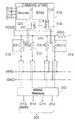
- FIG. 1is a schematic diagram of a conventional binary-weighted resistor network DAC
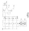
- FIG. 2is a schematic diagram of a conventional segmented ladder network DAC
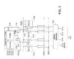
- FIG. 3is a schematic diagram of a portion of an R-2R ladder network DAC according to the invention.
- FIG. 4is a diagram that shows the effect on DAC linearity of full-scale trim at a number of selected trim locations
- FIG. 5is a diagram that shows the effect of one embodiment of full-scale trim according to the invention.
- FIG. 6is a schematic diagram that illustrates a portion of FIG. 5 in greater detail
- FIG. 7is a diagram that shows a portion of FIG. 6 in greater detail.
- FIG. 8is a diagram that shows a portion of FIG. 7 in greater detail
- the proposed circuits and methodsuse a fully link based trim, which preferably substantially eliminates the trim time and post-trim drift problems of tab trims.
- the fine trim of the MSB segmentsis preferably performed by programming a ROM containing fourteen (14) 8-bit words. Accordingly, the ROM controls a compact 8-bit trimdac structure. Although the trimdac is more complicated and larger than the trim link structure required to trim a single segment, it is far smaller than the (15) such trim structures that would be required to trim all segments.
- the ROM wordis preferably selected based on the state of (4) DAC MSB's, D 15 , D 14 , D 13 and D 12 .
- S 0 and S 15all of the (15) MSB segments are all tied low or high, respectfully, which may make the trimdac according to the invention ineffective.
- trimdac based trimto the segmented MSBs of a voltage switching resistor ladder DAC Because the circuit is passive and has extremely small full scale and zero scale errors, the trim must be applied by adjusting one or more of the existing resistor segments. However, the sensitivity of Vout to a variation in any single resistor segment is higher in some regions of the DAC transfer function and very low in others.
- FIG. 3shows a simplified block diagram for a circuit according to the invention
- FIG. 3shows how the trimdac 316 ties into the RS 1 and RS 15 segments 312 and 314 (only RS 1 , RS 2 , RS 14 and RS 15 of the (15) SDAC segments are shown)
- Trimdac 316includes ROM 318 and decode 320
- Trimdac 316is also configured to receive inputs from the four MSBs 305 (bits D 12 -D 15 ) in order to identify the state of the MSBs.
- the respective states of the MSBsprovide the information necessary to determine which ROM word stored in trimdac 306 to select.
- trimdac 316may preferably be implemented for a different complementary pair of the segments of the MSBs—e.g., for pair RS 1 312 and RS 15 314 (as shown), for pair RS 2 313 and RS 14 315 (as shown), for pair RS 3 and RS 14 (not shown), etc.
- Trimdac 316also may include variable resistors 317 and 319 (which may preferably be implemented to adjust the resistance of the resistors that they are trimming) which are set by a signal from ROM 318 ,
- Variable resistors 317 and 313which may be implemented in any suitable fashion or impedance type, are used to correct the non-linearities of the output of the DAC.
- FIG. 4shows the effect on the DAC linearity of coarse-adjusting (trimming) the value of RSB shown in FIG. 3 ( FIG. 4A ), RS 1 ( FIG. 4B ), RS 8 ( FIG. 4C ), or RS 15 (FIG, 4 D), respectively.
- trimdac 316finely trims/adjusts both RS 1 and RS 15 preferably substantially simultaneously, but in a complementary fashion—e.g., RS 15 314 is trimmed to have higher resistance when RS 1 312 is trimmed to have lower resistance and vice versa.
- variable resistance circuits 317 and 319which are controlled by a single 8-bit ROM word.
- the circuits 317 and 319preferably receive 2's complement-coded inputs, so midscale corresponds to no trim and +/ ⁇ Full Scale correspond to ⁇ 3.8 LSB and +3.8 LSB of INL trim, respectively.
- FIG. 5shows the possible fine trim adjustments achievable with the trimdac 316 .
- the upper and lower envelopes 502 and 504 of the graphsshow the INL trim produced if the trimdac code is held at +FS (full scale) or ⁇ FS.
- the 14 regions in between 506represent the range of DAC codes where trimdac 316 may be controlled by each of the (14) ROM words, and the individual lines 508 in each of the regions 506 shown represent an arbitrary set of possible ROM codes.
- 8-bit trimdac 316(which could be configured with any suitable number of bits) is divided into (2) MSB, (3) Middle Bits, and (3) LSB sections. Each of these different sections preferably tie into (are preferably implemented with) different tap points in the RS 1 /RS 15 resistor structure. This serves to minimize bit interaction, which may be difficult to avoid in variable resistor circuits.
- controlled Rsw transmission switch structuresmay be controlled by the input (ROM) code to set the trimdac resistance value.
- ROMinput
- Such Rsw transmission switch structuresare disclosed in copending U.S. patent application Ser. No. 11/671628 entitled, “SYSTEMS AND METHODS FOR SWITCH RESISTANCE CONTROL IN DIGITAL TO ANALOG CONVERTERS (DACS)” which is hereby incorporated by reference herein in its entirety.
- the transmission switch structuresmay have a parallel Nchannel and Pchannel pair. To turn the switch ON, the gates of the switches can be tied to VGN and VGP. In one embodiment, the transmission switch structures tie to the SW_ 1 S and SW_ 15 S nodes, which are driven to either REFHI or REFLO depending on the S 1 and S 15 digital inputs.
- the Nchannel switchhas a negative VGS and may be OFF
- the Pchannel switchhas a positive VGS and is OFF.
- FIGS. 6-8show circuits that further illustrate the use of invention with respect to transmission switch structures.
- FIG. 6shows a more detailed view of resistor 312 and resistor 317 .
- Resistor 312is preferably controlled by digital control from ROM 318 .
- FIG, 7shows a more detailed view of one implementation of resistor 317 .
- digital controlmay be input to switches 317 A-D.
- FIG. 8shows a detailed schematic diagram of an exemplary circuit 846 that may be used to implement one or all of switches 317 A-D in FIG. 7 .
- Circuit 846preferably includes a control signal 848 and buffer 850 .
- Buffer 850may be coupled to Vcc (the supply voltage) and to ground.
- Control signal 848preferably controls the operation of P-channel driver 852 and N-channel driver 854 .
- VGPthe high reference gate voltage
- VGNthe low reference gate voltage
- circuit 846is a detailed schematic of one embodiment of a circuit that may be used to implement one, some or all of switches 317 A-D shown in FIG. 7 .
- Tapped resistor string circuitsas are used in Resistor string DACs or in interpolating DACs as shown in commonly-assigned U.S. Pat. No. 6,937,178which is hereby incorporated by reference herein in its entirety show a very similar behavior of sensitivity of transfer function to individual resistor elements to the voltage switching resistor ladder case shown above. Therefore, in both resistor string DACs and interpolating DACs the invention may preferably be applied with success.
- resistor stringshave far more resistor elements than in a segmented Vout resistor ladder, which makes a ROM and trimdac configured according to the invention more attractive, especially if linearity is to be trimmed to low levels.
- One approach of implementing the inventionis to generate current reference proportional to VREF/Rstring, and use complementary current output DACs to sum in correction signals near Ground and near DACREF in the resistor string.
- a second methodrequires Rsw tracking Rtf circuits, as disclosed in co-pending patent application entitled “SYSTEMS AND METHODS FOR SWITCH RESISTANCE CONTROL IN DIGITAL TO ANALOG CONVERTERS (DACS)” Ser. No. 11/671,628 filed on Feb. 6, 2007, but without the high capacitance drive, fast glitch recovery buffer amp. These could then be used to make clean variable resistor trimdacs tied to the top (few) and the bottom (few) resistor elements.
- a circuit including a set of electronic elementsmay be provided. These elements may be either squally-weighted ox unequally-weighted.
- a set of resistorsmay be an example of one such set of elements.
- the elementsmay be used to provide an output signal across a preferably predetermined range of operation.
- adjusting one of the elementsmay have a non-uniform effect on the transfer function for the electronic circuit—i.e., the effect of the adjustment on one of the elements may affect the output signal at one end of the range of operation, in a disproportionately large fashion while affecting the output signal at the other end of the range of operation in a disproportionately small fashion.
- the distribution of effect on the output signalcould be in some other non-uniform distribution across the range of operation of the electronic circuit.
- one embodiment of the inventionprovides that adjusting two elements of the electronic circuit, preferably substantially simultaneously, may obtain a substantially uniform effect across a predetermined range of operation of the electronic circuit.
- a uniform effectpreferably serves to smooth the transfer function of the electronic circuit across the predetermined range of operation of the circuit using a minimum number of adjustments.
- the two elements being adjustedmay preferably be at opposing positions with respect to the disposition of the elements in the electronic circuit.
- one of the elements being adjustedcould be at one end of the group of elements, and thereby, provide a maximum effect on one end of the range of operation of the electronic circuit, and the other of the elements could provide a maximum effect on the other end of the range of operation of the electronic circuit.
- each of the adjustments to the two (or more) elementscould be obtained using a single digital word.
- both, of the adjustments to the two (or more) digital elementscould be obtained substantially simultaneously using one digital word.
- the adjustmentscould preferably be obtained by adjusting, for example, resistances by fusing selected resistor links, blowing selected resistor links or by some other suitable adjustment to the resistors in the electronic circuit as is known in the art.
- a more specific embodiment of the circuitmay be implemented as a segmented digital to analog converter where trim can be provided for the first segment and trim can be provided for the last segment of the segmented converter.
- the circuitmay be implemented as a string digital to analog converter and the trim can be applied to the first or, “top”, resistor in the string and the trim can be applied to the last or, “bottom”, resistor in the string,
Landscapes
- Physics & Mathematics (AREA)
- Nonlinear Science (AREA)
- Engineering & Computer Science (AREA)
- Theoretical Computer Science (AREA)
- Analogue/Digital Conversion (AREA)
Abstract
Description
The present invention relates to providing a practical, compact digitally-controlled trim of a circuit having a digital input, such as a Digital-to-Analog Converter (DAC). More particularly, this invention relates to applying the trim to more than one element or location in the circuit. Often, these types of circuits include elements or trim locations that have a strong effect on the output for some input code states, and a very weak effect, for other code states.
To better understand this problem as it occurs in DACs, a short introduction to DACs will be presented. Then, the relationship between the problem stated above and DACs will be discussed.
DACs translate binary signals from computers or other discrete circuitry into proportional analog voltage levels, DACs are commonly used to drive analog devices such as meters, motor controllers, or audio circuitry.
The binary weighted resistor network DAC is the simplest method of converting digital bits from a digital signal into an analog signal. For thecircuit 100 shown inFIG. 1 , a binary signal is applied togating circuits 118 that driveanalog switches op amp 122, At this point, the output is 0 volts. When a 0001 binary signal is applied,switch 102 closes and 10 volts is applied toresistor 110. Because the input ofop amp 122 represents virtual ground, there is 10 volts across the 8000ohm resistor 110, That causes 10 V/8000 ohm, or 1.25 milliamps, to flow through the 800 ohm feedback resistor120. By Ohm's law, the voltage across resistor120 would be 800 ohm×1.25 milliamps, or 1 volt.
When the binary signal changes to 0010,switch 102 opens and switch104 closes. That causes 2.5 milliamps (10 volts/4000 ohms) to flow through resistor120. The voltage across resistor120 is then 800 ohms×2.5 milliamps, or 2 volts. A binary 0100 would create 4 volts at the output, and so on,
A binary-weighted resistor network DAC is not practical, however, for applications requiring much more than 4 bits of resolution because the range of resistor values required is very large and difficult to fabricate accurately. An R 2R ladder network has become the DAG of choice, therefore, in most applications.
The R 2R ladder network is capable of producing binary weighted voltages with resistors having only two different values of resistance arranged in a type of network known as a binary ladder, shown inFIG. 2 . In this circuit, a series oflatches 240 are used to driveanalog switches
The R-2R ladder operates such that, when an individual switch is closed, each “rung” on the R-2R ladder delivers a current to the virtual ground node. Because of the arrangement ofresistors
For example, when a binary 0000 is transmitted tolatches 240, this opens all of the switches and disconnects VREF from the output. This causes 0 volts to appear at the output of theop amp 230. A binary signal of 1000 will closeswitch 202, thus activating the MSB (most significant bit). By Ohm's law, the current flowing throughresistor 210 will cause a 5 volt signal to appear at the output. A signal of 0100open switch 202 and closesswitch 204 and results in a 2.5 volt signal at the output.
The primary advantage of the binary ladder design over the binary weighted resistor network DAC is its use of resistors having only two resistor values. As a result, it is a simple matter to process virtually any number of bits simply by adding additional “rungs” to the ladder.
In resistor ladder DACs operating in the voltage switching (VOUT) mode, different bits have different propagation delay through the resistor ladder to the output. These different propagation delays typically create large major carry glitch impulse errors, A major carry occurs when an MSB (most significant bit) is turned OFF and all the LSBs (lease significant bits) are turned ON.
To reduce this effect, it is conventional to segment the (4) most significant bits of a 16-bit DAC into (15) equally weighted segments, all of which have about the same propagation delay to the output. These 15 equally weighted bits are commonly referred to as thermometer coded as opposed to binary-encoded because a four-bit thermometer code has fifteen distinct transitions representing the sixteen possible values of a four-bit input, i.e., from 0000 to 1111. These bits do not require resistors between successive segments because they provide sequentially weighted signals and not binarily weighted signals. Any number of the bits in the DAC can be thermometer-encoded.
Another reason to segment the MSBs into one group of thermometer-coded bits is to reduce the sensitivity of the transfer function to any one ladder element.
As stated above, a 16-bit DAC may have its four MSBs broken down into (15) equivalent MSB segments, each having a weight of 4,096 LSBs. Such DACs generally use laser trim—i.e., using a laser to adjust the resistances of the resistors in the DAC to implement the addition or subtraction of a small voltage to obtain a more linear result (a result that more closely corresponds to the ideal analog output of the converter) from the output of the DAC. To achieve the required wide ratio between trim range and trim sensitivity, a continuous trim resistor trim tab—i.e., wherein a portion of a resistor of pre-determined configuration or shape is selectively shaped using a Laser—is typically used. Some prior art DACs also use “link trims” in which a resistive element or elements in a complicated resistor network is selectively entirely opened by the laser to obtain a total resistance that corresponds to the optimal resistance of the segment of the DAC.
Problems of Prior Art
A problem with continuous tab trims is that they are typically slow. A new, precise measurement of error must be made after each small increment of the laser position in order to determine when to stop the trim—i.e., when to terminate the laser burn of the resistor. Another problem is that resistor tab trims are prone to post trim drift. These problems are further compounded by a high number of MSB segments,
Link trims are generally faster and less prone to post trim drift, but they consume far more area, since many bits of link trim—i.e., resistors in a complex resistor network—may be needed to achieve the required trim range and resolution. The area penalty becomes much greater when more than a few bits of trim are used because additional elements are needed to achieve the wide range in trim weights.
It would be desirable to provide a practical, compact, digitally-controlled, trim of a DAC.
It would also be desirable to provide circuits and methods of applying the trim to more than one element or location at one time—e.g., preferably substantially simultaneously,
It is an object of the invention to provide a practical, compact digitally controlled trim of a DAC.
It is a further object of the invention to provide circuits and methods of applying the trim to more than one element or location at one time—e.g., preferably substantially simultaneously.
The invention includes a circuit for adjusting the output of a DAC by adjusting a plurality of resistor segments in the DAC. The circuit preferably includes a programmable Read Only Memory (ROM). The ROM may include a plurality of multi-bit digital words. Each of the digital words may control a plurality of variable impedance structures. Each of the plurality of variable impedance structures may be configured to adjust a resistor segment in the DAC.
The following detailed description of the embodiments of the present disclosure can best be understood when read in conjunction with the following drawings, in which the features are not necessarily drawn to scale but rather are drawn as to best illustrate the pertinent features, wherein:
In one embodiment of the invention, the proposed circuits and methods use a fully link based trim, which preferably substantially eliminates the trim time and post-trim drift problems of tab trims. To avoid excessive area and capacitance, the fine trim of the MSB segments is preferably performed by programming a ROM containing fourteen (14) 8-bit words. Accordingly, the ROM controls a compact 8-bit trimdac structure. Although the trimdac is more complicated and larger than the trim link structure required to trim a single segment, it is far smaller than the (15) such trim structures that would be required to trim all segments.
In one exemplary embodiment of the invention using a 16-bit DAC, the ROM word is preferably selected based on the state of (4) DAC MSB's, D15, D14, D13 and D12. There are (16) possible states, named S0, S1, . . . S14, S15, For states S0 and S15, all of the (15) MSB segments are all tied low or high, respectfully, which may make the trimdac according to the invention ineffective.
One difficult problem solved by the invention is that, there seems to be no practical way to apply a single trimdac based trim to the segmented MSBs of a voltage switching resistor ladder DAC Because the circuit is passive and has extremely small full scale and zero scale errors, the trim must be applied by adjusting one or more of the existing resistor segments. However, the sensitivity of Vout to a variation in any single resistor segment is higher in some regions of the DAC transfer function and very low in others.
In one preferable embodiment according to the invention, trimdac316 finely trims/adjusts both RS1 and RS15 preferably substantially simultaneously, but in a complementary fashion—e.g.,RS15 314 is trimmed to have higher resistance whenRS1 312 is trimmed to have lower resistance and vice versa.
As described above, this is preferably accomplished according to the invention with the pair ofvariable resistance circuits circuits
In one embodiment of the invention, 8-bit trimdac316 (which could be configured with any suitable number of bits) is divided into (2) MSB, (3) Middle Bits, and (3) LSB sections. Each of these different sections preferably tie into (are preferably implemented with) different tap points in the RS1/RS15 resistor structure. This serves to minimize bit interaction, which may be difficult to avoid in variable resistor circuits.
It should be noted that controlled Rsw transmission switch structures may be controlled by the input (ROM) code to set the trimdac resistance value. Such Rsw transmission switch structures are disclosed in copending U.S. patent application Ser. No. 11/671628 entitled, “SYSTEMS AND METHODS FOR SWITCH RESISTANCE CONTROL IN DIGITAL TO ANALOG CONVERTERS (DACS)” which is hereby incorporated by reference herein in its entirety. The transmission switch structures may have a parallel Nchannel and Pchannel pair. To turn the switch ON, the gates of the switches can be tied to VGN and VGP. In one embodiment, the transmission switch structures tie to the SW_1S and SW_15S nodes, which are driven to either REFHI or REFLO depending on the S1 and S15 digital inputs.
In this embodiment, when the SW_node is pulled to REFHI the Pchannel transmission switch device is ON (Vgate=VGP) and has a Rsw that tracks Rtf The Nchannel switch has a negative VGS and may be OFF,
When the SW_node is pulled to REFLO the Nchannel transmission switch device is ON (Vgate=VGN) and has a Rsw that tracks Rtf. The Pchannel switch has a positive VGS and is OFF.
FIG,7 shows a more detailed view of one implementation ofresistor 317, Preferably, digital control may be input toswitches 317 A-D.
Circuit846 preferably includes acontrol signal 848 andbuffer 850. Buffer850 may be coupled to Vcc (the supply voltage) and to ground.Control signal 848 preferably controls the operation of P-channel driver 852 and N-channel driver 854. Depending on the control signal, either VGP (the high reference gate voltage) is coupled to the gate of P-channel transistor 856 which couples A tooutput node 860, or VGN (the low reference gate voltage) is coupled to the gate of N-channel transistor 858, which couples B tooutput node 860. To reiterate, circuit846 is a detailed schematic of one embodiment of a circuit that may be used to implement one, some or all ofswitches 317 A-D shown inFIG. 7 .
Alternate Application of the Invention
Tapped resistor string circuits, as are used in Resistor string DACs or in interpolating DACs as shown in commonly-assigned U.S. Pat. No. 6,937,178which is hereby incorporated by reference herein in its entirety show a very similar behavior of sensitivity of transfer function to individual resistor elements to the voltage switching resistor ladder case shown above. Therefore, in both resistor string DACs and interpolating DACs the invention may preferably be applied with success. Typically, resistor strings have far more resistor elements than in a segmented Vout resistor ladder, which makes a ROM and trimdac configured according to the invention more attractive, especially if linearity is to be trimmed to low levels.
One approach of implementing the invention is to generate current reference proportional to VREF/Rstring, and use complementary current output DACs to sum in correction signals near Ground and near DACREF in the resistor string.
A second method requires Rsw tracking Rtf circuits, as disclosed in co-pending patent application entitled “SYSTEMS AND METHODS FOR SWITCH RESISTANCE CONTROL IN DIGITAL TO ANALOG CONVERTERS (DACS)” Ser. No. 11/671,628 filed on Feb. 6, 2007, but without the high capacitance drive, fast glitch recovery buffer amp. These could then be used to make clean variable resistor trimdacs tied to the top (few) and the bottom (few) resistor elements.
In another embodiment of an electronic circuit according to the invention, a circuit including a set of electronic elements may be provided. These elements may be either squally-weighted ox unequally-weighted. A set of resistors may be an example of one such set of elements. Preferably, the elements may be used to provide an output signal across a preferably predetermined range of operation.
In this embodiment of the invention, adjusting one of the elements may have a non-uniform effect on the transfer function for the electronic circuit—i.e., the effect of the adjustment on one of the elements may affect the output signal at one end of the range of operation, in a disproportionately large fashion while affecting the output signal at the other end of the range of operation in a disproportionately small fashion. Alternatively, the distribution of effect on the output signal could be in some other non-uniform distribution across the range of operation of the electronic circuit.
Accordingly, one embodiment of the invention provides that adjusting two elements of the electronic circuit, preferably substantially simultaneously, may obtain a substantially uniform effect across a predetermined range of operation of the electronic circuit. Such a uniform effect preferably serves to smooth the transfer function of the electronic circuit across the predetermined range of operation of the circuit using a minimum number of adjustments.
In one particular embodiment of the invention, the two elements being adjusted may preferably be at opposing positions with respect to the disposition of the elements in the electronic circuit. For example, one of the elements being adjusted could be at one end of the group of elements, and thereby, provide a maximum effect on one end of the range of operation of the electronic circuit, and the other of the elements could provide a maximum effect on the other end of the range of operation of the electronic circuit.
In yet another aspect of this embodiment, each of the adjustments to the two (or more) elements could be obtained using a single digital word. Alternatively, both, of the adjustments to the two (or more) digital elements could be obtained substantially simultaneously using one digital word. In other embodiments of the invention, the adjustments could preferably be obtained by adjusting, for example, resistances by fusing selected resistor links, blowing selected resistor links or by some other suitable adjustment to the resistors in the electronic circuit as is known in the art.
A more specific embodiment of the circuit may be implemented as a segmented digital to analog converter where trim can be provided for the first segment and trim can be provided for the last segment of the segmented converter. In another specific, embodiment of the invention, the circuit may be implemented as a string digital to analog converter and the trim can be applied to the first or, “top”, resistor in the string and the trim can be applied to the last or, “bottom”, resistor in the string,
The embodiments described hereinabove are further intended to explain best modes known of practicing the invention and to enable others skilled in the art to utilize the invention, in such, or other, embodiments and with the various modifications required by the particular applications or uses of the invention.
Accordingly, the description is not intended to limit the invention to the form disclosed herein. Also, it is intended that the appended claims be construed to include alternative embodiments.
Claims (34)
1. A trimdac circuit for adjusting the output of a digital-to-analog converter (DAC) by adjusting a plurality of thermometer-coded equivalent resistor segments in the DAC, the circuit comprising a programmable Read Only Memory (ROM), the ROM comprising a plurality of multi-bit digital words, each of the multi-bit digital words that controls a plurality of adjustable impedance structures, each of the plurality of structures that adjusts a thermometer-coded equivalent resistor segment in the DAC.
2. The circuit ofclaim 1 , wherein each of the multi-bit digital words controls two adjustable impedance structures.
3. The circuit ofclaim 1 , wherein each of the adjustable impedance structures is a variable resistance structure.
4. The circuit ofclaim 1 , wherein each of the multi-bit digital words is an eight-bit digital word.
5. The circuit ofclaim 1 , wherein a group of the most significant bits of the DAC are thermometer-coded into a corresponding group of equivalent segments.
6. A digital to analog converter (DAC) comprising the trimdac circuit ofclaim 1 .
7. The digital to analog converter (DAC) ofclaim 6 wherein the DAC is an interpolating digital to analog converter.
8. A method of improving the linearity of the output of a digital-to-analog converter (DAC) the method, comprising:
determining a non-linearity of the DAC;
generating a multi-bit digital word in response to the determination of the non-linearity of the DAC; and
using the multi-bit digital word to adjust at least two adjustable impedance structures, each of the adjustable impedance structures that adjusts a resistor segment in the DAC.
9. The method ofclaim 8 further comprising using the multi-bit digital word to adjust at least two variable resistance structures.
10. The method ofclaim 8 further comprising generating an eight-bit digital word in response to the determination of the non-linearity of the DAC.
11. The method ofclaim 8 further comprising thermometer-coding a group of most significant bits of the DAC.
12. The method ofclaim 8 further comprising improving the linearity of a resistor-string DAC.
13. The method ofclaim 8 further comprising improving the linearity of an interpolating DAC.
14. The method ofclaim 8 further comprising improving the linearity of an R-2R ladder network DAC.
15. A digital to analog converter (DAC) comprising:
a plurality of thermometer-coded equivalent resistor segments; and
a trimdac circuit for adjusting the output of the DAC, the trimdac circuit comprising:
a programmable Read-Only-Memory (ROM), the ROM comprising a plurality of multi-bit digital words, each of the digital words that controls a plurality of variable impedance structures, each of the variable impedance structures that, adjusts a thermometer-coded equivalent resistor segment in the DAC.
16. The DAC ofclaim 15 , wherein each of the multi-bit words controls two variable impedance structures.
17. The DAC ofclaim 15 , wherein the DAC comprises a group of most significant bits that are thermometer-coded.
18. The DAC ofclaim 15 , wherein the DAC is a resistor-string DAC.
19. The DAC ofclaim 15 , wherein the DAC is an R-2R ladder network.
20. The DAC ofclaim 15 , wherein, the DAC is an interpolating DAC.
21. A method of adjusting an electronic circuit, said method obtaining a substantially uniform effect across a range of operation of said electronic circuit, said electronic circuit comprising a plurality of elements, said method comprising:
adjusting a first element of said plurality of elements, said adjusting obtaining a disproportional effect on the output of the electronic circuit across the range of operation of the electronic circuit;
adjusting a second element of said plurality of elements, said adjusting the second element obtaining a disproportional effect on the output of the electronic circuit across the range of operation of the electronic circuit; and
wherein the combination of adjusting the first element and adjusting the second element obtains an effect across the range of the output of the electronic circuit that is more uniformly distributed than the effect obtained by adjusting one of the first element and the second element.
22. The method ofclaim 21 further comprising adjusting the first element and the second element substantially simultaneously.
23. The method ofclaim 21 wherein adjusting the first element obtains a maximum effect on the output of the electronic circuit at a first end of the range of operation.
24. The method ofclaim 23 wherein adjusting the second element obtains a maximum effect on the output of the electronic circuit at a second end of the range of operation.
25. The method ofclaim 21 wherein the range of operation is defined by a range of the output signal of the electronic circuit.
26. The method ofclaim 21 further comprising adjusting the first element and/or the second element using a digital word.
27. The method ofclaim 21 further comprising adjusting the first element and the second element using a single digital word.
28. An electronic circuit comprising a substantially uniform transfer function across a range of operation of said electronic circuit, said electronic circuit comprising a plurality of elements, said circuit comprising:
a first element of said plurality of elements, the adjustment of said first element that obtains a disproportional effect on the output of the electronic circuit across the range of operation of the electronic circuit;
a second element of said plurality of elements, the adjustment of the second element that obtains a disproportional effect on the output of the electronic circuit across the range of operation of the electronic circuit; and
a trim circuit that adjusts the first element and the second element, the combination of adjusting the first element and adjusting the second element that obtains an effect across the range of the output of the electronic circuit that is more uniformly distributed than the effect obtained by adjusting one of the first element and the second element.
29. The circuit ofclaim 28 wherein the trim circuit is adapted to adjust the first element and the second element substantially simultaneously.
30. The circuit ofclaim 28 wherein the adjustment of the first element is adapted to obtain a maximum effect on the output of the electronic circuit at a first end of the range of operation.
31. The circuit ofclaim 30 wherein the adjustment of the second element is adapted to obtain a maximum effect on the output of the electronic circuit at a second end of the range of operation.
32. The circuit ofclaim 28 wherein the range of operation is defined by a range of the output signal of the electronic circuit.
33. The circuit ofclaim 28 further comprising a digital word that is adapted to adjust the first element and/or the second element.
34. The circuit ofclaim 28 further comprising a single digital word that is adapted to adjust the first element and the second element substantially simultaneously.
Priority Applications (4)
| Application Number | Priority Date | Filing Date | Title |
|---|---|---|---|
| US11/671,666US7468686B2 (en) | 2007-02-06 | 2007-02-06 | Systems and methods for providing compact digitally controlled trim of multi-segment circuits |
| TW096150844ATWI371927B (en) | 2007-02-06 | 2007-12-28 | System and methods for providing compact digitally controlled trim of multi-segment circuits |
| EP08100951AEP1956716B1 (en) | 2007-02-06 | 2008-01-25 | Systems and methods for providing compact digitally controlled trim of multi-segment circuits |
| JP2008022733AJP5062751B2 (en) | 2007-02-06 | 2008-02-01 | Trim DAC circuit, digital-analog converter, method for improving linearity of output of digital-analog converter, method for adjusting electronic circuit, electronic circuit |
Applications Claiming Priority (1)
| Application Number | Priority Date | Filing Date | Title |
|---|---|---|---|
| US11/671,666US7468686B2 (en) | 2007-02-06 | 2007-02-06 | Systems and methods for providing compact digitally controlled trim of multi-segment circuits |
Publications (2)
| Publication Number | Publication Date |
|---|---|
| US20080186215A1 US20080186215A1 (en) | 2008-08-07 |
| US7468686B2true US7468686B2 (en) | 2008-12-23 |
Family
ID=39459204
Family Applications (1)
| Application Number | Title | Priority Date | Filing Date |
|---|---|---|---|
| US11/671,666Active2027-03-29US7468686B2 (en) | 2007-02-06 | 2007-02-06 | Systems and methods for providing compact digitally controlled trim of multi-segment circuits |
Country Status (4)
| Country | Link |
|---|---|
| US (1) | US7468686B2 (en) |
| EP (1) | EP1956716B1 (en) |
| JP (1) | JP5062751B2 (en) |
| TW (1) | TWI371927B (en) |
Cited By (9)
| Publication number | Priority date | Publication date | Assignee | Title |
|---|---|---|---|---|
| US20100052963A1 (en)* | 2008-08-26 | 2010-03-04 | Atmel Corporation | Digital-to-Analog Converter |
| US20100097253A1 (en)* | 2008-10-20 | 2010-04-22 | Fenghao Mu | Low power linear interpolation digital-to-analog conversion |
| US20110089988A1 (en)* | 2009-10-16 | 2011-04-21 | Realtek Semiconductor Corp. | Self-Calibrating R-2R Ladder and Method Thereof |
| US20110109487A1 (en)* | 2009-11-12 | 2011-05-12 | Intersil Americas Inc. | Integrated non-linearity (inl) and differential non-linearity (dnl) correction techniques for digital-to-analog converters (dacs) |
| US20120206283A1 (en)* | 2011-02-11 | 2012-08-16 | Dialog Semiconductor Gmbh | Minimum differential non-linearity trim DAC |
| US8803722B2 (en) | 2012-06-19 | 2014-08-12 | International Business Machines Corporation | Resistor-2 resistor (R-2R) digital-to-analog converter with partial resistor network reconfiguration |
| US8978005B2 (en) | 2013-06-06 | 2015-03-10 | International Business Machines Corporation | Network reconfiguration in a data converter for improved electrical characteristics |
| US9621181B2 (en)* | 2015-04-01 | 2017-04-11 | National Cheng Kung University | Digital to analog converter with output impedance compensation |
| US20230066987A1 (en)* | 2021-08-31 | 2023-03-02 | Nxp Usa, Inc. | Self calibrating digital-to-analog converter |
Families Citing this family (8)
| Publication number | Priority date | Publication date | Assignee | Title |
|---|---|---|---|---|
| US7602327B2 (en)* | 2007-05-08 | 2009-10-13 | Telefonaktiebolaget Lm Ericsson (Publ) | Digitally controllable on-chip resistors and methods |
| US8487800B2 (en)* | 2011-11-14 | 2013-07-16 | Semtech Corporation | Resistive digital-to-analog conversion |
| KR101483954B1 (en) | 2013-09-12 | 2015-01-21 | 광주과학기술원 | Speed improvement apparatus and method for digital analog conveter |
| EP3035529B1 (en)* | 2014-12-19 | 2019-07-17 | IMEC vzw | Integrated tunable impedance network |
| CN110557123A (en)* | 2018-06-04 | 2019-12-10 | 恩智浦美国有限公司 | Sectional resistance type D/A converter |
| CN112583410A (en) | 2019-09-27 | 2021-03-30 | 恩智浦美国有限公司 | Sectional digital-to-analog converter |
| US12341529B2 (en) | 2020-08-25 | 2025-06-24 | Trustees Of Tufts College | D/A converter with resistive interpolation |
| CN115333540B (en)* | 2022-10-14 | 2023-01-17 | 杰创智能科技股份有限公司 | Digital-to-analog converter resistance selection method, device, equipment and storage medium |
Citations (5)
| Publication number | Priority date | Publication date | Assignee | Title |
|---|---|---|---|---|
| US5084667A (en)* | 1985-07-26 | 1992-01-28 | Xicor, Inc. | Nonvolatile nonlinear programmable electronic potentiometer |
| US5666118A (en)* | 1995-03-06 | 1997-09-09 | International Business Machines Corporation | Self calibration segmented digital-to-analog converter |
| US6201491B1 (en)* | 2000-01-26 | 2001-03-13 | Microchip Technology Incorporated | Digitally switched potentiometer having improved linearity and settling time |
| US20030011464A1 (en)* | 2001-07-03 | 2003-01-16 | Eck Arthur Bruce | Apparatus and method for a two terminal implementation of rheostat and potentiometer modes in an integrated circuit |
| US7012555B2 (en)* | 2003-09-10 | 2006-03-14 | Catalyst Semiconductor, Inc. | Digital potentiometer including at least one bulk impedance device |
Family Cites Families (4)
| Publication number | Priority date | Publication date | Assignee | Title |
|---|---|---|---|---|
| JP2002204165A (en)* | 2000-12-28 | 2002-07-19 | Matsushita Electric Ind Co Ltd | One-chip microcomputer |
| US6937178B1 (en) | 2003-05-15 | 2005-08-30 | Linear Technology Corporation | Gradient insensitive split-core digital to analog converter |
| US20060109156A1 (en)* | 2004-11-19 | 2006-05-25 | Potentia Semiconductor Corporation | Trimming resistance ladders in analog-digital converters |
| JP4670458B2 (en)* | 2005-04-27 | 2011-04-13 | 株式会社日立製作所 | Semiconductor device |
- 2007
- 2007-02-06USUS11/671,666patent/US7468686B2/enactiveActive
- 2007-12-28TWTW096150844Apatent/TWI371927B/ennot_activeIP Right Cessation
- 2008
- 2008-01-25EPEP08100951Apatent/EP1956716B1/ennot_activeNot-in-force
- 2008-02-01JPJP2008022733Apatent/JP5062751B2/ennot_activeExpired - Fee Related
Patent Citations (5)
| Publication number | Priority date | Publication date | Assignee | Title |
|---|---|---|---|---|
| US5084667A (en)* | 1985-07-26 | 1992-01-28 | Xicor, Inc. | Nonvolatile nonlinear programmable electronic potentiometer |
| US5666118A (en)* | 1995-03-06 | 1997-09-09 | International Business Machines Corporation | Self calibration segmented digital-to-analog converter |
| US6201491B1 (en)* | 2000-01-26 | 2001-03-13 | Microchip Technology Incorporated | Digitally switched potentiometer having improved linearity and settling time |
| US20030011464A1 (en)* | 2001-07-03 | 2003-01-16 | Eck Arthur Bruce | Apparatus and method for a two terminal implementation of rheostat and potentiometer modes in an integrated circuit |
| US7012555B2 (en)* | 2003-09-10 | 2006-03-14 | Catalyst Semiconductor, Inc. | Digital potentiometer including at least one bulk impedance device |
Cited By (16)
| Publication number | Priority date | Publication date | Assignee | Title |
|---|---|---|---|---|
| US20100052963A1 (en)* | 2008-08-26 | 2010-03-04 | Atmel Corporation | Digital-to-Analog Converter |
| US7773019B2 (en)* | 2008-08-26 | 2010-08-10 | Atmel Corporation | Digital-to-analog converter |
| US20100097253A1 (en)* | 2008-10-20 | 2010-04-22 | Fenghao Mu | Low power linear interpolation digital-to-analog conversion |
| US7714759B1 (en)* | 2008-10-20 | 2010-05-11 | Telefonaktiebolaget Lm Ericsson (Publ) | Low power linear interpolation digital-to-analog conversion |
| US8253612B2 (en)* | 2009-10-16 | 2012-08-28 | Realtek Semiconductor Corp. | Self-calibrating R-2R ladder and method thereof |
| US20110089988A1 (en)* | 2009-10-16 | 2011-04-21 | Realtek Semiconductor Corp. | Self-Calibrating R-2R Ladder and Method Thereof |
| US20110109487A1 (en)* | 2009-11-12 | 2011-05-12 | Intersil Americas Inc. | Integrated non-linearity (inl) and differential non-linearity (dnl) correction techniques for digital-to-analog converters (dacs) |
| US8164495B2 (en) | 2009-11-12 | 2012-04-24 | Intersil Americas Inc. | Integrated non-linearity (INL) and differential non-linearity (DNL) correction techniques for digital-to-analog converters (DACS) |
| US8564463B2 (en) | 2009-11-12 | 2013-10-22 | Intersil Americas Inc. | Integrated Non-Linearity (INL) and Differential Non-Linearity (DNL) correction techniques for digital-to-analog converters (DACS) |
| US20120206283A1 (en)* | 2011-02-11 | 2012-08-16 | Dialog Semiconductor Gmbh | Minimum differential non-linearity trim DAC |
| US8421659B2 (en)* | 2011-02-11 | 2013-04-16 | Dialog Semiconductor Gmbh | Minimum differential non-linearity trim DAC |
| US8803722B2 (en) | 2012-06-19 | 2014-08-12 | International Business Machines Corporation | Resistor-2 resistor (R-2R) digital-to-analog converter with partial resistor network reconfiguration |
| US8978005B2 (en) | 2013-06-06 | 2015-03-10 | International Business Machines Corporation | Network reconfiguration in a data converter for improved electrical characteristics |
| US9621181B2 (en)* | 2015-04-01 | 2017-04-11 | National Cheng Kung University | Digital to analog converter with output impedance compensation |
| US20230066987A1 (en)* | 2021-08-31 | 2023-03-02 | Nxp Usa, Inc. | Self calibrating digital-to-analog converter |
| US12028086B2 (en)* | 2021-08-31 | 2024-07-02 | Nxp Usa, Inc. | Self calibrating digital-to-analog converter |
Also Published As
| Publication number | Publication date |
|---|---|
| US20080186215A1 (en) | 2008-08-07 |
| TWI371927B (en) | 2012-09-01 |
| EP1956716A2 (en) | 2008-08-13 |
| JP5062751B2 (en) | 2012-10-31 |
| JP2008193694A (en) | 2008-08-21 |
| EP1956716B1 (en) | 2012-07-25 |
| EP1956716A3 (en) | 2010-04-21 |
| TW200838152A (en) | 2008-09-16 |
Similar Documents
| Publication | Publication Date | Title |
|---|---|---|
| US7468686B2 (en) | Systems and methods for providing compact digitally controlled trim of multi-segment circuits | |
| US6201491B1 (en) | Digitally switched potentiometer having improved linearity and settling time | |
| US6222473B1 (en) | Method and apparatus for digital to analog converters with improved switched R-2R ladders | |
| US6897794B2 (en) | All-analog calibration of sting-DAC linearity: application to high voltage processes | |
| US9136866B2 (en) | Digital-to-analog converter and a method of operating a digital-to-analog converter | |
| US7773019B2 (en) | Digital-to-analog converter | |
| JP3967774B2 (en) | Improved switch architecture for R / 2R digital-to-analog converters | |
| CN104247270B (en) | Digital-to-analog converter with control gate voltage | |
| US6617989B2 (en) | Resistor string DAC with current source LSBs | |
| US6567026B1 (en) | Voltage scaling digital-to- analog converter with impedance strings | |
| EP3624345B1 (en) | Digital-to-analog converter transfer function modification | |
| US7564385B2 (en) | Current compensation for digital-to-analog converter | |
| CN114650061B (en) | Integrated circuit, digital-to-analog converter and driving method thereof | |
| US7348912B2 (en) | High resolution and low consumption digital-to-analog converter | |
| US6778122B2 (en) | Resistor string digital to analog converter with differential outputs and reduced switch count | |
| US6317069B1 (en) | Digital-to-analog converter employing binary-weighted transistor array | |
| US6181263B1 (en) | Signal processor | |
| WO2017139076A1 (en) | Segmented resistor digital-to-analog converter with resistor cycling | |
| CN111801894A (en) | Digital to Analog Converter System | |
| EP0743758B1 (en) | Quadratic digital/analog converter | |
| US7375671B1 (en) | Systems and methods for reducing transient errors on digital to analog converters (DACs) deglitcher | |
| CN112436841A (en) | Analog-to-digital converter with resistive digital-to-analog converter for reference voltage tuning | |
| US7639168B1 (en) | Systems and methods for switch resistance control in digital to analog converters (DACs) | |
| CN113454562A (en) | Compensation for binary weighted voltage divider | |
| JP2003309469A (en) | Semiconductor integrated circuit |
Legal Events
| Date | Code | Title | Description |
|---|---|---|---|
| AS | Assignment | Owner name:LINEAR TECHNOLOGY CORPORATION, CALIFORNIA Free format text:ASSIGNMENT OF ASSIGNORS INTEREST;ASSIGNOR:BRUBAKER, JAMES LEE;REEL/FRAME:019222/0608 Effective date:20070406 | |
| STCF | Information on status: patent grant | Free format text:PATENTED CASE | |
| FPAY | Fee payment | Year of fee payment:4 | |
| FPAY | Fee payment | Year of fee payment:8 | |
| MAFP | Maintenance fee payment | Free format text:PAYMENT OF MAINTENANCE FEE, 12TH YEAR, LARGE ENTITY (ORIGINAL EVENT CODE: M1553); ENTITY STATUS OF PATENT OWNER: LARGE ENTITY Year of fee payment:12 | |
| AS | Assignment | Owner name:ANALOG DEVICES INTERNATIONAL UNLIMITED COMPANY, IRELAND Free format text:CHANGE OF NAME;ASSIGNOR:LINEAR TECHNOLOGY LLC;REEL/FRAME:057423/0001 Effective date:20181105 Owner name:LINEAR TECHNOLOGY LLC, CALIFORNIA Free format text:CHANGE OF NAME;ASSIGNOR:LINEAR TECHNOLOGY CORPORATION;REEL/FRAME:057421/0543 Effective date:20170502 |