US7468551B2 - Multiple chips bonded to packaging structure with low noise and multiple selectable functions - Google Patents
Multiple chips bonded to packaging structure with low noise and multiple selectable functionsDownload PDFInfo
- Publication number
- US7468551B2 US7468551B2US10/437,333US43733303AUS7468551B2US 7468551 B2US7468551 B2US 7468551B2US 43733303 AUS43733303 AUS 43733303AUS 7468551 B2US7468551 B2US 7468551B2
- Authority
- US
- United States
- Prior art keywords
- chip
- printed circuit
- circuit board
- chips
- solder balls
- Prior art date
- Legal status (The legal status is an assumption and is not a legal conclusion. Google has not performed a legal analysis and makes no representation as to the accuracy of the status listed.)
- Expired - Fee Related
Links
Images


Classifications
- H—ELECTRICITY
- H05—ELECTRIC TECHNIQUES NOT OTHERWISE PROVIDED FOR
- H05K—PRINTED CIRCUITS; CASINGS OR CONSTRUCTIONAL DETAILS OF ELECTRIC APPARATUS; MANUFACTURE OF ASSEMBLAGES OF ELECTRICAL COMPONENTS
- H05K1/00—Printed circuits
- H05K1/02—Details
- H05K1/0213—Electrical arrangements not otherwise provided for
- H05K1/0216—Reduction of cross-talk, noise or electromagnetic interference
- H05K1/023—Reduction of cross-talk, noise or electromagnetic interference using auxiliary mounted passive components or auxiliary substances
- H05K1/0231—Capacitors or dielectric substances
- H—ELECTRICITY
- H01—ELECTRIC ELEMENTS
- H01L—SEMICONDUCTOR DEVICES NOT COVERED BY CLASS H10
- H01L25/00—Assemblies consisting of a plurality of semiconductor or other solid state devices
- H01L25/03—Assemblies consisting of a plurality of semiconductor or other solid state devices all the devices being of a type provided for in a single subclass of subclasses H10B, H10D, H10F, H10H, H10K or H10N, e.g. assemblies of rectifier diodes
- H01L25/04—Assemblies consisting of a plurality of semiconductor or other solid state devices all the devices being of a type provided for in a single subclass of subclasses H10B, H10D, H10F, H10H, H10K or H10N, e.g. assemblies of rectifier diodes the devices not having separate containers
- H01L25/065—Assemblies consisting of a plurality of semiconductor or other solid state devices all the devices being of a type provided for in a single subclass of subclasses H10B, H10D, H10F, H10H, H10K or H10N, e.g. assemblies of rectifier diodes the devices not having separate containers the devices being of a type provided for in group H10D89/00
- H01L25/0657—Stacked arrangements of devices
- H—ELECTRICITY
- H01—ELECTRIC ELEMENTS
- H01L—SEMICONDUCTOR DEVICES NOT COVERED BY CLASS H10
- H01L25/00—Assemblies consisting of a plurality of semiconductor or other solid state devices
- H01L25/03—Assemblies consisting of a plurality of semiconductor or other solid state devices all the devices being of a type provided for in a single subclass of subclasses H10B, H10D, H10F, H10H, H10K or H10N, e.g. assemblies of rectifier diodes
- H01L25/10—Assemblies consisting of a plurality of semiconductor or other solid state devices all the devices being of a type provided for in a single subclass of subclasses H10B, H10D, H10F, H10H, H10K or H10N, e.g. assemblies of rectifier diodes the devices having separate containers
- H01L25/105—Assemblies consisting of a plurality of semiconductor or other solid state devices all the devices being of a type provided for in a single subclass of subclasses H10B, H10D, H10F, H10H, H10K or H10N, e.g. assemblies of rectifier diodes the devices having separate containers the devices being integrated devices of class H10
- H—ELECTRICITY
- H01—ELECTRIC ELEMENTS
- H01L—SEMICONDUCTOR DEVICES NOT COVERED BY CLASS H10
- H01L2224/00—Indexing scheme for arrangements for connecting or disconnecting semiconductor or solid-state bodies and methods related thereto as covered by H01L24/00
- H01L2224/01—Means for bonding being attached to, or being formed on, the surface to be connected, e.g. chip-to-package, die-attach, "first-level" interconnects; Manufacturing methods related thereto
- H01L2224/02—Bonding areas; Manufacturing methods related thereto
- H01L2224/04—Structure, shape, material or disposition of the bonding areas prior to the connecting process
- H01L2224/05—Structure, shape, material or disposition of the bonding areas prior to the connecting process of an individual bonding area
- H01L2224/0554—External layer
- H01L2224/0556—Disposition
- H01L2224/05568—Disposition the whole external layer protruding from the surface
- H—ELECTRICITY
- H01—ELECTRIC ELEMENTS
- H01L—SEMICONDUCTOR DEVICES NOT COVERED BY CLASS H10
- H01L2224/00—Indexing scheme for arrangements for connecting or disconnecting semiconductor or solid-state bodies and methods related thereto as covered by H01L24/00
- H01L2224/01—Means for bonding being attached to, or being formed on, the surface to be connected, e.g. chip-to-package, die-attach, "first-level" interconnects; Manufacturing methods related thereto
- H01L2224/02—Bonding areas; Manufacturing methods related thereto
- H01L2224/04—Structure, shape, material or disposition of the bonding areas prior to the connecting process
- H01L2224/05—Structure, shape, material or disposition of the bonding areas prior to the connecting process of an individual bonding area
- H01L2224/0554—External layer
- H01L2224/05573—Single external layer
- H—ELECTRICITY
- H01—ELECTRIC ELEMENTS
- H01L—SEMICONDUCTOR DEVICES NOT COVERED BY CLASS H10
- H01L2224/00—Indexing scheme for arrangements for connecting or disconnecting semiconductor or solid-state bodies and methods related thereto as covered by H01L24/00
- H01L2224/01—Means for bonding being attached to, or being formed on, the surface to be connected, e.g. chip-to-package, die-attach, "first-level" interconnects; Manufacturing methods related thereto
- H01L2224/10—Bump connectors; Manufacturing methods related thereto
- H01L2224/15—Structure, shape, material or disposition of the bump connectors after the connecting process
- H01L2224/16—Structure, shape, material or disposition of the bump connectors after the connecting process of an individual bump connector
- H01L2224/161—Disposition
- H01L2224/16135—Disposition the bump connector connecting between different semiconductor or solid-state bodies, i.e. chip-to-chip
- H01L2224/16145—Disposition the bump connector connecting between different semiconductor or solid-state bodies, i.e. chip-to-chip the bodies being stacked
- H—ELECTRICITY
- H01—ELECTRIC ELEMENTS
- H01L—SEMICONDUCTOR DEVICES NOT COVERED BY CLASS H10
- H01L2224/00—Indexing scheme for arrangements for connecting or disconnecting semiconductor or solid-state bodies and methods related thereto as covered by H01L24/00
- H01L2224/01—Means for bonding being attached to, or being formed on, the surface to be connected, e.g. chip-to-package, die-attach, "first-level" interconnects; Manufacturing methods related thereto
- H01L2224/10—Bump connectors; Manufacturing methods related thereto
- H01L2224/15—Structure, shape, material or disposition of the bump connectors after the connecting process
- H01L2224/16—Structure, shape, material or disposition of the bump connectors after the connecting process of an individual bump connector
- H01L2224/161—Disposition
- H01L2224/16151—Disposition the bump connector connecting between a semiconductor or solid-state body and an item not being a semiconductor or solid-state body, e.g. chip-to-substrate, chip-to-passive
- H01L2224/16221—Disposition the bump connector connecting between a semiconductor or solid-state body and an item not being a semiconductor or solid-state body, e.g. chip-to-substrate, chip-to-passive the body and the item being stacked
- H01L2224/16225—Disposition the bump connector connecting between a semiconductor or solid-state body and an item not being a semiconductor or solid-state body, e.g. chip-to-substrate, chip-to-passive the body and the item being stacked the item being non-metallic, e.g. insulating substrate with or without metallisation
- H—ELECTRICITY
- H01—ELECTRIC ELEMENTS
- H01L—SEMICONDUCTOR DEVICES NOT COVERED BY CLASS H10
- H01L2225/00—Details relating to assemblies covered by the group H01L25/00 but not provided for in its subgroups
- H01L2225/03—All the devices being of a type provided for in the same main group of the same subclass of class H10, e.g. assemblies of rectifier diodes
- H01L2225/04—All the devices being of a type provided for in the same main group of the same subclass of class H10, e.g. assemblies of rectifier diodes the devices not having separate containers
- H01L2225/065—All the devices being of a type provided for in the same main group of the same subclass of class H10
- H01L2225/06503—Stacked arrangements of devices
- H01L2225/06517—Bump or bump-like direct electrical connections from device to substrate
- H—ELECTRICITY
- H01—ELECTRIC ELEMENTS
- H01L—SEMICONDUCTOR DEVICES NOT COVERED BY CLASS H10
- H01L2225/00—Details relating to assemblies covered by the group H01L25/00 but not provided for in its subgroups
- H01L2225/03—All the devices being of a type provided for in the same main group of the same subclass of class H10, e.g. assemblies of rectifier diodes
- H01L2225/04—All the devices being of a type provided for in the same main group of the same subclass of class H10, e.g. assemblies of rectifier diodes the devices not having separate containers
- H01L2225/065—All the devices being of a type provided for in the same main group of the same subclass of class H10
- H01L2225/06503—Stacked arrangements of devices
- H01L2225/06572—Auxiliary carrier between devices, the carrier having an electrical connection structure
- H—ELECTRICITY
- H01—ELECTRIC ELEMENTS
- H01L—SEMICONDUCTOR DEVICES NOT COVERED BY CLASS H10
- H01L2924/00—Indexing scheme for arrangements or methods for connecting or disconnecting semiconductor or solid-state bodies as covered by H01L24/00
- H01L2924/0001—Technical content checked by a classifier
- H01L2924/00014—Technical content checked by a classifier the subject-matter covered by the group, the symbol of which is combined with the symbol of this group, being disclosed without further technical details
- H—ELECTRICITY
- H01—ELECTRIC ELEMENTS
- H01L—SEMICONDUCTOR DEVICES NOT COVERED BY CLASS H10
- H01L2924/00—Indexing scheme for arrangements or methods for connecting or disconnecting semiconductor or solid-state bodies as covered by H01L24/00
- H01L2924/01—Chemical elements
- H01L2924/01055—Cesium [Cs]
- H—ELECTRICITY
- H01—ELECTRIC ELEMENTS
- H01L—SEMICONDUCTOR DEVICES NOT COVERED BY CLASS H10
- H01L2924/00—Indexing scheme for arrangements or methods for connecting or disconnecting semiconductor or solid-state bodies as covered by H01L24/00
- H01L2924/01—Chemical elements
- H01L2924/01079—Gold [Au]
- H—ELECTRICITY
- H01—ELECTRIC ELEMENTS
- H01L—SEMICONDUCTOR DEVICES NOT COVERED BY CLASS H10
- H01L2924/00—Indexing scheme for arrangements or methods for connecting or disconnecting semiconductor or solid-state bodies as covered by H01L24/00
- H01L2924/15—Details of package parts other than the semiconductor or other solid state devices to be connected
- H01L2924/151—Die mounting substrate
- H01L2924/1515—Shape
- H01L2924/15151—Shape the die mounting substrate comprising an aperture, e.g. for underfilling, outgassing, window type wire connections
- H—ELECTRICITY
- H01—ELECTRIC ELEMENTS
- H01L—SEMICONDUCTOR DEVICES NOT COVERED BY CLASS H10
- H01L2924/00—Indexing scheme for arrangements or methods for connecting or disconnecting semiconductor or solid-state bodies as covered by H01L24/00
- H01L2924/15—Details of package parts other than the semiconductor or other solid state devices to be connected
- H01L2924/151—Die mounting substrate
- H01L2924/153—Connection portion
- H01L2924/1531—Connection portion the connection portion being formed only on the surface of the substrate opposite to the die mounting surface
- H01L2924/15311—Connection portion the connection portion being formed only on the surface of the substrate opposite to the die mounting surface being a ball array, e.g. BGA
- H—ELECTRICITY
- H01—ELECTRIC ELEMENTS
- H01L—SEMICONDUCTOR DEVICES NOT COVERED BY CLASS H10
- H01L2924/00—Indexing scheme for arrangements or methods for connecting or disconnecting semiconductor or solid-state bodies as covered by H01L24/00
- H01L2924/15—Details of package parts other than the semiconductor or other solid state devices to be connected
- H01L2924/151—Die mounting substrate
- H01L2924/153—Connection portion
- H01L2924/1532—Connection portion the connection portion being formed on the die mounting surface of the substrate
- H01L2924/1533—Connection portion the connection portion being formed on the die mounting surface of the substrate the connection portion being formed both on the die mounting surface of the substrate and outside the die mounting surface of the substrate
- H01L2924/15331—Connection portion the connection portion being formed on the die mounting surface of the substrate the connection portion being formed both on the die mounting surface of the substrate and outside the die mounting surface of the substrate being a ball array, e.g. BGA
- H—ELECTRICITY
- H01—ELECTRIC ELEMENTS
- H01L—SEMICONDUCTOR DEVICES NOT COVERED BY CLASS H10
- H01L2924/00—Indexing scheme for arrangements or methods for connecting or disconnecting semiconductor or solid-state bodies as covered by H01L24/00
- H01L2924/19—Details of hybrid assemblies other than the semiconductor or other solid state devices to be connected
- H01L2924/191—Disposition
- H01L2924/19101—Disposition of discrete passive components
- H01L2924/19105—Disposition of discrete passive components in a side-by-side arrangement on a common die mounting substrate
- H—ELECTRICITY
- H01—ELECTRIC ELEMENTS
- H01L—SEMICONDUCTOR DEVICES NOT COVERED BY CLASS H10
- H01L2924/00—Indexing scheme for arrangements or methods for connecting or disconnecting semiconductor or solid-state bodies as covered by H01L24/00
- H01L2924/30—Technical effects
- H01L2924/301—Electrical effects
- H01L2924/3011—Impedance
- H—ELECTRICITY
- H05—ELECTRIC TECHNIQUES NOT OTHERWISE PROVIDED FOR
- H05K—PRINTED CIRCUITS; CASINGS OR CONSTRUCTIONAL DETAILS OF ELECTRIC APPARATUS; MANUFACTURE OF ASSEMBLAGES OF ELECTRICAL COMPONENTS
- H05K1/00—Printed circuits
- H05K1/02—Details
- H05K1/0296—Conductive pattern lay-out details not covered by sub groups H05K1/02 - H05K1/0295
- H05K1/0298—Multilayer circuits
- H—ELECTRICITY
- H05—ELECTRIC TECHNIQUES NOT OTHERWISE PROVIDED FOR
- H05K—PRINTED CIRCUITS; CASINGS OR CONSTRUCTIONAL DETAILS OF ELECTRIC APPARATUS; MANUFACTURE OF ASSEMBLAGES OF ELECTRICAL COMPONENTS
- H05K1/00—Printed circuits
- H05K1/02—Details
- H05K1/14—Structural association of two or more printed circuits
- H05K1/141—One or more single auxiliary printed circuits mounted on a main printed circuit, e.g. modules, adapters
- H—ELECTRICITY
- H05—ELECTRIC TECHNIQUES NOT OTHERWISE PROVIDED FOR
- H05K—PRINTED CIRCUITS; CASINGS OR CONSTRUCTIONAL DETAILS OF ELECTRIC APPARATUS; MANUFACTURE OF ASSEMBLAGES OF ELECTRICAL COMPONENTS
- H05K2201/00—Indexing scheme relating to printed circuits covered by H05K1/00
- H05K2201/09—Shape and layout
- H05K2201/09209—Shape and layout details of conductors
- H05K2201/0929—Conductive planes
- H05K2201/09309—Core having two or more power planes; Capacitive laminate of two power planes
- H—ELECTRICITY
- H05—ELECTRIC TECHNIQUES NOT OTHERWISE PROVIDED FOR
- H05K—PRINTED CIRCUITS; CASINGS OR CONSTRUCTIONAL DETAILS OF ELECTRIC APPARATUS; MANUFACTURE OF ASSEMBLAGES OF ELECTRICAL COMPONENTS
- H05K2201/00—Indexing scheme relating to printed circuits covered by H05K1/00
- H05K2201/10—Details of components or other objects attached to or integrated in a printed circuit board
- H05K2201/10613—Details of electrical connections of non-printed components, e.g. special leads
- H05K2201/10621—Components characterised by their electrical contacts
- H05K2201/10674—Flip chip
Definitions
- This inventionrelates to packaging structures for integrated circuit chips and more particularly to control of functions thereof.
- U.S. Pat. No. 5,475,262 of Wang et al. for “Functional Substrates for Packaging Semiconductor Chips”shows stacked multiple levels of interconnected substrates with a separate signal connection substrate, a separate capacitor substrate, a separate resistor substrate, and a separate power supply substrate.
- Confronting substrateshave a plurality of bond pads which are interconnected by inter-substrate contacts between the substrates which may be deformable bumps or other electrical connectors or contacts selected from solder bumps, elastomer bumps and gold bumps.
- U.S. Pat. No. 5,939,782 of Malladishows a “package Construction for an Integrated Circuit Chip with a Bypass Capacitor,” buried in a compartment defining an inner chamber in a multilayer substrate formed of a number of generally parallel insulating layers.
- Takahashi et al. “3-Dimensional Memory Module”, Semi, pp. 166-167 (1997)shows a stack of flip chips on carriers processed starting with flip chip bonding to a carrier and followed by the steps of epoxy resin casting, polishing, bump formation for stacking, and stacking multiple carriers.
- the inventionteaches a methods of mounting discrete chips on a chip package or multi-chip package which may include a bypass capacitor.
- An object of this inventionis to provide flexibility of functions of multiple chip packages.
- Another object of this inventionis to provide a separate inventory of products with different functions.
- Still another object of this inventionis control circuit design in the single chip for example for function selection.
- Another object of this inventionis to pack a bypass capacitor in package or in combination chip package.
- a problem solved by this inventionis reduction of the inventory of several products with different functions.
- Another object of this inventionis to eliminate I/O noise.
- a chip package for semiconductor chipsis provided by the method of this invention.
- a method of forming a chip package for a semiconductor chipinclude the following steps to provide a device in accordance with this invention.
- Juxtapose the capacitor and the power bus and the ground bus with the chipand connect the first terminal to the power bus or power plane and connect the second terminal to the ground bus or ground plane.
- locate the capacitor on the opposite surface of the printed circuit board from the chipand connect the first terminal to the power plane and connect the second terminal to the ground plane.
- a method of forming a chip package for a semiconductor chip and the device produced therebyincludes the following steps. Form a first printed circuit board having a top surface and a bottom surface including a power plane and a ground plane located within the first printed circuit board. Form a second printed circuit board having a top surface and a bottom surface. Bond a first chip to the top surface of the first printed circuit board and bond a second chip to the boffom surface of the first printed circuit board in a flip chip connection. Bond a third chip to the bottom surface of the second printed circuit board in a flip chip connection. Bond the chips to the printed circuit boards by means selected solder balls and gold bumps. Provide a bypass capacitor with a first terminal and a second terminal.
- a method of forming a chip package for semiconductor chipsincludes the following steps. Form a printed circuit board with a window therethrough having a length and a width and a top surface and a bottom surface.
- the semiconductor chipsinclude a primary chip and a secondary chip. Form bonded connections between the top surface of the printed circuit board and the primary chip, with the primary chip overlying the window and which extends transversely across the width of the window. Then locate the secondary chip suspended within the window and form bonded connections between the secondary semiconductor chip and the primary chip in a chip-on-chip connection.
- the windowhas a width less than the length; and the primary chip and the secondary chip have substantially equal chip lengths and substantially equal chip widths.
- Form the bonded connections of the chips to the printed circuit boardsby means selected from solder balls and gold bumps.
- form the bonded connections of the chips to the printed circuit boardby means selected from a) solder balls, and b) gold bumps.
- a method of forming a chip package for semiconductor chipsincludes the following steps.
- the semiconductor chipsinclude a primary chip and a secondary chip, the primary chip having a bottom surface and the secondary chip having a top surface.
- the substratecomprises a ball grid array substrate. The bonded connections of the chips to the substrate are provided by means selected from solder balls, and gold bumps.
- the substratecomprising a ball grid array substrate, and the bonded connections of the chips to the substrate being provided by means selected from a) solder balls, and b) gold bumps.
- a method of interconnecting semiconductor chipsincludes steps and the device produced thereby are as follows.
- semiconductor chipsincluding a primary chip and a secondary chip, the primary chip having a top surface and the secondary chip having a bottom surface.
- TABTape Automated Bonding
- a method of forming a chip package for semiconductor chips and the device produced therebyincludes the following steps. Form a printed circuit board with a top surface and a window therethrough. Connect two or more primary semiconductor chips each of which only partially overlies the window to the top surface of a printed circuit board by solder bonds. Connect a secondary semiconductor chip located within the window to at least of the two primary chips overlying the window in a chip-on-chip connection. Preferably, connect big solder balls to the top surface of the printed circuit board aside from the primary semiconductor chips.
- another aspect of this inventionincludes forming a chip package for a semiconductor chip and the product produced thereby by the following steps.
- FIGS. 1A , 1 B and 1 Cshow Printed Circuit Board onto which two chips and bypass capacitors are connected in various combinations.
- FIG. 1Dshows a perspective view of a modification of FIG. 1B .
- FIG. 2Ashows a Printed Circuit Board onto which two chips are connected with one on the top and the other on the bottom and with a capacitor formed on the top of the board.
- FIG. 2Bshows a modification of the device of FIG. 2A which has been expanded to include additional printed circuit boards to which two chips are connected which have been stacked on top of the boards of FIG. 2A .
- FIG. 2Cshows a modification of the device of FIG. 2A which has been modified to include a single chip only on the top of the upper printed circuit board without big solder balls between the upper and tower printed circuit boards.
- FIG. 2Dshows a device which based on FIG. 2B modified to use gold bumps to support the chips to the respective printed circuit boards.
- FIG. 2Eshows a device 2 E which is based on FIG. 2C modified to use gold bumps to support the chips on the respective printed circuit boards.
- FIG. 3Ashows a plan view of a chip-on-chip structure in accordance with this invention where a printed circuit board has a window formed through board in the center with a chip-on-chip) structure with al first chip connected to the board extending across the window and a second chip bonded to the first chip suspended in the window.
- FIG. 3Bshows a cross section of the device of FIG. 3A , with external connections on the bottom of the board.
- FIG. 3Cshows a cross section of the device of FIG. 3A with external connections on the top of the board.
- FIG. 3Dshows a chip-on-chip structure wherein pads on the top surface of a secondary, chip are bonded to a plurality of solder balls which are also bonded to the bottom of an upper chip that is in turn is carried by a plurality of big solder balls secured to the bottom surface thereof, with the width of the secondary chip being narrower than the length of the upper chip as in FIGS. 3A and 3B , with the big solder balls supported by pads on a ball grid array substrate.
- FIG. 3Eshows a chip-on-chip structure wherein the pads on the top surface of a secondary chip are bonded to a plurality of gold bumps bonded to pads on the bottom of a primary chip.
- the chipis carried by a plurality of big solder balls secured to the bottom surface of a second chip on the ends thereof with the width of first chip being narrower than the length of the second chip as in FIGS. 3A and 3B , with the big solder balls supported by pads on a ball grid array substrate.
- FIG. 4shows a chip-on-chip interconnection of a primary semiconductor chip and a secondary chip with per peripheral TAB connections to the primary chip.
- FIG. 5Ashows a plan view of a plural chip to single chip chip-on-chip structure in accordance with this invention where a printed circuit board has a window formed through board in the center with a chip-on-chip structure with a first chip connected to the board extending across the window and second and third chips suspended in the window by being bonded to the first chip as in FIG. 3A .
- FIG. 5Bshows a cross section of the device of FIG. 5A with external solder ball connections on the bottom of the board.
- FIG. 5Cshows a cross section of the device of FIG. 5A with external big solder ball connections on the top of the board.
- FIG. 6shows a sectional view of a circuit board which has a number of pads to which one control pin solder terminal, two selection pin solder terminals, and other solder terminals are connected. Two chips are shown connected by dotted lines between the pads on the circuit board and pins on the bottom of the chips.
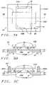
- FIG. 1Ashows a device 10 A comprising a first (PCB) Printed Circuit Board PB 1 composed of a conventional electrically insulating or dielectric material with a planar upper surface and a planar lower surfaces parallel to each other.
- a first (PCB) Printed Circuit Board PB 1composed of a conventional electrically insulating or dielectric material with a planar upper surface and a planar lower surfaces parallel to each other.
- On the upper surface of Printed Circuit Board PB 1are two chips CHA and CHB which are connected to the upper surface electrically and mechanically by solder balls SB to conventional pads not shown on the top surface of the printed circuit board PB 1 .
- Buried within the printed circuit board PB 1are a conductive ground plane BP and a conductive power plane PP, shown in this example, below the ground plane BP.
- Both the conductive ground plane BP and the conductive power plane PPare shown to be parallel with the upper and lower surface of the printed circuit board PB 1 . Modifications of the power plane are possible including multiple levels and variations from simple parallel structures into partially non-parallel arrangements with vias as will be well understood by those skilled in the art.
- the big solder balls BSBare adapted to be connected electrically and mechanically to a supporting element such as another printed circuit board, e.g. a larger circuit board (not shown) as will be well understood by those skilled in the art.
- Chips CHA and CHBare attached to the Printed Circuit Board PB 1 by the flip-chip method, as will be well understood by those skilled in the art of chip packaging.
- a bypass capacitor BC 1which is located below the bottom surface of the printed circuit board PB 1 on the exterior of printed circuit board PB 1 is connected directly at one end to the internal ground plane GP and is connected directly at the other terminal to the internal power plane PP as seen in FIG. 1A .
- the big solder balls BSB on the lower surface of the board PB 1provide added clearance for the capacitor BC 1 .
- the bypass capacitor BC 1can be located below the exterior of the lower surface of the printed circuit board PB 1 and below one or both of the chip CHA and chip CHB because the big solder balls BSB are tall enough to provide clearance for the bypass capacitor BC 1 (see FIG. 1A ).
- a ground bus GB and a power bus PBare formed on the top surface of board PB 1 .
- Another bypass capacitor BC 1 ′is shown in the right end of the board PB 1 with one terminal connected to the ground bus GB and another terminal connected to the power bus PB (see FIG. 1A ).
- Printed circuit board PB 1is a multi-layer printed circuit board.
- the small solder balls SB connected to chip CHA and chip CHBare connected to the bio solder balls BSB through the routing of the printed circuits and vias (not shown) on the printed circuit board PB 1 , as will be well understood by those skilled in the art of chip packaging.
- FIG. 1Bshows a variation of the device of FIG. 1A comprising a modified device 10 B.
- Device 10 Bincludes a printed circuit board PB 2 , which is basically the same as board PB 1 ( FIG. 1A ) except that the connection of elements thereto is somewhat different and ground bus GB and power bus PB are omitted.
- Chip CHC and chip CHDwhich are located on the top surface of board PB 2 , are narrower leaving space to locate the bypass capacitor BC 2 therebetween above the exterior of the upper surface of the printed circuit board PB 2 in FIG. 1B .
- Bypass capacitor BC 2is connected directly at one end to a buried, internal ground plane GP and at the other terminal of the bypass capacitor BC 2 is connected directly to a buried, internal power plane PP as described above with respect to FIG. 1A .
- the small solder balls SBare located on the bottom of the board PB 2 (in place of the big solder balls BSB or FIG. 1A ) since there is no need for the extra clearance required in FIG. 1A for location of the bypass capacitor BC 1 .
- FIG. 1Cshows a device 10 C which is a modification of the devices 10 A of FIG. 1A and 10B of FIG. 1B .
- the device 10 Cincludes a third printed circuit board PB 3 , different from the board PB 1 of FIG. 1A except that the elements connected thereto are somewhat different.
- board PB 3includes no buried ground plane and no buried power plane.
- Chip CHE and chip CHFwhich are located on the top surface of board PB 2 , are narrower leaving space to locate the bypass capacitor BC 2 therebetween on the upper surface of board PB 2 .
- Chip CHE and chip CHFwhich are located on the top surface of board PB 2 , are narrower than chips CHA and CHB, leaving space to locate the bypass capacitor BC 2 therebetween on the upper surface of board PB 3 .
- Bypass capacitor BC 3is connected at one end to the around bus GB and at the other terminal to the power bus PP.
- small solder balls SBare located on the bottom of the board PB 2 (in place of the big solder balls BSB or FIG. 1A ).
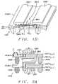
- FIG. 1Dshows a perspective view of a modification of FIG. 1B with two chips, chip CHC′ and chip CHD′ on top of the printed circuit board PCB 1 along with the bypass capacitor BC 3 shown located above the exterior of the top surface of the printed circuit board PCB 1 between chips CHC′, CHD′.
- a wide metal conductor line comprising a power bus WM 1is formed on the surface of the printed circuit board PCB 1 , as shown in FIG. 1D , connecting to one terminal of the capacitor BC 3 and the other wide metal line comprising ground bus WM 2 on the surface of the printed circuit board PCB 1 , connecting to the other terminal of the capacitor BC 3 .
- the wide metal line power bus WM 1connects by vias to some solder balls SB in the middle of chips CHC′ and CHD′ and down to the buried, internal power plane PP, as shown in FIG. 1D .
- the wide metal line ground bus WM 2connects by other vias to other solder balls SB on the inner edges of chips CHC′ and CHD′, and down to the buried, internal ground plane GP, as shown in FIG. 1D .
- Viasare conductors as will be well understood by those skilled in the art.
- FIG. 2Ashows a device 20 A which is a modification of FIG. 1A with two stacked Printed Circuit Boards PCB 2 and PCB 3 (similar to boards PB 1 ) with an plurality of big solder balls BSB on the periphery of the bottom of the boards PCB 2 and PCB 3 , with a buried, internal ground plane GP at voltage Vss and a buried, internal power plane PP at voltage Vcc as shown and as described above with respect to FIG. 1A .
- the upper Printed Circuit Board PCB 3is connected to the lower Printed Circuit Board PCB 2 by means of several big solder balls BSB which interconnect electrically and mechanically between the lower surface of upper board PCB 3 and lower board PCB 2 as is well understood by those skilled in the art by means of conductive mounting pads, conductors and vias not shown for convenience of illustration.
- Chips CH 1 and CH 2are supported on the bottom and top respectively of the lower board PCB 2 .
- Chips CH 1 and CH 2are connected electrically and mechanically by solder balls SB to conventional pads not shown on the bottom surface and top surface of the printed circuit board board PCB 2 respectively.
- two bottom-and-top mounted chips CH 3 and CH 4are supported on the bottom and top respectively of lower board PCB 2 , and chips CH 3 and CH 4 which are connected electrically and mechanically by solder balls SB to conventional pads not shown on the bottom surface and top surface of the lower printed circuit board board PCB 2 .
- An external bypass capacitor Cis formed on the left of the top surface of board PCB 3 .
- the externally located bypass capacitor Cis shown in FIG. 2A located close to the chips CH 3 and CH 4 .
- Bypass capacitoralso can be mounted on the left upper surface of lower board PCB 2 .
- Bypass capacitor Chas one terminal shown connected directly to the buried, internal ground plane GP in the upper board PCB 3 and at the other terminal shown connected directly to the buried, internal power plane PP in the upper board PCB 3 .
- the circuitsare similar to those as discussed in FIG. 1B .
- FIG. 2Bshows device 20 B which is a modification of the device 20 A of FIG. 2A which has been expanded to include several additional printed circuit boards PBC 4 and PCB 5 which have been stacked on top of upper board PCB 3 carrying chips CH 5 and CH 6 shown mounted bottom-and-top and carrying chips CH 7 and CH 8 shown mounted bottom-and-top respectively with the big solder balls BSB supporting each printed circuit board, with printed circuit board PCB 4 supported on printed circuit board PCB 3 and printed circuit board PCB 5 supported on printed circuit board PCB 4 in like manner to the boards of FIG. 2A .
- the lower-most printed circuit board PCB 2is shown supported on a moderate size set of enlarged solder balls SB.
- a bypass capacitor Cwhich is shown located above the exterior of the top surface of printed circuit board PCB 5 at the left end thereof, has one terminal shown connected directly to the buried, internal ground plane GP and is shown connected directly at the other terminal to the buried, internal power plane PP.
- FIG. 2Cshows a modification of the device of FIG. 2A which has been modified to include a chip CH 3 on the top of the upper printed circuit board PCB 3 ′ without big solder balls between the upper and lower printed circuit boards.
- FIG. 2Cshows a device 20 C which is another modification of the device 20 A of FIG. 2A which has been simplified to include top and bottom chips CH 1 and CH 2 on the lower board PCB 2 with a single chip CH 3 on the top surface of the upper board PBC 3 ′ with smaller solder balls SB interconnecting between the bottom of the upper printed circuit board PCB 3 ′ and the top of lower board PCB 2 and connected to the bottom of the lower board PCB 2 .
- a bypass capacitor Cshown located externally above the top surface of the upper printed circuit board PCB 3 ′ at the left end thereof, has one terminal shown connected directly to the buried, internal ground plane GP and at the other terminal is shown connected directly to the buried, internal power plane PP of the upper printed circuit board PCB 3 ′.
- FIG. 2Dshows a device 20 D which is a modification of the device 20 B of FIG. 2B which has been modified to use gold bumps GB to support the chips CH 1 -CH 8 to the respective printed circuit boards PBC 2 to PCB 5 .
- An external bypass capacitor Cis shown located above the top surface of a printed circuit board PCB 5 at the left end thereof.
- the external bypass capacitor Chas one terminal shown connected directly to the buried, internal ground plane GP and, as shown, has the other terminal connected directly to the buried, internal power plane PP thereof shown inside the printed circuit board PCB 5 .
- FIG. 2Eshows a device 20 E which is another modification of the device 20 C of FIG. 2C which has been modified to use gold bumps GB to support the chips CH 1 -CH 3 on the respective lower and upper printed circuit boards PBC 2 and PCB 3 ′.
- An external bypass capacitor Cis shown located above the top surface of the upper printed circuit board PCB 3 ′ at the left end thereof, and it has one terminal shown connected directly to the buried, internal ground plane GP and at the other terminal shown connected directly to the buried, internal power plane PP thereof.
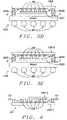
- FIG. 3Ashows a plan view of a chip-on-chip structure in accordance with this invention where a printed circuit board PCB 6 has a window W formed therethrough (board PCB 6 ) in the center of FIG. 3A .
- Window Wis shown to have a longer vertical height than the horizontal width.
- the board PBC 6is the substrate of a Ball Grid Array (BGA) package.
- BGABall Grid Array
- a primary, upper chip CH 5is formed above the board PCB 6 , covering the central portion of window W having its greater length transverse to the window W thereby bridging the window W across the width of the window W. That is to say that primary chip CH 5 extends on the left and right beyond window W over board PCB 6 across the (narrower) width of the window W.
- the secondary chip CG 16is supported in a chip-on-chip connected by the lower surface of chip primary CH 5 .
- secondary chip CH 6is located inside the space provided by window W in the printed circuit board PCB 6 .
- the chips CH 5 and CH 6are shown to be the same size, i.e. primary chips CH 5 is as long and as wide as secondary chip CH 6 but they are rotated in orientation by about 90 degrees.
- a bypass capacitor BCis located on the top surface of printed circuit board PCB 6 and as described above, the opposing terminals of capacitor BC are connected to a ground plane GP and the power plane PP, respectively, inside the board PCB 6 .
- FIG. 3Bis a sectional view taken along line 3 B- 3 B in FIG. 3A .
- the chip-on-chip relationship between primary chip CH 5 and secondary chip CH 6is seen.
- Pads P on the upper surface of secondary chip CH 6are connected electrically and mechanically by solder balls SB to interconnect pads P on the confronting surfaces of the primary, upper chip CH 5 .
- the lower surface of primary chip CH 5aside from secondary chip CH 6 , is connected to pads P on the upper surface of Printed Circuit Board PCB 6 .
- the printed circuit board PCB 3has solder balls SB and pads P located on the lower surface thereof which are adapted to be connected to another circuit board (not shown).
- FIG. 3Cis a modification of FIG. 3B in which the printed circuit board PCB 6 ′ has outboard connection pads P located aside from chip CH 5 supporting large solder balls BSB which are adapted to connect the board PCB 6 ′ to another circuit board (not shown) as shown by examples in FIGS. 2A , 2 B and 2 D above.
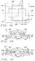
- FIG. 3Dshows a chip-on-chip structure wherein pads P on the top surface of a lower, secondary chip CH 17 is bonded to a plurality of solder balls SB which are also bonded to the bottom of upper, primary chip CH 8 .
- chip CH 8is carried by a plurality of big solder balls BSB secured to bottom surface of chip CH 8 on the ends thereof with the width of secondary chip CH 7 shown in FIG. 3D being narrower than the length of primary chip CH 8 as in FIGS. 3A and 3B .
- the big solder balls BSBare supported on the bottom ends thereof, below the chips C 7 and CH 8 , by pads P on a ball grid array substrate BGAS which is supported by a grid array of solder balls BG.
- FIG. 3Eshows a chip-on-chip structure wherein the pads on the top surface of secondary chip C 9 is bonded to a plurality of gold bumps GB bonded to pads on the bottom of primary chip CH 10 .
- chip CH 10is carried by a plurality of bio solder balls BSB secured to bottom surface of chip CH 10 on the ends thereof with the width of chip CH 9 being narrower than the length of chip CH 10 as in FIGS. 3A and 3B .
- the big solder balls BSBare supported on the bottom ends thereof, below the chips CH 7 and CH 8 , by pads P on a ball grid array substrate BGAS which is supported by a grid array of solder balls BG.
- FIG. 4shows a chip-on-chip) interconnection of a primary semiconductor chip CH 11 and a secondary chip CH 12 .
- the primary chiphas a top surface which is bonded to (,old bonds GB which in turn are bonded to pads P on the bottom surface of the secondary chip CH 12 forming chip-on-chip connections between the bottom surface of the secondary chip CH 12 and the top surface of the primary chip CH 11 .
- gold bond connectionsare formed aside from tie secondary chip to Tape Automated Bonding (TAB) copper leads CL.
- TABTape Automated Bonding
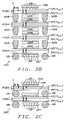
- FIG. 5Ashows a plan view of a plural chip to single chip chip-on-chip structure in accordance with this invention where a printed circuit board PCB 4 has a window W formed through board PCB 4 in the center of FIG. 5A .
- a pair of primacy chips CH 7 and CH 8are formed above the printed circuit board PCB 4 covering the central portion of window W.
- primary chip CH 7extends on the left beyond window W over the top surface board PCB 4 to which it is connected by solder balls B and pads P, similarly to the solder bonds described above.
- primary chip CH 8extends on the tight beyond window W over board PCB 4 to which it is also connected by solder balls B and pads P.
- a secondary chip CH 9is located below chip CH 7 and CH 8 inside the window W in the board PCB 4 .
- a bypass capacitor BCis located on the top surface of board PCB 4 .
- the pads X of bypass capacitor BCare connected to the ground plane GP and the power plane PP as explained in the above described embodiments of this invention.
- FIG. 5Bis a sectional view taken along line 4 B- 4 B in FIG. 5A .
- connection pads P on the upper surface of chip CH 9are bonded by solder balls SLD electrically and mechanically to interconnect pads P on the confronting surfaces of upper chips CH 7 /CH 8 .
- the lower surfaces of chips CH 7 /CH 8aside from chip CH 9 , are connected to pads P on the upper surface of Printed Circuit Board PCB 4 .
- the printed circuit board PCB 4has outboard solder balls S 13 and pads P located on the lower surface thereof which are adapted to be connected to another circuit board (not shown).
- Board PCB 4is a substrate of a BGA type package.
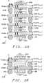
- FIG. 5Cis a slight modification of FIG. 5B in which outboard connection pads P and big solder balls BSB has been added to the top surface of printed circuit board PCB 4 ′.
- the big solder balls BSB on the top surface of the board PCB 4 ′, which are available for external connections,are located aside from chips CH 7 and CH 8 with big solder balls BSB which are adapted to connect the board PCB 4 ′ to another circuit board (not shown).
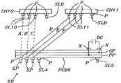
- FIG. 6shows a sectional view of a circuit board PCB 5 which has a number of pads P to which one solder pin CP, two solder pin SP, and two solder pins SL 4 and SL 5 are connected respectively as shown.
- the solder in CPfunctions as a control pin.
- the solder pins SPfunction as selection pins.
- Chips CH 10 and C 11are shown connected by dotted lines ABC and DEF between the pads for pins CP and SP and pins SL 10 and SL 11 on pads P on the bottom of chips CH 10 and CH 11 respectively. Additional bumps SLD are also connected to the chips by bonding to pads P.
- An external bypass capacitor BCis shown located above the top surface of the circuit board PCB 5 .
- the pads X of the external bypass capacitor BCare shown to be connected to the circuit board PCB 5 with one pad X shown being connected directly to the buried, internal ground plane GP and with the other pad X shown being connected directly to the buried, internal power plane PP as explained in the above described embodiments of this invention.
- the control solder pin CPis electrically connected to a pin SL 10 formed on the chip CH 10 and a pin SL 11 formed on the chip CH 11 , by the connections represented by the dotted line A and the dotted line D, respectively.
- the selection solder balls SPare electrically connected to the respective pins SL 10 formed on the chip CH 10 , by the connections represented by the dotted lines B and C, and to the respective pins SL 11 formed on the chip CH 11 , by the connections represented by the dotted lines E and F.
- Chips CH 10 and CH 11are connected to the board PCB 5 by the flip-chip method.
- the control solder pins of chips CH 10 and CH 11are connected to the control solder pin CP of board PCB 5 through first interconnection metal lines of board PCB 5 .
- the selection solder pins of chips CH 10 and CH 11are connected to the selection solder pin SP of board PCB 5 through other interconnection metal lines of board PCB 5 .
- this diecan be x4, x8, x16 or x32.
- the meaning of the x4 optionis that the width of the data is 4 bits in an integrated circuit memory.
- FIG. 6shows the inventive concept that optional functions can be provided in a multiple chip package made in accordance with this invention.
- optional functionsare possible only on a single chip level, whereas with the configuration shown in FIG. 6 and previous drawings, the function of a chip can be fixed after completion of the packaging process.
- FIG. 6 and the embodiments from FIG. 1A to FIG. 4C and FIG. 5Aall have a bypass capacitor. All of the printed circuit boards include a ground plane and a power plane. The bypass capacitors are connected between the ground plane and the power plane.
- the pad options illustrated by FIG. 6can be employed in the embodiments from FIG. 1A to FIG. 4C .
- a bonding option for a multiple chip packageis provided.
- Methods of mounting discrete chips on a chip package or multi-chip packagewhich may include a bypass capacitor, a ground plane and a power plane.
- a control circuit design in the single chipprovides for function selection.
- the bypass capacitoris packed in a package or in combination chip package.
- the bypass capacitoris connected to the ground plane and the power plane of the substrate of the package.
- a big solder ballis employed for packages when the bypass capacitor is located on the same surface with the solder balls which are adapted to be connected to another circuit board.
- a problem solved by this inventionis reduction of the inventory of several products with different functions.
- This inventionserves to eliminate I/O noise.
Landscapes
- Engineering & Computer Science (AREA)
- Microelectronics & Electronic Packaging (AREA)
- Power Engineering (AREA)
- Physics & Mathematics (AREA)
- Condensed Matter Physics & Semiconductors (AREA)
- General Physics & Mathematics (AREA)
- Computer Hardware Design (AREA)
- Electromagnetism (AREA)
- Structures For Mounting Electric Components On Printed Circuit Boards (AREA)
Abstract
Description
Claims (14)
Priority Applications (3)
| Application Number | Priority Date | Filing Date | Title |
|---|---|---|---|
| US10/437,333US7468551B2 (en) | 2000-05-19 | 2003-05-13 | Multiple chips bonded to packaging structure with low noise and multiple selectable functions |
| US12/269,053US8148806B2 (en) | 2000-05-19 | 2008-11-12 | Multiple chips bonded to packaging structure with low noise and multiple selectable functions |
| US12/269,054US20090056988A1 (en) | 2000-05-19 | 2008-11-12 | Multiple chips bonded to packaging structure with low noise and multiple selectable functions |
Applications Claiming Priority (2)
| Application Number | Priority Date | Filing Date | Title |
|---|---|---|---|
| US09/573,955US7247932B1 (en) | 2000-05-19 | 2000-05-19 | Chip package with capacitor |
| US10/437,333US7468551B2 (en) | 2000-05-19 | 2003-05-13 | Multiple chips bonded to packaging structure with low noise and multiple selectable functions |
Related Parent Applications (1)
| Application Number | Title | Priority Date | Filing Date |
|---|---|---|---|
| US09/573,955DivisionUS7247932B1 (en) | 2000-05-19 | 2000-05-19 | Chip package with capacitor |
Related Child Applications (2)
| Application Number | Title | Priority Date | Filing Date |
|---|---|---|---|
| US12/269,053ContinuationUS8148806B2 (en) | 2000-05-19 | 2008-11-12 | Multiple chips bonded to packaging structure with low noise and multiple selectable functions |
| US12/269,054ContinuationUS20090056988A1 (en) | 2000-05-19 | 2008-11-12 | Multiple chips bonded to packaging structure with low noise and multiple selectable functions |
Publications (2)
| Publication Number | Publication Date |
|---|---|
| US20030201545A1 US20030201545A1 (en) | 2003-10-30 |
| US7468551B2true US7468551B2 (en) | 2008-12-23 |
Family
ID=24294074
Family Applications (8)
| Application Number | Title | Priority Date | Filing Date |
|---|---|---|---|
| US09/573,955Expired - LifetimeUS7247932B1 (en) | 2000-05-19 | 2000-05-19 | Chip package with capacitor |
| US10/371,505Expired - LifetimeUS7045901B2 (en) | 2000-05-19 | 2003-02-21 | Chip-on-chip connection with second chip located in rectangular open window hole in printed circuit board |
| US10/371,506Expired - LifetimeUS6791192B2 (en) | 2000-05-19 | 2003-02-21 | Multiple chips bonded to packaging structure with low noise and multiple selectable functions |
| US10/420,595Expired - LifetimeUS7205646B2 (en) | 2000-05-19 | 2003-04-22 | Electronic device and chip package |
| US10/437,355Expired - LifetimeUS6768208B2 (en) | 2000-05-19 | 2003-05-13 | Multiple chips bonded to packaging structure with low noise and multiple selectable functions |
| US10/437,333Expired - Fee RelatedUS7468551B2 (en) | 2000-05-19 | 2003-05-13 | Multiple chips bonded to packaging structure with low noise and multiple selectable functions |
| US12/269,054AbandonedUS20090056988A1 (en) | 2000-05-19 | 2008-11-12 | Multiple chips bonded to packaging structure with low noise and multiple selectable functions |
| US12/269,053Expired - Fee RelatedUS8148806B2 (en) | 2000-05-19 | 2008-11-12 | Multiple chips bonded to packaging structure with low noise and multiple selectable functions |
Family Applications Before (5)
| Application Number | Title | Priority Date | Filing Date |
|---|---|---|---|
| US09/573,955Expired - LifetimeUS7247932B1 (en) | 2000-05-19 | 2000-05-19 | Chip package with capacitor |
| US10/371,505Expired - LifetimeUS7045901B2 (en) | 2000-05-19 | 2003-02-21 | Chip-on-chip connection with second chip located in rectangular open window hole in printed circuit board |
| US10/371,506Expired - LifetimeUS6791192B2 (en) | 2000-05-19 | 2003-02-21 | Multiple chips bonded to packaging structure with low noise and multiple selectable functions |
| US10/420,595Expired - LifetimeUS7205646B2 (en) | 2000-05-19 | 2003-04-22 | Electronic device and chip package |
| US10/437,355Expired - LifetimeUS6768208B2 (en) | 2000-05-19 | 2003-05-13 | Multiple chips bonded to packaging structure with low noise and multiple selectable functions |
Family Applications After (2)
| Application Number | Title | Priority Date | Filing Date |
|---|---|---|---|
| US12/269,054AbandonedUS20090056988A1 (en) | 2000-05-19 | 2008-11-12 | Multiple chips bonded to packaging structure with low noise and multiple selectable functions |
| US12/269,053Expired - Fee RelatedUS8148806B2 (en) | 2000-05-19 | 2008-11-12 | Multiple chips bonded to packaging structure with low noise and multiple selectable functions |
Country Status (1)
| Country | Link |
|---|---|
| US (8) | US7247932B1 (en) |
Cited By (6)
| Publication number | Priority date | Publication date | Assignee | Title |
|---|---|---|---|---|
| US20090233402A1 (en)* | 2008-03-11 | 2009-09-17 | Taiwan Semiconductor Manufacturing Co., Ltd. | Wafer level ic assembly method |
| US20100096659A1 (en)* | 2007-03-09 | 2010-04-22 | Sanyo Electric Co., Ltd. | Semiconductor device and method of manufacturing the same |
| US8148806B2 (en) | 2000-05-19 | 2012-04-03 | Megica Corporation | Multiple chips bonded to packaging structure with low noise and multiple selectable functions |
| US8188497B2 (en) | 2007-02-02 | 2012-05-29 | Sanyo Semiconductor Co., Ltd. | Semiconductor device and method of manufacturing the same |
| US8599596B2 (en)* | 2009-07-29 | 2013-12-03 | Elpida Memory, Inc. | Semiconductor device |
| US20170017594A1 (en)* | 2009-05-26 | 2017-01-19 | Rambus Inc. | Stacked Semiconductor Device Assembly in Computer System |
Families Citing this family (202)
| Publication number | Priority date | Publication date | Assignee | Title |
|---|---|---|---|---|
| US6826827B1 (en)* | 1994-12-29 | 2004-12-07 | Tessera, Inc. | Forming conductive posts by selective removal of conductive material |
| US6525414B2 (en)* | 1997-09-16 | 2003-02-25 | Matsushita Electric Industrial Co., Ltd. | Semiconductor device including a wiring board and semiconductor elements mounted thereon |
| US6297548B1 (en) | 1998-06-30 | 2001-10-02 | Micron Technology, Inc. | Stackable ceramic FBGA for high thermal applications |
| US7102892B2 (en)* | 2000-03-13 | 2006-09-05 | Legacy Electronics, Inc. | Modular integrated circuit chip carrier |
| US6713854B1 (en)* | 2000-10-16 | 2004-03-30 | Legacy Electronics, Inc | Electronic circuit module with a carrier having a mounting pad array |
| US7337522B2 (en)* | 2000-10-16 | 2008-03-04 | Legacy Electronics, Inc. | Method and apparatus for fabricating a circuit board with a three dimensional surface mounted array of semiconductor chips |
| JP4422323B2 (en)* | 2000-12-15 | 2010-02-24 | 株式会社ルネサステクノロジ | Semiconductor device |
| WO2002074024A2 (en)* | 2001-03-14 | 2002-09-19 | Legacy Electronics, Inc. | A method and apparatus for fabricating a circuit board with a three dimensional surface mounted array of semiconductor chips |
| US6707684B1 (en)* | 2001-04-02 | 2004-03-16 | Advanced Micro Devices, Inc. | Method and apparatus for direct connection between two integrated circuits via a connector |
| US6762487B2 (en)* | 2001-04-19 | 2004-07-13 | Simpletech, Inc. | Stack arrangements of chips and interconnecting members |
| US6613606B1 (en) | 2001-09-17 | 2003-09-02 | Magic Corporation | Structure of high performance combo chip and processing method |
| GB2385984B (en)* | 2001-11-07 | 2006-06-28 | Micron Technology Inc | Semiconductor package assembly and method for electrically isolating modules |
| JP4054200B2 (en)* | 2002-02-19 | 2008-02-27 | 松下電器産業株式会社 | Semiconductor memory device |
| US7046522B2 (en)* | 2002-03-21 | 2006-05-16 | Raymond Jit-Hung Sung | Method for scalable architectures in stackable three-dimensional integrated circuits and electronics |
| JP2003298305A (en)* | 2002-03-28 | 2003-10-17 | Fujitsu Quantum Devices Ltd | High-frequency switch and electronic device using the same |
| JP2003324183A (en)* | 2002-05-07 | 2003-11-14 | Mitsubishi Electric Corp | Semiconductor device |
| US20050104211A1 (en)* | 2002-05-07 | 2005-05-19 | Shinji Baba | Semiconductor device having semiconductor chips mounted on package substrate |
| US7294928B2 (en)* | 2002-09-06 | 2007-11-13 | Tessera, Inc. | Components, methods and assemblies for stacked packages |
| US7495326B2 (en)* | 2002-10-22 | 2009-02-24 | Unitive International Limited | Stacked electronic structures including offset substrates |
| TWI236117B (en)* | 2003-02-26 | 2005-07-11 | Advanced Semiconductor Eng | Semiconductor package with a heat sink |
| JP4096774B2 (en)* | 2003-03-24 | 2008-06-04 | セイコーエプソン株式会社 | SEMICONDUCTOR DEVICE, ELECTRONIC DEVICE, ELECTRONIC DEVICE, SEMICONDUCTOR DEVICE MANUFACTURING METHOD, AND ELECTRONIC DEVICE MANUFACTURING METHOD |
| US7047515B1 (en)* | 2003-04-04 | 2006-05-16 | Extreme Networks | Method for selecting and placing bypass capacitors on multi-layer printed circuit boards |
| TWI231591B (en)* | 2003-04-23 | 2005-04-21 | Advanced Semiconductor Eng | Multi-chips stacked package |
| JP3858854B2 (en)* | 2003-06-24 | 2006-12-20 | 富士通株式会社 | Multilayer semiconductor device |
| DE10333800B3 (en)* | 2003-07-24 | 2004-10-28 | Infineon Technologies Ag | Semiconductor component e.g. bridge circuit, using chip-on-chip technology with end sections of electrical terminal bonding wires as contact region between lower and upper semiconductor elements |
| US6994918B2 (en)* | 2003-08-12 | 2006-02-07 | Johnson Morgan T | Selective application of conductive material to circuit boards by pick and place |
| WO2005022965A2 (en)* | 2003-08-29 | 2005-03-10 | Thermalworks, Inc. | Expansion constrained die stack |
| US7180165B2 (en) | 2003-09-05 | 2007-02-20 | Sanmina, Sci Corporation | Stackable electronic assembly |
| US20050112842A1 (en)* | 2003-11-24 | 2005-05-26 | Kang Jung S. | Integrating passive components on spacer in stacked dies |
| KR100610462B1 (en)* | 2004-02-20 | 2006-08-08 | 엔이씨 도낀 가부시끼가이샤 | Solid electrolytic capacitor, transmission-line device, method of producing the same, and composite electronic component using the same |
| US7528473B2 (en)* | 2004-03-19 | 2009-05-05 | Renesas Technology Corp. | Electronic circuit, a semiconductor device and a mounting substrate |
| US7453157B2 (en)* | 2004-06-25 | 2008-11-18 | Tessera, Inc. | Microelectronic packages and methods therefor |
| KR100573302B1 (en)* | 2004-10-07 | 2006-04-24 | 삼성전자주식회사 | Package Stack Using Wire Bonding and Manufacturing Method Thereof |
| JP4738996B2 (en)* | 2004-12-13 | 2011-08-03 | キヤノン株式会社 | Semiconductor device |
| WO2006076381A2 (en) | 2005-01-12 | 2006-07-20 | Legacy Electronics, Inc. | Radial circuit board, system, and methods |
| TWI253701B (en)* | 2005-01-21 | 2006-04-21 | Via Tech Inc | Bump-less chip package |
| WO2006080351A1 (en)* | 2005-01-25 | 2006-08-03 | Matsushita Electric Industrial Co., Ltd. | Semiconductor device and its manufacturing method |
| US7545031B2 (en)* | 2005-04-11 | 2009-06-09 | Stats Chippac Ltd. | Multipackage module having stacked packages with asymmetrically arranged die and molding |
| TWI264887B (en)* | 2005-05-05 | 2006-10-21 | Universal Scient Ind Co Ltd | Small-form-factor wireless communication module and manufacturing method thereof |
| JP4758678B2 (en)* | 2005-05-17 | 2011-08-31 | ルネサスエレクトロニクス株式会社 | Semiconductor device |
| US7675151B1 (en)* | 2005-06-01 | 2010-03-09 | Rockwell Collins, Inc. | Silicon-based packaging for electronic devices |
| US7638866B1 (en)* | 2005-06-01 | 2009-12-29 | Rockwell Collins, Inc. | Stacked packaging designs offering inherent anti-tamper protection |
| US8089795B2 (en) | 2006-02-09 | 2012-01-03 | Google Inc. | Memory module with memory stack and interface with enhanced capabilities |
| US8438328B2 (en) | 2008-02-21 | 2013-05-07 | Google Inc. | Emulation of abstracted DIMMs using abstracted DRAMs |
| US8130560B1 (en) | 2006-11-13 | 2012-03-06 | Google Inc. | Multi-rank partial width memory modules |
| US8796830B1 (en) | 2006-09-01 | 2014-08-05 | Google Inc. | Stackable low-profile lead frame package |
| US20080028136A1 (en) | 2006-07-31 | 2008-01-31 | Schakel Keith R | Method and apparatus for refresh management of memory modules |
| US8359187B2 (en) | 2005-06-24 | 2013-01-22 | Google Inc. | Simulating a different number of memory circuit devices |
| US10013371B2 (en) | 2005-06-24 | 2018-07-03 | Google Llc | Configurable memory circuit system and method |
| US8055833B2 (en) | 2006-10-05 | 2011-11-08 | Google Inc. | System and method for increasing capacity, performance, and flexibility of flash storage |
| US9542352B2 (en) | 2006-02-09 | 2017-01-10 | Google Inc. | System and method for reducing command scheduling constraints of memory circuits |
| US7386656B2 (en) | 2006-07-31 | 2008-06-10 | Metaram, Inc. | Interface circuit system and method for performing power management operations in conjunction with only a portion of a memory circuit |
| US9507739B2 (en) | 2005-06-24 | 2016-11-29 | Google Inc. | Configurable memory circuit system and method |
| US8081474B1 (en) | 2007-12-18 | 2011-12-20 | Google Inc. | Embossed heat spreader |
| US8111566B1 (en) | 2007-11-16 | 2012-02-07 | Google, Inc. | Optimal channel design for memory devices for providing a high-speed memory interface |
| US8386722B1 (en) | 2008-06-23 | 2013-02-26 | Google Inc. | Stacked DIMM memory interface |
| US8244971B2 (en) | 2006-07-31 | 2012-08-14 | Google Inc. | Memory circuit system and method |
| US8041881B2 (en) | 2006-07-31 | 2011-10-18 | Google Inc. | Memory device with emulated characteristics |
| US8327104B2 (en) | 2006-07-31 | 2012-12-04 | Google Inc. | Adjusting the timing of signals associated with a memory system |
| US9171585B2 (en) | 2005-06-24 | 2015-10-27 | Google Inc. | Configurable memory circuit system and method |
| US8077535B2 (en) | 2006-07-31 | 2011-12-13 | Google Inc. | Memory refresh apparatus and method |
| US8060774B2 (en) | 2005-06-24 | 2011-11-15 | Google Inc. | Memory systems and memory modules |
| US8090897B2 (en) | 2006-07-31 | 2012-01-03 | Google Inc. | System and method for simulating an aspect of a memory circuit |
| KR101377305B1 (en) | 2005-06-24 | 2014-03-25 | 구글 인코포레이티드 | An integrated memory core and memory interface circuit |
| US20080082763A1 (en) | 2006-10-02 | 2008-04-03 | Metaram, Inc. | Apparatus and method for power management of memory circuits by a system or component thereof |
| US8397013B1 (en) | 2006-10-05 | 2013-03-12 | Google Inc. | Hybrid memory module |
| US8335894B1 (en) | 2008-07-25 | 2012-12-18 | Google Inc. | Configurable memory system with interface circuit |
| US7609567B2 (en)* | 2005-06-24 | 2009-10-27 | Metaram, Inc. | System and method for simulating an aspect of a memory circuit |
| KR100665217B1 (en)* | 2005-07-05 | 2007-01-09 | 삼성전기주식회사 | Semiconductor Multichip Package |
| KR100914552B1 (en)* | 2005-07-25 | 2009-09-02 | 삼성전자주식회사 | semiconductor memory device and memory module including it |
| JP5116268B2 (en)* | 2005-08-31 | 2013-01-09 | キヤノン株式会社 | Multilayer semiconductor device and manufacturing method thereof |
| WO2007028109A2 (en) | 2005-09-02 | 2007-03-08 | Metaram, Inc. | Methods and apparatus of stacking drams |
| JP4930970B2 (en)* | 2005-11-28 | 2012-05-16 | ルネサスエレクトロニクス株式会社 | Multi-chip module |
| JPWO2007069606A1 (en) | 2005-12-14 | 2009-05-21 | 新光電気工業株式会社 | Manufacturing method of chip embedded substrate |
| US9632929B2 (en) | 2006-02-09 | 2017-04-25 | Google Inc. | Translating an address associated with a command communicated between a system and memory circuits |
| JP4325630B2 (en)* | 2006-03-14 | 2009-09-02 | ソニー株式会社 | 3D integration device |
| JP5285842B2 (en)* | 2006-04-13 | 2013-09-11 | パナソニック株式会社 | Integrated circuit mounting board and power line communication device |
| US7462509B2 (en)* | 2006-05-16 | 2008-12-09 | International Business Machines Corporation | Dual-sided chip attached modules |
| TWI336913B (en)* | 2006-07-18 | 2011-02-01 | Via Tech Inc | A chip and manufacturing method and application thereof |
| US7724589B2 (en) | 2006-07-31 | 2010-05-25 | Google Inc. | System and method for delaying a signal communicated from a system to at least one of a plurality of memory circuits |
| US20080079149A1 (en)* | 2006-09-28 | 2008-04-03 | Harry Hedler | Circuit board arrangement and method for producing a circuit board arrangement |
| US20080123318A1 (en)* | 2006-11-08 | 2008-05-29 | Atmel Corporation | Multi-component electronic package with planarized embedded-components substrate |
| US8110899B2 (en)* | 2006-12-20 | 2012-02-07 | Intel Corporation | Method for incorporating existing silicon die into 3D integrated stack |
| US20080150101A1 (en)* | 2006-12-20 | 2008-06-26 | Tessera, Inc. | Microelectronic packages having improved input/output connections and methods therefor |
| US20080157334A1 (en)* | 2006-12-29 | 2008-07-03 | Powertech Technology Inc. | Memory module for improving impact resistance |
| US7539034B2 (en)* | 2007-02-01 | 2009-05-26 | Qimonda North America Corp. | Memory configured on a common substrate |
| JP2008192725A (en)* | 2007-02-02 | 2008-08-21 | Spansion Llc | Semiconductor device, and method and apparatus for manufacturing the same |
| JP5137179B2 (en)* | 2007-03-30 | 2013-02-06 | ルネサスエレクトロニクス株式会社 | Semiconductor device |
| US20080258293A1 (en)* | 2007-04-17 | 2008-10-23 | Advanced Chip Engineering Technology Inc. | Semiconductor device package to improve functions of heat sink and ground shield |
| JP2008294423A (en)* | 2007-04-24 | 2008-12-04 | Nec Electronics Corp | Semiconductor device |
| JP5138277B2 (en)* | 2007-05-31 | 2013-02-06 | 京セラSlcテクノロジー株式会社 | Wiring board and manufacturing method thereof |
| US20080315406A1 (en)* | 2007-06-25 | 2008-12-25 | Jae Han Chung | Integrated circuit package system with cavity substrate |
| US8209479B2 (en) | 2007-07-18 | 2012-06-26 | Google Inc. | Memory circuit system and method |
| KR101481571B1 (en)* | 2007-08-21 | 2015-01-14 | 삼성전자주식회사 | Semiconductor package device and manufacturing method thereof |
| US7989229B2 (en)* | 2007-09-10 | 2011-08-02 | International Business Machines Corporation | Tactile surface inspection during device fabrication or assembly |
| US8080874B1 (en) | 2007-09-14 | 2011-12-20 | Google Inc. | Providing additional space between an integrated circuit and a circuit board for positioning a component therebetween |
| US8258614B2 (en)* | 2007-11-12 | 2012-09-04 | Stats Chippac Ltd. | Integrated circuit package system with package integration |
| US8144674B2 (en)* | 2008-03-27 | 2012-03-27 | Broadcom Corporation | Method and system for inter-PCB communications with wireline control |
| US8494030B2 (en)* | 2008-06-19 | 2013-07-23 | Broadcom Corporation | Method and system for 60 GHz wireless clock distribution |
| US7911388B2 (en)* | 2007-12-12 | 2011-03-22 | Broadcom Corporation | Method and system for configurable antenna in an integrated circuit package |
| US8270912B2 (en)* | 2007-12-12 | 2012-09-18 | Broadcom Corporation | Method and system for a transformer in an integrated circuit package |
| US7880677B2 (en)* | 2007-12-12 | 2011-02-01 | Broadcom Corporation | Method and system for a phased array antenna embedded in an integrated circuit package |
| US8106829B2 (en) | 2007-12-12 | 2012-01-31 | Broadcom Corporation | Method and system for an integrated antenna and antenna management |
| US8160498B2 (en)* | 2007-12-12 | 2012-04-17 | Broadcom Corporation | Method and system for portable data storage with integrated 60 GHz radio |
| US8583197B2 (en)* | 2007-12-12 | 2013-11-12 | Broadcom Corporation | Method and system for sharing antennas for high frequency and low frequency applications |
| US8855093B2 (en)* | 2007-12-12 | 2014-10-07 | Broadcom Corporation | Method and system for chip-to-chip communications with wireline control |
| KR100891537B1 (en)* | 2007-12-13 | 2009-04-03 | 주식회사 하이닉스반도체 | Substrate for semiconductor package and semiconductor package having same |
| US7539366B1 (en)* | 2008-01-04 | 2009-05-26 | International Business Machines Corporation | Optical transceiver module |
| US20090199277A1 (en)* | 2008-01-31 | 2009-08-06 | Norman James M | Credential arrangement in single-sign-on environment |
| KR100975654B1 (en)* | 2008-02-26 | 2010-08-17 | 한국과학기술원 | Solder joint structure with improved joint reliability between Cu-added Sn-3.5Ag solder and Ni-P lower metal layer |
| US8064936B2 (en)* | 2008-02-28 | 2011-11-22 | Broadcom Corporation | Method and system for a multistandard proxy |
| US8086190B2 (en)* | 2008-03-27 | 2011-12-27 | Broadcom Corporation | Method and system for reconfigurable devices for multi-frequency coexistence |
| US20090243741A1 (en)* | 2008-03-27 | 2009-10-01 | Ahmadreza Rofougaran | Method and system for processing signals via an oscillator load embedded in an integrated circuit (ic) package |
| US8198714B2 (en)* | 2008-03-28 | 2012-06-12 | Broadcom Corporation | Method and system for configuring a transformer embedded in a multi-layer integrated circuit (IC) package |
| SG142321A1 (en) | 2008-04-24 | 2009-11-26 | Micron Technology Inc | Pre-encapsulated cavity interposer |
| US8116676B2 (en)* | 2008-05-07 | 2012-02-14 | Broadcom Corporation | Method and system for inter IC communications utilizing a spatial multi-link repeater |
| US8310051B2 (en) | 2008-05-27 | 2012-11-13 | Mediatek Inc. | Package-on-package with fan-out WLCSP |
| US8093722B2 (en)* | 2008-05-27 | 2012-01-10 | Mediatek Inc. | System-in-package with fan-out WLCSP |
| US20090296310A1 (en)* | 2008-06-03 | 2009-12-03 | Azuma Chikara | Chip capacitor precursors, packaged semiconductors, and assembly method for converting the precursors to capacitors |
| US8014166B2 (en)* | 2008-09-06 | 2011-09-06 | Broadpak Corporation | Stacking integrated circuits containing serializer and deserializer blocks using through silicon via |
| US9293350B2 (en)* | 2008-10-28 | 2016-03-22 | Stats Chippac Ltd. | Semiconductor package system with cavity substrate and manufacturing method therefor |
| TW201023308A (en)* | 2008-12-01 | 2010-06-16 | Advanced Semiconductor Eng | Package-on-package device, semiconductor package and method for manufacturing the same |
| US8399983B1 (en)* | 2008-12-11 | 2013-03-19 | Xilinx, Inc. | Semiconductor assembly with integrated circuit and companion device |
| US8310061B2 (en)* | 2008-12-17 | 2012-11-13 | Qualcomm Incorporated | Stacked die parallel plate capacitor |
| US20100213589A1 (en)* | 2009-02-20 | 2010-08-26 | Tung-Hsien Hsieh | Multi-chip package |
| DE202010017690U1 (en) | 2009-06-09 | 2012-05-29 | Google, Inc. | Programming dimming terminating resistor values |
| US8227904B2 (en)* | 2009-06-24 | 2012-07-24 | Intel Corporation | Multi-chip package and method of providing die-to-die interconnects in same |
| KR101078734B1 (en)* | 2009-07-07 | 2011-11-02 | 주식회사 하이닉스반도체 | Semiconductor package and manufacturing method thereof, stack package using same |
| JP5646830B2 (en) | 2009-09-02 | 2014-12-24 | ルネサスエレクトロニクス株式会社 | Semiconductor device, method for manufacturing semiconductor device, and lead frame |
| US8837159B1 (en)* | 2009-10-28 | 2014-09-16 | Amazon Technologies, Inc. | Low-profile circuit board assembly |
| TWI501380B (en)* | 2010-01-29 | 2015-09-21 | Nat Chip Implementation Ct Nat Applied Res Lab | Three-dimensional soc structure stacking by multiple chip modules |
| US8222733B2 (en)* | 2010-03-22 | 2012-07-17 | Advanced Semiconductor Engineering, Inc. | Semiconductor device package |
| US8654538B2 (en)* | 2010-03-30 | 2014-02-18 | Ibiden Co., Ltd. | Wiring board and method for manufacturing the same |
| US8742603B2 (en)* | 2010-05-20 | 2014-06-03 | Qualcomm Incorporated | Process for improving package warpage and connection reliability through use of a backside mold configuration (BSMC) |
| TW201142998A (en)* | 2010-05-24 | 2011-12-01 | Mediatek Inc | System-in-package |
| US9137903B2 (en) | 2010-12-21 | 2015-09-15 | Tessera, Inc. | Semiconductor chip assembly and method for making same |
| US20120193788A1 (en) | 2011-01-31 | 2012-08-02 | Advanced Micro Devices, Inc. | Stacked semiconductor chips packaging |
| JP2012230961A (en)* | 2011-04-25 | 2012-11-22 | Elpida Memory Inc | Semiconductor device |
| US8927391B2 (en) | 2011-05-27 | 2015-01-06 | Taiwan Semiconductor Manufacturing Company, Ltd. | Package-on-package process for applying molding compound |
| US8963310B2 (en) | 2011-08-24 | 2015-02-24 | Tessera, Inc. | Low cost hybrid high density package |
| KR101774938B1 (en) | 2011-08-31 | 2017-09-06 | 삼성전자 주식회사 | Semiconductor package having supporting plate and method of forming the same |
| US8461676B2 (en) | 2011-09-09 | 2013-06-11 | Qualcomm Incorporated | Soldering relief method and semiconductor device employing same |
| US9101084B2 (en)* | 2011-12-30 | 2015-08-04 | Peking University Founder Group Co., Ltd. | Method of fabricating PCB board and PCB board |
| US8729697B2 (en)* | 2012-01-09 | 2014-05-20 | Infineon Technologies Ag | Sensor arrangement, a measurement circuit, chip-packages and a method for forming a sensor arrangement |
| US8686570B2 (en)* | 2012-01-20 | 2014-04-01 | Taiwan Semiconductor Manufacturing Company, Ltd. | Multi-dimensional integrated circuit structures and methods of forming the same |
| US8704384B2 (en) | 2012-02-17 | 2014-04-22 | Xilinx, Inc. | Stacked die assembly |
| US8704364B2 (en)* | 2012-02-08 | 2014-04-22 | Xilinx, Inc. | Reducing stress in multi-die integrated circuit structures |
| US8901730B2 (en) | 2012-05-03 | 2014-12-02 | Taiwan Semiconductor Manufacturing Company, Ltd. | Methods and apparatus for package on package devices |
| JP5474127B2 (en)* | 2012-05-14 | 2014-04-16 | 株式会社野田スクリーン | Semiconductor device |
| US8957512B2 (en) | 2012-06-19 | 2015-02-17 | Xilinx, Inc. | Oversized interposer |
| US8869088B1 (en) | 2012-06-27 | 2014-10-21 | Xilinx, Inc. | Oversized interposer formed from a multi-pattern region mask |
| US9026872B2 (en) | 2012-08-16 | 2015-05-05 | Xilinx, Inc. | Flexible sized die for use in multi-die integrated circuit |
| US9041176B2 (en) | 2012-10-08 | 2015-05-26 | Qualcomm Incorporated | Hybrid semiconductor module structure |
| TWI518878B (en)* | 2012-12-18 | 2016-01-21 | Murata Manufacturing Co | Laminated type electronic device and manufacturing method thereof |
| US8970023B2 (en) | 2013-02-04 | 2015-03-03 | Taiwan Semiconductor Manufacturing Company, Ltd. | Package structure and methods of forming same |
| CN203225947U (en)* | 2013-03-28 | 2013-10-02 | 富士康(昆山)电脑接插件有限公司 | Printed circuit board assembly |
| JP6199601B2 (en)* | 2013-05-01 | 2017-09-20 | ルネサスエレクトロニクス株式会社 | Semiconductor device |
| JP6045436B2 (en)* | 2013-05-02 | 2016-12-14 | ルネサスエレクトロニクス株式会社 | Electronic equipment |
| US9547034B2 (en) | 2013-07-03 | 2017-01-17 | Xilinx, Inc. | Monolithic integrated circuit die having modular die regions stitched together |
| US9653442B2 (en)* | 2014-01-17 | 2017-05-16 | Taiwan Semiconductor Manufacturing Company, Ltd. | Integrated circuit package and methods of forming same |
| US9685425B2 (en)* | 2014-01-28 | 2017-06-20 | Apple Inc. | Integrated circuit package |
| US10121768B2 (en) | 2015-05-27 | 2018-11-06 | Bridge Semiconductor Corporation | Thermally enhanced face-to-face semiconductor assembly with built-in heat spreader and method of making the same |
| US11291146B2 (en) | 2014-03-07 | 2022-03-29 | Bridge Semiconductor Corp. | Leadframe substrate having modulator and crack inhibiting structure and flip chip assembly using the same |
| US10354984B2 (en) | 2015-05-27 | 2019-07-16 | Bridge Semiconductor Corporation | Semiconductor assembly with electromagnetic shielding and thermally enhanced characteristics and method of making the same |
| US9806047B2 (en)* | 2014-03-31 | 2017-10-31 | Maxim Integrated Products, Inc. | Wafer level device and method with cantilever pillar structure |
| US9111846B1 (en)* | 2014-04-16 | 2015-08-18 | Gloval Unichip Corp. | Assembly structure for connecting multiple dies into a system-in-package chip and the method thereof |
| US9915869B1 (en) | 2014-07-01 | 2018-03-13 | Xilinx, Inc. | Single mask set used for interposer fabrication of multiple products |
| JP2016529716A (en)* | 2014-07-07 | 2016-09-23 | インテル アイピー コーポレーション | Package-on-package multilayer microelectronic structure |
| US9474154B2 (en) | 2014-07-18 | 2016-10-18 | Starkey Laboratories, Inc. | Reflow solderable flexible circuit board — to — flexible circuit board connector reinforcement |
| US11069734B2 (en) | 2014-12-11 | 2021-07-20 | Invensas Corporation | Image sensor device |
| CN104616998A (en)* | 2014-12-30 | 2015-05-13 | 南通富士通微电子股份有限公司 | Method for manufacturing wafer level package |
| CN104617072B (en)* | 2015-01-30 | 2018-05-22 | 华进半导体封装先导技术研发中心有限公司 | A kind of improved three-dimensional chip integrated morphology and its processing technology |
| US9543192B2 (en)* | 2015-05-18 | 2017-01-10 | Globalfoundries Singapore Pte. Ltd. | Stitched devices |
| US9721923B1 (en) | 2016-04-14 | 2017-08-01 | Micron Technology, Inc. | Semiconductor package with multiple coplanar interposers |
| US10204893B2 (en) | 2016-05-19 | 2019-02-12 | Invensas Bonding Technologies, Inc. | Stacked dies and methods for forming bonded structures |
| US10068866B2 (en)* | 2016-09-29 | 2018-09-04 | Intel Corporation | Integrated circuit package having rectangular aspect ratio |
| US10797039B2 (en) | 2016-12-07 | 2020-10-06 | STATS ChipPAC Pte. Ltd. | Semiconductor device and method of forming a 3D interposer system-in-package module |
| USD887998S1 (en)* | 2017-02-17 | 2020-06-23 | Stat Peel Ag | Chip |
| US10217720B2 (en) | 2017-06-15 | 2019-02-26 | Invensas Corporation | Multi-chip modules formed using wafer-level processing of a reconstitute wafer |
| US10510722B2 (en)* | 2017-06-20 | 2019-12-17 | Taiwan Semiconductor Manufacturing Company Ltd. | Semiconductor device and method for manufacturing the same |
| KR20190056190A (en)* | 2017-11-16 | 2019-05-24 | 에스케이하이닉스 주식회사 | Semiconductor package with thermal transfer plate and method manufacturing the same |
| US10483156B2 (en) | 2017-11-29 | 2019-11-19 | International Business Machines Corporation | Non-embedded silicon bridge chip for multi-chip module |
| CN108091629B (en)* | 2017-12-08 | 2020-01-10 | 华进半导体封装先导技术研发中心有限公司 | Photoelectric chip integrated structure |
| US10741532B2 (en) | 2018-03-12 | 2020-08-11 | International Business Machines Corporation | Multi-chip modules |
| US10593635B2 (en) | 2018-03-27 | 2020-03-17 | Nxp B.V. | Multi-die and antenna array device |
| US11276676B2 (en) | 2018-05-15 | 2022-03-15 | Invensas Bonding Technologies, Inc. | Stacked devices and methods of fabrication |
| US10553563B2 (en)* | 2018-05-30 | 2020-02-04 | Epistar Corporation | Electronic device |
| US11462419B2 (en) | 2018-07-06 | 2022-10-04 | Invensas Bonding Technologies, Inc. | Microelectronic assemblies |
| US11158606B2 (en) | 2018-07-06 | 2021-10-26 | Invensas Bonding Technologies, Inc. | Molded direct bonded and interconnected stack |
| US10367415B1 (en)* | 2018-08-28 | 2019-07-30 | Ferric Inc. | Processor module with integrated packaged power converter |
| US11139283B2 (en)* | 2018-12-22 | 2021-10-05 | Xcelsis Corporation | Abstracted NAND logic in stacks |
| JP2020150145A (en)* | 2019-03-14 | 2020-09-17 | キオクシア株式会社 | Semiconductor device |
| CN110211954A (en)* | 2019-06-17 | 2019-09-06 | 上海先方半导体有限公司 | A kind of multichip packaging structure and its manufacturing method |
| US11296053B2 (en) | 2019-06-26 | 2022-04-05 | Invensas Bonding Technologies, Inc. | Direct bonded stack structures for increased reliability and improved yield in microelectronics |
| US11296065B2 (en) | 2020-06-15 | 2022-04-05 | Taiwan Semiconductor Manufacturing Co., Ltd. | Semiconductor packages and methods of forming same |
| US11631647B2 (en) | 2020-06-30 | 2023-04-18 | Adeia Semiconductor Bonding Technologies Inc. | Integrated device packages with integrated device die and dummy element |
| US11728273B2 (en) | 2020-09-04 | 2023-08-15 | Adeia Semiconductor Bonding Technologies Inc. | Bonded structure with interconnect structure |
| US11764177B2 (en) | 2020-09-04 | 2023-09-19 | Adeia Semiconductor Bonding Technologies Inc. | Bonded structure with interconnect structure |
| US11495522B2 (en)* | 2020-12-14 | 2022-11-08 | Texas Instruments Incorporated | Suspended semiconductor dies |
| US11929673B2 (en) | 2021-10-29 | 2024-03-12 | Ferric Inc. | Two-stage voltage converters for microprocessors |
| US12002795B2 (en) | 2022-04-13 | 2024-06-04 | Google Llc | Pluggable CPU modules with vertical power |
| US12308543B2 (en) | 2022-04-18 | 2025-05-20 | Google Llc | Structure for optimal XPU socket compression |
Citations (40)
| Publication number | Priority date | Publication date | Assignee | Title |
|---|---|---|---|---|
| US4598307A (en) | 1982-09-22 | 1986-07-01 | Fujitsu Limited | Integrated circuit device having package with bypass capacitor |
| JPH04116858A (en)* | 1990-09-06 | 1992-04-17 | Toshiba Corp | Semiconductor device |
| US5475262A (en) | 1992-08-07 | 1995-12-12 | Fujitsu Limited | Functional substrates for packaging semiconductor chips |
| US5498906A (en) | 1993-11-17 | 1996-03-12 | Staktek Corporation | Capacitive coupling configuration for an intergrated circuit package |
| US5587607A (en)* | 1993-09-09 | 1996-12-24 | Mitsubishi Denki Kabushiki Kaisha | Semiconductor integrated circuit device having improvement arrangement of pads |
| US5608262A (en) | 1995-02-24 | 1997-03-04 | Lucent Technologies Inc. | Packaging multi-chip modules without wire-bond interconnection |
| US5789303A (en) | 1994-11-28 | 1998-08-04 | Northern Telecom Limited | Method of adding on chip capacitors to an integrated circuit |
| US5814871A (en) | 1996-08-15 | 1998-09-29 | Fujitsu Ltd. | Optical semiconductor assembly having a conductive float pad |
| US5818748A (en) | 1995-11-21 | 1998-10-06 | International Business Machines Corporation | Chip function separation onto separate stacked chips |
| US5854534A (en) | 1992-08-05 | 1998-12-29 | Fujitsu Limited | Controlled impedence interposer substrate |
| US5898223A (en) | 1997-10-08 | 1999-04-27 | Lucent Technologies Inc. | Chip-on-chip IC packages |
| US5914533A (en)* | 1995-06-06 | 1999-06-22 | International Business Machines Corporation | Multilayer module with thinfilm redistribution area |
| US5926061A (en) | 1996-07-05 | 1999-07-20 | Fujitsu Limited | Power supply noise eliminating method and semiconductor device |
| US5939782A (en)* | 1998-03-03 | 1999-08-17 | Sun Microsystems, Inc. | Package construction for integrated circuit chip with bypass capacitor |
| US5963110A (en) | 1997-10-16 | 1999-10-05 | Fujitsu Limited | Equalizing filter and control method for signal equalization |
| US5977640A (en) | 1998-06-26 | 1999-11-02 | International Business Machines Corporation | Highly integrated chip-on-chip packaging |
| US6180426B1 (en) | 1999-03-01 | 2001-01-30 | Mou-Shiung Lin | High performance sub-system design and assembly |
| US6218729B1 (en)* | 1999-03-11 | 2001-04-17 | Atmel Corporation | Apparatus and method for an integrated circuit having high Q reactive components |
| US6242812B1 (en)* | 1998-06-02 | 2001-06-05 | Hyundai Electronics Industries Co., Ltd. | CSP pin configuration compatible with TSOP pin configuration |
| US6274931B1 (en)* | 1998-09-18 | 2001-08-14 | Samsung Electronics Co., Ltd. | Integrated circuit packaging systems and methods that use the same packaging substrates for integrated circuits of different data path widths |
| US6310386B1 (en)* | 1998-12-17 | 2001-10-30 | Philips Electronics North America Corp. | High performance chip/package inductor integration |
| US6335887B1 (en)* | 2000-05-29 | 2002-01-01 | Mitsubishi Denki Kabushiki Kaisha | Semiconductor memory device allowing switching of word configuration |
| US20020027773A1 (en)* | 1999-04-05 | 2002-03-07 | Howard L. Davidson | Sub-package bypass capacitor mounting for an array packaged integrated circuit |
| US6356958B1 (en) | 1999-02-08 | 2002-03-12 | Mou-Shiung Lin | Integrated circuit module has common function known good integrated circuit die with multiple selectable functions |
| US6370013B1 (en)* | 1999-11-30 | 2002-04-09 | Kyocera Corporation | Electric element incorporating wiring board |
| US6417463B1 (en)* | 2000-10-02 | 2002-07-09 | Apple Computer, Inc. | Depopulation of a ball grid array to allow via placement |
| US6498396B1 (en)* | 1995-03-30 | 2002-12-24 | Mitsubishi Denki Kabushiki Kaisha | Semiconductor chip scale package and ball grid array structures |
| US6502161B1 (en)* | 2000-01-05 | 2002-12-31 | Rambus Inc. | Memory system including a point-to-point linked memory subsystem |
| US6525414B2 (en)* | 1997-09-16 | 2003-02-25 | Matsushita Electric Industrial Co., Ltd. | Semiconductor device including a wiring board and semiconductor elements mounted thereon |
| US6535398B1 (en)* | 2000-03-07 | 2003-03-18 | Fujitsu Limited | Multichip module substrates with buried discrete capacitors and components and methods for making |
| US20030057544A1 (en)* | 2001-09-13 | 2003-03-27 | Nathan Richard J. | Integrated assembly protocol |
| US20030067063A1 (en)* | 2001-10-08 | 2003-04-10 | Simon Muff | Semiconductor module having a configurable data width of an output bus, and a housing configuration having a semiconductor module |
| US6555398B1 (en) | 1999-10-22 | 2003-04-29 | Magic Corporation | Software programmable multiple function integrated circuit module |
| US6566760B1 (en)* | 1999-08-06 | 2003-05-20 | Hitachi, Ltd | Semiconductor storage device having memory chips in a stacked structure |
| US6586266B1 (en) | 1999-03-01 | 2003-07-01 | Megic Corporation | High performance sub-system design and assembly |
| US6631084B2 (en)* | 1997-05-30 | 2003-10-07 | Micron Technology, Inc. | 256 Meg dynamic random access memory |
| US20030201529A1 (en)* | 2002-04-24 | 2003-10-30 | Do-Soo Jeong | Package stacked semiconductor device having pin linking means |
| US20040041259A1 (en)* | 2002-09-02 | 2004-03-04 | Nanya Technology Corporation | Double capacity stacked memory and fabrication method thereof |
| US20050047250A1 (en)* | 2003-08-29 | 2005-03-03 | Hermann Ruckerbauer | Semiconductor memory module |
| US7051209B1 (en)* | 2000-06-29 | 2006-05-23 | Intel Corporation | System and method for creation and use of strong passwords |
Family Cites Families (242)
| Publication number | Priority date | Publication date | Assignee | Title |
|---|---|---|---|---|
| US3668484A (en) | 1970-10-28 | 1972-06-06 | Rca Corp | Semiconductor device with multi-level metalization and method of making the same |
| US6330164B1 (en)* | 1985-10-18 | 2001-12-11 | Formfactor, Inc. | Interconnect assemblies and methods including ancillary electronic component connected in immediate proximity of semiconductor device |
| JPH0789568B2 (en)* | 1986-06-19 | 1995-09-27 | 日本電気株式会社 | Integrated circuit device |
| US4918335A (en)* | 1987-11-06 | 1990-04-17 | Ford Aerospace Corporation | Interconnection system for integrated circuit chips |
| JP2710986B2 (en)* | 1989-05-23 | 1998-02-10 | 新光電気工業株式会社 | Electronic equipment |
| US5200362A (en)* | 1989-09-06 | 1993-04-06 | Motorola, Inc. | Method of attaching conductive traces to an encapsulated semiconductor die using a removable transfer film |
| US5083187A (en)* | 1990-05-16 | 1992-01-21 | Texas Instruments Incorporated | Integrated circuit device having bumped power supply buses over active surface areas and method of manufacture thereof |
| US7198969B1 (en) | 1990-09-24 | 2007-04-03 | Tessera, Inc. | Semiconductor chip assemblies, methods of making same and components for same |
| US5148265A (en) | 1990-09-24 | 1992-09-15 | Ist Associates, Inc. | Semiconductor chip assemblies with fan-in leads |
| US5258330A (en) | 1990-09-24 | 1993-11-02 | Tessera, Inc. | Semiconductor chip assemblies with fan-in leads |
| US5148266A (en) | 1990-09-24 | 1992-09-15 | Ist Associates, Inc. | Semiconductor chip assemblies having interposer and flexible lead |
| US5852326A (en) | 1990-09-24 | 1998-12-22 | Tessera, Inc. | Face-up semiconductor chip assembly |
| US5679977A (en) | 1990-09-24 | 1997-10-21 | Tessera, Inc. | Semiconductor chip assemblies, methods of making same and components for same |
| US20010030370A1 (en) | 1990-09-24 | 2001-10-18 | Khandros Igor Y. | Microelectronic assembly having encapsulated wire bonding leads |
| US5239447A (en) | 1991-09-13 | 1993-08-24 | International Business Machines Corporation | Stepped electronic device package |
| US5282312A (en) | 1991-12-31 | 1994-02-01 | Tessera, Inc. | Multi-layer circuit construction methods with customization features |
| US5222014A (en)* | 1992-03-02 | 1993-06-22 | Motorola, Inc. | Three-dimensional multi-chip pad array carrier |
| US5422435A (en)* | 1992-05-22 | 1995-06-06 | National Semiconductor Corporation | Stacked multi-chip modules and method of manufacturing |
| EP0586888B1 (en)* | 1992-08-05 | 2001-07-18 | Fujitsu Limited | Three-dimensional multichip module |
| EP0595021A1 (en) | 1992-10-28 | 1994-05-04 | International Business Machines Corporation | Improved lead frame package for electronic devices |
| US6359335B1 (en) | 1994-05-19 | 2002-03-19 | Tessera, Inc. | Method of manufacturing a plurality of semiconductor packages and the resulting semiconductor package structures |
| US5615824A (en) | 1994-06-07 | 1997-04-01 | Tessera, Inc. | Soldering with resilient contacts |
| US5830782A (en) | 1994-07-07 | 1998-11-03 | Tessera, Inc. | Microelectronic element bonding with deformation of leads in rows |
| US6191368B1 (en)* | 1995-09-12 | 2001-02-20 | Tessera, Inc. | Flexible, releasable strip leads |
| US5798286A (en) | 1995-09-22 | 1998-08-25 | Tessera, Inc. | Connecting multiple microelectronic elements with lead deformation |
| US6177636B1 (en)* | 1994-12-29 | 2001-01-23 | Tessera, Inc. | Connection components with posts |
| US6361959B1 (en)* | 1994-07-07 | 2002-03-26 | Tessera, Inc. | Microelectronic unit forming methods and materials |
| US6828668B2 (en)* | 1994-07-07 | 2004-12-07 | Tessera, Inc. | Flexible lead structures and methods of making same |
| US6228685B1 (en) | 1994-07-07 | 2001-05-08 | Tessera, Inc. | Framed sheet processing |
| US6541852B2 (en)* | 1994-07-07 | 2003-04-01 | Tessera, Inc. | Framed sheets |
| US20010000032A1 (en)* | 1994-07-07 | 2001-03-15 | Smith John W. | Microelectronic element bonding with deformation of leads in rows |
| US5688716A (en)* | 1994-07-07 | 1997-11-18 | Tessera, Inc. | Fan-out semiconductor chip assembly |
| US20020009827A1 (en)* | 1997-08-26 | 2002-01-24 | Masud Beroz | Microelectronic unit forming methods and materials |
| US5983492A (en) | 1996-11-27 | 1999-11-16 | Tessera, Inc. | Low profile socket for microelectronic components and method for making the same |
| US6228686B1 (en) | 1995-09-18 | 2001-05-08 | Tessera, Inc. | Method of fabricating a microelectronic assembly using sheets with gaps to define lead regions |
| US6486003B1 (en) | 1996-12-13 | 2002-11-26 | Tessera, Inc. | Expandable interposer for a microelectronic package and method therefor |
| US6848173B2 (en) | 1994-07-07 | 2005-02-01 | Tessera, Inc. | Microelectric packages having deformed bonded leads and methods therefor |
| US6429112B1 (en) | 1994-07-07 | 2002-08-06 | Tessera, Inc. | Multi-layer substrates and fabrication processes |
| US5706174A (en)* | 1994-07-07 | 1998-01-06 | Tessera, Inc. | Compliant microelectrionic mounting device |
| US5518964A (en) | 1994-07-07 | 1996-05-21 | Tessera, Inc. | Microelectronic mounting with multiple lead deformation and bonding |
| US6690186B2 (en) | 1994-07-07 | 2004-02-10 | Tessera, Inc. | Methods and structures for electronic probing arrays |
| US5989936A (en) | 1994-07-07 | 1999-11-23 | Tessera, Inc. | Microelectronic assembly fabrication with terminal formation from a conductive layer |
| US6499216B1 (en) | 1994-07-07 | 2002-12-31 | Tessera, Inc. | Methods and structures for electronic probing arrays |
| IL110261A0 (en)* | 1994-07-10 | 1994-10-21 | Schellcase Ltd | Packaged integrated circuit |
| JP3424344B2 (en) | 1994-09-01 | 2003-07-07 | ヤマハ株式会社 | Semiconductor device |
| US5886408A (en)* | 1994-09-08 | 1999-03-23 | Fujitsu Limited | Multi-chip semiconductor device |
| US6169328B1 (en)* | 1994-09-20 | 2001-01-02 | Tessera, Inc | Semiconductor chip assembly |
| US5659952A (en) | 1994-09-20 | 1997-08-26 | Tessera, Inc. | Method of fabricating compliant interface for semiconductor chip |
| US6870272B2 (en)* | 1994-09-20 | 2005-03-22 | Tessera, Inc. | Methods of making microelectronic assemblies including compliant interfaces |
| US5915170A (en) | 1994-09-20 | 1999-06-22 | Tessera, Inc. | Multiple part compliant interface for packaging of a semiconductor chip and method therefor |
| US5468984A (en) | 1994-11-02 | 1995-11-21 | Texas Instruments Incorporated | ESD protection structure using LDMOS diodes with thick copper interconnect |
| US6046076A (en)* | 1994-12-29 | 2000-04-04 | Tessera, Inc. | Vacuum dispense method for dispensing an encapsulant and machine therefor |
| US6826827B1 (en) | 1994-12-29 | 2004-12-07 | Tessera, Inc. | Forming conductive posts by selective removal of conductive material |
| US5534465A (en) | 1995-01-10 | 1996-07-09 | At&T Corp. | Method for making multichip circuits using active semiconductor substrates |
| TW373308B (en)* | 1995-02-24 | 1999-11-01 | Agere Systems Inc | Thin packaging of multi-chip modules with enhanced thermal/power management |
| US5801446A (en)* | 1995-03-28 | 1998-09-01 | Tessera, Inc. | Microelectronic connections with solid core joining units |
| JPH0997791A (en) | 1995-09-27 | 1997-04-08 | Internatl Business Mach Corp <Ibm> | Bump structure, formation of bump and installation connection body |
| US5874781A (en)* | 1995-08-16 | 1999-02-23 | Micron Technology, Inc. | Angularly offset stacked die multichip device and method of manufacture |
| US5861666A (en)* | 1995-08-30 | 1999-01-19 | Tessera, Inc. | Stacked chip assembly |
| US5821608A (en) | 1995-09-08 | 1998-10-13 | Tessera, Inc. | Laterally situated stress/strain relieving lead for a semiconductor chip package |
| US6239384B1 (en) | 1995-09-18 | 2001-05-29 | Tessera, Inc. | Microelectric lead structures with plural conductors |
| KR100407055B1 (en) | 1995-09-18 | 2004-03-31 | 테세라, 인코포레이티드 | Microelectronic lead structures with dielectric layers |
| US6284563B1 (en) | 1995-10-31 | 2001-09-04 | Tessera, Inc. | Method of making compliant microelectronic assemblies |
| US6211572B1 (en) | 1995-10-31 | 2001-04-03 | Tessera, Inc. | Semiconductor chip package with fan-in leads |
| US6460245B1 (en) | 1996-03-07 | 2002-10-08 | Tessera, Inc. | Method of fabricating semiconductor chip assemblies |
| JP2806357B2 (en)* | 1996-04-18 | 1998-09-30 | 日本電気株式会社 | Stack module |
| US6001671A (en) | 1996-04-18 | 1999-12-14 | Tessera, Inc. | Methods for manufacturing a semiconductor package having a sacrificial layer |
| US5808874A (en)* | 1996-05-02 | 1998-09-15 | Tessera, Inc. | Microelectronic connections with liquid conductive elements |
| US5962141A (en) | 1996-06-04 | 1999-10-05 | Seagate Technology, Inc. | Polymeric perfluoro polyether silyl ether lubricant topcoat |
| US6030856A (en)* | 1996-06-10 | 2000-02-29 | Tessera, Inc. | Bondable compliant pads for packaging of a semiconductor chip and method therefor |
| US5708296A (en)* | 1996-06-24 | 1998-01-13 | Intel Corporation | Power-ground plane for a C4 flip-chip substrate |
| US6020220A (en)* | 1996-07-09 | 2000-02-01 | Tessera, Inc. | Compliant semiconductor chip assemblies and methods of making same |
| WO1998003990A1 (en)* | 1996-07-23 | 1998-01-29 | Seiko Epson Corporation | Method for mounting encapsulated body on mounting board and optical converter |
| US5838551A (en)* | 1996-08-01 | 1998-11-17 | Northern Telecom Limited | Electronic package carrying an electronic component and assembly of mother board and electronic package |
| US6140144A (en)* | 1996-08-08 | 2000-10-31 | Integrated Sensing Systems, Inc. | Method for packaging microsensors |
| US5760478A (en)* | 1996-08-20 | 1998-06-02 | International Business Machines Corporation | Clock skew minimization system and method for integrated circuits |
| US6400575B1 (en)* | 1996-10-21 | 2002-06-04 | Alpine Microsystems, Llc | Integrated circuits packaging system and method |
| US6075289A (en) | 1996-10-24 | 2000-06-13 | Tessera, Inc. | Thermally enhanced packaged semiconductor assemblies |
| US6127724A (en)* | 1996-10-31 | 2000-10-03 | Tessera, Inc. | Packaged microelectronic elements with enhanced thermal conduction |
| US5866949A (en)* | 1996-12-02 | 1999-02-02 | Minnesota Mining And Manufacturing Company | Chip scale ball grid array for integrated circuit packaging |
| US6635514B1 (en) | 1996-12-12 | 2003-10-21 | Tessera, Inc. | Compliant package with conductive elastomeric posts |
| US5989939A (en) | 1996-12-13 | 1999-11-23 | Tessera, Inc. | Process of manufacturing compliant wirebond packages |
| US6054337A (en) | 1996-12-13 | 2000-04-25 | Tessera, Inc. | Method of making a compliant multichip package |
| US6686015B2 (en)* | 1996-12-13 | 2004-02-03 | Tessera, Inc. | Transferable resilient element for packaging of a semiconductor chip and method therefor |
| US6121676A (en) | 1996-12-13 | 2000-09-19 | Tessera, Inc. | Stacked microelectronic assembly and method therefor |
| US7149095B2 (en) | 1996-12-13 | 2006-12-12 | Tessera, Inc. | Stacked microelectronic assemblies |
| US6225688B1 (en)* | 1997-12-11 | 2001-05-01 | Tessera, Inc. | Stacked microelectronic assembly and method therefor |
| US6294040B1 (en) | 1996-12-13 | 2001-09-25 | Tessera, Inc. | Transferable resilient element for packaging of a semiconductor chip and method therefor |
| US5847951A (en)* | 1996-12-16 | 1998-12-08 | Dell Usa, L.P. | Method and apparatus for voltage regulation within an integrated circuit package |
| US5935404A (en)* | 1997-01-22 | 1999-08-10 | International Business Machines Corporation | Method of performing processes on features with electricity |
| US5994166A (en) | 1997-03-10 | 1999-11-30 | Micron Technology, Inc. | Method of constructing stacked packages |
| DE69830883T2 (en)* | 1997-03-10 | 2006-04-20 | Seiko Epson Corp. | Semiconductor device and equipped with this device circuit board |
| US6365975B1 (en)* | 1997-04-02 | 2002-04-02 | Tessera, Inc. | Chip with internal signal routing in external element |
| US6687842B1 (en)* | 1997-04-02 | 2004-02-03 | Tessera, Inc. | Off-chip signal routing between multiply-connected on-chip electronic elements via external multiconductor transmission line on a dielectric element |
| JP2964983B2 (en)* | 1997-04-02 | 1999-10-18 | 日本電気株式会社 | Three-dimensional memory module and semiconductor device using the same |
| JPH10294423A (en)* | 1997-04-17 | 1998-11-04 | Nec Corp | Semiconductor device |
| US5940278A (en)* | 1997-04-30 | 1999-08-17 | Hewlett-Packard Company | Backing plate for gate arrays or the like carries auxiliary components and provides probe access to electrical test points |
| US5994781A (en) | 1997-05-30 | 1999-11-30 | Tessera, Inc. | Semiconductor chip package with dual layer terminal and lead structure |
| US6162661A (en) | 1997-05-30 | 2000-12-19 | Tessera, Inc. | Spacer plate solder ball placement fixture and methods therefor |
| US6188028B1 (en)* | 1997-06-09 | 2001-02-13 | Tessera, Inc. | Multilayer structure with interlocking protrusions |
| US5790384A (en) | 1997-06-26 | 1998-08-04 | International Business Machines Corporation | Bare die multiple dies for direct attach |
| US5869894A (en)* | 1997-07-18 | 1999-02-09 | Lucent Technologies Inc. | RF IC package |
| US5798567A (en)* | 1997-08-21 | 1998-08-25 | Hewlett-Packard Company | Ball grid array integrated circuit package which employs a flip chip integrated circuit and decoupling capacitors |
| KR100320983B1 (en)* | 1997-08-22 | 2002-06-20 | 포만 제프리 엘 | How to Provide Chip Assemblies and Direct Open Thermally Conductive Paths |
| US6534855B1 (en)* | 1997-08-22 | 2003-03-18 | Micron Technology, Inc. | Wireless communications system and method of making |
| JP3420917B2 (en)* | 1997-09-08 | 2003-06-30 | 富士通株式会社 | Semiconductor device |
| US6335222B1 (en)* | 1997-09-18 | 2002-01-01 | Tessera, Inc. | Microelectronic packages with solder interconnections |
| CA2218307C (en) | 1997-10-10 | 2006-01-03 | Gennum Corporation | Three dimensional packaging configuration for multi-chip module assembly |
| US6217972B1 (en) | 1997-10-17 | 2001-04-17 | Tessera, Inc. | Enhancements in framed sheet processing |
| JPH11219984A (en) | 1997-11-06 | 1999-08-10 | Sharp Corp | Semiconductor device package, method of manufacturing the same, and circuit board therefor |
| US6573609B2 (en) | 1997-11-25 | 2003-06-03 | Tessera, Inc. | Microelectronic component with rigid interposer |
| JP3481444B2 (en) | 1998-01-14 | 2003-12-22 | シャープ株式会社 | Semiconductor device and manufacturing method thereof |
| KR100551607B1 (en)* | 1998-01-19 | 2006-02-13 | 시티즌 도케이 가부시키가이샤 | Semiconductor package |
| US6054008A (en)* | 1998-01-22 | 2000-04-25 | International Business Machines Corporation | Process for adhesively attaching a temporary lid to a microelectronic package |
| JPH11214611A (en)* | 1998-01-23 | 1999-08-06 | Matsushita Electron Corp | Semiconductor device and its manufacture |
| US6235996B1 (en)* | 1998-01-28 | 2001-05-22 | International Business Machines Corporation | Interconnection structure and process module assembly and rework |
| US6309915B1 (en) | 1998-02-05 | 2001-10-30 | Tessera, Inc. | Semiconductor chip package with expander ring and method of making same |
| US6495462B1 (en) | 1998-02-09 | 2002-12-17 | Tessera, Inc. | Components with releasable leads |
| US6557253B1 (en) | 1998-02-09 | 2003-05-06 | Tessera, Inc. | Method of making components with releasable leads |
| US6150724A (en)* | 1998-03-02 | 2000-11-21 | Motorola, Inc. | Multi-chip semiconductor device and method for making the device by using multiple flip chip interfaces |
| US6137164A (en)* | 1998-03-16 | 2000-10-24 | Texas Instruments Incorporated | Thin stacked integrated circuit device |
| US6253992B1 (en) | 1998-03-18 | 2001-07-03 | Tessera, Inc. | Solder ball placement fixtures and methods |
| US6324754B1 (en) | 1998-03-25 | 2001-12-04 | Tessera, Inc. | Method for fabricating microelectronic assemblies |
| US6329605B1 (en) | 1998-03-26 | 2001-12-11 | Tessera, Inc. | Components with conductive solder mask layers |
| KR100260997B1 (en) | 1998-04-08 | 2000-07-01 | 마이클 디. 오브라이언 | Semiconductor package |
| US6300254B1 (en) | 1998-04-17 | 2001-10-09 | Tessera, Inc. | Methods of making compliant interfaces and microelectronic packages using same |
| US6414391B1 (en)* | 1998-06-30 | 2002-07-02 | Micron Technology, Inc. | Module assembly for stacked BGA packages with a common bus bar in the assembly |
| US6084308A (en)* | 1998-06-30 | 2000-07-04 | National Semiconductor Corporation | Chip-on-chip integrated circuit package and method for making the same |
| US6664628B2 (en)* | 1998-07-13 | 2003-12-16 | Formfactor, Inc. | Electronic component overlapping dice of unsingulated semiconductor wafer |
| US6154370A (en)* | 1998-07-21 | 2000-11-28 | Lucent Technologies Inc. | Recessed flip-chip package |
| US6018192A (en)* | 1998-07-30 | 2000-01-25 | Motorola, Inc. | Electronic device with a thermal control capability |
| JP2000068436A (en)* | 1998-08-18 | 2000-03-03 | Oki Electric Ind Co Ltd | Semiconductor device and frame for the semiconductor device |
| US6049467A (en)* | 1998-08-31 | 2000-04-11 | Unisys Corporation | Stackable high density RAM modules |
| JP3420076B2 (en) | 1998-08-31 | 2003-06-23 | 新光電気工業株式会社 | Method for manufacturing flip-chip mounting board, flip-chip mounting board, and flip-chip mounting structure |
| TW453032B (en)* | 1998-09-09 | 2001-09-01 | Hitachi Ltd | Semiconductor integrated circuit apparatus |
| WO2000021133A1 (en)* | 1998-10-02 | 2000-04-13 | Raytheon Company | Embedded capacitor multi-chip modules |
| US6261865B1 (en)* | 1998-10-06 | 2001-07-17 | Micron Technology, Inc. | Multi chip semiconductor package and method of construction |
| JP2000199827A (en)* | 1998-10-27 | 2000-07-18 | Sony Corp | Optical wave guide device and its manufacture |
| US6313521B1 (en)* | 1998-11-04 | 2001-11-06 | Nec Corporation | Semiconductor device and method of manufacturing the same |
| US6239485B1 (en)* | 1998-11-13 | 2001-05-29 | Fujitsu Limited | Reduced cross-talk noise high density signal interposer with power and ground wrap |
| DE19852968C1 (en)* | 1998-11-17 | 2000-03-30 | Micronas Intermetall Gmbh | Semiconductor component with a pressure sensor and a semiconductor chip for additional functions and with a position sensor for indirect measurement of deflecting pressure |
| US6218730B1 (en)* | 1999-01-06 | 2001-04-17 | International Business Machines Corporation | Apparatus for controlling thermal interface gap distance |
| SG93192A1 (en)* | 1999-01-28 | 2002-12-17 | United Microelectronics Corp | Face-to-face multi chip package |
| JP3560488B2 (en)* | 1999-01-29 | 2004-09-02 | ユナイテッド マイクロエレクトロニクス コープ | Chip scale package for multichip |
| JP3346320B2 (en)* | 1999-02-03 | 2002-11-18 | カシオ計算機株式会社 | Semiconductor device and manufacturing method thereof |
| US6707159B1 (en)* | 1999-02-18 | 2004-03-16 | Rohm Co., Ltd. | Semiconductor chip and production process therefor |
| US20030038366A1 (en)* | 1999-03-09 | 2003-02-27 | Kabushiki Kaisha Toshiba | Three-dimensional semiconductor device having plural active semiconductor components |
| US6492251B1 (en) | 1999-03-10 | 2002-12-10 | Tessera, Inc. | Microelectronic joining processes with bonding material application |
| US6566745B1 (en)* | 1999-03-29 | 2003-05-20 | Imec Vzw | Image sensor ball grid array package and the fabrication thereof |
| JP3792445B2 (en)* | 1999-03-30 | 2006-07-05 | 日本特殊陶業株式会社 | Wiring board with capacitor |
| US6219254B1 (en)* | 1999-04-05 | 2001-04-17 | Trw Inc. | Chip-to-board connection assembly and method therefor |
| US6239484B1 (en)* | 1999-06-09 | 2001-05-29 | International Business Machines Corporation | Underfill of chip-under-chip semiconductor modules |
| US6238949B1 (en)* | 1999-06-18 | 2001-05-29 | National Semiconductor Corporation | Method and apparatus for forming a plastic chip on chip package module |
| JP2001035960A (en)* | 1999-07-21 | 2001-02-09 | Mitsubishi Electric Corp | Semiconductor device and manufacturing method |
| TW417839U (en) | 1999-07-30 | 2001-01-01 | Shen Ming Tung | Stacked memory module structure and multi-layered stacked memory module structure using the same |
| SG87046A1 (en)* | 1999-08-17 | 2002-03-19 | Micron Technology Inc | Multi-chip module with stacked dice |
| US6297551B1 (en)* | 1999-09-22 | 2001-10-02 | Agere Systems Guardian Corp. | Integrated circuit packages with improved EMI characteristics |
| JP3489728B2 (en)* | 1999-10-18 | 2004-01-26 | 株式会社村田製作所 | Multilayer capacitors, wiring boards and high frequency circuits |
| EP1098555B1 (en)* | 1999-11-02 | 2008-07-23 | Canon Kabushiki Kaisha | Printed-wiring board |
| US6362525B1 (en)* | 1999-11-09 | 2002-03-26 | Cypress Semiconductor Corp. | Circuit structure including a passive element formed within a grid array substrate and method for making the same |
| JP3414342B2 (en)* | 1999-11-25 | 2003-06-09 | 日本電気株式会社 | Mounting structure and mounting method of integrated circuit chip |
| JP3798597B2 (en)* | 1999-11-30 | 2006-07-19 | 富士通株式会社 | Semiconductor device |
| JP3503133B2 (en)* | 1999-12-10 | 2004-03-02 | 日本電気株式会社 | Connection method of electronic device assembly and electronic device |
| KR20010064907A (en) | 1999-12-20 | 2001-07-11 | 마이클 디. 오브라이언 | wire bonding method and semiconductor package using it |
| US6621155B1 (en) | 1999-12-23 | 2003-09-16 | Rambus Inc. | Integrated circuit device having stacked dies and impedance balanced transmission lines |
| US6400016B2 (en)* | 2000-01-14 | 2002-06-04 | I-Ming Chen | Method for mounting a semiconductor chip on a substrate and semiconductor device adapted for mounting on a substrate |
| US6369448B1 (en)* | 2000-01-21 | 2002-04-09 | Lsi Logic Corporation | Vertically integrated flip chip semiconductor package |
| US20030001286A1 (en)* | 2000-01-28 | 2003-01-02 | Ryoichi Kajiwara | Semiconductor package and flip chip bonding method therein |
| EP1252654B1 (en)* | 2000-01-28 | 2007-08-08 | Interuniversitair Micro-Elektronica Centrum Vzw | A method for transferring and stacking of semiconductor devices |
| JP3768761B2 (en)* | 2000-01-31 | 2006-04-19 | 株式会社日立製作所 | Semiconductor device and manufacturing method thereof |
| US6396116B1 (en)* | 2000-02-25 | 2002-05-28 | Agilent Technologies, Inc. | Integrated circuit packaging for optical sensor devices |
| US6404649B1 (en)* | 2000-03-03 | 2002-06-11 | Advanced Micro Devices, Inc. | Printed circuit board assembly with improved bypass decoupling for BGA packages |
| US6380060B1 (en)* | 2000-03-08 | 2002-04-30 | Tessera, Inc. | Off-center solder ball attach and methods therefor |
| JP3772066B2 (en) | 2000-03-09 | 2006-05-10 | 沖電気工業株式会社 | Semiconductor device |
| US6949822B2 (en)* | 2000-03-17 | 2005-09-27 | International Rectifier Corporation | Semiconductor multichip module package with improved thermal performance; reduced size and improved moisture resistance |
| US6716671B2 (en) | 2000-03-17 | 2004-04-06 | Tessera, Inc. | Methods of making microelectronic assemblies using compressed resilient layer |
| CN1284421C (en)* | 2000-03-22 | 2006-11-08 | 国际整流器公司 | Gate driver multi-chip module |
| US6366467B1 (en)* | 2000-03-31 | 2002-04-02 | Intel Corporation | Dual-socket interposer and method of fabrication therefor |
| JP2001308222A (en)* | 2000-04-21 | 2001-11-02 | Hitachi Ltd | Mounting board |
| JP3968554B2 (en) | 2000-05-01 | 2007-08-29 | セイコーエプソン株式会社 | Bump forming method and semiconductor device manufacturing method |
| US6522018B1 (en)* | 2000-05-16 | 2003-02-18 | Micron Technology, Inc. | Ball grid array chip packages having improved testing and stacking characteristics |
| US7247932B1 (en) | 2000-05-19 | 2007-07-24 | Megica Corporation | Chip package with capacitor |
| US6346743B1 (en)* | 2000-06-30 | 2002-02-12 | Intel Corp. | Embedded capacitor assembly in a package |
| US6678952B2 (en)* | 2000-08-03 | 2004-01-20 | Tessera, Inc. | Method of making a microelectronic package including a component having conductive elements on a top side and a bottom side thereof |
| US6707149B2 (en)* | 2000-09-29 | 2004-03-16 | Tessera, Inc. | Low cost and compliant microelectronic packages for high i/o and fine pitch |
| JP2002151648A (en)* | 2000-11-07 | 2002-05-24 | Mitsubishi Electric Corp | Semiconductor module |
| TW577152B (en) | 2000-12-18 | 2004-02-21 | Hitachi Ltd | Semiconductor integrated circuit device |
| US6734539B2 (en)* | 2000-12-27 | 2004-05-11 | Lucent Technologies Inc. | Stacked module package |
| US6885106B1 (en) | 2001-01-11 | 2005-04-26 | Tessera, Inc. | Stacked microelectronic assemblies and methods of making same |
| JP3565334B2 (en)* | 2001-01-25 | 2004-09-15 | シャープ株式会社 | Semiconductor device, liquid crystal module using the same, and method of manufacturing semiconductor device |
| US6653563B2 (en) | 2001-03-30 | 2003-11-25 | Intel Corporation | Alternate bump metallurgy bars for power and ground routing |
| JP2002353398A (en)* | 2001-05-25 | 2002-12-06 | Nec Kyushu Ltd | Semiconductor device |
| JP4092890B2 (en) | 2001-05-31 | 2008-05-28 | 株式会社日立製作所 | Multi-chip module |
| KR100378285B1 (en)* | 2001-06-15 | 2003-03-29 | Dongbu Electronics Co Ltd | Semiconductor package and fabricating method thereof |
| TW586205B (en)* | 2001-06-26 | 2004-05-01 | Intel Corp | Electronic assembly with vertically connected capacitors and manufacturing method |
| US6512861B2 (en)* | 2001-06-26 | 2003-01-28 | Intel Corporation | Packaging and assembly method for optical coupling |
| US6806568B2 (en)* | 2001-07-20 | 2004-10-19 | The Board Of Trustees Of The University Of Arkansas | Decoupling capacitor for integrated circuit package and electrical components using the decoupling capacitor and associated methods |
| US7176506B2 (en)* | 2001-08-28 | 2007-02-13 | Tessera, Inc. | High frequency chip packages with connecting elements |
| US6856007B2 (en) | 2001-08-28 | 2005-02-15 | Tessera, Inc. | High-frequency chip packages |
| US6762122B2 (en) | 2001-09-27 | 2004-07-13 | Unitivie International Limited | Methods of forming metallurgy structures for wire and solder bonding |
| WO2003032370A2 (en) | 2001-10-09 | 2003-04-17 | Tessera, Inc. | Stacked packages |
| US6977440B2 (en)* | 2001-10-09 | 2005-12-20 | Tessera, Inc. | Stacked packages |
| US7335995B2 (en)* | 2001-10-09 | 2008-02-26 | Tessera, Inc. | Microelectronic assembly having array including passive elements and interconnects |
| TW523887B (en)* | 2001-11-15 | 2003-03-11 | Siliconware Precision Industries Co Ltd | Semiconductor packaged device and its manufacturing method |
| US6703697B2 (en)* | 2001-12-07 | 2004-03-09 | Intel Corporation | Electronic package design with improved power delivery performance |
| US6774475B2 (en) | 2002-01-24 | 2004-08-10 | International Business Machines Corporation | Vertically stacked memory chips in FBGA packages |
| US6541847B1 (en)* | 2002-02-04 | 2003-04-01 | International Business Machines Corporation | Packaging for multi-processor shared-memory system |
| US6891239B2 (en)* | 2002-03-06 | 2005-05-10 | The Charles Stark Draper Laboratory, Inc. | Integrated sensor and electronics package |
| US20030183934A1 (en)* | 2002-03-29 | 2003-10-02 | Barrett Joseph C. | Method and apparatus for stacking multiple die in a flip chip semiconductor package |
| JP2003318361A (en)* | 2002-04-19 | 2003-11-07 | Fujitsu Ltd | Semiconductor device and method of manufacturing the same |
| JP2003324183A (en)* | 2002-05-07 | 2003-11-14 | Mitsubishi Electric Corp | Semiconductor device |
| TW574537B (en)* | 2002-05-17 | 2004-02-01 | Advanced Semiconductor Eng | Liquid crystal display device with bump and method for manufacturing the same |
| US6952047B2 (en) | 2002-07-01 | 2005-10-04 | Tessera, Inc. | Assemblies having stacked semiconductor chips and methods of making same |
| US7294928B2 (en) | 2002-09-06 | 2007-11-13 | Tessera, Inc. | Components, methods and assemblies for stacked packages |
| US7071547B2 (en) | 2002-09-11 | 2006-07-04 | Tessera, Inc. | Assemblies having stacked semiconductor chips and methods of making same |
| JP2004111676A (en)* | 2002-09-19 | 2004-04-08 | Toshiba Corp | Semiconductor device, member for semiconductor package, and method of manufacturing semiconductor device |
| JP4116858B2 (en) | 2002-10-08 | 2008-07-09 | 日本電信電話株式会社 | Line-of-sight measurement accuracy evaluation apparatus, line-of-sight measurement accuracy evaluation method, line-of-sight measurement accuracy evaluation program, and computer-readable recording medium recording the program |
| JP2004140037A (en) | 2002-10-15 | 2004-05-13 | Oki Electric Ind Co Ltd | Semiconductor device and its manufacturing process |
| TW578292B (en) | 2002-11-22 | 2004-03-01 | Via Tech Inc | Chip to eliminate noise and manufacturing method thereof |
| US7309447B2 (en) | 2003-02-03 | 2007-12-18 | Tessera, Inc. | Method for making a microelectronic package using pre-patterned, reusable mold and method for making the mold |
| US7754537B2 (en) | 2003-02-25 | 2010-07-13 | Tessera, Inc. | Manufacture of mountable capped chips |
| JP2004288834A (en)* | 2003-03-20 | 2004-10-14 | Fujitsu Ltd | Electronic component mounting method, mounting structure and package substrate |
| US20040190274A1 (en)* | 2003-03-27 | 2004-09-30 | Yoshio Saito | Compact low cost plastic MCM to PCB |
| US7141874B2 (en)* | 2003-05-14 | 2006-11-28 | Matsushita Electric Industrial Co., Ltd. | Electronic component packaging structure and method for producing the same |
| US6940158B2 (en) | 2003-05-30 | 2005-09-06 | Tessera, Inc. | Assemblies having stacked semiconductor chips and methods of making same |
| US7274100B2 (en)* | 2003-06-23 | 2007-09-25 | International Rectifier Corporation | Battery protection circuit with integrated passive components |
| US20050002167A1 (en)* | 2003-07-02 | 2005-01-06 | John Hsuan | Microelectronic package |
| US7180165B2 (en)* | 2003-09-05 | 2007-02-20 | Sanmina, Sci Corporation | Stackable electronic assembly |
| US6977435B2 (en) | 2003-09-09 | 2005-12-20 | Intel Corporation | Thick metal layer integrated process flow to improve power delivery and mechanical buffering |
| WO2005031861A1 (en) | 2003-09-26 | 2005-04-07 | Tessera, Inc. | Structure and method of making capped chips including a flowable conductive medium |
| US7183643B2 (en)* | 2003-11-04 | 2007-02-27 | Tessera, Inc. | Stacked packages and systems incorporating the same |
| US7061121B2 (en) | 2003-11-12 | 2006-06-13 | Tessera, Inc. | Stacked microelectronic assemblies with central contacts |
| US20050127489A1 (en)* | 2003-12-10 | 2005-06-16 | Debendra Mallik | Microelectronic device signal transmission by way of a lid |
| US7268304B2 (en) | 2004-04-21 | 2007-09-11 | Tessera, Inc. | Microelectronic connection components having bondable wires |
| JP2005333081A (en)* | 2004-05-21 | 2005-12-02 | Shinko Electric Ind Co Ltd | Substrate, semiconductor apparatus, and method for manufacturing the substrate |
| US7262368B2 (en) | 2004-08-13 | 2007-08-28 | Tessera, Inc. | Connection structures for microelectronic devices and methods for forming such structures |
| US7202112B2 (en) | 2004-10-22 | 2007-04-10 | Tessera, Inc. | Micro lead frame packages and methods of manufacturing the same |
| US7317249B2 (en)* | 2004-12-23 | 2008-01-08 | Tessera, Inc. | Microelectronic package having stacked semiconductor devices and a process for its fabrication |
| US7084660B1 (en) | 2005-04-04 | 2006-08-01 | International Business Machines Corporation | System and method for accelerated detection of transient particle induced soft error rates in integrated circuits |
| US7505284B2 (en)* | 2005-05-12 | 2009-03-17 | International Business Machines Corporation | System for assembling electronic components of an electronic system |
| US7074050B1 (en) | 2005-11-17 | 2006-07-11 | International Business Machines Corporation | Socket assembly with incorporated memory structure |
| US20080284037A1 (en) | 2007-05-15 | 2008-11-20 | Andry Paul S | Apparatus and Methods for Constructing Semiconductor Chip Packages with Silicon Space Transformer Carriers |
- 2000
- 2000-05-19USUS09/573,955patent/US7247932B1/ennot_activeExpired - Lifetime
- 2003
- 2003-02-21USUS10/371,505patent/US7045901B2/ennot_activeExpired - Lifetime
- 2003-02-21USUS10/371,506patent/US6791192B2/ennot_activeExpired - Lifetime
- 2003-04-22USUS10/420,595patent/US7205646B2/ennot_activeExpired - Lifetime
- 2003-05-13USUS10/437,355patent/US6768208B2/ennot_activeExpired - Lifetime
- 2003-05-13USUS10/437,333patent/US7468551B2/ennot_activeExpired - Fee Related
- 2008
- 2008-11-12USUS12/269,054patent/US20090056988A1/ennot_activeAbandoned
- 2008-11-12USUS12/269,053patent/US8148806B2/ennot_activeExpired - Fee Related
Patent Citations (44)
| Publication number | Priority date | Publication date | Assignee | Title |
|---|---|---|---|---|
| US4598307A (en) | 1982-09-22 | 1986-07-01 | Fujitsu Limited | Integrated circuit device having package with bypass capacitor |
| JPH04116858A (en)* | 1990-09-06 | 1992-04-17 | Toshiba Corp | Semiconductor device |
| US5854534A (en) | 1992-08-05 | 1998-12-29 | Fujitsu Limited | Controlled impedence interposer substrate |
| US5475262A (en) | 1992-08-07 | 1995-12-12 | Fujitsu Limited | Functional substrates for packaging semiconductor chips |
| US5587607A (en)* | 1993-09-09 | 1996-12-24 | Mitsubishi Denki Kabushiki Kaisha | Semiconductor integrated circuit device having improvement arrangement of pads |
| US5498906A (en) | 1993-11-17 | 1996-03-12 | Staktek Corporation | Capacitive coupling configuration for an intergrated circuit package |
| US5789303A (en) | 1994-11-28 | 1998-08-04 | Northern Telecom Limited | Method of adding on chip capacitors to an integrated circuit |
| US5608262A (en) | 1995-02-24 | 1997-03-04 | Lucent Technologies Inc. | Packaging multi-chip modules without wire-bond interconnection |
| US6498396B1 (en)* | 1995-03-30 | 2002-12-24 | Mitsubishi Denki Kabushiki Kaisha | Semiconductor chip scale package and ball grid array structures |
| US5914533A (en)* | 1995-06-06 | 1999-06-22 | International Business Machines Corporation | Multilayer module with thinfilm redistribution area |
| US5818748A (en) | 1995-11-21 | 1998-10-06 | International Business Machines Corporation | Chip function separation onto separate stacked chips |
| US5926061A (en) | 1996-07-05 | 1999-07-20 | Fujitsu Limited | Power supply noise eliminating method and semiconductor device |
| US5814871A (en) | 1996-08-15 | 1998-09-29 | Fujitsu Ltd. | Optical semiconductor assembly having a conductive float pad |
| US6631084B2 (en)* | 1997-05-30 | 2003-10-07 | Micron Technology, Inc. | 256 Meg dynamic random access memory |
| US6525414B2 (en)* | 1997-09-16 | 2003-02-25 | Matsushita Electric Industrial Co., Ltd. | Semiconductor device including a wiring board and semiconductor elements mounted thereon |
| US5898223A (en) | 1997-10-08 | 1999-04-27 | Lucent Technologies Inc. | Chip-on-chip IC packages |
| US5963110A (en) | 1997-10-16 | 1999-10-05 | Fujitsu Limited | Equalizing filter and control method for signal equalization |
| US5939782A (en)* | 1998-03-03 | 1999-08-17 | Sun Microsystems, Inc. | Package construction for integrated circuit chip with bypass capacitor |
| US6242812B1 (en)* | 1998-06-02 | 2001-06-05 | Hyundai Electronics Industries Co., Ltd. | CSP pin configuration compatible with TSOP pin configuration |
| US5977640A (en) | 1998-06-26 | 1999-11-02 | International Business Machines Corporation | Highly integrated chip-on-chip packaging |
| US6274931B1 (en)* | 1998-09-18 | 2001-08-14 | Samsung Electronics Co., Ltd. | Integrated circuit packaging systems and methods that use the same packaging substrates for integrated circuits of different data path widths |
| US6310386B1 (en)* | 1998-12-17 | 2001-10-30 | Philips Electronics North America Corp. | High performance chip/package inductor integration |
| US6356958B1 (en) | 1999-02-08 | 2002-03-12 | Mou-Shiung Lin | Integrated circuit module has common function known good integrated circuit die with multiple selectable functions |
| US6939747B1 (en) | 1999-02-08 | 2005-09-06 | Megic Corporation | Multiple selectable function integrated circuit module |
| US6303996B2 (en) | 1999-03-01 | 2001-10-16 | M. S. Lin | High performance sub-system design and assembly |
| US6180426B1 (en) | 1999-03-01 | 2001-01-30 | Mou-Shiung Lin | High performance sub-system design and assembly |
| US6586266B1 (en) | 1999-03-01 | 2003-07-01 | Megic Corporation | High performance sub-system design and assembly |
| US6218729B1 (en)* | 1999-03-11 | 2001-04-17 | Atmel Corporation | Apparatus and method for an integrated circuit having high Q reactive components |
| US20020027773A1 (en)* | 1999-04-05 | 2002-03-07 | Howard L. Davidson | Sub-package bypass capacitor mounting for an array packaged integrated circuit |
| US6400576B1 (en)* | 1999-04-05 | 2002-06-04 | Sun Microsystems, Inc. | Sub-package bypass capacitor mounting for an array packaged integrated circuit |
| US6566760B1 (en)* | 1999-08-06 | 2003-05-20 | Hitachi, Ltd | Semiconductor storage device having memory chips in a stacked structure |
| US6555398B1 (en) | 1999-10-22 | 2003-04-29 | Magic Corporation | Software programmable multiple function integrated circuit module |
| US6370013B1 (en)* | 1999-11-30 | 2002-04-09 | Kyocera Corporation | Electric element incorporating wiring board |
| US6502161B1 (en)* | 2000-01-05 | 2002-12-31 | Rambus Inc. | Memory system including a point-to-point linked memory subsystem |
| US6535398B1 (en)* | 2000-03-07 | 2003-03-18 | Fujitsu Limited | Multichip module substrates with buried discrete capacitors and components and methods for making |
| US6335887B1 (en)* | 2000-05-29 | 2002-01-01 | Mitsubishi Denki Kabushiki Kaisha | Semiconductor memory device allowing switching of word configuration |
| US7051209B1 (en)* | 2000-06-29 | 2006-05-23 | Intel Corporation | System and method for creation and use of strong passwords |
| US20020185308A1 (en)* | 2000-10-02 | 2002-12-12 | Cornelius William P. | Depopulation of a ball grid array to allow via placement |
| US6417463B1 (en)* | 2000-10-02 | 2002-07-09 | Apple Computer, Inc. | Depopulation of a ball grid array to allow via placement |
| US20030057544A1 (en)* | 2001-09-13 | 2003-03-27 | Nathan Richard J. | Integrated assembly protocol |
| US20030067063A1 (en)* | 2001-10-08 | 2003-04-10 | Simon Muff | Semiconductor module having a configurable data width of an output bus, and a housing configuration having a semiconductor module |
| US20030201529A1 (en)* | 2002-04-24 | 2003-10-30 | Do-Soo Jeong | Package stacked semiconductor device having pin linking means |
| US20040041259A1 (en)* | 2002-09-02 | 2004-03-04 | Nanya Technology Corporation | Double capacity stacked memory and fabrication method thereof |
| US20050047250A1 (en)* | 2003-08-29 | 2005-03-03 | Hermann Ruckerbauer | Semiconductor memory module |
Non-Patent Citations (4)
| Title |
|---|
| Co-pending U.S. Patent App. MSLin-98.005 CIP, U.S. Appl. No. 11/181,175, filed Jul. 14, 2005, assigned to the same assignee, "A Multiple Selectable Function Integrated Circuit Module". |
| Co-pending U.S. Patent App. MSLin-98-004C, U.S. Appl. No. 10/420,596, filed Apr. 22, 2003, assigned to the same assignee, "High Performance Sub-System Design and Assembly". |
| Co-pending U.S. Patent App. MSLin-99-001, U.S. Appl. No. 10/385,953, filed Mar. 11, 2003, Assigned to the same assignee, A Software Programmable Multiple Function Integrated Circuit Module. |
| Takahashi, et al., "3-Dimensional Memory Module", Semi, pp. 166-167, (1997). |
Cited By (16)
| Publication number | Priority date | Publication date | Assignee | Title |
|---|---|---|---|---|
| US8148806B2 (en) | 2000-05-19 | 2012-04-03 | Megica Corporation | Multiple chips bonded to packaging structure with low noise and multiple selectable functions |
| US8188497B2 (en) | 2007-02-02 | 2012-05-29 | Sanyo Semiconductor Co., Ltd. | Semiconductor device and method of manufacturing the same |
| US20100096659A1 (en)* | 2007-03-09 | 2010-04-22 | Sanyo Electric Co., Ltd. | Semiconductor device and method of manufacturing the same |
| US7855425B2 (en)* | 2007-03-09 | 2010-12-21 | Sanyo Electric Co., Ltd. | Semiconductor device and method of manufacturing the same |
| US20090233402A1 (en)* | 2008-03-11 | 2009-09-17 | Taiwan Semiconductor Manufacturing Co., Ltd. | Wafer level ic assembly method |
| US8247267B2 (en)* | 2008-03-11 | 2012-08-21 | Taiwan Semiconductor Manufacturing Company, Ltd. | Wafer level IC assembly method |
| US8551813B2 (en) | 2008-03-11 | 2013-10-08 | Taiwan Semiconductor Manufacturing Company, Ltd. | Wafer level IC assembly method |
| US10719465B2 (en) | 2009-05-26 | 2020-07-21 | Rambus Inc. | Stacked semiconductor device assembly in computer system |
| US20170017594A1 (en)* | 2009-05-26 | 2017-01-19 | Rambus Inc. | Stacked Semiconductor Device Assembly in Computer System |
| US10114775B2 (en)* | 2009-05-26 | 2018-10-30 | Rambus Inc. | Stacked semiconductor device assembly in computer system |
| US10445269B2 (en) | 2009-05-26 | 2019-10-15 | Rambus Inc. | Stacked semiconductor device assembly in computer system |
| US11301405B2 (en) | 2009-05-26 | 2022-04-12 | Rambus Inc. | Stacked semiconductor device assembly in computer system |
| US11693801B2 (en) | 2009-05-26 | 2023-07-04 | Rambus Inc. | Stacked semiconductor device assembly in computer system |
| US12222880B2 (en) | 2009-05-26 | 2025-02-11 | Rambus Inc. | Stacked semiconductor device assembly in computer system |
| US8908411B2 (en) | 2009-07-29 | 2014-12-09 | Ps4 Luxco S.A.R.L. | Semiconductor device |
| US8599596B2 (en)* | 2009-07-29 | 2013-12-03 | Elpida Memory, Inc. | Semiconductor device |
Also Published As
| Publication number | Publication date |
|---|---|
| US20090056988A1 (en) | 2009-03-05 |
| US7205646B2 (en) | 2007-04-17 |
| US20030127749A1 (en) | 2003-07-10 |
| US6791192B2 (en) | 2004-09-14 |
| US20030122240A1 (en) | 2003-07-03 |
| US20090057919A1 (en) | 2009-03-05 |
| US20030201545A1 (en) | 2003-10-30 |
| US20030205826A1 (en) | 2003-11-06 |
| US6768208B2 (en) | 2004-07-27 |
| US7045901B2 (en) | 2006-05-16 |
| US20030197287A1 (en) | 2003-10-23 |
| US7247932B1 (en) | 2007-07-24 |
| US8148806B2 (en) | 2012-04-03 |
Similar Documents
| Publication | Publication Date | Title |
|---|---|---|
| US7468551B2 (en) | Multiple chips bonded to packaging structure with low noise and multiple selectable functions | |
| US5886406A (en) | Power-ground plane for a C4 flip-chip substrate | |
| US5637920A (en) | High contact density ball grid array package for flip-chips | |
| US6620648B2 (en) | Multi-chip module with extension | |
| KR100535181B1 (en) | Semiconductor chip package having decoupling capacitor and manufacturing method thereof | |
| EP0782191A2 (en) | Multi-level stacked integrated-circuit-chip assembly | |
| US6611434B1 (en) | Stacked multi-chip package structure with on-chip integration of passive component | |
| JPH0846076A (en) | Packing structure of semiconductor package | |
| US6294838B1 (en) | Multi-chip stacked package | |
| US6107121A (en) | Method of making interconnections between a multi-layer chip stack to a printed circuit board in a ceramic package | |
| US6340839B1 (en) | Hybrid integrated circuit | |
| US6563208B2 (en) | Semiconductor package with conductor impedance selected during assembly | |
| US6400575B1 (en) | Integrated circuits packaging system and method | |
| US7154171B1 (en) | Stacking structure for semiconductor devices using a folded over flexible substrate and method therefor | |
| US7105926B2 (en) | Routing scheme for differential pairs in flip chip substrates | |
| US8835218B2 (en) | Stackable layer containing ball grid array package | |
| JPH0519983B2 (en) | ||
| KR20050027384A (en) | Chip size package having rerouting pad and stack thereof | |
| US20030034559A1 (en) | Ball grid array package with electrically-conductive bridge | |
| HK1077460A1 (en) | A high-density circuit module | |
| HK1077460B (en) | A high-density circuit module | |
| JP2000507747A (en) | Standardized bonding site methods and equipment |
Legal Events
| Date | Code | Title | Description |
|---|---|---|---|
| AS | Assignment | Owner name:MEGICA CORPORATION, TAIWAN Free format text:ASSIGNMENT OF ASSIGNORS INTEREST;ASSIGNOR:MEGIC CORPORATION;REEL/FRAME:017566/0028 Effective date:20060428 | |
| STCF | Information on status: patent grant | Free format text:PATENTED CASE | |
| FEPP | Fee payment procedure | Free format text:PAYER NUMBER DE-ASSIGNED (ORIGINAL EVENT CODE: RMPN); ENTITY STATUS OF PATENT OWNER: LARGE ENTITY | |
| FEPP | Fee payment procedure | Free format text:PAYOR NUMBER ASSIGNED (ORIGINAL EVENT CODE: ASPN); ENTITY STATUS OF PATENT OWNER: LARGE ENTITY | |
| FPAY | Fee payment | Year of fee payment:4 | |
| AS | Assignment | Owner name:MEGIC CORPORATION, TAIWAN Free format text:ASSIGNMENT OF ASSIGNORS INTEREST;ASSIGNORS:LIN, MOU-SHIUNG;PENG, BRYAN;REEL/FRAME:030774/0435 Effective date:20000223 | |
| AS | Assignment | Owner name:MEGIT ACQUISITION CORP., CALIFORNIA Free format text:MERGER;ASSIGNOR:MEGICA CORPORATION;REEL/FRAME:031283/0198 Effective date:20130611 | |
| AS | Assignment | Owner name:QUALCOMM INCORPORATED, CALIFORNIA Free format text:ASSIGNMENT OF ASSIGNORS INTEREST;ASSIGNOR:MEGIT ACQUISITION CORP.;REEL/FRAME:033303/0124 Effective date:20140709 | |
| FPAY | Fee payment | Year of fee payment:8 | |
| FEPP | Fee payment procedure | Free format text:MAINTENANCE FEE REMINDER MAILED (ORIGINAL EVENT CODE: REM.); ENTITY STATUS OF PATENT OWNER: LARGE ENTITY | |
| LAPS | Lapse for failure to pay maintenance fees | Free format text:PATENT EXPIRED FOR FAILURE TO PAY MAINTENANCE FEES (ORIGINAL EVENT CODE: EXP.); ENTITY STATUS OF PATENT OWNER: LARGE ENTITY | |
| STCH | Information on status: patent discontinuation | Free format text:PATENT EXPIRED DUE TO NONPAYMENT OF MAINTENANCE FEES UNDER 37 CFR 1.362 | |
| FP | Lapsed due to failure to pay maintenance fee | Effective date:20201223 |