US7468330B2 - Imprint process using polyhedral oligomeric silsesquioxane based imprint materials - Google Patents
Imprint process using polyhedral oligomeric silsesquioxane based imprint materialsDownload PDFInfo
- Publication number
- US7468330B2 US7468330B2US11/398,135US39813506AUS7468330B2US 7468330 B2US7468330 B2US 7468330B2US 39813506 AUS39813506 AUS 39813506AUS 7468330 B2US7468330 B2US 7468330B2
- Authority
- US
- United States
- Prior art keywords
- dielectric layer
- layer
- copper
- conformal
- precursor
- Prior art date
- Legal status (The legal status is an assumption and is not a legal conclusion. Google has not performed a legal analysis and makes no representation as to the accuracy of the status listed.)
- Expired - Fee Related, expires
Links
- 0*[Si]12O[Si]3(*)O[Si]4(*)O[Si](*)(O1)O[Si]1(*)O[Si](*)(O2)O[Si](*)(O3)O[Si](*)(O4)O1Chemical compound*[Si]12O[Si]3(*)O[Si]4(*)O[Si](*)(O1)O[Si]1(*)O[Si](*)(O2)O[Si](*)(O3)O[Si](*)(O4)O10.000description6
- CFLYNGKQAUSGGB-UHFFFAOYSA-NC.C.C=C(C)C(=O)OCCCC.C=C(C)C(=O)OCCC[Si](C)(C)OC.C=CC(=O)OCCC[Si](C)(C)OC.C=COCCC[Si](C)(C)OC.CO[Si](C)(C)C.CO[Si](C)(C)CCCCC1CO1.CO[Si](C)(C)CCCOCC1CC1.C[Si]1(C)CC[Si](C)(C)C1Chemical compoundC.C.C=C(C)C(=O)OCCCC.C=C(C)C(=O)OCCC[Si](C)(C)OC.C=CC(=O)OCCC[Si](C)(C)OC.C=COCCC[Si](C)(C)OC.CO[Si](C)(C)C.CO[Si](C)(C)CCCCC1CO1.CO[Si](C)(C)CCCOCC1CC1.C[Si]1(C)CC[Si](C)(C)C1CFLYNGKQAUSGGB-UHFFFAOYSA-N0.000description1
Images


Classifications
- C—CHEMISTRY; METALLURGY
- C09—DYES; PAINTS; POLISHES; NATURAL RESINS; ADHESIVES; COMPOSITIONS NOT OTHERWISE PROVIDED FOR; APPLICATIONS OF MATERIALS NOT OTHERWISE PROVIDED FOR
- C09D—COATING COMPOSITIONS, e.g. PAINTS, VARNISHES OR LACQUERS; FILLING PASTES; CHEMICAL PAINT OR INK REMOVERS; INKS; CORRECTING FLUIDS; WOODSTAINS; PASTES OR SOLIDS FOR COLOURING OR PRINTING; USE OF MATERIALS THEREFOR
- C09D183/00—Coating compositions based on macromolecular compounds obtained by reactions forming in the main chain of the macromolecule a linkage containing silicon, with or without sulfur, nitrogen, oxygen, or carbon only; Coating compositions based on derivatives of such polymers
- C09D183/04—Polysiloxanes
- C09D183/06—Polysiloxanes containing silicon bound to oxygen-containing groups
- B—PERFORMING OPERATIONS; TRANSPORTING
- B05—SPRAYING OR ATOMISING IN GENERAL; APPLYING FLUENT MATERIALS TO SURFACES, IN GENERAL
- B05D—PROCESSES FOR APPLYING FLUENT MATERIALS TO SURFACES, IN GENERAL
- B05D3/00—Pretreatment of surfaces to which liquids or other fluent materials are to be applied; After-treatment of applied coatings, e.g. intermediate treating of an applied coating preparatory to subsequent applications of liquids or other fluent materials
- B05D3/06—Pretreatment of surfaces to which liquids or other fluent materials are to be applied; After-treatment of applied coatings, e.g. intermediate treating of an applied coating preparatory to subsequent applications of liquids or other fluent materials by exposure to radiation
- B05D3/061—Pretreatment of surfaces to which liquids or other fluent materials are to be applied; After-treatment of applied coatings, e.g. intermediate treating of an applied coating preparatory to subsequent applications of liquids or other fluent materials by exposure to radiation using U.V.
- B05D3/065—After-treatment
- B05D3/067—Curing or cross-linking the coating
- H—ELECTRICITY
- H01—ELECTRIC ELEMENTS
- H01L—SEMICONDUCTOR DEVICES NOT COVERED BY CLASS H10
- H01L21/00—Processes or apparatus adapted for the manufacture or treatment of semiconductor or solid state devices or of parts thereof
- H01L21/02—Manufacture or treatment of semiconductor devices or of parts thereof
- H01L21/02104—Forming layers
- H01L21/02107—Forming insulating materials on a substrate
- H01L21/02296—Forming insulating materials on a substrate characterised by the treatment performed before or after the formation of the layer
- H01L21/02318—Forming insulating materials on a substrate characterised by the treatment performed before or after the formation of the layer post-treatment
- H01L21/02345—Forming insulating materials on a substrate characterised by the treatment performed before or after the formation of the layer post-treatment treatment by exposure to radiation, e.g. visible light
- H01L21/02348—Forming insulating materials on a substrate characterised by the treatment performed before or after the formation of the layer post-treatment treatment by exposure to radiation, e.g. visible light treatment by exposure to UV light
- H—ELECTRICITY
- H01—ELECTRIC ELEMENTS
- H01L—SEMICONDUCTOR DEVICES NOT COVERED BY CLASS H10
- H01L21/00—Processes or apparatus adapted for the manufacture or treatment of semiconductor or solid state devices or of parts thereof
- H01L21/02—Manufacture or treatment of semiconductor devices or of parts thereof
- H01L21/04—Manufacture or treatment of semiconductor devices or of parts thereof the devices having potential barriers, e.g. a PN junction, depletion layer or carrier concentration layer
- H01L21/18—Manufacture or treatment of semiconductor devices or of parts thereof the devices having potential barriers, e.g. a PN junction, depletion layer or carrier concentration layer the devices having semiconductor bodies comprising elements of Group IV of the Periodic Table or AIIIBV compounds with or without impurities, e.g. doping materials
- H01L21/30—Treatment of semiconductor bodies using processes or apparatus not provided for in groups H01L21/20 - H01L21/26
- H01L21/31—Treatment of semiconductor bodies using processes or apparatus not provided for in groups H01L21/20 - H01L21/26 to form insulating layers thereon, e.g. for masking or by using photolithographic techniques; After treatment of these layers; Selection of materials for these layers
- H01L21/3105—After-treatment
- H01L21/311—Etching the insulating layers by chemical or physical means
- H—ELECTRICITY
- H01—ELECTRIC ELEMENTS
- H01L—SEMICONDUCTOR DEVICES NOT COVERED BY CLASS H10
- H01L21/00—Processes or apparatus adapted for the manufacture or treatment of semiconductor or solid state devices or of parts thereof
- H01L21/70—Manufacture or treatment of devices consisting of a plurality of solid state components formed in or on a common substrate or of parts thereof; Manufacture of integrated circuit devices or of parts thereof
- H01L21/71—Manufacture of specific parts of devices defined in group H01L21/70
- H01L21/768—Applying interconnections to be used for carrying current between separate components within a device comprising conductors and dielectrics
- H01L21/76801—Applying interconnections to be used for carrying current between separate components within a device comprising conductors and dielectrics characterised by the formation and the after-treatment of the dielectrics, e.g. smoothing
- H01L21/76802—Applying interconnections to be used for carrying current between separate components within a device comprising conductors and dielectrics characterised by the formation and the after-treatment of the dielectrics, e.g. smoothing by forming openings in dielectrics
- H01L21/76807—Applying interconnections to be used for carrying current between separate components within a device comprising conductors and dielectrics characterised by the formation and the after-treatment of the dielectrics, e.g. smoothing by forming openings in dielectrics for dual damascene structures
- H—ELECTRICITY
- H01—ELECTRIC ELEMENTS
- H01L—SEMICONDUCTOR DEVICES NOT COVERED BY CLASS H10
- H01L21/00—Processes or apparatus adapted for the manufacture or treatment of semiconductor or solid state devices or of parts thereof
- H01L21/70—Manufacture or treatment of devices consisting of a plurality of solid state components formed in or on a common substrate or of parts thereof; Manufacture of integrated circuit devices or of parts thereof
- H01L21/71—Manufacture of specific parts of devices defined in group H01L21/70
- H01L21/768—Applying interconnections to be used for carrying current between separate components within a device comprising conductors and dielectrics
- H01L21/76801—Applying interconnections to be used for carrying current between separate components within a device comprising conductors and dielectrics characterised by the formation and the after-treatment of the dielectrics, e.g. smoothing
- H01L21/76802—Applying interconnections to be used for carrying current between separate components within a device comprising conductors and dielectrics characterised by the formation and the after-treatment of the dielectrics, e.g. smoothing by forming openings in dielectrics
- H01L21/76817—Applying interconnections to be used for carrying current between separate components within a device comprising conductors and dielectrics characterised by the formation and the after-treatment of the dielectrics, e.g. smoothing by forming openings in dielectrics using printing or stamping techniques
- H—ELECTRICITY
- H01—ELECTRIC ELEMENTS
- H01L—SEMICONDUCTOR DEVICES NOT COVERED BY CLASS H10
- H01L21/00—Processes or apparatus adapted for the manufacture or treatment of semiconductor or solid state devices or of parts thereof
- H01L21/70—Manufacture or treatment of devices consisting of a plurality of solid state components formed in or on a common substrate or of parts thereof; Manufacture of integrated circuit devices or of parts thereof
- H01L21/71—Manufacture of specific parts of devices defined in group H01L21/70
- H01L21/768—Applying interconnections to be used for carrying current between separate components within a device comprising conductors and dielectrics
- H01L21/76801—Applying interconnections to be used for carrying current between separate components within a device comprising conductors and dielectrics characterised by the formation and the after-treatment of the dielectrics, e.g. smoothing
- H01L21/7682—Applying interconnections to be used for carrying current between separate components within a device comprising conductors and dielectrics characterised by the formation and the after-treatment of the dielectrics, e.g. smoothing the dielectric comprising air gaps
- C—CHEMISTRY; METALLURGY
- C09—DYES; PAINTS; POLISHES; NATURAL RESINS; ADHESIVES; COMPOSITIONS NOT OTHERWISE PROVIDED FOR; APPLICATIONS OF MATERIALS NOT OTHERWISE PROVIDED FOR
- C09D—COATING COMPOSITIONS, e.g. PAINTS, VARNISHES OR LACQUERS; FILLING PASTES; CHEMICAL PAINT OR INK REMOVERS; INKS; CORRECTING FLUIDS; WOODSTAINS; PASTES OR SOLIDS FOR COLOURING OR PRINTING; USE OF MATERIALS THEREFOR
- C09D183/00—Coating compositions based on macromolecular compounds obtained by reactions forming in the main chain of the macromolecule a linkage containing silicon, with or without sulfur, nitrogen, oxygen, or carbon only; Coating compositions based on derivatives of such polymers
- C09D183/04—Polysiloxanes
- H—ELECTRICITY
- H01—ELECTRIC ELEMENTS
- H01L—SEMICONDUCTOR DEVICES NOT COVERED BY CLASS H10
- H01L21/00—Processes or apparatus adapted for the manufacture or treatment of semiconductor or solid state devices or of parts thereof
- H01L21/02—Manufacture or treatment of semiconductor devices or of parts thereof
- H01L21/02104—Forming layers
- H01L21/02107—Forming insulating materials on a substrate
- H01L21/02109—Forming insulating materials on a substrate characterised by the type of layer, e.g. type of material, porous/non-porous, pre-cursors, mixtures or laminates
- H01L21/02112—Forming insulating materials on a substrate characterised by the type of layer, e.g. type of material, porous/non-porous, pre-cursors, mixtures or laminates characterised by the material of the layer
- H01L21/02123—Forming insulating materials on a substrate characterised by the type of layer, e.g. type of material, porous/non-porous, pre-cursors, mixtures or laminates characterised by the material of the layer the material containing silicon
- H01L21/02126—Forming insulating materials on a substrate characterised by the type of layer, e.g. type of material, porous/non-porous, pre-cursors, mixtures or laminates characterised by the material of the layer the material containing silicon the material containing Si, O, and at least one of H, N, C, F, or other non-metal elements, e.g. SiOC, SiOC:H or SiONC
- H—ELECTRICITY
- H01—ELECTRIC ELEMENTS
- H01L—SEMICONDUCTOR DEVICES NOT COVERED BY CLASS H10
- H01L21/00—Processes or apparatus adapted for the manufacture or treatment of semiconductor or solid state devices or of parts thereof
- H01L21/02—Manufacture or treatment of semiconductor devices or of parts thereof
- H01L21/02104—Forming layers
- H01L21/02107—Forming insulating materials on a substrate
- H01L21/02109—Forming insulating materials on a substrate characterised by the type of layer, e.g. type of material, porous/non-porous, pre-cursors, mixtures or laminates
- H01L21/02203—Forming insulating materials on a substrate characterised by the type of layer, e.g. type of material, porous/non-porous, pre-cursors, mixtures or laminates the layer being porous
- H—ELECTRICITY
- H01—ELECTRIC ELEMENTS
- H01L—SEMICONDUCTOR DEVICES NOT COVERED BY CLASS H10
- H01L21/00—Processes or apparatus adapted for the manufacture or treatment of semiconductor or solid state devices or of parts thereof
- H01L21/02—Manufacture or treatment of semiconductor devices or of parts thereof
- H01L21/02104—Forming layers
- H01L21/02107—Forming insulating materials on a substrate
- H01L21/02109—Forming insulating materials on a substrate characterised by the type of layer, e.g. type of material, porous/non-porous, pre-cursors, mixtures or laminates
- H01L21/02205—Forming insulating materials on a substrate characterised by the type of layer, e.g. type of material, porous/non-porous, pre-cursors, mixtures or laminates the layer being characterised by the precursor material for deposition
- H01L21/02208—Forming insulating materials on a substrate characterised by the type of layer, e.g. type of material, porous/non-porous, pre-cursors, mixtures or laminates the layer being characterised by the precursor material for deposition the precursor containing a compound comprising Si
- H01L21/02214—Forming insulating materials on a substrate characterised by the type of layer, e.g. type of material, porous/non-porous, pre-cursors, mixtures or laminates the layer being characterised by the precursor material for deposition the precursor containing a compound comprising Si the compound comprising silicon and oxygen
- H01L21/02216—Forming insulating materials on a substrate characterised by the type of layer, e.g. type of material, porous/non-porous, pre-cursors, mixtures or laminates the layer being characterised by the precursor material for deposition the precursor containing a compound comprising Si the compound comprising silicon and oxygen the compound being a molecule comprising at least one silicon-oxygen bond and the compound having hydrogen or an organic group attached to the silicon or oxygen, e.g. a siloxane
- H—ELECTRICITY
- H01—ELECTRIC ELEMENTS
- H01L—SEMICONDUCTOR DEVICES NOT COVERED BY CLASS H10
- H01L21/00—Processes or apparatus adapted for the manufacture or treatment of semiconductor or solid state devices or of parts thereof
- H01L21/02—Manufacture or treatment of semiconductor devices or of parts thereof
- H01L21/02104—Forming layers
- H01L21/02107—Forming insulating materials on a substrate
- H01L21/02225—Forming insulating materials on a substrate characterised by the process for the formation of the insulating layer
- H01L21/0226—Forming insulating materials on a substrate characterised by the process for the formation of the insulating layer formation by a deposition process
- H01L21/02282—Forming insulating materials on a substrate characterised by the process for the formation of the insulating layer formation by a deposition process liquid deposition, e.g. spin-coating, sol-gel techniques, spray coating
- H—ELECTRICITY
- H01—ELECTRIC ELEMENTS
- H01L—SEMICONDUCTOR DEVICES NOT COVERED BY CLASS H10
- H01L2221/00—Processes or apparatus adapted for the manufacture or treatment of semiconductor or solid state devices or of parts thereof covered by H01L21/00
- H01L2221/10—Applying interconnections to be used for carrying current between separate components within a device
- H01L2221/1005—Formation and after-treatment of dielectrics
- H01L2221/1042—Formation and after-treatment of dielectrics the dielectric comprising air gaps
- H01L2221/1047—Formation and after-treatment of dielectrics the dielectric comprising air gaps the air gaps being formed by pores in the dielectric
- H—ELECTRICITY
- H05—ELECTRIC TECHNIQUES NOT OTHERWISE PROVIDED FOR
- H05K—PRINTED CIRCUITS; CASINGS OR CONSTRUCTIONAL DETAILS OF ELECTRIC APPARATUS; MANUFACTURE OF ASSEMBLAGES OF ELECTRICAL COMPONENTS
- H05K3/00—Apparatus or processes for manufacturing printed circuits
- H05K3/10—Apparatus or processes for manufacturing printed circuits in which conductive material is applied to the insulating support in such a manner as to form the desired conductive pattern
- H05K3/12—Apparatus or processes for manufacturing printed circuits in which conductive material is applied to the insulating support in such a manner as to form the desired conductive pattern using thick film techniques, e.g. printing techniques to apply the conductive material or similar techniques for applying conductive paste or ink patterns
- H05K3/1258—Apparatus or processes for manufacturing printed circuits in which conductive material is applied to the insulating support in such a manner as to form the desired conductive pattern using thick film techniques, e.g. printing techniques to apply the conductive material or similar techniques for applying conductive paste or ink patterns by using a substrate provided with a shape pattern, e.g. grooves, banks, resist pattern
Definitions
- This inventionrelates to processes for imprint lithography and more particularly for a material and process for use in imprint lithography.
- a method of forming a structurecomprising: forming on a substrate a precursor dielectric layer of a polymerizable composition comprising one or more polyhedral silsesquioxane oligomers each having one or more polymerizable groups, one or more polymerizable diluents, and (i) one or more photoacid generators, (ii) one or more photoinitiators, or (iii) a mixture of one or more photoacid generators and the one or more photoinitiators; pressing a surface of a template into the precursor dielectric layer, the template having a relief pattern on the surface, the precursor dielectric layer filling voids in the relief pattern; polymerizing the precursor dielectric layer and converting the precursor dielectric layer to a dielectric layer having thick and thin regions corresponding to the relief pattern; removing the template; removing the thin regions of the dielectric layer; either (i) curing the dielectric layer to create a porous dielectric layer followed by filling spaces between the thick regions of the por
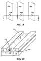
- FIGS. 1A through 1Fare cross sectional views showing a method of fabricating a dual damascene wire common to both a first and a second embodiment of the present invention
- FIG. 2Aa top view illustrating the section through which FIG. 1F is taken;
- FIG. 2Bis an isometric drawing of a trench and via opening as illustrated in FIG. 1F ;
- FIGS. 3A through 3Care cross sectional views of a method of fabricating a dual damascene wire according to the first embodiment of the present invention
- FIGS. 4A through 4Care cross sectional views of a method of fabricating a dual damascene wire according to the second embodiment of the present invention.
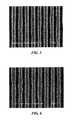
- FIGS. 5 and 6are SEM photomicrographs of imprinted structures formed from imprinting compositions according to embodiments of the present invention.
- the present inventionmay be advantageously used to fabricate damascene and dual-damascene wires and vias.
- the present inventioncombines imprint lithography with materials that can be converted to low dielectric constants (where k, the dielectric constant, is less than about 3.9) in order to fabricate damascene and dual-damascene interconnect structures for integrated circuits.
- Imprint lithographyis used with a photosensitive pre-dielectric material that is molded between a template having a relief pattern and a substrate, exposed to actinic radiation and the resulting patterned dielectric layer, having a three dimensional pattern, is used as part of a damascene or dual damascene process.
- a damascene processis one in which wire trenches or via openings are formed in a dielectric layer, an electrical conductor of sufficient thickness to fill the trenches is deposited on a top surface of the dielectric, and a chemical-mechanical-polish (CMP) process is performed to remove excess conductor and make the surface of the conductor co-planar with the surface of the dielectric layer to form damascene wires (or damascene vias).
- CMPchemical-mechanical-polish
- a dual-damascene processis one in which via openings are formed through the entire thickness of a dielectric layer followed by formation of trenches part of the way through the dielectric layer in any given cross-sectional view. All via openings are intersected by integral wire trenches above and by a wire trench below, but not all trenches need intersect a via opening.
- An electrical conductor of sufficient thickness to fill the trenches and via openingis deposited on a top surface of the dielectric, and a CMP process is performed to make the surface of the conductor in the trench co-planar with the surface of the dielectric layer to form dual-damascene wires and dual-damascene wires having integral dual-damascene vias.
- the present inventionwill be described in an exemplary dual damascene process, for forming wires with integral wires and vias, however it should be understood the method described is applicable to single damascene processes for forming wires or vias.
- FIGS. 1A through 1Fare cross sectional views showing a method of fabricating a dual damascene wire common to both a first and a second embodiment of the present invention.
- a substrate 100formed in a substrate 100 are electrically conductive wires (or contact studs) 105 .
- a top surface of wires 105is coplanar with a top surface of substrate 100 .
- copper diffusion barrier 110is silicon nitride.
- a dielectric precursor material 115is applied to the top surface of barrier 110 .
- Precursor dielectric material 115is a liquid.
- Dielectric precursor material 115includes one or more substituted polyhedral silsesquioxane (PSS) oligomers, a photoinitiator and/or a photo-acid generator.
- PSSpolyhedral silsesquioxane
- the substituent groups of the PSSare directly photo-polymerizable or polymerizable in the presence of a photoinitiator or photoacid generator.
- Dielectric precursor material 115advantageously has a low viscosity.
- the imprint materialfills the recesses in the template and also forms a so-called residual layer between the bottom-most surface of the template and the top-most surface of the substrate.
- a low viscosity imprint materialreduces the force and the time required to fill the template recesses and achieve an acceptably thin residual layer. Reducing the imprint force reduces mechanical distortions of the imprint template and allows for better alignment/overlay capabilities, while reducing the time to fill the template recesses and achieve an acceptably thin residual layer increases the throughput of the imprint process.
- substituted PSS oligomershave high viscosities it is advantageous to add low viscosity diluents to the dielectric precursor material.
- the substituted PSS oligomers of the embodiments of the present inventionhave viscosities of about 1000 centipoise or higher at about 20° C.
- the imprinted structuresee FIG. 1F
- dielectric precursor material 115may further include one or more low viscosity polymerizable diluents.
- one or all of the polymerizable diluentsare polymerizable monomers. In one example, the viscosity of one or all of the polymerizable diluents is less than about 30 centipoise at about 20° C. In one example, dielectric precursor material 115 includes about 50% by weight of polymerizable diluents. In one example, dielectric precursor material 115 includes about 50% by weight of polymerizable diluents having a viscosity of about 30 centipoise or less at about 20° C. In one example, dielectric precursor material 115 includes enough polymerizable diluents to reduce the viscosity of the precursor dielectric material to about 50 centipoise or less at about 20° C.
- precursor dielectric material 115has a viscosity of less than about 100 centipoise when measured at about 20° C.
- precursor dielectric material 115is a liquid which has a viscosity less than about 50 centipoise when measured at about 20° C.
- precursor dielectric material 115is a liquid which has a viscosity between about 20 centipoise and about 50 centipoise when measured at about 20° C.
- precursor dielectric material 115is a liquid which has a viscosity of about 20 centipoise or less when measured at about 20° C.
- composition of precursor dielectric material 115is described in detail infra.
- an imprint template 120includes a relief pattern made up of plateaus 125 and 130 rising above a reference surface 135 . Plateaus 130 rise above plateaus 125 .
- Imprint template 120is pressed with a low pressure (i.e., less than about 1 psi) toward substrate 100 , and the pool of dielectric precursor material 115 (see FIG. 1C ) is spread out over copper diffusion barrier 110 , completely filling the spaces between plateaus 125 and 130 and reference surface 135 and a top surface of copper diffusion barrier 110 .
- the dielectric precursor material 115(see FIG. 1C ) is converted (i.e. the PSS oligomers and polymerizable monomer are cross-linked) to a dielectric material 140 .
- actinic radiationin one example ultraviolet (UV) light
- the dielectric precursor material 115is converted (i.e. the PSS oligomers and polymerizable monomer are cross-linked) to a dielectric material 140 .
- template 120is removed exposing a top surface 145 of dielectric layer 140 and trenches 150 having integral pre-via openings 155 formed in the dielectric layer.
- Pre-via openings 155are open to top surface 145 of dielectric layer 140 .
- a residual layer 157 of dielectric material 115(see FIG. 1B ) remains in the bottom of pre-via openings 155 .
- a blanket etchis performed to remove any of residual layer 157 from the bottoms of via openings 155 (see FIG. 1E ) and an additional etch is performed to remove copper diffusion barrier 110 at the bottom of the vias opening and expose wires 105 .
- the blanket etchremoves a portion of top surface 145 (see FIG. 1E ) and creates a new top surface 145 A of dielectric layer 140 .
- Trench 150(see FIG. 1D ) is deepened to create trenches 150 A and vias 155 A are created.
- the blanket etch and the additional etchare reactive ion etches (RIEs).
- RIEsreactive ion etches
- a single RIE etchmay be performed to etch both dielectric layer 140 and copper diffusion barrier 110 .
- FIG. 2Aa top view illustrating the section through which FIG. 1F is taken.
- trenches 150 Aextend laterally and via openings 155 A are contained within the perimeter of trenches 150 A.
- the two opposite sides of via openings 155 A facing the sidewalls of the trenchmay extend to those sidewalls.
- FIG. 2Bis an isometric drawing of a trench and via opening as illustrated in FIG. 1F .
- via opening 155 Ais shown in cutaway and it is clear that trench 150 A is not as deep as via opening 155 A.
- FIGS. 3A through 3Care cross sectional views of a method of fabricating a dual damascene wire according to the first embodiment of the present invention.
- dielectric layer 140(see FIG. 1F ) is heated to a temperature high enough to fully cure the dielectric layer creating a porous dielectric layer 160 having pores 162 .
- the high temperature cureperforms three functions:
- the high temperature curedecomposes and volatize and drive out most if not all (if present) of the following carbonaceous materials: polymerized polymerizable monomers, non-polymerized polymerizable monomers, photoacid generators, photoacid generator reaction products, photoinitiators and photoinitiator reaction products thereby generating pores in the dielectric layer;
- the cureis performed at a temperature of at least about 300° C. In a second example, the cure is performed at a temperature between about 300° C. and about 400° C.
- porous dielectric layer 160has a dielectric constant of less than that of silicon dioxide. In a second example, porous dielectric layer 160 has a dielectric constant of less than about 3.9. In a third example, porous dielectric layer 160 has a dielectric constant of less than about 3.1. In a fourth example, porous dielectric layer 160 has a dielectric constant of less than about 2.9.
- non-thermal curemay be performed.
- non-thermal curesinclude but are not limited to exposure to ultra-violet radiation, microwave radiation and electron beams.
- a conformal electrically conductive layer 165is formed on all exposed surfaces of porous dielectric layer 160 and wires 105 and an electrically conductive layer 170 of sufficient thickness to overfill trenches 150 A (see FIG. 3A ) is formed on top of conductive layer 165 .
- conductive layer 165comprises tantalum, tantalum nitride, titanium, titanium nitride or combinations thereof.
- conductive layer 165comprises a seed layer of copper formed, for example, by deposition or evaporation.
- conductive layer 170comprises tungsten.
- conductive layer 170comprises copper formed, for example, by electroplating.
- a chemical-mechanical-polishis performed to form damascene wires 175 having integral via 180 , the vias in physical and electrical contact with wires 105 .
- Top surfaces 185 of wires 175are coplanar with a top surface 190 of porous dielectric layer 160 .
- FIGS. 4A through 4Care cross sectional views of a method of fabricating a dual damascene wire according to the second embodiment of the present invention.
- conformal electrically conductive layer 165is formed on all exposed surfaces of dielectric layer 140 and wires 105 .
- An electrically conductive layer 170 of sufficient thickness to overfill trenches 150 Ais formed on top of conductive layer 165 .
- the compositions of conductive layers 165 and 170have been described supra.
- a CMPis performed to form damascene wires 175 having integral vias 180 , contact with wires 105 exposed in the bottoms of the vias.
- Top surfaces 185 of wires 175are coplanar with a top surface 145 A of dielectric layer 140 .
- dielectric layer 140(see FIG. 4B ) is heated to a temperature high enough to fully cure the dielectric layer creating, a porous dielectric layer 160 having pores 162 .
- the curing processhas been described supra.
- the cureis performed at a temperature of at least 300° C. In a second example, the cure is performed at a temperature between about 300° C. and about 400° C.
- the properties of porous dielectric layer 160have been described supra.
- the imprintable precursor dielectric materials of the present inventioninclude one or more substituted PSS oligomers and a photoinitiator and/or a photo-acid generator.
- the precursor dielectric materialsmay further include a low viscosity polymerizable monomer and/or a solvent.
- One purpose for including a low viscosity polymerizable monomer and/or a solventis to reduce the viscosity of imprintable precursor dielectric materials.
- Another purpose for including a low viscosity polymerizable monomer and/or a solventis to provide additional porogen.
- the substituted PSS oligomers of the present inventionare resins having the structures (I), (II), (III) or (IV) where:
- T 8 Ris denoted by the formula T 8 R , where T represents R SiO 3/2 ;
- T 10 Ris denoted by the formula T 10 R , where T represents RSiO 3/2 ;
- T 12 Ris denoted by the formula T 12 R , where T represents R SiO 3/2 ;
- R groupsare independently selected from the group of polymerizable groups consisting of:
- the polymerizable R groupsmay comprises the structure—(L) n —P, where L is a linking group, n is 0 or 1 and P is a polymerizable moiety, wherein each linking group is independently selected from the group consisting of alkyl groups, cycloalkyl groups, siloxanes, alkylsilyl groups, and alkyl-siloxyl groups.
- the substituted PSS oligomers of the present inventionmay be denoted by the general formulas T m R where m is equal to 8, 10 or 12.
- T m Ra common name of the compound is octakis(N) silsesquioxane, where N is the name of the indicated R group.
- Structure (IV)may be considered exemplary of an open cage substituted PSS oligomer of a first type where each silicon atom of the cage is bound to the proper number of oxygen atoms (three in structure IV), while some of the oxygen atoms are not bound to two silicon atoms (the two —OH groups in structure IV).
- Structures (VI) and (VII) illustrated infraare examples of a second type of open cage PSS structure where one or more silicon atoms of the cage are not present, but every silicon atom of the cage is still bound to the proper number of oxygen atoms.
- Structures (I), (II) and (III)are closed cage substituted PSS oligomers.
- Structure (IV)is an open cage substituted T 8 PSS oligomer with two of the —Si—O—Si— cage bridges opened.
- Structures (VI) and VII)are open cage substituted T 8 PSS oligomers with one cage Si atom not present.
- the substituted PSS oligomersmay include open cage T 8 , T 10 and T 12 structures having one or more —Si—O—Si—O— bridges or one or more cage Si atoms not present.
- the imprinting formulations of the present inventionmay include mixtures of T 8 R PSS oligomers with different R groups.
- the imprinting formulations of the present inventionmay include mixtures of T 10 R PSS oligomers with different R groups.
- the imprinting formulations of the present inventionmay include mixtures of T 12 R PSS oligomers with different R groups.
- the imprinting formulations of the present inventionmay include mixtures of open and closed cage T 8 R , T 10 R and T 12 R PSS oligomers. The R groups need not be the same on different PSS oligomers of the imprinting formulations.
- Suitable photoinitiatorsinclude but are not limited to: acetophenone, anisoin, anthraquinone, anthraquinone-2-sulfonic acid, (benzene)tricarbonylchromium, benzil, benzoin, benzoin ethyl ether, benzoin isobutyl ether, benzoin methyl ether, benzophenone, 3,3′,4,4′-benzophenonetetracarboxylicdianhydride, 4-benzoylbiphenyl, 2-benzyl-2-(dimethylamino)-4′-morpholinobutyrophenone, 4,4′-bis(diethylamino)benzophenone, 4,4′-bis(dimethylamino)benzophenone, camphorquionone, 2-chlorothioxanthen-9-one, (cumene)cyclopentadienyliron(II)hexafluorophosphate, dibenzosuberenone,
- Suitable photo-acid generatorsinclude, but are not limited to: sulfonium salt, triphenylsulfonium perfluoromethanesulfonate (triphenylsulfonium triflate), triphenylsulfonium perfluorobutanesulfonate, triphenylsulfonium perfluoropentanesulfonate, triphenylsulfonium perfluorooctanesulfonate, triphenylsulfonium hexafluoroantimonate, triphenylsulfonium hexafluoroarsenate, triphenylsulfonium hexafluorophosphate, triphenylsulfonium bromide, triphenylsulfonium chloride, triphenylsulfonium iodide, 2,4,6-trimethylphenyldiphenylsulfonium perfluorobutanesulfonate, 2,4,
- T fCF 3 S(O) 2 O—.
- Suitable low viscosity polymerizable monomer diluentsinclude but are not limited to: mono- or di-functional methacrylates, including isobornyl methacrylate, glycidyl methacrylate, n-butyl methacrylate, methyl methacrylate and ethylene glycol dimethacrylate; methacrylate esters; mono- or di-functional acrylates including isobornyl acrylate, octyl acrylate, ethylene glycol diacrylate; vinyl ethers including butyl vinyl ether, ethylene glycol divinyl ether; and glycidyl ethers including ethylene glycol diglycidyl ether.
- the silsesquioxane starting materialoctakis(dimethylsilyloxy)silsesquioxane
- PSS derivative(Methacryloxypropyl)silsesquioxane cage mixture (8, 10 and 12 atom silicon cages) was also obtained from Hybrid Plastics.
- the photoinitiatorswere purchased from CIBA or Aldrich Chemical Company. All the other chemicals were purchased from Aldrich Chemical Company. The following examples are intended to provide those of ordinary skill in the art with a complete disclosure and description of how to prepare and use the compositions disclosed and claimed herein. Efforts have been made to ensure accuracy with respect to numbers (e.g., amounts, temperature, etc.), but allowance should be made for the possibility of errors and deviations.
- Dielectric constantswere determined using a capacitance bridge with an HP 4192A impedance analyzer using a metal insulator semi-conductor structure. Measurements were done at 25° C. and 100 KHz. Young's modulus measurements were obtained using a Fraunhofer LA Wave surface acoustic wave spectrometer (SAWS) operating between 50 MHz-200 MHz and sampling each specimen at five different spots. Densities were determined by specular x-ray reflectivity.
- SAWSFraunhofer LA Wave surface acoustic wave spectrometer
- Octakis(dimethylsilyloxy)silsesquioxane(10.2 grams, 0.01 mole), allyl methacrylate (10.10 g, 0.08 mole), and tetrahydrofuran (THF) (100 ml) were placed in a round bottom flask equipped with a magnetic stirrer, nitrogen inlet, and a water condenser. The flask was cooled in an ice/water bath and platinum(0)-1,3-divinyl-1,1,3,3-tetramethyldisiloxane complex in xylene (1 ml) was added to this mixture and stirred for one hour.
- THFtetrahydrofuran
- Imprinting composition 1is based on Octakis(methacryloxypropyl dimethylsilyloxy)silsesquioxane.
- the polymerizable substituent groupsare structure (V)A.
- Imprinting composition 1was formulated with octakis(methacryloxypropyl dimethylsilyloxy)silsesquioxane (1 g), DAROCUR 4265 (60 mg) and propylene glycol methyl ether acetate (PGMEA) (1.35 g).
- DAROCUR 4265is a mixture of 50% 2,4,6-trimethylbenzoyl-diphenyl-phosphineoxide and 50% 2-hydroxy-2-methyl-1-phenyl-propan-1-one.
- the resulting imprinting compositionwas filtered through a 0.2 micron filter. This imprinting composition was then spin coated on two 3 inch silicon wafers and both the films were exposed to 254 nm UV radiation for 5 minutes to polymerize the films. Afterwards, one of the two wafers was cured at 400° C. for 1 hour under N 2 atmosphere. TABLE I summarizes some properties of the thermally cured and uncured films. The thermally cured film has a dielectric constant of 2.89.
- Imprinting composition 2is based on a (Methacryloxypropyl)silsesquioxane mixture.
- the polymerizable substituent groupsare structure (V)B the PSS base structures were closed cage T 8 , T 10 and T 12 .
- Imprinting composition 2was formulated with the (Methacryloxypropyl)silsesquioxane cage mixture (1.0 gram), IRGACURE 184 (1-hydroxycyclohexyl phenyl ketone) (30 mg), IRGACURE 819 (diphenyl(2,4,6-trimethylbenzoyl)phosphine oxide) and propylene glycol methyl ether acetate (PGMEA) (structure 3F) (2.0 g) were added. The resulting imprinting composition was filtered through a 0.2 micron filter. The imprinting composition was then spin coated on two 3 inch silicon wafers and both the films were exposed to 365 nm radiation for 15 minutes to polymerize the films. Afterwards, one of the two wafers was cured at 400° C. for 1 hour under N 2 atmosphere. TABLE II summarizes some properties of the thermally cured and uncured films. The thermally cured film has a dielectric constant of 3.05.
- Imprinting composition 3is based on Octakis(methacryloxypropyl dimethylsilyloxy)silsesquioxane.
- the polymerizable substituent groupsare structure (V)A and the polymerizable diluent isobornyl methacrylate.
- Imprinting compositionwas formulated with octakis(methacryloxypropyl dimethylsilyloxy)silsesquioxane (2.0 g), isobornyl methacrylate (4.0 g), and IRGACURE 184 (150 mg) and IRGACURE 819 (150 mg). The resulting formulation was filtered through a 0.2 micron filter. The viscosity of the formulation is 25 cPs at 20° C. Imprints of this formulation were obtained using a MII55 imprint tool. A top down SEM of nominal 50 nm line/space features obtained are illustrated in FIG. 5 .
- Imprinting composition 4is based on a (Methacryloxypropyl)silsesquioxane mixture.
- the polymerizable substituent groupsare structure (V)B the PSS base structures were closed cage T 8 , T 10 and T 12 and the polymerizable diluent is isobornyl methacrylate.
- Imprintable composition 4was formulated with the Methacryloxypropyl silsesquioxane cage mixture (1 g), isobornyl methacrylate (1 g), and IRGACURE 184 (60 mg) and IRGACURE 819 (60 mg). The resulting formulation was filtered through a 0.2 micron filter. The viscosity of this formulation is 80 centipoise at 20° C. The imprints of this formulation were obtained using a MII55 imprint tool. A top down SEM of nominal 50 nm line/space features obtained are illustrated in FIG. 6 .
- the embodiments of the present inventionprovide semiconductor interconnection structures and processes that are dense and have low capacitance.
Landscapes
- Engineering & Computer Science (AREA)
- Physics & Mathematics (AREA)
- Condensed Matter Physics & Semiconductors (AREA)
- General Physics & Mathematics (AREA)
- Manufacturing & Machinery (AREA)
- Computer Hardware Design (AREA)
- Microelectronics & Electronic Packaging (AREA)
- Power Engineering (AREA)
- Chemical & Material Sciences (AREA)
- Materials Engineering (AREA)
- Chemical Kinetics & Catalysis (AREA)
- Life Sciences & Earth Sciences (AREA)
- Wood Science & Technology (AREA)
- Organic Chemistry (AREA)
- Plasma & Fusion (AREA)
- Internal Circuitry In Semiconductor Integrated Circuit Devices (AREA)
- Macromonomer-Based Addition Polymer (AREA)
Abstract
Description


wherein one or more R groups are independently selected from the group of polymerizable groups consisting of:


| TABLE I | ||||||
| Water | ||||||
| Thickness | Refractive | Contact | Density | Dielectric | E Modulus | |
| FILM | (nm) | Index | Angle | (gram/cm3) | Constant | (GPa) |
| NOT CURED | 866 | 1.4825 | 90° | 1.24 | 3.98 | 7.03 +− 0.13 |
| CURED 400° C. | 559 | 1.4082 | 92° | 1.17 | 2.89 | 3.55 +− 0.07 |
| TABLE II | ||||||
| Water | ||||||
| Thickness | Refractive | Contact | Density | Dielectric | E Modulus | |
| FILM | (nm) | Index | Angle | (gram/cm3) | Constant | (GPa) |
| NOT CURED | 1075 | 1.49015 | 75° | 1.348 | 4.36 | 6.29 +− 0.12 |
| CURED 400° C. | 664 | 1.4811 | 72° | 1.268 | 3.05 | 5.97 +− 0.10 |
Claims (1)
Priority Applications (3)
| Application Number | Priority Date | Filing Date | Title |
|---|---|---|---|
| US11/398,135US7468330B2 (en) | 2006-04-05 | 2006-04-05 | Imprint process using polyhedral oligomeric silsesquioxane based imprint materials |
| US12/053,893US8026293B2 (en) | 2006-04-05 | 2008-03-24 | Polyhedral oligomeric silsesquioxane based imprint materials and imprint process using polyhedral oligomeric silsesquioxane based imprint materials |
| US13/170,221US8603584B2 (en) | 2006-04-05 | 2011-06-28 | Polyhedral oligomeric silsesquioxane based imprint materials and imprint process using polyhedral oligomeric silsesquioxane based imprint materials |
Applications Claiming Priority (1)
| Application Number | Priority Date | Filing Date | Title |
|---|---|---|---|
| US11/398,135US7468330B2 (en) | 2006-04-05 | 2006-04-05 | Imprint process using polyhedral oligomeric silsesquioxane based imprint materials |
Related Child Applications (1)
| Application Number | Title | Priority Date | Filing Date |
|---|---|---|---|
| US12/053,893ContinuationUS8026293B2 (en) | 2006-04-05 | 2008-03-24 | Polyhedral oligomeric silsesquioxane based imprint materials and imprint process using polyhedral oligomeric silsesquioxane based imprint materials |
Publications (2)
| Publication Number | Publication Date |
|---|---|
| US20070238317A1 US20070238317A1 (en) | 2007-10-11 |
| US7468330B2true US7468330B2 (en) | 2008-12-23 |
Family
ID=38575886
Family Applications (3)
| Application Number | Title | Priority Date | Filing Date |
|---|---|---|---|
| US11/398,135Expired - Fee RelatedUS7468330B2 (en) | 2006-04-05 | 2006-04-05 | Imprint process using polyhedral oligomeric silsesquioxane based imprint materials |
| US12/053,893Expired - Fee RelatedUS8026293B2 (en) | 2006-04-05 | 2008-03-24 | Polyhedral oligomeric silsesquioxane based imprint materials and imprint process using polyhedral oligomeric silsesquioxane based imprint materials |
| US13/170,221Expired - Fee RelatedUS8603584B2 (en) | 2006-04-05 | 2011-06-28 | Polyhedral oligomeric silsesquioxane based imprint materials and imprint process using polyhedral oligomeric silsesquioxane based imprint materials |
Family Applications After (2)
| Application Number | Title | Priority Date | Filing Date |
|---|---|---|---|
| US12/053,893Expired - Fee RelatedUS8026293B2 (en) | 2006-04-05 | 2008-03-24 | Polyhedral oligomeric silsesquioxane based imprint materials and imprint process using polyhedral oligomeric silsesquioxane based imprint materials |
| US13/170,221Expired - Fee RelatedUS8603584B2 (en) | 2006-04-05 | 2011-06-28 | Polyhedral oligomeric silsesquioxane based imprint materials and imprint process using polyhedral oligomeric silsesquioxane based imprint materials |
Country Status (1)
| Country | Link |
|---|---|
| US (3) | US7468330B2 (en) |
Cited By (11)
| Publication number | Priority date | Publication date | Assignee | Title |
|---|---|---|---|---|
| US20060261518A1 (en)* | 2005-02-28 | 2006-11-23 | Board Of Regents, The University Of Texas System | Use of step and flash imprint lithography for direct imprinting of dielectric materials for dual damascene processing |
| US20080003818A1 (en)* | 2006-06-30 | 2008-01-03 | Robert Seidel | Nano imprint technique with increased flexibility with respect to alignment and feature shaping |
| US20080118995A1 (en)* | 2006-11-17 | 2008-05-22 | Dnyanesh Chandrakant Tamboli | Method and composition for restoring dielectric properties of porous dielectric materials |
| US20110079579A1 (en)* | 2009-10-06 | 2011-04-07 | International Business Machines Corporation | Planarization over topography with molecular glass materials |
| US20110083887A1 (en)* | 2009-10-08 | 2011-04-14 | International Business Machines Corporation | Photo-patternable dielectric materials curable to porous dielectric materials, formulations, precursors and methods of use thereof |
| US20110256713A1 (en)* | 2006-04-05 | 2011-10-20 | International Business Machines Corporation | Polyhedral oligomeric silsesquioxane based imprint materials and imprint process using polyhedral oligomeric silsesquioxane based imprint materials |
| US8460256B2 (en) | 2009-07-15 | 2013-06-11 | Allegiance Corporation | Collapsible fluid collection and disposal system and related methods |
| US8500706B2 (en) | 2007-03-23 | 2013-08-06 | Allegiance Corporation | Fluid collection and disposal system having interchangeable collection and other features and methods relating thereto |
| US8513321B2 (en) | 2010-11-05 | 2013-08-20 | Ppg Industries Ohio, Inc. | Dual cure coating compositions, methods of coating a substrate, and related coated substrates |
| US9889239B2 (en) | 2007-03-23 | 2018-02-13 | Allegiance Corporation | Fluid collection and disposal system and related methods |
| WO2018169538A1 (en)* | 2017-03-16 | 2018-09-20 | Intel Corporation | Photoresist with electron-activated photosensitizers for confined patterning lithography |
Families Citing this family (23)
| Publication number | Priority date | Publication date | Assignee | Title |
|---|---|---|---|---|
| CN101883797B (en)* | 2007-11-30 | 2012-10-17 | 昭和电工株式会社 | Curable composition for transfer material and fine pattern forming method using same |
| JP5611519B2 (en)* | 2008-10-29 | 2014-10-22 | 富士フイルム株式会社 | Composition for nanoimprint, pattern and method for forming the same |
| US8431670B2 (en) | 2009-08-31 | 2013-04-30 | International Business Machines Corporation | Photo-patternable dielectric materials and formulations and methods of use |
| WO2011059967A2 (en)* | 2009-11-10 | 2011-05-19 | Georgia Tech Research Corporation | Polyhedral oligomeric silsesquioxane compositions, methods of using these compositions, and structures including these compositions |
| US8353410B2 (en)* | 2009-11-24 | 2013-01-15 | International Business Machines Corporation | Polymeric films made from polyhedral oligomeric silsesquioxane (POSS) and a hydrophilic comonomer |
| US8011517B2 (en)* | 2009-11-24 | 2011-09-06 | International Business Machines Corporation | Composite membranes with performance enhancing layers |
| KR101158462B1 (en)* | 2010-03-11 | 2012-06-19 | (주)화인졸 | UV curable resin composition of organic-inorganic hybride type |
| KR101248530B1 (en) | 2010-09-17 | 2013-04-03 | 한국과학기술연구원 | A Composition Comprising a Monomer for Polymerizing Branch-type Silsesquioxane Polymer, Branch-type Silsesquioxane Polymer Synthesized from the Same and A Method for Synthesizing the Same |
| WO2012119615A1 (en)* | 2011-03-09 | 2012-09-13 | Johannes Kepler Universität Linz | Silsesquioxane polymers |
| US8895104B2 (en) | 2011-07-01 | 2014-11-25 | International Business Machines Corporation | Thin film composite membranes embedded with molecular cage compounds |
| JP6012344B2 (en)* | 2011-10-24 | 2016-10-25 | キヤノン株式会社 | Method for forming film |
| JP6011230B2 (en)* | 2011-10-25 | 2016-10-19 | セントラル硝子株式会社 | Siloxane composition, cured product thereof and use thereof |
| US9428605B2 (en)* | 2012-11-08 | 2016-08-30 | Neo Sitech Llc | Organic-inorganic hybrid material compositions and polymer composites |
| US8999625B2 (en) | 2013-02-14 | 2015-04-07 | International Business Machines Corporation | Silicon-containing antireflective coatings including non-polymeric silsesquioxanes |
| CN104869762A (en)* | 2014-02-24 | 2015-08-26 | 联想(北京)有限公司 | Preparation method and structure of PCB and electronic equipment |
| CN104703408B (en)* | 2015-03-10 | 2018-05-15 | 上海量子绘景电子股份有限公司 | The preparation method of high density copper coating board |
| KR102242545B1 (en)* | 2017-09-27 | 2021-04-19 | 주식회사 엘지화학 | Antibacterial polymer coating composition and antibacterial polymer film |
| WO2019193457A1 (en)* | 2018-04-02 | 2019-10-10 | 3M Innovative Properties Company | Electrical device having jumper |
| SG11202012635YA (en)* | 2018-07-20 | 2021-01-28 | Illumina Inc | Resin composition and flow cells incorporating the same |
| CN109233294B (en)* | 2018-08-28 | 2020-04-24 | 淮阴工学院 | Organic silicon micro-porous ultralow dielectric film and preparation method thereof |
| US11281094B2 (en)* | 2018-11-15 | 2022-03-22 | Applied Materials, Inc. | Method for via formation by micro-imprinting |
| TW202130416A (en)* | 2019-12-20 | 2021-08-16 | 美商伊路米納有限公司 | Flow cells |
| CN113881048B (en)* | 2021-11-11 | 2023-02-28 | 陇东学院 | Trifunctional vinyl POSS (polyhedral oligomeric silsesquioxane) as well as preparation method and application thereof |
Citations (11)
| Publication number | Priority date | Publication date | Assignee | Title |
|---|---|---|---|---|
| US5484867A (en)* | 1993-08-12 | 1996-01-16 | The University Of Dayton | Process for preparation of polyhedral oligomeric silsesquioxanes and systhesis of polymers containing polyhedral oligomeric silsesqioxane group segments |
| US5861235A (en) | 1996-06-26 | 1999-01-19 | Dow Corning Asia, Ltd. | Ultraviolet-curable composition and method for patterning the cured product therefrom |
| US5949130A (en) | 1997-09-17 | 1999-09-07 | Fujitsu Limited | Semiconductor integrated circuit device employing interlayer insulating film with low dielectric constant |
| US20020192980A1 (en) | 2001-06-19 | 2002-12-19 | Hogle Richard A. | Methods for forming low-k dielectric films |
| US6576345B1 (en) | 2000-11-30 | 2003-06-10 | Novellus Systems Inc | Dielectric films with low dielectric constants |
| US6730617B2 (en) | 2002-04-24 | 2004-05-04 | Ibm | Method of fabricating one or more tiers of an integrated circuit |
| US20040137241A1 (en) | 2003-01-08 | 2004-07-15 | International Business Machines Corporation | Patternable low dielectric constsnt materials and their use in ULSI interconnection |
| US20050031964A1 (en) | 2003-08-05 | 2005-02-10 | International Business Machines Corporation | Lithographic antireflective hardmask compositions and uses thereof |
| US6873026B1 (en) | 2002-03-04 | 2005-03-29 | Novellus Systems, Inc. | Inhomogeneous materials having physical properties decoupled from desired functions |
| WO2005031855A1 (en) | 2003-09-29 | 2005-04-07 | International Business Machines Corporation | Fabrication method |
| US20050202350A1 (en) | 2004-03-13 | 2005-09-15 | Colburn Matthew E. | Method for fabricating dual damascene structures using photo-imprint lithography, methods for fabricating imprint lithography molds for dual damascene structures, materials for imprintable dielectrics and equipment for photo-imprint lithography used in dual damascene patterning |
Family Cites Families (4)
| Publication number | Priority date | Publication date | Assignee | Title |
|---|---|---|---|---|
| US7008749B2 (en)* | 2001-03-12 | 2006-03-07 | The University Of North Carolina At Charlotte | High resolution resists for next generation lithographies |
| TW200413417A (en)* | 2002-10-31 | 2004-08-01 | Arch Spec Chem Inc | Novel copolymer, photoresist compositions thereof and deep UV bilayer system thereof |
| US7691275B2 (en)* | 2005-02-28 | 2010-04-06 | Board Of Regents, The University Of Texas System | Use of step and flash imprint lithography for direct imprinting of dielectric materials for dual damascene processing |
| US7468330B2 (en) | 2006-04-05 | 2008-12-23 | International Business Machines Corporation | Imprint process using polyhedral oligomeric silsesquioxane based imprint materials |
- 2006
- 2006-04-05USUS11/398,135patent/US7468330B2/ennot_activeExpired - Fee Related
- 2008
- 2008-03-24USUS12/053,893patent/US8026293B2/ennot_activeExpired - Fee Related
- 2011
- 2011-06-28USUS13/170,221patent/US8603584B2/ennot_activeExpired - Fee Related
Patent Citations (11)
| Publication number | Priority date | Publication date | Assignee | Title |
|---|---|---|---|---|
| US5484867A (en)* | 1993-08-12 | 1996-01-16 | The University Of Dayton | Process for preparation of polyhedral oligomeric silsesquioxanes and systhesis of polymers containing polyhedral oligomeric silsesqioxane group segments |
| US5861235A (en) | 1996-06-26 | 1999-01-19 | Dow Corning Asia, Ltd. | Ultraviolet-curable composition and method for patterning the cured product therefrom |
| US5949130A (en) | 1997-09-17 | 1999-09-07 | Fujitsu Limited | Semiconductor integrated circuit device employing interlayer insulating film with low dielectric constant |
| US6576345B1 (en) | 2000-11-30 | 2003-06-10 | Novellus Systems Inc | Dielectric films with low dielectric constants |
| US20020192980A1 (en) | 2001-06-19 | 2002-12-19 | Hogle Richard A. | Methods for forming low-k dielectric films |
| US6873026B1 (en) | 2002-03-04 | 2005-03-29 | Novellus Systems, Inc. | Inhomogeneous materials having physical properties decoupled from desired functions |
| US6730617B2 (en) | 2002-04-24 | 2004-05-04 | Ibm | Method of fabricating one or more tiers of an integrated circuit |
| US20040137241A1 (en) | 2003-01-08 | 2004-07-15 | International Business Machines Corporation | Patternable low dielectric constsnt materials and their use in ULSI interconnection |
| US20050031964A1 (en) | 2003-08-05 | 2005-02-10 | International Business Machines Corporation | Lithographic antireflective hardmask compositions and uses thereof |
| WO2005031855A1 (en) | 2003-09-29 | 2005-04-07 | International Business Machines Corporation | Fabrication method |
| US20050202350A1 (en) | 2004-03-13 | 2005-09-15 | Colburn Matthew E. | Method for fabricating dual damascene structures using photo-imprint lithography, methods for fabricating imprint lithography molds for dual damascene structures, materials for imprintable dielectrics and equipment for photo-imprint lithography used in dual damascene patterning |
Cited By (23)
| Publication number | Priority date | Publication date | Assignee | Title |
|---|---|---|---|---|
| US7691275B2 (en)* | 2005-02-28 | 2010-04-06 | Board Of Regents, The University Of Texas System | Use of step and flash imprint lithography for direct imprinting of dielectric materials for dual damascene processing |
| US20060261518A1 (en)* | 2005-02-28 | 2006-11-23 | Board Of Regents, The University Of Texas System | Use of step and flash imprint lithography for direct imprinting of dielectric materials for dual damascene processing |
| US20110256713A1 (en)* | 2006-04-05 | 2011-10-20 | International Business Machines Corporation | Polyhedral oligomeric silsesquioxane based imprint materials and imprint process using polyhedral oligomeric silsesquioxane based imprint materials |
| US8603584B2 (en)* | 2006-04-05 | 2013-12-10 | International Business Machines Corporation | Polyhedral oligomeric silsesquioxane based imprint materials and imprint process using polyhedral oligomeric silsesquioxane based imprint materials |
| US20080003818A1 (en)* | 2006-06-30 | 2008-01-03 | Robert Seidel | Nano imprint technique with increased flexibility with respect to alignment and feature shaping |
| US7928004B2 (en)* | 2006-06-30 | 2011-04-19 | Advanced Micro Devices, Inc. | Nano imprint technique with increased flexibility with respect to alignment and feature shaping |
| US20080118995A1 (en)* | 2006-11-17 | 2008-05-22 | Dnyanesh Chandrakant Tamboli | Method and composition for restoring dielectric properties of porous dielectric materials |
| US7977121B2 (en)* | 2006-11-17 | 2011-07-12 | Air Products And Chemicals, Inc. | Method and composition for restoring dielectric properties of porous dielectric materials |
| US8500706B2 (en) | 2007-03-23 | 2013-08-06 | Allegiance Corporation | Fluid collection and disposal system having interchangeable collection and other features and methods relating thereto |
| US10252856B2 (en) | 2007-03-23 | 2019-04-09 | Allegiance Corporation | Fluid collection and disposal system having interchangeable collection and other features and methods relating thereof |
| US9889239B2 (en) | 2007-03-23 | 2018-02-13 | Allegiance Corporation | Fluid collection and disposal system and related methods |
| US9604778B2 (en) | 2007-03-23 | 2017-03-28 | Allegiance Corporation | Fluid collection and disposal system having interchangeable collection and other features and methods relating thereto |
| US8460256B2 (en) | 2009-07-15 | 2013-06-11 | Allegiance Corporation | Collapsible fluid collection and disposal system and related methods |
| US8377631B2 (en) | 2009-10-06 | 2013-02-19 | International Business Machines Corporation | Planarization over topography with molecular glass materials |
| US9235124B2 (en) | 2009-10-06 | 2016-01-12 | Globalfoundries Inc. | Planarization over topography with molecular glass materials |
| US20110079579A1 (en)* | 2009-10-06 | 2011-04-07 | International Business Machines Corporation | Planarization over topography with molecular glass materials |
| US8389663B2 (en) | 2009-10-08 | 2013-03-05 | International Business Machines Corporation | Photo-patternable dielectric materials curable to porous dielectric materials, formulations, precursors and methods of use thereof |
| US9006373B2 (en) | 2009-10-08 | 2015-04-14 | International Business Machines Corporation | Photo-patternable dielectric materials curable to porous dielectric materials, formulations, precursors and methods of use thereof |
| US8981031B2 (en) | 2009-10-08 | 2015-03-17 | International Business Machines Corporation | Photo-patternable dielectric materials curable to porous dielectric materials, formulations, precursors and methods of use thereof |
| US8946371B2 (en) | 2009-10-08 | 2015-02-03 | International Business Machines Corporation | Photo-patternable dielectric materials curable to porous dielectric materials, formulations, precursors and methods of use thereof |
| US20110083887A1 (en)* | 2009-10-08 | 2011-04-14 | International Business Machines Corporation | Photo-patternable dielectric materials curable to porous dielectric materials, formulations, precursors and methods of use thereof |
| US8513321B2 (en) | 2010-11-05 | 2013-08-20 | Ppg Industries Ohio, Inc. | Dual cure coating compositions, methods of coating a substrate, and related coated substrates |
| WO2018169538A1 (en)* | 2017-03-16 | 2018-09-20 | Intel Corporation | Photoresist with electron-activated photosensitizers for confined patterning lithography |
Also Published As
| Publication number | Publication date |
|---|---|
| US20110256713A1 (en) | 2011-10-20 |
| US20080166871A1 (en) | 2008-07-10 |
| US8603584B2 (en) | 2013-12-10 |
| US8026293B2 (en) | 2011-09-27 |
| US20070238317A1 (en) | 2007-10-11 |
Similar Documents
| Publication | Publication Date | Title |
|---|---|---|
| US7468330B2 (en) | Imprint process using polyhedral oligomeric silsesquioxane based imprint materials | |
| US8617786B2 (en) | Poly-oxycarbosilane compositions for use in imprint lithography | |
| US8389663B2 (en) | Photo-patternable dielectric materials curable to porous dielectric materials, formulations, precursors and methods of use thereof | |
| US8461039B2 (en) | Patternable low-K dielectric interconnect structure with a graded cap layer and method of fabrication | |
| US7709370B2 (en) | Spin-on antireflective coating for integration of patternable dielectric materials and interconnect structures | |
| US8659115B2 (en) | Airgap-containing interconnect structure with improved patternable low-K material and method of fabricating | |
| US8952539B2 (en) | Methods for fabrication of an air gap-containing interconnect structure | |
| US8618663B2 (en) | Patternable dielectric film structure with improved lithography and method of fabricating same | |
| US9012587B2 (en) | Photo-patternable dielectric materials and formulations and methods of use | |
| US8896120B2 (en) | Structures and methods for air gap integration | |
| JP5636277B2 (en) | Porous insulating film and method for producing the same | |
| US20110042790A1 (en) | MULTIPLE PATTERNING USING IMPROVED PATTERNABLE LOW-k DIELECTRIC MATERIALS |
Legal Events
| Date | Code | Title | Description |
|---|---|---|---|
| AS | Assignment | Owner name:INTERNATIONAL BUSINESS MACHINES CORPORATION, NEW Y Free format text:ASSIGNMENT OF ASSIGNORS INTEREST;ASSIGNORS:ALLEN, ROBERT DAVID;DIPIETRO, RICHARD ANTHONY;DUBOIS, GERAUD JEAN-MICHEL;AND OTHERS;REEL/FRAME:017762/0520;SIGNING DATES FROM 20060317 TO 20060405 | |
| FEPP | Fee payment procedure | Free format text:PAYOR NUMBER ASSIGNED (ORIGINAL EVENT CODE: ASPN); ENTITY STATUS OF PATENT OWNER: LARGE ENTITY | |
| STCF | Information on status: patent grant | Free format text:PATENTED CASE | |
| REMI | Maintenance fee reminder mailed | ||
| FPAY | Fee payment | Year of fee payment:4 | |
| SULP | Surcharge for late payment | ||
| AS | Assignment | Owner name:GLOBALFOUNDRIES U.S. 2 LLC, NEW YORK Free format text:ASSIGNMENT OF ASSIGNORS INTEREST;ASSIGNOR:INTERNATIONAL BUSINESS MACHINES CORPORATION;REEL/FRAME:036550/0001 Effective date:20150629 | |
| AS | Assignment | Owner name:GLOBALFOUNDRIES INC., CAYMAN ISLANDS Free format text:ASSIGNMENT OF ASSIGNORS INTEREST;ASSIGNORS:GLOBALFOUNDRIES U.S. 2 LLC;GLOBALFOUNDRIES U.S. INC.;REEL/FRAME:036779/0001 Effective date:20150910 | |
| FPAY | Fee payment | Year of fee payment:8 | |
| AS | Assignment | Owner name:WILMINGTON TRUST, NATIONAL ASSOCIATION, DELAWARE Free format text:SECURITY AGREEMENT;ASSIGNOR:GLOBALFOUNDRIES INC.;REEL/FRAME:049490/0001 Effective date:20181127 | |
| FEPP | Fee payment procedure | Free format text:MAINTENANCE FEE REMINDER MAILED (ORIGINAL EVENT CODE: REM.); ENTITY STATUS OF PATENT OWNER: LARGE ENTITY | |
| AS | Assignment | Owner name:GLOBALFOUNDRIES INC., CAYMAN ISLANDS Free format text:RELEASE BY SECURED PARTY;ASSIGNOR:WILMINGTON TRUST, NATIONAL ASSOCIATION;REEL/FRAME:054636/0001 Effective date:20201117 | |
| LAPS | Lapse for failure to pay maintenance fees | Free format text:PATENT EXPIRED FOR FAILURE TO PAY MAINTENANCE FEES (ORIGINAL EVENT CODE: EXP.); ENTITY STATUS OF PATENT OWNER: LARGE ENTITY | |
| STCH | Information on status: patent discontinuation | Free format text:PATENT EXPIRED DUE TO NONPAYMENT OF MAINTENANCE FEES UNDER 37 CFR 1.362 | |
| FP | Lapsed due to failure to pay maintenance fee | Effective date:20201223 | |
| AS | Assignment | Owner name:GLOBALFOUNDRIES U.S. INC., NEW YORK Free format text:RELEASE BY SECURED PARTY;ASSIGNOR:WILMINGTON TRUST, NATIONAL ASSOCIATION;REEL/FRAME:056987/0001 Effective date:20201117 |