US7466594B2 - Dynamic matching of signal path and reference path for sensing - Google Patents
Dynamic matching of signal path and reference path for sensingDownload PDFInfo
- Publication number
- US7466594B2 US7466594B2US11/490,539US49053906AUS7466594B2US 7466594 B2US7466594 B2US 7466594B2US 49053906 AUS49053906 AUS 49053906AUS 7466594 B2US7466594 B2US 7466594B2
- Authority
- US
- United States
- Prior art keywords
- bit line
- cell
- global bit
- cells
- array
- Prior art date
- Legal status (The legal status is an assumption and is not a legal conclusion. Google has not performed a legal analysis and makes no representation as to the accuracy of the status listed.)
- Expired - Lifetime, expires
Links
- 230000015654memoryEffects0.000claimsabstractdescription56
- 238000000034methodMethods0.000claimsabstractdescription16
- 230000008878couplingEffects0.000claimsdescription6
- 238000010168coupling processMethods0.000claimsdescription6
- 238000005859coupling reactionMethods0.000claimsdescription6
- 230000009977dual effectEffects0.000claimsdescription3
- 230000003213activating effectEffects0.000description10
- 238000010586diagramMethods0.000description2
- 238000009792diffusion processMethods0.000description2
- 238000002955isolationMethods0.000description2
- 230000009467reductionEffects0.000description2
- 238000003491arrayMethods0.000description1
- 230000000903blocking effectEffects0.000description1
- 230000004048modificationEffects0.000description1
- 238000012986modificationMethods0.000description1
- 238000005192partitionMethods0.000description1
- 230000004044responseEffects0.000description1
- 230000011218segmentationEffects0.000description1
- 230000006641stabilisationEffects0.000description1
- 238000011105stabilizationMethods0.000description1
Images


Classifications
- G—PHYSICS
- G11—INFORMATION STORAGE
- G11C—STATIC STORES
- G11C16/00—Erasable programmable read-only memories
- G11C16/02—Erasable programmable read-only memories electrically programmable
- G11C16/06—Auxiliary circuits, e.g. for writing into memory
- G11C16/26—Sensing or reading circuits; Data output circuits
- G11C16/28—Sensing or reading circuits; Data output circuits using differential sensing or reference cells, e.g. dummy cells
- G—PHYSICS
- G11—INFORMATION STORAGE
- G11C—STATIC STORES
- G11C7/00—Arrangements for writing information into, or reading information out from, a digital store
- G11C7/14—Dummy cell management; Sense reference voltage generators
- G—PHYSICS
- G11—INFORMATION STORAGE
- G11C—STATIC STORES
- G11C16/00—Erasable programmable read-only memories
- G11C16/02—Erasable programmable read-only memories electrically programmable
- G11C16/04—Erasable programmable read-only memories electrically programmable using variable threshold transistors, e.g. FAMOS
- G11C16/0491—Virtual ground arrays
Definitions
- the present inventiongenerally relates to AC sensing schemes used for memory systems, such as flash memories, and particularly to a method for dynamic matching of the reference signal path and the sensed cell path without any area penalty, by using a non-accessed path in the array.
- Reading the contents of memory cellsgenerally involves sensing the current or voltage of the cell.
- Many kinds of sensing schemesare known in the art for memory cell arrays, such as flash or other non-volatile memories.
- One type of sensing schemeinvolves comparing the sensed cell to a reference cell.
- FIG. 1illustrates a prior art example of an AC matching scheme between an array sensed cell and a reference cell.
- a bit line (BL) driver 24drives the drain side of the sensed cell 12 .
- the BL driver 24is connected to the sensed cell 12 via a YMUX (Y multiplexer) 26 , via a driving path that includes one of the GBLs 18 , one of the select transistors 20 and one of the local bit lines 16 , which, in this case, serves as a drain diffusion bit-line (DBL).
- the connecting line to which the select transistor 20 is connectedis referred to as select line 14 (designated as select line SEL [ 8 : 0 ] in FIG. 1 ), and the connecting line in the YMUX 26 is referred to as the BS line.
- a sense amplifier 28senses the source side of the sensed cell 12 .
- the path from the source of the sensed cell 12 to the sense amplifier 28is through one of the local bit lines 16 , which, in this case, serves as a source diffusion bit-line, one of the select transistors 20 , one of the GBLs 18 and the YMUx 26 .
- a reference cell 30is used for the sense amplifier 28 .
- the reference cell 30is located in a reference mini-array 32 .
- a matched reference BL (REF-BL) driver 34is used in conjunction with a reference YMUX (REF-YMUX) 36 , reference select transistors 38 (also referred to as ref-select transistors) and matched reference DBLs (REF-DBL) 40 . Since most of the capacitance of the array cell path is the GBL capacitance (due to both to GND and coupling capacitance), reference GBLs (REF-GBLs) 42 are used to load the source side and the drain side of the reference path.
- the connecting line to which the ref-select transistor 38 is connectedis referred to as the REF_SEL line, and the connecting line in the YMUX. 36 is referred to as the REF_BS line.
- U.S. Pat. No. 6,535,434describes an architecture and method for implementing a non-strobed operation on an array cell, in which a reference unit is provided for emulating the response of the array cell during a desired operation (e.g., read, program verify, erase verify or other types of read operations).
- a desired operatione.g., read, program verify, erase verify or other types of read operations.
- the architecture and methodpermit relatively noise-free array cell interrogations at close to ground voltage levels.
- the read operationis performed by means of selecting the appropriate BS and SEL lines connecting the drain side of the array cell 12 to the BL driver 24 (at node BL_D) and by means of enabling the appropriate BS and SEL lines connecting the source side of the array cell 12 to the sense amplifier 28 (at node BL_S).
- the same procedureis applied for the reference cell 30 , i.e. enabling the appropriate REF_SEL and REF_BS lines to supply drain voltage from the REF_BL driver 34 (at node REF_BL_D) and connecting the source side of the reference cell 30 to the sense amplifier 28 (at node BL_REF).
- SAsense amplifier
- FIG. 2illustrates the signals generated at the inputs of the SA 28 with a 1C:1C load capacitance ratio matching scheme.
- “1C:1C load capacitance ratio matching”means that the capacitance for the sensed cell path and the capacitance for the reference signal path are fully matched.
- Time T 1represents the time of stabilization of the different nodes.
- the signals BL_S and BL_REFare generated respectively by the array cell 12 and the reference cell 30 charging the total path capacitance. The difference between the signals BL_S and BL_REF depends only on the different programming level of the cells 12 and 30 .
- the reference cell 30is programmed so that its current level would be between a programmed array cell and an erased array cell.
- a decision circuitis used for providing logical output describing the analog output of the SA 28 .
- the matching between the reference path and the sensed cell pathis maintained by copying the sensed cell path to the reference path.
- Thishas the disadvantage of multiplying the power dissipation during the sensing period and has a large area penalty.
- the area penaltyis two GBLs 18 per sense amplifier 28 and the power penalty is due to the need to drive two drain side GBLs for each read sequence.
- present inventionseeks to provide AC sensing schemes used for memory systems such as but not limited to, flash memories.
- present inventionseeks to provide dynamic matching of the reference signal path and the sensed cell path without any area penalty, by using a non-accessed path in the array. For example, instead of using designated REF_GBLs for the matching, an unused GBL from the array may be used for the source side matching. Furthermore, the drain side GBL already used for the array cell may also be used for the reference cell.
- a method for operating a non-volatile memory cell deviceincluding providing an array of memory array cells connected to word lines and local bit lines, the local bit lines being connected to global bit lines via select transistors, the array being divided into isolated sectors, providing a sense amplifier operative to sense the memory array cells via a sensing path that includes at least one of the local bit lines, at least one of the select transistors, at least one accessed global bit line, and a YMUX, providing a reference cell located in a reference mini-array, the reference cell being connected to the YMUX and being connected to the sense amplifier via another sensing path, driving both the memory array cells and the reference cells with a common bit line (BL) driver connected to the memory array cells and the reference cells via the YMUX through accessed global bit lines, and matching the sensing path of the memory array cell and the sensing path of the reference cell to the sense amplifier by using a non-accessed global bit line in the sensing path between the reference cell and the
- the methodfurther includes matching a coupling signal between the drain and source sides of the memory array cell and the reference cell by using a neighboring, non-accessed global bit line as the reference global bit line.
- the capacitances of the sensing path of the memory array cell and of the sensing path of the reference cellmay be fully matched 1C:1C.
- the sensingincludes source side sensing, wherein the sense amplifier senses the source sides of the memory array cells, the accessed global bit line serving as a global source bit line, and wherein the common bit line (BL) driver drives drain sides of the memory array cells and the reference cells through the accessed global bit lines serving as global drain bit lines.
- BLcommon bit line
- sensing a bit of one of the memory array cellsincludes using the local bit line to which a first side of the memory array cell is connected as the local drain bit line, and the local bit line to which a second side of the memory array cell is connected as the local source bit line, connecting the local drain bit line via one of the select transistors to a global bit line, this global bit line becoming the drain global bit line, and connecting the local source bit line via another of the select transistors to another global bit line, this global bit line becoming the source global bit line, connecting the drain global bit line to a reference drain bit line via a ref-select transistor, the drain side of the reference cell of the reference mini-array being connected to the reference drain bit line, connecting another global bit line which is adjacent to the drain global bit line on the opposite side from the source global bit line to a reference source bit line via another ref-select transistor, the source side of the reference cell of the reference mini-array being connected to the reference source bit line, and blocking the global bit line, which is
- FIG. 1is a simplified schematic block diagram of a prior-art sensing scheme with designated global bit lines (GBLs) for matching a reference path to an array path associated with a sense amplifier.
- GBLsglobal bit lines
- FIG. 2is a simplified graph of prior-art waveforms of sense amplifier input signals, showing erased and programmed cells as opposed to a reference cell. For 1C:1C matching, the difference in cell current is translated to a difference in voltage level.
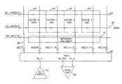
- FIG. 3is a simplified schematic block diagram of a sensing scheme, for matching a reference path to an array path associated with a sense amplifier, in accordance with an embodiment of the present invention.
- FIG. 4is a simplified schematic illustration of the array in accordance with an embodiment of the present invention, showing a detailed connection of an odd sector, its global bit lines and two neighboring global bit lines (from even sectors) to the YMUX.
- FIG. 5is a simplified schematic illustration of the reference mini-array in accordance with an embodiment of the present invention, showing a detailed connection of the reference mini-array to the global bit lines.
- FIGS. 3 , 4 and 5illustrate a sensing scheme for matching a reference path to an array path associated with a sense amplifier, in accordance with an embodiment of the present invention.
- a non-volatile memory cell array 50is shown, which may include a plurality of memory cells 52 connected to word lines 54 and local bit lines 56 ( FIG. 4 ).
- the local bit lines 56are designated by the nomenclature DBL in the drawings.
- the word lines 54are designated by the nomenclature WL in the drawings.
- the local bit lines 56may be connected to GBLs 58 via select transistors 60 (sel_top and sel_bot in FIG. 4 ).
- the array 50may be divided into sectors or slices (discussed further hereinbelow), such as by means of isolation zones.
- a BL driver 64may drive the drain side of the sensed memory cell 52 .
- the BL driver 64may be connected to the sensed cell 52 via a YMUX 66 , via a driving path that includes one of the GBLs 58 , one of the select transistors 60 and one of the local bit lines 56 .
- the connecting line to which the sensed cell 52 is connectedis referred to as the select (SEL) line 65
- the connecting line in the YMUX 66is referred to as BS line 67 ( FIG. 4 ) to which are connected YMUX transistors 69 (designated as bs 0 , bs 1 , etc. in FIG. 4 ).
- a sense amplifier 68may sense the source side of the sensed cell 52 .
- the path from the source of the sensed cell 52 to the sense amplifier 68may be through one of the local bit lines 56 , one of the select transistors 60 , one of the GBLs 58 and the YMUX 66 .
- a reference cell 70may be used for the sense amplifier 68 .
- the reference cell 70may be located in a reference mini-array 72 , which may include word lines 71 and bit lines 73 .
- the present inventionobviates the need for a separate reference bit line driver and a separate reference YMUX.
- the reference mini-array 72may be connected to the same YMUX 66 via a connecting line 74 , referred to as sel_ref_bot, and reference select transistors 76 (ref_bot)
- the reference mini-array 72may be connected to the global bit lines of the array 50 via reference select transistors 76 and 78 , which are selected respectively by reference select lines 74 and 77 .
- Reference select line 74is also referred to as sel_ref_bot
- reference select line 77is also referred to as sel_ref_top.
- the same bit line driver 64may be used to drive the bit lines for both the array cells 52 and the reference cells 70 .
- the array sectorsmay be divided into first and second sectors, referred to as even and odd sectors 62 and 63 , respectively.
- the even and odd sectors 62 and 63have separate even and odd select lines 65 .
- the number of select lines 65is doubled, providing separate access to the even and odd sectors 62 and 63 .
- each of the global bit lines 58can be selected as a drain or source side for the array cell 52 by the YMUX 66 .
- each of the global bit lines 58 of the sense amplifier 68may also be connected to the reference mini-array 72 through the reference select transistors 76 and 78 .
- the YMUX 66may connect the array cells 52 and the reference cell 70 to the sense amplifier 68 using nodes BL_S and BL_REF, respectively.
- the YMUX 66may connect the bit line driver 64 for both the array cells 52 and the reference cell 70 through node BL_D.
- FIG. 4shows one of the odd sectors 63 .
- the explanationfollows for an exemplary array cell 80 , marked by a circle in FIG. 4 , which is sensed with respect to an exemplary reference cell 82 , marked by a circle in FIG. 5 .
- the array cell 80 and the reference cell 82are both dual bit cells, each having right and left bits.
- Sensing the bit on the right hand sidemeans using the bit line DBL[ 3 ] as the drain bit line, and the bit line DBL[ 4 ] as the source bit line. Accordingly, this involves connecting the bit line DBL[ 3 ] to the BL driver 64 via node BL_D, and connecting the bit line DBL[ 4 ] to the sense amplifier 68 via node BL_S. This is achieved by activating the select transistors 60 , sel_top 1 and sel_bot 2 , using the appropriate sel_odd lines 65 .
- the global bit line GBL[ 10 ]is used as the drain GBL, while the global bit line GBL[ 11 ] is used as the source GBL, this being implemented by activating the YMUX transistors bs 4 and bs 8 , which respectively connect global bit line GBL[ 10 ] to node BL_D and global bit line GBL[ 11 ] to node BL_S.
- the global bit line GBL[ 10 ]drives the drain side of both the array cell 80 and the reference cell 82 .
- global bit line GBL[ 10 ]is connected to the drain bit line 73 designated Drain REF_DBL, implemented by activating the ref_top 3 select transistor 78 .
- the global bit line GBL[ 9 ]is selected to be the global bit line that loads the source side of the reference cell 82 (i.e. connecting to the source bit line 73 designated source REF-DBL).
- the global bit line GBL[ 9 ]is selected because both global bit lines GBL[ 9 ] and GBL[ 11 ] are neighbors of the global bit line GBL[ 10 ]. This not only provides matching of the capacitance to ground, but also provides a full match of the coupling between drain and source of the array cell 80 and the reference cell 82 .
- the global bit line GBL[ 9 ]may be selected and connected to the Ref-Source DBL by activating ref-select transistor 76 ref_bot 2 .
- the connection of GBL[ 9 ] to the array 50must be blocked and this may be achieved simply by the aforementioned partition of even and odd sectors. Thus, the connection of GBL[ 9 ] to the array 50 may be blocked by de-activating the sel_even lines.
- the global bit line GBL[ 9 ]may be connected to the sense amplifier 68 via node BL-REF by activating transistor 69 bs 0 in the YMUX 66 .
- Sensing the left side bit of array cell 80means using the bit line DBL[ 4 ] as the drain bit line, and the bit line DBL[ 3 ] as the source bit line. Accordingly, this involves connecting the bit line DBL[ 3 ] to the sense amplifier 68 via node BL_S, and connecting the bit line DBL[ 4 ] to the BL driver 64 via node BL_D. This is achieved by activating the select transistors 60 , sel_top 1 and sel_bot 2 , using the appropriate sel_odd lines 65 .
- the global bit line GBL[ 10 ]is used as the source GBL, while the global bit line GBL[ 11 ] is used as the drain GBL, this being implemented by activating the YMUX transistors bs 7 and bs 5 , which respectively connect global bit line GBL[ 11 ] to node BL_D and global bit line GBL[ 10 ] to node BL_S.
- the global bit line GBL[ 11 ]drives the drain side of both the array cell 80 and the reference cell 82 .
- the global bit line GBL[ 11 ]is connected to the drain bit line 73 designated Drain REF_DBL, implemented by activating the ref_top 4 select transistor 78 .
- the global bit line GBL[ 12 ]is selected to be the global bit line that loads the source side of the reference cell 82 (i.e. connecting to the source bit line 73 designated source REF-DBL).
- the global bit line GBL[ 12 ]is selected because both global bit lines GBL[ 10 ] and GBL[ 12 ] are neighbors of the global bit line GBL[ 11 ].
- the global bit line GBL[ 12 ]may be selected and connected to the Ref-Source DBL by activating ref-select transistor 76 ref_bot 5 .
- the connection of GBL[ 12 ] to the array 50may be blocked by de-activating the sel_even lines.
- the global bit line GBL[ 12 ]may be connected to the sense amplifier 68 via node BL-REF by activating transistor 69 bs 9 in the YMUX 66 .
- the resulting signals generated at the sense amplifier inputswould be the same as the ones shown for the prior art in FIG. 2 . No timing penalty or difference is expected.
- the matchingmay be achieved by using a common drain drive for the array cell and the reference cell, matching the capacitance to ground by using a non-accessed global bit line as a load to the source side of the reference cell, and/or matching the coupling signal between the drain and source by using the neighboring, non-accessed global bit line as the reference global bit line.
- Using a non-accessed global bit line from the array as the reference global bit linemay reduce “real estate” in the chip by eliminating the need for additional reference global bit lines.
- the power consumptionmay be reduced by driving only one drain global bit line for both the array cell and the reference cell as opposed to the prior art which drives two separate global bit lines, one for the array cell and another for the reference cell.
- the present inventionmay require additional select transistors for the reference mini-array 72 , as well as additional decoding for the separate even and odd select lines 65 , which is a small penalty compared to the total outcome.
Landscapes
- Read Only Memory (AREA)
Abstract
Description
Claims (12)
Priority Applications (1)
| Application Number | Priority Date | Filing Date | Title |
|---|---|---|---|
| US11/490,539US7466594B2 (en) | 2004-08-12 | 2006-07-19 | Dynamic matching of signal path and reference path for sensing |
Applications Claiming Priority (2)
| Application Number | Priority Date | Filing Date | Title |
|---|---|---|---|
| US10/916,413US7095655B2 (en) | 2004-08-12 | 2004-08-12 | Dynamic matching of signal path and reference path for sensing |
| US11/490,539US7466594B2 (en) | 2004-08-12 | 2006-07-19 | Dynamic matching of signal path and reference path for sensing |
Related Parent Applications (1)
| Application Number | Title | Priority Date | Filing Date |
|---|---|---|---|
| US10/916,413ContinuationUS7095655B2 (en) | 2004-08-12 | 2004-08-12 | Dynamic matching of signal path and reference path for sensing |
Publications (2)
| Publication Number | Publication Date |
|---|---|
| US20070171717A1 US20070171717A1 (en) | 2007-07-26 |
| US7466594B2true US7466594B2 (en) | 2008-12-16 |
Family
ID=35745840
Family Applications (2)
| Application Number | Title | Priority Date | Filing Date |
|---|---|---|---|
| US10/916,413Expired - Fee RelatedUS7095655B2 (en) | 2004-08-12 | 2004-08-12 | Dynamic matching of signal path and reference path for sensing |
| US11/490,539Expired - LifetimeUS7466594B2 (en) | 2004-08-12 | 2006-07-19 | Dynamic matching of signal path and reference path for sensing |
Family Applications Before (1)
| Application Number | Title | Priority Date | Filing Date |
|---|---|---|---|
| US10/916,413Expired - Fee RelatedUS7095655B2 (en) | 2004-08-12 | 2004-08-12 | Dynamic matching of signal path and reference path for sensing |
Country Status (2)
| Country | Link |
|---|---|
| US (2) | US7095655B2 (en) |
| DE (1) | DE102005037072A1 (en) |
Cited By (2)
| Publication number | Priority date | Publication date | Assignee | Title |
|---|---|---|---|---|
| US20080037336A1 (en)* | 2006-08-11 | 2008-02-14 | Kazuyuki Kouno | Semiconductor memory device |
| US20090290430A1 (en)* | 2008-05-23 | 2009-11-26 | Jack Frayer | Method And Apparatus For Reading And Programming A Non-Volatile Memory Cell In A Virtual Ground Array |
Families Citing this family (18)
| Publication number | Priority date | Publication date | Assignee | Title |
|---|---|---|---|---|
| US6982892B2 (en)* | 2003-05-08 | 2006-01-03 | Micron Technology, Inc. | Apparatus and methods for a physical layout of simultaneously sub-accessible memory modules |
| US20090129166A1 (en)* | 2007-11-15 | 2009-05-21 | Eduardo Maayan | Method, circuit and system for sensing a cell in a non-volatile memory array |
| US7522453B1 (en)* | 2007-12-20 | 2009-04-21 | Actel Corporation | Non-volatile memory with source-side column select |
| US7593265B2 (en) | 2007-12-28 | 2009-09-22 | Sandisk Corporation | Low noise sense amplifier array and method for nonvolatile memory |
| US7957197B2 (en)* | 2008-05-28 | 2011-06-07 | Sandisk Corporation | Nonvolatile memory with a current sense amplifier having a precharge circuit and a transfer gate coupled to a sense node |
| US7830716B2 (en)* | 2008-06-06 | 2010-11-09 | Spansion Llc | Non-volatile memory string module with buffer and method |
| US7838342B2 (en)* | 2008-06-06 | 2010-11-23 | Spansion Llc | Memory device and method |
| US7983089B2 (en)* | 2008-06-06 | 2011-07-19 | Spansion Llc | Sense amplifier with capacitance-coupled differential sense amplifier |
| US8705293B2 (en) | 2011-10-20 | 2014-04-22 | Sandisk Technologies Inc. | Compact sense amplifier for non-volatile memory suitable for quick pass write |
| US8630120B2 (en) | 2011-10-20 | 2014-01-14 | Sandisk Technologies Inc. | Compact sense amplifier for non-volatile memory |
| US8971141B2 (en) | 2012-06-28 | 2015-03-03 | Sandisk Technologies Inc. | Compact high speed sense amplifier for non-volatile memory and hybrid lockout |
| US20140003176A1 (en) | 2012-06-28 | 2014-01-02 | Man Lung Mui | Compact High Speed Sense Amplifier for Non-Volatile Memory with Reduced layout Area and Power Consumption |
| US9293195B2 (en) | 2012-06-28 | 2016-03-22 | Sandisk Technologies Inc. | Compact high speed sense amplifier for non-volatile memory |
| US9741434B2 (en)* | 2013-03-22 | 2017-08-22 | SK Hynix Inc. | Resistance change memory |
| US9208895B1 (en) | 2014-08-14 | 2015-12-08 | Sandisk Technologies Inc. | Cell current control through power supply |
| US9349468B2 (en) | 2014-08-25 | 2016-05-24 | SanDisk Technologies, Inc. | Operational amplifier methods for charging of sense amplifier internal nodes |
| CN114203230B (en) | 2020-09-18 | 2023-09-15 | 长鑫存储技术有限公司 | Column selection signal unit circuit, bit line sensing circuit and memory |
| EP4231301B1 (en) | 2020-09-18 | 2025-07-16 | Changxin Memory Technologies, Inc. | Bit line sense circuit and memory |
Citations (584)
| Publication number | Priority date | Publication date | Assignee | Title |
|---|---|---|---|---|
| GB1297899A (en) | 1970-10-02 | 1972-11-29 | ||
| US3881180A (en) | 1971-11-30 | 1975-04-29 | Texas Instruments Inc | Non-volatile memory cell |
| US3895360A (en) | 1974-01-29 | 1975-07-15 | Westinghouse Electric Corp | Block oriented random access memory |
| US3952325A (en) | 1971-07-28 | 1976-04-20 | U.S. Philips Corporation | Semiconductor memory elements |
| US4016588A (en) | 1974-12-27 | 1977-04-05 | Nippon Electric Company, Ltd. | Non-volatile semiconductor memory device |
| US4017888A (en) | 1975-12-31 | 1977-04-12 | International Business Machines Corporation | Non-volatile metal nitride oxide semiconductor device |
| US4145703A (en) | 1977-04-15 | 1979-03-20 | Supertex, Inc. | High power MOS device and fabrication method therefor |
| JPS5453929U (en) | 1977-09-21 | 1979-04-14 | ||
| US4151021A (en) | 1977-01-26 | 1979-04-24 | Texas Instruments Incorporated | Method of making a high density floating gate electrically programmable ROM |
| US4173791A (en) | 1977-09-16 | 1979-11-06 | Fairchild Camera And Instrument Corporation | Insulated gate field-effect transistor read-only memory array |
| US4173766A (en) | 1977-09-16 | 1979-11-06 | Fairchild Camera And Instrument Corporation | Insulated gate field-effect transistor read-only memory cell |
| US4247861A (en) | 1979-03-09 | 1981-01-27 | Rca Corporation | High performance electrically alterable read-only memory (EAROM) |
| WO1981000790A1 (en) | 1979-09-13 | 1981-03-19 | Ncr Co | Silicon gate non-volatile memory device |
| US4257832A (en) | 1978-07-24 | 1981-03-24 | Siemens Aktiengesellschaft | Process for producing an integrated multi-layer insulator memory cell |
| US4281397A (en) | 1979-10-29 | 1981-07-28 | Texas Instruments Incorporated | Virtual ground MOS EPROM or ROM matrix |
| US4306353A (en) | 1979-06-13 | 1981-12-22 | Siemens Aktiengesellschaft | Process for production of integrated MOS circuits with and without MNOS memory transistors in silicon-gate technology |
| US4342102A (en) | 1980-06-18 | 1982-07-27 | Signetics Corporation | Semiconductor memory array |
| US4342149A (en) | 1979-11-23 | 1982-08-03 | Siemens Aktiengesellschaft | Method of making very short channel length MNOS and MOS devices by double implantation of one conductivity type subsequent to other type implantation |
| US4360900A (en) | 1978-11-27 | 1982-11-23 | Texas Instruments Incorporated | Non-volatile semiconductor memory elements |
| US4373248A (en) | 1978-07-12 | 1983-02-15 | Texas Instruments Incorporated | Method of making high density semiconductor device such as floating gate electrically programmable ROM or the like |
| US4380057A (en) | 1980-10-27 | 1983-04-12 | International Business Machines Corporation | Electrically alterable double dense memory |
| US4388705A (en) | 1981-10-01 | 1983-06-14 | Mostek Corporation | Semiconductor memory circuit |
| US4389705A (en) | 1981-08-21 | 1983-06-21 | Mostek Corporation | Semiconductor memory circuit with depletion data transfer transistor |
| US4404747A (en) | 1981-07-29 | 1983-09-20 | Schur, Inc. | Knife and sheath assembly |
| US4435786A (en) | 1981-11-23 | 1984-03-06 | Fairchild Camera And Instrument Corporation | Self-refreshing memory cell |
| US4448400A (en) | 1981-07-13 | 1984-05-15 | Eliyahou Harari | Highly scalable dynamic RAM cell with self-signal amplification |
| US4471373A (en) | 1980-02-27 | 1984-09-11 | Hitachi, Ltd. | Semiconductor integrated circuit device with memory MISFETS and thin and thick gate insulator MISFETS |
| US4494016A (en) | 1982-07-26 | 1985-01-15 | Sperry Corporation | High performance MESFET transistor for VLSI implementation |
| US4507673A (en) | 1979-10-13 | 1985-03-26 | Tokyo Shibaura Denki Kabushiki Kaisha | Semiconductor memory device |
| US4521796A (en) | 1980-12-11 | 1985-06-04 | General Instrument Corporation | Memory implant profile for improved channel shielding in electrically alterable read only memory semiconductor device |
| US4527257A (en) | 1982-08-25 | 1985-07-02 | Westinghouse Electric Corp. | Common memory gate non-volatile transistor memory |
| JPS60200566A (en) | 1984-03-26 | 1985-10-11 | Hitachi Ltd | Semiconductor integrated circuit device |
| JPS60201594A (en) | 1984-03-23 | 1985-10-12 | Hitachi Micro Comput Eng Ltd | semiconductor storage device |
| GB2157489A (en) | 1984-03-23 | 1985-10-23 | Hitachi Ltd | A semiconductor integrated circuit memory device |
| US4586163A (en) | 1982-09-13 | 1986-04-29 | Toshiba Shibaura Denki Kabushiki Kaisha | Multi-bit-per-cell read only memory circuit |
| US4613956A (en) | 1983-02-23 | 1986-09-23 | Texas Instruments Incorporated | Floating gate memory with improved dielectric |
| US4630085A (en) | 1984-02-28 | 1986-12-16 | Nec Corporation | Erasable, programmable read-only memory device |
| US4663645A (en) | 1984-05-23 | 1987-05-05 | Hitachi, Ltd. | Semiconductor device of an LDD structure having a floating gate |
| US4665426A (en) | 1985-02-01 | 1987-05-12 | Advanced Micro Devices, Inc. | EPROM with ultraviolet radiation transparent silicon nitride passivation layer |
| US4667217A (en) | 1985-04-19 | 1987-05-19 | Ncr Corporation | Two bit vertically/horizontally integrated memory cell |
| US4672409A (en) | 1980-12-25 | 1987-06-09 | Fujitsu Limited | Nonvolatile semiconductor memory device |
| US4725984A (en) | 1984-02-21 | 1988-02-16 | Seeq Technology, Inc. | CMOS eprom sense amplifier |
| US4733105A (en) | 1985-09-04 | 1988-03-22 | Oki Electric Industry Co., Ltd. | CMOS output circuit |
| US4742491A (en) | 1985-09-26 | 1988-05-03 | Advanced Micro Devices, Inc. | Memory cell having hot-hole injection erase mode |
| US4758869A (en) | 1986-08-29 | 1988-07-19 | Waferscale Integration, Inc. | Nonvolatile floating gate transistor structure |
| US4760555A (en) | 1986-04-21 | 1988-07-26 | Texas Instruments Incorporated | Memory array with an array reorganizer |
| US4761764A (en) | 1985-04-18 | 1988-08-02 | Nec Corporation | Programmable read only memory operable with reduced programming power consumption |
| US4769340A (en) | 1983-11-28 | 1988-09-06 | Exel Microelectronics, Inc. | Method for making electrically programmable memory device by doping the floating gate by implant |
| JPS63249375A (en) | 1987-04-06 | 1988-10-17 | Oki Electric Ind Co Ltd | Data erasing method for semiconductor memory device |
| US4780424A (en) | 1987-09-28 | 1988-10-25 | Intel Corporation | Process for fabricating electrically alterable floating gate memory devices |
| US4839705A (en) | 1987-12-16 | 1989-06-13 | Texas Instruments Incorporated | X-cell EEPROM array |
| US4847808A (en) | 1986-04-22 | 1989-07-11 | Nec Corporation | Read only semiconductor memory having multiple bit cells |
| US4857770A (en) | 1988-02-29 | 1989-08-15 | Advanced Micro Devices, Inc. | Output buffer arrangement for reducing chip noise without speed penalty |
| US4870470A (en) | 1987-10-16 | 1989-09-26 | International Business Machines Corporation | Non-volatile memory cell having Si rich silicon nitride charge trapping layer |
| US4888735A (en) | 1987-12-30 | 1989-12-19 | Elite Semiconductor & Systems Int'l., Inc. | ROM cell and array configuration |
| US4916671A (en) | 1988-09-06 | 1990-04-10 | Mitsubishi Denki Kabushiki Kaisha | Semiconductor memory device having sense amplifier having improved activation timing thereof and operating method thereof |
| US4941028A (en) | 1988-08-10 | 1990-07-10 | Actel Corporation | Structure for protecting thin dielectrics during processing |
| US4961010A (en) | 1989-05-19 | 1990-10-02 | National Semiconductor Corporation | Output buffer for reducing switching induced noise |
| US4992391A (en) | 1989-11-29 | 1991-02-12 | Advanced Micro Devices, Inc. | Process for fabricating a control gate for a floating gate FET |
| US5021999A (en) | 1987-12-17 | 1991-06-04 | Mitsubishi Denki Kabushiki Kaisha | Non-volatile semiconductor memory device with facility of storing tri-level data |
| US5027321A (en) | 1989-11-21 | 1991-06-25 | Intel Corporation | Apparatus and method for improved reading/programming of virtual ground EPROM arrays |
| US5029063A (en) | 1989-03-25 | 1991-07-02 | Eurosil Electronic Gmbh | MOSFET multiplying circuit |
| US5042009A (en) | 1988-12-09 | 1991-08-20 | Waferscale Integration, Inc. | Method for programming a floating gate memory device |
| JPH03285358A (en) | 1990-04-02 | 1991-12-16 | Matsushita Electron Corp | Driving method for nonvolatile semiconductor storage device |
| US5075245A (en) | 1990-08-03 | 1991-12-24 | Intel Corporation | Method for improving erase characteristics of buried bit line flash EPROM devices without using sacrificial oxide growth and removal steps |
| US5081371A (en) | 1990-11-07 | 1992-01-14 | U.S. Philips Corp. | Integrated charge pump circuit with back bias voltage reduction |
| US5086325A (en) | 1990-11-21 | 1992-02-04 | Atmel Corporation | Narrow width EEPROM with single diffusion electrode formation |
| US5094968A (en) | 1990-11-21 | 1992-03-10 | Atmel Corporation | Fabricating a narrow width EEPROM with single diffusion electrode formation |
| US5104819A (en) | 1989-08-07 | 1992-04-14 | Intel Corporation | Fabrication of interpoly dielctric for EPROM-related technologies |
| US5117389A (en) | 1990-09-05 | 1992-05-26 | Macronix International Co., Ltd. | Flat-cell read-only-memory integrated circuit |
| US5120672A (en) | 1989-02-22 | 1992-06-09 | Texas Instruments Incorporated | Fabricating a single level merged EEPROM cell having an ONO memory stack substantially spaced from the source region |
| JPH04226071A (en) | 1990-05-16 | 1992-08-14 | Ricoh Co Ltd | Semiconductor memory device |
| US5142496A (en) | 1991-06-03 | 1992-08-25 | Advanced Micro Devices, Inc. | Method for measuring VT 's less than zero without applying negative voltages |
| US5142495A (en) | 1989-03-10 | 1992-08-25 | Intel Corporation | Variable load for margin mode |
| JPH04291982A (en) | 1991-03-20 | 1992-10-16 | Fujitsu Ltd | Light modulator |
| US5159570A (en) | 1987-12-22 | 1992-10-27 | Texas Instruments Incorporated | Four memory state EEPROM |
| US5168334A (en) | 1987-07-31 | 1992-12-01 | Texas Instruments, Incorporated | Non-volatile semiconductor memory |
| US5172338A (en) | 1989-04-13 | 1992-12-15 | Sundisk Corporation | Multi-state EEprom read and write circuits and techniques |
| US5175120A (en) | 1991-10-11 | 1992-12-29 | Micron Technology, Inc. | Method of processing a semiconductor wafer to form an array of nonvolatile memory devices employing floating gate transistors and peripheral area having CMOS transistors |
| US5204835A (en) | 1990-06-13 | 1993-04-20 | Waferscale Integration Inc. | Eprom virtual ground array |
| US5214303A (en) | 1991-02-08 | 1993-05-25 | Sharp Kabushiki Kaisha | Semiconductor device ROM having an offset region |
| JPH0521758Y2 (en) | 1986-05-19 | 1993-06-03 | ||
| US5237213A (en) | 1991-04-15 | 1993-08-17 | Oki Electric Industry Co., Ltd. | Semiconductor integrated circuit with low-noise output buffers |
| US5241497A (en) | 1990-06-14 | 1993-08-31 | Creative Integrated Systems, Inc. | VLSI memory with increased memory access speed, increased memory cell density and decreased parasitic capacitance |
| US5260593A (en) | 1991-12-10 | 1993-11-09 | Micron Technology, Inc. | Semiconductor floating gate device having improved channel-floating gate interaction |
| US5268861A (en) | 1991-04-10 | 1993-12-07 | Sharp Kabushiki Kaisha | Semiconductor read only memory |
| JPH05326893A (en) | 1992-05-25 | 1993-12-10 | Rohm Co Ltd | Non-volatile storage device |
| US5276646A (en) | 1990-09-25 | 1994-01-04 | Samsung Electronics Co., Ltd. | High voltage generating circuit for a semiconductor memory circuit |
| US5280420A (en) | 1992-10-02 | 1994-01-18 | National Semiconductor Corporation | Charge pump which operates on a low voltage power supply |
| US5289412A (en) | 1992-06-19 | 1994-02-22 | Intel Corporation | High-speed bias-stabilized current-mirror referencing circuit for non-volatile memories |
| US5293563A (en) | 1988-12-29 | 1994-03-08 | Sharp Kabushiki Kaisha | Multi-level memory cell with increased read-out margin |
| US5295108A (en) | 1992-04-08 | 1994-03-15 | Nec Corporation | Electrically erasable and programmable read only memory device with simple controller for selecting operational sequences after confirmation |
| US5295092A (en) | 1992-01-21 | 1994-03-15 | Sharp Kabushiki Kaisha | Semiconductor read only memory |
| US5305262A (en) | 1991-09-11 | 1994-04-19 | Kawasaki Steel Corporation | Semiconductor integrated circuit |
| US5311049A (en) | 1991-10-17 | 1994-05-10 | Rohm Co., Ltd. | Non-volatile semiconductor memory with outer drain diffusion layer |
| US5315541A (en) | 1992-07-24 | 1994-05-24 | Sundisk Corporation | Segmented column memory array |
| JPH06151833A (en) | 1992-11-16 | 1994-05-31 | Mitsubishi Electric Corp | Semiconductor device and manufacturing method thereof |
| US5324675A (en) | 1992-03-31 | 1994-06-28 | Kawasaki Steel Corporation | Method of producing semiconductor devices of a MONOS type |
| US5335198A (en) | 1993-05-06 | 1994-08-02 | Advanced Micro Devices, Inc. | Flash EEPROM array with high endurance |
| US5334555A (en) | 1991-11-06 | 1994-08-02 | Sony Corporation | Method of determining conditions for plasma silicon nitride film growth and method of manufacturing semiconductor device |
| US5338954A (en) | 1991-10-31 | 1994-08-16 | Rohm Co., Ltd. | Semiconductor memory device having an insulating film and a trap film joined in a channel region |
| JPH06232416A (en) | 1993-02-03 | 1994-08-19 | Rohm Co Ltd | Semiconductor storage device and manufacture thereof |
| US5345425A (en) | 1990-11-20 | 1994-09-06 | Fujitsu Limited | Semiconductor memory device |
| US5349221A (en) | 1991-10-25 | 1994-09-20 | Rohm Co., Ltd. | Semiconductor memory device and method of reading out information for the same |
| US5350710A (en) | 1993-06-24 | 1994-09-27 | United Microelectronics Corporation | Device for preventing antenna effect on circuit |
| US5352620A (en) | 1984-05-23 | 1994-10-04 | Hitachi, Ltd. | Method of making semiconductor device with memory cells and peripheral transistors |
| US5357134A (en) | 1991-10-31 | 1994-10-18 | Rohm Co., Ltd. | Nonvolatile semiconductor device having charge trap film containing silicon crystal grains |
| US5359554A (en) | 1991-08-27 | 1994-10-25 | Matsushita Electric Industrial Co., Ltd. | Semiconductor memory device having an energy gap for high speed operation |
| US5361343A (en) | 1991-07-30 | 1994-11-01 | Intel Corporation | Microprocessor system including first and second nonvolatile memory arrays which may be simultaneously read and reprogrammed |
| US5366915A (en) | 1992-08-28 | 1994-11-22 | Nec Corporation | Process of fabricating floating gate type field effect transistor having drain region gently varied in impurity profile |
| US5375094A (en) | 1992-06-19 | 1994-12-20 | Kabushiki Kaisha Toshiba | Nonvolatile semiconductor memory system with a plurality of erase blocks |
| US5381374A (en) | 1992-01-09 | 1995-01-10 | Kabushiki Kaisha Toshiba | Memory cell data output circuit having improved access time |
| US5394355A (en) | 1990-08-28 | 1995-02-28 | Mitsubishi Denki Kabushiki Kaisha | Read only memory for storing multi-data |
| US5393701A (en) | 1993-04-08 | 1995-02-28 | United Microelectronics Corporation | Layout design to eliminate process antenna effect |
| US5400286A (en) | 1993-08-17 | 1995-03-21 | Catalyst Semiconductor Corp. | Self-recovering erase scheme to enhance flash memory endurance |
| US5399891A (en) | 1992-01-22 | 1995-03-21 | Macronix International Co., Ltd. | Floating gate or flash EPROM transistor array having contactless source and drain diffusions |
| US5402374A (en) | 1993-04-30 | 1995-03-28 | Rohm Co., Ltd. | Non-volatile semiconductor memory device and memory circuit using the same |
| US5412601A (en) | 1992-08-31 | 1995-05-02 | Nippon Steel Corporation | Non-volatile semiconductor memory device capable of storing multi-value data in each memory cell |
| US5414693A (en) | 1991-08-29 | 1995-05-09 | Hyundai Electronics Industries Co., Ltd. | Self-aligned dual-bit split gate (DSG) flash EEPROM cell |
| US5418743A (en) | 1992-12-07 | 1995-05-23 | Nippon Steel Corporation | Method of writing into non-volatile semiconductor memory |
| US5418176A (en) | 1994-02-17 | 1995-05-23 | United Microelectronics Corporation | Process for producing memory devices having narrow buried N+ lines |
| US5422844A (en) | 1992-12-21 | 1995-06-06 | National Semiconductor Corporation | Memory array with field oxide islands eliminated and method |
| US5424567A (en) | 1991-05-15 | 1995-06-13 | North American Philips Corporation | Protected programmable transistor with reduced parasitic capacitances and method of fabrication |
| US5424978A (en) | 1993-03-15 | 1995-06-13 | Nippon Steel Corporation | Non-volatile semiconductor memory cell capable of storing more than two different data and method of using the same |
| US5426605A (en) | 1992-08-19 | 1995-06-20 | U.S. Philips Corporation | Semiconductor memory device |
| US5434825A (en) | 1988-06-08 | 1995-07-18 | Harari; Eliyahou | Flash EEPROM system cell array with more than two storage states per memory cell |
| US5436478A (en) | 1994-03-16 | 1995-07-25 | National Semiconductor Corporation | Fast access AMG EPROM with segment select transistors which have an increased width |
| US5436481A (en) | 1993-01-21 | 1995-07-25 | Nippon Steel Corporation | MOS-type semiconductor device and method of making the same |
| JPH07193151A (en) | 1993-12-27 | 1995-07-28 | Toshiba Corp | Nonvolatile semiconductor memory device and its storage method |
| US5440505A (en) | 1994-01-21 | 1995-08-08 | Intel Corporation | Method and circuitry for storing discrete amounts of charge in a single memory element |
| US5450341A (en) | 1992-08-31 | 1995-09-12 | Nippon Steel Corporation | Non-volatile semiconductor memory device having memory cells, each for at least three different data writable thereinto selectively and a method of using the same |
| US5450354A (en) | 1992-08-31 | 1995-09-12 | Nippon Steel Corporation | Non-volatile semiconductor memory device detachable deterioration of memory cells |
| US5455793A (en) | 1992-01-15 | 1995-10-03 | National Semiconductor Corp. | Electrically reprogrammable EPROM cell with merged transistor and optimum area |
| US5467308A (en) | 1994-04-05 | 1995-11-14 | Motorola Inc. | Cross-point eeprom memory array |
| US5477499A (en) | 1993-10-13 | 1995-12-19 | Advanced Micro Devices, Inc. | Memory architecture for a three volt flash EEPROM |
| US5495440A (en) | 1993-01-19 | 1996-02-27 | Mitsubishi Denki Kabushiki Kaisha | Semiconductor memory device having hierarchical bit line structure |
| US5496753A (en) | 1992-05-29 | 1996-03-05 | Citizen Watch, Co., Ltd. | Method of fabricating a semiconductor nonvolatile storage device |
| US5508968A (en) | 1994-08-12 | 1996-04-16 | International Business Machines Corporation | Dynamic random access memory persistent page implemented as processor register sets |
| JPH08106791A (en) | 1994-10-03 | 1996-04-23 | Matsushita Electric Ind Co Ltd | Driving method for semiconductor memory device |
| US5518942A (en) | 1995-02-22 | 1996-05-21 | Alliance Semiconductor Corporation | Method of making flash EPROM cell having improved erase characteristics by using a tilt angle implant |
| WO1996015553A1 (en) | 1994-11-15 | 1996-05-23 | Advanced Micro Devices, Inc. | Transistor structure with specific gate and pad areas |
| US5521870A (en) | 1993-12-07 | 1996-05-28 | Nec Corporation | Semiconductor memory device having a coincidence detection circuit and its test method |
| US5523972A (en) | 1994-06-02 | 1996-06-04 | Intel Corporation | Method and apparatus for verifying the programming of multi-level flash EEPROM memory |
| US5523251A (en) | 1994-10-05 | 1996-06-04 | United Microelectronics Corp. | Method for fabricating a self aligned mask ROM |
| US5530803A (en) | 1994-04-14 | 1996-06-25 | Advanced Micro Devices, Inc. | Method and apparatus for programming memory devices |
| US5534804A (en) | 1995-02-13 | 1996-07-09 | Advanced Micro Devices, Inc. | CMOS power-on reset circuit using hysteresis |
| US5537358A (en) | 1994-12-06 | 1996-07-16 | National Semiconductor Corporation | Flash memory having adaptive sensing and method |
| US5544116A (en) | 1993-08-31 | 1996-08-06 | Macronix International Co., Ltd. | Erase and program verification circuit for non-volatile memory |
| US5553018A (en) | 1995-06-07 | 1996-09-03 | Advanced Micro Devices, Inc. | Nonvolatile memory cell formed using self aligned source implant |
| US5553030A (en) | 1993-09-10 | 1996-09-03 | Intel Corporation | Method and apparatus for controlling the output voltage provided by a charge pump circuit |
| US5557570A (en) | 1992-05-28 | 1996-09-17 | Kabushiki Kaisha Toshiba | Nonvolatile semiconductor memory device |
| US5557221A (en) | 1992-06-15 | 1996-09-17 | Fujitsu Limited | Semiconductor integrated circuit with input/output interface adapted for small-amplitude operation |
| US5559687A (en) | 1993-06-21 | 1996-09-24 | Sgs-Thomson Microelectronics, S.R.L. | Voltage multiplier for high output current with stabilized output voltage |
| US5563823A (en) | 1993-08-31 | 1996-10-08 | Macronix International Co., Ltd. | Fast FLASH EPROM programming and pre-programming circuit design |
| US5568085A (en) | 1994-05-16 | 1996-10-22 | Waferscale Integration Inc. | Unit for stabilizing voltage on a capacitive node |
| JPH08297988A (en) | 1995-04-27 | 1996-11-12 | Sony Corp | Semiconductor nonvolatile memory |
| US5579199A (en) | 1992-11-26 | 1996-11-26 | Sharp Kabushiki Kaisha | Non-volatile memory device and a method for producing the same |
| US5581252A (en) | 1994-10-13 | 1996-12-03 | Linear Technology Corporation | Analog-to-digital conversion using comparator coupled capacitor digital-to-analog converters |
| US5583808A (en) | 1994-09-16 | 1996-12-10 | National Semiconductor Corporation | EPROM array segmented for high performance and method for controlling same |
| US5590068A (en) | 1993-02-01 | 1996-12-31 | National Semiconductor Corporation | Ultra-high density alternate metal virtual ground ROM |
| US5590074A (en) | 1991-12-27 | 1996-12-31 | Fujitsu Limited | Nonvolatile semiconductor memory |
| US5592417A (en) | 1994-01-31 | 1997-01-07 | Sgs-Thomson Microelectronics S.A. | Non-volatile programmable bistable multivibrator, programmable by the source, for memory redundancy circuit |
| JPH0917981A (en) | 1995-07-03 | 1997-01-17 | Hitachi Ltd | Semiconductor memory device |
| US5599727A (en) | 1994-12-15 | 1997-02-04 | Sharp Kabushiki Kaisha | Method for producing a floating gate memory device including implanting ions through an oxidized portion of the silicon film from which the floating gate is formed |
| US5600586A (en) | 1994-05-26 | 1997-02-04 | Aplus Integrated Circuits, Inc. | Flat-cell ROM and decoder |
| WO1996025741A3 (en) | 1995-02-16 | 1997-02-06 | Siemens Ag | Multi-valued read-only storage location with improved signal-to-noise ratio |
| US5604804A (en) | 1996-04-23 | 1997-02-18 | Micali; Silvio | Method for certifying public keys in a digital signature scheme |
| US5606523A (en) | 1994-01-31 | 1997-02-25 | Sgs-Thomson Microelectronics S.A. | Non-volatile programmable bistable multivibrator in predefined initial state for memory redundancy circuit |
| US5608679A (en) | 1994-06-02 | 1997-03-04 | Intel Corporation | Fast internal reference cell trimming for flash EEPROM memory |
| US5612642A (en) | 1995-04-28 | 1997-03-18 | Altera Corporation | Power-on reset circuit with hysteresis |
| US5617357A (en) | 1995-04-07 | 1997-04-01 | Advanced Micro Devices, Inc. | Flash EEPROM memory with improved discharge speed using substrate bias and method therefor |
| US5623438A (en) | 1992-11-30 | 1997-04-22 | Sgs-Thomson Microelectronics, Inc. | Virtual ground read only memory circuit |
| US5627790A (en) | 1994-03-22 | 1997-05-06 | Sgs-Thomson Microelectronics S.R.L. | Reading circuit for an integrated semiconductor memory device |
| US5633603A (en) | 1995-12-26 | 1997-05-27 | Hyundai Electronics Industries Co., Ltd. | Data output buffer using pass transistors biased with a reference voltage and a precharged data input |
| US5636288A (en) | 1995-02-16 | 1997-06-03 | Paradigm Electronics Inc. | Standby power circuit arrangement |
| JPH09162314A (en) | 1995-12-12 | 1997-06-20 | Nec Corp | Nonvolatile semiconductor storage device and storage method |
| US5644531A (en) | 1995-11-01 | 1997-07-01 | Advanced Micro Devices, Inc. | Program algorithm for low voltage single power supply flash memories |
| US5650959A (en) | 1994-10-25 | 1997-07-22 | Nkk Corporation | Memory device having virtual ground line |
| US5654568A (en) | 1992-01-17 | 1997-08-05 | Rohm Co., Ltd. | Semiconductor device including nonvolatile memories |
| US5657332A (en) | 1992-05-20 | 1997-08-12 | Sandisk Corporation | Soft errors handling in EEPROM devices |
| US5661060A (en) | 1994-12-28 | 1997-08-26 | National Semiconductor Corporation | Method for forming field oxide regions |
| US5663907A (en) | 1996-04-25 | 1997-09-02 | Bright Microelectronics, Inc. | Switch driver circuit for providing small sector sizes for negative gate erase flash EEPROMS using a standard twin-well CMOS process |
| US5666365A (en) | 1995-03-16 | 1997-09-09 | Bell Atlantic Network Services, Inc. | Simulcast transmission of digital programs to shared antenna receiving systems |
| US5672959A (en) | 1996-04-12 | 1997-09-30 | Micro Linear Corporation | Low drop-out voltage regulator having high ripple rejection and low power consumption |
| US5675280A (en) | 1993-06-17 | 1997-10-07 | Fujitsu Limited | Semiconductor integrated circuit device having built-in step-down circuit for stepping down external power supply voltage |
| US5677869A (en) | 1995-12-14 | 1997-10-14 | Intel Corporation | Programming flash memory using strict ordering of states |
| US5677867A (en) | 1991-06-12 | 1997-10-14 | Hazani; Emanuel | Memory with isolatable expandable bit lines |
| US5683925A (en) | 1996-06-13 | 1997-11-04 | Waferscale Integration Inc. | Manufacturing method for ROM array with minimal band-to-band tunneling |
| US5689459A (en) | 1994-03-03 | 1997-11-18 | Rohm Corporation | Low voltage one transistor flash EEPROM cell using Fowler-Nordheim programming and erase |
| US5694356A (en) | 1994-11-02 | 1997-12-02 | Invoice Technology, Inc. | High resolution analog storage EPROM and flash EPROM |
| US5696929A (en) | 1995-10-03 | 1997-12-09 | Intel Corporation | Flash EEPROM main memory in a computer system |
| US5708608A (en) | 1995-12-28 | 1998-01-13 | Hyundai Electronics Industries Cp., Ltd. | High-speed and low-noise output buffer |
| US5712814A (en) | 1994-07-18 | 1998-01-27 | Sgs-Thomson Microelectronics S.R.L. | Nonvolatile memory cell and a method for forming the same |
| US5712815A (en) | 1996-04-22 | 1998-01-27 | Advanced Micro Devices, Inc. | Multiple bits per-cell flash EEPROM capable of concurrently programming and verifying memory cells and reference cells |
| WO1998003977A1 (en) | 1996-07-23 | 1998-01-29 | Saifun Semiconductors Ltd. | Non-volatile semiconductor memory cell utilizing asymmetrical charge trapping |
| US5715193A (en) | 1996-05-23 | 1998-02-03 | Micron Quantum Devices, Inc. | Flash memory system and method for monitoring the disturb effect on memory cell blocks due to high voltage conditions of other memory cell blocks |
| US5717635A (en) | 1996-08-27 | 1998-02-10 | International Business Machines Corporation | High density EEPROM for solid state file |
| US5717632A (en) | 1996-11-27 | 1998-02-10 | Advanced Micro Devices, Inc. | Apparatus and method for multiple-level storage in non-volatile memories |
| US5717581A (en) | 1994-06-30 | 1998-02-10 | Sgs-Thomson Microelectronics, Inc. | Charge pump circuit with feedback control |
| US5721781A (en) | 1995-09-13 | 1998-02-24 | Microsoft Corporation | Authentication system and method for smart card transactions |
| US5726946A (en) | 1994-06-02 | 1998-03-10 | Mitsubishi Denki Kabushiki Kaisha | Semiconductor integrated circuit device having hierarchical power source arrangement |
| JPH10106276A (en) | 1996-09-30 | 1998-04-24 | Hitachi Ltd | Semiconductor integrated circuit and data processing system |
| US5748534A (en) | 1996-03-26 | 1998-05-05 | Invox Technology | Feedback loop for reading threshold voltage |
| US5751037A (en) | 1995-07-27 | 1998-05-12 | Sony Corporation | Non-volatile memory cell having dual gate electrodes |
| US5751637A (en) | 1995-06-07 | 1998-05-12 | Macronix International Co., Ltd. | Automatic programming algorithm for page mode flash memory with variable programming pulse height and pulse width |
| US5754475A (en) | 1996-06-24 | 1998-05-19 | Advanced Micro Devices, Inc. | Bit line discharge method for reading a multiple bits-per-cell flash EEPROM |
| EP0843398A2 (en) | 1996-11-18 | 1998-05-20 | WaferScale Integration Inc. | Backup battery switch |
| US5760634A (en) | 1996-09-12 | 1998-06-02 | United Microelectronics Corporation | High speed, low noise output buffer |
| US5760445A (en) | 1994-09-13 | 1998-06-02 | Hewlett-Packard Company | Device and method of manufacture for protection against plasma charging damage in advanced MOS technologies |
| US5768193A (en) | 1996-06-17 | 1998-06-16 | Aplus Integrated Circuits, Inc. | Bit-refreshable method and circuit for refreshing a nonvolatile flash memory |
| US5771197A (en) | 1996-06-29 | 1998-06-23 | Hyundai Electronics Industries Co., Ltd. | Sense amplifier of semiconductor memory device |
| US5774395A (en) | 1996-11-27 | 1998-06-30 | Advanced Micro Devices, Inc. | Electrically erasable reference cell for accurately determining threshold voltage of a non-volatile memory at a plurality of threshold voltage levels |
| US5777919A (en) | 1996-09-13 | 1998-07-07 | Holtek Microelectronics, Inc. | Select gate enhanced high density read-only-memory device |
| US5781478A (en) | 1995-11-13 | 1998-07-14 | Kabushiki Kaisha Toshiba | Nonvolatile semiconductor memory device |
| US5781476A (en) | 1989-02-06 | 1998-07-14 | Hitachi, Ltd. | Nonvolatile semiconductor memory device |
| US5784314A (en) | 1995-07-14 | 1998-07-21 | Sgs-Thomson Microelectronics S.R.L. | Method for setting the threshold voltage of a reference memory cell |
| US5783934A (en) | 1995-08-01 | 1998-07-21 | Information Storage Devices, Inc. | CMOS voltage regulator with diode-connected transistor divider circuit |
| US5793079A (en) | 1996-07-22 | 1998-08-11 | Catalyst Semiconductor, Inc. | Single transistor non-volatile electrically alterable semiconductor memory device |
| US5801076A (en) | 1995-02-21 | 1998-09-01 | Advanced Micro Devices, Inc. | Method of making non-volatile memory device having a floating gate with enhanced charge retention |
| US5805500A (en) | 1997-06-18 | 1998-09-08 | Sgs-Thomson Microelectronics S.R.L. | Circuit and method for generating a read reference signal for nonvolatile memory cells |
| US5808506A (en) | 1996-10-01 | 1998-09-15 | Information Storage Devices, Inc. | MOS charge pump generation and regulation method and apparatus |
| US5812456A (en) | 1996-10-01 | 1998-09-22 | Microchip Technology Incorporated | Switched ground read for EPROM memory array |
| US5812457A (en) | 1996-09-09 | 1998-09-22 | Sony Corporation | Semiconductor NAND type flash memory with incremental step pulse programming |
| US5812449A (en) | 1995-05-16 | 1998-09-22 | Hyundai Electronics Industries Co., Ltd. | Flash EEPROM cell, method of manufacturing the same, method of programming and method of reading the same |
| US5815435A (en) | 1995-10-10 | 1998-09-29 | Information Storage Devices, Inc. | Storage cell for analog recording and playback |
| US5822256A (en) | 1994-09-06 | 1998-10-13 | Intel Corporation | Method and circuitry for usage of partially functional nonvolatile memory |
| US5825683A (en) | 1997-10-29 | 1998-10-20 | Utron Technology Inc. | Folded read-only memory |
| US5828601A (en) | 1993-12-01 | 1998-10-27 | Advanced Micro Devices, Inc. | Programmed reference |
| US5835935A (en) | 1995-09-13 | 1998-11-10 | Lexar Media, Inc. | Method of and architecture for controlling system data with automatic wear leveling in a semiconductor non-volatile mass storage memory |
| US5834851A (en) | 1990-02-09 | 1998-11-10 | Hitachi, Ltd. | SRAM having load transistor formed above driver transistor |
| US5836772A (en) | 1994-09-29 | 1998-11-17 | Macronix International Co., Ltd. | Interpoly dielectric process |
| US5841700A (en) | 1992-09-08 | 1998-11-24 | National Semiconductor Corporation | Source-coupling, split gate, virtual ground flash EEPROM array |
| US5847441A (en) | 1996-05-10 | 1998-12-08 | Micron Technology, Inc. | Semiconductor junction antifuse circuit |
| JPH10334676A (en) | 1997-03-31 | 1998-12-18 | Sanyo Electric Co Ltd | Non-volatile semiconductor memory device |
| US5861771A (en) | 1996-10-28 | 1999-01-19 | Fujitsu Limited | Regulator circuit and semiconductor integrated circuit device having the same |
| US5862076A (en) | 1990-11-13 | 1999-01-19 | Waferscale Integration, Inc. | Fast EPROM array |
| US5864164A (en) | 1996-12-09 | 1999-01-26 | United Microelectronics Corp. | Multi-stage ROM structure and method for fabricating the same |
| US5867429A (en) | 1997-11-19 | 1999-02-02 | Sandisk Corporation | High density non-volatile flash memory without adverse effects of electric field coupling between adjacent floating gates |
| US5870335A (en) | 1997-03-06 | 1999-02-09 | Agate Semiconductor, Inc. | Precision programming of nonvolatile memory cells |
| US5870334A (en) | 1994-09-17 | 1999-02-09 | Kabushiki Kaisha Toshiba | Nonvolatile semiconductor memory device |
| US5872848A (en) | 1997-02-18 | 1999-02-16 | Arcanvs | Method and apparatus for witnessed authentication of electronic documents |
| US5875128A (en) | 1996-06-28 | 1999-02-23 | Nec Corporation | Semiconductor memory |
| US5877537A (en) | 1995-12-14 | 1999-03-02 | Sharp Kabushiki Kaisha | Semiconductor device having first transistor rows with second transistor rows connected therebetween |
| US5880620A (en) | 1997-04-22 | 1999-03-09 | Xilinx, Inc. | Pass gate circuit with body bias control |
| US5886927A (en) | 1996-06-11 | 1999-03-23 | Nkk Corporation | Nonvolatile memory device with verify function |
| USRE36179E (en) | 1990-02-13 | 1999-04-06 | Seiko Instruments Inc. | Switching circuit for selecting an output signal from plural input signals |
| US5903031A (en) | 1995-07-04 | 1999-05-11 | Matsushita Electric Industrial Co., Ltd. | MIS device, method of manufacturing the same, and method of diagnosing the same |
| US5910924A (en) | 1996-08-27 | 1999-06-08 | Hitachi, Ltd. | Semiconductor integrated circuit including voltage converter effective at low operational voltages |
| JPH11162182A (en) | 1997-11-27 | 1999-06-18 | Sharp Corp | Nonvolatile semiconductor memory device |
| WO1999031670A2 (en) | 1997-12-12 | 1999-06-24 | Saifun Semiconductors Ltd. | A symmetric segmented memory array architecture |
| US5920503A (en) | 1996-03-29 | 1999-07-06 | Aplus Flash Technology, Inc. | Flash memory with novel bitline decoder and sourceline latch |
| US5926409A (en) | 1997-09-05 | 1999-07-20 | Information Storage Devices, Inc. | Method and apparatus for an adaptive ramp amplitude controller in nonvolatile memory application |
| US5930195A (en) | 1997-10-31 | 1999-07-27 | Sharp Kabushiki Kaisha | Semiconductor memory device |
| US5933367A (en) | 1997-03-18 | 1999-08-03 | Nec Corporation | Erasing method in nonvolatile semiconductor memory device |
| US5933366A (en) | 1996-11-29 | 1999-08-03 | Sanyo Electric Co., Ltd. | Multistate memory device with reference bit lines |
| US5936888A (en) | 1997-07-07 | 1999-08-10 | Nec Corporation | Semiconductor non-volatile memory device having floating gate type reference cell short-circuited between control gate electrode and floating gate electrode |
| US5940332A (en) | 1997-11-13 | 1999-08-17 | Stmicroelectronics, Inc. | Programmed memory with improved speed and power consumption |
| US5946258A (en) | 1998-03-16 | 1999-08-31 | Intel Corporation | Pump supply self regulation for flash memory cell pair reference circuit |
| US5946558A (en) | 1997-02-05 | 1999-08-31 | United Microelectronics Corp. | Method of making ROM components |
| US5949728A (en) | 1997-12-12 | 1999-09-07 | Scenix Semiconductor, Inc. | High speed, noise immune, single ended sensing scheme for non-volatile memories |
| US5959311A (en) | 1998-07-08 | 1999-09-28 | United Microelectronics Corp. | Structure of an antenna effect monitor |
| US5963412A (en) | 1997-11-13 | 1999-10-05 | Advanced Micro Devices, Inc. | Process induced charging damage control device |
| US5966603A (en) | 1997-06-11 | 1999-10-12 | Saifun Semiconductors Ltd. | NROM fabrication method with a periphery portion |
| US5969993A (en) | 1997-06-20 | 1999-10-19 | Nec Corporation | Method of restoring data in non-volatile semiconductor memory |
| US5969989A (en) | 1994-02-02 | 1999-10-19 | Kabushiki Kaisha Toshiba | Semiconductor memory device capable of storing plural-bit data in a single memory cell |
| US5973373A (en) | 1994-09-28 | 1999-10-26 | Siemens Aktiengesellschaft | Read-only-memory cell arrangement using vertical MOS transistors and gate dielectrics of different thicknesses and method for its production |
| US5982666A (en) | 1995-04-28 | 1999-11-09 | Stmicroelectronics S.R.L. | Sense amplifier circuit for semiconductor memory devices |
| WO1999057728A1 (en) | 1998-05-05 | 1999-11-11 | Saifun Semiconductors Ltd. | A two bit rom cell and process for producing same |
| US5986940A (en) | 1997-02-27 | 1999-11-16 | Kabushiki Kaisha Toshiba | Semiconductor integrated circuit device with a constant current source |
| US5990526A (en) | 1997-02-20 | 1999-11-23 | Stmicroelectronics S.R.L. | Memory device with a cell array in triple well, and related manufacturing process |
| US5991202A (en) | 1998-09-24 | 1999-11-23 | Advanced Micro Devices, Inc. | Method for reducing program disturb during self-boosting in a NAND flash memory |
| US5999444A (en) | 1997-09-02 | 1999-12-07 | Sony Corporation | Nonvolatile semiconductor memory device and writing and erasing method of the same |
| US6000006A (en) | 1997-08-25 | 1999-12-07 | Bit Microsystems, Inc. | Unified re-map and cache-index table with dual write-counters for wear-leveling of non-volatile flash RAM mass storage |
| US5999494A (en) | 1993-04-14 | 1999-12-07 | Holzrichter; Dieter | Data recorder |
| US6005423A (en) | 1994-02-10 | 1999-12-21 | Xilinx, Inc. | Low current power-on reset circuit |
| JPH11354758A (en) | 1998-06-08 | 1999-12-24 | Hitachi Ltd | Semiconductor storage device |
| US6011725A (en) | 1997-08-01 | 2000-01-04 | Saifun Semiconductors, Ltd. | Two bit non-volatile electrically erasable and programmable semiconductor memory cell utilizing asymmetrical charge trapping |
| US6018186A (en) | 1997-04-15 | 2000-01-25 | United Microelectronics Corp. | Three-dimensional, deep-trench, high-density read-only memory (ROM) and its manufacturing method |
| US6020241A (en) | 1997-12-22 | 2000-02-01 | Taiwan Semiconductor Manufacturing Company | Post metal code engineering for a ROM |
| US6028324A (en) | 1997-03-07 | 2000-02-22 | Taiwan Semiconductor Manufacturing Company | Test structures for monitoring gate oxide defect densities and the plasma antenna effect |
| US6034403A (en) | 1998-06-25 | 2000-03-07 | Acer Semiconductor Manufacturing, Inc. | High density flat cell mask ROM |
| US6034896A (en) | 1995-07-03 | 2000-03-07 | The University Of Toronto, Innovations Foundation | Method of fabricating a fast programmable flash E2 PROM cell |
| US6037627A (en) | 1996-08-02 | 2000-03-14 | Seiko Instruments Inc. | MOS semiconductor device |
| US6040610A (en) | 1997-04-08 | 2000-03-21 | Kabushiki Kaisha Toshiba | Semiconductor device |
| US6044019A (en) | 1998-10-23 | 2000-03-28 | Sandisk Corporation | Non-volatile memory with improved sensing and method therefor |
| US6044022A (en) | 1999-02-26 | 2000-03-28 | Tower Semiconductor Ltd. | Programmable configuration for EEPROMS including 2-bit non-volatile memory cell arrays |
| US6063666A (en) | 1998-06-16 | 2000-05-16 | Advanced Micro Devices, Inc. | RTCVD oxide and N2 O anneal for top oxide of ONO film |
| US6064226A (en) | 1998-03-17 | 2000-05-16 | Vanguard International Semiconductor Corporation | Multiple input/output level interface input receiver |
| US6064251A (en) | 1997-08-27 | 2000-05-16 | Integrated Silicon Solution, Inc. | System and method for a low voltage charge pump with large output voltage range |
| US6064591A (en) | 1996-04-19 | 2000-05-16 | Kabushiki Kaisha Toshiba | Memory system |
| US6075724A (en) | 1999-02-22 | 2000-06-13 | Vantis Corporation | Method for sorting semiconductor devices having a plurality of non-volatile memory cells |
| US6075402A (en) | 1996-10-11 | 2000-06-13 | Sgs-Thomson Microelectronics S.R.L. | Positive charge pump |
| US6074916A (en) | 1996-04-15 | 2000-06-13 | Sgs-Thomson Microelectronics S.R.L. | FLASH-EPROM with embedded EEPROM |
| US6078518A (en) | 1998-02-25 | 2000-06-20 | Micron Technology, Inc. | Apparatus and method for reading state of multistate non-volatile memory cells |
| US6081456A (en) | 1999-02-04 | 2000-06-27 | Tower Semiconductor Ltd. | Bit line control circuit for a memory array using 2-bit non-volatile memory cells |
| US6084794A (en) | 1999-05-28 | 2000-07-04 | Winbond Electronics Corp. | High speed flat-cell mask ROM structure with select lines |
| US6094095A (en) | 1998-06-29 | 2000-07-25 | Cypress Semiconductor Corp. | Efficient pump for generating voltages above and/or below operating voltages |
| US6097639A (en) | 1997-12-31 | 2000-08-01 | Lg Semicon Co., Ltd. | System and method for programming nonvolatile memory |
| WO2000046808A1 (en) | 1999-02-04 | 2000-08-10 | Saifun Semiconductors Ltd. | Method for initiating a retrieval procedure in virtual ground arrays |
| US6108241A (en) | 1999-07-01 | 2000-08-22 | Micron Technology, Inc. | Leakage detection in flash memory cell |
| US6108240A (en) | 1999-02-04 | 2000-08-22 | Tower Semiconductor Ltd. | Implementation of EEPROM using intermediate gate voltage to avoid disturb conditions |
| US6107862A (en) | 1997-02-28 | 2000-08-22 | Seiko Instruments Inc. | Charge pump circuit |
| US6118207A (en) | 1997-11-12 | 2000-09-12 | Deka Products Limited Partnership | Piezo-electric actuator operable in an electrolytic fluid |
| US6118692A (en) | 1991-02-08 | 2000-09-12 | Btg International Inc. | Memory apparatus including programmable non-volatile multi-bit memory cell, and apparatus and method for demarcating memory states of the cell |
| US6117714A (en) | 1997-12-23 | 2000-09-12 | Intel Corporation | Method for protecting a transistor gate from charge damage |
| US6122198A (en) | 1999-08-13 | 2000-09-19 | Advanced Micro Devices, Inc. | Bit by bit APDE verify for flash memory applications |
| US6128227A (en) | 1998-03-28 | 2000-10-03 | Hyundai Electronics Industries Co., Ltd. | Sense amplifier circuit in a flash memory device |
| US6128226A (en) | 1999-02-04 | 2000-10-03 | Saifun Semiconductors Ltd. | Method and apparatus for operating with a close to ground signal |
| US6130574A (en) | 1997-01-24 | 2000-10-10 | Siemens Aktiengesellschaft | Circuit configuration for producing negative voltages, charge pump having at least two circuit configurations and method of operating a charge pump |
| US6130572A (en) | 1997-01-23 | 2000-10-10 | Stmicroelectronics S.R.L. | NMOS negative charge pump |
| US6130452A (en) | 1997-01-15 | 2000-10-10 | Macronix International Co., Ltd. | Virtual ground flash cell with asymmetrically placed source and drain and method of fabrication |
| US6133095A (en) | 1999-02-04 | 2000-10-17 | Saifun Semiconductors Ltd. | Method for creating diffusion areas for sources and drains without an etch step |
| US6137718A (en) | 1996-08-01 | 2000-10-24 | Siemens Aktiengesellschaft | Method for operating a non-volatile memory cell arrangement |
| US6147904A (en) | 1999-02-04 | 2000-11-14 | Tower Semiconductor Ltd. | Redundancy method and structure for 2-bit non-volatile memory cells |
| US6147906A (en) | 1999-10-14 | 2000-11-14 | Advanced Micro Devices, Inc. | Method and system for saving overhead program time in a memory device |
| US6150800A (en) | 1998-09-16 | 2000-11-21 | Matsushita Electric Industrial Co., Ltd. | Power circuit including inrush current limiter, and integrated circuit including the power circuit |
| US6154081A (en) | 1999-06-15 | 2000-11-28 | Delphi Technologies, Inc. | Load circuit having extended reverse voltage protection |
| US6157242A (en) | 1998-03-19 | 2000-12-05 | Sharp Kabushiki Kaisha | Charge pump for operation at a wide range of power supply voltages |
| US6157570A (en) | 1999-02-04 | 2000-12-05 | Tower Semiconductor Ltd. | Program/erase endurance of EEPROM memory cells |
| US6156149A (en) | 1997-05-07 | 2000-12-05 | Applied Materials, Inc. | In situ deposition of a dielectric oxide layer and anti-reflective coating |
| US6163048A (en) | 1995-10-25 | 2000-12-19 | Cypress Semiconductor Corporation | Semiconductor non-volatile memory device having a NAND cell structure |
| US6163484A (en) | 1998-04-27 | 2000-12-19 | Nec Corporation | Non-volatile semiconductor storage device having improved program/erase/over erase verify |
| US6169691B1 (en) | 1998-09-15 | 2001-01-02 | Stmicroelectronics S.R.L. | Method for maintaining the memory content of non-volatile memory cells |
| US6175519B1 (en) | 1999-07-22 | 2001-01-16 | Macronix International Co., Ltd. | Virtual ground EPROM structure |
| US6175523B1 (en) | 1999-10-25 | 2001-01-16 | Advanced Micro Devices, Inc | Precharging mechanism and method for NAND-based flash memory devices |
| US6181597B1 (en) | 1999-02-04 | 2001-01-30 | Tower Semiconductor Ltd. | EEPROM array using 2-bit non-volatile memory cells with serial read operations |
| US6181605B1 (en) | 1999-10-06 | 2001-01-30 | Advanced Micro Devices, Inc. | Global erase/program verification apparatus and method |
| US6185143B1 (en) | 2000-02-04 | 2001-02-06 | Hewlett-Packard Company | Magnetic random access memory (MRAM) device including differential sense amplifiers |
| US6188211B1 (en) | 1998-05-13 | 2001-02-13 | Texas Instruments Incorporated | Current-efficient low-drop-out voltage regulator with improved load regulation and frequency response |
| US6192445B1 (en) | 1996-09-24 | 2001-02-20 | Altera Corporation | System and method for programming EPROM cells using shorter duration pulse(s) in repeating the programming process of a particular cell |
| US6190966B1 (en) | 1997-03-25 | 2001-02-20 | Vantis Corporation | Process for fabricating semiconductor memory device with high data retention including silicon nitride etch stop layer formed at high temperature with low hydrogen ion concentration |
| US6195196B1 (en) | 1998-03-13 | 2001-02-27 | Fuji Photo Film Co., Ltd. | Array-type exposing device and flat type display incorporating light modulator and driving method thereof |
| US6198342B1 (en) | 1998-12-08 | 2001-03-06 | Sharp Kabushiki Kaisha | Charge pump circuit simple in construction and free from trouble even at low voltage |
| EP1073120A3 (en) | 1999-07-30 | 2001-03-07 | Saifun Semiconductors Ltd | An NROM fabrication method |
| US6201737B1 (en) | 2000-01-28 | 2001-03-13 | Advanced Micro Devices, Inc. | Apparatus and method to characterize the threshold distribution in an NROM virtual ground array |
| US6205055B1 (en) | 2000-02-25 | 2001-03-20 | Advanced Micro Devices, Inc. | Dynamic memory cell programming voltage |
| US6205056B1 (en) | 2000-03-14 | 2001-03-20 | Advanced Micro Devices, Inc. | Automated reference cell trimming verify |
| US6205059B1 (en) | 1998-10-05 | 2001-03-20 | Advanced Micro Devices | Method for erasing flash electrically erasable programmable read-only memory (EEPROM) |
| US6208200B1 (en) | 1997-07-14 | 2001-03-27 | Sony Corporation | Level shift circuit with low voltage operation |
| US6208557B1 (en) | 1999-05-21 | 2001-03-27 | National Semiconductor Corporation | EPROM and flash memory cells with source-side injection and a gate dielectric that traps hot electrons during programming |
| JP2001085646A (en) | 1999-09-10 | 2001-03-30 | Toshiba Corp | Nonvolatile semiconductor memory device |
| US6214666B1 (en) | 1998-12-18 | 2001-04-10 | Vantis Corporation | Method of forming a non-volatile memory device |
| US6215697B1 (en) | 1999-01-14 | 2001-04-10 | Macronix International Co., Ltd. | Multi-level memory cell device and method for self-converged programming |
| US6215702B1 (en) | 2000-02-16 | 2001-04-10 | Advanced Micro Devices, Inc. | Method of maintaining constant erasing speeds for non-volatile memory cells |
| US6215148B1 (en) | 1998-05-20 | 2001-04-10 | Saifun Semiconductors Ltd. | NROM cell with improved programming, erasing and cycling |
| EP1091418A2 (en) | 1999-10-06 | 2001-04-11 | Saifun Semiconductors Ltd | NROM cell with self-aligned programming and erasure areas |
| US6219277B1 (en) | 1998-04-28 | 2001-04-17 | Stmicroelectronics S.A. | Device and method for the reading of EEPROM cells |
| US6219290B1 (en) | 1998-10-14 | 2001-04-17 | Macronix International Co., Ltd. | Memory cell sense amplifier |
| US6218695B1 (en) | 1999-06-28 | 2001-04-17 | Tower Semiconductor Ltd. | Area efficient column select circuitry for 2-bit non-volatile memory cells |
| US6222762B1 (en) | 1992-01-14 | 2001-04-24 | Sandisk Corporation | Multi-state memory |
| US6222768B1 (en) | 2000-01-28 | 2001-04-24 | Advanced Micro Devices, Inc. | Auto adjusting window placement scheme for an NROM virtual ground array |
| JP2001118392A (en) | 1993-08-27 | 2001-04-27 | Toshiba Corp | Nonvolatile semiconductor memory and data programming method thereof |
| US6233180B1 (en) | 1999-02-04 | 2001-05-15 | Saifun Semiconductors Ltd. | Device for determining the validity of word line conditions and for delaying data sensing operation |
| US6240040B1 (en) | 2000-03-15 | 2001-05-29 | Advanced Micro Devices, Inc. | Multiple bank simultaneous operation for a flash memory |
| US6246555B1 (en) | 2000-09-06 | 2001-06-12 | Prominenet Communications Inc. | Transient current and voltage protection of a voltage regulator |
| US6252799B1 (en) | 1997-04-11 | 2001-06-26 | Programmable Silicon Solutions | Device with embedded flash and EEPROM memories |
| US6252442B1 (en) | 1996-09-19 | 2001-06-26 | Sgs-Thomson Microelectronics S.A. | Electronic circuit provided with a neutralization device |
| US6256231B1 (en) | 1999-02-04 | 2001-07-03 | Tower Semiconductor Ltd. | EEPROM array using 2-bit non-volatile memory cells and method of implementing same |
| US20010006477A1 (en) | 1991-02-08 | 2001-07-05 | Banks Gerald J. | Electrically alterable non-volatile memory with n-bits per cell |
| US6261904B1 (en) | 2000-02-10 | 2001-07-17 | Advanced Micro Devices, Inc. | Dual bit isolation scheme for flash devices |
| US6266281B1 (en) | 2000-02-16 | 2001-07-24 | Advanced Micro Devices, Inc. | Method of erasing non-volatile memory cells |
| US6265268B1 (en) | 1999-10-25 | 2001-07-24 | Advanced Micro Devices, Inc. | High temperature oxide deposition process for fabricating an ONO floating-gate electrode in a two bit EEPROM device |
| US6272047B1 (en) | 1999-12-17 | 2001-08-07 | Micron Technology, Inc. | Flash memory cell |
| US6275414B1 (en) | 2000-05-16 | 2001-08-14 | Advanced Micro Devices, Inc. | Uniform bitline strapping of a non-volatile memory cell |
| US6281545B1 (en) | 1997-11-20 | 2001-08-28 | Taiwan Semiconductor Manufacturing Company | Multi-level, split-gate, flash memory cell |
| US6282133B1 (en) | 1999-09-14 | 2001-08-28 | Nec Corporation | Semiconductor memory device having a delay circuit for generating a read timing |
| US6282145B1 (en) | 1999-01-14 | 2001-08-28 | Silicon Storage Technology, Inc. | Array architecture and operating methods for digital multilevel nonvolatile memory integrated circuit system |
| US6285246B1 (en) | 1998-09-15 | 2001-09-04 | California Micro Devices, Inc. | Low drop-out regulator capable of functioning in linear and saturated regions of output driver |
| US6285614B1 (en) | 1997-11-21 | 2001-09-04 | Stmicroelectronics S.R.L. | Voltage regulator for single feed voltage memory circuits, and flash type memory in particular |
| EP0822557B1 (en) | 1996-07-30 | 2001-09-05 | Nec Corporation | Non-volatile semiconductor memory device with variable source voltage |
| US6292394B1 (en) | 2000-06-29 | 2001-09-18 | Saifun Semiconductors Ltd. | Method for programming of a semiconductor memory cell |
| US6297143B1 (en) | 1999-10-25 | 2001-10-02 | Advanced Micro Devices, Inc. | Process for forming a bit-line in a MONOS device |
| US6297974B1 (en) | 1999-09-27 | 2001-10-02 | Intel Corporation | Method and apparatus for reducing stress across capacitors used in integrated circuits |
| US6304485B1 (en) | 1989-04-13 | 2001-10-16 | San Disk Corporation | Flash EEprom system |
| US6307784B1 (en) | 2001-02-28 | 2001-10-23 | Advanced Micro Devices | Negative gate erase |
| US6307807B1 (en) | 1998-09-10 | 2001-10-23 | Kabushiki Kaisha Toshiba | Nonvolatile semiconductor memory |
| US6320786B1 (en) | 2000-12-22 | 2001-11-20 | Macronix International Co., Ltd. | Method of controlling multi-state NROM |
| US6330192B1 (en) | 2000-01-27 | 2001-12-11 | Mitsubishi Denki Kabushiki Kaisha | Nonvolatile semiconductor memory device and method of erasing data of nonvolatile semiconductor memory device |
| US6331950B1 (en) | 1999-10-19 | 2001-12-18 | Fujitsu Limited | Write protect input implementation for a simultaneous operation flash memory device |
| US6335990B1 (en) | 1997-07-03 | 2002-01-01 | Cisco Technology, Inc. | System and method for spatial temporal-filtering for improving compressed digital video |
| US6337502B1 (en) | 1999-06-18 | 2002-01-08 | Saifun Semicinductors Ltd. | Method and circuit for minimizing the charging effect during manufacture of semiconductor devices |
| US20020004921A1 (en) | 2000-07-10 | 2002-01-10 | Hitachi, Ltd. | Method of deciding error rate and semiconductor integrated circuit device |
| US20020004878A1 (en) | 1996-08-08 | 2002-01-10 | Robert Norman | System and method which compares data preread from memory cells to data to be written to the cells |
| US6339556B1 (en) | 1999-11-15 | 2002-01-15 | Nec Corporation | Semiconductor memory device |
| US6343033B1 (en) | 2000-02-25 | 2002-01-29 | Advanced Micro Devices, Inc. | Variable pulse width memory programming |
| US6344959B1 (en) | 1998-05-01 | 2002-02-05 | Unitrode Corporation | Method for sensing the output voltage of a charge pump circuit without applying a load to the output stage |
| US6346442B1 (en) | 1999-02-04 | 2002-02-12 | Tower Semiconductor Ltd. | Methods for fabricating a semiconductor chip having CMOS devices and a fieldless array |
| WO2001065567A3 (en) | 2000-02-29 | 2002-02-14 | Advanced Micro Devices Inc | Selective erasure of a non-volatile memory cell of a flash memory device |
| US6348381B1 (en) | 2001-02-21 | 2002-02-19 | Macronix International Co., Ltd. | Method for forming a nonvolatile memory with optimum bias condition |
| WO2001084552A3 (en) | 2000-05-04 | 2002-02-21 | Saifun Semiconductors Ltd | Programming of nonvolatile memory cells |
| US6351415B1 (en) | 2001-03-28 | 2002-02-26 | Tower Semiconductor Ltd. | Symmetrical non-volatile memory array architecture without neighbor effect |
| US6353554B1 (en) | 1995-02-27 | 2002-03-05 | Btg International Inc. | Memory apparatus including programmable non-volatile multi-bit memory cell, and apparatus and method for demarcating memory states of the cell |
| US6353555B1 (en) | 1999-06-22 | 2002-03-05 | Samsung Electronics Co., Ltd. | Flash memory device capable of minimizing a substrate voltage bouncing and a program method thereof |
| US6353356B1 (en) | 1999-08-30 | 2002-03-05 | Micron Technology, Inc. | High voltage charge pump circuits |
| US6356469B1 (en) | 2000-09-14 | 2002-03-12 | Fairchild Semiconductor Corporation | Low voltage charge pump employing optimized clock amplitudes |
| US6356062B1 (en) | 2000-09-27 | 2002-03-12 | Intel Corporation | Degenerative load temperature correction for charge pumps |
| US6359501B2 (en) | 2000-02-11 | 2002-03-19 | Windbond Eelctronics Corp. | Charge-pumping circuits for a low-supply voltage |
| US6374337B1 (en) | 1998-11-17 | 2002-04-16 | Lexar Media, Inc. | Data pipelining method and apparatus for memory control circuit |
| WO2001065566A3 (en) | 2000-02-29 | 2002-04-18 | Advanced Micro Devices Inc | Selective erasure of a non-volatile memory cell of a flash memory device |
| US6385086B1 (en) | 2000-06-13 | 2002-05-07 | Mitsubishi Denki Kabushiki Kaisha | Nonvolatile semiconductor memory device capable of high speed generation of rewrite voltage |
| WO2002043073A1 (en) | 2000-11-21 | 2002-05-30 | Advanced Micro Devices, Inc. | Method and system for dual bit memory erase verification |
| US20020064911A1 (en) | 1997-07-30 | 2002-05-30 | Boaz Eitan | Non-volatile electrically erasable and programmable semiconductor memory cell utilizing asymmetrical charge trapping |
| US6400607B1 (en) | 1999-10-29 | 2002-06-04 | Stmicroelectronics S.R.L. | Reading circuit for a non-volatile memory |
| US6400209B1 (en) | 1999-08-05 | 2002-06-04 | Fujitsu Limited | Switch circuit with back gate voltage control and series regulator |
| US6407537B2 (en) | 1999-12-21 | 2002-06-18 | Koninklijke Philips Electronics N.V. | Voltage regulator provided with a current limiter |
| US6410388B1 (en) | 2000-02-15 | 2002-06-25 | Advanced Micro Devices, Inc. | Process for optimizing pocket implant profile by RTA implant annealing for a non-volatile semiconductor device |
| US6417081B1 (en) | 2000-05-16 | 2002-07-09 | Advanced Micro Devices, Inc. | Process for reduction of capacitance of a bitline for a non-volatile memory cell |
| US6418506B1 (en) | 1996-12-31 | 2002-07-09 | Intel Corporation | Integrated circuit memory and method for transferring data using a volatile memory to buffer data for a nonvolatile memory array |
| US6426898B1 (en) | 2001-03-05 | 2002-07-30 | Micron Technology, Inc. | Method of reducing trapped holes induced by erase operations in the tunnel oxide of flash memory cells |
| JP2002216488A (en) | 2001-01-18 | 2002-08-02 | Iwate Toshiba Electronics Co Ltd | Semiconductor storage device |
| US6429063B1 (en) | 1999-10-26 | 2002-08-06 | Saifun Semiconductors Ltd. | NROM cell with generally decoupled primary and secondary injection |
| US6433624B1 (en) | 2000-11-30 | 2002-08-13 | Intel Corporation | Threshold voltage generation circuit |
| US6438035B2 (en) | 2000-06-15 | 2002-08-20 | Sharp Kabushiki Kaisha | Nonvolatile semiconductor storage device |
| US6436766B1 (en) | 1999-10-29 | 2002-08-20 | Advanced Micro Devices, Inc. | Process for fabricating high density memory cells using a polysilicon hard mask |
| US6438031B1 (en) | 2000-02-16 | 2002-08-20 | Advanced Micro Devices, Inc. | Method of programming a non-volatile memory cell using a substrate bias |
| US6436768B1 (en) | 2001-06-27 | 2002-08-20 | Advanced Micro Devices, Inc. | Source drain implant during ONO formation for improved isolation of SONOS devices |
| US6440797B1 (en) | 2001-09-28 | 2002-08-27 | Advanced Micro Devices, Inc. | Nitride barrier layer for protection of ONO structure from top oxide loss in a fabrication of SONOS flash memory |
| US6442074B1 (en) | 2001-02-28 | 2002-08-27 | Advanced Micro Devices, Inc. | Tailored erase method using higher program VT and higher negative gate erase |
| US6445030B1 (en) | 2001-01-30 | 2002-09-03 | Advanced Micro Devices, Inc. | Flash memory erase speed by fluorine implant or fluorination |
| US6448750B1 (en) | 2001-04-05 | 2002-09-10 | Saifun Semiconductor Ltd. | Voltage regulator for non-volatile memory with large power supply rejection ration and minimal current drain |
| US6449190B1 (en) | 2001-01-17 | 2002-09-10 | Advanced Micro Devices, Inc. | Adaptive reference cells for a memory device |
| US6449188B1 (en) | 2001-06-19 | 2002-09-10 | Advanced Micro Devices, Inc. | Low column leakage nor flash array-double cell implementation |
| US6452438B1 (en) | 2000-12-28 | 2002-09-17 | Intel Corporation | Triple well no body effect negative charge pump |
| US20020132436A1 (en) | 2001-01-18 | 2002-09-19 | Ron Eliyahu | EEPROM array and method for operation thereof |
| US6456528B1 (en) | 2001-09-17 | 2002-09-24 | Sandisk Corporation | Selective operation of a multi-state non-volatile memory system in a binary mode |
| US6455896B1 (en) | 2001-04-25 | 2002-09-24 | Macronix International Co., Ltd. | Protection circuit for a memory array |
| US6456533B1 (en) | 2001-02-28 | 2002-09-24 | Advanced Micro Devices, Inc. | Higher program VT and faster programming rates based on improved erase methods |
| US6458656B1 (en) | 2000-03-16 | 2002-10-01 | Advanced Micro Devices, Inc. | Process for creating a flash memory cell using a photoresist flow operation |
| US6458677B1 (en) | 1999-10-25 | 2002-10-01 | Advanced Micro Devices, Inc. | Process for fabricating an ONO structure |
| EP0693781B1 (en) | 1994-07-13 | 2002-10-02 | United Microelectronics Corporation | Grounding method for eliminating process antenna effect |
| US20020140109A1 (en) | 1999-12-22 | 2002-10-03 | Ali Keshavarzi | Decoupling capacitors for thin gate oxides |
| US20020145465A1 (en) | 2001-04-05 | 2002-10-10 | Joseph Shor | Efficient charge pump apparatus and method for operating the same |
| US6469935B2 (en) | 1999-08-05 | 2002-10-22 | Halo Lsi Design & Device Technology, Inc. | Array architecture nonvolatile memory and its operation methods |
| US6469929B1 (en) | 2001-08-21 | 2002-10-22 | Tower Semiconductor Ltd. | Structure and method for high speed sensing of memory arrays |
| US6472706B2 (en) | 2000-07-12 | 2002-10-29 | Koninklijke Philips Electronics Nv | Semiconductor device |
| US6477085B1 (en) | 2001-05-09 | 2002-11-05 | Macronix International Co., Ltd. | Method for operating non-volatile memory with symmetrical dual-channels |
| EP0751560B1 (en) | 1995-06-30 | 2002-11-27 | STMicroelectronics S.r.l. | Process for forming an integrated circuit comprising non-volatile memory cells and side transistors of at least two different types, and corresponding IC |
| US6490204B2 (en) | 2000-05-04 | 2002-12-03 | Saifun Semiconductors Ltd. | Programming and erasing methods for a reference cell of an NROM array |
| US6496414B2 (en) | 2001-04-20 | 2002-12-17 | Fujitsu Limited | Nonvolatile semiconductor memory |
| US20020191465A1 (en) | 2001-04-25 | 2002-12-19 | Eduardo Maayan | Method for operation of an EEPROM array, including refresh thereof |
| US20020199065A1 (en) | 2001-06-20 | 2002-12-26 | Sreenivas Subramoney | Method for using cache prefetch feature to improve garbage collection algorithm |
| US20030001213A1 (en) | 2001-06-29 | 2003-01-02 | Chinatech Corporation | High density read only memory and fabrication method thereof |
| US6504756B2 (en) | 1998-04-08 | 2003-01-07 | Micron Technology, Inc. | Dual floating gate programmable read only memory cell structure and method for its fabrication and operation |
| US6510082B1 (en) | 2001-10-23 | 2003-01-21 | Advanced Micro Devices, Inc. | Drain side sensing scheme for virtual ground flash EPROM array with adjacent bit charge and hold |
| US6512701B1 (en) | 2001-06-21 | 2003-01-28 | Advanced Micro Devices, Inc. | Erase method for dual bit virtual ground flash |
| US20030021155A1 (en) | 2001-04-09 | 2003-01-30 | Yachareni Santosh K. | Soft program and soft program verify of the core cells in flash memory array |
| US6519182B1 (en) | 2000-07-10 | 2003-02-11 | Advanced Micro Devices, Inc. | Using hot carrier injection to control over-programming in a non-volatile memory cell having an oxide-nitride-oxide (ONO) structure |
| US6522585B2 (en) | 2001-05-25 | 2003-02-18 | Sandisk Corporation | Dual-cell soft programming for virtual-ground memory arrays |
| US6525969B1 (en) | 2001-08-10 | 2003-02-25 | Advanced Micro Devices, Inc. | Decoder apparatus and methods for pre-charging bit lines |
| US6529412B1 (en) | 2002-01-16 | 2003-03-04 | Advanced Micro Devices, Inc. | Source side sensing scheme for virtual ground read of flash eprom array with adjacent bit precharge |
| US6528390B2 (en) | 2001-03-02 | 2003-03-04 | Advanced Micro Devices, Inc. | Process for fabricating a non-volatile memory device |
| US6532173B2 (en) | 2001-07-10 | 2003-03-11 | Fujitsu Limited | Nonvolatile semiconductor memory device with mechanism to prevent leak current |
| US6535020B1 (en) | 2001-12-18 | 2003-03-18 | Sun Microsystems, Inc. | Output buffer with compensated slew rate and delay control |
| US6535434B2 (en) | 2001-04-05 | 2003-03-18 | Saifun Semiconductors Ltd. | Architecture and scheme for a non-strobed read sequence |
| US6538270B1 (en) | 2000-05-16 | 2003-03-25 | Advanced Micro Devices, Inc. | Staggered bitline strapping of a non-volatile memory cell |
| US6537881B1 (en) | 2000-10-16 | 2003-03-25 | Advanced Micro Devices, Inc. | Process for fabricating a non-volatile memory device |
| US6541816B2 (en) | 2000-11-28 | 2003-04-01 | Advanced Micro Devices, Inc. | Planar structure for non-volatile memory devices |
| US20030076710A1 (en) | 2001-10-24 | 2003-04-24 | Yair Sofer | Method for erasing a memory cell |
| US6559500B2 (en) | 2001-03-29 | 2003-05-06 | Fujitsu Limited | Non-volatile semiconductor memory and its driving method |
| US6562683B1 (en) | 2000-08-31 | 2003-05-13 | Advanced Micro Devices, Inc. | Bit-line oxidation by removing ONO oxide prior to bit-line implant |
| US6567312B1 (en) | 2000-05-15 | 2003-05-20 | Fujitsu Limited | Non-volatile semiconductor memory device having a charge storing insulation film and data holding method therefor |
| US6567303B1 (en) | 2001-01-31 | 2003-05-20 | Advanced Micro Devices, Inc. | Charge injection |
| US6566194B1 (en) | 2001-10-01 | 2003-05-20 | Advanced Micro Devices, Inc. | Salicided gate for virtual ground arrays |
| US6570211B1 (en) | 2002-06-26 | 2003-05-27 | Advanced Micro Devices, Inc. | 2Bit/cell architecture for floating gate flash memory product and associated method |
| US6574139B2 (en) | 2001-06-20 | 2003-06-03 | Fujitsu Limited | Method and device for reading dual bit memory cells using multiple reference cells with two side read |
| US6577547B2 (en) | 2001-01-16 | 2003-06-10 | Umc Japan | Semiconductor memory device |
| US6577514B2 (en) | 2001-04-05 | 2003-06-10 | Saifun Semiconductors Ltd. | Charge pump with constant boosted output voltage |
| US6577532B1 (en) | 1996-10-24 | 2003-06-10 | Micron Technology, Inc. | Method for performing analog over-program and under-program detection for a multistate memory cell |
| US6584017B2 (en) | 2001-04-05 | 2003-06-24 | Saifun Semiconductors Ltd. | Method for programming a reference cell |
| US6583479B1 (en) | 2000-10-16 | 2003-06-24 | Advanced Micro Devices, Inc. | Sidewall NROM and method of manufacture thereof for non-volatile memory cells |
| US6583007B1 (en) | 2001-12-20 | 2003-06-24 | Saifun Semiconductors Ltd. | Reducing secondary injection effects |
| US6583005B2 (en) | 2000-08-01 | 2003-06-24 | Fujitsu Limited | Method of manufacturing a semiconductor memory device with a buried bit line |
| US20030117841A1 (en) | 2000-08-03 | 2003-06-26 | Fujitsu Limited | Non-volatile semiconductor storage device and method of reading out data |
| US20030131186A1 (en) | 2001-12-29 | 2003-07-10 | Wolfgang Buhr | Method and arrangement for programming and verifying EEPROM pages and a corresponding computer software product and a corresponding computer-readable storage medium |
| US6593606B1 (en) | 2000-05-16 | 2003-07-15 | Advanced Micro Devices, Inc. | Staggered bitline strapping of a non-volatile memory cell |
| US6594181B1 (en) | 2002-05-10 | 2003-07-15 | Fujitsu Limited | System for reading a double-bit memory cell |
| US20030134476A1 (en) | 2002-01-17 | 2003-07-17 | Yakov Roizin | Oxide-nitride-oxide structure |
| US20030145188A1 (en) | 2002-01-31 | 2003-07-31 | Zeev Cohen | Look ahead methods and apparatus |
| US20030142544A1 (en) | 2002-01-31 | 2003-07-31 | Eduardo Maayan | Mass storage array and methods for operation thereof |
| US20030145176A1 (en) | 2002-01-31 | 2003-07-31 | Ran Dvir | Mass storage device architecture and operation |
| US6608905B1 (en) | 1997-12-19 | 2003-08-19 | Texas Instruments Incorporated | Microphone bias current measurement circuit |
| US6608526B1 (en) | 2002-04-17 | 2003-08-19 | National Semiconductor Corporation | CMOS assisted output stage |
| US20030155659A1 (en) | 2002-02-19 | 2003-08-21 | Vani Verma | Memory module having interconnected and stacked integrated circuits |
| US6614052B1 (en) | 1995-11-07 | 2003-09-02 | Semiconductor Energy Laboratory Co., Ltd. | Semiconductor display devices and applications |
| US6614686B1 (en) | 1999-10-14 | 2003-09-02 | Fujitsu Limited | Nonvolatile memory circuit for recording multiple bit information |
| US6614295B2 (en) | 2000-12-28 | 2003-09-02 | Nec Corporation | Feedback-type amplifier circuit and driver circuit |
| US6617215B1 (en) | 2002-03-27 | 2003-09-09 | Advanced Micro Devices, Inc. | Memory wordline hard mask |
| US6618290B1 (en) | 2000-06-23 | 2003-09-09 | Advanced Micro Devices, Inc. | Method of programming a non-volatile memory cell using a baking process |
| US6617179B1 (en) | 2001-06-05 | 2003-09-09 | Advanced Micro Devices, Inc. | Method and system for qualifying an ONO layer in a semiconductor device |
| US6624672B2 (en) | 2000-12-21 | 2003-09-23 | Stmicroelectronics S.R.L. | Output buffer with constant switching current |
| EP1071096B1 (en) | 1999-07-22 | 2003-09-24 | STMicroelectronics S.r.l. | Read circuit for a nonvolatile memory |
| WO2003079370A1 (en) | 2002-03-13 | 2003-09-25 | Advanced Micro Devices, Inc. | Overerase correction method |
| WO2003079446A1 (en) | 2002-03-14 | 2003-09-25 | Spansion, Llc | Hard mask process for memory device without bitline shorts |
| US6630384B1 (en) | 2001-10-05 | 2003-10-07 | Advanced Micro Devices, Inc. | Method of fabricating double densed core gates in sonos flash memory |
| WO2003083916A1 (en) | 2002-03-27 | 2003-10-09 | Spansion, Llc | Memory wordline hard mask extension |
| US20030190786A1 (en) | 2002-04-08 | 2003-10-09 | Ramsbey Mark T. | Memory manufacturing process with bitline isolation |
| US6633956B1 (en) | 2000-04-14 | 2003-10-14 | Mitsubishi Denki Kabushiki Kaisha | Memory card with task registers storing physical addresses |
| US6633496B2 (en) | 1997-12-12 | 2003-10-14 | Saifun Semiconductors Ltd. | Symmetric architecture for memory cells having widely spread metal bit lines |
| US6633499B1 (en) | 1997-12-12 | 2003-10-14 | Saifun Semiconductors Ltd. | Method for reducing voltage drops in symmetric array architectures |
| WO2003088261A1 (en) | 2002-04-12 | 2003-10-23 | Advance Micro Devices, Int. | System and method for generating a reference voltage based on averaging the voltages of two complementary programmed dual bit reference cells |
| WO2003088258A1 (en) | 2002-04-08 | 2003-10-23 | Advanced Micro Devices, Inc. | Improved erase method for a dual bit memory cell |
| WO2003088260A1 (en) | 2002-04-08 | 2003-10-23 | Advanced Micro Devices, Inc. | Algorithm dynamic reference programming |
| WO2003088259A1 (en) | 2002-04-08 | 2003-10-23 | Advanced Micro Devices, Inc. | Refresh scheme for dynamic page programming |
| US20030197221A1 (en) | 2002-04-17 | 2003-10-23 | Fujitsu Limited | Non-volatile semiconductor memory and method of manufacturing the same |
| US6639271B1 (en) | 2001-12-20 | 2003-10-28 | Advanced Micro Devices, Inc. | Fully isolated dielectric memory cell structure for a dual bit nitride storage device and process for making same |
| US6639837B2 (en) | 2000-12-11 | 2003-10-28 | Kabushiki Kaisha Toshiba | Non-volatile semiconductor memory device |
| US6639849B2 (en) | 2002-02-28 | 2003-10-28 | Fujitsu Limited | Nonvolatile semiconductor memory device programming second dynamic reference cell according to threshold value of first dynamic reference cell |
| US20030202411A1 (en) | 2002-04-29 | 2003-10-30 | Shigekazu Yamada | System for control of pre-charge levels in a memory device |
| US6643170B2 (en) | 2001-10-24 | 2003-11-04 | Macronix International Co., Ltd. | Method for operating a multi-level memory cell |
| US6642148B1 (en) | 2002-04-19 | 2003-11-04 | Advanced Micro Devices, Inc. | RELACS shrink method applied for single print resist mask for LDD or buried bitline implants using chemically amplified DUV type photoresist |
| US6642586B2 (en) | 2001-02-07 | 2003-11-04 | Fujitsu Limited | Semiconductor memory capable of being driven at low voltage and its manufacture method |
| US6643178B2 (en) | 2001-07-31 | 2003-11-04 | Fujitsu Limited | System for source side sensing |
| US6642573B1 (en) | 2002-03-13 | 2003-11-04 | Advanced Micro Devices, Inc. | Use of high-K dielectric material in modified ONO structure for semiconductor devices |
| US6643177B1 (en) | 2003-01-21 | 2003-11-04 | Advanced Micro Devices, Inc. | Method for improving read margin in a flash memory device |
| US20030206435A1 (en) | 2000-12-21 | 2003-11-06 | Fujitsu Limited | Nonvolatile semiconductor storage device and data erasing method |
| US6645801B1 (en) | 2001-10-01 | 2003-11-11 | Advanced Micro Devices, Inc. | Salicided gate for virtual ground arrays |
| US20030209767A1 (en) | 2002-05-10 | 2003-11-13 | Fujitsu Limited | Nonvolatile semiconductor memory device and method for fabricating the same |
| US6650568B2 (en) | 2001-02-26 | 2003-11-18 | Fujitsu Limited | Method of read operation of nonvolatile semiconductor memory and nonvolatile semiconductor memory |
| US20030214844A1 (en) | 2002-05-15 | 2003-11-20 | Fujitsu Limited | Nonvolatile semiconductor memory device of virtual-ground memory array with reliable data reading |
| US6653190B1 (en) | 2001-12-15 | 2003-11-25 | Advanced Micro Devices, Inc. | Flash memory with controlled wordline width |
| US6653191B1 (en) | 2002-05-16 | 2003-11-25 | Advanced Micro Devices, Inc. | Memory manufacturing process using bitline rapid thermal anneal |
| US6654296B2 (en) | 2001-07-23 | 2003-11-25 | Samsung Electronics Co., Ltd. | Devices, circuits and methods for dual voltage generation using single charge pump |
| EP1365452A2 (en) | 2002-05-21 | 2003-11-26 | Fujitsu Limited | Non-volatile semiconductor memory device and method of fabricating thereof |
| US20030218913A1 (en) | 2002-05-24 | 2003-11-27 | Le Binh Quang | Stepped pre-erase voltages for mirrorbit erase |
| US20030222303A1 (en) | 2002-05-31 | 2003-12-04 | Fujitsu Limited | Non-volatile semiconductor memory device and method for fabricating the same |
| WO2003063167A3 (en) | 2002-01-16 | 2003-12-04 | Advanced Micro Devices Inc | System and method for programming ono dual bit memory cells |
| US20030227796A1 (en) | 2002-06-11 | 2003-12-11 | Fujitsu Limited | Nonvolatile semiconductor memory device capable of correcting over-erased memory cells |
| US6665769B2 (en) | 2001-04-05 | 2003-12-16 | Saifun Semiconductors Ltd. | Method and apparatus for dynamically masking an N-bit memory array having individually programmable cells |
| US6670669B1 (en) | 1999-08-10 | 2003-12-30 | Fujitsu Limited | Multiple-bit non-volatile memory utilizing non-conductive charge trapping gate |
| US6670241B1 (en) | 2002-04-22 | 2003-12-30 | Advanced Micro Devices, Inc. | Semiconductor memory with deuterated materials |
| US6674138B1 (en) | 2001-12-31 | 2004-01-06 | Advanced Micro Devices, Inc. | Use of high-k dielectric materials in modified ONO structure for semiconductor devices |
| US6677805B2 (en) | 2001-04-05 | 2004-01-13 | Saifun Semiconductors Ltd. | Charge pump stage with body effect minimization |
| US20040007730A1 (en) | 2002-07-15 | 2004-01-15 | Macronix International Co., Ltd. | Plasma damage protection circuit for a semiconductor device |
| US20040012993A1 (en) | 2002-07-16 | 2004-01-22 | Kazuhiro Kurihara | System for using a dynamic reference in a double-bit cell memory |
| US20040014280A1 (en) | 2002-07-22 | 2004-01-22 | Josef Willer | Non-Volatile memory cell and fabrication method |
| US20040013000A1 (en) | 2002-07-16 | 2004-01-22 | Fujitsu Limited | Nonvolatile semiconductor memory and method of operating the same |
| US6686242B2 (en) | 2001-03-02 | 2004-02-03 | Infineon Technologies Ag | Method for producing metallic bit lines for memory cell arrays, method for producing memory cell arrays and memory cell array |
| US20040027858A1 (en) | 2002-08-12 | 2004-02-12 | Fujitsu Limited | Nonvolatile memory having a trap layer |
| US6693483B2 (en) | 2000-04-11 | 2004-02-17 | Infineon Technologies Ag | Charge pump configuration having closed-loop control |
| US6700818B2 (en) | 2002-01-31 | 2004-03-02 | Saifun Semiconductors Ltd. | Method for operating a memory device |
| WO2003054964A3 (en) | 2001-12-20 | 2004-03-04 | Fasl Llc | Monos device having buried metal silicide bit line |
| US6717207B2 (en) | 2002-01-30 | 2004-04-06 | Renesas Technology Corp. | Non-volatile semiconductor memory device of which bit line withstand voltage can be increased |
| US6723518B2 (en) | 1998-01-20 | 2004-04-20 | Codon Diagnostics, Llc | Detection and treatment of breast disease |
| US6731542B1 (en) | 2002-12-05 | 2004-05-04 | Advanced Micro Devices, Inc. | Circuit for accurate memory read operations |
| US6738289B2 (en) | 2001-02-26 | 2004-05-18 | Sandisk Corporation | Non-volatile memory with improved programming and method therefor |
| US6744692B2 (en) | 2002-02-07 | 2004-06-01 | Renesas Technology Corp. | Memory system's improvement in efficiency of data process between host, buffer memory and nonvolatile memory |
| US6765259B2 (en) | 2002-08-28 | 2004-07-20 | Tower Semiconductor Ltd. | Non-volatile memory transistor array implementing “H” shaped source/drain regions and method for fabricating same |
| US20040153821A1 (en) | 2002-12-04 | 2004-08-05 | Juergen Kuhmann | Error condition handling |
| US20040151034A1 (en) | 2003-01-30 | 2004-08-05 | Shor Joseph S. | Method and circuit for operating a memory cell using a single charge pump |
| US20040157393A1 (en) | 2003-02-10 | 2004-08-12 | Macronix International Co., Ltd. | Method for manufacturing embedded non-volatile memory with two polysilicon layers |
| US6781876B2 (en) | 1997-07-29 | 2004-08-24 | Micron Technology, Inc. | Memory device with gallium nitride or gallium aluminum nitride gate |
| US6788579B2 (en) | 2001-04-10 | 2004-09-07 | Stmicroelectronics S.R.L. | Method for programming nonvolatile memory cells with program and verify algorithm using a staircase voltage with varying step amplitude |
| US6791396B2 (en) | 2001-10-24 | 2004-09-14 | Saifun Semiconductors Ltd. | Stack element circuit |
| US6794249B2 (en) | 2001-06-21 | 2004-09-21 | Infineon Technologies Ag | Method for fabricating a memory cell |
| US6794280B2 (en) | 2003-01-22 | 2004-09-21 | Macronix International Co., Ltd. | Method of fabricating non-volatile memory |
| US20040222437A1 (en) | 2000-12-07 | 2004-11-11 | Dror Avni | Programming and erasing methods for an NROM array |
| US6818956B2 (en) | 2002-03-20 | 2004-11-16 | Macronix International Co., Ltd. | Non-volatile memory device and fabrication method thereof |
| US6831872B2 (en) | 2002-12-04 | 2004-12-14 | Sharp Kabushiki Kaisha | Semiconductor memory device and method for correcting a reference cell |
| US6836431B2 (en) | 2001-06-29 | 2004-12-28 | Hynix Semiconductor Inc | Method of programming/reading multi-level flash memory using sensing circuit |
| US6859028B2 (en) | 2002-11-26 | 2005-02-22 | Sige Semiconductor Inc. | Design-for-test modes for a phase locked loop |
| US6871258B2 (en) | 2001-06-05 | 2005-03-22 | Stmicroelectronics S.R.L. | Method for erasing an electrically erasable nonvolatile memory device, in particular an eeprom-flash memory device, and an electrically erasable nonvolatile memory device, in particular an eeprom-flash memory device |
| US6870772B1 (en) | 2003-09-12 | 2005-03-22 | Renesas Technology Corp. | Nonvolatile semiconductor memory device |
| US6885590B1 (en) | 2003-01-14 | 2005-04-26 | Advanced Micro Devices, Inc. | Memory device having A P+ gate and thin bottom oxide and method of erasing same |
| US6885585B2 (en) | 2001-12-20 | 2005-04-26 | Saifun Semiconductors Ltd. | NROM NOR array |
| US20050117395A1 (en) | 2002-01-31 | 2005-06-02 | Saifun Semiconductors Ltd. | Method for operating a memory device |
| US20050117601A1 (en) | 2003-08-13 | 2005-06-02 | Anderson Jon J. | Signal interface for higher data rates |
| US6906357B1 (en) | 2003-10-10 | 2005-06-14 | National Semiconductor Corporation | Electrostatic discharge (ESD) protection structure with symmetrical positive and negative ESD protection |
| US6912160B2 (en) | 2003-03-11 | 2005-06-28 | Fujitsu Limited | Nonvolatile semiconductor memory device |
| US20050140405A1 (en) | 2003-12-30 | 2005-06-30 | Chang-Ho Do | Power-up circuit semiconductor memory device |
| US6917544B2 (en) | 2002-07-10 | 2005-07-12 | Saifun Semiconductors Ltd. | Multiple use memory chip |
| US6930928B2 (en) | 2003-10-10 | 2005-08-16 | Macronix International Co., Ltd. | Method of over-erase prevention in a non-volatile memory device and related structure |
| US6937523B2 (en) | 2003-10-27 | 2005-08-30 | Tower Semiconductor Ltd. | Neighbor effect cancellation in memory array architecture |
| US20050213593A1 (en) | 2004-03-10 | 2005-09-29 | Anderson Jon J | High data rate interface apparatus and method |
| US6954393B2 (en) | 2003-09-16 | 2005-10-11 | Saifun Semiconductors Ltd. | Reading array cell with matched reference cell |
| US20050232024A1 (en) | 2004-04-19 | 2005-10-20 | Shahar Atir | Method for reading a memory array with neighbor effect cancellation |
| US6967872B2 (en) | 2001-12-18 | 2005-11-22 | Sandisk Corporation | Method and system for programming and inhibiting multi-level, non-volatile memory cells |
| US6967896B2 (en) | 2003-01-30 | 2005-11-22 | Saifun Semiconductors Ltd | Address scramble |
| US6996692B2 (en) | 2002-04-17 | 2006-02-07 | Matsushita Electric Industrial Co., Ltd. | Nonvolatile semiconductor memory device and method for providing security for the same |
| US20060084219A1 (en) | 2004-10-14 | 2006-04-20 | Saifun Semiconductors, Ltd. | Advanced NROM structure and method of fabrication |
| US7043672B2 (en) | 1996-04-25 | 2006-05-09 | Micron Technology, Inc. | Layout for a semiconductor memory device having redundant elements |
| US20060126382A1 (en) | 2004-12-09 | 2006-06-15 | Eduardo Maayan | Method for reading non-volatile memory cells |
| US20060126983A1 (en) | 2003-06-12 | 2006-06-15 | Hiromichi Takemura | Cylindrical roller bearing |
| EP1207552A3 (en) | 2000-11-17 | 2006-09-20 | Fujitsu Limited | Non-volatile-semiconductor memory device and fabrication process thereof |
| US7123510B2 (en)* | 2004-02-16 | 2006-10-17 | Matsushita Electric Industrial Co., Ltd. | Non-volatile semiconductor memory device |
- 2004
- 2004-08-12USUS10/916,413patent/US7095655B2/ennot_activeExpired - Fee Related
- 2005
- 2005-08-05DEDE102005037072Apatent/DE102005037072A1/ennot_activeWithdrawn
- 2006
- 2006-07-19USUS11/490,539patent/US7466594B2/ennot_activeExpired - Lifetime
Patent Citations (648)
| Publication number | Priority date | Publication date | Assignee | Title |
|---|---|---|---|---|
| GB1297899A (en) | 1970-10-02 | 1972-11-29 | ||
| US3952325A (en) | 1971-07-28 | 1976-04-20 | U.S. Philips Corporation | Semiconductor memory elements |
| US3881180A (en) | 1971-11-30 | 1975-04-29 | Texas Instruments Inc | Non-volatile memory cell |
| US3895360A (en) | 1974-01-29 | 1975-07-15 | Westinghouse Electric Corp | Block oriented random access memory |
| US4016588A (en) | 1974-12-27 | 1977-04-05 | Nippon Electric Company, Ltd. | Non-volatile semiconductor memory device |
| US4017888A (en) | 1975-12-31 | 1977-04-12 | International Business Machines Corporation | Non-volatile metal nitride oxide semiconductor device |
| US4151021A (en) | 1977-01-26 | 1979-04-24 | Texas Instruments Incorporated | Method of making a high density floating gate electrically programmable ROM |
| US4145703A (en) | 1977-04-15 | 1979-03-20 | Supertex, Inc. | High power MOS device and fabrication method therefor |
| US4173766A (en) | 1977-09-16 | 1979-11-06 | Fairchild Camera And Instrument Corporation | Insulated gate field-effect transistor read-only memory cell |
| US4173791A (en) | 1977-09-16 | 1979-11-06 | Fairchild Camera And Instrument Corporation | Insulated gate field-effect transistor read-only memory array |
| JPS5453929U (en) | 1977-09-21 | 1979-04-14 | ||
| US4373248A (en) | 1978-07-12 | 1983-02-15 | Texas Instruments Incorporated | Method of making high density semiconductor device such as floating gate electrically programmable ROM or the like |
| US4257832A (en) | 1978-07-24 | 1981-03-24 | Siemens Aktiengesellschaft | Process for producing an integrated multi-layer insulator memory cell |
| US4360900A (en) | 1978-11-27 | 1982-11-23 | Texas Instruments Incorporated | Non-volatile semiconductor memory elements |
| US4247861A (en) | 1979-03-09 | 1981-01-27 | Rca Corporation | High performance electrically alterable read-only memory (EAROM) |
| US4306353A (en) | 1979-06-13 | 1981-12-22 | Siemens Aktiengesellschaft | Process for production of integrated MOS circuits with and without MNOS memory transistors in silicon-gate technology |
| WO1981000790A1 (en) | 1979-09-13 | 1981-03-19 | Ncr Co | Silicon gate non-volatile memory device |
| US4507673A (en) | 1979-10-13 | 1985-03-26 | Tokyo Shibaura Denki Kabushiki Kaisha | Semiconductor memory device |
| US4281397A (en) | 1979-10-29 | 1981-07-28 | Texas Instruments Incorporated | Virtual ground MOS EPROM or ROM matrix |
| US4342149A (en) | 1979-11-23 | 1982-08-03 | Siemens Aktiengesellschaft | Method of making very short channel length MNOS and MOS devices by double implantation of one conductivity type subsequent to other type implantation |
| US4471373A (en) | 1980-02-27 | 1984-09-11 | Hitachi, Ltd. | Semiconductor integrated circuit device with memory MISFETS and thin and thick gate insulator MISFETS |
| US4342102A (en) | 1980-06-18 | 1982-07-27 | Signetics Corporation | Semiconductor memory array |
| US4380057A (en) | 1980-10-27 | 1983-04-12 | International Business Machines Corporation | Electrically alterable double dense memory |
| US4521796A (en) | 1980-12-11 | 1985-06-04 | General Instrument Corporation | Memory implant profile for improved channel shielding in electrically alterable read only memory semiconductor device |
| US4672409A (en) | 1980-12-25 | 1987-06-09 | Fujitsu Limited | Nonvolatile semiconductor memory device |
| US4448400A (en) | 1981-07-13 | 1984-05-15 | Eliyahou Harari | Highly scalable dynamic RAM cell with self-signal amplification |
| US4404747A (en) | 1981-07-29 | 1983-09-20 | Schur, Inc. | Knife and sheath assembly |
| US4389705A (en) | 1981-08-21 | 1983-06-21 | Mostek Corporation | Semiconductor memory circuit with depletion data transfer transistor |
| US4388705A (en) | 1981-10-01 | 1983-06-14 | Mostek Corporation | Semiconductor memory circuit |
| US4435786A (en) | 1981-11-23 | 1984-03-06 | Fairchild Camera And Instrument Corporation | Self-refreshing memory cell |
| US4494016A (en) | 1982-07-26 | 1985-01-15 | Sperry Corporation | High performance MESFET transistor for VLSI implementation |
| US4527257A (en) | 1982-08-25 | 1985-07-02 | Westinghouse Electric Corp. | Common memory gate non-volatile transistor memory |
| US4586163A (en) | 1982-09-13 | 1986-04-29 | Toshiba Shibaura Denki Kabushiki Kaisha | Multi-bit-per-cell read only memory circuit |
| US4613956A (en) | 1983-02-23 | 1986-09-23 | Texas Instruments Incorporated | Floating gate memory with improved dielectric |
| US4769340A (en) | 1983-11-28 | 1988-09-06 | Exel Microelectronics, Inc. | Method for making electrically programmable memory device by doping the floating gate by implant |
| US4725984A (en) | 1984-02-21 | 1988-02-16 | Seeq Technology, Inc. | CMOS eprom sense amplifier |
| US4630085A (en) | 1984-02-28 | 1986-12-16 | Nec Corporation | Erasable, programmable read-only memory device |
| JPS60201594A (en) | 1984-03-23 | 1985-10-12 | Hitachi Micro Comput Eng Ltd | semiconductor storage device |
| GB2157489A (en) | 1984-03-23 | 1985-10-23 | Hitachi Ltd | A semiconductor integrated circuit memory device |
| JPS60200566A (en) | 1984-03-26 | 1985-10-11 | Hitachi Ltd | Semiconductor integrated circuit device |
| US5352620A (en) | 1984-05-23 | 1994-10-04 | Hitachi, Ltd. | Method of making semiconductor device with memory cells and peripheral transistors |
| US4663645A (en) | 1984-05-23 | 1987-05-05 | Hitachi, Ltd. | Semiconductor device of an LDD structure having a floating gate |
| US4665426A (en) | 1985-02-01 | 1987-05-12 | Advanced Micro Devices, Inc. | EPROM with ultraviolet radiation transparent silicon nitride passivation layer |
| US4761764A (en) | 1985-04-18 | 1988-08-02 | Nec Corporation | Programmable read only memory operable with reduced programming power consumption |
| US4667217A (en) | 1985-04-19 | 1987-05-19 | Ncr Corporation | Two bit vertically/horizontally integrated memory cell |
| US4733105A (en) | 1985-09-04 | 1988-03-22 | Oki Electric Industry Co., Ltd. | CMOS output circuit |
| US4742491A (en) | 1985-09-26 | 1988-05-03 | Advanced Micro Devices, Inc. | Memory cell having hot-hole injection erase mode |
| US4760555A (en) | 1986-04-21 | 1988-07-26 | Texas Instruments Incorporated | Memory array with an array reorganizer |
| US4847808A (en) | 1986-04-22 | 1989-07-11 | Nec Corporation | Read only semiconductor memory having multiple bit cells |
| JPH0521758Y2 (en) | 1986-05-19 | 1993-06-03 | ||
| US4758869A (en) | 1986-08-29 | 1988-07-19 | Waferscale Integration, Inc. | Nonvolatile floating gate transistor structure |
| JPS63249375A (en) | 1987-04-06 | 1988-10-17 | Oki Electric Ind Co Ltd | Data erasing method for semiconductor memory device |
| US5168334A (en) | 1987-07-31 | 1992-12-01 | Texas Instruments, Incorporated | Non-volatile semiconductor memory |
| US4780424A (en) | 1987-09-28 | 1988-10-25 | Intel Corporation | Process for fabricating electrically alterable floating gate memory devices |
| US4870470A (en) | 1987-10-16 | 1989-09-26 | International Business Machines Corporation | Non-volatile memory cell having Si rich silicon nitride charge trapping layer |
| US4839705A (en) | 1987-12-16 | 1989-06-13 | Texas Instruments Incorporated | X-cell EEPROM array |
| US5021999A (en) | 1987-12-17 | 1991-06-04 | Mitsubishi Denki Kabushiki Kaisha | Non-volatile semiconductor memory device with facility of storing tri-level data |
| US5159570A (en) | 1987-12-22 | 1992-10-27 | Texas Instruments Incorporated | Four memory state EEPROM |
| US4888735A (en) | 1987-12-30 | 1989-12-19 | Elite Semiconductor & Systems Int'l., Inc. | ROM cell and array configuration |
| US4857770A (en) | 1988-02-29 | 1989-08-15 | Advanced Micro Devices, Inc. | Output buffer arrangement for reducing chip noise without speed penalty |
| US5434825A (en) | 1988-06-08 | 1995-07-18 | Harari; Eliyahou | Flash EEPROM system cell array with more than two storage states per memory cell |
| US4941028A (en) | 1988-08-10 | 1990-07-10 | Actel Corporation | Structure for protecting thin dielectrics during processing |
| US4916671A (en) | 1988-09-06 | 1990-04-10 | Mitsubishi Denki Kabushiki Kaisha | Semiconductor memory device having sense amplifier having improved activation timing thereof and operating method thereof |
| US5042009A (en) | 1988-12-09 | 1991-08-20 | Waferscale Integration, Inc. | Method for programming a floating gate memory device |
| US5293563A (en) | 1988-12-29 | 1994-03-08 | Sharp Kabushiki Kaisha | Multi-level memory cell with increased read-out margin |
| US5781476A (en) | 1989-02-06 | 1998-07-14 | Hitachi, Ltd. | Nonvolatile semiconductor memory device |
| US5120672A (en) | 1989-02-22 | 1992-06-09 | Texas Instruments Incorporated | Fabricating a single level merged EEPROM cell having an ONO memory stack substantially spaced from the source region |
| US5142495A (en) | 1989-03-10 | 1992-08-25 | Intel Corporation | Variable load for margin mode |
| US5029063A (en) | 1989-03-25 | 1991-07-02 | Eurosil Electronic Gmbh | MOSFET multiplying circuit |
| US5172338B1 (en) | 1989-04-13 | 1997-07-08 | Sandisk Corp | Multi-state eeprom read and write circuits and techniques |
| US6304485B1 (en) | 1989-04-13 | 2001-10-16 | San Disk Corporation | Flash EEprom system |
| US5172338A (en) | 1989-04-13 | 1992-12-15 | Sundisk Corporation | Multi-state EEprom read and write circuits and techniques |
| US4961010A (en) | 1989-05-19 | 1990-10-02 | National Semiconductor Corporation | Output buffer for reducing switching induced noise |
| US5104819A (en) | 1989-08-07 | 1992-04-14 | Intel Corporation | Fabrication of interpoly dielctric for EPROM-related technologies |
| US5027321A (en) | 1989-11-21 | 1991-06-25 | Intel Corporation | Apparatus and method for improved reading/programming of virtual ground EPROM arrays |
| US4992391A (en) | 1989-11-29 | 1991-02-12 | Advanced Micro Devices, Inc. | Process for fabricating a control gate for a floating gate FET |
| US5834851A (en) | 1990-02-09 | 1998-11-10 | Hitachi, Ltd. | SRAM having load transistor formed above driver transistor |
| USRE36179E (en) | 1990-02-13 | 1999-04-06 | Seiko Instruments Inc. | Switching circuit for selecting an output signal from plural input signals |
| JPH03285358A (en) | 1990-04-02 | 1991-12-16 | Matsushita Electron Corp | Driving method for nonvolatile semiconductor storage device |
| JPH04226071A (en) | 1990-05-16 | 1992-08-14 | Ricoh Co Ltd | Semiconductor memory device |
| US5204835A (en) | 1990-06-13 | 1993-04-20 | Waferscale Integration Inc. | Eprom virtual ground array |
| EP0461764B1 (en) | 1990-06-13 | 2000-07-12 | WaferScale Integration Inc. | EPROM virtual ground array |
| US5241497A (en) | 1990-06-14 | 1993-08-31 | Creative Integrated Systems, Inc. | VLSI memory with increased memory access speed, increased memory cell density and decreased parasitic capacitance |
| US5075245A (en) | 1990-08-03 | 1991-12-24 | Intel Corporation | Method for improving erase characteristics of buried bit line flash EPROM devices without using sacrificial oxide growth and removal steps |
| US5394355A (en) | 1990-08-28 | 1995-02-28 | Mitsubishi Denki Kabushiki Kaisha | Read only memory for storing multi-data |
| US5117389A (en) | 1990-09-05 | 1992-05-26 | Macronix International Co., Ltd. | Flat-cell read-only-memory integrated circuit |
| US5276646A (en) | 1990-09-25 | 1994-01-04 | Samsung Electronics Co., Ltd. | High voltage generating circuit for a semiconductor memory circuit |
| US5081371A (en) | 1990-11-07 | 1992-01-14 | U.S. Philips Corp. | Integrated charge pump circuit with back bias voltage reduction |
| US5862076A (en) | 1990-11-13 | 1999-01-19 | Waferscale Integration, Inc. | Fast EPROM array |
| US5345425A (en) | 1990-11-20 | 1994-09-06 | Fujitsu Limited | Semiconductor memory device |
| US5086325A (en) | 1990-11-21 | 1992-02-04 | Atmel Corporation | Narrow width EEPROM with single diffusion electrode formation |
| US5094968A (en) | 1990-11-21 | 1992-03-10 | Atmel Corporation | Fabricating a narrow width EEPROM with single diffusion electrode formation |
| US20010006477A1 (en) | 1991-02-08 | 2001-07-05 | Banks Gerald J. | Electrically alterable non-volatile memory with n-bits per cell |
| US5214303A (en) | 1991-02-08 | 1993-05-25 | Sharp Kabushiki Kaisha | Semiconductor device ROM having an offset region |
| US6118692A (en) | 1991-02-08 | 2000-09-12 | Btg International Inc. | Memory apparatus including programmable non-volatile multi-bit memory cell, and apparatus and method for demarcating memory states of the cell |
| JPH04291982A (en) | 1991-03-20 | 1992-10-16 | Fujitsu Ltd | Light modulator |
| US5268861A (en) | 1991-04-10 | 1993-12-07 | Sharp Kabushiki Kaisha | Semiconductor read only memory |
| US5237213A (en) | 1991-04-15 | 1993-08-17 | Oki Electric Industry Co., Ltd. | Semiconductor integrated circuit with low-noise output buffers |
| US5424567A (en) | 1991-05-15 | 1995-06-13 | North American Philips Corporation | Protected programmable transistor with reduced parasitic capacitances and method of fabrication |
| US5142496A (en) | 1991-06-03 | 1992-08-25 | Advanced Micro Devices, Inc. | Method for measuring VT 's less than zero without applying negative voltages |
| US5677867A (en) | 1991-06-12 | 1997-10-14 | Hazani; Emanuel | Memory with isolatable expandable bit lines |
| US5361343A (en) | 1991-07-30 | 1994-11-01 | Intel Corporation | Microprocessor system including first and second nonvolatile memory arrays which may be simultaneously read and reprogrammed |
| US5359554A (en) | 1991-08-27 | 1994-10-25 | Matsushita Electric Industrial Co., Ltd. | Semiconductor memory device having an energy gap for high speed operation |
| US5414693A (en) | 1991-08-29 | 1995-05-09 | Hyundai Electronics Industries Co., Ltd. | Self-aligned dual-bit split gate (DSG) flash EEPROM cell |
| US5305262A (en) | 1991-09-11 | 1994-04-19 | Kawasaki Steel Corporation | Semiconductor integrated circuit |
| US5175120A (en) | 1991-10-11 | 1992-12-29 | Micron Technology, Inc. | Method of processing a semiconductor wafer to form an array of nonvolatile memory devices employing floating gate transistors and peripheral area having CMOS transistors |
| US5311049A (en) | 1991-10-17 | 1994-05-10 | Rohm Co., Ltd. | Non-volatile semiconductor memory with outer drain diffusion layer |
| US5349221A (en) | 1991-10-25 | 1994-09-20 | Rohm Co., Ltd. | Semiconductor memory device and method of reading out information for the same |
| JP3358663B2 (en) | 1991-10-25 | 2002-12-24 | ローム株式会社 | Semiconductor storage device and storage information reading method thereof |
| US5338954A (en) | 1991-10-31 | 1994-08-16 | Rohm Co., Ltd. | Semiconductor memory device having an insulating film and a trap film joined in a channel region |
| US5357134A (en) | 1991-10-31 | 1994-10-18 | Rohm Co., Ltd. | Nonvolatile semiconductor device having charge trap film containing silicon crystal grains |
| US5334555A (en) | 1991-11-06 | 1994-08-02 | Sony Corporation | Method of determining conditions for plasma silicon nitride film growth and method of manufacturing semiconductor device |
| US5260593A (en) | 1991-12-10 | 1993-11-09 | Micron Technology, Inc. | Semiconductor floating gate device having improved channel-floating gate interaction |
| US5590074A (en) | 1991-12-27 | 1996-12-31 | Fujitsu Limited | Nonvolatile semiconductor memory |
| US5381374A (en) | 1992-01-09 | 1995-01-10 | Kabushiki Kaisha Toshiba | Memory cell data output circuit having improved access time |
| US6222762B1 (en) | 1992-01-14 | 2001-04-24 | Sandisk Corporation | Multi-state memory |
| US5455793A (en) | 1992-01-15 | 1995-10-03 | National Semiconductor Corp. | Electrically reprogrammable EPROM cell with merged transistor and optimum area |
| US5654568A (en) | 1992-01-17 | 1997-08-05 | Rohm Co., Ltd. | Semiconductor device including nonvolatile memories |
| US5295092A (en) | 1992-01-21 | 1994-03-15 | Sharp Kabushiki Kaisha | Semiconductor read only memory |
| US5399891A (en) | 1992-01-22 | 1995-03-21 | Macronix International Co., Ltd. | Floating gate or flash EPROM transistor array having contactless source and drain diffusions |
| US5324675A (en) | 1992-03-31 | 1994-06-28 | Kawasaki Steel Corporation | Method of producing semiconductor devices of a MONOS type |
| US5295108A (en) | 1992-04-08 | 1994-03-15 | Nec Corporation | Electrically erasable and programmable read only memory device with simple controller for selecting operational sequences after confirmation |
| US5657332A (en) | 1992-05-20 | 1997-08-12 | Sandisk Corporation | Soft errors handling in EEPROM devices |
| JPH05326893A (en) | 1992-05-25 | 1993-12-10 | Rohm Co Ltd | Non-volatile storage device |
| US5557570A (en) | 1992-05-28 | 1996-09-17 | Kabushiki Kaisha Toshiba | Nonvolatile semiconductor memory device |
| US5496753A (en) | 1992-05-29 | 1996-03-05 | Citizen Watch, Co., Ltd. | Method of fabricating a semiconductor nonvolatile storage device |
| US5557221A (en) | 1992-06-15 | 1996-09-17 | Fujitsu Limited | Semiconductor integrated circuit with input/output interface adapted for small-amplitude operation |
| US5289412A (en) | 1992-06-19 | 1994-02-22 | Intel Corporation | High-speed bias-stabilized current-mirror referencing circuit for non-volatile memories |
| US5375094A (en) | 1992-06-19 | 1994-12-20 | Kabushiki Kaisha Toshiba | Nonvolatile semiconductor memory system with a plurality of erase blocks |
| EP0580467B1 (en) | 1992-07-24 | 1998-09-02 | SanDisk Corporation | Segmented column memory array |
| US5315541A (en) | 1992-07-24 | 1994-05-24 | Sundisk Corporation | Segmented column memory array |
| US5426605A (en) | 1992-08-19 | 1995-06-20 | U.S. Philips Corporation | Semiconductor memory device |
| US5366915A (en) | 1992-08-28 | 1994-11-22 | Nec Corporation | Process of fabricating floating gate type field effect transistor having drain region gently varied in impurity profile |
| US5450341A (en) | 1992-08-31 | 1995-09-12 | Nippon Steel Corporation | Non-volatile semiconductor memory device having memory cells, each for at least three different data writable thereinto selectively and a method of using the same |
| US5450354A (en) | 1992-08-31 | 1995-09-12 | Nippon Steel Corporation | Non-volatile semiconductor memory device detachable deterioration of memory cells |
| US5412601A (en) | 1992-08-31 | 1995-05-02 | Nippon Steel Corporation | Non-volatile semiconductor memory device capable of storing multi-value data in each memory cell |
| US5841700A (en) | 1992-09-08 | 1998-11-24 | National Semiconductor Corporation | Source-coupling, split gate, virtual ground flash EEPROM array |
| US5280420A (en) | 1992-10-02 | 1994-01-18 | National Semiconductor Corporation | Charge pump which operates on a low voltage power supply |
| JPH06151833A (en) | 1992-11-16 | 1994-05-31 | Mitsubishi Electric Corp | Semiconductor device and manufacturing method thereof |
| US5579199A (en) | 1992-11-26 | 1996-11-26 | Sharp Kabushiki Kaisha | Non-volatile memory device and a method for producing the same |
| US5623438A (en) | 1992-11-30 | 1997-04-22 | Sgs-Thomson Microelectronics, Inc. | Virtual ground read only memory circuit |
| US5596527A (en) | 1992-12-07 | 1997-01-21 | Nippon Steel Corporation | Electrically alterable n-bit per cell non-volatile memory with reference cells |
| US5418743A (en) | 1992-12-07 | 1995-05-23 | Nippon Steel Corporation | Method of writing into non-volatile semiconductor memory |
| US5422844A (en) | 1992-12-21 | 1995-06-06 | National Semiconductor Corporation | Memory array with field oxide islands eliminated and method |
| US5495440A (en) | 1993-01-19 | 1996-02-27 | Mitsubishi Denki Kabushiki Kaisha | Semiconductor memory device having hierarchical bit line structure |
| US5436481A (en) | 1993-01-21 | 1995-07-25 | Nippon Steel Corporation | MOS-type semiconductor device and method of making the same |
| US5590068A (en) | 1993-02-01 | 1996-12-31 | National Semiconductor Corporation | Ultra-high density alternate metal virtual ground ROM |
| JPH06232416A (en) | 1993-02-03 | 1994-08-19 | Rohm Co Ltd | Semiconductor storage device and manufacture thereof |
| US5424978A (en) | 1993-03-15 | 1995-06-13 | Nippon Steel Corporation | Non-volatile semiconductor memory cell capable of storing more than two different data and method of using the same |
| US5393701A (en) | 1993-04-08 | 1995-02-28 | United Microelectronics Corporation | Layout design to eliminate process antenna effect |
| US5999494A (en) | 1993-04-14 | 1999-12-07 | Holzrichter; Dieter | Data recorder |
| US5402374A (en) | 1993-04-30 | 1995-03-28 | Rohm Co., Ltd. | Non-volatile semiconductor memory device and memory circuit using the same |
| US5335198A (en) | 1993-05-06 | 1994-08-02 | Advanced Micro Devices, Inc. | Flash EEPROM array with high endurance |
| US5675280A (en) | 1993-06-17 | 1997-10-07 | Fujitsu Limited | Semiconductor integrated circuit device having built-in step-down circuit for stepping down external power supply voltage |
| US5559687A (en) | 1993-06-21 | 1996-09-24 | Sgs-Thomson Microelectronics, S.R.L. | Voltage multiplier for high output current with stabilized output voltage |
| US5350710A (en) | 1993-06-24 | 1994-09-27 | United Microelectronics Corporation | Device for preventing antenna effect on circuit |
| US5400286A (en) | 1993-08-17 | 1995-03-21 | Catalyst Semiconductor Corp. | Self-recovering erase scheme to enhance flash memory endurance |
| JP2001118392A (en) | 1993-08-27 | 2001-04-27 | Toshiba Corp | Nonvolatile semiconductor memory and data programming method thereof |
| US5544116A (en) | 1993-08-31 | 1996-08-06 | Macronix International Co., Ltd. | Erase and program verification circuit for non-volatile memory |
| US5563823A (en) | 1993-08-31 | 1996-10-08 | Macronix International Co., Ltd. | Fast FLASH EPROM programming and pre-programming circuit design |
| US5553030A (en) | 1993-09-10 | 1996-09-03 | Intel Corporation | Method and apparatus for controlling the output voltage provided by a charge pump circuit |
| US5477499A (en) | 1993-10-13 | 1995-12-19 | Advanced Micro Devices, Inc. | Memory architecture for a three volt flash EEPROM |
| US5828601A (en) | 1993-12-01 | 1998-10-27 | Advanced Micro Devices, Inc. | Programmed reference |
| EP0656628B1 (en) | 1993-12-01 | 2003-04-09 | Advanced Micro Devices, Inc. | Programmed reference |
| US5521870A (en) | 1993-12-07 | 1996-05-28 | Nec Corporation | Semiconductor memory device having a coincidence detection circuit and its test method |
| JPH07193151A (en) | 1993-12-27 | 1995-07-28 | Toshiba Corp | Nonvolatile semiconductor memory device and its storage method |
| US5566125A (en) | 1994-01-21 | 1996-10-15 | Intel Corporation | Method and circuitry for storing discrete amounts of charge in a single memory element |
| US5892710A (en) | 1994-01-21 | 1999-04-06 | Intel Corporation | Method and circuitry for storing discrete amounts of charge in a single memory element |
| US5440505A (en) | 1994-01-21 | 1995-08-08 | Intel Corporation | Method and circuitry for storing discrete amounts of charge in a single memory element |
| US5592417A (en) | 1994-01-31 | 1997-01-07 | Sgs-Thomson Microelectronics S.A. | Non-volatile programmable bistable multivibrator, programmable by the source, for memory redundancy circuit |
| US5606523A (en) | 1994-01-31 | 1997-02-25 | Sgs-Thomson Microelectronics S.A. | Non-volatile programmable bistable multivibrator in predefined initial state for memory redundancy circuit |
| US5969989A (en) | 1994-02-02 | 1999-10-19 | Kabushiki Kaisha Toshiba | Semiconductor memory device capable of storing plural-bit data in a single memory cell |
| US6005423A (en) | 1994-02-10 | 1999-12-21 | Xilinx, Inc. | Low current power-on reset circuit |
| US5418176A (en) | 1994-02-17 | 1995-05-23 | United Microelectronics Corporation | Process for producing memory devices having narrow buried N+ lines |
| US5689459A (en) | 1994-03-03 | 1997-11-18 | Rohm Corporation | Low voltage one transistor flash EEPROM cell using Fowler-Nordheim programming and erase |
| US5436478A (en) | 1994-03-16 | 1995-07-25 | National Semiconductor Corporation | Fast access AMG EPROM with segment select transistors which have an increased width |
| US5627790A (en) | 1994-03-22 | 1997-05-06 | Sgs-Thomson Microelectronics S.R.L. | Reading circuit for an integrated semiconductor memory device |
| US5467308A (en) | 1994-04-05 | 1995-11-14 | Motorola Inc. | Cross-point eeprom memory array |
| US5530803A (en) | 1994-04-14 | 1996-06-25 | Advanced Micro Devices, Inc. | Method and apparatus for programming memory devices |
| US5568085A (en) | 1994-05-16 | 1996-10-22 | Waferscale Integration Inc. | Unit for stabilizing voltage on a capacitive node |
| US5600586A (en) | 1994-05-26 | 1997-02-04 | Aplus Integrated Circuits, Inc. | Flat-cell ROM and decoder |
| US5726946A (en) | 1994-06-02 | 1998-03-10 | Mitsubishi Denki Kabushiki Kaisha | Semiconductor integrated circuit device having hierarchical power source arrangement |
| US5523972A (en) | 1994-06-02 | 1996-06-04 | Intel Corporation | Method and apparatus for verifying the programming of multi-level flash EEPROM memory |
| US5608679A (en) | 1994-06-02 | 1997-03-04 | Intel Corporation | Fast internal reference cell trimming for flash EEPROM memory |
| US5717581A (en) | 1994-06-30 | 1998-02-10 | Sgs-Thomson Microelectronics, Inc. | Charge pump circuit with feedback control |
| EP0693781B1 (en) | 1994-07-13 | 2002-10-02 | United Microelectronics Corporation | Grounding method for eliminating process antenna effect |
| US5712814A (en) | 1994-07-18 | 1998-01-27 | Sgs-Thomson Microelectronics S.R.L. | Nonvolatile memory cell and a method for forming the same |
| US5508968A (en) | 1994-08-12 | 1996-04-16 | International Business Machines Corporation | Dynamic random access memory persistent page implemented as processor register sets |
| US5822256A (en) | 1994-09-06 | 1998-10-13 | Intel Corporation | Method and circuitry for usage of partially functional nonvolatile memory |
| US5760445A (en) | 1994-09-13 | 1998-06-02 | Hewlett-Packard Company | Device and method of manufacture for protection against plasma charging damage in advanced MOS technologies |
| US5583808A (en) | 1994-09-16 | 1996-12-10 | National Semiconductor Corporation | EPROM array segmented for high performance and method for controlling same |
| US5870334A (en) | 1994-09-17 | 1999-02-09 | Kabushiki Kaisha Toshiba | Nonvolatile semiconductor memory device |
| US5949714A (en) | 1994-09-17 | 1999-09-07 | Kabushiki Kaisha Toshiba | Nonvolatile semiconductor memory device |
| US5973373A (en) | 1994-09-28 | 1999-10-26 | Siemens Aktiengesellschaft | Read-only-memory cell arrangement using vertical MOS transistors and gate dielectrics of different thicknesses and method for its production |
| US5836772A (en) | 1994-09-29 | 1998-11-17 | Macronix International Co., Ltd. | Interpoly dielectric process |
| JPH08106791A (en) | 1994-10-03 | 1996-04-23 | Matsushita Electric Ind Co Ltd | Driving method for semiconductor memory device |
| US5523251A (en) | 1994-10-05 | 1996-06-04 | United Microelectronics Corp. | Method for fabricating a self aligned mask ROM |
| US5581252A (en) | 1994-10-13 | 1996-12-03 | Linear Technology Corporation | Analog-to-digital conversion using comparator coupled capacitor digital-to-analog converters |
| US5650959A (en) | 1994-10-25 | 1997-07-22 | Nkk Corporation | Memory device having virtual ground line |
| US5694356A (en) | 1994-11-02 | 1997-12-02 | Invoice Technology, Inc. | High resolution analog storage EPROM and flash EPROM |
| WO1996015553A1 (en) | 1994-11-15 | 1996-05-23 | Advanced Micro Devices, Inc. | Transistor structure with specific gate and pad areas |
| US5537358A (en) | 1994-12-06 | 1996-07-16 | National Semiconductor Corporation | Flash memory having adaptive sensing and method |
| US5599727A (en) | 1994-12-15 | 1997-02-04 | Sharp Kabushiki Kaisha | Method for producing a floating gate memory device including implanting ions through an oxidized portion of the silicon film from which the floating gate is formed |
| US5661060A (en) | 1994-12-28 | 1997-08-26 | National Semiconductor Corporation | Method for forming field oxide regions |
| US5534804A (en) | 1995-02-13 | 1996-07-09 | Advanced Micro Devices, Inc. | CMOS power-on reset circuit using hysteresis |
| US5636288A (en) | 1995-02-16 | 1997-06-03 | Paradigm Electronics Inc. | Standby power circuit arrangement |
| US5825686A (en) | 1995-02-16 | 1998-10-20 | Siemens Aktiengesellschaft | Multi-value read-only memory cell having an improved signal-to-noise ratio |
| WO1996025741A3 (en) | 1995-02-16 | 1997-02-06 | Siemens Ag | Multi-valued read-only storage location with improved signal-to-noise ratio |
| US5801076A (en) | 1995-02-21 | 1998-09-01 | Advanced Micro Devices, Inc. | Method of making non-volatile memory device having a floating gate with enhanced charge retention |
| US5518942A (en) | 1995-02-22 | 1996-05-21 | Alliance Semiconductor Corporation | Method of making flash EPROM cell having improved erase characteristics by using a tilt angle implant |
| US6353554B1 (en) | 1995-02-27 | 2002-03-05 | Btg International Inc. | Memory apparatus including programmable non-volatile multi-bit memory cell, and apparatus and method for demarcating memory states of the cell |
| US5666365A (en) | 1995-03-16 | 1997-09-09 | Bell Atlantic Network Services, Inc. | Simulcast transmission of digital programs to shared antenna receiving systems |
| US5617357A (en) | 1995-04-07 | 1997-04-01 | Advanced Micro Devices, Inc. | Flash EEPROM memory with improved discharge speed using substrate bias and method therefor |
| JPH08297988A (en) | 1995-04-27 | 1996-11-12 | Sony Corp | Semiconductor nonvolatile memory |
| US5982666A (en) | 1995-04-28 | 1999-11-09 | Stmicroelectronics S.R.L. | Sense amplifier circuit for semiconductor memory devices |
| EP0740307B1 (en) | 1995-04-28 | 2001-12-12 | STMicroelectronics S.r.l. | Sense amplifier circuit for semiconductor memory devices |
| US5612642A (en) | 1995-04-28 | 1997-03-18 | Altera Corporation | Power-on reset circuit with hysteresis |
| US5812449A (en) | 1995-05-16 | 1998-09-22 | Hyundai Electronics Industries Co., Ltd. | Flash EEPROM cell, method of manufacturing the same, method of programming and method of reading the same |
| US5751637A (en) | 1995-06-07 | 1998-05-12 | Macronix International Co., Ltd. | Automatic programming algorithm for page mode flash memory with variable programming pulse height and pulse width |
| US5656513A (en) | 1995-06-07 | 1997-08-12 | Advanced Micro Devices, Inc. | Nonvolatile memory cell formed using self aligned source implant |
| US5553018A (en) | 1995-06-07 | 1996-09-03 | Advanced Micro Devices, Inc. | Nonvolatile memory cell formed using self aligned source implant |
| EP0751560B1 (en) | 1995-06-30 | 2002-11-27 | STMicroelectronics S.r.l. | Process for forming an integrated circuit comprising non-volatile memory cells and side transistors of at least two different types, and corresponding IC |
| JPH0917981A (en) | 1995-07-03 | 1997-01-17 | Hitachi Ltd | Semiconductor memory device |
| US6034896A (en) | 1995-07-03 | 2000-03-07 | The University Of Toronto, Innovations Foundation | Method of fabricating a fast programmable flash E2 PROM cell |
| US5903031A (en) | 1995-07-04 | 1999-05-11 | Matsushita Electric Industrial Co., Ltd. | MIS device, method of manufacturing the same, and method of diagnosing the same |
| US5784314A (en) | 1995-07-14 | 1998-07-21 | Sgs-Thomson Microelectronics S.R.L. | Method for setting the threshold voltage of a reference memory cell |
| US5751037A (en) | 1995-07-27 | 1998-05-12 | Sony Corporation | Non-volatile memory cell having dual gate electrodes |
| US5783934A (en) | 1995-08-01 | 1998-07-21 | Information Storage Devices, Inc. | CMOS voltage regulator with diode-connected transistor divider circuit |
| US5721781A (en) | 1995-09-13 | 1998-02-24 | Microsoft Corporation | Authentication system and method for smart card transactions |
| US5835935A (en) | 1995-09-13 | 1998-11-10 | Lexar Media, Inc. | Method of and architecture for controlling system data with automatic wear leveling in a semiconductor non-volatile mass storage memory |
| US5696929A (en) | 1995-10-03 | 1997-12-09 | Intel Corporation | Flash EEPROM main memory in a computer system |
| US5815435A (en) | 1995-10-10 | 1998-09-29 | Information Storage Devices, Inc. | Storage cell for analog recording and playback |
| US6163048A (en) | 1995-10-25 | 2000-12-19 | Cypress Semiconductor Corporation | Semiconductor non-volatile memory device having a NAND cell structure |
| US5644531A (en) | 1995-11-01 | 1997-07-01 | Advanced Micro Devices, Inc. | Program algorithm for low voltage single power supply flash memories |
| US6614052B1 (en) | 1995-11-07 | 2003-09-02 | Semiconductor Energy Laboratory Co., Ltd. | Semiconductor display devices and applications |
| US5920507A (en) | 1995-11-13 | 1999-07-06 | Kabushiki Kaisha Toshiba | Nonvolatile semiconductor memory device |
| US5781478A (en) | 1995-11-13 | 1998-07-14 | Kabushiki Kaisha Toshiba | Nonvolatile semiconductor memory device |
| JPH09162314A (en) | 1995-12-12 | 1997-06-20 | Nec Corp | Nonvolatile semiconductor storage device and storage method |
| US5787036A (en) | 1995-12-12 | 1998-07-28 | Nec Corporation | Flash memory including improved transistor cells and a method of programming the memory |
| US5677869A (en) | 1995-12-14 | 1997-10-14 | Intel Corporation | Programming flash memory using strict ordering of states |
| US5877537A (en) | 1995-12-14 | 1999-03-02 | Sharp Kabushiki Kaisha | Semiconductor device having first transistor rows with second transistor rows connected therebetween |
| US5633603A (en) | 1995-12-26 | 1997-05-27 | Hyundai Electronics Industries Co., Ltd. | Data output buffer using pass transistors biased with a reference voltage and a precharged data input |
| US5708608A (en) | 1995-12-28 | 1998-01-13 | Hyundai Electronics Industries Cp., Ltd. | High-speed and low-noise output buffer |
| US5748534A (en) | 1996-03-26 | 1998-05-05 | Invox Technology | Feedback loop for reading threshold voltage |
| US5920503A (en) | 1996-03-29 | 1999-07-06 | Aplus Flash Technology, Inc. | Flash memory with novel bitline decoder and sourceline latch |
| US5672959A (en) | 1996-04-12 | 1997-09-30 | Micro Linear Corporation | Low drop-out voltage regulator having high ripple rejection and low power consumption |
| US6074916A (en) | 1996-04-15 | 2000-06-13 | Sgs-Thomson Microelectronics S.R.L. | FLASH-EPROM with embedded EEPROM |
| US6064591A (en) | 1996-04-19 | 2000-05-16 | Kabushiki Kaisha Toshiba | Memory system |
| US5712815A (en) | 1996-04-22 | 1998-01-27 | Advanced Micro Devices, Inc. | Multiple bits per-cell flash EEPROM capable of concurrently programming and verifying memory cells and reference cells |
| US5604804A (en) | 1996-04-23 | 1997-02-18 | Micali; Silvio | Method for certifying public keys in a digital signature scheme |
| US7043672B2 (en) | 1996-04-25 | 2006-05-09 | Micron Technology, Inc. | Layout for a semiconductor memory device having redundant elements |
| US5663907A (en) | 1996-04-25 | 1997-09-02 | Bright Microelectronics, Inc. | Switch driver circuit for providing small sector sizes for negative gate erase flash EEPROMS using a standard twin-well CMOS process |
| US5847441A (en) | 1996-05-10 | 1998-12-08 | Micron Technology, Inc. | Semiconductor junction antifuse circuit |
| US5715193A (en) | 1996-05-23 | 1998-02-03 | Micron Quantum Devices, Inc. | Flash memory system and method for monitoring the disturb effect on memory cell blocks due to high voltage conditions of other memory cell blocks |
| US5886927A (en) | 1996-06-11 | 1999-03-23 | Nkk Corporation | Nonvolatile memory device with verify function |
| US5683925A (en) | 1996-06-13 | 1997-11-04 | Waferscale Integration Inc. | Manufacturing method for ROM array with minimal band-to-band tunneling |
| US5768193A (en) | 1996-06-17 | 1998-06-16 | Aplus Integrated Circuits, Inc. | Bit-refreshable method and circuit for refreshing a nonvolatile flash memory |
| US5754475A (en) | 1996-06-24 | 1998-05-19 | Advanced Micro Devices, Inc. | Bit line discharge method for reading a multiple bits-per-cell flash EEPROM |
| US5875128A (en) | 1996-06-28 | 1999-02-23 | Nec Corporation | Semiconductor memory |
| US5771197A (en) | 1996-06-29 | 1998-06-23 | Hyundai Electronics Industries Co., Ltd. | Sense amplifier of semiconductor memory device |
| US5793079A (en) | 1996-07-22 | 1998-08-11 | Catalyst Semiconductor, Inc. | Single transistor non-volatile electrically alterable semiconductor memory device |
| US5768192A (en) | 1996-07-23 | 1998-06-16 | Saifun Semiconductors, Ltd. | Non-volatile semiconductor memory cell utilizing asymmetrical charge trapping |
| WO1998003977A1 (en) | 1996-07-23 | 1998-01-29 | Saifun Semiconductors Ltd. | Non-volatile semiconductor memory cell utilizing asymmetrical charge trapping |
| EP0822557B1 (en) | 1996-07-30 | 2001-09-05 | Nec Corporation | Non-volatile semiconductor memory device with variable source voltage |
| US6137718A (en) | 1996-08-01 | 2000-10-24 | Siemens Aktiengesellschaft | Method for operating a non-volatile memory cell arrangement |
| US6037627A (en) | 1996-08-02 | 2000-03-14 | Seiko Instruments Inc. | MOS semiconductor device |
| US20020004878A1 (en) | 1996-08-08 | 2002-01-10 | Robert Norman | System and method which compares data preread from memory cells to data to be written to the cells |
| US5717635A (en) | 1996-08-27 | 1998-02-10 | International Business Machines Corporation | High density EEPROM for solid state file |
| US5910924A (en) | 1996-08-27 | 1999-06-08 | Hitachi, Ltd. | Semiconductor integrated circuit including voltage converter effective at low operational voltages |
| US5812457A (en) | 1996-09-09 | 1998-09-22 | Sony Corporation | Semiconductor NAND type flash memory with incremental step pulse programming |
| US5760634A (en) | 1996-09-12 | 1998-06-02 | United Microelectronics Corporation | High speed, low noise output buffer |
| US5777919A (en) | 1996-09-13 | 1998-07-07 | Holtek Microelectronics, Inc. | Select gate enhanced high density read-only-memory device |
| US6252442B1 (en) | 1996-09-19 | 2001-06-26 | Sgs-Thomson Microelectronics S.A. | Electronic circuit provided with a neutralization device |
| US6192445B1 (en) | 1996-09-24 | 2001-02-20 | Altera Corporation | System and method for programming EPROM cells using shorter duration pulse(s) in repeating the programming process of a particular cell |
| JPH10106276A (en) | 1996-09-30 | 1998-04-24 | Hitachi Ltd | Semiconductor integrated circuit and data processing system |
| US6091640A (en) | 1996-09-30 | 2000-07-18 | Hitachi, Ltd. | Semiconductor integrated circuit with multiple write operation modes |
| US5812456A (en) | 1996-10-01 | 1998-09-22 | Microchip Technology Incorporated | Switched ground read for EPROM memory array |
| US5808506A (en) | 1996-10-01 | 1998-09-15 | Information Storage Devices, Inc. | MOS charge pump generation and regulation method and apparatus |
| US6075402A (en) | 1996-10-11 | 2000-06-13 | Sgs-Thomson Microelectronics S.R.L. | Positive charge pump |
| US6324094B1 (en) | 1996-10-24 | 2001-11-27 | Micron Technology, Inc. | Apparatus for reading state of multistate non-volatile memory cells |
| US6577532B1 (en) | 1996-10-24 | 2003-06-10 | Micron Technology, Inc. | Method for performing analog over-program and under-program detection for a multistate memory cell |
| US5861771A (en) | 1996-10-28 | 1999-01-19 | Fujitsu Limited | Regulator circuit and semiconductor integrated circuit device having the same |
| EP0843398A2 (en) | 1996-11-18 | 1998-05-20 | WaferScale Integration Inc. | Backup battery switch |
| US5774395A (en) | 1996-11-27 | 1998-06-30 | Advanced Micro Devices, Inc. | Electrically erasable reference cell for accurately determining threshold voltage of a non-volatile memory at a plurality of threshold voltage levels |
| US5717632A (en) | 1996-11-27 | 1998-02-10 | Advanced Micro Devices, Inc. | Apparatus and method for multiple-level storage in non-volatile memories |
| US5933366A (en) | 1996-11-29 | 1999-08-03 | Sanyo Electric Co., Ltd. | Multistate memory device with reference bit lines |
| US5864164A (en) | 1996-12-09 | 1999-01-26 | United Microelectronics Corp. | Multi-stage ROM structure and method for fabricating the same |
| US6418506B1 (en) | 1996-12-31 | 2002-07-09 | Intel Corporation | Integrated circuit memory and method for transferring data using a volatile memory to buffer data for a nonvolatile memory array |
| US6130452A (en) | 1997-01-15 | 2000-10-10 | Macronix International Co., Ltd. | Virtual ground flash cell with asymmetrically placed source and drain and method of fabrication |
| US6130572A (en) | 1997-01-23 | 2000-10-10 | Stmicroelectronics S.R.L. | NMOS negative charge pump |
| US6130574A (en) | 1997-01-24 | 2000-10-10 | Siemens Aktiengesellschaft | Circuit configuration for producing negative voltages, charge pump having at least two circuit configurations and method of operating a charge pump |
| US5946558A (en) | 1997-02-05 | 1999-08-31 | United Microelectronics Corp. | Method of making ROM components |
| US5872848A (en) | 1997-02-18 | 1999-02-16 | Arcanvs | Method and apparatus for witnessed authentication of electronic documents |
| US5990526A (en) | 1997-02-20 | 1999-11-23 | Stmicroelectronics S.R.L. | Memory device with a cell array in triple well, and related manufacturing process |
| US5986940A (en) | 1997-02-27 | 1999-11-16 | Kabushiki Kaisha Toshiba | Semiconductor integrated circuit device with a constant current source |
| US6107862A (en) | 1997-02-28 | 2000-08-22 | Seiko Instruments Inc. | Charge pump circuit |
| US5870335A (en) | 1997-03-06 | 1999-02-09 | Agate Semiconductor, Inc. | Precision programming of nonvolatile memory cells |
| US6028324A (en) | 1997-03-07 | 2000-02-22 | Taiwan Semiconductor Manufacturing Company | Test structures for monitoring gate oxide defect densities and the plasma antenna effect |
| US5933367A (en) | 1997-03-18 | 1999-08-03 | Nec Corporation | Erasing method in nonvolatile semiconductor memory device |
| US6190966B1 (en) | 1997-03-25 | 2001-02-20 | Vantis Corporation | Process for fabricating semiconductor memory device with high data retention including silicon nitride etch stop layer formed at high temperature with low hydrogen ion concentration |
| US6285589B1 (en) | 1997-03-31 | 2001-09-04 | Sanyo Electric Co., Ltd. | Non-volatile semiconductor memory apparatus |
| JPH10334676A (en) | 1997-03-31 | 1998-12-18 | Sanyo Electric Co Ltd | Non-volatile semiconductor memory device |
| US6040610A (en) | 1997-04-08 | 2000-03-21 | Kabushiki Kaisha Toshiba | Semiconductor device |
| US6252799B1 (en) | 1997-04-11 | 2001-06-26 | Programmable Silicon Solutions | Device with embedded flash and EEPROM memories |
| US6326265B1 (en) | 1997-04-11 | 2001-12-04 | Programmable Silicon Solutions | Device with embedded flash and EEPROM memories |
| US6018186A (en) | 1997-04-15 | 2000-01-25 | United Microelectronics Corp. | Three-dimensional, deep-trench, high-density read-only memory (ROM) and its manufacturing method |
| US5880620A (en) | 1997-04-22 | 1999-03-09 | Xilinx, Inc. | Pass gate circuit with body bias control |
| US6156149A (en) | 1997-05-07 | 2000-12-05 | Applied Materials, Inc. | In situ deposition of a dielectric oxide layer and anti-reflective coating |
| US6297096B1 (en) | 1997-06-11 | 2001-10-02 | Saifun Semiconductors Ltd. | NROM fabrication method |
| US5966603A (en) | 1997-06-11 | 1999-10-12 | Saifun Semiconductors Ltd. | NROM fabrication method with a periphery portion |
| US5805500A (en) | 1997-06-18 | 1998-09-08 | Sgs-Thomson Microelectronics S.R.L. | Circuit and method for generating a read reference signal for nonvolatile memory cells |
| US5969993A (en) | 1997-06-20 | 1999-10-19 | Nec Corporation | Method of restoring data in non-volatile semiconductor memory |
| US6335990B1 (en) | 1997-07-03 | 2002-01-01 | Cisco Technology, Inc. | System and method for spatial temporal-filtering for improving compressed digital video |
| US5936888A (en) | 1997-07-07 | 1999-08-10 | Nec Corporation | Semiconductor non-volatile memory device having floating gate type reference cell short-circuited between control gate electrode and floating gate electrode |
| US6208200B1 (en) | 1997-07-14 | 2001-03-27 | Sony Corporation | Level shift circuit with low voltage operation |
| US6781876B2 (en) | 1997-07-29 | 2004-08-24 | Micron Technology, Inc. | Memory device with gallium nitride or gallium aluminum nitride gate |
| US6552387B1 (en) | 1997-07-30 | 2003-04-22 | Saifun Semiconductors Ltd. | Non-volatile electrically erasable and programmable semiconductor memory cell utilizing asymmetrical charge trapping |
| US6566699B2 (en) | 1997-07-30 | 2003-05-20 | Saifun Semiconductors Ltd. | Non-volatile electrically erasable and programmable semiconductor memory cell utilizing asymmetrical charge trapping |
| US20020064911A1 (en) | 1997-07-30 | 2002-05-30 | Boaz Eitan | Non-volatile electrically erasable and programmable semiconductor memory cell utilizing asymmetrical charge trapping |
| US6768165B1 (en) | 1997-08-01 | 2004-07-27 | Saifun Semiconductors Ltd. | Two bit non-volatile electrically erasable and programmable semiconductor memory cell utilizing asymmetrical charge trapping |
| US6649972B2 (en) | 1997-08-01 | 2003-11-18 | Saifun Semiconductors Ltd. | Two bit non-volatile electrically erasable and programmable semiconductor memory cell utilizing asymmetrical charge trapping |
| US6011725A (en) | 1997-08-01 | 2000-01-04 | Saifun Semiconductors, Ltd. | Two bit non-volatile electrically erasable and programmable semiconductor memory cell utilizing asymmetrical charge trapping |
| US7116577B2 (en) | 1997-08-01 | 2006-10-03 | Saifun Semiconductors Ltd | Two bit non-volatile electrically erasable and programmable semiconductor memory cell utilizing asymmetrical charge trapping |
| US6000006A (en) | 1997-08-25 | 1999-12-07 | Bit Microsystems, Inc. | Unified re-map and cache-index table with dual write-counters for wear-leveling of non-volatile flash RAM mass storage |
| US6064251A (en) | 1997-08-27 | 2000-05-16 | Integrated Silicon Solution, Inc. | System and method for a low voltage charge pump with large output voltage range |
| US5999444A (en) | 1997-09-02 | 1999-12-07 | Sony Corporation | Nonvolatile semiconductor memory device and writing and erasing method of the same |
| US5926409A (en) | 1997-09-05 | 1999-07-20 | Information Storage Devices, Inc. | Method and apparatus for an adaptive ramp amplitude controller in nonvolatile memory application |
| US5825683A (en) | 1997-10-29 | 1998-10-20 | Utron Technology Inc. | Folded read-only memory |
| US5930195A (en) | 1997-10-31 | 1999-07-27 | Sharp Kabushiki Kaisha | Semiconductor memory device |
| US6118207A (en) | 1997-11-12 | 2000-09-12 | Deka Products Limited Partnership | Piezo-electric actuator operable in an electrolytic fluid |
| US5940332A (en) | 1997-11-13 | 1999-08-17 | Stmicroelectronics, Inc. | Programmed memory with improved speed and power consumption |
| US5963412A (en) | 1997-11-13 | 1999-10-05 | Advanced Micro Devices, Inc. | Process induced charging damage control device |
| US5867429A (en) | 1997-11-19 | 1999-02-02 | Sandisk Corporation | High density non-volatile flash memory without adverse effects of electric field coupling between adjacent floating gates |
| US6281545B1 (en) | 1997-11-20 | 2001-08-28 | Taiwan Semiconductor Manufacturing Company | Multi-level, split-gate, flash memory cell |
| US6285614B1 (en) | 1997-11-21 | 2001-09-04 | Stmicroelectronics S.R.L. | Voltage regulator for single feed voltage memory circuits, and flash type memory in particular |
| JPH11162182A (en) | 1997-11-27 | 1999-06-18 | Sharp Corp | Nonvolatile semiconductor memory device |
| US6240032B1 (en) | 1997-11-27 | 2001-05-29 | Sharp Kabushiki Kaisha | Non-volatile semiconductor memory allowing user to enter various refresh commands |
| US6633499B1 (en) | 1997-12-12 | 2003-10-14 | Saifun Semiconductors Ltd. | Method for reducing voltage drops in symmetric array architectures |
| WO1999031670A2 (en) | 1997-12-12 | 1999-06-24 | Saifun Semiconductors Ltd. | A symmetric segmented memory array architecture |
| US6633496B2 (en) | 1997-12-12 | 2003-10-14 | Saifun Semiconductors Ltd. | Symmetric architecture for memory cells having widely spread metal bit lines |
| US6285574B1 (en) | 1997-12-12 | 2001-09-04 | Saifun Semiconductors Ltd. | Symmetric segmented memory array architecture |
| US5949728A (en) | 1997-12-12 | 1999-09-07 | Scenix Semiconductor, Inc. | High speed, noise immune, single ended sensing scheme for non-volatile memories |
| US6335874B1 (en) | 1997-12-12 | 2002-01-01 | Saifun Semiconductors Ltd. | Symmetric segmented memory array architecture |
| US5963465A (en) | 1997-12-12 | 1999-10-05 | Saifun Semiconductors, Ltd. | Symmetric segmented memory array architecture |
| US6608905B1 (en) | 1997-12-19 | 2003-08-19 | Texas Instruments Incorporated | Microphone bias current measurement circuit |
| US6020241A (en) | 1997-12-22 | 2000-02-01 | Taiwan Semiconductor Manufacturing Company | Post metal code engineering for a ROM |
| US6117714A (en) | 1997-12-23 | 2000-09-12 | Intel Corporation | Method for protecting a transistor gate from charge damage |
| US6097639A (en) | 1997-12-31 | 2000-08-01 | Lg Semicon Co., Ltd. | System and method for programming nonvolatile memory |
| US6723518B2 (en) | 1998-01-20 | 2004-04-20 | Codon Diagnostics, Llc | Detection and treatment of breast disease |
| US6078518A (en) | 1998-02-25 | 2000-06-20 | Micron Technology, Inc. | Apparatus and method for reading state of multistate non-volatile memory cells |
| US6195196B1 (en) | 1998-03-13 | 2001-02-27 | Fuji Photo Film Co., Ltd. | Array-type exposing device and flat type display incorporating light modulator and driving method thereof |
| US5946258A (en) | 1998-03-16 | 1999-08-31 | Intel Corporation | Pump supply self regulation for flash memory cell pair reference circuit |
| US6064226A (en) | 1998-03-17 | 2000-05-16 | Vanguard International Semiconductor Corporation | Multiple input/output level interface input receiver |
| US6157242A (en) | 1998-03-19 | 2000-12-05 | Sharp Kabushiki Kaisha | Charge pump for operation at a wide range of power supply voltages |
| US6128227A (en) | 1998-03-28 | 2000-10-03 | Hyundai Electronics Industries Co., Ltd. | Sense amplifier circuit in a flash memory device |
| US6504756B2 (en) | 1998-04-08 | 2003-01-07 | Micron Technology, Inc. | Dual floating gate programmable read only memory cell structure and method for its fabrication and operation |
| US6163484A (en) | 1998-04-27 | 2000-12-19 | Nec Corporation | Non-volatile semiconductor storage device having improved program/erase/over erase verify |
| US6219277B1 (en) | 1998-04-28 | 2001-04-17 | Stmicroelectronics S.A. | Device and method for the reading of EEPROM cells |
| US6344959B1 (en) | 1998-05-01 | 2002-02-05 | Unitrode Corporation | Method for sensing the output voltage of a charge pump circuit without applying a load to the output stage |
| WO1999057728A1 (en) | 1998-05-05 | 1999-11-11 | Saifun Semiconductors Ltd. | A two bit rom cell and process for producing same |
| US6201282B1 (en) | 1998-05-05 | 2001-03-13 | Saifun Semiconductors Ltd. | Two bit ROM cell and process for producing same |
| US6030871A (en) | 1998-05-05 | 2000-02-29 | Saifun Semiconductors Ltd. | Process for producing two bit ROM cell utilizing angled implant |
| US6188211B1 (en) | 1998-05-13 | 2001-02-13 | Texas Instruments Incorporated | Current-efficient low-drop-out voltage regulator with improved load regulation and frequency response |
| US6215148B1 (en) | 1998-05-20 | 2001-04-10 | Saifun Semiconductors Ltd. | NROM cell with improved programming, erasing and cycling |
| US6477084B2 (en) | 1998-05-20 | 2002-11-05 | Saifun Semiconductors Ltd. | NROM cell with improved programming, erasing and cycling |
| US6664588B2 (en) | 1998-05-20 | 2003-12-16 | Saifun Semiconductors Ltd. | NROM cell with self-aligned programming and erasure areas |
| US6348711B1 (en) | 1998-05-20 | 2002-02-19 | Saifun Semiconductors Ltd. | NROM cell with self-aligned programming and erasure areas |
| JPH11354758A (en) | 1998-06-08 | 1999-12-24 | Hitachi Ltd | Semiconductor storage device |
| US6063666A (en) | 1998-06-16 | 2000-05-16 | Advanced Micro Devices, Inc. | RTCVD oxide and N2 O anneal for top oxide of ONO film |
| US6034403A (en) | 1998-06-25 | 2000-03-07 | Acer Semiconductor Manufacturing, Inc. | High density flat cell mask ROM |
| US6094095A (en) | 1998-06-29 | 2000-07-25 | Cypress Semiconductor Corp. | Efficient pump for generating voltages above and/or below operating voltages |
| US5959311A (en) | 1998-07-08 | 1999-09-28 | United Microelectronics Corp. | Structure of an antenna effect monitor |
| US6307807B1 (en) | 1998-09-10 | 2001-10-23 | Kabushiki Kaisha Toshiba | Nonvolatile semiconductor memory |
| US6169691B1 (en) | 1998-09-15 | 2001-01-02 | Stmicroelectronics S.R.L. | Method for maintaining the memory content of non-volatile memory cells |
| US6285246B1 (en) | 1998-09-15 | 2001-09-04 | California Micro Devices, Inc. | Low drop-out regulator capable of functioning in linear and saturated regions of output driver |
| US6150800A (en) | 1998-09-16 | 2000-11-21 | Matsushita Electric Industrial Co., Ltd. | Power circuit including inrush current limiter, and integrated circuit including the power circuit |
| US5991202A (en) | 1998-09-24 | 1999-11-23 | Advanced Micro Devices, Inc. | Method for reducing program disturb during self-boosting in a NAND flash memory |
| US6205059B1 (en) | 1998-10-05 | 2001-03-20 | Advanced Micro Devices | Method for erasing flash electrically erasable programmable read-only memory (EEPROM) |
| US6219290B1 (en) | 1998-10-14 | 2001-04-17 | Macronix International Co., Ltd. | Memory cell sense amplifier |
| US6044019A (en) | 1998-10-23 | 2000-03-28 | Sandisk Corporation | Non-volatile memory with improved sensing and method therefor |
| US6374337B1 (en) | 1998-11-17 | 2002-04-16 | Lexar Media, Inc. | Data pipelining method and apparatus for memory control circuit |
| US6198342B1 (en) | 1998-12-08 | 2001-03-06 | Sharp Kabushiki Kaisha | Charge pump circuit simple in construction and free from trouble even at low voltage |
| US6214666B1 (en) | 1998-12-18 | 2001-04-10 | Vantis Corporation | Method of forming a non-volatile memory device |
| US6519180B2 (en) | 1999-01-14 | 2003-02-11 | Silicon Storage Technology, Inc. | Array architecture and operating methods for digital multilevel nonvolatile memory integrated circuit system |
| US6215697B1 (en) | 1999-01-14 | 2001-04-10 | Macronix International Co., Ltd. | Multi-level memory cell device and method for self-converged programming |
| US6282145B1 (en) | 1999-01-14 | 2001-08-28 | Silicon Storage Technology, Inc. | Array architecture and operating methods for digital multilevel nonvolatile memory integrated circuit system |
| US6128226A (en) | 1999-02-04 | 2000-10-03 | Saifun Semiconductors Ltd. | Method and apparatus for operating with a close to ground signal |
| US6346442B1 (en) | 1999-02-04 | 2002-02-12 | Tower Semiconductor Ltd. | Methods for fabricating a semiconductor chip having CMOS devices and a fieldless array |
| US6233180B1 (en) | 1999-02-04 | 2001-05-15 | Saifun Semiconductors Ltd. | Device for determining the validity of word line conditions and for delaying data sensing operation |
| US6081456A (en) | 1999-02-04 | 2000-06-27 | Tower Semiconductor Ltd. | Bit line control circuit for a memory array using 2-bit non-volatile memory cells |
| WO2000046808A1 (en) | 1999-02-04 | 2000-08-10 | Saifun Semiconductors Ltd. | Method for initiating a retrieval procedure in virtual ground arrays |
| US6157570A (en) | 1999-02-04 | 2000-12-05 | Tower Semiconductor Ltd. | Program/erase endurance of EEPROM memory cells |
| US6256231B1 (en) | 1999-02-04 | 2001-07-03 | Tower Semiconductor Ltd. | EEPROM array using 2-bit non-volatile memory cells and method of implementing same |
| US6134156A (en) | 1999-02-04 | 2000-10-17 | Saifun Semiconductors Ltd. | Method for initiating a retrieval procedure in virtual ground arrays |
| US6133095A (en) | 1999-02-04 | 2000-10-17 | Saifun Semiconductors Ltd. | Method for creating diffusion areas for sources and drains without an etch step |
| US6181597B1 (en) | 1999-02-04 | 2001-01-30 | Tower Semiconductor Ltd. | EEPROM array using 2-bit non-volatile memory cells with serial read operations |
| US6108240A (en) | 1999-02-04 | 2000-08-22 | Tower Semiconductor Ltd. | Implementation of EEPROM using intermediate gate voltage to avoid disturb conditions |
| US6147904A (en) | 1999-02-04 | 2000-11-14 | Tower Semiconductor Ltd. | Redundancy method and structure for 2-bit non-volatile memory cells |
| US6075724A (en) | 1999-02-22 | 2000-06-13 | Vantis Corporation | Method for sorting semiconductor devices having a plurality of non-volatile memory cells |
| US6044022A (en) | 1999-02-26 | 2000-03-28 | Tower Semiconductor Ltd. | Programmable configuration for EEPROMS including 2-bit non-volatile memory cell arrays |
| US6208557B1 (en) | 1999-05-21 | 2001-03-27 | National Semiconductor Corporation | EPROM and flash memory cells with source-side injection and a gate dielectric that traps hot electrons during programming |
| US6084794A (en) | 1999-05-28 | 2000-07-04 | Winbond Electronics Corp. | High speed flat-cell mask ROM structure with select lines |
| US6154081A (en) | 1999-06-15 | 2000-11-28 | Delphi Technologies, Inc. | Load circuit having extended reverse voltage protection |
| US6627555B2 (en) | 1999-06-18 | 2003-09-30 | Saifun Semiconductors Ltd. | Method and circuit for minimizing the charging effect during manufacture of semiconductor devices |
| US6337502B1 (en) | 1999-06-18 | 2002-01-08 | Saifun Semicinductors Ltd. | Method and circuit for minimizing the charging effect during manufacture of semiconductor devices |
| US6353555B1 (en) | 1999-06-22 | 2002-03-05 | Samsung Electronics Co., Ltd. | Flash memory device capable of minimizing a substrate voltage bouncing and a program method thereof |
| US6218695B1 (en) | 1999-06-28 | 2001-04-17 | Tower Semiconductor Ltd. | Area efficient column select circuitry for 2-bit non-volatile memory cells |
| US6108241A (en) | 1999-07-01 | 2000-08-22 | Micron Technology, Inc. | Leakage detection in flash memory cell |
| US6175519B1 (en) | 1999-07-22 | 2001-01-16 | Macronix International Co., Ltd. | Virtual ground EPROM structure |
| EP1071096B1 (en) | 1999-07-22 | 2003-09-24 | STMicroelectronics S.r.l. | Read circuit for a nonvolatile memory |
| EP1073120A3 (en) | 1999-07-30 | 2001-03-07 | Saifun Semiconductors Ltd | An NROM fabrication method |
| US6400209B1 (en) | 1999-08-05 | 2002-06-04 | Fujitsu Limited | Switch circuit with back gate voltage control and series regulator |
| US6469935B2 (en) | 1999-08-05 | 2002-10-22 | Halo Lsi Design & Device Technology, Inc. | Array architecture nonvolatile memory and its operation methods |
| US6670669B1 (en) | 1999-08-10 | 2003-12-30 | Fujitsu Limited | Multiple-bit non-volatile memory utilizing non-conductive charge trapping gate |
| US6122198A (en) | 1999-08-13 | 2000-09-19 | Advanced Micro Devices, Inc. | Bit by bit APDE verify for flash memory applications |
| US6353356B1 (en) | 1999-08-30 | 2002-03-05 | Micron Technology, Inc. | High voltage charge pump circuits |
| JP2001085646A (en) | 1999-09-10 | 2001-03-30 | Toshiba Corp | Nonvolatile semiconductor memory device |
| US6282133B1 (en) | 1999-09-14 | 2001-08-28 | Nec Corporation | Semiconductor memory device having a delay circuit for generating a read timing |
| US6297974B1 (en) | 1999-09-27 | 2001-10-02 | Intel Corporation | Method and apparatus for reducing stress across capacitors used in integrated circuits |
| US6181605B1 (en) | 1999-10-06 | 2001-01-30 | Advanced Micro Devices, Inc. | Global erase/program verification apparatus and method |
| EP1091418A2 (en) | 1999-10-06 | 2001-04-11 | Saifun Semiconductors Ltd | NROM cell with self-aligned programming and erasure areas |
| JP2001156189A (en) | 1999-10-06 | 2001-06-08 | Saifun Semiconductors Ltd | NROM cell with automatic matching programming and erasing area |
| US6614686B1 (en) | 1999-10-14 | 2003-09-02 | Fujitsu Limited | Nonvolatile memory circuit for recording multiple bit information |
| EP1223586B1 (en) | 1999-10-14 | 2005-08-03 | Fujitsu Limited | Nonvolatile memory for storing multibit data |
| US6147906A (en) | 1999-10-14 | 2000-11-14 | Advanced Micro Devices, Inc. | Method and system for saving overhead program time in a memory device |
| US6331950B1 (en) | 1999-10-19 | 2001-12-18 | Fujitsu Limited | Write protect input implementation for a simultaneous operation flash memory device |
| US6297143B1 (en) | 1999-10-25 | 2001-10-02 | Advanced Micro Devices, Inc. | Process for forming a bit-line in a MONOS device |
| US6265268B1 (en) | 1999-10-25 | 2001-07-24 | Advanced Micro Devices, Inc. | High temperature oxide deposition process for fabricating an ONO floating-gate electrode in a two bit EEPROM device |
| US6458677B1 (en) | 1999-10-25 | 2002-10-01 | Advanced Micro Devices, Inc. | Process for fabricating an ONO structure |
| US6175523B1 (en) | 1999-10-25 | 2001-01-16 | Advanced Micro Devices, Inc | Precharging mechanism and method for NAND-based flash memory devices |
| US6429063B1 (en) | 1999-10-26 | 2002-08-06 | Saifun Semiconductors Ltd. | NROM cell with generally decoupled primary and secondary injection |
| US6436766B1 (en) | 1999-10-29 | 2002-08-20 | Advanced Micro Devices, Inc. | Process for fabricating high density memory cells using a polysilicon hard mask |
| US6400607B1 (en) | 1999-10-29 | 2002-06-04 | Stmicroelectronics S.R.L. | Reading circuit for a non-volatile memory |
| US6339556B1 (en) | 1999-11-15 | 2002-01-15 | Nec Corporation | Semiconductor memory device |
| US6272047B1 (en) | 1999-12-17 | 2001-08-07 | Micron Technology, Inc. | Flash memory cell |
| US6407537B2 (en) | 1999-12-21 | 2002-06-18 | Koninklijke Philips Electronics N.V. | Voltage regulator provided with a current limiter |
| US20020140109A1 (en) | 1999-12-22 | 2002-10-03 | Ali Keshavarzi | Decoupling capacitors for thin gate oxides |
| US6330192B1 (en) | 2000-01-27 | 2001-12-11 | Mitsubishi Denki Kabushiki Kaisha | Nonvolatile semiconductor memory device and method of erasing data of nonvolatile semiconductor memory device |
| US6201737B1 (en) | 2000-01-28 | 2001-03-13 | Advanced Micro Devices, Inc. | Apparatus and method to characterize the threshold distribution in an NROM virtual ground array |
| US6222768B1 (en) | 2000-01-28 | 2001-04-24 | Advanced Micro Devices, Inc. | Auto adjusting window placement scheme for an NROM virtual ground array |
| US6185143B1 (en) | 2000-02-04 | 2001-02-06 | Hewlett-Packard Company | Magnetic random access memory (MRAM) device including differential sense amplifiers |
| EP1126468B1 (en) | 2000-02-04 | 2005-12-28 | Hewlett-Packard Company, A Delaware Corporation | MRAM device including differential sense amplifiers |
| US6261904B1 (en) | 2000-02-10 | 2001-07-17 | Advanced Micro Devices, Inc. | Dual bit isolation scheme for flash devices |
| US6359501B2 (en) | 2000-02-11 | 2002-03-19 | Windbond Eelctronics Corp. | Charge-pumping circuits for a low-supply voltage |
| US6410388B1 (en) | 2000-02-15 | 2002-06-25 | Advanced Micro Devices, Inc. | Process for optimizing pocket implant profile by RTA implant annealing for a non-volatile semiconductor device |
| US6438031B1 (en) | 2000-02-16 | 2002-08-20 | Advanced Micro Devices, Inc. | Method of programming a non-volatile memory cell using a substrate bias |
| US6266281B1 (en) | 2000-02-16 | 2001-07-24 | Advanced Micro Devices, Inc. | Method of erasing non-volatile memory cells |
| US6215702B1 (en) | 2000-02-16 | 2001-04-10 | Advanced Micro Devices, Inc. | Method of maintaining constant erasing speeds for non-volatile memory cells |
| US6205055B1 (en) | 2000-02-25 | 2001-03-20 | Advanced Micro Devices, Inc. | Dynamic memory cell programming voltage |
| US6343033B1 (en) | 2000-02-25 | 2002-01-29 | Advanced Micro Devices, Inc. | Variable pulse width memory programming |
| WO2001065567A3 (en) | 2000-02-29 | 2002-02-14 | Advanced Micro Devices Inc | Selective erasure of a non-volatile memory cell of a flash memory device |
| WO2001065566A3 (en) | 2000-02-29 | 2002-04-18 | Advanced Micro Devices Inc | Selective erasure of a non-volatile memory cell of a flash memory device |
| US6205056B1 (en) | 2000-03-14 | 2001-03-20 | Advanced Micro Devices, Inc. | Automated reference cell trimming verify |
| US6240040B1 (en) | 2000-03-15 | 2001-05-29 | Advanced Micro Devices, Inc. | Multiple bank simultaneous operation for a flash memory |
| US6458656B1 (en) | 2000-03-16 | 2002-10-01 | Advanced Micro Devices, Inc. | Process for creating a flash memory cell using a photoresist flow operation |
| US6693483B2 (en) | 2000-04-11 | 2004-02-17 | Infineon Technologies Ag | Charge pump configuration having closed-loop control |
| US6633956B1 (en) | 2000-04-14 | 2003-10-14 | Mitsubishi Denki Kabushiki Kaisha | Memory card with task registers storing physical addresses |
| US6396741B1 (en) | 2000-05-04 | 2002-05-28 | Saifun Semiconductors Ltd. | Programming of nonvolatile memory cells |
| US20030072192A1 (en) | 2000-05-04 | 2003-04-17 | Ilan Bloom | Programming of nonvolatile memory cells |
| US6829172B2 (en) | 2000-05-04 | 2004-12-07 | Saifun Semiconductors Ltd. | Programming of nonvolatile memory cells |
| US6490204B2 (en) | 2000-05-04 | 2002-12-03 | Saifun Semiconductors Ltd. | Programming and erasing methods for a reference cell of an NROM array |
| WO2001084552A3 (en) | 2000-05-04 | 2002-02-21 | Saifun Semiconductors Ltd | Programming of nonvolatile memory cells |
| US6567312B1 (en) | 2000-05-15 | 2003-05-20 | Fujitsu Limited | Non-volatile semiconductor memory device having a charge storing insulation film and data holding method therefor |
| US6275414B1 (en) | 2000-05-16 | 2001-08-14 | Advanced Micro Devices, Inc. | Uniform bitline strapping of a non-volatile memory cell |
| US6538270B1 (en) | 2000-05-16 | 2003-03-25 | Advanced Micro Devices, Inc. | Staggered bitline strapping of a non-volatile memory cell |
| US6593606B1 (en) | 2000-05-16 | 2003-07-15 | Advanced Micro Devices, Inc. | Staggered bitline strapping of a non-volatile memory cell |
| US6417081B1 (en) | 2000-05-16 | 2002-07-09 | Advanced Micro Devices, Inc. | Process for reduction of capacitance of a bitline for a non-volatile memory cell |
| US6385086B1 (en) | 2000-06-13 | 2002-05-07 | Mitsubishi Denki Kabushiki Kaisha | Nonvolatile semiconductor memory device capable of high speed generation of rewrite voltage |
| US6438035B2 (en) | 2000-06-15 | 2002-08-20 | Sharp Kabushiki Kaisha | Nonvolatile semiconductor storage device |
| EP1164597B1 (en) | 2000-06-15 | 2006-08-02 | Sharp Kabushiki Kaisha | Nonvolatile semiconductor storage device |
| US6618290B1 (en) | 2000-06-23 | 2003-09-09 | Advanced Micro Devices, Inc. | Method of programming a non-volatile memory cell using a baking process |
| US6292394B1 (en) | 2000-06-29 | 2001-09-18 | Saifun Semiconductors Ltd. | Method for programming of a semiconductor memory cell |
| US6519182B1 (en) | 2000-07-10 | 2003-02-11 | Advanced Micro Devices, Inc. | Using hot carrier injection to control over-programming in a non-volatile memory cell having an oxide-nitride-oxide (ONO) structure |
| US20020004921A1 (en) | 2000-07-10 | 2002-01-10 | Hitachi, Ltd. | Method of deciding error rate and semiconductor integrated circuit device |
| US6472706B2 (en) | 2000-07-12 | 2002-10-29 | Koninklijke Philips Electronics Nv | Semiconductor device |
| US6583005B2 (en) | 2000-08-01 | 2003-06-24 | Fujitsu Limited | Method of manufacturing a semiconductor memory device with a buried bit line |
| US20030117841A1 (en) | 2000-08-03 | 2003-06-26 | Fujitsu Limited | Non-volatile semiconductor storage device and method of reading out data |
| US6562683B1 (en) | 2000-08-31 | 2003-05-13 | Advanced Micro Devices, Inc. | Bit-line oxidation by removing ONO oxide prior to bit-line implant |
| US6246555B1 (en) | 2000-09-06 | 2001-06-12 | Prominenet Communications Inc. | Transient current and voltage protection of a voltage regulator |
| US6356469B1 (en) | 2000-09-14 | 2002-03-12 | Fairchild Semiconductor Corporation | Low voltage charge pump employing optimized clock amplitudes |
| US6356062B1 (en) | 2000-09-27 | 2002-03-12 | Intel Corporation | Degenerative load temperature correction for charge pumps |
| US6537881B1 (en) | 2000-10-16 | 2003-03-25 | Advanced Micro Devices, Inc. | Process for fabricating a non-volatile memory device |
| US6583479B1 (en) | 2000-10-16 | 2003-06-24 | Advanced Micro Devices, Inc. | Sidewall NROM and method of manufacture thereof for non-volatile memory cells |
| EP1207552A3 (en) | 2000-11-17 | 2006-09-20 | Fujitsu Limited | Non-volatile-semiconductor memory device and fabrication process thereof |
| WO2002043073A1 (en) | 2000-11-21 | 2002-05-30 | Advanced Micro Devices, Inc. | Method and system for dual bit memory erase verification |
| US6541816B2 (en) | 2000-11-28 | 2003-04-01 | Advanced Micro Devices, Inc. | Planar structure for non-volatile memory devices |
| US6555436B2 (en) | 2000-11-28 | 2003-04-29 | Advanced Micro Devices, Inc. | Simultaneous formation of charge storage and bitline to wordline isolation |
| US6433624B1 (en) | 2000-11-30 | 2002-08-13 | Intel Corporation | Threshold voltage generation circuit |
| US6928001B2 (en) | 2000-12-07 | 2005-08-09 | Saifun Semiconductors Ltd. | Programming and erasing methods for a non-volatile memory cell |
| US20040222437A1 (en) | 2000-12-07 | 2004-11-11 | Dror Avni | Programming and erasing methods for an NROM array |
| US6639837B2 (en) | 2000-12-11 | 2003-10-28 | Kabushiki Kaisha Toshiba | Non-volatile semiconductor memory device |
| EP1217744B1 (en) | 2000-12-21 | 2004-03-24 | STMicroelectronics S.r.l. | An output buffer with constant switching current |
| US6624672B2 (en) | 2000-12-21 | 2003-09-23 | Stmicroelectronics S.R.L. | Output buffer with constant switching current |
| US20030206435A1 (en) | 2000-12-21 | 2003-11-06 | Fujitsu Limited | Nonvolatile semiconductor storage device and data erasing method |
| US6320786B1 (en) | 2000-12-22 | 2001-11-20 | Macronix International Co., Ltd. | Method of controlling multi-state NROM |
| US6614295B2 (en) | 2000-12-28 | 2003-09-02 | Nec Corporation | Feedback-type amplifier circuit and driver circuit |
| US6452438B1 (en) | 2000-12-28 | 2002-09-17 | Intel Corporation | Triple well no body effect negative charge pump |
| US6577547B2 (en) | 2001-01-16 | 2003-06-10 | Umc Japan | Semiconductor memory device |
| US6449190B1 (en) | 2001-01-17 | 2002-09-10 | Advanced Micro Devices, Inc. | Adaptive reference cells for a memory device |
| US6614692B2 (en) | 2001-01-18 | 2003-09-02 | Saifun Semiconductors Ltd. | EEPROM array and method for operation thereof |
| JP2002216488A (en) | 2001-01-18 | 2002-08-02 | Iwate Toshiba Electronics Co Ltd | Semiconductor storage device |
| US20020132436A1 (en) | 2001-01-18 | 2002-09-19 | Ron Eliyahu | EEPROM array and method for operation thereof |
| US6445030B1 (en) | 2001-01-30 | 2002-09-03 | Advanced Micro Devices, Inc. | Flash memory erase speed by fluorine implant or fluorination |
| US6567303B1 (en) | 2001-01-31 | 2003-05-20 | Advanced Micro Devices, Inc. | Charge injection |
| US6642586B2 (en) | 2001-02-07 | 2003-11-04 | Fujitsu Limited | Semiconductor memory capable of being driven at low voltage and its manufacture method |
| US6348381B1 (en) | 2001-02-21 | 2002-02-19 | Macronix International Co., Ltd. | Method for forming a nonvolatile memory with optimum bias condition |
| US6650568B2 (en) | 2001-02-26 | 2003-11-18 | Fujitsu Limited | Method of read operation of nonvolatile semiconductor memory and nonvolatile semiconductor memory |
| US6738289B2 (en) | 2001-02-26 | 2004-05-18 | Sandisk Corporation | Non-volatile memory with improved programming and method therefor |
| US6590811B1 (en) | 2001-02-28 | 2003-07-08 | Advanced Micro Devices, Inc. | Higher program VT and faster programming rates based on improved erase methods |
| US6456533B1 (en) | 2001-02-28 | 2002-09-24 | Advanced Micro Devices, Inc. | Higher program VT and faster programming rates based on improved erase methods |
| US6307784B1 (en) | 2001-02-28 | 2001-10-23 | Advanced Micro Devices | Negative gate erase |
| US6442074B1 (en) | 2001-02-28 | 2002-08-27 | Advanced Micro Devices, Inc. | Tailored erase method using higher program VT and higher negative gate erase |
| US6686242B2 (en) | 2001-03-02 | 2004-02-03 | Infineon Technologies Ag | Method for producing metallic bit lines for memory cell arrays, method for producing memory cell arrays and memory cell array |
| US6528390B2 (en) | 2001-03-02 | 2003-03-04 | Advanced Micro Devices, Inc. | Process for fabricating a non-volatile memory device |
| US6426898B1 (en) | 2001-03-05 | 2002-07-30 | Micron Technology, Inc. | Method of reducing trapped holes induced by erase operations in the tunnel oxide of flash memory cells |
| US6351415B1 (en) | 2001-03-28 | 2002-02-26 | Tower Semiconductor Ltd. | Symmetrical non-volatile memory array architecture without neighbor effect |
| US6559500B2 (en) | 2001-03-29 | 2003-05-06 | Fujitsu Limited | Non-volatile semiconductor memory and its driving method |
| US6448750B1 (en) | 2001-04-05 | 2002-09-10 | Saifun Semiconductor Ltd. | Voltage regulator for non-volatile memory with large power supply rejection ration and minimal current drain |
| US6577514B2 (en) | 2001-04-05 | 2003-06-10 | Saifun Semiconductors Ltd. | Charge pump with constant boosted output voltage |
| US6584017B2 (en) | 2001-04-05 | 2003-06-24 | Saifun Semiconductors Ltd. | Method for programming a reference cell |
| US6665769B2 (en) | 2001-04-05 | 2003-12-16 | Saifun Semiconductors Ltd. | Method and apparatus for dynamically masking an N-bit memory array having individually programmable cells |
| US6535434B2 (en) | 2001-04-05 | 2003-03-18 | Saifun Semiconductors Ltd. | Architecture and scheme for a non-strobed read sequence |
| US6677805B2 (en) | 2001-04-05 | 2004-01-13 | Saifun Semiconductors Ltd. | Charge pump stage with body effect minimization |
| US20020145465A1 (en) | 2001-04-05 | 2002-10-10 | Joseph Shor | Efficient charge pump apparatus and method for operating the same |
| US20030021155A1 (en) | 2001-04-09 | 2003-01-30 | Yachareni Santosh K. | Soft program and soft program verify of the core cells in flash memory array |
| US6788579B2 (en) | 2001-04-10 | 2004-09-07 | Stmicroelectronics S.R.L. | Method for programming nonvolatile memory cells with program and verify algorithm using a staircase voltage with varying step amplitude |
| US6496414B2 (en) | 2001-04-20 | 2002-12-17 | Fujitsu Limited | Nonvolatile semiconductor memory |
| US20020191465A1 (en) | 2001-04-25 | 2002-12-19 | Eduardo Maayan | Method for operation of an EEPROM array, including refresh thereof |
| US6455896B1 (en) | 2001-04-25 | 2002-09-24 | Macronix International Co., Ltd. | Protection circuit for a memory array |
| US6636440B2 (en) | 2001-04-25 | 2003-10-21 | Saifun Semiconductors Ltd. | Method for operation of an EEPROM array, including refresh thereof |
| US6477085B1 (en) | 2001-05-09 | 2002-11-05 | Macronix International Co., Ltd. | Method for operating non-volatile memory with symmetrical dual-channels |
| US6522585B2 (en) | 2001-05-25 | 2003-02-18 | Sandisk Corporation | Dual-cell soft programming for virtual-ground memory arrays |
| US6617179B1 (en) | 2001-06-05 | 2003-09-09 | Advanced Micro Devices, Inc. | Method and system for qualifying an ONO layer in a semiconductor device |
| US6871258B2 (en) | 2001-06-05 | 2005-03-22 | Stmicroelectronics S.R.L. | Method for erasing an electrically erasable nonvolatile memory device, in particular an eeprom-flash memory device, and an electrically erasable nonvolatile memory device, in particular an eeprom-flash memory device |
| US6449188B1 (en) | 2001-06-19 | 2002-09-10 | Advanced Micro Devices, Inc. | Low column leakage nor flash array-double cell implementation |
| US6574139B2 (en) | 2001-06-20 | 2003-06-03 | Fujitsu Limited | Method and device for reading dual bit memory cells using multiple reference cells with two side read |
| US20020199065A1 (en) | 2001-06-20 | 2002-12-26 | Sreenivas Subramoney | Method for using cache prefetch feature to improve garbage collection algorithm |
| US6794249B2 (en) | 2001-06-21 | 2004-09-21 | Infineon Technologies Ag | Method for fabricating a memory cell |
| US6512701B1 (en) | 2001-06-21 | 2003-01-28 | Advanced Micro Devices, Inc. | Erase method for dual bit virtual ground flash |
| US6436768B1 (en) | 2001-06-27 | 2002-08-20 | Advanced Micro Devices, Inc. | Source drain implant during ONO formation for improved isolation of SONOS devices |
| US20030001213A1 (en) | 2001-06-29 | 2003-01-02 | Chinatech Corporation | High density read only memory and fabrication method thereof |
| US6836431B2 (en) | 2001-06-29 | 2004-12-28 | Hynix Semiconductor Inc | Method of programming/reading multi-level flash memory using sensing circuit |
| US6532173B2 (en) | 2001-07-10 | 2003-03-11 | Fujitsu Limited | Nonvolatile semiconductor memory device with mechanism to prevent leak current |
| US6654296B2 (en) | 2001-07-23 | 2003-11-25 | Samsung Electronics Co., Ltd. | Devices, circuits and methods for dual voltage generation using single charge pump |
| US6643178B2 (en) | 2001-07-31 | 2003-11-04 | Fujitsu Limited | System for source side sensing |
| US6525969B1 (en) | 2001-08-10 | 2003-02-25 | Advanced Micro Devices, Inc. | Decoder apparatus and methods for pre-charging bit lines |
| US6469929B1 (en) | 2001-08-21 | 2002-10-22 | Tower Semiconductor Ltd. | Structure and method for high speed sensing of memory arrays |
| US6456528B1 (en) | 2001-09-17 | 2002-09-24 | Sandisk Corporation | Selective operation of a multi-state non-volatile memory system in a binary mode |
| US6440797B1 (en) | 2001-09-28 | 2002-08-27 | Advanced Micro Devices, Inc. | Nitride barrier layer for protection of ONO structure from top oxide loss in a fabrication of SONOS flash memory |
| US6680509B1 (en) | 2001-09-28 | 2004-01-20 | Advanced Micro Devices, Inc. | Nitride barrier layer for protection of ONO structure from top oxide loss in fabrication of SONOS flash memory |
| US6645801B1 (en) | 2001-10-01 | 2003-11-11 | Advanced Micro Devices, Inc. | Salicided gate for virtual ground arrays |
| US6566194B1 (en) | 2001-10-01 | 2003-05-20 | Advanced Micro Devices, Inc. | Salicided gate for virtual ground arrays |
| US6630384B1 (en) | 2001-10-05 | 2003-10-07 | Advanced Micro Devices, Inc. | Method of fabricating double densed core gates in sonos flash memory |
| WO2003032393A3 (en) | 2001-10-05 | 2003-10-09 | Advanced Micro Devices Inc | Double densed core gates in sonos flash memory |
| US6510082B1 (en) | 2001-10-23 | 2003-01-21 | Advanced Micro Devices, Inc. | Drain side sensing scheme for virtual ground flash EPROM array with adjacent bit charge and hold |
| WO2003036651A3 (en) | 2001-10-23 | 2003-11-13 | Advanced Micro Devices Inc | Drain side sensing scheme for virtual ground flash eprom array with adjacent bit charge and hold |
| US20030076710A1 (en) | 2001-10-24 | 2003-04-24 | Yair Sofer | Method for erasing a memory cell |
| US6791396B2 (en) | 2001-10-24 | 2004-09-14 | Saifun Semiconductors Ltd. | Stack element circuit |
| US6643170B2 (en) | 2001-10-24 | 2003-11-04 | Macronix International Co., Ltd. | Method for operating a multi-level memory cell |
| US6643181B2 (en) | 2001-10-24 | 2003-11-04 | Saifun Semiconductors Ltd. | Method for erasing a memory cell |
| US6653190B1 (en) | 2001-12-15 | 2003-11-25 | Advanced Micro Devices, Inc. | Flash memory with controlled wordline width |
| US6967872B2 (en) | 2001-12-18 | 2005-11-22 | Sandisk Corporation | Method and system for programming and inhibiting multi-level, non-volatile memory cells |
| US6535020B1 (en) | 2001-12-18 | 2003-03-18 | Sun Microsystems, Inc. | Output buffer with compensated slew rate and delay control |
| US20040021172A1 (en) | 2001-12-20 | 2004-02-05 | Advanced Micro Devices, Inc. | Fully isolated dielectric memory cell structure for a dual bit nitride storage device and process for making same |
| WO2003054964A3 (en) | 2001-12-20 | 2004-03-04 | Fasl Llc | Monos device having buried metal silicide bit line |
| US6639271B1 (en) | 2001-12-20 | 2003-10-28 | Advanced Micro Devices, Inc. | Fully isolated dielectric memory cell structure for a dual bit nitride storage device and process for making same |
| US6885585B2 (en) | 2001-12-20 | 2005-04-26 | Saifun Semiconductors Ltd. | NROM NOR array |
| US6583007B1 (en) | 2001-12-20 | 2003-06-24 | Saifun Semiconductors Ltd. | Reducing secondary injection effects |
| US20030131186A1 (en) | 2001-12-29 | 2003-07-10 | Wolfgang Buhr | Method and arrangement for programming and verifying EEPROM pages and a corresponding computer software product and a corresponding computer-readable storage medium |
| US6674138B1 (en) | 2001-12-31 | 2004-01-06 | Advanced Micro Devices, Inc. | Use of high-k dielectric materials in modified ONO structure for semiconductor devices |
| WO2003063168A3 (en) | 2002-01-16 | 2003-11-27 | Advanced Micro Devices Inc | Source side sensing scheme for virtual ground read of flash eprom array with adjacent bit precharge |
| US6529412B1 (en) | 2002-01-16 | 2003-03-04 | Advanced Micro Devices, Inc. | Source side sensing scheme for virtual ground read of flash eprom array with adjacent bit precharge |
| WO2003063167A3 (en) | 2002-01-16 | 2003-12-04 | Advanced Micro Devices Inc | System and method for programming ono dual bit memory cells |
| US20030134476A1 (en) | 2002-01-17 | 2003-07-17 | Yakov Roizin | Oxide-nitride-oxide structure |
| US6717207B2 (en) | 2002-01-30 | 2004-04-06 | Renesas Technology Corp. | Non-volatile semiconductor memory device of which bit line withstand voltage can be increased |
| US20030142544A1 (en) | 2002-01-31 | 2003-07-31 | Eduardo Maayan | Mass storage array and methods for operation thereof |
| US20030145188A1 (en) | 2002-01-31 | 2003-07-31 | Zeev Cohen | Look ahead methods and apparatus |
| US20030145176A1 (en) | 2002-01-31 | 2003-07-31 | Ran Dvir | Mass storage device architecture and operation |
| US20050117395A1 (en) | 2002-01-31 | 2005-06-02 | Saifun Semiconductors Ltd. | Method for operating a memory device |
| US7079420B2 (en) | 2002-01-31 | 2006-07-18 | Saifun Semiconductors Ltd. | Method for operating a memory device |
| US6700818B2 (en) | 2002-01-31 | 2004-03-02 | Saifun Semiconductors Ltd. | Method for operating a memory device |
| US6744692B2 (en) | 2002-02-07 | 2004-06-01 | Renesas Technology Corp. | Memory system's improvement in efficiency of data process between host, buffer memory and nonvolatile memory |
| US20030155659A1 (en) | 2002-02-19 | 2003-08-21 | Vani Verma | Memory module having interconnected and stacked integrated circuits |
| US6639849B2 (en) | 2002-02-28 | 2003-10-28 | Fujitsu Limited | Nonvolatile semiconductor memory device programming second dynamic reference cell according to threshold value of first dynamic reference cell |
| WO2003079370A1 (en) | 2002-03-13 | 2003-09-25 | Advanced Micro Devices, Inc. | Overerase correction method |
| US6642573B1 (en) | 2002-03-13 | 2003-11-04 | Advanced Micro Devices, Inc. | Use of high-K dielectric material in modified ONO structure for semiconductor devices |
| US6639844B1 (en) | 2002-03-13 | 2003-10-28 | Advanced Micro Devices, Inc. | Overerase correction method |
| WO2003079446A1 (en) | 2002-03-14 | 2003-09-25 | Spansion, Llc | Hard mask process for memory device without bitline shorts |
| US20040014290A1 (en) | 2002-03-14 | 2004-01-22 | Yang Jean Y. | Hard mask process for memory device without bitline shorts |
| US6818956B2 (en) | 2002-03-20 | 2004-11-16 | Macronix International Co., Ltd. | Non-volatile memory device and fabrication method thereof |
| US6617215B1 (en) | 2002-03-27 | 2003-09-09 | Advanced Micro Devices, Inc. | Memory wordline hard mask |
| WO2003083916A1 (en) | 2002-03-27 | 2003-10-09 | Spansion, Llc | Memory wordline hard mask extension |
| WO2003088260A1 (en) | 2002-04-08 | 2003-10-23 | Advanced Micro Devices, Inc. | Algorithm dynamic reference programming |
| WO2003088259A1 (en) | 2002-04-08 | 2003-10-23 | Advanced Micro Devices, Inc. | Refresh scheme for dynamic page programming |
| US6690602B1 (en) | 2002-04-08 | 2004-02-10 | Advanced Micro Devices, Inc. | Algorithm dynamic reference programming |
| WO2003088258A1 (en) | 2002-04-08 | 2003-10-23 | Advanced Micro Devices, Inc. | Improved erase method for a dual bit memory cell |
| WO2003088353A1 (en) | 2002-04-08 | 2003-10-23 | Fasl Llc | Memory manufacturing process with bitline isolation |
| US20030190786A1 (en) | 2002-04-08 | 2003-10-09 | Ramsbey Mark T. | Memory manufacturing process with bitline isolation |
| US20030208663A1 (en) | 2002-04-12 | 2003-11-06 | Van Buskirk Michael A. | System and method for multi-bit flash reads using dual dynamic references |
| WO2003088261A1 (en) | 2002-04-12 | 2003-10-23 | Advance Micro Devices, Int. | System and method for generating a reference voltage based on averaging the voltages of two complementary programmed dual bit reference cells |
| US6608526B1 (en) | 2002-04-17 | 2003-08-19 | National Semiconductor Corporation | CMOS assisted output stage |
| US6996692B2 (en) | 2002-04-17 | 2006-02-07 | Matsushita Electric Industrial Co., Ltd. | Nonvolatile semiconductor memory device and method for providing security for the same |
| US20030197221A1 (en) | 2002-04-17 | 2003-10-23 | Fujitsu Limited | Non-volatile semiconductor memory and method of manufacturing the same |
| US6642148B1 (en) | 2002-04-19 | 2003-11-04 | Advanced Micro Devices, Inc. | RELACS shrink method applied for single print resist mask for LDD or buried bitline implants using chemically amplified DUV type photoresist |
| US6670241B1 (en) | 2002-04-22 | 2003-12-30 | Advanced Micro Devices, Inc. | Semiconductor memory with deuterated materials |
| US20030202411A1 (en) | 2002-04-29 | 2003-10-30 | Shigekazu Yamada | System for control of pre-charge levels in a memory device |
| US6594181B1 (en) | 2002-05-10 | 2003-07-15 | Fujitsu Limited | System for reading a double-bit memory cell |
| US20030209767A1 (en) | 2002-05-10 | 2003-11-13 | Fujitsu Limited | Nonvolatile semiconductor memory device and method for fabricating the same |
| US20030214844A1 (en) | 2002-05-15 | 2003-11-20 | Fujitsu Limited | Nonvolatile semiconductor memory device of virtual-ground memory array with reliable data reading |
| US6653191B1 (en) | 2002-05-16 | 2003-11-25 | Advanced Micro Devices, Inc. | Memory manufacturing process using bitline rapid thermal anneal |
| EP1365452A2 (en) | 2002-05-21 | 2003-11-26 | Fujitsu Limited | Non-volatile semiconductor memory device and method of fabricating thereof |
| US20030218207A1 (en) | 2002-05-21 | 2003-11-27 | Fujitsu Limited | Non-volatile semiconductor memory device and method of fabricating thereof |
| WO2003100790A1 (en) | 2002-05-24 | 2003-12-04 | Advanced Micro Devices, Inc. | Method of erasing a flashing memory using a pre-erasing step |
| US20030218913A1 (en) | 2002-05-24 | 2003-11-27 | Le Binh Quang | Stepped pre-erase voltages for mirrorbit erase |
| US20030222303A1 (en) | 2002-05-31 | 2003-12-04 | Fujitsu Limited | Non-volatile semiconductor memory device and method for fabricating the same |
| US20030227796A1 (en) | 2002-06-11 | 2003-12-11 | Fujitsu Limited | Nonvolatile semiconductor memory device capable of correcting over-erased memory cells |
| US6570211B1 (en) | 2002-06-26 | 2003-05-27 | Advanced Micro Devices, Inc. | 2Bit/cell architecture for floating gate flash memory product and associated method |
| US6917544B2 (en) | 2002-07-10 | 2005-07-12 | Saifun Semiconductors Ltd. | Multiple use memory chip |
| US20040007730A1 (en) | 2002-07-15 | 2004-01-15 | Macronix International Co., Ltd. | Plasma damage protection circuit for a semiconductor device |
| US20040013000A1 (en) | 2002-07-16 | 2004-01-22 | Fujitsu Limited | Nonvolatile semiconductor memory and method of operating the same |
| US20040012993A1 (en) | 2002-07-16 | 2004-01-22 | Kazuhiro Kurihara | System for using a dynamic reference in a double-bit cell memory |
| US20040014280A1 (en) | 2002-07-22 | 2004-01-22 | Josef Willer | Non-Volatile memory cell and fabrication method |
| US20040027858A1 (en) | 2002-08-12 | 2004-02-12 | Fujitsu Limited | Nonvolatile memory having a trap layer |
| US6765259B2 (en) | 2002-08-28 | 2004-07-20 | Tower Semiconductor Ltd. | Non-volatile memory transistor array implementing “H” shaped source/drain regions and method for fabricating same |
| US6859028B2 (en) | 2002-11-26 | 2005-02-22 | Sige Semiconductor Inc. | Design-for-test modes for a phase locked loop |
| US20040153821A1 (en) | 2002-12-04 | 2004-08-05 | Juergen Kuhmann | Error condition handling |
| US6831872B2 (en) | 2002-12-04 | 2004-12-14 | Sharp Kabushiki Kaisha | Semiconductor memory device and method for correcting a reference cell |
| US6731542B1 (en) | 2002-12-05 | 2004-05-04 | Advanced Micro Devices, Inc. | Circuit for accurate memory read operations |
| US6885590B1 (en) | 2003-01-14 | 2005-04-26 | Advanced Micro Devices, Inc. | Memory device having A P+ gate and thin bottom oxide and method of erasing same |
| US6643177B1 (en) | 2003-01-21 | 2003-11-04 | Advanced Micro Devices, Inc. | Method for improving read margin in a flash memory device |
| US6794280B2 (en) | 2003-01-22 | 2004-09-21 | Macronix International Co., Ltd. | Method of fabricating non-volatile memory |
| US20040151034A1 (en) | 2003-01-30 | 2004-08-05 | Shor Joseph S. | Method and circuit for operating a memory cell using a single charge pump |
| US6967896B2 (en) | 2003-01-30 | 2005-11-22 | Saifun Semiconductors Ltd | Address scramble |
| US20040157393A1 (en) | 2003-02-10 | 2004-08-12 | Macronix International Co., Ltd. | Method for manufacturing embedded non-volatile memory with two polysilicon layers |
| US6912160B2 (en) | 2003-03-11 | 2005-06-28 | Fujitsu Limited | Nonvolatile semiconductor memory device |
| US20060126983A1 (en) | 2003-06-12 | 2006-06-15 | Hiromichi Takemura | Cylindrical roller bearing |
| US20050117601A1 (en) | 2003-08-13 | 2005-06-02 | Anderson Jon J. | Signal interface for higher data rates |
| US6870772B1 (en) | 2003-09-12 | 2005-03-22 | Renesas Technology Corp. | Nonvolatile semiconductor memory device |
| US6954393B2 (en) | 2003-09-16 | 2005-10-11 | Saifun Semiconductors Ltd. | Reading array cell with matched reference cell |
| US6930928B2 (en) | 2003-10-10 | 2005-08-16 | Macronix International Co., Ltd. | Method of over-erase prevention in a non-volatile memory device and related structure |
| US6906357B1 (en) | 2003-10-10 | 2005-06-14 | National Semiconductor Corporation | Electrostatic discharge (ESD) protection structure with symmetrical positive and negative ESD protection |
| US6937523B2 (en) | 2003-10-27 | 2005-08-30 | Tower Semiconductor Ltd. | Neighbor effect cancellation in memory array architecture |
| US20050140405A1 (en) | 2003-12-30 | 2005-06-30 | Chang-Ho Do | Power-up circuit semiconductor memory device |
| US7123510B2 (en)* | 2004-02-16 | 2006-10-17 | Matsushita Electric Industrial Co., Ltd. | Non-volatile semiconductor memory device |
| US20050213593A1 (en) | 2004-03-10 | 2005-09-29 | Anderson Jon J | High data rate interface apparatus and method |
| US20050232024A1 (en) | 2004-04-19 | 2005-10-20 | Shahar Atir | Method for reading a memory array with neighbor effect cancellation |
| US20060084219A1 (en) | 2004-10-14 | 2006-04-20 | Saifun Semiconductors, Ltd. | Advanced NROM structure and method of fabrication |
| US20060126382A1 (en) | 2004-12-09 | 2006-06-15 | Eduardo Maayan | Method for reading non-volatile memory cells |
Non-Patent Citations (44)
| Title |
|---|
| "Design Considerations in Scaled SONOS Nonvolatile Memory Devices" Bu, Jianking et al. , Lehigh University, Bethlehem, PA, Power Point Presentation, pp. 1-24, 2000; http://klabs.org/richcontent/MemoryContent/nvmt-symp/nvmts-2000/presentations/bu-white-sonos-lehigh-univ.pdf. |
| "Phillips Research-Technologies-Embedded Nonvolatile Memories" http://research.phillips.com/technologies/ics/nv/memories/index.html. |
| "Phillips Research-Technologies-Embedded Nonvolatile Memories" http://research.phillips.com/technologies/ics/nvmemories/index.html, 2006. |
| "Saifun Non-Volatile Memory Technology", 1st Edition, 2005, published and written by Saifun Semiconductors Ltd. 1110 pgs. |
| "Semiconductor Memory: Non-Volatile Memory (NVM)", National University of Singapore, Department of Electrical and Computer Engineering: http://ece.nus.edu.sg/stfpage/elezhucx/myweb/NVM.pdf, 2000. |
| "Semiconductor Memory: Non-Volatile Memory (NVM)", National University of Singapore, Department of Electrical and Computer Engineering: http://ece.nus.edu.sg/stfpage/elezhucx/myweb/NVM.pdf. |
| "SONOS Nonvolatile Semiconductor Memories for Space and Military Applications", Adams et al., Symposium, 2000. http://klabs.org/richcontent/MemoryContent/nvmt-symp/nvmts-2000/papers/adams-d.pdf. |
| 2 Bit/Cell EEPROM Cell Using Band-To-Band Tunneling for Data Read-Out, IBM Technical Disclosure Bulletin, 1992, 136-140, vol. 35, No. 4B. |
| 4 Bits of Digital Data Fit in a Single Cell, Technology Newsletter, Electronic Design, Apr. 1, 1996. |
| Allen, et al., CMOS Analog Circuit Design, 2002, 259pages, Oxford University Press. |
| Bhattacharyya et al., FET Gate Structure for Nonvolatile N-Channel Read-Mostly Memory Device, IBM Technical Disclosure Bulletin, Nov. 1975, 1768, vol. 18, No. 6. |
| Bude et al., EEPROM/Flash Sub 3 0V drain-Source Bias Hot Carrier Writing, IEDM, 1995, pp. 989-992. |
| Bude et al., Modeling Nonequilibrium Hot Carrier Device Effects, Conference of Insulator Specialists of Europe, Jun. 1997, Sweden. |
| Bude et al., Secondary Electron Flash-a High Performance, Low Power Flash Technology for 0.35 um and below, IEDM, 1997, 279-282. |
| Campardo et al., IEEE Journal of Solid-State Circuits, Nov. 2000, 1655-1667, vol. 35, No. 11. |
| Chan et al., A True Single-Transistor Oxide-Nitride-Oxide EEPROM Device, IEEE Electron Device Letters, Mar. 1987, vol. EDL-8, No. 3. |
| Chang, Non Volatile Semiconductor Memory Devices, Proceedings of the IEEE, 64 vol., No. 7, pp. 1039-1059; Jul. 1976. |
| Eitan et al., "Hot-Electron Injection into the Oxide in n-Channel MOS Devices", IEEE Transactions on Electron Devices, vol. ED-28, No. 3, pp. 328-370, Mar. 1981. |
| Esquivet, et al., High Density Contactless, Self Aligned EPROM Cell Array Technology, 1986. |
| Fotouhi, An efficient CMOS line driver for 1.544-Mb/s T1 and 2.048-Mb/s E1 applications, IEEE Journal of Solid-State Circuits, 2003, 228-236pages, 38vol. |
| Glasser et al , MOS Device Electronics, The Design and Analysis of VLSI Circuits, Chapter 2, 67-163, 1998, Addison-Wesley Publishing Company. |
| Johns, Martin, Analog Integrated Circuit Design, Jun. 1, 1997, Chapter 10, John Wiley and Sons Inc. |
| Jung et al., IEEE Journal of Solid-State Circuits, Nov. 1996, 1575-1583, vol. 31, No. 11. |
| Klinke, et al., A very-high-stew-rate CMOS operational amplifier, IEEE Journal of Solid-State Circuits, 1989, 744-746, 24 vol. |
| Lee, A new approach for the floating-gate MOS nonvolatile memory, Applied Physics Letters, Oct. 1977, 475-476, vol. 31, No. 7, American Institute of Physics. |
| Lin et al., Novel Source-Controlled Self-Verified Programming for Multilevel EEPROM's, IEEE Transactions on Electron Devices, Jun. 2000, 1166-1174, vol. 47, No. 6. |
| M Specht et al, Novel Dual Bit Tri- Gate Charge Trapping Memory Devices, IEEE Electron Device Letters, vol. 25, No. 12, Dec. 2004, pp. 810-812. |
| Ma et al., A Dual-bit Split-Gate EEPROM (DSG) Cell in Contactless Array for Single-Vcc High Density Flash Memories, IEEE, 1994, 57-60. |
| Martin, Improved Circuits for the Realization of Switched-Capacitor Filters, IEEE Transactions on Circuits and Systems, Apr. 1980, 237-244, vol. CAS-27. |
| Mitchell, et al , A new self-aligned planar array cell for ultra high density EPROMS, 1987. |
| Oshima et al., Process and Device Technologies for 16Mbit EPROMs with Large-Tilt-Angle Implanted P-Pocket Cell, IEEE, Dec. 1990, Ch. 2865-4/90/0000-0095, pp. 5 2 1-5 2 4, San Francisco, California. |
| Pickar, Ion Implementation is Silicon-Physics, Processing, and Microelectronic Devices, Applied Solid State Science, 1975, 151-241, vol. 5, Academic Press. |
| P-N Junction Diode, Physics of semiconductor devices, 1981, ch. 2, "A Wiley-Interscience Publication", John Wiley & Sons Publishers. |
| Ricco et al., Nonvolatile Multilevel Memories for Digital Applications, Dec. 1998, 2399-2421, vol. 86, No. 12, Institute of Electrical and Electronics Engineers, Inc. |
| Roy Anirban, "Characterization and Modeling of Charge Trapping and Retention in Novel Multi-Dielectric Nonvolatile Semiconductor Memory Devices", Microelectronics Laboratory, Sherman Fairchild Center, Department of Computer Science and Electrical Engineering, Bethelehem, Pennsylvania, p. 1-35, 1989. |
| Shor, et al, paper WA2.04.01-Self regulated Four phased charge pump with boosted wells, ISCAS 2002. |
| Tanaka et al., "A Quick Intelligent Page-Programming Architecture and a Shielded Bitline Sensing Method for 3 V-Only NAND Flash Memory", IEEE Journal of Solid-State Circuits, vol. 29, No. 11, Nov. 1994, pp. 1366-1373. |
| Tseng et al., "Thin CVD Stacked Gate Dielectric for ULSI Technology", IEEE, pp. 321-214; 1993, 13.1.1-13.1.4. |
| U.S. Appl. No. 08/902,890, filed Jul. 30, 1997, Eitan. |
| U.S. Appl. No. 11/440,624, filed May 24, 2006, Lusky et al. |
| U.S. Appl. No. 11/489,327, filed Jul. 18, 2006, Eitan et al. |
| Umezawa, et al., A 5-V-Only Operation 0.6-mum Flash EEPROM with Row Decoder Scheme in Triple-Well Structure, IEEE Journal of Solid-State Circuits, 1992, 1540, vol. 27. |
| Umezawa, et al., A 5-V-Only Operation 0.6-μm Flash EEPROM with Row Decoder Scheme in Triple-Well Structure, IEEE Journal of Solid-State Circuits, 1992, 1540, vol. 27. |
| Yoon, Sukyoon, et al., A Novel Substrate Hot Electron and Hole Injection Structure with a double-Implanted buried-channel MOSFET, IEEE Transactions on Electron Devices, Dec. 1991, p. 2722, vol. 38, No. 12. |
Cited By (6)
| Publication number | Priority date | Publication date | Assignee | Title |
|---|---|---|---|---|
| US20080037336A1 (en)* | 2006-08-11 | 2008-02-14 | Kazuyuki Kouno | Semiconductor memory device |
| US7564726B2 (en)* | 2006-08-11 | 2009-07-21 | Panasonic Corporation | Semiconductor memory device |
| US20090257293A1 (en)* | 2006-08-11 | 2009-10-15 | Panasonic Corporation | Semiconductor memory device |
| US7974138B2 (en) | 2006-08-11 | 2011-07-05 | Panasonic Corporation | Semiconductor memory device |
| US20090290430A1 (en)* | 2008-05-23 | 2009-11-26 | Jack Frayer | Method And Apparatus For Reading And Programming A Non-Volatile Memory Cell In A Virtual Ground Array |
| US7826267B2 (en)* | 2008-05-23 | 2010-11-02 | Silicon Storage Technology, Inc. | Method and apparatus for reading and programming a non-volatile memory cell in a virtual ground array |
Also Published As
| Publication number | Publication date |
|---|---|
| US20060034122A1 (en) | 2006-02-16 |
| US7095655B2 (en) | 2006-08-22 |
| DE102005037072A1 (en) | 2006-03-02 |
| US20070171717A1 (en) | 2007-07-26 |
Similar Documents
| Publication | Publication Date | Title |
|---|---|---|
| US7466594B2 (en) | Dynamic matching of signal path and reference path for sensing | |
| US7324387B1 (en) | Low power high density random access memory flash cells and arrays | |
| US8873303B2 (en) | Non-volatile memory and method with shared processing for an aggregate of read/write circuits | |
| KR100323970B1 (en) | Non-volatile memory structure | |
| JP3703951B2 (en) | Nonvolatile semiconductor memory device | |
| US20030206455A1 (en) | Novel flash memory array structure suitable for multiple simultaneous operations | |
| US8072816B2 (en) | Memory block reallocation in a flash memory device | |
| US5894437A (en) | Concurrent read/write architecture for a flash memory | |
| US6463004B2 (en) | VPX bank architecture | |
| US8054681B2 (en) | Read, verify word line reference voltage to track source level | |
| US7663922B2 (en) | Non-volatile semiconductor memory devices with lower and upper bit lines sharing a voltage control block, and memory cards and systems having the same | |
| US6937513B1 (en) | Integrated NAND and nor-type flash memory device and method of using the same | |
| US6483748B2 (en) | Nonvolatile memory with background operation function | |
| US7623383B2 (en) | Three-level non-volatile semiconductor memory devices with lower and upper bit lines sharing a voltage control block | |
| US5067111A (en) | Semiconductor memory device having a majority logic for determining data to be read out | |
| KR960000345B1 (en) | How to Read EEPROM and EEPROM | |
| US6772273B1 (en) | Block-level read while write method and apparatus | |
| US6185128B1 (en) | Reference cell four-way switch for a simultaneous operation flash memory device | |
| US7551481B2 (en) | User configurable commands for flash memory | |
| CN1198287C (en) | Low-voltage read cascode for 2V/3V and different bank combinations without metal options for simultaneous operation flash memory device | |
| US6639838B2 (en) | Non-volatile memory architecture and integrated circuit comprising a corresponding memory | |
| US6118694A (en) | Distributing CFI devices in existing decoders | |
| JP3128546B2 (en) | Semiconductor device having an array of flash memories | |
| US6259633B1 (en) | Sense amplifier architecture for sliding banks for a simultaneous operation flash memory device | |
| JPH11232891A (en) | Non-volatile semiconductor memory |
Legal Events
| Date | Code | Title | Description |
|---|---|---|---|
| AS | Assignment | Owner name:SAIFUN SEMICONDUCTORS LTD., ISRAEL Free format text:ASSIGNMENT OF ASSIGNORS INTEREST;ASSIGNORS:SOFER, YAIR;MAAYAN, EDUARDO;BETSER, YORAM;REEL/FRAME:018154/0894;SIGNING DATES FROM 20060717 TO 20060813 | |
| STCF | Information on status: patent grant | Free format text:PATENTED CASE | |
| FPAY | Fee payment | Year of fee payment:4 | |
| AS | Assignment | Owner name:SPANSION TECHNOLOGY LLC, CALIFORNIA Free format text:TERMINATION AND RELEASE OF SECURITY INTEREST IN PATENT COLLATERAL;ASSIGNOR:BARCLAYS BANK PLC;REEL/FRAME:034715/0305 Effective date:20141227 Owner name:SPANSION INC., CALIFORNIA Free format text:TERMINATION AND RELEASE OF SECURITY INTEREST IN PATENT COLLATERAL;ASSIGNOR:BARCLAYS BANK PLC;REEL/FRAME:034715/0305 Effective date:20141227 Owner name:SPANSION LLC, CALIFORNIA Free format text:TERMINATION AND RELEASE OF SECURITY INTEREST IN PATENT COLLATERAL;ASSIGNOR:BARCLAYS BANK PLC;REEL/FRAME:034715/0305 Effective date:20141227 Owner name:SPANSION TECHNOLOGY INC., CALIFORNIA Free format text:TERMINATION AND RELEASE OF SECURITY INTEREST IN PATENT COLLATERAL;ASSIGNOR:BARCLAYS BANK PLC;REEL/FRAME:034715/0305 Effective date:20141227 | |
| AS | Assignment | Owner name:SPANSION ISRAEL LTD., ISRAEL Free format text:CHANGE OF NAME;ASSIGNOR:SAIFUN SEMICONDUCTORS LTD.;REEL/FRAME:034817/0256 Effective date:20100728 | |
| FPAY | Fee payment | Year of fee payment:8 | |
| AS | Assignment | Owner name:MORGAN STANLEY SENIOR FUNDING, INC., NEW YORK Free format text:SECURITY INTEREST;ASSIGNOR:CYPRESS SEMICONDUCTOR CORPORATION;REEL/FRAME:039676/0237 Effective date:20160805 | |
| AS | Assignment | Owner name:MORGAN STANLEY SENIOR FUNDING, NEW YORK Free format text:CORRECTIVE ASSIGNMENT TO CORRECT THE FOLLOWING NUMBERS 6272046,7277824,7282374,7286384,7299106,7337032,7460920,7519447 PREVIOUSLY RECORDED ON REEL 039676 FRAME 0237. ASSIGNOR(S) HEREBY CONFIRMS THE SECURITY INTEREST;ASSIGNOR:CYPRESS SEMICONDUCTOR CORPORATION;REEL/FRAME:047797/0854 Effective date:20171229 | |
| MAFP | Maintenance fee payment | Free format text:PAYMENT OF MAINTENANCE FEE, 12TH YEAR, LARGE ENTITY (ORIGINAL EVENT CODE: M1553); ENTITY STATUS OF PATENT OWNER: LARGE ENTITY Year of fee payment:12 | |
| AS | Assignment | Owner name:SPANSION LLC, CALIFORNIA Free format text:RELEASE BY SECURED PARTY;ASSIGNOR:MUFG UNION BANK, N.A.;REEL/FRAME:059410/0438 Effective date:20200416 Owner name:CYPRESS SEMICONDUCTOR CORPORATION, CALIFORNIA Free format text:RELEASE BY SECURED PARTY;ASSIGNOR:MUFG UNION BANK, N.A.;REEL/FRAME:059410/0438 Effective date:20200416 |