US7465973B2 - Integrated circuit having gates and active regions forming a regular grating - Google Patents
Integrated circuit having gates and active regions forming a regular gratingDownload PDFInfo
- Publication number
- US7465973B2 US7465973B2US11/065,837US6583705AUS7465973B2US 7465973 B2US7465973 B2US 7465973B2US 6583705 AUS6583705 AUS 6583705AUS 7465973 B2US7465973 B2US 7465973B2
- Authority
- US
- United States
- Prior art keywords
- active
- active regions
- given
- spacing
- circuit cells
- Prior art date
- Legal status (The legal status is an assumption and is not a legal conclusion. Google has not performed a legal analysis and makes no representation as to the accuracy of the status listed.)
- Expired - Fee Related, expires
Links
- 239000004065semiconductorSubstances0.000claimsabstractdescription12
- 239000004020conductorSubstances0.000claimsabstractdescription4
- 238000000034methodMethods0.000claimsdescription40
- 238000013461designMethods0.000claimsdescription20
- 230000008569processEffects0.000claimsdescription15
- 238000004519manufacturing processMethods0.000claimsdescription8
- 239000012535impuritySubstances0.000claimsdescription5
- 230000008859changeEffects0.000claimsdescription4
- 239000010410layerSubstances0.000description25
- 239000011295pitchSubstances0.000description22
- 238000000059patterningMethods0.000description13
- 238000005516engineering processMethods0.000description8
- 238000001459lithographyMethods0.000description6
- 235000012431wafersNutrition0.000description6
- 230000008901benefitEffects0.000description5
- 238000012856packingMethods0.000description4
- 229910052710siliconInorganic materials0.000description4
- 239000010703siliconSubstances0.000description4
- XUIMIQQOPSSXEZ-UHFFFAOYSA-NSiliconChemical compound[Si]XUIMIQQOPSSXEZ-UHFFFAOYSA-N0.000description3
- 239000000463materialSubstances0.000description3
- 230000000737periodic effectEffects0.000description3
- OKTJSMMVPCPJKN-UHFFFAOYSA-NCarbonChemical compound[C]OKTJSMMVPCPJKN-UHFFFAOYSA-N0.000description2
- 238000013459approachMethods0.000description2
- 238000003491arrayMethods0.000description2
- 230000015572biosynthetic processEffects0.000description2
- 239000002041carbon nanotubeSubstances0.000description2
- 229910021393carbon nanotubeInorganic materials0.000description2
- 230000001419dependent effectEffects0.000description2
- 238000010586diagramMethods0.000description2
- 239000002019doping agentSubstances0.000description2
- 230000036039immunityEffects0.000description2
- 239000007943implantSubstances0.000description2
- 238000001465metallisationMethods0.000description2
- 230000003071parasitic effectEffects0.000description2
- 238000001338self-assemblyMethods0.000description2
- ZOXJGFHDIHLPTG-UHFFFAOYSA-NBoronChemical compound[B]ZOXJGFHDIHLPTG-UHFFFAOYSA-N0.000description1
- OAICVXFJPJFONN-UHFFFAOYSA-NPhosphorusChemical compound[P]OAICVXFJPJFONN-UHFFFAOYSA-N0.000description1
- 229910052785arsenicInorganic materials0.000description1
- RQNWIZPPADIBDY-UHFFFAOYSA-Narsenic atomChemical compound[As]RQNWIZPPADIBDY-UHFFFAOYSA-N0.000description1
- 230000009286beneficial effectEffects0.000description1
- 229910052796boronInorganic materials0.000description1
- 230000000295complement effectEffects0.000description1
- 238000006880cross-coupling reactionMethods0.000description1
- 230000007812deficiencyEffects0.000description1
- 238000011161developmentMethods0.000description1
- 230000005669field effectEffects0.000description1
- -1for exampleSubstances0.000description1
- 238000002513implantationMethods0.000description1
- 230000010354integrationEffects0.000description1
- 239000011229interlayerSubstances0.000description1
- 230000001788irregularEffects0.000description1
- 230000007246mechanismEffects0.000description1
- 229910052751metalInorganic materials0.000description1
- 239000002184metalSubstances0.000description1
- 229910044991metal oxideInorganic materials0.000description1
- 150000004706metal oxidesChemical class0.000description1
- 238000013508migrationMethods0.000description1
- 230000005012migrationEffects0.000description1
- 238000012986modificationMethods0.000description1
- 230000004048modificationEffects0.000description1
- 239000002070nanowireSubstances0.000description1
- 229910052698phosphorusInorganic materials0.000description1
- 239000011574phosphorusSubstances0.000description1
- 238000000206photolithographyMethods0.000description1
- 238000001020plasma etchingMethods0.000description1
- 230000009467reductionEffects0.000description1
- 238000001881scanning electron acoustic microscopyMethods0.000description1
- 230000003068static effectEffects0.000description1
- 238000012546transferMethods0.000description1
- 230000007704transitionEffects0.000description1
- 238000003079width controlMethods0.000description1
Images


Classifications
- H—ELECTRICITY
- H10—SEMICONDUCTOR DEVICES; ELECTRIC SOLID-STATE DEVICES NOT OTHERWISE PROVIDED FOR
- H10B—ELECTRONIC MEMORY DEVICES
- H10B10/00—Static random access memory [SRAM] devices
- H—ELECTRICITY
- H10—SEMICONDUCTOR DEVICES; ELECTRIC SOLID-STATE DEVICES NOT OTHERWISE PROVIDED FOR
- H10B—ELECTRONIC MEMORY DEVICES
- H10B10/00—Static random access memory [SRAM] devices
- H10B10/12—Static random access memory [SRAM] devices comprising a MOSFET load element
Definitions
- the present inventionrelates generally to semiconductor devices, and more particularly relates to an integrated circuit (IC) device configured such that both gates and active regions in the device form a regular grating.
- ICintegrated circuit
- CMOScomplementary metal-oxide semiconductor
- SRAMstatic random access memory
- SRAMcan remain a primary mechanism for affording logic-compatible, high-speed embedded nonvolatile memory, provided corresponding improvements in SRAM cell packing density can be achieved.
- full scaling of all critical dimensions in the SRAM cellis generally required, which poses significant challenges in process integration, especially in lithography patterning techniques. These challenges include both the resolution of small features as well as the controllability of critical dimensions from device to device, or from wafer to wafer.
- Such process variationscan affect one or more characteristics of the device, including, but not limited to, device threshold voltage, which can severely degrade device yield and/or stability, particularly at reduced power supply voltages. Additionally, it becomes increasing more difficult to fabricate complex geometries in the IC device as dimensions are reduced. Consequently, devices are preferably formed using Manhattan (e.g., x-y) coordinates.
- Semi-constrained designstypically involve maintaining a substantially fixed gate pattern pitch throughout the device.
- gate lengthis not always fixed.
- active regionse.g., source and drain regions
- line dimensions and line spacingsas described, for example, in U.S. Pat. No. 6,534,805 to Jin, the disclosure of which is incorporated by reference herein. Consequently, full scaling of such devices, so as to benefit from shrinking process dimensions, is not easily attainable.
- the present inventionin an illustrative embodiment thereof, provides semiconductor device layout techniques in which both gates and active regions in the device form completely periodic gratings.
- device featuresare comprised of regular patterns based on substantially fixed line widths and spacings, resolution and controllability of critical device dimensions can be advantageously improved. This is due, at least in part, to the fact that patterning techniques do not need to achieve arbitrary shapes, and can thus be optimized for a single line width and space combination.
- the techniques of the present inventionfacilitate the introduction of new high-resolution patterning technologies.
- self-assembly techniquesthat can precisely define periodic gratings can be more easily employed with a device formed in accordance with the layout techniques of the present invention.
- a semiconductor devicecomprising a plurality of repeatable circuit cells connectable to one or more conductors providing at least one of electrical connection to the circuit cells and electrical connection between one or more circuit elements in the cells.
- Each of the circuit cellsare configured having gates and active regions forming a grating, wherein, for a given active layer in the device, a width of each active region is substantially the same relative to one another, a spacing between any two adjacent active regions is substantially the same, a width of each gate is substantially the same relative to one another, and a spacing between any two adjacent gates is substantially the same.
- a method for laying out a given one of the circuit cellsincludes the steps of: forming a plurality of active regions in the given circuit cell, and forming a plurality of gates in the given circuit cell.
- the active regions and gatesare connectable to one or more conductors providing at least electrical connection to the circuit cell and/or electrical connection between the circuit cell and one or more other circuit cells in the semiconductor device.
- the active regionsform a grating, wherein for a given active layer in the circuit cell a width of each of the active regions is substantially the same relative to one another, and a spacing between any two adjacent active regions is substantially the same.
- the gatesform a grating, wherein a width of each of the gates is substantially the same relative to one another, and a spacing between any two adjacent gates is substantially the same.
- FIG. 1is a top plan view depicting an exemplary photolithographic patterning process for converting an original grating into a plurality of active region of desired lengths, in accordance with one aspect of the present invention.
- FIG. 2is a schematic diagram depicting a standard six-transistor SRAM unit cell.
- FIG. 3is a top plan view depicting at least a portion of an exemplary grating-based SRAM unit cell layout, formed in accordance with an illustrative embodiment of the invention.
- FIG. 4is a top plan view depicting at least a portion of the exemplary grating-based SRAM unit cell layout shown in FIG. 3 with metallization added, formed in accordance with an embodiment of the invention.
- FIG. 5is a top plan view depicting at least a portion of an exemplary grating-based SRAM unit cell layout including transistor devices having modified effective device widths, formed in accordance with an embodiment of the invention.
- FIG. 6is a top plan view depicting at least a portion of an exemplary grating-based SRAM unit cell layout including transistor devices having modified threshold implants, formed in accordance with an embodiment of the invention.
- FIG. 7is a top plan view depicting at least a portion of an exemplary grating-based SRAM unit cell layout employing a fine pitch active grating for satisfying one or more design rule requirements, in accordance with the present invention.
- FIG. 8is a top plan view depicting at least a portion of an exemplary grating-based SRAM unit cell layout employing a fine pitch active grating and dummy active features, in accordance with an embodiment of the invention.
- FIG. 9is a top plan view depicting at least a portion of an exemplary grating-based SRAM unit cell layout employing a plurality of stacked active layers, formed in accordance with an embodiment of the invention.
- FIG. 10is a cross-sectional view depicting at least a portion of the illustrative SRAM unit cell shown in FIG. 9 , in accordance with the present invention.
- the present inventionwill be described herein in the context of an illustrative memory cell for use in an SRAM array comprising a plurality of such memory cells. It should be appreciated, however, that the invention is not limited to this or any particular memory cell configuration. Rather, the invention is more generally applicable to techniques for forming a semiconductor device which may include a plurality of repeated circuit cells, each of the circuit cells being configured such that both gate and active regions in a given layer of the cell form a substantially regular grating.
- gratingas used herein is intended to refer to a framework of equidistant and parallel lines which may be arranged in a crisscrossed pattern.
- gratingis often used interchangeably with the term “grid.”
- the techniques of the present invention described hereincan be employed to ease constraints on the lithography process and to improve device yield, thus reducing the overall cost of manufacturing the IC device.
- an SRAM circuitoften comprises arbitrarily shaped active regions
- a two-step patterning processis preferably used to convert a regular grating pattern (original grating) into appropriately interconnected shapes used to represent the arbitrarily shaped active regions in the original design, as shown in FIG. 1 .
- regular gratingas may be used herein is intended to refer to a pattern comprising a plurality of substantially parallel structures, each structure having the same width and spacing relative to one another throughout the pattern.
- the grating patternmay comprise a plurality of active regions 102 having substantially equal widths W relative to one another and having substantially equal spacings S between any two adjacent active regions.
- a second patterning stepwhich can be implemented using far less aggressive technology than needed to form the original grating.
- this second patterning stepis preferably used only to remove certain portions 104 , 106 of the grating pattern, and merely needs to be aligned within the grating spacing S.
- the second patterning steprequires only enough line width control to ensure coverage of the grating line within grating spacing S.
- This two-step processcould also be used in any patterning technique (e.g., optical lithography) for which formation of a complete grating pattern improves resolution and critical dimension (CD) control.
- FIG. 2is a schematic diagram depicting a standard 6-transistor (6-T) SEAM unit cell 200 .
- the SRAM cell 200includes two inverters 202 , 204 , and a pair of pass gates A 1 , A 2 .
- the two inverters 202 , 204are connected in a cross-coupled configuration, such that an input of a first inverter (e.g., 202 ) is coupled to an output of a second inverter, and each pass gate, A 1 , A 2 is coupled to an output of a corresponding inverter 202 and 204 which forms an internal node IN 1 , IN 2 , respectively, for storing a logical state of the cell.
- a first invertere.g., 202
- each pass gate, A 1 , A 2is coupled to an output of a corresponding inverter 202 and 204 which forms an internal node IN 1 , IN 2 , respectively, for storing a logical state of the cell.
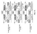
- FIG. 3An exemplary grating-based layout 300 of the SRAM unit cell 200 is shown in FIG. 3 .
- P-type active regions 302 , N-type active regions 306 , and gate lines 304are formed on a regular grating broken up in certain regions, such as, for example, by defining the desired active regions beforehand in the original patterning step, or by removing desired portions of the original grating (see, e.g., FIG. 1 ).
- the P-type active regions 302may be formed by modifying defined active regions in the device by adding a P-type impurity or dopant, such as, for example, boron, of a known concentration level so as to change the conductivity of the material as desired.
- the N-type active regions 306may be formed by modifying defined active regions in the device by adding an N-type impurity or dopant, such as, for example, phosphorus or arsenic, of a known concentration level to change the conductivity of the material as desired.
- the inverters 202 , 204comprising transistor devices P 1 and N 1 , and devices P 2 and N 2 , respectively, are preferably formed by a single gate line stretching across P-type (P+) and N-type (N+) active regions 302 and 306 , respectively.
- Each N-type pull-down transistor device (N 1 or N 2 )shares its drain with a corresponding N-type pass-gate access device (A 1 or A 2 ).
- the two half-cells of SRAM unit cell 200( FIG. 2 ), comprising transistor devices A 1 , N 1 , P 1 or A 2 , N 2 , P 2 , preferably exhibit mirror symmetry in order to allow for cross-coupling of the two inverters.
- the area of the SRAM unit cellwill be dependent on the gate and active region pitch, where the term “pitch” may be defined as a width of the gate or active region plus spacing between adjacent gate or active regions, respectively, in the grating.
- the areais equal to a cell width CW of four times the active region pitch, multiplied by a cell length CL of twice the gate pitch.
- FIG. 4An exemplary connection methodology for the SRAM unit cell 300 is shown in FIG. 4 , which assumes that first layer metal (e.g., metal-1) contact plugs 402 can be used to simultaneously contact gate 406 and active regions 408 to connect the two inverters in a cross-coupled arrangement.
- first layer metale.g., metal-1
- contacts 402are pictured to be substantially the same feature size as the grating lines. However, this need not be the case, as contacts can be larger than the active regions, as long as neighboring shapes do not merge together.
- the layout depicted in FIG. 3has a beta ( ⁇ ) ratio, which may be defined as a ratio of pull-down transistor to pass-gate transistor strengths, of one because the devices are of exactly the same dimensions.
- the relative strength of a given transistoris generally specified in terms of its channel width (W) and channel length (L).
- Wchannel width
- Lchannel length
- additional grating lines corresponding to the pull-down devicescan be electrically connected together in parallel to increase the effective widths (and thus strengths) of the pull-down devices N 1 and N 2 . For example, as shown in the top plan view of FIG.
- each of devices N 1 and N 2may comprise two N-type active area regions 502 , compared to devices P 1 and P 2 , which are each formed of a single P-type active area region 504 .
- This approachmay have a slight area penalty associated therewith, since the cell width in the illustrative embodiment of FIG. 5 will increase to six times the active line pitch, assuming two grating lines are used for the pull-down devices N 1 and N 2 .
- the manufacturability benefitse.g., increased device yield, reduced fabrication costs, etc.
- achieved by using this methodologymay outweigh any increase in area.
- the ⁇ ratioscan alternatively be increased by separately adjusting the threshold voltages of the pass-gate devices A 1 , A 2 and/or pull-down devices N 1 , N 2 as desired, in accordance with another aspect of the invention.
- This methodologycan be accomplished, for instance, through a masked implantation, an example of which is shown in the top plan view of FIG. 6 , which, like the second cut mask described in conjunction with FIG. 1 , requires a lithography step with far less aggressive line dimension control.
- selected regions 602 and 604 of the cellmay be doped to a higher impurity concentration level, so as to increase the threshold voltage of devices (e.g., transistors A 1 and A 2 ) formed in these regions.
- the SRAM unit cell areais determined by the pitch of both the gate and active region gratings.
- the gate pitchis substantially limited by the minimum spacing needed to place a contact between adjacent gate lines.
- the designis very regular, such that every gate shape has contacts above and below.
- Determining the active line pitchis generally not as straightforward, since many different ground rules must be satisfied which makes the active region somewhat irregular.
- the layouts in FIGS. 3 through 6can be used by setting the active pitch equal to the maximum dimension needed to satisfy essentially all IC design rules corresponding to the IC process used.
- an optimum areawould more likely be achieved by reducing the pitch from this maximum value.
- thiswould require that entire grating lines be removed during the two-step patterning process to accommodate design rules including, for example, an N+-to-P+ spacing, gate-contact-to-active spacing, or any alternative technology-dependent design rules that may become important under a given set of process capabilities.
- design rulesincluding, for example, an N+-to-P+ spacing, gate-contact-to-active spacing, or any alternative technology-dependent design rules that may become important under a given set of process capabilities.
- there will exist an optimum point at which the active line pitch and number of grating lines to be removedcan be chosen to satisfy all designs rules while providing a minimum cell area.
- Complete line removalmay not always be a preferred solution, however, because while lithography may not be affected (due to the two-step patterning process), other process steps, such as, as, for example, reactive ion etching and chemical-mechanical planarization, may benefit from a more uniform grating. In such cases, these lines may not need to be completely removed, but merely electrically isolated from other active regions in the device. These electrically isolated active regions may be considered “dummy” active features. As shown in the top plan view of FIG. 8 , these additional dummy active features 802 , 804 essentially do not serve any purpose other than to form a more complete grating.
- the dummy features 802 , 804may add some parasitic capacitance, particularly when running below gate lines, whether through design or through misalignment. However, this additional parasitic capacitance is generally not critical in an SRAM array, as the speed of the cell itself does not typically dominate a critical path in the cell.
- the continuous dummy active region (e.g., 802 or 804 ) running below the inverter gate (e.g., 806 or 808 )may add a significant gate oxide capacitance to the internal nodes (e.g., nodes IN 1 and IN 2 in FIG. 2 ), which, ultimately, may be beneficial for improving soft error immunity.
- the grating-based SRAM unit cell design of the present inventioncan be facilitated by using a stacked three-dimensional (3-D) active layer structure, in which upper device layers can be fabricated from, for example, recrystallized silicon (see e.g., Jung et al., 2004 Symp. on VLSI Technology, the disclosure of which is incorporated by reference herein), wafer bonding techniques, or deposited materials (e.g., carbon nanotubes).
- 3-Dthree-dimensional
- the gate and active region gratings in each of the layerscan be beneficially optimized for, among other things, device area efficiency, on an individual basis.
- An exemplary SRAM unit cell employing multiple stacked active layersis illustrated in the top plan view of FIG. 9 , with each of the active layers 902 , 904 and 906 depicted in separate panels of the figure.
- the vertical ordering of these layersaffects only subsequent interconnection steps and not the cell area.
- the gate and active region pitchis determined predominantly by the minimum spacing needed to place a contact between adjacent gate lines or active region lines, respectively.
- the cell areacan be determined as twice the active region pitch multiplied by twice the gate pitch.
- the fact that the N-type and P-type devices are in different layerseliminates the need for an N+-to-P+ spacing design rule, which results in about a 13 percent reduction in cell area over an SRAM unit cell layout formed in a single dimension.
- each devicecan be individually optimized.
- the gate and active region widthscan be adjusted (at a fixed pitch) for each layer to thereby adjust the cell ⁇ ratio. For example, FIG.
- FIG. 9depicts a cross-sectional view of the exemplary 3-D SRAM unit cell layout shown in FIG. 9 .
- Inter-layer connections made, for example, by way of vias 1000can be achieved using corresponding landing pads 1002 as a potential solution.
- a given landing pad 1002is preferably sized so as to substantially equal a size of the corresponding contact, plus an alignment tolerance with a pitch equal to that of the active grating.
- the conductive layers used to create landing pads 1002can also be used to create additional capacitance on the internal nodes, which increases the stored charge and thus beneficially improves immunity to soft errors, in accordance with another aspect of the invention.
- both gate and active regions of the devicewhich are typically orthogonally disposed relative to one another, be formed on a substantially regular grating. In this manner, IC manufacturability and yield are advantageously improved, thereby reducing the cost of the IC device, particularly when the IC device is comprised of a plurality of repeatable circuit cells.
- gates and active regionsare preferably formed orthogonal to one another, it is similarly contemplated that the gates and active regions in a given circuit may be oriented non-orthogonally relative to one another, such as, for example, diagonally.
- the exemplary layout techniques of the present inventionmay be implemented in an integrated circuit.
- a plurality of identical dieare typically fabricated in a repeated pattern on a surface of a semiconductor wafer.
- Each dieincludes a device described herein, and may include other structures or circuits.
- the individual dieare cut or diced from the wafer, then packaged as an integrated circuit.
- One skilled in the artwould know how to dice wafers and package die to produce integrated circuits. Integrated circuits so manufactured are considered part of this invention.
Landscapes
- Semiconductor Memories (AREA)
- Metal-Oxide And Bipolar Metal-Oxide Semiconductor Integrated Circuits (AREA)
Abstract
Description
This application claims the benefit of priority to U.S. Provisional Application No. 60/633,200, filed on Dec. 3, 2004, the disclosure of which is incorporated by reference herein.
The present invention relates generally to semiconductor devices, and more particularly relates to an integrated circuit (IC) device configured such that both gates and active regions in the device form a regular grating.
Many IC devices, such as, for example, complementary metal-oxide semiconductor (CMOS) devices, are formed comprising a plurality of essentially identical repeated circuit cells, such as, for example, a static random access memory (SRAM) array. As CMOS fabrication technologies advance, SRAM can remain a primary mechanism for affording logic-compatible, high-speed embedded nonvolatile memory, provided corresponding improvements in SRAM cell packing density can be achieved. In order to improve packing density, full scaling of all critical dimensions in the SRAM cell is generally required, which poses significant challenges in process integration, especially in lithography patterning techniques. These challenges include both the resolution of small features as well as the controllability of critical dimensions from device to device, or from wafer to wafer. Such process variations can affect one or more characteristics of the device, including, but not limited to, device threshold voltage, which can severely degrade device yield and/or stability, particularly at reduced power supply voltages. Additionally, it becomes increasing more difficult to fabricate complex geometries in the IC device as dimensions are reduced. Consequently, devices are preferably formed using Manhattan (e.g., x-y) coordinates.
In recent years, there has been a transition from device designs utilizing completely arbitrary pattern sizes and orientations to semi-constrained designs, especially relating to memory design. Semi-constrained designs typically involve maintaining a substantially fixed gate pattern pitch throughout the device. However, gate length is not always fixed. Furthermore, active regions (e.g., source and drain regions) in these devices use varied line dimensions and line spacings, as described, for example, in U.S. Pat. No. 6,534,805 to Jin, the disclosure of which is incorporated by reference herein. Consequently, full scaling of such devices, so as to benefit from shrinking process dimensions, is not easily attainable.
There exists a need, therefore, for a semiconductor design methodology suitable for use, for example, in an SRAM array, which does not suffer from one or more of the above-noted deficiencies associated with conventional semiconductor design approaches.
The present invention, in an illustrative embodiment thereof, provides semiconductor device layout techniques in which both gates and active regions in the device form completely periodic gratings. When device features are comprised of regular patterns based on substantially fixed line widths and spacings, resolution and controllability of critical device dimensions can be advantageously improved. This is due, at least in part, to the fact that patterning techniques do not need to achieve arbitrary shapes, and can thus be optimized for a single line width and space combination. In addition to easing lithography constraints, the techniques of the present invention facilitate the introduction of new high-resolution patterning technologies. Moreover, self-assembly techniques that can precisely define periodic gratings can be more easily employed with a device formed in accordance with the layout techniques of the present invention.
In accordance with one aspect of the invention, a semiconductor device is formed comprising a plurality of repeatable circuit cells connectable to one or more conductors providing at least one of electrical connection to the circuit cells and electrical connection between one or more circuit elements in the cells. Each of the circuit cells are configured having gates and active regions forming a grating, wherein, for a given active layer in the device, a width of each active region is substantially the same relative to one another, a spacing between any two adjacent active regions is substantially the same, a width of each gate is substantially the same relative to one another, and a spacing between any two adjacent gates is substantially the same.
In accordance with another aspect of the invention, in a semiconductor device comprising a plurality of repeatable circuit cells, a method for laying out a given one of the circuit cells includes the steps of: forming a plurality of active regions in the given circuit cell, and forming a plurality of gates in the given circuit cell. The active regions and gates are connectable to one or more conductors providing at least electrical connection to the circuit cell and/or electrical connection between the circuit cell and one or more other circuit cells in the semiconductor device. The active regions form a grating, wherein for a given active layer in the circuit cell a width of each of the active regions is substantially the same relative to one another, and a spacing between any two adjacent active regions is substantially the same. Likewise, the gates form a grating, wherein a width of each of the gates is substantially the same relative to one another, and a spacing between any two adjacent gates is substantially the same.
These and other objects, features and advantages of the present invention will become apparent from the following detailed description of illustrative embodiments thereof, which is to be read in connection with the accompanying drawings.
The present invention will be described herein in the context of an illustrative memory cell for use in an SRAM array comprising a plurality of such memory cells. It should be appreciated, however, that the invention is not limited to this or any particular memory cell configuration. Rather, the invention is more generally applicable to techniques for forming a semiconductor device which may include a plurality of repeated circuit cells, each of the circuit cells being configured such that both gate and active regions in a given layer of the cell form a substantially regular grating. The term “grating” as used herein is intended to refer to a framework of equidistant and parallel lines which may be arranged in a crisscrossed pattern. The term “grating” is often used interchangeably with the term “grid.” In addition to providing increased scalability of the device, thereby beneficially increasing a packing density thereof, the techniques of the present invention described herein can be employed to ease constraints on the lithography process and to improve device yield, thus reducing the overall cost of manufacturing the IC device.
With the advent of 65 nanometer (nm) fabrication technology and beyond, resolution and control of critical dimension variation becomes even more imperative. Since SRAM arrays often utilize perhaps some of the most stringent design rules for IC fabrication, migration to a regular grating-based design can significantly improve packing density and/or chip yield. This is, at least in part, due to the fact that substantially all IC process steps can be optimized for an individual line width and spacing combination rather than for arbitrary shapes. Likewise, with the development of self-assembly techniques that can achieve well-controlled line pitches beyond the capabilities of standard lithography, the grating-based circuit layout technique of the present invention may become particularly important, since most of these techniques can more readily form periodic gratings.
Since a dense circuit layout is typically even more critical in SRAM than in general digital logic or in analog circuitry, it is important to find efficient methods for forming an SRAM unit cell. Since an SRAM circuit often comprises arbitrarily shaped active regions, a two-step patterning process is preferably used to convert a regular grating pattern (original grating) into appropriately interconnected shapes used to represent the arbitrarily shaped active regions in the original design, as shown inFIG. 1 . The term “regular grating” as may be used herein is intended to refer to a pattern comprising a plurality of substantially parallel structures, each structure having the same width and spacing relative to one another throughout the pattern.
As apparent from the figure, the grating pattern may comprise a plurality ofactive regions 102 having substantially equal widths W relative to one another and having substantially equal spacings S between any two adjacent active regions. Rather than defining the desired lengths of the active regions beforehand when the active regions are first formed, which requires more precise control over certain process features (e.g., line width), we can start with an original grating and perform a second patterning step, which can be implemented using far less aggressive technology than needed to form the original grating. Specifically, this second patterning step is preferably used only to removecertain portions
The techniques of the present invention described herein can be applied to silicon-based fabrication techniques, in which patterning is targeted for traditional silicon CMOS. As will be understood by those skilled in the art, these same concepts can be straightforwardly extended to post-silicon technologies, such as, for example, carbon nanotube field-effect transistors (FETs) or other nanowire FETs, in which grating-like arrays of devices may serve as a starting point in the fabrication process.
By way of example only and without loss of generality, theinverters active regions FIG. 2 ), comprising transistor devices A1, N1, P1 or A2, N2, P2, preferably exhibit mirror symmetry in order to allow for cross-coupling of the two inverters. The area of the SRAM unit cell will be dependent on the gate and active region pitch, where the term “pitch” may be defined as a width of the gate or active region plus spacing between adjacent gate or active regions, respectively, in the grating. For theillustrative SRAM cell 300 ofFIG. 3 , the area is equal to a cell width CW of four times the active region pitch, multiplied by a cell length CL of twice the gate pitch.
Depending on metallization options provided by the IC process (e.g., local interconnect, contacts, vias, etc.), interconnection of individual unit cells can be achieved through many different ways, and is thus not a primary focus of the present invention. An exemplary connection methodology for theSRAM unit cell 300 is shown inFIG. 4 , which assumes that first layer metal (e.g., metal-1) contact plugs402 can be used to simultaneously contactgate 406 andactive regions 408 to connect the two inverters in a cross-coupled arrangement. For simplicity,contacts 402 are pictured to be substantially the same feature size as the grating lines. However, this need not be the case, as contacts can be larger than the active regions, as long as neighboring shapes do not merge together.
The layout depicted inFIG. 3 has a beta (β) ratio, which may be defined as a ratio of pull-down transistor to pass-gate transistor strengths, of one because the devices are of exactly the same dimensions. The relative strength of a given transistor is generally specified in terms of its channel width (W) and channel length (L). To improve cell stability during a read access, for example, it is often desirable to increase the β ratio to about two or higher. To achieve this, additional grating lines corresponding to the pull-down devices can be electrically connected together in parallel to increase the effective widths (and thus strengths) of the pull-down devices N1 and N2. For example, as shown in the top plan view ofFIG. 5 , each of devices N1 and N2 may comprise two N-typeactive area regions 502, compared to devices P1 and P2, which are each formed of a single P-typeactive area region 504. This approach may have a slight area penalty associated therewith, since the cell width in the illustrative embodiment ofFIG. 5 will increase to six times the active line pitch, assuming two grating lines are used for the pull-down devices N1 and N2. However, the manufacturability benefits (e.g., increased device yield, reduced fabrication costs, etc.) achieved by using this methodology may outweigh any increase in area.
In order to avoid this area increase, the β ratios can alternatively be increased by separately adjusting the threshold voltages of the pass-gate devices A1, A2 and/or pull-down devices N1, N2 as desired, in accordance with another aspect of the invention. This methodology can be accomplished, for instance, through a masked implantation, an example of which is shown in the top plan view ofFIG. 6 , which, like the second cut mask described in conjunction withFIG. 1 , requires a lithography step with far less aggressive line dimension control. As apparent fromFIG. 6 , selectedregions
In accordance with an important aspect of the present invention, for substantially all of the grating-based layouts discussed herein, the SRAM unit cell area is determined by the pitch of both the gate and active region gratings. In an illustrative embodiment of the invention, the gate pitch is substantially limited by the minimum spacing needed to place a contact between adjacent gate lines. As can be seen inFIG. 3 , the design is very regular, such that every gate shape has contacts above and below. Thus, gate pitch may be determined in accordance with the expression:
Gate pitch=Gate length+Contact size+Contact-to-Gate overlay margin
Gate pitch=Gate length+Contact size+Contact-to-Gate overlay margin
Determining the active line pitch is generally not as straightforward, since many different ground rules must be satisfied which makes the active region somewhat irregular. In the simplest case, the layouts inFIGS. 3 through 6 can be used by setting the active pitch equal to the maximum dimension needed to satisfy essentially all IC design rules corresponding to the IC process used. However, an optimum area would more likely be achieved by reducing the pitch from this maximum value. As shown in the exemplary SRAM unit cell layout ofFIG. 7 , this would require that entire grating lines be removed during the two-step patterning process to accommodate design rules including, for example, an N+-to-P+ spacing, gate-contact-to-active spacing, or any alternative technology-dependent design rules that may become important under a given set of process capabilities. For any given technology, there will exist an optimum point at which the active line pitch and number of grating lines to be removed can be chosen to satisfy all designs rules while providing a minimum cell area.
Complete line removal may not always be a preferred solution, however, because while lithography may not be affected (due to the two-step patterning process), other process steps, such as, as, for example, reactive ion etching and chemical-mechanical planarization, may benefit from a more uniform grating. In such cases, these lines may not need to be completely removed, but merely electrically isolated from other active regions in the device. These electrically isolated active regions may be considered “dummy” active features. As shown in the top plan view ofFIG. 8 , these additional dummyactive features FIG. 2 ), which, ultimately, may be beneficial for improving soft error immunity.
The grating-based SRAM unit cell design of the present invention can be facilitated by using a stacked three-dimensional (3-D) active layer structure, in which upper device layers can be fabricated from, for example, recrystallized silicon (see e.g., Jung et al., 2004 Symp. on VLSI Technology, the disclosure of which is incorporated by reference herein), wafer bonding techniques, or deposited materials (e.g., carbon nanotubes). Because the three device types (e.g., pull-down, pull-up, and pass-gate) can each be formed in separate active layers of the device, each of the layers preferably stacked on top of one another in a substantially vertical dimension, the gate and active region gratings in each of the layers can be beneficially optimized for, among other things, device area efficiency, on an individual basis. An exemplary SRAM unit cell employing multiple stacked active layers is illustrated in the top plan view ofFIG. 9 , with each of theactive layers
The vertical ordering of these layers affects only subsequent interconnection steps and not the cell area. The gate and active region pitch is determined predominantly by the minimum spacing needed to place a contact between adjacent gate lines or active region lines, respectively. The cell area can be determined as twice the active region pitch multiplied by twice the gate pitch. The fact that the N-type and P-type devices are in different layers eliminates the need for an N+-to-P+ spacing design rule, which results in about a 13 percent reduction in cell area over an SRAM unit cell layout formed in a single dimension. Furthermore, because the different device types are formed in different layers, each device can be individually optimized. The gate and active region widths can be adjusted (at a fixed pitch) for each layer to thereby adjust the cell β ratio. For example,FIG. 9 has been drawn such that the pull-down device active region width inlayer 902 and the pass-gate device gate length inlayer 906 have been increased to achieve a larger β ratio compared to standard inverters in the cell. Different threshold voltage adjustment implants can also be easily achieved without separate block masks, since the threedevice layers
The exemplary SRAM unit cell depicted inFIG. 9 assumes an ideal alignment between the three layers. In practice, there may be slight misalignment between the multipleactive layers FIG. 10 depicts a cross-sectional view of the exemplary 3-D SRAM unit cell layout shown inFIG. 9 . Inter-layer connections made, for example, by way ofvias 1000, can be achieved usingcorresponding landing pads 1002 as a potential solution. A givenlanding pad 1002 is preferably sized so as to substantially equal a size of the corresponding contact, plus an alignment tolerance with a pitch equal to that of the active grating. As long as the alignment tolerance is smaller than the grating spacing, cell size should be unaffected. The conductive layers used to createlanding pads 1002 can also be used to create additional capacitance on the internal nodes, which increases the stored charge and thus beneficially improves immunity to soft errors, in accordance with another aspect of the invention.
The techniques of the present invention described herein are not limited to the specific IC layouts or circuits shown in the accompanying figures. Rather, alternative IC layouts may be similarly employed. Regardless of the circuit fabricated, it is an important aspect of the present invention that both gate and active regions of the device, which are typically orthogonally disposed relative to one another, be formed on a substantially regular grating. In this manner, IC manufacturability and yield are advantageously improved, thereby reducing the cost of the IC device, particularly when the IC device is comprised of a plurality of repeatable circuit cells. Although gates and active regions are preferably formed orthogonal to one another, it is similarly contemplated that the gates and active regions in a given circuit may be oriented non-orthogonally relative to one another, such as, for example, diagonally.
The exemplary layout techniques of the present invention may be implemented in an integrated circuit. In forming integrated circuits, a plurality of identical die are typically fabricated in a repeated pattern on a surface of a semiconductor wafer. Each die includes a device described herein, and may include other structures or circuits. The individual die are cut or diced from the wafer, then packaged as an integrated circuit. One skilled in the art would know how to dice wafers and package die to produce integrated circuits. Integrated circuits so manufactured are considered part of this invention.
Although illustrative embodiments of the present invention have been described herein with reference to the accompanying drawings, it is to be understood that the invention is not limited to those precise embodiments, and that various other changes and modifications may be made therein by one skilled in the art without departing from the scope of the appended claims.
Claims (13)
1. A semiconductor device, comprising: a plurality of repeatable circuit cells connectable to one or more conductors providing at least one of electrical connection to the circuit cells and electrical connection between one or more circuit elements in the cells, each of the circuit cells being configured having gates and active regions forming a grid, wherein, for a given active layer in the device, each active region is substantially linear relative to one another and substantially parallel to one another, a width of each active region is substantially the same relative to one another, a spacing between any two adjacent active regions is substantially the same, a width of each gate is substantially the same relative to one another, and a spacing between any two adjacent gates is substantially the same; and
a plurality of active layers, each of the active layers being stacked in a substantially vertical dimension relative to one another when viewed in cross-section, at least a first one of the plurality of circuit cells being formed in a first one of the active layers, and at least a second one of the plurality of circuit cells being formed in a second one of the active layers; and
one or more active regions are broken up in at least one region so as to satisfy specified minimum design rule requirements associated with a fabrication process used to form the device.
2. The device ofclaim 1 , wherein a first portion of at least a first selected active region in at least a given one of the circuit cells is doped with a P-type impurity having a known concentration level to change a conductivity of the first selected active region as desired, and a second portion of at least a second active region in the given circuit cell is doped with an N-type impurity having a known concentration level so as to change a conductivity of the second selected active region as desired.
3. The device ofclaim 1 , wherein at least one of the active regions in at least a given one of the circuit cells is broken up in at least one region.
4. The device ofclaim 1 , wherein a threshold voltage of one or more transistor devices formed in at least one active region grid in at least a given one of the circuit cells is modified compared to another transistor device formed in the given circuit cell.
5. The device ofclaim 1 , wherein at least a given one of the circuit cells comprises an N-type transistor device and a P-type transistor device connected so as to form an inverter, a voltage threshold of at least one of the transistor devices being modified so as to control a ratio of a transconductance of the N-type transistor device relative to a transconductance of the P- type transistor device.
6. The device ofclaim 5 , wherein the ratio of the transconductance of the N-type transistor device relative to the transconductance of the P-type transistor device is greater than or equal to about two.
7. The device ofclaim 1 , wherein at least a given one of the circuit cells comprises an N-type transistor device and a P-type transistor device connected so as to form an inverter, an effective gate width of at least one of the transistor devices being modified by electrically connecting portions of an adjacent active region grid in parallel so as to control a ratio of a transconductance of the N-type transistor device relative to a transconductance of the P-type transistor device.
8. The device ofclaim 1 , wherein the design rule requirements include at least one of a minimum gate-contact-to-active-region-contact spacing and a minimum N-type-active region-to-P-type-active region spacing.
9. The device ofclaim 1 , wherein at least a given one of the circuit cells comprises at least one active region grid which is electrically isolated from any other active region in the given circuit cell.
10. The device ofclaim 1 , wherein the gates and active regions are oriented substantially orthogonal relative to one another.
11. The device ofclaim 1 , wherein the gates and active regions are oriented substantially non-orthogonal relative to one another.
12. The device ofclaim 1 , wherein a first width and a first spacing of active regions in the first active layer is different than a second width and a second spacing of active regions in the second active layer.
13. The device ofclaim 1 , wherein a width and a spacing of active regions in the first active layer is substantially the same as a width and a spacing of active regions in the second active layer.
Priority Applications (3)
| Application Number | Priority Date | Filing Date | Title |
|---|---|---|---|
| US11/065,837US7465973B2 (en) | 2004-12-03 | 2005-02-25 | Integrated circuit having gates and active regions forming a regular grating |
| US11/761,741US7402848B2 (en) | 2004-12-03 | 2007-06-12 | Integrated circuit having gates and active regions forming a regular grating |
| US12/120,878US7791110B2 (en) | 2004-12-03 | 2008-05-15 | Integrated circuit having gates and active regions forming a regular grating |
Applications Claiming Priority (2)
| Application Number | Priority Date | Filing Date | Title |
|---|---|---|---|
| US63320004P | 2004-12-03 | 2004-12-03 | |
| US11/065,837US7465973B2 (en) | 2004-12-03 | 2005-02-25 | Integrated circuit having gates and active regions forming a regular grating |
Related Child Applications (1)
| Application Number | Title | Priority Date | Filing Date |
|---|---|---|---|
| US11/761,741ContinuationUS7402848B2 (en) | 2004-12-03 | 2007-06-12 | Integrated circuit having gates and active regions forming a regular grating |
Publications (2)
| Publication Number | Publication Date |
|---|---|
| US20060121715A1 US20060121715A1 (en) | 2006-06-08 |
| US7465973B2true US7465973B2 (en) | 2008-12-16 |
Family
ID=36574880
Family Applications (3)
| Application Number | Title | Priority Date | Filing Date |
|---|---|---|---|
| US11/065,837Expired - Fee RelatedUS7465973B2 (en) | 2004-12-03 | 2005-02-25 | Integrated circuit having gates and active regions forming a regular grating |
| US11/761,741Expired - Fee RelatedUS7402848B2 (en) | 2004-12-03 | 2007-06-12 | Integrated circuit having gates and active regions forming a regular grating |
| US12/120,878Expired - Fee RelatedUS7791110B2 (en) | 2004-12-03 | 2008-05-15 | Integrated circuit having gates and active regions forming a regular grating |
Family Applications After (2)
| Application Number | Title | Priority Date | Filing Date |
|---|---|---|---|
| US11/761,741Expired - Fee RelatedUS7402848B2 (en) | 2004-12-03 | 2007-06-12 | Integrated circuit having gates and active regions forming a regular grating |
| US12/120,878Expired - Fee RelatedUS7791110B2 (en) | 2004-12-03 | 2008-05-15 | Integrated circuit having gates and active regions forming a regular grating |
Country Status (1)
| Country | Link |
|---|---|
| US (3) | US7465973B2 (en) |
Cited By (35)
| Publication number | Priority date | Publication date | Assignee | Title |
|---|---|---|---|---|
| US7842975B2 (en) | 2006-03-09 | 2010-11-30 | Tela Innovations, Inc. | Dynamic array architecture |
| US7888705B2 (en) | 2007-08-02 | 2011-02-15 | Tela Innovations, Inc. | Methods for defining dynamic array section with manufacturing assurance halo and apparatus implementing the same |
| US7932545B2 (en) | 2006-03-09 | 2011-04-26 | Tela Innovations, Inc. | Semiconductor device and associated layouts including gate electrode level region having arrangement of six linear conductive segments with side-to-side spacing less than 360 nanometers |
| US7939443B2 (en) | 2008-03-27 | 2011-05-10 | Tela Innovations, Inc. | Methods for multi-wire routing and apparatus implementing same |
| US7943967B2 (en) | 2006-03-09 | 2011-05-17 | Tela Innovations, Inc. | Semiconductor device and associated layouts including diffusion contact placement restriction based on relation to linear conductive segments |
| US7956421B2 (en) | 2008-03-13 | 2011-06-07 | Tela Innovations, Inc. | Cross-coupled transistor layouts in restricted gate level layout architecture |
| US7969199B1 (en) | 2010-05-10 | 2011-06-28 | Pdf Solutions, Inc. | Pattern controlled IC layout |
| US20110156148A1 (en)* | 2009-12-30 | 2011-06-30 | Taiwan Semiconductor Manufacturing Co., Ltd. | Semiconductor device and method for making the same using semiconductor fin density design rules |
| US7979829B2 (en) | 2007-02-20 | 2011-07-12 | Tela Innovations, Inc. | Integrated circuit cell library with cell-level process compensation technique (PCT) application and associated methods |
| US7994545B2 (en) | 2007-10-26 | 2011-08-09 | Tela Innovations, Inc. | Methods, structures, and designs for self-aligning local interconnects used in integrated circuits |
| US8214778B2 (en) | 2007-08-02 | 2012-07-03 | Tela Innovations, Inc. | Methods for cell phasing and placement in dynamic array architecture and implementation of the same |
| US8225239B2 (en) | 2006-03-09 | 2012-07-17 | Tela Innovations, Inc. | Methods for defining and utilizing sub-resolution features in linear topology |
| US8225261B2 (en) | 2006-03-09 | 2012-07-17 | Tela Innovations, Inc. | Methods for defining contact grid in dynamic array architecture |
| US8245180B2 (en) | 2006-03-09 | 2012-08-14 | Tela Innovations, Inc. | Methods for defining and using co-optimized nanopatterns for integrated circuit design and apparatus implementing same |
| US8247846B2 (en) | 2006-03-09 | 2012-08-21 | Tela Innovations, Inc. | Oversized contacts and vias in semiconductor chip defined by linearly constrained topology |
| US8286107B2 (en) | 2007-02-20 | 2012-10-09 | Tela Innovations, Inc. | Methods and systems for process compensation technique acceleration |
| US8448102B2 (en) | 2006-03-09 | 2013-05-21 | Tela Innovations, Inc. | Optimizing layout of irregular structures in regular layout context |
| US8453094B2 (en) | 2008-01-31 | 2013-05-28 | Tela Innovations, Inc. | Enforcement of semiconductor structure regularity for localized transistors and interconnect |
| US8541879B2 (en) | 2007-12-13 | 2013-09-24 | Tela Innovations, Inc. | Super-self-aligned contacts and method for making the same |
| US8653857B2 (en) | 2006-03-09 | 2014-02-18 | Tela Innovations, Inc. | Circuitry and layouts for XOR and XNOR logic |
| US8658542B2 (en) | 2006-03-09 | 2014-02-25 | Tela Innovations, Inc. | Coarse grid design methods and structures |
| US8661392B2 (en) | 2009-10-13 | 2014-02-25 | Tela Innovations, Inc. | Methods for cell boundary encroachment and layouts implementing the Same |
| US8667443B2 (en) | 2007-03-05 | 2014-03-04 | Tela Innovations, Inc. | Integrated circuit cell library for multiple patterning |
| US8759179B2 (en)* | 2011-04-29 | 2014-06-24 | Semiconductor Manufacturing International (Shanghai) Corporation | Method of forming gate pattern and semiconductor device |
| US8839175B2 (en) | 2006-03-09 | 2014-09-16 | Tela Innovations, Inc. | Scalable meta-data objects |
| US8863063B2 (en) | 2009-05-06 | 2014-10-14 | Tela Innovations, Inc. | Finfet transistor circuit |
| US9035359B2 (en) | 2006-03-09 | 2015-05-19 | Tela Innovations, Inc. | Semiconductor chip including region including linear-shaped conductive structures forming gate electrodes and having electrical connection areas arranged relative to inner region between transistors of different types and associated methods |
| US9122832B2 (en) | 2008-08-01 | 2015-09-01 | Tela Innovations, Inc. | Methods for controlling microloading variation in semiconductor wafer layout and fabrication |
| US9159627B2 (en) | 2010-11-12 | 2015-10-13 | Tela Innovations, Inc. | Methods for linewidth modification and apparatus implementing the same |
| US9230910B2 (en) | 2006-03-09 | 2016-01-05 | Tela Innovations, Inc. | Oversized contacts and vias in layout defined by linearly constrained topology |
| US9563733B2 (en) | 2009-05-06 | 2017-02-07 | Tela Innovations, Inc. | Cell circuit and layout with linear finfet structures |
| US9570591B1 (en)* | 2015-09-24 | 2017-02-14 | International Business Machines Corporation | Forming semiconductor device with close ground rules |
| US10109637B1 (en)* | 2017-12-28 | 2018-10-23 | Globalfoundries Inc. | Cross couple structure for vertical transistors |
| US10497692B2 (en) | 2017-08-29 | 2019-12-03 | Globalfoundries Inc. | SRAM structure with alternate gate pitches |
| US20200365589A1 (en)* | 2019-05-17 | 2020-11-19 | Taiwan Semiconductor Manufacturing Co., Ltd. | Integrated Circuit Device and Method of Forming the Same |
Families Citing this family (30)
| Publication number | Priority date | Publication date | Assignee | Title |
|---|---|---|---|---|
| US7302651B2 (en)* | 2004-10-29 | 2007-11-27 | International Business Machines Corporation | Technology migration for integrated circuits with radical design restrictions |
| US7343581B2 (en)* | 2005-06-27 | 2008-03-11 | Tela Innovations, Inc. | Methods for creating primitive constructed standard cells |
| CN1893085A (en)* | 2005-07-07 | 2007-01-10 | 松下电器产业株式会社 | Semiconductor device and method for fabricating the same |
| US7590968B1 (en) | 2006-03-01 | 2009-09-15 | Tela Innovations, Inc. | Methods for risk-informed chip layout generation |
| US7586800B1 (en) | 2006-08-08 | 2009-09-08 | Tela Innovations, Inc. | Memory timing apparatus and associated methods |
| JP2009130210A (en)* | 2007-11-26 | 2009-06-11 | Toshiba Corp | Semiconductor device |
| KR101387689B1 (en) | 2008-01-25 | 2014-04-22 | 삼성전자주식회사 | Semiconductor device |
| FR2932005B1 (en)* | 2008-06-02 | 2011-04-01 | Commissariat Energie Atomique | INTEGRATED TRANSISTOR CIRCUIT IN THREE DIMENSIONS HAVING DYNAMICALLY ADJUSTABLE VT THRESHOLD VOLTAGE |
| JP5147654B2 (en)* | 2008-11-18 | 2013-02-20 | パナソニック株式会社 | Semiconductor device |
| US8198655B1 (en)* | 2009-04-27 | 2012-06-12 | Carnegie Mellon University | Regular pattern arrays for memory and logic on a semiconductor substrate |
| US8084308B2 (en)* | 2009-05-21 | 2011-12-27 | International Business Machines Corporation | Single gate inverter nanowire mesh |
| US8216902B2 (en)* | 2009-08-06 | 2012-07-10 | International Business Machines Corporation | Nanomesh SRAM cell |
| US8258572B2 (en)* | 2009-12-07 | 2012-09-04 | Taiwan Semiconductor Manufacturing Company, Ltd. | SRAM structure with FinFETs having multiple fins |
| US9220180B2 (en)* | 2010-12-09 | 2015-12-22 | Richard Anthony Dunn, JR. | System and methods for scalable parallel data processing and process control |
| KR20110104767A (en)* | 2010-03-17 | 2011-09-23 | 주식회사 하이닉스반도체 | Method for manufacturing semiconductor device |
| US8324940B2 (en) | 2010-04-13 | 2012-12-04 | International Business Machines Corporation | Nanowire circuits in matched devices |
| JP5744564B2 (en)* | 2011-02-25 | 2015-07-08 | キヤノン株式会社 | Drawing apparatus, drawing method, and article manufacturing method |
| JP5690683B2 (en)* | 2011-07-22 | 2015-03-25 | ルネサスエレクトロニクス株式会社 | Semiconductor device |
| US9236267B2 (en)* | 2012-02-09 | 2016-01-12 | Taiwan Semiconductor Manufacturing Company, Ltd. | Cut-mask patterning process for fin-like field effect transistor (FinFET) device |
| US8736061B2 (en)* | 2012-06-07 | 2014-05-27 | GlobalFoundries, Inc. | Integrated circuits having a continuous active area and methods for fabricating same |
| US8823178B2 (en)* | 2012-09-14 | 2014-09-02 | Globalfoundries Inc. | Bit cell with double patterned metal layer structures |
| US8921197B2 (en)* | 2012-09-14 | 2014-12-30 | GlobalFoundries, Inc. | Integrated circuits with SRAM cells having additional read stacks and methods for their fabrication |
| US9418196B2 (en)* | 2013-03-15 | 2016-08-16 | Taiwan Semiconductor Manufacturing Company, Ltd. | Layout optimization for integrated circuit design |
| US9209195B2 (en)* | 2013-05-01 | 2015-12-08 | Texas Instruments Incorporated | SRAM well-tie with an uninterrupted grated first poly and first contact patterns in a bit cell array |
| CN105719688B (en)* | 2014-12-04 | 2019-03-29 | 中芯国际集成电路制造(上海)有限公司 | SRAM memory and the method for forming SRAM memory |
| US9391080B1 (en) | 2015-04-28 | 2016-07-12 | Globalfoundries Inc. | Memory bit cell for reduced layout area |
| KR102415328B1 (en)* | 2015-12-03 | 2022-06-30 | 삼성전자주식회사 | Static Random Access Memory (SRAM) device for improving electrical characteristics, and logic device including the same |
| WO2017145906A1 (en)* | 2016-02-25 | 2017-08-31 | 株式会社ソシオネクスト | Semiconductor integrated circuit device |
| US10515969B2 (en) | 2016-11-17 | 2019-12-24 | Taiwan Semiconductor Manufacturing Co., Ltd. | Semiconductor device and manufacturing method thereof |
| DE102021105450B4 (en)* | 2020-05-28 | 2023-03-02 | Taiwan Semiconductor Manufacturing Co., Ltd. | Integrated circuit device, system and method |
Citations (9)
| Publication number | Priority date | Publication date | Assignee | Title |
|---|---|---|---|---|
| US5287304A (en)* | 1990-12-31 | 1994-02-15 | Texas Instruments Incorporated | Memory cell circuit and array |
| US5359226A (en)* | 1993-02-02 | 1994-10-25 | Paradigm Technology, Inc. | Static memory with self aligned contacts and split word lines |
| US5612552A (en)* | 1994-03-31 | 1997-03-18 | Lsi Logic Corporation | Multilevel gate array integrated circuit structure with perpendicular access to all active device regions |
| US5742086A (en)* | 1994-11-02 | 1998-04-21 | Lsi Logic Corporation | Hexagonal DRAM array |
| US6271063B1 (en)* | 1997-06-24 | 2001-08-07 | Stmicroelectronics, Inc. | Method of making an SRAM cell and structure |
| US6534805B1 (en) | 2001-04-09 | 2003-03-18 | Cypress Semiconductor Corp. | SRAM cell design |
| US6573549B1 (en)* | 2002-06-21 | 2003-06-03 | Texas Instruments Incorporated | Dynamic threshold voltage 6T SRAM cell |
| US6812534B2 (en)* | 2002-09-10 | 2004-11-02 | Renesas Technology Corp. | Static semiconductor memory device |
| US20050023633A1 (en)* | 2003-08-01 | 2005-02-03 | Yee-Chia Yeo | Semiconductor-on-insulator SRAM configured using partially-depleted and fully-depleted transistors |
Family Cites Families (1)
| Publication number | Priority date | Publication date | Assignee | Title |
|---|---|---|---|---|
| US6534405B1 (en)* | 2001-10-01 | 2003-03-18 | Taiwan Semiconductor Manufacturing Company | Method of forming a MOSFET device featuring a dual salicide process |
- 2005
- 2005-02-25USUS11/065,837patent/US7465973B2/ennot_activeExpired - Fee Related
- 2007
- 2007-06-12USUS11/761,741patent/US7402848B2/ennot_activeExpired - Fee Related
- 2008
- 2008-05-15USUS12/120,878patent/US7791110B2/ennot_activeExpired - Fee Related
Patent Citations (9)
| Publication number | Priority date | Publication date | Assignee | Title |
|---|---|---|---|---|
| US5287304A (en)* | 1990-12-31 | 1994-02-15 | Texas Instruments Incorporated | Memory cell circuit and array |
| US5359226A (en)* | 1993-02-02 | 1994-10-25 | Paradigm Technology, Inc. | Static memory with self aligned contacts and split word lines |
| US5612552A (en)* | 1994-03-31 | 1997-03-18 | Lsi Logic Corporation | Multilevel gate array integrated circuit structure with perpendicular access to all active device regions |
| US5742086A (en)* | 1994-11-02 | 1998-04-21 | Lsi Logic Corporation | Hexagonal DRAM array |
| US6271063B1 (en)* | 1997-06-24 | 2001-08-07 | Stmicroelectronics, Inc. | Method of making an SRAM cell and structure |
| US6534805B1 (en) | 2001-04-09 | 2003-03-18 | Cypress Semiconductor Corp. | SRAM cell design |
| US6573549B1 (en)* | 2002-06-21 | 2003-06-03 | Texas Instruments Incorporated | Dynamic threshold voltage 6T SRAM cell |
| US6812534B2 (en)* | 2002-09-10 | 2004-11-02 | Renesas Technology Corp. | Static semiconductor memory device |
| US20050023633A1 (en)* | 2003-08-01 | 2005-02-03 | Yee-Chia Yeo | Semiconductor-on-insulator SRAM configured using partially-depleted and fully-depleted transistors |
Non-Patent Citations (1)
| Title |
|---|
| M. Ishida et al., "A Novel 6T-SRAM Cell Technology Designed with Rectangular Patterns Scalable beyond 0.18 mum Generation and Desirable for Ultra High Speed Operation," IEEE, 4 pages, 1998. |
Cited By (206)
| Publication number | Priority date | Publication date | Assignee | Title |
|---|---|---|---|---|
| US9240413B2 (en) | 2006-03-09 | 2016-01-19 | Tela Innovations, Inc. | Methods, structures, and designs for self-aligning local interconnects used in integrated circuits |
| US7842975B2 (en) | 2006-03-09 | 2010-11-30 | Tela Innovations, Inc. | Dynamic array architecture |
| US10230377B2 (en) | 2006-03-09 | 2019-03-12 | Tela Innovations, Inc. | Circuitry and layouts for XOR and XNOR logic |
| US7906801B2 (en) | 2006-03-09 | 2011-03-15 | Tela Innovations, Inc. | Semiconductor device and associated layouts having transistors formed from six linear conductive segments with intervening diffusion contact restrictions |
| US7910959B2 (en) | 2006-03-09 | 2011-03-22 | Tela Innovations, Inc. | Semiconductor device and associated layouts having transistors formed from six linear conductive segments with gate electrode connection through single interconnect level |
| US7910958B2 (en) | 2006-03-09 | 2011-03-22 | Tela Innovations, Inc. | Semiconductor device and associated layouts having transistors formed from linear conductive segment with non-active neighboring linear conductive segment |
| US10217763B2 (en) | 2006-03-09 | 2019-02-26 | Tela Innovations, Inc. | Semiconductor chip having region including gate electrode features of rectangular shape on gate horizontal grid and first-metal structures of rectangular shape on at least eight first-metal gridlines of first-metal vertical grid |
| US7923757B2 (en) | 2006-03-09 | 2011-04-12 | Tela Innovations, Inc. | Semiconductor device and associated layouts having linear shaped gate electrodes defined along at least five adjacent gate electrode tracks of equal pitch with gate electrode connection through single interconnect level |
| US7932544B2 (en) | 2006-03-09 | 2011-04-26 | Tela Innovations, Inc. | Semiconductor device and associated layouts including linear conductive segments having non-gate extension portions |
| US7932545B2 (en) | 2006-03-09 | 2011-04-26 | Tela Innovations, Inc. | Semiconductor device and associated layouts including gate electrode level region having arrangement of six linear conductive segments with side-to-side spacing less than 360 nanometers |
| US10186523B2 (en) | 2006-03-09 | 2019-01-22 | Tela Innovations, Inc. | Semiconductor chip having region including gate electrode features formed in part from rectangular layout shapes on gate horizontal grid and first-metal structures formed in part from rectangular layout shapes on at least eight first-metal gridlines of first-metal vertical grid |
| US7943967B2 (en) | 2006-03-09 | 2011-05-17 | Tela Innovations, Inc. | Semiconductor device and associated layouts including diffusion contact placement restriction based on relation to linear conductive segments |
| US7943966B2 (en) | 2006-03-09 | 2011-05-17 | Tela Innovations, Inc. | Integrated circuit and associated layout with gate electrode level portion including at least two complimentary transistor forming linear conductive segments and at least one non-gate linear conductive segment |
| US7948012B2 (en) | 2006-03-09 | 2011-05-24 | Tela Innovations, Inc. | Semiconductor device having 1965 nm gate electrode level region including at least four active linear conductive segments and at least one non-gate linear conductive segment |
| US7948013B2 (en) | 2006-03-09 | 2011-05-24 | Tela Innovations, Inc. | Semiconductor device and associated layouts having linear shaped gate electrodes defined along at least five adjacent gate electrode tracks of equal pitch |
| US7952119B2 (en) | 2006-03-09 | 2011-05-31 | Tela Innovations, Inc. | Semiconductor device and associated layout having three or more linear-shaped gate electrode level conductive segments of both equal length and equal pitch |
| US10141334B2 (en) | 2006-03-09 | 2018-11-27 | Tela Innovations, Inc. | Semiconductor chip including region having rectangular-shaped gate structures and first-metal structures |
| US10141335B2 (en) | 2006-03-09 | 2018-11-27 | Tela Innovations, Inc. | Semiconductor CIP including region having rectangular-shaped gate structures and first metal structures |
| US9917056B2 (en) | 2006-03-09 | 2018-03-13 | Tela Innovations, Inc. | Coarse grid design methods and structures |
| US9905576B2 (en) | 2006-03-09 | 2018-02-27 | Tela Innovations, Inc. | Semiconductor chip including region having rectangular-shaped gate structures and first metal structures |
| US7989848B2 (en) | 2006-03-09 | 2011-08-02 | Tela Innovations, Inc. | Semiconductor device having at least four side-by-side electrodes of equal length and equal pitch with at least two transistor connections to power or ground |
| US7989847B2 (en) | 2006-03-09 | 2011-08-02 | Tela Innovations, Inc. | Semiconductor device having linear-shaped gate electrodes of different transistor types with uniformity extending portions of different lengths |
| US9859277B2 (en) | 2006-03-09 | 2018-01-02 | Tela Innovations, Inc. | Methods, structures, and designs for self-aligning local interconnects used in integrated circuits |
| US9754878B2 (en) | 2006-03-09 | 2017-09-05 | Tela Innovations, Inc. | Semiconductor chip including a chip level based on a layout that includes both regular and irregular wires |
| US8022441B2 (en) | 2006-03-09 | 2011-09-20 | Tela Innovations, Inc. | Semiconductor device and associated layouts having transistors formed from six linear conductive segments with gate electrode-to-gate electrode connection through single interconnect level and common node connection through different interconnect level |
| US8030689B2 (en) | 2006-03-09 | 2011-10-04 | Tela Innovations, Inc. | Integrated circuit device and associated layout including separated diffusion regions of different type each having four gate electrodes with each of two complementary gate electrode pairs formed from respective linear conductive segment |
| US8035133B2 (en) | 2006-03-09 | 2011-10-11 | Tela Innovations, Inc. | Semiconductor device having two pairs of transistors of different types formed from shared linear-shaped conductive features with intervening transistors of common type on equal pitch |
| US8058671B2 (en) | 2006-03-09 | 2011-11-15 | Tela Innovations, Inc. | Semiconductor device having at least three linear-shaped electrode level conductive features of equal length positioned side-by-side at equal pitch |
| US9741719B2 (en) | 2006-03-09 | 2017-08-22 | Tela Innovations, Inc. | Methods, structures, and designs for self-aligning local interconnects used in integrated circuits |
| US8072003B2 (en) | 2006-03-09 | 2011-12-06 | Tela Innovations, Inc. | Integrated circuit device and associated layout including two pairs of co-aligned complementary gate electrodes with offset gate contact structures |
| US8089104B2 (en) | 2006-03-09 | 2012-01-03 | Tela Innovations, Inc. | Integrated circuit with gate electrode level region including multiple linear-shaped conductive structures forming gate electrodes of transistors and including uniformity extending portions of different size |
| US8089103B2 (en) | 2006-03-09 | 2012-01-03 | Tela Innovations, Inc. | Integrated circuit device with gate level region including at least three linear-shaped conductive segments having offset line ends and forming three transistors of first type and one transistor of second type |
| US8089102B2 (en) | 2006-03-09 | 2012-01-03 | Tela Innovations, Inc. | Method for fabricating integrated circuit having three or more linear-shaped gate electrode level conductive segments of both equal length and equal pitch |
| US8088680B2 (en) | 2006-03-09 | 2012-01-03 | Tela Innovations, Inc. | Method for fabricating integrated circuit having at least three linear-shaped gate electrode level conductive features of equal length positioned side-by-side at equal pitch |
| US8088682B2 (en) | 2006-03-09 | 2012-01-03 | Tela Innovations, Inc. | Method for fabricating integrated circuit with gate electrode level region including two side-by-side ones of at least three linear-shaped conductive structures electrically connected to each other through non-gate level |
| US8089098B2 (en) | 2006-03-09 | 2012-01-03 | Tela Innovations, Inc. | Integrated circuit device and associated layout including linear gate electrodes of different transistor types next to linear-shaped non-gate conductive segment |
| US8088681B2 (en) | 2006-03-09 | 2012-01-03 | Tela Innovations, Inc. | Method for fabricating integrated circuit including separated diffusion regions of different type each having four gate electrodes with each of two complementary gate electrode pairs formed from respective linear condcutive segment |
| US8089101B2 (en) | 2006-03-09 | 2012-01-03 | Tela Innovations, Inc. | Integrated circuit device with gate electrode level region including two side-by-side ones of at least three linear-shaped conductive structures electrically connected to each other through non-gate level |
| US8088679B2 (en) | 2006-03-09 | 2012-01-03 | Tela Innovations, Inc. | Method for fabricating integrated circuit with gate electrode level portion including at least two complementary transistor forming linear conductive segments and at least one non-gate linear conductive segment |
| US8089099B2 (en) | 2006-03-09 | 2012-01-03 | Tela Innovations, Inc, | Integrated circuit device and associated layout including gate electrode level region of 965 NM radius with linear-shaped conductive segments on fixed pitch |
| US8089100B2 (en) | 2006-03-09 | 2012-01-03 | Tela Innovations, Inc. | Integrated circuit with gate electrode level region including at least four linear-shaped conductive structures forming gate electrodes of transistors and including extending portions of at least two different sizes |
| US8101975B2 (en) | 2006-03-09 | 2012-01-24 | Tela Innovations, Inc. | Integrated circuit device with gate level region including non-gate linear conductive segment positioned within 965 nanometers of four transistors of first type and four transistors of second type |
| US8110854B2 (en) | 2006-03-09 | 2012-02-07 | Tela Innovations, Inc. | Integrated circuit device with linearly defined gate electrode level region and shared diffusion region of first type connected to shared diffusion region of second type through at least two interconnect levels |
| US8129754B2 (en) | 2006-03-09 | 2012-03-06 | Tela Innovations, Inc. | Integrated circuit with gate electrode level including at least six linear-shaped conductive structures forming gate electrodes of transisters with at least one pair of linear-shaped conductive structures having offset ends |
| US8129752B2 (en) | 2006-03-09 | 2012-03-06 | Tela Innovations, Inc. | Integrated circuit including a linear-shaped conductive structure forming one gate electrode and having length greater than or equal to one-half the length of linear-shaped conductive structure forming two gate electrodes |
| US8129757B2 (en) | 2006-03-09 | 2012-03-06 | Tela Innovations, Inc. | Integrated circuit including at least six linear-shaped conductive structive structures at equal pitch including at least two linear-shaped conductive structures having non-gate portions of different length |
| US8129750B2 (en) | 2006-03-09 | 2012-03-06 | Tela Innovations, Inc. | Integrated circuit including at least six linear-shaped conductive structures forming gate electrodes of transistors with at least two linear-shaped conductive structures of different length |
| US8129819B2 (en) | 2006-03-09 | 2012-03-06 | Tela Innovations, Inc. | Method of fabricating integrated circuit including at least six linear-shaped conductive structures at equal pitch including at least two linear-shaped conductive structures having non-gate portions of different length |
| US8129753B2 (en) | 2006-03-09 | 2012-03-06 | Tela Innovations, Inc. | Integrated circuit including gate electrode level region including at least seven linear-shaped conductive structures of equal length positioned at equal pitch with at least two linear-shaped conductive structures each forming one transistor and having extending portion sized greater than gate portion |
| US8129756B2 (en) | 2006-03-09 | 2012-03-06 | Tela Innovations, Inc. | Integrated circuit including at least six linear-shaped conductive structures forming gate electrodes of transistors with at least two different extension distances beyond conductive contacting structures |
| US8129751B2 (en) | 2006-03-09 | 2012-03-06 | Tela Innovations, Inc. | Integrated circuit including at least six linear-shaped conductive structures forming gate electrodes and including four conductive contacting structures having at least two different connection distances |
| US8129755B2 (en) | 2006-03-09 | 2012-03-06 | Tela Innovations, Inc. | Integrated circuit with gate electrode level including at least four linear-shaped conductive structures of equal length and equal pitch with linear-shaped conductive structure forming one transistor |
| US8134184B2 (en) | 2006-03-09 | 2012-03-13 | Tela Innovations, Inc. | Integrated circuit having gate electrode level region including at least four linear-shaped conductive structures with some outer-contacted linear-shaped conductive structures having larger outer extending portion than inner extending portion |
| US8134183B2 (en) | 2006-03-09 | 2012-03-13 | Tela Innovations, Inc. | Integrated circuit including linear-shaped conductive structures that have gate portions and extending portions of different size |
| US8134186B2 (en) | 2006-03-09 | 2012-03-13 | Tela Innovations, Inc. | Integrated circuit including at least three linear-shaped conductive structures at equal pitch including linear-shaped conductive structure having non-gate portion length greater than gate portion length |
| US8134185B2 (en) | 2006-03-09 | 2012-03-13 | Tela Innovations, Inc. | Integrated circuit having gate electrode level region including at least seven linear-shaped conductive structures at equal pitch including linear-shaped conductive structure forming transistors of two different types and at least three linear-shaped conductive structures having aligned ends |
| US8138525B2 (en) | 2006-03-09 | 2012-03-20 | Tela Innovations, Inc. | Integrated circuit including at least three linear-shaped conductive structures of different length each forming gate of different transistor |
| US8198656B2 (en) | 2006-03-09 | 2012-06-12 | Tela Innovations, Inc. | Integrated circuit including gate electrode level region including at least four linear-shaped conductive structures of equal length having aligned ends and positioned at equal pitch and forming multiple gate electrodes of transistors of different type |
| US8207053B2 (en) | 2006-03-09 | 2012-06-26 | Tela Innovations, Inc. | Electrodes of transistors with at least two linear-shaped conductive structures of different length |
| US9711495B2 (en) | 2006-03-09 | 2017-07-18 | Tela Innovations, Inc. | Oversized contacts and vias in layout defined by linearly constrained topology |
| US8217428B2 (en) | 2006-03-09 | 2012-07-10 | Tela Innovations, Inc. | Integrated circuit including gate electrode level region including at least three linear-shaped conductive structures of equal length having aligned ends and positioned at equal pitch and forming multiple gate electrodes of transistors of different type |
| US8225239B2 (en) | 2006-03-09 | 2012-07-17 | Tela Innovations, Inc. | Methods for defining and utilizing sub-resolution features in linear topology |
| US8225261B2 (en) | 2006-03-09 | 2012-07-17 | Tela Innovations, Inc. | Methods for defining contact grid in dynamic array architecture |
| US8245180B2 (en) | 2006-03-09 | 2012-08-14 | Tela Innovations, Inc. | Methods for defining and using co-optimized nanopatterns for integrated circuit design and apparatus implementing same |
| US8247846B2 (en) | 2006-03-09 | 2012-08-21 | Tela Innovations, Inc. | Oversized contacts and vias in semiconductor chip defined by linearly constrained topology |
| US8253172B2 (en) | 2006-03-09 | 2012-08-28 | Tela Innovations, Inc. | Semiconductor device with linearly restricted gate level region including four serially connected transistors of first type and four serially connected transistors of second type separated by non-diffusion region |
| US8253173B2 (en) | 2006-03-09 | 2012-08-28 | Tela Innovations, Inc. | Semiconductor device with gate level including four transistors of first type and four transistors of second type separated by non-diffusion region and having at least two gate contacts positioned outside separating non-diffusion region |
| US8258549B2 (en) | 2006-03-09 | 2012-09-04 | Tela Innovations, Inc. | Semiconductor device including two transistors of first type having gates formed by conductors of different length respectively aligned with two transistors of second type having gates formed by conductors of different length |
| US8258548B2 (en) | 2006-03-09 | 2012-09-04 | Tela Innovations, Inc. | Semiconductor device with gate level including four transistors of first type and four transistors of second type separated by non-diffusion region with restricted gate contact placement over separating non-diffusion region |
| US8258551B2 (en) | 2006-03-09 | 2012-09-04 | Tela Innovations, Inc. | Semiconductor device with gate level including transistors of first type and transistors of second type with corresponding gate contact placement restriction |
| US9673825B2 (en) | 2006-03-09 | 2017-06-06 | Tela Innovations, Inc. | Circuitry and layouts for XOR and XNOR logic |
| US8258547B2 (en) | 2006-03-09 | 2012-09-04 | Tela Innovations, Inc. | Semiconductor device with linearly restricted gate level region including two transistors of first type and two transistors of second type with offset gate contacts |
| US8258552B2 (en) | 2006-03-09 | 2012-09-04 | Tela Innovations, Inc. | Semiconductor device including at least six transistor forming linear shapes with at least two transistor forming linear shapes having offset ends |
| US8258550B2 (en) | 2006-03-09 | 2012-09-04 | Tela Innovations, Inc. | Semiconductor device including at least six transistor forming linear shapes including at least two transistor forming linear shapes having different extension distances beyond gate contact |
| US8653857B2 (en) | 2006-03-09 | 2014-02-18 | Tela Innovations, Inc. | Circuitry and layouts for XOR and XNOR logic |
| US8264007B2 (en) | 2006-03-09 | 2012-09-11 | Tela Innovations, Inc. | Semiconductor device including at least six transistor forming linear shapes including at least two different gate contact connection distances |
| US9589091B2 (en) | 2006-03-09 | 2017-03-07 | Tela Innovations, Inc. | Scalable meta-data objects |
| US8264008B2 (en) | 2006-03-09 | 2012-09-11 | Tela Innovations, Inc. | Semiconductor device including transistor forming linear shapes including gate portions and extending portions of different size |
| US8264009B2 (en) | 2006-03-09 | 2012-09-11 | Tela Innovations, Inc. | Semiconductor device with linearly restricted gate level region including four transistors of first type and four transistors of second type with gate defining shapes of different length |
| US9443947B2 (en) | 2006-03-09 | 2016-09-13 | Tela Innovations, Inc. | Semiconductor chip including region having integrated circuit transistor gate electrodes formed by various conductive structures of specified shape and position and method for manufacturing the same |
| US9425272B2 (en) | 2006-03-09 | 2016-08-23 | Tela Innovations, Inc. | Semiconductor chip including integrated circuit including four transistors of first transistor type and four transistors of second transistor type with electrical connections between various transistors and methods for manufacturing the same |
| US9425145B2 (en) | 2006-03-09 | 2016-08-23 | Tela Innovations, Inc. | Oversized contacts and vias in layout defined by linearly constrained topology |
| US9425273B2 (en) | 2006-03-09 | 2016-08-23 | Tela Innovations, Inc. | Semiconductor chip including integrated circuit including at least five gate level conductive structures having particular spatial and electrical relationship and method for manufacturing the same |
| US9336344B2 (en) | 2006-03-09 | 2016-05-10 | Tela Innovations, Inc. | Coarse grid design methods and structures |
| US9230910B2 (en) | 2006-03-09 | 2016-01-05 | Tela Innovations, Inc. | Oversized contacts and vias in layout defined by linearly constrained topology |
| US9035359B2 (en) | 2006-03-09 | 2015-05-19 | Tela Innovations, Inc. | Semiconductor chip including region including linear-shaped conductive structures forming gate electrodes and having electrical connection areas arranged relative to inner region between transistors of different types and associated methods |
| US8436400B2 (en) | 2006-03-09 | 2013-05-07 | Tela Innovations, Inc. | Semiconductor device with gate level including gate electrode conductors for transistors of first type and transistors of second type with some gate electrode conductors of different length |
| US8448102B2 (en) | 2006-03-09 | 2013-05-21 | Tela Innovations, Inc. | Optimizing layout of irregular structures in regular layout context |
| US9009641B2 (en) | 2006-03-09 | 2015-04-14 | Tela Innovations, Inc. | Circuits with linear finfet structures |
| US8952425B2 (en) | 2006-03-09 | 2015-02-10 | Tela Innovations, Inc. | Integrated circuit including at least four linear-shaped conductive structures having extending portions of different length |
| US8658542B2 (en) | 2006-03-09 | 2014-02-25 | Tela Innovations, Inc. | Coarse grid design methods and structures |
| US8946781B2 (en) | 2006-03-09 | 2015-02-03 | Tela Innovations, Inc. | Integrated circuit including gate electrode conductive structures with different extension distances beyond contact |
| US8921897B2 (en) | 2006-03-09 | 2014-12-30 | Tela Innovations, Inc. | Integrated circuit with gate electrode conductive structures having offset ends |
| US8921896B2 (en) | 2006-03-09 | 2014-12-30 | Tela Innovations, Inc. | Integrated circuit including linear gate electrode structures having different extension distances beyond contact |
| US8839175B2 (en) | 2006-03-09 | 2014-09-16 | Tela Innovations, Inc. | Scalable meta-data objects |
| US8823062B2 (en) | 2006-03-09 | 2014-09-02 | Tela Innovations, Inc. | Integrated circuit with offset line end spacings in linear gate electrode level |
| US8286107B2 (en) | 2007-02-20 | 2012-10-09 | Tela Innovations, Inc. | Methods and systems for process compensation technique acceleration |
| US7979829B2 (en) | 2007-02-20 | 2011-07-12 | Tela Innovations, Inc. | Integrated circuit cell library with cell-level process compensation technique (PCT) application and associated methods |
| US10074640B2 (en) | 2007-03-05 | 2018-09-11 | Tela Innovations, Inc. | Integrated circuit cell library for multiple patterning |
| US9633987B2 (en) | 2007-03-05 | 2017-04-25 | Tela Innovations, Inc. | Integrated circuit cell library for multiple patterning |
| US8667443B2 (en) | 2007-03-05 | 2014-03-04 | Tela Innovations, Inc. | Integrated circuit cell library for multiple patterning |
| US9595515B2 (en) | 2007-03-07 | 2017-03-14 | Tela Innovations, Inc. | Semiconductor chip including integrated circuit defined within dynamic array section |
| US8966424B2 (en) | 2007-03-07 | 2015-02-24 | Tela Innovations, Inc. | Methods for cell phasing and placement in dynamic array architecture and implementation of the same |
| US9910950B2 (en) | 2007-03-07 | 2018-03-06 | Tela Innovations, Inc. | Methods for cell phasing and placement in dynamic array architecture and implementation of the same |
| US9424387B2 (en) | 2007-03-07 | 2016-08-23 | Tela Innovations, Inc. | Methods for cell phasing and placement in dynamic array architecture and implementation of the same |
| US8283701B2 (en) | 2007-08-02 | 2012-10-09 | Tela Innovations, Inc. | Semiconductor device with dynamic array sections defined and placed according to manufacturing assurance halos |
| US8549455B2 (en) | 2007-08-02 | 2013-10-01 | Tela Innovations, Inc. | Methods for cell phasing and placement in dynamic array architecture and implementation of the same |
| US7917879B2 (en)* | 2007-08-02 | 2011-03-29 | Tela Innovations, Inc. | Semiconductor device with dynamic array section |
| US7908578B2 (en) | 2007-08-02 | 2011-03-15 | Tela Innovations, Inc. | Methods for designing semiconductor device with dynamic array section |
| US7888705B2 (en) | 2007-08-02 | 2011-02-15 | Tela Innovations, Inc. | Methods for defining dynamic array section with manufacturing assurance halo and apparatus implementing the same |
| US8759882B2 (en) | 2007-08-02 | 2014-06-24 | Tela Innovations, Inc. | Semiconductor device with dynamic array sections defined and placed according to manufacturing assurance halos |
| US8356268B2 (en) | 2007-08-02 | 2013-01-15 | Tela Innovations, Inc. | Integrated circuit device including dynamic array section with gate level having linear conductive features on at least three side-by-side lines and uniform line end spacings |
| US8756551B2 (en) | 2007-08-02 | 2014-06-17 | Tela Innovations, Inc. | Methods for designing semiconductor device with dynamic array section |
| US8214778B2 (en) | 2007-08-02 | 2012-07-03 | Tela Innovations, Inc. | Methods for cell phasing and placement in dynamic array architecture and implementation of the same |
| US7994545B2 (en) | 2007-10-26 | 2011-08-09 | Tela Innovations, Inc. | Methods, structures, and designs for self-aligning local interconnects used in integrated circuits |
| US10734383B2 (en) | 2007-10-26 | 2020-08-04 | Tela Innovations, Inc. | Methods, structures, and designs for self-aligning local interconnects used in integrated circuits |
| US8680626B2 (en) | 2007-10-26 | 2014-03-25 | Tela Innovations, Inc. | Methods, structures, and designs for self-aligning local interconnects used in integrated circuits |
| US10461081B2 (en) | 2007-12-13 | 2019-10-29 | Tel Innovations, Inc. | Super-self-aligned contacts and method for making the same |
| US9818747B2 (en) | 2007-12-13 | 2017-11-14 | Tela Innovations, Inc. | Super-self-aligned contacts and method for making the same |
| US9281371B2 (en) | 2007-12-13 | 2016-03-08 | Tela Innovations, Inc. | Super-self-aligned contacts and method for making the same |
| US8951916B2 (en) | 2007-12-13 | 2015-02-10 | Tela Innovations, Inc. | Super-self-aligned contacts and method for making the same |
| US8541879B2 (en) | 2007-12-13 | 2013-09-24 | Tela Innovations, Inc. | Super-self-aligned contacts and method for making the same |
| US9530734B2 (en) | 2008-01-31 | 2016-12-27 | Tela Innovations, Inc. | Enforcement of semiconductor structure regularity for localized transistors and interconnect |
| US8701071B2 (en) | 2008-01-31 | 2014-04-15 | Tela Innovations, Inc. | Enforcement of semiconductor structure regularity for localized transistors and interconnect |
| US8453094B2 (en) | 2008-01-31 | 2013-05-28 | Tela Innovations, Inc. | Enforcement of semiconductor structure regularity for localized transistors and interconnect |
| US9202779B2 (en) | 2008-01-31 | 2015-12-01 | Tela Innovations, Inc. | Enforcement of semiconductor structure regularity for localized transistors and interconnect |
| US8816402B2 (en) | 2008-03-13 | 2014-08-26 | Tela Innovations, Inc. | Integrated circuit including cross-coupled transistors having gate electrodes formed within gate level feature layout channels with gate level feature layout channel including single transistor |
| US8274099B2 (en) | 2008-03-13 | 2012-09-25 | Tela Innovations, Inc. | Integrated circuit including cross-coupled transistors having gate electrodes formed within gate level feature layout channels with gate contact position and offset specifications |
| US8835989B2 (en) | 2008-03-13 | 2014-09-16 | Tela Innovations, Inc. | Integrated circuit including cross-coupled transistors having gate electrodes formed within gate level feature layout channels with gate electrode placement specifications |
| US8836045B2 (en) | 2008-03-13 | 2014-09-16 | Tela Innovations, Inc. | Cross-coupled transistor circuit having diffusion regions of common node on opposing sides of same gate electrode track |
| US8558322B2 (en) | 2008-03-13 | 2013-10-15 | Tela Innovations, Inc. | Integrated circuit including cross-coupled transistors having gate electrodes formed within gate level feature layout channels with at least two gate electrodes electrically connected to each other through gate level feature |
| US8847331B2 (en) | 2008-03-13 | 2014-09-30 | Tela Innovations, Inc. | Semiconductor chip including region having cross-coupled transistor configuration with offset electrical connection areas on gate electrode forming conductive structures and at least two different inner extension distances of gate electrode forming conductive structures |
| US8847329B2 (en) | 2008-03-13 | 2014-09-30 | Tela Innovations, Inc. | Cross-coupled transistor circuit defined having diffusion regions of common node on opposing sides of same gate electrode track with at least two non-inner positioned gate contacts |
| US8853794B2 (en) | 2008-03-13 | 2014-10-07 | Tela Innovations, Inc. | Integrated circuit within semiconductor chip including cross-coupled transistor configuration |
| US8853793B2 (en) | 2008-03-13 | 2014-10-07 | Tela Innovations, Inc. | Integrated circuit including gate electrode level region including cross-coupled transistors having gate contacts located over inner portion of gate electrode level region and offset gate level feature line ends |
| US8575706B2 (en) | 2008-03-13 | 2013-11-05 | Tela Innovations, Inc. | Integrated circuit including cross-coupled transistors having gate electrodes formed within gate level feature layout channels with at least two different gate level features inner extensions beyond gate electrode |
| US8866197B2 (en) | 2008-03-13 | 2014-10-21 | Tela Innovations, Inc. | Integrated circuit including cross-coupled transistors having gate electrodes formed within gate level feature layout channels with at least two gate electrodes electrically connected to each other through another transistor forming gate level feature |
| US8872283B2 (en) | 2008-03-13 | 2014-10-28 | Tela Innovations, Inc. | Integrated circuit including cross-coupled transistors having gate electrodes formed within gate level feature layout channels with shared diffusion regions on opposite sides of two-transistor-forming gate level feature |
| US8552508B2 (en) | 2008-03-13 | 2013-10-08 | Tela Innovations, Inc. | Integrated circuit including cross-coupled transistors having gate electrodes formed within gate level feature layout channels with shared diffusion regions on opposite sides of two-transistor-forming gate level feature and electrical connection of transistor gates through linear interconnect conductors in single interconnect layer |
| US8552509B2 (en) | 2008-03-13 | 2013-10-08 | Tela Innovations, Inc. | Integrated circuit including cross-coupled transistors having gate electrodes formed within gate level feature layout channels with other transistors positioned between cross-coupled transistors |
| US9208279B2 (en) | 2008-03-13 | 2015-12-08 | Tela Innovations, Inc. | Semiconductor chip including digital logic circuit including linear-shaped conductive structures having electrical connection areas located within inner region between transistors of different type and associated methods |
| US10727252B2 (en) | 2008-03-13 | 2020-07-28 | Tela Innovations, Inc. | Semiconductor chip including integrated circuit having cross-coupled transistor configuration and method for manufacturing the same |
| US10658385B2 (en) | 2008-03-13 | 2020-05-19 | Tela Innovations, Inc. | Cross-coupled transistor circuit defined on four gate electrode tracks |
| US8785979B2 (en) | 2008-03-13 | 2014-07-22 | Tela Innovations, Inc. | Integrated circuit including cross-coupled transistors having gate electrodes formed within gate level feature layout channels with two inside positioned gate contacts and two outside positioned gate contacts and electrical connection of cross-coupled transistors through same interconnect layer |
| US8785978B2 (en) | 2008-03-13 | 2014-07-22 | Tela Innovations, Inc. | Integrated circuit including cross-coupled transistors having gate electrodes formed within gate level feature layout channels with electrical connection of cross-coupled transistors through same interconnect layer |
| US8405163B2 (en) | 2008-03-13 | 2013-03-26 | Tela Innovations, Inc. | Integrated circuit including cross-coupled transistors having gate electrodes formed within gate level feature layout channels with shared diffusion regions on opposite sides of two-transistor-forming gate level feature |
| US9081931B2 (en) | 2008-03-13 | 2015-07-14 | Tela Innovations, Inc. | Cross-coupled transistor circuit having diffusion regions of common node on opposing sides of same gate electrode track and gate node connection through single interconnect layer |
| US9117050B2 (en) | 2008-03-13 | 2015-08-25 | Tela Innovations, Inc. | Integrated circuit including cross-coupled transistors having gate electrodes formed within gate level feature layout channels with gate contact position and offset specifications |
| US10651200B2 (en) | 2008-03-13 | 2020-05-12 | Tela Innovations, Inc. | Cross-coupled transistor circuit defined on three gate electrode tracks |
| US8569841B2 (en) | 2008-03-13 | 2013-10-29 | Tela Innovations, Inc. | Integrated circuit including cross-coupled transistors having gate electrodes formed within gate level feature layout channels with at least one gate level feature extending into adjacent gate level feature layout channel |
| US8581304B2 (en) | 2008-03-13 | 2013-11-12 | Tela Innovations, Inc. | Integrated circuit including cross-coupled transistors having gate electrodes formed within gate level feature layout channels with four inside positioned gate contacts having offset and aligned relationships |
| US8581303B2 (en) | 2008-03-13 | 2013-11-12 | Tela Innovations, Inc. | Integrated circuit including cross-coupled trasistors having gate electrodes formed within gate level feature layout channels with four inside positioned gate contacts having offset relationships and electrical connection of cross-coupled transistors through same interconnect layer |
| US9213792B2 (en) | 2008-03-13 | 2015-12-15 | Tela Innovations, Inc. | Semiconductor chip including digital logic circuit including at least six transistors with some transistors forming cross-coupled transistor configuration and associated methods |
| US8405162B2 (en) | 2008-03-13 | 2013-03-26 | Tela Innovations, Inc. | Integrated circuit including gate electrode level region including cross-coupled transistors having at least one gate contact located over outer portion of gate electrode level region |
| US8772839B2 (en) | 2008-03-13 | 2014-07-08 | Tela Innovations, Inc. | Integrated circuit including cross-coupled transistors having gate electrodes formed within gate level feature layout channels with four inside positioned gate contacts having offset and aligned relationships and electrical connection of transistor gates through linear interconnect conductors in single interconnect layer |
| US8587034B2 (en) | 2008-03-13 | 2013-11-19 | Tela Innovations, Inc. | Integrated circuit including cross-coupled transistors having gate electrodes formed within gate level feature layout channels with four inside positioned gate contacts and electrical connection of transistor gates through linear interconnect conductors in single interconnect layer |
| US9245081B2 (en) | 2008-03-13 | 2016-01-26 | Tela Innovations, Inc. | Semiconductor chip including digital logic circuit including at least nine linear-shaped conductive structures collectively forming gate electrodes of at least six transistors with some transistors forming cross-coupled transistor configuration and associated methods |
| US7956421B2 (en) | 2008-03-13 | 2011-06-07 | Tela Innovations, Inc. | Cross-coupled transistor layouts in restricted gate level layout architecture |
| US10020321B2 (en) | 2008-03-13 | 2018-07-10 | Tela Innovations, Inc. | Cross-coupled transistor circuit defined on two gate electrode tracks |
| US8395224B2 (en) | 2008-03-13 | 2013-03-12 | Tela Innovations, Inc. | Linear gate level cross-coupled transistor device with non-overlapping PMOS transistors and non-overlapping NMOS transistors relative to directions of gate electrodes |
| US8592872B2 (en) | 2008-03-13 | 2013-11-26 | Tela Innovations, Inc. | Integrated circuit including cross-coupled transistors with two transistors of different type having gate electrodes formed by common gate level feature with shared diffusion regions on opposite sides of common gate level feature |
| US8669594B2 (en) | 2008-03-13 | 2014-03-11 | Tela Innovations, Inc. | Integrated circuit including cross-coupled transistors having gate electrodes formed within at least twelve gate level feature layout channels |
| US8742463B2 (en) | 2008-03-13 | 2014-06-03 | Tela Innovations, Inc. | Integrated circuit including cross-coupled transistors having gate electrodes formed within gate level feature layout channels with outer positioned gate contacts |
| US8742462B2 (en) | 2008-03-13 | 2014-06-03 | Tela Innovations, Inc. | Integrated circuit including cross-coupled transistors having gate electrodes formed within gate level feature layout channels with gate contact position specifications |
| US8735995B2 (en) | 2008-03-13 | 2014-05-27 | Tela Innovations, Inc. | Cross-coupled transistor circuit defined on three gate electrode tracks with diffusion regions of common node on opposing sides of same gate electrode track |
| US8564071B2 (en) | 2008-03-13 | 2013-10-22 | Tela Innovations, Inc. | Integrated circuit including cross-coupled transistors having gate electrodes formed within gate level feature layout channels with at least two different gate level feature extensions beyond contact |
| US8735944B2 (en) | 2008-03-13 | 2014-05-27 | Tela Innovations, Inc. | Integrated circuit including cross-coupled transistors having gate electrodes formed within gate level feature layout channels with serially connected transistors |
| US9871056B2 (en) | 2008-03-13 | 2018-01-16 | Tela Innovations, Inc. | Semiconductor chip including integrated circuit having cross-coupled transistor configuration and method for manufacturing the same |
| US9536899B2 (en) | 2008-03-13 | 2017-01-03 | Tela Innovations, Inc. | Semiconductor chip including integrated circuit having cross-coupled transistor configuration and method for manufacturing the same |
| US8669595B2 (en) | 2008-03-13 | 2014-03-11 | Tela Innovations, Inc. | Integrated circuit including cross-coupled transistors having gate electrodes formed within gate level feature layout channels with gate contact position, alignment, and offset specifications |
| US8680583B2 (en) | 2008-03-13 | 2014-03-25 | Tela Innovations, Inc. | Integrated circuit including cross-coupled transistors having gate electrodes formed within at least nine gate level feature layout channels |
| US8264049B2 (en) | 2008-03-13 | 2012-09-11 | Tela Innovations, Inc. | Integrated circuit including cross-coupled transistors with two transistors of different type having gate electrodes formed by common gate level feature with shared diffusion regions on opposite sides of common gate level feature |
| US8264044B2 (en) | 2008-03-13 | 2012-09-11 | Tela Innovations, Inc. | Integrated circuit including cross-coupled transistors having two complementary pairs of co-aligned gate electrodes with offset contacting structures positioned between transistors of different type |
| US8729606B2 (en) | 2008-03-13 | 2014-05-20 | Tela Innovations, Inc. | Integrated circuit including cross-coupled transistors having gate electrodes formed within gate level feature layout channels |
| US8258581B2 (en) | 2008-03-13 | 2012-09-04 | Tela Innovations, Inc. | Integrated circuit including cross-coupled transistors with two transistors of different type formed by same gate level structure and two transistors of different type formed by separate gate level structures |
| US8058691B2 (en) | 2008-03-13 | 2011-11-15 | Tela Innovations, Inc. | Semiconductor device including cross-coupled transistors formed from linear-shaped gate level features |
| US8729643B2 (en) | 2008-03-13 | 2014-05-20 | Tela Innovations, Inc. | Cross-coupled transistor circuit including offset inner gate contacts |
| US8471391B2 (en) | 2008-03-27 | 2013-06-25 | Tela Innovations, Inc. | Methods for multi-wire routing and apparatus implementing same |
| US9779200B2 (en) | 2008-03-27 | 2017-10-03 | Tela Innovations, Inc. | Methods for multi-wire routing and apparatus implementing same |
| US8759985B2 (en) | 2008-03-27 | 2014-06-24 | Tela Innovations, Inc. | Methods for multi-wire routing and apparatus implementing same |
| US9390215B2 (en) | 2008-03-27 | 2016-07-12 | Tela Innovations, Inc. | Methods for multi-wire routing and apparatus implementing same |
| US7939443B2 (en) | 2008-03-27 | 2011-05-10 | Tela Innovations, Inc. | Methods for multi-wire routing and apparatus implementing same |
| US9122832B2 (en) | 2008-08-01 | 2015-09-01 | Tela Innovations, Inc. | Methods for controlling microloading variation in semiconductor wafer layout and fabrication |
| US8863063B2 (en) | 2009-05-06 | 2014-10-14 | Tela Innovations, Inc. | Finfet transistor circuit |
| US9563733B2 (en) | 2009-05-06 | 2017-02-07 | Tela Innovations, Inc. | Cell circuit and layout with linear finfet structures |
| US10446536B2 (en) | 2009-05-06 | 2019-10-15 | Tela Innovations, Inc. | Cell circuit and layout with linear finfet structures |
| US9269702B2 (en) | 2009-10-13 | 2016-02-23 | Tela Innovations, Inc. | Methods for cell boundary encroachment and layouts implementing the same |
| US9530795B2 (en) | 2009-10-13 | 2016-12-27 | Tela Innovations, Inc. | Methods for cell boundary encroachment and semiconductor devices implementing the same |
| US8661392B2 (en) | 2009-10-13 | 2014-02-25 | Tela Innovations, Inc. | Methods for cell boundary encroachment and layouts implementing the Same |
| US8813014B2 (en) | 2009-12-30 | 2014-08-19 | Taiwan Semiconductor Manufacturing Co., Ltd. | Semiconductor device and method for making the same using semiconductor fin density design rules |
| US20110156148A1 (en)* | 2009-12-30 | 2011-06-30 | Taiwan Semiconductor Manufacturing Co., Ltd. | Semiconductor device and method for making the same using semiconductor fin density design rules |
| US9245080B2 (en) | 2009-12-30 | 2016-01-26 | Taiwan Semiconductor Manufacturing Co., Ltd. | Semiconductor device and method for making the same using semiconductor fin density design rules |
| US8004315B1 (en) | 2010-05-10 | 2011-08-23 | Pdf Solutions, Inc. | Process for making and designing an IC with pattern controlled layout regions |
| US7969199B1 (en) | 2010-05-10 | 2011-06-28 | Pdf Solutions, Inc. | Pattern controlled IC layout |
| US8587341B1 (en) | 2010-05-10 | 2013-11-19 | Pdf Solutions, Inc. | Integrated circuit having high pattern regularity |
| US9704845B2 (en) | 2010-11-12 | 2017-07-11 | Tela Innovations, Inc. | Methods for linewidth modification and apparatus implementing the same |
| US9159627B2 (en) | 2010-11-12 | 2015-10-13 | Tela Innovations, Inc. | Methods for linewidth modification and apparatus implementing the same |
| US8759179B2 (en)* | 2011-04-29 | 2014-06-24 | Semiconductor Manufacturing International (Shanghai) Corporation | Method of forming gate pattern and semiconductor device |
| US9570591B1 (en)* | 2015-09-24 | 2017-02-14 | International Business Machines Corporation | Forming semiconductor device with close ground rules |
| US10497692B2 (en) | 2017-08-29 | 2019-12-03 | Globalfoundries Inc. | SRAM structure with alternate gate pitches |
| US10109637B1 (en)* | 2017-12-28 | 2018-10-23 | Globalfoundries Inc. | Cross couple structure for vertical transistors |
| US20200365589A1 (en)* | 2019-05-17 | 2020-11-19 | Taiwan Semiconductor Manufacturing Co., Ltd. | Integrated Circuit Device and Method of Forming the Same |
| US11094695B2 (en)* | 2019-05-17 | 2021-08-17 | Taiwan Semiconductor Manufacturing Co., Ltd. | Integrated circuit device and method of forming the same |
| US20210375866A1 (en)* | 2019-05-17 | 2021-12-02 | Taiwan Semiconductor Manufacturing Co., Ltd. | Integrated Circuit Device and Method of Forming the Same |
| US11955486B2 (en)* | 2019-05-17 | 2024-04-09 | Taiwan Semiconductor Manufacturing Co., Ltd. | Integrated circuit device and method of forming the same |
| US20240274605A1 (en)* | 2019-05-17 | 2024-08-15 | Taiwan Semiconductor Manufacturing Co., Ltd. | Integrated Circuit Device and Method of Forming the Same |
Also Published As
| Publication number | Publication date |
|---|---|
| US7791110B2 (en) | 2010-09-07 |
| US20080210981A1 (en) | 2008-09-04 |
| US7402848B2 (en) | 2008-07-22 |
| US20070235764A1 (en) | 2007-10-11 |
| US20060121715A1 (en) | 2006-06-08 |
Similar Documents
| Publication | Publication Date | Title |
|---|---|---|
| US7465973B2 (en) | Integrated circuit having gates and active regions forming a regular grating | |
| CN111863805B (en) | Integrated circuit and method for forming semiconductor structure | |
| KR101531795B1 (en) | Structure for FinFETs | |
| CN104303263B (en) | Circuit with linear fin field effect structure | |
| US8368148B2 (en) | Semiconductor device | |
| US8173491B2 (en) | Standard cell architecture and methods with variable design rules | |
| KR100346832B1 (en) | Static random access memory device and manufacturing method thereof | |
| US7084506B2 (en) | Semiconductor device | |
| KR100230426B1 (en) | Integrated Static Random Access Memory Device | |
| CN109564893B (en) | Semiconductor chip | |
| US20080001233A1 (en) | Semiconductor device with circuits formed with essentially uniform pattern density | |
| US20090108374A1 (en) | High density sram cell with hybrid devices | |
| US20060199325A1 (en) | Semiconductor integrated circuit device advantageous for microfabrication and manufacturing method for the same | |
| CN101315928B (en) | Layout method for integrated circuits with cell metal oxide semiconductors | |
| US20060202258A1 (en) | Technique for fabricating logic elements using multiple gate layers | |
| US10043571B1 (en) | SRAM structure | |
| TWI820629B (en) | Monolithic die and platform to reconfigurememoryarchitecture of a chip system | |
| JP3623806B2 (en) | Semiconductor memory device and manufacturing method thereof | |
| WO2012139382A1 (en) | Programmable array of silicon nanowire metal-oxide-silicon field effect transistor device and preparation method therefor | |
| US5986292A (en) | Semiconductor integrated logic circuit device | |
| JP2004103851A (en) | Static semiconductor memory device | |
| US20230290767A1 (en) | Semiconductor devices | |
| US7365398B2 (en) | Compact SRAMs and other multiple transistor structures | |
| JP3981798B2 (en) | Semiconductor memory device and manufacturing method thereof | |
| US20240306362A1 (en) | Interconnect structures for integration of memory cells and logic cells |
Legal Events
| Date | Code | Title | Description |
|---|---|---|---|
| AS | Assignment | Owner name:INTERNATIONAL BUSINESS MACHINES CORPORATION, NEW Y Free format text:ASSIGNMENT OF ASSIGNORS INTEREST;ASSIGNORS:CHANG, LELAND;WONG, HON-SUM PHILIP;REEL/FRAME:015919/0306;SIGNING DATES FROM 20050222 TO 20050224 | |
| FEPP | Fee payment procedure | Free format text:PAYOR NUMBER ASSIGNED (ORIGINAL EVENT CODE: ASPN); ENTITY STATUS OF PATENT OWNER: LARGE ENTITY | |
| REMI | Maintenance fee reminder mailed | ||
| FPAY | Fee payment | Year of fee payment:4 | |
| SULP | Surcharge for late payment | ||
| REMI | Maintenance fee reminder mailed | ||
| LAPS | Lapse for failure to pay maintenance fees | ||
| STCH | Information on status: patent discontinuation | Free format text:PATENT EXPIRED DUE TO NONPAYMENT OF MAINTENANCE FEES UNDER 37 CFR 1.362 | |
| FP | Lapsed due to failure to pay maintenance fee | Effective date:20161216 |