US7465666B2 - Method for forming tungsten materials during vapor deposition processes - Google Patents
Method for forming tungsten materials during vapor deposition processesDownload PDFInfo
- Publication number
- US7465666B2 US7465666B2US11/766,121US76612107AUS7465666B2US 7465666 B2US7465666 B2US 7465666B2US 76612107 AUS76612107 AUS 76612107AUS 7465666 B2US7465666 B2US 7465666B2
- Authority
- US
- United States
- Prior art keywords
- deposition
- substrate
- tungsten
- gas
- layer
- Prior art date
- Legal status (The legal status is an assumption and is not a legal conclusion. Google has not performed a legal analysis and makes no representation as to the accuracy of the status listed.)
- Expired - Fee Related
Links
- 238000000034methodMethods0.000titleclaimsabstractdescription95
- WFKWXMTUELFFGS-UHFFFAOYSA-NtungstenChemical compound[W]WFKWXMTUELFFGS-UHFFFAOYSA-N0.000titleclaimsabstractdescription64
- 229910052721tungstenInorganic materials0.000titleclaimsabstractdescription64
- 239000010937tungstenSubstances0.000titleclaimsabstractdescription64
- 239000000463materialSubstances0.000titleclaimsabstractdescription7
- 238000005019vapor deposition processMethods0.000title1
- 239000000758substrateSubstances0.000claimsabstractdescription80
- 238000000151depositionMethods0.000claimsabstractdescription73
- 239000007789gasSubstances0.000claimsabstractdescription67
- 230000008021depositionEffects0.000claimsabstractdescription63
- 238000000231atomic layer depositionMethods0.000claimsabstractdescription42
- 230000008569processEffects0.000claimsabstractdescription39
- 230000006911nucleationEffects0.000claimsabstractdescription29
- 238000010899nucleationMethods0.000claimsabstractdescription29
- 238000005229chemical vapour depositionMethods0.000claimsabstractdescription23
- 239000002243precursorSubstances0.000claimsabstractdescription12
- UFHFLCQGNIYNRP-UHFFFAOYSA-NHydrogenChemical compound[H][H]UFHFLCQGNIYNRP-UHFFFAOYSA-N0.000claimsabstract7
- 238000010438heat treatmentMethods0.000claimsabstract2
- 238000010926purgeMethods0.000claimsdescription13
- NXHILIPIEUBEPD-UHFFFAOYSA-Htungsten hexafluorideChemical compoundF[W](F)(F)(F)(F)FNXHILIPIEUBEPD-UHFFFAOYSA-H0.000claimsdescription11
- XKRFYHLGVUSROY-UHFFFAOYSA-NArgonChemical compound[Ar]XKRFYHLGVUSROY-UHFFFAOYSA-N0.000claimsdescription10
- IJGRMHOSHXDMSA-UHFFFAOYSA-NAtomic nitrogenChemical compoundN#NIJGRMHOSHXDMSA-UHFFFAOYSA-N0.000claimsdescription7
- 229910052786argonInorganic materials0.000claimsdescription5
- 239000001257hydrogenSubstances0.000claimsdescription4
- 229910052739hydrogenInorganic materials0.000claimsdescription4
- BLRPTPMANUNPDV-UHFFFAOYSA-NSilaneChemical compound[SiH4]BLRPTPMANUNPDV-UHFFFAOYSA-N0.000claimsdescription3
- 229910000077silaneInorganic materials0.000claimsdescription3
- 230000000977initiatory effectEffects0.000claims9
- 229910052757nitrogenInorganic materials0.000claims3
- 150000002431hydrogenChemical class0.000claims1
- 239000010410layerSubstances0.000description84
- 239000012159carrier gasSubstances0.000description20
- 239000003870refractory metalSubstances0.000description19
- NJPPVKZQTLUDBO-UHFFFAOYSA-NnovaluronChemical compoundC1=C(Cl)C(OC(F)(F)C(OC(F)(F)F)F)=CC=C1NC(=O)NC(=O)C1=C(F)C=CC=C1FNJPPVKZQTLUDBO-UHFFFAOYSA-N0.000description16
- YCKRFDGAMUMZLT-UHFFFAOYSA-NFluorine atomChemical compound[F]YCKRFDGAMUMZLT-UHFFFAOYSA-N0.000description10
- 229910052731fluorineInorganic materials0.000description10
- 239000011737fluorineSubstances0.000description10
- 239000004065semiconductorSubstances0.000description9
- 238000004891communicationMethods0.000description8
- 125000004429atomChemical group0.000description6
- 230000015572biosynthetic processEffects0.000description6
- 150000001875compoundsChemical class0.000description6
- 230000004888barrier functionEffects0.000description5
- 230000008901benefitEffects0.000description4
- 230000006870functionEffects0.000description4
- 239000003446ligandSubstances0.000description4
- 230000001419dependent effectEffects0.000description3
- 230000010354integrationEffects0.000description3
- 239000000203mixtureSubstances0.000description3
- 238000005240physical vapour depositionMethods0.000description3
- 238000005086pumpingMethods0.000description3
- 239000012713reactive precursorSubstances0.000description3
- 239000002356single layerSubstances0.000description3
- VYPSYNLAJGMNEJ-UHFFFAOYSA-NSilicium dioxideChemical compoundO=[Si]=OVYPSYNLAJGMNEJ-UHFFFAOYSA-N0.000description2
- NRTOMJZYCJJWKI-UHFFFAOYSA-NTitanium nitrideChemical compound[Ti]#NNRTOMJZYCJJWKI-UHFFFAOYSA-N0.000description2
- 238000003877atomic layer epitaxyMethods0.000description2
- 238000004590computer programMethods0.000description2
- 238000005137deposition processMethods0.000description2
- 239000012530fluidSubstances0.000description2
- 125000001153fluoro groupChemical groupF*0.000description2
- 238000004519manufacturing processMethods0.000description2
- XUIMIQQOPSSXEZ-UHFFFAOYSA-NSiliconChemical compound[Si]XUIMIQQOPSSXEZ-UHFFFAOYSA-N0.000description1
- RTAQQCXQSZGOHL-UHFFFAOYSA-NTitaniumChemical compound[Ti]RTAQQCXQSZGOHL-UHFFFAOYSA-N0.000description1
- 239000000654additiveSubstances0.000description1
- 230000000996additive effectEffects0.000description1
- 238000006243chemical reactionMethods0.000description1
- 229910052681coesiteInorganic materials0.000description1
- 239000004020conductorSubstances0.000description1
- 229910052906cristobaliteInorganic materials0.000description1
- 230000001351cycling effectEffects0.000description1
- 238000006073displacement reactionMethods0.000description1
- 230000000694effectsEffects0.000description1
- 238000005516engineering processMethods0.000description1
- 230000004907fluxEffects0.000description1
- 239000008246gaseous mixtureSubstances0.000description1
- 125000004435hydrogen atomChemical class[H]*0.000description1
- 239000011261inert gasSubstances0.000description1
- 238000002347injectionMethods0.000description1
- 239000007924injectionSubstances0.000description1
- 230000007246mechanismEffects0.000description1
- 229910001512metal fluorideInorganic materials0.000description1
- 238000000206photolithographyMethods0.000description1
- 238000004886process controlMethods0.000description1
- 238000002310reflectometryMethods0.000description1
- 229920006395saturated elastomerPolymers0.000description1
- 229910052710siliconInorganic materials0.000description1
- 239000010703siliconSubstances0.000description1
- 239000000377silicon dioxideSubstances0.000description1
- 229910052682stishoviteInorganic materials0.000description1
- 238000003860storageMethods0.000description1
- 239000010936titaniumSubstances0.000description1
- 229910052719titaniumInorganic materials0.000description1
- MAKDTFFYCIMFQP-UHFFFAOYSA-Ntitanium tungstenChemical compound[Ti].[W]MAKDTFFYCIMFQP-UHFFFAOYSA-N0.000description1
- 238000012876topographyMethods0.000description1
- 229910052905tridymiteInorganic materials0.000description1
Images


Classifications
- H—ELECTRICITY
- H01—ELECTRIC ELEMENTS
- H01L—SEMICONDUCTOR DEVICES NOT COVERED BY CLASS H10
- H01L21/00—Processes or apparatus adapted for the manufacture or treatment of semiconductor or solid state devices or of parts thereof
- H01L21/70—Manufacture or treatment of devices consisting of a plurality of solid state components formed in or on a common substrate or of parts thereof; Manufacture of integrated circuit devices or of parts thereof
- H01L21/71—Manufacture of specific parts of devices defined in group H01L21/70
- H01L21/768—Applying interconnections to be used for carrying current between separate components within a device comprising conductors and dielectrics
- H01L21/76838—Applying interconnections to be used for carrying current between separate components within a device comprising conductors and dielectrics characterised by the formation and the after-treatment of the conductors
- C—CHEMISTRY; METALLURGY
- C23—COATING METALLIC MATERIAL; COATING MATERIAL WITH METALLIC MATERIAL; CHEMICAL SURFACE TREATMENT; DIFFUSION TREATMENT OF METALLIC MATERIAL; COATING BY VACUUM EVAPORATION, BY SPUTTERING, BY ION IMPLANTATION OR BY CHEMICAL VAPOUR DEPOSITION, IN GENERAL; INHIBITING CORROSION OF METALLIC MATERIAL OR INCRUSTATION IN GENERAL
- C23C—COATING METALLIC MATERIAL; COATING MATERIAL WITH METALLIC MATERIAL; SURFACE TREATMENT OF METALLIC MATERIAL BY DIFFUSION INTO THE SURFACE, BY CHEMICAL CONVERSION OR SUBSTITUTION; COATING BY VACUUM EVAPORATION, BY SPUTTERING, BY ION IMPLANTATION OR BY CHEMICAL VAPOUR DEPOSITION, IN GENERAL
- C23C16/00—Chemical coating by decomposition of gaseous compounds, without leaving reaction products of surface material in the coating, i.e. chemical vapour deposition [CVD] processes
- C23C16/02—Pretreatment of the material to be coated
- C23C16/0272—Deposition of sub-layers, e.g. to promote the adhesion of the main coating
- C—CHEMISTRY; METALLURGY
- C23—COATING METALLIC MATERIAL; COATING MATERIAL WITH METALLIC MATERIAL; CHEMICAL SURFACE TREATMENT; DIFFUSION TREATMENT OF METALLIC MATERIAL; COATING BY VACUUM EVAPORATION, BY SPUTTERING, BY ION IMPLANTATION OR BY CHEMICAL VAPOUR DEPOSITION, IN GENERAL; INHIBITING CORROSION OF METALLIC MATERIAL OR INCRUSTATION IN GENERAL
- C23C—COATING METALLIC MATERIAL; COATING MATERIAL WITH METALLIC MATERIAL; SURFACE TREATMENT OF METALLIC MATERIAL BY DIFFUSION INTO THE SURFACE, BY CHEMICAL CONVERSION OR SUBSTITUTION; COATING BY VACUUM EVAPORATION, BY SPUTTERING, BY ION IMPLANTATION OR BY CHEMICAL VAPOUR DEPOSITION, IN GENERAL
- C23C16/00—Chemical coating by decomposition of gaseous compounds, without leaving reaction products of surface material in the coating, i.e. chemical vapour deposition [CVD] processes
- C23C16/06—Chemical coating by decomposition of gaseous compounds, without leaving reaction products of surface material in the coating, i.e. chemical vapour deposition [CVD] processes characterised by the deposition of metallic material
- C23C16/08—Chemical coating by decomposition of gaseous compounds, without leaving reaction products of surface material in the coating, i.e. chemical vapour deposition [CVD] processes characterised by the deposition of metallic material from metal halides
- C23C16/14—Deposition of only one other metal element
- C—CHEMISTRY; METALLURGY
- C23—COATING METALLIC MATERIAL; COATING MATERIAL WITH METALLIC MATERIAL; CHEMICAL SURFACE TREATMENT; DIFFUSION TREATMENT OF METALLIC MATERIAL; COATING BY VACUUM EVAPORATION, BY SPUTTERING, BY ION IMPLANTATION OR BY CHEMICAL VAPOUR DEPOSITION, IN GENERAL; INHIBITING CORROSION OF METALLIC MATERIAL OR INCRUSTATION IN GENERAL
- C23C—COATING METALLIC MATERIAL; COATING MATERIAL WITH METALLIC MATERIAL; SURFACE TREATMENT OF METALLIC MATERIAL BY DIFFUSION INTO THE SURFACE, BY CHEMICAL CONVERSION OR SUBSTITUTION; COATING BY VACUUM EVAPORATION, BY SPUTTERING, BY ION IMPLANTATION OR BY CHEMICAL VAPOUR DEPOSITION, IN GENERAL
- C23C16/00—Chemical coating by decomposition of gaseous compounds, without leaving reaction products of surface material in the coating, i.e. chemical vapour deposition [CVD] processes
- C23C16/44—Chemical coating by decomposition of gaseous compounds, without leaving reaction products of surface material in the coating, i.e. chemical vapour deposition [CVD] processes characterised by the method of coating
- C23C16/4401—Means for minimising impurities, e.g. dust, moisture or residual gas, in the reaction chamber
- C—CHEMISTRY; METALLURGY
- C23—COATING METALLIC MATERIAL; COATING MATERIAL WITH METALLIC MATERIAL; CHEMICAL SURFACE TREATMENT; DIFFUSION TREATMENT OF METALLIC MATERIAL; COATING BY VACUUM EVAPORATION, BY SPUTTERING, BY ION IMPLANTATION OR BY CHEMICAL VAPOUR DEPOSITION, IN GENERAL; INHIBITING CORROSION OF METALLIC MATERIAL OR INCRUSTATION IN GENERAL
- C23C—COATING METALLIC MATERIAL; COATING MATERIAL WITH METALLIC MATERIAL; SURFACE TREATMENT OF METALLIC MATERIAL BY DIFFUSION INTO THE SURFACE, BY CHEMICAL CONVERSION OR SUBSTITUTION; COATING BY VACUUM EVAPORATION, BY SPUTTERING, BY ION IMPLANTATION OR BY CHEMICAL VAPOUR DEPOSITION, IN GENERAL
- C23C16/00—Chemical coating by decomposition of gaseous compounds, without leaving reaction products of surface material in the coating, i.e. chemical vapour deposition [CVD] processes
- C23C16/44—Chemical coating by decomposition of gaseous compounds, without leaving reaction products of surface material in the coating, i.e. chemical vapour deposition [CVD] processes characterised by the method of coating
- C23C16/455—Chemical coating by decomposition of gaseous compounds, without leaving reaction products of surface material in the coating, i.e. chemical vapour deposition [CVD] processes characterised by the method of coating characterised by the method used for introducing gases into reaction chamber or for modifying gas flows in reaction chamber
- C23C16/45523—Pulsed gas flow or change of composition over time
- C23C16/45525—Atomic layer deposition [ALD]
- C23C16/45527—Atomic layer deposition [ALD] characterized by the ALD cycle, e.g. different flows or temperatures during half-reactions, unusual pulsing sequence, use of precursor mixtures or auxiliary reactants or activations
- C23C16/45529—Atomic layer deposition [ALD] characterized by the ALD cycle, e.g. different flows or temperatures during half-reactions, unusual pulsing sequence, use of precursor mixtures or auxiliary reactants or activations specially adapted for making a layer stack of alternating different compositions or gradient compositions
- C—CHEMISTRY; METALLURGY
- C23—COATING METALLIC MATERIAL; COATING MATERIAL WITH METALLIC MATERIAL; CHEMICAL SURFACE TREATMENT; DIFFUSION TREATMENT OF METALLIC MATERIAL; COATING BY VACUUM EVAPORATION, BY SPUTTERING, BY ION IMPLANTATION OR BY CHEMICAL VAPOUR DEPOSITION, IN GENERAL; INHIBITING CORROSION OF METALLIC MATERIAL OR INCRUSTATION IN GENERAL
- C23C—COATING METALLIC MATERIAL; COATING MATERIAL WITH METALLIC MATERIAL; SURFACE TREATMENT OF METALLIC MATERIAL BY DIFFUSION INTO THE SURFACE, BY CHEMICAL CONVERSION OR SUBSTITUTION; COATING BY VACUUM EVAPORATION, BY SPUTTERING, BY ION IMPLANTATION OR BY CHEMICAL VAPOUR DEPOSITION, IN GENERAL
- C23C16/00—Chemical coating by decomposition of gaseous compounds, without leaving reaction products of surface material in the coating, i.e. chemical vapour deposition [CVD] processes
- C23C16/44—Chemical coating by decomposition of gaseous compounds, without leaving reaction products of surface material in the coating, i.e. chemical vapour deposition [CVD] processes characterised by the method of coating
- C23C16/455—Chemical coating by decomposition of gaseous compounds, without leaving reaction products of surface material in the coating, i.e. chemical vapour deposition [CVD] processes characterised by the method of coating characterised by the method used for introducing gases into reaction chamber or for modifying gas flows in reaction chamber
- C23C16/45523—Pulsed gas flow or change of composition over time
- C23C16/45525—Atomic layer deposition [ALD]
- C23C16/45527—Atomic layer deposition [ALD] characterized by the ALD cycle, e.g. different flows or temperatures during half-reactions, unusual pulsing sequence, use of precursor mixtures or auxiliary reactants or activations
- C23C16/45534—Use of auxiliary reactants other than used for contributing to the composition of the main film, e.g. catalysts, activators or scavengers
- C—CHEMISTRY; METALLURGY
- C23—COATING METALLIC MATERIAL; COATING MATERIAL WITH METALLIC MATERIAL; CHEMICAL SURFACE TREATMENT; DIFFUSION TREATMENT OF METALLIC MATERIAL; COATING BY VACUUM EVAPORATION, BY SPUTTERING, BY ION IMPLANTATION OR BY CHEMICAL VAPOUR DEPOSITION, IN GENERAL; INHIBITING CORROSION OF METALLIC MATERIAL OR INCRUSTATION IN GENERAL
- C23C—COATING METALLIC MATERIAL; COATING MATERIAL WITH METALLIC MATERIAL; SURFACE TREATMENT OF METALLIC MATERIAL BY DIFFUSION INTO THE SURFACE, BY CHEMICAL CONVERSION OR SUBSTITUTION; COATING BY VACUUM EVAPORATION, BY SPUTTERING, BY ION IMPLANTATION OR BY CHEMICAL VAPOUR DEPOSITION, IN GENERAL
- C23C16/00—Chemical coating by decomposition of gaseous compounds, without leaving reaction products of surface material in the coating, i.e. chemical vapour deposition [CVD] processes
- C23C16/44—Chemical coating by decomposition of gaseous compounds, without leaving reaction products of surface material in the coating, i.e. chemical vapour deposition [CVD] processes characterised by the method of coating
- C23C16/455—Chemical coating by decomposition of gaseous compounds, without leaving reaction products of surface material in the coating, i.e. chemical vapour deposition [CVD] processes characterised by the method of coating characterised by the method used for introducing gases into reaction chamber or for modifying gas flows in reaction chamber
- C23C16/45561—Gas plumbing upstream of the reaction chamber
- C—CHEMISTRY; METALLURGY
- C30—CRYSTAL GROWTH
- C30B—SINGLE-CRYSTAL GROWTH; UNIDIRECTIONAL SOLIDIFICATION OF EUTECTIC MATERIAL OR UNIDIRECTIONAL DEMIXING OF EUTECTOID MATERIAL; REFINING BY ZONE-MELTING OF MATERIAL; PRODUCTION OF A HOMOGENEOUS POLYCRYSTALLINE MATERIAL WITH DEFINED STRUCTURE; SINGLE CRYSTALS OR HOMOGENEOUS POLYCRYSTALLINE MATERIAL WITH DEFINED STRUCTURE; AFTER-TREATMENT OF SINGLE CRYSTALS OR A HOMOGENEOUS POLYCRYSTALLINE MATERIAL WITH DEFINED STRUCTURE; APPARATUS THEREFOR
- C30B25/00—Single-crystal growth by chemical reaction of reactive gases, e.g. chemical vapour-deposition growth
- C30B25/02—Epitaxial-layer growth
- C30B25/14—Feed and outlet means for the gases; Modifying the flow of the reactive gases
- C—CHEMISTRY; METALLURGY
- C30—CRYSTAL GROWTH
- C30B—SINGLE-CRYSTAL GROWTH; UNIDIRECTIONAL SOLIDIFICATION OF EUTECTIC MATERIAL OR UNIDIRECTIONAL DEMIXING OF EUTECTOID MATERIAL; REFINING BY ZONE-MELTING OF MATERIAL; PRODUCTION OF A HOMOGENEOUS POLYCRYSTALLINE MATERIAL WITH DEFINED STRUCTURE; SINGLE CRYSTALS OR HOMOGENEOUS POLYCRYSTALLINE MATERIAL WITH DEFINED STRUCTURE; AFTER-TREATMENT OF SINGLE CRYSTALS OR A HOMOGENEOUS POLYCRYSTALLINE MATERIAL WITH DEFINED STRUCTURE; APPARATUS THEREFOR
- C30B29/00—Single crystals or homogeneous polycrystalline material with defined structure characterised by the material or by their shape
- C30B29/10—Inorganic compounds or compositions
- C30B29/38—Nitrides
- H—ELECTRICITY
- H01—ELECTRIC ELEMENTS
- H01L—SEMICONDUCTOR DEVICES NOT COVERED BY CLASS H10
- H01L21/00—Processes or apparatus adapted for the manufacture or treatment of semiconductor or solid state devices or of parts thereof
- H01L21/02—Manufacture or treatment of semiconductor devices or of parts thereof
- H01L21/04—Manufacture or treatment of semiconductor devices or of parts thereof the devices having potential barriers, e.g. a PN junction, depletion layer or carrier concentration layer
- H01L21/18—Manufacture or treatment of semiconductor devices or of parts thereof the devices having potential barriers, e.g. a PN junction, depletion layer or carrier concentration layer the devices having semiconductor bodies comprising elements of Group IV of the Periodic Table or AIIIBV compounds with or without impurities, e.g. doping materials
- H01L21/28—Manufacture of electrodes on semiconductor bodies using processes or apparatus not provided for in groups H01L21/20 - H01L21/268
- H01L21/283—Deposition of conductive or insulating materials for electrodes conducting electric current
- H01L21/285—Deposition of conductive or insulating materials for electrodes conducting electric current from a gas or vapour, e.g. condensation
- H01L21/28506—Deposition of conductive or insulating materials for electrodes conducting electric current from a gas or vapour, e.g. condensation of conductive layers
- H01L21/28512—Deposition of conductive or insulating materials for electrodes conducting electric current from a gas or vapour, e.g. condensation of conductive layers on semiconductor bodies comprising elements of Group IV of the Periodic Table
- H01L21/28556—Deposition of conductive or insulating materials for electrodes conducting electric current from a gas or vapour, e.g. condensation of conductive layers on semiconductor bodies comprising elements of Group IV of the Periodic Table by chemical means, e.g. CVD, LPCVD, PECVD, laser CVD
- H01L21/28562—Selective deposition
- H—ELECTRICITY
- H01—ELECTRIC ELEMENTS
- H01L—SEMICONDUCTOR DEVICES NOT COVERED BY CLASS H10
- H01L21/00—Processes or apparatus adapted for the manufacture or treatment of semiconductor or solid state devices or of parts thereof
- H01L21/70—Manufacture or treatment of devices consisting of a plurality of solid state components formed in or on a common substrate or of parts thereof; Manufacture of integrated circuit devices or of parts thereof
- H01L21/71—Manufacture of specific parts of devices defined in group H01L21/70
- H01L21/768—Applying interconnections to be used for carrying current between separate components within a device comprising conductors and dielectrics
- H01L21/76838—Applying interconnections to be used for carrying current between separate components within a device comprising conductors and dielectrics characterised by the formation and the after-treatment of the conductors
- H01L21/76841—Barrier, adhesion or liner layers
- H01L21/76843—Barrier, adhesion or liner layers formed in openings in a dielectric
- H—ELECTRICITY
- H01—ELECTRIC ELEMENTS
- H01L—SEMICONDUCTOR DEVICES NOT COVERED BY CLASS H10
- H01L21/00—Processes or apparatus adapted for the manufacture or treatment of semiconductor or solid state devices or of parts thereof
- H01L21/70—Manufacture or treatment of devices consisting of a plurality of solid state components formed in or on a common substrate or of parts thereof; Manufacture of integrated circuit devices or of parts thereof
- H01L21/71—Manufacture of specific parts of devices defined in group H01L21/70
- H01L21/768—Applying interconnections to be used for carrying current between separate components within a device comprising conductors and dielectrics
- H01L21/76838—Applying interconnections to be used for carrying current between separate components within a device comprising conductors and dielectrics characterised by the formation and the after-treatment of the conductors
- H01L21/76841—Barrier, adhesion or liner layers
- H01L21/76871—Layers specifically deposited to enhance or enable the nucleation of further layers, i.e. seed layers
- H01L21/76876—Layers specifically deposited to enhance or enable the nucleation of further layers, i.e. seed layers for deposition from the gas phase, e.g. CVD
- H—ELECTRICITY
- H01—ELECTRIC ELEMENTS
- H01L—SEMICONDUCTOR DEVICES NOT COVERED BY CLASS H10
- H01L21/00—Processes or apparatus adapted for the manufacture or treatment of semiconductor or solid state devices or of parts thereof
- H01L21/70—Manufacture or treatment of devices consisting of a plurality of solid state components formed in or on a common substrate or of parts thereof; Manufacture of integrated circuit devices or of parts thereof
- H01L21/71—Manufacture of specific parts of devices defined in group H01L21/70
- H01L21/768—Applying interconnections to be used for carrying current between separate components within a device comprising conductors and dielectrics
- H01L21/76838—Applying interconnections to be used for carrying current between separate components within a device comprising conductors and dielectrics characterised by the formation and the after-treatment of the conductors
- H01L21/76877—Filling of holes, grooves or trenches, e.g. vias, with conductive material
Definitions
- This inventionrelates to the processing of semiconductor substrates. More particularly, this invention relates to improvements in the process of depositing refractory metal layers on semiconductor substrates.
- CVDchemical vapor deposition
- ALDatomic layer deposition
- ALDis based upon atomic layer epitaxy (ALE) that was originally employed to fabricate electroluminescent displays.
- ALEatomic layer epitaxy
- ALDemploys chemisorption to deposit a saturated monolayer of reactive precursor molecules on a substrate surface. This is achieved by alternatingly pulsing an appropriate reactive precursor into a deposition chamber. Each injection of a reactive precursor is separated by an inert gas purge to provide a new atomic layer additive to previous deposited layers to form a uniform layer on the substrate. The cycle is repeated to form the layer to a desired thickness.
- a drawback with ALD techniquesis that the deposition rate is much lower than typical CVD techniques by at least one order of magnitude.
- tungstenin this manner, however, is attendant with several disadvantages. For example, blanket deposition of a tungsten layer on a semiconductor wafer is time-consuming at temperatures below 400° C. The deposition rate of tungsten may be improved by increasing the deposition temperature to, e.g., about 500° C. to about 550° C. Temperatures in this range may compromise the structural and operational integrity of the underlying portions of the integrated circuit being formed. Tungsten has also frustrated photolithography steps during the manufacturing process by providing a relatively rough surface having a reflectivity of 20% or less than that of a silicon substrate. Finally, tungsten has proven difficult to deposit uniformly. This has been shown by variance in tungsten layers' thickness of greater than 1%, which frustrates control of the resistivity of the layer. Several prior attempts to overcome the aforementioned drawbacks have been attempted.
- a methodis disclosed to improve, inter alia, uniformity of tungsten layers by varying the deposition chemistry.
- the methodincludes, in pertinent part, formation of a nucleation layer over an intermediate barrier layer before depositing the tungsten layer via bulk deposition.
- the nucleation layeris formed from a gaseous mixture of tungsten hexafluoride, hydrogen, silane and argon.
- the nucleation layeris described as providing a layer of growth sites to promote uniform deposition of a tungsten layer.
- the benefits provided by the nucleation layerare described as being dependent upon the barrier layer present.
- the tungsten layer's thickness uniformityis improved as much as 15%.
- the benefits provided by the nucleation layerare not substantial if the barrier layer is formed from sputtered tungsten or sputtered titanium tungsten.
- a method and systemreduces the resistance of contacts of refractory metal layers by controlling the presence of fluorine contained therein.
- the present inventionis based upon the discovery that when employing ALD techniques to form refractory metal layers on a substrate, the carrier gas employed impacts the presence of fluorine in the resulting layer.
- the methodfeatures chemisorbing onto the substrate alternating monolayers of a first compound and a second compound, with the second compound having fluorine atoms associated therewith, with each of the first and second compounds being introduced into the processing chamber along with a carrier gas; and controlling a quantity of the fluorine atoms associated with the monolayer of the second compound as a function of the carrier gas.
- the amount of fluorine present in the resulting refractory metal layerwas substantially reduced, compared to employing either nitrogen (N 2 ) or argon as a carrier gas.
- the systemincludes a processing chamber, having a holder, disposed therein to support the substrate.
- a gas delivery system and a pressure control systemare in fluid communication with the processing chamber.
- a temperature control systemis in thermal communication therewith.
- a controlleris in electrical communication with gas delivery system, temperature control system, and the pressure control system.
- a memoryis in data communication with the controller.
- the memorycomprises a computer-readable medium having a computer-readable program embodied therein.
- the computer-readable programincludes instructions for controlling the operation of the processing chamber.
- FIG. 1is a perspective view of a semiconductor processing system in accordance with the present invention
- FIG. 2is a detailed view of the processing chambers shown above in FIG. 1 ;
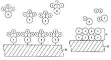
- FIG. 3is a schematic view showing deposition of a first molecule onto a substrate during ALD
- FIG. 4is a schematic view showing deposition of second molecule onto a substrate during ALD to form a refractory metal layer
- FIG. 5is a graphical representation showing the concentration of gases introduced into the processing chamber shown above in FIG. 2 , and the time in which the gases are present in the processing chamber, in accordance with the present invention
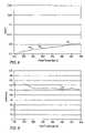
- FIG. 6is a graphical representation showing the relationship between the number of ALD cycles and the thickness of a layer formed on a substrate employing ALD, in accordance with the present invention
- FIG. 7is a graphical representation showing the relationship between the number of ALD cycles and the resistivity of a layer formed on a substrate employing ALD, in accordance with the present invention.
- FIG. 8is a graphical representation showing the relationship between the deposition rate of a layer formed on a substrate employing ALD and the temperature of the substrate;
- FIG. 9is a graphical representation showing the relationship between the resistivity of a layer formed on a substrate employing ALD and the temperature of the substrate, in accordance with the present invention.
- FIG. 10is a cross-sectional view of a patterned substrate having a nucleation layer formed thereon employing ALD, in accordance with the present invention.
- FIG. 11is a partial cross-sectional view of the substrate, shown above in FIG. 10 , with a refractory metal layer formed atop of the nucleation layer employing CVD, in accordance with the present invention
- FIG. 12is a graphical representation showing the concentration of gases shown above in FIG. 5 in accordance with a first alternate embodiment of the present invention.
- FIG. 13is a graphical representation showing the concentration of gases shown above in FIG. 5 in accordance with a second alternate embodiment of the present invention.
- FIG. 14is a graphical representation showing the fluorine content versus depth of a refractory metal layer formed on a substrate employing ALD either Ar or N 2 being a carrier gas;
- FIG. 15is a graphical representation showing the fluorine content versus depth of a refractory metal layer formed on a substrate employing ALD with H 2 being a carrier gas.
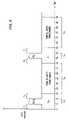
- an exemplary wafer processing systemincludes two or more processing chambers 12 and 14 disposed in a common work area 16 surrounded by a wall 18 .
- the processing chambers 12 and 14are in data communication with a controller 22 that is connected to one or more monitors, shown as 24 and 26 .
- the monitorstypically display common information concerning the process associated with the processing chambers 12 and 14 .
- One of the monitors 26is mounted to the wall 18 , with the remaining monitor 24 being disposed in the work area 16 .
- Operational control of the processing chambers 12 and 14may be achieved use of a light pen, associated with one of the monitors 24 and 26 , to communicate with the controller 22 .
- light pen 28is associated with monitor 24 and facilitates communication with the controller 22 through monitor 24 .
- Light pen 29facilitates communication with the controller 22 through monitor 26 .
- each of the processing chambers 12 and 14includes a housing 30 having a base wall 32 , a cover 34 , disposed opposite to the base wall 32 , and a sidewall 36 , extending therebetween.
- the housing 30defines a chamber 37 , and a pedestal 38 is disposed within the processing chamber 37 to support a substrate 42 , such as a semiconductor wafer.
- the pedestal 38may be mounted to move between the cover 34 and the base wall 32 , using a displacement mechanism (not shown).
- Supplies of processing gases 39 a , 39 b , and 39 care in fluid communication with the processing chamber 37 via a showerhead 40 . Regulation of the flow of gases from the supplies 39 a , 39 b and 39 c is effectuated via flow valves 41 .
- the substrate 42may be heated to a desired temperature prior to layer deposition via a heater embedded within the pedestal 38 .
- the pedestal 38may be resistively heated by applying an electric current from an AC power supply 43 to the heater element 44 .
- the wafer 40is, in turn, heated by the pedestal 38 , and can be maintained within a desired process temperature range of, for example, about 20° C. to about 750° C.
- a temperature sensor 46such as a thermocouple, is also embedded in the wafer support pedestal 38 to monitor the temperature of the pedestal 38 in a conventional manner.
- the measured temperaturemay be used in a feedback loop to control the electrical current applied to the heater element 44 by the power supply 43 , such that the wafer temperature can be maintained or controlled at a desired temperature which is suitable for the particular process application.
- the pedestal 38is optionally heated using radiant heat (not shown).
- a vacuum pump 48is used to evacuate the processing chamber 37 and to help maintain the proper gas flows and pressure inside the processing chamber 37 .
- one or both of the processing chambers 12 and 14may operate to deposit refractory metal layers on the substrate employing ALD techniques.
- the refractory metal layermay be deposited on the material from which the substrate 42 is fabricated, e.g., SiO 2 .
- the refractory metal layermay also be deposited on a layer previously formed on the substrate 42 , e.g., titanium, titanium nitride and the like.
- ALDproceeds by chemisorption.
- the initial surface of the substrate 42presents an active ligand to the process region.
- a batch of a first processing gasin this case Aa x , results in a layer of “A” being deposited on the substrate 42 having a surface of ligand “a” exposed to the processing chamber 37 .
- a purge gasenters the processing chamber 37 to purge the gas Aa x .
- a second batch of processing gas, Bb yis introduced into the processing chamber 37 .
- the a ligand present on the substrate surfacereacts with the “b” ligand and “B” atom on the, releasing molecules ab and Ba, that move away from the substrate 42 and are subsequently pumped from the processing chamber 37 .
- a surface comprising a monolayer of A atomsremains upon the substrate 42 and exposed to the processing chamber 37 , shown in FIG. 4 .
- the processproceeds cycle after cycle, until the desired thickness is achieved.
- the processing gas Aa xis WF 6 and the processing gas Bb y is B 2 H 6 .
- Two purge gaseswere employed: Ar and N 2 .
- Each of the processing gasesis flowed into the processing chamber 37 with a carrier gas, which in this example were one of the purge gases: WF 6 is introduced with Ar and B 2 H 6 is introduced with N 2 .
- WF 6is introduced with Ar
- B 2 H 6is introduced with N 2 .
- the purge gasmay differ from the carrier gas, discussed more fully below.
- One cycle of the ALD technique in accordance with the present inventionincludes flowing the purge gas, N 2 , into the processing chamber 37 during time t 1 , which is approximately five seconds before B 2 H 6 is flowed into the processing chamber 37 .
- the processing gas B 2 H 6is flowed into the processing chamber 37 for approximately five seconds, along with a carrier gas, which in this example is N 2 .
- a carrier gaswhich in this example is N 2 .
- the flow of B 2 H 6terminates and the flow of N 2 continues during time t 3 for an additional five seconds, purging the processing chamber of B 2 H 6 .
- time t 4the processing chamber 37 is pumped so as to remove all gases. The pumping process lasts approximately thirty seconds.
- the carrier gas Aris introduced for approximately five seconds during time t 5 , after which time the process gas WF 6 is introduced into the processing chamber 37 for about five seconds, along with the carrier gas Ar during time t 6 .
- the flow of the processing gas WF 6 into the processing chamber 37is terminated approximately five seconds after it commenced.
- the flow of Arcontinues for five additional seconds, during time t 7 .
- the processing chamber 37is pumped so as to remove all gases therein, during time t 8 .
- the pumping processlasts approximately thirty seconds, thereby concluding one cycle of the ALD technique in accordance with the present invention.
- the benefits of employing ALDare manifold, including flux-independence of layer formation that provides uniformity of deposition independent of the size of a substrate. For example, the measured difference of the layer uniformity and thickness measured between of 200 mm substrate and a 32 mm substrate deposited in the same chamber is negligible. This is due to the self-limiting characteristics of chemisorption. Further, the chemisorption characteristics contribute to near-perfect step coverage over complex topography.
- the thickness of the layer Amay be easily controlled while minimizing the resistance of the same by employing ALD.
- ALDthe slope of line 50 that the thickness of the tungsten layer A is proportional to the number of cycles employed to form the same.
- the resistivity of the tungsten layeris relatively independent of the thickness of the layer, as shown by the slope of line 52 in FIG. 7 .
- the thickness of a refractory metal layermay be easily controlled as a function of the cycling of the process gases introduced into the processing chamber with a negligible effect on the resistivity.
- control of the deposition ratewas found to be dependent upon the temperature of the substrate 42 .
- increasing the temperature of the substrate 42increased the deposition rate of the tungsten layer A.
- the deposition rateis shown to be approximately 2 ⁇ /cycle at 250° C.
- the deposition rateis approximately 5 ⁇ /cycle at a temperature of 450° C.
- the resistivity of the tungsten layeris virtually independent of the layer thickness, as shown by the slope of curve 59 , shown in FIG. 9 .
- the deposition rate of the tungsten layermay be controlled as a function of temperature without comprising the resistivity of the same. However, it is preferred to perform many processing steps at temperatures well below 450° C.
- a bifurcated deposition processmay be practiced in which nucleation of the refractory metal layer occurs in a different chamber than the formation of the remaining portion of the refractory metal layer.
- nucleation of a tungsten layeroccurs in chamber 12 employing the ALD techniques discussed above, with the substrate 42 being heated in the range of 200° C. to 400° C., and the processing chamber 37 being pressurized in the range of 1 to 10 Torr.
- a nucleation layer 60 of approximately 12 to 20 nmis formed on a patterned substrate 42 , shown in FIG. 10 .
- the substrate 42includes a barrier layer 61 and a patterned layer having a plurality of vias 63 .
- the nucleation layeris formed adjacent to the patterned layer covering the vias 63 .
- forming the nucleation layer 60 employing ALD techniquesprovides 100% step coverage.
- a bulk deposition of tungsten onto the nucleation layer 60occurs using CVD techniques, while the substrate 42 is disposed in processing chamber 14 , shown in FIG. 1 .
- the bulk depositionmay be performed using recipes well known in the art. In this manner, a tungsten layer 65 providing a complete plug fill is achieved on the patterned layer with vias having aspect ratios of approximately 6:1, shown in FIG. 11 .
- the carrier gasmay differ from the purge gas, as shown in FIG. 12 .
- the purge gaswhich is introduced at time intervals t 1 , t 3 , t 5 and t 7 comprises of Ar.
- the carrier gaswhich is introduced at time intervals t 2 and t 6 , comprises of N 2 .
- the gases introduced into the processing chamberinclude a mixture of B 2 H 6 and N 2 , and a time interval t 6 , the gas mixture includes WF 6 and N 2 .
- the pump process during time intervals t 4 and t 8is identical to the pump process discussed above with respect to FIG. 5 .
- FIG. 12shows a time intervals t 1 , t 3 , t 5 and t 7 .
- the carrier gaswhich is introduced at time intervals t 2 and t 6 , comprises of N 2 .
- the gases introduced into the processing chamberinclude a mixture of B 2 H 6 and N 2 , and a time interval t 6 , the gas mixture includes WF 6
- the carrier gas during time intervals t 2 and t 6comprises H 2 , with the purge gas introduced at time intervals t 1 , t 3 , t 5 and t 7 comprising of Ar.
- the pump processes at time intervals t 4 and t 8are as discussed above.
- the gas mixture introduced into the processing chamber 37consists of B 2 H 6 and H 2 , and WF 6 and H 2 , at time interval t 6 .
- An advantage realized by employing the H 2 carrier gasis that the stability of the tungsten layer A may be improved. Specifically, by comparing curve 66 in FIG. 14 with the curve 68 in FIG. 15 , it is seen that the concentration of fluorine in the nucleation layer 60 is much less when H 2 is employed as the carrier gas, as compared with use of N 2 or Ar as a carrier gas. Specifically, the apex and nadir of curve 66 show that the fluorine concentration reaches levels in excess of 1 ⁇ 10 21 atoms per cubic centimeter and only as low as just below 1 ⁇ 10 19 atoms per cubic centimeter.
- Curve 68shows that the fluorine concentration is well below 1 ⁇ 10 21 atoms per cubic centimeter at the apex and well below 1 ⁇ 10 17 atoms per cubic centimeter at the nadir.
- employing H 2 as the carrier gasprovides a much more stable film, i.e., the probability of fluorine diffusing into the substrate, or adjacent layer is reduced. This also reduces the resistance of the refractory metal layer by avoiding the formation of a metal fluoride that may result from the increased fluorine concentration.
- the stability of the nucleation layer, as well as the resistivity of the samemay be controlled as a function of the carrier gas employed. This is also true when a refractory metal layer is deposited entirely employing ALD techniques, i.e., without using other deposition techniques, such as CVD.
- the process for depositing the tungsten layermay be controlled using a computer program product that is executed by the controller 22 .
- the controller 22includes a central processing unit (CPU) 70 , a volatile memory, such as a random access memory (RAM) 72 and permanent storage media, such as a floppy disk drive for use with a floppy diskette, or hard disk drive 74 .
- the computer program codecan be written in any conventional computer readable programming language; for example, 68000 assembly language, C, C++, Pascal, FORTRAN, and the like. Suitable program code is entered into a single file, or multiple files, using a conventional text editor and stored or embodied in a computer-readable medium, such as the hard disk drive 74 .
- the codeis compiled and the resultant compiler code is then linked with an object code of precompiled WINDOWS® library routines.
- the system userinvokes the object code, causing the CPU 70 to load the code in RAM 72 .
- the CPU 70then reads and executes the code to perform the tasks identified in the program.
Landscapes
- Chemical & Material Sciences (AREA)
- Engineering & Computer Science (AREA)
- General Chemical & Material Sciences (AREA)
- Chemical Kinetics & Catalysis (AREA)
- Materials Engineering (AREA)
- Metallurgy (AREA)
- Organic Chemistry (AREA)
- Mechanical Engineering (AREA)
- Physics & Mathematics (AREA)
- Condensed Matter Physics & Semiconductors (AREA)
- General Physics & Mathematics (AREA)
- Manufacturing & Machinery (AREA)
- Computer Hardware Design (AREA)
- Microelectronics & Electronic Packaging (AREA)
- Power Engineering (AREA)
- Crystallography & Structural Chemistry (AREA)
- Inorganic Chemistry (AREA)
- Chemical Vapour Deposition (AREA)
- Electrodes Of Semiconductors (AREA)
Abstract
Description
This application is a continuation of U.S. Ser. No. 11/468,156, filed Aug. 29, 2006, and issued as U.S. Pat. No. 7,235,486, which is a continuation of U.S. Ser. No. 11/338,565, filed Jan. 24, 2006, and issued as U.S. Pat. No. 7,115,494, which is a continuation of U.S. Ser. No. 10/951,354, filed Sep. 29, 2004, and issued as U.S. Pat. No. 7,033,922, which is a continuation of U.S. Ser. No. 09/625,336, filed Jul. 25, 2000, and issued as U.S. Pat. No. 6,855,368, which is a divisional of U.S. Ser. No. 09/605,593, filed Jun. 28, 2000, and issued as U.S. Pat. No. 6,551,929, which are herein incorporated by reference in their entirety.
1. Field of the Invention
This invention relates to the processing of semiconductor substrates. More particularly, this invention relates to improvements in the process of depositing refractory metal layers on semiconductor substrates.
2. Description of the Related Art
The semiconductor processing industry continues to strive for larger production yields while increasing the uniformity of layers deposited on substrates having increasing larger surface areas. These same factors in combination with new materials also provide higher integration of circuits per unit area of the substrate. As circuit integration increases, the need for greater uniformity and process control regarding layer thickness rises. As a result, various technologies have been developed to deposit layers on substrates in a cost-effective manner, while maintaining control over the characteristics of the layer. Chemical vapor deposition (CVD) is one of the most common deposition processes employed for depositing layers on a substrate. CVD is a flux-dependent deposition technique that requires precise control of the substrate temperature and precursors introduced into the processing chamber in order to produce a desired layer of uniform thickness. These requirements become more critical as substrate size increases, creating a need for more complexity in chamber design and gas flow technique to maintain adequate uniformity.
A variant of CVD that demonstrates superior step coverage, compared to CVD, is atomic layer deposition (ALD). ALD is based upon atomic layer epitaxy (ALE) that was originally employed to fabricate electroluminescent displays. ALD employs chemisorption to deposit a saturated monolayer of reactive precursor molecules on a substrate surface. This is achieved by alternatingly pulsing an appropriate reactive precursor into a deposition chamber. Each injection of a reactive precursor is separated by an inert gas purge to provide a new atomic layer additive to previous deposited layers to form a uniform layer on the substrate. The cycle is repeated to form the layer to a desired thickness. A drawback with ALD techniques is that the deposition rate is much lower than typical CVD techniques by at least one order of magnitude.
Employing the aforementioned deposition techniques it is seen that formation of a layer at a high deposition rate while providing adequate step coverage are conflicting characteristics often necessitating sacrificing one to obtain the other. This has been prevalent when depositing refractory metal layers to cover gaps or vias during formation of contacts that interconnect adjacent metallic layers separated by a dielectric layer. Historically, CVD techniques have been employed to deposit conductive material in order to inexpensively and quickly form contacts. Due to the increasing integration of semiconductor circuitry, tungsten has been used based upon the superior step coverage of tungsten. As a result, deposition of tungsten employing CVD techniques enjoys wide application in semiconductor processing due to the high throughput of the process.
Depositing tungsten in this manner, however, is attendant with several disadvantages. For example, blanket deposition of a tungsten layer on a semiconductor wafer is time-consuming at temperatures below 400° C. The deposition rate of tungsten may be improved by increasing the deposition temperature to, e.g., about 500° C. to about 550° C. Temperatures in this range may compromise the structural and operational integrity of the underlying portions of the integrated circuit being formed. Tungsten has also frustrated photolithography steps during the manufacturing process by providing a relatively rough surface having a reflectivity of 20% or less than that of a silicon substrate. Finally, tungsten has proven difficult to deposit uniformly. This has been shown by variance in tungsten layers' thickness of greater than 1%, which frustrates control of the resistivity of the layer. Several prior attempts to overcome the aforementioned drawbacks have been attempted.
For example, in U.S. Pat. No. 5,028,565, which is assigned to the assignee of the present invention, a method is disclosed to improve, inter alia, uniformity of tungsten layers by varying the deposition chemistry. The method includes, in pertinent part, formation of a nucleation layer over an intermediate barrier layer before depositing the tungsten layer via bulk deposition. The nucleation layer is formed from a gaseous mixture of tungsten hexafluoride, hydrogen, silane and argon. The nucleation layer is described as providing a layer of growth sites to promote uniform deposition of a tungsten layer. The benefits provided by the nucleation layer are described as being dependent upon the barrier layer present. For example, were the barrier layer formed from titanium nitride, the tungsten layer's thickness uniformity is improved as much as 15%. The benefits provided by the nucleation layer are not substantial if the barrier layer is formed from sputtered tungsten or sputtered titanium tungsten.
A need exists, therefore, to provide techniques to improve the characteristics of refractory metal layers deposited on semiconductor substrates.
A method and system reduces the resistance of contacts of refractory metal layers by controlling the presence of fluorine contained therein. The present invention is based upon the discovery that when employing ALD techniques to form refractory metal layers on a substrate, the carrier gas employed impacts the presence of fluorine in the resulting layer. As a result, the method features chemisorbing onto the substrate alternating monolayers of a first compound and a second compound, with the second compound having fluorine atoms associated therewith, with each of the first and second compounds being introduced into the processing chamber along with a carrier gas; and controlling a quantity of the fluorine atoms associated with the monolayer of the second compound as a function of the carrier gas. Specifically, it was found that by introducing the first and second compounds employing H2as a carrier gas, the amount of fluorine present in the resulting refractory metal layer was substantially reduced, compared to employing either nitrogen (N2) or argon as a carrier gas.
To that end, the system includes a processing chamber, having a holder, disposed therein to support the substrate. A gas delivery system and a pressure control system are in fluid communication with the processing chamber. A temperature control system is in thermal communication therewith. A controller is in electrical communication with gas delivery system, temperature control system, and the pressure control system. A memory is in data communication with the controller. The memory comprises a computer-readable medium having a computer-readable program embodied therein. The computer-readable program includes instructions for controlling the operation of the processing chamber.
Referring toFIG. 1 , an exemplary wafer processing system includes two ormore processing chambers common work area 16 surrounded by awall 18. Theprocessing chambers controller 22 that is connected to one or more monitors, shown as24 and26. The monitors typically display common information concerning the process associated with theprocessing chambers monitors 26 is mounted to thewall 18, with the remainingmonitor 24 being disposed in thework area 16. Operational control of theprocessing chambers monitors controller 22. For example,light pen 28 is associated withmonitor 24 and facilitates communication with thecontroller 22 throughmonitor 24.Light pen 29 facilitates communication with thecontroller 22 throughmonitor 26.
Referring both toFIGS. 1 and 2 , each of theprocessing chambers housing 30 having abase wall 32, acover 34, disposed opposite to thebase wall 32, and asidewall 36, extending therebetween. Thehousing 30 defines achamber 37, and apedestal 38 is disposed within theprocessing chamber 37 to support asubstrate 42, such as a semiconductor wafer. Thepedestal 38 may be mounted to move between thecover 34 and thebase wall 32, using a displacement mechanism (not shown). Supplies of processinggases processing chamber 37 via ashowerhead 40. Regulation of the flow of gases from thesupplies flow valves 41.
Depending on the specific process, thesubstrate 42 may be heated to a desired temperature prior to layer deposition via a heater embedded within thepedestal 38. For example, thepedestal 38 may be resistively heated by applying an electric current from anAC power supply 43 to theheater element 44. Thewafer 40 is, in turn, heated by thepedestal 38, and can be maintained within a desired process temperature range of, for example, about 20° C. to about 750° C.A temperature sensor 46, such as a thermocouple, is also embedded in thewafer support pedestal 38 to monitor the temperature of thepedestal 38 in a conventional manner. For example, the measured temperature may used in a feedback loop to control the electrical current applied to theheater element 44 by thepower supply 43, such that the wafer temperature can be maintained or controlled at a desired temperature which is suitable for the particular process application. Thepedestal 38 is optionally heated using radiant heat (not shown). Avacuum pump 48 is used to evacuate theprocessing chamber 37 and to help maintain the proper gas flows and pressure inside theprocessing chamber 37.
Referring toFIGS. 1 and 3 , one or both of theprocessing chambers substrate 42 is fabricated, e.g., SiO2. The refractory metal layer may also be deposited on a layer previously formed on thesubstrate 42, e.g., titanium, titanium nitride and the like.
ALD proceeds by chemisorption. The initial surface of thesubstrate 42 presents an active ligand to the process region. A batch of a first processing gas, in this case Aax, results in a layer of “A” being deposited on thesubstrate 42 having a surface of ligand “a” exposed to theprocessing chamber 37. Thereafter, a purge gas enters theprocessing chamber 37 to purge the gas Aax. After purging gas Aaxfrom theprocessing chamber 37, a second batch of processing gas, Bby, is introduced into theprocessing chamber 37. The a ligand present on the substrate surface reacts with the “b” ligand and “B” atom on the, releasing molecules ab and Ba, that move away from thesubstrate 42 and are subsequently pumped from theprocessing chamber 37. In this manner, a surface comprising a monolayer of A atoms remains upon thesubstrate 42 and exposed to theprocessing chamber 37, shown inFIG. 4 . The process proceeds cycle after cycle, until the desired thickness is achieved.
Referring to bothFIGS. 2 and 5 , although any type of processing gas may be employed, in the present example, the processing gas Aaxis WF6and the processing gas Bbyis B2H6. Two purge gases were employed: Ar and N2. Each of the processing gases is flowed into theprocessing chamber 37 with a carrier gas, which in this example were one of the purge gases: WF6is introduced with Ar and B2H6is introduced with N2. It should be understood, however, that the purge gas may differ from the carrier gas, discussed more fully below. One cycle of the ALD technique in accordance with the present invention includes flowing the purge gas, N2, into theprocessing chamber 37 during time t1, which is approximately five seconds before B2H6is flowed into theprocessing chamber 37. During time t2, the processing gas B2H6is flowed into theprocessing chamber 37 for approximately five seconds, along with a carrier gas, which in this example is N2. After five seconds have lapsed, the flow of B2H6terminates and the flow of N2continues during time t3for an additional five seconds, purging the processing chamber of B2H6. During time t4, theprocessing chamber 37 is pumped so as to remove all gases. The pumping process lasts approximately thirty seconds. After pumping of theprocess chamber 37, the carrier gas Ar is introduced for approximately five seconds during time t5, after which time the process gas WF6is introduced into theprocessing chamber 37 for about five seconds, along with the carrier gas Ar during time t6. The flow of the processing gas WF6into theprocessing chamber 37 is terminated approximately five seconds after it commenced. After the flow of WF6into theprocessing chamber 37 terminates, the flow of Ar continues for five additional seconds, during time t7. Thereafter, theprocessing chamber 37 is pumped so as to remove all gases therein, during time t8. As before, the pumping process lasts approximately thirty seconds, thereby concluding one cycle of the ALD technique in accordance with the present invention.
The benefits of employing ALD are manifold, including flux-independence of layer formation that provides uniformity of deposition independent of the size of a substrate. For example, the measured difference of the layer uniformity and thickness measured between of 200 mm substrate and a 32 mm substrate deposited in the same chamber is negligible. This is due to the self-limiting characteristics of chemisorption. Further, the chemisorption characteristics contribute to near-perfect step coverage over complex topography.
In addition, the thickness of the layer A, shown inFIG. 4 , may be easily controlled while minimizing the resistance of the same by employing ALD. With reference toFIG. 6 it is seen the slope ofline 50 that the thickness of the tungsten layer A is proportional to the number of cycles employed to form the same. The resistivity of the tungsten layer, however, is relatively independent of the thickness of the layer, as shown by the slope ofline 52 inFIG. 7 . Thus, employing ALD, the thickness of a refractory metal layer may be easily controlled as a function of the cycling of the process gases introduced into the processing chamber with a negligible effect on the resistivity.
Referring toFIG. 8 , control of the deposition rate was found to be dependent upon the temperature of thesubstrate 42. As shown by the slope ofline 54, increasing the temperature of thesubstrate 42 increased the deposition rate of the tungsten layer A. For example, atpoint 56, the deposition rate is shown to be approximately 2 Å/cycle at 250° C. However atpoint 58 the deposition rate is approximately 5 Å/cycle at a temperature of 450° C. The resistivity of the tungsten layer, however, is virtually independent of the layer thickness, as shown by the slope ofcurve 59, shown inFIG. 9 . As a result, the deposition rate of the tungsten layer may be controlled as a function of temperature without comprising the resistivity of the same. However, it is preferred to perform many processing steps at temperatures well below 450° C.
To that end, a bifurcated deposition process may be practiced in which nucleation of the refractory metal layer occurs in a different chamber than the formation of the remaining portion of the refractory metal layer. Specifically, in the present example, nucleation of a tungsten layer occurs inchamber 12 employing the ALD techniques discussed above, with thesubstrate 42 being heated in the range of 200° C. to 400° C., and theprocessing chamber 37 being pressurized in the range of 1 to 10 Torr. Anucleation layer 60 of approximately 12 to 20 nm is formed on a patternedsubstrate 42, shown inFIG. 10 . As shown, thesubstrate 42 includes abarrier layer 61 and a patterned layer having a plurality ofvias 63. The nucleation layer is formed adjacent to the patterned layer covering thevias 63. As shown, forming thenucleation layer 60 employing ALD techniques provides 100% step coverage. To decrease the time required to form a complete layer of tungsten, a bulk deposition of tungsten onto thenucleation layer 60 occurs using CVD techniques, while thesubstrate 42 is disposed in processingchamber 14, shown inFIG. 1 . The bulk deposition may be performed using recipes well known in the art. In this manner, atungsten layer 65 providing a complete plug fill is achieved on the patterned layer with vias having aspect ratios of approximately 6:1, shown inFIG. 11 .
As mentioned above, in an alternate embodiment of the present invention, the carrier gas may differ from the purge gas, as shown inFIG. 12 . The purge gas, which is introduced at time intervals t1, t3, t5and t7comprises of Ar. The carrier gas, which is introduced at time intervals t2and t6, comprises of N2. Thus, at time interval t2the gases introduced into the processing chamber include a mixture of B2H6and N2, and a time interval t6, the gas mixture includes WF6and N2. The pump process during time intervals t4and t8is identical to the pump process discussed above with respect toFIG. 5 . In yet another embodiment, shown inFIG. 13 , the carrier gas during time intervals t2and t6comprises H2, with the purge gas introduced at time intervals t1, t3, t5and t7comprising of Ar. The pump processes at time intervals t4and t8are as discussed above. As a result, at time interval t2the gas mixture introduced into theprocessing chamber 37 consists of B2H6and H2, and WF6and H2, at time interval t6.
An advantage realized by employing the H2carrier gas is that the stability of the tungsten layer A may be improved. Specifically, by comparingcurve 66 inFIG. 14 with thecurve 68 inFIG. 15 , it is seen that the concentration of fluorine in thenucleation layer 60 is much less when H2is employed as the carrier gas, as compared with use of N2or Ar as a carrier gas. Specifically, the apex and nadir ofcurve 66 show that the fluorine concentration reaches levels in excess of 1×10²¹atoms per cubic centimeter and only as low as just below 1×10¹⁹atoms per cubic centimeter.Curve 68, however, shows that the fluorine concentration is well below 1×10²¹atoms per cubic centimeter at the apex and well below 1×10¹⁷atoms per cubic centimeter at the nadir. Thus, employing H2as the carrier gas provides a much more stable film, i.e., the probability of fluorine diffusing into the substrate, or adjacent layer is reduced. This also reduces the resistance of the refractory metal layer by avoiding the formation of a metal fluoride that may result from the increased fluorine concentration. Thus, the stability of the nucleation layer, as well as the resistivity of the same, may be controlled as a function of the carrier gas employed. This is also true when a refractory metal layer is deposited entirely employing ALD techniques, i.e., without using other deposition techniques, such as CVD.
Referring again toFIG. 2 , the process for depositing the tungsten layer may be controlled using a computer program product that is executed by thecontroller 22. To that end, thecontroller 22 includes a central processing unit (CPU)70, a volatile memory, such as a random access memory (RAM)72 and permanent storage media, such as a floppy disk drive for use with a floppy diskette, orhard disk drive 74. The computer program code can be written in any conventional computer readable programming language; for example, 68000 assembly language, C, C++, Pascal, FORTRAN, and the like. Suitable program code is entered into a single file, or multiple files, using a conventional text editor and stored or embodied in a computer-readable medium, such as thehard disk drive 74. If the entered code text is in a high level language, the code is compiled and the resultant compiler code is then linked with an object code of precompiled WINDOWS® library routines. To execute the linked and compiled object code the system user invokes the object code, causing theCPU 70 to load the code inRAM 72. TheCPU 70 then reads and executes the code to perform the tasks identified in the program.
Although the invention has been described in terms of specific embodiments, one skilled in the art will recognize that various changes to the reaction conditions, i.e., temperature, pressure, film thickness and the like can be substituted and are meant to be included herein. In addition, other refractory metals may be deposited, in addition to tungsten, and other deposition techniques may be employed in lieu of CVD. For example, physical vapor deposition (PVD) techniques, or a combination of both CVD and PVD techniques may be employed. Therefore, the scope of the invention should not be based upon the foregoing description. Rather, the scope of the invention should be determined based upon the claims recited herein, including the full scope of equivalents thereof.
Claims (33)
1. A method for forming a tungsten material on a substrate surface, comprising:
heating a substrate within a deposition chamber to a deposition temperature;
exposing the substrate sequentially to diborane and a tungsten precursor gas to form a tungsten nucleation layer on the substrate during an atomic layer deposition process; and
exposing the substrate to a deposition gas comprising hydrogen gas and the tungsten precursor gas to form a tungsten bulk layer over the tungsten nucleation layer during a chemical vapor deposition process.
2. The method ofclaim 1 , further comprising exposing the substrate to an initiation gas prior to the atomic layer deposition process.
3. The method ofclaim 2 , wherein the initiation gas comprises nitrogen or argon.
4. The method ofclaim 3 , wherein the substrate is exposed to the initiation gas for about 5 seconds.
5. The method ofclaim 1 , wherein the substrate is exposed to a reducing gas comprising the diborane and hydrogen gas during the atomic layer deposition process.
6. The method ofclaim 5 , wherein the tungsten precursor gas comprises tungsten hexafluoride.
7. The method ofclaim 1 , wherein the tungsten nucleation layer is formed having a thickness within a range from about 10 Å to about 100 Å.
8. The method ofclaim 1 , wherein the deposition chamber is a single station within a deposition system.
9. The method ofclaim 1 , wherein the deposition chamber is a first deposition station within a deposition system containing multiple stations surrounded by a wall.
10. The method ofclaim 9 , further comprising:
positioning the substrate into a second deposition station subsequent the atomic layer deposition process and prior to the chemical vapor deposition process; and
forming the tungsten bulk layer within the second deposition station.
11. The method ofclaim 9 , further comprising:
positioning the substrate comprising the tungsten nucleation layer into a second deposition station within the deposition system; and
forming the tungsten bulk layer over the tungsten nucleation layer by the chemical vapor deposition process within the second deposition station.
12. The method ofclaim 1 , wherein the deposition chamber during the atomic layer deposition process has a pressure within a range from about 1 Torr to about 10 Torr.
13. The method ofclaim 12 , wherein the deposition temperature is within a range from about 200° C. to about 400° C.
14. A method for forming a tungsten material on a substrate surface, comprising:
exposing a substrate within a deposition chamber sequentially to a reducing gas and a tungsten precursor gas to form a tungsten nucleation layer on the substrate during an atomic layer deposition process; and
exposing the substrate to a deposition gas comprising hydrogen gas and the tungsten precursor gas to form a tungsten bulk layer over the tungsten nucleation layer during a chemical vapor deposition process.
15. The method ofclaim 14 , further comprising exposing the substrate to an initiation gas prior to the atomic layer deposition process.
16. The method ofclaim 15 , wherein the initiation gas comprises nitrogen or argon.
17. The method ofclaim 16 , wherein the substrate is exposed to the initiation gas for about 5 seconds.
18. The method ofclaim 15 , wherein the reducing gas comprises a gas selected from the group consisting of diborane, hydrogen, silane, derivatives thereof, and combinations thereof.
19. The method ofclaim 14 , wherein the reducing gas comprises diborane and hydrogen.
20. The method ofclaim 19 , wherein the tungsten precursor gas comprises tungsten hexafluoride.
21. The method ofclaim 14 , wherein the reducing gas comprises silane and hydrogen.
22. The method ofclaim 21 , wherein the tungsten precursor gas comprises tungsten hexafluoride.
23. The method ofclaim 14 , wherein the tungsten nucleation layer is formed having a thickness within a range from about 10 Å to about 100 Å.
24. The method ofclaim 14 , wherein the deposition chamber is a single station within a deposition system.
25. The method ofclaim 14 , wherein the deposition chamber is a first deposition station within a deposition system containing multiple stations surrounded by a wall.
26. The method ofclaim 25 , further comprising:
positioning the substrate into a second deposition station subsequent the atomic layer deposition process and prior to the chemical vapor deposition process; and
forming the tungsten bulk layer within the second deposition station.
27. The method ofclaim 25 , further comprising:
positioning the substrate comprising the tungsten nucleation layer into a second deposition station within the deposition system; and
forming the tungsten bulk layer over the tungsten nucleation layer by the chemical vapor deposition process within the second deposition station.
28. The method ofclaim 14 , wherein the deposition chamber during the atomic layer deposition process has a pressure within a range from about 1 Torr to about 10 Torr.
29. The method ofclaim 28 , wherein the substrate is heated to a deposition temperature within a range from about 200° C. to about 400° C. during the atomic layer deposition process.
30. A method for forming a tungsten material on a substrate surface, comprising:
positioning a substrate at a first deposition station within a deposition system comprising at least two deposition stations;
flowing a reducing gas into the first deposition station, whereby the reducing gas is adsorbed onto the substrate to form an adsorbed reducing gas layer;
purging the first deposition station;
exposing the substrate sequentially to a tungsten precursor gas and diborane to form a tungsten nucleation layer thereon during an atomic layer deposition process;
positioning the substrate at a second deposition station within the deposition system; and
exposing the substrate to the tungsten precursor gas and hydrogen gas to deposit a tungsten bulk layer over the tungsten nucleation layer by a chemical vapor deposition process.
31. The method ofclaim 30 , further comprising exposing the substrate to an initiation gas prior to the atomic layer deposition process.
32. The method ofclaim 31 , wherein the initiation gas comprises nitrogen or argon.
33. The method ofclaim 32 , wherein the substrate is exposed to the initiation gas for about 5 seconds.
Priority Applications (3)
| Application Number | Priority Date | Filing Date | Title |
|---|---|---|---|
| US11/766,121US7465666B2 (en) | 2000-06-28 | 2007-06-21 | Method for forming tungsten materials during vapor deposition processes |
| US12/335,983US7674715B2 (en) | 2000-06-28 | 2008-12-16 | Method for forming tungsten materials during vapor deposition processes |
| US12/645,117US7846840B2 (en) | 2000-06-28 | 2009-12-22 | Method for forming tungsten materials during vapor deposition processes |
Applications Claiming Priority (6)
| Application Number | Priority Date | Filing Date | Title |
|---|---|---|---|
| US09/605,593US6551929B1 (en) | 2000-06-28 | 2000-06-28 | Bifurcated deposition process for depositing refractory metal layers employing atomic layer deposition and chemical vapor deposition techniques |
| US09/625,336US6855368B1 (en) | 2000-06-28 | 2000-07-25 | Method and system for controlling the presence of fluorine in refractory metal layers |
| US10/951,354US7033922B2 (en) | 2000-06-28 | 2004-09-29 | Method and system for controlling the presence of fluorine in refractory metal layers |
| US11/338,565US7115494B2 (en) | 2000-06-28 | 2006-01-24 | Method and system for controlling the presence of fluorine in refractory metal layers |
| US11/468,156US7235486B2 (en) | 2000-06-28 | 2006-08-29 | Method for forming tungsten materials during vapor deposition processes |
| US11/766,121US7465666B2 (en) | 2000-06-28 | 2007-06-21 | Method for forming tungsten materials during vapor deposition processes |
Related Parent Applications (1)
| Application Number | Title | Priority Date | Filing Date |
|---|---|---|---|
| US11/468,156ContinuationUS7235486B2 (en) | 2000-06-28 | 2006-08-29 | Method for forming tungsten materials during vapor deposition processes |
Related Child Applications (1)
| Application Number | Title | Priority Date | Filing Date |
|---|---|---|---|
| US12/335,983ContinuationUS7674715B2 (en) | 2000-06-28 | 2008-12-16 | Method for forming tungsten materials during vapor deposition processes |
Publications (2)
| Publication Number | Publication Date |
|---|---|
| US20070254481A1 US20070254481A1 (en) | 2007-11-01 |
| US7465666B2true US7465666B2 (en) | 2008-12-16 |
Family
ID=24424341
Family Applications (8)
| Application Number | Title | Priority Date | Filing Date |
|---|---|---|---|
| US09/605,593Expired - LifetimeUS6551929B1 (en) | 2000-06-28 | 2000-06-28 | Bifurcated deposition process for depositing refractory metal layers employing atomic layer deposition and chemical vapor deposition techniques |
| US09/625,336Expired - LifetimeUS6855368B1 (en) | 2000-06-28 | 2000-07-25 | Method and system for controlling the presence of fluorine in refractory metal layers |
| US10/951,354Expired - LifetimeUS7033922B2 (en) | 2000-06-28 | 2004-09-29 | Method and system for controlling the presence of fluorine in refractory metal layers |
| US11/338,565Expired - LifetimeUS7115494B2 (en) | 2000-06-28 | 2006-01-24 | Method and system for controlling the presence of fluorine in refractory metal layers |
| US11/468,156Expired - LifetimeUS7235486B2 (en) | 2000-06-28 | 2006-08-29 | Method for forming tungsten materials during vapor deposition processes |
| US11/766,121Expired - Fee RelatedUS7465666B2 (en) | 2000-06-28 | 2007-06-21 | Method for forming tungsten materials during vapor deposition processes |
| US12/335,983Expired - Fee RelatedUS7674715B2 (en) | 2000-06-28 | 2008-12-16 | Method for forming tungsten materials during vapor deposition processes |
| US12/645,117Expired - Fee RelatedUS7846840B2 (en) | 2000-06-28 | 2009-12-22 | Method for forming tungsten materials during vapor deposition processes |
Family Applications Before (5)
| Application Number | Title | Priority Date | Filing Date |
|---|---|---|---|
| US09/605,593Expired - LifetimeUS6551929B1 (en) | 2000-06-28 | 2000-06-28 | Bifurcated deposition process for depositing refractory metal layers employing atomic layer deposition and chemical vapor deposition techniques |
| US09/625,336Expired - LifetimeUS6855368B1 (en) | 2000-06-28 | 2000-07-25 | Method and system for controlling the presence of fluorine in refractory metal layers |
| US10/951,354Expired - LifetimeUS7033922B2 (en) | 2000-06-28 | 2004-09-29 | Method and system for controlling the presence of fluorine in refractory metal layers |
| US11/338,565Expired - LifetimeUS7115494B2 (en) | 2000-06-28 | 2006-01-24 | Method and system for controlling the presence of fluorine in refractory metal layers |
| US11/468,156Expired - LifetimeUS7235486B2 (en) | 2000-06-28 | 2006-08-29 | Method for forming tungsten materials during vapor deposition processes |
Family Applications After (2)
| Application Number | Title | Priority Date | Filing Date |
|---|---|---|---|
| US12/335,983Expired - Fee RelatedUS7674715B2 (en) | 2000-06-28 | 2008-12-16 | Method for forming tungsten materials during vapor deposition processes |
| US12/645,117Expired - Fee RelatedUS7846840B2 (en) | 2000-06-28 | 2009-12-22 | Method for forming tungsten materials during vapor deposition processes |
Country Status (1)
| Country | Link |
|---|---|
| US (8) | US6551929B1 (en) |
Cited By (33)
| Publication number | Priority date | Publication date | Assignee | Title |
|---|---|---|---|---|
| US20090081866A1 (en)* | 2000-06-28 | 2009-03-26 | Sang-Hyeob Lee | Vapor deposition of tungsten materials |
| US7595263B2 (en) | 2003-06-18 | 2009-09-29 | Applied Materials, Inc. | Atomic layer deposition of barrier materials |
| US7605083B2 (en) | 2001-07-16 | 2009-10-20 | Applied Materials, Inc. | Formation of composite tungsten films |
| US7611990B2 (en) | 2001-07-25 | 2009-11-03 | Applied Materials, Inc. | Deposition methods for barrier and tungsten materials |
| US7674715B2 (en) | 2000-06-28 | 2010-03-09 | Applied Materials, Inc. | Method for forming tungsten materials during vapor deposition processes |
| US7695563B2 (en) | 2001-07-13 | 2010-04-13 | Applied Materials, Inc. | Pulsed deposition process for tungsten nucleation |
| US7745329B2 (en) | 2002-02-26 | 2010-06-29 | Applied Materials, Inc. | Tungsten nitride atomic layer deposition processes |
| US7745333B2 (en) | 2000-06-28 | 2010-06-29 | Applied Materials, Inc. | Methods for depositing tungsten layers employing atomic layer deposition techniques |
| US20100267235A1 (en)* | 2009-04-16 | 2010-10-21 | Feng Chen | Methods for depositing ultra thin low resistivity tungsten film for small critical dimension contacts and interconnects |
| US7867914B2 (en) | 2002-04-16 | 2011-01-11 | Applied Materials, Inc. | System and method for forming an integrated barrier layer |
| KR101040726B1 (en)* | 2008-12-30 | 2011-06-10 | 주식회사 메카로닉스 | Electrode layer formation method |
| US7964505B2 (en) | 2005-01-19 | 2011-06-21 | Applied Materials, Inc. | Atomic layer deposition of tungsten materials |
| US8853080B2 (en) | 2012-09-09 | 2014-10-07 | Novellus Systems, Inc. | Method for depositing tungsten film with low roughness and low resistivity |
| US9076843B2 (en) | 2001-05-22 | 2015-07-07 | Novellus Systems, Inc. | Method for producing ultra-thin tungsten layers with improved step coverage |
| US9153486B2 (en) | 2013-04-12 | 2015-10-06 | Lam Research Corporation | CVD based metal/semiconductor OHMIC contact for high volume manufacturing applications |
| US9159571B2 (en) | 2009-04-16 | 2015-10-13 | Lam Research Corporation | Tungsten deposition process using germanium-containing reducing agent |
| US9240347B2 (en) | 2012-03-27 | 2016-01-19 | Novellus Systems, Inc. | Tungsten feature fill |
| US9589808B2 (en) | 2013-12-19 | 2017-03-07 | Lam Research Corporation | Method for depositing extremely low resistivity tungsten |
| US9613818B2 (en) | 2015-05-27 | 2017-04-04 | Lam Research Corporation | Deposition of low fluorine tungsten by sequential CVD process |
| US9754824B2 (en) | 2015-05-27 | 2017-09-05 | Lam Research Corporation | Tungsten films having low fluorine content |
| US9953984B2 (en) | 2015-02-11 | 2018-04-24 | Lam Research Corporation | Tungsten for wordline applications |
| US9978605B2 (en) | 2015-05-27 | 2018-05-22 | Lam Research Corporation | Method of forming low resistivity fluorine free tungsten film without nucleation |
| US9997405B2 (en) | 2014-09-30 | 2018-06-12 | Lam Research Corporation | Feature fill with nucleation inhibition |
| US10256142B2 (en) | 2009-08-04 | 2019-04-09 | Novellus Systems, Inc. | Tungsten feature fill with nucleation inhibition |
| US20200035507A1 (en)* | 2018-07-30 | 2020-01-30 | Wonik Ips Co., Ltd. | Method of depositing tungsten |
| US11348795B2 (en) | 2017-08-14 | 2022-05-31 | Lam Research Corporation | Metal fill process for three-dimensional vertical NAND wordline |
| US11549175B2 (en) | 2018-05-03 | 2023-01-10 | Lam Research Corporation | Method of depositing tungsten and other metals in 3D NAND structures |
| US11705337B2 (en) | 2017-05-25 | 2023-07-18 | Applied Materials, Inc. | Tungsten defluorination by high pressure treatment |
| US11972952B2 (en) | 2018-12-14 | 2024-04-30 | Lam Research Corporation | Atomic layer deposition on 3D NAND structures |
| US12002679B2 (en) | 2019-04-11 | 2024-06-04 | Lam Research Corporation | High step coverage tungsten deposition |
| US12077858B2 (en) | 2019-08-12 | 2024-09-03 | Lam Research Corporation | Tungsten deposition |
| US12237221B2 (en) | 2019-05-22 | 2025-02-25 | Lam Research Corporation | Nucleation-free tungsten deposition |
| US12444651B2 (en) | 2022-06-28 | 2025-10-14 | Novellus Systems, Inc. | Tungsten feature fill with nucleation inhibition |
Families Citing this family (178)
| Publication number | Priority date | Publication date | Assignee | Title |
|---|---|---|---|---|
| US6482262B1 (en) | 1959-10-10 | 2002-11-19 | Asm Microchemistry Oy | Deposition of transition metal carbides |
| US6974766B1 (en) | 1998-10-01 | 2005-12-13 | Applied Materials, Inc. | In situ deposition of a low κ dielectric layer, barrier layer, etch stop, and anti-reflective coating for damascene application |
| US7554829B2 (en) | 1999-07-30 | 2009-06-30 | Micron Technology, Inc. | Transmission lines for CMOS integrated circuits |
| US20040224504A1 (en) | 2000-06-23 | 2004-11-11 | Gadgil Prasad N. | Apparatus and method for plasma enhanced monolayer processing |
| US6620723B1 (en)* | 2000-06-27 | 2003-09-16 | Applied Materials, Inc. | Formation of boride barrier layers using chemisorption techniques |
| US6936538B2 (en)* | 2001-07-16 | 2005-08-30 | Applied Materials, Inc. | Method and apparatus for depositing tungsten after surface treatment to improve film characteristics |
| US7101795B1 (en) | 2000-06-28 | 2006-09-05 | Applied Materials, Inc. | Method and apparatus for depositing refractory metal layers employing sequential deposition techniques to form a nucleation layer |
| US20020036780A1 (en)* | 2000-09-27 | 2002-03-28 | Hiroaki Nakamura | Image processing apparatus |
| US20030190424A1 (en)* | 2000-10-20 | 2003-10-09 | Ofer Sneh | Process for tungsten silicide atomic layer deposition |
| US6827796B2 (en)* | 2000-11-02 | 2004-12-07 | Composite Tool Company, Inc. | High strength alloys and methods for making same |
| CN100446218C (en)* | 2000-11-17 | 2008-12-24 | 东京毅力科创株式会社 | Method for forming metal film and method for forming tungsten film |
| SG98018A1 (en)* | 2000-12-08 | 2003-08-20 | Inst Materials Research & Eng | A method of fabricating a semiconductor structure having quantum wires and a semiconductor device including such structure |
| US20020102797A1 (en)* | 2001-02-01 | 2002-08-01 | Muller David A. | Composite gate dielectric layer |
| US6951804B2 (en)* | 2001-02-02 | 2005-10-04 | Applied Materials, Inc. | Formation of a tantalum-nitride layer |
| US6852167B2 (en) | 2001-03-01 | 2005-02-08 | Micron Technology, Inc. | Methods, systems, and apparatus for uniform chemical-vapor depositions |
| US6596643B2 (en)* | 2001-05-07 | 2003-07-22 | Applied Materials, Inc. | CVD TiSiN barrier for copper integration |
| US7005372B2 (en)* | 2003-01-21 | 2006-02-28 | Novellus Systems, Inc. | Deposition of tungsten nitride |
| US7262125B2 (en)* | 2001-05-22 | 2007-08-28 | Novellus Systems, Inc. | Method of forming low-resistivity tungsten interconnects |
| US7589017B2 (en)* | 2001-05-22 | 2009-09-15 | Novellus Systems, Inc. | Methods for growing low-resistivity tungsten film |
| US7141494B2 (en)* | 2001-05-22 | 2006-11-28 | Novellus Systems, Inc. | Method for reducing tungsten film roughness and improving step coverage |
| US7955972B2 (en) | 2001-05-22 | 2011-06-07 | Novellus Systems, Inc. | Methods for growing low-resistivity tungsten for high aspect ratio and small features |
| US6849545B2 (en) | 2001-06-20 | 2005-02-01 | Applied Materials, Inc. | System and method to form a composite film stack utilizing sequential deposition techniques |
| US20070009658A1 (en)* | 2001-07-13 | 2007-01-11 | Yoo Jong H | Pulse nucleation enhanced nucleation technique for improved step coverage and better gap fill for WCVD process |
| US8110489B2 (en) | 2001-07-25 | 2012-02-07 | Applied Materials, Inc. | Process for forming cobalt-containing materials |
| US20090004850A1 (en) | 2001-07-25 | 2009-01-01 | Seshadri Ganguli | Process for forming cobalt and cobalt silicide materials in tungsten contact applications |
| US9051641B2 (en) | 2001-07-25 | 2015-06-09 | Applied Materials, Inc. | Cobalt deposition on barrier surfaces |
| JP2005504885A (en) | 2001-07-25 | 2005-02-17 | アプライド マテリアルズ インコーポレイテッド | Barrier formation using a novel sputter deposition method |
| KR100427030B1 (en)* | 2001-08-27 | 2004-04-14 | 주식회사 하이닉스반도체 | Method for forming film with muli-elements and fabricating capacitor using the same |
| JP4178776B2 (en)* | 2001-09-03 | 2008-11-12 | 東京エレクトロン株式会社 | Deposition method |
| US7049226B2 (en)* | 2001-09-26 | 2006-05-23 | Applied Materials, Inc. | Integration of ALD tantalum nitride for copper metallization |
| US6936906B2 (en) | 2001-09-26 | 2005-08-30 | Applied Materials, Inc. | Integration of barrier layer and seed layer |
| TW589684B (en)* | 2001-10-10 | 2004-06-01 | Applied Materials Inc | Method for depositing refractory metal layers employing sequential deposition techniques |
| US7780785B2 (en) | 2001-10-26 | 2010-08-24 | Applied Materials, Inc. | Gas delivery apparatus for atomic layer deposition |
| US6916398B2 (en)* | 2001-10-26 | 2005-07-12 | Applied Materials, Inc. | Gas delivery apparatus and method for atomic layer deposition |
| US7081271B2 (en)* | 2001-12-07 | 2006-07-25 | Applied Materials, Inc. | Cyclical deposition of refractory metal silicon nitride |
| US6900122B2 (en) | 2001-12-20 | 2005-05-31 | Micron Technology, Inc. | Low-temperature grown high-quality ultra-thin praseodymium gate dielectrics |
| US6911391B2 (en) | 2002-01-26 | 2005-06-28 | Applied Materials, Inc. | Integration of titanium and titanium nitride layers |
| US6998014B2 (en) | 2002-01-26 | 2006-02-14 | Applied Materials, Inc. | Apparatus and method for plasma assisted deposition |
| JP4074461B2 (en)* | 2002-02-06 | 2008-04-09 | 東京エレクトロン株式会社 | Film forming method, film forming apparatus, and semiconductor device manufacturing method |
| US6972267B2 (en) | 2002-03-04 | 2005-12-06 | Applied Materials, Inc. | Sequential deposition of tantalum nitride using a tantalum-containing precursor and a nitrogen-containing precursor |
| US6861094B2 (en)* | 2002-04-25 | 2005-03-01 | Micron Technology, Inc. | Methods for forming thin layers of materials on micro-device workpieces |
| US7160577B2 (en) | 2002-05-02 | 2007-01-09 | Micron Technology, Inc. | Methods for atomic-layer deposition of aluminum oxides in integrated circuits |
| US7589029B2 (en) | 2002-05-02 | 2009-09-15 | Micron Technology, Inc. | Atomic layer deposition and conversion |
| US6838114B2 (en)* | 2002-05-24 | 2005-01-04 | Micron Technology, Inc. | Methods for controlling gas pulsing in processes for depositing materials onto micro-device workpieces |
| US7041335B2 (en)* | 2002-06-04 | 2006-05-09 | Applied Materials, Inc. | Titanium tantalum nitride silicide layer |
| US7205218B2 (en)* | 2002-06-05 | 2007-04-17 | Micron Technology, Inc. | Method including forming gate dielectrics having multiple lanthanide oxide layers |
| US7135421B2 (en) | 2002-06-05 | 2006-11-14 | Micron Technology, Inc. | Atomic layer-deposited hafnium aluminum oxide |
| US7118783B2 (en)* | 2002-06-26 | 2006-10-10 | Micron Technology, Inc. | Methods and apparatus for vapor processing of micro-device workpieces |
| US7221586B2 (en) | 2002-07-08 | 2007-05-22 | Micron Technology, Inc. | Memory utilizing oxide nanolaminates |
| US6821347B2 (en)* | 2002-07-08 | 2004-11-23 | Micron Technology, Inc. | Apparatus and method for depositing materials onto microelectronic workpieces |
| US6838125B2 (en)* | 2002-07-10 | 2005-01-04 | Applied Materials, Inc. | Method of film deposition using activated precursor gases |
| US7186385B2 (en) | 2002-07-17 | 2007-03-06 | Applied Materials, Inc. | Apparatus for providing gas to a processing chamber |
| US6921702B2 (en)* | 2002-07-30 | 2005-07-26 | Micron Technology Inc. | Atomic layer deposited nanolaminates of HfO2/ZrO2 films as gate dielectrics |
| US6955725B2 (en) | 2002-08-15 | 2005-10-18 | Micron Technology, Inc. | Reactors with isolated gas connectors and methods for depositing materials onto micro-device workpieces |
| US7084078B2 (en)* | 2002-08-29 | 2006-08-01 | Micron Technology, Inc. | Atomic layer deposited lanthanide doped TiOx dielectric films |
| US6770536B2 (en)* | 2002-10-03 | 2004-08-03 | Agere Systems Inc. | Process for semiconductor device fabrication in which a insulating layer is formed on a semiconductor substrate |
| US20040074438A1 (en)* | 2002-10-22 | 2004-04-22 | Taiwan Semiconductor Manufacturing Company | Novel method to reduce resistivity of atomic layer tungsten chemical vapor depositon |
| EP1420080A3 (en) | 2002-11-14 | 2005-11-09 | Applied Materials, Inc. | Apparatus and method for hybrid chemical deposition processes |
| US7101813B2 (en) | 2002-12-04 | 2006-09-05 | Micron Technology Inc. | Atomic layer deposited Zr-Sn-Ti-O films |
| US6958302B2 (en) | 2002-12-04 | 2005-10-25 | Micron Technology, Inc. | Atomic layer deposited Zr-Sn-Ti-O films using TiI4 |
| KR100477816B1 (en)* | 2002-12-30 | 2005-03-22 | 주식회사 하이닉스반도체 | Method for forming titanium silicide contact of semiconductor device |
| US7244683B2 (en)* | 2003-01-07 | 2007-07-17 | Applied Materials, Inc. | Integration of ALD/CVD barriers with porous low k materials |
| US6926775B2 (en)* | 2003-02-11 | 2005-08-09 | Micron Technology, Inc. | Reactors with isolated gas connectors and methods for depositing materials onto micro-device workpieces |
| US7192892B2 (en)* | 2003-03-04 | 2007-03-20 | Micron Technology, Inc. | Atomic layer deposited dielectric layers |
| US7183186B2 (en)* | 2003-04-22 | 2007-02-27 | Micro Technology, Inc. | Atomic layer deposited ZrTiO4 films |
| US7335396B2 (en) | 2003-04-24 | 2008-02-26 | Micron Technology, Inc. | Methods for controlling mass flow rates and pressures in passageways coupled to reaction chambers and systems for depositing material onto microfeature workpieces in reaction chambers |
| US6844258B1 (en) | 2003-05-09 | 2005-01-18 | Novellus Systems, Inc. | Selective refractory metal and nitride capping |
| US7192824B2 (en) | 2003-06-24 | 2007-03-20 | Micron Technology, Inc. | Lanthanide oxide / hafnium oxide dielectric layers |
| US7344755B2 (en) | 2003-08-21 | 2008-03-18 | Micron Technology, Inc. | Methods and apparatus for processing microfeature workpieces; methods for conditioning ALD reaction chambers |
| US7235138B2 (en) | 2003-08-21 | 2007-06-26 | Micron Technology, Inc. | Microfeature workpiece processing apparatus and methods for batch deposition of materials on microfeature workpieces |
| US7754604B2 (en)* | 2003-08-26 | 2010-07-13 | Novellus Systems, Inc. | Reducing silicon attack and improving resistivity of tungsten nitride film |
| US7422635B2 (en) | 2003-08-28 | 2008-09-09 | Micron Technology, Inc. | Methods and apparatus for processing microfeature workpieces, e.g., for depositing materials on microfeature workpieces |
| US7056806B2 (en) | 2003-09-17 | 2006-06-06 | Micron Technology, Inc. | Microfeature workpiece processing apparatus and methods for controlling deposition of materials on microfeature workpieces |
| US7282239B2 (en)* | 2003-09-18 | 2007-10-16 | Micron Technology, Inc. | Systems and methods for depositing material onto microfeature workpieces in reaction chambers |
| US6924223B2 (en)* | 2003-09-30 | 2005-08-02 | Tokyo Electron Limited | Method of forming a metal layer using an intermittent precursor gas flow process |
| US20050069641A1 (en)* | 2003-09-30 | 2005-03-31 | Tokyo Electron Limited | Method for depositing metal layers using sequential flow deposition |
| US7323231B2 (en) | 2003-10-09 | 2008-01-29 | Micron Technology, Inc. | Apparatus and methods for plasma vapor deposition processes |
| US7581511B2 (en) | 2003-10-10 | 2009-09-01 | Micron Technology, Inc. | Apparatus and methods for manufacturing microfeatures on workpieces using plasma vapor processes |
| US7647886B2 (en)* | 2003-10-15 | 2010-01-19 | Micron Technology, Inc. | Systems for depositing material onto workpieces in reaction chambers and methods for removing byproducts from reaction chambers |
| US20050095859A1 (en)* | 2003-11-03 | 2005-05-05 | Applied Materials, Inc. | Precursor delivery system with rate control |
| US7258892B2 (en) | 2003-12-10 | 2007-08-21 | Micron Technology, Inc. | Methods and systems for controlling temperature during microfeature workpiece processing, e.g., CVD deposition |
| US7906393B2 (en) | 2004-01-28 | 2011-03-15 | Micron Technology, Inc. | Methods for forming small-scale capacitor structures |
| US7584942B2 (en) | 2004-03-31 | 2009-09-08 | Micron Technology, Inc. | Ampoules for producing a reaction gas and systems for depositing materials onto microfeature workpieces in reaction chambers |
| US8133554B2 (en) | 2004-05-06 | 2012-03-13 | Micron Technology, Inc. | Methods for depositing material onto microfeature workpieces in reaction chambers and systems for depositing materials onto microfeature workpieces |
| US20050252449A1 (en) | 2004-05-12 | 2005-11-17 | Nguyen Son T | Control of gas flow and delivery to suppress the formation of particles in an MOCVD/ALD system |
| US20060062917A1 (en)* | 2004-05-21 | 2006-03-23 | Shankar Muthukrishnan | Vapor deposition of hafnium silicate materials with tris(dimethylamino)silane |
| US8323754B2 (en) | 2004-05-21 | 2012-12-04 | Applied Materials, Inc. | Stabilization of high-k dielectric materials |
| US7699932B2 (en) | 2004-06-02 | 2010-04-20 | Micron Technology, Inc. | Reactors, systems and methods for depositing thin films onto microfeature workpieces |
| US20050287806A1 (en)* | 2004-06-24 | 2005-12-29 | Hiroyuki Matsuura | Vertical CVD apparatus and CVD method using the same |
| US7081421B2 (en) | 2004-08-26 | 2006-07-25 | Micron Technology, Inc. | Lanthanide oxide dielectric layer |
| US7494939B2 (en) | 2004-08-31 | 2009-02-24 | Micron Technology, Inc. | Methods for forming a lanthanum-metal oxide dielectric layer |
| US7588988B2 (en) | 2004-08-31 | 2009-09-15 | Micron Technology, Inc. | Method of forming apparatus having oxide films formed using atomic layer deposition |
| US7429402B2 (en)* | 2004-12-10 | 2008-09-30 | Applied Materials, Inc. | Ruthenium as an underlayer for tungsten film deposition |
| US20060125030A1 (en)* | 2004-12-13 | 2006-06-15 | Micron Technology, Inc. | Hybrid ALD-CVD of PrxOy/ZrO2 films as gate dielectrics |
| US7235501B2 (en)* | 2004-12-13 | 2007-06-26 | Micron Technology, Inc. | Lanthanum hafnium oxide dielectrics |
| US7560395B2 (en) | 2005-01-05 | 2009-07-14 | Micron Technology, Inc. | Atomic layer deposited hafnium tantalum oxide dielectrics |
| US7508648B2 (en)* | 2005-02-08 | 2009-03-24 | Micron Technology, Inc. | Atomic layer deposition of Dy doped HfO2 films as gate dielectrics |
| US7498247B2 (en)* | 2005-02-23 | 2009-03-03 | Micron Technology, Inc. | Atomic layer deposition of Hf3N4/HfO2 films as gate dielectrics |
| US7687409B2 (en) | 2005-03-29 | 2010-03-30 | Micron Technology, Inc. | Atomic layer deposited titanium silicon oxide films |
| US20060237138A1 (en)* | 2005-04-26 | 2006-10-26 | Micron Technology, Inc. | Apparatuses and methods for supporting microelectronic devices during plasma-based fabrication processes |
| US7662729B2 (en) | 2005-04-28 | 2010-02-16 | Micron Technology, Inc. | Atomic layer deposition of a ruthenium layer to a lanthanide oxide dielectric layer |
| US7390756B2 (en)* | 2005-04-28 | 2008-06-24 | Micron Technology, Inc. | Atomic layer deposited zirconium silicon oxide films |
| US7927948B2 (en) | 2005-07-20 | 2011-04-19 | Micron Technology, Inc. | Devices with nanocrystals and methods of formation |
| US8110469B2 (en) | 2005-08-30 | 2012-02-07 | Micron Technology, Inc. | Graded dielectric layers |
| TWI332532B (en)* | 2005-11-04 | 2010-11-01 | Applied Materials Inc | Apparatus and process for plasma-enhanced atomic layer deposition |
| US7658802B2 (en)* | 2005-11-22 | 2010-02-09 | Applied Materials, Inc. | Apparatus and a method for cleaning a dielectric film |
| US7537804B2 (en)* | 2006-04-28 | 2009-05-26 | Micron Technology, Inc. | ALD methods in which two or more different precursors are utilized with one or more reactants to form materials over substrates |
| US7798096B2 (en) | 2006-05-05 | 2010-09-21 | Applied Materials, Inc. | Plasma, UV and ion/neutral assisted ALD or CVD in a batch tool |
| EP2038072A1 (en)* | 2006-06-19 | 2009-03-25 | Universitetet I Oslo | Activation of surfaces through gas phase reactions |
| TWI395335B (en)* | 2006-06-30 | 2013-05-01 | Applied Materials Inc | Formation of nanocrystals |
| US7521379B2 (en)* | 2006-10-09 | 2009-04-21 | Applied Materials, Inc. | Deposition and densification process for titanium nitride barrier layers |
| JP5309436B2 (en)* | 2006-10-16 | 2013-10-09 | 日立化成株式会社 | Resin microstructure, method for producing the same, and polymerizable resin composition |
| US7775508B2 (en)* | 2006-10-31 | 2010-08-17 | Applied Materials, Inc. | Ampoule for liquid draw and vapor draw with a continuous level sensor |
| US7692222B2 (en)* | 2006-11-07 | 2010-04-06 | Raytheon Company | Atomic layer deposition in the formation of gate structures for III-V semiconductor |
| US8821637B2 (en)* | 2007-01-29 | 2014-09-02 | Applied Materials, Inc. | Temperature controlled lid assembly for tungsten nitride deposition |
| US7655567B1 (en) | 2007-07-24 | 2010-02-02 | Novellus Systems, Inc. | Methods for improving uniformity and resistivity of thin tungsten films |
| US20090032949A1 (en)* | 2007-08-02 | 2009-02-05 | Micron Technology, Inc. | Method of depositing Tungsten using plasma-treated tungsten nitride |
| WO2009064530A2 (en)* | 2007-08-30 | 2009-05-22 | Washington State University Research Foundation | Semiconductive materials and associated uses thereof |
| US20090087550A1 (en)* | 2007-09-27 | 2009-04-02 | Tokyo Electron Limited | Sequential flow deposition of a tungsten silicide gate electrode film |
| US7772114B2 (en)* | 2007-12-05 | 2010-08-10 | Novellus Systems, Inc. | Method for improving uniformity and adhesion of low resistivity tungsten film |
| US8053365B2 (en)* | 2007-12-21 | 2011-11-08 | Novellus Systems, Inc. | Methods for forming all tungsten contacts and lines |
| US8062977B1 (en) | 2008-01-31 | 2011-11-22 | Novellus Systems, Inc. | Ternary tungsten-containing resistive thin films |
| US7767572B2 (en)* | 2008-02-21 | 2010-08-03 | Applied Materials, Inc. | Methods of forming a barrier layer in an interconnect structure |
| US7618893B2 (en)* | 2008-03-04 | 2009-11-17 | Applied Materials, Inc. | Methods of forming a layer for barrier applications in an interconnect structure |
| US8058170B2 (en)* | 2008-06-12 | 2011-11-15 | Novellus Systems, Inc. | Method for depositing thin tungsten film with low resistivity and robust micro-adhesion characteristics |
| US8551885B2 (en)* | 2008-08-29 | 2013-10-08 | Novellus Systems, Inc. | Method for reducing tungsten roughness and improving reflectivity |
| US8491967B2 (en) | 2008-09-08 | 2013-07-23 | Applied Materials, Inc. | In-situ chamber treatment and deposition process |
| US20100062149A1 (en) | 2008-09-08 | 2010-03-11 | Applied Materials, Inc. | Method for tuning a deposition rate during an atomic layer deposition process |
| JP2010093116A (en)* | 2008-10-09 | 2010-04-22 | Panasonic Corp | Semiconductor device and method for manufacturing the same |
| US8146896B2 (en) | 2008-10-31 | 2012-04-03 | Applied Materials, Inc. | Chemical precursor ampoule for vapor deposition processes |
| US20100151676A1 (en)* | 2008-12-16 | 2010-06-17 | Applied Materials, Inc. | Densification process for titanium nitride layer for submicron applications |
| JP2010199349A (en)* | 2009-02-26 | 2010-09-09 | Toshiba Corp | Method for fabricating semiconductor device |
| US8207062B2 (en)* | 2009-09-09 | 2012-06-26 | Novellus Systems, Inc. | Method for improving adhesion of low resistivity tungsten/tungsten nitride layers |
| US8709948B2 (en) | 2010-03-12 | 2014-04-29 | Novellus Systems, Inc. | Tungsten barrier and seed for copper filled TSV |
| KR101205136B1 (en)* | 2010-12-17 | 2012-11-26 | 에스케이하이닉스 주식회사 | Semiconductor device and method for forming the same |
| CN103443906B (en) | 2011-03-04 | 2016-03-30 | 应用材料公司 | How to clean the contacts |
| US8912096B2 (en) | 2011-04-28 | 2014-12-16 | Applied Materials, Inc. | Methods for precleaning a substrate prior to metal silicide fabrication process |
| US9218961B2 (en) | 2011-09-19 | 2015-12-22 | Applied Materials, Inc. | Methods of forming a metal containing layer on a substrate with high uniformity and good profile control |
| US8927423B2 (en) | 2011-12-16 | 2015-01-06 | Applied Materials, Inc. | Methods for annealing a contact metal layer to form a metal silicidation layer |
| US8586479B2 (en) | 2012-01-23 | 2013-11-19 | Applied Materials, Inc. | Methods for forming a contact metal layer in semiconductor devices |
| US9330939B2 (en) | 2012-03-28 | 2016-05-03 | Applied Materials, Inc. | Method of enabling seamless cobalt gap-fill |
| US9034760B2 (en) | 2012-06-29 | 2015-05-19 | Novellus Systems, Inc. | Methods of forming tensile tungsten films and compressive tungsten films |
| US8975184B2 (en) | 2012-07-27 | 2015-03-10 | Novellus Systems, Inc. | Methods of improving tungsten contact resistance in small critical dimension features |
| US9169556B2 (en)* | 2012-10-11 | 2015-10-27 | Applied Materials, Inc. | Tungsten growth modulation by controlling surface composition |
| US9543163B2 (en) | 2013-08-20 | 2017-01-10 | Applied Materials, Inc. | Methods for forming features in a material layer utilizing a combination of a main etching and a cyclical etching process |
| TWI660429B (en) | 2013-09-27 | 2019-05-21 | 美商應用材料股份有限公司 | Method of enabling seamless cobalt gap-fill |
| JP5864503B2 (en)* | 2013-09-30 | 2016-02-17 | 株式会社日立国際電気 | Semiconductor device manufacturing method, substrate processing apparatus, program, and recording medium |
| US9508561B2 (en) | 2014-03-11 | 2016-11-29 | Applied Materials, Inc. | Methods for forming interconnection structures in an integrated cluster system for semicondcutor applications |
| US9528185B2 (en) | 2014-08-22 | 2016-12-27 | Applied Materials, Inc. | Plasma uniformity control by arrays of unit cell plasmas |
| US20170309490A1 (en)* | 2014-09-24 | 2017-10-26 | Hitachi Kokusai Electric Inc. | Method of manufacturing semiconductor device |
| KR102586409B1 (en)* | 2016-04-12 | 2023-10-11 | 피코순 오와이 | Coating by ALD to suppress metal whiskers |
| KR102727616B1 (en) | 2016-10-07 | 2024-11-07 | 삼성전자주식회사 | Organometallic precursors, methods of forming a layer using the same and methods of manufacturing semiconductor devices using the same |
| US10224224B2 (en) | 2017-03-10 | 2019-03-05 | Micromaterials, LLC | High pressure wafer processing systems and related methods |
| US10199267B2 (en) | 2017-06-30 | 2019-02-05 | Lam Research Corporation | Tungsten nitride barrier layer deposition |
| US10276411B2 (en) | 2017-08-18 | 2019-04-30 | Applied Materials, Inc. | High pressure and high temperature anneal chamber |
| WO2019036157A1 (en) | 2017-08-18 | 2019-02-21 | Applied Materials, Inc. | High pressure and high temperature anneal chamber |
| CN117936420A (en) | 2017-11-11 | 2024-04-26 | 微材料有限责任公司 | Gas delivery system for high pressure processing chamber |
| KR20200075892A (en) | 2017-11-17 | 2020-06-26 | 어플라이드 머티어리얼스, 인코포레이티드 | Condenser system for high pressure treatment systems |
| JP7018748B2 (en)* | 2017-11-28 | 2022-02-14 | 東京エレクトロン株式会社 | Film formation method and calculation method of film formation conditions |
| US11033930B2 (en) | 2018-01-08 | 2021-06-15 | Applied Materials, Inc. | Methods and apparatus for cryogenic gas stream assisted SAM-based selective deposition |
| SG11202008256WA (en) | 2018-03-09 | 2020-09-29 | Applied Materials Inc | High pressure annealing process for metal containing materials |
| US10633740B2 (en) | 2018-03-19 | 2020-04-28 | Applied Materials, Inc. | Methods for depositing coatings on aerospace components |
| US11015252B2 (en) | 2018-04-27 | 2021-05-25 | Applied Materials, Inc. | Protection of components from corrosion |
| US10950429B2 (en) | 2018-05-08 | 2021-03-16 | Applied Materials, Inc. | Methods of forming amorphous carbon hard mask layers and hard mask layers formed therefrom |
| US10748783B2 (en) | 2018-07-25 | 2020-08-18 | Applied Materials, Inc. | Gas delivery module |
| US11009339B2 (en) | 2018-08-23 | 2021-05-18 | Applied Materials, Inc. | Measurement of thickness of thermal barrier coatings using 3D imaging and surface subtraction methods for objects with complex geometries |
| US10636705B1 (en) | 2018-11-29 | 2020-04-28 | Applied Materials, Inc. | High pressure annealing of metal gate structures |
| WO2020117462A1 (en) | 2018-12-07 | 2020-06-11 | Applied Materials, Inc. | Semiconductor processing system |
| EP3959356A4 (en) | 2019-04-26 | 2023-01-18 | Applied Materials, Inc. | Methods of protecting aerospace components against corrosion and oxidation |
| US11794382B2 (en) | 2019-05-16 | 2023-10-24 | Applied Materials, Inc. | Methods for depositing anti-coking protective coatings on aerospace components |
| US11697879B2 (en) | 2019-06-14 | 2023-07-11 | Applied Materials, Inc. | Methods for depositing sacrificial coatings on aerospace components |
| US11466364B2 (en) | 2019-09-06 | 2022-10-11 | Applied Materials, Inc. | Methods for forming protective coatings containing crystallized aluminum oxide |
| US11901222B2 (en) | 2020-02-17 | 2024-02-13 | Applied Materials, Inc. | Multi-step process for flowable gap-fill film |
| US11519066B2 (en) | 2020-05-21 | 2022-12-06 | Applied Materials, Inc. | Nitride protective coatings on aerospace components and methods for making the same |
| WO2022005696A1 (en) | 2020-07-03 | 2022-01-06 | Applied Materials, Inc. | Methods for refurbishing aerospace components |
| JP7324740B2 (en)* | 2020-11-25 | 2023-08-10 | 株式会社Kokusai Electric | Substrate processing method, program, substrate processing apparatus, and semiconductor device manufacturing method |
| US11976002B2 (en) | 2021-01-05 | 2024-05-07 | Applied Materials, Inc. | Methods for encapsulating silver mirrors on optical structures |
| TW202429539A (en)* | 2023-01-13 | 2024-07-16 | 美商應用材料股份有限公司 | Low resistivity gapfill for logic devices |
Citations (545)
| Publication number | Priority date | Publication date | Assignee | Title |
|---|---|---|---|---|
| US4058430A (en) | 1974-11-29 | 1977-11-15 | Tuomo Suntola | Method for producing compound thin films |
| US4389973A (en) | 1980-03-18 | 1983-06-28 | Oy Lohja Ab | Apparatus for performing growth of compound thin films |
| JPS5898917U (en) | 1981-12-26 | 1983-07-05 | 株式会社フジ医療器 | Arm stretcher attached to chair-type pine surgery machine |
| JPS58100419U (en) | 1981-12-26 | 1983-07-08 | 株式会社 ブレスト工業研究所 | Conduit support for slab concrete pouring |
| US4413022A (en) | 1979-02-28 | 1983-11-01 | Canon Kabushiki Kaisha | Method for performing growth of compound thin films |
| US4486487A (en) | 1982-05-10 | 1984-12-04 | Oy Lohja Ab | Combination film, in particular for thin film electroluminescent structures |
| JPS6065712U (en) | 1983-10-05 | 1985-05-10 | 松下電工株式会社 | X-ray photograph observation device |
| JPS6169508U (en) | 1984-10-12 | 1986-05-13 | ||
| JPS61210623A (en) | 1985-03-15 | 1986-09-18 | Sony Corp | Manufacture of semiconductor device |
| JPS6135847Y2 (en) | 1980-11-05 | 1986-10-18 | ||
| JPS6291495U (en) | 1985-11-29 | 1987-06-11 | ||
| JPS62171999A (en) | 1986-01-27 | 1987-07-28 | Nippon Telegr & Teleph Corp <Ntt> | Epitaxy of iii-v compound semiconductor |
| JPS62141717U (en) | 1986-02-28 | 1987-09-07 | ||
| JPS62232919A (en) | 1986-04-02 | 1987-10-13 | Rikagaku Kenkyusho | Crystal growth |
| JPS62167297U (en) | 1986-04-14 | 1987-10-23 | ||
| JPS6385098U (en) | 1986-11-20 | 1988-06-03 | ||
| JPS6390833U (en) | 1986-12-03 | 1988-06-13 | ||
| US4767494A (en) | 1986-07-04 | 1988-08-30 | Nippon Telegraph & Telephone Corporation | Preparation process of compound semiconductor |
| JPS63222421A (en) | 1987-03-12 | 1988-09-16 | Nec Corp | Epitaxial growth method for atomic layer of iii-v compound semiconductor |
| JPS63222420A (en) | 1987-03-12 | 1988-09-16 | Nec Corp | Epitaxial growth method for atomic layer of iii-v compound semiconductor |
| JPS63227007A (en) | 1987-03-17 | 1988-09-21 | Matsushita Electric Ind Co Ltd | Vapor phase growth method |
| JPS63252420A (en) | 1987-04-09 | 1988-10-19 | Nec Corp | Compound semiconductor crystal and manufacture thereof |
| JPS63266814A (en) | 1987-04-24 | 1988-11-02 | Nec Corp | Forming method for al iii-v compound semiconductor thin film |
| JPS6362313B2 (en) | 1983-07-01 | 1988-12-01 | ||
| JPS649896B2 (en) | 1983-08-03 | 1989-02-20 | Hitachi Ltd | |
| JPS649895B2 (en) | 1982-02-22 | 1989-02-20 | Nitsushin Seiko Kk | |
| JPS649897B2 (en) | 1984-01-31 | 1989-02-20 | Topura Kk | |
| US4806321A (en) | 1984-07-26 | 1989-02-21 | Research Development Corporation Of Japan | Use of infrared radiation and an ellipsoidal reflection mirror |
| JPS6437832U (en) | 1987-09-02 | 1989-03-07 | ||
| US4813846A (en) | 1987-02-13 | 1989-03-21 | Leybold-Heraeus Gmbh | Inserting device for vacuum apparatus |
| JPS6482615A (en) | 1987-09-25 | 1989-03-28 | Nec Corp | Manufacture of semiconductor element |
| JPS6482671A (en) | 1987-09-25 | 1989-03-28 | Nec Corp | Manufacture of mis field-effect transistor |
| JPS6482617A (en) | 1987-09-25 | 1989-03-28 | Nec Corp | Method of epitaxial growth of atomic layer of regular mixed crystal |
| JPS6482676A (en) | 1987-09-25 | 1989-03-28 | Nec Corp | Iii-v compound semiconductor field-effect transistor and manufacture thereof |
| JPS6490524A (en) | 1987-10-01 | 1989-04-07 | Nec Corp | Manufacture of semiconductor device |
| JPH01103982A (en) | 1987-10-16 | 1989-04-21 | Nec Corp | Production of single crystal of group iii-v compound semiconductor |
| JPH01117017A (en) | 1987-10-29 | 1989-05-09 | Fujitsu Ltd | GaAs epitaxial growth method on Si substrate |
| US4829022A (en) | 1985-12-09 | 1989-05-09 | Nippon Telegraph And Telephone Corporation | Method for forming thin films of compound semiconductors by flow rate modulation epitaxy |
| US4834831A (en) | 1986-09-08 | 1989-05-30 | Research Development Corporation Of Japan | Method for growing single crystal thin films of element semiconductor |
| JPH01143221A (en) | 1987-11-27 | 1989-06-05 | Nec Corp | Manufacture of insulating thin film |
| JPH01143233A (en) | 1987-11-27 | 1989-06-05 | Nec Corp | Manufacture of semiconductor element |
| US4838993A (en) | 1986-12-04 | 1989-06-13 | Seiko Instruments Inc. | Method of fabricating MOS field effect transistor |
| US4838983A (en) | 1986-07-03 | 1989-06-13 | Emcore, Inc. | Gas treatment apparatus and method |
| JPH01154511A (en) | 1987-12-11 | 1989-06-16 | Hitachi Ltd | Crystal growth method |
| US4840921A (en) | 1987-07-01 | 1989-06-20 | Nec Corporation | Process for the growth of III-V group compound semiconductor crystal on a Si substrate |
| US4845049A (en) | 1987-03-27 | 1989-07-04 | Nec Corporation | Doping III-V compound semiconductor devices with group VI monolayers using ALE |
| JPH01103996U (en) | 1987-12-25 | 1989-07-13 | ||
| FR2626110A1 (en) | 1988-01-19 | 1989-07-21 | Thomson Csf | Process for producing a layer of a superconductive material by epitaxy |
| US4859625A (en) | 1986-11-22 | 1989-08-22 | Research Development Corporation of Japan, Junichi Nishizawa and Oki Electric Industry Co., Ltd. | Method for epitaxial growth of compound semiconductor using MOCVD with molecular layer epitaxy |
| US4859627A (en) | 1987-07-01 | 1989-08-22 | Nec Corporation | Group VI doping of III-V semiconductors during ALE |
| US4861417A (en) | 1987-03-27 | 1989-08-29 | Fujitsu Limited | Method of growing group III-V compound semiconductor epitaxial layer |
| JPH01236657A (en) | 1988-03-17 | 1989-09-21 | Toshiba Corp | Semiconductor device and manufacture thereof |
| JPH01245512A (en) | 1988-03-28 | 1989-09-29 | Nippon Telegr & Teleph Corp <Ntt> | Formation of iii-v compound semiconductor by epitaxial growth |
| JPH01264218A (en) | 1988-04-15 | 1989-10-20 | Fujitsu Ltd | Atomic layer epitaxial growth |
| US4876218A (en) | 1987-09-29 | 1989-10-24 | Oy Nokia Ab | Method of growing GaAs films on Si or GaAs substrates using ale |
| JPH01270593A (en) | 1988-04-21 | 1989-10-27 | Fujitsu Ltd | Compound semiconductor layer formation method |
| JPH01272108A (en) | 1988-04-25 | 1989-10-31 | Nippon Telegr & Teleph Corp <Ntt> | Growth of compound semiconductor |
| JPH01290221A (en) | 1988-05-18 | 1989-11-22 | Fujitsu Ltd | Semiconductor vapor phase growth method |
| JPH01290222A (en) | 1988-05-18 | 1989-11-22 | Fujitsu Ltd | Semiconductor vapor phase growth method |
| JPH01296673A (en) | 1988-05-25 | 1989-11-30 | Nec Corp | Iii-v compound semiconductor device |
| JPH01303770A (en) | 1988-06-01 | 1989-12-07 | Oki Electric Ind Co Ltd | Manufacture of superconductive base transistor |
| JPH01305894A (en) | 1988-06-03 | 1989-12-11 | Matsushita Electric Ind Co Ltd | Thin film crystal growth apparatus and growth method |
| JPH01313927A (en) | 1988-06-14 | 1989-12-19 | Fujitsu Ltd | Compound-semiconductor crystal growth method |
| WO1990002216A1 (en) | 1988-08-25 | 1990-03-08 | Vac-Tec Systems, Inc. | Physical vapor deposition dual coating apparatus and process |
| JPH0274587A (en) | 1988-09-09 | 1990-03-14 | Fujitsu Ltd | Thin film forming method and device |
| JPH0212814Y2 (en) | 1982-01-14 | 1990-04-10 | ||
| US4917556A (en) | 1986-04-28 | 1990-04-17 | Varian Associates, Inc. | Modular wafer transport and processing system |
| JPH02106822A (en) | 1988-10-14 | 1990-04-18 | Hitachi Ltd | Thin film forming method and thin film forming apparatus |
| JPH0214513Y2 (en) | 1983-10-29 | 1990-04-19 | ||
| JPH0217634Y2 (en) | 1985-05-28 | 1990-05-17 | ||
| US4927670A (en) | 1988-06-22 | 1990-05-22 | Georgia Tech Research Corporation | Chemical vapor deposition of mixed metal oxide coatings |
| US4931132A (en) | 1988-10-07 | 1990-06-05 | Bell Communications Research, Inc. | Optical control of deposition of crystal monolayers |
| JPH0274029U (en) | 1988-11-28 | 1990-06-06 | ||
| JPH02162717A (en) | 1988-12-15 | 1990-06-22 | Fujitsu Ltd | How to form quantum wires |
| JPH02172895A (en) | 1988-12-22 | 1990-07-04 | Nec Corp | Method for growing semiconductor crystal |
| JPH02196092A (en) | 1989-01-25 | 1990-08-02 | Sumitomo Electric Ind Ltd | Atomic layer epitaxial growth device of compound semiconductor |
| JPH02203517A (en) | 1989-02-01 | 1990-08-13 | Nec Corp | Selective vapor-phase epitaxy of iii-v compound semiconductor |
| US4951601A (en) | 1986-12-19 | 1990-08-28 | Applied Materials, Inc. | Multi-chamber integrated process system |
| JPH02230722A (en) | 1989-03-03 | 1990-09-13 | Nec Corp | Vapor growth method of compound semiconductor |
| JPH02230690A (en) | 1989-03-03 | 1990-09-13 | Fujitsu Ltd | Thin film el panel |
| JPH02246161A (en) | 1989-03-17 | 1990-10-01 | Fujitsu Ltd | Thin-film transistor |
| US4960720A (en) | 1986-08-26 | 1990-10-02 | Masafumi Shimbo | Method of growing compound semiconductor thin film using multichamber smoothing process |
| JPH02129913U (en) | 1989-03-31 | 1990-10-26 | ||
| JPH02264491A (en) | 1989-04-04 | 1990-10-29 | Mitsubishi Electric Corp | Manufacturing method of distributed feedback semiconductor laser |
| JPH02283084A (en) | 1989-04-25 | 1990-11-20 | Fujitsu Ltd | Manufacturing method of semiconductor laser |
| US4975252A (en) | 1984-07-26 | 1990-12-04 | Junichi Nishizawa | Semiconductor crystal growth apparatus |
| JPH02304916A (en) | 1989-05-19 | 1990-12-18 | Nec Corp | Vapor growing device for iii-v compound semiconductor |
| JPH0263115B2 (en) | 1983-06-29 | 1990-12-27 | Mtu Friedrichshafen Gmbh | |
| US4993357A (en) | 1987-12-23 | 1991-02-19 | Cs Halbleiter -Und Solartechnologie Gmbh | Apparatus for atomic layer epitaxial growth |
| JPH0319211B2 (en) | 1982-07-09 | 1991-03-14 | Shinnenryoyu Kaihatsu Gijutsu Kenkyu Kumiai | |
| US5000113A (en) | 1986-12-19 | 1991-03-19 | Applied Materials, Inc. | Thermal CVD/PECVD reactor and use for thermal chemical vapor deposition of silicon dioxide and in-situ multi-step planarized process |
| US5013683A (en) | 1989-01-23 | 1991-05-07 | The Regents Of The University Of California | Method for growing tilted superlattices |
| JPH0322569Y2 (en) | 1986-10-24 | 1991-05-16 | ||
| JPH0323299Y2 (en) | 1985-12-27 | 1991-05-21 | ||
| JPH0323294Y2 (en) | 1986-05-09 | 1991-05-21 | ||
| US5028565A (en) | 1989-08-25 | 1991-07-02 | Applied Materials, Inc. | Process for CVD deposition of tungsten layer on semiconductor wafer |
| JPH0348421B2 (en) | 1986-03-11 | 1991-07-24 | Yazaki Corp | |
| WO1991010510A1 (en) | 1990-01-16 | 1991-07-25 | Neste Oy | Process and apparatus for preparing heterogeneous catalysts |
| JPH03185716A (en) | 1989-12-14 | 1991-08-13 | Fujitsu Ltd | Method of growing compound semiconductor crystal |
| JPH03208885A (en) | 1990-01-09 | 1991-09-12 | Tdk Corp | Method for depositing oxide at atomic layer level by vapor growth method |
| JPH0344967Y2 (en) | 1990-10-17 | 1991-09-24 | ||
| JPH03234025A (en) | 1990-02-09 | 1991-10-18 | Fujitsu Ltd | Method of forming insulating thin film |
| JPH0370124B2 (en) | 1986-02-21 | 1991-11-06 | Ebara Mfg | |
| JPH03286522A (en) | 1990-04-03 | 1991-12-17 | Nec Corp | Growth method of si crystal |
| JPH03286531A (en) | 1990-04-02 | 1991-12-17 | Kawasaki Steel Corp | Formation of silicon oxide film |
| US5082798A (en) | 1990-04-18 | 1992-01-21 | Mitsubishi Denki Kabushiki Kaisha | Crystal growth method |
| US5085885A (en) | 1990-09-10 | 1992-02-04 | University Of Delaware | Plasma-induced, in-situ generation, transport and use or collection of reactive precursors |
| US5091320A (en) | 1990-06-15 | 1992-02-25 | Bell Communications Research, Inc. | Ellipsometric control of material growth |
| JPH04100292A (en) | 1990-08-20 | 1992-04-02 | Fujitsu Ltd | semiconductor laser |
| JPH04151822A (en) | 1990-10-15 | 1992-05-25 | Toshiba Corp | Metal-organic vapor phase growth method for compound semiconductors |
| JPH04162418A (en) | 1990-10-24 | 1992-06-05 | Fujitsu Ltd | Chemical vapor growth method |
| JPH04175299A (en) | 1990-11-09 | 1992-06-23 | Fujitsu Ltd | Compound semiconductor crystal growth and compound semiconductor device |
| JPH04186824A (en) | 1990-11-21 | 1992-07-03 | Fujitsu Ltd | Semiconductor substrate and its manufacturing method |
| US5130269A (en) | 1988-04-27 | 1992-07-14 | Fujitsu Limited | Hetero-epitaxially grown compound semiconductor substrate and a method of growing the same |
| JPH0431396Y2 (en) | 1987-05-14 | 1992-07-28 | ||
| JPH0431391Y2 (en) | 1986-07-15 | 1992-07-28 | ||
| JPH04212411A (en) | 1990-06-19 | 1992-08-04 | Nec Corp | Epitaxial growth method |
| JPH04260696A (en) | 1991-02-08 | 1992-09-16 | Fujitsu Ltd | Method for manufacturing compound semiconductor crystal |
| JPH04111418U (en) | 1991-03-19 | 1992-09-28 | 三菱重工業株式会社 | twin screw extruder |
| JPH04273120A (en) | 1991-02-27 | 1992-09-29 | Nec Corp | Region-selective crystal growth method |
| JPH04285167A (en) | 1991-03-15 | 1992-10-09 | Limes:Kk | Method for continuously forming thin film |
| JPH04291916A (en) | 1991-03-20 | 1992-10-16 | Kokusai Electric Co Ltd | Vapor phase growth method and apparatus |
| JPH04325500A (en) | 1991-04-26 | 1992-11-13 | Sanyo Electric Co Ltd | Method for controlling structure of crystalline surface |
| JPH04328874A (en) | 1991-04-27 | 1992-11-17 | Sanyo Electric Co Ltd | Electrostatic induction transistor and manufacture thereof |
| US5166092A (en) | 1988-01-28 | 1992-11-24 | Fujitsu Limited | Method of growing compound semiconductor epitaxial layer by atomic layer epitaxy |
| JPH04132214U (en) | 1991-02-01 | 1992-12-07 | ポツプリベツト・フアスナー株式会社 | Welding stud with cap |
| JPH04132681U (en) | 1991-05-30 | 1992-12-09 | 日本電気株式会社 | Magnetic disk assembly hand mechanism |
| US5173474A (en) | 1990-04-18 | 1992-12-22 | Xerox Corporation | Silicon substrate having an epitaxial superconducting layer thereon and method of making same |
| WO1993002111A1 (en) | 1991-07-16 | 1993-02-04 | Neste Oy | Process for preparing a polymerization catalyst by vapourizing chromium acetylacetonate |
| US5186718A (en) | 1989-05-19 | 1993-02-16 | Applied Materials, Inc. | Staged-vacuum wafer processing system and method |
| JPH05102189A (en) | 1991-08-13 | 1993-04-23 | Fujitsu Ltd | Thin film forming method, silicon thin film and silicon thin film transistor forming method |
| US5205077A (en) | 1990-08-31 | 1993-04-27 | Peter Wolters Ag | Apparatus for controlling operation of a lapping, honing or polishing machine |
| JPH05160152A (en) | 1991-12-05 | 1993-06-25 | Fujitsu Ltd | Manufacture of film transistor |
| US5225366A (en) | 1990-06-22 | 1993-07-06 | The United States Of America As Represented By The Secretary Of The Navy | Apparatus for and a method of growing thin films of elemental semiconductors |
| JPH05175143A (en) | 1991-12-26 | 1993-07-13 | Fujitsu Ltd | Manufacture of compound semiconductor device |
| JPH05175145A (en) | 1991-12-26 | 1993-07-13 | Fujitsu Ltd | Crystal growth method |
| JPH05182906A (en) | 1991-12-27 | 1993-07-23 | Sumitomo Electric Ind Ltd | Heteroepitaxial growth method |
| JPH0529228Y2 (en) | 1990-10-31 | 1993-07-27 | ||
| JPH05186295A (en) | 1992-01-13 | 1993-07-27 | Fujitsu Ltd | Crystal growth method |
| US5234561A (en) | 1988-08-25 | 1993-08-10 | Hauzer Industries Bv | Physical vapor deposition dual coating process |
| JPH05206036A (en) | 1992-01-30 | 1993-08-13 | Rikagaku Kenkyusho | Film formation method and film formation apparatus |
| JPH05234899A (en) | 1991-09-17 | 1993-09-10 | Hitachi Ltd | Atomic layer epitaxy system |
| JPH05235047A (en) | 1992-02-19 | 1993-09-10 | Nec Corp | Manufacture of field-effect transistor |
| US5246536A (en) | 1986-09-08 | 1993-09-21 | Research Development Corporation Of Japan | Method for growing single crystal thin films of element semiconductor |
| JPH05251339A (en) | 1991-08-14 | 1993-09-28 | Fujitsu Ltd | Semiconductor substrate and manufacturing method thereof |
| US5250148A (en) | 1985-05-15 | 1993-10-05 | Research Development Corporation | Process for growing GaAs monocrystal film |
| JPH05270997A (en) | 1992-03-19 | 1993-10-19 | Fujitsu Ltd | Atomic layer epitaxy apparatus and atomic layer epitaxy method |
| US5254207A (en) | 1991-11-30 | 1993-10-19 | Research Development Corporation Of Japan | Method of epitaxially growing semiconductor crystal using light as a detector |
| JPH0574724B2 (en) | 1987-04-27 | 1993-10-19 | Fischer Artur Werke Gmbh | |
| JPH0574717B2 (en) | 1986-02-14 | 1993-10-19 | Fuji Electric Co Ltd | |
| US5256244A (en) | 1992-02-10 | 1993-10-26 | General Electric Company | Production of diffuse reflective coatings by atomic layer epitaxy |
| JPH05283336A (en) | 1992-03-31 | 1993-10-29 | Nec Corp | Formation of compound semiconductor layer |
| JPH05291152A (en) | 1992-04-15 | 1993-11-05 | Hitachi Ltd | X-ray analyzer and semiconductor manufacturing apparatus using the same |
| US5259881A (en) | 1991-05-17 | 1993-11-09 | Materials Research Corporation | Wafer processing cluster tool batch preheating and degassing apparatus |
| JPH05304334A (en) | 1992-04-28 | 1993-11-16 | Nec Corp | Fabrication of semiconductor laser |
| US5270247A (en) | 1991-07-12 | 1993-12-14 | Fujitsu Limited | Atomic layer epitaxy of compound semiconductor |
| JPH0547668Y2 (en) | 1989-04-14 | 1993-12-15 | ||
| JPH0547666Y2 (en) | 1985-03-15 | 1993-12-15 | ||
| JPH0547665Y2 (en) | 1987-10-23 | 1993-12-15 | ||
| JPH05343685A (en) | 1992-06-05 | 1993-12-24 | Fujitsu Ltd | Manufacture of silicon thin film transistor |
| FR2692597A1 (en) | 1992-06-18 | 1993-12-24 | Mikrokemia Oy | Method and apparatus for introducing liquid phase reagents into a chemical reactor, and application of a coating to a substrate for chemical vapor deposition. |
| JPH05343327A (en) | 1992-06-12 | 1993-12-24 | Fujitsu Ltd | Film-forming method |
| US5278435A (en) | 1992-06-08 | 1994-01-11 | Apa Optics, Inc. | High responsivity ultraviolet gallium nitride detector |
| US5286296A (en) | 1991-01-10 | 1994-02-15 | Sony Corporation | Multi-chamber wafer process equipment having plural, physically communicating transfer means |
| US5290748A (en) | 1990-01-16 | 1994-03-01 | Neste Oy | Polymerization catalyst for olefines |
| US5294286A (en) | 1984-07-26 | 1994-03-15 | Research Development Corporation Of Japan | Process for forming a thin film of silicon |
| US5296403A (en) | 1990-01-31 | 1994-03-22 | Research Development Corp. Of Japan | Method of manufacturing a static induction field-effect transistor |
| US5306666A (en) | 1992-07-24 | 1994-04-26 | Nippon Steel Corporation | Process for forming a thin metal film by chemical vapor deposition |
| US5311055A (en) | 1991-11-22 | 1994-05-10 | The United States Of America As Represented By The Secretary Of The Navy | Trenched bipolar transistor structures |
| JPH06132236A (en) | 1992-10-20 | 1994-05-13 | Fujitsu Ltd | Method for manufacturing semiconductor device |
| US5316615A (en) | 1990-03-23 | 1994-05-31 | International Business Machines Corporation | Surfactant-enhanced epitaxy |
| US5316793A (en) | 1992-07-27 | 1994-05-31 | Texas Instruments Incorporated | Directed effusive beam atomic layer epitaxy system and method |
| JPH06177381A (en) | 1992-12-03 | 1994-06-24 | Fujitsu Ltd | Thin film transistor matrix and manufacturing method thereof |
| JPH06196809A (en) | 1992-12-22 | 1994-07-15 | Mitsubishi Electric Corp | Semiconductor optical device and manufacture thereof |
| US5330610A (en) | 1993-05-28 | 1994-07-19 | Martin Marietta Energy Systems, Inc. | Method of digital epilaxy by externally controlled closed-loop feedback |
| US5336324A (en) | 1991-12-04 | 1994-08-09 | Emcore Corporation | Apparatus for depositing a coating on a substrate |
| JPH06222388A (en) | 1993-01-28 | 1994-08-12 | Fujitsu Ltd | Production of thin film transistor matrix |
| US5338389A (en) | 1990-01-19 | 1994-08-16 | Research Development Corporation Of Japan | Method of epitaxially growing compound crystal and doping method therein |
| JPH06230421A (en) | 1993-02-02 | 1994-08-19 | Fujitsu Ltd | Method of manufacturing thin film transistor matrix |
| JPH06252057A (en) | 1993-02-24 | 1994-09-09 | Toshiba Corp | Manufacture of semiconductor device |
| US5348911A (en) | 1987-06-30 | 1994-09-20 | Aixtron Gmbh | Material-saving process for fabricating mixed crystals |
| EP0344352B1 (en) | 1988-06-03 | 1994-09-28 | International Business Machines Corporation | Method for making artificial layered high-Tc superconductors |
| JPH06291048A (en) | 1992-07-02 | 1994-10-18 | Nissin Electric Co Ltd | Thin-film formation method |
| JPH0645606Y2 (en) | 1988-03-07 | 1994-11-24 | マツダ株式会社 | Engine oil return device |
| US5395791A (en) | 1992-05-22 | 1995-03-07 | Minnesota Mining And Manufacturing Company | Growth of II VI laser diodes with quantum wells by atomic layer epitaxy and migration enhanced epitaxy |
| EP0442490B1 (en) | 1990-02-14 | 1995-05-03 | Sumitomo Electric Industries, Ltd. | Method for producing single crystal boron nitride film |
| JPH0770752B2 (en) | 1988-05-30 | 1995-07-31 | 日本電気株式会社 | Quantum interference device |
| US5438952A (en) | 1993-03-24 | 1995-08-08 | Fujitsu Limited | Method of growing a semiconductor layer and a fabrication method of a semiconductor device using such a semiconductor layer |
| US5441703A (en) | 1987-06-30 | 1995-08-15 | Aixtron Gmbh | Gas inlet for a plurality of reactant gases into reaction vessel |
| US5443647A (en) | 1993-04-28 | 1995-08-22 | The United States Of America As Represented By The Secretary Of The Army | Method and apparatus for depositing a refractory thin film by chemical vapor deposition |
| JPH0786269B2 (en) | 1990-11-30 | 1995-09-20 | 住友ゴム工業株式会社 | Tool for construction of sinking floor coating |
| US5455072A (en) | 1992-11-18 | 1995-10-03 | Bension; Rouvain M. | Initiation and bonding of diamond and other thin films |
| US5458084A (en) | 1992-04-16 | 1995-10-17 | Moxtek, Inc. | X-ray wave diffraction optics constructed by atomic layer epitaxy |
| JPH07300649A (en) | 1994-04-27 | 1995-11-14 | Kobe Steel Ltd | Hard film excellent in wear resistance and oxidation resistance and high hardness member |
| US5469806A (en) | 1992-08-21 | 1995-11-28 | Nec Corporation | Method for epitaxial growth of semiconductor crystal by using halogenide |
| US5480818A (en) | 1992-02-10 | 1996-01-02 | Fujitsu Limited | Method for forming a film and method for manufacturing a thin film transistor |
| US5483919A (en) | 1990-08-31 | 1996-01-16 | Nippon Telegraph And Telephone Corporation | Atomic layer epitaxy method and apparatus |
| US5503875A (en) | 1993-03-18 | 1996-04-02 | Tokyo Electron Limited | Film forming method wherein a partial pressure of a reaction byproduct in a processing container is reduced temporarily |
| US5521126A (en) | 1993-06-25 | 1996-05-28 | Nec Corporation | Method of fabricating semiconductor devices |
| WO1996017107A1 (en) | 1994-11-28 | 1996-06-06 | Mikrokemia Oy | Method and apparatus for growing thin films |
| US5526244A (en) | 1993-05-24 | 1996-06-11 | Bishop; Vernon R. | Overhead luminaire |
| US5527733A (en) | 1989-07-27 | 1996-06-18 | Seiko Instruments Inc. | Impurity doping method with adsorbed diffusion source |
| WO1996018756A1 (en) | 1994-12-16 | 1996-06-20 | Nkt Research Center A/S | A PA-CVD PROCESS FOR DEPOSITION OF A SOLID METAL-CONTAINING FILM ONTO A SUBSTRATE CONTAINING AT LEAST 50 % of Fe or WC |
| US5532511A (en) | 1992-10-23 | 1996-07-02 | Research Development Corp. Of Japan | Semiconductor device comprising a highspeed static induction transistor |
| JPH08181076A (en) | 1994-10-26 | 1996-07-12 | Fuji Xerox Co Ltd | Thin film forming method and device |
| EP0429270B1 (en) | 1989-11-20 | 1996-08-21 | Kokusai Electric Co., Ltd. | Continuous etching method and apparatus therefor |
| JPH08245291A (en) | 1995-03-10 | 1996-09-24 | Sumitomo Electric Ind Ltd | Method for growing III-V compound semiconductor crystal |
| JPH08264530A (en) | 1995-03-20 | 1996-10-11 | Fujitsu Ltd | Semiconductor device manufacturing method and semiconductor device manufacturing apparatus |
| US5580380A (en) | 1991-12-20 | 1996-12-03 | North Carolina State University | Method for forming a diamond coated field emitter and device produced thereby |
| DE19627017A1 (en) | 1995-07-07 | 1997-01-09 | Toshiba Kawasaki Kk | Process for the selective deposition of a metal film |
| US5601651A (en) | 1992-09-17 | 1997-02-11 | Fujitsu Limited | Flow control valve for use in fabrication of semiconductor devices |
| US5609689A (en) | 1995-06-09 | 1997-03-11 | Tokyo Electron Limited | Vacuum process apparaus |
| US5616181A (en) | 1994-11-24 | 1997-04-01 | Mitsubishi Denki Kabushiki Kaisha | MBE apparatus and gas branch piping apparatus |
| US5637530A (en) | 1991-09-09 | 1997-06-10 | U.S. Philips Corporation | II-VI compound semiconductor epitaxial layers having low defects, method for producing and devices utilizing same |
| US5641984A (en) | 1994-08-19 | 1997-06-24 | General Electric Company | Hermetically sealed radiation imager |
| US5644128A (en) | 1994-08-25 | 1997-07-01 | Ionwerks | Fast timing position sensitive detector |
| US5667592A (en) | 1996-04-16 | 1997-09-16 | Gasonics International | Process chamber sleeve with ring seals for isolating individual process modules in a common cluster |
| JPH09260786A (en) | 1996-03-22 | 1997-10-03 | Hitachi Ltd | Semiconductor light emitting device and method of manufacturing the same |
| US5674786A (en) | 1993-01-28 | 1997-10-07 | Applied Materials, Inc. | Method of heating and cooling large area glass substrates |
| EP0799641A2 (en) | 1996-04-03 | 1997-10-08 | Mikrokemia Oy | Functional surfaces for chemical reactions and process for the preparation thereof |
| JPH09293681A (en) | 1996-04-26 | 1997-11-11 | Sharp Corp | Vapor phase growth equipment |
| US5693139A (en) | 1984-07-26 | 1997-12-02 | Research Development Corporation Of Japan | Growth of doped semiconductor monolayers |
| US5695564A (en) | 1994-08-19 | 1997-12-09 | Tokyo Electron Limited | Semiconductor processing system |
| US5705224A (en) | 1991-03-20 | 1998-01-06 | Kokusai Electric Co., Ltd. | Vapor depositing method |
| US5711811A (en) | 1994-11-28 | 1998-01-27 | Mikrokemia Oy | Method and equipment for growing thin films |
| US5730802A (en) | 1994-05-20 | 1998-03-24 | Sharp Kabushiki Kaisha | Vapor growth apparatus and vapor growth method capable of growing good productivity |
| US5730801A (en) | 1994-08-23 | 1998-03-24 | Applied Materials, Inc. | Compartnetalized substrate processing chamber |
| US5747113A (en) | 1996-07-29 | 1998-05-05 | Tsai; Charles Su-Chang | Method of chemical vapor deposition for producing layer variation by planetary susceptor rotation |
| US5749974A (en) | 1994-07-15 | 1998-05-12 | Shin-Etsu Handotai Co., Ltd. | Method of chemical vapor deposition and reactor therefor |
| WO1998006889A3 (en) | 1996-08-16 | 1998-07-02 | Forward Technology Ind Inc | Superheated vapor dryer system |
| JPH10190128A (en) | 1996-12-27 | 1998-07-21 | Sony Corp | Manufacture of semiconductor light emitting device |
| JPH10188840A (en) | 1996-12-21 | 1998-07-21 | Korea Electron Telecommun | Light emitting particles for field emission display and method for forming light emitting layer for field emission display |
| US5788447A (en) | 1995-08-05 | 1998-08-04 | Kokusai Electric Co., Ltd. | Substrate processing apparatus |
| US5788799A (en) | 1996-06-11 | 1998-08-04 | Applied Materials, Inc. | Apparatus and method for cleaning of semiconductor process chamber surfaces |
| US5796116A (en) | 1994-07-27 | 1998-08-18 | Sharp Kabushiki Kaisha | Thin-film semiconductor device including a semiconductor film with high field-effect mobility |
| US5801634A (en) | 1997-09-08 | 1998-09-01 | Sony Corporation | Signal tower controller |
| US5804488A (en) | 1995-08-24 | 1998-09-08 | Taiwan Semiconductor Manufacturing Company, Ltd. | Method of forming a tungsten silicide capacitor having a high breakdown voltage |
| US5807792A (en) | 1996-12-18 | 1998-09-15 | Siemens Aktiengesellschaft | Uniform distribution of reactants in a device layer |
| US5830270A (en) | 1996-08-05 | 1998-11-03 | Lockheed Martin Energy Systems, Inc. | CaTiO3 Interfacial template structure on semiconductor-based material and the growth of electroceramic thin-films in the perovskite class |
| US5835677A (en) | 1996-10-03 | 1998-11-10 | Emcore Corporation | Liquid vaporizer system and method |
| US5834372A (en) | 1995-07-24 | 1998-11-10 | Lg Semicon., Ltd. | Pretreatment of semiconductor substrate |
| JPH10308283A (en) | 1997-03-04 | 1998-11-17 | Denso Corp | El element and its manufacture |
| WO1998051838A1 (en) | 1997-05-16 | 1998-11-19 | Applied Materials, Inc. | Low resistivity w using b2h¿6? |
| US5851849A (en) | 1997-05-22 | 1998-12-22 | Lucent Technologies Inc. | Process for passivating semiconductor laser structures with severe steps in surface topography |
| US5855680A (en) | 1994-11-28 | 1999-01-05 | Neste Oy | Apparatus for growing thin films |
| US5856219A (en) | 1992-12-02 | 1999-01-05 | Matsushita Electric Industrial Co., Ltd. | Method of fabricating a high-density dynamic random-access memory |
| US5855675A (en) | 1997-03-03 | 1999-01-05 | Genus, Inc. | Multipurpose processing chamber for chemical vapor deposition processes |
| WO1999001595A1 (en) | 1997-07-04 | 1999-01-14 | Asm Microchemistry Ltd | Method and apparatus for growing thin films |
| US5866213A (en) | 1994-06-03 | 1999-02-02 | Tokyo Electron Limited | Method for producing thin films by low temperature plasma-enhanced chemical vapor deposition using a rotating susceptor reactor |
| US5866795A (en) | 1997-03-17 | 1999-02-02 | Applied Materials, Inc. | Liquid flow rate estimation and verification by direct liquid measurement |
| US5879459A (en) | 1997-08-29 | 1999-03-09 | Genus, Inc. | Vertically-stacked process reactor and cluster tool system for atomic layer deposition |
| US5882165A (en) | 1986-12-19 | 1999-03-16 | Applied Materials, Inc. | Multiple chamber integrated process system |
| US5882413A (en) | 1997-07-11 | 1999-03-16 | Brooks Automation, Inc. | Substrate processing apparatus having a substrate transport with a front end extension and an internal substrate buffer |
| WO1999013504A1 (en) | 1997-09-10 | 1999-03-18 | Tokyo Electron Limited | A load-lock mechanism and processing apparatus |
| US5904565A (en) | 1997-07-17 | 1999-05-18 | Sharp Microelectronics Technology, Inc. | Low resistance contact between integrated circuit metal levels and method for same |
| WO1999029924A1 (en) | 1997-12-09 | 1999-06-17 | Asm Microchemistry Ltd. | Method for coating inner surfaces of equipment |
| US5916365A (en) | 1996-08-16 | 1999-06-29 | Sherman; Arthur | Sequential chemical vapor deposition |
| US5923056A (en) | 1996-10-10 | 1999-07-13 | Lucent Technologies Inc. | Electronic components with doped metal oxide dielectric materials and a process for making electronic components with doped metal oxide dielectric materials |
| US5923985A (en) | 1987-01-05 | 1999-07-13 | Seiko Instruments Inc. | MOS field effect transistor and its manufacturing method |
| US5925574A (en) | 1989-12-01 | 1999-07-20 | Seiko Instruments Inc. | Method of producing a bipolar transistor |
| US5928389A (en) | 1996-10-21 | 1999-07-27 | Applied Materials, Inc. | Method and apparatus for priority based scheduling of wafer processing within a multiple chamber semiconductor wafer processing tool |
| US5942040A (en) | 1996-08-27 | 1999-08-24 | Electronics And Telecommunications Research Institute | Multi-target manipulator for pulsed laser deposition apparatus |
| US5947710A (en) | 1995-12-07 | 1999-09-07 | Carrier Corporation | Rotary compressor with reduced lubrication sensitivity |
| JPH11269652A (en) | 1998-03-14 | 1999-10-05 | Samsung Electronics Co Ltd | Thin film manufacturing method |
| US5972430A (en) | 1997-11-26 | 1999-10-26 | Advanced Technology Materials, Inc. | Digital chemical vapor deposition (CVD) method for forming a multi-component oxide layer |
| WO1999041423A3 (en) | 1998-02-11 | 1999-10-28 | Applied Materials Inc | Plasma processes for depositing low dielectric constant films |
| US6001420A (en) | 1996-09-23 | 1999-12-14 | Applied Materials, Inc. | Semi-selective chemical vapor deposition |
| WO1999065064A1 (en) | 1998-06-05 | 1999-12-16 | A.S.M. International N.V. | Method and device for transferring wafers |
| US6015917A (en) | 1998-01-23 | 2000-01-18 | Advanced Technology Materials, Inc. | Tantalum amide precursors for deposition of tantalum nitride on a substrate |
| JP2000031387A (en) | 1998-07-14 | 2000-01-28 | Fuji Electric Co Ltd | Method of manufacturing dielectric thin film capacitor |
| US6025627A (en) | 1998-05-29 | 2000-02-15 | Micron Technology, Inc. | Alternate method and structure for improved floating gate tunneling devices |
| JP2000058777A (en) | 1998-08-12 | 2000-02-25 | Samsung Electronics Co Ltd | Capacitor having alumina / aluminum nitride composite dielectric film formed by atomic layer deposition method and method of manufacturing the same |
| WO2000011721A1 (en) | 1998-08-20 | 2000-03-02 | The Government Of The United States Of America, Represented By The Secretary Of The Navy | Electronic devices with barrier film and process for making same |
| JP2000068072A (en) | 1998-08-21 | 2000-03-03 | Planar Syst Inc | Thin-film electroluminescence device and method of manufacturing the same |
| US6036773A (en) | 1996-08-21 | 2000-03-14 | Agency Of Industrial Science & Technology, Ministry Of International Trade & Industry | Method for growing Group III atomic layer |
| WO2000015865A1 (en) | 1998-09-11 | 2000-03-23 | Asm Microchemistry Oy | Method for growing oxide thin films containing barium and strontium |
| US6043177A (en) | 1997-01-21 | 2000-03-28 | University Technology Corporation | Modification of zeolite or molecular sieve membranes using atomic layer controlled chemical vapor deposition |
| JP2000087029A (en) | 1998-06-03 | 2000-03-28 | Planar Syst Inc | Method for growing thin film electroluminescent structures |
| US6042652A (en) | 1999-05-01 | 2000-03-28 | P.K. Ltd | Atomic layer deposition apparatus for depositing atomic layer on multiple substrates |
| US6051286A (en) | 1997-02-12 | 2000-04-18 | Applied Materials, Inc. | High temperature, high deposition rate process and apparatus for depositing titanium layers |
| JP2000138094A (en) | 1998-08-14 | 2000-05-16 | Korea Electronics Telecommun | Method of manufacturing PBX (X = S, Se) thin film, electroluminescent device including PBX, and method of manufacturing the same |
| US6062798A (en) | 1996-06-13 | 2000-05-16 | Brooks Automation, Inc. | Multi-level substrate processing apparatus |
| US6071808A (en) | 1999-06-23 | 2000-06-06 | Lucent Technologies Inc. | Method of passivating copper interconnects in a semiconductor |
| WO2000015881A3 (en) | 1998-09-14 | 2000-06-08 | Genitech Co Ltd | Gas feeding system for chemical vapor deposition reactor and method of controlling the same |
| WO2000016377A3 (en) | 1998-09-10 | 2000-06-08 | Genitech Co Ltd | Method for forming a three-component nitride film containing metal and silicon |
| JP2000178735A (en) | 1998-12-18 | 2000-06-27 | Tokyo Electron Ltd | Method of forming tungsten film |
| US6084302A (en) | 1995-12-26 | 2000-07-04 | Micron Technologies, Inc. | Barrier layer cladding around copper interconnect lines |
| US6086677A (en) | 1998-06-16 | 2000-07-11 | Applied Materials, Inc. | Dual gas faceplate for a showerhead in a semiconductor wafer processing system |
| JP2000218445A (en) | 1999-02-03 | 2000-08-08 | Agency Of Ind Science & Technol | Surface improvement of machine element component |
| US6099904A (en) | 1997-12-02 | 2000-08-08 | Applied Materials, Inc. | Low resistivity W using B2 H6 nucleation step |
| US6110556A (en) | 1997-10-17 | 2000-08-29 | Applied Materials, Inc. | Lid assembly for a process chamber employing asymmetric flow geometries |
| US6113977A (en) | 1996-09-11 | 2000-09-05 | Planar International Oy Ltd. | Method of growing a ZnS:Mn phosphor layer for use in thin-film electroluminescent components |
| US6117244A (en) | 1998-03-24 | 2000-09-12 | Applied Materials, Inc. | Deposition resistant lining for CVD chamber |
| WO2000054320A1 (en) | 1999-03-11 | 2000-09-14 | Genus, Inc. | Radical-assisted sequential cvd |
| US6124158A (en) | 1999-06-08 | 2000-09-26 | Lucent Technologies Inc. | Method of reducing carbon contamination of a thin dielectric film by using gaseous organic precursors, inert gas, and ozone to react with carbon contaminants |
| US6130147A (en) | 1994-04-07 | 2000-10-10 | Sdl, Inc. | Methods for forming group III-V arsenide-nitride semiconductor materials |
| WO2000063957A1 (en) | 1999-04-06 | 2000-10-26 | Genitech, Inc. | Method of forming a thin film |
| US6140237A (en) | 1997-06-16 | 2000-10-31 | Chartered Semiconductor Manufacturing Ltd. | Damascene process for forming coplanar top surface of copper connector isolated by barrier layers in an insulating layer |
| US6139700A (en) | 1997-10-01 | 2000-10-31 | Samsung Electronics Co., Ltd. | Method of and apparatus for forming a metal interconnection in the contact hole of a semiconductor device |
| US6140238A (en) | 1997-09-03 | 2000-10-31 | National Semiconductor Corporation | Self-aligned copper interconnect structure and method of manufacturing same |
| US6144060A (en) | 1997-07-31 | 2000-11-07 | Samsung Electronics Co., Ltd. | Integrated circuit devices having buffer layers therein which contain metal oxide stabilized by heat treatment under low temperature |
| US6143659A (en) | 1997-11-18 | 2000-11-07 | Samsung Electronics, Co., Ltd. | Method for manufacturing aluminum metal interconnection layer by atomic layer deposition method |
| JP2000340883A (en) | 1999-05-27 | 2000-12-08 | Fujitsu Ltd | Multi-wavelength oscillation optical semiconductor device |
| US6158446A (en) | 1994-11-14 | 2000-12-12 | Fsi International | Ultra-low particle semiconductor cleaner |
| JP2000353666A (en) | 1999-06-11 | 2000-12-19 | Matsushita Electric Ind Co Ltd | Semiconductor thin film and method of manufacturing the same |
| US6162715A (en) | 1997-06-30 | 2000-12-19 | Applied Materials, Inc. | Method of forming gate electrode connection structure by in situ chemical vapor deposition of tungsten and tungsten nitride |
| WO2000079019A1 (en) | 1999-06-24 | 2000-12-28 | Prasad Narhar Gadgil | Apparatus for atomic layer chemical vapor deposition |
| WO2000079576A1 (en) | 1999-06-19 | 2000-12-28 | Genitech, Inc. | Chemical deposition reactor and method of forming a thin film using the same |
| US6174377B1 (en) | 1997-03-03 | 2001-01-16 | Genus, Inc. | Processing chamber for atomic layer deposition processes |
| US6174809B1 (en) | 1997-12-31 | 2001-01-16 | Samsung Electronics, Co., Ltd. | Method for forming metal layer using atomic layer deposition |
| JP2001020075A (en) | 1999-05-10 | 2001-01-23 | Asm Microchemistry Oy | Thin film manufacturing equipment |
| WO2001015220A1 (en) | 1999-08-24 | 2001-03-01 | Asm America, Inc. | Method for bottomless deposition of barrier layers in integrated circuit metallization schemes |
| US6197683B1 (en) | 1997-09-29 | 2001-03-06 | Samsung Electronics Co., Ltd. | Method of forming metal nitride film by chemical vapor deposition and method of forming metal contact of semiconductor device using the same |
| JP2001062244A (en) | 1999-07-20 | 2001-03-13 | Asm Microchemistry Oy | Method and device for removing material from gas |
| US6203613B1 (en) | 1999-10-19 | 2001-03-20 | International Business Machines Corporation | Atomic layer deposition with nitrate containing precursors |
| US6207487B1 (en) | 1998-10-13 | 2001-03-27 | Samsung Electronics Co., Ltd. | Method for forming dielectric film of capacitor having different thicknesses partly |
| US6218298B1 (en) | 1999-05-19 | 2001-04-17 | Infineon Technologies North America Corp. | Tungsten-filled deep trenches |
| WO2001027347A1 (en) | 1999-10-15 | 2001-04-19 | Asm Microchemistry Oy | Method of depositing transition metal nitride thin films |
| WO2001027346A1 (en) | 1999-10-15 | 2001-04-19 | Asm Microchemistry Oy | Method of modifying source chemicals in an ald process |
| JP2001111000A (en) | 1999-08-14 | 2001-04-20 | Samsung Electronics Co Ltd | Semiconductor device and manufacturing method thereof |
| WO2001029891A1 (en) | 1999-10-15 | 2001-04-26 | Asm America, Inc. | Conformal lining layers for damascene metallization |
| WO2001029893A1 (en) | 1999-10-15 | 2001-04-26 | Asm America, Inc. | Method for depositing nanolaminate thin films on sensitive surfaces |
| WO2001029280A1 (en) | 1999-10-15 | 2001-04-26 | Asm America, Inc. | Deposition of transition metal carbides |
| US20010000866A1 (en) | 1999-03-11 | 2001-05-10 | Ofer Sneh | Apparatus and concept for minimizing parasitic chemical vapor deposition during atomic layer deposition |
| WO2001036702A1 (en) | 1999-11-18 | 2001-05-25 | Genitech Co., Ltd. | Method of vaporizing liquid sources and apparatus therefor |
| JP2001152339A (en) | 1999-10-06 | 2001-06-05 | Samsung Electronics Co Ltd | Thin film formation method using atomic layer deposition |
| WO2001040541A1 (en) | 1999-12-03 | 2001-06-07 | Asm Microchemistry Oy | Atomic-layer-chemical-vapor-deposition of films that contain silicon dioxide |
| JP2001172767A (en) | 1999-10-14 | 2001-06-26 | Asm Microchemistry Oy | Oxide thin film growth method |
| JP2001189312A (en) | 1999-10-25 | 2001-07-10 | Motorola Inc | Method of manufacturing semiconductor structure having metal oxide interface with silicon |
| US20010009695A1 (en) | 2000-01-18 | 2001-07-26 | Saanila Ville Antero | Process for growing metalloid thin films |
| US6271148B1 (en) | 1997-04-23 | 2001-08-07 | Applied Materials, Inc. | Method for improved remote microwave plasma source for use with substrate processing system |
| US6270572B1 (en) | 1998-08-07 | 2001-08-07 | Samsung Electronics Co., Ltd. | Method for manufacturing thin film using atomic layer deposition |
| JP2001217206A (en) | 1999-12-08 | 2001-08-10 | Samsung Electronics Co Ltd | Metal layer forming method using atomic layer deposition and semiconductor device using the same |
| JP2001220294A (en) | 2000-02-04 | 2001-08-14 | Denso Corp | Method for forming film by atomic layer epitaxial growing method |
| US6274484B1 (en) | 2000-03-17 | 2001-08-14 | Taiwan Semiconductor Manufacturing Company | Fabrication process for low resistivity tungsten layer with good adhesion to insulator layers |
| JP2001220287A (en) | 2000-02-04 | 2001-08-14 | Denso Corp | Method and apparatus for thin film formation by atomic layer growth |
| JP2001240972A (en) | 2000-02-29 | 2001-09-04 | Denso Corp | Glass substrate storage jig for cvd and ale system |
| US6284646B1 (en) | 1997-08-19 | 2001-09-04 | Samsung Electronics Co., Ltd | Methods of forming smooth conductive layers for integrated circuit devices |
| US6287965B1 (en) | 1997-07-28 | 2001-09-11 | Samsung Electronics Co, Ltd. | Method of forming metal layer using atomic layer deposition and semiconductor device having the metal layer as barrier metal layer or upper or lower electrode of capacitor |
| JP2001254181A (en) | 2000-01-06 | 2001-09-18 | Tokyo Electron Ltd | Film depositing apparatus and film depositing method |
| US6291876B1 (en) | 1998-08-20 | 2001-09-18 | The United States Of America As Represented By The Secretary Of The Navy | Electronic devices with composite atomic barrier film and process for making same |
| US20010024387A1 (en) | 1999-12-03 | 2001-09-27 | Ivo Raaijmakers | Conformal thin films over textured capacitor electrodes |
| US20010025979A1 (en) | 1999-12-22 | 2001-10-04 | Min-Soo Kim | Semiconductor device incorporated therein high K capacitor dielectric and method for the manufacture thereof |
| US20010029094A1 (en) | 1998-09-17 | 2001-10-11 | Yoon Mee-Young | Semiconductor device fabrication method using an interface control layer to improve a metal interconnection layer |
| US20010028924A1 (en) | 1996-08-16 | 2001-10-11 | Arthur Sherman | Sequential chemical vapor deposition |
| JP2001284042A (en) | 2000-03-31 | 2001-10-12 | Denso Corp | Organic EL device |
| US20010031562A1 (en) | 2000-02-22 | 2001-10-18 | Ivo Raaijmakers | Method of forming ultrathin oxide layer |
| US6306216B1 (en) | 1999-07-15 | 2001-10-23 | Moohan Co., Ltd. | Apparatus for deposition of thin films on wafers through atomic layer epitaxial process |
| US6306098B1 (en) | 1996-12-19 | 2001-10-23 | Novametrix Medical Systems Inc. | Apparatus and method for non-invasively measuring cardiac output |
| US20010034123A1 (en) | 2000-04-20 | 2001-10-25 | In-Sang Jeon | Method of manufacturing a barrier metal layer using atomic layer deposition |
| US6309713B1 (en) | 1997-06-30 | 2001-10-30 | Applied Materials, Inc. | Deposition of tungsten nitride by plasma enhanced chemical vapor deposition |
| US20010041250A1 (en) | 2000-03-07 | 2001-11-15 | Werkhoven Christian J. | Graded thin films |
| US20010042799A1 (en) | 2000-02-16 | 2001-11-22 | Apex Co. Ltd. | Showerhead apparatus for radical-assisted deposition |
| JP2001328900A (en) | 2000-05-15 | 2001-11-27 | Denso Corp | Method for forming thin film |
| US6326297B1 (en) | 1999-09-30 | 2001-12-04 | Novellus Systems, Inc. | Method of making a tungsten nitride barrier layer with improved adhesion and stability using a silicon layer |
| US20010050039A1 (en) | 2000-06-07 | 2001-12-13 | Park Chang-Soo | Method of forming a thin film using atomic layer deposition method |
| US6333260B1 (en) | 1998-06-24 | 2001-12-25 | Samsung Electronics Co., Ltd. | Semiconductor device having improved metal line structure and manufacturing method therefor |
| US20010054730A1 (en) | 2000-06-07 | 2001-12-27 | Samsung Electronics Co., Ltd. | Metal-insulator-metal capacitor and manufacturing method thereof |
| US20010054769A1 (en) | 2000-05-15 | 2001-12-27 | Ivo Raaijmakers | Protective layers prior to alternating layer deposition |
| US6335280B1 (en) | 1997-01-13 | 2002-01-01 | Asm America, Inc. | Tungsten silicide deposition process |
| US20020004293A1 (en) | 2000-05-15 | 2002-01-10 | Soininen Pekka J. | Method of growing electrical conductors |
| US20020009544A1 (en) | 1999-08-20 | 2002-01-24 | Mcfeely F. Read | Delivery systems for gases for gases via the sublimation of solid precursors |
| US20020007790A1 (en) | 2000-07-22 | 2002-01-24 | Park Young-Hoon | Atomic layer deposition (ALD) thin film deposition equipment having cleaning apparatus and cleaning method |
| WO2002008485A2 (en) | 2000-07-07 | 2002-01-31 | A.S.M. International N.V. | Method for vapour deposition of a film onto a substrate |
| US20020019121A1 (en) | 2000-06-20 | 2002-02-14 | Pyo Sung Gyu | Method of forming a metal wiring in a semiconductor device |
| US6348376B2 (en) | 1997-09-29 | 2002-02-19 | Samsung Electronics Co., Ltd. | Method of forming metal nitride film by chemical vapor deposition and method of forming metal contact and capacitor of semiconductor device using the same |
| US20020020869A1 (en) | 1999-12-22 | 2002-02-21 | Ki-Seon Park | Semiconductor device incorporated therein high K capacitor dielectric and method for the manufacture thereof |
| US20020021544A1 (en) | 2000-08-11 | 2002-02-21 | Hag-Ju Cho | Integrated circuit devices having dielectric regions protected with multi-layer insulation structures and methods of fabricating same |
| US6355561B1 (en) | 2000-11-21 | 2002-03-12 | Micron Technology, Inc. | ALD method to improve surface coverage |
| US20020037630A1 (en) | 2000-06-08 | 2002-03-28 | Micron Technology, Inc. | Methods for forming and integrated circuit structures containing ruthenium and tungsten containing layers |
| US6368954B1 (en) | 2000-07-28 | 2002-04-09 | Advanced Micro Devices, Inc. | Method of copper interconnect formation using atomic layer copper deposition |
| US6369430B1 (en) | 2001-04-02 | 2002-04-09 | Motorola, Inc. | Method of preventing two neighboring contacts from a short-circuit caused by a void between them and device having the same |
| WO2002001628A3 (en) | 2000-06-27 | 2002-04-11 | Applied Materials Inc | Formation of boride barrier layers using chemisorption techniques |
| US6372598B2 (en) | 1998-06-16 | 2002-04-16 | Samsung Electronics Co., Ltd. | Method of forming selective metal layer and method of forming capacitor and filling contact hole using the same |
| US20020048880A1 (en) | 2000-08-09 | 2002-04-25 | Joo-Won Lee | Method of manufacturing a semiconductor device including metal contact and capacitor |
| US20020048635A1 (en) | 1998-10-16 | 2002-04-25 | Kim Yeong-Kwan | Method for manufacturing thin film |
| US20020052097A1 (en) | 2000-06-24 | 2002-05-02 | Park Young-Hoon | Apparatus and method for depositing thin film on wafer using atomic layer deposition |
| US20020060363A1 (en) | 1997-05-14 | 2002-05-23 | Applied Materials, Inc. | Reliability barrier integration for Cu application |
| US20020066411A1 (en) | 2000-12-06 | 2002-06-06 | Chiang Tony P. | Method and apparatus for improved temperature control in atomic layer deposition |
| US20020068458A1 (en) | 2000-12-06 | 2002-06-06 | Chiang Tony P. | Method for integrated in-situ cleaning and susequent atomic layer deposition within a single processing chamber |
| WO2002046489A1 (en) | 2000-12-06 | 2002-06-13 | Angstron Systems, Inc. | Method for integrated in-situ cleaning and subsequent atomic layer deposition within a single processing chamber |
| US20020073924A1 (en) | 2000-12-15 | 2002-06-20 | Chiang Tony P. | Gas introduction system for a reactor |
| US20020076481A1 (en) | 2000-12-15 | 2002-06-20 | Chiang Tony P. | Chamber pressure state-based control for a reactor |
| US20020076507A1 (en) | 2000-12-15 | 2002-06-20 | Chiang Tony P. | Process sequence for atomic layer deposition |
| US20020074588A1 (en) | 2000-12-20 | 2002-06-20 | Kyu-Mann Lee | Ferroelectric capacitors for integrated circuit memory devices and methods of manufacturing same |
| US20020076508A1 (en) | 2000-12-15 | 2002-06-20 | Chiang Tony P. | Varying conductance out of a process region to control gas flux in an ALD reactor |
| US20020076837A1 (en) | 2000-11-30 | 2002-06-20 | Juha Hujanen | Thin films for magnetic device |
| US20020086111A1 (en) | 2001-01-03 | 2002-07-04 | Byun Jeong Soo | Method of forming refractory metal nitride layers using chemisorption techniques |
| US20020086507A1 (en) | 2000-12-29 | 2002-07-04 | Park Dae Gyu | Method of forming a metal gate in a semiconductor device |
| US6416822B1 (en) | 2000-12-06 | 2002-07-09 | Angstrom Systems, Inc. | Continuous method for depositing a film by modulated ion-induced atomic layer deposition (MII-ALD) |
| US6420189B1 (en) | 2001-04-27 | 2002-07-16 | Advanced Micro Devices, Inc. | Superconducting damascene interconnected for integrated circuit |
| US6423619B1 (en) | 2001-11-30 | 2002-07-23 | Motorola, Inc. | Transistor metal gate structure that minimizes non-planarity effects and method of formation |
| US20020098627A1 (en) | 2000-11-24 | 2002-07-25 | Pomarede Christophe F. | Surface preparation prior to deposition |
| US6428859B1 (en) | 2000-12-06 | 2002-08-06 | Angstron Systems, Inc. | Sequential method for depositing a film by modulated ion-induced atomic layer deposition (MII-ALD) |
| US20020106536A1 (en) | 2001-02-02 | 2002-08-08 | Jongho Lee | Dielectric layer for semiconductor device and method of manufacturing the same |
| US20020104481A1 (en) | 2000-12-06 | 2002-08-08 | Chiang Tony P. | System and method for modulated ion-induced atomic layer deposition (MII-ALD) |
| US20020106846A1 (en) | 2001-02-02 | 2002-08-08 | Applied Materials, Inc. | Formation of a tantalum-nitride layer |
| US20020105088A1 (en) | 2001-02-08 | 2002-08-08 | Samsung Electronics Co., Ltd. | Semiconductor device having multilayer interconnection structure and manfacturing method thereof |
| US20020109168A1 (en) | 2001-02-12 | 2002-08-15 | Samsung Electronics Co., Ltd. | Ferroelectric memory device and method of forming the same |
| US20020115886A1 (en) | 2000-12-25 | 2002-08-22 | Sakiko Yasuhara | Tantalum tertiary amylimido tris (dimethylamide), a process for producing the same, a solution of starting material for MOCVD using the same, and a method of forming a tantalum nitride film using the same |
| US20020117399A1 (en) | 2001-02-23 | 2002-08-29 | Applied Materials, Inc. | Atomically thin highly resistive barrier layer in a copper via |
| US20020121342A1 (en) | 2001-03-02 | 2002-09-05 | Nguyen Anh N. | Lid assembly for a processing system to facilitate sequential deposition techniques |
| US20020121697A1 (en) | 2000-08-30 | 2002-09-05 | Marsh Eugene P. | Process for the formation of RuSixOy-containing barrier layers for high-k dielectrics |
| US20020121241A1 (en) | 2001-03-02 | 2002-09-05 | Nguyen Anh N. | Processing chamber and method of distributing process fluids therein to facilitate sequential deposition of films |
| US6447933B1 (en) | 2001-04-30 | 2002-09-10 | Advanced Micro Devices, Inc. | Formation of alloy material using alternating depositions of alloy doping element and bulk material |
| US20020135071A1 (en) | 2001-01-17 | 2002-09-26 | Sang-Bom Kang | Integrated circuit device contact plugs having a liner layer that exerts compressive stress thereon and methods of manufacturing same |
| US6458701B1 (en) | 1999-10-20 | 2002-10-01 | Samsung Electronics Co., Ltd. | Method for forming metal layer of semiconductor device using metal halide gas |
| WO2001017692A9 (en) | 1999-09-08 | 2002-10-03 | Asm Inc | Improved apparatus and method for growth of a thin film |
| US20020144657A1 (en) | 2001-04-05 | 2002-10-10 | Chiang Tony P. | ALD reactor employing electrostatic chuck |
| US20020144655A1 (en) | 2001-04-05 | 2002-10-10 | Chiang Tony P. | Gas valve system for a reactor |
| US6468924B2 (en) | 2000-12-06 | 2002-10-22 | Samsung Electronics Co., Ltd. | Methods of forming thin films by atomic layer deposition |
| US6475276B1 (en) | 1999-10-15 | 2002-11-05 | Asm Microchemistry Oy | Production of elemental thin films using a boron-containing reducing agent |
| US20020164423A1 (en) | 2001-03-19 | 2002-11-07 | Chiang Tony P. | Continuous method for depositing a film by modulated ion-induced atomic layer deposition (MII-ALD) |
| US20020162506A1 (en) | 2000-11-29 | 2002-11-07 | Ofer Sneh | Apparatus and concept for minimizing parasitic chemical vapor deposition during atomic layer deposition |
| US6478872B1 (en) | 1999-01-18 | 2002-11-12 | Samsung Electronics Co., Ltd. | Method of delivering gas into reaction chamber and shower head used to deliver gas |
| US20020177282A1 (en) | 2001-05-23 | 2002-11-28 | Samsung Electronics Co., Ltd. | Method of forming semiconductor device having a GAA type transistor |
| US20020182320A1 (en) | 2001-03-16 | 2002-12-05 | Markku Leskela | Method for preparing metal nitride thin films |
| US20020187631A1 (en) | 2000-12-06 | 2002-12-12 | Ki-Bum Kim | Copper interconnect structure having stuffed diffusion barrier |
| US6498091B1 (en) | 2000-11-01 | 2002-12-24 | Applied Materials, Inc. | Method of using a barrier sputter reactor to remove an underlying barrier layer |
| US20020197402A1 (en) | 2000-12-06 | 2002-12-26 | Chiang Tony P. | System for depositing a film by modulated ion-induced atomic layer deposition (MII-ALD) |
| US20020197863A1 (en) | 2001-06-20 | 2002-12-26 | Mak Alfred W. | System and method to form a composite film stack utilizing sequential deposition techniques |
| US20030013320A1 (en) | 2001-05-31 | 2003-01-16 | Samsung Electronics Co., Ltd. | Method of forming a thin film using atomic layer deposition |
| US20030013300A1 (en) | 2001-07-16 | 2003-01-16 | Applied Materials, Inc. | Method and apparatus for depositing tungsten after surface treatment to improve film characteristics |
| US20030017697A1 (en) | 2001-07-19 | 2003-01-23 | Kyung-In Choi | Methods of forming metal layers using metallic precursors |
| US20030022487A1 (en) | 2001-07-25 | 2003-01-30 | Applied Materials, Inc. | Barrier formation using novel sputter-deposition method |
| US20030022507A1 (en) | 2001-05-07 | 2003-01-30 | Applied Materials, Inc. | CVD TiSiN barrier for copper integration |
| US6524952B1 (en) | 1999-06-25 | 2003-02-25 | Applied Materials, Inc. | Method of forming a titanium silicide layer on a substrate |
| US20030038369A1 (en) | 2001-08-22 | 2003-02-27 | Nace Layadi | Method for reducing a metal seam in an interconnect structure and a device manufactured thereby |
| US20030042630A1 (en) | 2001-09-05 | 2003-03-06 | Babcoke Jason E. | Bubbler for gas delivery |
| US20030049942A1 (en) | 2001-08-31 | 2003-03-13 | Suvi Haukka | Low temperature gate stack |
| US20030049931A1 (en) | 2001-09-19 | 2003-03-13 | Applied Materials, Inc. | Formation of refractory metal nitrides using chemisorption techniques |
| US6534404B1 (en) | 1999-11-24 | 2003-03-18 | Novellus Systems, Inc. | Method of depositing diffusion barrier for copper interconnect in integrated circuit |
| US20030053799A1 (en) | 2001-09-14 | 2003-03-20 | Lei Lawrence C. | Apparatus and method for vaporizing solid precursor for CVD or atomic layer deposition |
| US20030059538A1 (en) | 2001-09-26 | 2003-03-27 | Applied Materials, Inc. | Integration of barrier layer and seed layer |
| US20030057526A1 (en) | 2001-09-26 | 2003-03-27 | Applied Materials, Inc. | Integration of barrier layer and seed layer |
| US20030057527A1 (en) | 2001-09-26 | 2003-03-27 | Applied Materials, Inc. | Integration of barrier layer and seed layer |
| US6548424B2 (en) | 2000-04-14 | 2003-04-15 | Asm Microchemistry Oy | Process for producing oxide thin films |
| US20030072884A1 (en) | 2001-10-15 | 2003-04-17 | Applied Materials, Inc. | Method of titanium and titanium nitride layer deposition |
| US20030072975A1 (en) | 2001-10-02 | 2003-04-17 | Shero Eric J. | Incorporation of nitrogen into high k dielectric film |
| US6551929B1 (en) | 2000-06-28 | 2003-04-22 | Applied Materials, Inc. | Bifurcated deposition process for depositing refractory metal layers employing atomic layer deposition and chemical vapor deposition techniques |
| US20030082301A1 (en) | 2001-10-26 | 2003-05-01 | Applied Materials, Inc. | Enhanced copper growth with ultrathin barrier layer for high performance interconnects |
| US20030082300A1 (en) | 2001-02-12 | 2003-05-01 | Todd Michael A. | Improved Process for Deposition of Semiconductor Films |
| US20030082296A1 (en) | 2001-09-14 | 2003-05-01 | Kai Elers | Metal nitride deposition by ALD with reduction pulse |
| US20030104126A1 (en) | 2001-10-10 | 2003-06-05 | Hongbin Fang | Method for depositing refractory metal layers employing sequential deposition techniques |
| US20030108674A1 (en) | 2001-12-07 | 2003-06-12 | Applied Materials, Inc. | Cyclical deposition of refractory metal silicon nitride |
| US20030106490A1 (en) | 2001-12-06 | 2003-06-12 | Applied Materials, Inc. | Apparatus and method for fast-cycle atomic layer deposition |
| US20030113187A1 (en) | 2001-12-14 | 2003-06-19 | Applied Materials, Inc. | Dual robot processing system |
| US20030116087A1 (en) | 2001-12-21 | 2003-06-26 | Nguyen Anh N. | Chamber hardware design for titanium nitride atomic layer deposition |
| US6585823B1 (en) | 2000-07-07 | 2003-07-01 | Asm International, N.V. | Atomic layer deposition |
| US20030121608A1 (en) | 2001-10-26 | 2003-07-03 | Applied Materials, Inc. | Gas delivery apparatus for atomic layer deposition |
| US20030123216A1 (en) | 2001-12-27 | 2003-07-03 | Yoon Hyungsuk A. | Deposition of tungsten for the formation of conformal tungsten silicide |
| US20030127043A1 (en) | 2001-07-13 | 2003-07-10 | Applied Materials, Inc. | Pulsed nucleation deposition of tungsten layers |
| US6596602B2 (en) | 2001-01-29 | 2003-07-22 | Nec Corporation | Method of fabricating a high dielectric constant metal oxide capacity insulator film using atomic layer CVD |
| US20030143841A1 (en) | 2002-01-26 | 2003-07-31 | Yang Michael X. | Integration of titanium and titanium nitride layers |
| US20030143839A1 (en) | 2000-05-15 | 2003-07-31 | Ivo Raaijmakers | Sealing porous structures |
| US20030143328A1 (en) | 2002-01-26 | 2003-07-31 | Applied Materials, Inc. | Apparatus and method for plasma assisted deposition |
| US20030153177A1 (en) | 2002-02-11 | 2003-08-14 | Applied Materials, Inc. | Variable flow deposition apparatus and method in semiconductor substrate processing |
| US20030153181A1 (en) | 2002-02-11 | 2003-08-14 | Applied Materials, Inc. | Deposition of tungsten films |
| US6607976B2 (en) | 2001-09-25 | 2003-08-19 | Applied Materials, Inc. | Copper interconnect barrier layer structure and formation method |
| US6607977B1 (en) | 2001-03-13 | 2003-08-19 | Novellus Systems, Inc. | Method of depositing a diffusion barrier for copper interconnect applications |
| US20030157760A1 (en) | 2002-02-20 | 2003-08-21 | Applied Materials, Inc. | Deposition of tungsten films for dynamic random access memory (DRAM) applications |
| US20030161952A1 (en) | 2002-02-26 | 2003-08-28 | Applied Materials, Inc. | Cyclical deposition of tungsten nitride for metal oxide gate electrode |
| US20030165615A1 (en) | 2002-01-29 | 2003-09-04 | Titta Aaltonen | Process for producing metal thin films by ALD |
| US20030168750A1 (en) | 2002-03-11 | 2003-09-11 | Cem Basceri | MIM capacitor with metal nitride electrode materials and method of formation |
| US20030173586A1 (en) | 2001-04-02 | 2003-09-18 | Masaru Moriwaki | Semiconductor device and method for manufacture thereof |
| US20030181035A1 (en) | 2001-12-21 | 2003-09-25 | Applied Materials, Inc. | Selective deposition of abarrier layer on a metal film |
| US6627268B1 (en) | 2001-05-03 | 2003-09-30 | Novellus Systems, Inc. | Sequential ion, UV, and electron induced chemical vapor deposition |
| US20030190804A1 (en) | 2002-04-09 | 2003-10-09 | Glenn W. Benjamin | Simultaneous cyclical deposition in different processing regions |
| US20030190423A1 (en) | 2002-04-08 | 2003-10-09 | Applied Materials, Inc. | Multiple precursor cyclical deposition system |
| US20030190497A1 (en) | 2002-04-08 | 2003-10-09 | Applied Materials, Inc. | Cyclical deposition of a variable content titanium silicon nitride layer |
| US20030194825A1 (en) | 2002-04-10 | 2003-10-16 | Kam Law | Deposition of gate metallization for active matrix liquid crystal display (AMLCD) applications |
| US20030194858A1 (en) | 2000-12-27 | 2003-10-16 | Novellus Systems, Inc. | Method for the formation of diffusion barrier |
| US20030194493A1 (en) | 2002-04-16 | 2003-10-16 | Applied Materials, Inc. | Multi-station deposition apparatus and method |
| US6635965B1 (en) | 2001-05-22 | 2003-10-21 | Novellus Systems, Inc. | Method for producing ultra-thin tungsten layers with improved step coverage |
| US20030203616A1 (en) | 2002-04-24 | 2003-10-30 | Applied Materials, Inc. | Atomic layer deposition of tungsten barrier layers using tungsten carbonyls and boranes for copper metallization |
| US20030213987A1 (en) | 2002-05-16 | 2003-11-20 | Cem Basceri | MIS capacitor and method of formation |
| US20030219942A1 (en) | 2002-05-25 | 2003-11-27 | Kyung-In Choi | Methods of forming capacitors and integrated circuit devices including tantalum nitride |
| US20030224217A1 (en) | 2002-05-31 | 2003-12-04 | Applied Materials, Inc. | Metal nitride formation |
| US20030224578A1 (en) | 2001-12-21 | 2003-12-04 | Hua Chung | Selective deposition of a barrier layer on a dielectric material |
| US20030224600A1 (en) | 2002-03-04 | 2003-12-04 | Wei Cao | Sequential deposition of tantalum nitride using a tantalum-containing precursor and a nitrogen-containing precursor |
| US20030232497A1 (en) | 2002-04-16 | 2003-12-18 | Ming Xi | System and method for forming an integrated barrier layer |
| US20040005749A1 (en) | 2002-07-02 | 2004-01-08 | Choi Gil-Heyun | Methods of forming dual gate semiconductor devices having a metal nitride layer |
| US20040009336A1 (en) | 2002-07-11 | 2004-01-15 | Applied Materials, Inc. | Titanium silicon nitride (TISIN) barrier layer for copper diffusion |
| US20040009307A1 (en) | 2000-06-08 | 2004-01-15 | Won-Yong Koh | Thin film forming method |
| US20040011504A1 (en) | 2002-07-17 | 2004-01-22 | Ku Vincent W. | Method and apparatus for gas temperature control in a semiconductor processing system |
| US20040014320A1 (en) | 2002-07-17 | 2004-01-22 | Applied Materials, Inc. | Method and apparatus of generating PDMAT precursor |
| US20040013803A1 (en) | 2002-07-16 | 2004-01-22 | Applied Materials, Inc. | Formation of titanium nitride films using a cyclical deposition process |
| US20040014315A1 (en) | 2001-07-16 | 2004-01-22 | Applied Materials, Inc. | Formation of composite tungsten films |
| US20040015300A1 (en) | 2002-07-22 | 2004-01-22 | Seshadri Ganguli | Method and apparatus for monitoring solid precursor delivery |
| US20040018747A1 (en) | 2002-07-20 | 2004-01-29 | Lee Jung-Hyun | Deposition method of a dielectric layer |
| US20040018304A1 (en) | 2002-07-10 | 2004-01-29 | Applied Materials, Inc. | Method of film deposition using activated precursor gases |
| US20040025370A1 (en) | 2002-07-29 | 2004-02-12 | Applied Materials, Inc. | Method and apparatus for generating gas to a processing chamber |
| US20040033698A1 (en) | 2002-08-17 | 2004-02-19 | Lee Yun-Jung | Method of forming oxide layer using atomic layer deposition method and method of forming capacitor of semiconductor device using the same |
| US20040043630A1 (en) | 2002-08-28 | 2004-03-04 | Micron Technology, Inc. | Systems and methods for forming metal oxides using metal organo-amines and metal organo-oxides |
| US20040041320A1 (en) | 2002-08-30 | 2004-03-04 | Honda Giken Kogyo Kabushiki Kaisha | Hydraulic shock absorber mounting structure |
| US20040048461A1 (en) | 2002-09-11 | 2004-03-11 | Fusen Chen | Methods and apparatus for forming barrier layers in high aspect ratio vias |
| US6713373B1 (en) | 2002-02-05 | 2004-03-30 | Novellus Systems, Inc. | Method for obtaining adhesion for device manufacture |
| US20040067641A1 (en) | 2002-10-02 | 2004-04-08 | Applied Materials, Inc. | Gas distribution system for cyclical layer deposition |
| US20040065255A1 (en) | 2002-10-02 | 2004-04-08 | Applied Materials, Inc. | Cyclical layer deposition system |
| WO2002045871A9 (en) | 2000-12-06 | 2004-04-15 | Angstron Systems Inc | System and method for modulated ion-induced atomic layer deposition (mii-ald) |
| US20040071897A1 (en) | 2002-10-11 | 2004-04-15 | Applied Materials, Inc. | Activated species generator for rapid cycle deposition processes |
| US20040077183A1 (en) | 2002-06-04 | 2004-04-22 | Hua Chung | Titanium tantalum nitride silicide layer |
| US20040105934A1 (en) | 2002-06-04 | 2004-06-03 | Mei Chang | Ruthenium layer formation for copper film deposition |
| US6764940B1 (en) | 2001-03-13 | 2004-07-20 | Novellus Systems, Inc. | Method for depositing a diffusion barrier for copper interconnect applications |
| US20040144311A1 (en) | 2002-11-14 | 2004-07-29 | Ling Chen | Apparatus and method for hybrid chemical processing |
| US6790773B1 (en) | 2002-08-28 | 2004-09-14 | Novellus Systems, Inc. | Process for forming barrier/seed structures for integrated circuits |
| US6797642B1 (en) | 2002-10-08 | 2004-09-28 | Novellus Systems, Inc. | Method to improve barrier layer adhesion |
| US20040187304A1 (en) | 2003-01-07 | 2004-09-30 | Applied Materials, Inc. | Enhancement of Cu line reliability using thin ALD TaN film to cap the Cu line |
| US6800173B2 (en) | 2000-12-15 | 2004-10-05 | Novellus Systems, Inc. | Variable gas conductance control for a process chamber |
| US6803272B1 (en) | 2001-12-31 | 2004-10-12 | Advanced Micro Devices, Inc. | Use of high-K dielectric material in modified ONO structure for semiconductor devices |
| US20040202786A1 (en) | 2001-05-22 | 2004-10-14 | Novellus Systems, Inc. | Method of forming low-resistivity tungsten interconnects |
| US20040209465A1 (en) | 2000-06-28 | 2004-10-21 | Applied Materials, Inc. | Method and apparatus for depositing refractory metal layers employing sequential deposition techniques to form a nucleation layer |
| US20040211665A1 (en) | 2001-07-25 | 2004-10-28 | Yoon Ki Hwan | Barrier formation using novel sputter-deposition method |
| US20040214354A1 (en) | 2003-04-16 | 2004-10-28 | Marsh Eugene P. | Surface treatment of an oxide layer to enhance adhesion of a ruthenium metal layer |
| US20040219784A1 (en) | 2001-07-19 | 2004-11-04 | Sang-Bom Kang | Methods for forming atomic layers and thin films including tantalum nitride and devices including the same |
| US20040235285A1 (en) | 2002-07-17 | 2004-11-25 | Sang-Bom Kang | Methods of producing integrated circuit devices utilizing tantalum amine derivatives |
| US20040241321A1 (en) | 2002-06-04 | 2004-12-02 | Applied Materials, Inc. | Ruthenium layer formation for copper film deposition |
| US20040256351A1 (en) | 2003-01-07 | 2004-12-23 | Hua Chung | Integration of ALD/CVD barriers with porous low k materials |
| US20050009325A1 (en) | 2003-06-18 | 2005-01-13 | Hua Chung | Atomic layer deposition of barrier materials |
| US20050006799A1 (en) | 2002-07-23 | 2005-01-13 | Gregg John N. | Method and apparatus to help promote contact of gas with vaporized material |
| US20050031786A1 (en) | 2001-05-22 | 2005-02-10 | Novellus Systems, Inc. | Method for reducing tungsten film roughness and improving step coverage |
| WO2004106584B1 (en) | 2003-05-27 | 2005-02-17 | Applied Materials Inc | Method and apparatus for generating a precursor for a semiconductor processing system |
| US20050059240A1 (en) | 2001-07-19 | 2005-03-17 | Kyung-In Choi | Method for forming a wiring of a semiconductor device, method for forming a metal layer of a semiconductor device and apparatus for performing the same |
| US6893915B2 (en) | 2001-09-21 | 2005-05-17 | Samsung Electronics, Co., Ltd | Semiconductor device having barrier layer between ruthenium layer and metal layer and method for manufacturing the same |
| US20050104142A1 (en) | 2003-11-13 | 2005-05-19 | Vijav Narayanan | CVD tantalum compounds for FET get electrodes |
| US20050106865A1 (en) | 2001-09-26 | 2005-05-19 | Applied Materials, Inc. | Integration of ALD tantalum nitride for copper metallization |
| US20050220998A1 (en) | 2002-06-04 | 2005-10-06 | Applied Materials, Inc. | Noble metal layer formation for copper film deposition |
| US6958174B1 (en) | 1999-03-15 | 2005-10-25 | Regents Of The University Of Colorado | Solid material comprising a thin metal film on its surface and methods for producing the same |
| US20050252449A1 (en) | 2004-05-12 | 2005-11-17 | Nguyen Son T | Control of gas flow and delivery to suppress the formation of particles in an MOCVD/ALD system |
| US20050260357A1 (en) | 2004-05-21 | 2005-11-24 | Applied Materials, Inc. | Stabilization of high-k dielectric materials |
| US20060009034A1 (en) | 2000-06-28 | 2006-01-12 | Lai Ken K | Methods for depositing tungsten layers employing atomic layer deposition techniques |
| US20060019495A1 (en) | 2004-07-20 | 2006-01-26 | Applied Materials, Inc. | Atomic layer deposition of tantalum-containing materials using the tantalum precursor taimata |
| US20060019033A1 (en) | 2004-05-21 | 2006-01-26 | Applied Materials, Inc. | Plasma treatment of hafnium-containing materials |
| US7005372B2 (en) | 2003-01-21 | 2006-02-28 | Novellus Systems, Inc. | Deposition of tungsten nitride |
| US20060062917A1 (en) | 2004-05-21 | 2006-03-23 | Shankar Muthukrishnan | Vapor deposition of hafnium silicate materials with tris(dimethylamino)silane |
| US20060128150A1 (en) | 2004-12-10 | 2006-06-15 | Applied Materials, Inc. | Ruthenium as an underlayer for tungsten film deposition |
| US20060153995A1 (en) | 2004-05-21 | 2006-07-13 | Applied Materials, Inc. | Method for fabricating a dielectric stack |
| US20060156979A1 (en) | 2004-11-22 | 2006-07-20 | Applied Materials, Inc. | Substrate processing apparatus using a batch processing chamber |
| US20060199372A1 (en) | 2005-03-01 | 2006-09-07 | Applied Materials, Inc. | Reduction of copper dewetting by transition metal deposition |
| US20070009658A1 (en) | 2001-07-13 | 2007-01-11 | Yoo Jong H | Pulse nucleation enhanced nucleation technique for improved step coverage and better gap fill for WCVD process |
| US20070018244A1 (en) | 2005-07-20 | 2007-01-25 | Applied Materials, Inc. | Gate Electrode structures and methods of manufacture |
| US20070020890A1 (en) | 2005-07-19 | 2007-01-25 | Applied Materials, Inc. | Method and apparatus for semiconductor processing |
| US20070067609A1 (en) | 2002-07-17 | 2007-03-22 | Ling Chen | Method and apparatus for generating a precursor for a semiconductor processing system |
| US20070119371A1 (en) | 2005-11-04 | 2007-05-31 | Paul Ma | Apparatus and process for plasma-enhanced atomic layer deposition |
| DE19820147B4 (en) | 1997-12-31 | 2008-02-07 | Samsung Electronics Co., Ltd., Suwon | A method of forming a conductive layer by means of an atomic layer deposition process |
Family Cites Families (45)
| Publication number | Priority date | Publication date | Assignee | Title |
|---|---|---|---|---|
| JPS5670492A (en) | 1979-11-15 | 1981-06-12 | Tokyo Shibaura Electric Co | Nuclear reactor power control device |
| JPS58100419A (en) | 1981-12-10 | 1983-06-15 | Seiko Epson Corp | Partial atomic layer epitaxial method |
| DE3376432D1 (en)* | 1982-01-28 | 1988-06-01 | Toshiba Machine Co Ltd | Semiconductor vapor phase growing apparatus |
| FR2550169B1 (en) | 1983-08-05 | 1988-01-22 | Monoplast Sa | CONTAINER, PARTICULARLY FOR DAIRY PRODUCTS, AND MACHINE FOR FORMING SUCH CONTAINERS |
| JPS6065712A (en) | 1983-09-20 | 1985-04-15 | Toshiba Corp | Method of forming silicon oxide film |
| JPS6119883A (en) | 1984-07-06 | 1986-01-28 | Asahi Chem Ind Co Ltd | composite structure |
| JPS6135847A (en) | 1984-07-27 | 1986-02-20 | Hitachi Ltd | Method of manufacturing thin film |
| JPS6269508A (en) | 1985-09-20 | 1987-03-30 | Sumitomo Electric Ind Ltd | Compound semiconductor device manufacturing method |
| JPS6291495A (en) | 1985-10-15 | 1987-04-25 | Nec Corp | Vapor growth method for thin semiconductor film |
| JPH0319211Y2 (en) | 1985-10-17 | 1991-04-23 | ||
| JPS62167297A (en) | 1986-01-16 | 1987-07-23 | Nec Corp | Epitaxial crystal |
| JPS62171999U (en) | 1986-04-09 | 1987-10-31 | ||
| JPH0810211B2 (en) | 1986-09-05 | 1996-01-31 | 日本碍子株式会社 | Gas sensor and manufacturing method thereof |
| JPH0322589Y2 (en) | 1986-11-06 | 1991-05-16 | ||
| JPS649896U (en) | 1987-07-08 | 1989-01-19 | ||
| JPS649897U (en) | 1987-07-09 | 1989-01-19 | ||
| JP2687371B2 (en) | 1987-10-16 | 1997-12-08 | 日本電気株式会社 | Vapor growth of compound semiconductors |
| JPH01103982U (en) | 1987-12-28 | 1989-07-13 | ||
| JPH057701Y2 (en) | 1988-01-30 | 1993-02-26 | ||
| JPH01143233U (en) | 1988-03-25 | 1989-10-02 | ||
| JPH0351278Y2 (en) | 1988-07-05 | 1991-11-01 | ||
| JP2717972B2 (en) | 1988-09-09 | 1998-02-25 | 富士通株式会社 | Method and apparatus for forming thin film |
| JPH078865Y2 (en) | 1988-11-25 | 1995-03-06 | ダイキン工業株式会社 | Rotary compressor |
| WO1990010738A1 (en)* | 1989-03-06 | 1990-09-20 | Siemens Aktiengesellschaft | Device for the electrolytic surface coating of bulk material |
| US5094819A (en) | 1989-06-16 | 1992-03-10 | Washington Research Foundation | Fluorescence-based optical sensor and method for detection of lipid-soluble analytes |
| JPH0356678A (en)* | 1989-07-21 | 1991-03-12 | Nec Corp | Control system for vapor growth device |
| DE4010102A1 (en)* | 1990-03-29 | 1991-10-02 | Linde Ag | METHOD FOR THE ANNEALING OF STEEL FURNACE |
| JPH0431396A (en) | 1990-05-24 | 1992-02-03 | Fujitsu Ltd | Semiconductor crystal growth method |
| JPH04132214A (en) | 1990-09-25 | 1992-05-06 | Nippon Telegr & Teleph Corp <Ntt> | Manufacture of compound semiconductor thin film |
| FR2694099B1 (en) | 1992-07-21 | 1994-12-09 | Louis Menigaux | Method for forming a structure with integrated light guide and mirror, and structure thus produced. |
| US5396403A (en)* | 1993-07-06 | 1995-03-07 | Hewlett-Packard Company | Heat sink assembly with thermally-conductive plate for a plurality of integrated circuits on a substrate |
| US5522786A (en) | 1994-03-28 | 1996-06-04 | Rexam Industries Corp. | Gravure roll |
| US6026967A (en) | 1997-01-30 | 2000-02-22 | Electrocom Automation | Method and apparatus for sorting flat articles |
| US5865675A (en)* | 1997-02-28 | 1999-02-02 | Fmc Corporation | Bulk weighing system |
| FR2763064B1 (en) | 1997-05-12 | 1999-07-30 | Lafarge Sa | SELF-LEVELING CONCRETE AND METHOD FOR MAKING A CONSTRUCTION PART |
| US6316098B1 (en) | 1998-03-27 | 2001-11-13 | Yissum Research Development Company Of The Hebrew University Of Jerusalem | Molecular layer epitaxy method and compositions |
| US6661057B1 (en)* | 1998-04-07 | 2003-12-09 | Advanced Micro Devices Inc | Tri-level segmented control transistor and fabrication method |
| US6194310B1 (en)* | 2000-06-01 | 2001-02-27 | Sharp Laboratories Of America, Inc. | Method of forming amorphous conducting diffusion barriers |
| US6797608B1 (en) | 2000-06-05 | 2004-09-28 | Taiwan Semiconductor Manufacturing Company, Ltd. | Method of forming multilayer diffusion barrier for copper interconnections |
| DE60110088T2 (en)* | 2000-07-31 | 2006-03-02 | Koninklijke Philips Electronics N.V. | COMMUNICATION STATION AND DATA CARRIER WITH IMPROVED QUOTATION PROTOCOL |
| US6770340B2 (en) | 2000-09-26 | 2004-08-03 | Clemson University | Chaotic mixing method and structured materials formed therefrom |
| JP2002305284A (en) | 2001-02-05 | 2002-10-18 | Mitsubishi Electric Corp | Semiconductor device laminated structure |
| JP2003296921A (en)* | 2002-03-29 | 2003-10-17 | Tdk Corp | Magnetic recording medium |
| JP3817223B2 (en)* | 2002-12-19 | 2006-09-06 | Tdk株式会社 | Thin film magnetic head and manufacturing method thereof |
| US20040202789A1 (en) | 2003-03-31 | 2004-10-14 | Council Of Scientific And Industrila Research | Process for preparing thin film solids |
- 2000
- 2000-06-28USUS09/605,593patent/US6551929B1/ennot_activeExpired - Lifetime
- 2000-07-25USUS09/625,336patent/US6855368B1/ennot_activeExpired - Lifetime
- 2004
- 2004-09-29USUS10/951,354patent/US7033922B2/ennot_activeExpired - Lifetime
- 2006
- 2006-01-24USUS11/338,565patent/US7115494B2/ennot_activeExpired - Lifetime
- 2006-08-29USUS11/468,156patent/US7235486B2/ennot_activeExpired - Lifetime
- 2007
- 2007-06-21USUS11/766,121patent/US7465666B2/ennot_activeExpired - Fee Related
- 2008
- 2008-12-16USUS12/335,983patent/US7674715B2/ennot_activeExpired - Fee Related
- 2009
- 2009-12-22USUS12/645,117patent/US7846840B2/ennot_activeExpired - Fee Related
Patent Citations (733)
| Publication number | Priority date | Publication date | Assignee | Title |
|---|---|---|---|---|
| US6482262B1 (en) | 1959-10-10 | 2002-11-19 | Asm Microchemistry Oy | Deposition of transition metal carbides |
| US4058430A (en) | 1974-11-29 | 1977-11-15 | Tuomo Suntola | Method for producing compound thin films |
| US4413022A (en) | 1979-02-28 | 1983-11-01 | Canon Kabushiki Kaisha | Method for performing growth of compound thin films |
| US4389973A (en) | 1980-03-18 | 1983-06-28 | Oy Lohja Ab | Apparatus for performing growth of compound thin films |
| JPS6135847Y2 (en) | 1980-11-05 | 1986-10-18 | ||
| JPS58100419U (en) | 1981-12-26 | 1983-07-08 | 株式会社 ブレスト工業研究所 | Conduit support for slab concrete pouring |
| JPS5898917U (en) | 1981-12-26 | 1983-07-05 | 株式会社フジ医療器 | Arm stretcher attached to chair-type pine surgery machine |
| JPH0212814Y2 (en) | 1982-01-14 | 1990-04-10 | ||
| JPS649895B2 (en) | 1982-02-22 | 1989-02-20 | Nitsushin Seiko Kk | |
| US4486487A (en) | 1982-05-10 | 1984-12-04 | Oy Lohja Ab | Combination film, in particular for thin film electroluminescent structures |
| JPH0319211B2 (en) | 1982-07-09 | 1991-03-14 | Shinnenryoyu Kaihatsu Gijutsu Kenkyu Kumiai | |
| JPH0263115B2 (en) | 1983-06-29 | 1990-12-27 | Mtu Friedrichshafen Gmbh | |
| JPS6362313B2 (en) | 1983-07-01 | 1988-12-01 | ||
| JPS649896B2 (en) | 1983-08-03 | 1989-02-20 | Hitachi Ltd | |
| JPS6065712U (en) | 1983-10-05 | 1985-05-10 | 松下電工株式会社 | X-ray photograph observation device |
| JPH0214513Y2 (en) | 1983-10-29 | 1990-04-19 | ||
| JPS649897B2 (en) | 1984-01-31 | 1989-02-20 | Topura Kk | |
| US5693139A (en) | 1984-07-26 | 1997-12-02 | Research Development Corporation Of Japan | Growth of doped semiconductor monolayers |
| US5294286A (en) | 1984-07-26 | 1994-03-15 | Research Development Corporation Of Japan | Process for forming a thin film of silicon |
| US4806321A (en) | 1984-07-26 | 1989-02-21 | Research Development Corporation Of Japan | Use of infrared radiation and an ellipsoidal reflection mirror |
| US5443033A (en) | 1984-07-26 | 1995-08-22 | Research Development Corporation Of Japan | Semiconductor crystal growth method |
| US4975252A (en) | 1984-07-26 | 1990-12-04 | Junichi Nishizawa | Semiconductor crystal growth apparatus |
| JPS6169508U (en) | 1984-10-12 | 1986-05-13 | ||
| JPH0547666Y2 (en) | 1985-03-15 | 1993-12-15 | ||
| JPS61210623A (en) | 1985-03-15 | 1986-09-18 | Sony Corp | Manufacture of semiconductor device |
| US5250148A (en) | 1985-05-15 | 1993-10-05 | Research Development Corporation | Process for growing GaAs monocrystal film |
| JPH0217634Y2 (en) | 1985-05-28 | 1990-05-17 | ||
| JPS6291495U (en) | 1985-11-29 | 1987-06-11 | ||
| US4829022A (en) | 1985-12-09 | 1989-05-09 | Nippon Telegraph And Telephone Corporation | Method for forming thin films of compound semiconductors by flow rate modulation epitaxy |
| JPH0323299Y2 (en) | 1985-12-27 | 1991-05-21 | ||
| JPS62171999A (en) | 1986-01-27 | 1987-07-28 | Nippon Telegr & Teleph Corp <Ntt> | Epitaxy of iii-v compound semiconductor |
| JPH0574717B2 (en) | 1986-02-14 | 1993-10-19 | Fuji Electric Co Ltd | |
| JPH0370124B2 (en) | 1986-02-21 | 1991-11-06 | Ebara Mfg | |
| JPS62141717U (en) | 1986-02-28 | 1987-09-07 | ||
| JPH0348421B2 (en) | 1986-03-11 | 1991-07-24 | Yazaki Corp | |
| JPS62232919A (en) | 1986-04-02 | 1987-10-13 | Rikagaku Kenkyusho | Crystal growth |
| JPS62167297U (en) | 1986-04-14 | 1987-10-23 | ||
| US4917556A (en) | 1986-04-28 | 1990-04-17 | Varian Associates, Inc. | Modular wafer transport and processing system |
| JPH0323294Y2 (en) | 1986-05-09 | 1991-05-21 | ||
| US4838983A (en) | 1986-07-03 | 1989-06-13 | Emcore, Inc. | Gas treatment apparatus and method |
| US4767494A (en) | 1986-07-04 | 1988-08-30 | Nippon Telegraph & Telephone Corporation | Preparation process of compound semiconductor |
| JPH0431391Y2 (en) | 1986-07-15 | 1992-07-28 | ||
| US4960720A (en) | 1986-08-26 | 1990-10-02 | Masafumi Shimbo | Method of growing compound semiconductor thin film using multichamber smoothing process |
| US5246536A (en) | 1986-09-08 | 1993-09-21 | Research Development Corporation Of Japan | Method for growing single crystal thin films of element semiconductor |
| US4834831A (en) | 1986-09-08 | 1989-05-30 | Research Development Corporation Of Japan | Method for growing single crystal thin films of element semiconductor |
| JPH0322569Y2 (en) | 1986-10-24 | 1991-05-16 | ||
| JPS6385098U (en) | 1986-11-20 | 1988-06-03 | ||
| US4859625A (en) | 1986-11-22 | 1989-08-22 | Research Development Corporation of Japan, Junichi Nishizawa and Oki Electric Industry Co., Ltd. | Method for epitaxial growth of compound semiconductor using MOCVD with molecular layer epitaxy |
| JPS6390833U (en) | 1986-12-03 | 1988-06-13 | ||
| US4838993A (en) | 1986-12-04 | 1989-06-13 | Seiko Instruments Inc. | Method of fabricating MOS field effect transistor |
| US5000113A (en) | 1986-12-19 | 1991-03-19 | Applied Materials, Inc. | Thermal CVD/PECVD reactor and use for thermal chemical vapor deposition of silicon dioxide and in-situ multi-step planarized process |
| US4951601A (en) | 1986-12-19 | 1990-08-28 | Applied Materials, Inc. | Multi-chamber integrated process system |
| US5882165A (en) | 1986-12-19 | 1999-03-16 | Applied Materials, Inc. | Multiple chamber integrated process system |
| US5923985A (en) | 1987-01-05 | 1999-07-13 | Seiko Instruments Inc. | MOS field effect transistor and its manufacturing method |
| US4813846A (en) | 1987-02-13 | 1989-03-21 | Leybold-Heraeus Gmbh | Inserting device for vacuum apparatus |
| JPS63222421A (en) | 1987-03-12 | 1988-09-16 | Nec Corp | Epitaxial growth method for atomic layer of iii-v compound semiconductor |
| JPS63222420A (en) | 1987-03-12 | 1988-09-16 | Nec Corp | Epitaxial growth method for atomic layer of iii-v compound semiconductor |
| JPS63227007A (en) | 1987-03-17 | 1988-09-21 | Matsushita Electric Ind Co Ltd | Vapor phase growth method |
| US4861417A (en) | 1987-03-27 | 1989-08-29 | Fujitsu Limited | Method of growing group III-V compound semiconductor epitaxial layer |
| US4845049A (en) | 1987-03-27 | 1989-07-04 | Nec Corporation | Doping III-V compound semiconductor devices with group VI monolayers using ALE |
| JPS63252420A (en) | 1987-04-09 | 1988-10-19 | Nec Corp | Compound semiconductor crystal and manufacture thereof |
| JPS63266814A (en) | 1987-04-24 | 1988-11-02 | Nec Corp | Forming method for al iii-v compound semiconductor thin film |
| JPH0574724B2 (en) | 1987-04-27 | 1993-10-19 | Fischer Artur Werke Gmbh | |
| JPH0431396Y2 (en) | 1987-05-14 | 1992-07-28 | ||
| US5441703A (en) | 1987-06-30 | 1995-08-15 | Aixtron Gmbh | Gas inlet for a plurality of reactant gases into reaction vessel |
| US5348911A (en) | 1987-06-30 | 1994-09-20 | Aixtron Gmbh | Material-saving process for fabricating mixed crystals |
| US4859627A (en) | 1987-07-01 | 1989-08-22 | Nec Corporation | Group VI doping of III-V semiconductors during ALE |
| US4840921A (en) | 1987-07-01 | 1989-06-20 | Nec Corporation | Process for the growth of III-V group compound semiconductor crystal on a Si substrate |
| JPS6437832U (en) | 1987-09-02 | 1989-03-07 | ||
| JPS6482676A (en) | 1987-09-25 | 1989-03-28 | Nec Corp | Iii-v compound semiconductor field-effect transistor and manufacture thereof |
| JPS6482615A (en) | 1987-09-25 | 1989-03-28 | Nec Corp | Manufacture of semiconductor element |
| JPS6482671A (en) | 1987-09-25 | 1989-03-28 | Nec Corp | Manufacture of mis field-effect transistor |
| JPS6482617A (en) | 1987-09-25 | 1989-03-28 | Nec Corp | Method of epitaxial growth of atomic layer of regular mixed crystal |
| US4876218A (en) | 1987-09-29 | 1989-10-24 | Oy Nokia Ab | Method of growing GaAs films on Si or GaAs substrates using ale |
| JPS6490524A (en) | 1987-10-01 | 1989-04-07 | Nec Corp | Manufacture of semiconductor device |
| JPH01103982A (en) | 1987-10-16 | 1989-04-21 | Nec Corp | Production of single crystal of group iii-v compound semiconductor |
| JPH0547665Y2 (en) | 1987-10-23 | 1993-12-15 | ||
| JPH01117017A (en) | 1987-10-29 | 1989-05-09 | Fujitsu Ltd | GaAs epitaxial growth method on Si substrate |
| JPH01143221A (en) | 1987-11-27 | 1989-06-05 | Nec Corp | Manufacture of insulating thin film |
| JPH01143233A (en) | 1987-11-27 | 1989-06-05 | Nec Corp | Manufacture of semiconductor element |
| JPH01154511A (en) | 1987-12-11 | 1989-06-16 | Hitachi Ltd | Crystal growth method |
| US4993357A (en) | 1987-12-23 | 1991-02-19 | Cs Halbleiter -Und Solartechnologie Gmbh | Apparatus for atomic layer epitaxial growth |
| JPH01103996U (en) | 1987-12-25 | 1989-07-13 | ||
| FR2626110A1 (en) | 1988-01-19 | 1989-07-21 | Thomson Csf | Process for producing a layer of a superconductive material by epitaxy |
| US5166092A (en) | 1988-01-28 | 1992-11-24 | Fujitsu Limited | Method of growing compound semiconductor epitaxial layer by atomic layer epitaxy |
| JPH0645606Y2 (en) | 1988-03-07 | 1994-11-24 | マツダ株式会社 | Engine oil return device |
| JPH01236657A (en) | 1988-03-17 | 1989-09-21 | Toshiba Corp | Semiconductor device and manufacture thereof |
| JPH01245512A (en) | 1988-03-28 | 1989-09-29 | Nippon Telegr & Teleph Corp <Ntt> | Formation of iii-v compound semiconductor by epitaxial growth |
| JPH01264218A (en) | 1988-04-15 | 1989-10-20 | Fujitsu Ltd | Atomic layer epitaxial growth |
| JPH01270593A (en) | 1988-04-21 | 1989-10-27 | Fujitsu Ltd | Compound semiconductor layer formation method |
| JPH01272108A (en) | 1988-04-25 | 1989-10-31 | Nippon Telegr & Teleph Corp <Ntt> | Growth of compound semiconductor |
| US5130269A (en) | 1988-04-27 | 1992-07-14 | Fujitsu Limited | Hetero-epitaxially grown compound semiconductor substrate and a method of growing the same |
| US5484664A (en) | 1988-04-27 | 1996-01-16 | Fujitsu Limited | Hetero-epitaxially grown compound semiconductor substrate |
| US5300186A (en) | 1988-04-27 | 1994-04-05 | Fujitsu Limited | Hetero-epitaxially grown compound semiconductor substrate and a method of growing the same |
| JPH01290221A (en) | 1988-05-18 | 1989-11-22 | Fujitsu Ltd | Semiconductor vapor phase growth method |
| JPH01290222A (en) | 1988-05-18 | 1989-11-22 | Fujitsu Ltd | Semiconductor vapor phase growth method |
| JPH01296673A (en) | 1988-05-25 | 1989-11-30 | Nec Corp | Iii-v compound semiconductor device |
| JPH0770752B2 (en) | 1988-05-30 | 1995-07-31 | 日本電気株式会社 | Quantum interference device |
| JPH01303770A (en) | 1988-06-01 | 1989-12-07 | Oki Electric Ind Co Ltd | Manufacture of superconductive base transistor |
| JPH01305894A (en) | 1988-06-03 | 1989-12-11 | Matsushita Electric Ind Co Ltd | Thin film crystal growth apparatus and growth method |
| EP0344352B1 (en) | 1988-06-03 | 1994-09-28 | International Business Machines Corporation | Method for making artificial layered high-Tc superconductors |
| US5439876A (en) | 1988-06-03 | 1995-08-08 | International Business Machines Corporation | Method of making artificial layered high Tc superconductors |
| JPH01313927A (en) | 1988-06-14 | 1989-12-19 | Fujitsu Ltd | Compound-semiconductor crystal growth method |
| US4927670A (en) | 1988-06-22 | 1990-05-22 | Georgia Tech Research Corporation | Chemical vapor deposition of mixed metal oxide coatings |
| US5234561A (en) | 1988-08-25 | 1993-08-10 | Hauzer Industries Bv | Physical vapor deposition dual coating process |
| WO1990002216A1 (en) | 1988-08-25 | 1990-03-08 | Vac-Tec Systems, Inc. | Physical vapor deposition dual coating apparatus and process |
| JPH0274587A (en) | 1988-09-09 | 1990-03-14 | Fujitsu Ltd | Thin film forming method and device |
| US4931132A (en) | 1988-10-07 | 1990-06-05 | Bell Communications Research, Inc. | Optical control of deposition of crystal monolayers |
| JPH02106822A (en) | 1988-10-14 | 1990-04-18 | Hitachi Ltd | Thin film forming method and thin film forming apparatus |
| JPH0274029U (en) | 1988-11-28 | 1990-06-06 | ||
| JPH02162717A (en) | 1988-12-15 | 1990-06-22 | Fujitsu Ltd | How to form quantum wires |
| JPH02172895A (en) | 1988-12-22 | 1990-07-04 | Nec Corp | Method for growing semiconductor crystal |
| US5013683A (en) | 1989-01-23 | 1991-05-07 | The Regents Of The University Of California | Method for growing tilted superlattices |
| JPH02196092A (en) | 1989-01-25 | 1990-08-02 | Sumitomo Electric Ind Ltd | Atomic layer epitaxial growth device of compound semiconductor |
| JPH02203517A (en) | 1989-02-01 | 1990-08-13 | Nec Corp | Selective vapor-phase epitaxy of iii-v compound semiconductor |
| JPH02230690A (en) | 1989-03-03 | 1990-09-13 | Fujitsu Ltd | Thin film el panel |
| JPH02230722A (en) | 1989-03-03 | 1990-09-13 | Nec Corp | Vapor growth method of compound semiconductor |
| US5374570A (en) | 1989-03-17 | 1994-12-20 | Fujitsu Limited | Method of manufacturing active matrix display device using insulation layer formed by the ale method |
| JPH02246161A (en) | 1989-03-17 | 1990-10-01 | Fujitsu Ltd | Thin-film transistor |
| JPH02129913U (en) | 1989-03-31 | 1990-10-26 | ||
| JPH02264491A (en) | 1989-04-04 | 1990-10-29 | Mitsubishi Electric Corp | Manufacturing method of distributed feedback semiconductor laser |
| JPH0547668Y2 (en) | 1989-04-14 | 1993-12-15 | ||
| JPH02283084A (en) | 1989-04-25 | 1990-11-20 | Fujitsu Ltd | Manufacturing method of semiconductor laser |
| JPH02304916A (en) | 1989-05-19 | 1990-12-18 | Nec Corp | Vapor growing device for iii-v compound semiconductor |
| US5186718A (en) | 1989-05-19 | 1993-02-16 | Applied Materials, Inc. | Staged-vacuum wafer processing system and method |
| US5527733A (en) | 1989-07-27 | 1996-06-18 | Seiko Instruments Inc. | Impurity doping method with adsorbed diffusion source |
| US5028565A (en) | 1989-08-25 | 1991-07-02 | Applied Materials, Inc. | Process for CVD deposition of tungsten layer on semiconductor wafer |
| EP0429270B1 (en) | 1989-11-20 | 1996-08-21 | Kokusai Electric Co., Ltd. | Continuous etching method and apparatus therefor |
| US5925574A (en) | 1989-12-01 | 1999-07-20 | Seiko Instruments Inc. | Method of producing a bipolar transistor |
| JPH03185716A (en) | 1989-12-14 | 1991-08-13 | Fujitsu Ltd | Method of growing compound semiconductor crystal |
| JPH03208885A (en) | 1990-01-09 | 1991-09-12 | Tdk Corp | Method for depositing oxide at atomic layer level by vapor growth method |
| US5290748A (en) | 1990-01-16 | 1994-03-01 | Neste Oy | Polymerization catalyst for olefines |
| WO1991010510A1 (en) | 1990-01-16 | 1991-07-25 | Neste Oy | Process and apparatus for preparing heterogeneous catalysts |
| US5338389A (en) | 1990-01-19 | 1994-08-16 | Research Development Corporation Of Japan | Method of epitaxially growing compound crystal and doping method therein |
| US5296403A (en) | 1990-01-31 | 1994-03-22 | Research Development Corp. Of Japan | Method of manufacturing a static induction field-effect transistor |
| JPH03234025A (en) | 1990-02-09 | 1991-10-18 | Fujitsu Ltd | Method of forming insulating thin film |
| EP0442490B1 (en) | 1990-02-14 | 1995-05-03 | Sumitomo Electric Industries, Ltd. | Method for producing single crystal boron nitride film |
| US5316615A (en) | 1990-03-23 | 1994-05-31 | International Business Machines Corporation | Surfactant-enhanced epitaxy |
| JPH03286531A (en) | 1990-04-02 | 1991-12-17 | Kawasaki Steel Corp | Formation of silicon oxide film |
| JPH03286522A (en) | 1990-04-03 | 1991-12-17 | Nec Corp | Growth method of si crystal |
| US5173474A (en) | 1990-04-18 | 1992-12-22 | Xerox Corporation | Silicon substrate having an epitaxial superconducting layer thereon and method of making same |
| US5082798A (en) | 1990-04-18 | 1992-01-21 | Mitsubishi Denki Kabushiki Kaisha | Crystal growth method |
| US5091320A (en) | 1990-06-15 | 1992-02-25 | Bell Communications Research, Inc. | Ellipsometric control of material growth |
| JPH04212411A (en) | 1990-06-19 | 1992-08-04 | Nec Corp | Epitaxial growth method |
| US5225366A (en) | 1990-06-22 | 1993-07-06 | The United States Of America As Represented By The Secretary Of The Navy | Apparatus for and a method of growing thin films of elemental semiconductors |
| US5281274A (en) | 1990-06-22 | 1994-01-25 | The United States Of America As Represented By The Secretary Of The Navy | Atomic layer epitaxy (ALE) apparatus for growing thin films of elemental semiconductors |
| JPH04100292A (en) | 1990-08-20 | 1992-04-02 | Fujitsu Ltd | semiconductor laser |
| US5483919A (en) | 1990-08-31 | 1996-01-16 | Nippon Telegraph And Telephone Corporation | Atomic layer epitaxy method and apparatus |
| US5205077A (en) | 1990-08-31 | 1993-04-27 | Peter Wolters Ag | Apparatus for controlling operation of a lapping, honing or polishing machine |
| US5085885A (en) | 1990-09-10 | 1992-02-04 | University Of Delaware | Plasma-induced, in-situ generation, transport and use or collection of reactive precursors |
| JPH04151822A (en) | 1990-10-15 | 1992-05-25 | Toshiba Corp | Metal-organic vapor phase growth method for compound semiconductors |
| JPH0344967Y2 (en) | 1990-10-17 | 1991-09-24 | ||
| JPH04162418A (en) | 1990-10-24 | 1992-06-05 | Fujitsu Ltd | Chemical vapor growth method |
| JPH0529228Y2 (en) | 1990-10-31 | 1993-07-27 | ||
| JPH04175299A (en) | 1990-11-09 | 1992-06-23 | Fujitsu Ltd | Compound semiconductor crystal growth and compound semiconductor device |
| JPH04186824A (en) | 1990-11-21 | 1992-07-03 | Fujitsu Ltd | Semiconductor substrate and its manufacturing method |
| JPH0786269B2 (en) | 1990-11-30 | 1995-09-20 | 住友ゴム工業株式会社 | Tool for construction of sinking floor coating |
| US5286296A (en) | 1991-01-10 | 1994-02-15 | Sony Corporation | Multi-chamber wafer process equipment having plural, physically communicating transfer means |
| JPH04132214U (en) | 1991-02-01 | 1992-12-07 | ポツプリベツト・フアスナー株式会社 | Welding stud with cap |
| JPH04260696A (en) | 1991-02-08 | 1992-09-16 | Fujitsu Ltd | Method for manufacturing compound semiconductor crystal |
| JPH04273120A (en) | 1991-02-27 | 1992-09-29 | Nec Corp | Region-selective crystal growth method |
| JPH04285167A (en) | 1991-03-15 | 1992-10-09 | Limes:Kk | Method for continuously forming thin film |
| JPH04111418U (en) | 1991-03-19 | 1992-09-28 | 三菱重工業株式会社 | twin screw extruder |
| JPH04291916A (en) | 1991-03-20 | 1992-10-16 | Kokusai Electric Co Ltd | Vapor phase growth method and apparatus |
| US5705224A (en) | 1991-03-20 | 1998-01-06 | Kokusai Electric Co., Ltd. | Vapor depositing method |
| JPH04325500A (en) | 1991-04-26 | 1992-11-13 | Sanyo Electric Co Ltd | Method for controlling structure of crystalline surface |
| JPH04328874A (en) | 1991-04-27 | 1992-11-17 | Sanyo Electric Co Ltd | Electrostatic induction transistor and manufacture thereof |
| US5259881A (en) | 1991-05-17 | 1993-11-09 | Materials Research Corporation | Wafer processing cluster tool batch preheating and degassing apparatus |
| JPH04132681U (en) | 1991-05-30 | 1992-12-09 | 日本電気株式会社 | Magnetic disk assembly hand mechanism |
| US5270247A (en) | 1991-07-12 | 1993-12-14 | Fujitsu Limited | Atomic layer epitaxy of compound semiconductor |
| WO1993002111A1 (en) | 1991-07-16 | 1993-02-04 | Neste Oy | Process for preparing a polymerization catalyst by vapourizing chromium acetylacetonate |
| JPH05102189A (en) | 1991-08-13 | 1993-04-23 | Fujitsu Ltd | Thin film forming method, silicon thin film and silicon thin film transistor forming method |
| JPH05251339A (en) | 1991-08-14 | 1993-09-28 | Fujitsu Ltd | Semiconductor substrate and manufacturing method thereof |
| US5637530A (en) | 1991-09-09 | 1997-06-10 | U.S. Philips Corporation | II-VI compound semiconductor epitaxial layers having low defects, method for producing and devices utilizing same |
| US6001669A (en) | 1991-09-09 | 1999-12-14 | Philips Electronics North America Corporation | Method for producing II-VI compound semiconductor epitaxial layers having low defects |
| JPH05234899A (en) | 1991-09-17 | 1993-09-10 | Hitachi Ltd | Atomic layer epitaxy system |
| US5311055A (en) | 1991-11-22 | 1994-05-10 | The United States Of America As Represented By The Secretary Of The Navy | Trenched bipolar transistor structures |
| US5254207A (en) | 1991-11-30 | 1993-10-19 | Research Development Corporation Of Japan | Method of epitaxially growing semiconductor crystal using light as a detector |
| US5336324A (en) | 1991-12-04 | 1994-08-09 | Emcore Corporation | Apparatus for depositing a coating on a substrate |
| JPH05160152A (en) | 1991-12-05 | 1993-06-25 | Fujitsu Ltd | Manufacture of film transistor |
| US5580380A (en) | 1991-12-20 | 1996-12-03 | North Carolina State University | Method for forming a diamond coated field emitter and device produced thereby |
| JPH05175145A (en) | 1991-12-26 | 1993-07-13 | Fujitsu Ltd | Crystal growth method |
| JPH05175143A (en) | 1991-12-26 | 1993-07-13 | Fujitsu Ltd | Manufacture of compound semiconductor device |
| JPH05182906A (en) | 1991-12-27 | 1993-07-23 | Sumitomo Electric Ind Ltd | Heteroepitaxial growth method |
| JPH05186295A (en) | 1992-01-13 | 1993-07-27 | Fujitsu Ltd | Crystal growth method |
| JPH05206036A (en) | 1992-01-30 | 1993-08-13 | Rikagaku Kenkyusho | Film formation method and film formation apparatus |
| US5480818A (en) | 1992-02-10 | 1996-01-02 | Fujitsu Limited | Method for forming a film and method for manufacturing a thin film transistor |
| US5256244A (en) | 1992-02-10 | 1993-10-26 | General Electric Company | Production of diffuse reflective coatings by atomic layer epitaxy |
| JPH05235047A (en) | 1992-02-19 | 1993-09-10 | Nec Corp | Manufacture of field-effect transistor |
| JPH05270997A (en) | 1992-03-19 | 1993-10-19 | Fujitsu Ltd | Atomic layer epitaxy apparatus and atomic layer epitaxy method |
| JPH05283336A (en) | 1992-03-31 | 1993-10-29 | Nec Corp | Formation of compound semiconductor layer |
| JPH05291152A (en) | 1992-04-15 | 1993-11-05 | Hitachi Ltd | X-ray analyzer and semiconductor manufacturing apparatus using the same |
| US5458084A (en) | 1992-04-16 | 1995-10-17 | Moxtek, Inc. | X-ray wave diffraction optics constructed by atomic layer epitaxy |
| JPH05304334A (en) | 1992-04-28 | 1993-11-16 | Nec Corp | Fabrication of semiconductor laser |
| US5395791A (en) | 1992-05-22 | 1995-03-07 | Minnesota Mining And Manufacturing Company | Growth of II VI laser diodes with quantum wells by atomic layer epitaxy and migration enhanced epitaxy |
| JPH05343685A (en) | 1992-06-05 | 1993-12-24 | Fujitsu Ltd | Manufacture of silicon thin film transistor |
| US5278435A (en) | 1992-06-08 | 1994-01-11 | Apa Optics, Inc. | High responsivity ultraviolet gallium nitride detector |
| JPH05343327A (en) | 1992-06-12 | 1993-12-24 | Fujitsu Ltd | Film-forming method |
| FR2692597A1 (en) | 1992-06-18 | 1993-12-24 | Mikrokemia Oy | Method and apparatus for introducing liquid phase reagents into a chemical reactor, and application of a coating to a substrate for chemical vapor deposition. |
| JPH06291048A (en) | 1992-07-02 | 1994-10-18 | Nissin Electric Co Ltd | Thin-film formation method |
| US5306666A (en) | 1992-07-24 | 1994-04-26 | Nippon Steel Corporation | Process for forming a thin metal film by chemical vapor deposition |
| US5316793A (en) | 1992-07-27 | 1994-05-31 | Texas Instruments Incorporated | Directed effusive beam atomic layer epitaxy system and method |
| JPH06224138A (en) | 1992-07-27 | 1994-08-12 | Texas Instr Inc <Ti> | Atom layer epitaxy device |
| US5469806A (en) | 1992-08-21 | 1995-11-28 | Nec Corporation | Method for epitaxial growth of semiconductor crystal by using halogenide |
| US5601651A (en) | 1992-09-17 | 1997-02-11 | Fujitsu Limited | Flow control valve for use in fabrication of semiconductor devices |
| JPH06132236A (en) | 1992-10-20 | 1994-05-13 | Fujitsu Ltd | Method for manufacturing semiconductor device |
| US5532511A (en) | 1992-10-23 | 1996-07-02 | Research Development Corp. Of Japan | Semiconductor device comprising a highspeed static induction transistor |
| US5455072A (en) | 1992-11-18 | 1995-10-03 | Bension; Rouvain M. | Initiation and bonding of diamond and other thin films |
| US5856219A (en) | 1992-12-02 | 1999-01-05 | Matsushita Electric Industrial Co., Ltd. | Method of fabricating a high-density dynamic random-access memory |
| JPH06177381A (en) | 1992-12-03 | 1994-06-24 | Fujitsu Ltd | Thin film transistor matrix and manufacturing method thereof |
| JPH06196809A (en) | 1992-12-22 | 1994-07-15 | Mitsubishi Electric Corp | Semiconductor optical device and manufacture thereof |
| US5674786A (en) | 1993-01-28 | 1997-10-07 | Applied Materials, Inc. | Method of heating and cooling large area glass substrates |
| JPH06222388A (en) | 1993-01-28 | 1994-08-12 | Fujitsu Ltd | Production of thin film transistor matrix |
| JPH06230421A (en) | 1993-02-02 | 1994-08-19 | Fujitsu Ltd | Method of manufacturing thin film transistor matrix |
| JPH06252057A (en) | 1993-02-24 | 1994-09-09 | Toshiba Corp | Manufacture of semiconductor device |
| US5503875A (en) | 1993-03-18 | 1996-04-02 | Tokyo Electron Limited | Film forming method wherein a partial pressure of a reaction byproduct in a processing container is reduced temporarily |
| US5438952A (en) | 1993-03-24 | 1995-08-08 | Fujitsu Limited | Method of growing a semiconductor layer and a fabrication method of a semiconductor device using such a semiconductor layer |
| US5443647A (en) | 1993-04-28 | 1995-08-22 | The United States Of America As Represented By The Secretary Of The Army | Method and apparatus for depositing a refractory thin film by chemical vapor deposition |
| US5526244A (en) | 1993-05-24 | 1996-06-11 | Bishop; Vernon R. | Overhead luminaire |
| US5540783A (en) | 1993-05-28 | 1996-07-30 | Martin Marietta Energy Systems, Inc. | Apparatus for externally controlled closed-loop feedback digital epitaxy |
| US5330610A (en) | 1993-05-28 | 1994-07-19 | Martin Marietta Energy Systems, Inc. | Method of digital epilaxy by externally controlled closed-loop feedback |
| US5521126A (en) | 1993-06-25 | 1996-05-28 | Nec Corporation | Method of fabricating semiconductor devices |
| US6130147A (en) | 1994-04-07 | 2000-10-10 | Sdl, Inc. | Methods for forming group III-V arsenide-nitride semiconductor materials |
| JPH07300649A (en) | 1994-04-27 | 1995-11-14 | Kobe Steel Ltd | Hard film excellent in wear resistance and oxidation resistance and high hardness member |
| US5730802A (en) | 1994-05-20 | 1998-03-24 | Sharp Kabushiki Kaisha | Vapor growth apparatus and vapor growth method capable of growing good productivity |
| US5866213A (en) | 1994-06-03 | 1999-02-02 | Tokyo Electron Limited | Method for producing thin films by low temperature plasma-enhanced chemical vapor deposition using a rotating susceptor reactor |
| US5749974A (en) | 1994-07-15 | 1998-05-12 | Shin-Etsu Handotai Co., Ltd. | Method of chemical vapor deposition and reactor therefor |
| US5796116A (en) | 1994-07-27 | 1998-08-18 | Sharp Kabushiki Kaisha | Thin-film semiconductor device including a semiconductor film with high field-effect mobility |
| US5641984A (en) | 1994-08-19 | 1997-06-24 | General Electric Company | Hermetically sealed radiation imager |
| US5707880A (en) | 1994-08-19 | 1998-01-13 | General Electric Company | Hermetically sealed radiation imager |
| US5695564A (en) | 1994-08-19 | 1997-12-09 | Tokyo Electron Limited | Semiconductor processing system |
| US5730801A (en) | 1994-08-23 | 1998-03-24 | Applied Materials, Inc. | Compartnetalized substrate processing chamber |
| US5644128A (en) | 1994-08-25 | 1997-07-01 | Ionwerks | Fast timing position sensitive detector |
| JPH08181076A (en) | 1994-10-26 | 1996-07-12 | Fuji Xerox Co Ltd | Thin film forming method and device |
| US6158446A (en) | 1994-11-14 | 2000-12-12 | Fsi International | Ultra-low particle semiconductor cleaner |
| US5616181A (en) | 1994-11-24 | 1997-04-01 | Mitsubishi Denki Kabushiki Kaisha | MBE apparatus and gas branch piping apparatus |
| WO1996017107A1 (en) | 1994-11-28 | 1996-06-06 | Mikrokemia Oy | Method and apparatus for growing thin films |
| US5855680A (en) | 1994-11-28 | 1999-01-05 | Neste Oy | Apparatus for growing thin films |
| US5711811A (en) | 1994-11-28 | 1998-01-27 | Mikrokemia Oy | Method and equipment for growing thin films |
| US6015590A (en) | 1994-11-28 | 2000-01-18 | Neste Oy | Method for growing thin films |
| US20020041931A1 (en) | 1994-11-28 | 2002-04-11 | Tuomo Suntola | Method for growing thin films |
| WO1996018756A1 (en) | 1994-12-16 | 1996-06-20 | Nkt Research Center A/S | A PA-CVD PROCESS FOR DEPOSITION OF A SOLID METAL-CONTAINING FILM ONTO A SUBSTRATE CONTAINING AT LEAST 50 % of Fe or WC |
| JPH08245291A (en) | 1995-03-10 | 1996-09-24 | Sumitomo Electric Ind Ltd | Method for growing III-V compound semiconductor crystal |
| JPH08264530A (en) | 1995-03-20 | 1996-10-11 | Fujitsu Ltd | Semiconductor device manufacturing method and semiconductor device manufacturing apparatus |
| US5609689A (en) | 1995-06-09 | 1997-03-11 | Tokyo Electron Limited | Vacuum process apparaus |
| DE19627017A1 (en) | 1995-07-07 | 1997-01-09 | Toshiba Kawasaki Kk | Process for the selective deposition of a metal film |
| US5834372A (en) | 1995-07-24 | 1998-11-10 | Lg Semicon., Ltd. | Pretreatment of semiconductor substrate |
| US5788447A (en) | 1995-08-05 | 1998-08-04 | Kokusai Electric Co., Ltd. | Substrate processing apparatus |
| US5804488A (en) | 1995-08-24 | 1998-09-08 | Taiwan Semiconductor Manufacturing Company, Ltd. | Method of forming a tungsten silicide capacitor having a high breakdown voltage |
| US5947710A (en) | 1995-12-07 | 1999-09-07 | Carrier Corporation | Rotary compressor with reduced lubrication sensitivity |
| US6084302A (en) | 1995-12-26 | 2000-07-04 | Micron Technologies, Inc. | Barrier layer cladding around copper interconnect lines |
| JPH09260786A (en) | 1996-03-22 | 1997-10-03 | Hitachi Ltd | Semiconductor light emitting device and method of manufacturing the same |
| EP0799641A2 (en) | 1996-04-03 | 1997-10-08 | Mikrokemia Oy | Functional surfaces for chemical reactions and process for the preparation thereof |
| US5667592A (en) | 1996-04-16 | 1997-09-16 | Gasonics International | Process chamber sleeve with ring seals for isolating individual process modules in a common cluster |
| JPH09293681A (en) | 1996-04-26 | 1997-11-11 | Sharp Corp | Vapor phase growth equipment |
| US5788799A (en) | 1996-06-11 | 1998-08-04 | Applied Materials, Inc. | Apparatus and method for cleaning of semiconductor process chamber surfaces |
| US6062798A (en) | 1996-06-13 | 2000-05-16 | Brooks Automation, Inc. | Multi-level substrate processing apparatus |
| US5858102A (en) | 1996-07-29 | 1999-01-12 | Tsai; Charles Su-Chang | Apparatus of chemical vapor for producing layer variation by planetary susceptor rotation |
| US5747113A (en) | 1996-07-29 | 1998-05-05 | Tsai; Charles Su-Chang | Method of chemical vapor deposition for producing layer variation by planetary susceptor rotation |
| US5830270A (en) | 1996-08-05 | 1998-11-03 | Lockheed Martin Energy Systems, Inc. | CaTiO3 Interfacial template structure on semiconductor-based material and the growth of electroceramic thin-films in the perovskite class |
| US5916365A (en) | 1996-08-16 | 1999-06-29 | Sherman; Arthur | Sequential chemical vapor deposition |
| US20020031618A1 (en) | 1996-08-16 | 2002-03-14 | Arthur Sherman | Sequential chemical vapor deposition |
| US6342277B1 (en) | 1996-08-16 | 2002-01-29 | Licensee For Microelectronics: Asm America, Inc. | Sequential chemical vapor deposition |
| WO1998006889A3 (en) | 1996-08-16 | 1998-07-02 | Forward Technology Ind Inc | Superheated vapor dryer system |
| US20010028924A1 (en) | 1996-08-16 | 2001-10-11 | Arthur Sherman | Sequential chemical vapor deposition |
| US6036773A (en) | 1996-08-21 | 2000-03-14 | Agency Of Industrial Science & Technology, Ministry Of International Trade & Industry | Method for growing Group III atomic layer |
| US5942040A (en) | 1996-08-27 | 1999-08-24 | Electronics And Telecommunications Research Institute | Multi-target manipulator for pulsed laser deposition apparatus |
| US6113977A (en) | 1996-09-11 | 2000-09-05 | Planar International Oy Ltd. | Method of growing a ZnS:Mn phosphor layer for use in thin-film electroluminescent components |
| US6001420A (en) | 1996-09-23 | 1999-12-14 | Applied Materials, Inc. | Semi-selective chemical vapor deposition |
| US5835677A (en) | 1996-10-03 | 1998-11-10 | Emcore Corporation | Liquid vaporizer system and method |
| US5923056A (en) | 1996-10-10 | 1999-07-13 | Lucent Technologies Inc. | Electronic components with doped metal oxide dielectric materials and a process for making electronic components with doped metal oxide dielectric materials |
| US5928389A (en) | 1996-10-21 | 1999-07-27 | Applied Materials, Inc. | Method and apparatus for priority based scheduling of wafer processing within a multiple chamber semiconductor wafer processing tool |
| US5807792A (en) | 1996-12-18 | 1998-09-15 | Siemens Aktiengesellschaft | Uniform distribution of reactants in a device layer |
| US6306098B1 (en) | 1996-12-19 | 2001-10-23 | Novametrix Medical Systems Inc. | Apparatus and method for non-invasively measuring cardiac output |
| JPH10188840A (en) | 1996-12-21 | 1998-07-21 | Korea Electron Telecommun | Light emitting particles for field emission display and method for forming light emitting layer for field emission display |
| JPH10190128A (en) | 1996-12-27 | 1998-07-21 | Sony Corp | Manufacture of semiconductor light emitting device |
| US6335280B1 (en) | 1997-01-13 | 2002-01-01 | Asm America, Inc. | Tungsten silicide deposition process |
| US6043177A (en) | 1997-01-21 | 2000-03-28 | University Technology Corporation | Modification of zeolite or molecular sieve membranes using atomic layer controlled chemical vapor deposition |
| US6051286A (en) | 1997-02-12 | 2000-04-18 | Applied Materials, Inc. | High temperature, high deposition rate process and apparatus for depositing titanium layers |
| US6174377B1 (en) | 1997-03-03 | 2001-01-16 | Genus, Inc. | Processing chamber for atomic layer deposition processes |
| US20010011526A1 (en) | 1997-03-03 | 2001-08-09 | Kenneth Doering | Processing chamber for atomic layer deposition processes |
| US5855675A (en) | 1997-03-03 | 1999-01-05 | Genus, Inc. | Multipurpose processing chamber for chemical vapor deposition processes |
| JPH10308283A (en) | 1997-03-04 | 1998-11-17 | Denso Corp | El element and its manufacture |
| US6207302B1 (en) | 1997-03-04 | 2001-03-27 | Denso Corporation | Electroluminescent device and method of producing the same |
| US5866795A (en) | 1997-03-17 | 1999-02-02 | Applied Materials, Inc. | Liquid flow rate estimation and verification by direct liquid measurement |
| US6271148B1 (en) | 1997-04-23 | 2001-08-07 | Applied Materials, Inc. | Method for improved remote microwave plasma source for use with substrate processing system |
| US20040209460A1 (en) | 1997-05-14 | 2004-10-21 | Ming Xi | Reliability barrier integration for Cu application |
| US7026238B2 (en) | 1997-05-14 | 2006-04-11 | Applied Materials, Inc. | Reliability barrier integration for Cu application |
| US20020060363A1 (en) | 1997-05-14 | 2002-05-23 | Applied Materials, Inc. | Reliability barrier integration for Cu application |
| WO1998051838A1 (en) | 1997-05-16 | 1998-11-19 | Applied Materials, Inc. | Low resistivity w using b2h¿6? |
| US6156382A (en) | 1997-05-16 | 2000-12-05 | Applied Materials, Inc. | Chemical vapor deposition process for depositing tungsten |
| US5851849A (en) | 1997-05-22 | 1998-12-22 | Lucent Technologies Inc. | Process for passivating semiconductor laser structures with severe steps in surface topography |
| US6140237A (en) | 1997-06-16 | 2000-10-31 | Chartered Semiconductor Manufacturing Ltd. | Damascene process for forming coplanar top surface of copper connector isolated by barrier layers in an insulating layer |
| US6309713B1 (en) | 1997-06-30 | 2001-10-30 | Applied Materials, Inc. | Deposition of tungsten nitride by plasma enhanced chemical vapor deposition |
| US6162715A (en) | 1997-06-30 | 2000-12-19 | Applied Materials, Inc. | Method of forming gate electrode connection structure by in situ chemical vapor deposition of tungsten and tungsten nitride |
| US6251190B1 (en) | 1997-06-30 | 2001-06-26 | Applied Materials, Inc. | Gate electrode connection structure by in situ chemical vapor deposition of tungsten and tungsten nitride |
| WO1999001595A1 (en) | 1997-07-04 | 1999-01-14 | Asm Microchemistry Ltd | Method and apparatus for growing thin films |
| US5882413A (en) | 1997-07-11 | 1999-03-16 | Brooks Automation, Inc. | Substrate processing apparatus having a substrate transport with a front end extension and an internal substrate buffer |
| US5904565A (en) | 1997-07-17 | 1999-05-18 | Sharp Microelectronics Technology, Inc. | Low resistance contact between integrated circuit metal levels and method for same |
| US6287965B1 (en) | 1997-07-28 | 2001-09-11 | Samsung Electronics Co, Ltd. | Method of forming metal layer using atomic layer deposition and semiconductor device having the metal layer as barrier metal layer or upper or lower electrode of capacitor |
| US6144060A (en) | 1997-07-31 | 2000-11-07 | Samsung Electronics Co., Ltd. | Integrated circuit devices having buffer layers therein which contain metal oxide stabilized by heat treatment under low temperature |
| US6284646B1 (en) | 1997-08-19 | 2001-09-04 | Samsung Electronics Co., Ltd | Methods of forming smooth conductive layers for integrated circuit devices |
| US5879459A (en) | 1997-08-29 | 1999-03-09 | Genus, Inc. | Vertically-stacked process reactor and cluster tool system for atomic layer deposition |
| US6140238A (en) | 1997-09-03 | 2000-10-31 | National Semiconductor Corporation | Self-aligned copper interconnect structure and method of manufacturing same |
| US5801634A (en) | 1997-09-08 | 1998-09-01 | Sony Corporation | Signal tower controller |
| WO1999013504A1 (en) | 1997-09-10 | 1999-03-18 | Tokyo Electron Limited | A load-lock mechanism and processing apparatus |
| US6348376B2 (en) | 1997-09-29 | 2002-02-19 | Samsung Electronics Co., Ltd. | Method of forming metal nitride film by chemical vapor deposition and method of forming metal contact and capacitor of semiconductor device using the same |
| US6197683B1 (en) | 1997-09-29 | 2001-03-06 | Samsung Electronics Co., Ltd. | Method of forming metal nitride film by chemical vapor deposition and method of forming metal contact of semiconductor device using the same |
| US6139700A (en) | 1997-10-01 | 2000-10-31 | Samsung Electronics Co., Ltd. | Method of and apparatus for forming a metal interconnection in the contact hole of a semiconductor device |
| US6110556A (en) | 1997-10-17 | 2000-08-29 | Applied Materials, Inc. | Lid assembly for a process chamber employing asymmetric flow geometries |
| US6143659A (en) | 1997-11-18 | 2000-11-07 | Samsung Electronics, Co., Ltd. | Method for manufacturing aluminum metal interconnection layer by atomic layer deposition method |
| US5972430A (en) | 1997-11-26 | 1999-10-26 | Advanced Technology Materials, Inc. | Digital chemical vapor deposition (CVD) method for forming a multi-component oxide layer |
| US6099904A (en) | 1997-12-02 | 2000-08-08 | Applied Materials, Inc. | Low resistivity W using B2 H6 nucleation step |
| US6206967B1 (en) | 1997-12-02 | 2001-03-27 | Applied Materials, Inc. | Low resistivity W using B2H6 nucleation step |
| US6416577B1 (en) | 1997-12-09 | 2002-07-09 | Asm Microchemistry Ltd. | Method for coating inner surfaces of equipment |
| WO1999029924A1 (en) | 1997-12-09 | 1999-06-17 | Asm Microchemistry Ltd. | Method for coating inner surfaces of equipment |
| US6174809B1 (en) | 1997-12-31 | 2001-01-16 | Samsung Electronics, Co., Ltd. | Method for forming metal layer using atomic layer deposition |
| DE19820147B4 (en) | 1997-12-31 | 2008-02-07 | Samsung Electronics Co., Ltd., Suwon | A method of forming a conductive layer by means of an atomic layer deposition process |
| US6379748B1 (en) | 1998-01-23 | 2002-04-30 | Advanced Technology Materials, Inc. | Tantalum amide precursors for deposition of tantalum nitride on a substrate |
| US6015917A (en) | 1998-01-23 | 2000-01-18 | Advanced Technology Materials, Inc. | Tantalum amide precursors for deposition of tantalum nitride on a substrate |
| WO1999041423A3 (en) | 1998-02-11 | 1999-10-28 | Applied Materials Inc | Plasma processes for depositing low dielectric constant films |
| JPH11269652A (en) | 1998-03-14 | 1999-10-05 | Samsung Electronics Co Ltd | Thin film manufacturing method |
| US6117244A (en) | 1998-03-24 | 2000-09-12 | Applied Materials, Inc. | Deposition resistant lining for CVD chamber |
| US6025627A (en) | 1998-05-29 | 2000-02-15 | Micron Technology, Inc. | Alternate method and structure for improved floating gate tunneling devices |
| JP2000087029A (en) | 1998-06-03 | 2000-03-28 | Planar Syst Inc | Method for growing thin film electroluminescent structures |
| US6248605B1 (en) | 1998-06-03 | 2001-06-19 | Planar Systems Inc. | Method of growing thin film electroluminescent structures |
| WO1999065064A1 (en) | 1998-06-05 | 1999-12-16 | A.S.M. International N.V. | Method and device for transferring wafers |
| US6086677A (en) | 1998-06-16 | 2000-07-11 | Applied Materials, Inc. | Dual gas faceplate for a showerhead in a semiconductor wafer processing system |
| US6372598B2 (en) | 1998-06-16 | 2002-04-16 | Samsung Electronics Co., Ltd. | Method of forming selective metal layer and method of forming capacitor and filling contact hole using the same |
| US6333260B1 (en) | 1998-06-24 | 2001-12-25 | Samsung Electronics Co., Ltd. | Semiconductor device having improved metal line structure and manufacturing method therefor |
| JP2000031387A (en) | 1998-07-14 | 2000-01-28 | Fuji Electric Co Ltd | Method of manufacturing dielectric thin film capacitor |
| US6270572B1 (en) | 1998-08-07 | 2001-08-07 | Samsung Electronics Co., Ltd. | Method for manufacturing thin film using atomic layer deposition |
| JP2000058777A (en) | 1998-08-12 | 2000-02-25 | Samsung Electronics Co Ltd | Capacitor having alumina / aluminum nitride composite dielectric film formed by atomic layer deposition method and method of manufacturing the same |
| JP2000138094A (en) | 1998-08-14 | 2000-05-16 | Korea Electronics Telecommun | Method of manufacturing PBX (X = S, Se) thin film, electroluminescent device including PBX, and method of manufacturing the same |
| WO2000011721A1 (en) | 1998-08-20 | 2000-03-02 | The Government Of The United States Of America, Represented By The Secretary Of The Navy | Electronic devices with barrier film and process for making same |
| US6291876B1 (en) | 1998-08-20 | 2001-09-18 | The United States Of America As Represented By The Secretary Of The Navy | Electronic devices with composite atomic barrier film and process for making same |
| JP2000068072A (en) | 1998-08-21 | 2000-03-03 | Planar Syst Inc | Thin-film electroluminescence device and method of manufacturing the same |
| WO2000016377A3 (en) | 1998-09-10 | 2000-06-08 | Genitech Co Ltd | Method for forming a three-component nitride film containing metal and silicon |
| WO2000015865A1 (en) | 1998-09-11 | 2000-03-23 | Asm Microchemistry Oy | Method for growing oxide thin films containing barium and strontium |
| WO2000015881A3 (en) | 1998-09-14 | 2000-06-08 | Genitech Co Ltd | Gas feeding system for chemical vapor deposition reactor and method of controlling the same |
| US20010029094A1 (en) | 1998-09-17 | 2001-10-11 | Yoon Mee-Young | Semiconductor device fabrication method using an interface control layer to improve a metal interconnection layer |
| US6358829B2 (en) | 1998-09-17 | 2002-03-19 | Samsung Electronics Company., Ltd. | Semiconductor device fabrication method using an interface control layer to improve a metal interconnection layer |
| US6207487B1 (en) | 1998-10-13 | 2001-03-27 | Samsung Electronics Co., Ltd. | Method for forming dielectric film of capacitor having different thicknesses partly |
| US20020048635A1 (en) | 1998-10-16 | 2002-04-25 | Kim Yeong-Kwan | Method for manufacturing thin film |
| JP2000178735A (en) | 1998-12-18 | 2000-06-27 | Tokyo Electron Ltd | Method of forming tungsten film |
| US6478872B1 (en) | 1999-01-18 | 2002-11-12 | Samsung Electronics Co., Ltd. | Method of delivering gas into reaction chamber and shower head used to deliver gas |
| JP2000218445A (en) | 1999-02-03 | 2000-08-08 | Agency Of Ind Science & Technol | Surface improvement of machine element component |
| US6200893B1 (en) | 1999-03-11 | 2001-03-13 | Genus, Inc | Radical-assisted sequential CVD |
| US6451695B2 (en) | 1999-03-11 | 2002-09-17 | Genus, Inc. | Radical-assisted sequential CVD |
| US6305314B1 (en) | 1999-03-11 | 2001-10-23 | Genvs, Inc. | Apparatus and concept for minimizing parasitic chemical vapor deposition during atomic layer deposition |
| US6451119B2 (en) | 1999-03-11 | 2002-09-17 | Genus, Inc. | Apparatus and concept for minimizing parasitic chemical vapor deposition during atomic layer deposition |
| US20010000866A1 (en) | 1999-03-11 | 2001-05-10 | Ofer Sneh | Apparatus and concept for minimizing parasitic chemical vapor deposition during atomic layer deposition |
| WO2000054320A1 (en) | 1999-03-11 | 2000-09-14 | Genus, Inc. | Radical-assisted sequential cvd |
| US20010002280A1 (en) | 1999-03-11 | 2001-05-31 | Ofer Sneh | Radical-assisted sequential CVD |
| US6475910B1 (en) | 1999-03-11 | 2002-11-05 | Genus, Inc. | Radical-assisted sequential CVD |
| US6958174B1 (en) | 1999-03-15 | 2005-10-25 | Regents Of The University Of Colorado | Solid material comprising a thin metal film on its surface and methods for producing the same |
| WO2000063957A1 (en) | 1999-04-06 | 2000-10-26 | Genitech, Inc. | Method of forming a thin film |
| JP2000319772A (en) | 1999-05-01 | 2000-11-21 | P K Ltd | Atomic layer vapor deposition device capable of vapor- depositing thin film on plural substrate |
| US6042652A (en) | 1999-05-01 | 2000-03-28 | P.K. Ltd | Atomic layer deposition apparatus for depositing atomic layer on multiple substrates |
| US20010009140A1 (en) | 1999-05-10 | 2001-07-26 | Niklas Bondestam | Apparatus for fabrication of thin films |
| JP2001020075A (en) | 1999-05-10 | 2001-01-23 | Asm Microchemistry Oy | Thin film manufacturing equipment |
| US6218298B1 (en) | 1999-05-19 | 2001-04-17 | Infineon Technologies North America Corp. | Tungsten-filled deep trenches |
| JP2000340883A (en) | 1999-05-27 | 2000-12-08 | Fujitsu Ltd | Multi-wavelength oscillation optical semiconductor device |
| US6124158A (en) | 1999-06-08 | 2000-09-26 | Lucent Technologies Inc. | Method of reducing carbon contamination of a thin dielectric film by using gaseous organic precursors, inert gas, and ozone to react with carbon contaminants |
| JP2000353666A (en) | 1999-06-11 | 2000-12-19 | Matsushita Electric Ind Co Ltd | Semiconductor thin film and method of manufacturing the same |
| WO2000079576A1 (en) | 1999-06-19 | 2000-12-28 | Genitech, Inc. | Chemical deposition reactor and method of forming a thin film using the same |
| US6071808A (en) | 1999-06-23 | 2000-06-06 | Lucent Technologies Inc. | Method of passivating copper interconnects in a semiconductor |
| WO2000079019A1 (en) | 1999-06-24 | 2000-12-28 | Prasad Narhar Gadgil | Apparatus for atomic layer chemical vapor deposition |
| US6524952B1 (en) | 1999-06-25 | 2003-02-25 | Applied Materials, Inc. | Method of forming a titanium silicide layer on a substrate |
| US6306216B1 (en) | 1999-07-15 | 2001-10-23 | Moohan Co., Ltd. | Apparatus for deposition of thin films on wafers through atomic layer epitaxial process |
| JP2001062244A (en) | 1999-07-20 | 2001-03-13 | Asm Microchemistry Oy | Method and device for removing material from gas |
| JP2001111000A (en) | 1999-08-14 | 2001-04-20 | Samsung Electronics Co Ltd | Semiconductor device and manufacturing method thereof |
| US20020009544A1 (en) | 1999-08-20 | 2002-01-24 | Mcfeely F. Read | Delivery systems for gases for gases via the sublimation of solid precursors |
| WO2001015220A1 (en) | 1999-08-24 | 2001-03-01 | Asm America, Inc. | Method for bottomless deposition of barrier layers in integrated circuit metallization schemes |
| US20020155722A1 (en) | 1999-08-24 | 2002-10-24 | Alessandra Satta | Method for bottomless deposition of barrier layers in integrated circuit metallization schemes |
| US6391785B1 (en) | 1999-08-24 | 2002-05-21 | Interuniversitair Microelektronica Centrum (Imec) | Method for bottomless deposition of barrier layers in integrated circuit metallization schemes |
| US20030101927A1 (en) | 1999-09-08 | 2003-06-05 | Ivo Raaijmakers | Apparatus and method for growth of a thin film |
| US6511539B1 (en) | 1999-09-08 | 2003-01-28 | Asm America, Inc. | Apparatus and method for growth of a thin film |
| US20030089308A1 (en) | 1999-09-08 | 2003-05-15 | Ivo Raaijmakers | Apparatus and method for growth of a thin film |
| WO2001017692A9 (en) | 1999-09-08 | 2002-10-03 | Asm Inc | Improved apparatus and method for growth of a thin film |
| US6326297B1 (en) | 1999-09-30 | 2001-12-04 | Novellus Systems, Inc. | Method of making a tungsten nitride barrier layer with improved adhesion and stability using a silicon layer |
| GB2355727B (en) | 1999-10-06 | 2004-04-14 | Samsung Electronics Co Ltd | Method of forming thin film using atomic layer deposition |
| JP2001152339A (en) | 1999-10-06 | 2001-06-05 | Samsung Electronics Co Ltd | Thin film formation method using atomic layer deposition |
| JP2001172767A (en) | 1999-10-14 | 2001-06-26 | Asm Microchemistry Oy | Oxide thin film growth method |
| US6632279B1 (en) | 1999-10-14 | 2003-10-14 | Asm Microchemistry, Oy | Method for growing thin oxide films |
| US20050064098A1 (en) | 1999-10-15 | 2005-03-24 | Kai-Erik Elers | Production of elemental films using a boron-containing reducing agent |
| US20030031807A1 (en) | 1999-10-15 | 2003-02-13 | Kai-Erik Elers | Deposition of transition metal carbides |
| WO2001027347A1 (en) | 1999-10-15 | 2001-04-19 | Asm Microchemistry Oy | Method of depositing transition metal nitride thin films |
| WO2001029891A1 (en) | 1999-10-15 | 2001-04-26 | Asm America, Inc. | Conformal lining layers for damascene metallization |
| US6475276B1 (en) | 1999-10-15 | 2002-11-05 | Asm Microchemistry Oy | Production of elemental thin films using a boron-containing reducing agent |
| WO2001027346A1 (en) | 1999-10-15 | 2001-04-19 | Asm Microchemistry Oy | Method of modifying source chemicals in an ald process |
| WO2001029893A1 (en) | 1999-10-15 | 2001-04-26 | Asm America, Inc. | Method for depositing nanolaminate thin films on sensitive surfaces |
| US6821889B2 (en) | 1999-10-15 | 2004-11-23 | Asm International N.V. | Production of elemental thin films using a boron-containing reducing agent |
| WO2001029280A1 (en) | 1999-10-15 | 2001-04-26 | Asm America, Inc. | Deposition of transition metal carbides |
| US20020187256A1 (en) | 1999-10-15 | 2002-12-12 | Kai-Erik Elers | Method of producing elemental thin films |
| US6203613B1 (en) | 1999-10-19 | 2001-03-20 | International Business Machines Corporation | Atomic layer deposition with nitrate containing precursors |
| US6458701B1 (en) | 1999-10-20 | 2002-10-01 | Samsung Electronics Co., Ltd. | Method for forming metal layer of semiconductor device using metal halide gas |
| JP2001189312A (en) | 1999-10-25 | 2001-07-10 | Motorola Inc | Method of manufacturing semiconductor structure having metal oxide interface with silicon |
| WO2001036702A1 (en) | 1999-11-18 | 2001-05-25 | Genitech Co., Ltd. | Method of vaporizing liquid sources and apparatus therefor |
| US6534404B1 (en) | 1999-11-24 | 2003-03-18 | Novellus Systems, Inc. | Method of depositing diffusion barrier for copper interconnect in integrated circuit |
| US20010024387A1 (en) | 1999-12-03 | 2001-09-27 | Ivo Raaijmakers | Conformal thin films over textured capacitor electrodes |
| WO2001040541A1 (en) | 1999-12-03 | 2001-06-07 | Asm Microchemistry Oy | Atomic-layer-chemical-vapor-deposition of films that contain silicon dioxide |
| US20020000598A1 (en) | 1999-12-08 | 2002-01-03 | Sang-Bom Kang | Semiconductor devices having metal layers as barrier layers on upper or lower electrodes of capacitors |
| JP2001217206A (en) | 1999-12-08 | 2001-08-10 | Samsung Electronics Co Ltd | Metal layer forming method using atomic layer deposition and semiconductor device using the same |
| US20020020869A1 (en) | 1999-12-22 | 2002-02-21 | Ki-Seon Park | Semiconductor device incorporated therein high K capacitor dielectric and method for the manufacture thereof |
| US20010025979A1 (en) | 1999-12-22 | 2001-10-04 | Min-Soo Kim | Semiconductor device incorporated therein high K capacitor dielectric and method for the manufacture thereof |
| JP2001254181A (en) | 2000-01-06 | 2001-09-18 | Tokyo Electron Ltd | Film depositing apparatus and film depositing method |
| US20030186495A1 (en) | 2000-01-18 | 2003-10-02 | Saanila Ville Antero | Process for growing metal or metal carbide thin films utilizing boron-containing reducing agents |
| US20010009695A1 (en) | 2000-01-18 | 2001-07-26 | Saanila Ville Antero | Process for growing metalloid thin films |
| US6599572B2 (en) | 2000-01-18 | 2003-07-29 | Asm Microchemistry Oy | Process for growing metalloid thin films utilizing boron-containing reducing agents |
| JP2001220294A (en) | 2000-02-04 | 2001-08-14 | Denso Corp | Method for forming film by atomic layer epitaxial growing method |
| JP2001220287A (en) | 2000-02-04 | 2001-08-14 | Denso Corp | Method and apparatus for thin film formation by atomic layer growth |
| US20010042799A1 (en) | 2000-02-16 | 2001-11-22 | Apex Co. Ltd. | Showerhead apparatus for radical-assisted deposition |
| US20010031562A1 (en) | 2000-02-22 | 2001-10-18 | Ivo Raaijmakers | Method of forming ultrathin oxide layer |
| JP2001240972A (en) | 2000-02-29 | 2001-09-04 | Denso Corp | Glass substrate storage jig for cvd and ale system |
| US6534395B2 (en) | 2000-03-07 | 2003-03-18 | Asm Microchemistry Oy | Method of forming graded thin films using alternating pulses of vapor phase reactants |
| WO2001066832A3 (en) | 2000-03-07 | 2002-02-14 | Asm Inc | Graded thin films |
| US20030129826A1 (en) | 2000-03-07 | 2003-07-10 | Werkhoven Christiaan J. | Graded thin films |
| US20030032281A1 (en) | 2000-03-07 | 2003-02-13 | Werkhoven Christiaan J. | Graded thin films |
| US20010041250A1 (en) | 2000-03-07 | 2001-11-15 | Werkhoven Christian J. | Graded thin films |
| US6274484B1 (en) | 2000-03-17 | 2001-08-14 | Taiwan Semiconductor Manufacturing Company | Fabrication process for low resistivity tungsten layer with good adhesion to insulator layers |
| JP2001284042A (en) | 2000-03-31 | 2001-10-12 | Denso Corp | Organic EL device |
| US6548424B2 (en) | 2000-04-14 | 2003-04-15 | Asm Microchemistry Oy | Process for producing oxide thin films |
| US20010034123A1 (en) | 2000-04-20 | 2001-10-25 | In-Sang Jeon | Method of manufacturing a barrier metal layer using atomic layer deposition |
| JP2001303251A (en) | 2000-04-20 | 2001-10-31 | Samsung Electronics Co Ltd | Method of manufacturing barrier metal film using atomic layer deposition method |
| US6399491B2 (en) | 2000-04-20 | 2002-06-04 | Samsung Electronics Co., Ltd. | Method of manufacturing a barrier metal layer using atomic layer deposition |
| US20020081844A1 (en) | 2000-04-20 | 2002-06-27 | In-Sang Jeon | Method of manufacturing a barrier metal layer using atomic layer deposition |
| US20030054631A1 (en) | 2000-05-15 | 2003-03-20 | Ivo Raaijmakers | Protective layers prior to alternating layer deposition |
| US6686271B2 (en) | 2000-05-15 | 2004-02-03 | Asm International N.V. | Protective layers prior to alternating layer deposition |
| JP2001328900A (en) | 2000-05-15 | 2001-11-27 | Denso Corp | Method for forming thin film |
| US20020004293A1 (en) | 2000-05-15 | 2002-01-10 | Soininen Pekka J. | Method of growing electrical conductors |
| US6482740B2 (en) | 2000-05-15 | 2002-11-19 | Asm Microchemistry Oy | Method of growing electrical conductors by reducing metal oxide film with organic compound containing -OH, -CHO, or -COOH |
| US20030143839A1 (en) | 2000-05-15 | 2003-07-31 | Ivo Raaijmakers | Sealing porous structures |
| US20010054769A1 (en) | 2000-05-15 | 2001-12-27 | Ivo Raaijmakers | Protective layers prior to alternating layer deposition |
| US6482733B2 (en) | 2000-05-15 | 2002-11-19 | Asm Microchemistry Oy | Protective layers prior to alternating layer deposition |
| US20030134508A1 (en) | 2000-05-15 | 2003-07-17 | Ivo Raaijmakers | Controlled conformality with alternating layer deposition |
| US20010054730A1 (en) | 2000-06-07 | 2001-12-27 | Samsung Electronics Co., Ltd. | Metal-insulator-metal capacitor and manufacturing method thereof |
| US20010050039A1 (en) | 2000-06-07 | 2001-12-13 | Park Chang-Soo | Method of forming a thin film using atomic layer deposition method |
| US20020037630A1 (en) | 2000-06-08 | 2002-03-28 | Micron Technology, Inc. | Methods for forming and integrated circuit structures containing ruthenium and tungsten containing layers |
| US20040009307A1 (en) | 2000-06-08 | 2004-01-15 | Won-Yong Koh | Thin film forming method |
| US20020055235A1 (en) | 2000-06-08 | 2002-05-09 | Micron Technology, Inc., | Methods for forming and integrated circuit structures containing ruthenium and tungsten containing layers |
| US20020019121A1 (en) | 2000-06-20 | 2002-02-14 | Pyo Sung Gyu | Method of forming a metal wiring in a semiconductor device |
| US20020094689A1 (en) | 2000-06-24 | 2002-07-18 | Park Young-Hoon | Apparatus and method for depositing thin film on wafer using atomic layer deposition |
| US20020052097A1 (en) | 2000-06-24 | 2002-05-02 | Park Young-Hoon | Apparatus and method for depositing thin film on wafer using atomic layer deposition |
| EP1167569B1 (en) | 2000-06-24 | 2007-07-18 | IPS Limited | Apparatus and method for depositing thin film on wafer using atomic layer deposition |
| US7208413B2 (en) | 2000-06-27 | 2007-04-24 | Applied Materials, Inc. | Formation of boride barrier layers using chemisorption techniques |
| US6620723B1 (en) | 2000-06-27 | 2003-09-16 | Applied Materials, Inc. | Formation of boride barrier layers using chemisorption techniques |
| US20040018723A1 (en) | 2000-06-27 | 2004-01-29 | Applied Materials, Inc. | Formation of boride barrier layers using chemisorption techniques |
| WO2002001628A3 (en) | 2000-06-27 | 2002-04-11 | Applied Materials Inc | Formation of boride barrier layers using chemisorption techniques |
| US20050118804A1 (en) | 2000-06-27 | 2005-06-02 | Applied Materials, Inc. | Formation of boride barrier layers using chemisorption techniques |
| US6831004B2 (en) | 2000-06-27 | 2004-12-14 | Applied Materials, Inc. | Formation of boride barrier layers using chemisorption techniques |
| US6855368B1 (en) | 2000-06-28 | 2005-02-15 | Applied Materials, Inc. | Method and system for controlling the presence of fluorine in refractory metal layers |
| US20060292874A1 (en) | 2000-06-28 | 2006-12-28 | Moris Kori | method for forming tungsten materials during vapor deposition processes |
| US7101795B1 (en) | 2000-06-28 | 2006-09-05 | Applied Materials, Inc. | Method and apparatus for depositing refractory metal layers employing sequential deposition techniques to form a nucleation layer |
| US20060009034A1 (en) | 2000-06-28 | 2006-01-12 | Lai Ken K | Methods for depositing tungsten layers employing atomic layer deposition techniques |
| US7115494B2 (en) | 2000-06-28 | 2006-10-03 | Applied Materials, Inc. | Method and system for controlling the presence of fluorine in refractory metal layers |
| US20060264031A1 (en) | 2000-06-28 | 2006-11-23 | Ming Xi | Method for depositing tungsten-containing layers by vapor deposition techniques |
| US20040209465A1 (en) | 2000-06-28 | 2004-10-21 | Applied Materials, Inc. | Method and apparatus for depositing refractory metal layers employing sequential deposition techniques to form a nucleation layer |
| US6551929B1 (en) | 2000-06-28 | 2003-04-22 | Applied Materials, Inc. | Bifurcated deposition process for depositing refractory metal layers employing atomic layer deposition and chemical vapor deposition techniques |
| US7235486B2 (en) | 2000-06-28 | 2007-06-26 | Applied Materials, Inc. | Method for forming tungsten materials during vapor deposition processes |
| US20050059241A1 (en) | 2000-06-28 | 2005-03-17 | Moris Kori | Method and system for controlling the presence of fluorine in refractory metal layers |
| US7033922B2 (en) | 2000-06-28 | 2006-04-25 | Applied Materials. Inc. | Method and system for controlling the presence of fluorine in refractory metal layers |
| US7220673B2 (en) | 2000-06-28 | 2007-05-22 | Applied Materials, Inc. | Method for depositing tungsten-containing layers by vapor deposition techniques |
| US20060128132A1 (en) | 2000-06-28 | 2006-06-15 | Applied Materials, Inc. | Method and system for controlling the presence of fluorine in refractory metal layers |
| US6585823B1 (en) | 2000-07-07 | 2003-07-01 | Asm International, N.V. | Atomic layer deposition |
| WO2002008485A2 (en) | 2000-07-07 | 2002-01-31 | A.S.M. International N.V. | Method for vapour deposition of a film onto a substrate |
| US20020007790A1 (en) | 2000-07-22 | 2002-01-24 | Park Young-Hoon | Atomic layer deposition (ALD) thin film deposition equipment having cleaning apparatus and cleaning method |
| US6368954B1 (en) | 2000-07-28 | 2002-04-09 | Advanced Micro Devices, Inc. | Method of copper interconnect formation using atomic layer copper deposition |
| US20020048880A1 (en) | 2000-08-09 | 2002-04-25 | Joo-Won Lee | Method of manufacturing a semiconductor device including metal contact and capacitor |
| US20020021544A1 (en) | 2000-08-11 | 2002-02-21 | Hag-Ju Cho | Integrated circuit devices having dielectric regions protected with multi-layer insulation structures and methods of fabricating same |
| US20020121697A1 (en) | 2000-08-30 | 2002-09-05 | Marsh Eugene P. | Process for the formation of RuSixOy-containing barrier layers for high-k dielectrics |
| US6953742B2 (en) | 2000-11-01 | 2005-10-11 | Applied Materials, Inc. | Tantalum barrier layer for copper metallization |
| US20050255690A1 (en) | 2000-11-01 | 2005-11-17 | Ling Chen | Multi-step barrier deposition method |
| US20030087520A1 (en) | 2000-11-01 | 2003-05-08 | Ling Chen | Process for removing an underlying layer and depositing a barrier layer in one reactor |
| US20050074968A1 (en) | 2000-11-01 | 2005-04-07 | Ling Chen | Tantalum barrier layer for copper metallization |
| US6498091B1 (en) | 2000-11-01 | 2002-12-24 | Applied Materials, Inc. | Method of using a barrier sputter reactor to remove an underlying barrier layer |
| US6660622B2 (en) | 2000-11-01 | 2003-12-09 | Applied Materials, Inc. | Process for removing an underlying layer and depositing a barrier layer in one reactor |
| US20020090829A1 (en) | 2000-11-21 | 2002-07-11 | Gurtej Sandhu | ALD method to improve surface coverage |
| US20020061612A1 (en) | 2000-11-21 | 2002-05-23 | Gurtej Sandhu | Novel film composition |
| US6355561B1 (en) | 2000-11-21 | 2002-03-12 | Micron Technology, Inc. | ALD method to improve surface coverage |
| US20020098627A1 (en) | 2000-11-24 | 2002-07-25 | Pomarede Christophe F. | Surface preparation prior to deposition |
| WO2002043115A8 (en) | 2000-11-24 | 2003-10-30 | Asm Inc | Surface preparation prior to deposition |
| US20020162506A1 (en) | 2000-11-29 | 2002-11-07 | Ofer Sneh | Apparatus and concept for minimizing parasitic chemical vapor deposition during atomic layer deposition |
| US20020076837A1 (en) | 2000-11-30 | 2002-06-20 | Juha Hujanen | Thin films for magnetic device |
| WO2002045167A3 (en) | 2000-11-30 | 2003-05-30 | Asm Microchemistry Oy | Thin films for magnetic devices |
| US6468924B2 (en) | 2000-12-06 | 2002-10-22 | Samsung Electronics Co., Ltd. | Methods of forming thin films by atomic layer deposition |
| US6428859B1 (en) | 2000-12-06 | 2002-08-06 | Angstron Systems, Inc. | Sequential method for depositing a film by modulated ion-induced atomic layer deposition (MII-ALD) |
| US6878402B2 (en) | 2000-12-06 | 2005-04-12 | Novellus Systems, Inc. | Method and apparatus for improved temperature control in atomic layer deposition |
| US20020164421A1 (en) | 2000-12-06 | 2002-11-07 | Chiang Tony P. | Sequential method for depositing a film by modulated ion-induced atomic layer deposition (MII-ALD) |
| US20020068458A1 (en) | 2000-12-06 | 2002-06-06 | Chiang Tony P. | Method for integrated in-situ cleaning and susequent atomic layer deposition within a single processing chamber |
| US20020104481A1 (en) | 2000-12-06 | 2002-08-08 | Chiang Tony P. | System and method for modulated ion-induced atomic layer deposition (MII-ALD) |
| WO2002067319A8 (en) | 2000-12-06 | 2004-02-26 | Asm Int | Copper interconnect structure having diffusion barrier |
| WO2002046489A1 (en) | 2000-12-06 | 2002-06-13 | Angstron Systems, Inc. | Method for integrated in-situ cleaning and subsequent atomic layer deposition within a single processing chamber |
| US20020066411A1 (en) | 2000-12-06 | 2002-06-06 | Chiang Tony P. | Method and apparatus for improved temperature control in atomic layer deposition |
| US20020187631A1 (en) | 2000-12-06 | 2002-12-12 | Ki-Bum Kim | Copper interconnect structure having stuffed diffusion barrier |
| US6416822B1 (en) | 2000-12-06 | 2002-07-09 | Angstrom Systems, Inc. | Continuous method for depositing a film by modulated ion-induced atomic layer deposition (MII-ALD) |
| US20020197402A1 (en) | 2000-12-06 | 2002-12-26 | Chiang Tony P. | System for depositing a film by modulated ion-induced atomic layer deposition (MII-ALD) |
| US6569501B2 (en) | 2000-12-06 | 2003-05-27 | Angstron Systems, Inc. | Sequential method for depositing a film by modulated ion-induced atomic layer deposition (MII-ALD) |
| WO2002045871A9 (en) | 2000-12-06 | 2004-04-15 | Angstron Systems Inc | System and method for modulated ion-induced atomic layer deposition (mii-ald) |
| US20020076507A1 (en) | 2000-12-15 | 2002-06-20 | Chiang Tony P. | Process sequence for atomic layer deposition |
| US6800173B2 (en) | 2000-12-15 | 2004-10-05 | Novellus Systems, Inc. | Variable gas conductance control for a process chamber |
| US20020076508A1 (en) | 2000-12-15 | 2002-06-20 | Chiang Tony P. | Varying conductance out of a process region to control gas flux in an ALD reactor |
| US20020073924A1 (en) | 2000-12-15 | 2002-06-20 | Chiang Tony P. | Gas introduction system for a reactor |
| US20020076481A1 (en) | 2000-12-15 | 2002-06-20 | Chiang Tony P. | Chamber pressure state-based control for a reactor |
| US20020074588A1 (en) | 2000-12-20 | 2002-06-20 | Kyu-Mann Lee | Ferroelectric capacitors for integrated circuit memory devices and methods of manufacturing same |
| US6593484B2 (en) | 2000-12-25 | 2003-07-15 | Kabushikikaisha Kojundokagaku Kenkyusho | Tantalum tertiary amylimido tris (dimethylamide), a process for producing the same, a solution of starting material for mocvd using the same, and a method of forming a tantalum nitride film using the same |
| US20020115886A1 (en) | 2000-12-25 | 2002-08-22 | Sakiko Yasuhara | Tantalum tertiary amylimido tris (dimethylamide), a process for producing the same, a solution of starting material for MOCVD using the same, and a method of forming a tantalum nitride film using the same |
| US20030194858A1 (en) | 2000-12-27 | 2003-10-16 | Novellus Systems, Inc. | Method for the formation of diffusion barrier |
| US20020086507A1 (en) | 2000-12-29 | 2002-07-04 | Park Dae Gyu | Method of forming a metal gate in a semiconductor device |
| US20020086111A1 (en) | 2001-01-03 | 2002-07-04 | Byun Jeong Soo | Method of forming refractory metal nitride layers using chemisorption techniques |
| US20020135071A1 (en) | 2001-01-17 | 2002-09-26 | Sang-Bom Kang | Integrated circuit device contact plugs having a liner layer that exerts compressive stress thereon and methods of manufacturing same |
| US6596602B2 (en) | 2001-01-29 | 2003-07-22 | Nec Corporation | Method of fabricating a high dielectric constant metal oxide capacity insulator film using atomic layer CVD |
| US20020106846A1 (en) | 2001-02-02 | 2002-08-08 | Applied Materials, Inc. | Formation of a tantalum-nitride layer |
| US20050164487A1 (en) | 2001-02-02 | 2005-07-28 | Applied Materials, Inc. | Formation of a tantalum-nitride layer |
| US20020106536A1 (en) | 2001-02-02 | 2002-08-08 | Jongho Lee | Dielectric layer for semiconductor device and method of manufacturing the same |
| US7094680B2 (en) | 2001-02-02 | 2006-08-22 | Applied Materials, Inc. | Formation of a tantalum-nitride layer |
| US6951804B2 (en) | 2001-02-02 | 2005-10-04 | Applied Materials, Inc. | Formation of a tantalum-nitride layer |
| US20060030148A1 (en) | 2001-02-02 | 2006-02-09 | Applied Materials, Inc. | Formation of a tantalum-nitride layer |
| US20020105088A1 (en) | 2001-02-08 | 2002-08-08 | Samsung Electronics Co., Ltd. | Semiconductor device having multilayer interconnection structure and manfacturing method thereof |
| US20020109168A1 (en) | 2001-02-12 | 2002-08-15 | Samsung Electronics Co., Ltd. | Ferroelectric memory device and method of forming the same |
| US20030082300A1 (en) | 2001-02-12 | 2003-05-01 | Todd Michael A. | Improved Process for Deposition of Semiconductor Films |
| US20020117399A1 (en) | 2001-02-23 | 2002-08-29 | Applied Materials, Inc. | Atomically thin highly resistive barrier layer in a copper via |
| US6660126B2 (en) | 2001-03-02 | 2003-12-09 | Applied Materials, Inc. | Lid assembly for a processing system to facilitate sequential deposition techniques |
| US20020121241A1 (en) | 2001-03-02 | 2002-09-05 | Nguyen Anh N. | Processing chamber and method of distributing process fluids therein to facilitate sequential deposition of films |
| US20020121342A1 (en) | 2001-03-02 | 2002-09-05 | Nguyen Anh N. | Lid assembly for a processing system to facilitate sequential deposition techniques |
| US6764940B1 (en) | 2001-03-13 | 2004-07-20 | Novellus Systems, Inc. | Method for depositing a diffusion barrier for copper interconnect applications |
| US6607977B1 (en) | 2001-03-13 | 2003-08-19 | Novellus Systems, Inc. | Method of depositing a diffusion barrier for copper interconnect applications |
| US20020182320A1 (en) | 2001-03-16 | 2002-12-05 | Markku Leskela | Method for preparing metal nitride thin films |
| US20020164423A1 (en) | 2001-03-19 | 2002-11-07 | Chiang Tony P. | Continuous method for depositing a film by modulated ion-induced atomic layer deposition (MII-ALD) |
| US6369430B1 (en) | 2001-04-02 | 2002-04-09 | Motorola, Inc. | Method of preventing two neighboring contacts from a short-circuit caused by a void between them and device having the same |
| US20030173586A1 (en) | 2001-04-02 | 2003-09-18 | Masaru Moriwaki | Semiconductor device and method for manufacture thereof |
| US6630201B2 (en) | 2001-04-05 | 2003-10-07 | Angstron Systems, Inc. | Adsorption process for atomic layer deposition |
| US20020144657A1 (en) | 2001-04-05 | 2002-10-10 | Chiang Tony P. | ALD reactor employing electrostatic chuck |
| US20020146511A1 (en) | 2001-04-05 | 2002-10-10 | Chiang Tony P. | Chemisorption technique for atomic layer deposition |
| US20020144655A1 (en) | 2001-04-05 | 2002-10-10 | Chiang Tony P. | Gas valve system for a reactor |
| US6420189B1 (en) | 2001-04-27 | 2002-07-16 | Advanced Micro Devices, Inc. | Superconducting damascene interconnected for integrated circuit |
| US6447933B1 (en) | 2001-04-30 | 2002-09-10 | Advanced Micro Devices, Inc. | Formation of alloy material using alternating depositions of alloy doping element and bulk material |
| US6720260B1 (en) | 2001-05-03 | 2004-04-13 | Novellus Systems, Inc. | Sequential electron induced chemical vapor deposition |
| US6627268B1 (en) | 2001-05-03 | 2003-09-30 | Novellus Systems, Inc. | Sequential ion, UV, and electron induced chemical vapor deposition |
| US6596643B2 (en) | 2001-05-07 | 2003-07-22 | Applied Materials, Inc. | CVD TiSiN barrier for copper integration |
| US20040197492A1 (en) | 2001-05-07 | 2004-10-07 | Applied Materials, Inc. | CVD TiSiN barrier for copper integration |
| US20030022507A1 (en) | 2001-05-07 | 2003-01-30 | Applied Materials, Inc. | CVD TiSiN barrier for copper integration |
| US6958296B2 (en) | 2001-05-07 | 2005-10-25 | Applied Materials, Inc. | CVD TiSiN barrier for copper integration |
| US20050031786A1 (en) | 2001-05-22 | 2005-02-10 | Novellus Systems, Inc. | Method for reducing tungsten film roughness and improving step coverage |
| US6635965B1 (en) | 2001-05-22 | 2003-10-21 | Novellus Systems, Inc. | Method for producing ultra-thin tungsten layers with improved step coverage |
| US20040202786A1 (en) | 2001-05-22 | 2004-10-14 | Novellus Systems, Inc. | Method of forming low-resistivity tungsten interconnects |
| US7141494B2 (en) | 2001-05-22 | 2006-11-28 | Novellus Systems, Inc. | Method for reducing tungsten film roughness and improving step coverage |
| US20020177282A1 (en) | 2001-05-23 | 2002-11-28 | Samsung Electronics Co., Ltd. | Method of forming semiconductor device having a GAA type transistor |
| US20030013320A1 (en) | 2001-05-31 | 2003-01-16 | Samsung Electronics Co., Ltd. | Method of forming a thin film using atomic layer deposition |
| US6849545B2 (en) | 2001-06-20 | 2005-02-01 | Applied Materials, Inc. | System and method to form a composite film stack utilizing sequential deposition techniques |
| US20020197863A1 (en) | 2001-06-20 | 2002-12-26 | Mak Alfred W. | System and method to form a composite film stack utilizing sequential deposition techniques |
| US7211144B2 (en) | 2001-07-13 | 2007-05-01 | Applied Materials, Inc. | Pulsed nucleation deposition of tungsten layers |
| US20070009658A1 (en) | 2001-07-13 | 2007-01-11 | Yoo Jong H | Pulse nucleation enhanced nucleation technique for improved step coverage and better gap fill for WCVD process |
| US20030127043A1 (en) | 2001-07-13 | 2003-07-10 | Applied Materials, Inc. | Pulsed nucleation deposition of tungsten layers |
| US6936538B2 (en) | 2001-07-16 | 2005-08-30 | Applied Materials, Inc. | Method and apparatus for depositing tungsten after surface treatment to improve film characteristics |
| US6939804B2 (en) | 2001-07-16 | 2005-09-06 | Applied Materials, Inc. | Formation of composite tungsten films |
| US20050287807A1 (en) | 2001-07-16 | 2005-12-29 | Applied Materials, Inc. | Formation of composite tungsten films |
| US20050208763A1 (en) | 2001-07-16 | 2005-09-22 | Applied Materials, Inc. | Method and apparatus for depositing tungsten after surface treatment to improve film characteristics |
| US20030013300A1 (en) | 2001-07-16 | 2003-01-16 | Applied Materials, Inc. | Method and apparatus for depositing tungsten after surface treatment to improve film characteristics |
| US20040014315A1 (en) | 2001-07-16 | 2004-01-22 | Applied Materials, Inc. | Formation of composite tungsten films |
| US20050059240A1 (en) | 2001-07-19 | 2005-03-17 | Kyung-In Choi | Method for forming a wiring of a semiconductor device, method for forming a metal layer of a semiconductor device and apparatus for performing the same |
| US20040224506A1 (en) | 2001-07-19 | 2004-11-11 | Kyung-In Choi | Methods of forming metal layers using metallic precursors |
| US20040219784A1 (en) | 2001-07-19 | 2004-11-04 | Sang-Bom Kang | Methods for forming atomic layers and thin films including tantalum nitride and devices including the same |
| US20030017697A1 (en) | 2001-07-19 | 2003-01-23 | Kyung-In Choi | Methods of forming metal layers using metallic precursors |
| US6740585B2 (en) | 2001-07-25 | 2004-05-25 | Applied Materials, Inc. | Barrier formation using novel sputter deposition method with PVD, CVD, or ALD |
| US20030022487A1 (en) | 2001-07-25 | 2003-01-30 | Applied Materials, Inc. | Barrier formation using novel sputter-deposition method |
| US20060276020A1 (en) | 2001-07-25 | 2006-12-07 | Yoon Ki H | Deposition methods for barrier and tungsten materials |
| US20040211665A1 (en) | 2001-07-25 | 2004-10-28 | Yoon Ki Hwan | Barrier formation using novel sputter-deposition method |
| US20030029715A1 (en) | 2001-07-25 | 2003-02-13 | Applied Materials, Inc. | An Apparatus For Annealing Substrates In Physical Vapor Deposition Systems |
| US20030038369A1 (en) | 2001-08-22 | 2003-02-27 | Nace Layadi | Method for reducing a metal seam in an interconnect structure and a device manufactured thereby |
| US20030049942A1 (en) | 2001-08-31 | 2003-03-13 | Suvi Haukka | Low temperature gate stack |
| US20030042630A1 (en) | 2001-09-05 | 2003-03-06 | Babcoke Jason E. | Bubbler for gas delivery |
| US20030053799A1 (en) | 2001-09-14 | 2003-03-20 | Lei Lawrence C. | Apparatus and method for vaporizing solid precursor for CVD or atomic layer deposition |
| US20030082296A1 (en) | 2001-09-14 | 2003-05-01 | Kai Elers | Metal nitride deposition by ALD with reduction pulse |
| US20040170403A1 (en) | 2001-09-14 | 2004-09-02 | Applied Materials, Inc. | Apparatus and method for vaporizing solid precursor for CVD or atomic layer deposition |
| US6718126B2 (en) | 2001-09-14 | 2004-04-06 | Applied Materials, Inc. | Apparatus and method for vaporizing solid precursor for CVD or atomic layer deposition |
| US20030049931A1 (en) | 2001-09-19 | 2003-03-13 | Applied Materials, Inc. | Formation of refractory metal nitrides using chemisorption techniques |
| US6893915B2 (en) | 2001-09-21 | 2005-05-17 | Samsung Electronics, Co., Ltd | Semiconductor device having barrier layer between ruthenium layer and metal layer and method for manufacturing the same |
| US6607976B2 (en) | 2001-09-25 | 2003-08-19 | Applied Materials, Inc. | Copper interconnect barrier layer structure and formation method |
| US20050106865A1 (en) | 2001-09-26 | 2005-05-19 | Applied Materials, Inc. | Integration of ALD tantalum nitride for copper metallization |
| US7049226B2 (en) | 2001-09-26 | 2006-05-23 | Applied Materials, Inc. | Integration of ALD tantalum nitride for copper metallization |
| US20030059538A1 (en) | 2001-09-26 | 2003-03-27 | Applied Materials, Inc. | Integration of barrier layer and seed layer |
| US20030057527A1 (en) | 2001-09-26 | 2003-03-27 | Applied Materials, Inc. | Integration of barrier layer and seed layer |
| US6936906B2 (en) | 2001-09-26 | 2005-08-30 | Applied Materials, Inc. | Integration of barrier layer and seed layer |
| US20060148253A1 (en) | 2001-09-26 | 2006-07-06 | Applied Materials, Inc. | Integration of ALD tantalum nitride for copper metallization |
| US20030057526A1 (en) | 2001-09-26 | 2003-03-27 | Applied Materials, Inc. | Integration of barrier layer and seed layer |
| US20050139948A1 (en) | 2001-09-26 | 2005-06-30 | Applied Materials, Inc. | Integration of barrier layer and seed layer |
| US20030072975A1 (en) | 2001-10-02 | 2003-04-17 | Shero Eric J. | Incorporation of nitrogen into high k dielectric film |
| US6797340B2 (en)* | 2001-10-10 | 2004-09-28 | Applied Materials, Inc. | Method for depositing refractory metal layers employing sequential deposition techniques |
| US20060040052A1 (en) | 2001-10-10 | 2006-02-23 | Hongbin Fang | Methods for depositing tungsten layers employing atomic layer deposition techniques |
| US20030104126A1 (en) | 2001-10-10 | 2003-06-05 | Hongbin Fang | Method for depositing refractory metal layers employing sequential deposition techniques |
| US20040247788A1 (en) | 2001-10-10 | 2004-12-09 | Hongbin Fang | Method for depositing refractory metal layers employing sequential deposition techniques |
| US20030072884A1 (en) | 2001-10-15 | 2003-04-17 | Applied Materials, Inc. | Method of titanium and titanium nitride layer deposition |
| US6916398B2 (en) | 2001-10-26 | 2005-07-12 | Applied Materials, Inc. | Gas delivery apparatus and method for atomic layer deposition |
| US20050173068A1 (en) | 2001-10-26 | 2005-08-11 | Ling Chen | Gas delivery apparatus and method for atomic layer deposition |
| US20070026147A1 (en) | 2001-10-26 | 2007-02-01 | Ling Chen | Enhanced copper growth with ultrathin barrier layer for high performance interconnects |
| US20070099415A1 (en) | 2001-10-26 | 2007-05-03 | Ling Chen | Integration process of tungsten atomic layer deposition for metallization application |
| US20030082307A1 (en) | 2001-10-26 | 2003-05-01 | Applied Materials, Inc. | Integration of ALD tantalum nitride and alpha-phase tantalum for copper metallization application |
| US20030079686A1 (en) | 2001-10-26 | 2003-05-01 | Ling Chen | Gas delivery apparatus and method for atomic layer deposition |
| US20030121608A1 (en) | 2001-10-26 | 2003-07-03 | Applied Materials, Inc. | Gas delivery apparatus for atomic layer deposition |
| US20070003698A1 (en) | 2001-10-26 | 2007-01-04 | Ling Chen | Enhanced copper growth with ultrathin barrier layer for high performance interconnects |
| US20030124262A1 (en) | 2001-10-26 | 2003-07-03 | Ling Chen | Integration of ALD tantalum nitride and alpha-phase tantalum for copper metallization application |
| US20030082301A1 (en) | 2001-10-26 | 2003-05-01 | Applied Materials, Inc. | Enhanced copper growth with ultrathin barrier layer for high performance interconnects |
| US6423619B1 (en) | 2001-11-30 | 2002-07-23 | Motorola, Inc. | Transistor metal gate structure that minimizes non-planarity effects and method of formation |
| US20030106490A1 (en) | 2001-12-06 | 2003-06-12 | Applied Materials, Inc. | Apparatus and method for fast-cycle atomic layer deposition |
| US6773507B2 (en) | 2001-12-06 | 2004-08-10 | Applied Materials, Inc. | Apparatus and method for fast-cycle atomic layer deposition |
| US20030108674A1 (en) | 2001-12-07 | 2003-06-12 | Applied Materials, Inc. | Cyclical deposition of refractory metal silicon nitride |
| US7081271B2 (en) | 2001-12-07 | 2006-07-25 | Applied Materials, Inc. | Cyclical deposition of refractory metal silicon nitride |
| US20060216928A1 (en) | 2001-12-07 | 2006-09-28 | Hua Chung | Cyclical deposition of refractory metal silicon nitride |
| US20030113187A1 (en) | 2001-12-14 | 2003-06-19 | Applied Materials, Inc. | Dual robot processing system |
| US6809026B2 (en) | 2001-12-21 | 2004-10-26 | Applied Materials, Inc. | Selective deposition of a barrier layer on a metal film |
| US20030181035A1 (en) | 2001-12-21 | 2003-09-25 | Applied Materials, Inc. | Selective deposition of abarrier layer on a metal film |
| US20030116087A1 (en) | 2001-12-21 | 2003-06-26 | Nguyen Anh N. | Chamber hardware design for titanium nitride atomic layer deposition |
| US6939801B2 (en) | 2001-12-21 | 2005-09-06 | Applied Materials, Inc. | Selective deposition of a barrier layer on a dielectric material |
| US20030224578A1 (en) | 2001-12-21 | 2003-12-04 | Hua Chung | Selective deposition of a barrier layer on a dielectric material |
| US20030123216A1 (en) | 2001-12-27 | 2003-07-03 | Yoon Hyungsuk A. | Deposition of tungsten for the formation of conformal tungsten silicide |
| US6803272B1 (en) | 2001-12-31 | 2004-10-12 | Advanced Micro Devices, Inc. | Use of high-K dielectric material in modified ONO structure for semiconductor devices |
| US20050277290A1 (en) | 2002-01-26 | 2005-12-15 | Applied Materials, Inc. | Integration of titanium and titanium nitride layers |
| US7094685B2 (en) | 2002-01-26 | 2006-08-22 | Applied Materials, Inc. | Integration of titanium and titanium nitride layers |
| US6911391B2 (en) | 2002-01-26 | 2005-06-28 | Applied Materials, Inc. | Integration of titanium and titanium nitride layers |
| US20060075966A1 (en) | 2002-01-26 | 2006-04-13 | Applied Materials, Inc. | Apparatus and method for plasma assisted deposition |
| US20030143841A1 (en) | 2002-01-26 | 2003-07-31 | Yang Michael X. | Integration of titanium and titanium nitride layers |
| US20030143328A1 (en) | 2002-01-26 | 2003-07-31 | Applied Materials, Inc. | Apparatus and method for plasma assisted deposition |
| US20060292864A1 (en) | 2002-01-26 | 2006-12-28 | Yang Michael X | Plasma-enhanced cyclic layer deposition process for barrier layers |
| US6998014B2 (en) | 2002-01-26 | 2006-02-14 | Applied Materials, Inc. | Apparatus and method for plasma assisted deposition |
| US20030165615A1 (en) | 2002-01-29 | 2003-09-04 | Titta Aaltonen | Process for producing metal thin films by ALD |
| US6713373B1 (en) | 2002-02-05 | 2004-03-30 | Novellus Systems, Inc. | Method for obtaining adhesion for device manufacture |
| US20030153177A1 (en) | 2002-02-11 | 2003-08-14 | Applied Materials, Inc. | Variable flow deposition apparatus and method in semiconductor substrate processing |
| US6777352B2 (en) | 2002-02-11 | 2004-08-17 | Applied Materials, Inc. | Variable flow deposition apparatus and method in semiconductor substrate processing |
| US6827978B2 (en) | 2002-02-11 | 2004-12-07 | Applied Materials, Inc. | Deposition of tungsten films |
| US20030153181A1 (en) | 2002-02-11 | 2003-08-14 | Applied Materials, Inc. | Deposition of tungsten films |
| US20030157760A1 (en) | 2002-02-20 | 2003-08-21 | Applied Materials, Inc. | Deposition of tungsten films for dynamic random access memory (DRAM) applications |
| US20030161952A1 (en) | 2002-02-26 | 2003-08-28 | Applied Materials, Inc. | Cyclical deposition of tungsten nitride for metal oxide gate electrode |
| US20050176240A1 (en) | 2002-02-26 | 2005-08-11 | Shulin Wang | Cyclical deposition of tungsten nitride for metal oxide gate electrode |
| US20070020924A1 (en) | 2002-02-26 | 2007-01-25 | Shulin Wang | Tungsten nitride atomic layer deposition processes |
| US6833161B2 (en) | 2002-02-26 | 2004-12-21 | Applied Materials, Inc. | Cyclical deposition of tungsten nitride for metal oxide gate electrode |
| US7115499B2 (en) | 2002-02-26 | 2006-10-03 | Applied Materials, Inc. | Cyclical deposition of tungsten nitride for metal oxide gate electrode |
| US20030224600A1 (en) | 2002-03-04 | 2003-12-04 | Wei Cao | Sequential deposition of tantalum nitride using a tantalum-containing precursor and a nitrogen-containing precursor |
| US20060019494A1 (en) | 2002-03-04 | 2006-01-26 | Wei Cao | Sequential deposition of tantalum nitride using a tantalum-containing precursor and a nitrogen-containing precursor |
| US6972267B2 (en) | 2002-03-04 | 2005-12-06 | Applied Materials, Inc. | Sequential deposition of tantalum nitride using a tantalum-containing precursor and a nitrogen-containing precursor |
| US20030168750A1 (en) | 2002-03-11 | 2003-09-11 | Cem Basceri | MIM capacitor with metal nitride electrode materials and method of formation |
| US20030205729A1 (en) | 2002-03-11 | 2003-11-06 | Cem Basceri | MIM capacitor with metal nitride electrode materials and method of formation |
| US6846516B2 (en) | 2002-04-08 | 2005-01-25 | Applied Materials, Inc. | Multiple precursor cyclical deposition system |
| US20030190497A1 (en) | 2002-04-08 | 2003-10-09 | Applied Materials, Inc. | Cyclical deposition of a variable content titanium silicon nitride layer |
| US20030190423A1 (en) | 2002-04-08 | 2003-10-09 | Applied Materials, Inc. | Multiple precursor cyclical deposition system |
| US6720027B2 (en) | 2002-04-08 | 2004-04-13 | Applied Materials, Inc. | Cyclical deposition of a variable content titanium silicon nitride layer |
| US20050008779A1 (en) | 2002-04-08 | 2005-01-13 | Yang Michael Xi | Multiple precursor cyclical depositon system |
| US20030190804A1 (en) | 2002-04-09 | 2003-10-09 | Glenn W. Benjamin | Simultaneous cyclical deposition in different processing regions |
| US6875271B2 (en) | 2002-04-09 | 2005-04-05 | Applied Materials, Inc. | Simultaneous cyclical deposition in different processing regions |
| US20030194825A1 (en) | 2002-04-10 | 2003-10-16 | Kam Law | Deposition of gate metallization for active matrix liquid crystal display (AMLCD) applications |
| US20030232497A1 (en) | 2002-04-16 | 2003-12-18 | Ming Xi | System and method for forming an integrated barrier layer |
| US20050271814A1 (en) | 2002-04-16 | 2005-12-08 | Applied Materials, Inc. | Multi-station deposition apparatus and method |
| US6932871B2 (en) | 2002-04-16 | 2005-08-23 | Applied Materials, Inc. | Multi-station deposition apparatus and method |
| US20030194493A1 (en) | 2002-04-16 | 2003-10-16 | Applied Materials, Inc. | Multi-station deposition apparatus and method |
| US20030203616A1 (en) | 2002-04-24 | 2003-10-30 | Applied Materials, Inc. | Atomic layer deposition of tungsten barrier layers using tungsten carbonyls and boranes for copper metallization |
| US20030213987A1 (en) | 2002-05-16 | 2003-11-20 | Cem Basceri | MIS capacitor and method of formation |
| US20030219942A1 (en) | 2002-05-25 | 2003-11-27 | Kyung-In Choi | Methods of forming capacitors and integrated circuit devices including tantalum nitride |
| US20030224217A1 (en) | 2002-05-31 | 2003-12-04 | Applied Materials, Inc. | Metal nitride formation |
| US20040077183A1 (en) | 2002-06-04 | 2004-04-22 | Hua Chung | Titanium tantalum nitride silicide layer |
| US20050220998A1 (en) | 2002-06-04 | 2005-10-06 | Applied Materials, Inc. | Noble metal layer formation for copper film deposition |
| US20060153973A1 (en) | 2002-06-04 | 2006-07-13 | Applied Materials, Inc. | Ruthenium layer formation for copper film deposition |
| US20040105934A1 (en) | 2002-06-04 | 2004-06-03 | Mei Chang | Ruthenium layer formation for copper film deposition |
| US20040241321A1 (en) | 2002-06-04 | 2004-12-02 | Applied Materials, Inc. | Ruthenium layer formation for copper film deposition |
| US7041335B2 (en) | 2002-06-04 | 2006-05-09 | Applied Materials, Inc. | Titanium tantalum nitride silicide layer |
| US6815285B2 (en) | 2002-07-02 | 2004-11-09 | Samsung Electronics Co., Ltd. | Methods of forming dual gate semiconductor devices having a metal nitride layer |
| US20040005749A1 (en) | 2002-07-02 | 2004-01-08 | Choi Gil-Heyun | Methods of forming dual gate semiconductor devices having a metal nitride layer |
| US6838125B2 (en) | 2002-07-10 | 2005-01-04 | Applied Materials, Inc. | Method of film deposition using activated precursor gases |
| US20040018304A1 (en) | 2002-07-10 | 2004-01-29 | Applied Materials, Inc. | Method of film deposition using activated precursor gases |
| US20040009336A1 (en) | 2002-07-11 | 2004-01-15 | Applied Materials, Inc. | Titanium silicon nitride (TISIN) barrier layer for copper diffusion |
| US20040013803A1 (en) | 2002-07-16 | 2004-01-22 | Applied Materials, Inc. | Formation of titanium nitride films using a cyclical deposition process |
| US6905541B2 (en) | 2002-07-17 | 2005-06-14 | Applied Materials, Inc. | Method and apparatus of generating PDMAT precursor |
| US20040011504A1 (en) | 2002-07-17 | 2004-01-22 | Ku Vincent W. | Method and apparatus for gas temperature control in a semiconductor processing system |
| US20050189072A1 (en) | 2002-07-17 | 2005-09-01 | Applied Materials, Inc. | Method and apparatus of generating PDMAT precursor |
| US7186385B2 (en) | 2002-07-17 | 2007-03-06 | Applied Materials, Inc. | Apparatus for providing gas to a processing chamber |
| US20060257295A1 (en) | 2002-07-17 | 2006-11-16 | Ling Chen | Apparatus and method for generating a chemical precursor |
| US20040235285A1 (en) | 2002-07-17 | 2004-11-25 | Sang-Bom Kang | Methods of producing integrated circuit devices utilizing tantalum amine derivatives |
| US20070067609A1 (en) | 2002-07-17 | 2007-03-22 | Ling Chen | Method and apparatus for generating a precursor for a semiconductor processing system |
| US20040013577A1 (en) | 2002-07-17 | 2004-01-22 | Seshadri Ganguli | Method and apparatus for providing gas to a processing chamber |
| US6955211B2 (en) | 2002-07-17 | 2005-10-18 | Applied Materials, Inc. | Method and apparatus for gas temperature control in a semiconductor processing system |
| US20040014320A1 (en) | 2002-07-17 | 2004-01-22 | Applied Materials, Inc. | Method and apparatus of generating PDMAT precursor |
| US20040018747A1 (en) | 2002-07-20 | 2004-01-29 | Lee Jung-Hyun | Deposition method of a dielectric layer |
| US6772072B2 (en) | 2002-07-22 | 2004-08-03 | Applied Materials, Inc. | Method and apparatus for monitoring solid precursor delivery |
| US20040015300A1 (en) | 2002-07-22 | 2004-01-22 | Seshadri Ganguli | Method and apparatus for monitoring solid precursor delivery |
| US20050006799A1 (en) | 2002-07-23 | 2005-01-13 | Gregg John N. | Method and apparatus to help promote contact of gas with vaporized material |
| US20050257735A1 (en) | 2002-07-29 | 2005-11-24 | Guenther Rolf A | Method and apparatus for providing gas to a processing chamber |
| US6915592B2 (en) | 2002-07-29 | 2005-07-12 | Applied Materials, Inc. | Method and apparatus for generating gas to a processing chamber |
| US20040025370A1 (en) | 2002-07-29 | 2004-02-12 | Applied Materials, Inc. | Method and apparatus for generating gas to a processing chamber |
| US20040033698A1 (en) | 2002-08-17 | 2004-02-19 | Lee Yun-Jung | Method of forming oxide layer using atomic layer deposition method and method of forming capacitor of semiconductor device using the same |
| US20040043630A1 (en) | 2002-08-28 | 2004-03-04 | Micron Technology, Inc. | Systems and methods for forming metal oxides using metal organo-amines and metal organo-oxides |
| US6790773B1 (en) | 2002-08-28 | 2004-09-14 | Novellus Systems, Inc. | Process for forming barrier/seed structures for integrated circuits |
| US20040041320A1 (en) | 2002-08-30 | 2004-03-04 | Honda Giken Kogyo Kabushiki Kaisha | Hydraulic shock absorber mounting structure |
| US6974771B2 (en) | 2002-09-11 | 2005-12-13 | Applied Materials, Inc. | Methods and apparatus for forming barrier layers in high aspect ratio vias |
| US20040048461A1 (en) | 2002-09-11 | 2004-03-11 | Fusen Chen | Methods and apparatus for forming barrier layers in high aspect ratio vias |
| US20060057843A1 (en) | 2002-09-11 | 2006-03-16 | Applied Materials, Inc. | Methods and apparatus for forming barrier layers in high aspect ratio vias |
| US20050266682A1 (en) | 2002-09-11 | 2005-12-01 | Applied Materials, Inc. | Methods and apparatus for forming barrier layers in high aspect ratio vias |
| US6784096B2 (en) | 2002-09-11 | 2004-08-31 | Applied Materials, Inc. | Methods and apparatus for forming barrier layers in high aspect ratio vias |
| US20040266175A1 (en) | 2002-09-11 | 2004-12-30 | Applied Materials, Inc. | Methods and apparatus for forming barrier layers in high aspect ratio vias |
| US20040065255A1 (en) | 2002-10-02 | 2004-04-08 | Applied Materials, Inc. | Cyclical layer deposition system |
| US6821563B2 (en) | 2002-10-02 | 2004-11-23 | Applied Materials, Inc. | Gas distribution system for cyclical layer deposition |
| US20040067641A1 (en) | 2002-10-02 | 2004-04-08 | Applied Materials, Inc. | Gas distribution system for cyclical layer deposition |
| US6797642B1 (en) | 2002-10-08 | 2004-09-28 | Novellus Systems, Inc. | Method to improve barrier layer adhesion |
| US6905737B2 (en) | 2002-10-11 | 2005-06-14 | Applied Materials, Inc. | Method of delivering activated species for rapid cyclical deposition |
| US20060035025A1 (en) | 2002-10-11 | 2006-02-16 | Applied Materials, Inc. | Activated species generator for rapid cycle deposition processes |
| US20040071897A1 (en) | 2002-10-11 | 2004-04-15 | Applied Materials, Inc. | Activated species generator for rapid cycle deposition processes |
| US7204886B2 (en) | 2002-11-14 | 2007-04-17 | Applied Materials, Inc. | Apparatus and method for hybrid chemical processing |
| US20040144311A1 (en) | 2002-11-14 | 2004-07-29 | Ling Chen | Apparatus and method for hybrid chemical processing |
| US20040187304A1 (en) | 2003-01-07 | 2004-09-30 | Applied Materials, Inc. | Enhancement of Cu line reliability using thin ALD TaN film to cap the Cu line |
| US20040256351A1 (en) | 2003-01-07 | 2004-12-23 | Hua Chung | Integration of ALD/CVD barriers with porous low k materials |
| US7005372B2 (en) | 2003-01-21 | 2006-02-28 | Novellus Systems, Inc. | Deposition of tungsten nitride |
| US20040214354A1 (en) | 2003-04-16 | 2004-10-28 | Marsh Eugene P. | Surface treatment of an oxide layer to enhance adhesion of a ruthenium metal layer |
| WO2004106584B1 (en) | 2003-05-27 | 2005-02-17 | Applied Materials Inc | Method and apparatus for generating a precursor for a semiconductor processing system |
| US20050009325A1 (en) | 2003-06-18 | 2005-01-13 | Hua Chung | Atomic layer deposition of barrier materials |
| US7211508B2 (en) | 2003-06-18 | 2007-05-01 | Applied Materials, Inc. | Atomic layer deposition of tantalum based barrier materials |
| WO2005027211A1 (en) | 2003-08-26 | 2005-03-24 | Novellus Systems, Inc. | Method for reducing tungsten film roughness and improving step coverage |
| US20050104142A1 (en) | 2003-11-13 | 2005-05-19 | Vijav Narayanan | CVD tantalum compounds for FET get electrodes |
| US20050252449A1 (en) | 2004-05-12 | 2005-11-17 | Nguyen Son T | Control of gas flow and delivery to suppress the formation of particles in an MOCVD/ALD system |
| US20050271813A1 (en) | 2004-05-12 | 2005-12-08 | Shreyas Kher | Apparatuses and methods for atomic layer deposition of hafnium-containing high-k dielectric materials |
| US20050271812A1 (en) | 2004-05-12 | 2005-12-08 | Myo Nyi O | Apparatuses and methods for atomic layer deposition of hafnium-containing high-k dielectric materials |
| US20060019033A1 (en) | 2004-05-21 | 2006-01-26 | Applied Materials, Inc. | Plasma treatment of hafnium-containing materials |
| US20060062917A1 (en) | 2004-05-21 | 2006-03-23 | Shankar Muthukrishnan | Vapor deposition of hafnium silicate materials with tris(dimethylamino)silane |
| US20050260357A1 (en) | 2004-05-21 | 2005-11-24 | Applied Materials, Inc. | Stabilization of high-k dielectric materials |
| US20060153995A1 (en) | 2004-05-21 | 2006-07-13 | Applied Materials, Inc. | Method for fabricating a dielectric stack |
| US20060019495A1 (en) | 2004-07-20 | 2006-01-26 | Applied Materials, Inc. | Atomic layer deposition of tantalum-containing materials using the tantalum precursor taimata |
| US20060156979A1 (en) | 2004-11-22 | 2006-07-20 | Applied Materials, Inc. | Substrate processing apparatus using a batch processing chamber |
| US20060128150A1 (en) | 2004-12-10 | 2006-06-15 | Applied Materials, Inc. | Ruthenium as an underlayer for tungsten film deposition |
| US20060199372A1 (en) | 2005-03-01 | 2006-09-07 | Applied Materials, Inc. | Reduction of copper dewetting by transition metal deposition |
| US20070020890A1 (en) | 2005-07-19 | 2007-01-25 | Applied Materials, Inc. | Method and apparatus for semiconductor processing |
| US20070018244A1 (en) | 2005-07-20 | 2007-01-25 | Applied Materials, Inc. | Gate Electrode structures and methods of manufacture |
| US20070119371A1 (en) | 2005-11-04 | 2007-05-31 | Paul Ma | Apparatus and process for plasma-enhanced atomic layer deposition |
| US20070128862A1 (en) | 2005-11-04 | 2007-06-07 | Paul Ma | Apparatus and process for plasma-enhanced atomic layer deposition |
| US20070128864A1 (en) | 2005-11-04 | 2007-06-07 | Paul Ma | Apparatus and process for plasma-enhanced atomic layer deposition |
| US20070128863A1 (en) | 2005-11-04 | 2007-06-07 | Paul Ma | Apparatus and process for plasma-enhanced atomic layer deposition |
| US20070119370A1 (en) | 2005-11-04 | 2007-05-31 | Paul Ma | Apparatus and process for plasma-enhanced atomic layer deposition |
Non-Patent Citations (63)
| Title |
|---|
| Ashtiani, et al. "Pulsed Nucleation Layer of Tungsten Nitride Barrier Film and its Application in DRAM and Logic Manufacturing," SEMI Technical Symposium: Innovations in Semiconductor Manufacturing (STS: ISM), SEMICON Korea 2006, Semiconductor Equipment and Materials International, pp. 1-6. |
| Bader, et al. "Integrated Processing Equipment," Solid State Technology, Cowan Pub., vol. 33, No. 5 (May 1, 1990), pp. 149-154. |
| Bedair "Atomic Layer Epitaxy Deposition Processes," J. Vac. Sci. Technol. 12(1) (Jan./Feb. 1994). |
| Cameron, et al. "Atomic Layer Deposition of SiO2 and TiO2 in Alumina Tubular Membranes," Langmuir, vol. 16, No. 19, American Chemical Society, 2000 pp. 7435-7444. |
| Choi, et al. "Stability of TiB2 as a Diffusion Barrier on Silicon," J. Electrochem. Soc. 138(10) (Oct. 1991), pp. 3062-3067. |
| Choi, et al. "The Effect of Annealing on Resistivity of Low Pressure Chemical Vapor Deposited Titanium Diboride," J. Appl. Phys. 69(11) (Jun. 1, 1991), pp. 7853-7861. |
| Clark-Phelps, et al. "Engineered Tantalum Aluminate and Hafnium Aluminate ALD Films for Ultrathin Dielectric Films with Improved Electrical and Thermal Properties," Mat. Res. Soc. Symp. Proc. vol. 670 (2001). |
| Derbyshire "Applications of Integrated Processing," Solid State Technology, US, Cowan Pub., vol. 37, No. 12 (Dec. 1, 1994), pp. 45-47. |
| Eisenbraum, et al. "Atomic Layer Deposition (ALD) of Tantalum-based materials for zero thickness copper barrier applications," Proceedings of the IEEE 2001 International Interconnect Technology Conference Cat. No. 01EX461) 2001. |
| Elam, et al. "Nucleation and Growth During Tungsten Atomic Layer Deposition on SiO2 Surfaces," Thin Solid Films, 386, (2001), pp. 41-52. |
| Elers, et al. "NbCl5 As a Precursor in Atomic Layer Epitaxy," Appl. Surf. Sci., vol. 82/83 (1994), pp. 468-474. |
| George, et al. "Atomic Layer Controlled Deposition of SiO2 and Al2O3 Using ABAB . . . Binary Reaction Sequence Chemistry," Appl. Surf. Sci., vol. 82/83 (1994), pp. 460-467. |
| George, et al. "Surface Chemistry for Atomic Layer Growth," J. Phys. Chem. 1996, 100, 13121-13131. |
| Goswami, et al. Transition Metals Show Promise as Copper Barriers, Semiconductor International, ATMI, San Jose-May 1, 2004, Semiconductor International, pp. 1-7. |
| Hong, et al. "Characteristics of PAALD-TaN thin films derived from TAIMATA precursor for copper metallization", Internconnect Technology Conference, 2004. Proceedings of the IEEE 2004 International, Jun. 7-9, 2004, pp. 9-11. |
| Hultman, et al. "Review of the Thermal and Mechanical Stability of TiN-based Thin Films," Zeitschrift Fur Metallkunde, 90(10) (Oct. 1999), pp. 803-813. |
| Hwang, et al. "Nanometer-Size alpha-PbO2-type TiO2 in Garnet: A Thermobarometer for Ultrahigh-Pressure Metamorphism," Science Vo. 288 (Apr. 14, 2000). |
| Hwang, et al. "Nanometer-Size α-PbO2-type TiO2 in Garnet: A Thermobarometer for Ultrahigh-Pressure Metamorphism," Science Vo. 288 (Apr. 14, 2000). |
| IBM Tech. Disc. Bull. "Knowledge-Based Dynamic Scheduler in Distributed Computer Control," (Jun. 1990), pp. 80-84. |
| IBM Tech. Disc. Bull. "Multiprocessor and Multitasking Architecture for Tool Control of the Advanced via Inspection Tools," (May 1992), pp. 190-191. |
| Kim, et al. "Atomic Layer Deposition of Low Resistivity and High-Density Tungsten Nitride Thin Film Using B2H6, WF6 and NH3," Electrochem. Solid-State Lett., vol. 9, Issue 3, (2006), pp. C54-C57. |
| Kitigawa, et al. "Hydrogen-mediated Low Temperature Epitaxy of Si in Plasma-enhanced Chemical Vapor Deposition," Applied Surface Science (2000), pp. 30-34. |
| Klaus, et al. "Atomic Layer Deposition of SiO2 Using Catalyzed and Uncatalyzed Self-Limiting Surface Reactions," Surface Review and Letters, vol. 6, Nos. 3 & 4 (1999) 435-448. |
| Klaus, et al. "Atomic Layer Deposition of Tungsten using Sequential Surface Chemistry with a Sacrificial Stripping Reaction," Thin Solid Films 360 (2000), pp. 145-153. (Accepted Nov. 16, 1999). |
| Klaus, et al. "Atomically Controlled Growth of Tungsten and Tungsten Nitride Using Sequential Surface Reactions," Applied Surface Science, 162-163 (2000), pp. 479-491. |
| Kukli, et al. "Atomic Layer Epitaxy Growth of Tantalum Oxide Thin Films from Ta(OC2H5)5 and H2O," Journal of the Electrochemical Society, vol. 142, No. 5, May 1995; p. 1670-5. |
| Kukli, et al. "In situ Study of Atomic Layer Epitaxy Growth of Tantalum Oxide Thin Films From Ta(OC2H5)5 and H2O," Applied Surface Science, vol. 112, Mar. 1997, p. 236-42. |
| Kukli, et al. "Properties of {Nb1-xTax}2O5-ZrO2 Nanolaminates Grown by Atomic Layer Epitaxy," 1997; p. 785-93. |
| Kukli, et al. "Properties of Ta2O5-Based Dielectric Nanolaminates Deposited by Atomic Layer Epitaxy," Journal of the Electrochemical Society, vol. 144, No. 1, Jan. 1997; p. 300-6. |
| Kukli, et al. "Tailoring the Dielectric Properties of HfO2-Ta2O5 Nanolaminates," Applied Physics Letters, vol. 68, No. 26, Jun. 24, 1996; p. 3737-9. |
| Lee, "The Preparation of Titanium-Based Thin Film by CVD Using Titanium Chlorides as Precursors," Chemical Vapor Deposition, 5(2) (Mar. 1999), pp. 69-73. |
| Lee, et al. "Pulsed Nucleation for Ultra-High Aspect Ration Tungsten Plugfill," Materials Research Society, 2002, pp. 649-653. |
| Martensson, et al. "Atomic Layer Epitaxy of Copper on Tantalum," Chemical Vapor Deposition, 3(1) (Feb. 1, 1997), pp. 45-50. |
| Martensson, et al. "Atomic Layer Epitaxy of Copper, Growth & Selectivity in the Cu (II)-2,2.6,6-Tetramethyl-3, 5-Heptanedion ATE/H2 Process," J. Electrochem. Soc., 145(8) (Aug. 1998), pp. 2926-2931. |
| Martensson, et al. "Use of Atomic Layer Epitaxy for Fabrication of Si/TiN/Cu Structures," J. Vac. Sci. & Tech. B, vol. 17, No. 5, (Sep. 1999) pp. 2122-2128. |
| Maydan "Cluster Tools for Fabrication of Advanced Devices," Jap. J. of Applied Physics, Extended Abstracts, 22nd Conference Solid State Devices and Materials (1990), pp. 849-852. |
| McGeachin "Synthesis and Properties of Some alpha-diketimines Derived From Acetylacetone, and Their Metal Complexes," Canadian J. of Chemistry, vol. 46 (1968), pp. 1903-1912. |
| McGeachin "Synthesis and Properties of Some α-diketimines Derived From Acetylacetone, and Their Metal Complexes," Canadian J. of Chemistry, vol. 46 (1968), pp. 1903-1912. |
| Min, et al. "Atomic Layer Deposition of TiN Thin Films by Sequential Introduction of Ti Precursor and NH3," Mat. Res. Soc. Symp. Proc. vol. 514 (1998). |
| Min, et al. "Chemical Vapor Depositon of Ti-Si-N Films with Alternating Source Supply," Mat., Res. Soc. Symp. Proc., vol. 564 (Apr. 5, 1999), pp. 207-210. |
| Min, et al. "Metal-organic Atomic-layer Deposition of Titanium-silicon-nitride films," Applied Physics Letters, vol. 75, No. 11 (Sep. 13, 1999). |
| Niinisto, et al. "Synthesis of Oxide Films and Overlayers by Atomic Layer Epitaxy for Advanced Applications," Materials Science and Engineering B41 (1996) 23-29. |
| Ohba, et al. "Thermal Decomposition of Methylhydrazine and Deposition Properties of CVD TiN Thin Films," Conference Proceedings, Advanced Metallization for ULSI Applications in 1993 (1994), pp. 143-149. |
| Park, et al. "Performance improvement of MOSFET with HfO2-Al2O3 laminate gate dielectric and CVD-TaN metal gate deposited by TAIMATA", Electron Devices Meeting, 2003. IEDM '03 Technical Digest. IEEE International Dec. 8-10, 2003, pp. 13.6.1-13.6.4. |
| Proceedings of the ICEEE 1998 International Interconnect Technology Conference-San Francisco, California, Jun. 1-3, 1998. |
| Ritala, et al. "Atomic Force Microscopy Study of Titanium Dioxide Thin Films Grown by Atomic Layer Epitaxy," Thin Solid Films, vol. 228, No. 1-2 (May 15, 1993), pp. 32-35. |
| Ritala, et al. "Atomic Layer Epitaxy Growth of TiN Thin Films From Til4 and NH3," J. Electrochem. Soc., vol. 145, No. 8 (Aug. 1998) pp. 2914-2920. |
| Ritala, et al. "Atomic Layer Epitaxy Growth of TiN Thin Films," J. Electrochem. Soc., 142(8) (Aug. 1995), pp. 2731-2737. |
| Ritala, et al. "Effects of Intermediate Zinc Pulses on Properties of TiN and NbN Films by Atomic Layer Epitaxy," Applied Surface Science, vol. 120, No. 3-4, (Dec. 1997), pp. 199-212. |
| Ritala, et al. "Growth of Titanium Dioxide Thin Films by Atomic Layer Epitaxy," Thin Solid Films, vol. 225, No. 1-2 (Mar. 25, 1993) pp. 288-295. |
| Ritala, et al. "Perfectly Conformal TiN and Al2O3 Films Deposited by Atomic Layer Deposition," Chemical Vapor Deposition, Jan. 1999, 5, No. 1, pp. 6-9. |
| Ritala, et al. "Surface Roughness Reduction in Atomic Layer Epitaxy Growth of Titanium Dioxide Thin Films," Thin Solid-Films, vol. 249, No. 2 (Sep. 15, 1994), pp. 155-162. |
| Rossnagel, et al. "Plasma-enhanced Atomic Layer Deposition of Ta and Ti for Interconnect Diffusion Barriers," J. Vacuum Sci. & Tech. B., vol. 18, No. 4 (Jul. 2000), pp. 2016-2020. |
| Scheper, et al. "Low-temperature Deposition of Titanium Nitride Films From Dialkylhydrazine-based Precursors," Materials Science in Semiconductor Processing 2 (1999), pp. 149-157. |
| Shenai, et al. "Correlation of vapor pressure equation and film properties with trimethylindium purity for the MOVPE grown III-V compounds," Journal of Crystal Growth 248 (2003) pp. 91-98. |
| Solanki, et al. "Atomic Layer Deposition of Copper Seed Layers," Electrochemical and Solid State Letters, 3(10) (2000), pp. 479-480. |
| Suzuki, et al. "A 0.2-mum Contact Filing by 450° C.-hydrazine-reduced TiN film With Low Resistivity," IEDM 92-979, pp. 11.8.1-11.8.3. |
| Suzuki, et al. "LPCVD-TiN Using Hydrazine and TiCl4," VMIC Conference (Jun. 8-9, 1993), pp. 418-423. |
| Suzuki, et al. "A 0.2-μm Contact Filing by 450° C.-hydrazine-reduced TiN film With Low Resistivity," IEDM 92-979, pp. 11.8.1-11.8.3. |
| Wise, et al. "Diethyldiethoxysilane as a New Precursor for SiO2 Growth on Silicon", Mat. Res. Soc. Symp. Proc., vol. 334 (1994), pp. 37-43. |
| Yamaga, et al. "Atomic Layer Epitaxy of ZnS by a New Gas Supplying System in a Low-pressure Metalorganic Vapor Phase Epitaxy," J. of Crystal Growth 117 (1992), pp. 152-155. |
| Yamaguchi, et al. "Atomic-layer Chemical-Vapor-Deposition of Silicon Dioxide Films With Extremely Low Hydrogen Content," Appl. Surf. Sci., vol. 130-132 (1998), pp. 202-207. |
| Yang, et al. "Atomic Layer Deposition of Tungsten Film from WF6/B2H6: Nucleation Layer for Advanced Semiconductor Devices," Conference Proceedings ULSI XVII (2002), Materials Research Society, pp. 655-660. |
Cited By (46)
| Publication number | Priority date | Publication date | Assignee | Title |
|---|---|---|---|---|
| US7732327B2 (en) | 2000-06-28 | 2010-06-08 | Applied Materials, Inc. | Vapor deposition of tungsten materials |
| US20090081866A1 (en)* | 2000-06-28 | 2009-03-26 | Sang-Hyeob Lee | Vapor deposition of tungsten materials |
| US7846840B2 (en)* | 2000-06-28 | 2010-12-07 | Applied Materials, Inc. | Method for forming tungsten materials during vapor deposition processes |
| US7745333B2 (en) | 2000-06-28 | 2010-06-29 | Applied Materials, Inc. | Methods for depositing tungsten layers employing atomic layer deposition techniques |
| US7674715B2 (en) | 2000-06-28 | 2010-03-09 | Applied Materials, Inc. | Method for forming tungsten materials during vapor deposition processes |
| US9583385B2 (en) | 2001-05-22 | 2017-02-28 | Novellus Systems, Inc. | Method for producing ultra-thin tungsten layers with improved step coverage |
| US9076843B2 (en) | 2001-05-22 | 2015-07-07 | Novellus Systems, Inc. | Method for producing ultra-thin tungsten layers with improved step coverage |
| US7695563B2 (en) | 2001-07-13 | 2010-04-13 | Applied Materials, Inc. | Pulsed deposition process for tungsten nucleation |
| US7605083B2 (en) | 2001-07-16 | 2009-10-20 | Applied Materials, Inc. | Formation of composite tungsten films |
| US7611990B2 (en) | 2001-07-25 | 2009-11-03 | Applied Materials, Inc. | Deposition methods for barrier and tungsten materials |
| US7745329B2 (en) | 2002-02-26 | 2010-06-29 | Applied Materials, Inc. | Tungsten nitride atomic layer deposition processes |
| US7867914B2 (en) | 2002-04-16 | 2011-01-11 | Applied Materials, Inc. | System and method for forming an integrated barrier layer |
| US7595263B2 (en) | 2003-06-18 | 2009-09-29 | Applied Materials, Inc. | Atomic layer deposition of barrier materials |
| US7964505B2 (en) | 2005-01-19 | 2011-06-21 | Applied Materials, Inc. | Atomic layer deposition of tungsten materials |
| KR101040726B1 (en)* | 2008-12-30 | 2011-06-10 | 주식회사 메카로닉스 | Electrode layer formation method |
| US20160118345A1 (en)* | 2009-04-16 | 2016-04-28 | Novellus Systems, Inc. | Low tempature tungsten film deposition for small critical dimension contacts and interconnects |
| US8623733B2 (en)* | 2009-04-16 | 2014-01-07 | Novellus Systems, Inc. | Methods for depositing ultra thin low resistivity tungsten film for small critical dimension contacts and interconnects |
| US20140162451A1 (en)* | 2009-04-16 | 2014-06-12 | Novellus Systems, Inc. | Methods for depositing ultra thin low resistivity tungsten film for small critical dimension contacts and interconnects |
| US9673146B2 (en)* | 2009-04-16 | 2017-06-06 | Novellus Systems, Inc. | Low temperature tungsten film deposition for small critical dimension contacts and interconnects |
| US9159571B2 (en) | 2009-04-16 | 2015-10-13 | Lam Research Corporation | Tungsten deposition process using germanium-containing reducing agent |
| US9236297B2 (en)* | 2009-04-16 | 2016-01-12 | Novellus Systems, Inc. | Low tempature tungsten film deposition for small critical dimension contacts and interconnects |
| US20100267235A1 (en)* | 2009-04-16 | 2010-10-21 | Feng Chen | Methods for depositing ultra thin low resistivity tungsten film for small critical dimension contacts and interconnects |
| US10256142B2 (en) | 2009-08-04 | 2019-04-09 | Novellus Systems, Inc. | Tungsten feature fill with nucleation inhibition |
| US9653353B2 (en) | 2009-08-04 | 2017-05-16 | Novellus Systems, Inc. | Tungsten feature fill |
| US10103058B2 (en) | 2009-08-04 | 2018-10-16 | Novellus Systems, Inc. | Tungsten feature fill |
| US9240347B2 (en) | 2012-03-27 | 2016-01-19 | Novellus Systems, Inc. | Tungsten feature fill |
| US8853080B2 (en) | 2012-09-09 | 2014-10-07 | Novellus Systems, Inc. | Method for depositing tungsten film with low roughness and low resistivity |
| US9153486B2 (en) | 2013-04-12 | 2015-10-06 | Lam Research Corporation | CVD based metal/semiconductor OHMIC contact for high volume manufacturing applications |
| US9589808B2 (en) | 2013-12-19 | 2017-03-07 | Lam Research Corporation | Method for depositing extremely low resistivity tungsten |
| US9997405B2 (en) | 2014-09-30 | 2018-06-12 | Lam Research Corporation | Feature fill with nucleation inhibition |
| US10529722B2 (en) | 2015-02-11 | 2020-01-07 | Lam Research Corporation | Tungsten for wordline applications |
| US9953984B2 (en) | 2015-02-11 | 2018-04-24 | Lam Research Corporation | Tungsten for wordline applications |
| US9978605B2 (en) | 2015-05-27 | 2018-05-22 | Lam Research Corporation | Method of forming low resistivity fluorine free tungsten film without nucleation |
| US9613818B2 (en) | 2015-05-27 | 2017-04-04 | Lam Research Corporation | Deposition of low fluorine tungsten by sequential CVD process |
| US10546751B2 (en) | 2015-05-27 | 2020-01-28 | Lam Research Corporation | Forming low resistivity fluorine free tungsten film without nucleation |
| US9754824B2 (en) | 2015-05-27 | 2017-09-05 | Lam Research Corporation | Tungsten films having low fluorine content |
| US11705337B2 (en) | 2017-05-25 | 2023-07-18 | Applied Materials, Inc. | Tungsten defluorination by high pressure treatment |
| US11348795B2 (en) | 2017-08-14 | 2022-05-31 | Lam Research Corporation | Metal fill process for three-dimensional vertical NAND wordline |
| US11549175B2 (en) | 2018-05-03 | 2023-01-10 | Lam Research Corporation | Method of depositing tungsten and other metals in 3D NAND structures |
| US20200035507A1 (en)* | 2018-07-30 | 2020-01-30 | Wonik Ips Co., Ltd. | Method of depositing tungsten |
| US10886141B2 (en)* | 2018-07-30 | 2021-01-05 | Wonik Ips Co., Ltd. | Method of depositing tungsten |
| US11972952B2 (en) | 2018-12-14 | 2024-04-30 | Lam Research Corporation | Atomic layer deposition on 3D NAND structures |
| US12002679B2 (en) | 2019-04-11 | 2024-06-04 | Lam Research Corporation | High step coverage tungsten deposition |
| US12237221B2 (en) | 2019-05-22 | 2025-02-25 | Lam Research Corporation | Nucleation-free tungsten deposition |
| US12077858B2 (en) | 2019-08-12 | 2024-09-03 | Lam Research Corporation | Tungsten deposition |
| US12444651B2 (en) | 2022-06-28 | 2025-10-14 | Novellus Systems, Inc. | Tungsten feature fill with nucleation inhibition |
Also Published As
| Publication number | Publication date |
|---|---|
| US20070254481A1 (en) | 2007-11-01 |
| US20100093170A1 (en) | 2010-04-15 |
| US7846840B2 (en) | 2010-12-07 |
| US20060128132A1 (en) | 2006-06-15 |
| US6855368B1 (en) | 2005-02-15 |
| US20050059241A1 (en) | 2005-03-17 |
| US7033922B2 (en) | 2006-04-25 |
| US7674715B2 (en) | 2010-03-09 |
| US7235486B2 (en) | 2007-06-26 |
| US20090156004A1 (en) | 2009-06-18 |
| US7115494B2 (en) | 2006-10-03 |
| US20060292874A1 (en) | 2006-12-28 |
| US6551929B1 (en) | 2003-04-22 |
Similar Documents
| Publication | Publication Date | Title |
|---|---|---|
| US7465666B2 (en) | Method for forming tungsten materials during vapor deposition processes | |
| US7709385B2 (en) | Method for depositing tungsten-containing layers by vapor deposition techniques | |
| US7749815B2 (en) | Methods for depositing tungsten after surface treatment | |
| US6849545B2 (en) | System and method to form a composite film stack utilizing sequential deposition techniques | |
| US7514358B2 (en) | Sequential deposition of tantalum nitride using a tantalum-containing precursor and a nitrogen-containing precursor | |
| US6620670B2 (en) | Process conditions and precursors for atomic layer deposition (ALD) of AL2O3 |
Legal Events
| Date | Code | Title | Description |
|---|---|---|---|
| AS | Assignment | Owner name:APPLIED MATERIALS, INC., CALIFORNIA Free format text:ASSIGNMENT OF ASSIGNORS INTEREST;ASSIGNORS:KORI, MORIS;MAK, ALFRED W.;BYUN, JEONG SOO;AND OTHERS;REEL/FRAME:019491/0801;SIGNING DATES FROM 20000807 TO 20001106 | |
| STCF | Information on status: patent grant | Free format text:PATENTED CASE | |
| FPAY | Fee payment | Year of fee payment:4 | |
| FPAY | Fee payment | Year of fee payment:8 | |
| FEPP | Fee payment procedure | Free format text:MAINTENANCE FEE REMINDER MAILED (ORIGINAL EVENT CODE: REM.); ENTITY STATUS OF PATENT OWNER: LARGE ENTITY | |
| LAPS | Lapse for failure to pay maintenance fees | Free format text:PATENT EXPIRED FOR FAILURE TO PAY MAINTENANCE FEES (ORIGINAL EVENT CODE: EXP.); ENTITY STATUS OF PATENT OWNER: LARGE ENTITY | |
| STCH | Information on status: patent discontinuation | Free format text:PATENT EXPIRED DUE TO NONPAYMENT OF MAINTENANCE FEES UNDER 37 CFR 1.362 | |
| FP | Lapsed due to failure to pay maintenance fee | Effective date:20201216 |