US7463358B2 - Highly stable surface plasmon resonance plates, microarrays, and methods - Google Patents
Highly stable surface plasmon resonance plates, microarrays, and methodsDownload PDFInfo
- Publication number
- US7463358B2 US7463358B2US11/296,659US29665905AUS7463358B2US 7463358 B2US7463358 B2US 7463358B2US 29665905 AUS29665905 AUS 29665905AUS 7463358 B2US7463358 B2US 7463358B2
- Authority
- US
- United States
- Prior art keywords
- metal film
- organosilane
- article
- spots
- reactive
- Prior art date
- Legal status (The legal status is an assumption and is not a legal conclusion. Google has not performed a legal analysis and makes no representation as to the accuracy of the status listed.)
- Active, expires
Links
- 238000000034methodMethods0.000titleclaimsabstractdescription56
- 238000002198surface plasmon resonance spectroscopyMethods0.000titleclaimsabstractdescription10
- 238000002493microarrayMethods0.000titleclaimsdescription5
- 239000002184metalSubstances0.000claimsabstractdescription135
- 229910052751metalInorganic materials0.000claimsabstractdescription135
- 150000001282organosilanesChemical class0.000claimsabstractdescription99
- 229910044991metal oxideInorganic materials0.000claimsabstractdescription45
- 150000004706metal oxidesChemical class0.000claimsabstractdescription45
- 239000000758substrateSubstances0.000claimsabstractdescription41
- 230000027455bindingEffects0.000claimsabstractdescription11
- 238000000151depositionMethods0.000claimsdescription24
- 230000002209hydrophobic effectEffects0.000claimsdescription14
- 239000010931goldSubstances0.000claimsdescription11
- PCHJSUWPFVWCPO-UHFFFAOYSA-NgoldChemical group[Au]PCHJSUWPFVWCPO-UHFFFAOYSA-N0.000claimsdescription10
- 229910052737goldInorganic materials0.000claimsdescription10
- 239000000463materialSubstances0.000claimsdescription9
- 238000000059patterningMethods0.000claimsdescription8
- 229910052710siliconInorganic materials0.000claimsdescription8
- 239000010703siliconSubstances0.000claimsdescription8
- 229910052804chromiumInorganic materials0.000claimsdescription7
- 239000011521glassSubstances0.000claimsdescription7
- 229910052719titaniumInorganic materials0.000claimsdescription7
- 229910052721tungstenInorganic materials0.000claimsdescription7
- 125000000217alkyl groupChemical group0.000claimsdescription6
- RYGMFSIKBFXOCR-UHFFFAOYSA-NCopperChemical compound[Cu]RYGMFSIKBFXOCR-UHFFFAOYSA-N0.000claimsdescription5
- BQCADISMDOOEFD-UHFFFAOYSA-NSilverChemical compound[Ag]BQCADISMDOOEFD-UHFFFAOYSA-N0.000claimsdescription5
- 229910052782aluminiumInorganic materials0.000claimsdescription5
- 229910052802copperInorganic materials0.000claimsdescription5
- 239000010949copperSubstances0.000claimsdescription5
- 229910052735hafniumInorganic materials0.000claimsdescription5
- 125000002887hydroxy groupChemical group[H]O*0.000claimsdescription5
- 229910052709silverInorganic materials0.000claimsdescription5
- 239000004332silverSubstances0.000claimsdescription5
- 229910052715tantalumInorganic materials0.000claimsdescription5
- 229910052720vanadiumInorganic materials0.000claimsdescription5
- 229910052726zirconiumInorganic materials0.000claimsdescription5
- 102000004169proteins and genesHuman genes0.000claimsdescription4
- 108090000623proteins and genesProteins0.000claimsdescription4
- 239000010453quartzSubstances0.000claimsdescription4
- VYPSYNLAJGMNEJ-UHFFFAOYSA-Nsilicon dioxideInorganic materialsO=[Si]=OVYPSYNLAJGMNEJ-UHFFFAOYSA-N0.000claimsdescription4
- 125000003545alkoxy groupChemical group0.000claimsdescription3
- 239000000460chlorineSubstances0.000claimsdescription3
- 229910052801chlorineInorganic materials0.000claimsdescription3
- 125000001309chloro groupChemical groupCl*0.000claimsdescription3
- 239000001301oxygenSubstances0.000claimsdescription3
- 229910052760oxygenInorganic materials0.000claimsdescription3
- 238000009832plasma treatmentMethods0.000claimsdescription3
- UFHFLCQGNIYNRP-UHFFFAOYSA-NHydrogenChemical compound[H][H]UFHFLCQGNIYNRP-UHFFFAOYSA-N0.000claimsdescription2
- 239000000427antigenSubstances0.000claimsdescription2
- 102000036639antigensHuman genes0.000claimsdescription2
- 108091007433antigensProteins0.000claimsdescription2
- QVGXLLKOCUKJST-UHFFFAOYSA-Natomic oxygenChemical compound[O]QVGXLLKOCUKJST-UHFFFAOYSA-N0.000claimsdescription2
- 229910052736halogenInorganic materials0.000claimsdescription2
- 150000002367halogensChemical class0.000claimsdescription2
- 239000001257hydrogenSubstances0.000claimsdescription2
- 229910052739hydrogenInorganic materials0.000claimsdescription2
- 125000005647linker groupChemical group0.000abstract1
- 239000010408filmSubstances0.000description97
- 229920002120photoresistant polymerPolymers0.000description10
- BLRPTPMANUNPDV-UHFFFAOYSA-NSilaneChemical group[SiH4]BLRPTPMANUNPDV-UHFFFAOYSA-N0.000description8
- 229910000077silaneInorganic materials0.000description6
- XLYOFNOQVPJJNP-UHFFFAOYSA-NwaterSubstancesOXLYOFNOQVPJJNP-UHFFFAOYSA-N0.000description6
- 0*C[Si](OC)(OC)OC(C)(C)CChemical compound*C[Si](OC)(OC)OC(C)(C)C0.000description5
- 230000008021depositionEffects0.000description4
- 239000007789gasSubstances0.000description4
- 238000001465metallisationMethods0.000description4
- DGMYXBPIWHRVGO-UHFFFAOYSA-NC.C.C.C.C.C.CO[Si](CCC(O)CO)(OC)OC(C)(C)C.CO[Si](CCC(O)COCCO)(OC)OC(C)(C)CChemical compoundC.C.C.C.C.C.CO[Si](CCC(O)CO)(OC)OC(C)(C)C.CO[Si](CCC(O)COCCO)(OC)OC(C)(C)CDGMYXBPIWHRVGO-UHFFFAOYSA-N0.000description3
- LYCAIKOWRPUZTN-UHFFFAOYSA-NEthylene glycolChemical compoundOCCOLYCAIKOWRPUZTN-UHFFFAOYSA-N0.000description3
- KFZMGEQAYNKOFK-UHFFFAOYSA-NIsopropanolChemical compoundCC(C)OKFZMGEQAYNKOFK-UHFFFAOYSA-N0.000description3
- YXFVVABEGXRONW-UHFFFAOYSA-NTolueneChemical compoundCC1=CC=CC=C1YXFVVABEGXRONW-UHFFFAOYSA-N0.000description3
- 239000000126substanceSubstances0.000description3
- XKRFYHLGVUSROY-UHFFFAOYSA-NArgonChemical compound[Ar]XKRFYHLGVUSROY-UHFFFAOYSA-N0.000description2
- JKDFAFLLLXNDMC-UHFFFAOYSA-NC.C.CO[Si](CCC1CO1)(OC)OC(C)(C)CChemical compoundC.C.CO[Si](CCC1CO1)(OC)OC(C)(C)CJKDFAFLLLXNDMC-UHFFFAOYSA-N0.000description2
- UFUNJEORHHUGLM-UHFFFAOYSA-NCO[Si](CCC(F)(F)F)(OC)OC(C)(C)CChemical compoundCO[Si](CCC(F)(F)F)(OC)OC(C)(C)CUFUNJEORHHUGLM-UHFFFAOYSA-N0.000description2
- 125000001188haloalkyl groupChemical group0.000description2
- 125000005843halogen groupChemical group0.000description2
- 125000001424substituent groupChemical group0.000description2
- YRLSEMREGWCSDO-UHFFFAOYSA-NC.C.C.C.C.C.CO[Si](CCC1CO1)(OC)OC(C)(C)C.CO[Si](CCN)(OC)OC(C)(C)CChemical compoundC.C.C.C.C.C.CO[Si](CCC1CO1)(OC)OC(C)(C)C.CO[Si](CCN)(OC)OC(C)(C)CYRLSEMREGWCSDO-UHFFFAOYSA-N0.000description1
- VRQHRUQOCZPLGD-UHFFFAOYSA-NC.C.C.C.CO[Si](CCC1CO1)(OC)OC(C)(C)C.CO[Si](CCN)(OC)OC(C)(C)CChemical compoundC.C.C.C.CO[Si](CCC1CO1)(OC)OC(C)(C)C.CO[Si](CCN)(OC)OC(C)(C)CVRQHRUQOCZPLGD-UHFFFAOYSA-N0.000description1
- XOCREZBAGRGEAC-UHFFFAOYSA-NC.C.C.CC[Si](OC)(OC)OC(C)(C)CChemical compoundC.C.C.CC[Si](OC)(OC)OC(C)(C)CXOCREZBAGRGEAC-UHFFFAOYSA-N0.000description1
- UVTIVKPRKJECTA-UHFFFAOYSA-NC.C.C.CO[Si](CCC(F)(F)F)(OC)OC(C)(C)CChemical compoundC.C.C.CO[Si](CCC(F)(F)F)(OC)OC(C)(C)CUVTIVKPRKJECTA-UHFFFAOYSA-N0.000description1
- CJQFWFDCFXZYSF-UHFFFAOYSA-NC.C.C.CO[Si](CCC1CO1)(OC)OC(C)(C)CChemical compoundC.C.C.CO[Si](CCC1CO1)(OC)OC(C)(C)CCJQFWFDCFXZYSF-UHFFFAOYSA-N0.000description1
- WPGMIFVXNHYAGX-UHFFFAOYSA-NC.C.CO[Si](CCC(F)(F)F)(OC)OC(C)(C)CChemical compoundC.C.CO[Si](CCC(F)(F)F)(OC)OC(C)(C)CWPGMIFVXNHYAGX-UHFFFAOYSA-N0.000description1
- KWIWIHPZNFXRNU-UHFFFAOYSA-NC.C.CO[Si](CCC(O)CO)(OC)OC(C)(C)C.CO[Si](CCC(O)COCCO)(OC)OC(C)(C)CChemical compoundC.C.CO[Si](CCC(O)CO)(OC)OC(C)(C)C.CO[Si](CCC(O)COCCO)(OC)OC(C)(C)CKWIWIHPZNFXRNU-UHFFFAOYSA-N0.000description1
- PDHBRFINXZXLBD-UHFFFAOYSA-NCC[Si](OC)(OC)OC(C)(C)CChemical compoundCC[Si](OC)(OC)OC(C)(C)CPDHBRFINXZXLBD-UHFFFAOYSA-N0.000description1
- WQTVZUXHGUMCPR-UHFFFAOYSA-NCO[Si](CCC1CO1)(OC)OC(C)(C)CChemical compoundCO[Si](CCC1CO1)(OC)OC(C)(C)CWQTVZUXHGUMCPR-UHFFFAOYSA-N0.000description1
- NYLZRRTVVGOBFK-UHFFFAOYSA-NCO[Si](CCC1CO1)(OC)OC(C)(C)C.CO[Si](CCN)(OC)OC(C)(C)CChemical compoundCO[Si](CCC1CO1)(OC)OC(C)(C)C.CO[Si](CCN)(OC)OC(C)(C)CNYLZRRTVVGOBFK-UHFFFAOYSA-N0.000description1
- UTLJAEDGKPEJKW-UHFFFAOYSA-N[Ar]CCNCC1CC1Chemical compound[Ar]CCNCC1CC1UTLJAEDGKPEJKW-UHFFFAOYSA-N0.000description1
- 229910052786argonInorganic materials0.000description1
- 239000011324beadSubstances0.000description1
- 238000004140cleaningMethods0.000description1
- 238000001514detection methodMethods0.000description1
- 230000000694effectsEffects0.000description1
- 230000003993interactionEffects0.000description1
- 239000007788liquidSubstances0.000description1
- 238000001755magnetron sputter depositionMethods0.000description1
- 230000009149molecular bindingEffects0.000description1
- 238000000527sonicationMethods0.000description1
- 239000010409thin filmSubstances0.000description1
- 125000003396thiol groupChemical class[H]S*0.000description1
- SZGPAVWPEYQZBR-UHFFFAOYSA-Ntrichloro(1,1,2,2,3,3,4,4,5,5,6,6,7,7,8,8,9,9,10,10,11,11,11-tricosafluoroundecyl)silaneChemical compoundFC(F)(F)C(F)(F)C(F)(F)C(F)(F)C(F)(F)C(F)(F)C(F)(F)C(F)(F)C(F)(F)C(F)(F)C(F)(F)[Si](Cl)(Cl)ClSZGPAVWPEYQZBR-UHFFFAOYSA-N0.000description1
- VJPIFPYWTTUINA-UHFFFAOYSA-Ntrimethyl 3-(oxiran-2-ylmethoxy)propyl silicateChemical compoundCO[Si](OC)(OC)OCCCOCC1CO1VJPIFPYWTTUINA-UHFFFAOYSA-N0.000description1
Images


Classifications
- G—PHYSICS
- G01—MEASURING; TESTING
- G01N—INVESTIGATING OR ANALYSING MATERIALS BY DETERMINING THEIR CHEMICAL OR PHYSICAL PROPERTIES
- G01N33/00—Investigating or analysing materials by specific methods not covered by groups G01N1/00 - G01N31/00
- G01N33/48—Biological material, e.g. blood, urine; Haemocytometers
- G01N33/50—Chemical analysis of biological material, e.g. blood, urine; Testing involving biospecific ligand binding methods; Immunological testing
- G01N33/53—Immunoassay; Biospecific binding assay; Materials therefor
- G01N33/543—Immunoassay; Biospecific binding assay; Materials therefor with an insoluble carrier for immobilising immunochemicals
- G01N33/54366—Apparatus specially adapted for solid-phase testing
- G01N33/54373—Apparatus specially adapted for solid-phase testing involving physiochemical end-point determination, e.g. wave-guides, FETS, gratings
- G—PHYSICS
- G01—MEASURING; TESTING
- G01N—INVESTIGATING OR ANALYSING MATERIALS BY DETERMINING THEIR CHEMICAL OR PHYSICAL PROPERTIES
- G01N33/00—Investigating or analysing materials by specific methods not covered by groups G01N1/00 - G01N31/00
- G01N33/48—Biological material, e.g. blood, urine; Haemocytometers
- G01N33/50—Chemical analysis of biological material, e.g. blood, urine; Testing involving biospecific ligand binding methods; Immunological testing
- G01N33/53—Immunoassay; Biospecific binding assay; Materials therefor
- G01N33/543—Immunoassay; Biospecific binding assay; Materials therefor with an insoluble carrier for immobilising immunochemicals
- G01N33/551—Immunoassay; Biospecific binding assay; Materials therefor with an insoluble carrier for immobilising immunochemicals the carrier being inorganic
- G01N33/553—Metal or metal coated
- Y—GENERAL TAGGING OF NEW TECHNOLOGICAL DEVELOPMENTS; GENERAL TAGGING OF CROSS-SECTIONAL TECHNOLOGIES SPANNING OVER SEVERAL SECTIONS OF THE IPC; TECHNICAL SUBJECTS COVERED BY FORMER USPC CROSS-REFERENCE ART COLLECTIONS [XRACs] AND DIGESTS
- Y10—TECHNICAL SUBJECTS COVERED BY FORMER USPC
- Y10T—TECHNICAL SUBJECTS COVERED BY FORMER US CLASSIFICATION
- Y10T428/00—Stock material or miscellaneous articles
- Y10T428/12—All metal or with adjacent metals
- Y10T428/12493—Composite; i.e., plural, adjacent, spatially distinct metal components [e.g., layers, joint, etc.]
- Y10T428/12535—Composite; i.e., plural, adjacent, spatially distinct metal components [e.g., layers, joint, etc.] with additional, spatially distinct nonmetal component
- Y10T428/12556—Organic component
- Y—GENERAL TAGGING OF NEW TECHNOLOGICAL DEVELOPMENTS; GENERAL TAGGING OF CROSS-SECTIONAL TECHNOLOGIES SPANNING OVER SEVERAL SECTIONS OF THE IPC; TECHNICAL SUBJECTS COVERED BY FORMER USPC CROSS-REFERENCE ART COLLECTIONS [XRACs] AND DIGESTS
- Y10—TECHNICAL SUBJECTS COVERED BY FORMER USPC
- Y10T—TECHNICAL SUBJECTS COVERED BY FORMER US CLASSIFICATION
- Y10T428/00—Stock material or miscellaneous articles
- Y10T428/12—All metal or with adjacent metals
- Y10T428/12493—Composite; i.e., plural, adjacent, spatially distinct metal components [e.g., layers, joint, etc.]
- Y10T428/12535—Composite; i.e., plural, adjacent, spatially distinct metal components [e.g., layers, joint, etc.] with additional, spatially distinct nonmetal component
- Y10T428/12583—Component contains compound of adjacent metal
- Y10T428/1259—Oxide
- Y—GENERAL TAGGING OF NEW TECHNOLOGICAL DEVELOPMENTS; GENERAL TAGGING OF CROSS-SECTIONAL TECHNOLOGIES SPANNING OVER SEVERAL SECTIONS OF THE IPC; TECHNICAL SUBJECTS COVERED BY FORMER USPC CROSS-REFERENCE ART COLLECTIONS [XRACs] AND DIGESTS
- Y10—TECHNICAL SUBJECTS COVERED BY FORMER USPC
- Y10T—TECHNICAL SUBJECTS COVERED BY FORMER US CLASSIFICATION
- Y10T428/00—Stock material or miscellaneous articles
- Y10T428/12—All metal or with adjacent metals
- Y10T428/12493—Composite; i.e., plural, adjacent, spatially distinct metal components [e.g., layers, joint, etc.]
- Y10T428/12535—Composite; i.e., plural, adjacent, spatially distinct metal components [e.g., layers, joint, etc.] with additional, spatially distinct nonmetal component
- Y10T428/12597—Noncrystalline silica or noncrystalline plural-oxide component [e.g., glass, etc.]
- Y—GENERAL TAGGING OF NEW TECHNOLOGICAL DEVELOPMENTS; GENERAL TAGGING OF CROSS-SECTIONAL TECHNOLOGIES SPANNING OVER SEVERAL SECTIONS OF THE IPC; TECHNICAL SUBJECTS COVERED BY FORMER USPC CROSS-REFERENCE ART COLLECTIONS [XRACs] AND DIGESTS
- Y10—TECHNICAL SUBJECTS COVERED BY FORMER USPC
- Y10T—TECHNICAL SUBJECTS COVERED BY FORMER US CLASSIFICATION
- Y10T428/00—Stock material or miscellaneous articles
- Y10T428/12—All metal or with adjacent metals
- Y10T428/12493—Composite; i.e., plural, adjacent, spatially distinct metal components [e.g., layers, joint, etc.]
- Y10T428/12771—Transition metal-base component
- Y10T428/12861—Group VIII or IB metal-base component
- Y—GENERAL TAGGING OF NEW TECHNOLOGICAL DEVELOPMENTS; GENERAL TAGGING OF CROSS-SECTIONAL TECHNOLOGIES SPANNING OVER SEVERAL SECTIONS OF THE IPC; TECHNICAL SUBJECTS COVERED BY FORMER USPC CROSS-REFERENCE ART COLLECTIONS [XRACs] AND DIGESTS
- Y10—TECHNICAL SUBJECTS COVERED BY FORMER USPC
- Y10T—TECHNICAL SUBJECTS COVERED BY FORMER US CLASSIFICATION
- Y10T428/00—Stock material or miscellaneous articles
- Y10T428/31504—Composite [nonstructural laminate]
- Y10T428/31652—Of asbestos
- Y10T428/31663—As siloxane, silicone or silane
- Y—GENERAL TAGGING OF NEW TECHNOLOGICAL DEVELOPMENTS; GENERAL TAGGING OF CROSS-SECTIONAL TECHNOLOGIES SPANNING OVER SEVERAL SECTIONS OF THE IPC; TECHNICAL SUBJECTS COVERED BY FORMER USPC CROSS-REFERENCE ART COLLECTIONS [XRACs] AND DIGESTS
- Y10—TECHNICAL SUBJECTS COVERED BY FORMER USPC
- Y10T—TECHNICAL SUBJECTS COVERED BY FORMER US CLASSIFICATION
- Y10T436/00—Chemistry: analytical and immunological testing
- Y10T436/14—Heterocyclic carbon compound [i.e., O, S, N, Se, Te, as only ring hetero atom]
- Y10T436/142222—Hetero-O [e.g., ascorbic acid, etc.]
- Y10T436/143333—Saccharide [e.g., DNA, etc.]
Definitions
- the inventionrelates generally to surface plasmon resonance substrates and associated methods of analyzing biomolecules.
- a metalsuch as gold having a certain thickness is required on the substrate.
- gold coated glass slideshave not been able to survive DNA printing processes that require corrosive oxidizers, with the gold delaminating from the surface.
- the gold surfacemust be modified by using different functionalities, the most popular being thiol chemistry.
- the Au—S bondsare vulnerable to aggressive oxidizers used for some DNA printing process.
- One embodimentis an article comprising: a) a substrate; b) a first metal film overlying the substrate; c) a second thin metal film, the second thin metal film having a first surface facing the first metal film, and a second surface opposed to the first surface; and d) a reactive organosilane covalently bonded to the second surface of the second thin metal film through metal-oxygen-silicon bonds.
- the second surface opposed to the first surface in the second thin metal filmis hereafter referred to as the “upper” surface of the second thin metal film.
- the first metal filmmay be gold, silver, or copper and the second thin metal film may be Ti, Zr, Al, Cr, Hf, V, Ta, W, or Pb.
- the first metal filmcan generate surface plasmons and the upper surface of the second thin metal film is used to form chemically stable bonds to the reactive organosilane.
- the second thin metal filmis sufficiently thin so as to allow extension of an evanescent plasmon wave from said first metal film.
- the resulting chipscan be cleaned with aggressive oxidizers and biomolecules such as DNA, RNA, or proteins can be printed on the reactive organosilane. Chemical interactions with the printed DNA, RNA, or proteins can then be monitored through surface plasmon resonance methods.
- the second thin metal filmmay also generate surface plasmons that may interact with the surface plasmons or with surface plasmon effects from the first metal film.
- Another embodimentis a process comprising: a) depositing a first metal film on a substrate; b) depositing a second thin metal film on the first metal film; c) converting the upper surface of the second thin metal film to the corresponding metal oxide; and d) reacting a functionalized organosilane with the metal oxide, whereby a reactive organosilane is formed on the upper surface of the second thin metal film.
- the organosilanes usedtypically have a reactive silane moiety and an organic substituent (i.e., trichloro-organosilanes).
- the terms “functionalized” and “inert” when used in connection with “organosilane”refers to the organic substituent of the silane and not the silane moiety.
- Another embodimentis a process comprising: a) depositing a first metal film on a substrate; b) depositing second thin metal film on the first metal film; c) converting the upper surface of the second thin metal film to the corresponding metal oxide; d) reacting an inert organosilane with the metal oxide; e) patterning the inert organosilane to give a pattern of a plurality of metal oxide spots surrounded by inert organosilane; and f) reacting a functionalized organosilane with the metal oxide, whereby a reactive organosilane is formed in the metal oxide spots on the second thin metal film.
- Another embodimentis a process comprising: a) depositing a first metal film on a substrate; b) depositing a second thin metal film on the first metal film; c) converting the upper surface of the second thin metal film to the corresponding metal oxide; d) applying a patterned photoresist on the upper surface defining a plurality of spots, the upper surface being exposed between spots; e) reacting an inert organosilane on the metal oxide of the upper surface; f) removing the photoresist to form a plurality of metal oxide spots; and g) reacting a functionalized organosilane with the metal oxide, whereby a reactive organosilane is formed in the metal oxide spots.
- a similar embodimentis a process comprising: a) depositing a first metal film on a substrate; b) depositing second thin metal film on the first metal film; c) patterning a photoresist on the upper surface into a plurality of spots, the surface of the second thin metal film being exposed between spots; d) converting the surface of the second thin metal film between spots to a metal oxide; e) reacting an inert organosilane with the metal oxide of the second thin metal film; f) removing the photoresist to form a plurality of spots comprising the surface of the second thin metal film; g) converting the surface of the second thin metal film in the spots into a metal oxide, whereby a plurality of metal oxide spots is formed; and h) reacting a functionalized organosilane with the metal oxide spots, whereby a reactive organosilane is formed in the metal oxide spots on the second thin metal film.
- Another embodimentis a method, comprising a) providing an article including: i) a substrate; ii) a first metal film overlying the substrate; iii) a second thin metal film overlying the first metal film; iv) an organosilane covalently bonded to the exposed upper surface of the second thin metal film through metal-oxygen-silicon bonds; v) a binding group attached to the organosilane; b) contacting the article with a biomolecule; and c) determining whether or not the biomolecule is bound to the binding group by detecting or measuring a surface plasmon resonance signal generated from the first metal film.
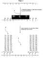
- FIG. 1is a cross-sectional view of a process scheme.
- FIG. 2is a cross-sectional view of a process scheme.
- FIG. 3is a cross sectional view of a process scheme.
- FIG. 4is a cross-sectional view of a process scheme.
- One embodimentis an article comprising: a) a substrate; b) a first metal film overlying the substrate; c) a second thin metal film overlying the first metal film; and d) a reactive organosilane covalently bonded to the upper surface of the second thin metal film through metal-oxygen-silicon bonds.
- the first metal filmmay be gold, silver, or copper and the second thin metal film may be Ti, Zr, Al, Cr, Hf. V, Ta, W, or Pb.
- the first metal filmcan generate surface plasmons and the upper surface of the second metal film is used to form chemically stable bonds to the reactive organosilane.
- the evanescent wave of the surface plasmons generated by the first metal filmextend through the second thin metal film and can be used to detect chemical changes near the upper surface of the second thin metal film. Detecting these chemical changes can be used, for example, to monitor biological molecule binding and image dielectric thin films.
- the substrateis glass or quartz. In other embodiments, the substrate comprises one face of a prism.
- the articlemay further comprise an adhesion metal layer between the substrate and the first metal film.
- the adhesion metal layertypically is Cr, Ti, W, or any combination thereof.
- the reactive organosilanehas a pattern on the surface that is a plurality of spots. In most embodiments, the spots are arranged in a microarray. Hydrophobic material may surround one or more of the reactive organosilane spots. The hydrophobic material may cause a polar liquid (e.g., water) to bead on the reactive organosilane spot, which allows the spot to be used as a microwell.
- the size of each spotis typically 10-1000 ⁇ m in diameter, and the density of spots is typically 100 to 1 million spots per square centimeter.
- the hydrophobic materialtypically comprises an inert organosilane covalently bonded to the upper surface of the second thin metal film through metal-oxygen-silicon bonds.
- the inert organosilanemay include, for example, a fluorinated alkyl group.
- the reactive organosilanecomprises hydroxy groups.
- the hydroxy groupsmay be capped with DNA or RNA (e.g., DNA or RNA have been reacted with the hydroxyl groups to form covalent bonds).
- An example of a reactive organosilanecomprises the structure
- the reactive group Rmay comprise, for example, the structures
- an inert organosilanecomprises the structure
- the reactive organosilanecomprises the structure
- hydrophobic materialcomprises the structure
- Ris a reactive group
- Xis independently at each occurrence a hydrogen or halogen
- n1-20
- q1-20.
- the reactive group Rmay be as described above.
- the distance between the upper surface of the second thin metal film and the reactive group R on the reactive organosilane, and the distance between the upper surface of the second thin metal film and the non-bonded terminus of the hydrophobic materialare controlled through the appropriate selection of alkyl (—(CH 2 ) n —), or haloalkyl (—(CX 2 ) q —, where X is a halogen) chain lengths.
- Another embodimentis a process comprising: a) depositing a first metal film on a substrate; b) depositing a second thin metal film on the first metal film; c) converting the upper surface of the second thin metal film to the corresponding metal oxide; and d) reacting a functionalized organosilane with the metal oxide, whereby a reactive organosilane is formed on the upper surface of the second thin metal film.
- the first metal film, the second thin metal film, and the substratemay be as described above.
- converting the upper surface of the second thin metal film to the corresponding metal oxidecomprises oxygen plasma treatment.
- the functionalized organosilaneis
- the reactive organosilaneis N-(2-aminoethyl)-2-aminoethyl
- the processfurther comprises patterning the reactive organosilane into a plurality of spots. In one embodiment, the process further comprises reacting the reactive organosilane with DNA or RNA.
- Another embodimentis a process comprising: a) depositing a first metal film on a substrate; b) depositing a second thin metal film on the first metal film; c) converting the upper surface of the second thin metal film to the corresponding metal oxide; d) reacting an inert organosilane on the upper surface of the second thin metal film; e) patterning the inert organosilane to give a pattern of a plurality of metal oxide spots surrounded by inert organosilane; and f) reacting a functionalized organosilane with the metal oxide, whereby a reactive organosilane is formed in the metal oxide spots on the second thin metal film.
- Another embodimentis a process comprising: a) depositing a first metal film on a substrate; b) depositing a second thin metal film on the first metal film; c) converting the upper surface of the second thin metal film to the corresponding metal oxide; d) patterning a photoresist on the upper surface into a plurality of spots, the upper surface being exposed between spots; e) reacting an inert organosilane on the metal oxide of the upper surface; f) removing the photoresist to form a plurality of metal oxide spots; and g) reacting a functionalized organosilane with the metal oxide, whereby a reactive organosilane is formed in the metal oxide spots.
- a similar embodimentis a process comprising: a) depositing a first metal film on a substrate; b) depositing second thin metal film on the first metal film; c) patterning a photoresist on the upper surface into a plurality of spots, the surface of the second thin metal film being exposed between spots; d) converting the surface of the second thin metal film between spots to a metal oxide; e) reacting an inert organosilane with the metal oxide of the second thin metal film; f) removing the photoresist to form a plurality of spots comprising the surface of the second thin metal film; g) converting the surface of the second thin metal film in the spots into a metal oxide, whereby a plurality of metal oxide spots is formed; and h) reacting a functionalized organosilane with the metal oxide spots, whereby a reactive organosilane is formed in the metal oxide spots on the second thin metal film.
- the substrate, the first metal film, and the second thin metal filmmay be as described above.
- the functionalized organosilane and the reactive organosilanemay be as described above.
- the reactive organosilaneis
- each spotis typically 10-1000 ⁇ m in diameter, and the number the density of spots is typically 100 to 1 million spots per square centimeter.
- the distance between the upper surface of the second thin metal film and the reactive group R on the reactive organosilane, and the distance between the upper surface of the second thin metal film and the non-bonded terminus of the hydrophobic materialare controlled through the appropriate selection of alkyl (—(CH 2 ) n —), or haloalkyl (—(CX 2 ) q —, where X is a halogen) chain lengths.
- Another embodimentis a method, comprising a) providing an article including: i) a substrate; ii) a first metal film overlying the substrate; iii) a second thin metal film overlying the first metal film; iv) an organosilane covalently bonded to the upper surface of the second thin metal film through metal-oxygen-silicon bonds; and v) a binding group attached to the organosilane; and b) determining whether or not the biomolecule is bound to the binding group by detecting or measuring a surface plasmon resonance signal generated from the first metal film.
- the binding groupcomprises DNA or RNA.
- the biomoleculeis typically DNA, RNA, or a protein.
- the binding groupis an antigen, an antibody, or a hapten.
- the organosilanemay have a pattern of a plurality of spots.
- the spotsmay be arranged in a microarray.
- the size of each spotis typically 10-1000 ⁇ m in diameter, and the number the density of spots is typically 100 to 1 million spots per square centimeter.
- the first metal film, the second thin metal film, and the glass substratemay be as described above.
- a glass substratewas cleaned using Diamaflow 688C.
- the substratewas soaked in a 1% solution of Diamaflow 688C in DI-water (18M ⁇ ) with and sonicated for 5 minutes. After sonication, the samples were brushed in a fresh solution of Diamaflow and DI-water and sonicated again in DI-water at 30° C. in 15 minutes.
- the substratewas rinsed for 5 minutes and dried with filtered N 2 gas. Before the metal deposition the substrate was treated with high pressure O 2 plasma for 5 minutes. The plasma cleaning process should happen right before the metal deposition otherwise the surface conditions cannot be precisely controlled.
- the metal depositionwas performed in a Denton Discovery 18 DC magnetron sputtering machine. The base pressure was less than 2 ⁇ 10 ⁇ 7 Torr.
- Argonwas used as process gas at a pressure of 7.5 mTorr during deposition.
- the magnetron currentwas set to 250 mA.
- a 2 nm thick adhesion layer of Crwas deposited followed by deposition of a 47 nm Au layer, followed by deposition of a 10 nm thick layer of Ti.
- Deposition of the inert hydrophobic organosilane and reactive organosilaneare shown schematically in cross section in FIGS. 1-2 .
- the substratewas photolithographically patterned with photoresist ( 1 ) squares (100-200 ⁇ m on one side).
- photoresist1
- O 2 -plasma treatmentwas used to enhance the bonding of the hydrophobic silane to the Ti.
- a solution of 1H,1H,2H,2H perfluoroundecyl trichlorosilanewas spin deposited, rinsed with toluene, and dried with N 2 gas. The remaining photoresist was removed using a stripper, washed with an isopropyl alcohol and DI-water rinse, and dried with filtered N 2 gas.
- the Ti surface ( 2 )was exposed as a series of spots surrounded by the hydrophobic silane ( 3 ).
- the exposed Ti surfacewas treated with O 2 plasma.
- (Glycidoxypropoxy)trimethoxysilanewas spin deposited as described above for the hydrophobic silane to give the reactive organosilane ( 4 ) patterned into series of spots, with each spot surrounded by the hydrophobic organosilane ( 3 ).
- the epoxy-reactive silanewas converted to a hydroxy-reactive silane by treatment with H 2 O/HCl ( FIG. 3 ) or ethylene glycol ( FIG. 4 ).
Landscapes
- Health & Medical Sciences (AREA)
- Immunology (AREA)
- Life Sciences & Earth Sciences (AREA)
- Engineering & Computer Science (AREA)
- Chemical & Material Sciences (AREA)
- Hematology (AREA)
- Urology & Nephrology (AREA)
- Biomedical Technology (AREA)
- Molecular Biology (AREA)
- Microbiology (AREA)
- Cell Biology (AREA)
- Biotechnology (AREA)
- Food Science & Technology (AREA)
- Medicinal Chemistry (AREA)
- Physics & Mathematics (AREA)
- Analytical Chemistry (AREA)
- Biochemistry (AREA)
- General Health & Medical Sciences (AREA)
- General Physics & Mathematics (AREA)
- Pathology (AREA)
- Inorganic Chemistry (AREA)
- Apparatus Associated With Microorganisms And Enzymes (AREA)
Abstract
Description

wherein: R is a reactive group and n=1-20. The reactive group R may comprise, for example, the structures


wherein: R is a reactive group; X is independently at each occurrence a hydrogen or halogen; n=1-20; and q=1-20. The reactive group R may be as described above. The distance between the upper surface of the second thin metal film and the reactive group R on the reactive organosilane, and the distance between the upper surface of the second thin metal film and the non-bonded terminus of the hydrophobic material are controlled through the appropriate selection of alkyl (—(CH2)n—), or haloalkyl (—(CX2)q—, where X is a halogen) chain lengths.


In some embodiments, the process further comprises patterning the reactive organosilane into a plurality of spots. In one embodiment, the process further comprises reacting the reactive organosilane with DNA or RNA.

wherein: q=1-4; and p=1-20. The functionalized organosilane and the reactive organosilane may be as described above. In one embodiment, the reactive organosilane is


The size of each spot is typically 10-1000 μm in diameter, and the number the density of spots is typically 100 to 1 million spots per square centimeter. The distance between the upper surface of the second thin metal film and the reactive group R on the reactive organosilane, and the distance between the upper surface of the second thin metal film and the non-bonded terminus of the hydrophobic material are controlled through the appropriate selection of alkyl (—(CH2)n—), or haloalkyl (—(CX2)q—, where X is a halogen) chain lengths.
Claims (45)


Priority Applications (3)
| Application Number | Priority Date | Filing Date | Title |
|---|---|---|---|
| US11/296,659US7463358B2 (en) | 2005-12-06 | 2005-12-06 | Highly stable surface plasmon resonance plates, microarrays, and methods |
| US12/330,384US8094315B2 (en) | 2005-12-06 | 2008-12-08 | Methods for making and using SPR microarrays |
| US13/337,506US20120115748A1 (en) | 2005-12-06 | 2011-12-27 | Methods for making and using spr microarrays |
Applications Claiming Priority (1)
| Application Number | Priority Date | Filing Date | Title |
|---|---|---|---|
| US11/296,659US7463358B2 (en) | 2005-12-06 | 2005-12-06 | Highly stable surface plasmon resonance plates, microarrays, and methods |
Related Child Applications (1)
| Application Number | Title | Priority Date | Filing Date |
|---|---|---|---|
| US12/330,384DivisionUS8094315B2 (en) | 2005-12-06 | 2008-12-08 | Methods for making and using SPR microarrays |
Publications (2)
| Publication Number | Publication Date |
|---|---|
| US20070128455A1 US20070128455A1 (en) | 2007-06-07 |
| US7463358B2true US7463358B2 (en) | 2008-12-09 |
Family
ID=38119131
Family Applications (3)
| Application Number | Title | Priority Date | Filing Date |
|---|---|---|---|
| US11/296,659Active2026-05-28US7463358B2 (en) | 2005-12-06 | 2005-12-06 | Highly stable surface plasmon resonance plates, microarrays, and methods |
| US12/330,384Active2026-10-20US8094315B2 (en) | 2005-12-06 | 2008-12-08 | Methods for making and using SPR microarrays |
| US13/337,506AbandonedUS20120115748A1 (en) | 2005-12-06 | 2011-12-27 | Methods for making and using spr microarrays |
Family Applications After (2)
| Application Number | Title | Priority Date | Filing Date |
|---|---|---|---|
| US12/330,384Active2026-10-20US8094315B2 (en) | 2005-12-06 | 2008-12-08 | Methods for making and using SPR microarrays |
| US13/337,506AbandonedUS20120115748A1 (en) | 2005-12-06 | 2011-12-27 | Methods for making and using spr microarrays |
Country Status (1)
| Country | Link |
|---|---|
| US (3) | US7463358B2 (en) |
Cited By (8)
| Publication number | Priority date | Publication date | Assignee | Title |
|---|---|---|---|---|
| US20040258832A1 (en)* | 2003-06-17 | 2004-12-23 | Barklund Anna M. | Method of chemical analysis using microwells patterned from self-assembled monolayers and substrates |
| US20060134669A1 (en)* | 2004-11-19 | 2006-06-22 | Casasanta Vincenzo Iii | Plasmon resonance biosensor and method |
| US20090060787A1 (en)* | 2007-08-29 | 2009-03-05 | Gibum Kim | Method for uniform analyte fluid delivery to microarrays |
| US20090262356A1 (en)* | 2008-03-27 | 2009-10-22 | Plexera, Llc | User interface and method for using an spr system |
| US7889347B2 (en) | 2005-11-21 | 2011-02-15 | Plexera Llc | Surface plasmon resonance spectrometer with an actuator driven angle scanning mechanism |
| US8004669B1 (en) | 2007-12-18 | 2011-08-23 | Plexera Llc | SPR apparatus with a high performance fluid delivery system |
| US8094315B2 (en) | 2005-12-06 | 2012-01-10 | Plexera Llc | Methods for making and using SPR microarrays |
| US8263377B2 (en) | 2007-04-03 | 2012-09-11 | Plexera, Llc | Label free kinase assays and reagents |
Families Citing this family (4)
| Publication number | Priority date | Publication date | Assignee | Title |
|---|---|---|---|---|
| US20090060786A1 (en)* | 2007-08-29 | 2009-03-05 | Gibum Kim | Microfluidic apparatus for wide area microarrays |
| JP4572244B2 (en)* | 2008-04-09 | 2010-11-04 | シャープ株式会社 | Surface plasmon sensor |
| CN104374746A (en)* | 2014-10-27 | 2015-02-25 | 李博 | Method for preparing surface plasma resonance chip by taking silver as target |
| WO2023049192A1 (en)* | 2021-09-22 | 2023-03-30 | Ultima Genomics, Inc. | Methods and systems for substrate functionalization |
Citations (22)
| Publication number | Priority date | Publication date | Assignee | Title |
|---|---|---|---|---|
| US5445934A (en) | 1989-06-07 | 1995-08-29 | Affymax Technologies N.V. | Array of oligonucleotides on a solid substrate |
| US6040193A (en) | 1991-11-22 | 2000-03-21 | Affymetrix, Inc. | Combinatorial strategies for polymer synthesis |
| US6054270A (en) | 1988-05-03 | 2000-04-25 | Oxford Gene Technology Limited | Analying polynucleotide sequences |
| US6150147A (en) | 1998-02-06 | 2000-11-21 | Affymetrix, Inc. | Biological array fabrication methods with reduction of static charge |
| US6218111B1 (en) | 1993-07-30 | 2001-04-17 | Oxford Gene Technology Limited | Tag reagent and assay method |
| US6309831B1 (en) | 1998-02-06 | 2001-10-30 | Affymetrix, Inc. | Method of manufacturing biological chips |
| US6346413B1 (en) | 1989-06-07 | 2002-02-12 | Affymetrix, Inc. | Polymer arrays |
| US6399365B2 (en) | 1994-06-08 | 2002-06-04 | Affymetrix, Inc. | Bioarray chip reaction apparatus and its manufacture |
| WO2002052260A2 (en)* | 2000-12-22 | 2002-07-04 | Jandratek Gmbh | Biosensor and method of producing the same |
| US6416952B1 (en) | 1989-06-07 | 2002-07-09 | Affymetrix, Inc. | Photolithographic and other means for manufacturing arrays |
| US20030100004A1 (en) | 2001-11-27 | 2003-05-29 | Markus Kurz | Solid-phase immobilization of proteins and peptides |
| US6576424B2 (en) | 1989-06-07 | 2003-06-10 | Affymetrix Inc. | Arrays and methods for detecting nucleic acids |
| US20030107741A1 (en)* | 2001-12-11 | 2003-06-12 | Pyo Hyeon Bong | Surface plasmon resonance sensor system |
| US6600031B1 (en) | 1989-06-07 | 2003-07-29 | Affymetrix, Inc. | Methods of making nucleic acid or oligonucleotide arrays |
| US20030143576A1 (en) | 2001-08-22 | 2003-07-31 | Heman Chao | Method and device for integrated protein expression, purification and detection |
| US6610482B1 (en) | 1989-06-07 | 2003-08-26 | Affymetrix, Inc. | Support bound probes and methods of analysis using the same |
| US20040043384A1 (en) | 2002-08-28 | 2004-03-04 | Oleinikov Andrew V. | In vitro protein translation microarray device |
| US20040161748A1 (en) | 2000-08-15 | 2004-08-19 | Mingyue He | Functional protein arrays |
| US6789040B2 (en) | 2000-08-22 | 2004-09-07 | Affymetrix, Inc. | System, method, and computer software product for specifying a scanning area of a substrate |
| US6800453B2 (en) | 2001-01-23 | 2004-10-05 | President And Fellows Of Harvard College | Nucleic-acid programmable protein arrays |
| US20040198637A1 (en) | 2002-12-22 | 2004-10-07 | The Scripps Research Institute | Protein arrays |
| US6806361B1 (en) | 2000-03-17 | 2004-10-19 | Affymetrix, Inc. | Methods of enhancing functional performance of nucleic acid arrays |
Family Cites Families (164)
| Publication number | Priority date | Publication date | Assignee | Title |
|---|---|---|---|---|
| US3105902A (en) | 1960-09-19 | 1963-10-01 | Standard Oil Co | Controlled atmosphere X-ray diffraction spectrometer |
| US3751587A (en)* | 1972-01-20 | 1973-08-07 | Saxon Ind Inc | Laser printing system |
| US3891507A (en)* | 1974-05-30 | 1975-06-24 | American Cyanamid Co | Organ function test cards |
| US4038030A (en)* | 1975-04-10 | 1977-07-26 | American Hospital Supply Corporation | Profile analysis pack and method |
| US3990850A (en) | 1976-01-06 | 1976-11-09 | Akzona Incorporated | Diagnostic test card |
| US4148057A (en)* | 1977-10-25 | 1979-04-03 | Solution Sciences, Inc. | Direct laser printing and forming apparatus |
| US4375025A (en)* | 1980-06-19 | 1983-02-22 | Automated Industrial Systems, Inc. | Laser strip marker |
| US4585931A (en)* | 1983-11-21 | 1986-04-29 | At&T Technologies, Inc. | Method for automatically identifying semiconductor wafers |
| GB8417301D0 (en)* | 1984-07-06 | 1984-08-08 | Serono Diagnostics Ltd | Assay |
| US4707722A (en) | 1984-12-17 | 1987-11-17 | Motorola, Inc. | Laser marking method and ablative coating for use therein |
| US4753863A (en)* | 1985-02-01 | 1988-06-28 | Motorola Inc. | Laser markable molding compound |
| US4740468A (en)* | 1985-02-14 | 1988-04-26 | Syntex (U.S.A.) Inc. | Concentrating immunochemical test device and method |
| US4638144A (en)* | 1985-04-24 | 1987-01-20 | Automated Industrial Systems | Indexing laser marker |
| JPS6234920A (en)* | 1985-08-07 | 1987-02-14 | Toshiba Corp | Epoxy resin composition and resin-encapsulated semiconductor device produced by using same |
| EP0215669A3 (en) | 1985-09-17 | 1989-08-30 | Seiko Instruments Inc. | Analytical device and method for analysis of biochemicals, microbes and cells |
| KR910000826B1 (en) | 1986-11-14 | 1991-02-09 | 미쓰비시덴기 가부시기가이샤 | Method of laser marking |
| US5225047A (en)* | 1987-01-20 | 1993-07-06 | Weyerhaeuser Company | Crosslinked cellulose products and method for their preparation |
| US5192507A (en)* | 1987-06-05 | 1993-03-09 | Arthur D. Little, Inc. | Receptor-based biosensors |
| DE3852036T2 (en)* | 1987-07-27 | 1995-03-09 | Commonwealth Scientific And Industrial Research Organization, Campbell | RECEPTOR MEMBRANES. |
| CA1321488C (en)* | 1987-08-22 | 1993-08-24 | Martin Francis Finlan | Biological sensors |
| DE3731835A1 (en) | 1987-09-22 | 1989-03-30 | Siemens Ag | LASER BEAM INDUCED COLOR PRINTING |
| EP0315790B1 (en)* | 1987-10-13 | 1992-04-15 | Taiyo Yuden Co., Ltd. | Chemical sensors and their divided parts |
| SE462408B (en)* | 1988-11-10 | 1990-06-18 | Pharmacia Ab | OPTICAL BIOSENSOR SYSTEM USING SURFACE MONITORING RESONSE FOR THE DETECTION OF A SPECIFIC BIOMOLIC CYCLE, TO CALIBRATE THE SENSOR DEVICE AND TO CORRECT FOUND BASELINE OPERATION IN THE SYSTEM |
| SE8804074D0 (en)* | 1988-11-10 | 1988-11-10 | Pharmacia Ab | SENSOR UNIT AND ITS USE IN BIOSENSOR SYSTEM |
| JPH02133185A (en)* | 1988-11-10 | 1990-05-22 | Mitsubishi Electric Corp | Laser marking method for semiconductor devices |
| SE462454B (en)* | 1988-11-10 | 1990-06-25 | Pharmacia Ab | METHOD FOR USE IN BIOSENSORS |
| US5200051A (en)* | 1988-11-14 | 1993-04-06 | I-Stat Corporation | Wholly microfabricated biosensors and process for the manufacture and use thereof |
| US5089112A (en)* | 1989-03-20 | 1992-02-18 | Associated Universities, Inc. | Electrochemical biosensor based on immobilized enzymes and redox polymers |
| DK0418355T3 (en) | 1989-04-04 | 1994-09-12 | Urban Gerald | Method for immobilizing proteins, peptides, coenzymes, etc. on a substrate |
| DE59002516D1 (en)* | 1989-04-06 | 1993-10-07 | Ciba Geigy | Laser marking of ceramic materials, glazes, ceramic glasses and glasses. |
| US5116481A (en)* | 1989-04-07 | 1992-05-26 | Hitachi, Ltd. | Anion-selective, sensitive film, electrode containing the same and the use thereof |
| US5491097A (en)* | 1989-06-15 | 1996-02-13 | Biocircuits Corporation | Analyte detection with multilayered bioelectronic conductivity sensors |
| US5268305A (en) | 1989-06-15 | 1993-12-07 | Biocircuits Corporation | Multi-optical detection system |
| US5368712A (en) | 1989-11-02 | 1994-11-29 | Synporin Technologies, Inc. | Biologically mimetic synthetic ion channel transducers |
| US5068124A (en) | 1989-11-17 | 1991-11-26 | International Business Machines Corporation | Method for depositing high quality silicon dioxide by pecvd |
| US5104619A (en)* | 1990-01-24 | 1992-04-14 | Gds Technology, Inc. | Disposable diagnostic system |
| GB9005872D0 (en)* | 1990-03-15 | 1990-05-09 | British Aerospace | A laser markable white pigment composition |
| US5105941A (en)* | 1990-04-05 | 1992-04-21 | Chicago Tribune Company | Sample packet newspaper insert |
| US5478756A (en) | 1990-07-24 | 1995-12-26 | Fisons Plc | Chemical sensor for detecting binding reactions |
| DE69130962T2 (en) | 1990-11-07 | 1999-10-28 | Teijin Ltd., Osaka | Polyester resin composition |
| US5401378A (en)* | 1991-03-27 | 1995-03-28 | Australian Membrane & Biotechnology Research Institute | Ionic reservoir at electrode surface |
| US6111645A (en)* | 1991-04-29 | 2000-08-29 | Massachusetts Institute Of Technology | Grating based phase control optical delay line |
| US5474796A (en) | 1991-09-04 | 1995-12-12 | Protogene Laboratories, Inc. | Method and apparatus for conducting an array of chemical reactions on a support surface |
| JP2862413B2 (en) | 1991-10-02 | 1999-03-03 | ポリプラスチックス株式会社 | Laser marking method |
| JPH07508342A (en)* | 1992-04-22 | 1995-09-14 | エコール ポリテクニーク フェデラル ドゥ ローザンヌ(エーペーエフエル) | lipid membrane sensor |
| JP3102822B2 (en) | 1992-05-29 | 2000-10-23 | 日本ジーイープラスチックス株式会社 | Resin composition for laser marking |
| US5736410A (en)* | 1992-09-14 | 1998-04-07 | Sri International | Up-converting reporters for biological and other assays using laser excitation techniques |
| US5445923A (en) | 1992-09-30 | 1995-08-29 | Somar Corporation | Laser beam absorbing resin composition and laser beam marking method |
| EP1130388A1 (en)* | 1992-10-01 | 2001-09-05 | Australian Membrane And Biotechnology Research Institute | Improved sensor membranes |
| JP2751089B2 (en)* | 1992-11-30 | 1998-05-18 | 大日本インキ化学工業株式会社 | Laser marking method and printing ink |
| JPH0810729B2 (en) | 1993-01-20 | 1996-01-31 | 日本電気株式会社 | Stamping machine |
| DE4303860C2 (en)* | 1993-02-10 | 1995-11-09 | Draegerwerk Ag | Carrier for colorimetric gas detection in composite film construction |
| US5329090A (en)* | 1993-04-09 | 1994-07-12 | A B Lasers, Inc. | Writing on silicon wafers |
| US5512492A (en) | 1993-05-18 | 1996-04-30 | University Of Utah Research Foundation | Waveguide immunosensor with coating chemistry providing enhanced sensitivity |
| CA2163426C (en)* | 1993-05-28 | 2005-11-01 | T. William Hutchens | Method and apparatus for desorption and ionization of analytes |
| US6020208A (en)* | 1994-05-27 | 2000-02-01 | Baylor College Of Medicine | Systems for surface-enhanced affinity capture for desorption and detection of analytes |
| WO1995006240A1 (en) | 1993-08-24 | 1995-03-02 | Metrika Laboratories, Inc. | Novel disposable electronic assay device |
| US5512131A (en)* | 1993-10-04 | 1996-04-30 | President And Fellows Of Harvard College | Formation of microstamped patterns on surfaces and derivative articles |
| US5629790A (en)* | 1993-10-18 | 1997-05-13 | Neukermans; Armand P. | Micromachined torsional scanner |
| US5470952A (en) | 1993-10-20 | 1995-11-28 | Regeneron Pharmaceuticals, Inc. | CNTF and IL-6 antagonists |
| US5527711A (en)* | 1993-12-13 | 1996-06-18 | Hewlett Packard Company | Method and reagents for binding chemical analytes to a substrate surface, and related analytical devices and diagnostic techniques |
| IL108726A (en) | 1994-02-22 | 1999-12-31 | Yissum Res Dev Co | Electrobiochemical method and system for the determination of an analyte which is a member of a recognition pair in a liquid medium and electrodes therefor |
| US5536822A (en)* | 1994-03-09 | 1996-07-16 | University Of Virginia Alumni Patents Foundation | γ-phosphate linked adenosine 5' triphosphate sepharose |
| FR2720832A1 (en) | 1994-04-22 | 1995-12-08 | Francis Garnier | Electroactive electrodes and membranes based on bioactive peptides, for the recognition, extraction or release of biologically active species. |
| US5824483A (en) | 1994-05-18 | 1998-10-20 | Pence Inc. | Conformationally-restricted combinatiorial library composition and method |
| US5514501A (en)* | 1994-06-07 | 1996-05-07 | The United States Of America As Represented By The Secretary Of Commerce | Process for UV-photopatterning of thiolate monolayers self-assembled on gold, silver and other substrates |
| EP0690306A1 (en)* | 1994-06-28 | 1996-01-03 | Mochida Pharmaceutical Co., Ltd. | Method and device for specific binding assay |
| US5485277A (en)* | 1994-07-26 | 1996-01-16 | Physical Optics Corporation | Surface plasmon resonance sensor and methods for the utilization thereof |
| DE4430023A1 (en) | 1994-08-24 | 1996-02-29 | Boehringer Mannheim Gmbh | Electrochemical sensor |
| US5624537A (en)* | 1994-09-20 | 1997-04-29 | The University Of British Columbia - University-Industry Liaison Office | Biosensor and interface membrane |
| SE9403245D0 (en)* | 1994-09-26 | 1994-09-26 | Pharmacia Biosensor Ab | Improvements relating to bilayer lipid membranes |
| US5688642A (en) | 1994-12-01 | 1997-11-18 | The United States Of America As Represented By The Secretary Of The Navy | Selective attachment of nucleic acid molecules to patterned self-assembled surfaces |
| US5567301A (en) | 1995-03-01 | 1996-10-22 | Illinois Institute Of Technology | Antibody covalently bound film immunobiosensor |
| US5798030A (en) | 1995-05-17 | 1998-08-25 | Australian Membrane And Biotechnology Research Institute | Biosensor membranes |
| US5690894A (en) | 1995-05-23 | 1997-11-25 | The Regents Of The University Of California | High density array fabrication and readout method for a fiber optic biosensor |
| AUPN366995A0 (en) | 1995-06-20 | 1995-07-13 | Australian Membrane And Biotechnology Research Institute | Self-assembly of bilayer membrane sensors |
| IT1275482B (en)* | 1995-07-05 | 1997-08-07 | Cooperativa Centro Ricerche Po | ELECTROCHEMICAL BIOSENSORS BASED ON COMPOSITE TRANSDUCERS |
| US5838361A (en) | 1996-01-11 | 1998-11-17 | Micron Technology, Inc. | Laser marking techniques |
| GB9602542D0 (en)* | 1996-02-08 | 1996-04-10 | Fisons Plc | Analytical device |
| US6586193B2 (en) | 1996-04-25 | 2003-07-01 | Genicon Sciences Corporation | Analyte assay using particulate labels |
| US6165335A (en) | 1996-04-25 | 2000-12-26 | Pence And Mcgill University | Biosensor device and method |
| US5955379A (en) | 1996-04-25 | 1999-09-21 | Mcgill University | Biosensor device and method |
| US5938595A (en) | 1996-05-24 | 1999-08-17 | The Regents Of The University Of California | Fiber optic D dimer biosensor |
| US5707502A (en)* | 1996-07-12 | 1998-01-13 | Chiron Diagnostics Corporation | Sensors for measuring analyte concentrations and methods of making same |
| US5832165A (en)* | 1996-08-28 | 1998-11-03 | University Of Utah Research Foundation | Composite waveguide for solid phase binding assays |
| US6024925A (en)* | 1997-01-23 | 2000-02-15 | Sequenom, Inc. | Systems and methods for preparing low volume analyte array elements |
| WO1998022625A1 (en)* | 1996-11-20 | 1998-05-28 | The Regents Of The University Of Michigan | Microfabricated isothermal nucleic acid amplification devices and methods |
| SE9700384D0 (en) | 1997-02-04 | 1997-02-04 | Biacore Ab | Analytical method and apparatus |
| US6406845B1 (en) | 1997-05-05 | 2002-06-18 | Trustees Of Tuft College | Fiber optic biosensor for selectively detecting oligonucleotide species in a mixed fluid sample |
| NZ516848A (en) | 1997-06-20 | 2004-03-26 | Ciphergen Biosystems Inc | Retentate chromatography apparatus with applications in biology and medicine |
| US6245506B1 (en) | 1997-07-30 | 2001-06-12 | Bbi Bioseq, Inc. | Integrated sequencing device |
| US6207370B1 (en) | 1997-09-02 | 2001-03-27 | Sequenom, Inc. | Diagnostics based on mass spectrometric detection of translated target polypeptides |
| US5922617A (en)* | 1997-11-12 | 1999-07-13 | Functional Genetics, Inc. | Rapid screening assay methods and devices |
| US6101946A (en) | 1997-11-21 | 2000-08-15 | Telechem International Inc. | Microarray printing device including printing pins with flat tips and exterior channel and method of manufacture |
| JP3437170B2 (en) | 1997-12-12 | 2003-08-18 | ピーイー コーポレイション (エヌワイ) | Optical resonance analysis system |
| US6232066B1 (en)* | 1997-12-19 | 2001-05-15 | Neogen, Inc. | High throughput assay system |
| US6074616A (en)* | 1998-01-05 | 2000-06-13 | Biosite Diagnostics, Inc. | Media carrier for an assay device |
| JP4387588B2 (en)* | 1998-02-04 | 2009-12-16 | メルク エンド カムパニー インコーポレーテッド | Virtual wells for high-throughput screening assays |
| US6406921B1 (en) | 1998-07-14 | 2002-06-18 | Zyomyx, Incorporated | Protein arrays for high-throughput screening |
| US6197599B1 (en) | 1998-07-30 | 2001-03-06 | Guorong Chin | Method to detect proteins |
| US6937221B2 (en)* | 1998-08-05 | 2005-08-30 | Microvision, Inc. | Scanned beam display |
| US6380365B1 (en)* | 1998-09-04 | 2002-04-30 | Affitech As | Temperature dependent ligand facilitated purification of proteins |
| FR2783179B1 (en)* | 1998-09-16 | 2000-10-06 | Commissariat Energie Atomique | CHEMICAL OR BIOLOGICAL ANALYSIS DEVICE COMPRISING A PLURALITY OF ANALYSIS SITES ON A MEDIUM, AND ITS MANUFACTURING METHOD |
| US6472179B2 (en) | 1998-09-25 | 2002-10-29 | Regeneron Pharmaceuticals, Inc. | Receptor based antagonists and methods of making and using |
| AU1717600A (en)* | 1998-11-10 | 2000-05-29 | Biocrystal Limited | Methods for identification and verification |
| AU2898500A (en) | 1999-03-02 | 2000-09-21 | Helix Biopharma Corporation | Biosensor device and method |
| US6489102B2 (en)* | 1999-08-05 | 2002-12-03 | Wisconsin Alumni Research Foundation | Biomolecule and/or cellular arrays on metal surfaces and product produced thereby |
| US6433907B1 (en) | 1999-08-05 | 2002-08-13 | Microvision, Inc. | Scanned display with plurality of scanning assemblies |
| US6362912B1 (en)* | 1999-08-05 | 2002-03-26 | Microvision, Inc. | Scanned imaging apparatus with switched feeds |
| US6245590B1 (en)* | 1999-08-05 | 2001-06-12 | Microvision Inc. | Frequency tunable resonant scanner and method of making |
| US6558623B1 (en)* | 2000-07-06 | 2003-05-06 | Robodesign International, Inc. | Microarray dispensing with real-time verification and inspection |
| US6448089B1 (en) | 1999-10-12 | 2002-09-10 | Aurora Biosciences Corporation | Multiwell scanner and scanning method |
| US6219138B1 (en)* | 2000-01-10 | 2001-04-17 | The United States Of America As Represented By The Secretary Of The Navy | Particle sizing technique |
| EP1399180A4 (en)* | 2000-02-29 | 2004-04-07 | Progenics Pharm Inc | CCR5 SULPHATE PEPTIDES FOR THE TREATMENT OF HIV-1 INFECTION |
| US6489106B1 (en) | 2000-03-10 | 2002-12-03 | Nec Research Institute, Inc. | Control of the expression of anchored genes using micron scale heaters |
| US6447723B1 (en) | 2000-03-13 | 2002-09-10 | Packard Instrument Company, Inc. | Microarray spotting instruments incorporating sensors and methods of using sensors for improving performance of microarray spotting instruments |
| AU2001242927A1 (en) | 2000-03-14 | 2001-09-24 | Institutet Polymerutveckling Ab | Improved imaging spr apparatus |
| AU2001249141A1 (en)* | 2000-03-17 | 2001-10-03 | Dow Global Technologies Inc. | Polyolefin foam for sound and thermal insulation |
| US7126688B2 (en) | 2000-07-11 | 2006-10-24 | Maven Technologies, Llc | Microarray scanning |
| EP2189783A1 (en) | 2000-08-09 | 2010-05-26 | Artificial Sensing Instruments ASI AG | Waveguide grid structure and optical measuring assembly |
| US6545758B1 (en)* | 2000-08-17 | 2003-04-08 | Perry Sandstrom | Microarray detector and synthesizer |
| EP1328346A2 (en)* | 2000-10-06 | 2003-07-23 | Protasis Corporation | Microfluidic substrate assembly and method for making same |
| US7094595B2 (en) | 2000-10-30 | 2006-08-22 | Sru Biosystems, Inc. | Label-free high-throughput optical technique for detecting biomolecular interactions |
| EP2465943A3 (en) | 2001-03-16 | 2012-10-03 | Kalim Mir | Linear polymer display |
| US6885454B2 (en) | 2001-03-28 | 2005-04-26 | Fuji Photo Film Co., Ltd. | Measuring apparatus |
| US6862398B2 (en)* | 2001-03-30 | 2005-03-01 | Texas Instruments Incorporated | System for directed molecular interaction in surface plasmon resonance analysis |
| US20020197729A1 (en) | 2001-06-21 | 2002-12-26 | Fuji Photo Film Co., Ltd. | Biochemical analysis unit and method for manufacturing the same |
| US6485918B1 (en) | 2001-07-02 | 2002-11-26 | Packard Bioscience Corporation | Method and apparatus for incubation of a liquid reagent and target spots on a microarray substrate |
| GB0119062D0 (en) | 2001-08-06 | 2001-09-26 | Cambridge Consultants | Interferometer |
| JP4157037B2 (en) | 2001-09-21 | 2008-09-24 | オリンパス株式会社 | Defect inspection equipment |
| US7300798B2 (en)* | 2001-10-18 | 2007-11-27 | Agilent Technologies, Inc. | Chemical arrays |
| GR1004178B (en)* | 2001-11-29 | 2003-03-05 | "����������" | Integrated optoelectronic silicon biosensor for the detection of biomolecules labeled with chromophore groups or nanoparticles |
| US7041208B2 (en)* | 2001-12-11 | 2006-05-09 | Sau Lan Tang Staats | Microfluidic devices and methods for two-dimensional separations |
| EP1474504A2 (en)* | 2002-01-24 | 2004-11-10 | Pointilliste, Inc. | Use of collections of binding sites for sample profiling and other applications |
| US20040014946A1 (en)* | 2002-04-25 | 2004-01-22 | Heman Chao | Protein interaction method and composition |
| US7064827B2 (en)* | 2002-05-20 | 2006-06-20 | Brown University Research Foundation | Optical tracking and detection of particles by solid state energy sources |
| WO2004001402A1 (en) | 2002-06-21 | 2003-12-31 | Olympus Corporation | Biomolecule analyzer |
| US20040067597A1 (en)* | 2002-07-31 | 2004-04-08 | Caliper Technologies Corp. | High density reagent array preparation methods |
| AU2004204502B2 (en) | 2003-01-13 | 2008-05-29 | The Regents Of The University Of Michigan | Method to form a protein microarray system |
| JP3856763B2 (en)* | 2003-03-11 | 2006-12-13 | 財団法人川村理化学研究所 | Manufacturing method of microfluidic device |
| JP3775677B2 (en)* | 2003-05-07 | 2006-05-17 | 船井電機株式会社 | MEMS mirror device and optical disk device |
| US7373255B2 (en) | 2003-06-06 | 2008-05-13 | Biacore Ab | Method and system for determination of molecular interaction parameters |
| US20040258832A1 (en) | 2003-06-17 | 2004-12-23 | Barklund Anna M. | Method of chemical analysis using microwells patterned from self-assembled monolayers and substrates |
| US7576862B2 (en)* | 2003-08-26 | 2009-08-18 | Blueshift Biotechnologies, Inc. | Measuring time dependent fluorescence |
| US20050095577A1 (en)* | 2003-10-31 | 2005-05-05 | Yang Dan-Hui D. | Protein bioarray on silane-modified substrate surface |
| CN100538338C (en) | 2003-12-26 | 2009-09-09 | 松下电器产业株式会社 | The analytical approach of the part in the sample and the device of the part in the analytical sample |
| JP4616567B2 (en) | 2004-03-11 | 2011-01-19 | 株式会社堀場製作所 | Measuring method, analyzing method, measuring device, analyzing device, ellipsometer and computer program |
| WO2006014326A1 (en)* | 2004-07-02 | 2006-02-09 | Lumera Corporation | Fiber optic bio-sensor |
| US7745143B2 (en) | 2004-11-19 | 2010-06-29 | Plexera, Llc | Plasmon resonance biosensor and method |
| US7445887B2 (en)* | 2005-01-07 | 2008-11-04 | Fortebio, Inc. | Enzyme activity measurements using bio-layer interferometry |
| KR100668323B1 (en) | 2005-01-19 | 2007-01-12 | 삼성전자주식회사 | Portable Biochip Scanner Using Surface Plasmon Resonance |
| US20060234265A1 (en) | 2005-03-21 | 2006-10-19 | Jim Richey | Microarrays having multi-functional, compartmentalized analysis areas and methods of use |
| US20070081163A1 (en)* | 2005-06-03 | 2007-04-12 | Minhua Liang | Method and apparatus for scanned beam microarray assay |
| US20070139653A1 (en) | 2005-06-07 | 2007-06-21 | Guan Hann W | MEMS Micromirror Surface Plasmon Resonance Biosensor and Method |
| JP4671346B2 (en)* | 2005-09-13 | 2011-04-13 | キヤノン株式会社 | Biochemical reaction cassette with improved liquid filling |
| US20070099180A1 (en)* | 2005-10-31 | 2007-05-03 | Robotti Karla M | Evanescent wave sensor with attached ligand |
| WO2007061981A2 (en) | 2005-11-21 | 2007-05-31 | Lumera Corporation | Surface plasmon resonance spectrometer with an actuator-driven angle scanning mechanism |
| US7463358B2 (en)* | 2005-12-06 | 2008-12-09 | Lumera Corporation | Highly stable surface plasmon resonance plates, microarrays, and methods |
| US20070140918A1 (en)* | 2005-12-19 | 2007-06-21 | Hongfeng Yin | Fluidic separation devices and methods with reduced sample broadening |
| SE531493C2 (en)* | 2006-10-31 | 2009-04-28 | Knut Johansen | Sensor |
| US7695976B2 (en) | 2007-08-29 | 2010-04-13 | Plexera Bioscience, Llc | Method for uniform analyte fluid delivery to microarrays |
| US20090060786A1 (en) | 2007-08-29 | 2009-03-05 | Gibum Kim | Microfluidic apparatus for wide area microarrays |
| WO2009149125A2 (en)* | 2008-06-02 | 2009-12-10 | Life Technologies Corporation | Localization of near-field resonances in bowtie antennae: influence of adhesion layers |
| WO2010037227A1 (en)* | 2008-09-30 | 2010-04-08 | Université de Montréal | High resolution surface plasmon resonance instrument using a dove prism |
- 2005
- 2005-12-06USUS11/296,659patent/US7463358B2/enactiveActive
- 2008
- 2008-12-08USUS12/330,384patent/US8094315B2/enactiveActive
- 2011
- 2011-12-27USUS13/337,506patent/US20120115748A1/ennot_activeAbandoned
Patent Citations (28)
| Publication number | Priority date | Publication date | Assignee | Title |
|---|---|---|---|---|
| US6054270A (en) | 1988-05-03 | 2000-04-25 | Oxford Gene Technology Limited | Analying polynucleotide sequences |
| US6416952B1 (en) | 1989-06-07 | 2002-07-09 | Affymetrix, Inc. | Photolithographic and other means for manufacturing arrays |
| US6346413B1 (en) | 1989-06-07 | 2002-02-12 | Affymetrix, Inc. | Polymer arrays |
| US6610482B1 (en) | 1989-06-07 | 2003-08-26 | Affymetrix, Inc. | Support bound probes and methods of analysis using the same |
| US6600031B1 (en) | 1989-06-07 | 2003-07-29 | Affymetrix, Inc. | Methods of making nucleic acid or oligonucleotide arrays |
| US6225625B1 (en) | 1989-06-07 | 2001-05-01 | Affymetrix, Inc. | Signal detection methods and apparatus |
| US6261776B1 (en) | 1989-06-07 | 2001-07-17 | Affymetrix, Inc. | Nucleic acid arrays |
| US6291183B1 (en) | 1989-06-07 | 2001-09-18 | Affymetrix, Inc. | Very large scale immobilized polymer synthesis |
| US6491871B1 (en) | 1989-06-07 | 2002-12-10 | Affymetrix, Inc. | System for determining receptor-ligand binding affinity |
| US6576424B2 (en) | 1989-06-07 | 2003-06-10 | Affymetrix Inc. | Arrays and methods for detecting nucleic acids |
| US5445934A (en) | 1989-06-07 | 1995-08-29 | Affymax Technologies N.V. | Array of oligonucleotides on a solid substrate |
| US6040193A (en) | 1991-11-22 | 2000-03-21 | Affymetrix, Inc. | Combinatorial strategies for polymer synthesis |
| US6576426B2 (en) | 1993-07-30 | 2003-06-10 | Oxford Gene Technology Limited | Tag reagent and assay method |
| US6218111B1 (en) | 1993-07-30 | 2001-04-17 | Oxford Gene Technology Limited | Tag reagent and assay method |
| US6733977B2 (en) | 1994-06-08 | 2004-05-11 | Affymetrix, Inc. | Hybridization device and method |
| US6399365B2 (en) | 1994-06-08 | 2002-06-04 | Affymetrix, Inc. | Bioarray chip reaction apparatus and its manufacture |
| US6309831B1 (en) | 1998-02-06 | 2001-10-30 | Affymetrix, Inc. | Method of manufacturing biological chips |
| US6150147A (en) | 1998-02-06 | 2000-11-21 | Affymetrix, Inc. | Biological array fabrication methods with reduction of static charge |
| US6806361B1 (en) | 2000-03-17 | 2004-10-19 | Affymetrix, Inc. | Methods of enhancing functional performance of nucleic acid arrays |
| US20040161748A1 (en) | 2000-08-15 | 2004-08-19 | Mingyue He | Functional protein arrays |
| US6789040B2 (en) | 2000-08-22 | 2004-09-07 | Affymetrix, Inc. | System, method, and computer software product for specifying a scanning area of a substrate |
| WO2002052260A2 (en)* | 2000-12-22 | 2002-07-04 | Jandratek Gmbh | Biosensor and method of producing the same |
| US6800453B2 (en) | 2001-01-23 | 2004-10-05 | President And Fellows Of Harvard College | Nucleic-acid programmable protein arrays |
| US20030143576A1 (en) | 2001-08-22 | 2003-07-31 | Heman Chao | Method and device for integrated protein expression, purification and detection |
| US20030100004A1 (en) | 2001-11-27 | 2003-05-29 | Markus Kurz | Solid-phase immobilization of proteins and peptides |
| US20030107741A1 (en)* | 2001-12-11 | 2003-06-12 | Pyo Hyeon Bong | Surface plasmon resonance sensor system |
| US20040043384A1 (en) | 2002-08-28 | 2004-03-04 | Oleinikov Andrew V. | In vitro protein translation microarray device |
| US20040198637A1 (en) | 2002-12-22 | 2004-10-07 | The Scripps Research Institute | Protein arrays |
Non-Patent Citations (3)
| Title |
|---|
| "Surface Plasmon Resonance (SPR)," BMS, http://www.bmskorea.co.kr/bms-Product/bms-Product-Main.aspx?sec=detail&num=28211, printed Nov. 15, 2005, 6 pages. |
| Hyun et al., "Enzymatic Nanolithography of a Self-Assembled Oligonucleotide Monolayer on Gold," J. Am. Chem. Soc., 2004, 126:4770-4771. |
| Machine translation of DE 10064146.* |
Cited By (15)
| Publication number | Priority date | Publication date | Assignee | Title |
|---|---|---|---|---|
| US20040258832A1 (en)* | 2003-06-17 | 2004-12-23 | Barklund Anna M. | Method of chemical analysis using microwells patterned from self-assembled monolayers and substrates |
| US7745143B2 (en) | 2004-11-19 | 2010-06-29 | Plexera, Llc | Plasmon resonance biosensor and method |
| US20060134669A1 (en)* | 2004-11-19 | 2006-06-22 | Casasanta Vincenzo Iii | Plasmon resonance biosensor and method |
| US7889347B2 (en) | 2005-11-21 | 2011-02-15 | Plexera Llc | Surface plasmon resonance spectrometer with an actuator driven angle scanning mechanism |
| US8094315B2 (en) | 2005-12-06 | 2012-01-10 | Plexera Llc | Methods for making and using SPR microarrays |
| US8263377B2 (en) | 2007-04-03 | 2012-09-11 | Plexera, Llc | Label free kinase assays and reagents |
| US8796003B1 (en) | 2007-04-03 | 2014-08-05 | Plexera, Llc | Label free kinase assays and reagents |
| US7695976B2 (en) | 2007-08-29 | 2010-04-13 | Plexera Bioscience, Llc | Method for uniform analyte fluid delivery to microarrays |
| US20090060787A1 (en)* | 2007-08-29 | 2009-03-05 | Gibum Kim | Method for uniform analyte fluid delivery to microarrays |
| US8004669B1 (en) | 2007-12-18 | 2011-08-23 | Plexera Llc | SPR apparatus with a high performance fluid delivery system |
| US8107082B1 (en) | 2007-12-18 | 2012-01-31 | Plexera Llc | SPR apparatus with a high performance fluid delivery system |
| US8325346B2 (en) | 2007-12-18 | 2012-12-04 | Plexera Llc | SPR apparatus with a high performance fluid delivery system |
| US8477313B2 (en) | 2007-12-18 | 2013-07-02 | Plexera Llc | SPR apparatus with a high performance fluid delivery system |
| US20090262355A1 (en)* | 2008-03-27 | 2009-10-22 | Plexera, Llc | Surface plasmon resonance system and apparatus for interrogating a microarray |
| US20090262356A1 (en)* | 2008-03-27 | 2009-10-22 | Plexera, Llc | User interface and method for using an spr system |
Also Published As
| Publication number | Publication date |
|---|---|
| US20070128455A1 (en) | 2007-06-07 |
| US20090093067A1 (en) | 2009-04-09 |
| US20120115748A1 (en) | 2012-05-10 |
| US8094315B2 (en) | 2012-01-10 |
Similar Documents
| Publication | Publication Date | Title |
|---|---|---|
| US8094315B2 (en) | Methods for making and using SPR microarrays | |
| Lednický et al. | Large scale fabrication of ordered gold nanoparticle–epoxy surface nanocomposites and their application as label-free plasmonic DNA biosensors | |
| Lenigk et al. | Surface characterization of a silicon-chip-based DNA microarray | |
| Halliwell et al. | A factorial analysis of silanization conditions for the immobilization of oligonucleotides on glass surfaces | |
| US8168399B2 (en) | Supports for assaying analytes and methods of making and using thereof | |
| US20100249375A1 (en) | Immobilizing molecules on a solid support | |
| JP2009510423A (en) | New chip for surface plasmon resonance (SPR) detection | |
| EP1141391B1 (en) | Method for making a biochip and biochip | |
| JP2008522164A (en) | Polymer coated substrate for binding biomolecules and methods for making and using the same | |
| JP2003532090A (en) | Biological identification system with integrated sensor chip | |
| Dorvel et al. | Vapor‐phase deposition of monofunctional alkoxysilanes for sub‐nanometer‐level biointerfacing on silicon oxide surfaces | |
| KR20070113557A (en) | Manufacturing method of substrate pattern for biochip and biochip using same | |
| CN1509210A (en) | Method for producing an optical (bio) chemical sensor device | |
| US8142720B2 (en) | Molecules suitable for binding to a metal layer for covalently immobilizing biomolecules | |
| JP2003529773A (en) | Detection of macromolecular biopolymers using electrode arrangement | |
| US6221674B1 (en) | Process for the application of reagent spots | |
| Muguruma | Plasma-polymerized films for biosensors II | |
| WO2009078513A1 (en) | Method for immobilizing bio-material on titanium dioxide nanoparticles and titanium dioxide nanoparticles immobilized by bio-material | |
| JP2003529771A (en) | Biosensor, biosensor array, and method for detecting macromolecular biopolymer using biosensor | |
| EP1121588A1 (en) | Multi-array microsystem for chemical or biological analysis | |
| JPWO2007086268A1 (en) | Microelectrode and manufacturing method thereof | |
| KR100634505B1 (en) | Microarray substrates and microarrays having patterned thin film layers, methods of making the microarray substrates and microarrays | |
| TW200837349A (en) | Biochip and manufacturing method thereof | |
| JP5193077B2 (en) | Surface-modified substrate analysis method, analysis substrate, surface-modified substrate manufacturing method, and surface-modified substrate | |
| US20120130050A1 (en) | Biomolecule fixing board and method of manufacturing the same |
Legal Events
| Date | Code | Title | Description |
|---|---|---|---|
| AS | Assignment | Owner name:LUMERA CORPORATION, WASHINGTON Free format text:ASSIGNMENT OF ASSIGNORS INTEREST;ASSIGNORS:WOLF, NICK;JIN, DANLIANG;BARKLUND, ANNA M.;AND OTHERS;REEL/FRAME:017810/0488 Effective date:20060607 | |
| STCF | Information on status: patent grant | Free format text:PATENTED CASE | |
| FEPP | Fee payment procedure | Free format text:PAYOR NUMBER ASSIGNED (ORIGINAL EVENT CODE: ASPN); ENTITY STATUS OF PATENT OWNER: SMALL ENTITY | |
| AS | Assignment | Owner name:PLEXERA, LLC, NORTH CAROLINA Free format text:ASSIGNMENT OF ASSIGNORS INTEREST;ASSIGNOR:LUMERA CORPORATION;REEL/FRAME:022293/0367 Effective date:20090217 | |
| FPAY | Fee payment | Year of fee payment:4 | |
| FPAY | Fee payment | Year of fee payment:8 | |
| FEPP | Fee payment procedure | Free format text:MAINTENANCE FEE REMINDER MAILED (ORIGINAL EVENT CODE: REM.); ENTITY STATUS OF PATENT OWNER: SMALL ENTITY | |
| FEPP | Fee payment procedure | Free format text:11.5 YR SURCHARGE- LATE PMT W/IN 6 MO, SMALL ENTITY (ORIGINAL EVENT CODE: M2556); ENTITY STATUS OF PATENT OWNER: SMALL ENTITY | |
| MAFP | Maintenance fee payment | Free format text:PAYMENT OF MAINTENANCE FEE, 12TH YR, SMALL ENTITY (ORIGINAL EVENT CODE: M2553); ENTITY STATUS OF PATENT OWNER: SMALL ENTITY Year of fee payment:12 | |
| AS | Assignment | Owner name:SUZHOU PUXIN LIFE SCIENCE & TECHNOLOGY., LTD., CHINA Free format text:ASSIGNMENT OF ASSIGNORS INTEREST;ASSIGNOR:PLEXERA, LLC;REEL/FRAME:060304/0498 Effective date:20220624 |