US7462915B2 - Method and apparatus for increase strain effect in a transistor channel - Google Patents
Method and apparatus for increase strain effect in a transistor channelDownload PDFInfo
- Publication number
- US7462915B2 US7462915B2US11/467,446US46744606AUS7462915B2US 7462915 B2US7462915 B2US 7462915B2US 46744606 AUS46744606 AUS 46744606AUS 7462915 B2US7462915 B2US 7462915B2
- Authority
- US
- United States
- Prior art keywords
- gate
- gate stack
- nitride film
- silicon substrate
- semiconductor device
- Prior art date
- Legal status (The legal status is an assumption and is not a legal conclusion. Google has not performed a legal analysis and makes no representation as to the accuracy of the status listed.)
- Expired - Lifetime, expires
Links
- 238000000034methodMethods0.000titleabstractdescription31
- 230000000694effectsEffects0.000titledescription4
- 150000004767nitridesChemical class0.000claimsabstractdescription80
- 239000000758substrateSubstances0.000claimsabstractdescription67
- XUIMIQQOPSSXEZ-UHFFFAOYSA-NSiliconChemical compound[Si]XUIMIQQOPSSXEZ-UHFFFAOYSA-N0.000claimsabstractdescription50
- 229910052710siliconInorganic materials0.000claimsabstractdescription50
- 239000010703siliconSubstances0.000claimsabstractdescription50
- 239000004065semiconductorSubstances0.000claimsabstractdescription25
- 125000006850spacer groupChemical group0.000claimsdescription29
- 239000000463materialSubstances0.000claimsdescription18
- 229910052581Si3N4Inorganic materials0.000description26
- 229910021420polycrystalline siliconInorganic materials0.000description24
- 229920005591polysiliconPolymers0.000description24
- 238000000151depositionMethods0.000description8
- 238000000623plasma-assisted chemical vapour depositionMethods0.000description6
- 238000001020plasma etchingMethods0.000description5
- 238000000576coating methodMethods0.000description4
- 238000005468ion implantationMethods0.000description4
- 229910019001CoSiInorganic materials0.000description3
- 239000011248coating agentSubstances0.000description3
- 230000002708enhancing effectEffects0.000description3
- 229910005883NiSiInorganic materials0.000description2
- VYPSYNLAJGMNEJ-UHFFFAOYSA-NSilicium dioxideChemical compoundO=[Si]=OVYPSYNLAJGMNEJ-UHFFFAOYSA-N0.000description2
- -1arsenic ionsChemical class0.000description2
- 230000008021depositionEffects0.000description2
- 150000002500ionsChemical class0.000description2
- 238000004088simulationMethods0.000description2
- 229910052785arsenicInorganic materials0.000description1
- 239000005380borophosphosilicate glassSubstances0.000description1
- 229910052681coesiteInorganic materials0.000description1
- 229910052906cristobaliteInorganic materials0.000description1
- 239000013078crystalSubstances0.000description1
- 239000003989dielectric materialSubstances0.000description1
- 239000011521glassSubstances0.000description1
- 230000004048modificationEffects0.000description1
- 238000012986modificationMethods0.000description1
- 229910021332silicideInorganic materials0.000description1
- FVBUAEGBCNSCDD-UHFFFAOYSA-Nsilicide(4-)Chemical compound[Si-4]FVBUAEGBCNSCDD-UHFFFAOYSA-N0.000description1
- 239000000377silicon dioxideSubstances0.000description1
- 229910052682stishoviteInorganic materials0.000description1
- 239000000126substanceSubstances0.000description1
- 229910052905tridymiteInorganic materials0.000description1
Images


Classifications
- H—ELECTRICITY
- H10—SEMICONDUCTOR DEVICES; ELECTRIC SOLID-STATE DEVICES NOT OTHERWISE PROVIDED FOR
- H10D—INORGANIC ELECTRIC SEMICONDUCTOR DEVICES
- H10D64/00—Electrodes of devices having potential barriers
- H10D64/01—Manufacture or treatment
- H10D64/015—Manufacture or treatment removing at least parts of gate spacers, e.g. disposable spacers
- H—ELECTRICITY
- H10—SEMICONDUCTOR DEVICES; ELECTRIC SOLID-STATE DEVICES NOT OTHERWISE PROVIDED FOR
- H10D—INORGANIC ELECTRIC SEMICONDUCTOR DEVICES
- H10D30/00—Field-effect transistors [FET]
- H10D30/60—Insulated-gate field-effect transistors [IGFET]
- H10D30/791—Arrangements for exerting mechanical stress on the crystal lattice of the channel regions
- H—ELECTRICITY
- H10—SEMICONDUCTOR DEVICES; ELECTRIC SOLID-STATE DEVICES NOT OTHERWISE PROVIDED FOR
- H10D—INORGANIC ELECTRIC SEMICONDUCTOR DEVICES
- H10D64/00—Electrodes of devices having potential barriers
- H10D64/01—Manufacture or treatment
- H10D64/017—Manufacture or treatment using dummy gates in processes wherein at least parts of the final gates are self-aligned to the dummy gates, i.e. replacement gate processes
Definitions
- the inventiongenerally relates to the enhancement of transistor performance, and more particularly to the enhancement of transistor performance by creating a desired stress in the transistor channel region.
- nFETsnFETs
- pFETspFETs
- the channel stressmay be induced by a Si 3 N 4 or nitride film deposited on top of the transistor.
- the induced stress in the channelhas the same sign (tensile or compressive) with that of the nitride film.
- the induced channel stressis only a fraction of the nitride film in the magnitude. Typical stresses are about 12 GPa for tensile stresses, and about 12.5 GPa for compressive stresses, hence, the maximum strain effect is limited.
- a related art transistor having a stressed transistor channelincludes a silicon substrate having a gate oxide formed on its upper surface.
- a polysilicon gateis deposited on the gate oxide. Offset spacers or gate sidewalls are formed adjacent both sides of the polysilicon gate. The gate sidewalls may be used to form a proper ion implanted extension structure within the silicon substrate.
- Si 3 N 4 , spacersare formed fully on each sidewall of the polysilicon gate. It should be noted that the Si 3 N 4 spacers are typically attached to the gate sidewalls prior to ion implantation.
- ion implantationis used to form source/drain regions within the silicon substrate on both sides of the polysilicon gate.
- Further processingincludes forming substrate salicide regions proximate to the source/drain regions and a gate salicide region formed on the polysilicon gate.
- the substrate and gate salicide regionsmay include CoSi or NiSi.
- the substrate and gate salicide regionsare formed self-aligned to the source/drain regions and polysilicon gate regions.
- a highly stressed Si 3 N 4 or nitride filmis uniformly deposited over the silicon substrate, source and drain regions, offset spacers, and polysilicon gate with a same thickness.
- the stressed nitride filmis deposited as a conformal layer, including being deposited over the sidewall spacers.
- the nitride filmcauses stress in the silicon substrate, including the transistor channel region through a mismatch in the crystal lattice structures of the silicon substrate and the nitride film.
- the induced stress in the transistor channel regionis proportional and of the same sign (tensile or compressive) with the stress in the nitride film.
- the magnitude of the induced stressis a fraction of the stress in the nitride film.
- the induced stress in the transistor channel regionis a small fraction of the stress of the nitride film. Because the improvement in carrier mobility increases with increased stress magnitude in the transistor channel region, a method to produce higher stress in the transistor channel region would further improve transistor performance.
- the inventionincludes a method of enhancing stress in a semiconductor device having a gate stack disposed on a substrate, including depositing a nitride film along a surface of the substrate and the gate stack, wherein the nitride film is thicker over a surface of the substrate and thinner over a portion of the gate stack.
- the inventionalso includes a method of enhancing stress in a semiconductor device having a gate stack disposed on a substrate, including depositing a layer of nitride film over the gate stack and a surface of the substrate, and removing a portion of the gate stack and the nitride film deposited thereon.
- the inventionalso includes a semiconductor device, having a silicon substrate, a gate stack disposed on the silicon substrate, a stressed nitride film disposed on the silicon substrate and the gate stack, wherein the stressed nitride film is thicker over the silicon substrate and thinner over a portion Of the gate stack.
- FIG. 1illustrates a step in forming an embodiment in accordance with the invention
- FIG. 2illustrates a step in forming an embodiment in accordance with the invention
- FIG. 3illustrates a step in forming an embodiment in accordance with the invention
- FIG. 4illustrates a step in forming an embodiment in accordance with the invention
- FIG. 5illustrates a step in forming an embodiment in accordance with the invention
- FIG. 6illustrates a step in forming an embodiment in accordance with the invention
- FIG. 7illustrates a table showing stress vs. distance in a semiconductor device formed in accordance with the invention
- FIG. 8illustrates a step in forming an embodiment in accordance with the invention
- FIG. 9illustrates a step in forming an embodiment in accordance with the invention.
- FIG. 10illustrates a step in forming an embodiment in accordance with the invention
- FIG. 11illustrates a step in forming an embodiment in accordance with the invention
- FIG. 12illustrates a step in forming an embodiment in accordance with the invention.
- FIG. 13illustrates a step in forming an embodiment in accordance with the invention.
- Transistor performancemay be enhanced by creating stress in the transistor channel region.
- a gate structuremay be made so that an enhanced stress is induced in the transistor channel from a stressed nitride film.
- one embodiment of the inventionincludes removing the gate spacer from the wafer after salicide is formed and then depositing a non-conformal Si 3 N 4 film including forming little or no nitride on gate sidewalls at the top of the gate stack.
- enhancement of transistor performanceis provided by creating a desired stress in the transistor channel region of the device.
- this method and apparatus to increase strain effect in a channel of a transistorworks for both n-type or p-type devices.
- the nitridemay be made either tensile or compressive by suitably adjusting the deposition parameters as is well known in the art.
- this structuremay be obtained by coating the wafer with spin-on material after a stressed nitride film is deposited.
- the stressed nitride film at the lower region on either side of the gateis protected by the spin-on material during subsequent material removal steps.
- the enhanced stress structuremay be achieved by using a CMP (chemical mechanical planarization) process to remove a nitride stack from the gate top region after a spin-on material has been applied.
- CMPchemical mechanical planarization
- FIG. 1shows a silicon substrate 12 having a gate oxide 14 formed on its upper surface.
- a polysilicon gate 16is formed on the gate oxide 14 .
- Offset spacers or gate sidewalls 18are formed on the side of the polysilicon gate 16 .
- the offset spacers 18are used to form a proper ion implanted extension structure within the silicon substrate 12 .
- FIG. 2shows Si 3 N 4 spacers 20 formed on each side of the polysilicon gate 16 .
- the Si 3 N 4 spacers 20are attached to the offset spacers 18 prior to ion implantation.
- ion implantationis used to form source/drain regions 22 within the silicon substrate 12 at either side of the polysilicon gate 16 .
- a shallow and high-dose of arsenic ionsfor example, may be used to form the source/drain regions.
- a shallow and high dose of BF 2 ionsfor example, may be used to form the source/drain regions.
- FIG. 3shows the gate oxide 14 removed on either side of the Si 3 N 4 spacers 20 . Also shown are substrate salicide regions 24 formed proximate to the source/drain regions 22 and a gate salicide region 26 formed on the polysilicon gate 16 .
- the substrate and gate salicide regions, 24 and 26may include CoSi or NiSi.
- the substrate and gate salicide regions, 24 and 26are formed self-aligned to the source/drain regions 22 and polysilicon gate regions 16 .
- FIG. 4shows a semiconductor device before forming a stressed transistor channel having a silicon substrate 12 with a doped salicide region 24 .
- a gate oxide 14On top of the silicon substrate 12 is a gate oxide 14 , and on top of the gate oxide 14 is a polysilicon gate 16 .
- Gate sidewalls 18are formed on the sides of the polysilicon gate 16 .
- a gate salicide region 26is formed on the polysilicon gate 16 to complete the gate stack. Together, the polysilicon gate 16 and gate sidewalls 18 form the gate stack.
- the gate stackmay also include, for example, the polysilicon gate 16 , gate sidewalls 18 , and gate salicide region 26 .
- the structure thus describedis formed in any conventional manner known to those of skill in the art.
- any Si 3 N 4 spacer which may existis removed from gate sidewalls 18 using isotropic Si 3 N 4 RIE (reactive ion etching) process, which is selective to CoSi and oxide.
- the Si 3 N 4 spacermay be removed completely, reduced in size, or simply recessed using the RIE method. It should be noted that any process which removes or reduces the Si 3 N 4 spacer from the top of the gate stack may be used, as should be known to those of skill in the art.
- a non-conformal Si 3 N 4 or nitride film 32is deposited on the transistor gate using PECVD (plasma enhanced chemical vapor deposition) process.
- PECVDplasma enhanced chemical vapor deposition
- a non-conformal Si 3 N 4 filmcan be formed using a PECVD deposition method at relatively low temperature, which is desirable at this stage of wafer processing.
- PECVDplasma enhanced chemical vapor deposition
- the nitride film 32should be deposited so that there is little or no Si 3 N 4 on gate sidewalls 18 . Because the nitride film 32 is absent or reduced on the gate sidewalls 18 , stress concentrators or raisers are created due to the abrupt termination of the material, causing a higher stress to be induced in the transistor channel 34 , as further described below.
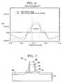
- FIG. 6is a graph of the results of a numerical simulation of the stress, Sxx, in a transistor channel as a function of horizontal distance in microns along a device substrate for both before (solid line) and after (dashed line) removing a nitride cap in a region 5 nm below the gate oxide for a polysilicon gate 60 nm wide, where the nitride film has a stress, Sxx, of 2.0 GPa formed in the transistor channel which is greater than approximately 4.5 ⁇ 10 9 dynes/cm 2 at about 5 nm below a gate oxide, and a 50 nm thick spacer, which may be one implementing feature of the invention.
- the enhanced stress in the transistor channelis greater than approximately 5.5 ⁇ 10 9 dynes/cm 2 at about 5 nm below a gate oxide.
- the numerical simulationshows that stress in the corresponding transistor channel increases 39% when the Si 3 N 4 Stack is removed from the top region of the gate, especially when the Si 3 N 4 is removed from gate sidewalls near the top of the gate stack.
- FIG. 7illustrates a semiconductor device having a silicon substrate 12 with a gate oxide 14 thereon.
- the silicon substrate 12has salicide region 24 .
- a polysilicon gate 16 with gate sidewalls 18is located on the gate oxide 14 .
- a gate salicide region 26is formed on top of the polysilicon gate 16 .
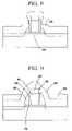
- a Si 3 N 4 spacer 36is added to the device shown in FIG. 7 .
- the spacer 36 of FIG. 7occupies a small region on the surface of the silicon substrate 12 and gate sidewalls 18 , as well as being formed on the lower region of the gate stack. That is, the spacer is not provided along the entire sidewall.
- Such a configurationminimizes the amount of Si 3 N 4 formed near the top of the gate stack.
- the Si 3 N 4 spacer 36may be formed by various processes, such as, for example, recessing the Si 3 N 4 4 spacer 36 using RIE process, which is selective to SiO 2 and silicide. Any other process which may form a Si 3 N 4 spacer towards the bottom of the gate stack may be used, as can be implemented by those of skill in the art.
- a non-conformal Si 3 N 4 or nitride layer 38is deposited on the device using, for example, a PECVD process so that there is little or no Si 3 N 4 deposited on the gate sidewalls 18 .
- the nitride structureterminates more abruptly creating stress concentrators or raisers, which enhance the stress formed in a transistor channel 40 .
- any processsuch as, for example, high density plasma deposition, which may deposit a non-conformal nitride film may be used.
- any processwhich preferentially reduces the amount of nitride deposited on the gate sidewalls 18 may be used.
- a spin-on material 42such as, for example, ARC (antireflection coating), oxide, or SILKTM (a combination of silicon and low k dielectric material) is applied.
- the materialis preferentially deposited in the low spots and leaves the high spots uncoated.
- any material which may act as a resist when the nitride film 28 is subsequently removedmay be a suitable spin-on material.
- the spin-on coating methodleaves the high points of the nitride film 28 exposed for further processing.
- Other methods which preferentially deposit material in the low regions and leave the high region exposedmay used to form film on top of the nitride film 28 .
- the exposed portion of the nitride film 28is removed through a Si 3 N 4 RIE process so that the nitride film 28 is preferentially removed only from the top of the gate stack.
- the upper portion of the gate stackis released from the nitride film 28 while the top of the silicon substrate remains covered.
- Such selective removal of the nitride film 28forms a transistor channel 44 having enhanced stress therein due to the silicon substrate 12 remaining covered.
- the nitride film 28may be removed by any process which preferentially removes the nitride film 28 and leaves the spin-on material 42 .
- FIGS. 11-13illustrate another embodiment by which a transistor channel having enhanced stress may be formed.
- a semiconductor device like that shown in FIG. 9is illustrated having a silicon substrate 12 with a gate oxide 14 thereon.
- the silicon substrate 12has salicide regions 24 .
- a polysilicon gate 16 with gate sidewalls 18is located on the gate oxide 14 .
- a gate salicide region 26is formed on top of the polysilicon gate 16 , all of which is known by those of skill in the art and implemented in accordance with known practices.
- a nitride coating 28 with exposed high spots and spin-on material 42is shown.
- an oxide layer(HDP (high density plasma) oxide or BPSG (borophosphorosilicate glass) may be applied leaving the high spots of the nitride film 28 exposed.
- HDPhigh density plasma
- BPSGborophosphorosilicate glass
- any material which may act as a resist when the nitride film 28 is subsequently removedmay be a suitable spin-on material.
- the waferis planarized using CMP to remove the exposed portion of the nitride film 28 and the top region of the gate stack. Accordingly, the silicon substrate 12 remains covered with nitride film 28 while the top of the gate stack is removed. By removing the top of the gate stack along with any nitride film 28 formed thereon, an enhanced stress transistor channel 46 is formed within the silicon substrate 12 . Any other known method to planarize the wafer may be used to remove the top of the gate stack.
- the spin-on material 42is removed, and a salicide gate region 48 is formed on the top of the gate stack. Any method which preferentially removes the spin-on material may used for this step.
- the resulting structureincludes a substrate covered with a nitride film, while avoiding nitride film on an upper portion of a gate stack. It should be noted that the method illustrated in FIGS. 11-13 may be readily applicable to a replacement gate process.
Landscapes
- Insulated Gate Type Field-Effect Transistor (AREA)
Abstract
Description
Claims (15)
Priority Applications (1)
| Application Number | Priority Date | Filing Date | Title |
|---|---|---|---|
| US11/467,446US7462915B2 (en) | 2004-01-16 | 2006-08-25 | Method and apparatus for increase strain effect in a transistor channel |
Applications Claiming Priority (2)
| Application Number | Priority Date | Filing Date | Title |
|---|---|---|---|
| US10/707,842US7118999B2 (en) | 2004-01-16 | 2004-01-16 | Method and apparatus to increase strain effect in a transistor channel |
| US11/467,446US7462915B2 (en) | 2004-01-16 | 2006-08-25 | Method and apparatus for increase strain effect in a transistor channel |
Related Parent Applications (1)
| Application Number | Title | Priority Date | Filing Date |
|---|---|---|---|
| US10/707,842DivisionUS7118999B2 (en) | 2004-01-16 | 2004-01-16 | Method and apparatus to increase strain effect in a transistor channel |
Publications (2)
| Publication Number | Publication Date |
|---|---|
| US20060286786A1 US20060286786A1 (en) | 2006-12-21 |
| US7462915B2true US7462915B2 (en) | 2008-12-09 |
Family
ID=34749150
Family Applications (3)
| Application Number | Title | Priority Date | Filing Date |
|---|---|---|---|
| US10/707,842Expired - LifetimeUS7118999B2 (en) | 2004-01-16 | 2004-01-16 | Method and apparatus to increase strain effect in a transistor channel |
| US11/465,663Expired - LifetimeUS7790558B2 (en) | 2004-01-16 | 2006-08-18 | Method and apparatus for increase strain effect in a transistor channel |
| US11/467,446Expired - LifetimeUS7462915B2 (en) | 2004-01-16 | 2006-08-25 | Method and apparatus for increase strain effect in a transistor channel |
Family Applications Before (2)
| Application Number | Title | Priority Date | Filing Date |
|---|---|---|---|
| US10/707,842Expired - LifetimeUS7118999B2 (en) | 2004-01-16 | 2004-01-16 | Method and apparatus to increase strain effect in a transistor channel |
| US11/465,663Expired - LifetimeUS7790558B2 (en) | 2004-01-16 | 2006-08-18 | Method and apparatus for increase strain effect in a transistor channel |
Country Status (3)
| Country | Link |
|---|---|
| US (3) | US7118999B2 (en) |
| CN (1) | CN100385635C (en) |
| TW (1) | TWI377596B (en) |
Cited By (4)
| Publication number | Priority date | Publication date | Assignee | Title |
|---|---|---|---|---|
| US20080128823A1 (en)* | 2006-11-30 | 2008-06-05 | Shinji Takeoka | Semiconductor device and method for fabricating the same |
| US20110101469A1 (en)* | 2009-10-30 | 2011-05-05 | Stephan Kronholz | Strain enhancement in transistors comprising an embedded strain-inducing semiconductor alloy by corner rounding at the top of the gate electrode |
| US20150087126A1 (en)* | 2012-10-01 | 2015-03-26 | United Microelectronics Corp. | Method of fabrication transistor with non-uniform stress layer with stress concentrated regions |
| US20160163798A1 (en)* | 2010-10-07 | 2016-06-09 | Sangjine Park | Semiconductor devices and methods for manufacturing the same |
Families Citing this family (22)
| Publication number | Priority date | Publication date | Assignee | Title |
|---|---|---|---|---|
| US7118999B2 (en)* | 2004-01-16 | 2006-10-10 | International Business Machines Corporation | Method and apparatus to increase strain effect in a transistor channel |
| US7361973B2 (en) | 2004-05-21 | 2008-04-22 | International Business Machines Corporation | Embedded stressed nitride liners for CMOS performance improvement |
| EP1717864A1 (en)* | 2005-04-27 | 2006-11-02 | STMicroelectronics ( Crolles 2) SAS | Method for managing the stress configuration in the channel of a MOS transistor, and corresponding integrated circuit. |
| US7262484B2 (en)* | 2005-05-09 | 2007-08-28 | International Business Machines Corporation | Structure and method for performance improvement in vertical bipolar transistors |
| US20070013070A1 (en)* | 2005-06-23 | 2007-01-18 | Liang Mong S | Semiconductor devices and methods of manufacture thereof |
| US7615432B2 (en)* | 2005-11-02 | 2009-11-10 | Samsung Electronics Co., Ltd. | HDP/PECVD methods of fabricating stress nitride structures for field effect transistors |
| US8729635B2 (en)* | 2006-01-18 | 2014-05-20 | Macronix International Co., Ltd. | Semiconductor device having a high stress material layer |
| US7410875B2 (en)* | 2006-04-06 | 2008-08-12 | United Microelectronics Corp. | Semiconductor structure and fabrication thereof |
| US7361539B2 (en)* | 2006-05-16 | 2008-04-22 | International Business Machines Corporation | Dual stress liner |
| US7514370B2 (en)* | 2006-05-19 | 2009-04-07 | International Business Machines Corporation | Compressive nitride film and method of manufacturing thereof |
| US20070275530A1 (en)* | 2006-05-24 | 2007-11-29 | Wen-Han Hung | Semiconductor structure and fabricating method thereof |
| US7768041B2 (en)* | 2006-06-21 | 2010-08-03 | International Business Machines Corporation | Multiple conduction state devices having differently stressed liners |
| WO2008027471A1 (en)* | 2006-08-31 | 2008-03-06 | Advanced Micro Devices, Inc. | A field effect transistor having a stressed contact etch stop layer with reduced conformality |
| DE102006040762B4 (en)* | 2006-08-31 | 2009-05-07 | Advanced Micro Devices, Inc., Sunnyvale | N-channel field effect transistor with a contact etch stop layer in conjunction with an interlayer dielectric sublayer having the same type of internal stress |
| DE102006040765B4 (en)* | 2006-08-31 | 2011-02-03 | Advanced Micro Devices, Inc., Sunnyvale | A method of fabricating a field effect transistor having a strained low-conformance contact etch stop layer and field effect transistor |
| US7935588B2 (en)* | 2007-03-06 | 2011-05-03 | International Business Machines Corporation | Enhanced transistor performance by non-conformal stressed layers |
| KR20090008568A (en)* | 2007-07-18 | 2009-01-22 | 주식회사 동부하이텍 | Manufacturing method of semiconductor device |
| US7820518B2 (en)* | 2008-05-29 | 2010-10-26 | Infineon Technologies Ag | Transistor fabrication methods and structures thereof |
| ES2828721T3 (en)* | 2008-10-14 | 2021-05-27 | Genentech Inc | Immunoglobulin variants and their uses |
| CN102299154B (en)* | 2010-06-22 | 2013-06-12 | 中国科学院微电子研究所 | Semiconductor structure and manufacturing method thereof |
| US8448124B2 (en) | 2011-09-20 | 2013-05-21 | International Business Machines Corporation | Post timing layout modification for performance |
| AU2013288641B2 (en) | 2012-07-13 | 2017-07-06 | Roche Glycart Ag | Bispecific anti-VEGF/anti-ANG-2 antibodies and their use in the treatment of ocular vascular diseases |
Citations (92)
| Publication number | Priority date | Publication date | Assignee | Title |
|---|---|---|---|---|
| US3602841A (en) | 1970-06-18 | 1971-08-31 | Ibm | High frequency bulk semiconductor amplifiers and oscillators |
| US4665415A (en) | 1985-04-24 | 1987-05-12 | International Business Machines Corporation | Semiconductor device with hole conduction via strained lattice |
| JPS6476755A (en) | 1987-09-18 | 1989-03-22 | Hitachi Ltd | Semiconductor device |
| US4853076A (en) | 1983-12-29 | 1989-08-01 | Massachusetts Institute Of Technology | Semiconductor thin films |
| US4855245A (en) | 1985-09-13 | 1989-08-08 | Siemens Aktiengesellschaft | Method of manufacturing integrated circuit containing bipolar and complementary MOS transistors on a common substrate |
| US4952524A (en) | 1989-05-05 | 1990-08-28 | At&T Bell Laboratories | Semiconductor device manufacture including trench formation |
| US4958213A (en) | 1987-12-07 | 1990-09-18 | Texas Instruments Incorporated | Method for forming a transistor base region under thick oxide |
| US5006913A (en) | 1988-11-05 | 1991-04-09 | Mitsubishi Denki Kabushiki Kaisha | Stacked type semiconductor device |
| US5060030A (en) | 1990-07-18 | 1991-10-22 | Raytheon Company | Pseudomorphic HEMT having strained compensation layer |
| US5081513A (en) | 1991-02-28 | 1992-01-14 | Xerox Corporation | Electronic device with recovery layer proximate to active layer |
| US5108843A (en) | 1988-11-30 | 1992-04-28 | Ricoh Company, Ltd. | Thin film semiconductor and process for producing the same |
| US5134085A (en) | 1991-11-21 | 1992-07-28 | Micron Technology, Inc. | Reduced-mask, split-polysilicon CMOS process, incorporating stacked-capacitor cells, for fabricating multi-megabit dynamic random access memories |
| US5310446A (en) | 1990-01-10 | 1994-05-10 | Ricoh Company, Ltd. | Method for producing semiconductor film |
| US5354695A (en) | 1992-04-08 | 1994-10-11 | Leedy Glenn J | Membrane dielectric isolation IC fabrication |
| US5371399A (en) | 1991-06-14 | 1994-12-06 | International Business Machines Corporation | Compound semiconductor having metallic inclusions and devices fabricated therefrom |
| US5391510A (en) | 1992-02-28 | 1995-02-21 | International Business Machines Corporation | Formation of self-aligned metal gate FETs using a benignant removable gate material during high temperature steps |
| US5459346A (en) | 1988-06-28 | 1995-10-17 | Ricoh Co., Ltd. | Semiconductor substrate with electrical contact in groove |
| US5557122A (en) | 1995-05-12 | 1996-09-17 | Alliance Semiconductors Corporation | Semiconductor electrode having improved grain structure and oxide growth properties |
| US5561302A (en) | 1994-09-26 | 1996-10-01 | Motorola, Inc. | Enhanced mobility MOSFET device and method |
| US5670798A (en) | 1995-03-29 | 1997-09-23 | North Carolina State University | Integrated heterostructures of Group III-V nitride semiconductor materials including epitaxial ohmic contact non-nitride buffer layer and methods of fabricating same |
| US5679965A (en) | 1995-03-29 | 1997-10-21 | North Carolina State University | Integrated heterostructures of Group III-V nitride semiconductor materials including epitaxial ohmic contact, non-nitride buffer layer and methods of fabricating same |
| US5861651A (en) | 1997-02-28 | 1999-01-19 | Lucent Technologies Inc. | Field effect devices and capacitors with improved thin film dielectrics and method for making same |
| US5880040A (en) | 1996-04-15 | 1999-03-09 | Macronix International Co., Ltd. | Gate dielectric based on oxynitride grown in N2 O and annealed in NO |
| US5940736A (en) | 1997-03-11 | 1999-08-17 | Lucent Technologies Inc. | Method for forming a high quality ultrathin gate oxide layer |
| US5960297A (en) | 1997-07-02 | 1999-09-28 | Kabushiki Kaisha Toshiba | Shallow trench isolation structure and method of forming the same |
| US5989978A (en) | 1998-07-16 | 1999-11-23 | Chartered Semiconductor Manufacturing, Ltd. | Shallow trench isolation of MOSFETS with reduced corner parasitic currents |
| US6008126A (en) | 1992-04-08 | 1999-12-28 | Elm Technology Corporation | Membrane dielectric isolation IC fabrication |
| US6025280A (en) | 1997-04-28 | 2000-02-15 | Lucent Technologies Inc. | Use of SiD4 for deposition of ultra thin and controllable oxides |
| US6066545A (en) | 1997-12-09 | 2000-05-23 | Texas Instruments Incorporated | Birdsbeak encroachment using combination of wet and dry etch for isolation nitride |
| US6090684A (en) | 1998-07-31 | 2000-07-18 | Hitachi, Ltd. | Method for manufacturing semiconductor device |
| US6107143A (en) | 1998-03-02 | 2000-08-22 | Samsung Electronics Co., Ltd. | Method for forming a trench isolation structure in an integrated circuit |
| US6117722A (en) | 1999-02-18 | 2000-09-12 | Taiwan Semiconductor Manufacturing Company | SRAM layout for relaxing mechanical stress in shallow trench isolation technology and method of manufacture thereof |
| US6133071A (en) | 1997-10-15 | 2000-10-17 | Nec Corporation | Semiconductor device with plate heat sink free from cracks due to thermal stress and process for assembling it with package |
| US6153501A (en) | 1998-05-19 | 2000-11-28 | Micron Technology, Inc. | Method of reducing overetch during the formation of a semiconductor device |
| US6165383A (en) | 1998-04-10 | 2000-12-26 | Organic Display Technology | Useful precursors for organic electroluminescent materials and devices made from such materials |
| US6198144B1 (en) | 1999-08-18 | 2001-03-06 | Micron Technology, Inc. | Passivation of sidewalls of a word line stack |
| US6221735B1 (en) | 2000-02-15 | 2001-04-24 | Philips Semiconductors, Inc. | Method for eliminating stress induced dislocations in CMOS devices |
| US6228694B1 (en) | 1999-06-28 | 2001-05-08 | Intel Corporation | Method of increasing the mobility of MOS transistors by use of localized stress regions |
| US6255169B1 (en) | 1999-02-22 | 2001-07-03 | Advanced Micro Devices, Inc. | Process for fabricating a high-endurance non-volatile memory device |
| US6261964B1 (en) | 1997-03-14 | 2001-07-17 | Micron Technology, Inc. | Material removal method for forming a structure |
| US6265317B1 (en) | 2001-01-09 | 2001-07-24 | Taiwan Semiconductor Manufacturing Company | Top corner rounding for shallow trench isolation |
| US20010009784A1 (en) | 1998-01-09 | 2001-07-26 | Yanjun Ma | Structure and method of making a sub-micron MOS transistor |
| US6274444B1 (en) | 1999-07-30 | 2001-08-14 | United Microelectronics Corp. | Method for forming mosfet |
| US6277720B1 (en)* | 1997-06-30 | 2001-08-21 | Texas Instruments Incorporated | Silicon nitride dopant diffusion barrier in integrated circuits |
| US6281532B1 (en) | 1999-06-28 | 2001-08-28 | Intel Corporation | Technique to obtain increased channel mobilities in NMOS transistors by gate electrode engineering |
| US6284623B1 (en) | 1999-10-25 | 2001-09-04 | Peng-Fei Zhang | Method of fabricating semiconductor devices using shallow trench isolation with reduced narrow channel effect |
| US6284626B1 (en) | 1999-04-06 | 2001-09-04 | Vantis Corporation | Angled nitrogen ion implantation for minimizing mechanical stress on side walls of an isolation trench |
| US6319794B1 (en) | 1998-10-14 | 2001-11-20 | International Business Machines Corporation | Structure and method for producing low leakage isolation devices |
| US6362082B1 (en) | 1999-06-28 | 2002-03-26 | Intel Corporation | Methodology for control of short channel effects in MOS transistors |
| US6361885B1 (en) | 1998-04-10 | 2002-03-26 | Organic Display Technology | Organic electroluminescent materials and device made from such materials |
| US6368931B1 (en) | 2000-03-27 | 2002-04-09 | Intel Corporation | Thin tensile layers in shallow trench isolation and method of making same |
| US20020063292A1 (en) | 2000-11-29 | 2002-05-30 | Mark Armstrong | CMOS fabrication process utilizing special transistor orientation |
| US6403975B1 (en) | 1996-04-09 | 2002-06-11 | Max-Planck Gesellschaft Zur Forderung Der Wissenschafteneev | Semiconductor components, in particular photodetectors, light emitting diodes, optical modulators and waveguides with multilayer structures grown on silicon substrates |
| US6403486B1 (en) | 2001-04-30 | 2002-06-11 | Taiwan Semiconductor Manufacturing Company | Method for forming a shallow trench isolation |
| US6406973B1 (en) | 1999-06-29 | 2002-06-18 | Hyundai Electronics Industries Co., Ltd. | Transistor in a semiconductor device and method of manufacturing the same |
| US20020086497A1 (en) | 2000-12-30 | 2002-07-04 | Kwok Siang Ping | Beaker shape trench with nitride pull-back for STI |
| US20020086472A1 (en) | 2000-12-29 | 2002-07-04 | Brian Roberds | Technique to obtain high mobility channels in MOS transistors by forming a strain layer on an underside of a channel |
| US20020090791A1 (en) | 1999-06-28 | 2002-07-11 | Brian S. Doyle | Method for reduced capacitance interconnect system using gaseous implants into the ild |
| US20020115288A1 (en)* | 2001-02-21 | 2002-08-22 | Bing-Chang Wu | Method for decreasing the resistivity of the gate and the leaky junction of the source/drain |
| US6461936B1 (en) | 2002-01-04 | 2002-10-08 | Infineon Technologies Ag | Double pullback method of filling an isolation trench |
| US6476462B2 (en) | 1999-12-28 | 2002-11-05 | Texas Instruments Incorporated | MOS-type semiconductor device and method for making same |
| US6483171B1 (en) | 1999-08-13 | 2002-11-19 | Micron Technology, Inc. | Vertical sub-micron CMOS transistors on (110), (111), (311), (511), and higher order surfaces of bulk, SOI and thin film structures and method of forming same |
| US6493497B1 (en) | 2000-09-26 | 2002-12-10 | Motorola, Inc. | Electro-optic structure and process for fabricating same |
| US6498358B1 (en) | 2001-07-20 | 2002-12-24 | Motorola, Inc. | Structure and method for fabricating an electro-optic system having an electrochromic diffraction grating |
| US6501121B1 (en) | 2000-11-15 | 2002-12-31 | Motorola, Inc. | Semiconductor structure |
| US6506652B2 (en) | 1998-11-13 | 2003-01-14 | Intel Corporation | Method of recessing spacers to improved salicide resistance on polysilicon gates |
| US20030032261A1 (en) | 2001-08-08 | 2003-02-13 | Ling-Yen Yeh | Method of preventing threshold voltage of MOS transistor from being decreased by shallow trench isolation formation |
| US20030040158A1 (en) | 2001-08-21 | 2003-02-27 | Nec Corporation | Semiconductor device and method of fabricating the same |
| US6531369B1 (en) | 2000-03-01 | 2003-03-11 | Applied Micro Circuits Corporation | Heterojunction bipolar transistor (HBT) fabrication using a selectively deposited silicon germanium (SiGe) |
| US6531740B2 (en) | 2001-07-17 | 2003-03-11 | Motorola, Inc. | Integrated impedance matching and stability network |
| US20030057184A1 (en) | 2001-09-22 | 2003-03-27 | Shiuh-Sheng Yu | Method for pull back SiN to increase rounding effect in a shallow trench isolation process |
| US20030067035A1 (en) | 2001-09-28 | 2003-04-10 | Helmut Tews | Gate processing method with reduced gate oxide corner and edge thinning |
| US6717216B1 (en) | 2002-12-12 | 2004-04-06 | International Business Machines Corporation | SOI based field effect transistor having a compressive film in undercut area under the channel and a method of making the device |
| US6825529B2 (en) | 2002-12-12 | 2004-11-30 | International Business Machines Corporation | Stress inducing spacers |
| US20040238914A1 (en) | 2003-05-30 | 2004-12-02 | International Business Machines Corporation | STI stress modification by nitrogen plasma treatment for improving performance in small width devices |
| US6831292B2 (en) | 2001-09-21 | 2004-12-14 | Amberwave Systems Corporation | Semiconductor structures employing strained material layers with defined impurity gradients and methods for fabricating same |
| US20040262784A1 (en) | 2003-06-30 | 2004-12-30 | International Business Machines Corporation | High performance cmos device structures and method of manufacture |
| US20050082634A1 (en) | 2003-10-16 | 2005-04-21 | International Business Machines Corporation | High performance strained cmos devices |
| US20050093030A1 (en) | 2003-10-30 | 2005-05-05 | Doris Bruce B. | Structure and method to enhance both nFET and pFET performance using different kinds of stressed layers |
| US20050098829A1 (en) | 2003-11-06 | 2005-05-12 | Doris Bruce B. | High mobility CMOS circuits |
| US20050106799A1 (en) | 2003-11-14 | 2005-05-19 | International Business Machines Corporation | Stressed semiconductor device structures having granular semiconductor material |
| US20050136583A1 (en)* | 2003-12-23 | 2005-06-23 | Taiwan Semiconductor Manufacturing Co. | Advanced strained-channel technique to improve CMOS performance |
| US20050145954A1 (en) | 2004-01-05 | 2005-07-07 | International Business Machines Corporation | Structures and methods for making strained mosfets |
| US20050194699A1 (en) | 2004-03-03 | 2005-09-08 | International Business Machines Corporation | Mobility enhanced cmos devices |
| US20050236668A1 (en) | 2004-04-23 | 2005-10-27 | International Business Machines Corporation | STRUCTURES AND METHODS FOR MANUFACTURING OF DISLOCATION FREE STRESSED CHANNELS IN BULK SILICON AND SOI CMOS DEVICES BY GATE STRESS ENGINEERING WITH SiGe AND/OR Si:C |
| US20050245017A1 (en) | 2003-10-30 | 2005-11-03 | Belyansky Michael P | Structure and method to improve channel mobility by gate electrode stress modification |
| US6974981B2 (en) | 2002-12-12 | 2005-12-13 | International Business Machines Corporation | Isolation structures for imposing stress patterns |
| US20060057787A1 (en) | 2002-11-25 | 2006-03-16 | Doris Bruce B | Strained finfet cmos device structures |
| US20060060925A1 (en) | 2004-09-17 | 2006-03-23 | International Business Machines Corporation | Semiconductor device structure with active regions having different surface directions and methods |
| US20060281272A1 (en)* | 2004-01-16 | 2006-12-14 | International Business Machines Corporation | Method and apparatus for increase strain effect in a transistor channel |
| US20070158752A1 (en)* | 2006-01-10 | 2007-07-12 | Anderson Brent A | Sram array and analog fet with dual-strain layers |
| US20080122003A1 (en)* | 2006-11-03 | 2008-05-29 | International Business Machines Corporation | Non-conformal stress liner for enhanced mosfet performance |
Family Cites Families (4)
| Publication number | Priority date | Publication date | Assignee | Title |
|---|---|---|---|---|
| US5264395A (en)* | 1992-12-16 | 1993-11-23 | International Business Machines Corporation | Thin SOI layer for fully depleted field effect transistors |
| US6521540B1 (en)* | 1999-07-01 | 2003-02-18 | Chartered Semiconductor Manufacturing Ltd. | Method for making self-aligned contacts to source/drain without a hard mask layer |
| JP2002198368A (en)* | 2000-12-26 | 2002-07-12 | Nec Corp | Method for manufacturing semiconductor device |
| US6586289B1 (en)* | 2001-06-15 | 2003-07-01 | International Business Machines Corporation | Anti-spacer structure for improved gate activation |
- 2004
- 2004-01-16USUS10/707,842patent/US7118999B2/ennot_activeExpired - Lifetime
- 2005
- 2005-01-03TWTW094100066Apatent/TWI377596B/ennot_activeIP Right Cessation
- 2005-01-14CNCNB2005100043050Apatent/CN100385635C/ennot_activeExpired - Lifetime
- 2006
- 2006-08-18USUS11/465,663patent/US7790558B2/ennot_activeExpired - Lifetime
- 2006-08-25USUS11/467,446patent/US7462915B2/ennot_activeExpired - Lifetime
Patent Citations (112)
| Publication number | Priority date | Publication date | Assignee | Title |
|---|---|---|---|---|
| US3602841A (en) | 1970-06-18 | 1971-08-31 | Ibm | High frequency bulk semiconductor amplifiers and oscillators |
| US4853076A (en) | 1983-12-29 | 1989-08-01 | Massachusetts Institute Of Technology | Semiconductor thin films |
| US4665415A (en) | 1985-04-24 | 1987-05-12 | International Business Machines Corporation | Semiconductor device with hole conduction via strained lattice |
| US4855245A (en) | 1985-09-13 | 1989-08-08 | Siemens Aktiengesellschaft | Method of manufacturing integrated circuit containing bipolar and complementary MOS transistors on a common substrate |
| JPS6476755A (en) | 1987-09-18 | 1989-03-22 | Hitachi Ltd | Semiconductor device |
| US4958213A (en) | 1987-12-07 | 1990-09-18 | Texas Instruments Incorporated | Method for forming a transistor base region under thick oxide |
| US5565697A (en) | 1988-06-28 | 1996-10-15 | Ricoh Company, Ltd. | Semiconductor structure having island forming grooves |
| US5459346A (en) | 1988-06-28 | 1995-10-17 | Ricoh Co., Ltd. | Semiconductor substrate with electrical contact in groove |
| US5006913A (en) | 1988-11-05 | 1991-04-09 | Mitsubishi Denki Kabushiki Kaisha | Stacked type semiconductor device |
| US5108843A (en) | 1988-11-30 | 1992-04-28 | Ricoh Company, Ltd. | Thin film semiconductor and process for producing the same |
| US4952524A (en) | 1989-05-05 | 1990-08-28 | At&T Bell Laboratories | Semiconductor device manufacture including trench formation |
| US5310446A (en) | 1990-01-10 | 1994-05-10 | Ricoh Company, Ltd. | Method for producing semiconductor film |
| US5060030A (en) | 1990-07-18 | 1991-10-22 | Raytheon Company | Pseudomorphic HEMT having strained compensation layer |
| US5081513A (en) | 1991-02-28 | 1992-01-14 | Xerox Corporation | Electronic device with recovery layer proximate to active layer |
| US5371399A (en) | 1991-06-14 | 1994-12-06 | International Business Machines Corporation | Compound semiconductor having metallic inclusions and devices fabricated therefrom |
| US5471948A (en) | 1991-06-14 | 1995-12-05 | International Business Machines Corporation | Method of making a compound semiconductor having metallic inclusions |
| US5134085A (en) | 1991-11-21 | 1992-07-28 | Micron Technology, Inc. | Reduced-mask, split-polysilicon CMOS process, incorporating stacked-capacitor cells, for fabricating multi-megabit dynamic random access memories |
| US5391510A (en) | 1992-02-28 | 1995-02-21 | International Business Machines Corporation | Formation of self-aligned metal gate FETs using a benignant removable gate material during high temperature steps |
| US6008126A (en) | 1992-04-08 | 1999-12-28 | Elm Technology Corporation | Membrane dielectric isolation IC fabrication |
| US5946559A (en) | 1992-04-08 | 1999-08-31 | Elm Technology Corporation | Membrane dielectric isolation IC fabrication |
| US5354695A (en) | 1992-04-08 | 1994-10-11 | Leedy Glenn J | Membrane dielectric isolation IC fabrication |
| US5571741A (en) | 1992-04-08 | 1996-11-05 | Leedy; Glenn J. | Membrane dielectric isolation IC fabrication |
| US5592018A (en) | 1992-04-08 | 1997-01-07 | Leedy; Glenn J. | Membrane dielectric isolation IC fabrication |
| US5592007A (en) | 1992-04-08 | 1997-01-07 | Leedy; Glenn J. | Membrane dielectric isolation transistor fabrication |
| US5840593A (en) | 1992-04-08 | 1998-11-24 | Elm Technology Corporation | Membrane dielectric isolation IC fabrication |
| US5683934A (en) | 1994-09-26 | 1997-11-04 | Motorola, Inc. | Enhanced mobility MOSFET device and method |
| US5561302A (en) | 1994-09-26 | 1996-10-01 | Motorola, Inc. | Enhanced mobility MOSFET device and method |
| US6046464A (en) | 1995-03-29 | 2000-04-04 | North Carolina State University | Integrated heterostructures of group III-V nitride semiconductor materials including epitaxial ohmic contact comprising multiple quantum well |
| US5670798A (en) | 1995-03-29 | 1997-09-23 | North Carolina State University | Integrated heterostructures of Group III-V nitride semiconductor materials including epitaxial ohmic contact non-nitride buffer layer and methods of fabricating same |
| US5679965A (en) | 1995-03-29 | 1997-10-21 | North Carolina State University | Integrated heterostructures of Group III-V nitride semiconductor materials including epitaxial ohmic contact, non-nitride buffer layer and methods of fabricating same |
| US5557122A (en) | 1995-05-12 | 1996-09-17 | Alliance Semiconductors Corporation | Semiconductor electrode having improved grain structure and oxide growth properties |
| US6403975B1 (en) | 1996-04-09 | 2002-06-11 | Max-Planck Gesellschaft Zur Forderung Der Wissenschafteneev | Semiconductor components, in particular photodetectors, light emitting diodes, optical modulators and waveguides with multilayer structures grown on silicon substrates |
| US5880040A (en) | 1996-04-15 | 1999-03-09 | Macronix International Co., Ltd. | Gate dielectric based on oxynitride grown in N2 O and annealed in NO |
| US5861651A (en) | 1997-02-28 | 1999-01-19 | Lucent Technologies Inc. | Field effect devices and capacitors with improved thin film dielectrics and method for making same |
| US5940736A (en) | 1997-03-11 | 1999-08-17 | Lucent Technologies Inc. | Method for forming a high quality ultrathin gate oxide layer |
| US6246095B1 (en) | 1997-03-11 | 2001-06-12 | Agere Systems Guardian Corp. | System and method for forming a uniform thin gate oxide layer |
| US6261964B1 (en) | 1997-03-14 | 2001-07-17 | Micron Technology, Inc. | Material removal method for forming a structure |
| US6025280A (en) | 1997-04-28 | 2000-02-15 | Lucent Technologies Inc. | Use of SiD4 for deposition of ultra thin and controllable oxides |
| US6277720B1 (en)* | 1997-06-30 | 2001-08-21 | Texas Instruments Incorporated | Silicon nitride dopant diffusion barrier in integrated circuits |
| US5960297A (en) | 1997-07-02 | 1999-09-28 | Kabushiki Kaisha Toshiba | Shallow trench isolation structure and method of forming the same |
| US6133071A (en) | 1997-10-15 | 2000-10-17 | Nec Corporation | Semiconductor device with plate heat sink free from cracks due to thermal stress and process for assembling it with package |
| US6066545A (en) | 1997-12-09 | 2000-05-23 | Texas Instruments Incorporated | Birdsbeak encroachment using combination of wet and dry etch for isolation nitride |
| US20010009784A1 (en) | 1998-01-09 | 2001-07-26 | Yanjun Ma | Structure and method of making a sub-micron MOS transistor |
| US6107143A (en) | 1998-03-02 | 2000-08-22 | Samsung Electronics Co., Ltd. | Method for forming a trench isolation structure in an integrated circuit |
| US6361885B1 (en) | 1998-04-10 | 2002-03-26 | Organic Display Technology | Organic electroluminescent materials and device made from such materials |
| US6165383A (en) | 1998-04-10 | 2000-12-26 | Organic Display Technology | Useful precursors for organic electroluminescent materials and devices made from such materials |
| US6153501A (en) | 1998-05-19 | 2000-11-28 | Micron Technology, Inc. | Method of reducing overetch during the formation of a semiconductor device |
| US5989978A (en) | 1998-07-16 | 1999-11-23 | Chartered Semiconductor Manufacturing, Ltd. | Shallow trench isolation of MOSFETS with reduced corner parasitic currents |
| US6090684A (en) | 1998-07-31 | 2000-07-18 | Hitachi, Ltd. | Method for manufacturing semiconductor device |
| US6319794B1 (en) | 1998-10-14 | 2001-11-20 | International Business Machines Corporation | Structure and method for producing low leakage isolation devices |
| US6506652B2 (en) | 1998-11-13 | 2003-01-14 | Intel Corporation | Method of recessing spacers to improved salicide resistance on polysilicon gates |
| US6509618B2 (en) | 1998-11-13 | 2003-01-21 | Intel Corporation | Device having thin first spacers and partially recessed thick second spacers for improved salicide resistance on polysilicon gates |
| US6521964B1 (en) | 1998-11-13 | 2003-02-18 | Intel Corporation | Device having spacers for improved salicide resistance on polysilicon gates |
| US6117722A (en) | 1999-02-18 | 2000-09-12 | Taiwan Semiconductor Manufacturing Company | SRAM layout for relaxing mechanical stress in shallow trench isolation technology and method of manufacture thereof |
| US6255169B1 (en) | 1999-02-22 | 2001-07-03 | Advanced Micro Devices, Inc. | Process for fabricating a high-endurance non-volatile memory device |
| US6284626B1 (en) | 1999-04-06 | 2001-09-04 | Vantis Corporation | Angled nitrogen ion implantation for minimizing mechanical stress on side walls of an isolation trench |
| US6228694B1 (en) | 1999-06-28 | 2001-05-08 | Intel Corporation | Method of increasing the mobility of MOS transistors by use of localized stress regions |
| US6281532B1 (en) | 1999-06-28 | 2001-08-28 | Intel Corporation | Technique to obtain increased channel mobilities in NMOS transistors by gate electrode engineering |
| US6362082B1 (en) | 1999-06-28 | 2002-03-26 | Intel Corporation | Methodology for control of short channel effects in MOS transistors |
| US20020090791A1 (en) | 1999-06-28 | 2002-07-11 | Brian S. Doyle | Method for reduced capacitance interconnect system using gaseous implants into the ild |
| US20020074598A1 (en) | 1999-06-28 | 2002-06-20 | Doyle Brian S. | Methodology for control of short channel effects in MOS transistors |
| US6406973B1 (en) | 1999-06-29 | 2002-06-18 | Hyundai Electronics Industries Co., Ltd. | Transistor in a semiconductor device and method of manufacturing the same |
| US6274444B1 (en) | 1999-07-30 | 2001-08-14 | United Microelectronics Corp. | Method for forming mosfet |
| US6483171B1 (en) | 1999-08-13 | 2002-11-19 | Micron Technology, Inc. | Vertical sub-micron CMOS transistors on (110), (111), (311), (511), and higher order surfaces of bulk, SOI and thin film structures and method of forming same |
| US6198144B1 (en) | 1999-08-18 | 2001-03-06 | Micron Technology, Inc. | Passivation of sidewalls of a word line stack |
| US6284623B1 (en) | 1999-10-25 | 2001-09-04 | Peng-Fei Zhang | Method of fabricating semiconductor devices using shallow trench isolation with reduced narrow channel effect |
| US6476462B2 (en) | 1999-12-28 | 2002-11-05 | Texas Instruments Incorporated | MOS-type semiconductor device and method for making same |
| US6221735B1 (en) | 2000-02-15 | 2001-04-24 | Philips Semiconductors, Inc. | Method for eliminating stress induced dislocations in CMOS devices |
| US6531369B1 (en) | 2000-03-01 | 2003-03-11 | Applied Micro Circuits Corporation | Heterojunction bipolar transistor (HBT) fabrication using a selectively deposited silicon germanium (SiGe) |
| US6368931B1 (en) | 2000-03-27 | 2002-04-09 | Intel Corporation | Thin tensile layers in shallow trench isolation and method of making same |
| US6493497B1 (en) | 2000-09-26 | 2002-12-10 | Motorola, Inc. | Electro-optic structure and process for fabricating same |
| US6501121B1 (en) | 2000-11-15 | 2002-12-31 | Motorola, Inc. | Semiconductor structure |
| US20020063292A1 (en) | 2000-11-29 | 2002-05-30 | Mark Armstrong | CMOS fabrication process utilizing special transistor orientation |
| US20020086472A1 (en) | 2000-12-29 | 2002-07-04 | Brian Roberds | Technique to obtain high mobility channels in MOS transistors by forming a strain layer on an underside of a channel |
| US20020086497A1 (en) | 2000-12-30 | 2002-07-04 | Kwok Siang Ping | Beaker shape trench with nitride pull-back for STI |
| US6265317B1 (en) | 2001-01-09 | 2001-07-24 | Taiwan Semiconductor Manufacturing Company | Top corner rounding for shallow trench isolation |
| US20020115288A1 (en)* | 2001-02-21 | 2002-08-22 | Bing-Chang Wu | Method for decreasing the resistivity of the gate and the leaky junction of the source/drain |
| US6403486B1 (en) | 2001-04-30 | 2002-06-11 | Taiwan Semiconductor Manufacturing Company | Method for forming a shallow trench isolation |
| US6531740B2 (en) | 2001-07-17 | 2003-03-11 | Motorola, Inc. | Integrated impedance matching and stability network |
| US6498358B1 (en) | 2001-07-20 | 2002-12-24 | Motorola, Inc. | Structure and method for fabricating an electro-optic system having an electrochromic diffraction grating |
| US20030032261A1 (en) | 2001-08-08 | 2003-02-13 | Ling-Yen Yeh | Method of preventing threshold voltage of MOS transistor from being decreased by shallow trench isolation formation |
| US20030040158A1 (en) | 2001-08-21 | 2003-02-27 | Nec Corporation | Semiconductor device and method of fabricating the same |
| US6831292B2 (en) | 2001-09-21 | 2004-12-14 | Amberwave Systems Corporation | Semiconductor structures employing strained material layers with defined impurity gradients and methods for fabricating same |
| US20030057184A1 (en) | 2001-09-22 | 2003-03-27 | Shiuh-Sheng Yu | Method for pull back SiN to increase rounding effect in a shallow trench isolation process |
| US20030067035A1 (en) | 2001-09-28 | 2003-04-10 | Helmut Tews | Gate processing method with reduced gate oxide corner and edge thinning |
| US6461936B1 (en) | 2002-01-04 | 2002-10-08 | Infineon Technologies Ag | Double pullback method of filling an isolation trench |
| US20060057787A1 (en) | 2002-11-25 | 2006-03-16 | Doris Bruce B | Strained finfet cmos device structures |
| US6974981B2 (en) | 2002-12-12 | 2005-12-13 | International Business Machines Corporation | Isolation structures for imposing stress patterns |
| US6825529B2 (en) | 2002-12-12 | 2004-11-30 | International Business Machines Corporation | Stress inducing spacers |
| US20050040460A1 (en) | 2002-12-12 | 2005-02-24 | Dureseti Chidambarrao | Stress inducing spacers |
| US6717216B1 (en) | 2002-12-12 | 2004-04-06 | International Business Machines Corporation | SOI based field effect transistor having a compressive film in undercut area under the channel and a method of making the device |
| US20050280051A1 (en) | 2002-12-12 | 2005-12-22 | Dureseti Chidambarrao | Isolation structures for imposing stress patterns |
| US20040238914A1 (en) | 2003-05-30 | 2004-12-02 | International Business Machines Corporation | STI stress modification by nitrogen plasma treatment for improving performance in small width devices |
| US20040262784A1 (en) | 2003-06-30 | 2004-12-30 | International Business Machines Corporation | High performance cmos device structures and method of manufacture |
| US20050082634A1 (en) | 2003-10-16 | 2005-04-21 | International Business Machines Corporation | High performance strained cmos devices |
| US20050148146A1 (en) | 2003-10-16 | 2005-07-07 | Doris Bruce D. | High performance strained CMOS devices |
| US20050245017A1 (en) | 2003-10-30 | 2005-11-03 | Belyansky Michael P | Structure and method to improve channel mobility by gate electrode stress modification |
| US20050093030A1 (en) | 2003-10-30 | 2005-05-05 | Doris Bruce B. | Structure and method to enhance both nFET and pFET performance using different kinds of stressed layers |
| US20050282325A1 (en) | 2003-10-30 | 2005-12-22 | Belyansky Michael P | Structure and method to improve channel mobility by gate electrode stress modification |
| US6977194B2 (en) | 2003-10-30 | 2005-12-20 | International Business Machines Corporation | Structure and method to improve channel mobility by gate electrode stress modification |
| US7015082B2 (en) | 2003-11-06 | 2006-03-21 | International Business Machines Corporation | High mobility CMOS circuits |
| US20050098829A1 (en) | 2003-11-06 | 2005-05-12 | Doris Bruce B. | High mobility CMOS circuits |
| US20060027868A1 (en) | 2003-11-06 | 2006-02-09 | Ibm Corporation | High mobility CMOS circuits |
| US20050106799A1 (en) | 2003-11-14 | 2005-05-19 | International Business Machines Corporation | Stressed semiconductor device structures having granular semiconductor material |
| US20050136583A1 (en)* | 2003-12-23 | 2005-06-23 | Taiwan Semiconductor Manufacturing Co. | Advanced strained-channel technique to improve CMOS performance |
| US20050145954A1 (en) | 2004-01-05 | 2005-07-07 | International Business Machines Corporation | Structures and methods for making strained mosfets |
| US20060281272A1 (en)* | 2004-01-16 | 2006-12-14 | International Business Machines Corporation | Method and apparatus for increase strain effect in a transistor channel |
| US20050194699A1 (en) | 2004-03-03 | 2005-09-08 | International Business Machines Corporation | Mobility enhanced cmos devices |
| US20050236668A1 (en) | 2004-04-23 | 2005-10-27 | International Business Machines Corporation | STRUCTURES AND METHODS FOR MANUFACTURING OF DISLOCATION FREE STRESSED CHANNELS IN BULK SILICON AND SOI CMOS DEVICES BY GATE STRESS ENGINEERING WITH SiGe AND/OR Si:C |
| US20060060925A1 (en) | 2004-09-17 | 2006-03-23 | International Business Machines Corporation | Semiconductor device structure with active regions having different surface directions and methods |
| US20070158752A1 (en)* | 2006-01-10 | 2007-07-12 | Anderson Brent A | Sram array and analog fet with dual-strain layers |
| US20080122003A1 (en)* | 2006-11-03 | 2008-05-29 | International Business Machines Corporation | Non-conformal stress liner for enhanced mosfet performance |
Non-Patent Citations (22)
| Title |
|---|
| A. Shimizu, et al., "Mechanical-Stress Effect of Etch-Stop Nitride and its Impact on Deep Submicron Transistor Design," International Electron Devices Meeting, IEEE, Mar. 2001. |
| B. Doyle, et al., "Recovery of Hot-Carrier Damage in Reoxidized Nitrided Oxide MOSFETs." IEEE Electron Device Letters, vol. 13, No. 1, Jan. 1992, pp. 38-40. |
| C.J. Huang, et al., "Temperature Dependence and Post-Stress Recovery of Hot Electron Degradation Effects in Bipolar Transistors." IEEE 1991, Bipolar Circuits and Technology Meeting 7.5, pp. 170-173. |
| D.C. Houghton, et al., "Equilibrium Critical Thickness for SI 1-x GEx Strained Layers on (100) Si". Appl. Phys. Lett. 56 (5), Jan. 29, 1990, pp. 460-462. |
| F. Ootsuka, et a., "A Highly Dense, High-Performance 130nm node CMOS Technology for Large Scale System-on-a-Chip Application," International Electron Devices Meeting, 23.5.1, IEEE, Apr. 2000. |
| G. Zhang, et al., "A New 'Mixed-Mode' Reliability Degradation Mechanism in Advanced Si and SiGe Bipolar Transistors." IEEE Transactions on Electron Devices, vol. 49, No. 12, Dec. 2002, pp. 2151-2156. |
| Gregory Scott, et al., "NMOS drive Current Reduction Caused by Transistor Layout and Trench Isolation Induced Stress," International Electron Devices Meeting, 33.4.1, IEEE, Sep. 1999. |
| H. Li, et al., "Design of W-Band VCOs with High Output Power for Potential Application in 77 GHz Automotive Radar Systems." 2003, IEEE GaAs Digest, pp. 263-266. |
| H. Wurzer, et al., "Annealing of Degraded non-Transistors-Mechanisms and Modeling." IEEE Transactions on Electron Devices, vol. 41, No. 4, Apr. 1994, pp. 533-538. |
| H.S. Momose, et al. "Analysis of the Temperature Dependence of Hot-Carrier-Induced Degradation in Bipolar Transistors for Bi-CMOS." IEEE Transactions on Electron Devices, vol. 41, No. 6, Jun. 1994, pp. 978-987. |
| H.S. Momose, et al., "Temperature Dependence of Emitter-Base Reverse Stress Degradation and its Mechanism Analyzed by MOS Structures." 1989 IEEE, Paper 6.2, pp. 140-143. |
| J.C. Bean, et al., "GEx SI 1-x/Si Strained-Layer Superlattice Grown by Molecular Beam Epitaxy", J. Vac. Sci. Technol. A 2(2), Apr.-Jun. 1984, pp. 436-440. |
| J.H. Van Der Merwe, "Regular Articles". Journal of Applied Physics, vol. 34, No. 1, Jan. 1963, pp. 117-122. |
| J.W. Matthews, et al., "Defects in Epitaxial Multilayers". Journal of Crystal Growth 27 (1974), pp. 118-125. |
| K. Ota, et al., "Novel Locally Strained Channel Technique for High Performance 55nm CMOS," International Electron Devices Meeting, 2.2.1, IEEE, Feb. 2002. |
| Kem Rim, et al., "Characteristics and Device Design of Sub-100 nm Straing Si N- and PMOSFETS," 2002 Symposium On VLSI Technology Digest of Technical Papers, IEEE, pp. 98-99. |
| Kem Rim, et al., "Transconductance Enhancement in Deep Submicron Strained-Si n-MOSFETS," International Electron Devices Meeting, 26, 8, 1, IEEE, Sep. 1998. |
| M. Khater, et al., "SiGe HBT Technology with Fmax/Ft=350/300 GHz and Gate Delay Below 3.3 ps".2004 IEEE, 4 pages. |
| Q. Quyang et al., "Two-Dimensional Bandgap Engineering in a Novel Si/SiGe pMOSFET with Enhanced Device Performance and Scalability". 2000, IEEE, pp. 151-154. |
| R.H.M. Van De Leur, et al., "Critical Thickness for Pseudomorphic Growth of Si/Ge Alloys and Superlattices". J. Appl. Phys. 64 (6), Sep. 15, 1988, pp. 3043-3050. |
| Shinya Ito, et al., "Mechanical Stress Effect of Etch-Stop Nitride and its Impact on Deep Submicron Transistor Design," International Electron Devices Meeting, 23.5.1, IEEE, Apr. 2000. |
| Subramanian S. Iyer, et al. "Heterojuction Bipolar Transistors Using Si-Ge Alloys". IEEE Transactions on Electron Devices, vol. 36, No. 10, Oct. 1989, pp. 2043-2064. |
Cited By (8)
| Publication number | Priority date | Publication date | Assignee | Title |
|---|---|---|---|---|
| US20080128823A1 (en)* | 2006-11-30 | 2008-06-05 | Shinji Takeoka | Semiconductor device and method for fabricating the same |
| US7781844B2 (en)* | 2006-11-30 | 2010-08-24 | Panasonic Corporation | Semiconductor device having a stressor film |
| US20110101469A1 (en)* | 2009-10-30 | 2011-05-05 | Stephan Kronholz | Strain enhancement in transistors comprising an embedded strain-inducing semiconductor alloy by corner rounding at the top of the gate electrode |
| US8338892B2 (en)* | 2009-10-30 | 2012-12-25 | Globalfoundries Inc. | Strain enhancement in transistors comprising an embedded strain-inducing semiconductor alloy by corner rounding at the top of the gate electrode |
| US20160163798A1 (en)* | 2010-10-07 | 2016-06-09 | Sangjine Park | Semiconductor devices and methods for manufacturing the same |
| US10128336B2 (en)* | 2010-10-07 | 2018-11-13 | Samsung Electronics Co., Ltd. | Semiconductor devices and methods for manufacturing the same |
| US20150087126A1 (en)* | 2012-10-01 | 2015-03-26 | United Microelectronics Corp. | Method of fabrication transistor with non-uniform stress layer with stress concentrated regions |
| US9343573B2 (en)* | 2012-10-01 | 2016-05-17 | United Microelectronics Corp. | Method of fabrication transistor with non-uniform stress layer with stress concentrated regions |
Also Published As
| Publication number | Publication date |
|---|---|
| CN100385635C (en) | 2008-04-30 |
| US7118999B2 (en) | 2006-10-10 |
| TWI377596B (en) | 2012-11-21 |
| US20060286786A1 (en) | 2006-12-21 |
| CN1641848A (en) | 2005-07-20 |
| TW200534348A (en) | 2005-10-16 |
| US7790558B2 (en) | 2010-09-07 |
| US20060281272A1 (en) | 2006-12-14 |
| US20050158955A1 (en) | 2005-07-21 |
Similar Documents
| Publication | Publication Date | Title |
|---|---|---|
| US7462915B2 (en) | Method and apparatus for increase strain effect in a transistor channel | |
| US7465620B2 (en) | Transistor mobility improvement by adjusting stress in shallow trench isolation | |
| US7759206B2 (en) | Methods of forming semiconductor devices using embedded L-shape spacers | |
| US6882025B2 (en) | Strained-channel transistor and methods of manufacture | |
| CN100428497C (en) | Fabrication structure and method of strained semiconductor CMOS transistor | |
| US8324038B2 (en) | Method of removing a spacer, method of manufacturing a metal-oxide-semiconductor transistor device, and metal-oxide-semiconductor transistor device | |
| US7164189B2 (en) | Slim spacer device and manufacturing method | |
| US5858867A (en) | Method of making an inverse-T tungsten gate | |
| US8253177B2 (en) | Strained channel transistor | |
| US7777284B2 (en) | Metal-oxide-semiconductor transistor and method of forming the same | |
| US20070108525A1 (en) | Structure and method to increase strain enhancement with spacerless fet and dual liner process | |
| US20060189053A1 (en) | PMOS transistor with discontinuous CESL and method of fabrication | |
| US7612389B2 (en) | Embedded SiGe stressor with tensile strain for NMOS current enhancement | |
| JP2006517343A (en) | MOSFET device having tensile strained substrate and method of making the same | |
| CN1783496A (en) | Structure and method of applying stresses to PFET and NFET transistor channels for improved performance | |
| US20100078687A1 (en) | Method for Transistor Fabrication with Optimized Performance | |
| US20090065807A1 (en) | Semiconductor device and fabrication method for the same | |
| US7253481B2 (en) | High performance MOS device with graded silicide | |
| KR101071787B1 (en) | Semiconductor structure with enhanced performance using a simplified dual stress liner configuration | |
| CN1979786B (en) | method for manufacturing strained silicon transistor | |
| US7081392B2 (en) | Method for fabricating a gate structure of a FET and gate structure of a FET | |
| JP3020729B2 (en) | Method for manufacturing semiconductor device | |
| US20040198058A1 (en) | Methods of forming field effect transistor gates |
Legal Events
| Date | Code | Title | Description |
|---|---|---|---|
| FEPP | Fee payment procedure | Free format text:PAYOR NUMBER ASSIGNED (ORIGINAL EVENT CODE: ASPN); ENTITY STATUS OF PATENT OWNER: LARGE ENTITY | |
| STCF | Information on status: patent grant | Free format text:PATENTED CASE | |
| REMI | Maintenance fee reminder mailed | ||
| FPAY | Fee payment | Year of fee payment:4 | |
| SULP | Surcharge for late payment | ||
| AS | Assignment | Owner name:GLOBALFOUNDRIES U.S. 2 LLC, NEW YORK Free format text:ASSIGNMENT OF ASSIGNORS INTEREST;ASSIGNOR:INTERNATIONAL BUSINESS MACHINES CORPORATION;REEL/FRAME:036550/0001 Effective date:20150629 | |
| AS | Assignment | Owner name:GLOBALFOUNDRIES INC., CAYMAN ISLANDS Free format text:ASSIGNMENT OF ASSIGNORS INTEREST;ASSIGNORS:GLOBALFOUNDRIES U.S. 2 LLC;GLOBALFOUNDRIES U.S. INC.;REEL/FRAME:036779/0001 Effective date:20150910 | |
| FPAY | Fee payment | Year of fee payment:8 | |
| AS | Assignment | Owner name:WILMINGTON TRUST, NATIONAL ASSOCIATION, DELAWARE Free format text:SECURITY AGREEMENT;ASSIGNOR:GLOBALFOUNDRIES INC.;REEL/FRAME:049490/0001 Effective date:20181127 | |
| MAFP | Maintenance fee payment | Free format text:PAYMENT OF MAINTENANCE FEE, 12TH YEAR, LARGE ENTITY (ORIGINAL EVENT CODE: M1553); ENTITY STATUS OF PATENT OWNER: LARGE ENTITY Year of fee payment:12 | |
| AS | Assignment | Owner name:GLOBALFOUNDRIES U.S. INC., CALIFORNIA Free format text:ASSIGNMENT OF ASSIGNORS INTEREST;ASSIGNOR:GLOBALFOUNDRIES INC.;REEL/FRAME:054633/0001 Effective date:20201022 | |
| AS | Assignment | Owner name:GLOBALFOUNDRIES INC., CAYMAN ISLANDS Free format text:RELEASE BY SECURED PARTY;ASSIGNOR:WILMINGTON TRUST, NATIONAL ASSOCIATION;REEL/FRAME:054636/0001 Effective date:20201117 | |
| AS | Assignment | Owner name:GLOBALFOUNDRIES U.S. INC., NEW YORK Free format text:RELEASE BY SECURED PARTY;ASSIGNOR:WILMINGTON TRUST, NATIONAL ASSOCIATION;REEL/FRAME:056987/0001 Effective date:20201117 |