US7462891B2 - Semiconductor device having an interconnect with sloped walls and method of forming the same - Google Patents
Semiconductor device having an interconnect with sloped walls and method of forming the sameDownload PDFInfo
- Publication number
- US7462891B2 US7462891B2US11/236,376US23637605AUS7462891B2US 7462891 B2US7462891 B2US 7462891B2US 23637605 AUS23637605 AUS 23637605AUS 7462891 B2US7462891 B2US 7462891B2
- Authority
- US
- United States
- Prior art keywords
- semiconductor device
- layer
- source
- recited
- formed over
- Prior art date
- Legal status (The legal status is an assumption and is not a legal conclusion. Google has not performed a legal analysis and makes no representation as to the accuracy of the status listed.)
- Expired - Fee Related
Links
Images


Classifications
- H—ELECTRICITY
- H10—SEMICONDUCTOR DEVICES; ELECTRIC SOLID-STATE DEVICES NOT OTHERWISE PROVIDED FOR
- H10D—INORGANIC ELECTRIC SEMICONDUCTOR DEVICES
- H10D64/00—Electrodes of devices having potential barriers
- H10D64/20—Electrodes characterised by their shapes, relative sizes or dispositions
- H10D64/23—Electrodes carrying the current to be rectified, amplified, oscillated or switched, e.g. sources, drains, anodes or cathodes
- H10D64/251—Source or drain electrodes for field-effect devices
- H10D64/256—Source or drain electrodes for field-effect devices for lateral devices wherein the source or drain electrodes are recessed in semiconductor bodies
- H—ELECTRICITY
- H01—ELECTRIC ELEMENTS
- H01L—SEMICONDUCTOR DEVICES NOT COVERED BY CLASS H10
- H01L21/00—Processes or apparatus adapted for the manufacture or treatment of semiconductor or solid state devices or of parts thereof
- H01L21/02—Manufacture or treatment of semiconductor devices or of parts thereof
- H01L21/04—Manufacture or treatment of semiconductor devices or of parts thereof the devices having potential barriers, e.g. a PN junction, depletion layer or carrier concentration layer
- H01L21/18—Manufacture or treatment of semiconductor devices or of parts thereof the devices having potential barriers, e.g. a PN junction, depletion layer or carrier concentration layer the devices having semiconductor bodies comprising elements of Group IV of the Periodic Table or AIIIBV compounds with or without impurities, e.g. doping materials
- H01L21/28—Manufacture of electrodes on semiconductor bodies using processes or apparatus not provided for in groups H01L21/20 - H01L21/268
- H01L21/283—Deposition of conductive or insulating materials for electrodes conducting electric current
- H01L21/285—Deposition of conductive or insulating materials for electrodes conducting electric current from a gas or vapour, e.g. condensation
- H01L21/28506—Deposition of conductive or insulating materials for electrodes conducting electric current from a gas or vapour, e.g. condensation of conductive layers
- H01L21/28575—Deposition of conductive or insulating materials for electrodes conducting electric current from a gas or vapour, e.g. condensation of conductive layers on semiconductor bodies comprising AIIIBV compounds
Definitions
- the present inventionis directed, in general, to semiconductor devices and, more specifically, to a semiconductor device having an interconnect with a sloped wall and a method of forming the same.
- a field-effect transistor(also referred to as a “FET”) is a conventional semiconductor device employable in switch-mode power supplies for use in data processing and telecommunication systems as well as for other applications that use conditioned power for the operation of sensitive electronic circuits.
- Field-effect transistorshave almost universally replaced bipolar transistors previously used for inverters (a type or portion of a power supply) as well as the p-n and Schottky diodes used for rectification.
- the proliferation of field-effect transistorshas, at least in part, been driven by the need to provide highly efficient power supplies with low dc output voltages such as five volts or less at higher current levels.
- field-effect transistorsfor the aforementioned applications is a consequence of the low forward voltage drop and fast switching speed as well as the low power consumption employed to enable or disable conduction thereof.
- the use of field-effect transistorshas contributed to compact and efficient power supplies that can be produced at low cost.
- a material of choice for high performance field-effect transistorsis a semiconductor with high electron mobility and wide band gap for high breakdown voltage that is capable of being processed with conventional equipment and methods not substantially different from those already developed for silicon and present generations of compound semiconductors.
- a particularly desirable materialis the compound semiconductor known as gallium arsenide (“GaAs”), which has been used for integrated circuits operable at frequencies well above one gigahertz, and which has been used to produce power field-effect transistors with high performance characteristics.
- GaAsgallium arsenide
- An exemplary performance of gallium arsenide in comparison to other semiconductor materials for high performance field-effect transistorsis described in “Fundamentals of III-V Devices” by W. Liu, published by John Wiley and Sons (1999), and “Modem GaAs Processing Methods” by R. Williams, published by Artech House (1990), which are incorporated herein by reference.
- gallium arsenide field-effect transistorsemploying a controllable vertical channel between a source and drain thereof are provided in the following references, namely, U.S. Pat. No. 5,889,298 entitled “Vertical JFET Field Effect Transistor,” by Plumton, et al., issued on Mar. 30, 1999, U.S. Pat. No. 5,342,795 entitled “Method of Fabricating Power VFET Gate-Refill,” by Yuan, et al., issued on Aug. 30, 1994, U.S. Pat. No. 5,468,661 entitled “Method of Making Power VFET Device,” by Yuan, et al., issued on Nov. 21, 1995, U.S. Pat. No.
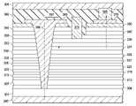
- the gallium arsenide field-effect transistorincludes buried and inter-coupled gate fingers (also referred to as a gate and one of which is designated 110 ) formed in etched trenches in an n-doped drain 120 thereby producing vertical channels 130 .
- the gates 110exhibit a gate length (generally designated “GL”) and the vertical channels 130 provide a channel opening (generally designated “CO”).
- the trenchesare back-filled epitaxially with p-doped gallium arsenide to form the gates 110 .
- a p+ implant 140provides a top surface contact to the gates 110 , and is made through a further n-doped epitaxial layer that forms a source 150 .
- External connection to the gates 110is made through metallized contacts 160 deposited over the heavily doped p+ implants 140 .
- An external source contact 170 and drain contact 180are made through metal depositions over further heavily doped areas.
- the structureproduces vertical field-effect transistor channels between the gates 110 , and provides source and drain contacts 170 , 180 , respectively, on opposing sides of The die. The device, therefore, operates with vertical carrier flow and the buried gates 110 , typically doped opposite from the vertical channels 130 , exhibit limited control over a fill profile thereof.
- the field-effect transistor as described abovedoes not accommodate a careful doping profiling and epitaxial layer design necessary to produce a modulation-doped channel that can be formed in a lateral channel and that may be employed to substantially reduce the on-resistance of the device.
- the field-effect transistor described aboveis not configured with a channel having a strained material, which would significantly improve a mobility of the current carrying carriers and, consequently, a switching speed thereof.
- This design methodology of constructing such gallium arsenide field-effect transistorshas been analyzed in the following references, namely, “Comparison of GaAs and Silicon Synchronous Rectifiers in a 3.3V Out, 50 W DC-DC Converter,” by V. A.
- the gallium arsenide field-effect transistor acting as a power field-effect transistorincludes a gate 205 interposed between a source 210 and drain 215 , creating a lateral channel in an n-doped GaAs layer 220 .
- a depletion region 225is formed under the gate 205 and a shallower depletion region 230 forms generally under an upper surface of the die as a result of an inherent existence of surface states at the surface of the crystal (i.e., a surface pinning effect).
- the gallium arsenide field-effect transistoris formed over a semi-insulating GaAs substrate 235 . Designing the source and drain contacts on the same surface of the die requires a complicated multilayer metallization process and results in increased die area and reduced chip yield. The aforementioned configuration can also lead to increased inductance, which is of significance in applications for microwave signal amplification. Also, the gallium arsenide field-effect transistor does not include an intrinsic body diode.
- the gallium arsenide field-effect transistorincludes a plated air bridge 250 coupled to a source (generally designated “S”) on an upper side of the die. Gates (generally designated “G”) are interposed between drains (generally designated “D”), and are also located on the upper surface of the die.
- Couplings to the sourceare brought down to a lower surface of the die by vias 265 that are plated-through holes between the lower surface and the source and are further coupled together by a plated heat sink 280 .
- this arrangementcan provide low-inductance external connections to the source, it is limited in its ability to provide a low-resistance channel tightly coupled to the lower surface of a highly conductive substrate, or an intrinsic body diode.
- the aforementioned designalso does not accommodate large drain contacts desirable for a higher power device, which will increase the resistive and inductive losses.
- This configurationrequires a complex air-bridge processing step, which will increase the cost and potentially affect the reliability of the device.
- the parasitic resistance in series with the sourcewill increase due to the long air-bridge connection.
- This designalso is incompatible with today's packaging techniques for higher power devices embodied in a vertical device configuration.
- U.S. Pat. No. 6,309,918 entitled “Manufacturable GaAs VFET Process,” by Huang, et al., issued on Oct. 30, 2001,is directed toward a vertical FET with source and drain contacts on opposing sides of a die.
- These devicesinclude an isolation trench surrounding the devices, etched to a lower semi-insulating gallium arsenide layer and backfilled with silicon nitride.
- the aforementioned devicesare configured with contacts on a top surface, which restricts their application from low voltage, high current systems wherein efficiency is an important design element.
- modulation dopingLow on-resistance compound semiconductor field-effect transistors have been enhanced by the use of a layering structure called modulation doping as described in “Fundamentals of III-V Devices” by W. Liu (pp. 323-330) and “Ultra-High Speed Modulation-Doped Field-Effect Transistors: A tutorial Review,” L. D. Nguyen, et al., Proceedings of the IEEE, Vol. 80, No. 4, pp. 494-518 (April 1992), which are incorporated herein by reference and are particularly applicable to devices with a lateral channel.
- the objective of modulation dopingis to avoid electron scattering in the current conducting channel by ionized impurities due to dopants, which increases channel resistivity due to the decreased carrier mobility.
- Channel conductivitymay be modulated by a separate control element such as a gate that controls channel depletion.
- the modulation doping techniquehas been developed for lateral channels using, for instance, gallium arsenide as an undoped, narrower band gap channel and including an adjacent, doped, wider band gap layer of aluminum gallium arsenide, which provides an abundant and controllable source of free carriers to the gallium arsenide channel.
- gallium arsenideas an undoped, narrower band gap channel and including an adjacent, doped, wider band gap layer of aluminum gallium arsenide, which provides an abundant and controllable source of free carriers to the gallium arsenide channel.
- Other combinations of compound semiconductorscan be used such as an undoped indium gallium arsenide channel and an adjacent, doped aluminum gallium arsenide layer as the source of free carriers.
- Successful and repeatable applications of modulation dopingwhich is based on precision formation of a pseudomorphic layer, employ lateral channel arrangements that are not presently available in devices configured with vertical channels.
- the need for devices with low resistance between a channel thereof, particularly a lateral channel, and a metallized contact area on a surface of the field-effect transistoris preferable.
- Current crowding effects at the junction between the channel and a conductive via, such as a source interconnect, coupling the channel to a metallic contact on the surface thereofalso adversely affect the resistance of the field-effect transistor.
- An additional problem for power field-effect transistors with a backside contact coupled through an interconnect to a channelis discontinuities in evaporated metal deposited in etched vias or trenches that couple the channel to the surface contact.
- the etched vias or trenchesare typically formed by anisotropic dry etching and have substantially right-angled edges that are produced by the etching process.
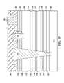
- an exemplary via or trench 292 in a semiconductor device 290is illustrated with sharp edges (generally designated 294 ) after anisotropic dry etching.
- the right-angled sharp edges 294are conducive to the formation of metallic discontinuities that can produce high resistance contacts and sometimes open circuits.
- a viais needed with substantial contact area to the semiconductor device, particularly to a channel thereof, and with sloped walls that can be metallized with ohmic metal stacks (e.g., gold-germanium-nickel) and alloyed after etching to produce a low resistance ohmic contact directly to the conducting horizontal channel (i.e., a low resistance interconnect).
- ohmic metal stackse.g., gold-germanium-nickel
- alloyed after etchingto produce a low resistance ohmic contact directly to the conducting horizontal channel (i.e., a low resistance interconnect).
- a current pathwill have significantly lower resistance than the conventional current path.
- a field-effect transistor exhibiting the aforementioned characteristicswould allow the development of more efficient and lower cost power supplies than are presently available.
- a field-effect transistor designis not presently available for the more severe applications that lie ahead. Accordingly, what is needed in the art is a gallium arsenide and other compound semiconductor devices with lower on-resistance configured for wide acceptance, particularly in low voltage and high current applications, overcoming many of the aforementioned limitations.
- a compact and efficient power supplyparticularly for very low voltage and high current loads such as microprocessors, as well as amplifiers for telecommunications and other applications, would benefit from a robust field-effect transistor without incurring unnecessary costs or the need to commit a substantial portion of the physical volume of the end device to the power supply.
- the semiconductor deviceincludes a conductive substrate having a first contact covering a substantial portion of a bottom surface thereof.
- the semiconductor devicealso includes a lateral channel above the conductive substrate.
- the semiconductor devicefurther includes a second contact above the lateral channel.
- the semiconductor devicestill further includes an interconnect having a sloped wall that connects the lateral channel to the conductive substrate. The interconnect is operable to provide a low resistance coupling between the first contact and the lateral channel.
- the first contactis a source contact and the second contact is a drain contact for the semiconductor device.
- the present inventionprovides a semiconductor device including a substrate having a source contact covering a substantial portion of a bottom surface thereof and a first buffer layer formed over the substrate. Additionally, the semiconductor device includes an isolation layer, a first spacer layer, a second buffer layer, a first barrier layer, and a second spacer layer formed between the first buffer layer and a first lateral channel. The semiconductor device also includes third and fourth spacer layers, a second lateral channel, fifth and sixth spacer layers and a third lateral channel formed over the first lateral channel. The semiconductor device also includes a seventh spacer layer and a second barrier layer formed over the third lateral channel. A recess layer and an etch-stop layer are thereafter formed between the second barrier layer and first and second source/drain contact layers.
- the semiconductor devicefurther includes a source interconnect having a sloped wall that connects the first, second and third lateral channels to the substrate operable to provide a low resistance coupling between the source contact and the first, second and third lateral channels.
- a gate of the semiconductor deviceis located in a gate recess formed though the first and second source/drain contact layers, the etch-stop and the recess layer.
- a dielectric layeris thereafter formed over the gate, and the first and second source/drain contact layers.
- the semiconductor devicestill further includes a drain post located in a drain via formed through the dielectric layer and over the first and second source/drain contact layers, and a drain contact coupled to the drain post.
- the present inventionprovides a semiconductor device including a conductive substrate having a first contact covering a substantial portion of a bottom surface thereof.
- the semiconductor devicealso includes a lateral channel above the conductive substrate, and a second contact above the lateral channel.
- the semiconductor devicefurther includes an interconnect having a sloped wall that connects the lateral channel to the conductive substrate operable to provide a low resistance coupling between the first contact and the lateral channel.
- the semiconductor devicestill further includes an intrinsic body diode operable to provide a conductive path between the first and second contacts.
- FIGS. 1 , 2 A, 2 B and 2 Cillustrate cross sectional views of field-effect transistors according to the prior art
- FIGS. 3 to 21illustrate cross sectional views of an embodiment of constructing a semiconductor device according to the principles of the present invention
- FIGS. 22 and 23illustrate cross sectional and perspective views, respectively, of another embodiment of a semiconductor device constructed according to the principles of the present invention
- FIG. 24illustrates a plan view of another embodiment of a semiconductor device constructed according to the principles of the present invention.
- FIG. 25illustrates an equivalent circuit diagram of a semiconductor device constructed according to the principles of the present invention.
- FIGS. 26 and 27illustrate plan views of another embodiment of a semiconductor device constructed according to the principles of the present invention.
- a substrate driven FETis configured with a source contact coupled to a substrate and a drain contact coupled to an opposing surface of the device to provide a low on-resistance switch with very fast switching transition times.
- the substrate driven FETalso includes at least one lateral channel to, among other things, further reduce an on-resistance thereof.
- the principles of the present inventionmay be applied to a compound semiconductor FET with modulation-doped lateral channel(s) and other semiconductor devices that include current-carrying channels including modulation-doped lateral channels and switched terminals on opposing surfaces thereof.
- an interconnecte.g., a source interconnect
- the substrate driven FETis formed with sloping walls to provide a low resistance ohmic contact between at least one lateral channel and a contact thereof (e.g., a source contact).
- the sloping walls of the source interconnectaccommodate vacuum deposition of a metallic layer thereon to facilitate formation of the low resistance ohmic contact.
- a Schottky diodemay also be coupled in parallel with the drain and source contacts of the substrate driven FET and formed on the same substrate.
- 2007/0045765entitled “Semiconductor Device Having Substrate-Driven Field-Effect Transistor and Schottky Diode and Method of Forming the Same,” to Brar, et al., published Mar. 1, 2007, which are incorporated herein by reference.
- the inclusion of multiple lateral channels in a semiconductor devicerecognizes the limited improvement in on-resistance that can be obtained by simply increasing the thickness of a single lateral channel.
- Carriers in the lateral channelflow near the channel edges due to highly localized electric field distributions within the lateral channel, and this limits an improvement of the on-resistance as the lateral channel is made thicker.
- a single thicker lateral channel made of material with a different lattice constant from a substrateexhibits more numerous atomic dislocations in the crystal lattice, which degrades the carrier mobility and device break down characteristics.
- a further benefit of multiple lateral channelsis an increase in transconductance of the semiconductor device for a given device area.
- Improvements in the on-resistance and transconductance for presently available semiconductor devicesordinarily come at the expense of greater die area, which has a direct effect on the cost and yield of the semiconductor device.
- the semiconductor devicecan achieve improvements in on-resistance and transconductance without the limitations as discussed above.
- the substrate driven FETmay be capable of switching transition times on the order of nanoseconds, rather than switching transition times on the order of 35 to 50 nanoseconds realizable with the present silicon-based technology.
- the substrate driven FETmay exhibit peak inverse voltage ratings such as 10 to 20 volts or less and should have low on-resistance including the parasitic electrical resistance from the device packaging approaching one milliohm or less.
- the substrate driven FETdesirably has gates that can be driven with digital logic, with low gate charge and correspondingly low and controllable field-effect transistor threshold voltage.
- the substrate driven FETalso desirably has current ratings of at least a dozen amperes, and should be cost competitive with presently available field-effect transistors having similar power ratings implemented in silicon-based technology.
- the substrate driven FETalso desirably includes an intrinsic body diode that is capable of conducting substantially the full rated device current.
- the substrate driven FET having source and drain contacts on opposing sides of the diefacilitates low resistance and inductance packaging by providing more area for the contacts.
- the substrate driven FETmay also operate as an enhancement-mode device which implies a normally-off device when a gate voltage is substantially zero volts to avoid short circuits during power supply start-up.
- the presence of an intrinsic body diode with the anode coupled to a source interconnect and source contactcan also provide substantial benefits in circuit design as well as cost reduction, particularly in power supply applications.
- the semiconductor deviceincludes a source interconnect with sloped walls to couple a lateral channel with a contact disposed on one surface of the substrate driven FET.
- the sloped walls of the source interconnectadvantageously provide a surface on which a metallic layer can be readily vacuum deposited to provide a low resistance ohmic coupling between the lateral channel and the source contact.
- the sloped wallsalso reduce internal electric fields in the semiconductor device to reduce current crowding, thereby further reducing on-resistance of the device.
- the resistance of the metallic layercan be reduced by increasing its thickness with a metal-plating process.
- the inclusion of a source interconnect with sloped walls and metallic platingcan be used to produce a low resistance semiconductor device such as a field-effect transistor that can be used to reduce the cost and increase the efficiency of, for instance, a power supply.
- boundariesmay be shown as lines to separate semiconductor regions or layers with apparent abrupt changes in doping levels or species. It is recognized that semiconductor manufacturing processes such as implantation and diffusion may cause doping concentrations and atomic species to vary in a continuous and sometimes gradual manner across a semiconductor device. Consequently, graded boundaries of device regions may be shown as lines in the drawings for explanatory purposes without compromising an understanding of the structure of the devices.
- GaAsgallium arsenide
- the basic stepsinclude, for example, molecular-beam epitaxy, metal-organic chemical vapor deposition, patterning, exposing, etching, vacuum depositing, plating, doping, alloying, annealing, and cleaning.
- Williamsdescribes many conventional processes for constructing a gallium arsenide device in “Modem GaAs Processing Methods.” Additionally, several separate processing steps may be generally combined into a single step within the scope of the present invention, such as a combined annealing step wherein a number of alloys that are separately deposited are heated together to jointly activate the alloys. Further, alternative methods to perform a processing step such as vacuum deposition, sputtering, or plating processes may be combined or performed separately without further elaboration herein. Also, while selected doping levels and characteristics such as thickness of layers that make up an exemplary substrate driven FET will hereinafter be provided, those skilled in the art understand that alternative doping levels and characteristics may be provided and still be within the broad scope of the present invention. For instance and in the appropriate circumstances, the layers may be oppositely doped, such as a p-type layer may be replaced with an n-type layer.
- the substrate driven FETis formed on a substrate (e.g., GaAs substrate) 301 .
- the substrate 301is n-doped and is a highly conductive layer (e.g., a conductive substrate) with a doping level in the range of 7 ⁇ 10 17 to 5 ⁇ 10 18 cm ⁇ 3 .
- the substrate 301may be chosen to be sufficiently thick to provide mechanical and chemical support for semiconductor processing and handling, and may be supported by a further underlying medium.
- the substrate 301provides a source connection for the substrate driven FET, accommodating a low-resistance connection over a substantial portion of the lower surface thereof.
- a preferred n-type doping material for GaAsis silicon (“Si”), but selenium (“Se”), tellurium (“Te”) or other doping materials or combinations thereof may be employed within the broad scope of the present invention.
- the substrate driven FET described hereinis GaAs based, alternative semiconductor materials may be employed to form the substrate 301 such as a semiconductor material based on indium-phosphide (“InP”) as well as oppositely doped semiconductors with essential properties of related materials appropriately altered.
- first buffer layere.g., an n+ epitaxial buffer layer
- n+ epitaxial buffer layere.g., an n+ epitaxial buffer layer
- a suitable n-type doping materialsuch as Si may be employed, but alternatively Se, Te or other n-type dopant or combinations thereof may be employed in the epitaxial growth process.
- a preferred doping densityis in the range of 7 ⁇ 10 17 to 5 ⁇ 10 18 cm ⁇ 3 .
- the addition of the first buffer layer 304generally provides a more uniform crystal structure for further epitaxial depositions than an ordinary, doped GaAs substrate 301 , and thus may be optionally included for the formation of the above layers for improved device characteristics.
- an isolation layere.g., a p-doped isolation layer
- a preferred thickness of the isolation layer 307is approximately 1000 ⁇ and a preferred dopant is carbon with a doping density between about 5 ⁇ 10 18 cm ⁇ 3 to 5 ⁇ 10 19 cm ⁇ 3 .
- a thickness of the isolation layer 307can range from about 300 ⁇ to 2000 ⁇ and beyond, and may be deposited with a doping density roughly inversely proportional to the thickness.
- the isolation layer 307forms a pair of back-to-back diodes with n-doped layers formed thereabove and the buffer layer 304 to substantially block current flow when the substrate driven FET is in a non-conducting state, particularly when a positive voltage is applied between the drain and source contacts thereof.
- the design parameters for the layers above the isolation layer 307elicit engineering trade-offs and should be chosen to preserve a lifetime of the minority carriers (i.e., electrons) injected therein so that the minority carriers diffuse through the substrate driven FET with sufficiently limited recombination.
- the above-referenced layersshould be designed to provide a high degree of conductivity for the substrate driven FET, limit a break-down, and limit the internal fields when the layer(s) above the isolation layer 307 act as the cathode for the back-to-back diodes, thereby providing reverse voltage blocking capability.
- the layers above the isolation layer 307 of the substrate driven FETshould be provided to enhance a performance thereof such as sustaining a high drain-to-source voltage (e.g., 20 volts) when the substrate driven FET is in a non-conducting state and to provide support for lateral channels formed thereover.
- a first spacer layer 313is a thick, but lightly doped p-type GaAs layer that is epitaxially deposited at about 10000 ⁇ and preferably lightly doped to about 1 ⁇ 10 15 cm ⁇ 3 above the isolation layer 307 .
- the first spacer layer 313limits an internal electric field within the substrate driven FET and helps to limit breakdown when the substrate driven FET is transitioned to a non-conducting state. As a result, an applied voltage is substantially blocked between the source and drain terminals thereof.
- the first spacer layer 313is lightly doped and sufficiently thick, such as 5000 ⁇ to 20000 ⁇ , to provide a sufficiently high voltage blocking capability for the substrate driven FET.
- Different layer thicknessranging from 5000 ⁇ to 20000 ⁇ and doping levels such as 1 ⁇ 10 15 cm ⁇ 3 to 5 ⁇ 10 16 cm ⁇ 3 may be used depending on, for example, the appropriate level of voltage blocking necessary for the substrate driven FET.
- An undoped layer or a lightly doped n-type layercan also be used in place of the lightly doped p-type layer.
- a second buffer layer 315 located above the first spacer layer 313is an alternating aluminum-gallium arsenide/gallium arsenide (“AlGaAs/GaAs”) super-lattice buffer that is sequentially deposited epitaxially to improve the smoothness of the surface of the crystal and to increase the mobility of the electrons in the channel to be formed thereabove.
- AlGaAs/GaAsaluminum-gallium arsenide/gallium arsenide
- the presence of aluminummay also act as a “getter” to capture and disable oxygen atoms that may otherwise be present in the subsequent growth.
- the second buffer layer 315is deposited preferably with ten alternating layers of AlGaAs (0.24 Al), preferably about 185 ⁇ thick, and GaAs, preferably about 15 ⁇ thick.
- the total thickness of the second buffer layer 315is approximately 2000 ⁇ .
- a first barrier layer 318 located above the second buffer layer 315is an aluminum-gallium arsenide-phosphide AlGaAsP (0.24 Al and 0.05 P) bottom barrier/spacer that is epitaxially deposited at approximately 1000 ⁇ to substantially block the free carriers from flowing down to the layers therebelow.
- An n-pulse doping with Si (“delta doped”), preferably to a level of about 4 ⁇ 10 12 cm ⁇ 2is thereafter performed thereon to supply the free carriers to the channel thereabove by the mechanism of modulation doping.
- the isolation layer 307therefore, lies between n-doped layers, thereby forming the back-to-back diodes that provide an isolation capability for the substrate driven FET.
- a cloud of free electrons positioned above the isolation layer 307is not able to substantially recombine therein.
- the effectis to enable a brief period of conduction in the parasitic n-p-n transistor wherein the n-doped layer above forms the emitter, the p-doped layers form the base, and the n-doped layer below forms the collector.
- the resulting parasitic transistoris able to shunt current between the source and the drain during transient conditions when, for instance, the substrate driven FET is transitioned to a non-conducting state.
- the parasitic transistortransitions to a non-conducting state.
- a second spacer layer 320e.g., a substantially undoped AlGaAsP (0.24 Al and 0.05 P) spacer
- a second spacer layer 320is then epitaxially deposited at approximately 40 ⁇ above the first barrier layer 318 to separate the effects of dopants from the channel, thereby separating the free carriers from the ionized sites and improving the electron mobility therein.
- a thin, indium-gallium arsenide (“InGaAs”) layerthat is epitaxially deposited with about 20% indium to form a first lateral channel 325 with controllable conductivity.
- the first lateral channel 325is inherently lattice-strained (i.e., it is “pseudomorphic”) and is preferably less than about 100 ⁇ to prevent lattice dislocations and formation of polycrystalline structures in the layers to be deposited thereabove.
- the lattice-strained channelprovides higher carrier mobility owing to a reduced effective mass of the carriers.
- the first lateral channel 325provides the controllable conduction mechanism between the source and drain of the substrate driven FET and provides a modulation-doped channel with reduced crystalline irregularities for the free carriers supplied by adjacent layers.
- a third spacer layer 326e.g., a substantially undoped AlGaAsP (0.24 Al and 0.05 P) spacer] is then epitaxially deposited at approximately 40 ⁇ above the first lateral channel 325 to separate the effects of dopants from the channel, thereby separating the free carriers from the ionized sites and improving the electron mobility therein.
- a fourth spacer layer 327e.g., a substantially undoped AlGaAsP (0.24 Al and 0.05 P) spacer] is then epitaxially deposited at approximately 40 ⁇ above the third spacer layer 326 to separate the effects of dopants from a second lateral channel to be deposited thereabove, again separating the free carriers from the ionized sites and improving the electron mobility of a second lateral channel.
- a substantially undoped AlGaAsP (0.24 Al and 0.05 P) spaceris then epitaxially deposited at approximately 40 ⁇ above the third spacer layer 326 to separate the effects of dopants from a second lateral channel to be deposited thereabove, again separating the free carriers from the ionized sites and improving the electron mobility of a second lateral channel.
- the fourth spacer layer 327is a second, thin, indium-gallium arsenide (“InGaAs”) layer that is epitaxially deposited with about 20% indium to form a second lateral channel 328 with controllable conductivity.
- the second lateral channel 328is inherently lattice-strained and is preferably less than about 100 ⁇ to prevent lattice dislocations and formation of polycrystalline structures in the layers to be deposited thereabove.
- a fifth spacer layer 329e.g., a substantially undoped AlGaAsP (0.24 Al and 0.05 P) spacer] is then epitaxially deposited at approximately 40 ⁇ above the second lateral channel 328 to separate the effects of dopants from the second lateral channel 328 as described hereinabove.
- An n-pulse doping with Si (“delta doped”), preferably to a level of about 4 ⁇ 10 12 cm ⁇ 2is thereafter performed thereon to supply the free carriers to the second lateral channel 328 and to a third lateral channel to be deposited thereabove by the mechanism of modulation doping.
- a sixth spacer layer 330e.g., a substantially undoped AlGaAsP (0.24 Al and 0.05 P) spacer] is then epitaxially deposited at approximately 40 ⁇ above the fifth spacer layer 329 to separate the effects of dopants from a third lateral channel above, thereby separating the free carriers from the ionized sites and improving the electron mobility of a third lateral channel.
- a substantially undoped AlGaAsP (0.24 Al and 0.05 P) spaceris then epitaxially deposited at approximately 40 ⁇ above the fifth spacer layer 329 to separate the effects of dopants from a third lateral channel above, thereby separating the free carriers from the ionized sites and improving the electron mobility of a third lateral channel.
- the sixth spacer layer 330is a third, thin, indium-gallium arsenide (“InGaAs”) layer that is epitaxially deposited with about 20% indium to form a third lateral channel 331 with controllable conductivity.
- the third lateral channel 331is inherently lattice-strained and is preferably less than about 100 ⁇ to reduce lattice dislocations and formation of polycrystalline structures in the layers to be deposited thereabove.
- the third lateral channel 331is another region that is epitaxially deposited including sub-layers of AlGaAsP (0.24 Al and 0.05 P) to provide additional free carriers (electrons) for modulation doping of the third lateral channel 331 , and to provide a barrier for the free carriers in the third lateral channel 331 .
- a seventh spacer layer 333is undoped and deposited at about 40 ⁇ to provide a spacer layer separating the free carriers in the third lateral channel 331 from ionized impurity sites.
- the inclusion of phosphorus in the spacer layers mentioned aboveprovides a mechanism to at least partially compensate for the mismatch of the lattice constant for the lateral channels.
- the lattice constant for InAsis 6.0584 ⁇ , which indicates that the inclusion of indium in the lateral channels increases the lattice constant thereof.
- the lattice constant for GaAswhich forms the foundation of the substrate driven FET, is 5.6533 ⁇ .
- the lattice constant for GaPis smaller (5.4512 ⁇ ) than that for GaAs and, as such, indicates that the inclusion of phosphorus in the spacer layers produces an opposite component of strain on the crystal thereby providing the compensation for the longer atomic spacing in the lateral channels resulting from the inclusion of indium atoms therein.
- the inclusion of phosphorusimproves carrier confinement in the lateral channels due to its wider bandgap as opposed to, for instance, AlGaAs with the same aluminum composition.
- the strain balancingcan be achieved by one of the following, namely, adjusting an indium composition in the lateral channels or a thickness thereof, and adjusting the phosphorous composition in the spacer layers or a thickness thereof.
- modulation dopingis preferably achieved by separating the channel-conduction carriers from the carrier-contributing donor atoms located in the Si-pulsed areas.
- the carrier mobility in the first, second and third lateral channels 325 , 328 , 331is thereby improved by providing a conductive path substantially undisturbed by lattice imperfections that would otherwise be affected by in-channel dopants.
- the semiconductor device as described hereinincludes three lateral channels, semiconductor devices with any number of lateral channels (e.g., one lateral channel) are well within the broad scope of the present invention.
- the concentration of phosphorous in the spacer layerswhich relaxes the strain from the indium as described above.
- the inclusion of a plurality of lateral channelsimproves the on-resistance of a semiconductor device designed with a given die area, almost in proportion to the number of lateral channels.
- the breakdown voltage of the semiconductor devicemay be increased by the inclusion of the multiple lateral channels due to the reduced localized electric distribution around the edges thereof.
- a second barrier layer 336(embodied in an undoped AlGaAs layer) is then epitaxially deposited at about 210 ⁇ with a doping level in the range of 1 ⁇ 10 17 to 5 ⁇ 10 17 cm ⁇ 3 or undoped.
- a recess layer 339 of GaAsis then epitaxially deposited, preferably at about 230 ⁇ and Si-doped with a doping level in the range of 1 ⁇ 10 17 to 5 ⁇ 10 17 or undoped.
- an etch-stop layer 340embodied in a thin aluminum-arsenide (“AlAs”), indium-phosphide (“InP”), or indium-gallium-phosphide (“InGaP”) epitaxial deposition is formed above the recess layer 339 .
- AlAsaluminum-arsenide
- InPindium-phosphide
- InGaPindium-gallium-phosphide
- the etch-stop layer 340provides an etch stop for a later, trench-forming process for GaAs layers to be further deposited and doped thereabove.
- the etch-stop layer 340is preferably about 25 ⁇ thick and can be doped n-type with a doping level in the range of 1 ⁇ 10 17 to 5 ⁇ 10 18 cm ⁇ 3 or undoped.
- layers of GaAsare epitaxially deposited above the etch-stop layer 340 to form source and drain contact layers for the substrate driven FET.
- a first source/drain contact layer 345 of about 300 ⁇ of an n-doped layer of GaAsis epitaxially deposited, preferably using Si as the dopant with a doping level in the range of 1 ⁇ 10 17 to 1 ⁇ 10 18 cm ⁇ 3 .
- a second source/drain contact layer 350 of about 500 ⁇ of a heavily doped n+ layer of GaAsis epitaxially deposited with a doping level in the range of 1 ⁇ 10 18 to 1 ⁇ 10 19 cm ⁇ 3 to improve formation of ohmic contacts for the source and drain and to reduce resistance in the source-to-gate and drain-to-gate regions of the channels.
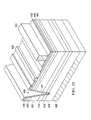
- FIGS. 11 to 15illustrated are cross sectional views of an embodiment of constructing a source interconnect through the substrate driven FET in accordance with the principles of the present invention.
- the source interconnectis configured to create a low-resistance ohmic contact between the first, second and third lateral channels (also referred to as “lateral channels”) 325 , 328 , 331 and the substrate 301 .
- the source interconnectis formed with sloped walls (e.g., sidewalls) to facilitate vacuum deposition of a metallic layer thereon.
- a spun-on positive photoresist 355is illustrated with respect to FIG. 11 that has been masked, exposed and developed as is well known in the art to form a trench for access to the layers therebelow. After a photolithography process (i.e., exposure to ultraviolet light and development of the exposed area), the photoresist pattern has substantially vertical walls.
- the photoresist 355is then baked (e.g., reflowed) such as on a hot plate or oven at about 110 to 150 degrees Celsius and in a normal atmosphere, which cures the photoresist 355 and causes a lower surface of the photoresist 355 facing the trench to encroach toward the trench, forming a generally angular aspect to the trench as illustrated with respect to FIG. 12 .
- the angle of the slope in the photoresist 355can be controlled by modifying a duration and temperature profile of the reflow process as is well understood in the art.
- the portion of the substrate driven FET unprotected by the photoresist 355is anisotropically dry etched, preferably using an inductively coupled plasma (i.e., an “ICP” dry etch).
- the anisotropic dry etchforms a source via (or trench) through the layers of the substrate driven FET down to the substrate 301 to create a low-resistance contact between the first, second and third lateral channels 325 , 328 , 331 and the substrate 301 .
- the non-selective etchingmay further alter a profile of the photoresist 355 .
- Gallium arsenideis generally etched faster than the photoresist 355 by the ICP dry etching, producing a general slope in the walls (generally designated 357 ) of the trench in exposed portions of the GaAs and can also produce sloping walls in exposed intervening layers (some slopes not shown).
- the etching processis preferably continued for a controlled period of time until the source via is opened to the substrate 301 .
- a thin etch-stop layersuch as heavily n-doped aluminum oxide or indium-gallium phosphide (“InGaP”) layer, both being substantially lattice-matched to the GaAs substrate, can be epitaxially deposited above the substrate 301 to form a barrier to limit the depth of the ICP dry etch.
- the etch-stop layershould not substantially affect conductivity to the substrate 301 , if it is sufficiently thin and doped and can be subsequently removed.
- an aluminum arsenide etch-stop layerwould be about 50-100 ⁇ thick depending on the proscribed etch resistance, but an InGaP layer which has better conductivity could be thicker.
- other processesmay be employed to form the source via with sloped walls (e.g., side walls) such as, without limitation, variations in baking temperature and baking time, and different dry etching methods including, but not limited to, reactive ion etching, inductively coupled plasma etching, and electron cyclotron resonance etching. As one skilled in the art will recognize, each variation will provide a different shape of the etching profile, which will affect the performance of the substrate driven FET.
- the walls 357 of the source viashould be sufficiently sloped so that a thin metal layer (generally designated 360 ) can be deposited on horizontal and semi-horizontal surfaces, preferably by a vacuum evaporation and deposition process.
- the metal materialis anisotropically deposited onto the horizontal surfaces such as the bottom of the source via and on the sloped surfaces.
- Augold
- germaniumGe
- Ninickel
- germaniummigrates at the elevated annealing temperature into the semiconductor material, forming an n + -doped region adjacent to the metal layer 360 , the heavily doped n + region enabling an ohmic contact between the metal layer 360 and other layers of the substrate driven FET.
- a low-resistance ohmic contactis also formed with the first buffer layer 304 located above the substrate 301 .
- Other alloyssuch as palladium-germanium-gold, nickel-indium-germanium, palladium-germanium and aluminum-tin-nickel may be employed to advantage. Annealing causes an alloy to form among the metallic species and allows migration of metal into adjacent semiconductor material forming a metal semiconductor eutectic, thereby enhancing its low-resistance, ohmic property.
- an electroplating processis thereafter performed to form a low-resistance source interconnect 365 .
- the source interconnect 365is filled with plated platinum and gold.
- the waferis dipped into a plating solution and is connected to an electrical current source.
- a metal material of the plating solutione.g., either platinum or gold
- the creation of the source interconnect 365enhances a metallic path between the highly conductive portions of the first, second and third lateral channels 325 , 328 , 331 and the substrate 301 .
- lateral channels 325 , 328 , 331 between a source contact and a drain contactcan be formed and a low-resistance contact to the source (coupled to the lateral channels 325 , 328 , 331 ) can be configured on an opposing surface of the substrate driven FET from a contact for the drain (also coupled to the lateral channels 325 , 328 , 331 ).
- an implantmay be formed to create the source interconnect such as illustrated in U.S. Patent Application Publication No. 2006/0226477, entitled “Substrate Driven Field-Effect Transistor,” to Brar, et al., published Oct. 12. 2006, which is incorporated herein by reference.
- a temperature profile of one to five minutes on a hot plate and 10 to 30 minutes in an ovenmay be used when curing the photoresist.
- etching a trench (or via) with sloped wallscan be achieved.
- a photoresist thickness of two micrometersmay be used with a photoresist pattern opening of one micrometer, and a baking temperature of 140 degrees Celsius for a baking time of three minutes, reducing an angle of the wall of the photoresist from substantially 90 degrees to about 37 degrees and the angle of the wall of the via from substantially 90 degrees to about 73 degrees. Due to the thickness change of the photoresist on the substrate driven FET from the reflow process, the etching profile thereof under the photoresist will be shaped by the profile of the reflowed photoresist. Since the etch rate of substrate driven FET is typically higher than that of photoresist, the etched slope thereof is generally steeper than the angle of the photoresist. In a preferred embodiment of the invention, the walls of the source via (or trench) are sloped at least ten degrees from a line normal to the top surface of the substrate driven FET.
- a sloped, etched surfacecan be used as a contact area for a metal deposition process to achieve substantially isotropic metallic deposition thereon.
- metal deposition by an evaporative deposition processis used.
- the sloped wall contact surfaceprovides a flux-facing surface for adherence of the deposited metal, unlike a vertical wall structure.
- the effective deposited metal thickness on the sloped surface by an evaporative deposition processis dependent on the angle of the wall with a roughly cosine-angular dependency (where a vertical wall represents a 90° angle).
- Alternative metal deposition processessuch as sputtering may also be used within the broad scope of the invention.
- the metal layer on the sloped wallsprovides a source current path in addition to the contact on the surface and makes direct contact to the current-carrying lateral channel(s), which reduces contact resistance and alleviates a current-crowding effect between the lateral channel(s) and the source interconnect 365 .
- a sloped etching profileprovides an incremental deposition area for evaporation-deposited metal, which increases the effective contact area of the source interconnect 365 with the lateral channel(s).
- the enlarged contact lengthreduces contact resistance and alleviates the current crowding effect at the edge of the contact.
- Another advantage of sloped wallsis the facilitation of contact to the two-dimensional electron gas for a high electron mobility transistor. This removes the necessity of overcoming heterojunction barriers for the current carrying carriers (electrons and holes), which again reduces a series and turn-on resistance of the substrate driven FET.
- a metal layer 370is deposited in an area associated with the drain, preferably by a vacuum evaporation and deposition process employing a patterned photoresist.
- the metal layer 370provides a low-resistance ohmic contact for the drain.
- the metal layer 370also provides a plating base for a process of constructing a drain post as set forth below.
- the metal layer 360 described above and the present metal layer 370may be deposited at the same time by a technique referred to as a metal lift off process. In such a case, a photoresist is spun on the surface and patterned such that an area where the metal is desired gets exposed and the other areas are covered by the photoresist.
- Metal evaporationis thereafter performed on the patterned wafer.
- the metal on the top of the patterned photoresistgets removed and only the metal on the exposed area remains. With this process, ohmic contacts may be created at the same time.
- the first and second source/drain contact layers 345 , 350are then patterned and selectively etched to form a wide recess area, preferably in the form of trenches, down to the etch-stop layer 340 .
- the etch-stop layer 340is etched by a selective wet etch process.
- a gate recessis thereafter formed by patterning and selectively etching through the recess layer 339 down to the second barrier layer 336 .
- the unetched portion of the recess layer 339 between a gate and drainallows the substrate driven FET to sustain a higher voltage (e.g., 20 volts) by reducing a high internal electric field that would otherwise damage or destroy the device.
- An appropriate etchant or etchantsare used for the selective removal of the respective layers as is well understood in the art.
- a gate 375is patterned and formed preferably by a self-aligned process in the gate recess.
- the gate 375forms a Schottky junction and is formed with multiple layers, preferably metallic multi-layer titanium-platinum-gold (“TiPtAu”), but other Schottky-junction forming layers such as titanium-tungsten (“TiW”), tantalum-nitrogen (“TaN”), and tungsten-silicon (“WSi”) can also be used within the scope of the present invention.
- a thin layer providing dielectric surface passivationsuch as silicon nitride (“Si 3 N 4 ,” not shown) may then be optionally deposited on an upper surface of the substrate driven FET.
- a dielectric layer 380is then formed about the substrate driven FET, preferably with a low dielectric constant material (e.g. BCB, polyimide, Si glass, or other flowable oxide) to preserve a performance of the substrate driven FET.
- the dielectric layer 380is typically spun on and cured as necessary for planarization and for further surface passivation. The thickness of the dielectric layer 380 can be controlled by a spinning speed and duration. The cured dielectric layer 380 is strong enough to provide mechanical and chemical support for subsequent processing steps.
- the dielectric layer 380is then patterned and etched down to the metal layer 370 to form a drain via.
- An electroplating processis thereafter performed to form a drain post or finger 385 .
- the waferis dipped into a gold plating solution and ionized gold elements are deposited on an electrically conductive surface.
- the drain post 385is a metallic interconnect that forms a wide area, low-resistance interconnect to a top surface of the substrate driven FET.
- the alternativeis to plate the drain post 385 first, apply the dielectric material 380 and etch the dielectric layer 380 down to the top of the drain post 385 using an etch back technique.
- this metal interconnectcan be formed by metal evaporation and subsequent lift-off process.
- metallized top and bottom contacts(also referred to as drain and source contacts 390 , 395 , respectively) coupled to the drain post 385 and substrate 301 , respectively, are sequentially deposited and preferably patterned on opposing surfaces (i.e., the top and bottom surfaces, respectively) of the substrate driven FET, preferably using a metallic alloy such as titanium-platinum-gold for the top contact and gold-germanium-nickel-gold (“AuGeNiAu”) for the bottom contact to form a wide-area, low-resistance, and ohmic junction with the heavily doped n-type GaAs substrate.
- a metallic alloysuch as titanium-platinum-gold for the top contact and gold-germanium-nickel-gold (“AuGeNiAu”) for the bottom contact to form a wide-area, low-resistance, and ohmic junction with the heavily doped n-type GaAs substrate.
- the substrate 301may be ground and polished down to reduce an electrical and thermal resistance.
- the deposition processmay be performed by vacuum deposition, sputtering, plating processes or combinations thereof.
- the drain and source contacts 390 , 395are typically a few microns in thickness to accommodate the packaging process including die attachment and bonding and cover a substantial portion of a top surface of the substrate driven FET and a bottom surface of the substrate 301 (and, thus, the substrate driven FET), respectively.
- the isolation layer 307forms a pair of back-to-back diodes with the buffer layer 304 and the n doped layers thereabove.
- an intrinsic body diodeis formed with the isolation layer 307 acting as an anode and the first barrier layer 318 and other n-type layers above such as the first and second source/drain contact layers 345 , 350 acting as the cathode.
- the intrinsic body diodeprovides a conductive path between the source and drain contacts 390 , 395 of the substrate driven FET. While the back-to-back diodes are formed with an n-p-n structure in the illustrated embodiment, those skilled in the art should understand that other diode structures are well within the broad scope of the present invention.
- the design of the source interconnect 365provides substantial contact area within the substrate drive FET with sloped walls that can be metallized with ohmic metal stacks (e.g., gold-germanium-nickel) and alloyed after etching to produce a low resistance ohmic contact directly to the conducting lateral channels 325 , 328 , 331 (i.e., a low resistance interconnect).
- ohmic metal stackse.g., gold-germanium-nickel
- alloyed after etchingto produce a low resistance ohmic contact directly to the conducting lateral channels 325 , 328 , 331 (i.e., a low resistance interconnect).
- a current path(designated 396 ) will have significantly lower resistance than the conventional current path (which does not include the segment designated 397 ).
- FIGS. 22 and 23illustrated are cross sectional and perspective views of another embodiment of a semiconductor device (e.g., substrate driven FET) constructed according to the principles of the present invention.
- the substrate driven FETincludes a buffer layer 410 overlying a highly conductive gallium arsenide substrate 405 .
- a p-doped isolation layer 415that is epitaxially grown and formed sufficiently thin to prevent substantial recombination of minority carriers that might be injected therein during certain modes of operation of the substrate driven FET.
- the isolation layer 415forms a pair of back-to-back diodes (generally designated 417 in FIG. 22 ) at least in part with a region 420 formed thereabove and the buffer layer 410 (both of which include layers or portions thereof that are doped n-type) to substantially block current flow when the substrate driven FET is in a non-conducting state, particularly when a positive voltage is applied between the drain and source contacts thereof.
- the pair of back-to-back diodesdiffer from structures that dedicate active die area to build such a structure as illustrated in U.S. Pat. No. 5,956,578 entitled “Method of Fabricating Vertical FET with Schottky Diode,” by Weitzel, et al., issued on Sep. 21, 1999, and U.S.
- the principles of the present inventioncreate the back-to-back diodes without a separate structure that takes up additional die area or additional footprint beyond the structure of the field-effect transistor.
- the isolation layer 415To accommodate the intrinsic body diodes, special attention as described herein should be given to the design of the isolation layer 415 and the layers thereabout.
- the lateral channel(s)are thin, substantially undoped indium-gallium arsenide (“InGaAs”) layers that are epitaxially deposited with about 20% indium to form lateral channels with controllable conductivity.
- InGaAsindium-gallium arsenide
- lateral channel region 425is another region 430 that is epitaxially deposited including sub-layers of AlGaAsP (0.24 Aland 0.05 P) to provide additional free carriers (electrons) for modulation doping of the lateral channel region 425 , and to provide a barrier for the carriers in the lateral channel region 425 .
- An etch-stop layer 435 embodied in a thin, doped AlAs epitaxial depositionis formed above the region 430 . Layers of GaAs are epitaxially deposited above the etch-stop layer 435 to form source and drain contact layers 440 for the substrate driven FET.
- a source via (or trench) through the layers of the substrate driven FET down to the substrate 405is provided to create a low-resistance contact between the lateral channel region 425 and the substrate 405 .
- the walls of the source viaare sufficiently sloped so that a thin metal layer (generally designated 445 ) can be deposited on horizontal and semi-horizontal surfaces, preferably by a vacuum evaporation and deposition process.
- An electroplating processis thereafter performed to form a low-resistance source interconnect 450 .
- a metal layer 455is also provided to form a low-resistance ohmic contact for the drain.
- a gate 460is thereafter patterned and formed preferably by a self-aligned process in a gate recess in the substrate driven FET.
- a dielectric layer 465is then formed about the substrate driven FET, preferably with a low dielectric constant material (e.g. BCB, polyimide, Si glass, or other flowable oxide) to preserve a performance of the substrate driven FET and to provide mechanical support for a drain contact thereabove.
- the dielectric layer 465is then patterned and etched down to the metal layer 455 to form a drain via.
- An electroplating processis thereafter performed to form a drain post 470 .
- Metallized top and bottom contactsalso referred to as drain and source contacts 475 , 480 , respectively
- coupled to the drain post 470 and a bottom surface of the substrate 405are sequentially deposited and preferably patterned on the top and bottom surfaces, respectively, of the substrate driven FET.
- selected layers of the substrate driven FETmay include multiple sub-layers therein to further delineate respective features of the device.
- FIG. 24illustrated is a plan view of another embodiment of a semiconductor device (e.g., substrate driven FET) constructed according to the principles of the present invention.
- a drain contact 510 of the substrate driven FETprovides a wide area surface covering a substantial portion of the die area, enabling a low-resistance contact to the drain.
- a gate contact 520 with gate extensions 530contacts a gate of the substrate driven FET.
- the couplings (not shown) between the drain contact 510 and gate extensions 530 on a top surface of the die and the drain and the gate, respectively,may be made by plated vias through a dielectric layer using well understood masking, patterning, etching and deposition processes.
- a metallized source contact(not shown) preferably covers an area of the opposing die surface.
- FIG. 25illustrated is an equivalent circuit diagram of a semiconductor device (e.g., substrate driven FET) constructed according to the principles of the present invention.
- the substrate driven FETis formed on a conductive substrate and includes a drain contact D, gate contact G and a source contact S.
- An n-p-n bipolar transistori.e., back-to-back diodes
- the base B and collector C of the n-p-n bipolar transistorare coupled to a source interconnect and source contact therefrom, which provides a short circuit across the base B and collector C.
- an intrinsic body diodeis formed by the emitter-base junction of the n-p-n bipolar transistor in parallel with the source and drain of the substrate driven FET.
- an intrinsic body diodeis formed within the substrate driven FET with a cathode coupled to the drain contact D, and an anode coupled to the source contact S.
- oppositely doped semiconductor processescan be used to form the substrate driven FET, with corresponding changes to the emitter, base, and collector of the bipolar transistor.
- FIGS. 26 and 27illustrated are plan views of another embodiment of a semiconductor device constructed according to the principles of the present invention. Recognizing the small typical lateral dimensions of the structures of a source, gate, and drain, a semiconductor device is formed with a repeating pattern of unit cells (e.g., substrate driven FETs) to produce a semiconductor device with a substantial current rating, such as 20 amperes, and a low on-resistance, such as 1 milliohm.
- the repeating pattern of unit cellsproduces a parallel-coupled arrangement of substrate-driven FETs on a common substrate, occupying a substantial die area, and may include a parallel-coupled Schottky diode (not shown). As illustrated in FIG.
- each unit cell in the FIGURErepresents one of many substrate-driven FETs that are coupled in parallel to produce a device with a high current rating and low on-resistance.
- FIG. 27A wider area plan view at the same level in the die of the repeating pattern of the source, gate, and drain illustrated in FIG. 26 is illustrated in FIG. 27 with the same reference designations.
- a semiconductor device with a 20 volt peak drain-to-source ratingmay employ a large number of unit cells, such as 500,000 unit cells or more, to achieve a 1 milliohm on-resistance and a 20 ampere switched current capability.
- the substrate driven FET as described aboveis readily operable as a depletion-mode FET.
- the channelsare enabled to conduct when substantially zero volts is applied between the gate and source contacts thereof (i.e., for “substantially zero gate voltage”).
- a depletion-mode deviceis ordinarily expected to be pinched off with negative gate voltage, relying on the current-blocking character of a gate for negative applied voltage. If the gate voltage is raised above about 0.8 volts positive to further enhance the channel conductivity, then gate current is expected to flow. A modest gate current is not harmful to the operation of the substrate driven FET, and thus the device is ordinarily capable of operation with gate voltage less than about 0.8 volts, or at higher gate voltage with suitable provision to limit the gate current.
- An enhancement-mode devicecan be produced or provided by several alternatives to the processing steps described hereinabove. For purposes of illustration, any modifications to the processing steps to attain an enhancement-mode device will be described with reference to the substrate driven FET illustrated and described with respect to FIGS. 3 to 21 above.
- One alternativeis to reduce the top delta doping level to a selected level of about 1 ⁇ 10 12 cm ⁇ 2 instead of 4 ⁇ 10 12 cm ⁇ 2 , which reduces the level of the free carriers in the lateral channel(s) that can be used to increase channel resistance several orders of magnitude higher than a depletion-mode design with substantially zero gate voltage. It may not be necessary in practical circuit designs for the substrate driven FET to provide essentially an open circuit when the gate voltage is substantially zero.
- a careful engineering assessment of the proper doping levels for the layersshould be made to determine the best trade-off of channel resistance for substantially zero gate voltage and the resulting on-resistance of the device for a positive gate voltage.
- the reduction of free carriers in the portion of the lateral channels outside the region of the gate resulting from reduced pulse dopingmay raise the on-resistance of the substrate driven FET. This effect can be reduced by selectively implanting the lateral channels with an n-type dopant in regions away from the gate.
- Another alternative to preserve low on-resistance of an enhancement-mode deviceis to recess the gate through the gate recess closer to or proximate the lateral channel(s) and provide higher pulse doping levels.
- An etch-stop layermay be selectively formed under the gate to facilitate this option. This approach relies on the recessed gate metal forming a sufficiently deep depletion region in the lateral channels to provide the necessary device resistance for substantially zero gate voltage.
- the substrate driven FET as described aboveincludes an intrinsic body diode with its anode coupled to the source, and cathode to the drain.
- a positive currentnormally flows from source to drain through the lateral channel(s).
- the lateral channel(s)are not conducting and a negative potential is applied to the drain contact, an ohmic contact between the source interconnect and the buffer and isolation layers couples the respective layers together.
- the resistance of this ohmic contactcan be adjusted by selecting a suitably high doping level for the isolation layer, thus providing an anode connection to the source for the intrinsic body diode.
- the n-doped layers above(such as the spacer layer above the lateral channels) provide the cathode, and are substantially coupled to the drain.
- isolation layeris sufficiently thin that electrons can diffuse therethrough, enabling conduction through a parasitic n-p-n bipolar transistor formed by the substrate and the buffer layer (the collector), the isolation layer (the base), and overlying n-type layers such as the first and second source/drain contact layers (the emitter). If the thickness of the isolation layer is increased to be greater than the 1000 ⁇ as previously described (preferably in the range of 5000 ⁇ ), then electron recombination in the isolation layer will be a dominant effect, and electrons injected from the drain will not successfully diffuse to the substrate. Conduction will occur laterally through the isolation layer to the metallized source contact.
- a substrate driven FETconfigured with switched contacts on opposing surfaces, an intrinsic body diode and lateral channel(s) that may be modulation doped has been introduced.
- the substrate driven FETcan be configured as a depletion-mode or as an enhancement-mode device.
- the resulting substrate driven FETcan be designed and packaged to exhibit very low on-resistance and be operable with very fast switching speeds. While the illustrated embodiments introduce a source contact coupled to a bottom surface of a substrate and a drain contact on a top surface of the substrate driven FET, those skilled in the art understand that the contacts may be reversed and still fall within the broad scope of the present invention
- the terms “above,” “formed over” or other similar terminology employed in reference to the semiconductor device or method of forming the sameshall not be limited to “directly above” or “directly formed over” and, unless otherwise specified, the scope of the present invention contemplates that intervening layers may be present when characterizing a layer above, over, formed over, etc. another layer.
Landscapes
- Engineering & Computer Science (AREA)
- Physics & Mathematics (AREA)
- Condensed Matter Physics & Semiconductors (AREA)
- General Physics & Mathematics (AREA)
- Manufacturing & Machinery (AREA)
- Computer Hardware Design (AREA)
- Microelectronics & Electronic Packaging (AREA)
- Power Engineering (AREA)
- Junction Field-Effect Transistors (AREA)
Abstract
Description
Claims (20)
Priority Applications (1)
| Application Number | Priority Date | Filing Date | Title |
|---|---|---|---|
| US11/236,376US7462891B2 (en) | 2005-09-27 | 2005-09-27 | Semiconductor device having an interconnect with sloped walls and method of forming the same |
Applications Claiming Priority (1)
| Application Number | Priority Date | Filing Date | Title |
|---|---|---|---|
| US11/236,376US7462891B2 (en) | 2005-09-27 | 2005-09-27 | Semiconductor device having an interconnect with sloped walls and method of forming the same |
Publications (2)
| Publication Number | Publication Date |
|---|---|
| US20070069286A1 US20070069286A1 (en) | 2007-03-29 |
| US7462891B2true US7462891B2 (en) | 2008-12-09 |
Family
ID=37892807
Family Applications (1)
| Application Number | Title | Priority Date | Filing Date |
|---|---|---|---|
| US11/236,376Expired - Fee RelatedUS7462891B2 (en) | 2005-09-27 | 2005-09-27 | Semiconductor device having an interconnect with sloped walls and method of forming the same |
Country Status (1)
| Country | Link |
|---|---|
| US (1) | US7462891B2 (en) |
Cited By (33)
| Publication number | Priority date | Publication date | Assignee | Title |
|---|---|---|---|---|
| US20070187717A1 (en)* | 2005-05-13 | 2007-08-16 | Coldwatt, Inc. | Semiconductor device having reduced on-resistance and method of forming the same |
| US20070298559A1 (en)* | 2006-06-21 | 2007-12-27 | Brar Berinder P S | Vertical Field-Effect Transistor and Method of Forming the Same |
| US20080067563A1 (en)* | 2006-09-15 | 2008-03-20 | Kabushiki Kaisha Toshiba | Semiconductor device |
| US20080157060A1 (en)* | 2005-05-13 | 2008-07-03 | Brar Berinder P S | Semiconductor Device Having Multiple Lateral Channels and Method of Forming the Same |
| US7642568B2 (en) | 2005-08-25 | 2010-01-05 | Flextronics International Usa, Inc. | Semiconductor device having substrate-driven field-effect transistor and Schottky diode and method of forming the same |
| US7663183B2 (en) | 2006-06-21 | 2010-02-16 | Flextronics International Usa, Inc. | Vertical field-effect transistor and method of forming the same |
| US20110171813A1 (en)* | 2006-09-20 | 2011-07-14 | The Board Of Trustees Of The University Of Illinois | Release Strategies for Making Transferable Semiconductor Structures, Devices and Device Components |
| WO2012056602A1 (en)* | 2010-10-29 | 2012-05-03 | パナソニック株式会社 | Semiconductor device |
| US8520414B2 (en) | 2009-01-19 | 2013-08-27 | Power Systems Technologies, Ltd. | Controller for a power converter |
| US8638578B2 (en) | 2009-08-14 | 2014-01-28 | Power System Technologies, Ltd. | Power converter including a charge pump employable in a power adapter |
| US8643222B2 (en) | 2009-06-17 | 2014-02-04 | Power Systems Technologies Ltd | Power adapter employing a power reducer |
| US8767418B2 (en) | 2010-03-17 | 2014-07-01 | Power Systems Technologies Ltd. | Control system for a power converter and method of operating the same |
| US8787043B2 (en) | 2010-01-22 | 2014-07-22 | Power Systems Technologies, Ltd. | Controller for a power converter and method of operating the same |
| US8792256B2 (en) | 2012-01-27 | 2014-07-29 | Power Systems Technologies Ltd. | Controller for a switch and method of operating the same |
| US8792257B2 (en) | 2011-03-25 | 2014-07-29 | Power Systems Technologies, Ltd. | Power converter with reduced power dissipation |
| US8976549B2 (en) | 2009-12-03 | 2015-03-10 | Power Systems Technologies, Ltd. | Startup circuit including first and second Schmitt triggers and power converter employing the same |
| US9019061B2 (en) | 2009-03-31 | 2015-04-28 | Power Systems Technologies, Ltd. | Magnetic device formed with U-shaped core pieces and power converter employing the same |
| US9077248B2 (en) | 2009-06-17 | 2015-07-07 | Power Systems Technologies Ltd | Start-up circuit for a power adapter |
| US9088216B2 (en) | 2009-01-19 | 2015-07-21 | Power Systems Technologies, Ltd. | Controller for a synchronous rectifier switch |
| US9099232B2 (en) | 2012-07-16 | 2015-08-04 | Power Systems Technologies Ltd. | Magnetic device and power converter employing the same |
| US9106130B2 (en) | 2012-07-16 | 2015-08-11 | Power Systems Technologies, Inc. | Magnetic device and power converter employing the same |
| US9190898B2 (en) | 2012-07-06 | 2015-11-17 | Power Systems Technologies, Ltd | Controller for a power converter and method of operating the same |
| US9197132B2 (en) | 2006-12-01 | 2015-11-24 | Flextronics International Usa, Inc. | Power converter with an adaptive controller and method of operating the same |
| US9214264B2 (en) | 2012-07-16 | 2015-12-15 | Power Systems Technologies, Ltd. | Magnetic device and power converter employing the same |
| US20160013305A1 (en)* | 2013-03-19 | 2016-01-14 | Sharp Kabushiki Kaisha | Nitride semiconductor device and method for manufacturing nitride semiconductor device |
| US9240712B2 (en) | 2012-12-13 | 2016-01-19 | Power Systems Technologies Ltd. | Controller including a common current-sense device for power switches of a power converter |
| US9246391B2 (en) | 2010-01-22 | 2016-01-26 | Power Systems Technologies Ltd. | Controller for providing a corrected signal to a sensed peak current through a circuit element of a power converter |
| US9300206B2 (en) | 2013-11-15 | 2016-03-29 | Power Systems Technologies Ltd. | Method for estimating power of a power converter |
| US9379629B2 (en) | 2012-07-16 | 2016-06-28 | Power Systems Technologies, Ltd. | Magnetic device and power converter employing the same |
| US20160372250A1 (en)* | 2014-03-12 | 2016-12-22 | Hitachi Automotive Systems, Ltd. | Transformer and Power Converter Using the Same |
| JPWO2015011870A1 (en)* | 2013-07-25 | 2017-03-02 | パナソニックIpマネジメント株式会社 | Semiconductor device |
| US9765934B2 (en) | 2011-05-16 | 2017-09-19 | The Board Of Trustees Of The University Of Illinois | Thermally managed LED arrays assembled by printing |
| US9859420B1 (en) | 2016-08-18 | 2018-01-02 | International Business Machines Corporation | Tapered vertical FET having III-V channel |
Families Citing this family (20)
| Publication number | Priority date | Publication date | Assignee | Title |
|---|---|---|---|---|
| US7280026B2 (en)* | 2002-04-18 | 2007-10-09 | Coldwatt, Inc. | Extended E matrix integrated magnetics (MIM) core |
| US7321283B2 (en)* | 2004-08-19 | 2008-01-22 | Coldwatt, Inc. | Vertical winding structures for planar magnetic switched-mode power converters |
| US7417875B2 (en)* | 2005-02-08 | 2008-08-26 | Coldwatt, Inc. | Power converter employing integrated magnetics with a current multiplier rectifier and method of operating the same |
| US7876191B2 (en)* | 2005-02-23 | 2011-01-25 | Flextronics International Usa, Inc. | Power converter employing a tapped inductor and integrated magnetics and method of operating the same |
| US7176662B2 (en)* | 2005-02-23 | 2007-02-13 | Coldwatt, Inc. | Power converter employing a tapped inductor and integrated magnetics and method of operating the same |
| US7439557B2 (en)* | 2005-03-29 | 2008-10-21 | Coldwatt, Inc. | Semiconductor device having a lateral channel and contacts on opposing surfaces thereof |
| US7564074B2 (en)* | 2005-08-25 | 2009-07-21 | Flextronics International Usa, Inc. | Semiconductor device including a lateral field-effect transistor and Schottky diode |
| US7541640B2 (en)* | 2006-06-21 | 2009-06-02 | Flextronics International Usa, Inc. | Vertical field-effect transistor and method of forming the same |
| US8125205B2 (en)* | 2006-08-31 | 2012-02-28 | Flextronics International Usa, Inc. | Power converter employing regulators with a coupled inductor |
| JP5022683B2 (en)* | 2006-11-30 | 2012-09-12 | 株式会社東芝 | Manufacturing method of semiconductor device |
| US7675759B2 (en) | 2006-12-01 | 2010-03-09 | Flextronics International Usa, Inc. | Power system with power converters having an adaptive controller |
| US7675758B2 (en)* | 2006-12-01 | 2010-03-09 | Flextronics International Usa, Inc. | Power converter with an adaptive controller and method of operating the same |
| US7889517B2 (en)* | 2006-12-01 | 2011-02-15 | Flextronics International Usa, Inc. | Power system with power converters having an adaptive controller |
| US7667986B2 (en)* | 2006-12-01 | 2010-02-23 | Flextronics International Usa, Inc. | Power system with power converters having an adaptive controller |
| US7468649B2 (en)* | 2007-03-14 | 2008-12-23 | Flextronics International Usa, Inc. | Isolated power converter |
| US20080316779A1 (en)* | 2007-06-19 | 2008-12-25 | Chandrasekaran Jayaraman | System and method for estimating input power for a power processing circuit |
| US7987928B2 (en)* | 2007-10-09 | 2011-08-02 | Pdti Holdings, Llc | Injection system and method comprising an impactor motive device |
| US8514593B2 (en)* | 2009-06-17 | 2013-08-20 | Power Systems Technologies, Ltd. | Power converter employing a variable switching frequency and a magnetic device with a non-uniform gap |
| US8520420B2 (en)* | 2009-12-18 | 2013-08-27 | Power Systems Technologies, Ltd. | Controller for modifying dead time between switches in a power converter |
| WO2011119850A2 (en)* | 2010-03-26 | 2011-09-29 | Power Systems Technologies, Ltd. | Power adapter having a universal serial bus hub |
Citations (71)
| Publication number | Priority date | Publication date | Assignee | Title |
|---|---|---|---|---|
| US4499481A (en) | 1983-09-14 | 1985-02-12 | The United States Of America As Represented By The Secretary Of The Navy | Heterojunction Schottky gate MESFET with lower channel ridge barrier |
| US4570174A (en) | 1981-08-21 | 1986-02-11 | The United States Of America As Represented By The Secretary Of The Army | Vertical MESFET with air spaced gate electrode |
| US4636823A (en) | 1984-06-05 | 1987-01-13 | California Institute Of Technology | Vertical Schottky barrier gate field-effect transistor in GaAs/GaAlAs |
| US4903089A (en) | 1988-02-02 | 1990-02-20 | Massachusetts Institute Of Technology | Vertical transistor device fabricated with semiconductor regrowth |
| US4967243A (en) | 1988-07-19 | 1990-10-30 | General Electric Company | Power transistor structure with high speed integral antiparallel Schottky diode |
| US5068756A (en) | 1989-02-16 | 1991-11-26 | Texas Instruments Incorporated | Integrated circuit composed of group III-V compound field effect and bipolar semiconductors |
| US5106778A (en) | 1988-02-02 | 1992-04-21 | Massachusetts Institute Of Technology | Vertical transistor device fabricated with semiconductor regrowth |
| US5126701A (en)* | 1990-12-28 | 1992-06-30 | Raytheon Company | Avalanche diode limiters |
| US5126714A (en) | 1990-12-20 | 1992-06-30 | The United States Of America As Represented By The Secretary Of The Navy | Integrated circuit transformer |
| US5223449A (en) | 1989-02-16 | 1993-06-29 | Morris Francis J | Method of making an integrated circuit composed of group III-V compound field effect and bipolar semiconductors |
| US5231037A (en) | 1992-04-30 | 1993-07-27 | Texas Instruments Incorporated | Method of making a power VFET device using a p+ carbon doped gate layer |
| US5244829A (en) | 1992-07-09 | 1993-09-14 | Texas Instruments Incorporated | Organometallic vapor-phase epitaxy process using (CH3)3 As and CCl4 for improving stability of carbon-doped GaAs |
| US5292686A (en) | 1991-08-21 | 1994-03-08 | Triquint Semiconductor, Inc. | Method of forming substrate vias in a GaAs wafer |
| US5343071A (en)* | 1993-04-28 | 1994-08-30 | Raytheon Company | Semiconductor structures having dual surface via holes |
| US5342795A (en) | 1992-04-30 | 1994-08-30 | Texas Instruments Incorporated | Method of fabricating power VFET gate-refill |
| US5369042A (en) | 1993-03-05 | 1994-11-29 | Texas Instruments Incorporated | Enhanced performance bipolar transistor process |
| US5374887A (en) | 1993-11-12 | 1994-12-20 | Northern Telecom Limited | Inrush current limiting circuit |
| US5468661A (en) | 1993-06-17 | 1995-11-21 | Texas Instruments Incorporated | Method of making power VFET device |
| US5555494A (en) | 1993-09-13 | 1996-09-10 | Morris; George Q. | Magnetically integrated full wave DC to DC converter |
| US5554561A (en) | 1993-04-30 | 1996-09-10 | Texas Instruments Incorporated | Epitaxial overgrowth method |
| US5610085A (en) | 1993-11-29 | 1997-03-11 | Texas Instruments Incorporated | Method of making a vertical FET using epitaxial overgrowth |
| US5624860A (en) | 1993-04-30 | 1997-04-29 | Texas Instruments Incorporated | Vertical field effect transistor and method |
| US5700703A (en) | 1996-08-06 | 1997-12-23 | Motorola | Method of fabricating buried control elements in semiconductor devices |
| US5712189A (en) | 1993-04-30 | 1998-01-27 | Texas Instruments Incorporated | Epitaxial overgrowth method |
| US5756375A (en) | 1995-06-14 | 1998-05-26 | Texas Instruments Incorporated | Semiconductor growth method with thickness control |
| US5784266A (en) | 1996-06-14 | 1998-07-21 | Virginia Power Technologies, Inc | Single magnetic low loss high frequency converter |
| US5783984A (en) | 1995-06-16 | 1998-07-21 | Hughes Electronics | Method and means for combining a transformer and inductor on a single core structure |
| US5804943A (en) | 1995-05-12 | 1998-09-08 | Texas Instruments Incorporated | Resonant bilateral charging and discharging circuit |
| US5909110A (en) | 1996-12-17 | 1999-06-01 | Texas Insturments Incorporated | Integrated voltage regulator circuit with vertical transistor |
| US5910665A (en) | 1995-12-29 | 1999-06-08 | Texas Instruments Incorporated | Low capacitance power VFET method and device |
| US5920475A (en) | 1995-05-04 | 1999-07-06 | Lucent Technologies Inc. | Circuit and method for controlling a synchronous rectifier converter |
| US5956578A (en) | 1997-04-23 | 1999-09-21 | Motorola, Inc. | Method of fabricating vertical FET with Schottky diode |
| US6008519A (en) | 1996-12-16 | 1999-12-28 | Texas Instruments Incorporated | Vertical transistor and method |
| US6094038A (en) | 1999-06-28 | 2000-07-25 | Semtech Corporation | Buck converter with inductive turn ratio optimization |
| US6097046A (en) | 1993-04-30 | 2000-08-01 | Texas Instruments Incorporated | Vertical field effect transistor and diode |
| US6156611A (en) | 1998-07-20 | 2000-12-05 | Motorola, Inc. | Method of fabricating vertical FET with sidewall gate electrode |
| US6181231B1 (en) | 1998-04-06 | 2001-01-30 | Silicon Graphics, Inc. | Diamond-based transformers and power convertors |
| US6208535B1 (en) | 1994-10-31 | 2001-03-27 | Texas Instruments Incorporated | Resonant gate driver |
| US6218891B1 (en) | 2000-07-28 | 2001-04-17 | Lucent Technologies Inc. | Integrated circuit including a driver for a metal-semiconductor field-effect transistor |
| US6229197B1 (en) | 1993-04-30 | 2001-05-08 | Texas Instruments Incorporated | Epitaxial overgrowth method and devices |
| US6309918B1 (en) | 1998-09-21 | 2001-10-30 | Motorola, Inc. | Manufacturable GaAs VFET process |
| US6323090B1 (en) | 1999-06-09 | 2001-11-27 | Ixys Corporation | Semiconductor device with trenched substrate and method |
| US6348848B1 (en) | 2000-05-04 | 2002-02-19 | Edward Herbert | Transformer having fractional turn windings |
| US6362986B1 (en) | 2001-03-22 | 2002-03-26 | Volterra, Inc. | Voltage converter with coupled inductive windings, and associated methods |
| US20020121647A1 (en)* | 2001-03-02 | 2002-09-05 | Taylor Geoff W. | Modulation doped thyristor and complementary transistor combination for a monolithic optoelectronic integrated circuit |
| EP1256985A2 (en) | 2001-05-09 | 2002-11-13 | Kabushiki Kaisha Toshiba | Lateral power MISFET |
| US6483724B1 (en) | 2002-02-15 | 2002-11-19 | Valere Power, Inc. | DC/DC ZVS full bridge converter power supply method and apparatus |
| US6525603B1 (en) | 2001-01-05 | 2003-02-25 | Remec, Inc. | Feedforward amplifier linearization adapting off modulation |
| US6549436B1 (en) | 2002-02-21 | 2003-04-15 | Innovative Technology Licensing Llc | Integrated magnetic converter circuit and method with improved filtering |
| US20030198067A1 (en) | 2002-04-18 | 2003-10-23 | Innovative Technology Licensing, Llc | Core structure and interleaved DC-DC converter topology |
| US6661276B1 (en) | 2002-07-29 | 2003-12-09 | Lovoltech Inc. | MOSFET driver matching circuit for an enhancement mode JFET |
| US6741099B1 (en) | 2003-01-31 | 2004-05-25 | Power-One Limited | Transistor driver circuit |
| US6775159B2 (en) | 2001-02-19 | 2004-08-10 | Rockwell Scientific Company, Llc. | Switching power converter circuits providing main and auxiliary output voltages |
| US20050024179A1 (en) | 2002-04-18 | 2005-02-03 | Rockwell Scientific Licensing, Llc | Extended E matrix integrated magnetics (MIM) core |
| WO2005015642A1 (en) | 2003-08-08 | 2005-02-17 | Sanken Electric Co., Ltd. | Semiconductor device and manufacturing method thereof |
| US6873237B2 (en) | 2002-04-18 | 2005-03-29 | Innovative Technology Licensing, Llc | Core structure |
| US20050104080A1 (en) | 2003-11-19 | 2005-05-19 | Takashi Ichihara | Semiconductor element and manufacturing method for the same |
| US6980077B1 (en) | 2004-08-19 | 2005-12-27 | Coldwatt, Inc. | Composite magnetic core for switch-mode power converters |
| US20060038650A1 (en) | 2004-08-19 | 2006-02-23 | Rockwell Scientific Licensing, Llc | Vertical winding structures for planar magnetic switched-mode power converters |
| US7012414B1 (en) | 2004-08-19 | 2006-03-14 | Coldwatt, Inc. | Vertically packaged switched-mode power converter |
| EP1638147A2 (en) | 2004-09-17 | 2006-03-22 | Matsushita Electric Industrial Co., Ltd. | III-V nitride semiconductor device and method for fabricating the same |
| US20060091430A1 (en) | 2004-10-29 | 2006-05-04 | Saptharishi Sriram | Metal-semiconductor field effect transistors (MESFETs) having drains coupled to the substrate and methods of fabricating the same |
| US20060187684A1 (en) | 2005-02-08 | 2006-08-24 | Sriram Chandrasekaran | Power converter employing integrated magnetics with a current multiplier rectifier and method of operating the same |
| US20060198173A1 (en) | 2005-02-23 | 2006-09-07 | Rozman Allen F | Control circuit for a depletion mode switch and method of operating the same |
| US20060197510A1 (en) | 2005-02-23 | 2006-09-07 | Sriram Chandrasekaran | Power converter employing a tapped inductor and integrated magnetics and method of operating the same |
| US20060208279A1 (en)* | 2005-03-15 | 2006-09-21 | Robinson Kevin L | Multi-layer structure for use in the fabrication of integrated circuit devices and methods for fabrication of same |
| US20060226478A1 (en)* | 2005-03-29 | 2006-10-12 | Brar Berinder P S | Semiconductor device having a lateral channel and contacts on opposing surfaces thereof |
| US20060226477A1 (en)* | 2005-03-29 | 2006-10-12 | Brar Berinder P S | Substrate driven field-effect transistor |
| US20060255360A1 (en)* | 2005-05-13 | 2006-11-16 | Brar Berinder P S | Semiconductor device having multiple lateral channels and method of forming the same |
| US20070045765A1 (en)* | 2005-08-25 | 2007-03-01 | Brar Berinder P | Semiconductor device having substrate-driven field-effect transistor and schottky diode and method of forming the same |
| US20070187717A1 (en) | 2005-05-13 | 2007-08-16 | Coldwatt, Inc. | Semiconductor device having reduced on-resistance and method of forming the same |
Family Cites Families (2)
| Publication number | Priority date | Publication date | Assignee | Title |
|---|---|---|---|---|
| US7818645B2 (en)* | 2004-07-22 | 2010-10-19 | Hewlett-Packard Development Company, L.P. | Built-in self-test emulator |
| TWI243538B (en)* | 2004-07-30 | 2005-11-11 | Realtek Semiconductor Corp | Apparatus for generating testing signals |
- 2005
- 2005-09-27USUS11/236,376patent/US7462891B2/ennot_activeExpired - Fee Related
Patent Citations (85)
| Publication number | Priority date | Publication date | Assignee | Title |
|---|---|---|---|---|
| US4570174A (en) | 1981-08-21 | 1986-02-11 | The United States Of America As Represented By The Secretary Of The Army | Vertical MESFET with air spaced gate electrode |
| US4499481A (en) | 1983-09-14 | 1985-02-12 | The United States Of America As Represented By The Secretary Of The Navy | Heterojunction Schottky gate MESFET with lower channel ridge barrier |
| US4636823A (en) | 1984-06-05 | 1987-01-13 | California Institute Of Technology | Vertical Schottky barrier gate field-effect transistor in GaAs/GaAlAs |
| US4903089A (en) | 1988-02-02 | 1990-02-20 | Massachusetts Institute Of Technology | Vertical transistor device fabricated with semiconductor regrowth |
| US5106778A (en) | 1988-02-02 | 1992-04-21 | Massachusetts Institute Of Technology | Vertical transistor device fabricated with semiconductor regrowth |
| US4967243A (en) | 1988-07-19 | 1990-10-30 | General Electric Company | Power transistor structure with high speed integral antiparallel Schottky diode |
| US5068756A (en) | 1989-02-16 | 1991-11-26 | Texas Instruments Incorporated | Integrated circuit composed of group III-V compound field effect and bipolar semiconductors |
| US5223449A (en) | 1989-02-16 | 1993-06-29 | Morris Francis J | Method of making an integrated circuit composed of group III-V compound field effect and bipolar semiconductors |
| US5126714A (en) | 1990-12-20 | 1992-06-30 | The United States Of America As Represented By The Secretary Of The Navy | Integrated circuit transformer |
| US5126701A (en)* | 1990-12-28 | 1992-06-30 | Raytheon Company | Avalanche diode limiters |
| US5292686A (en) | 1991-08-21 | 1994-03-08 | Triquint Semiconductor, Inc. | Method of forming substrate vias in a GaAs wafer |
| US5342795A (en) | 1992-04-30 | 1994-08-30 | Texas Instruments Incorporated | Method of fabricating power VFET gate-refill |
| US5231037A (en) | 1992-04-30 | 1993-07-27 | Texas Instruments Incorporated | Method of making a power VFET device using a p+ carbon doped gate layer |
| US5244829A (en) | 1992-07-09 | 1993-09-14 | Texas Instruments Incorporated | Organometallic vapor-phase epitaxy process using (CH3)3 As and CCl4 for improving stability of carbon-doped GaAs |
| US5407842A (en) | 1993-03-05 | 1995-04-18 | Texas Intruments Incorporated | Enhanced performance bipolar transistor process |
| US5369042A (en) | 1993-03-05 | 1994-11-29 | Texas Instruments Incorporated | Enhanced performance bipolar transistor process |
| US5343071A (en)* | 1993-04-28 | 1994-08-30 | Raytheon Company | Semiconductor structures having dual surface via holes |
| US5712189A (en) | 1993-04-30 | 1998-01-27 | Texas Instruments Incorporated | Epitaxial overgrowth method |
| US5554561A (en) | 1993-04-30 | 1996-09-10 | Texas Instruments Incorporated | Epitaxial overgrowth method |
| US5624860A (en) | 1993-04-30 | 1997-04-29 | Texas Instruments Incorporated | Vertical field effect transistor and method |
| US5747842A (en) | 1993-04-30 | 1998-05-05 | Texas Instruments Incorporated | Epitaxial overgrowth method and devices |
| US6229197B1 (en) | 1993-04-30 | 2001-05-08 | Texas Instruments Incorporated | Epitaxial overgrowth method and devices |
| US5889298A (en) | 1993-04-30 | 1999-03-30 | Texas Instruments Incorporated | Vertical JFET field effect transistor |
| US6097046A (en) | 1993-04-30 | 2000-08-01 | Texas Instruments Incorporated | Vertical field effect transistor and diode |
| US5468661A (en) | 1993-06-17 | 1995-11-21 | Texas Instruments Incorporated | Method of making power VFET device |
| US5555494A (en) | 1993-09-13 | 1996-09-10 | Morris; George Q. | Magnetically integrated full wave DC to DC converter |
| US5374887A (en) | 1993-11-12 | 1994-12-20 | Northern Telecom Limited | Inrush current limiting circuit |
| US5610085A (en) | 1993-11-29 | 1997-03-11 | Texas Instruments Incorporated | Method of making a vertical FET using epitaxial overgrowth |
| US6477065B2 (en) | 1994-10-31 | 2002-11-05 | Texas Instruments Incorporated | Resonant gate driver |
| US6208535B1 (en) | 1994-10-31 | 2001-03-27 | Texas Instruments Incorporated | Resonant gate driver |
| US6191964B1 (en) | 1995-05-04 | 2001-02-20 | Lucent Technologies Inc. | Circuit and method for controlling a synchronous rectifier converter |
| US5920475A (en) | 1995-05-04 | 1999-07-06 | Lucent Technologies Inc. | Circuit and method for controlling a synchronous rectifier converter |
| US5956245A (en) | 1995-05-04 | 1999-09-21 | Lucent Technologies Inc. | Circuit and method for controlling a synchronous rectifier converter |
| US6038154A (en) | 1995-05-04 | 2000-03-14 | Lucent Technologies Inc. | Circuit and method for controlling a synchronous rectifier converter |
| US5804943A (en) | 1995-05-12 | 1998-09-08 | Texas Instruments Incorporated | Resonant bilateral charging and discharging circuit |
| US5756375A (en) | 1995-06-14 | 1998-05-26 | Texas Instruments Incorporated | Semiconductor growth method with thickness control |
| US5783984A (en) | 1995-06-16 | 1998-07-21 | Hughes Electronics | Method and means for combining a transformer and inductor on a single core structure |
| US5910665A (en) | 1995-12-29 | 1999-06-08 | Texas Instruments Incorporated | Low capacitance power VFET method and device |
| US5784266A (en) | 1996-06-14 | 1998-07-21 | Virginia Power Technologies, Inc | Single magnetic low loss high frequency converter |
| US5700703A (en) | 1996-08-06 | 1997-12-23 | Motorola | Method of fabricating buried control elements in semiconductor devices |
| US6008519A (en) | 1996-12-16 | 1999-12-28 | Texas Instruments Incorporated | Vertical transistor and method |
| US5909110A (en) | 1996-12-17 | 1999-06-01 | Texas Insturments Incorporated | Integrated voltage regulator circuit with vertical transistor |
| US5956578A (en) | 1997-04-23 | 1999-09-21 | Motorola, Inc. | Method of fabricating vertical FET with Schottky diode |
| US6181231B1 (en) | 1998-04-06 | 2001-01-30 | Silicon Graphics, Inc. | Diamond-based transformers and power convertors |
| US6156611A (en) | 1998-07-20 | 2000-12-05 | Motorola, Inc. | Method of fabricating vertical FET with sidewall gate electrode |
| US6309918B1 (en) | 1998-09-21 | 2001-10-30 | Motorola, Inc. | Manufacturable GaAs VFET process |
| US6323090B1 (en) | 1999-06-09 | 2001-11-27 | Ixys Corporation | Semiconductor device with trenched substrate and method |
| US6094038A (en) | 1999-06-28 | 2000-07-25 | Semtech Corporation | Buck converter with inductive turn ratio optimization |
| US6348848B1 (en) | 2000-05-04 | 2002-02-19 | Edward Herbert | Transformer having fractional turn windings |
| US6218891B1 (en) | 2000-07-28 | 2001-04-17 | Lucent Technologies Inc. | Integrated circuit including a driver for a metal-semiconductor field-effect transistor |
| US6525603B1 (en) | 2001-01-05 | 2003-02-25 | Remec, Inc. | Feedforward amplifier linearization adapting off modulation |
| US6775159B2 (en) | 2001-02-19 | 2004-08-10 | Rockwell Scientific Company, Llc. | Switching power converter circuits providing main and auxiliary output voltages |
| US20020121647A1 (en)* | 2001-03-02 | 2002-09-05 | Taylor Geoff W. | Modulation doped thyristor and complementary transistor combination for a monolithic optoelectronic integrated circuit |
| US6362986B1 (en) | 2001-03-22 | 2002-03-26 | Volterra, Inc. | Voltage converter with coupled inductive windings, and associated methods |
| EP1256985A2 (en) | 2001-05-09 | 2002-11-13 | Kabushiki Kaisha Toshiba | Lateral power MISFET |
| US6483724B1 (en) | 2002-02-15 | 2002-11-19 | Valere Power, Inc. | DC/DC ZVS full bridge converter power supply method and apparatus |
| US6549436B1 (en) | 2002-02-21 | 2003-04-15 | Innovative Technology Licensing Llc | Integrated magnetic converter circuit and method with improved filtering |
| US20030198067A1 (en) | 2002-04-18 | 2003-10-23 | Innovative Technology Licensing, Llc | Core structure and interleaved DC-DC converter topology |
| US6873237B2 (en) | 2002-04-18 | 2005-03-29 | Innovative Technology Licensing, Llc | Core structure |
| US7046523B2 (en) | 2002-04-18 | 2006-05-16 | Coldwatt, Inc. | Core structure and interleaved DC—DC converter topology |
| US20050024179A1 (en) | 2002-04-18 | 2005-02-03 | Rockwell Scientific Licensing, Llc | Extended E matrix integrated magnetics (MIM) core |
| US6661276B1 (en) | 2002-07-29 | 2003-12-09 | Lovoltech Inc. | MOSFET driver matching circuit for an enhancement mode JFET |
| US6741099B1 (en) | 2003-01-31 | 2004-05-25 | Power-One Limited | Transistor driver circuit |
| US20060118824A1 (en) | 2003-08-08 | 2006-06-08 | Sanken Electric Co., Ltd. | Semiconductor device with reduced leakage current, and method of fabrication |
| WO2005015642A1 (en) | 2003-08-08 | 2005-02-17 | Sanken Electric Co., Ltd. | Semiconductor device and manufacturing method thereof |
| US20050104080A1 (en) | 2003-11-19 | 2005-05-19 | Takashi Ichihara | Semiconductor element and manufacturing method for the same |
| US7321283B2 (en) | 2004-08-19 | 2008-01-22 | Coldwatt, Inc. | Vertical winding structures for planar magnetic switched-mode power converters |
| US6980077B1 (en) | 2004-08-19 | 2005-12-27 | Coldwatt, Inc. | Composite magnetic core for switch-mode power converters |
| US20060038650A1 (en) | 2004-08-19 | 2006-02-23 | Rockwell Scientific Licensing, Llc | Vertical winding structures for planar magnetic switched-mode power converters |
| US7012414B1 (en) | 2004-08-19 | 2006-03-14 | Coldwatt, Inc. | Vertically packaged switched-mode power converter |
| EP1638147A2 (en) | 2004-09-17 | 2006-03-22 | Matsushita Electric Industrial Co., Ltd. | III-V nitride semiconductor device and method for fabricating the same |
| US20060091430A1 (en) | 2004-10-29 | 2006-05-04 | Saptharishi Sriram | Metal-semiconductor field effect transistors (MESFETs) having drains coupled to the substrate and methods of fabricating the same |
| US20060187684A1 (en) | 2005-02-08 | 2006-08-24 | Sriram Chandrasekaran | Power converter employing integrated magnetics with a current multiplier rectifier and method of operating the same |
| US20060198173A1 (en) | 2005-02-23 | 2006-09-07 | Rozman Allen F | Control circuit for a depletion mode switch and method of operating the same |
| US7176662B2 (en) | 2005-02-23 | 2007-02-13 | Coldwatt, Inc. | Power converter employing a tapped inductor and integrated magnetics and method of operating the same |
| US20060197510A1 (en) | 2005-02-23 | 2006-09-07 | Sriram Chandrasekaran | Power converter employing a tapped inductor and integrated magnetics and method of operating the same |
| US20060208279A1 (en)* | 2005-03-15 | 2006-09-21 | Robinson Kevin L | Multi-layer structure for use in the fabrication of integrated circuit devices and methods for fabrication of same |
| US20060226478A1 (en)* | 2005-03-29 | 2006-10-12 | Brar Berinder P S | Semiconductor device having a lateral channel and contacts on opposing surfaces thereof |
| US20060226477A1 (en)* | 2005-03-29 | 2006-10-12 | Brar Berinder P S | Substrate driven field-effect transistor |
| US20070145417A1 (en) | 2005-03-29 | 2007-06-28 | Brar Berinder P S | High voltage semiconductor device having a lateral channel and enhanced gate-to-drain separation |
| US20060255360A1 (en)* | 2005-05-13 | 2006-11-16 | Brar Berinder P S | Semiconductor device having multiple lateral channels and method of forming the same |
| US20070187717A1 (en) | 2005-05-13 | 2007-08-16 | Coldwatt, Inc. | Semiconductor device having reduced on-resistance and method of forming the same |
| US7339208B2 (en) | 2005-05-13 | 2008-03-04 | Coldwatt, Inc. | Semiconductor device having multiple lateral channels and method of forming the same |
| US20070045765A1 (en)* | 2005-08-25 | 2007-03-01 | Brar Berinder P | Semiconductor device having substrate-driven field-effect transistor and schottky diode and method of forming the same |
| US20080048219A1 (en) | 2005-08-25 | 2008-02-28 | Brar Berinder P S | Semiconductor Device Having Substrate-Driven Field-Effect Transistor and Schottky Diode and Method of Forming the Same |
Non-Patent Citations (19)
| Title |
|---|
| Ajit, J.S., "Design of MOS-Gated Bipolar Transistors with Integral Antiparallel Diode," IEEE Electron Device Letters, pp. 344-347, Jul. 1996, vol. 17, Issue 7, IEEE, Los Alamitos, CA. |
| Asano, K., et al., "Novel High Power AlGaAs/GaAs HFET with a Field-Modulating Plate Operated at 35V Drain Voltage," IEDM 98, 1998, pp. 59-62, IEEE, Los Alamitos, CA. |
| Bergman, J., "Development of Indium Arsenide Quantum Well Electronic Circuits: A Dissertation Presented to the Academic Faculty," http://smartech.gatech.edu/bitstream/1853/5033/1/bergman-joshua-i-200407-phd.pdf, Jul. 2004, 225 pp., Georgia Institute of Technology, Atlanta, GA. |
| Berroth, M., et al., "Extreme Low Power 1:4 Demultiplexer Using Double Delta Doped Quantum Well GaAs/AlGaAs Transistors," Japanese Journal of Applied Physics, Extended Abstracts of the 22nd 1990 International Conference on Solid State Devices and Materials, 1990, pp. 75-78, Tokyo, Japan. |
| Eisenbeiser, K., et al., "Manufacturable GaAs VFET for Power Switching Applications," IEEE Electron Device Letters, Apr. 2000, pp. 144-145, vol. 21, No. 4, IEEE. |
| Kollman, R., et al., "10 MHz PWM Converters with GaAs VFETs," IEEE Eleventh Annual Applied Power Electronics Conference and Exposition, Mar. 1996, pp. 264-269, vol. 1, IEEE. |
| Lan, E., et al., "A Field Plate Device by Self-Aligned Spacer Process," The International Conference on Compound Semiconductor Manufacturing Technology, 2004, pp. 35-38, GaAs Mantech, St. Louis, MO. |
| Liu, W., "Fundamentals of III-V Devices: HBTs, MESFETs, and HFETs/HEMTs," §5-5: Modulation Doping, 1999, pp. 323-330, John Wiley & Sons, New York, NY. |
| Nguyen, L.D., et al., "Ultra-High-Speed Modulation-Doped Field-Effect Transistors: A Tutorial Review," Proceedings of the IEEE, Apr. 1992, pp. 494-518, vol. 80, No. 4, IEEE. |
| Niemela, V.A., et al., "Comparison of GaAs and Silicon Synchronous Rectifiers in a 3.3V Out, 50W DC-DC Converter," 27th Annual, IEEE Power Electronics Specialists Conference, Jun. 1996, pp. 861-867, vol. 1, IEEE. |
| Peppel, M., et al., "Optimized Reverse Diode Operation of Power MOSFETs," 2000 IEEE Industry Applications Conference, Oct. 8, 2000, pp. 2961-2965, vol. 5, IEEE, Los Alamitos, CA. |
| Plumton, D.L., et al., "A Low On-Resistance High-Current GaAs Power VFET," IEEE Electron Device Letters, Apr. 1995, pp. 142-144, vol. 16, No. 4, IEEE. |
| Sickmiller, M., "Packaging of Ultrathin Semiconductor Devices Through the ELO Packaging Process," Mat. Res. Soc. Symp. Proc., 2001, pp. 17.1.3.1-17.1.3.6, vol. 681E, Materials Research Society, Warrendale, PA. |
| Storm, D.F., et al., "Reduction of Buffer Layer Conduction Near Plasma-Assisted Molecular-Beam Epitaxy Grown GaN/AlN Interfaces by Beryllium Doping," Applied Physics Letters, Nov. 11, 2002, pp. 3819-3821, vol. 81, No. 20, American Institute of Physics, Melville, NY. |
| Tkachenko, Y., et al., "Improved Breakdown Voltage and Hot-Electron Reliability PHEMT for High Efficiency Power Amplifiers," Asia Pacific Microwave Conference (AMPC'99), Nov. 30, 1999, pp. 618-621, vol. 3, IEEE, Los Alamitos, CA. |
| U.S. Appl. No. 11/211,964, filed Aug. 25, 2005, Brar et al. |
| Weitzel, C.E., "RF Power Devices for Wireless Communications," 2002, 2002 IEEE MTT-S CDROM, paper TU4B-1, IEEE. |
| Williams, R., "Modern GaAs Processing Methods," 1990, pp. 66-67, Artech House, Inc., Norwood, MA. |
| Wu, C.S., et al., "Pseudomorphic HEMT Manufacturing Technology for Multifunctional Ka-Band MMIC Applications," IEEE Transactions on Microwave Theory and Techniques, Feb. 1995, pp. 257-265, vol. 43, No. 2, IEEE, New York, US. |
Cited By (48)
| Publication number | Priority date | Publication date | Assignee | Title |
|---|---|---|---|---|
| US20070187717A1 (en)* | 2005-05-13 | 2007-08-16 | Coldwatt, Inc. | Semiconductor device having reduced on-resistance and method of forming the same |
| US20080157060A1 (en)* | 2005-05-13 | 2008-07-03 | Brar Berinder P S | Semiconductor Device Having Multiple Lateral Channels and Method of Forming the Same |
| US7675090B2 (en) | 2005-05-13 | 2010-03-09 | Flextronics International Usa, Inc. | Semiconductor device having a contact on a buffer layer thereof and method of forming the same |
| US7838905B2 (en) | 2005-05-13 | 2010-11-23 | Flextronics International Usa, Inc. | Semiconductor device having multiple lateral channels and method of forming the same |
| US7642568B2 (en) | 2005-08-25 | 2010-01-05 | Flextronics International Usa, Inc. | Semiconductor device having substrate-driven field-effect transistor and Schottky diode and method of forming the same |
| US7655963B2 (en) | 2005-08-25 | 2010-02-02 | Flextronics International Usa, Inc. | Semiconductor device including a lateral field-effect transistor and Schottky diode |
| US20070298559A1 (en)* | 2006-06-21 | 2007-12-27 | Brar Berinder P S | Vertical Field-Effect Transistor and Method of Forming the Same |
| US7663183B2 (en) | 2006-06-21 | 2010-02-16 | Flextronics International Usa, Inc. | Vertical field-effect transistor and method of forming the same |
| US8415737B2 (en) | 2006-06-21 | 2013-04-09 | Flextronics International Usa, Inc. | Semiconductor device with a pillar region and method of forming the same |
| US20080067563A1 (en)* | 2006-09-15 | 2008-03-20 | Kabushiki Kaisha Toshiba | Semiconductor device |
| US7622776B2 (en)* | 2006-09-15 | 2009-11-24 | Kabushiki Kaisha Toshiba | Semiconductor device |
| US20110171813A1 (en)* | 2006-09-20 | 2011-07-14 | The Board Of Trustees Of The University Of Illinois | Release Strategies for Making Transferable Semiconductor Structures, Devices and Device Components |
| US9349900B2 (en) | 2006-09-20 | 2016-05-24 | The Board Of Trustees Of The University Of Illinois | Release strategies for making transferable semiconductor structures, devices and device components |
| US8895406B2 (en) | 2006-09-20 | 2014-11-25 | The Board Of Trustees Of The University Of Illinois | Release strategies for making transferable semiconductor structures, devices and device components |
| US9197132B2 (en) | 2006-12-01 | 2015-11-24 | Flextronics International Usa, Inc. | Power converter with an adaptive controller and method of operating the same |
| US8520414B2 (en) | 2009-01-19 | 2013-08-27 | Power Systems Technologies, Ltd. | Controller for a power converter |
| US9088216B2 (en) | 2009-01-19 | 2015-07-21 | Power Systems Technologies, Ltd. | Controller for a synchronous rectifier switch |
| US9019061B2 (en) | 2009-03-31 | 2015-04-28 | Power Systems Technologies, Ltd. | Magnetic device formed with U-shaped core pieces and power converter employing the same |
| US8643222B2 (en) | 2009-06-17 | 2014-02-04 | Power Systems Technologies Ltd | Power adapter employing a power reducer |
| US9077248B2 (en) | 2009-06-17 | 2015-07-07 | Power Systems Technologies Ltd | Start-up circuit for a power adapter |
| US8638578B2 (en) | 2009-08-14 | 2014-01-28 | Power System Technologies, Ltd. | Power converter including a charge pump employable in a power adapter |
| US8976549B2 (en) | 2009-12-03 | 2015-03-10 | Power Systems Technologies, Ltd. | Startup circuit including first and second Schmitt triggers and power converter employing the same |
| US9246391B2 (en) | 2010-01-22 | 2016-01-26 | Power Systems Technologies Ltd. | Controller for providing a corrected signal to a sensed peak current through a circuit element of a power converter |
| US8787043B2 (en) | 2010-01-22 | 2014-07-22 | Power Systems Technologies, Ltd. | Controller for a power converter and method of operating the same |
| US8767418B2 (en) | 2010-03-17 | 2014-07-01 | Power Systems Technologies Ltd. | Control system for a power converter and method of operating the same |
| CN103098189A (en)* | 2010-10-29 | 2013-05-08 | 松下电器产业株式会社 | Semiconductor device |
| CN103098189B (en)* | 2010-10-29 | 2015-09-09 | 松下电器产业株式会社 | Semiconductor device |
| WO2012056602A1 (en)* | 2010-10-29 | 2012-05-03 | パナソニック株式会社 | Semiconductor device |
| US8791505B2 (en) | 2010-10-29 | 2014-07-29 | Panasonic Corporation | Semiconductor device |
| JP2012099542A (en)* | 2010-10-29 | 2012-05-24 | Panasonic Corp | Semiconductor device |
| US8792257B2 (en) | 2011-03-25 | 2014-07-29 | Power Systems Technologies, Ltd. | Power converter with reduced power dissipation |
| US9765934B2 (en) | 2011-05-16 | 2017-09-19 | The Board Of Trustees Of The University Of Illinois | Thermally managed LED arrays assembled by printing |
| US8792256B2 (en) | 2012-01-27 | 2014-07-29 | Power Systems Technologies Ltd. | Controller for a switch and method of operating the same |
| US9190898B2 (en) | 2012-07-06 | 2015-11-17 | Power Systems Technologies, Ltd | Controller for a power converter and method of operating the same |
| US9099232B2 (en) | 2012-07-16 | 2015-08-04 | Power Systems Technologies Ltd. | Magnetic device and power converter employing the same |
| US9106130B2 (en) | 2012-07-16 | 2015-08-11 | Power Systems Technologies, Inc. | Magnetic device and power converter employing the same |
| US9214264B2 (en) | 2012-07-16 | 2015-12-15 | Power Systems Technologies, Ltd. | Magnetic device and power converter employing the same |
| US9379629B2 (en) | 2012-07-16 | 2016-06-28 | Power Systems Technologies, Ltd. | Magnetic device and power converter employing the same |
| US9240712B2 (en) | 2012-12-13 | 2016-01-19 | Power Systems Technologies Ltd. | Controller including a common current-sense device for power switches of a power converter |
| US20160013305A1 (en)* | 2013-03-19 | 2016-01-14 | Sharp Kabushiki Kaisha | Nitride semiconductor device and method for manufacturing nitride semiconductor device |
| JPWO2015011870A1 (en)* | 2013-07-25 | 2017-03-02 | パナソニックIpマネジメント株式会社 | Semiconductor device |
| US9300206B2 (en) | 2013-11-15 | 2016-03-29 | Power Systems Technologies Ltd. | Method for estimating power of a power converter |
| US20160372250A1 (en)* | 2014-03-12 | 2016-12-22 | Hitachi Automotive Systems, Ltd. | Transformer and Power Converter Using the Same |
| US10381148B2 (en)* | 2014-03-12 | 2019-08-13 | Hitachi Automotive Systems, Ltd. | Transformer and power converter using the same |
| US9859420B1 (en) | 2016-08-18 | 2018-01-02 | International Business Machines Corporation | Tapered vertical FET having III-V channel |
| US9917175B1 (en) | 2016-08-18 | 2018-03-13 | International Business Machines Corporation | Tapered vertical FET having III-V channel |
| US10164092B2 (en) | 2016-08-18 | 2018-12-25 | International Business Machines Corporation | Tapered vertical FET having III-V channel |
| US10297686B2 (en) | 2016-08-18 | 2019-05-21 | International Business Machines Corporation | Tapered vertical FET having III-V channel |
Also Published As
| Publication number | Publication date |
|---|---|
| US20070069286A1 (en) | 2007-03-29 |
Similar Documents
| Publication | Publication Date | Title |
|---|---|---|
| US7462891B2 (en) | Semiconductor device having an interconnect with sloped walls and method of forming the same | |
| US7838905B2 (en) | Semiconductor device having multiple lateral channels and method of forming the same | |
| US7285807B2 (en) | Semiconductor device having substrate-driven field-effect transistor and Schottky diode and method of forming the same | |
| US7439557B2 (en) | Semiconductor device having a lateral channel and contacts on opposing surfaces thereof | |
| US7675090B2 (en) | Semiconductor device having a contact on a buffer layer thereof and method of forming the same | |
| US7439556B2 (en) | Substrate driven field-effect transistor | |
| US7564074B2 (en) | Semiconductor device including a lateral field-effect transistor and Schottky diode | |
| US11121216B2 (en) | III-nitride devices including a graded depleting layer | |
| US7541640B2 (en) | Vertical field-effect transistor and method of forming the same | |
| US8415737B2 (en) | Semiconductor device with a pillar region and method of forming the same | |
| US7663183B2 (en) | Vertical field-effect transistor and method of forming the same | |
| JP5044222B2 (en) | Group III nitride current control device and manufacturing method | |
| US20130087803A1 (en) | Monolithically integrated hemt and schottky diode | |
| US9608092B2 (en) | Method of manufacturing a semiconductor device having a rectifying junction at the side wall of a trench | |
| US11211481B2 (en) | III-V semiconductor device | |
| CN110233104A (en) | High electron mobility transistor with double thickness barrier layers | |
| US20250040175A1 (en) | A vertical hemt, an electrical circuit, and a method for producing a vertical hemt | |
| US9391179B2 (en) | Vertical GaN JFET with low gate-drain capacitance and high gate-source capacitance | |
| US20250072102A1 (en) | Isolation of a power hemt from other circuits | |
| WO2022261819A1 (en) | Nitride-based semiconductor device and method for manufacturing thereof |
Legal Events
| Date | Code | Title | Description |
|---|---|---|---|
| AS | Assignment | Owner name:COLDWATT, INC., TEXAS Free format text:ASSIGNMENT OF ASSIGNORS INTEREST;ASSIGNORS:BRAR, BERINDER P.S.;HA, WONILL;VORHAUS, JAMES L.;REEL/FRAME:019081/0320;SIGNING DATES FROM 20070131 TO 20070206 | |
| AS | Assignment | Owner name:FLEXTRONICS INTERNATIONAL USA, INC., CALIFORNIA Free format text:MERGER;ASSIGNOR:COLDWATT, INC.;REEL/FRAME:022203/0476 Effective date:20080407 Owner name:FLEXTRONICS INTERNATIONAL USA, INC.,CALIFORNIA Free format text:MERGER;ASSIGNOR:COLDWATT, INC.;REEL/FRAME:022203/0476 Effective date:20080407 | |
| CC | Certificate of correction | ||
| FPAY | Fee payment | Year of fee payment:4 | |
| REMI | Maintenance fee reminder mailed | ||
| LAPS | Lapse for failure to pay maintenance fees | ||
| STCH | Information on status: patent discontinuation | Free format text:PATENT EXPIRED DUE TO NONPAYMENT OF MAINTENANCE FEES UNDER 37 CFR 1.362 | |
| FP | Lapsed due to failure to pay maintenance fee | Effective date:20161209 | |
| AS | Assignment | Owner name:MYPAQ HOLDINGS LTD., SEYCHELLES Free format text:ASSIGNMENT OF ASSIGNORS INTEREST;ASSIGNOR:FLEXTRONICS INTERNATIONAL USA, INC.;REEL/FRAME:055879/0707 Effective date:20210326 | |
| AS | Assignment | Owner name:NSF I LLC, NEW YORK Free format text:SECURITY INTEREST;ASSIGNOR:MYPAQ HOLDINGS LTD.;REEL/FRAME:055973/0892 Effective date:20210408 | |
| AS | Assignment | Owner name:FLEXTRONICS INTERNATIONAL USA, INC., CALIFORNIA Free format text:CONVEYANCE BY DISSOLUTION OF COLDWATT, INC., WHICH WAS COMPLETED ON 04-09-2012 PER ATTACHED DECLARATION. CONVEYANCE WAS MADE TO COLDWATT'S SOLE STOCKHOLDER, FLEXTRONICS INTERNATIONAL USA, INC. SEE DEL. CODE ANN. TIT. 8, 281(B);ASSIGNOR:COLDWATT, INC.;REEL/FRAME:066410/0001 Effective date:20220719 |