US7462774B2 - Photovoltaic devices fabricated from insulating nanostructured template - Google Patents
Photovoltaic devices fabricated from insulating nanostructured templateDownload PDFInfo
- Publication number
- US7462774B2 US7462774B2US10/771,250US77125004AUS7462774B2US 7462774 B2US7462774 B2US 7462774B2US 77125004 AUS77125004 AUS 77125004AUS 7462774 B2US7462774 B2US 7462774B2
- Authority
- US
- United States
- Prior art keywords
- charge
- transfer material
- template
- layer
- transfer
- Prior art date
- Legal status (The legal status is an assumption and is not a legal conclusion. Google has not performed a legal analysis and makes no representation as to the accuracy of the status listed.)
- Expired - Fee Related, expires
Links
Images


Classifications
- B—PERFORMING OPERATIONS; TRANSPORTING
- B82—NANOTECHNOLOGY
- B82Y—SPECIFIC USES OR APPLICATIONS OF NANOSTRUCTURES; MEASUREMENT OR ANALYSIS OF NANOSTRUCTURES; MANUFACTURE OR TREATMENT OF NANOSTRUCTURES
- B82Y10/00—Nanotechnology for information processing, storage or transmission, e.g. quantum computing or single electron logic
- H—ELECTRICITY
- H10—SEMICONDUCTOR DEVICES; ELECTRIC SOLID-STATE DEVICES NOT OTHERWISE PROVIDED FOR
- H10F—INORGANIC SEMICONDUCTOR DEVICES SENSITIVE TO INFRARED RADIATION, LIGHT, ELECTROMAGNETIC RADIATION OF SHORTER WAVELENGTH OR CORPUSCULAR RADIATION
- H10F77/00—Constructional details of devices covered by this subclass
- H10F77/10—Semiconductor bodies
- H10F77/14—Shape of semiconductor bodies; Shapes, relative sizes or dispositions of semiconductor regions within semiconductor bodies
- H10F77/148—Shapes of potential barriers
- H—ELECTRICITY
- H10—SEMICONDUCTOR DEVICES; ELECTRIC SOLID-STATE DEVICES NOT OTHERWISE PROVIDED FOR
- H10K—ORGANIC ELECTRIC SOLID-STATE DEVICES
- H10K30/00—Organic devices sensitive to infrared radiation, light, electromagnetic radiation of shorter wavelength or corpuscular radiation
- H10K30/10—Organic devices sensitive to infrared radiation, light, electromagnetic radiation of shorter wavelength or corpuscular radiation comprising heterojunctions between organic semiconductors and inorganic semiconductors
- H10K30/15—Sensitised wide-bandgap semiconductor devices, e.g. dye-sensitised TiO2
- H—ELECTRICITY
- H10—SEMICONDUCTOR DEVICES; ELECTRIC SOLID-STATE DEVICES NOT OTHERWISE PROVIDED FOR
- H10K—ORGANIC ELECTRIC SOLID-STATE DEVICES
- H10K30/00—Organic devices sensitive to infrared radiation, light, electromagnetic radiation of shorter wavelength or corpuscular radiation
- H10K30/30—Organic devices sensitive to infrared radiation, light, electromagnetic radiation of shorter wavelength or corpuscular radiation comprising bulk heterojunctions, e.g. interpenetrating networks of donor and acceptor material domains
- H10K30/35—Organic devices sensitive to infrared radiation, light, electromagnetic radiation of shorter wavelength or corpuscular radiation comprising bulk heterojunctions, e.g. interpenetrating networks of donor and acceptor material domains comprising inorganic nanostructures, e.g. CdSe nanoparticles
- H—ELECTRICITY
- H10—SEMICONDUCTOR DEVICES; ELECTRIC SOLID-STATE DEVICES NOT OTHERWISE PROVIDED FOR
- H10K—ORGANIC ELECTRIC SOLID-STATE DEVICES
- H10K30/00—Organic devices sensitive to infrared radiation, light, electromagnetic radiation of shorter wavelength or corpuscular radiation
- H10K30/80—Constructional details
- H10K30/87—Light-trapping means
- H—ELECTRICITY
- H10—SEMICONDUCTOR DEVICES; ELECTRIC SOLID-STATE DEVICES NOT OTHERWISE PROVIDED FOR
- H10K—ORGANIC ELECTRIC SOLID-STATE DEVICES
- H10K30/00—Organic devices sensitive to infrared radiation, light, electromagnetic radiation of shorter wavelength or corpuscular radiation
- H10K30/10—Organic devices sensitive to infrared radiation, light, electromagnetic radiation of shorter wavelength or corpuscular radiation comprising heterojunctions between organic semiconductors and inorganic semiconductors
- H10K30/15—Sensitised wide-bandgap semiconductor devices, e.g. dye-sensitised TiO2
- H10K30/151—Sensitised wide-bandgap semiconductor devices, e.g. dye-sensitised TiO2 the wide bandgap semiconductor comprising titanium oxide, e.g. TiO2
- H—ELECTRICITY
- H10—SEMICONDUCTOR DEVICES; ELECTRIC SOLID-STATE DEVICES NOT OTHERWISE PROVIDED FOR
- H10K—ORGANIC ELECTRIC SOLID-STATE DEVICES
- H10K30/00—Organic devices sensitive to infrared radiation, light, electromagnetic radiation of shorter wavelength or corpuscular radiation
- H10K30/10—Organic devices sensitive to infrared radiation, light, electromagnetic radiation of shorter wavelength or corpuscular radiation comprising heterojunctions between organic semiconductors and inorganic semiconductors
- H10K30/15—Sensitised wide-bandgap semiconductor devices, e.g. dye-sensitised TiO2
- H10K30/152—Sensitised wide-bandgap semiconductor devices, e.g. dye-sensitised TiO2 the wide bandgap semiconductor comprising zinc oxide, e.g. ZnO
- H—ELECTRICITY
- H10—SEMICONDUCTOR DEVICES; ELECTRIC SOLID-STATE DEVICES NOT OTHERWISE PROVIDED FOR
- H10K—ORGANIC ELECTRIC SOLID-STATE DEVICES
- H10K30/00—Organic devices sensitive to infrared radiation, light, electromagnetic radiation of shorter wavelength or corpuscular radiation
- H10K30/50—Photovoltaic [PV] devices
- H—ELECTRICITY
- H10—SEMICONDUCTOR DEVICES; ELECTRIC SOLID-STATE DEVICES NOT OTHERWISE PROVIDED FOR
- H10K—ORGANIC ELECTRIC SOLID-STATE DEVICES
- H10K85/00—Organic materials used in the body or electrodes of devices covered by this subclass
- H10K85/10—Organic polymers or oligomers
- H10K85/111—Organic polymers or oligomers comprising aromatic, heteroaromatic, or aryl chains, e.g. polyaniline, polyphenylene or polyphenylene vinylene
- H10K85/113—Heteroaromatic compounds comprising sulfur or selene, e.g. polythiophene
- H10K85/1135—Polyethylene dioxythiophene [PEDOT]; Derivatives thereof
- H—ELECTRICITY
- H10—SEMICONDUCTOR DEVICES; ELECTRIC SOLID-STATE DEVICES NOT OTHERWISE PROVIDED FOR
- H10K—ORGANIC ELECTRIC SOLID-STATE DEVICES
- H10K85/00—Organic materials used in the body or electrodes of devices covered by this subclass
- H10K85/10—Organic polymers or oligomers
- H10K85/111—Organic polymers or oligomers comprising aromatic, heteroaromatic, or aryl chains, e.g. polyaniline, polyphenylene or polyphenylene vinylene
- H10K85/114—Poly-phenylenevinylene; Derivatives thereof
- H—ELECTRICITY
- H10—SEMICONDUCTOR DEVICES; ELECTRIC SOLID-STATE DEVICES NOT OTHERWISE PROVIDED FOR
- H10K—ORGANIC ELECTRIC SOLID-STATE DEVICES
- H10K85/00—Organic materials used in the body or electrodes of devices covered by this subclass
- H10K85/20—Carbon compounds, e.g. carbon nanotubes or fullerenes
- H10K85/211—Fullerenes, e.g. C60
- H10K85/215—Fullerenes, e.g. C60 comprising substituents, e.g. PCBM
- H—ELECTRICITY
- H10—SEMICONDUCTOR DEVICES; ELECTRIC SOLID-STATE DEVICES NOT OTHERWISE PROVIDED FOR
- H10K—ORGANIC ELECTRIC SOLID-STATE DEVICES
- H10K85/00—Organic materials used in the body or electrodes of devices covered by this subclass
- H10K85/30—Coordination compounds
- H10K85/311—Phthalocyanine
- H—ELECTRICITY
- H10—SEMICONDUCTOR DEVICES; ELECTRIC SOLID-STATE DEVICES NOT OTHERWISE PROVIDED FOR
- H10K—ORGANIC ELECTRIC SOLID-STATE DEVICES
- H10K85/00—Organic materials used in the body or electrodes of devices covered by this subclass
- H10K85/40—Organosilicon compounds, e.g. TIPS pentacene
- H—ELECTRICITY
- H10—SEMICONDUCTOR DEVICES; ELECTRIC SOLID-STATE DEVICES NOT OTHERWISE PROVIDED FOR
- H10K—ORGANIC ELECTRIC SOLID-STATE DEVICES
- H10K85/00—Organic materials used in the body or electrodes of devices covered by this subclass
- H10K85/60—Organic compounds having low molecular weight
- H10K85/611—Charge transfer complexes
- H—ELECTRICITY
- H10—SEMICONDUCTOR DEVICES; ELECTRIC SOLID-STATE DEVICES NOT OTHERWISE PROVIDED FOR
- H10K—ORGANIC ELECTRIC SOLID-STATE DEVICES
- H10K85/00—Organic materials used in the body or electrodes of devices covered by this subclass
- H10K85/60—Organic compounds having low molecular weight
- H10K85/615—Polycyclic condensed aromatic hydrocarbons, e.g. anthracene
- H10K85/621—Aromatic anhydride or imide compounds, e.g. perylene tetra-carboxylic dianhydride or perylene tetracarboxylic di-imide
- Y—GENERAL TAGGING OF NEW TECHNOLOGICAL DEVELOPMENTS; GENERAL TAGGING OF CROSS-SECTIONAL TECHNOLOGIES SPANNING OVER SEVERAL SECTIONS OF THE IPC; TECHNICAL SUBJECTS COVERED BY FORMER USPC CROSS-REFERENCE ART COLLECTIONS [XRACs] AND DIGESTS
- Y02—TECHNOLOGIES OR APPLICATIONS FOR MITIGATION OR ADAPTATION AGAINST CLIMATE CHANGE
- Y02E—REDUCTION OF GREENHOUSE GAS [GHG] EMISSIONS, RELATED TO ENERGY GENERATION, TRANSMISSION OR DISTRIBUTION
- Y02E10/00—Energy generation through renewable energy sources
- Y02E10/50—Photovoltaic [PV] energy
- Y02E10/549—Organic PV cells
Definitions
- This inventionis directed to photovoltaic devices and methods for their production, and more specifically to nanostructured photovoltaic devices.
- the device architecturesare suboptimal in terms of their nanometer-scale morphology, and improvements are needed to obtain higher-efficiency devices.
- the morphology of the active layer of a more optimal devicewould have an architecture of nanometer scale ordered interdigitation due to the nature of the exciton-based physics.
- the lifetime of migrating excitonsis extremely short, and as such an exciton can typically diffuse only about 10 nm (or at most 10's of nm) before the electron and hole spontaneously (and non-productively) recombine.
- an excitonmust reach the junction to another material (one with higher electron affinity) within 10's of nm of where it was initially created.
- the dyeAfter having been excited by a photon, the dye injects an electron into a nano-particulate past composed of a semiconductor, TiO 2 (titania), upon which the electric field inside the titania allows extraction of the electron.
- a semiconductorTiO 2 (titania)
- positive chargeis transferred from the dye to a liquid iodide/triiodide-based redox mediator, which allows hole transfer through the solution to a counter electrode, after which the redox mediator is returned to its reduced state, closing the circuit.
- Graetzel cellscan reach 10% efficiency in optimized devices, the only suitable electrolyte (in terms of the speed of the associated redox reaction, etc.) is also highly corrosive. There is no known effective way to seal the cell with the liquid I ⁇ /I 3 electrolyte. Even if cell could be effectively sealed, the corrosiveness of the electrolyte is a potential hazard that has discouraged large-scale production of Graetzel cells.
- Another shortcoming of dye-sensitized solar cellssuch as Graetzel cell is that a monolayer of dye or pigment such as the ruthenium pigment sensitizes the titania particles.
- a monolayer of dye or pigmentsuch as the ruthenium pigment sensitizes the titania particles.
- lightis typically absorbed only in the monolayer at the surface the TiO 2 nanospheres and not in the bulk of the dye or pigment, resulting in lower absorption efficiency per unit volume of the active layer in the solar cell.
- the absorption spectrum of the ruthenium dyeis not fully matched to the irradiance spectrum of sunlight, and this mismatch decreases the potential light absorption from which electrons could be harvested. Taken together, these factors limit the potential efficiency of the current approaches to solid-state DSSC technology.
- FIG. 1Ashows a vertical cross-sectional schematic of a device according to an embodiment of the present invention.
- FIG. 1Bis a horizontal cross-sectional schematic of the device of FIG. 1A taken along line B-B.
- FIG. 1Cis an energy level schematic diagram illustrating energy levels for two complementary charge-transfer materials.
- FIG. 1Dis a vertical cross-sectional schematic diagram of a close-up view of a part of the device of FIG. 1A .
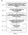
- FIG. 2is a flow diagram illustrating a method for making a device according to another embodiment of the invention.
- FIGS. 3A-3Fdepict a series of vertical cross-sectional schematic diagrams illustrating one possible sequence of steps for carrying out the method of FIG. 2 .
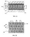
- FIG. 4Adepicts a scanning electron microscope (SEM) image of a vertical cross-section of a nanostructured alumina template.
- FIG. 4Bdepicts a scanning electron microscope (SEM) image of a horizontal cross-section of a nanostructured alumina template.
- Active Layergenerally refers to the layer within a photovoltaic or solar cell device where conversion of radiant energy to electrical energy takes place.
- Anodizationrefers to the formation of a film, such as an oxide, on a conducting material, such as a metal, by electrolysis.
- Arrayrefers to a regular arrangement of objects or structures over a scale of distance greater than some characteristic dimension of a typical structure or object in the array.
- Aspect Ratiorefers to the ratio of pore height or depth to pore width.
- Band Gaprefers to the energy difference between the HOMO and LUMO levels (or between the conduction valence bands) in a charge transfer material or semiconductor.
- Buckminsterfullerene or Fullerenerefers to molecular cages consisting, e.g., of only carbon atoms or mostly carbon atoms. The arrangement of the atoms is almost exclusively in the form of hexagons and pentagons. For example, 12 pentagons and 20 hexagons make a C 60 cage, which is 10 ⁇ in diameter, with a 4- ⁇ cavity. Fullerenes also have other useful forms, such as C 20 , C 36 , C 60 , C 70 , C 76 , C 84 , etc. Buckminsterfullerene/Fullerenes include derivatives such as doped, functionalized (e.g.
- solubilized fullerenese.g., phenyl-C 61 -butyric acid methyl ester (PCBM), and derivatives thereof, and polymerized fullerenes or combinations thereof as well as fullerene-like molecular cages with or without carbon.
- PCBMphenyl-C 61 -butyric acid methyl ester
- Charge-transfer Materialgenerally refers to a semiconductor, such as a n-type electron acceptor or an p-type hole acceptor.
- a first and second semiconductor materialsare said to have complementary charge-transfer properties with respect to each other when the first material is a hole-acceptor and/or hole-transporter with respect to the second and the second is an electron-acceptor and/or electron-transporter with respect to the first or vice versa.
- Two materialscan have complementary charge-transfer properties if they have different electron affinities.
- Conerefers to shape having symmetry about an axis and a tapering cross-section.
- Cylinderrefers to a shape having symmetry about an axis and a substantially constant cross-section.
- the efficiencyis the ratio of energy output (e.g., in the form of electrons) to the necessary energy input (e.g., in the form of photons).
- Electrochemicalrefers to the process of driving a chemical reaction by passing an electric current through a reaction mixture.
- Electrolysisrefers to the process of driving a redox reaction in the reverse by passing an electric current through a reaction mixture.
- Element Spacingrefers to the distance between neighboring template elements measured e.g., in terms of the number of elements per unit area, center-to-center distance between elements or, in the case of pore-like elements, wall thickness.
- Elongated Structuresrefers to geometrical shapes such as tubes, pillars, free-standing pillars, cylinders, needle- or whisker-like elongated crystals, protruding from a surface, as well as openings such as pores, and channels, e.g., generally hollow and substantially straight vertical openings, formed into or through a layer of material.
- Hole-Acceptor and electron-acceptorare relative terms for describing charge-transfer between two materials.
- a first materialhas a valence band edge or highest occupied molecular orbital (HOMO) that is higher than the corresponding valence band edge or HOMO for a second material
- the first materialhas a conduction band edge or lowest unoccupied molecular orbital (LUMO) that is higher than the corresponding conduction band edge or LUMO for the second material
- the first materialis a hole-acceptor with respect to the second material and the second material is an electron-acceptor with respect to the first material.
- a particular band edge or molecular orbitalis said to be “higher” when it is closer the vacuum level.
- Hybrid Organic-Inorganicwith respect to photovoltaic devices and solar cells, refers to a device that uses both organic and inorganic materials either within a layer, in different layers or some combination of both.
- Inorganic MaterialsMaterials which do not contain carbon as a principal element. Examples include metal-oxides and mixed metal oxides. These include both conductive materials (e.g. oxides such as titania, ITO, SnO x , F-doped SnO x , Al-doped ZnO x , ZnO x , etc.) and non-conductive materials such as AlO x , SiO x , etc.
- conductive materialse.g. oxides such as titania, ITO, SnO x , F-doped SnO x , Al-doped ZnO x , ZnO x , etc.
- non-conductive materialssuch as AlO x , SiO x , etc.
- Layerrefers to a feature characterized by a substantially greater length and/or width compared to its thickness.
- a layermay be composed of multiple elements in a substantially two-dimensional array or two or more sub-layers stacked on top of one another or some combination of both.
- Nanostructuredgenerally refers to the property of having features with a characteristic dimension on the order of several nanometers (10 ⁇ 9 m) up to ten's of nm across.
- Organic MaterialsCompounds, which principally consist of carbon and hydrogen, with or without oxygen, nitrogen or other elements, except those in which carbon does not play a critical role (e.g., carbonate salts). Examples of organic materials include:
- Organic Solar CellA type of solar cell wherein an active photoelectric layer is fabricated, either partly or entirely, using organic materials, e.g., polymers, oligomers, molecules, dyes, pigments (including mixtures).
- Photovoltaic DeviceA device that absorbs radiation and coverts energy from the radiation into electrical energy. Solar cells are examples of photovoltaic devices.
- RadiationEnergy which may be selectively applied including electromagnetic energy having a wavelength between about 10 ⁇ 14 and about 10 4 meters including, for example, gamma radiation, x-ray radiation, ultraviolet radiation, visible light, infrared radiation, microwave radiation and radio waves.
- semiconductorgenerally refers to a material characterized by an electronic band gap typically between about 0.5 eV and about 3.5 eV.
- Solar CellA photovoltaic device that interacts with radiation (often in the form of sunlight) impinging on the device to produce electric power/voltage/current.
- Template Elementrefers to a topological feature formed in a layer of template material.
- Template Porerefers to a pore formed in a layer of template material.
- Tubulerefers to a hollow tube-like structure.
- a tubulecan be formed, e.g., within a template element, such as a pore or channel, in which case the tubule can have a symmetry axis aligned substantially along the symmetry axis of the template element.
- Tubule Porerefers to a central hollow space within a tubule that is substantially aligned along the symmetry axis of the tubule.
- a photovoltaic deviceis built from an inorganic insulating nanostructured template.
- a first charge-transfer materialcoats the walls of the template elements leaving behind additional space.
- An optional conductive coatingmay be applied to the insulating nanostructured template before it is coated with the first charge-transfer material.
- a second (complementary) charge-transfer materialsfill the additional space such that the first and second charge-transfer materials volumetrically interdigitate. At least one of the charge-transfers materials absorbs light or other radiation.
- the first and second charge-transfer materialsare n-type and p-type semiconducting materials.
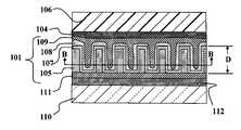
- FIGS. 1A-1Bdepicts a portion of a photovoltaic device 100 according to an embodiment of the present invention.
- the device 100generally includes an active layer 101 disposed between two electrodes e.g., a base electrode 110 and a transparent conducting electrode (TCE) 106 (or vice versa).
- An optional interface layer 104may be disposed between the active layer 101 and the TCE 106 .
- a semiconducting or conducting underlayer 111may optionally be disposed between the active layer 101 and the base electrode 110 .
- the underlayer 111may be a metal foil such as stainless steel, aluminum or titanium that may serve as an etch-stop or anodization stop layer.
- the underlayer 111may be a layer of titanium oxide or zinc oxide or other metal oxide.
- the TCE 106 and base electrode 110may be conductive electrodes or they could include non-conductive materials that provide support, e.g., for conductive layers that serve as the actual electrodes.
- the base electrode 110may be in the form of a commercially available sheet material such as such as C-, Au-, Ag-, Al-, or Cu-coated Steel or Al foil, or metal/alloy-coated plastic foils, including metal or metallized plastic substrates/foils that may be optionally planarized to reduce surface roughness.
- the base electrodemay be pre-patterned (or patterned at a suitable stage during device fabrication) to facilitate parallel and/or series wiring of individual devices as commonly used in the fabrication of PV cell modules. In this context, pre-patterning can result in individual electrically insulated base electrode segments.
- the base electrode 110may alternatively be made from a transparent conducting material, e.g., indium tin oxide and the like disposed, e.g., on a glass or plastic substrate.
- the TCE 106may be a layer of transparent conducting oxide (TCO) such as indium tin oxide (ITO) or fluorinated tin oxide (F:SnO 2 ).
- TCOtransparent conducting oxide
- ITOindium tin oxide
- F:SnO 2fluorinated tin oxide
- the TCE 106may optionally include (either with or without a TCO) some combination of a transparent conducting polymer, a thin metal layer or an array of spaced apart wires, e.g., in the form of a mesh, grid or parallel wires.
- the optional interface layer 104may be a short-proofing barrier layer or an organic material such as a conducting polymer.
- Suitable organic materialsinclude PEDOT (Baytron), or polyaniline doped with a dopant such as polystyrene sulfonic acid (PSS).
- the interface layer 104is poly-3,4-ethylenedioxythiophene-polystyrenesulfonic acid (PEDOT-PSS).
- both the TCE 106 and base electrode 110may be transparent. It is also possible to switch the locations of the TCE 106 and base electrode 110 .
- the active layer 101includes a nanostructured insulating template 105 , an optional conductive layer 107 , and first and second charge-transfer materials 108 , 109 . It is often desirable that the template 105 be made from a material that is transparent in the visible and near IR light ranges. In a preferred embodiment, the porous template is made of an insulating material such as alumina (aluminum oxide) or other insulating materials.
- the template 105may be formed by oxidizing a layer of metal 112 (e.g., aluminum) disposed on a surface of the base electrode 110 . For purposes of illustration, a portion of the metal layer 112 is shown between the template 105 and the base electrode 110 .
- a metal layere.g., aluminum
- a metal layermay be partially anodized so that the base electrode 110 and template 105 are both formed from the same metal layer.
- the template 105contains template elements 103 , which may be distributed in a substantially uniform fashion, although exact uniform spacing, shape or size are not strictly required.
- the template elements 103can be elongated structures, including, but not limited to, tubes, channels, pores, pillars, and the like, that may be substantially cylindrical in shape.
- the template elements 103can have a cone-like shape, e.g., truncated cones tapering with the wider end furthest from to the layer of metal 112 , i.e., towards the top of the drawing in FIG. 1A .
- the cone-like shapemay also be reversed, i.e., with the wider openings being at the bottom and the narrower openings at the top.
- the template elements 103are in the form of nanotubes, e.g., hollow tubes with spaces between the sidewalls of the tubes.
- the template elements 103can be characterized by an average element spacing A, an average wall thickness B, and an average diameter C.
- the average spacing Acan be measured, e.g., from center-to-center, and can range from about 10 nm to about 500 nm.
- the tubescan protrude 50 nm to 2000 nm above the template 105 .
- Such tubescan have diameters ranging from 1 nm to 500 nm, with tube walls up to 50 nm thick.
- the average wall thickness Bcan range from less than about 5 nm to about 50 nm.
- the average diameter Ccan be in the range of several tens of nanometers to several hundred nanometers. For example, it is possible to form pores or tubes as small as about 2 nm to as large as about 500 nm in diameter.
- the density of the template elements 103can range from about 10 12 elements per square meter to about 10 16 elements per square meter. For template elements of a given diameter C and densities greater than about 1/C 2 the elements tend to overlap and merge with one another, although some degree of overlapping/merging may be acceptable. Also, the diameter C may be larger than the wall thickness B between neighboring template elements 103 .
- the template 105may be further characterized by a thickness D.
- the thickness Dmay be the thickness of the entire metal layer 112 , if it is oxidized entirely, or the thickness of the portion that is oxidized.
- the template 105is relatively thin.
- the thickness Dmay be from about 50 nm to about 2000 nm (2 microns) thick.
- the insulating template 105may optionally be coated with a conductive material 107 , such that the conductive material 107 is disposed between the insulating template 105 and the first charge-transfer material 108 .
- the conductive material 107may be deposited over the template elements 103 in a substantially conformal fashion so as to allow a continuous connection between the elements 103 and the underlying bottom electrode 110 .
- the template 105is made of an insulating material such as alumina (and sometimes when it is not), it may be necessary to remove a barrier layer from the bottoms of the template elements 103 so that the first charge-transfer material 107 can make electrical contact with the underlayer 111 and/or metal layer 112 and/or base electrode 110 .
- the conductive material 107may be an inorganic material such as indium tin oxide, indium oxide, tin oxide, fluorinated tin oxide, Preferably, the conductive material 107 is a thin layer (e.g., about 1 nm to about 100 nm) of an electrically conductive material.
- the conductive material 107may be a conductive oxide such as tin oxide (SnOx), indium oxide (InOx), fluorinated tin oxide (F:SnOx), indium tin oxide (ITO), tungsten oxide, titania (titanium oxide, TiO 2 ), zinc oxide (ZnO) (with or without Al doping), zirconium oxide, lanthanum oxide, niobium oxide, tungsten oxide, strontium oxide, calcium/titanium oxide, vanadium oxide, zirconium oxide, molybdenum oxide, as well as blends or alloys of two or more such materials.
- the conductive material 107may be a layer of a metal, such as titanium.
- the conductive material 107may be a thin layer of an organic material such as PEDOT:PSS, doped conjugated organic materials, doped fullerenes, e.g., doped C 60 , and the like.
- the first charge-transfer material 108coats the template elements 103 in a way that leaves behind additional space not occupied by the first charge-transfer material 108 .
- the second charge-transfer material 109fills the additional space and does not protrude substantially out of the template 105 .
- the second charge-transfer material 109may fill the hollow spaces in the centers of the nanotubes and empty space between the tubes such that the first and second charge-transfer materials are volumetrically interdigitated. It is often desirable that the first and second charge-transfer materials do not extend significantly beyond the surface of the nanostructured template 105 .
- the first and second charge transfer materials 108 , 109may fill space between and/or within the template elements 103 up to a level that is substantially even with an upper surface of the template 105 .
- at least a part of the first charge-transfer material 108is connected to the bottom of the elements 103 to provide electrical contact, i.e. a charge carrier path, between the first charge-transfer material 108 and the base electrode 110 or optional underlayer 111 .
- the first and second charge-transfer materials 108 , 109have complementary charge-transfer properties with respect to each other.
- one of the first and second charge-transfer materials 108 , 109may be regarded as an electron acceptor while the other may be regarded as a hole acceptor.
- Charge-transfer materialsmay be characterized by a lowest unoccupied molecular orbital (LUMO) or conduction band and a highest occupied molecular orbital (HOMO) or valence band as indicated schematically in FIG. 1C . Where two charge transfer materials with different energy levels meet at an interface INT electrons e ⁇ tend to move across the interface INT from the higher LUMO or conduction band to the lower LUMO or conduction band.
- holes h+tend to move across the interface INT from the lower HOMO or valence band to the higher HOMO (or valence band). Note that it is possible for a given material to be a hole acceptor with respect to one material and an electron acceptor with respect to another material.
- a lowest unoccupied molecular orbital (LUMO) or conduction band of the first charge-transfer material 108differs from a LUMO or conduction band of the second charge-transfer material 109 by more than about 0.2 eV.
- at least one and possibly both charge-transfer materialsabsorb light or other radiation from some portion of the electromagnetic spectrum. More specifically, it is also desirable for at least one of the charge transfer materials 108 , 109 to have an absorbance of greater than about 10 3 /cm at the peak of absorption, more preferably, greater than about 10 4 /cm at the peak of absorption.
- the first charge-transfer material 108may coat the walls and bottoms of the template elements 103 and the second charge-transfer material 109 coats the first charge-transfer material to form tubules with the additional space being in the form of tubule pores.
- the second charge-transfer material 109may fill the tubule pores.
- Each tubulemay be characterized by an outside diameter roughly equal to the inside diameter of the corresponding template elements 103 .
- Each tubule poremay be characterized by a tubule pore diameter d ranging from about 1 nm to about 500 nm. In general the tubule pore diameter d is less than the template pore diameter C.
- the tubulesmay have a tubule wall thickness of up to about 100 nm and a total tubule height of up to up to about 2 microns.
- the first and second charge-transfer materials 108 , 109may be blended together in a blend that fills template elements 103 .
- the tubule pore diameter dmay represent an inner diameter for a tubule of the first charge-transfer material 108 .
- the outer diameter for the tubuleis essentially the template structure diameter C, less the thickness of the optional conductive layer 107 , if it is present.
- the tubulemay have a wall thickness given by the half the difference between the inner and outer tubule diameters, i.e., (C-d)/2.
- the tubule wall thicknessmay range from about 0.5 nm (5 Angstroms) to about 20 nm, preferably from about 0.7 nm to about 15 nm, more preferably about 10 nm, and most preferably about 5 nm.
- the tubule diameter Cmay be about 40 nm
- the tubule pore diameter dmay be about 30 nm
- the first charge-transfer material 108may be an inorganic semiconducting material.
- suitable inorganic materialsinclude, e.g., metal oxides such as titania (TiO 2 ), zinc oxide (ZnO), copper oxide (CuO or Cu 2 O or Cu x O y ), zirconium oxide, lanthanum oxide, niobium oxide, tin oxide, indium oxide, indium tin oxide (ITO), vanadium oxide, molybdenum oxide, tungsten oxide, strontium oxide, calcium/titanium oxide and other oxides, sodium titanate, potassium niobate, cadmium selenide (CdSe), cadmium suflide (CdS), copper sulfide (e.g., Cu 2 S), cadmium telluride (CdTe), cadmium-tellurium selenide (CdTeSe), copper-indium selenide
- metal oxidessuch as titania (Ti
- the first charge-transfer material 108may be an organic p- or n-type material e.g. fullerenes or modified/functionalized fullerenes (e.g. PCBM).
- the first charge-transfer material 108may or may not absorb a substantial fraction of the incident light.
- the second charge-transfer material 109may be an organic material.
- the second charge-transfer material 109is an organic material that absorbs light in the bulk of the material.
- suitable organic materialsinclude conjugated polymers such as poly(phenylene) and derivatives thereof, poly(phenylene vinylene) and derivatives thereof (e.g., poly(2-methoxy-5-(2-ethyl-hexyloxy)-1,4-phenylene vinylene (MEH-PPV), poly(para-phenylene vinylene), (PPV)), PPV copolymers, poly(thiophene) and derivatives thereof (e.g., poly(3-octylthiophene-2,5,-diyl), regioregular, poly(3-octylthiophene-2,5,-diyl), regiorandom, Poly(3-hexylthiophene-2,5-diyl), regioregular, poly(3-hexy
- suitable polymersinclude organometallic polymers, polymers containing perylene units, poly(squaraines) and their derivatives, and discotic liquid crystals.
- suitable organic materialsinclude organic pigments or dyes, azo-dyes having azo chromofores (—N ⁇ N—) linking aromatic groups, phthalocyanines including metal-free phthalocyanine; (HPc), perylenes, perylene derivatives, Copper pthalocyanines (CuPc), Zinc Pthalocyanines (ZnPc), naphthalocyanines, squaraines, merocyanines and their respective derivatives, poly(silanes), poly(germinates), 2,9-Di(pent-3-yl)-anthra[2,1,9-def:6,5,10-d′e′f]diisoquinoline-1,3,8,10-tetrone, and 2,9-Bis-(1-hexyl-hept-1-yl)-anthra[2, 1,
- the first and/or second charge-transfer materials 108 , 109may also include polyfluorenes and polyfluorene-based copolymers and blends, e.g. co-polymerized and/or blended with charge transporting (e.g. tri-phenyl-amines and derivatives) and/or light-absorbing compounds (e.g. fused thiophene rings and derivatives, generally hetero-atom ring compounds with or without substituents), pigments, dyes, or fullerenes.
- the second charge-transfer material 109can include fullerenes.
- the first charge-transfer material 108is a thin layer (e.g., about 1 nm to about 100 nm, more preferably about 10 to about 50 nm) of amorphous silicon (a-Si), which is a well-known thin-film PV material.
- a-Siamorphous silicon
- deposition technologiese.g. sputtering, ALD, CVD, PECVD, MOCVD etc., have been developed and several of these are widely in use to deposit a-Si films.
- Several of these methodshave the potential to deposit doped or undoped a-Si films not just on surfaces but down high aspect ratio holes (e.g. via-holes).
- amorphous Sihas a low absorption coefficient.
- Prior art amorphous Si PV cellstypically employ film thicknesses in excess of 1 micron and often significantly more.
- a-Siis the main active layer in a prior art PV cell
- lightis absorbed in the a-Si layer, which has been shown to degrade, in particular upon exposure to UV light.
- Organic and organic-inorganic hybrid solar cellstypically rely on the absorption of light in an organic, creating an exciton, followed by the splitting of the exciton into a positive and negative charge carrier at an exciton-splitting interface.
- a high surface area of the exciton-splitting interface and preferably a short path for negative and/or positive charge carrier to their respective charge-collecting electrodeare desirable.
- a-Si (p- or n-type but in particular n-type)/organic hybrid solar cellshave not been made in the prior art.
- a film of titania particlesmay be coated with a-Si. It would be difficult to completely and efficiently deposit a-Si in the narrow channels after sintering a film of randomly arranged titania particles.
- a flat a-Si/organic cellwould have a limited exciton-splitting interface. It may be beneficial for a PV cell with e.g. homogeneous organic layers or all-organic blends to be put on an a-Si layer instead of straight onto a charge-carrier-collecting electrode.
- the second charge-transfer material 109could also be an inorganic material.
- the a-Si coatingcould be made thicker in a ‘coarser’ template 105 to provide some (perhaps a more significant) light-absorption function.
- the first charge-transfer materialis n-type doped a-Si and the second charge-transfer material 109 is a p-type organic material.
- a thin coating of a-Sican be largely transparent.
- an a-Si coating deposited on the walls of the template elements 103by standard deposition methods, e.g., sputtering, CVD, PECVD and the like. The cost of deposition with these techniques is highly correlated with deposition time. Fortunately, thin coatings (e.g., about 1-100 nm) can be deposited with these techniques in relatively short deposition times.
- the first charge-transfer material 108is made of a-Si, and sometimes when it is not, the first charge-transfer material 108 may be thicker at an upper portion of the nanostructured template 105 , e.g., closer to the TCE 106 than at a lower portion of the template 105 , e.g., closer to the base electrode 110 .
- the thickness of the first charge-transfer material 108is substantially uniform throughout the coated template 105 to within about 100% (e.g., 20 mm thick at the top and 10 nm thick at the bottom). More preferably, the thickness of the first charge-transfer material is uniform to within about 50%.
- insulating aluminamay be used as the template 105 (with a bottom barrier layer removed and/or reduced to render it conductive) because the doped a-Si layer would also provide the conductive path.
- the conductive layer 107may not be necessary.
- the second charge-transfer material 109may be an organic material having a band gap that is less than about 2 eV or less than about 1.7 eV.
- the dominant negative charge carrier energy levels of the second charge-transfer material 109can lie within 1 eV but better within 0.5 eV of the a-Si conduction band/.
- the dominant negative charge carrier energy level of the second charge-transfer material 109is less than 1 eV and preferably 0.5 eV above the a-Si conduction band/states and a HOMO level (or equivalent p-type charge carrier transporting level) of the second charge-transfer material 109 is above that of the a-Si valence band.
- the choice of materialsmay affect whether the resulting device 100 has the desired energy levels.
- the first charge-transfer material 108is a-Si, thiophene-, fluorine- or aryl-vinyl-based polymers, copolymers or blends may be used as the second charge-transfer material 109 .
- the a-Si layermay be suitably doped by e.g. carbon or germanium.
- the a-Si layer employed in certain embodiments of the present inventioncan and would typically be hydrogenated.
- the a-Si layer(with the employed level of doping, hydrogenation, etc.) may be optionally treated (chemically, wet-chemically—e.g. via an HF etch) prior to deposition of the second charge transfer material 109 (or an optional interfacial layer 113 —see below) in order to remove potential a-Si surface oxide layers.
- the surface of the a-Simay also be passivated to protect it from a surface oxide layer growth and/or to enhance exciton splitting and/or charge transfer and/or reduce undesired exciton recombination.
- an optional interfacial layer 113may be disposed between the first and second charge-transfer materials 108 , 109 as shown in FIG. 1D .
- the interfacial layer 113may enhance the performance of the device 100 .
- the interfacial layer 113may be configured to enhance the efficiency of the device 100 in the form of one or more of (a) differential charge-transfer, i.e., charge-transfer between the two materials that exhibits different rates for forward versus backward transport; (b) differential light absorption to extend a range of wavelengths that the active layer can absorb; or (c) enhanced light absorption and/or charge injection. Examples of such interfacial layers are described in detail in commonly assigned U.S. patent application Ser. No. 10/419,708, the entire disclosures of which are incorporated herein by reference.
- the interfacial layer 113may contain organic materials attached onto (not below) the first charge-transfer material 108 .
- organic materialsinclude fullerenes (e.g., C 60 , C 70 and the like, either chemically functionalized or non-functionalized), carbon nanotubes, dyes, ruthenium dyes, pigments, and organic monomers, oligomers, and polymers, any of which may be deposited singly or in combination onto the first charge-transfer material 107 .
- the second charge-transfer material 108can be a monolayer or multi-layer interfacial layers may be used as well.
- the interfacial layer 113may be in the form of individual molecules, monomers or oligomers or a continuous or substantially continuous layer between the first and second charge-transfer materials 108 , 109 .
- the choice of material for the interfacial layer 113may depend on the materials used for the first charge-transfer material 108 and the second charge-transfer material 109 .
- the first charge-transfer material 108is a-Si
- well-known ‘electron-channel/absorbing’ dyessuch as rubidium dyes can be included in the interfacial layer 113 between the first and second charge-transfer materials 108 , 109 .
- Such dyesmay have a LUMO level very close to that of a-Si.
- Doped (or undoped) fullerenes such as C 60can also be functionalized, e.g., so that they can be attached covalently to the first charge-transfer material 108 .
- the carbon layers in fullerenes such as C 60may be curved due to inclusion of five-membered rings considerable strain energy in the fullerenes is reduced when the carbon atoms of a C ⁇ C double bond are replaced by two sp3-hybridized carbon atoms. This can be exploited for functionalization of the fullerenes by addition reactions.
- the interfacial layer 113may also include chemicals that can covalently attach to the first charge-transfer material 108 , e.g., a silane, and thus change the surface energy and/or bonding trap-states and/or attach to dangling-bonds at an exposed surface of the first charge-transfer material 108 and/or introduce a dipole layer that may increase the efficiency for charge extraction and/or reduce detrimental charge recombination.
- Examplesare functionalization with benzoic, various carboxylic acid-group-containing compounds and other acids, tert-butyl-pyridine, surfactants, dye molecules, silanes and silicon compounds or their functionalized derivatives that are often used as adhesion-promoters.
- the surface of the first charge-transfer material 108may also be functionalized with silylating agents for modulation of surface properties, and/or for introduction of functional groups (amine group, aliphatic group, hydroxyl, carboxylic etc.) for further surface derivitization.
- interfacial layer 113may be a layer of C 60 or other fullerenes functionalized with a carboxylic acid moiety combined with hydroxylating a metal oxide first charge-transfer material 108 to produce preferential charge flow into or out of the first charge-transfer material 108 .
- the conductive layer 107 and/or the first and/or second charge-transfer materials 108 , 109may generally include other organic materials, e.g., a conjugated polymer coating the first charge-transfer material 108 .
- the nanostructured template 105could be sequentially coated with different layers of conjugated polymer or other organic materials, which are then melt-infiltrated to create, via surface energy effects, the desired layered or blended structure of the first and second charge-transfer materials 108 , 109 .
- first charge-transfer material 108 and/or interfacial layer 113may be created by self-assembly or electro-static self-assembly of materials such as PEDOT:PSS or other materials deposited from ionic/charged polymer solutions (e.g. tetra-hydro-thiophene precursor poly-phenylene-vinylene and derivatives).
- first and second charge-transfer materials 108 , 109are described as being respectively an inorganic material and an organic material, it is possible to make the active layer 101 with the first charge-transfer material 108 organic and the second charge-transfer material 109 inorganic or with both charge-transfer materials 108 , 109 being organic.
- cone-like porescan be created that can have certain charge transport advantages.
- Such cone-like poresare a variant of the pores shown in FIGS. 5A-1B above.
- pore-widening or ‘cone-shaping’could also be done by other methods such as plasma-etching, reactive-ion-etching (RIE), anisotropic RIE.
- RIEreactive-ion-etching
- ‘Cone-shaping’ the template elements 103may facilitate the coating of the nanostructured template 105 with e.g.
- the first charge-transfer material 108(and/or interfacial layer 113 and/or optional conductive layer 107 as described above), particularly when the deposition method for the first charge-transfer material 108 and/or interfacial layer 113 is e.g. sputtering, evaporation or similar deposition process. Care should be taken to avoid clogging the pores at the top before the rest is filled or coated. Cone-shaping may prevent the ‘clogging’ of both template pores and tubule pores at various fill-stages (e.g., for filling the template elements 103 with the first charge-transfer material 108 and/or the interfacial layer 113 and/or filling the tubule pores 102 with the second charge-transfer material 109 ).
- the conductive material 107may be a layer of a conductive transparent oxide (such as ITO or F:SnO 2 ) deposited via ALD or PECVD or CVD or sputtering on top of a nanostructured template 105 made of anodized alumina.
- the ITOmay then be covered with a layer of n-type semiconducting titania as the first charge-transfer material 108 , deposited via ALD or CVD or sputtering, which may then be solution-coated with an (optional) thin layer of functionalized C 60 (C 60 —COOH, PCBM, or similar materials) as the interfacial layer 113 between the first and second charge-transfer materials.
- a conductive transparent oxidesuch as ITO or F:SnO 2
- the ITOmay then be covered with a layer of n-type semiconducting titania as the first charge-transfer material 108 , deposited via ALD or CVD or sputtering, which may then be
- the second charge-transfer material 109may be a layer of organic polymer deposited by solvent vapor deposition or a solution based deposition technique.
- a small organic moleculesuch as pentacene could be vapor deposited or evaporated into the nanostructured template 105 using a standard organic evaporation method, or a soluble Pentacene precursor could be solution-deposited into the template, after which the Pentacene precursor could be converted to Pentacene through annealing.
- the first charge transfer material 108may be an n-type semiconductor coating material (e.g. titania or ZnO or other metal oxide) that may be coated onto a template 105 made of alumina that has been anodized down to an underlying titania or other n-type underlayer 112 .
- the second charge-transfer material 109may be a layer of organic polymer deposited by solvent vapor deposition or a solution based deposition technique.
- a small molecule such as pentacenecould be evaporated into the nanostructured template 105 using a standard organic evaporation method, or a soluble Pentacene precursor could be solution-deposited into the template, after which the Pentacene precursor could be converted to Pentacene through annealing.
- the conductive material 107may be an n-type semiconductor coating material (e.g. titania or ZnO or other metal oxide) that may be coated onto a template 105 made of alumina that has been anodized down to an underlying titania or other n-type underlayer 112 .
- the first charge-transfer material 108may be a layer of n-type a-Si deposited by chemical vapor deposition, metal-organic chemical vapor deposition, evaporation, sputtering, atomic layer deposition, etc. conductive material 107 .
- the second charge transfer material 109may be an organic or inorganic p-type material, e.g., such as those described above.
- the conductive material 107may be coated onto a template 105 of alumina and into elements 103 in the form of alumina tubes that have been created/anodized down to an underlying titania or other n-type underlayer 112 .
- the tube heightmay be as great as 2000 nm.
- the tube widthmay be as wide as 500 nm, more typically about 300-500 nm, or possibly as small as 50 nm or less.
- the conductive material 107may be deposited for example by atomic layer deposition (ALD).
- the first charge transfer material 108may be a 50 nm layer of n-type CdS deposited at the base and along the sidewalls of the tubes, e.g., by electrodeposition or chemical bath deposition.
- a second charge-transfer material 109such as p-type CdTe, CdSe or Cu 2 S may then be deposited into the tubes for example by electrochemical techniques.
- the template 105 and base electrode 110may be made from the same layer of metal, e.g., by partial anodization as described above, it may be desirable to dispense with the underlayer 111 and instead coat the bottoms of the template elements 103 with a conductive or semiconductive material similar to that of the underlayer 111 after removing a barrier layer, if any.
- the conductive or semiconductive material at the bottoms the template elements 103may not be necessary if the first charger transfer material 108 , conductive layer 107 (if any) or an interfacial layer 113 (if any) would otherwise make sufficient electrical contact with the bottom electrode 110 .
- first and second charge-transfer materials 108 , 109may be entirely inorganic, e.g. a inorganic multilayer that fills template structures 103 or the space unoccupied by the conductive material 107 if it is present.
- FIG. 2depicts a flow diagram illustrating an example of such a method 200 . Examples of how the method might be carried out are depicted in the sequences of cross-sectional diagrams depicted in FIGS. 3A-3M .
- the method 200begins at 202 by forming a nanostructured template, e.g., by anodizing a layer of metal, e.g., a metal substrate or a substrate with at least one metal coating, having an array of template elements distributed in a substantially uniform fashion.
- the template elementsmay optionally be coated with a conductive material.
- a first charge transfercoats the template elements leaving behind additional space.
- a second (complementary) charge-transfer materialsfill additional space not occupied by the first charge-transfer material. Electrodes may optionally be added at 210 and the resulting device may optionally be encapsulated at 212 .
- a porous templatecan be anodized from a layer of metal (e.g., aluminum) 312 disposed on a substrate 310 .
- metale.g., aluminum
- an oxide film 305can be formed at the metal surface as shown in FIG. 3B .
- An array of template elements 303can be formed in the oxide film 305 , while the oxide film 305 is created.
- material at the bottom of the template elements 303can be removed by chemical means or by incrementally stepping down the voltage. Where a portion of the metal layer 312 remains between the oxide film 305 and the substrate 310 , the material at the bottom of the template elements 303 can be chemically removed or can be left in place (e.g., as an electrode).
- the anodizing voltagecontrols pore size and pore density, and the total amount of charge-transferred determines film thickness.
- aluminumcan be treated anodically in a phosphoric acid electrolyte. Examples of nanostructured alumina templates made in this way are depicted in the SEM images of FIG. 4B and FIG. 4C .
- the SEM images of FIGS. 4A and 4Balso illustrate an example of template pores distributed in a substantially uniform fashion.
- the preferred thickness range for the metal layer to be anodizedis from about 100 nm to about 2 microns, preferably in the 200-nm to 600-nm range, and more preferably about 300 to 500 nm. Porous templates in these thickness ranges provide useful depths for proper optoelectronic function in the resulting PV device.
- the metal substratee.g. aluminum
- its porous metal oxide equivalente.g., alumina
- the anodization voltage, current, acid concentration, anodization time, and temperaturecan be adjusted to improve pore formation in a metal film whose initial thickness ranges from (for example) 150 to 250 nm.
- the anodization voltage, current, acid type, acid concentration, electrolyte additives, anodization time, and temperaturecan be adjusted to provide for a porous template with specific target dimensions.
- Structure sizes in such filmstypically range from 10 to 450 nm, though it is also possible to form template elements as small as 2 nm and as large as 500 nm.
- the typical density of template elementsis about 10 12 to about 10 16 elements per square meter.
- a film thickness of 100 to 500 nanometersis generally achieved, though films can be formed whose thickness is as small as 10 nm and as great as 50-100 microns.
- Al metale.g., 99.99% pure
- a glass or metal foil substrateby use of evaporation, e-beam evaporation, sputtering, or the like.
- an Al foilmay be commercially purchased from any of a variety of vendors.
- the filmmay be anodized by treatment at 1-250V for a specified time, e.g., on the order of several minutes, in 5-10% H 3 PO 4 below 10° C. For example, in 75 min, an aluminum oxide film of roughly 30 microns thick can be generated.
- the potential voltagemay range from about 1V to about 250V.
- the preceding protocolmay result in porous alumina template elements in the form of pores or tubes in the diameter range of about 10-450 nm.
- the anodized material at the base of the poresmay be perforated by stepping down the anodizing voltage, e.g., from 100V to 0.1 V is greater.
- the barrier layer at the base of the template tubesmay be removed using chemical etching, for example using an acidic bath that promotes pore-widening.
- anodized specimensare then immersed in a 5% (vol) phosphoric acid solution at 30° C.
- the anodized material at the base of the poresmay be made conducting by a suitable reduction reaction.
- the porous templateby anodizing a metal layer to form an oxide film on glass, ITO-coated glass, F:SnO 2 coated glass, ITO coated PET or other plastic, or other coated or non-coated metal foils as well as metallized plastics.
- the substrate 310may be a sheet of glass or plastic or metal or a continuous foil of metal or plastic with a base electrode.
- the base electrodetransparent or otherwise
- the substrate/base-electrode 310may be covered with a metal (e.g., aluminum) layer composed of the to-be-anodized aluminum.
- Nanostructured templatesmay also be made by a reactive ion etching technique using an anodized porous template as an etch mask. Such techniques are described e.g., in U.S. patent application Ser. No. 10/719,042, filed Nov. 21, 2003, which is incorporated herein by reference. Nanostructured templates can also be made by surfactant temptation techniques such as those described in commonly assigned U.S. patent application Ser. Nos. 10/290,119, 10/303,665 and 10/319,406, which are incorporated herein by reference. Referring to FIG. 3A an underlayer 311 may be disposed between the substrate/base electrode 310 and the subsequent layers, e.g., the metal layer 312 that is to be anodized, etc.
- the underlayer 311may be a metal layer that can act as an ‘anodization-stop layer’ and/or may act as an etch-stop layer for the tube- or pore-widening and bottom barrier layer removal etch process.
- the underlayer 311may be a semiconducting layer e.g., titania, disposed between the substrate 310 and the subsequent layers. Such an underlayer can reduce undesired contact between a material filling the template elements 303 and the substrate/base electrode 310 .
- the intermediate layer 311may prevent damage to the underlying substrate 310 (e.g. in case of the base electrode 310 being ITO).
- the substrate 310could be made from a metal or alloy or stainless steel or metallized plastic foil substrate, followed by an intermediate layer, e.g., an etch-stop-layer and/or titania layer, followed by the metal layer 312 that gets anodized to create the nanostructured template 305 .
- the intermediate layer 311e.g. semiconductor or metal
- the template 305 and base electrode 310may be made from the same layer of metal, e.g., by partial anodization as described above, it may be desirable to dispense with the underlayer 311 and instead coat the bottoms of the template elements 303 with a conductive or semiconductive material similar to that of the underlayer 311 after removing a barrier layer, if any.
- a variety of deposition techniquescould be employed to coat the template elements 303 with the first charge-transfer material 308 and/or with the optional conductive layer 307 (and or the layer 311 at the bottom of 305 e.g., by electrodeposition, layer-by-layer deposition or other liquid phase or chemical bath deposition techniques).
- Such techniquesinclude, but are not limited to, electrochemical and electroless (chemical bath) deposition, evaporation, sputtering, plating, ion-plating, molecular beam epitaxy, atomic layer deposition (ALD), plasma-enhanced ALD, electrochemical atomic layer epitaxy, sol-gel based deposition, spray pyrolysis, vapor-phase deposition, solvent vapor deposition, metal-organic vapor phase deposition, metal-organic-vapor-phase epitaxy, atomic layer deposition, chemical vapor deposition (CVD), pulsed CVD, plasma-enhanced CVD (PECVD), metal organic CVD (MOCVD), metal-organic-vapor-phase epitaxy, self-assembly, electro-static self-assembly, melt-filling/coating, layer-by-layer (LBL) deposition, or liquid phase deposition among other techniques.
- electrochemical and electroless (chemical bath) depositionevaporation, sputtering, plat
- the first charge-transfer material 308may be created via deposition or reaction or condensation from the liquid or gas phase or by physical deposition methods. Furthermore the first charge-transfer material 308 may be deposited by electro-deposition, electro-plating, ion-plating, and the like.
- the template 305may be coated with the optional conductive layer 307 by reducing an upper portion of the template 305 to make it electrically conducting.
- the upper portion of an anodized templatemay be reduced by exposing it to a suitable reducing agent to promote a chemical reaction that reduces oxides.
- the conductive layer 307may be formed by depositing material over the nanostructured template 305 .
- some combination of reducing the template 305 and depositing a coatingmay be used to form the conductive layer 307 .
- the first charge-transfer material 308may coat the template elements 303 in a way that forms thin tubules 301 that coat the walls of the template elements 303 as shown in FIG. 3C .
- the tubules 301have tubule pores 302 left behind by the tubule forming process.
- a semiconducting or conducting metal oxidesuch as ITO can be coated on the walls of the template elements 303 , e.g., by sputtering, CVD, atomic layer deposition, or other coating techniques.
- the exposed surface of the first charge-transfer material 308may be subjected to an etch step to remove surface oxides, e.g. by commonly known techniques to remove surface oxide layers from a-Si.
- an etch stepmay be performed either after depositing the first charge-transfer material 308 or before deposition of a subsequent layer or both.
- the template elements 303may alternatively be coated with an organic material such as those listed above with respect to the second charge-transfer material 109 .
- a second charge-transfer material 309may fill parts of the template elements 303 not filled by the first charge-transfer material 308 and/or conductive material 307 as shown in FIG. 3E .
- the first and second charge-transfer materials 308 , 309may be blended together in a mixture and the mixture can fill elements 303 .
- Such blendmay be specifically designed and chosen and/or processed after filling such that a phase-separation occurs in order to promote enrichment of one phase (e.g. the first charge-transfer material 308 ) at the surface of the template 305 (or conductive material 307 ) and the other in the inner area/volume of the template 305 , thus creating a partial or substantial bi-layer structure.
- the second charge-transfer material 309may be an organic material as described above. Such organic materials can be deposited by capillary action, melting, and/or through the assistance of surface energy or osmotic gradients or solvent vapor exposure. Organic polymers and other materials can be used, alone or in combination, at this step, such as those described above with respect to the second charge-transfer material 108 .
- Organic charge-transfer materialscan be applied to the template elements 303 from process solutions, e.g., by any suitable technique, e.g., web-coating, doctor blade coating, spray coating, spin coating, casting, dip-coating or a printing technique such as printing such as screen-printing, ink-jet printing, flexographic printing, gravure printing, micro-gravure printing, and the like.
- Heatmay be applied to the nanostructured network layer and network-filling material during this step, e.g., to evaporate solvents and set the network-filling material and/or to assist material infiltration, e.g., through capillary action and/or assistance of surface energy or osmotic force.
- the organic materialmay be exposed to a solvent vapor to facilitate infiltration into the template elements 303 .
- solvent vapor phase infiltrationare described, e.g., in commonly-assigned co-pending U.S. patent application Ser. No. 10/719,041, entitled “SOLVENT VAPOR INFILTRATION OF ORGANIC MATERIALS INTO NANOSTRUCTURES” filed Nov. 21, 2003.
- the second charge-transfer materialmay include fullerenes (C 60 and C 70 and the like), carbon nanotubes, dyes, ruthenium dyes, pigments, and organic monomers, oligomers, and polymers, any of which may be deposited singly or in combination into the porous template.
- fullerenesC 60 and C 70 and the like
- carbon nanotubesdyes, ruthenium dyes, pigments, and organic monomers, oligomers, and polymers, any of which may be deposited singly or in combination into the porous template.
- organic materialscan be deposited using capillary action and or through osmotic gradients, using liquid solutions containing the materials to be deposited.
- carbon nanotubescan be synthesized directly within the template elements 303 or the tubule pores 302 using, for example, chemical vapor deposition (CVD).
- CVDchemical vapor deposition
- the second charge-transfer material 309may be an inorganic material deposited in the tubule pores by any of several suitable techniques including but not limited to sol-gel chemistry, spray pyrolysis, layer-by-layer deposition (LBL), evaporation, atomic layer deposition (ALD), plasma-enhanced atomic layer deposition (PECVD), chemical vapor deposition (CVD), metal-organic chemical vapor deposition (MOCVD), plasma enhanced chemical vapor deposition (PECVD), sputtering, and the like.
- LBLlayer-by-layer deposition
- ALDatomic layer deposition
- PECVDplasma-enhanced atomic layer deposition
- CVDchemical vapor deposition
- MOCVDmetal-organic chemical vapor deposition
- PECVDplasma enhanced chemical vapor deposition
- sputteringand the like.
- the second charge-transfer materialcould be copper sulfide (Cu 2 S), cadmium telluride (CdTe), zinc telluride (ZnTe), cadmium selenide (CdSe), zinc selenide (ZnSe), cadmium-tellurium selenide (CdTeSe), copper oxide (Cu 2 O or CuO), copper-indium selenide (CdInSe 2 ) or other materials with similar properties.
- the devicecan be finished as shown in FIG. 3F .
- An interlayer 304e.g., a polymer such as PSS:PEDOT may optionally be deposited on top of the second charge-transfer material 309 .
- An electrode in the form of a fine metal grid or thin metal filmcan then be added.
- the final devicemay be encapsulated to provide for mechanical stability and/or protection from the ambient environment.
- a thin metallic film or coatingcan be deposited or attached to the device to serve as an electrode.
- the first charge transporting materials (e.g. 108 ) and the bottom electrode (e.g. 110 )assume the roles of electron-transporter/acceptor/collector and the second material (e.g. 109 ) assumes the role of the opposite positive charge carrier transporter/acceptor/collector and the TCE 106 assumes the role of an anode
- this functional ordercould be reversed.
- the base electrode 110could be an anode.
- the first charge-transfer material 108 and/or interfacial layer 113 and or any additional conductive layers between the template 105 and first charge-transfer material 108could act as positive charge carrier acceptors/transporters/collectors.
- The, e.g., organic (or inorganic) second charge-transfer material 109could be a negative charge carrier acceptors/transporters/collectors, together with the TCE 106 and/or interface layer 104 serving as a cathode.
- the interfacial layer 113is e.g. PEDOT/PSS (acting as anode that contacts down through the template pores to the base electrode 110 ) followed by e.g. a donor/acceptor organic blend filled into the pores or a bi-layer structure with a hole acceptor/transporter layer on top of the interfacial layer 113 with the remaining volume filled with an electron acceptor/transporter.
- the devices described hereinincorporate several advances over prior art devices. Specifically, the devices described herein are solid-state devices that do not contain a liquid electrolyte. Therefore, devices according to embodiments of the present invention are subject to significantly fewer leakage and corrosion problems of the type associated with devices using liquid electrolytes. Furthermore, the devices described herein have a charge splitting layer having with a more uniform and more tunable structure and/or function than prior art devices. In particular, the devices described herein have an active layer characterized by volumetrically interdigitating charge-transfer materials with regularly arrayed template elements having substantially uniform spacing within the plane of the active layer and substantially parallel orientation and uniform length perpendicular to the plane of the active layer. Thus, the charge-splitting layer exhibits a three-dimensional structure that is very regular along its length and width, but also along its depth.
- the devices described hereindo not depend entirely on a monolayer of a dye adsorbed to an n-type inorganic material as a light absorber. Instead, devices according to embodiments of the present invention typically use a p-type light absorber capable of absorbing light in the bulk of the material. Consequently, devices of the type describe herein absorb light more effectively on a volume basis and are more efficient in converting incident light to electrical energy.
- a dyemay optionally be included in the devices described herein, a dye is not needed for the device to convert light into electrical energy, as is the case for dye-sensitized solar cells. Thus, the devices described herein are not “dye-sensitized”.
- devices of the type described hereinmay be made substantially thinner than prior art devices.
- solar cell devices according to embodiments of the present inventionmay be significantly thinner than the typically 8-10 micron thick Graetzel cells or the typically 4-5 micron thick purely inorganic cells.
- the template-filler method of construction described hereinis based on a substantially self-assembling template, that exhibits much greater long-range order.
- the devices described hereindo not use a liquid-based electrolyte or a “redox” chemistry to transport holes away from the light absorbing material. Instead, a p-type organic solid-state material transports holes from the charge splitting interface.
- Embodiments of the present inventionallow for large-scale, low-cost production of photovoltaic devices, such as solar cells or other devices.
Landscapes
- Physics & Mathematics (AREA)
- Chemical & Material Sciences (AREA)
- Engineering & Computer Science (AREA)
- Electromagnetism (AREA)
- Nanotechnology (AREA)
- Crystallography & Structural Chemistry (AREA)
- Inorganic Chemistry (AREA)
- Mathematical Physics (AREA)
- Theoretical Computer Science (AREA)
- Hybrid Cells (AREA)
- Photovoltaic Devices (AREA)
Abstract
Description
- I. Glossary
- II. General Overview
- III. Photovoltaic Device
- IV. Photovoltaic Device Fabrication
- V. Alternative Embodiments
- VI. Conclusion
- (a) Organic Dyes and pigments such as perylenes, phthalocyanines, merocyanines, terylenes and squaraines and their derivatives.
- (b) Polymers: Materials consisting of large macromolecules composed of more than one repeating units. Polymers, composed of 2-8 repeating units are often referred to as oligomers. Examples of such repeating units include, e.g., dyes or pigments.
- (c) Small Molecules, including pthalocyanines (e.g., CuPc), pentacene, C60or other fullerenes, as well as their respective precursors and derivatives.
Claims (64)
Priority Applications (2)
| Application Number | Priority Date | Filing Date | Title |
|---|---|---|---|
| US10/771,250US7462774B2 (en) | 2003-05-21 | 2004-02-02 | Photovoltaic devices fabricated from insulating nanostructured template |
| DE102005003846ADE102005003846A1 (en) | 2004-02-02 | 2005-01-27 | Photovoltaic device e.g. solar cell, has insulating inorganic nanostructured template having regular template elements having specific properties, and charge transfer materials differing in lowest unoccupied molecular orbital |
Applications Claiming Priority (2)
| Application Number | Priority Date | Filing Date | Title |
|---|---|---|---|
| US10/443,456US6946597B2 (en) | 2002-06-22 | 2003-05-21 | Photovoltaic devices fabricated by growth from porous template |
| US10/771,250US7462774B2 (en) | 2003-05-21 | 2004-02-02 | Photovoltaic devices fabricated from insulating nanostructured template |
Related Parent Applications (1)
| Application Number | Title | Priority Date | Filing Date |
|---|---|---|---|
| US10/443,456Continuation-In-PartUS6946597B2 (en) | 2002-06-22 | 2003-05-21 | Photovoltaic devices fabricated by growth from porous template |
Publications (2)
| Publication Number | Publication Date |
|---|---|
| US20050098205A1 US20050098205A1 (en) | 2005-05-12 |
| US7462774B2true US7462774B2 (en) | 2008-12-09 |
Family
ID=35062385
Family Applications (1)
| Application Number | Title | Priority Date | Filing Date |
|---|---|---|---|
| US10/771,250Expired - Fee RelatedUS7462774B2 (en) | 2003-05-21 | 2004-02-02 | Photovoltaic devices fabricated from insulating nanostructured template |
Country Status (2)
| Country | Link |
|---|---|
| US (1) | US7462774B2 (en) |
| DE (1) | DE102005003846A1 (en) |
Cited By (76)
| Publication number | Priority date | Publication date | Assignee | Title |
|---|---|---|---|---|
| US20060021647A1 (en)* | 2004-07-28 | 2006-02-02 | Gui John Y | Molecular photovoltaics, method of manufacture and articles derived therefrom |
| US20060174934A1 (en)* | 2002-11-05 | 2006-08-10 | Nanosolar, Inc. | Optoelectronic device and frabrication method |
| US20080176030A1 (en)* | 2002-06-08 | 2008-07-24 | Fonash Stephen J | Lateral collection photovoltaics |
| US20090159120A1 (en)* | 2007-12-19 | 2009-06-25 | Honeywell International Inc. | Quantum dot solar cell with conjugated bridge molecule |
| US20090159124A1 (en)* | 2007-12-19 | 2009-06-25 | Honeywell International Inc. | Solar cell hyperpolarizable absorber |
| US20090159999A1 (en)* | 2007-12-19 | 2009-06-25 | Honeywell International Inc. | Quantum dot solar cell with electron rich anchor group |
| US20090159131A1 (en)* | 2007-12-19 | 2009-06-25 | Honeywell International Inc. | Quantum dot solar cell with rigid bridge molecule |
| US20090194162A1 (en)* | 2008-02-05 | 2009-08-06 | Twin Creeks Technologies, Inc. | Method to form a photovoltaic cell comprising a thin lamina |
| US20090194160A1 (en)* | 2008-02-03 | 2009-08-06 | Alan Hap Chin | Thin-film photovoltaic devices and related manufacturing methods |
| US20090194153A1 (en)* | 2008-02-05 | 2009-08-06 | Twin Creeks Technologies, Inc. | Photovoltaic cell comprising a thin lamina having low base resistivity and method of making |
| US20090211634A1 (en)* | 2008-02-26 | 2009-08-27 | Honeywell International Inc. | Quantum dot solar cell |
| US20090260682A1 (en)* | 2008-04-22 | 2009-10-22 | Honeywell International Inc. | Quantum dot solar cell |
| US20090266418A1 (en)* | 2008-02-18 | 2009-10-29 | Board Of Regents, The University Of Texas System | Photovoltaic devices based on nanostructured polymer films molded from porous template |
| US20090283142A1 (en)* | 2008-05-13 | 2009-11-19 | Honeywell International Inc. | Quantum dot solar cell |
| US20100006148A1 (en)* | 2008-07-08 | 2010-01-14 | Honeywell International Inc. | Solar cell with porous insulating layer |
| US20100012168A1 (en)* | 2008-07-18 | 2010-01-21 | Honeywell International | Quantum dot solar cell |
| US20100012191A1 (en)* | 2008-07-15 | 2010-01-21 | Honeywell International Inc. | Quantum dot solar cell |
| US20100043874A1 (en)* | 2007-06-26 | 2010-02-25 | Honeywell International Inc. | Nanostructured solar cell |
| US20100051856A1 (en)* | 2008-08-26 | 2010-03-04 | Samsung Sdi Co., Ltd. | Porous anode active material, method of manufacturing the same, anode comprising the same, and lithium battery comprising the anode |
| US20100084014A1 (en)* | 2003-05-21 | 2010-04-08 | Roscheisen Martin R | Photovoltaic devices fabricated from nanostructured template |
| US7754964B2 (en) | 2005-08-24 | 2010-07-13 | The Trustees Of Boston College | Apparatus and methods for solar energy conversion using nanocoax structures |
| US20100184248A1 (en)* | 2008-02-05 | 2010-07-22 | Twin Creeks Technologies, Inc. | Creation and Translation of Low-Relieff Texture for a Photovoltaic Cell |
| US20100193025A1 (en)* | 2009-02-04 | 2010-08-05 | Honeywell International Inc. | Quantum dot solar cell |
| US20100193026A1 (en)* | 2009-02-04 | 2010-08-05 | Honeywell International Inc. | Quantum dot solar cell |
| US20100258163A1 (en)* | 2009-04-14 | 2010-10-14 | Honeywell International Inc. | Thin-film photovoltaics |
| US20100294367A1 (en)* | 2009-05-19 | 2010-11-25 | Honeywell International Inc. | Solar cell with enhanced efficiency |
| US20100304204A1 (en)* | 2009-05-01 | 2010-12-02 | Synkera Technologies, Inc. | Energy conversion and energy storage devices and methods for making same |
| US20100313957A1 (en)* | 2009-06-12 | 2010-12-16 | Honeywell International Inc. | Quantum dot solar cells |
| US20100326499A1 (en)* | 2009-06-30 | 2010-12-30 | Honeywell International Inc. | Solar cell with enhanced efficiency |
| US20110023955A1 (en)* | 2007-06-26 | 2011-02-03 | Fonash Stephen J | Lateral collection photovoltaics |
| US7943847B2 (en) | 2005-08-24 | 2011-05-17 | The Trustees Of Boston College | Apparatus and methods for solar energy conversion using nanoscale cometal structures |
| US20110139248A1 (en)* | 2009-12-11 | 2011-06-16 | Honeywell International Inc. | Quantum dot solar cells and methods for manufacturing solar cells |
| US20110139233A1 (en)* | 2009-12-11 | 2011-06-16 | Honeywell International Inc. | Quantum dot solar cell |
| US20110146777A1 (en)* | 2009-12-21 | 2011-06-23 | Honeywell International Inc. | Counter electrode for solar cell |
| US20110146744A1 (en)* | 2009-12-23 | 2011-06-23 | General Electric Company | Photovoltaic cell |
| US20110155233A1 (en)* | 2009-12-29 | 2011-06-30 | Honeywell International Inc. | Hybrid solar cells |
| US20110174364A1 (en)* | 2007-06-26 | 2011-07-21 | Honeywell International Inc. | nanostructured solar cell |
| CN101552322B (en)* | 2009-04-30 | 2011-09-21 | 苏州大学 | A zinc oxide-based organic/inorganic hybrid nanostructure solar cell |
| US20110237013A1 (en)* | 2010-03-23 | 2011-09-29 | Twin Creeks Technologies, Inc. | Creation of Low-Relief Texture for a Photovoltaic Cell |
| US20120028406A1 (en)* | 2007-04-25 | 2012-02-02 | James Harris | Hybrid photovoltaic cells and related methods |
| US8229255B2 (en) | 2008-09-04 | 2012-07-24 | Zena Technologies, Inc. | Optical waveguides in image sensors |
| US8269985B2 (en) | 2009-05-26 | 2012-09-18 | Zena Technologies, Inc. | Determination of optimal diameters for nanowires |
| US8274039B2 (en) | 2008-11-13 | 2012-09-25 | Zena Technologies, Inc. | Vertical waveguides with various functionality on integrated circuits |
| US8299472B2 (en) | 2009-12-08 | 2012-10-30 | Young-June Yu | Active pixel sensor with nanowire structured photodetectors |
| US8299355B2 (en) | 2008-04-22 | 2012-10-30 | Honeywell International Inc. | Quantum dot solar cell |
| US8384007B2 (en) | 2009-10-07 | 2013-02-26 | Zena Technologies, Inc. | Nano wire based passive pixel image sensor |
| US8418418B2 (en) | 2009-04-29 | 2013-04-16 | 3Form, Inc. | Architectural panels with organic photovoltaic interlayers and methods of forming the same |
| US8435825B2 (en)* | 2007-01-11 | 2013-05-07 | General Electric Company | Methods for fabrication of nanowall solar cells and optoelectronic devices |
| US8455757B2 (en) | 2008-08-20 | 2013-06-04 | Honeywell International Inc. | Solar cell with electron inhibiting layer |
| US8507840B2 (en) | 2010-12-21 | 2013-08-13 | Zena Technologies, Inc. | Vertically structured passive pixel arrays and methods for fabricating the same |
| US8519379B2 (en) | 2009-12-08 | 2013-08-27 | Zena Technologies, Inc. | Nanowire structured photodiode with a surrounding epitaxially grown P or N layer |
| US8546742B2 (en) | 2009-06-04 | 2013-10-01 | Zena Technologies, Inc. | Array of nanowires in a single cavity with anti-reflective coating on substrate |
| US20140041723A1 (en)* | 2011-06-14 | 2014-02-13 | Panasonic Corporation | Solar cell and method for fabricating the same |
| US20140053900A1 (en)* | 2012-01-11 | 2014-02-27 | Panasonic Corporation | Solar cell element |
| US8735797B2 (en) | 2009-12-08 | 2014-05-27 | Zena Technologies, Inc. | Nanowire photo-detector grown on a back-side illuminated image sensor |
| US8748799B2 (en) | 2010-12-14 | 2014-06-10 | Zena Technologies, Inc. | Full color single pixel including doublet or quadruplet si nanowires for image sensors |
| US8791470B2 (en) | 2009-10-05 | 2014-07-29 | Zena Technologies, Inc. | Nano structured LEDs |
| US8835831B2 (en) | 2010-06-22 | 2014-09-16 | Zena Technologies, Inc. | Polarized light detecting device and fabrication methods of the same |
| US8859423B2 (en) | 2010-08-11 | 2014-10-14 | The Arizona Board Of Regents On Behalf Of The University Of Arizona | Nanostructured electrodes and active polymer layers |
| US8866065B2 (en) | 2010-12-13 | 2014-10-21 | Zena Technologies, Inc. | Nanowire arrays comprising fluorescent nanowires |
| US8889455B2 (en) | 2009-12-08 | 2014-11-18 | Zena Technologies, Inc. | Manufacturing nanowire photo-detector grown on a back-side illuminated image sensor |
| US8890271B2 (en) | 2010-06-30 | 2014-11-18 | Zena Technologies, Inc. | Silicon nitride light pipes for image sensors |
| US8933238B2 (en) | 2013-03-11 | 2015-01-13 | Saudi Basic Industries Corporation | Aryloxy-phthalocyanines of group III metals |
| US8932898B2 (en) | 2011-01-14 | 2015-01-13 | The Board Of Trustees Of The Leland Stanford Junior Univerity | Deposition and post-processing techniques for transparent conductive films |
| US8952371B2 (en)* | 2011-03-30 | 2015-02-10 | Panasonic Corporation | Organic EL element and method for manufacturing same |
| US9000353B2 (en) | 2010-06-22 | 2015-04-07 | President And Fellows Of Harvard College | Light absorption and filtering properties of vertically oriented semiconductor nano wires |
| US9040710B2 (en) | 2013-03-11 | 2015-05-26 | Saudi Basic Industries Corporation | Aryloxy-phthalocyanines of group IV metals |
| US9082673B2 (en) | 2009-10-05 | 2015-07-14 | Zena Technologies, Inc. | Passivated upstanding nanostructures and methods of making the same |
| US9299866B2 (en) | 2010-12-30 | 2016-03-29 | Zena Technologies, Inc. | Nanowire array based solar energy harvesting device |
| US9343490B2 (en) | 2013-08-09 | 2016-05-17 | Zena Technologies, Inc. | Nanowire structured color filter arrays and fabrication method of the same |
| US9406709B2 (en) | 2010-06-22 | 2016-08-02 | President And Fellows Of Harvard College | Methods for fabricating and using nanowires |
| US9478685B2 (en) | 2014-06-23 | 2016-10-25 | Zena Technologies, Inc. | Vertical pillar structured infrared detector and fabrication method for the same |
| US9515218B2 (en) | 2008-09-04 | 2016-12-06 | Zena Technologies, Inc. | Vertical pillar structured photovoltaic devices with mirrors and optical claddings |
| US9576694B2 (en) | 2010-09-17 | 2017-02-21 | Drexel University | Applications for alliform carbon |
| US9752932B2 (en) | 2010-03-10 | 2017-09-05 | Drexel University | Tunable electro-optic filter stack |
| US20220285640A1 (en)* | 2019-12-24 | 2022-09-08 | Panasonic Intellectual Property Management Co., Ltd. | Solar cell |
Families Citing this family (149)
| Publication number | Priority date | Publication date | Assignee | Title |
|---|---|---|---|---|
| US7022910B2 (en)* | 2002-03-29 | 2006-04-04 | Konarka Technologies, Inc. | Photovoltaic cells utilizing mesh electrodes |
| US6723299B1 (en) | 2001-05-17 | 2004-04-20 | Zyvex Corporation | System and method for manipulating nanotubes |
| US20070251570A1 (en)* | 2002-03-29 | 2007-11-01 | Konarka Technologies, Inc. | Photovoltaic cells utilizing mesh electrodes |
| US6905667B1 (en) | 2002-05-02 | 2005-06-14 | Zyvex Corporation | Polymer and method for using the polymer for noncovalently functionalizing nanotubes |
| US20040034177A1 (en) | 2002-05-02 | 2004-02-19 | Jian Chen | Polymer and method for using the polymer for solubilizing nanotubes |
| US7594982B1 (en) | 2002-06-22 | 2009-09-29 | Nanosolar, Inc. | Nanostructured transparent conducting electrode |
| US7253017B1 (en)* | 2002-06-22 | 2007-08-07 | Nanosolar, Inc. | Molding technique for fabrication of optoelectronic devices |
| WO2004086462A2 (en)* | 2003-03-24 | 2004-10-07 | Konarka Technologies, Inc. | Photovoltaic cell with mesh electrode |
| US7511217B1 (en) | 2003-04-19 | 2009-03-31 | Nanosolar, Inc. | Inter facial architecture for nanostructured optoelectronic devices |
| US7462774B2 (en) | 2003-05-21 | 2008-12-09 | Nanosolar, Inc. | Photovoltaic devices fabricated from insulating nanostructured template |
| GB2421506B (en) | 2003-05-22 | 2008-07-09 | Zyvex Corp | Nanocomposites and methods thereto |
| KR101065308B1 (en)* | 2004-02-04 | 2011-09-16 | 삼성에스디아이 주식회사 | Photoelectrochemical Cell |
| US7227066B1 (en)* | 2004-04-21 | 2007-06-05 | Nanosolar, Inc. | Polycrystalline optoelectronic devices based on templating technique |
| DE602005020717D1 (en)* | 2004-07-29 | 2010-06-02 | Konarka Technologies Inc | Process for coating nanostructured electrodes |
| US7296576B2 (en) | 2004-08-18 | 2007-11-20 | Zyvex Performance Materials, Llc | Polymers for enhanced solubility of nanomaterials, compositions and methods therefor |
| US7772487B1 (en) | 2004-10-16 | 2010-08-10 | Nanosolar, Inc. | Photovoltaic cell with enhanced energy transfer |
| US20070224464A1 (en)* | 2005-03-21 | 2007-09-27 | Srini Balasubramanian | Dye-sensitized photovoltaic cells |
| US7241691B2 (en)* | 2005-03-28 | 2007-07-10 | Freescale Semiconductor, Inc. | Conducting metal oxide with additive as p-MOS device electrode |
| US7718552B2 (en)* | 2005-04-04 | 2010-05-18 | The Regents Of The University Of California | Nanostructured titania |
| US7618838B2 (en)* | 2005-04-25 | 2009-11-17 | The Research Foundation Of State University Of New York | Hybrid solar cells based on nanostructured semiconductors and organic materials |
| CN100365828C (en)* | 2005-06-09 | 2008-01-30 | 西安交通大学 | Deep submicron three-dimensional heterojunction interface and preparation method of polymer solar cells |
| EP1896636A4 (en)* | 2005-06-29 | 2010-03-24 | Univ Houston Office Of Technol | NANOTIG SETS CREATED BY ION BEAM IMPLANTATION |
| US7771858B2 (en)* | 2005-07-12 | 2010-08-10 | Gm Global Technology Operations, Inc. | Coated steel bipolar plates |
| JP4966525B2 (en)* | 2005-08-10 | 2012-07-04 | 株式会社エンプラス | Dye-sensitized solar cell, its photoelectrode substrate, and method for producing the photoelectrode substrate |
| WO2008048233A2 (en)* | 2005-08-22 | 2008-04-24 | Q1 Nanosystems, Inc. | Nanostructure and photovoltaic cell implementing same |
| US9865793B2 (en)* | 2005-10-05 | 2018-01-09 | Conceptual Werks Llc | Method of forming a thermally enhanced energy generator |
| US9825346B2 (en)* | 2005-10-05 | 2017-11-21 | Conceptual Werks Llc | Adverse event-resilient network system |
| US20070193621A1 (en)* | 2005-12-21 | 2007-08-23 | Konarka Technologies, Inc. | Photovoltaic cells |
| WO2007079726A2 (en)* | 2006-01-10 | 2007-07-19 | Hahn-Meitner-Institut Berlin Gmbh | Process for applying layers of transparent conducting oxides to a substrate made of an organic semiconductor material or carbon modifications |
| US20070160763A1 (en)* | 2006-01-12 | 2007-07-12 | Stanbery Billy J | Methods of making controlled segregated phase domain structures |
| US7767904B2 (en)* | 2006-01-12 | 2010-08-03 | Heliovolt Corporation | Compositions including controlled segregated phase domain structures |
| US8084685B2 (en)* | 2006-01-12 | 2011-12-27 | Heliovolt Corporation | Apparatus for making controlled segregated phase domain structures |
| US7510956B2 (en)* | 2006-01-30 | 2009-03-31 | Fressscale Semiconductor, Inc. | MOS device with multi-layer gate stack |
| US8101858B2 (en)* | 2006-03-14 | 2012-01-24 | Corus Technology B.V. | Chalcopyrite semiconductor based photovoltaic solar cell comprising a metal substrate, coated metal substrate for a photovoltaic solar cell and manufacturing method thereof |
| WO2007117698A2 (en)* | 2006-04-07 | 2007-10-18 | Qd Vision, Inc. | Composition including material, methods of depositing material, articles including same and systems for depositing material |
| US7582161B2 (en)* | 2006-04-07 | 2009-09-01 | Micron Technology, Inc. | Atomic layer deposited titanium-doped indium oxide films |
| WO2007120877A2 (en)* | 2006-04-14 | 2007-10-25 | Qd Vision, Inc. | Transfer surface for manufacturing a light emitting device |
| US8017860B2 (en)* | 2006-05-15 | 2011-09-13 | Stion Corporation | Method and structure for thin film photovoltaic materials using bulk semiconductor materials |
| US9105776B2 (en)* | 2006-05-15 | 2015-08-11 | Stion Corporation | Method and structure for thin film photovoltaic materials using semiconductor materials |
| WO2008018931A2 (en)* | 2006-06-13 | 2008-02-14 | Plextronics, Inc. | Organic photovoltaic devices comprising fullerenes and derivatives thereof |
| US20070289627A1 (en)* | 2006-06-20 | 2007-12-20 | University Of Kentucky Research Foundation | Nanoscale solar cell with vertical and lateral junctions |
| WO2008111947A1 (en) | 2006-06-24 | 2008-09-18 | Qd Vision, Inc. | Methods and articles including nanomaterial |
| WO2008105792A2 (en)* | 2006-06-24 | 2008-09-04 | Qd Vision, Inc. | Methods for depositing nanomaterial, methods for fabricating a device, methods for fabricating an array of devices and compositions |
| WO2008033388A2 (en)* | 2006-09-12 | 2008-03-20 | Qd Vision, Inc. | A composite including nanoparticles, methods, and products including a composite |
| US20080072961A1 (en)* | 2006-09-26 | 2008-03-27 | Yong Liang | Nanosized,dye-sensitized photovoltaic cell |
| KR100823809B1 (en) | 2006-11-02 | 2008-04-21 | 전남대학교산학협력단 | Nano structure and manufacturing method |
| US7825329B2 (en)* | 2007-01-03 | 2010-11-02 | Solopower, Inc. | Thin film solar cell manufacturing and integration |
| US7977568B2 (en)* | 2007-01-11 | 2011-07-12 | General Electric Company | Multilayered film-nanowire composite, bifacial, and tandem solar cells |
| KR20080073019A (en)* | 2007-02-05 | 2008-08-08 | 삼성전자주식회사 | Nano or micro sized organic-inorganic composite device and its manufacturing method |
| KR101039519B1 (en) | 2007-02-24 | 2011-06-08 | 주식회사 엘지화학 | Method for producing copper aluminum oxide |
| US9184317B2 (en)* | 2007-04-02 | 2015-11-10 | Merck Patent Gmbh | Electrode containing a polymer and an additive |
| US20080300918A1 (en)* | 2007-05-29 | 2008-12-04 | Commercenet Consortium, Inc. | System and method for facilitating hospital scheduling and support |
| DE102007027473A1 (en) | 2007-06-14 | 2008-12-18 | Manroland Ag | Technically produced functional components |
| US8034317B2 (en) | 2007-06-18 | 2011-10-11 | Heliovolt Corporation | Assemblies of anisotropic nanoparticles |
| WO2009014590A2 (en)* | 2007-06-25 | 2009-01-29 | Qd Vision, Inc. | Compositions and methods including depositing nanomaterial |
| US8258398B2 (en)* | 2007-06-28 | 2012-09-04 | Uchicago Argonne, Llc | Heterojunction photovoltaic assembled with atomic layer deposition |
| US20100282308A1 (en)* | 2007-07-25 | 2010-11-11 | Soken Chemical & Engineering Co., Ltd. | Dye-Sensitized Solar Cell |
| GB0718839D0 (en)* | 2007-09-26 | 2007-11-07 | Eastman Kodak Co | method of patterning a mesoporous nano particulate layer |
| US7872442B2 (en)* | 2007-09-27 | 2011-01-18 | Motorola Mobility, Inc. | Apparatus for charging a battery of a portable electronic device |
| US8287942B1 (en) | 2007-09-28 | 2012-10-16 | Stion Corporation | Method for manufacture of semiconductor bearing thin film material |
| US8759671B2 (en)* | 2007-09-28 | 2014-06-24 | Stion Corporation | Thin film metal oxide bearing semiconductor material for single junction solar cell devices |
| DE102007000791A1 (en)* | 2007-09-28 | 2009-04-02 | Universität Köln | Method for producing an organic light-emitting diode or an organic solar cell and produced organic light-emitting diodes or solar cells |
| US7998762B1 (en) | 2007-11-14 | 2011-08-16 | Stion Corporation | Method and system for large scale manufacture of thin film photovoltaic devices using multi-chamber configuration |
| EP2215661A1 (en)* | 2007-11-28 | 2010-08-11 | Molecular Imprints, Inc. | Nanostructured organic solar cells |
| EP2223361A1 (en)* | 2007-11-28 | 2010-09-01 | National University of Singapore | Multilayer heterostructures for application in oleds and photovoltaic devices |
| KR101597373B1 (en)* | 2007-12-21 | 2016-02-24 | 솔베이 유에스에이 인크. | Organic photovoltaic devices comprising fullerenes and derivatives thereof and improved methodes of making fullerene derivatives |
| US8106289B2 (en)* | 2007-12-31 | 2012-01-31 | Banpil Photonics, Inc. | Hybrid photovoltaic device |
| US20090217963A1 (en)* | 2008-02-29 | 2009-09-03 | Motorola, Inc. | Photovoltaic apparatus for charging a portable electronic device and method for making |
| EP2268570A4 (en)* | 2008-03-24 | 2011-11-09 | Univ California | COMPOSITE NANOTIGES IN SEVERAL DISTINCT REGIONS |
| WO2009131220A1 (en)* | 2008-04-25 | 2009-10-29 | 京セラ株式会社 | Photoelectric conversion device and photovoltaic power generation device |
| US8642138B2 (en) | 2008-06-11 | 2014-02-04 | Stion Corporation | Processing method for cleaning sulfur entities of contact regions |
| US9087943B2 (en)* | 2008-06-25 | 2015-07-21 | Stion Corporation | High efficiency photovoltaic cell and manufacturing method free of metal disulfide barrier material |
| US8003432B2 (en) | 2008-06-25 | 2011-08-23 | Stion Corporation | Consumable adhesive layer for thin film photovoltaic material |
| FI121156B (en)* | 2008-06-27 | 2010-07-30 | Canatu Oy | Use of carbon nanotube molecule to interact with electromagnetic radiation in the device |
| GB2462108A (en)* | 2008-07-24 | 2010-01-27 | Sharp Kk | Deposition of a thin film on a nanostructured surface |
| US20110226330A1 (en)* | 2008-08-23 | 2011-09-22 | The Regents Of The University Of California | Amorphous silicon solar cells |
| KR101060014B1 (en)* | 2008-08-28 | 2011-08-26 | 한국표준과학연구원 | Quantum dot photovoltaic device and manufacturing method thereof |
| US7855089B2 (en) | 2008-09-10 | 2010-12-21 | Stion Corporation | Application specific solar cell and method for manufacture using thin film photovoltaic materials |
| US8236597B1 (en) | 2008-09-29 | 2012-08-07 | Stion Corporation | Bulk metal species treatment of thin film photovoltaic cell and manufacturing method |
| US8008110B1 (en) | 2008-09-29 | 2011-08-30 | Stion Corporation | Bulk sodium species treatment of thin film photovoltaic cell and manufacturing method |
| US8501521B1 (en) | 2008-09-29 | 2013-08-06 | Stion Corporation | Copper species surface treatment of thin film photovoltaic cell and manufacturing method |
| US8476104B1 (en) | 2008-09-29 | 2013-07-02 | Stion Corporation | Sodium species surface treatment of thin film photovoltaic cell and manufacturing method |
| US8008112B1 (en) | 2008-09-29 | 2011-08-30 | Stion Corporation | Bulk chloride species treatment of thin film photovoltaic cell and manufacturing method |
| US8394662B1 (en) | 2008-09-29 | 2013-03-12 | Stion Corporation | Chloride species surface treatment of thin film photovoltaic cell and manufacturing method |
| US8026122B1 (en) | 2008-09-29 | 2011-09-27 | Stion Corporation | Metal species surface treatment of thin film photovoltaic cell and manufacturing method |
| US8425739B1 (en) | 2008-09-30 | 2013-04-23 | Stion Corporation | In chamber sodium doping process and system for large scale cigs based thin film photovoltaic materials |
| US7947524B2 (en) | 2008-09-30 | 2011-05-24 | Stion Corporation | Humidity control and method for thin film photovoltaic materials |
| US7863074B2 (en)* | 2008-09-30 | 2011-01-04 | Stion Corporation | Patterning electrode materials free from berm structures for thin film photovoltaic cells |
| US8383450B2 (en) | 2008-09-30 | 2013-02-26 | Stion Corporation | Large scale chemical bath system and method for cadmium sulfide processing of thin film photovoltaic materials |
| US7910399B1 (en) | 2008-09-30 | 2011-03-22 | Stion Corporation | Thermal management and method for large scale processing of CIS and/or CIGS based thin films overlying glass substrates |
| US8741689B2 (en) | 2008-10-01 | 2014-06-03 | Stion Corporation | Thermal pre-treatment process for soda lime glass substrate for thin film photovoltaic materials |
| US20110018103A1 (en) | 2008-10-02 | 2011-01-27 | Stion Corporation | System and method for transferring substrates in large scale processing of cigs and/or cis devices |
| US8435826B1 (en) | 2008-10-06 | 2013-05-07 | Stion Corporation | Bulk sulfide species treatment of thin film photovoltaic cell and manufacturing method |
| US8003430B1 (en) | 2008-10-06 | 2011-08-23 | Stion Corporation | Sulfide species treatment of thin film photovoltaic cell and manufacturing method |
| US8168463B2 (en) | 2008-10-17 | 2012-05-01 | Stion Corporation | Zinc oxide film method and structure for CIGS cell |
| US8344243B2 (en)* | 2008-11-20 | 2013-01-01 | Stion Corporation | Method and structure for thin film photovoltaic cell using similar material junction |
| EP2393955A4 (en)* | 2009-02-04 | 2015-04-22 | Heliovolt Corp | METHOD FOR MANUFACTURING TRANSPARENT CONDUCTIVE OXIDE FILM CONTAINING INDIUM, METALLIC TARGETS USED IN THE METHOD, AND PHOTOVOLTAIC DEVICES USING THE SAME |
| US8664515B2 (en) | 2009-03-16 | 2014-03-04 | National Cheng Kung University | Solar concentrator |
| US8372684B1 (en) | 2009-05-14 | 2013-02-12 | Stion Corporation | Method and system for selenization in fabricating CIGS/CIS solar cells |
| CA2708193A1 (en)* | 2009-06-05 | 2010-12-05 | Heliovolt Corporation | Process for synthesizing a thin film or composition layer via non-contact pressure containment |
| US8507786B1 (en) | 2009-06-27 | 2013-08-13 | Stion Corporation | Manufacturing method for patterning CIGS/CIS solar cells |
| US20100326524A1 (en)* | 2009-06-30 | 2010-12-30 | Samsung Electronics Co., Ltd. | Organic solar cell and method of fabricating the same |
| US20110030770A1 (en)* | 2009-08-04 | 2011-02-10 | Molecular Imprints, Inc. | Nanostructured organic solar cells |
| US8398772B1 (en) | 2009-08-18 | 2013-03-19 | Stion Corporation | Method and structure for processing thin film PV cells with improved temperature uniformity |
| US8256621B2 (en)* | 2009-09-11 | 2012-09-04 | Pro-Pak Industries, Inc. | Load tray and method for unitizing a palletized load |
| US8809096B1 (en) | 2009-10-22 | 2014-08-19 | Stion Corporation | Bell jar extraction tool method and apparatus for thin film photovoltaic materials |
| US20110146788A1 (en)* | 2009-12-23 | 2011-06-23 | General Electric Company | Photovoltaic cell |
| US8859880B2 (en) | 2010-01-22 | 2014-10-14 | Stion Corporation | Method and structure for tiling industrial thin-film solar devices |
| US8263494B2 (en) | 2010-01-25 | 2012-09-11 | Stion Corporation | Method for improved patterning accuracy for thin film photovoltaic panels |
| US8021641B2 (en)* | 2010-02-04 | 2011-09-20 | Alliance For Sustainable Energy, Llc | Methods of making copper selenium precursor compositions with a targeted copper selenide content and precursor compositions and thin films resulting therefrom |
| US9202954B2 (en)* | 2010-03-03 | 2015-12-01 | Q1 Nanosystems Corporation | Nanostructure and photovoltaic cell implementing same |
| US9096930B2 (en) | 2010-03-29 | 2015-08-04 | Stion Corporation | Apparatus for manufacturing thin film photovoltaic devices |
| WO2011146115A1 (en) | 2010-05-21 | 2011-11-24 | Heliovolt Corporation | Liquid precursor for deposition of copper selenide and method of preparing the same |
| WO2011156868A1 (en)* | 2010-06-17 | 2011-12-22 | Polymers Crc Ltd. | Electrode and dye-sensitized solar cell |
| US8461061B2 (en) | 2010-07-23 | 2013-06-11 | Stion Corporation | Quartz boat method and apparatus for thin film thermal treatment |
| US9057144B2 (en)* | 2010-07-30 | 2015-06-16 | University Of Utah Research Foundation | Nanostructured films and related methods |
| WO2012023973A2 (en) | 2010-08-16 | 2012-02-23 | Heliovolt Corporation | Liquid precursor for deposition of indium selenide and method of preparing the same |
| WO2012037379A2 (en)* | 2010-09-15 | 2012-03-22 | Solarity, Inc. | Single and multi-junction light and carrier collection management cells |
| US9356172B2 (en)* | 2010-09-16 | 2016-05-31 | Lg Innotek Co., Ltd. | Solar cell and method for manufacturing same |
| US8628997B2 (en) | 2010-10-01 | 2014-01-14 | Stion Corporation | Method and device for cadmium-free solar cells |
| KR20120055386A (en)* | 2010-11-23 | 2012-05-31 | 삼성전자주식회사 | Solar cell and method of manufacturing the same |
| TWI420700B (en) | 2010-12-29 | 2013-12-21 | Au Optronics Corp | Solar battery |
| US8998606B2 (en) | 2011-01-14 | 2015-04-07 | Stion Corporation | Apparatus and method utilizing forced convection for uniform thermal treatment of thin film devices |
| US8728200B1 (en) | 2011-01-14 | 2014-05-20 | Stion Corporation | Method and system for recycling processing gas for selenization of thin film photovoltaic materials |
| WO2012106119A1 (en)* | 2011-02-03 | 2012-08-09 | Konarka Technologies, Inc. | Photovoltaic cells |
| US8436445B2 (en) | 2011-08-15 | 2013-05-07 | Stion Corporation | Method of manufacture of sodium doped CIGS/CIGSS absorber layers for high efficiency photovoltaic devices |
| KR20130023608A (en)* | 2011-08-29 | 2013-03-08 | 한국과학기술연구원 | Solar cell comprising bulk heterojunction inorganic thin film and fabrication of the solar cell |
| US9406824B2 (en)* | 2011-11-23 | 2016-08-02 | Quswami, Inc. | Nanopillar tunneling photovoltaic cell |
| US20130269762A1 (en)* | 2012-04-16 | 2013-10-17 | Board Of Trustees Of The University Of Arkansas | Core-shell nanostructure based photovoltaic cells and methods of making same |
| US9105797B2 (en) | 2012-05-31 | 2015-08-11 | Alliance For Sustainable Energy, Llc | Liquid precursor inks for deposition of In—Se, Ga—Se and In—Ga—Se |
| KR101982767B1 (en)* | 2012-06-07 | 2019-05-28 | 삼성전자주식회사 | Solar cell and method of manufacturing the same |
| KR20130137889A (en)* | 2012-06-08 | 2013-12-18 | 삼성전자주식회사 | Solar cell and method of manufacturing the same |
| DE102013100291B4 (en)* | 2013-01-11 | 2021-08-05 | OSRAM Opto Semiconductors Gesellschaft mit beschränkter Haftung | Optoelectronic semiconductor chip |
| US9082911B2 (en) | 2013-01-28 | 2015-07-14 | Q1 Nanosystems Corporation | Three-dimensional metamaterial device with photovoltaic bristles |
| US20150380584A1 (en) | 2013-02-14 | 2015-12-31 | Northeastern University | Solar cells containing metal oxides |
| US9954126B2 (en) | 2013-03-14 | 2018-04-24 | Q1 Nanosystems Corporation | Three-dimensional photovoltaic devices including cavity-containing cores and methods of manufacture |
| US20140264998A1 (en) | 2013-03-14 | 2014-09-18 | Q1 Nanosystems Corporation | Methods for manufacturing three-dimensional metamaterial devices with photovoltaic bristles |
| FR3012664B1 (en)* | 2013-10-29 | 2016-01-01 | Ipdia | STRUCTURE WITH IMPROVED CAPACITY |
| CN103682179A (en)* | 2013-12-30 | 2014-03-26 | 北京化工大学 | Preparing method for active layer materials applied to solar cell |
| WO2015126248A1 (en)* | 2014-02-21 | 2015-08-27 | Nederlandse Organisatie Voor Toegepast-Natuurwetenschappelijk Onderzoek Tno | A device and method of manufacturing high-aspect ratio structures |
| DE102014213390A1 (en)* | 2014-07-09 | 2016-01-28 | Fraunhofer-Gesellschaft zur Förderung der angewandten Forschung e.V. | Device and method for producing a device with microstructures or nanostructures |
| KR101670286B1 (en)* | 2015-08-25 | 2016-10-28 | 한국표준과학연구원 | Quantum-dot photoactive-layer and method for manufacture thereof |
| GB2544768A (en)* | 2015-11-25 | 2017-05-31 | Cambridge Display Tech Ltd | Charge transfer salt, electronic device and method of forming the same |
| US10957807B2 (en)* | 2017-04-19 | 2021-03-23 | The Board Of Trustees Of The University Of Alabama | PLZT thin film capacitors apparatus with enhanced photocurrent and power conversion efficiency and method thereof |
| EP3556910B1 (en)* | 2018-04-20 | 2023-10-04 | Murata Manufacturing Co., Ltd. | Semiconductor device having porous region embedded structure and method of manufacture thereof |
| CN109830568B (en)* | 2019-01-31 | 2021-03-30 | 中国科学院长春光学精密机械与物理研究所 | A method for in situ growth of Al plasmonic nanostructures |
| CN110190022B (en)* | 2019-05-23 | 2021-08-31 | 上海集成电路研发中心有限公司 | A method of forming an air gap |
| CN110739400B (en)* | 2019-10-24 | 2020-08-11 | 山东大学 | Organic solar cell structure based on disc-shaped liquid crystal column and preparation method thereof |
| CN111916672A (en)* | 2020-07-31 | 2020-11-10 | 上海交通大学 | Chemical coupling silicon-conductive polymer composite electrode with stable interface and preparation method thereof |
Citations (37)
| Publication number | Priority date | Publication date | Assignee | Title |
|---|---|---|---|---|
| DE2741954A1 (en) | 1977-09-17 | 1979-03-29 | Karl Hertel | Solar cell prodn. - by depositing semiconductor pn junctions in anodised aluminium pores during electron beam irradiation |
| US4499658A (en) | 1983-09-06 | 1985-02-19 | Atlantic Richfield Company | Solar cell laminates |
| US4865999A (en) | 1987-07-08 | 1989-09-12 | Glasstech Solar, Inc. | Solar cell fabrication method |
| US4939050A (en) | 1987-11-12 | 1990-07-03 | Bridgestone Corporation | Electric cells |
| US5571612A (en) | 1990-03-27 | 1996-11-05 | Kabushiki Kaisha Toyota Chuo Kenkyusho | Anisotropic nanophase composite material and method of producing same |
| JP2000077691A (en) | 1998-08-31 | 2000-03-14 | Catalysts & Chem Ind Co Ltd | Photoelectric cell |
| US20020017656A1 (en) | 2000-07-28 | 2002-02-14 | Michael Graetzel | Solid state heterojunction and solid state sensitized photovoltaic cell |
| US6414235B1 (en) | 1999-03-30 | 2002-07-02 | Daniel Luch | Substrate and collector grid structures for integrated series connected photovoltaic arrays and process of manufacture of such arrays |
| US6444296B1 (en) | 1998-08-31 | 2002-09-03 | Lg. Philips Lcd Co., Ltd. | Constituent substrate for electronic equipment using wiring layer made of copper and transparent conductive layer made of composite oxide containing indium oxide and metal oxide as main components and electronic equipment using the same |
| WO2002084708A2 (en) | 2001-04-16 | 2002-10-24 | Basol Bulent M | Method of forming semiconductor compound film for fabrication of electronic device and film produced by same |
| US6472594B1 (en) | 1994-11-04 | 2002-10-29 | Canon Kabushiki Kaisha | Photovoltaic element and method for producing the same |
| US20020192441A1 (en) | 2000-05-30 | 2002-12-19 | The Penn State Research Foundation | Electronic and opto-electronic devices fabricated from nanostructured high surface to volume ratio thin films |
| US20030005955A1 (en) | 2001-05-09 | 2003-01-09 | Hidenori Shiotsuka | Photovoltaic elements |
| US6515218B1 (en) | 1999-11-22 | 2003-02-04 | Canon Kabushiki Kaisha | Photovoltaic element, process for the production thereof, method for removing a cover portion of a covered wire, and method for joining a covered wire and a conductor |
| US6517958B1 (en) | 2000-07-14 | 2003-02-11 | Canon Kabushiki Kaisha | Organic-inorganic hybrid light emitting devices (HLED) |
| US6586670B2 (en) | 2000-08-15 | 2003-07-01 | Fuji Photo Film Co., Ltd. | Photoelectric conversion device and method for producing same |
| US6586764B2 (en) | 2001-04-17 | 2003-07-01 | Koninklijke Philips Electronics N.V. | Led comprising a conductive transparent polymer layer with low sulfate and high metal ion content |
| US20030204038A1 (en) | 2002-04-16 | 2003-10-30 | Steven Xiao | Hybrid organic-inorganic light emitting polymers |
| US20030226498A1 (en) | 2002-03-19 | 2003-12-11 | Alivisatos A. Paul | Semiconductor-nanocrystal/conjugated polymer thin films |
| US6706962B2 (en) | 2000-11-24 | 2004-03-16 | Sony International (Europe) Gmbh | Hybrid solar cells with thermal deposited semiconductive oxide layer |
| US20040084080A1 (en) | 2002-06-22 | 2004-05-06 | Nanosolar, Inc. | Optoelectronic device and fabrication method |
| US20040103936A1 (en) | 2002-09-12 | 2004-06-03 | Agfa-Gevaert | Metal chalcogenide composite nano-particles and layers therewith |
| US20040109666A1 (en) | 2002-12-10 | 2004-06-10 | John Kim | Optoelectronic devices employing fibers for light collection and emission |
| US20040118448A1 (en) | 2002-09-05 | 2004-06-24 | Nanosys, Inc. | Nanostructure and nanocomposite based compositions and photovoltaic devices |
| US20040146560A1 (en) | 2002-09-05 | 2004-07-29 | Nanosys, Inc. | Oriented nanostructures and methods of preparing |
| US20040178390A1 (en) | 2002-09-05 | 2004-09-16 | Nanosys, Inc. | Organic species that facilitate charge transfer to or from nanostructures |
| US20040250848A1 (en) | 2002-06-22 | 2004-12-16 | Nanosolar, Inc. | Nano-architected/assembled solar electricity cell |
| US20050045874A1 (en) | 2003-09-02 | 2005-03-03 | Steven Xiao | Organic semiconductor devices and methods of fabrication |
| US20050098204A1 (en) | 2003-05-21 | 2005-05-12 | Nanosolar, Inc. | Photovoltaic devices fabricated from nanostructured template |
| US20050098205A1 (en) | 2003-05-21 | 2005-05-12 | Nanosolar, Inc. | Photovoltaic devices fabricated from insulating nanostructured template |
| US20050121068A1 (en) | 2002-06-22 | 2005-06-09 | Nanosolar, Inc. | Photovoltaic devices fabricated by growth from porous template |
| US20050183767A1 (en) | 2004-02-19 | 2005-08-25 | Nanosolar, Inc. | Solution-based fabrication of photovoltaic cell |
| US20050183768A1 (en) | 2004-02-19 | 2005-08-25 | Nanosolar, Inc. | Photovoltaic thin-film cell produced from metallic blend using high-temperature printing |
| US6936761B2 (en) | 2003-03-29 | 2005-08-30 | Nanosolar, Inc. | Transparent electrode, optoelectronic apparatus and devices |
| US20050206306A1 (en) | 2004-03-18 | 2005-09-22 | C.R.F. Societa Consortile Per Azioni | Light-emitting device comprising porous alumina, and manufacturing process thereof |
| US7247346B1 (en) | 2002-08-28 | 2007-07-24 | Nanosolar, Inc. | Combinatorial fabrication and high-throughput screening of optoelectronic devices |
| US7253017B1 (en) | 2002-06-22 | 2007-08-07 | Nanosolar, Inc. | Molding technique for fabrication of optoelectronic devices |
Family Cites Families (11)
| Publication number | Priority date | Publication date | Assignee | Title |
|---|---|---|---|---|
| DE4207659A1 (en)* | 1992-03-11 | 1993-09-16 | Abb Patent Gmbh | METHOD FOR PRODUCING A PHOTOELECTROCHEMICAL CELL AND A CLEARLY PRODUCED CELL |
| FR2694451B1 (en)* | 1992-07-29 | 1994-09-30 | Asulab Sa | Photovoltaic cell. |
| AUPM996094A0 (en)* | 1994-12-08 | 1995-01-05 | Pacific Solar Pty Limited | Multilayer solar cells with bypass diode protection |
| US5674325A (en)* | 1995-06-07 | 1997-10-07 | Photon Energy, Inc. | Thin film photovoltaic device and process of manufacture |
| US5986206A (en)* | 1997-12-10 | 1999-11-16 | Nanogram Corporation | Solar cell |
| GB9806066D0 (en)* | 1998-03-20 | 1998-05-20 | Cambridge Display Tech Ltd | Multilayer photovoltaic or photoconductive devices |
| US6075203A (en)* | 1998-05-18 | 2000-06-13 | E. I. Du Pont Nemours And Company | Photovoltaic cells |
| JP2997773B1 (en)* | 1998-07-15 | 2000-01-11 | 工業技術院長 | Metal complexes, oxide semiconductor electrodes and solar cells useful as sensitizers |
| US6291763B1 (en)* | 1999-04-06 | 2001-09-18 | Fuji Photo Film Co., Ltd. | Photoelectric conversion device and photo cell |
| US6270846B1 (en)* | 2000-03-02 | 2001-08-07 | Sandia Corporation | Method for making surfactant-templated, high-porosity thin films |
| US6677516B2 (en)* | 2001-01-29 | 2004-01-13 | Sharp Kabushiki Kaisha | Photovoltaic cell and process for producing the same |
- 2004
- 2004-02-02USUS10/771,250patent/US7462774B2/ennot_activeExpired - Fee Related
- 2005
- 2005-01-27DEDE102005003846Apatent/DE102005003846A1/ennot_activeWithdrawn
Patent Citations (41)
| Publication number | Priority date | Publication date | Assignee | Title |
|---|---|---|---|---|
| DE2741954A1 (en) | 1977-09-17 | 1979-03-29 | Karl Hertel | Solar cell prodn. - by depositing semiconductor pn junctions in anodised aluminium pores during electron beam irradiation |
| US4499658A (en) | 1983-09-06 | 1985-02-19 | Atlantic Richfield Company | Solar cell laminates |
| US4865999A (en) | 1987-07-08 | 1989-09-12 | Glasstech Solar, Inc. | Solar cell fabrication method |
| US4939050A (en) | 1987-11-12 | 1990-07-03 | Bridgestone Corporation | Electric cells |
| US5571612A (en) | 1990-03-27 | 1996-11-05 | Kabushiki Kaisha Toyota Chuo Kenkyusho | Anisotropic nanophase composite material and method of producing same |
| US6472594B1 (en) | 1994-11-04 | 2002-10-29 | Canon Kabushiki Kaisha | Photovoltaic element and method for producing the same |
| JP2000077691A (en) | 1998-08-31 | 2000-03-14 | Catalysts & Chem Ind Co Ltd | Photoelectric cell |
| US6444296B1 (en) | 1998-08-31 | 2002-09-03 | Lg. Philips Lcd Co., Ltd. | Constituent substrate for electronic equipment using wiring layer made of copper and transparent conductive layer made of composite oxide containing indium oxide and metal oxide as main components and electronic equipment using the same |
| US6414235B1 (en) | 1999-03-30 | 2002-07-02 | Daniel Luch | Substrate and collector grid structures for integrated series connected photovoltaic arrays and process of manufacture of such arrays |
| US6515218B1 (en) | 1999-11-22 | 2003-02-04 | Canon Kabushiki Kaisha | Photovoltaic element, process for the production thereof, method for removing a cover portion of a covered wire, and method for joining a covered wire and a conductor |
| US20020192441A1 (en) | 2000-05-30 | 2002-12-19 | The Penn State Research Foundation | Electronic and opto-electronic devices fabricated from nanostructured high surface to volume ratio thin films |
| US6517958B1 (en) | 2000-07-14 | 2003-02-11 | Canon Kabushiki Kaisha | Organic-inorganic hybrid light emitting devices (HLED) |
| US20020017656A1 (en) | 2000-07-28 | 2002-02-14 | Michael Graetzel | Solid state heterojunction and solid state sensitized photovoltaic cell |
| US6586670B2 (en) | 2000-08-15 | 2003-07-01 | Fuji Photo Film Co., Ltd. | Photoelectric conversion device and method for producing same |
| US6706962B2 (en) | 2000-11-24 | 2004-03-16 | Sony International (Europe) Gmbh | Hybrid solar cells with thermal deposited semiconductive oxide layer |
| WO2002084708A2 (en) | 2001-04-16 | 2002-10-24 | Basol Bulent M | Method of forming semiconductor compound film for fabrication of electronic device and film produced by same |
| US20040219730A1 (en) | 2001-04-16 | 2004-11-04 | Basol Bulent M. | Method of forming semiconductor compound film for fabrication of electronic device and film produced by same |
| US6586764B2 (en) | 2001-04-17 | 2003-07-01 | Koninklijke Philips Electronics N.V. | Led comprising a conductive transparent polymer layer with low sulfate and high metal ion content |
| US20030005955A1 (en) | 2001-05-09 | 2003-01-09 | Hidenori Shiotsuka | Photovoltaic elements |
| US20030226498A1 (en) | 2002-03-19 | 2003-12-11 | Alivisatos A. Paul | Semiconductor-nanocrystal/conjugated polymer thin films |
| US20030204038A1 (en) | 2002-04-16 | 2003-10-30 | Steven Xiao | Hybrid organic-inorganic light emitting polymers |
| US20040084080A1 (en) | 2002-06-22 | 2004-05-06 | Nanosolar, Inc. | Optoelectronic device and fabrication method |
| US7253017B1 (en) | 2002-06-22 | 2007-08-07 | Nanosolar, Inc. | Molding technique for fabrication of optoelectronic devices |
| US6946597B2 (en) | 2002-06-22 | 2005-09-20 | Nanosular, Inc. | Photovoltaic devices fabricated by growth from porous template |
| US20050121068A1 (en) | 2002-06-22 | 2005-06-09 | Nanosolar, Inc. | Photovoltaic devices fabricated by growth from porous template |
| US7291782B2 (en) | 2002-06-22 | 2007-11-06 | Nanosolar, Inc. | Optoelectronic device and fabrication method |
| US6852920B2 (en) | 2002-06-22 | 2005-02-08 | Nanosolar, Inc. | Nano-architected/assembled solar electricity cell |
| US20040250848A1 (en) | 2002-06-22 | 2004-12-16 | Nanosolar, Inc. | Nano-architected/assembled solar electricity cell |
| US7247346B1 (en) | 2002-08-28 | 2007-07-24 | Nanosolar, Inc. | Combinatorial fabrication and high-throughput screening of optoelectronic devices |
| US20040178390A1 (en) | 2002-09-05 | 2004-09-16 | Nanosys, Inc. | Organic species that facilitate charge transfer to or from nanostructures |
| US20040146560A1 (en) | 2002-09-05 | 2004-07-29 | Nanosys, Inc. | Oriented nanostructures and methods of preparing |
| US20040118448A1 (en) | 2002-09-05 | 2004-06-24 | Nanosys, Inc. | Nanostructure and nanocomposite based compositions and photovoltaic devices |
| US20040103936A1 (en) | 2002-09-12 | 2004-06-03 | Agfa-Gevaert | Metal chalcogenide composite nano-particles and layers therewith |
| US20040109666A1 (en) | 2002-12-10 | 2004-06-10 | John Kim | Optoelectronic devices employing fibers for light collection and emission |
| US6936761B2 (en) | 2003-03-29 | 2005-08-30 | Nanosolar, Inc. | Transparent electrode, optoelectronic apparatus and devices |
| US20050098204A1 (en) | 2003-05-21 | 2005-05-12 | Nanosolar, Inc. | Photovoltaic devices fabricated from nanostructured template |
| US20050098205A1 (en) | 2003-05-21 | 2005-05-12 | Nanosolar, Inc. | Photovoltaic devices fabricated from insulating nanostructured template |
| US20050045874A1 (en) | 2003-09-02 | 2005-03-03 | Steven Xiao | Organic semiconductor devices and methods of fabrication |
| US20050183768A1 (en) | 2004-02-19 | 2005-08-25 | Nanosolar, Inc. | Photovoltaic thin-film cell produced from metallic blend using high-temperature printing |
| US20050183767A1 (en) | 2004-02-19 | 2005-08-25 | Nanosolar, Inc. | Solution-based fabrication of photovoltaic cell |
| US20050206306A1 (en) | 2004-03-18 | 2005-09-22 | C.R.F. Societa Consortile Per Azioni | Light-emitting device comprising porous alumina, and manufacturing process thereof |
Non-Patent Citations (9)
| Title |
|---|
| A. P. Li et al. "Polycrystalline Nanopore Arrays with Hexagonal Ordering On Aluminum" 1 J. Vac. Sci. Technol. A, 1428-1431, 17(4) Jul./Aug. 1999. |
| D. Zhao et al. "Triblock Copolymer Syntheses of Mesoporous Silica with Periodic 50 to 300 Angstrom Pores", Science, 279, 548-552. (1998). |
| M. H. Huang et al. "Ag Nanowire Formation within Mesoporous Silica", Chem. Commun., 2000, 1063-1964. |
| M.H. Huang et al. "Catalytic Growth of Zinc Oxide Nanowires by Vapor Trasnport" Adv. Mater. 13, 113-116 (Jan. 2001). |
| Pierson, et al. (Handbook of Chemical Vapor Deposition (CVD): Principles, Technology, and Applicantions,William Andrew Publishing, New York, USA, Copyright 1999, p. 310.* |
| R. Ryoo et al. "Block-Copolymer-Templated Ordered Mesoporous Silica: Array of Uniform Mesopores or Mesopore-Micropore Network?" J. Phys. Chem. B. 104, 11465-11471. (2000). |
| U.S. Appl. No. 10/338,079 to Martin R. Roscheisen et al., filed on Jan. 6, 2003 and entitlled "Nanostructed Tansparent Conducting Electrode". |
| U.S. Appl. No. 10/419,708 to Martin R. Roscheisen et al, filed Apr. 19, 2003 and entitled "Inter Facial Architecture for Nanostructured Optoelectronic Devices". |
| U.S. Appl. No. 10/719,041 to Brent J. Bollman et al, filed Nov. 21, 2003 and entitled "Solvent Vapor Infiltration of Organic Materials into Nanostructures". |
Cited By (130)
| Publication number | Priority date | Publication date | Assignee | Title |
|---|---|---|---|---|
| US8294025B2 (en) | 2002-06-08 | 2012-10-23 | Solarity, Llc | Lateral collection photovoltaics |
| US20080176030A1 (en)* | 2002-06-08 | 2008-07-24 | Fonash Stephen J | Lateral collection photovoltaics |
| US20060174934A1 (en)* | 2002-11-05 | 2006-08-10 | Nanosolar, Inc. | Optoelectronic device and frabrication method |
| US20100084014A1 (en)* | 2003-05-21 | 2010-04-08 | Roscheisen Martin R | Photovoltaic devices fabricated from nanostructured template |
| US8093489B2 (en)* | 2003-05-21 | 2012-01-10 | Nanosolar, Inc. | Photovoltaic devices fabricated from nanostructured template |
| US20060021647A1 (en)* | 2004-07-28 | 2006-02-02 | Gui John Y | Molecular photovoltaics, method of manufacture and articles derived therefrom |
| US8431816B2 (en) | 2005-08-24 | 2013-04-30 | The Trustees Of Boston College | Apparatus and methods for solar energy conversion using nanoscale cometal structures |
| US7943847B2 (en) | 2005-08-24 | 2011-05-17 | The Trustees Of Boston College | Apparatus and methods for solar energy conversion using nanoscale cometal structures |
| US7754964B2 (en) | 2005-08-24 | 2010-07-13 | The Trustees Of Boston College | Apparatus and methods for solar energy conversion using nanocoax structures |
| US8435825B2 (en)* | 2007-01-11 | 2013-05-07 | General Electric Company | Methods for fabrication of nanowall solar cells and optoelectronic devices |
| US8394663B2 (en)* | 2007-04-25 | 2013-03-12 | Nanoco Technologies, Ltd. | Hybrid photovoltaic cells and related methods |
| US20120028406A1 (en)* | 2007-04-25 | 2012-02-02 | James Harris | Hybrid photovoltaic cells and related methods |
| US20100043874A1 (en)* | 2007-06-26 | 2010-02-25 | Honeywell International Inc. | Nanostructured solar cell |
| US20110174364A1 (en)* | 2007-06-26 | 2011-07-21 | Honeywell International Inc. | nanostructured solar cell |
| US20110023955A1 (en)* | 2007-06-26 | 2011-02-03 | Fonash Stephen J | Lateral collection photovoltaics |
| US8067763B2 (en) | 2007-12-19 | 2011-11-29 | Honeywell International Inc. | Quantum dot solar cell with conjugated bridge molecule |
| US20090159120A1 (en)* | 2007-12-19 | 2009-06-25 | Honeywell International Inc. | Quantum dot solar cell with conjugated bridge molecule |
| US8106388B2 (en) | 2007-12-19 | 2012-01-31 | Honeywell International Inc. | Quantum dot solar cell with rigid bridge molecule |
| US20090159131A1 (en)* | 2007-12-19 | 2009-06-25 | Honeywell International Inc. | Quantum dot solar cell with rigid bridge molecule |
| US8089063B2 (en) | 2007-12-19 | 2012-01-03 | Honeywell International Inc. | Quantum dot solar cell with electron rich anchor group |
| US20090159999A1 (en)* | 2007-12-19 | 2009-06-25 | Honeywell International Inc. | Quantum dot solar cell with electron rich anchor group |
| US20090159124A1 (en)* | 2007-12-19 | 2009-06-25 | Honeywell International Inc. | Solar cell hyperpolarizable absorber |
| US8710354B2 (en)* | 2007-12-19 | 2014-04-29 | Honeywell International Inc. | Solar cell with hyperpolarizable absorber |
| US20090194160A1 (en)* | 2008-02-03 | 2009-08-06 | Alan Hap Chin | Thin-film photovoltaic devices and related manufacturing methods |
| US20100184248A1 (en)* | 2008-02-05 | 2010-07-22 | Twin Creeks Technologies, Inc. | Creation and Translation of Low-Relieff Texture for a Photovoltaic Cell |
| US7842585B2 (en)* | 2008-02-05 | 2010-11-30 | Twin Creeks Technologies, Inc. | Method to form a photovoltaic cell comprising a thin lamina |
| US20090194162A1 (en)* | 2008-02-05 | 2009-08-06 | Twin Creeks Technologies, Inc. | Method to form a photovoltaic cell comprising a thin lamina |
| US8563352B2 (en) | 2008-02-05 | 2013-10-22 | Gtat Corporation | Creation and translation of low-relief texture for a photovoltaic cell |
| US8481845B2 (en) | 2008-02-05 | 2013-07-09 | Gtat Corporation | Method to form a photovoltaic cell comprising a thin lamina |
| US20100009488A1 (en)* | 2008-02-05 | 2010-01-14 | Twin Creeks Technologies, Inc. | Method to form a photovoltaic cell comprising a thin lamina |
| US20090194163A1 (en)* | 2008-02-05 | 2009-08-06 | Twin Creeks Technologies, Inc. | Method to form a photovoltaic cell comprising a thin lamina |
| US20090194164A1 (en)* | 2008-02-05 | 2009-08-06 | Twin Creeks Technologies, Inc. | Method to form a photovoltaic cell comprising a thin lamina |
| US8247260B2 (en) | 2008-02-05 | 2012-08-21 | Twin Creeks Technologies, Inc. | Method to form a photovoltaic cell comprising a thin lamina |
| US8129613B2 (en) | 2008-02-05 | 2012-03-06 | Twin Creeks Technologies, Inc. | Photovoltaic cell comprising a thin lamina having low base resistivity and method of making |
| US20090197367A1 (en)* | 2008-02-05 | 2009-08-06 | Twin Creeks Technologies, Inc. | Method to form a photovoltaic cell comprising a thin lamina |
| US20090194153A1 (en)* | 2008-02-05 | 2009-08-06 | Twin Creeks Technologies, Inc. | Photovoltaic cell comprising a thin lamina having low base resistivity and method of making |
| US20090197368A1 (en)* | 2008-02-05 | 2009-08-06 | Twin Creeks Technologies, Inc. | Method to form a photovoltaic cell comprising a thin lamina |
| US20090266418A1 (en)* | 2008-02-18 | 2009-10-29 | Board Of Regents, The University Of Texas System | Photovoltaic devices based on nanostructured polymer films molded from porous template |
| US20090211634A1 (en)* | 2008-02-26 | 2009-08-27 | Honeywell International Inc. | Quantum dot solar cell |
| US8288649B2 (en) | 2008-02-26 | 2012-10-16 | Honeywell International Inc. | Quantum dot solar cell |
| US8299355B2 (en) | 2008-04-22 | 2012-10-30 | Honeywell International Inc. | Quantum dot solar cell |
| US8373063B2 (en) | 2008-04-22 | 2013-02-12 | Honeywell International Inc. | Quantum dot solar cell |
| US20090260682A1 (en)* | 2008-04-22 | 2009-10-22 | Honeywell International Inc. | Quantum dot solar cell |
| US8283561B2 (en) | 2008-05-13 | 2012-10-09 | Honeywell International Inc. | Quantum dot solar cell |
| US20090283142A1 (en)* | 2008-05-13 | 2009-11-19 | Honeywell International Inc. | Quantum dot solar cell |
| US20100006148A1 (en)* | 2008-07-08 | 2010-01-14 | Honeywell International Inc. | Solar cell with porous insulating layer |
| US8148632B2 (en) | 2008-07-15 | 2012-04-03 | Honeywell International Inc. | Quantum dot solar cell |
| US20100012191A1 (en)* | 2008-07-15 | 2010-01-21 | Honeywell International Inc. | Quantum dot solar cell |
| US20100012168A1 (en)* | 2008-07-18 | 2010-01-21 | Honeywell International | Quantum dot solar cell |
| US8455757B2 (en) | 2008-08-20 | 2013-06-04 | Honeywell International Inc. | Solar cell with electron inhibiting layer |
| US8147723B2 (en)* | 2008-08-26 | 2012-04-03 | Samsung Electronics Co., Ltd. | Porous anode active material, method of manufacturing the same, anode comprising the same, and lithium battery comprising the anode |
| US20100051856A1 (en)* | 2008-08-26 | 2010-03-04 | Samsung Sdi Co., Ltd. | Porous anode active material, method of manufacturing the same, anode comprising the same, and lithium battery comprising the anode |
| US9601529B2 (en) | 2008-09-04 | 2017-03-21 | Zena Technologies, Inc. | Light absorption and filtering properties of vertically oriented semiconductor nano wires |
| US9429723B2 (en) | 2008-09-04 | 2016-08-30 | Zena Technologies, Inc. | Optical waveguides in image sensors |
| US8229255B2 (en) | 2008-09-04 | 2012-07-24 | Zena Technologies, Inc. | Optical waveguides in image sensors |
| US9337220B2 (en) | 2008-09-04 | 2016-05-10 | Zena Technologies, Inc. | Solar blind ultra violet (UV) detector and fabrication methods of the same |
| US9410843B2 (en) | 2008-09-04 | 2016-08-09 | Zena Technologies, Inc. | Nanowire arrays comprising fluorescent nanowires and substrate |
| US9304035B2 (en) | 2008-09-04 | 2016-04-05 | Zena Technologies, Inc. | Vertical waveguides with various functionality on integrated circuits |
| US9515218B2 (en) | 2008-09-04 | 2016-12-06 | Zena Technologies, Inc. | Vertical pillar structured photovoltaic devices with mirrors and optical claddings |
| US8471190B2 (en) | 2008-11-13 | 2013-06-25 | Zena Technologies, Inc. | Vertical waveguides with various functionality on integrated circuits |
| US8274039B2 (en) | 2008-11-13 | 2012-09-25 | Zena Technologies, Inc. | Vertical waveguides with various functionality on integrated circuits |
| US8227686B2 (en) | 2009-02-04 | 2012-07-24 | Honeywell International Inc. | Quantum dot solar cell |
| US20100193025A1 (en)* | 2009-02-04 | 2010-08-05 | Honeywell International Inc. | Quantum dot solar cell |
| US20100193026A1 (en)* | 2009-02-04 | 2010-08-05 | Honeywell International Inc. | Quantum dot solar cell |
| US8227687B2 (en) | 2009-02-04 | 2012-07-24 | Honeywell International Inc. | Quantum dot solar cell |
| US20100258163A1 (en)* | 2009-04-14 | 2010-10-14 | Honeywell International Inc. | Thin-film photovoltaics |
| US9076731B2 (en) | 2009-04-29 | 2015-07-07 | 3Form, Llc | Architectural panels with organic photovoltaic interlayers and methods of forming the same |
| US8418418B2 (en) | 2009-04-29 | 2013-04-16 | 3Form, Inc. | Architectural panels with organic photovoltaic interlayers and methods of forming the same |
| CN101552322B (en)* | 2009-04-30 | 2011-09-21 | 苏州大学 | A zinc oxide-based organic/inorganic hybrid nanostructure solar cell |
| US8624105B2 (en) | 2009-05-01 | 2014-01-07 | Synkera Technologies, Inc. | Energy conversion device with support member having pore channels |
| US20100304204A1 (en)* | 2009-05-01 | 2010-12-02 | Synkera Technologies, Inc. | Energy conversion and energy storage devices and methods for making same |
| US20100294367A1 (en)* | 2009-05-19 | 2010-11-25 | Honeywell International Inc. | Solar cell with enhanced efficiency |
| US8514411B2 (en) | 2009-05-26 | 2013-08-20 | Zena Technologies, Inc. | Determination of optimal diameters for nanowires |
| US8269985B2 (en) | 2009-05-26 | 2012-09-18 | Zena Technologies, Inc. | Determination of optimal diameters for nanowires |
| US8810808B2 (en) | 2009-05-26 | 2014-08-19 | Zena Technologies, Inc. | Determination of optimal diameters for nanowires |
| US9177985B2 (en) | 2009-06-04 | 2015-11-03 | Zena Technologies, Inc. | Array of nanowires in a single cavity with anti-reflective coating on substrate |
| US8546742B2 (en) | 2009-06-04 | 2013-10-01 | Zena Technologies, Inc. | Array of nanowires in a single cavity with anti-reflective coating on substrate |
| US8426728B2 (en) | 2009-06-12 | 2013-04-23 | Honeywell International Inc. | Quantum dot solar cells |
| US20100313957A1 (en)* | 2009-06-12 | 2010-12-16 | Honeywell International Inc. | Quantum dot solar cells |
| US20100326499A1 (en)* | 2009-06-30 | 2010-12-30 | Honeywell International Inc. | Solar cell with enhanced efficiency |
| US9082673B2 (en) | 2009-10-05 | 2015-07-14 | Zena Technologies, Inc. | Passivated upstanding nanostructures and methods of making the same |
| US8791470B2 (en) | 2009-10-05 | 2014-07-29 | Zena Technologies, Inc. | Nano structured LEDs |
| US8384007B2 (en) | 2009-10-07 | 2013-02-26 | Zena Technologies, Inc. | Nano wire based passive pixel image sensor |
| US9490283B2 (en) | 2009-11-19 | 2016-11-08 | Zena Technologies, Inc. | Active pixel sensor with nanowire structured photodetectors |
| US8754359B2 (en) | 2009-12-08 | 2014-06-17 | Zena Technologies, Inc. | Nanowire photo-detector grown on a back-side illuminated image sensor |
| US8710488B2 (en) | 2009-12-08 | 2014-04-29 | Zena Technologies, Inc. | Nanowire structured photodiode with a surrounding epitaxially grown P or N layer |
| US8735797B2 (en) | 2009-12-08 | 2014-05-27 | Zena Technologies, Inc. | Nanowire photo-detector grown on a back-side illuminated image sensor |
| US8889455B2 (en) | 2009-12-08 | 2014-11-18 | Zena Technologies, Inc. | Manufacturing nanowire photo-detector grown on a back-side illuminated image sensor |
| US9263613B2 (en) | 2009-12-08 | 2016-02-16 | Zena Technologies, Inc. | Nanowire photo-detector grown on a back-side illuminated image sensor |
| US8766272B2 (en) | 2009-12-08 | 2014-07-01 | Zena Technologies, Inc. | Active pixel sensor with nanowire structured photodetectors |
| US8299472B2 (en) | 2009-12-08 | 2012-10-30 | Young-June Yu | Active pixel sensor with nanowire structured photodetectors |
| US9123841B2 (en) | 2009-12-08 | 2015-09-01 | Zena Technologies, Inc. | Nanowire photo-detector grown on a back-side illuminated image sensor |
| US8519379B2 (en) | 2009-12-08 | 2013-08-27 | Zena Technologies, Inc. | Nanowire structured photodiode with a surrounding epitaxially grown P or N layer |
| US20110139233A1 (en)* | 2009-12-11 | 2011-06-16 | Honeywell International Inc. | Quantum dot solar cell |
| US20110139248A1 (en)* | 2009-12-11 | 2011-06-16 | Honeywell International Inc. | Quantum dot solar cells and methods for manufacturing solar cells |
| US8372678B2 (en) | 2009-12-21 | 2013-02-12 | Honeywell International Inc. | Counter electrode for solar cell |
| US20110146777A1 (en)* | 2009-12-21 | 2011-06-23 | Honeywell International Inc. | Counter electrode for solar cell |
| US20110146744A1 (en)* | 2009-12-23 | 2011-06-23 | General Electric Company | Photovoltaic cell |
| US20110155233A1 (en)* | 2009-12-29 | 2011-06-30 | Honeywell International Inc. | Hybrid solar cells |
| US9752932B2 (en) | 2010-03-10 | 2017-09-05 | Drexel University | Tunable electro-optic filter stack |
| US20110237013A1 (en)* | 2010-03-23 | 2011-09-29 | Twin Creeks Technologies, Inc. | Creation of Low-Relief Texture for a Photovoltaic Cell |
| US8349626B2 (en) | 2010-03-23 | 2013-01-08 | Gtat Corporation | Creation of low-relief texture for a photovoltaic cell |
| US9406709B2 (en) | 2010-06-22 | 2016-08-02 | President And Fellows Of Harvard College | Methods for fabricating and using nanowires |
| US9000353B2 (en) | 2010-06-22 | 2015-04-07 | President And Fellows Of Harvard College | Light absorption and filtering properties of vertically oriented semiconductor nano wires |
| US9054008B2 (en) | 2010-06-22 | 2015-06-09 | Zena Technologies, Inc. | Solar blind ultra violet (UV) detector and fabrication methods of the same |
| US8835905B2 (en) | 2010-06-22 | 2014-09-16 | Zena Technologies, Inc. | Solar blind ultra violet (UV) detector and fabrication methods of the same |
| US8835831B2 (en) | 2010-06-22 | 2014-09-16 | Zena Technologies, Inc. | Polarized light detecting device and fabrication methods of the same |
| US8890271B2 (en) | 2010-06-30 | 2014-11-18 | Zena Technologies, Inc. | Silicon nitride light pipes for image sensors |
| US8859423B2 (en) | 2010-08-11 | 2014-10-14 | The Arizona Board Of Regents On Behalf Of The University Of Arizona | Nanostructured electrodes and active polymer layers |
| US9576694B2 (en) | 2010-09-17 | 2017-02-21 | Drexel University | Applications for alliform carbon |
| US10175106B2 (en) | 2010-10-29 | 2019-01-08 | Drexel University | Tunable electro-optic filter stack |
| US8866065B2 (en) | 2010-12-13 | 2014-10-21 | Zena Technologies, Inc. | Nanowire arrays comprising fluorescent nanowires |
| US8748799B2 (en) | 2010-12-14 | 2014-06-10 | Zena Technologies, Inc. | Full color single pixel including doublet or quadruplet si nanowires for image sensors |
| US9543458B2 (en) | 2010-12-14 | 2017-01-10 | Zena Technologies, Inc. | Full color single pixel including doublet or quadruplet Si nanowires for image sensors |
| US8507840B2 (en) | 2010-12-21 | 2013-08-13 | Zena Technologies, Inc. | Vertically structured passive pixel arrays and methods for fabricating the same |
| US9299866B2 (en) | 2010-12-30 | 2016-03-29 | Zena Technologies, Inc. | Nanowire array based solar energy harvesting device |
| US9694422B2 (en) | 2011-01-14 | 2017-07-04 | The Board Of Trustees Of The Leland Stanford Junior University | Deposition and post-processing techniques for transparent conductive films |
| US8932898B2 (en) | 2011-01-14 | 2015-01-13 | The Board Of Trustees Of The Leland Stanford Junior Univerity | Deposition and post-processing techniques for transparent conductive films |
| US8952371B2 (en)* | 2011-03-30 | 2015-02-10 | Panasonic Corporation | Organic EL element and method for manufacturing same |
| US20140041723A1 (en)* | 2011-06-14 | 2014-02-13 | Panasonic Corporation | Solar cell and method for fabricating the same |
| US8927855B2 (en)* | 2011-06-14 | 2015-01-06 | Panasonic Intellectual Property Management Co., Ltd. | Solar cell and method for fabricating the same |
| US20140053900A1 (en)* | 2012-01-11 | 2014-02-27 | Panasonic Corporation | Solar cell element |
| US8941004B2 (en)* | 2012-01-11 | 2015-01-27 | Panasonic Intellectual Property Management Co., Ltd. | Solar cell element |
| US9362509B2 (en) | 2013-03-11 | 2016-06-07 | Saudi Basic Industries Corporation | Aryloxy-phthalocyanines of group IV metals |
| US9040710B2 (en) | 2013-03-11 | 2015-05-26 | Saudi Basic Industries Corporation | Aryloxy-phthalocyanines of group IV metals |
| US8933238B2 (en) | 2013-03-11 | 2015-01-13 | Saudi Basic Industries Corporation | Aryloxy-phthalocyanines of group III metals |
| US9343490B2 (en) | 2013-08-09 | 2016-05-17 | Zena Technologies, Inc. | Nanowire structured color filter arrays and fabrication method of the same |
| US9478685B2 (en) | 2014-06-23 | 2016-10-25 | Zena Technologies, Inc. | Vertical pillar structured infrared detector and fabrication method for the same |
| US20220285640A1 (en)* | 2019-12-24 | 2022-09-08 | Panasonic Intellectual Property Management Co., Ltd. | Solar cell |
| US11696456B2 (en)* | 2019-12-24 | 2023-07-04 | Panasonic Intellectual Property Management Co., Ltd. | Solar cell |
Also Published As
| Publication number | Publication date |
|---|---|
| US20050098205A1 (en) | 2005-05-12 |
| DE102005003846A1 (en) | 2005-10-27 |
Similar Documents
| Publication | Publication Date | Title |
|---|---|---|
| US7462774B2 (en) | Photovoltaic devices fabricated from insulating nanostructured template | |
| US8093489B2 (en) | Photovoltaic devices fabricated from nanostructured template | |
| US6946597B2 (en) | Photovoltaic devices fabricated by growth from porous template | |
| Coakley et al. | Photovoltaic cells made from conjugated polymers infiltrated into mesoporous titania | |
| Huang et al. | Applications of ZnO in organic and hybrid solar cells | |
| US8502068B2 (en) | Photo-active layer of a multi-layered structure within a solar cell | |
| Fan et al. | Recent progress in organic–inorganic hybrid solar cells | |
| KR101461634B1 (en) | High―efficiency Inorganic―Organic Hybrid Solar Cells and Their Fabrication Methods | |
| US20100224252A1 (en) | Photovoltaic Cell Having Multiple Electron Donors | |
| US8742253B1 (en) | Device configurations for CIS based solar cells | |
| KR100927721B1 (en) | Photoelectric conversion device and manufacturing method thereof | |
| WO2016023064A1 (en) | A photovoltaic cell and a method of forming a photovoltaic cell | |
| Lane et al. | Solid-state organic photovoltaics: a review of molecular and polymeric devices | |
| Bae et al. | All-self-metered solution-coating process in ambient air for the fabrication of efficient, large-area, and semitransparent perovskite solar cells | |
| US7772487B1 (en) | Photovoltaic cell with enhanced energy transfer | |
| EP2641273A1 (en) | A photovoltaic device and method for the production of a photovoltaic device | |
| KR102135101B1 (en) | Semi-transparent/flexible solar cell and method for manufacturing thereof | |
| KR102825228B1 (en) | Perovskite optoelectronic device with surface treatment layer and manufacturing method thereof | |
| Mukhopadhyay et al. | Advanced Nanomaterials for the Deposition of All Layers Solution-Processed Photovoltaic Devices | |
| Nishad et al. | Applications of PEDOT: PSS in Solar Cells | |
| McLeskey Jr et al. | Nanostructured organic solar cells | |
| Solanki et al. | Organic photovoltaic cells | |
| Maharjan et al. | Inverted Organic Solar Cells | |
| Slooff et al. | Exploring the limits of hybrid TiO 2/conjugated polymer photovoltaic cells | |
| Jenekhe et al. | Molecular and nanoscale engineering of high efficiency excitonic solar cells |
Legal Events
| Date | Code | Title | Description |
|---|---|---|---|
| AS | Assignment | Owner name:NANOSOLAR, INC., CALIFORNIA Free format text:ASSIGNMENT OF ASSIGNORS INTEREST;ASSIGNORS:ROSCHEISEN, MARTIN R.;SAGER, BRIAN M.;PICHLER, KARL;REEL/FRAME:014967/0397 Effective date:20040202 | |
| AS | Assignment | Owner name:GENERAL ELECTRIC COMPANY, NEW YORK Free format text:ASSIGNMENT OF ASSIGNORS INTEREST;ASSIGNORS:KOEVOETS, CHRISTIAAN H. J.;TIMMERMANS, HENRICUS CORNELIS M.;PIERRE, JEAN R.;REEL/FRAME:014968/0443 Effective date:20040204 | |
| FPAY | Fee payment | Year of fee payment:4 | |
| AS | Assignment | Owner name:AERIS CAPITAL SUSTAINABLE IMPACT PRIVATE INVESTMEN Free format text:SECURITY AGREE,EMT;ASSIGNOR:NANOSOLAR, INC.;REEL/FRAME:029556/0418 Effective date:20121109 | |
| FEPP | Fee payment procedure | Free format text:PAYOR NUMBER ASSIGNED (ORIGINAL EVENT CODE: ASPN); ENTITY STATUS OF PATENT OWNER: SMALL ENTITY | |
| AS | Assignment | Owner name:AERIS CAPITAL SUSTAINABLE IP LTD., CAYMAN ISLANDS Free format text:ASSIGNMENT OF ASSIGNORS INTEREST;ASSIGNOR:NANOSOLAR, INC.;REEL/FRAME:033145/0686 Effective date:20131223 | |
| REMI | Maintenance fee reminder mailed | ||
| LAPS | Lapse for failure to pay maintenance fees | ||
| STCH | Information on status: patent discontinuation | Free format text:PATENT EXPIRED DUE TO NONPAYMENT OF MAINTENANCE FEES UNDER 37 CFR 1.362 | |
| FP | Lapsed due to failure to pay maintenance fee | Effective date:20161209 |