US7462522B2 - Method and structure for improving device performance variation in dual stress liner technology - Google Patents
Method and structure for improving device performance variation in dual stress liner technologyDownload PDFInfo
- Publication number
- US7462522B2 US7462522B2US11/468,402US46840206AUS7462522B2US 7462522 B2US7462522 B2US 7462522B2US 46840206 AUS46840206 AUS 46840206AUS 7462522 B2US7462522 B2US 7462522B2
- Authority
- US
- United States
- Prior art keywords
- stress liner
- gate region
- stress
- dummy gate
- substrate
- Prior art date
- Legal status (The legal status is an assumption and is not a legal conclusion. Google has not performed a legal analysis and makes no representation as to the accuracy of the status listed.)
- Expired - Fee Related, expires
Links
Images


Classifications
- H—ELECTRICITY
- H10—SEMICONDUCTOR DEVICES; ELECTRIC SOLID-STATE DEVICES NOT OTHERWISE PROVIDED FOR
- H10D—INORGANIC ELECTRIC SEMICONDUCTOR DEVICES
- H10D30/00—Field-effect transistors [FET]
- H10D30/60—Insulated-gate field-effect transistors [IGFET]
- H10D30/791—Arrangements for exerting mechanical stress on the crystal lattice of the channel regions
- H10D30/792—Arrangements for exerting mechanical stress on the crystal lattice of the channel regions comprising applied insulating layers, e.g. stress liners
- H—ELECTRICITY
- H10—SEMICONDUCTOR DEVICES; ELECTRIC SOLID-STATE DEVICES NOT OTHERWISE PROVIDED FOR
- H10D—INORGANIC ELECTRIC SEMICONDUCTOR DEVICES
- H10D84/00—Integrated devices formed in or on semiconductor substrates that comprise only semiconducting layers, e.g. on Si wafers or on GaAs-on-Si wafers
- H10D84/01—Manufacture or treatment
- H10D84/0123—Integrating together multiple components covered by H10D12/00 or H10D30/00, e.g. integrating multiple IGBTs
- H10D84/0126—Integrating together multiple components covered by H10D12/00 or H10D30/00, e.g. integrating multiple IGBTs the components including insulated gates, e.g. IGFETs
- H10D84/0128—Manufacturing their channels
- H—ELECTRICITY
- H10—SEMICONDUCTOR DEVICES; ELECTRIC SOLID-STATE DEVICES NOT OTHERWISE PROVIDED FOR
- H10D—INORGANIC ELECTRIC SEMICONDUCTOR DEVICES
- H10D84/00—Integrated devices formed in or on semiconductor substrates that comprise only semiconducting layers, e.g. on Si wafers or on GaAs-on-Si wafers
- H10D84/01—Manufacture or treatment
- H10D84/0123—Integrating together multiple components covered by H10D12/00 or H10D30/00, e.g. integrating multiple IGBTs
- H10D84/0126—Integrating together multiple components covered by H10D12/00 or H10D30/00, e.g. integrating multiple IGBTs the components including insulated gates, e.g. IGFETs
- H10D84/0165—Integrating together multiple components covered by H10D12/00 or H10D30/00, e.g. integrating multiple IGBTs the components including insulated gates, e.g. IGFETs the components including complementary IGFETs, e.g. CMOS devices
- H10D84/0167—Manufacturing their channels
- H—ELECTRICITY
- H10—SEMICONDUCTOR DEVICES; ELECTRIC SOLID-STATE DEVICES NOT OTHERWISE PROVIDED FOR
- H10D—INORGANIC ELECTRIC SEMICONDUCTOR DEVICES
- H10D84/00—Integrated devices formed in or on semiconductor substrates that comprise only semiconducting layers, e.g. on Si wafers or on GaAs-on-Si wafers
- H10D84/01—Manufacture or treatment
- H10D84/02—Manufacture or treatment characterised by using material-based technologies
- H10D84/03—Manufacture or treatment characterised by using material-based technologies using Group IV technology, e.g. silicon technology or silicon-carbide [SiC] technology
- H10D84/038—Manufacture or treatment characterised by using material-based technologies using Group IV technology, e.g. silicon technology or silicon-carbide [SiC] technology using silicon technology, e.g. SiGe
- H—ELECTRICITY
- H10—SEMICONDUCTOR DEVICES; ELECTRIC SOLID-STATE DEVICES NOT OTHERWISE PROVIDED FOR
- H10D—INORGANIC ELECTRIC SEMICONDUCTOR DEVICES
- H10D84/00—Integrated devices formed in or on semiconductor substrates that comprise only semiconducting layers, e.g. on Si wafers or on GaAs-on-Si wafers
- H10D84/80—Integrated devices formed in or on semiconductor substrates that comprise only semiconducting layers, e.g. on Si wafers or on GaAs-on-Si wafers characterised by the integration of at least one component covered by groups H10D12/00 or H10D30/00, e.g. integration of IGFETs
- H10D84/82—Integrated devices formed in or on semiconductor substrates that comprise only semiconducting layers, e.g. on Si wafers or on GaAs-on-Si wafers characterised by the integration of at least one component covered by groups H10D12/00 or H10D30/00, e.g. integration of IGFETs of only field-effect components
- H10D84/83—Integrated devices formed in or on semiconductor substrates that comprise only semiconducting layers, e.g. on Si wafers or on GaAs-on-Si wafers characterised by the integration of at least one component covered by groups H10D12/00 or H10D30/00, e.g. integration of IGFETs of only field-effect components of only insulated-gate FETs [IGFET]
- H10D84/85—Complementary IGFETs, e.g. CMOS
- H—ELECTRICITY
- H01—ELECTRIC ELEMENTS
- H01L—SEMICONDUCTOR DEVICES NOT COVERED BY CLASS H10
- H01L2924/00—Indexing scheme for arrangements or methods for connecting or disconnecting semiconductor or solid-state bodies as covered by H01L24/00
- H01L2924/0001—Technical content checked by a classifier
- H01L2924/0002—Not covered by any one of groups H01L24/00, H01L24/00 and H01L2224/00
Definitions
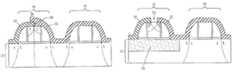
- the present inventionprovides a method and semiconductor structure that overcomes the dual stress liner boundary problem, without significantly increasing the overall size of the integrated circuit. This is achieved in the present invention by ensuring that the dual stress liner boundary between tensile and compressive stress liners is forced to land on a neighboring dummy gate region. By forcing the dual stress liner boundary to land on the dummy gate region, the large stresses associated with the dual stress liner boundary are transferred to the dummy gate region, not directly to the semiconductor substrate. Thus, the impact of the dual stress liner boundary on the nearest neighboring FET is reduced. Additionally, benefits of device variability and packing density are achieved utilizing the present invention.
Landscapes
- Metal-Oxide And Bipolar Metal-Oxide Semiconductor Integrated Circuits (AREA)
- Insulated Gate Type Field-Effect Transistor (AREA)
- Formation Of Insulating Films (AREA)
- Thin Film Transistor (AREA)
Abstract
Description
Claims (1)
Priority Applications (5)
| Application Number | Priority Date | Filing Date | Title |
|---|---|---|---|
| US11/468,402US7462522B2 (en) | 2006-08-30 | 2006-08-30 | Method and structure for improving device performance variation in dual stress liner technology |
| JP2009526029AJP5220749B2 (en) | 2006-08-30 | 2007-08-09 | Method and structure for improving device performance variability in dual stress liner technology |
| PCT/EP2007/058273WO2008025661A1 (en) | 2006-08-30 | 2007-08-09 | Method and structure for improving device performance variation in dual stress liner technology |
| TW096131630ATW200830552A (en) | 2006-08-30 | 2007-08-27 | Method and structure for improving device performance variation in dual stress liner technology |
| US12/328,358US7843024B2 (en) | 2006-08-30 | 2008-12-04 | Method and structure for improving device performance variation in dual stress liner technology |
Applications Claiming Priority (1)
| Application Number | Priority Date | Filing Date | Title |
|---|---|---|---|
| US11/468,402US7462522B2 (en) | 2006-08-30 | 2006-08-30 | Method and structure for improving device performance variation in dual stress liner technology |
Related Child Applications (1)
| Application Number | Title | Priority Date | Filing Date |
|---|---|---|---|
| US12/328,358ContinuationUS7843024B2 (en) | 2006-08-30 | 2008-12-04 | Method and structure for improving device performance variation in dual stress liner technology |
Publications (2)
| Publication Number | Publication Date |
|---|---|
| US20080057653A1 US20080057653A1 (en) | 2008-03-06 |
| US7462522B2true US7462522B2 (en) | 2008-12-09 |
Family
ID=38669778
Family Applications (2)
| Application Number | Title | Priority Date | Filing Date |
|---|---|---|---|
| US11/468,402Expired - Fee RelatedUS7462522B2 (en) | 2006-08-30 | 2006-08-30 | Method and structure for improving device performance variation in dual stress liner technology |
| US12/328,358Active2027-02-11US7843024B2 (en) | 2006-08-30 | 2008-12-04 | Method and structure for improving device performance variation in dual stress liner technology |
Family Applications After (1)
| Application Number | Title | Priority Date | Filing Date |
|---|---|---|---|
| US12/328,358Active2027-02-11US7843024B2 (en) | 2006-08-30 | 2008-12-04 | Method and structure for improving device performance variation in dual stress liner technology |
Country Status (4)
| Country | Link |
|---|---|
| US (2) | US7462522B2 (en) |
| JP (1) | JP5220749B2 (en) |
| TW (1) | TW200830552A (en) |
| WO (1) | WO2008025661A1 (en) |
Cited By (4)
| Publication number | Priority date | Publication date | Assignee | Title |
|---|---|---|---|---|
| US20080102571A1 (en)* | 2006-10-25 | 2008-05-01 | James Pan | Methods for fabricating a stress enhanced mos transistor |
| US7843024B2 (en)* | 2006-08-30 | 2010-11-30 | International Business Machines Corporation | Method and structure for improving device performance variation in dual stress liner technology |
| US20120018803A1 (en)* | 2008-12-19 | 2012-01-26 | Grebs Thomas E | Lateral drain mosfet with substrate drain connection |
| US8436336B2 (en) | 2001-06-18 | 2013-05-07 | Massachusetts Institute Of Technology | Structure and method for a high-speed semiconductor device having a Ge channel layer |
Families Citing this family (14)
| Publication number | Priority date | Publication date | Assignee | Title |
|---|---|---|---|---|
| AU2003238963A1 (en)* | 2002-06-07 | 2003-12-22 | Amberwave Systems Corporation | Semiconductor devices having strained dual channel layers |
| KR100825809B1 (en)* | 2007-02-27 | 2008-04-29 | 삼성전자주식회사 | Structure of semiconductor device having strain layer and manufacturing method thereof |
| US7761838B2 (en)* | 2007-09-26 | 2010-07-20 | Globalfoundries Inc. | Method for fabricating a semiconductor device having an extended stress liner |
| US7932563B2 (en)* | 2009-01-30 | 2011-04-26 | Xilinx, Inc. | Techniques for improving transistor-to-transistor stress uniformity |
| US8638594B1 (en)* | 2009-12-02 | 2014-01-28 | Altera Corporation | Integrated circuits with asymmetric transistors |
| US8467233B2 (en)* | 2011-06-06 | 2013-06-18 | Texas Instruments Incorporated | Asymmetric static random access memory cell with dual stress liner |
| US8466513B2 (en) | 2011-06-13 | 2013-06-18 | Semiconductor Components Industries, Llc | Semiconductor device with enhanced mobility and method |
| CN102891109B (en)* | 2011-07-18 | 2015-04-01 | 中芯国际集成电路制造(上海)有限公司 | Semiconductor device forming method |
| US8779838B2 (en) | 2011-10-25 | 2014-07-15 | International Business Machines Corporation | Methodology and apparatus for tuning driving current of semiconductor transistors |
| US8492218B1 (en) | 2012-04-03 | 2013-07-23 | International Business Machines Corporation | Removal of an overlap of dual stress liners |
| US8778764B2 (en) | 2012-07-16 | 2014-07-15 | Semiconductor Components Industries, Llc | Method of making an insulated gate semiconductor device having a shield electrode structure and structure therefor |
| US9209174B2 (en)* | 2013-02-15 | 2015-12-08 | Globalfoundries Inc. | Circuit element including a layer of a stress-creating material providing a variable stress and method for the formation thereof |
| US9269779B2 (en) | 2014-07-21 | 2016-02-23 | Semiconductor Components Industries, Llc | Insulated gate semiconductor device having a shield electrode structure |
| KR102320820B1 (en) | 2015-02-24 | 2021-11-02 | 삼성전자주식회사 | Integrated circuit device and method of manufacturing the same |
Citations (107)
| Publication number | Priority date | Publication date | Assignee | Title |
|---|---|---|---|---|
| US3602841A (en) | 1970-06-18 | 1971-08-31 | Ibm | High frequency bulk semiconductor amplifiers and oscillators |
| US4665415A (en) | 1985-04-24 | 1987-05-12 | International Business Machines Corporation | Semiconductor device with hole conduction via strained lattice |
| JPS6476755A (en) | 1987-09-18 | 1989-03-22 | Hitachi Ltd | Semiconductor device |
| US4853076A (en) | 1983-12-29 | 1989-08-01 | Massachusetts Institute Of Technology | Semiconductor thin films |
| US4855245A (en) | 1985-09-13 | 1989-08-08 | Siemens Aktiengesellschaft | Method of manufacturing integrated circuit containing bipolar and complementary MOS transistors on a common substrate |
| US4952524A (en) | 1989-05-05 | 1990-08-28 | At&T Bell Laboratories | Semiconductor device manufacture including trench formation |
| US4958213A (en) | 1987-12-07 | 1990-09-18 | Texas Instruments Incorporated | Method for forming a transistor base region under thick oxide |
| US5006913A (en) | 1988-11-05 | 1991-04-09 | Mitsubishi Denki Kabushiki Kaisha | Stacked type semiconductor device |
| US5060030A (en) | 1990-07-18 | 1991-10-22 | Raytheon Company | Pseudomorphic HEMT having strained compensation layer |
| US5081513A (en) | 1991-02-28 | 1992-01-14 | Xerox Corporation | Electronic device with recovery layer proximate to active layer |
| US5108843A (en) | 1988-11-30 | 1992-04-28 | Ricoh Company, Ltd. | Thin film semiconductor and process for producing the same |
| US5134085A (en) | 1991-11-21 | 1992-07-28 | Micron Technology, Inc. | Reduced-mask, split-polysilicon CMOS process, incorporating stacked-capacitor cells, for fabricating multi-megabit dynamic random access memories |
| US5310446A (en) | 1990-01-10 | 1994-05-10 | Ricoh Company, Ltd. | Method for producing semiconductor film |
| US5354695A (en) | 1992-04-08 | 1994-10-11 | Leedy Glenn J | Membrane dielectric isolation IC fabrication |
| US5371399A (en) | 1991-06-14 | 1994-12-06 | International Business Machines Corporation | Compound semiconductor having metallic inclusions and devices fabricated therefrom |
| US5391510A (en) | 1992-02-28 | 1995-02-21 | International Business Machines Corporation | Formation of self-aligned metal gate FETs using a benignant removable gate material during high temperature steps |
| US5459346A (en) | 1988-06-28 | 1995-10-17 | Ricoh Co., Ltd. | Semiconductor substrate with electrical contact in groove |
| US5557122A (en) | 1995-05-12 | 1996-09-17 | Alliance Semiconductors Corporation | Semiconductor electrode having improved grain structure and oxide growth properties |
| US5561302A (en) | 1994-09-26 | 1996-10-01 | Motorola, Inc. | Enhanced mobility MOSFET device and method |
| US5670798A (en) | 1995-03-29 | 1997-09-23 | North Carolina State University | Integrated heterostructures of Group III-V nitride semiconductor materials including epitaxial ohmic contact non-nitride buffer layer and methods of fabricating same |
| US5679965A (en) | 1995-03-29 | 1997-10-21 | North Carolina State University | Integrated heterostructures of Group III-V nitride semiconductor materials including epitaxial ohmic contact, non-nitride buffer layer and methods of fabricating same |
| US5861651A (en) | 1997-02-28 | 1999-01-19 | Lucent Technologies Inc. | Field effect devices and capacitors with improved thin film dielectrics and method for making same |
| US5880040A (en) | 1996-04-15 | 1999-03-09 | Macronix International Co., Ltd. | Gate dielectric based on oxynitride grown in N2 O and annealed in NO |
| US5940716A (en) | 1996-03-15 | 1999-08-17 | Samsung Electronics Co., Ltd. | Methods of forming trench isolation regions using repatterned trench masks |
| US5940736A (en) | 1997-03-11 | 1999-08-17 | Lucent Technologies Inc. | Method for forming a high quality ultrathin gate oxide layer |
| US5960297A (en) | 1997-07-02 | 1999-09-28 | Kabushiki Kaisha Toshiba | Shallow trench isolation structure and method of forming the same |
| US5989978A (en) | 1998-07-16 | 1999-11-23 | Chartered Semiconductor Manufacturing, Ltd. | Shallow trench isolation of MOSFETS with reduced corner parasitic currents |
| US6008126A (en) | 1992-04-08 | 1999-12-28 | Elm Technology Corporation | Membrane dielectric isolation IC fabrication |
| US6025280A (en) | 1997-04-28 | 2000-02-15 | Lucent Technologies Inc. | Use of SiD4 for deposition of ultra thin and controllable oxides |
| US6066545A (en) | 1997-12-09 | 2000-05-23 | Texas Instruments Incorporated | Birdsbeak encroachment using combination of wet and dry etch for isolation nitride |
| US6090684A (en) | 1998-07-31 | 2000-07-18 | Hitachi, Ltd. | Method for manufacturing semiconductor device |
| US6107143A (en) | 1998-03-02 | 2000-08-22 | Samsung Electronics Co., Ltd. | Method for forming a trench isolation structure in an integrated circuit |
| US6117722A (en) | 1999-02-18 | 2000-09-12 | Taiwan Semiconductor Manufacturing Company | SRAM layout for relaxing mechanical stress in shallow trench isolation technology and method of manufacture thereof |
| US6133071A (en) | 1997-10-15 | 2000-10-17 | Nec Corporation | Semiconductor device with plate heat sink free from cracks due to thermal stress and process for assembling it with package |
| US6165383A (en) | 1998-04-10 | 2000-12-26 | Organic Display Technology | Useful precursors for organic electroluminescent materials and devices made from such materials |
| US6221735B1 (en) | 2000-02-15 | 2001-04-24 | Philips Semiconductors, Inc. | Method for eliminating stress induced dislocations in CMOS devices |
| US6228694B1 (en) | 1999-06-28 | 2001-05-08 | Intel Corporation | Method of increasing the mobility of MOS transistors by use of localized stress regions |
| US20010004122A1 (en) | 1999-12-13 | 2001-06-21 | Nec Corporation | Semiconductor device having dummy gates and its manufacturing method |
| US6255169B1 (en) | 1999-02-22 | 2001-07-03 | Advanced Micro Devices, Inc. | Process for fabricating a high-endurance non-volatile memory device |
| US6261964B1 (en) | 1997-03-14 | 2001-07-17 | Micron Technology, Inc. | Material removal method for forming a structure |
| US6265317B1 (en) | 2001-01-09 | 2001-07-24 | Taiwan Semiconductor Manufacturing Company | Top corner rounding for shallow trench isolation |
| US20010009784A1 (en) | 1998-01-09 | 2001-07-26 | Yanjun Ma | Structure and method of making a sub-micron MOS transistor |
| US6274444B1 (en) | 1999-07-30 | 2001-08-14 | United Microelectronics Corp. | Method for forming mosfet |
| US6281532B1 (en) | 1999-06-28 | 2001-08-28 | Intel Corporation | Technique to obtain increased channel mobilities in NMOS transistors by gate electrode engineering |
| US6284626B1 (en) | 1999-04-06 | 2001-09-04 | Vantis Corporation | Angled nitrogen ion implantation for minimizing mechanical stress on side walls of an isolation trench |
| US6284623B1 (en) | 1999-10-25 | 2001-09-04 | Peng-Fei Zhang | Method of fabricating semiconductor devices using shallow trench isolation with reduced narrow channel effect |
| US6319794B1 (en) | 1998-10-14 | 2001-11-20 | International Business Machines Corporation | Structure and method for producing low leakage isolation devices |
| US6361885B1 (en) | 1998-04-10 | 2002-03-26 | Organic Display Technology | Organic electroluminescent materials and device made from such materials |
| US6362082B1 (en) | 1999-06-28 | 2002-03-26 | Intel Corporation | Methodology for control of short channel effects in MOS transistors |
| US6368931B1 (en) | 2000-03-27 | 2002-04-09 | Intel Corporation | Thin tensile layers in shallow trench isolation and method of making same |
| US20020063292A1 (en) | 2000-11-29 | 2002-05-30 | Mark Armstrong | CMOS fabrication process utilizing special transistor orientation |
| US6403486B1 (en) | 2001-04-30 | 2002-06-11 | Taiwan Semiconductor Manufacturing Company | Method for forming a shallow trench isolation |
| US6403975B1 (en) | 1996-04-09 | 2002-06-11 | Max-Planck Gesellschaft Zur Forderung Der Wissenschafteneev | Semiconductor components, in particular photodetectors, light emitting diodes, optical modulators and waveguides with multilayer structures grown on silicon substrates |
| US6406973B1 (en) | 1999-06-29 | 2002-06-18 | Hyundai Electronics Industries Co., Ltd. | Transistor in a semiconductor device and method of manufacturing the same |
| US20020086472A1 (en) | 2000-12-29 | 2002-07-04 | Brian Roberds | Technique to obtain high mobility channels in MOS transistors by forming a strain layer on an underside of a channel |
| US20020086497A1 (en) | 2000-12-30 | 2002-07-04 | Kwok Siang Ping | Beaker shape trench with nitride pull-back for STI |
| US20020090791A1 (en) | 1999-06-28 | 2002-07-11 | Brian S. Doyle | Method for reduced capacitance interconnect system using gaseous implants into the ild |
| US6461936B1 (en) | 2002-01-04 | 2002-10-08 | Infineon Technologies Ag | Double pullback method of filling an isolation trench |
| US6476462B2 (en) | 1999-12-28 | 2002-11-05 | Texas Instruments Incorporated | MOS-type semiconductor device and method for making same |
| US6483171B1 (en) | 1999-08-13 | 2002-11-19 | Micron Technology, Inc. | Vertical sub-micron CMOS transistors on (110), (111), (311), (511), and higher order surfaces of bulk, SOI and thin film structures and method of forming same |
| US6493497B1 (en) | 2000-09-26 | 2002-12-10 | Motorola, Inc. | Electro-optic structure and process for fabricating same |
| US6498358B1 (en) | 2001-07-20 | 2002-12-24 | Motorola, Inc. | Structure and method for fabricating an electro-optic system having an electrochromic diffraction grating |
| US6501121B1 (en) | 2000-11-15 | 2002-12-31 | Motorola, Inc. | Semiconductor structure |
| US6506652B2 (en) | 1998-11-13 | 2003-01-14 | Intel Corporation | Method of recessing spacers to improved salicide resistance on polysilicon gates |
| US20030013259A1 (en) | 2001-07-13 | 2003-01-16 | International Business Machines Corporation | Reduction of polysilicon stress in trench capacitors |
| US20030032261A1 (en) | 2001-08-08 | 2003-02-13 | Ling-Yen Yeh | Method of preventing threshold voltage of MOS transistor from being decreased by shallow trench isolation formation |
| US20030040158A1 (en) | 2001-08-21 | 2003-02-27 | Nec Corporation | Semiconductor device and method of fabricating the same |
| US6531369B1 (en) | 2000-03-01 | 2003-03-11 | Applied Micro Circuits Corporation | Heterojunction bipolar transistor (HBT) fabrication using a selectively deposited silicon germanium (SiGe) |
| US6531740B2 (en) | 2001-07-17 | 2003-03-11 | Motorola, Inc. | Integrated impedance matching and stability network |
| US20030057184A1 (en) | 2001-09-22 | 2003-03-27 | Shiuh-Sheng Yu | Method for pull back SiN to increase rounding effect in a shallow trench isolation process |
| US20030067035A1 (en) | 2001-09-28 | 2003-04-10 | Helmut Tews | Gate processing method with reduced gate oxide corner and edge thinning |
| US6621392B1 (en) | 2002-04-25 | 2003-09-16 | International Business Machines Corporation | Micro electromechanical switch having self-aligned spacers |
| US6635506B2 (en) | 2001-11-07 | 2003-10-21 | International Business Machines Corporation | Method of fabricating micro-electromechanical switches on CMOS compatible substrates |
| US20040029323A1 (en)* | 2000-11-22 | 2004-02-12 | Akihiro Shimizu | Semiconductor device and method for fabricating the same |
| US6717216B1 (en) | 2002-12-12 | 2004-04-06 | International Business Machines Corporation | SOI based field effect transistor having a compressive film in undercut area under the channel and a method of making the device |
| US20040113217A1 (en) | 2002-12-12 | 2004-06-17 | International Business Machines Corporation | Stress inducing spacers |
| US20040113174A1 (en) | 2002-12-12 | 2004-06-17 | International Business Machines Corporation | Isolation structures for imposing stress patterns |
| US20040238914A1 (en) | 2003-05-30 | 2004-12-02 | International Business Machines Corporation | STI stress modification by nitrogen plasma treatment for improving performance in small width devices |
| US6831292B2 (en) | 2001-09-21 | 2004-12-14 | Amberwave Systems Corporation | Semiconductor structures employing strained material layers with defined impurity gradients and methods for fabricating same |
| US20040262784A1 (en) | 2003-06-30 | 2004-12-30 | International Business Machines Corporation | High performance cmos device structures and method of manufacture |
| US20050054148A1 (en) | 2003-09-10 | 2005-03-10 | International Business Machines Corporation | METHOD AND STRUCTURE FOR IMPROVED MOSFETs USING POLY/SILICIDE GATE HEIGHT CONTROL |
| US20050059201A1 (en) | 2003-09-12 | 2005-03-17 | International Business Machines Corporation | Mosfet performance improvement using deformation in soi structure |
| US6869866B1 (en) | 2003-09-22 | 2005-03-22 | International Business Machines Corporation | Silicide proximity structures for CMOS device performance improvements |
| US20050064646A1 (en) | 2003-09-23 | 2005-03-24 | Dureseti Chidambarrao | NFETs using gate induced stress modulation |
| US20050082634A1 (en) | 2003-10-16 | 2005-04-21 | International Business Machines Corporation | High performance strained cmos devices |
| US20050085022A1 (en) | 2003-10-20 | 2005-04-21 | Dureseti Chidambarrao | Strained dislocation-free channels for CMOS and method of manufacture |
| US20050082616A1 (en) | 2003-10-20 | 2005-04-21 | Huajie Chen | High performance stress-enhanced MOSFETs using Si:C and SiGe epitaxial source/drain and method of manufacture |
| US20050093059A1 (en) | 2003-10-30 | 2005-05-05 | Belyansky Michael P. | Structure and method to improve channel mobility by gate electrode stress modification |
| US20050093030A1 (en) | 2003-10-30 | 2005-05-05 | Doris Bruce B. | Structure and method to enhance both nFET and pFET performance using different kinds of stressed layers |
| US20050098829A1 (en) | 2003-11-06 | 2005-05-12 | Doris Bruce B. | High mobility CMOS circuits |
| US20050104131A1 (en) | 2003-11-19 | 2005-05-19 | Dureseti Chidambarrao | Silicon device on Si:C-OI and SGOI and method of manufacture |
| US20050106799A1 (en) | 2003-11-14 | 2005-05-19 | International Business Machines Corporation | Stressed semiconductor device structures having granular semiconductor material |
| US20050130358A1 (en) | 2003-12-12 | 2005-06-16 | Dureseti Chidambarrao | Strained finFETs and method of manufacture |
| US20050145954A1 (en) | 2004-01-05 | 2005-07-07 | International Business Machines Corporation | Structures and methods for making strained mosfets |
| US20050194699A1 (en) | 2004-03-03 | 2005-09-08 | International Business Machines Corporation | Mobility enhanced cmos devices |
| US20050236668A1 (en) | 2004-04-23 | 2005-10-27 | International Business Machines Corporation | STRUCTURES AND METHODS FOR MANUFACTURING OF DISLOCATION FREE STRESSED CHANNELS IN BULK SILICON AND SOI CMOS DEVICES BY GATE STRESS ENGINEERING WITH SiGe AND/OR Si:C |
| US20050258515A1 (en) | 2004-05-21 | 2005-11-24 | International Business Machines Corporation | Embedded stressed nitride liners for CMOS performance improvement |
| US20050260808A1 (en) | 2004-05-21 | 2005-11-24 | International Business Machines Corporation | MOSFET structure with high mechanical stress in the channel |
| US20050269561A1 (en) | 2004-06-03 | 2005-12-08 | Dureseti Chidambarrao | Strained Si on multiple materials for bulk or SOI substrates |
| US20050285137A1 (en) | 2004-06-29 | 2005-12-29 | Fujitsu Limited | Semiconductor device with strain |
| US20060046400A1 (en) | 2004-08-31 | 2006-03-02 | Gert Burbach | Method of forming a semiconductor structure comprising transistor elements with differently stressed channel regions |
| US20060057787A1 (en) | 2002-11-25 | 2006-03-16 | Doris Bruce B | Strained finfet cmos device structures |
| US20060060925A1 (en) | 2004-09-17 | 2006-03-23 | International Business Machines Corporation | Semiconductor device structure with active regions having different surface directions and methods |
| US20060094193A1 (en) | 2004-10-29 | 2006-05-04 | Manfred Horstmann | Semiconductor device including semiconductor regions having differently strained channel regions and a method of manufacturing the same |
| US7052946B2 (en)* | 2004-03-10 | 2006-05-30 | Taiwan Semiconductor Manufacturing Co. Ltd. | Method for selectively stressing MOSFETs to improve charge carrier mobility |
| US20070246741A1 (en)* | 2006-04-24 | 2007-10-25 | Toshiba America Electronic Components, Inc. | Stress relaxation for top of transistor gate |
| US20070252230A1 (en) | 2006-04-28 | 2007-11-01 | International Business Machines Corporation | Cmos structures and methods for improving yield |
Family Cites Families (5)
| Publication number | Priority date | Publication date | Assignee | Title |
|---|---|---|---|---|
| JP2004014954A (en)* | 2002-06-11 | 2004-01-15 | Hitachi Ltd | Semiconductor device |
| JP5002891B2 (en)* | 2004-12-17 | 2012-08-15 | 富士通セミコンダクター株式会社 | Manufacturing method of semiconductor device |
| JP4760414B2 (en)* | 2006-02-06 | 2011-08-31 | ソニー株式会社 | Manufacturing method of semiconductor device |
| US7585720B2 (en)* | 2006-07-05 | 2009-09-08 | Toshiba America Electronic Components, Inc. | Dual stress liner device and method |
| US7462522B2 (en)* | 2006-08-30 | 2008-12-09 | International Business Machines Corporation | Method and structure for improving device performance variation in dual stress liner technology |
- 2006
- 2006-08-30USUS11/468,402patent/US7462522B2/ennot_activeExpired - Fee Related
- 2007
- 2007-08-09JPJP2009526029Apatent/JP5220749B2/ennot_activeExpired - Fee Related
- 2007-08-09WOPCT/EP2007/058273patent/WO2008025661A1/enactiveApplication Filing
- 2007-08-27TWTW096131630Apatent/TW200830552A/enunknown
- 2008
- 2008-12-04USUS12/328,358patent/US7843024B2/enactiveActive
Patent Citations (139)
| Publication number | Priority date | Publication date | Assignee | Title |
|---|---|---|---|---|
| US3602841A (en) | 1970-06-18 | 1971-08-31 | Ibm | High frequency bulk semiconductor amplifiers and oscillators |
| US4853076A (en) | 1983-12-29 | 1989-08-01 | Massachusetts Institute Of Technology | Semiconductor thin films |
| US4665415A (en) | 1985-04-24 | 1987-05-12 | International Business Machines Corporation | Semiconductor device with hole conduction via strained lattice |
| US4855245A (en) | 1985-09-13 | 1989-08-08 | Siemens Aktiengesellschaft | Method of manufacturing integrated circuit containing bipolar and complementary MOS transistors on a common substrate |
| JPS6476755A (en) | 1987-09-18 | 1989-03-22 | Hitachi Ltd | Semiconductor device |
| US4958213A (en) | 1987-12-07 | 1990-09-18 | Texas Instruments Incorporated | Method for forming a transistor base region under thick oxide |
| US5565697A (en) | 1988-06-28 | 1996-10-15 | Ricoh Company, Ltd. | Semiconductor structure having island forming grooves |
| US5459346A (en) | 1988-06-28 | 1995-10-17 | Ricoh Co., Ltd. | Semiconductor substrate with electrical contact in groove |
| US5006913A (en) | 1988-11-05 | 1991-04-09 | Mitsubishi Denki Kabushiki Kaisha | Stacked type semiconductor device |
| US5108843A (en) | 1988-11-30 | 1992-04-28 | Ricoh Company, Ltd. | Thin film semiconductor and process for producing the same |
| US4952524A (en) | 1989-05-05 | 1990-08-28 | At&T Bell Laboratories | Semiconductor device manufacture including trench formation |
| US5310446A (en) | 1990-01-10 | 1994-05-10 | Ricoh Company, Ltd. | Method for producing semiconductor film |
| US5060030A (en) | 1990-07-18 | 1991-10-22 | Raytheon Company | Pseudomorphic HEMT having strained compensation layer |
| US5081513A (en) | 1991-02-28 | 1992-01-14 | Xerox Corporation | Electronic device with recovery layer proximate to active layer |
| US5371399A (en) | 1991-06-14 | 1994-12-06 | International Business Machines Corporation | Compound semiconductor having metallic inclusions and devices fabricated therefrom |
| US5471948A (en) | 1991-06-14 | 1995-12-05 | International Business Machines Corporation | Method of making a compound semiconductor having metallic inclusions |
| US5134085A (en) | 1991-11-21 | 1992-07-28 | Micron Technology, Inc. | Reduced-mask, split-polysilicon CMOS process, incorporating stacked-capacitor cells, for fabricating multi-megabit dynamic random access memories |
| US5391510A (en) | 1992-02-28 | 1995-02-21 | International Business Machines Corporation | Formation of self-aligned metal gate FETs using a benignant removable gate material during high temperature steps |
| US5571741A (en) | 1992-04-08 | 1996-11-05 | Leedy; Glenn J. | Membrane dielectric isolation IC fabrication |
| US5354695A (en) | 1992-04-08 | 1994-10-11 | Leedy Glenn J | Membrane dielectric isolation IC fabrication |
| US5946559A (en) | 1992-04-08 | 1999-08-31 | Elm Technology Corporation | Membrane dielectric isolation IC fabrication |
| US5592018A (en) | 1992-04-08 | 1997-01-07 | Leedy; Glenn J. | Membrane dielectric isolation IC fabrication |
| US5592007A (en) | 1992-04-08 | 1997-01-07 | Leedy; Glenn J. | Membrane dielectric isolation transistor fabrication |
| US5840593A (en) | 1992-04-08 | 1998-11-24 | Elm Technology Corporation | Membrane dielectric isolation IC fabrication |
| US6008126A (en) | 1992-04-08 | 1999-12-28 | Elm Technology Corporation | Membrane dielectric isolation IC fabrication |
| US5561302A (en) | 1994-09-26 | 1996-10-01 | Motorola, Inc. | Enhanced mobility MOSFET device and method |
| US5683934A (en) | 1994-09-26 | 1997-11-04 | Motorola, Inc. | Enhanced mobility MOSFET device and method |
| US5670798A (en) | 1995-03-29 | 1997-09-23 | North Carolina State University | Integrated heterostructures of Group III-V nitride semiconductor materials including epitaxial ohmic contact non-nitride buffer layer and methods of fabricating same |
| US5679965A (en) | 1995-03-29 | 1997-10-21 | North Carolina State University | Integrated heterostructures of Group III-V nitride semiconductor materials including epitaxial ohmic contact, non-nitride buffer layer and methods of fabricating same |
| US6046464A (en) | 1995-03-29 | 2000-04-04 | North Carolina State University | Integrated heterostructures of group III-V nitride semiconductor materials including epitaxial ohmic contact comprising multiple quantum well |
| US5557122A (en) | 1995-05-12 | 1996-09-17 | Alliance Semiconductors Corporation | Semiconductor electrode having improved grain structure and oxide growth properties |
| US5940716A (en) | 1996-03-15 | 1999-08-17 | Samsung Electronics Co., Ltd. | Methods of forming trench isolation regions using repatterned trench masks |
| US6403975B1 (en) | 1996-04-09 | 2002-06-11 | Max-Planck Gesellschaft Zur Forderung Der Wissenschafteneev | Semiconductor components, in particular photodetectors, light emitting diodes, optical modulators and waveguides with multilayer structures grown on silicon substrates |
| US5880040A (en) | 1996-04-15 | 1999-03-09 | Macronix International Co., Ltd. | Gate dielectric based on oxynitride grown in N2 O and annealed in NO |
| US5861651A (en) | 1997-02-28 | 1999-01-19 | Lucent Technologies Inc. | Field effect devices and capacitors with improved thin film dielectrics and method for making same |
| US5940736A (en) | 1997-03-11 | 1999-08-17 | Lucent Technologies Inc. | Method for forming a high quality ultrathin gate oxide layer |
| US6246095B1 (en) | 1997-03-11 | 2001-06-12 | Agere Systems Guardian Corp. | System and method for forming a uniform thin gate oxide layer |
| US6261964B1 (en) | 1997-03-14 | 2001-07-17 | Micron Technology, Inc. | Material removal method for forming a structure |
| US6025280A (en) | 1997-04-28 | 2000-02-15 | Lucent Technologies Inc. | Use of SiD4 for deposition of ultra thin and controllable oxides |
| US5960297A (en) | 1997-07-02 | 1999-09-28 | Kabushiki Kaisha Toshiba | Shallow trench isolation structure and method of forming the same |
| US6133071A (en) | 1997-10-15 | 2000-10-17 | Nec Corporation | Semiconductor device with plate heat sink free from cracks due to thermal stress and process for assembling it with package |
| US6066545A (en) | 1997-12-09 | 2000-05-23 | Texas Instruments Incorporated | Birdsbeak encroachment using combination of wet and dry etch for isolation nitride |
| US20010009784A1 (en) | 1998-01-09 | 2001-07-26 | Yanjun Ma | Structure and method of making a sub-micron MOS transistor |
| US6107143A (en) | 1998-03-02 | 2000-08-22 | Samsung Electronics Co., Ltd. | Method for forming a trench isolation structure in an integrated circuit |
| US6361885B1 (en) | 1998-04-10 | 2002-03-26 | Organic Display Technology | Organic electroluminescent materials and device made from such materials |
| US6165383A (en) | 1998-04-10 | 2000-12-26 | Organic Display Technology | Useful precursors for organic electroluminescent materials and devices made from such materials |
| US5989978A (en) | 1998-07-16 | 1999-11-23 | Chartered Semiconductor Manufacturing, Ltd. | Shallow trench isolation of MOSFETS with reduced corner parasitic currents |
| US6090684A (en) | 1998-07-31 | 2000-07-18 | Hitachi, Ltd. | Method for manufacturing semiconductor device |
| US6319794B1 (en) | 1998-10-14 | 2001-11-20 | International Business Machines Corporation | Structure and method for producing low leakage isolation devices |
| US6521964B1 (en) | 1998-11-13 | 2003-02-18 | Intel Corporation | Device having spacers for improved salicide resistance on polysilicon gates |
| US6509618B2 (en) | 1998-11-13 | 2003-01-21 | Intel Corporation | Device having thin first spacers and partially recessed thick second spacers for improved salicide resistance on polysilicon gates |
| US6506652B2 (en) | 1998-11-13 | 2003-01-14 | Intel Corporation | Method of recessing spacers to improved salicide resistance on polysilicon gates |
| US6117722A (en) | 1999-02-18 | 2000-09-12 | Taiwan Semiconductor Manufacturing Company | SRAM layout for relaxing mechanical stress in shallow trench isolation technology and method of manufacture thereof |
| US6255169B1 (en) | 1999-02-22 | 2001-07-03 | Advanced Micro Devices, Inc. | Process for fabricating a high-endurance non-volatile memory device |
| US6284626B1 (en) | 1999-04-06 | 2001-09-04 | Vantis Corporation | Angled nitrogen ion implantation for minimizing mechanical stress on side walls of an isolation trench |
| US6281532B1 (en) | 1999-06-28 | 2001-08-28 | Intel Corporation | Technique to obtain increased channel mobilities in NMOS transistors by gate electrode engineering |
| US20020090791A1 (en) | 1999-06-28 | 2002-07-11 | Brian S. Doyle | Method for reduced capacitance interconnect system using gaseous implants into the ild |
| US6362082B1 (en) | 1999-06-28 | 2002-03-26 | Intel Corporation | Methodology for control of short channel effects in MOS transistors |
| US6228694B1 (en) | 1999-06-28 | 2001-05-08 | Intel Corporation | Method of increasing the mobility of MOS transistors by use of localized stress regions |
| US20020074598A1 (en) | 1999-06-28 | 2002-06-20 | Doyle Brian S. | Methodology for control of short channel effects in MOS transistors |
| US6406973B1 (en) | 1999-06-29 | 2002-06-18 | Hyundai Electronics Industries Co., Ltd. | Transistor in a semiconductor device and method of manufacturing the same |
| US6274444B1 (en) | 1999-07-30 | 2001-08-14 | United Microelectronics Corp. | Method for forming mosfet |
| US6483171B1 (en) | 1999-08-13 | 2002-11-19 | Micron Technology, Inc. | Vertical sub-micron CMOS transistors on (110), (111), (311), (511), and higher order surfaces of bulk, SOI and thin film structures and method of forming same |
| US6284623B1 (en) | 1999-10-25 | 2001-09-04 | Peng-Fei Zhang | Method of fabricating semiconductor devices using shallow trench isolation with reduced narrow channel effect |
| US20010004122A1 (en) | 1999-12-13 | 2001-06-21 | Nec Corporation | Semiconductor device having dummy gates and its manufacturing method |
| US6476462B2 (en) | 1999-12-28 | 2002-11-05 | Texas Instruments Incorporated | MOS-type semiconductor device and method for making same |
| US6221735B1 (en) | 2000-02-15 | 2001-04-24 | Philips Semiconductors, Inc. | Method for eliminating stress induced dislocations in CMOS devices |
| US6531369B1 (en) | 2000-03-01 | 2003-03-11 | Applied Micro Circuits Corporation | Heterojunction bipolar transistor (HBT) fabrication using a selectively deposited silicon germanium (SiGe) |
| US6368931B1 (en) | 2000-03-27 | 2002-04-09 | Intel Corporation | Thin tensile layers in shallow trench isolation and method of making same |
| US6493497B1 (en) | 2000-09-26 | 2002-12-10 | Motorola, Inc. | Electro-optic structure and process for fabricating same |
| US6501121B1 (en) | 2000-11-15 | 2002-12-31 | Motorola, Inc. | Semiconductor structure |
| US20040029323A1 (en)* | 2000-11-22 | 2004-02-12 | Akihiro Shimizu | Semiconductor device and method for fabricating the same |
| US20020063292A1 (en) | 2000-11-29 | 2002-05-30 | Mark Armstrong | CMOS fabrication process utilizing special transistor orientation |
| US20020086472A1 (en) | 2000-12-29 | 2002-07-04 | Brian Roberds | Technique to obtain high mobility channels in MOS transistors by forming a strain layer on an underside of a channel |
| US20020086497A1 (en) | 2000-12-30 | 2002-07-04 | Kwok Siang Ping | Beaker shape trench with nitride pull-back for STI |
| US6265317B1 (en) | 2001-01-09 | 2001-07-24 | Taiwan Semiconductor Manufacturing Company | Top corner rounding for shallow trench isolation |
| US6403486B1 (en) | 2001-04-30 | 2002-06-11 | Taiwan Semiconductor Manufacturing Company | Method for forming a shallow trench isolation |
| US20030201480A1 (en) | 2001-07-13 | 2003-10-30 | Dureseti Chidambarrao | Trench capacitors with reduced polysilicon stress |
| US6653678B2 (en) | 2001-07-13 | 2003-11-25 | International Business Machines Corporation | Reduction of polysilicon stress in trench capacitors |
| US6872620B2 (en) | 2001-07-13 | 2005-03-29 | International Business Machines Corporation | Trench capacitors with reduced polysilicon stress |
| US20030013259A1 (en) | 2001-07-13 | 2003-01-16 | International Business Machines Corporation | Reduction of polysilicon stress in trench capacitors |
| US6531740B2 (en) | 2001-07-17 | 2003-03-11 | Motorola, Inc. | Integrated impedance matching and stability network |
| US6498358B1 (en) | 2001-07-20 | 2002-12-24 | Motorola, Inc. | Structure and method for fabricating an electro-optic system having an electrochromic diffraction grating |
| US20030032261A1 (en) | 2001-08-08 | 2003-02-13 | Ling-Yen Yeh | Method of preventing threshold voltage of MOS transistor from being decreased by shallow trench isolation formation |
| US20030040158A1 (en) | 2001-08-21 | 2003-02-27 | Nec Corporation | Semiconductor device and method of fabricating the same |
| US6831292B2 (en) | 2001-09-21 | 2004-12-14 | Amberwave Systems Corporation | Semiconductor structures employing strained material layers with defined impurity gradients and methods for fabricating same |
| US20030057184A1 (en) | 2001-09-22 | 2003-03-27 | Shiuh-Sheng Yu | Method for pull back SiN to increase rounding effect in a shallow trench isolation process |
| US20030067035A1 (en) | 2001-09-28 | 2003-04-10 | Helmut Tews | Gate processing method with reduced gate oxide corner and edge thinning |
| US6635506B2 (en) | 2001-11-07 | 2003-10-21 | International Business Machines Corporation | Method of fabricating micro-electromechanical switches on CMOS compatible substrates |
| US6461936B1 (en) | 2002-01-04 | 2002-10-08 | Infineon Technologies Ag | Double pullback method of filling an isolation trench |
| US6621392B1 (en) | 2002-04-25 | 2003-09-16 | International Business Machines Corporation | Micro electromechanical switch having self-aligned spacers |
| US20060057787A1 (en) | 2002-11-25 | 2006-03-16 | Doris Bruce B | Strained finfet cmos device structures |
| US6825529B2 (en) | 2002-12-12 | 2004-11-30 | International Business Machines Corporation | Stress inducing spacers |
| US6974981B2 (en) | 2002-12-12 | 2005-12-13 | International Business Machines Corporation | Isolation structures for imposing stress patterns |
| US20040113174A1 (en) | 2002-12-12 | 2004-06-17 | International Business Machines Corporation | Isolation structures for imposing stress patterns |
| US20050280051A1 (en) | 2002-12-12 | 2005-12-22 | Dureseti Chidambarrao | Isolation structures for imposing stress patterns |
| US20050040460A1 (en) | 2002-12-12 | 2005-02-24 | Dureseti Chidambarrao | Stress inducing spacers |
| US6717216B1 (en) | 2002-12-12 | 2004-04-06 | International Business Machines Corporation | SOI based field effect transistor having a compressive film in undercut area under the channel and a method of making the device |
| US20040113217A1 (en) | 2002-12-12 | 2004-06-17 | International Business Machines Corporation | Stress inducing spacers |
| US20040238914A1 (en) | 2003-05-30 | 2004-12-02 | International Business Machines Corporation | STI stress modification by nitrogen plasma treatment for improving performance in small width devices |
| US20040262784A1 (en) | 2003-06-30 | 2004-12-30 | International Business Machines Corporation | High performance cmos device structures and method of manufacture |
| US20050054148A1 (en) | 2003-09-10 | 2005-03-10 | International Business Machines Corporation | METHOD AND STRUCTURE FOR IMPROVED MOSFETs USING POLY/SILICIDE GATE HEIGHT CONTROL |
| US6890808B2 (en) | 2003-09-10 | 2005-05-10 | International Business Machines Corporation | Method and structure for improved MOSFETs using poly/silicide gate height control |
| US20050145950A1 (en) | 2003-09-10 | 2005-07-07 | Dureseti Chidambarrao | Method and structure for improved MOSFETs using poly/silicide gate height control |
| US20050059201A1 (en) | 2003-09-12 | 2005-03-17 | International Business Machines Corporation | Mosfet performance improvement using deformation in soi structure |
| US6887751B2 (en) | 2003-09-12 | 2005-05-03 | International Business Machines Corporation | MOSFET performance improvement using deformation in SOI structure |
| US20050142788A1 (en) | 2003-09-12 | 2005-06-30 | Dureseti Chidambarrao | MOSFET performance improvement using deformation in SOI structure |
| US6869866B1 (en) | 2003-09-22 | 2005-03-22 | International Business Machines Corporation | Silicide proximity structures for CMOS device performance improvements |
| US20050064687A1 (en) | 2003-09-22 | 2005-03-24 | International Business Machines Corporation | Silicide proximity structures for cmos device performance improvements |
| US20050064646A1 (en) | 2003-09-23 | 2005-03-24 | Dureseti Chidambarrao | NFETs using gate induced stress modulation |
| US20050148146A1 (en) | 2003-10-16 | 2005-07-07 | Doris Bruce D. | High performance strained CMOS devices |
| US20050082634A1 (en) | 2003-10-16 | 2005-04-21 | International Business Machines Corporation | High performance strained cmos devices |
| US20050082616A1 (en) | 2003-10-20 | 2005-04-21 | Huajie Chen | High performance stress-enhanced MOSFETs using Si:C and SiGe epitaxial source/drain and method of manufacture |
| US20050139930A1 (en) | 2003-10-20 | 2005-06-30 | Dureseti Chidambarrao | Strained dislocation-free channels for CMOS and method of manufacture |
| US20050085022A1 (en) | 2003-10-20 | 2005-04-21 | Dureseti Chidambarrao | Strained dislocation-free channels for CMOS and method of manufacture |
| US20050093030A1 (en) | 2003-10-30 | 2005-05-05 | Doris Bruce B. | Structure and method to enhance both nFET and pFET performance using different kinds of stressed layers |
| US20050093059A1 (en) | 2003-10-30 | 2005-05-05 | Belyansky Michael P. | Structure and method to improve channel mobility by gate electrode stress modification |
| US20050282325A1 (en) | 2003-10-30 | 2005-12-22 | Belyansky Michael P | Structure and method to improve channel mobility by gate electrode stress modification |
| US20050245017A1 (en) | 2003-10-30 | 2005-11-03 | Belyansky Michael P | Structure and method to improve channel mobility by gate electrode stress modification |
| US6977194B2 (en) | 2003-10-30 | 2005-12-20 | International Business Machines Corporation | Structure and method to improve channel mobility by gate electrode stress modification |
| US20050098829A1 (en) | 2003-11-06 | 2005-05-12 | Doris Bruce B. | High mobility CMOS circuits |
| US7015082B2 (en) | 2003-11-06 | 2006-03-21 | International Business Machines Corporation | High mobility CMOS circuits |
| US20060027868A1 (en) | 2003-11-06 | 2006-02-09 | Ibm Corporation | High mobility CMOS circuits |
| US20050106799A1 (en) | 2003-11-14 | 2005-05-19 | International Business Machines Corporation | Stressed semiconductor device structures having granular semiconductor material |
| US20050104131A1 (en) | 2003-11-19 | 2005-05-19 | Dureseti Chidambarrao | Silicon device on Si:C-OI and SGOI and method of manufacture |
| US20050130358A1 (en) | 2003-12-12 | 2005-06-16 | Dureseti Chidambarrao | Strained finFETs and method of manufacture |
| US20050145954A1 (en) | 2004-01-05 | 2005-07-07 | International Business Machines Corporation | Structures and methods for making strained mosfets |
| US20050194699A1 (en) | 2004-03-03 | 2005-09-08 | International Business Machines Corporation | Mobility enhanced cmos devices |
| US7052946B2 (en)* | 2004-03-10 | 2006-05-30 | Taiwan Semiconductor Manufacturing Co. Ltd. | Method for selectively stressing MOSFETs to improve charge carrier mobility |
| US20050236668A1 (en) | 2004-04-23 | 2005-10-27 | International Business Machines Corporation | STRUCTURES AND METHODS FOR MANUFACTURING OF DISLOCATION FREE STRESSED CHANNELS IN BULK SILICON AND SOI CMOS DEVICES BY GATE STRESS ENGINEERING WITH SiGe AND/OR Si:C |
| US20050260808A1 (en) | 2004-05-21 | 2005-11-24 | International Business Machines Corporation | MOSFET structure with high mechanical stress in the channel |
| US20050258515A1 (en) | 2004-05-21 | 2005-11-24 | International Business Machines Corporation | Embedded stressed nitride liners for CMOS performance improvement |
| US20050269561A1 (en) | 2004-06-03 | 2005-12-08 | Dureseti Chidambarrao | Strained Si on multiple materials for bulk or SOI substrates |
| US20050285137A1 (en) | 2004-06-29 | 2005-12-29 | Fujitsu Limited | Semiconductor device with strain |
| US20060046400A1 (en) | 2004-08-31 | 2006-03-02 | Gert Burbach | Method of forming a semiconductor structure comprising transistor elements with differently stressed channel regions |
| US20060060925A1 (en) | 2004-09-17 | 2006-03-23 | International Business Machines Corporation | Semiconductor device structure with active regions having different surface directions and methods |
| US20060094193A1 (en) | 2004-10-29 | 2006-05-04 | Manfred Horstmann | Semiconductor device including semiconductor regions having differently strained channel regions and a method of manufacturing the same |
| US20070246741A1 (en)* | 2006-04-24 | 2007-10-25 | Toshiba America Electronic Components, Inc. | Stress relaxation for top of transistor gate |
| US20070252230A1 (en) | 2006-04-28 | 2007-11-01 | International Business Machines Corporation | Cmos structures and methods for improving yield |
Non-Patent Citations (26)
| Title |
|---|
| A. Shimizu, et al., "Local Mechanical-Stress Control (LMC): A New Technique for CMOS-Performance Enhancement." International Electron Devices Meeting, IEEE, Mar. 2001. |
| B. Doyle, et al., "Recovery of Hot-Carrier Damage in Reoxidized Nitrided Oxide MOSFETs." IEEE Electron Device Letters, vol. 13, No. 1, Jan. 1992, pp. 38-40. |
| C.J. Huang, et al., "Temperature Dependence and Post-Stress Recovery of Hot Electron Degradation Effects in Bipolar Transistors." IEEE 1991 Bipolar Circuits and Technology Meeting 7.5, pp. 170-173. |
| D.C. Houghton, et al., "Equilibrium Critical Thickness for SI 1-x GEx Strained Layers on (100) Si". Appl. Phys. Lett. 56 (5), Jan. 29, 1990, pp. 460-462. |
| F. Ootsuka, et al., "A Highly Dense, High-Performance 130nm Node CMOS Technology for Large Scale System-on-a-Chip Application." International Electron Devices Meeting, 23.5.1, IEEE, Apr. 2000. |
| G. Zhang, et al., "A New 'Mixed-Mode' Reliability Degradation Mechanism in Advanced Si and SiGe Bipolar Transistors." IEEE Transactions on Electron Devices, vol. 49, No. 12, Dec. 2002, pp. 2151-2156. |
| Gregory Scott, et al., "NMOS Drive Current Reduction Caused by Transistor Layout and Trench Isolation Induced Stress." International Electron Devices Meeting, 34.4.1, IEEE, Sep. 1999. |
| H. Li, et al., "Design of W-Band VCOs with High Output Power for Potential Application in 77 GHz Automotive Radar Systems." 2003 IEEE GaAs Digest, pp. 263-266. |
| H. Wurzer, et al., "Annealing of Degraded npn-Transistors-Mechanisms and Modeling." IEEE Transactions on Electron Devices, vol. 41, No. 4, Apr. 1994, pp. 533-538. |
| H.S. Momose, et al., "Analysis of the Temperature Dependence of Hot-Carrier-Induced Degradation In Bipolar Transistors for BI-CMOS." IEEE Transactions on Electron Devices, vol. 41, No. 6, Jun. 1994, pp. 978-987. |
| H.S. Momose, et al., "Temperature Dependence of Emitter-Base Reverse Stress Degradation and Its Mechanism Analyzed by MOS Structures." Paper 6.2, pp. 140-143. |
| J.C. Bean, et al., "GEx SI 1-x/Si Strained-Layer Superlattice Grown by Molecular Beam Epitaxy". J. Vac. Sci. Technol. A 2(2), Apr.-Jun. 1984, pp. 436-440. |
| J.H. Van Der Merve, "Regular Articles". Journal of Applied Physics, vol. 34, No. 1, Jan. 1963, pp. 117-122. |
| J.W. Matthews, et al., "Defects in Epitaxial Multilayers". Journal of Crystal Growth 27 (1974), pp. 118-125. |
| K. Ota, et al., "Novel Locally Strained Channel Technique for High Performance 55nm CMOS." International Electron Devices Meeting, 2.2.1, IEEE, Feb. 2002. |
| Kern Rim, et al., "Characteristics and Device Design of Sub-100 nm Strained Si N- and PMOSFETs." 2002 Symposium on VLSI Technology Digest of Technical Papers, IEEE, pp. 98-99. |
| Kern Rim, et al., "Transconductance Enhancement in Deep Submicron Strained-Si n-MOSFETs", International Electron Devices Meeting, 26, 8, 1, IEEE, Sep. 1998. |
| M. Khater, et al., "SiGe HBT Technology with Fmax/Ft=350/300 GHs and Gate Delay Below 3.3 ps". 2004 IEEE, 4 pages. |
| Q. Ouyang et al., "Two-Dimensional Bandgap Engineering in a Novel Si/SiGe pMOSFET with Enhanced Device Performance and Scalability". 2000 IEEE, pp. 151-154. |
| R.H.M. Van De Leur, et al., "Critical Thickness for Pseudomorphic Growth of Si/Ge Alloys and Superlattices". J. Appl. Phys. 64 (6), Sep. 15, 1988, pp. 3043-3050. |
| S.R. Sheng, et al., "Degradation and Recovery of SiGe HBTs Following Radiation and Hot-Carrier Stressing." pp. 14-15. |
| Sheraw, C.D. et al., "Dual stress liner enhancement in hybrid orientation technology," VLSI Technology, 2005, Digest of Technical Papers, 2005 Symposium on Kyoto, Japan, Jun. 14-16, 2005, Piscataway, NJ, USA, IEEE, Jun. 14, 2005, pp. 12-13, XP010818152, ISBN: 4-900784-00-1. |
| Shinya Ito, et al., "Mechanical Stress Effect of Etch-Step Nitride and its Impact on Deep Submicron Transistor Design." International Electron Devices Meeting, 10.7.1, IEEE, Apr. 2000. |
| Subramanian S. Iyer, et al., "Heterojunction Bipolar Transistors Using Si-Ge Alloys". IEEE Transactions on Electron Devices, vol. 36, No. 10, Oct. 1989, pp. 2043-2064. |
| Yang, H.S. et al., "Dual stress liner for high performance sub-45nm gate length SOI CMOS manufacturing," Electron Devices Meeting, 2004, IEDM Technical Digest, IEEE International San Francisco, CA, USA Dec. 13-15, 2004, Piscataway, NJ, USA, IEEE, Dec. 13, 2004, pp. 1075-1077, XP010789003, ISBN: 0-7803-8684-1. |
| Z. Yang, et al., "Avalanche Current Induced Hot Carrier Degradation in 200 Gitz SiGe Heterojunction Bipolar Transistors." pp. 1-5. |
Cited By (5)
| Publication number | Priority date | Publication date | Assignee | Title |
|---|---|---|---|---|
| US8436336B2 (en) | 2001-06-18 | 2013-05-07 | Massachusetts Institute Of Technology | Structure and method for a high-speed semiconductor device having a Ge channel layer |
| US7843024B2 (en)* | 2006-08-30 | 2010-11-30 | International Business Machines Corporation | Method and structure for improving device performance variation in dual stress liner technology |
| US20080102571A1 (en)* | 2006-10-25 | 2008-05-01 | James Pan | Methods for fabricating a stress enhanced mos transistor |
| US7601574B2 (en)* | 2006-10-25 | 2009-10-13 | Globalfoundries Inc. | Methods for fabricating a stress enhanced MOS transistor |
| US20120018803A1 (en)* | 2008-12-19 | 2012-01-26 | Grebs Thomas E | Lateral drain mosfet with substrate drain connection |
Also Published As
| Publication number | Publication date |
|---|---|
| TW200830552A (en) | 2008-07-16 |
| WO2008025661A1 (en) | 2008-03-06 |
| JP5220749B2 (en) | 2013-06-26 |
| US7843024B2 (en) | 2010-11-30 |
| US20090079011A1 (en) | 2009-03-26 |
| JP2010502026A (en) | 2010-01-21 |
| US20080057653A1 (en) | 2008-03-06 |
Similar Documents
| Publication | Publication Date | Title |
|---|---|---|
| US7462522B2 (en) | Method and structure for improving device performance variation in dual stress liner technology | |
| US7405436B2 (en) | Stressed field effect transistors on hybrid orientation substrate | |
| US7952151B2 (en) | Semiconductor devices including fin shaped semiconductor regions and stress inducing layers | |
| US7335929B2 (en) | Transistor with a strained region and method of manufacture | |
| US7791144B2 (en) | High performance stress-enhance MOSFET and method of manufacture | |
| US7227205B2 (en) | Strained-silicon CMOS device and method | |
| US9711413B2 (en) | High performance CMOS device design | |
| US20080179636A1 (en) | N-fets with tensilely strained semiconductor channels, and method for fabricating same using buried pseudomorphic layers | |
| US7808081B2 (en) | Strained-silicon CMOS device and method | |
| US7675055B2 (en) | Strained complementary metal oxide semiconductor (CMOS) on rotated wafers and methods thereof | |
| US20080157200A1 (en) | Stress liner surrounded facetless embedded stressor mosfet | |
| US20130285117A1 (en) | CMOS WITH SiGe CHANNEL PFETs AND METHOD OF FABRICATION | |
| US7790540B2 (en) | Structure and method to use low k stress liner to reduce parasitic capacitance | |
| US20090215277A1 (en) | Dual contact etch stop layer process | |
| US7615418B2 (en) | High performance stress-enhance MOSFET and method of manufacture | |
| US7585773B2 (en) | Non-conformal stress liner for enhanced MOSFET performance | |
| US7675118B2 (en) | Semiconductor structure with enhanced performance using a simplified dual stress liner configuration | |
| US7268362B2 (en) | High performance transistors with SiGe strain | |
| US8445965B2 (en) | Strained semiconductor devices and methods of fabricating strained semiconductor devices |
Legal Events
| Date | Code | Title | Description |
|---|---|---|---|
| AS | Assignment | Owner name:INTERNATIONAL BUSINESS MACHINES CORPORATION, NEW Y Free format text:ASSIGNMENT OF ASSIGNORS INTEREST;ASSIGNORS:CHIDAMBARRAO, DURESETI;GREENE, BRIAN J.;REEL/FRAME:018195/0895 Effective date:20060829 | |
| FEPP | Fee payment procedure | Free format text:PAYOR NUMBER ASSIGNED (ORIGINAL EVENT CODE: ASPN); ENTITY STATUS OF PATENT OWNER: LARGE ENTITY | |
| STCF | Information on status: patent grant | Free format text:PATENTED CASE | |
| REMI | Maintenance fee reminder mailed | ||
| FPAY | Fee payment | Year of fee payment:4 | |
| SULP | Surcharge for late payment | ||
| AS | Assignment | Owner name:GLOBALFOUNDRIES U.S. 2 LLC, NEW YORK Free format text:ASSIGNMENT OF ASSIGNORS INTEREST;ASSIGNOR:INTERNATIONAL BUSINESS MACHINES CORPORATION;REEL/FRAME:036550/0001 Effective date:20150629 | |
| AS | Assignment | Owner name:GLOBALFOUNDRIES INC., CAYMAN ISLANDS Free format text:ASSIGNMENT OF ASSIGNORS INTEREST;ASSIGNORS:GLOBALFOUNDRIES U.S. 2 LLC;GLOBALFOUNDRIES U.S. INC.;REEL/FRAME:036779/0001 Effective date:20150910 | |
| FPAY | Fee payment | Year of fee payment:8 | |
| AS | Assignment | Owner name:WILMINGTON TRUST, NATIONAL ASSOCIATION, DELAWARE Free format text:SECURITY AGREEMENT;ASSIGNOR:GLOBALFOUNDRIES INC.;REEL/FRAME:049490/0001 Effective date:20181127 | |
| FEPP | Fee payment procedure | Free format text:MAINTENANCE FEE REMINDER MAILED (ORIGINAL EVENT CODE: REM.); ENTITY STATUS OF PATENT OWNER: LARGE ENTITY | |
| AS | Assignment | Owner name:GLOBALFOUNDRIES INC., CAYMAN ISLANDS Free format text:RELEASE BY SECURED PARTY;ASSIGNOR:WILMINGTON TRUST, NATIONAL ASSOCIATION;REEL/FRAME:054636/0001 Effective date:20201117 | |
| LAPS | Lapse for failure to pay maintenance fees | Free format text:PATENT EXPIRED FOR FAILURE TO PAY MAINTENANCE FEES (ORIGINAL EVENT CODE: EXP.); ENTITY STATUS OF PATENT OWNER: LARGE ENTITY | |
| STCH | Information on status: patent discontinuation | Free format text:PATENT EXPIRED DUE TO NONPAYMENT OF MAINTENANCE FEES UNDER 37 CFR 1.362 | |
| FP | Lapsed due to failure to pay maintenance fee | Effective date:20201209 | |
| AS | Assignment | Owner name:GLOBALFOUNDRIES U.S. INC., NEW YORK Free format text:RELEASE BY SECURED PARTY;ASSIGNOR:WILMINGTON TRUST, NATIONAL ASSOCIATION;REEL/FRAME:056987/0001 Effective date:20201117 |