US7460246B2 - Method and system for sensing light using interferometric elements - Google Patents
Method and system for sensing light using interferometric elementsDownload PDFInfo
- Publication number
- US7460246B2 US7460246B2US11/066,724US6672405AUS7460246B2US 7460246 B2US7460246 B2US 7460246B2US 6672405 AUS6672405 AUS 6672405AUS 7460246 B2US7460246 B2US 7460246B2
- Authority
- US
- United States
- Prior art keywords
- light
- interferometric
- temperature
- sensor
- temperature sensor
- Prior art date
- Legal status (The legal status is an assumption and is not a legal conclusion. Google has not performed a legal analysis and makes no representation as to the accuracy of the status listed.)
- Expired - Fee Related, expires
Links
Images


Classifications
- G—PHYSICS
- G01—MEASURING; TESTING
- G01J—MEASUREMENT OF INTENSITY, VELOCITY, SPECTRAL CONTENT, POLARISATION, PHASE OR PULSE CHARACTERISTICS OF INFRARED, VISIBLE OR ULTRAVIOLET LIGHT; COLORIMETRY; RADIATION PYROMETRY
- G01J1/00—Photometry, e.g. photographic exposure meter
- G—PHYSICS
- G09—EDUCATION; CRYPTOGRAPHY; DISPLAY; ADVERTISING; SEALS
- G09G—ARRANGEMENTS OR CIRCUITS FOR CONTROL OF INDICATING DEVICES USING STATIC MEANS TO PRESENT VARIABLE INFORMATION
- G09G3/00—Control arrangements or circuits, of interest only in connection with visual indicators other than cathode-ray tubes
- G09G3/20—Control arrangements or circuits, of interest only in connection with visual indicators other than cathode-ray tubes for presentation of an assembly of a number of characters, e.g. a page, by composing the assembly by combination of individual elements arranged in a matrix no fixed position being assigned to or needed to be assigned to the individual characters or partial characters
- G09G3/34—Control arrangements or circuits, of interest only in connection with visual indicators other than cathode-ray tubes for presentation of an assembly of a number of characters, e.g. a page, by composing the assembly by combination of individual elements arranged in a matrix no fixed position being assigned to or needed to be assigned to the individual characters or partial characters by control of light from an independent source
- G09G3/3433—Control arrangements or circuits, of interest only in connection with visual indicators other than cathode-ray tubes for presentation of an assembly of a number of characters, e.g. a page, by composing the assembly by combination of individual elements arranged in a matrix no fixed position being assigned to or needed to be assigned to the individual characters or partial characters by control of light from an independent source using light modulating elements actuated by an electric field and being other than liquid crystal devices and electrochromic devices
- G09G3/3466—Control arrangements or circuits, of interest only in connection with visual indicators other than cathode-ray tubes for presentation of an assembly of a number of characters, e.g. a page, by composing the assembly by combination of individual elements arranged in a matrix no fixed position being assigned to or needed to be assigned to the individual characters or partial characters by control of light from an independent source using light modulating elements actuated by an electric field and being other than liquid crystal devices and electrochromic devices based on interferometric effect
- G—PHYSICS
- G01—MEASURING; TESTING
- G01J—MEASUREMENT OF INTENSITY, VELOCITY, SPECTRAL CONTENT, POLARISATION, PHASE OR PULSE CHARACTERISTICS OF INFRARED, VISIBLE OR ULTRAVIOLET LIGHT; COLORIMETRY; RADIATION PYROMETRY
- G01J3/00—Spectrometry; Spectrophotometry; Monochromators; Measuring colours
- G01J3/12—Generating the spectrum; Monochromators
- G01J3/26—Generating the spectrum; Monochromators using multiple reflection, e.g. Fabry-Perot interferometer, variable interference filters
- G—PHYSICS
- G09—EDUCATION; CRYPTOGRAPHY; DISPLAY; ADVERTISING; SEALS
- G09G—ARRANGEMENTS OR CIRCUITS FOR CONTROL OF INDICATING DEVICES USING STATIC MEANS TO PRESENT VARIABLE INFORMATION
- G09G3/00—Control arrangements or circuits, of interest only in connection with visual indicators other than cathode-ray tubes
- G09G3/20—Control arrangements or circuits, of interest only in connection with visual indicators other than cathode-ray tubes for presentation of an assembly of a number of characters, e.g. a page, by composing the assembly by combination of individual elements arranged in a matrix no fixed position being assigned to or needed to be assigned to the individual characters or partial characters
- G09G3/34—Control arrangements or circuits, of interest only in connection with visual indicators other than cathode-ray tubes for presentation of an assembly of a number of characters, e.g. a page, by composing the assembly by combination of individual elements arranged in a matrix no fixed position being assigned to or needed to be assigned to the individual characters or partial characters by control of light from an independent source
- G09G3/3406—Control of illumination source
- G—PHYSICS
- G02—OPTICS
- G02B—OPTICAL ELEMENTS, SYSTEMS OR APPARATUS
- G02B26/00—Optical devices or arrangements for the control of light using movable or deformable optical elements
- G02B26/001—Optical devices or arrangements for the control of light using movable or deformable optical elements based on interference in an adjustable optical cavity
- G—PHYSICS
- G09—EDUCATION; CRYPTOGRAPHY; DISPLAY; ADVERTISING; SEALS
- G09G—ARRANGEMENTS OR CIRCUITS FOR CONTROL OF INDICATING DEVICES USING STATIC MEANS TO PRESENT VARIABLE INFORMATION
- G09G2320/00—Control of display operating conditions
- G09G2320/04—Maintaining the quality of display appearance
- G09G2320/041—Temperature compensation
- G—PHYSICS
- G09—EDUCATION; CRYPTOGRAPHY; DISPLAY; ADVERTISING; SEALS
- G09G—ARRANGEMENTS OR CIRCUITS FOR CONTROL OF INDICATING DEVICES USING STATIC MEANS TO PRESENT VARIABLE INFORMATION
- G09G2320/00—Control of display operating conditions
- G09G2320/06—Adjustment of display parameters
- G09G2320/0626—Adjustment of display parameters for control of overall brightness
- G—PHYSICS
- G09—EDUCATION; CRYPTOGRAPHY; DISPLAY; ADVERTISING; SEALS
- G09G—ARRANGEMENTS OR CIRCUITS FOR CONTROL OF INDICATING DEVICES USING STATIC MEANS TO PRESENT VARIABLE INFORMATION
- G09G2360/00—Aspects of the architecture of display systems
- G09G2360/14—Detecting light within display terminals, e.g. using a single or a plurality of photosensors
- G09G2360/144—Detecting light within display terminals, e.g. using a single or a plurality of photosensors the light being ambient light
Definitions
- the field of the inventionrelates to microelectromechanical systems (MEMS), and more particularly, to electrical connection architectures for arrays of MEMS elements.
- MEMSmicroelectromechanical systems
- Microelectromechanical systemsinclude micromechanical elements, actuators, and electronics. Micromechanical elements may be created using deposition, etching, and or other micromachining processes that etch away parts of substrates and/or deposited material layers or that add layers to form electrical and electromechanical devices.
- MEMS deviceOne type of MEMS device is called an interferometric modulator.
- An interferometric modulatormay comprise a pair of conductive plates, one or both of which may be partially transparent and capable of relative motion upon application of an appropriate electrical signal.
- One platemay comprise a stationary layer deposited on a substrate, the other plate may comprise a metallic membrane suspended over the stationary layer.
- Arrays of independently actuatable interferometric light modulatorsare used in certain display configurations as display elements.
- the light modulatorsare electrically connected so as to provide the control voltages or signals used to individually actuate each light modulator.
- Certain embodiments of the inventionprovide a light sensor comprising at least one interferometric element that absorbs light in at least one wavelength.
- the interferometric elementcomprises a first surface and a second surface substantially parallel to the first surface. The second surface is spaced a gap distance from the first surface in a direction substantially perpendicular to the first surface. The light wavelength absorbed is dependent on the gap distance.
- the interferometric elementfurther comprises a temperature sensor. The temperature sensor is responsive to changes in temperature of at least a portion of the interferometric element due to absorption of light by the interferometric element.
- the light sensorcomprises a plurality of interferometric elements.
- Each interferometric elementhas a corresponding gap distance and absorbs light in at least one wavelength.
- each interferometric elementcomprises substantially the same gap distance as the other interferometric elements.
- the plurality of interferometric elementscomprises two or more subsets of interferometric elements. Each interferometric element of a subset comprises substantially the same gap distance as the other interferometric elements of the subset. Each subset has a different gap distance and absorbs light in at least one different wavelength.
- the light sensorfurther comprises an array of color filters.
- Each color filteris positioned such that light impinging on a corresponding interferometric element propagates through the color filter.
- Each color filtersubstantially transmits at least one wavelength of light that corresponds to the interferometric element.
- the first surface of the interferometric elementis a fixed surface and the second surface is a movable surface.
- the movable surfaceIn a first state of the interferometric element, the movable surface is spaced a first distance from the fixed surface in a direction substantially perpendicular to the fixed surface. In a second state, the movable surface is spaced a second distance, different from the first distance, from the fixed surface in a direction substantially perpendicular to the fixed surface. In certain embodiments, either the first distance or the second distance is approximately zero.
- the interferometric elementcomprises two or more colors. In certain embodiments, the interferometric element comprises a single color of light (e.g., red, green, or blue light).
- At least one interferometric elementis used as a light sensor. In certain other embodiments, a plurality of interferometric elements is used for image capture.
- FIG. 1is an isometric view depicting a portion of one embodiment of an interferometric modulator display in which a movable reflective layer of a first interferometric modulator is in a released position and a movable reflective layer of a second interferometric modulator is in an actuated position.
- FIG. 2is a system block diagram illustrating one embodiment of an electronic device incorporating a 3 ⁇ 3 interferometric modulator display.
- FIG. 3is a diagram of movable mirror position versus applied voltage for one exemplary embodiment of an interferometric modulator of FIG. 1 .
- FIG. 4is an illustration of a set of row and column voltages that may be used to drive an interferometric modulator display.
- FIGS. 5A and 5Billustrate one exemplary timing diagram for row and column signals that may be used to write a frame of display data to the 3 ⁇ 3 interferometric modulator display of FIG. 3 .
- FIG. 6Ais a cross section of the device of FIG. 1 .
- FIG. 6Bis a cross section of an alternative embodiment of an interferometric modulator.
- FIG. 6Cis a cross section of another alternative embodiment of an interferometric modulator.
- FIG. 7schematically illustrates an interferometric element compatible with embodiments described herein.
- FIG. 8schematically illustrates a plurality of interferometric elements, each element having a different gap distance.
- FIG. 9schematically illustrates a plurality of interferometric elements, each having temperatures sensors responsive to different ranges of temperatures.
- FIGS. 10A and 10Bschematically illustrate two embodiments of a light sensor having a plurality of interferometric elements with substantially equal gap distances and a plurality of color filters.
- FIG. 11is a graph of transmittance spectra for a set of three exemplary color filter materials compatible with embodiments described herein.
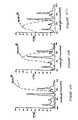
- FIGS. 12A , 12 B, and 12 Care three graphs of the transmittance spectra of the color filter materials of FIG. 11 overlaid with the emission spectrum from a backlight source.
- FIG. 13is a system block diagram illustrating one embodiment of an electronic device incorporating an interferometric element having a temperature sensor for use with a sidelight source.
- FIG. 14is a system block diagram illustrating one embodiment of an electronic device incorporating an interferometric element having a temperature sensor for use with a backlight source.
- FIG. 15illustrates a series of exemplary steps for sensing light by an electronic device having an interferometric element and temperature sensor.
- the interferometric elementabsorbs a wavelength of ambient light in the form of heat on a surface of the interferometric modulator.
- the absorbed heatis sensed by the temperature sensor.
- the temperature sensormay be a contact or non-contact sensor.
- the temperature sensorresponds to the heat absorbed by the surface of the interferometric modulator.
- the temperature sensoroutputs data, for example a voltage, indicative of the sensed temperature.
- the outputted datais processed and stored as a digital image.
- the outputted datais utilized to set the amount of front light or back light illuminating a display device to better make the display device readable in the ambient light.
- the following detailed descriptionis directed to certain specific embodiments of the invention. However, the invention can be embodied in a multitude of different ways. In this description, reference is made to the drawings wherein like parts are designated with like numerals throughout. As will be apparent from the following description, the invention may be implemented in any device that is configured to display an image, whether in motion (e.g., video) or stationary (e.g., still image), and whether textual or pictorial.
- motione.g., video
- stationarye.g., still image
- the inventionmay be implemented in or associated with a variety of electronic devices such as, but not limited to, mobile telephones, wireless devices, personal data assistants (PDAs), hand-held or portable computers, GPS receivers/navigators, cameras, MP3 players, camcorders, game consoles, wrist watches, clocks, calculators, television monitors, flat panel displays, computer monitors, auto displays (e.g., odometer display, etc.), cockpit controls and/or displays, display of camera views (e.g., display of a rear view camera in a vehicle), electronic photographs, electronic billboards or signs, projectors, architectural structures, packaging, and aesthetic structures (e.g., display of images on a piece of jewelry).
- MEMS devices of similar structure to those described hereincan also be used in non-display applications such as in electronic switching devices.
- FIG. 1One interferometric modulator display embodiment comprising an interferometric MEMS display element is illustrated in FIG. 1 .
- the pixelsare in either a bright or dark state.
- the display elementIn the bright (“on” or “open”) state, the display element reflects a large portion of incident visible light to a user.
- the dark (“off” or “closed”) stateWhen in the dark (“off” or “closed”) state, the display element reflects little incident visible light to the user.
- the light reflectance properties of the “on” and “off” statesmay be reversed.
- MEMS pixelscan be configured to reflect predominantly at selected colors, allowing for a color display in addition to black and white.
- FIG. 1is an isometric view depicting two adjacent pixels in a series of pixels of a visual display, wherein each pixel comprises a MEMS interferometric modulator.
- an interferometric modulator displaycomprises a row/column array of these interferometric modulators.
- Each interferometric modulatorincludes a pair of reflective layers positioned at a variable and controllable distance from each other to form a resonant optical cavity with at least one variable dimension.
- one of the reflective layersmay be moved between two positions. In the first position, referred to herein as the released state, the movable layer is positioned at a relatively large distance from a fixed partially reflective layer.
- the movable layerIn the second position, the movable layer is positioned more closely adjacent to the partially reflective layer. Incident light that reflects from the two layers interferes constructively or destructively depending on the position of the movable reflective layer, producing either an overall reflective or non-reflective state for each pixel.
- the depicted portion of the pixel array in FIG. 1includes two adjacent interferometric modulators 12 a and 12 b .
- a movable and highly reflective layer 14 ais illustrated in a released position at a predetermined distance from a fixed partially reflective layer 16 a .
- the movable highly reflective layer 14 bis illustrated in an actuated position adjacent to the fixed partially reflective layer 16 b.
- the fixed layers 16 a , 16 bare electrically conductive, partially transparent and partially reflective, and may be fabricated, for example, by depositing one or more layers each of chromium and indium-tin-oxide onto a transparent substrate 20 .
- the layersare patterned into parallel strips, and may form row electrodes in a display device as described further below.
- the movable layers 14 a , 14 bmay be formed as a series of parallel strips of a deposited metal layer or layers (orthogonal to the row electrodes 16 a , 16 b ) deposited on top of posts 18 and an intervening sacrificial material deposited between the posts 18 .
- the deformable metal layersare separated from the fixed metal layers by a defined air gap 19 .
- a highly conductive and reflective materialsuch as aluminum may be used for the deformable layers, and these strips may form column electrodes in a display device.
- the cavity 19remains between the layers 14 a , 16 a and the deformable layer in a mechanically relaxed state as illustrated by the pixel 12 a in FIG. 1 .
- the capacitor formed at the intersection of the row and column electrodes at the corresponding pixelbecomes charged, and electrostatic forces pull the electrodes together.
- the movable layeris deformed and is forced against the fixed layer (a dielectric material which is not illustrated in this Figure may be deposited on the fixed layer to prevent shorting and control the separation distance) as illustrated by the pixel 12 b on the right in FIG. 1 .
- the behavioris the same regardless of the polarity of the applied potential difference. In this way, row/column actuation that can control the reflective vs. non-reflective pixel states is analogous in many ways to that used in conventional LCD and other display technologies.
- FIGS. 2 through 5illustrate one exemplary process and system for using an array of interferometric modulators in a display application.
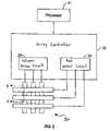
- FIG. 2is a system block diagram illustrating one embodiment of an electronic device that may incorporate aspects of the invention.
- the electronic deviceincludes a processor 21 which may be any general purpose single- or multi-chip microprocessor such as an ARM, Pentium®, Pentium II®, Pentium III®, Pentium IV®, Pentium® Pro, an 8051, a MIPS®, a Power PC®, an ALPHA®, or any special purpose microprocessor such as a digital signal processor, microcontroller, or a programmable gate array.
- the processor 21may be configured to execute one or more software modules.
- the processormay be configured to execute one or more software applications, including a web browser, a telephone application, an email program, or any other software application.
- the processor 21is also configured to communicate with an array controller 22 .
- the array controller 22includes a row driver circuit 24 and a column driver circuit 26 that provide signals to a pixel array 30 .
- the cross section of the array illustrated in FIG. 1is shown by the lines 1 - 1 in FIG. 2 .
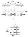
- the row/column actuation protocolmay take advantage of a hysteresis property of these devices illustrated in FIG. 3 . It may require, for example, a 10 volt potential difference to cause a movable layer to deform from the released state to the actuated state. However, when the voltage is reduced from that value, the movable layer maintains its state as the voltage drops back below 10 volts.
- the movable layerdoes not release completely until the voltage drops below 2 volts.
- There is thus a range of voltage, about 3 to 7 V in the example illustrated in FIG. 3where there exists a window of applied voltage within which the device is stable in either the released or actuated state. This is referred to herein as the “hysteresis window” or “stability window.”
- hysteresis windowor “stability window.”
- the row/column actuation protocolcan be designed such that during row strobing, pixels in the strobed row that are to be actuated are exposed to a voltage difference of about 10 volts, and pixels that are to be released are exposed to a voltage difference of close to zero volts. After the strobe, the pixels are exposed to a steady state voltage difference of about 5 volts such that they remain in whatever state the row strobe put them in. After being written, each pixel sees a potential difference within the “stability window” of 3-7 volts in this example. This feature makes the pixel design illustrated in FIG. 1 stable under the same applied voltage conditions in either an actuated or released pre-existing state.
- each pixel of the interferometric modulatoris essentially a capacitor formed by the fixed and moving reflective layers, this stable state can be held at a voltage within the hysteresis window with almost no power dissipation. Essentially no current flows into the pixel if the applied potential is fixed.
- a display framemay be created by asserting the set of column electrodes in accordance with the desired set of actuated pixels in the first row.
- a row pulseis then applied to the row 1 electrode, actuating the pixels corresponding to the asserted column lines.
- the asserted set of column electrodesis then changed to correspond to the desired set of actuated pixels in the second row.
- a pulseis then applied to the row 2 electrode, actuating the appropriate pixels in row 2 in accordance with the asserted column electrodes.
- the row 1 pixelsare unaffected by the row 2 pulse, and remain in the state they were set to during the row 1 pulse. This may be repeated for the entire series of rows in a sequential fashion to produce the frame.
- the framesare refreshed and/or updated with new display data by continually repeating this process at some desired number of frames per second.
- protocols for driving row and column electrodes of pixel arrays to produce display framesare also well known and may be used in conjunction with the present invention.
- FIGS. 4 and 5illustrate one possible actuation protocol for creating a display frame on the 3 ⁇ 3 array of FIG. 2 .
- FIG. 4illustrates a possible set of column and row voltage levels that may be used for pixels exhibiting the hysteresis curves of FIG. 3 .
- actuating a pixelinvolves setting the appropriate column to ⁇ V bias , and the appropriate row to + ⁇ V, which may correspond to ⁇ 5 volts and +5 volts respectively Releasing the pixel is accomplished by setting the appropriate column to +V bias , and the appropriate row to the same + ⁇ V, producing a zero volt potential difference across the pixel. In those rows where the row voltage is held at zero volts, the pixels are stable in whatever state they were originally in, regardless of whether the column is at +V bias , or ⁇ V bias .
- FIG. 5Bis a timing diagram showing a series of row and column signals applied to the 3 ⁇ 3 array of FIG. 2 which will result in the display arrangement illustrated in FIG. 5A , where actuated pixels are non-reflective.
- the pixelsPrior to writing the frame illustrated in FIG. 5A , the pixels can be in any state, and in this example, all the rows are at 0 volts, and all the columns are at +5 volts. With these applied voltages, all pixels are stable in their existing actuated or released states.
- pixels ( 1 , 1 ), ( 1 , 2 ), ( 2 , 2 ), ( 3 , 2 ) and ( 3 , 3 )are actuated.
- columns 1 and 2are set to ⁇ 5 volts
- column 3is set to +5 volts. This does not change the state of any pixels, because all the pixels remain in the 3-7 volt stability window.
- Row 1is then strobed with a pulse that goes from 0, up to 5 volts, and back to zero. This actuates the ( 1 , 1 ) and ( 1 , 2 ) pixels and releases the ( 1 , 3 ) pixel. No other pixels in the array are affected.
- row 2is set to ⁇ 5 volts, and columns 1 and 3 are set to +5 volts.
- the same strobe applied to row 2will then actuate pixel ( 2 , 2 ) and release pixels ( 2 , 1 ) and ( 2 , 3 ). Again, no other pixels of the array are affected.
- Row 3is similarly set by setting columns 2 and 3 to ⁇ 5 volts, and column 1 to +5 volts.
- the row 3strobe sets the row 3 pixels as shown in FIG. 5A . After writing the frame, the row potentials are zero, and the column potentials can remain at either +5 or ⁇ 5 volts, and the display is then stable in the arrangement of FIG. 5A .
- FIGS. 6A-6Cillustrate three different embodiments of the moving mirror structure.
- FIG. 6Ais a cross section of the embodiment of FIG. 1 , where a strip of metal material 14 is deposited on orthogonally extending supports 18 .
- the moveable reflective material 14is attached to supports at the corners only, on tethers 32 .
- the moveable reflective material 14is suspended from a deformable layer 34 .
- This embodimenthas benefits because the structural design and materials used for the reflective material 14 can be optimized with respect to the optical properties, and the structural design and materials used for the deformable layer 34 can be optimized with respect to desired mechanical properties.
- these interferometric elementsprovide the capability to individually address and switch selected interferometric elements between at least two states with different reflection and transmission properties.
- Other interferometric elements which are not switchableare also compatible with embodiments described herein.
- FIG. 7schematically illustrates an interferometric element 700 having a temperature sensor 708 .
- the illustrated embodiment of the interferometric element 700is not switchable and thus does not switch between “off” and “on” states as described above.
- the description of the interferometric element 700applies equally to switchable embodiments including the exemplary switchable embodiments illustrated in FIGS. 6A , 6 B, and 6 C.
- the exemplary switchable embodiments illustrated in FIGS. 6A , 6 B, and 6 Cmay include the temperature sensor 708 .
- the interferometric elementmay switch between “on” and “off” states as well as sense ambient light.
- Embodiments of the exemplary switchable elementsillustrate in FIGS.
- the characteristics sensed by the interferometric elementmay be utilized to control an optical compensation structure.
- the optical compensation structureis a front light, side light, or back light associated with a display electronic device.
- the detected intensity or brightness of ambient lightcan be advantageously used in such embodiments to set the amount of illuminating light for the display electronic device to better make the display device readable in the ambient light.
- the interferometric element 700is configured to sense ambient light.
- the temperature sensor 708provides one or more characteristics of the sensed ambient light to an electronic device. Characteristics of ambient light include, but are not limited to, wavelength and intensity. Exemplary electronic devices include cameras and fingerprint sensors.
- the interferometric element 700senses ambient light having at least one wavelength and an intensity associated with the wavelength.
- a camera devicereceives and stores these characteristics. To form a picture, the camera may receive characteristics from a plurality of adjacent interferometric elements arranged in an array of interferometric elements. In certain embodiments, the received characteristics from the array of interferometric elements are processed and stored as a digital image. Uses of the interferometric element 700 as a camera or other image capture device are described in greater detail in connection with FIG. 8 .
- switchable and non-switchable interferometric elementsare both utilized in a display electronic device.
- On or more of the switchable or non-switchablemay include a temperature sensor 708 .
- the switchable or non-switchable interferometric element having the sensormay be located within or outside of the array of switching interferometric elements.
- the interferometric element 700comprises a first surface 702 and a second surface 704 substantially parallel to the first surface 702 .
- the second surface 704is spaced a gap distance d 0 from the first surface 702 in a direction substantially perpendicular to the first surface 702 .
- the first surface 702is partially transmissive and partially reflective to the at least one wavelength.
- the second surface 704is at least partially reflective to light.
- Exemplary materials for the first surface 702 and the second surface 704include, but are not limited to, chrome or titanium.
- the first surface 702 and the second surface 704form a resonant cavity (e.g., etalon) in which light interferes with itself as it reflects between the first surface 702 and the second surface 704 .
- the interferometric element 700absorbs light having at least one wavelength. The at least one wavelength is dependent on the gap distance d 0 .
- the interferometric element 700further comprises a substrate 706 which is substantially transmissive to the at least one wavelength. Light enters the interferometric element 700 through the substrate 706 and reflects between the first surface 702 and the second surface 704 .
- At least a portion of the light incident on the interferometric element 700 having the at least one wavelengthis absorbed by the interferometric element 700 .
- the energy associated with this absorbed light in the first surface 702is dissipated as heat.
- the first surface 702 of certain embodimentsis on the substrate 706 , as schematically illustrated by FIG. 7
- the interferometric element 700comprises one or more layers (e.g., dielectric layers) that are on the first surface 702 such that the first surface 702 is between these layers and the substrate 706 .
- the interferometric element 700further comprises a temperature sensor 708 .
- the temperature sensor 708is responsive to changes of temperature of at least a portion of the interferometric element 700 from absorption of light by the interferometric element 700 .
- the temperature sensor 708is on the first surface 702 and is between the first surface 702 and the second surface 704 .
- Other positions of the temperature sensor 708are compatible with embodiments described herein.
- the temperature sensor 708is located adjacent to or spaced from the first surface 702 .
- the temperature sensor 708may sense a change in temperature of the portion of the first surface 702 via radiation, convection, conduction, or a combination of one or more physical processes for transferring heat energy.
- the temperature sensor 708may be located near or adjacent to an optical stack.
- the optical stackincludes the fixed layers 16 a , 16 b and layers adjacent to the fixed layers. These adjacent layers may include layers of dielectric, chromium, indium-tin-oxide, and the transparent substrate 20 .
- the absorption and the corresponding heatare functions of wavelength.
- the interferometric element 700can have different absorption coefficients for red light, green light, and blue light, thereby yielding different amounts of heat for these various wavelengths of incident light.
- the materials of the interferometric element 700are selected to provide sensitivity to selected ranges of wavelengths. Ranges of wavelengths which can be detected by interferometric elements 700 compatible with embodiments described herein include, but are not limited to, visible wavelengths, infra-red and ultra-violet wavelengths, radio-frequency (RF) wavelengths, and x-rays.
- RFradio-frequency
- the temperature sensor 708comprises a binary device (e.g., a switch) which is in a first state when the temperature is below a predetermined level and is in a second state when the temperature is above a predetermined level. Certain such switches are formed using micro-electro-mechanical system (MEMS) fabrication techniques. In certain other embodiments, the temperature sensor 708 comprises an analog device.
- a binary devicee.g., a switch
- MEMSmicro-electro-mechanical system
- the temperature sensor 708may be a contact or non-contact sensor.
- Exemplary contact temperature sensorsthat may be used with the embodiments described herein include thermocouples, thermistors, resistance temperature detectors (RTDs), filled system thermometers, bi-metallic thermometers, and semiconductor temperature sensors.
- RTDsresistance temperature detectors
- a bimetallic thermocouplecan be used to generate a voltage difference as a function of the temperature.
- Exemplary non-contact temperature sensorsthat may be used with the embodiments described herein include radiation thermometers (for example, pyrometers), thermal imagers, ratio thermometers, optical pyrometers, and fiber optic temperature sensors.
- Other temperature sensors 708are compatible with embodiments described herein.
- more or less surface area of the temperature sensor 708contacts the first surface 702 .
- Increasing the contact surface area between the temperature sensor 708 and the first surface 702may advantageously increase the sensitivity of the characteristics measured by the temperature sensor 708 .
- the temperature of the interferometric element 700increases, and the temperature sensor 708 responds to the temperature increase.
- the response of the temperature sensor 708is determined by measuring a change in voltage of the temperature sensor 708 .
- the temperature sensor 708measures a voltage (V 0 ⁇ V 1 ). A change in voltage between V 0 and V 1 corresponds to a change in the temperature of the portion of the first surface 702 .
- the temperature sensor 708measures, for example, current, resistance, and/or deflection depending on the selected type of temperature sensor 708 .
- the increase of temperatureis dependent on the intensity of the light at the at least one wavelength absorbed by the interferometric element 700 .
- the interferometric element 700thus serves as a light sensor which is sensitive to the at least one wavelength.
- the size of the interferometric elements 700is a function of the micro-fabrication design rules. In a semiconductor fab, certain embodiments with interferometric elements 700 having areas less than or equal to approximately one square micron are possible. Other certain embodiments provide interferometric elements 700 having areas less than or equal to approximately one-half square micron. Other sizes of interferometric elements 700 are also compatible with embodiments described herein.
- FIG. 8schematically illustrates a plurality of interferometric elements 700 comprising three sets of interferometric elements 700 .
- a first set 800 of interferometric elements 700has a gap distance d 1 which corresponds to being substantially reflective to a first range of wavelengths and at least partially absorptive to other wavelengths.
- a second set 802 of interferometric elements 700has a second gap distance d 2 which corresponds to being substantially reflective to a second range of wavelengths and at least partially absorptive to other wavelengths.
- a third set 804 of interferometric elements 700has a third gap distance d 3 which corresponds to being substantially reflective to a third range of wavelengths and at least partially absorptive to other wavelengths.
- the temperature sensor 708could be made of different materials and/or have a different architecture (MEMS/bi-metallic, etc.) for the three different gaps to optimize their sensitivity.
- each range of wavelengthscomprises a range of colors. In certain embodiments, each range of wavelengths comprises two or more colors. In certain embodiments, the first, second, and third ranges of wavelengths correspond to red, green, and blue, while in other embodiments, the first, second, and third colors correspond to cyan, magenta, and yellow. Certain such embodiments advantageously provide measurements of the intensity of each spectral component. Other ranges of wavelengths are compatible with embodiments described herein.
- certain embodimentsprovide a light sensor which can distinguish between wavelengths.
- a light imaging sensorcan be built.
- Each pixel of the light imaging sensorconsists of the interferometric element 700 that measures the intensity of light for red, green and blue by the respective temperature changes.
- the coloris detected by different temperature increase for the three primaries, red, blue and green.
- Certain such embodimentscan be used for image capture, while certain other embodiments can be used for monitoring the brightness of ambient light.
- the detected brightness of ambient lightcan be advantageously used in certain embodiments to set the amount of front light or back light illuminating a display device to better make the display device readable in the ambient light.
- a CCD camerauses an array of interferometric elements 700 having a temperature sensor 708 instead of a piece of silicon to receive incoming light.
- Each of the interferometric elementssense incoming light as described with reference to FIGS. 6-10 .
- Lightis allowed to impinge on the interferometric sensor until the light is extinguished.
- simple electronic circuitry and a microprocessor or computerare used to unload the interferometric sensor, measure the voltage change in each sensor, and process the resulting data into an image on a video monitor or other output media.
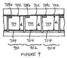
- FIG. 9schematically illustrates a plurality of interferometric elements 700 comprising three sets of interferometric elements 700 .
- Each of the interferometric elements 700has approximately the same gap distance d 0 , so the interferometric elements 700 are absorptive to the same at least one wavelength.
- a first set 900 of interferometric elements 700has a first temperature sensor 708 a which is responsive to a first range of temperatures associated with certain ambient or incident light intensity.
- a second set 902 of interferometric elements 700has a second temperature sensor 708 b which is responsive to a second range of temperatures that is associated with a certain range of ambient or incident light intensity.
- a third set 904 of interferometric elements 700has a third temperature sensor 708 c which is responsive to a third range of temperatures that is associated with a certain range of ambient or incident light intensity. In certain embodiments, one or more of the first range, second range, and third range of temperatures overlap one another.
- certain embodimentsadvantageously provide a more precise determination of the light intensity in the at least one wavelength absorbed by the interferometric element 700 than is achieved by using temperature sensors 708 responsive to a single range of temperatures.
- the first temperature sensor 708 ais a binary device which switches between two states at a first temperature T 1
- the second temperature sensor 708 bis a binary device which switches between two states at a second temperature T 2 higher than T 1
- the third temperature sensor 708 cis a binary device which switches between two states at a third temperature T 3 higher than T 2 .
- certain embodimentscan determine whether the temperature of the interferometric elements 700 is below T 1 , between T 1 and T 2 , between T 2 and T 3 , or above T 3 .
- a single interferometric element 700comprises more than one temperature sensor 708 to provide a similar capability.
- interferometric elements 700which provide the capability to individually address and switch selected interferometric elements 700 between at least two states with different reflection and transmission properties.
- an interferometric element 700can be switched between two or more states to change the range of wavelengths which the interferometric element 700 absorbs.
- certain embodimentsadvantageously provide the capability to modify the response of the interferometric element 700 at will.
- FIGS. 10A and 10Bschematically illustrates exemplary embodiments of a light sensor 1000 comprising an array of interferometric elements 1002 and an array of color filters 1004 .
- Each interferometric element 1002is substantially reflective to at least one wavelength and is at least partially absorptive at other wavelengths.
- each of the interferometric elements 1002has the same gap distance d 0 such that each interferometric element 1002 absorbs the same at least one wavelength as do the other interferometric elements 1002 .
- Each color filter 1004is positioned such that light reflected from a corresponding interferometric element 1002 propagates through the color filter 1004 .
- the color filters 1004are positioned outside an outer surface 1006 of a substrate 1008 of the light sensor 1000 .
- the color filters 1004are positioned within the outer surface 1006 and are integral with the array of interferometric elements 1002 .
- Each color filter 1004has a characteristic transmittance spectrum in which a selected range of wavelengths is substantially transmitted through the color filter 1004 while other wavelengths are substantially not transmitted (e.g., either reflected or absorbed) by the color filter 1004 .
- the array of color filters 1004comprises three subsets of the color filters 1004 .
- Each color filter 1004 of the first subsethas a first transmittance spectrum
- each color filter 1004 of the second subsethas a second transmittance spectrum
- each color filter 1004 of the third subsethas a third transmittance spectrum.
- the first, second, and third subsets of the color filters 1004have transmittance spectra corresponding to substantial transmittance of red, green, and blue light, respectively.
- the first, second, and third subsets of the color filters 1004have transmittance spectra corresponding to substantial transmittance of cyan, magenta, and yellow light, respectively.
- Other color filters 1004 with other transmittance spectraare compatible with embodiments described herein.
- FIG. 11is a graph of the transmittance (T) as a function of wavelength ( ⁇ ) for a set of three exemplary color filter materials compatible with embodiments described herein.
- the exemplary color filter materials of FIG. 11are pigmented photosensitive color filter resins available from Brewer Science Specialty Materials of Rolla, Mo.
- the solid line of FIG. 11corresponds to the transmission spectrum of a 1.2-micron thick film of PSCBlue®
- the dashed line of FIG. 11corresponds to the transmission spectrum of a 1.5-micron thick film of PSCGreen®
- the dash-dot line of FIG. 11corresponds to the transmission spectrum of a 1.5-micron thick film of PSCRed®.
- FIGS. 12A-12Care three graphs of the transmittance spectra of the color filter materials of FIG. 11 overlaid with the emission spectrum from a backlight source.
- the convolution of the transmission spectrum of each color filter materialselects a corresponding portion of the emission spectrum of the backlight source.
- the bandpass character of the transmittance spectrum of each color filter 1004allows the interferometric elements 1002 to be used as separate color contributions to the pixels of the light sensor 1000 .
- the thicknesses of the pigment-based color filter materialsare selected to provide the desired transmission.
- Other color filter materials compatible with embodiments described hereininclude, but are not limited to, interference-based multilayer dielectric structures.
- certain such embodimentsadvantageously provide sensitivity to three color lines without patterning the structure of the interferometric elements 1002 .
- color filters 1004are combined with two or more sets of interferometric elements 1002 having different gap distances. Each set of interferometric elements 1002 absorbs a different range of wavelengths. In certain such embodiments, the color filters 1004 serve to tailor the absorption spectra of the interferometric element/color filter combination (e.g., by narrowing the range of wavelengths which reach the interferometric element 1002 ).
- FIG. 13is a system block diagram illustrating one embodiment of an electronic device 1302 incorporating an interferometric element 700 having a temperature sensor for use with a sidelight source 1300 .
- the interferometric element 700may be switchable or non-switchable.
- the interferometric element 700absorbs light having at least one wavelength. The at least one wavelength is dependent on the gap distance d 0 (see FIG. 7 ).
- lightenters the interferometric element 700 perpendicular to the plane of the figure and reflects between the first surface 702 and the second surface 704 (see FIG. 7 ). At least a portion of the light incident on the interferometric element 700 having the at least one wavelength is absorbed by the interferometric element 700 .
- the temperature sensor 708responds to the change of temperature of at least a portion of the interferometric element 700 from absorption of the light.
- the temperature sensor 708may sense a change in temperature of the portion of the interferometric element 700 via radiation, convection, conduction, or a combination of one or more physical processes for transferring heat energy.
- the sensed change in temperatureis received by the sidelight source 1300 .
- the sidelight source 1300utilizes the sensed characteristic to control an optical compensation structure.
- the optical compensation structureis a side light.
- the detected intensity or brightness of ambient lightis used to set or adjust the amount of illuminating light for the display electronic device to better make the display device readable in the ambient light.
- FIG. 14is a system block diagram illustrating one embodiment of an electronic device 1400 incorporating an interferometric element 700 having a temperature sensor for use with a backlight source 1402 .
- the electronic device 1400 illustrated in FIG. 14is a liquid crystal display.
- the interferometric element 700may be switchable or non-switchable.
- the interferometric element 700absorbs light having at least one wavelength. The at least one wavelength is dependent on the gap distance d 0 (see FIG. 7 ).
- lightenters the interferometric element 700 substantially parallel to arrow 1404 and reflects between the first surface 702 and the second surface 704 (see FIG. 7 ).
- the temperature sensor 708responds to the change of temperature of at least a portion of the interferometric element 700 from absorption of the light.
- the temperature sensor 708may sense a change in temperature of the portion of the interferometric element 700 via radiation, convection, conduction, or a combination of one or more physical processes for transferring heat energy.
- the sensed change in temperatureis received by the backlight source 1402 .
- the backlight source 1402utilizes the sensed characteristic to control an optical compensation structure.
- the optical compensation structureis a backlight.
- the detected intensity or brightness of ambient lightis used to set or adjust the amount of illuminating light for the LCD display electronic device to better make the display device readable in the ambient light.
- FIG. 15illustrates a series of exemplary steps for sensing light by an electronic device having an embodiment of an interferometric element 700 and temperature sensor 708 as described above.
- the processbegins at a state 1500 where an interferometric element 700 having a temperature sensor 708 absorbs at least one wavelength of light.
- the interferometric element 700comprises a first surface 702 and a second surface 704 substantially parallel to the first surface 702 .
- the second surface 704is spaced a gap distance d 0 from the first surface 702 in a direction substantially perpendicular to the first surface 702 .
- the first surface 702is partially transmissive and partially reflective to the at least one wavelength.
- the second surface 704is at least partially reflective to light.
- Exemplary materials for the first surface 702 and the second surface 704include, but are not limited to, chrome or titanium.
- the first surface 702 and the second surface 704form a resonant cavity (e.g., etalon) in which light interferes with itself as it reflects between the first surface 702 and the second surface 704 .
- the interferometric element 700absorbs light having at least one wavelength. The energy associated with this absorbed light in the first surface 702 is dissipated as heat.
- the first surface 702is on a substrate 706 , as schematically illustrated by FIG. 7 .
- the interferometric element 700comprises one or more layers (e.g., dielectric layers) that are on the first surface 702 such that the first surface 702 is between these layers and the substrate 706 .
- the size of the interferometric elements 700is a function of the micro-fabrication design rules. In a semiconductor fab, certain embodiments with interferometric elements 700 having areas less than or equal to approximately one square micron are possible. Other certain embodiments provide interferometric elements 700 having areas less than or equal to approximately one-half square micron. Other sizes of interferometric elements 700 are also compatible with embodiments described herein.
- the temperature sensor 708senses a change of temperature of at least a portion of the interferometric element 700 .
- the temperature sensor 708is responsive to changes of temperature of at least a portion of the interferometric element 700 from absorption of light by the interferometric element 700 .
- the temperature sensor 708is on the first surface 702 and is between the first surface 702 and the second surface 704 .
- Other positions of the temperature sensor 708are compatible with embodiments described herein.
- the temperature sensor 708is located adjacent to or spaced from the first surface 702 .
- the temperature sensor 708may sense a change in temperature of the portion of the first surface 702 via radiation, convection, conduction, or a combination of one or more physical processes for transferring heat energy.
- the temperature sensor 708may be located near or adjacent to an optical stack.
- the optical stackincludes the fixed layers 16 a , 16 b and layers adjacent to the fixed layers. These adjacent layers may include layers of dielectric, chromium, indium-tin-oxide, and the transparent substrate 20 .
- the absorption and the corresponding heatare functions of wavelength.
- the interferometric element 700can have different absorption coefficients for red light, green light, and blue light, thereby yielding different amounts of heat for these various wavelengths of incident light.
- the materials of the interferometric element 700are selected to provide sensitivity to selected ranges of wavelengths. Ranges of wavelengths which can be detected by interferometric elements 700 compatible with embodiments described herein include, but are not limited to, visible wavelengths, infra-red and ultra-violet wavelengths, radio-frequency (RF) wavelengths, and x-rays.
- RFradio-frequency
- the temperature sensor 708comprises a binary device (e.g., a switch) which is in a first state when the temperature is below a predetermined level and is in a second state when the temperature is above a predetermined level. Certain such switches are formed using micro-electro-mechanical system (MEMS) fabrication techniques. In certain other embodiments, the temperature sensor 708 comprises an analog device.
- a binary devicee.g., a switch
- MEMSmicro-electro-mechanical system
- the temperature sensor 708may be a contact or non-contact sensor.
- Exemplary contact temperature sensorsthat may be used with the embodiments described herein include thermocouples, thermistors, resistance temperature detectors (RTDs), filled system thermometers, bimetallic thermometers, and semiconductor temperature sensors.
- RTDsresistance temperature detectors
- a bimetallic thermocouplecan be used to generate a voltage difference as a function of the temperature.
- Exemplary non-contact temperature sensorsthat may be used with the embodiments described herein include radiation thermometers (for example, pyrometers), thermal imagers, ratio thermometers, optical pyrometers, and fiber optic temperature sensors.
- Other temperature sensors 708are compatible with embodiments described herein.
- the temperature of the interferometric element 700increases, and the temperature sensor 708 responds to the temperature increase.
- the response of the temperature sensor 708is determined by measuring a change in voltage of the temperature sensor 708 .
- a change in voltage between V 0 and V 1corresponds to a change in the temperature of the portion of the first surface 702 .
- the increase of temperatureis dependent on the intensity of the light at the at least one wavelength absorbed by the interferometric element 700 .
- a state 704data indicative of the sensed change in temperature is provided to the electronic device.
- the electronic deviceinclude a camera or fingerprint sensor.
- the temperature changeis processed and stored as a digital image.
- the temperature changeis utilized to set the amount of front light or back light illuminating a display device to better make the display device readable in the ambient light.
Landscapes
- Physics & Mathematics (AREA)
- Engineering & Computer Science (AREA)
- General Physics & Mathematics (AREA)
- Spectroscopy & Molecular Physics (AREA)
- Computer Hardware Design (AREA)
- Theoretical Computer Science (AREA)
- Mechanical Light Control Or Optical Switches (AREA)
- Photometry And Measurement Of Optical Pulse Characteristics (AREA)
- Micromachines (AREA)
- Transforming Light Signals Into Electric Signals (AREA)
- Radiation Pyrometers (AREA)
Abstract
Description
Claims (17)
Priority Applications (13)
| Application Number | Priority Date | Filing Date | Title |
|---|---|---|---|
| US11/066,724US7460246B2 (en) | 2004-09-27 | 2005-02-24 | Method and system for sensing light using interferometric elements |
| SG200504675ASG121052A1 (en) | 2004-09-27 | 2005-07-27 | Method and system for sensing light using interferometric elements |
| JP2005216768AJP2006091854A (en) | 2004-09-27 | 2005-07-27 | Method and system for sensing light using interferometric element |
| AU2005203284AAU2005203284A1 (en) | 2004-09-27 | 2005-07-27 | Method and system for sensing light using interferometric elements |
| CA002514347ACA2514347A1 (en) | 2004-09-27 | 2005-07-29 | Method and system for sensing light using interferometric elements |
| TW094129121ATW200624781A (en) | 2004-09-27 | 2005-08-25 | Method and system for sensing light using interferometric elements |
| KR1020050085299AKR20060092879A (en) | 2004-09-27 | 2005-09-13 | Method and system for detecting light using interference device |
| EP05255665AEP1640694A3 (en) | 2004-09-27 | 2005-09-14 | Method and system for sensing light using interferometric elements |
| CN2005101034400ACN1755475B (en) | 2004-09-27 | 2005-09-15 | Method and system for sensing light using interferometric elements |
| MXPA05010097AMXPA05010097A (en) | 2004-09-27 | 2005-09-21 | Method and system for sensing light using interferometric elements. |
| RU2005129910/28ARU2005129910A (en) | 2004-09-27 | 2005-09-26 | METHOD AND SYSTEM FOR DETECTION OF LIGHT USING INTERFEROMETRIC ELEMENTS |
| BRPI0503887-1ABRPI0503887A (en) | 2004-09-27 | 2005-09-27 | process and system for detecting light using interferometric elements |
| US12/260,037US7852483B2 (en) | 2004-09-27 | 2008-10-28 | Method and system for sensing light using an interferometric element having a coupled temperature sensor |
Applications Claiming Priority (2)
| Application Number | Priority Date | Filing Date | Title |
|---|---|---|---|
| US61362404P | 2004-09-27 | 2004-09-27 | |
| US11/066,724US7460246B2 (en) | 2004-09-27 | 2005-02-24 | Method and system for sensing light using interferometric elements |
Related Child Applications (1)
| Application Number | Title | Priority Date | Filing Date |
|---|---|---|---|
| US12/260,037ContinuationUS7852483B2 (en) | 2004-09-27 | 2008-10-28 | Method and system for sensing light using an interferometric element having a coupled temperature sensor |
Publications (2)
| Publication Number | Publication Date |
|---|---|
| US20060066876A1 US20060066876A1 (en) | 2006-03-30 |
| US7460246B2true US7460246B2 (en) | 2008-12-02 |
Family
ID=35431898
Family Applications (2)
| Application Number | Title | Priority Date | Filing Date |
|---|---|---|---|
| US11/066,724Expired - Fee RelatedUS7460246B2 (en) | 2004-09-27 | 2005-02-24 | Method and system for sensing light using interferometric elements |
| US12/260,037Expired - Fee RelatedUS7852483B2 (en) | 2004-09-27 | 2008-10-28 | Method and system for sensing light using an interferometric element having a coupled temperature sensor |
Family Applications After (1)
| Application Number | Title | Priority Date | Filing Date |
|---|---|---|---|
| US12/260,037Expired - Fee RelatedUS7852483B2 (en) | 2004-09-27 | 2008-10-28 | Method and system for sensing light using an interferometric element having a coupled temperature sensor |
Country Status (12)
| Country | Link |
|---|---|
| US (2) | US7460246B2 (en) |
| EP (1) | EP1640694A3 (en) |
| JP (1) | JP2006091854A (en) |
| KR (1) | KR20060092879A (en) |
| CN (1) | CN1755475B (en) |
| AU (1) | AU2005203284A1 (en) |
| BR (1) | BRPI0503887A (en) |
| CA (1) | CA2514347A1 (en) |
| MX (1) | MXPA05010097A (en) |
| RU (1) | RU2005129910A (en) |
| SG (1) | SG121052A1 (en) |
| TW (1) | TW200624781A (en) |
Cited By (19)
| Publication number | Priority date | Publication date | Assignee | Title |
|---|---|---|---|---|
| US20080035846A1 (en)* | 2006-05-23 | 2008-02-14 | Joseph Talghader | Tunable finesse infrared cavity thermal detectors |
| US20080217539A1 (en)* | 2006-12-08 | 2008-09-11 | Talghader Joseph J | Detection beyond the standard radiation noise limit using reduced emissivity and optical cavity coupling |
| US20090062131A1 (en)* | 2003-10-02 | 2009-03-05 | Wyeth | Nucleic acid arrays for detecting gene expression in animal models of inflammatory diseases |
| US20090141286A1 (en)* | 2004-09-27 | 2009-06-04 | Idc, Llc | Method and system for sensing light using interferometric elements |
| US20090308452A1 (en)* | 2007-07-05 | 2009-12-17 | Qualcomm Mems Technologies, Inc. | Integrated imods and solar cells on a substrate |
| US20100123706A1 (en)* | 2008-03-28 | 2010-05-20 | Qualcomm Mems Technologies, Inc. | Apparatus and method of dual-mode display |
| US20110071775A1 (en)* | 2008-06-18 | 2011-03-24 | Qualcomm Mems Technologies, Inc. | Pressure measurement using a mems device |
| US20110102800A1 (en)* | 2009-11-05 | 2011-05-05 | Qualcomm Mems Technologies, Inc. | Methods and devices for detecting and measuring environmental conditions in high performance device packages |
| US20110115690A1 (en)* | 2006-04-17 | 2011-05-19 | Qualcomm Mems Technologies, Inc. | Mode indicator for interferometric modulator displays |
| US7969641B2 (en) | 2008-02-14 | 2011-06-28 | Qualcomm Mems Technologies, Inc. | Device having power generating black mask and method of fabricating the same |
| US20110176196A1 (en)* | 2010-01-15 | 2011-07-21 | Qualcomm Mems Technologies, Inc. | Methods and devices for pressure detection |
| WO2011130718A2 (en) | 2010-04-16 | 2011-10-20 | Flex Lighting Ii, Llc | Front illumination device comprising a film-based lightguide |
| WO2011130715A2 (en) | 2010-04-16 | 2011-10-20 | Flex Lighting Ii, Llc | Illumination device comprising a film-based lightguide |
| US8390916B2 (en) | 2010-06-29 | 2013-03-05 | Qualcomm Mems Technologies, Inc. | System and method for false-color sensing and display |
| US8629398B2 (en) | 2008-05-30 | 2014-01-14 | The Regents Of The University Of Minnesota | Detection beyond the standard radiation noise limit using spectrally selective absorption |
| US8714023B2 (en) | 2011-03-10 | 2014-05-06 | Qualcomm Mems Technologies, Inc. | System and method for detecting surface perturbations |
| US8904867B2 (en) | 2010-11-04 | 2014-12-09 | Qualcomm Mems Technologies, Inc. | Display-integrated optical accelerometer |
| US10670466B2 (en) | 2015-01-09 | 2020-06-02 | Apple Inc. | Polarization selective, frequency selective, and wide dynamic range detectors, imaging arrays, readout integrated circuits, and sensor systems |
| US11922844B2 (en) | 2020-04-27 | 2024-03-05 | Novatek Microelectronics Corp. | Integrated driving device and operation method thereof |
Families Citing this family (17)
| Publication number | Priority date | Publication date | Assignee | Title |
|---|---|---|---|---|
| US20060176487A1 (en)* | 2004-09-27 | 2006-08-10 | William Cummings | Process control monitors for interferometric modulators |
| US8004514B2 (en) | 2006-02-10 | 2011-08-23 | Qualcomm Mems Technologies, Inc. | Method and system for updating of displays showing deterministic content |
| US8187174B2 (en)* | 2007-01-22 | 2012-05-29 | Capso Vision, Inc. | Detection of when a capsule camera enters into or goes out of a human body and associated operations |
| US8094358B2 (en)* | 2008-03-27 | 2012-01-10 | Qualcomm Mems Technologies, Inc. | Dimming mirror |
| US7787171B2 (en)* | 2008-03-31 | 2010-08-31 | Qualcomm Mems Technologies, Inc. | Human-readable, bi-state environmental sensors based on micro-mechanical membranes |
| US8077326B1 (en) | 2008-03-31 | 2011-12-13 | Qualcomm Mems Technologies, Inc. | Human-readable, bi-state environmental sensors based on micro-mechanical membranes |
| US7852491B2 (en) | 2008-03-31 | 2010-12-14 | Qualcomm Mems Technologies, Inc. | Human-readable, bi-state environmental sensors based on micro-mechanical membranes |
| US7787130B2 (en) | 2008-03-31 | 2010-08-31 | Qualcomm Mems Technologies, Inc. | Human-readable, bi-state environmental sensors based on micro-mechanical membranes |
| JP5274287B2 (en)* | 2009-02-09 | 2013-08-28 | 三菱電機株式会社 | Display device and display system |
| JP5798709B2 (en) | 2009-03-04 | 2015-10-21 | セイコーエプソン株式会社 | Optical filter and optical module having the same |
| JP5541137B2 (en)* | 2010-12-15 | 2014-07-09 | ソニー株式会社 | Imaging device, electronic device, solar battery, and manufacturing method of imaging device |
| US20130271438A1 (en)* | 2012-04-13 | 2013-10-17 | Qualcomm Mems Technologies, Inc. | Integrated ambient light sensor |
| US9236552B2 (en) | 2013-04-04 | 2016-01-12 | William N. Carr | Thermoelectric micro-platform for cooling and temperature sensing |
| US9500442B2 (en)* | 2013-07-15 | 2016-11-22 | OptiFlow, Inc. | Holographic gun sight |
| US20150131693A1 (en)* | 2013-11-14 | 2015-05-14 | Symphony Acoustics, Inc. | Laser forming process |
| US9372114B2 (en)* | 2014-08-20 | 2016-06-21 | William N. Carr | Spectrophotometer comprising an integrated Fabry-Perot interferometer |
| EP4375628A1 (en)* | 2022-11-25 | 2024-05-29 | Murata Manufacturing Co., Ltd. | Piezoelectric interferometer |
Citations (320)
| Publication number | Priority date | Publication date | Assignee | Title |
|---|---|---|---|---|
| US2534846A (en) | 1946-06-20 | 1950-12-19 | Emi Ltd | Color filter |
| US3184600A (en) | 1963-05-07 | 1965-05-18 | Potter Instrument Co Inc | Photosensitive apparatus for measuring coordinate distances |
| US3371345A (en) | 1966-05-26 | 1968-02-27 | Radiation Inc | Radar augmentor |
| US3410363A (en) | 1966-08-22 | 1968-11-12 | Devenco Inc | Method and apparatus for testing the wave-reflecting characteristics of a chamber |
| US3439973A (en) | 1963-06-28 | 1969-04-22 | Siemens Ag | Polarizing reflector for electromagnetic wave radiation in the micron wavelength |
| US3653741A (en) | 1970-02-16 | 1972-04-04 | Alvin M Marks | Electro-optical dipolar material |
| US3656836A (en) | 1968-07-05 | 1972-04-18 | Thomson Csf | Light modulator |
| US3746785A (en) | 1971-11-26 | 1973-07-17 | Bendix Corp | Deflectable membrane optical modulator |
| US3813265A (en) | 1970-02-16 | 1974-05-28 | A Marks | Electro-optical dipolar material |
| US3955880A (en) | 1973-07-20 | 1976-05-11 | Organisation Europeenne De Recherches Spatiales | Infrared radiation modulator |
| US4099854A (en) | 1976-10-12 | 1978-07-11 | The Unites States Of America As Represented By The Secretary Of The Navy | Optical notch filter utilizing electric dipole resonance absorption |
| US4228437A (en) | 1979-06-26 | 1980-10-14 | The United States Of America As Represented By The Secretary Of The Navy | Wideband polarization-transforming electromagnetic mirror |
| US4347983A (en) | 1979-01-19 | 1982-09-07 | Sontek Industries, Inc. | Hyperbolic frequency modulation related to aero/hydrodynamic flow systems |
| US4377324A (en) | 1980-08-04 | 1983-03-22 | Honeywell Inc. | Graded index Fabry-Perot optical filter device |
| US4389096A (en) | 1977-12-27 | 1983-06-21 | Matsushita Electric Industrial Co., Ltd. | Image display apparatus of liquid crystal valve projection type |
| US4392711A (en) | 1980-03-28 | 1983-07-12 | Hoechst Aktiengesellschaft | Process and apparatus for rendering visible charge images |
| US4403248A (en) | 1980-03-04 | 1983-09-06 | U.S. Philips Corporation | Display device with deformable reflective medium |
| US4441791A (en) | 1980-09-02 | 1984-04-10 | Texas Instruments Incorporated | Deformable mirror light modulator |
| US4445050A (en) | 1981-12-15 | 1984-04-24 | Marks Alvin M | Device for conversion of light power to electric power |
| US4482213A (en) | 1982-11-23 | 1984-11-13 | Texas Instruments Incorporated | Perimeter seal reinforcement holes for plastic LCDs |
| US4500171A (en) | 1982-06-02 | 1985-02-19 | Texas Instruments Incorporated | Process for plastic LCD fill hole sealing |
| US4519676A (en) | 1982-02-01 | 1985-05-28 | U.S. Philips Corporation | Passive display device |
| US4531126A (en) | 1981-05-18 | 1985-07-23 | Societe D'etude Du Radant | Method and device for analyzing a very high frequency radiation beam of electromagnetic waves |
| US4566935A (en) | 1984-07-31 | 1986-01-28 | Texas Instruments Incorporated | Spatial light modulator and method |
| US4571603A (en) | 1981-11-03 | 1986-02-18 | Texas Instruments Incorporated | Deformable mirror electrostatic printer |
| US4596992A (en) | 1984-08-31 | 1986-06-24 | Texas Instruments Incorporated | Linear spatial light modulator and printer |
| US4615595A (en) | 1984-10-10 | 1986-10-07 | Texas Instruments Incorporated | Frame addressed spatial light modulator |
| US4663083A (en) | 1978-05-26 | 1987-05-05 | Marks Alvin M | Electro-optical dipole suspension with reflective-absorptive-transmissive characteristics |
| US4662746A (en) | 1985-10-30 | 1987-05-05 | Texas Instruments Incorporated | Spatial light modulator and method |
| US4681403A (en) | 1981-07-16 | 1987-07-21 | U.S. Philips Corporation | Display device with micromechanical leaf spring switches |
| US4710732A (en) | 1984-07-31 | 1987-12-01 | Texas Instruments Incorporated | Spatial light modulator and method |
| EP0261897A2 (en) | 1986-09-20 | 1988-03-30 | THORN EMI plc | Display device |
| US4748366A (en) | 1986-09-02 | 1988-05-31 | Taylor George W | Novel uses of piezoelectric materials for creating optical effects |
| US4786128A (en) | 1986-12-02 | 1988-11-22 | Quantum Diagnostics, Ltd. | Device for modulating and reflecting electromagnetic radiation employing electro-optic layer having a variable index of refraction |
| US4790635A (en) | 1986-04-25 | 1988-12-13 | The Secretary Of State For Defence In Her Brittanic Majesty's Government Of The United Kingdom Of Great Britain And Northern Ireland | Electro-optical device |
| US4856863A (en) | 1988-06-22 | 1989-08-15 | Texas Instruments Incorporated | Optical fiber interconnection network including spatial light modulator |
| US4857978A (en) | 1987-08-11 | 1989-08-15 | North American Philips Corporation | Solid state light modulator incorporating metallized gel and method of metallization |
| US4900395A (en) | 1989-04-07 | 1990-02-13 | Fsi International, Inc. | HF gas etching of wafers in an acid processor |
| US4900136A (en) | 1987-08-11 | 1990-02-13 | North American Philips Corporation | Method of metallizing silica-containing gel and solid state light modulator incorporating the metallized gel |
| US4954789A (en) | 1989-09-28 | 1990-09-04 | Texas Instruments Incorporated | Spatial light modulator |
| US4956619A (en) | 1988-02-19 | 1990-09-11 | Texas Instruments Incorporated | Spatial light modulator |
| US4965562A (en) | 1987-05-13 | 1990-10-23 | U.S. Philips Corporation | Electroscopic display device |
| US4977009A (en) | 1987-12-16 | 1990-12-11 | Ford Motor Company | Composite polymer/desiccant coatings for IC encapsulation |
| US4982184A (en) | 1989-01-03 | 1991-01-01 | General Electric Company | Electrocrystallochromic display and element |
| US5018256A (en) | 1990-06-29 | 1991-05-28 | Texas Instruments Incorporated | Architecture and process for integrating DMD with control circuit substrates |
| US5022745A (en) | 1989-09-07 | 1991-06-11 | Massachusetts Institute Of Technology | Electrostatically deformable single crystal dielectrically coated mirror |
| US5028939A (en) | 1988-08-23 | 1991-07-02 | Texas Instruments Incorporated | Spatial light modulator system |
| US5037173A (en) | 1989-11-22 | 1991-08-06 | Texas Instruments Incorporated | Optical interconnection network |
| US5044736A (en) | 1990-11-06 | 1991-09-03 | Motorola, Inc. | Configurable optical filter or display |
| US5061049A (en) | 1984-08-31 | 1991-10-29 | Texas Instruments Incorporated | Spatial light modulator and method |
| US5075796A (en) | 1990-05-31 | 1991-12-24 | Eastman Kodak Company | Optical article for multicolor imaging |
| US5078479A (en) | 1990-04-20 | 1992-01-07 | Centre Suisse D'electronique Et De Microtechnique Sa | Light modulation device with matrix addressing |
| US5079544A (en) | 1989-02-27 | 1992-01-07 | Texas Instruments Incorporated | Standard independent digitized video system |
| US5083857A (en) | 1990-06-29 | 1992-01-28 | Texas Instruments Incorporated | Multi-level deformable mirror device |
| US5096279A (en) | 1984-08-31 | 1992-03-17 | Texas Instruments Incorporated | Spatial light modulator and method |
| US5099353A (en) | 1990-06-29 | 1992-03-24 | Texas Instruments Incorporated | Architecture and process for integrating DMD with control circuit substrates |
| US5124834A (en) | 1989-11-16 | 1992-06-23 | General Electric Company | Transferrable, self-supporting pellicle for elastomer light valve displays and method for making the same |
| US5126836A (en) | 1989-11-01 | 1992-06-30 | Aura Systems, Inc. | Actuated mirror optical intensity modulation |
| US5142405A (en) | 1990-06-29 | 1992-08-25 | Texas Instruments Incorporated | Bistable dmd addressing circuit and method |
| US5142414A (en) | 1991-04-22 | 1992-08-25 | Koehler Dale R | Electrically actuatable temporal tristimulus-color device |
| US5148157A (en) | 1990-09-28 | 1992-09-15 | Texas Instruments Incorporated | Spatial light modulator with full complex light modulation capability |
| US5153771A (en) | 1990-07-18 | 1992-10-06 | Northrop Corporation | Coherent light modulation and detector |
| US5162787A (en) | 1989-02-27 | 1992-11-10 | Texas Instruments Incorporated | Apparatus and method for digitized video system utilizing a moving display surface |
| US5168406A (en) | 1991-07-31 | 1992-12-01 | Texas Instruments Incorporated | Color deformable mirror device and method for manufacture |
| US5170156A (en) | 1989-02-27 | 1992-12-08 | Texas Instruments Incorporated | Multi-frequency two dimensional display system |
| US5172262A (en) | 1985-10-30 | 1992-12-15 | Texas Instruments Incorporated | Spatial light modulator and method |
| US5179274A (en) | 1991-07-12 | 1993-01-12 | Texas Instruments Incorporated | Method for controlling operation of optical systems and devices |
| US5185660A (en) | 1989-11-01 | 1993-02-09 | Aura Systems, Inc. | Actuated mirror optical intensity modulation |
| US5192946A (en) | 1989-02-27 | 1993-03-09 | Texas Instruments Incorporated | Digitized color video display system |
| US5192395A (en) | 1990-10-12 | 1993-03-09 | Texas Instruments Incorporated | Method of making a digital flexure beam accelerometer |
| US5206629A (en) | 1989-02-27 | 1993-04-27 | Texas Instruments Incorporated | Spatial light modulator and memory for digitized video display |
| US5214419A (en) | 1989-02-27 | 1993-05-25 | Texas Instruments Incorporated | Planarized true three dimensional display |
| US5214420A (en) | 1989-02-27 | 1993-05-25 | Texas Instruments Incorporated | Spatial light modulator projection system with random polarity light |
| US5216537A (en) | 1990-06-29 | 1993-06-01 | Texas Instruments Incorporated | Architecture and process for integrating DMD with control circuit substrates |
| US5226099A (en) | 1991-04-26 | 1993-07-06 | Texas Instruments Incorporated | Digital micromirror shutter device |
| US5228013A (en) | 1992-01-10 | 1993-07-13 | Bik Russell J | Clock-painting device and method for indicating the time-of-day with a non-traditional, now analog artistic panel of digital electronic visual displays |
| US5231532A (en) | 1992-02-05 | 1993-07-27 | Texas Instruments Incorporated | Switchable resonant filter for optical radiation |
| US5233459A (en) | 1991-03-06 | 1993-08-03 | Massachusetts Institute Of Technology | Electric display device |
| US5233385A (en) | 1991-12-18 | 1993-08-03 | Texas Instruments Incorporated | White light enhanced color field sequential projection |
| US5233456A (en) | 1991-12-20 | 1993-08-03 | Texas Instruments Incorporated | Resonant mirror and method of manufacture |
| US5244707A (en) | 1992-01-10 | 1993-09-14 | Shores A Andrew | Enclosure for electronic devices |
| US5254980A (en) | 1991-09-06 | 1993-10-19 | Texas Instruments Incorporated | DMD display system controller |
| US5272473A (en) | 1989-02-27 | 1993-12-21 | Texas Instruments Incorporated | Reduced-speckle display system |
| US5278652A (en) | 1991-04-01 | 1994-01-11 | Texas Instruments Incorporated | DMD architecture and timing for use in a pulse width modulated display system |
| US5280277A (en) | 1990-06-29 | 1994-01-18 | Texas Instruments Incorporated | Field updated deformable mirror device |
| US5287096A (en) | 1989-02-27 | 1994-02-15 | Texas Instruments Incorporated | Variable luminosity display system |
| US5293272A (en) | 1992-08-24 | 1994-03-08 | Physical Optics Corporation | High finesse holographic fabry-perot etalon and method of fabricating |
| US5296950A (en) | 1992-01-31 | 1994-03-22 | Texas Instruments Incorporated | Optical signal free-space conversion board |
| US5304419A (en) | 1990-07-06 | 1994-04-19 | Alpha Fry Ltd | Moisture and particle getter for enclosures |
| US5311360A (en) | 1992-04-28 | 1994-05-10 | The Board Of Trustees Of The Leland Stanford, Junior University | Method and apparatus for modulating a light beam |
| US5312513A (en) | 1992-04-03 | 1994-05-17 | Texas Instruments Incorporated | Methods of forming multiple phase light modulators |
| US5323002A (en) | 1992-03-25 | 1994-06-21 | Texas Instruments Incorporated | Spatial light modulator based optical calibration system |
| US5325116A (en) | 1992-09-18 | 1994-06-28 | Texas Instruments Incorporated | Device for writing to and reading from optical storage media |
| US5324683A (en) | 1993-06-02 | 1994-06-28 | Motorola, Inc. | Method of forming a semiconductor structure having an air region |
| US5326430A (en) | 1992-09-24 | 1994-07-05 | International Business Machines Corporation | Cooling microfan arrangements and process |
| US5327286A (en) | 1992-08-31 | 1994-07-05 | Texas Instruments Incorporated | Real time optical correlation system |
| US5331454A (en) | 1990-11-13 | 1994-07-19 | Texas Instruments Incorporated | Low reset voltage process for DMD |
| EP0608056A1 (en) | 1993-01-11 | 1994-07-27 | Canon Kabushiki Kaisha | Display line dispatcher apparatus |
| US5353114A (en) | 1992-11-24 | 1994-10-04 | At&T Bell Laboratories | Opto-electronic interferometic logic |
| US5358601A (en) | 1991-09-24 | 1994-10-25 | Micron Technology, Inc. | Process for isotropically etching semiconductor devices |
| US5365283A (en) | 1993-07-19 | 1994-11-15 | Texas Instruments Incorporated | Color phase control for projection display using spatial light modulator |
| WO1994029840A1 (en) | 1993-06-07 | 1994-12-22 | Scientific-Atlanta, Inc. | Display system with programmable display parameters |
| US5381253A (en) | 1991-11-14 | 1995-01-10 | Board Of Regents Of University Of Colorado | Chiral smectic liquid crystal optical modulators having variable retardation |
| US5401983A (en) | 1992-04-08 | 1995-03-28 | Georgia Tech Research Corporation | Processes for lift-off of thin film materials or devices for fabricating three dimensional integrated circuits, optical detectors, and micromechanical devices |
| EP0354369B1 (en) | 1988-08-12 | 1995-07-26 | Texas Instruments Incorporated | Infrared detector |
| EP0667548A1 (en) | 1994-01-27 | 1995-08-16 | AT&T Corp. | Micromechanical modulator |
| US5444566A (en) | 1994-03-07 | 1995-08-22 | Texas Instruments Incorporated | Optimized electronic operation of digital micromirror devices |
| US5446479A (en) | 1989-02-27 | 1995-08-29 | Texas Instruments Incorporated | Multi-dimensional array video processor system |
| US5448314A (en) | 1994-01-07 | 1995-09-05 | Texas Instruments | Method and apparatus for sequential color imaging |
| US5450205A (en) | 1993-05-28 | 1995-09-12 | Massachusetts Institute Of Technology | Apparatus and method for real-time measurement of thin film layer thickness and changes thereof |
| US5452024A (en) | 1993-11-01 | 1995-09-19 | Texas Instruments Incorporated | DMD display system |
| US5454906A (en) | 1994-06-21 | 1995-10-03 | Texas Instruments Inc. | Method of providing sacrificial spacer for micro-mechanical devices |
| US5457566A (en) | 1991-11-22 | 1995-10-10 | Texas Instruments Incorporated | DMD scanner |
| US5457493A (en) | 1993-09-15 | 1995-10-10 | Texas Instruments Incorporated | Digital micro-mirror based image simulation system |
| US5459602A (en) | 1993-10-29 | 1995-10-17 | Texas Instruments | Micro-mechanical optical shutter |
| US5461411A (en) | 1993-03-29 | 1995-10-24 | Texas Instruments Incorporated | Process and architecture for digital micromirror printer |
| WO1995030924A1 (en) | 1994-05-05 | 1995-11-16 | Etalon, Inc. | Visible spectrum modulator arrays |
| US5474865A (en) | 1994-11-21 | 1995-12-12 | Sematech, Inc. | Globally planarized binary optical mask using buried absorbers |
| US5489952A (en) | 1993-07-14 | 1996-02-06 | Texas Instruments Incorporated | Method and device for multi-format television |
| US5497172A (en) | 1994-06-13 | 1996-03-05 | Texas Instruments Incorporated | Pulse width modulation for spatial light modulator with split reset addressing |
| US5497197A (en) | 1993-11-04 | 1996-03-05 | Texas Instruments Incorporated | System and method for packaging data into video processor |
| US5499037A (en) | 1988-09-30 | 1996-03-12 | Sharp Kabushiki Kaisha | Liquid crystal display device for display with gray levels |
| US5499062A (en) | 1994-06-23 | 1996-03-12 | Texas Instruments Incorporated | Multiplexed memory timing with block reset and secondary memory |
| US5500635A (en) | 1990-02-20 | 1996-03-19 | Mott; Jonathan C. | Products incorporating piezoelectric material |
| US5506597A (en) | 1989-02-27 | 1996-04-09 | Texas Instruments Incorporated | Apparatus and method for image projection |
| US5517347A (en) | 1993-12-01 | 1996-05-14 | Texas Instruments Incorporated | Direct view deformable mirror device |
| US5526051A (en) | 1993-10-27 | 1996-06-11 | Texas Instruments Incorporated | Digital television system |
| US5526327A (en) | 1994-03-15 | 1996-06-11 | Cordova, Jr.; David J. | Spatial displacement time display |
| US5526172A (en) | 1993-07-27 | 1996-06-11 | Texas Instruments Incorporated | Microminiature, monolithic, variable electrical signal processor and apparatus including same |
| US5526688A (en) | 1990-10-12 | 1996-06-18 | Texas Instruments Incorporated | Digital flexure beam accelerometer and method |
| US5535047A (en) | 1995-04-18 | 1996-07-09 | Texas Instruments Incorporated | Active yoke hidden hinge digital micromirror device |
| US5548301A (en) | 1993-01-11 | 1996-08-20 | Texas Instruments Incorporated | Pixel control circuitry for spatial light modulator |
| US5550373A (en) | 1994-12-30 | 1996-08-27 | Honeywell Inc. | Fabry-Perot micro filter-detector |
| US5552924A (en) | 1994-11-14 | 1996-09-03 | Texas Instruments Incorporated | Micromechanical device having an improved beam |
| US5552925A (en) | 1993-09-07 | 1996-09-03 | John M. Baker | Electro-micro-mechanical shutters on transparent substrates |
| US5559358A (en) | 1993-05-25 | 1996-09-24 | Honeywell Inc. | Opto-electro-mechanical device or filter, process for making, and sensors made therefrom |
| US5563398A (en) | 1991-10-31 | 1996-10-08 | Texas Instruments Incorporated | Spatial light modulator scanning system |
| US5567334A (en) | 1995-02-27 | 1996-10-22 | Texas Instruments Incorporated | Method for creating a digital micromirror device using an aluminum hard mask |
| US5579149A (en) | 1993-09-13 | 1996-11-26 | Csem Centre Suisse D'electronique Et De Microtechnique Sa | Miniature network of light obturators |
| US5580144A (en) | 1994-05-26 | 1996-12-03 | U.S. Philips Corporation | Image projection device with suppressed moire |
| US5581272A (en) | 1993-08-25 | 1996-12-03 | Texas Instruments Incorporated | Signal generator for controlling a spatial light modulator |
| US5583688A (en) | 1993-12-21 | 1996-12-10 | Texas Instruments Incorporated | Multi-level digital micromirror device |
| US5589689A (en)* | 1994-07-07 | 1996-12-31 | Vaisala Oy | Infrared detector with Fabry-Perot interferometer |
| US5597736A (en) | 1992-08-11 | 1997-01-28 | Texas Instruments Incorporated | High-yield spatial light modulator with light blocking layer |
| US5602671A (en) | 1990-11-13 | 1997-02-11 | Texas Instruments Incorporated | Low surface energy passivation layer for micromechanical devices |
| US5610438A (en) | 1995-03-08 | 1997-03-11 | Texas Instruments Incorporated | Micro-mechanical device with non-evaporable getter |
| US5610625A (en) | 1992-05-20 | 1997-03-11 | Texas Instruments Incorporated | Monolithic spatial light modulator and memory package |
| US5610624A (en) | 1994-11-30 | 1997-03-11 | Texas Instruments Incorporated | Spatial light modulator with reduced possibility of an on state defect |
| US5619365A (en) | 1992-06-08 | 1997-04-08 | Texas Instruments Incorporated | Elecronically tunable optical periodic surface filters with an alterable resonant frequency |
| US5619059A (en) | 1994-09-28 | 1997-04-08 | National Research Council Of Canada | Color deformable mirror device having optical thin film interference color coatings |
| US5629790A (en) | 1993-10-18 | 1997-05-13 | Neukermans; Armand P. | Micromachined torsional scanner |
| WO1997017628A1 (en) | 1995-11-06 | 1997-05-15 | Etalon, Inc. | Interferometric modulation |
| US5636052A (en) | 1994-07-29 | 1997-06-03 | Lucent Technologies Inc. | Direct view display based on a micromechanical modulation |
| US5636185A (en) | 1995-03-10 | 1997-06-03 | Boit Incorporated | Dynamically changing liquid crystal display timekeeping apparatus |
| US5646768A (en) | 1994-07-29 | 1997-07-08 | Texas Instruments Incorporated | Support posts for micro-mechanical devices |
| US5650881A (en) | 1994-11-02 | 1997-07-22 | Texas Instruments Incorporated | Support post architecture for micromechanical devices |
| US5654741A (en) | 1994-05-17 | 1997-08-05 | Texas Instruments Incorporation | Spatial light modulator display pointing device |
| US5656816A (en) | 1995-01-20 | 1997-08-12 | Nec Corporation | Infrared detector and drive method therefor |
| US5659374A (en) | 1992-10-23 | 1997-08-19 | Texas Instruments Incorporated | Method of repairing defective pixels |
| US5665997A (en) | 1994-03-31 | 1997-09-09 | Texas Instruments Incorporated | Grated landing area to eliminate sticking of micro-mechanical devices |
| US5673139A (en) | 1993-07-19 | 1997-09-30 | Medcom, Inc. | Microelectromechanical television scanning device and method for making the same |
| US5683591A (en) | 1993-05-25 | 1997-11-04 | Robert Bosch Gmbh | Process for producing surface micromechanical structures |
| US5699074A (en) | 1995-03-24 | 1997-12-16 | Teletransaction, Inc. | Addressing device and method for rapid video response in a bistable liquid crystal display |
| US5703710A (en) | 1994-09-09 | 1997-12-30 | Deacon Research | Method for manipulating optical energy using poled structure |
| US5710656A (en) | 1996-07-30 | 1998-01-20 | Lucent Technologies Inc. | Micromechanical optical modulator having a reduced-mass composite membrane |
| US5726480A (en) | 1995-01-27 | 1998-03-10 | The Regents Of The University Of California | Etchants for use in micromachining of CMOS Microaccelerometers and microelectromechanical devices and method of making the same |
| US5739945A (en) | 1995-09-29 | 1998-04-14 | Tayebati; Parviz | Electrically tunable optical filter utilizing a deformable multi-layer mirror |
| US5745281A (en) | 1995-12-29 | 1998-04-28 | Hewlett-Packard Company | Electrostatically-driven light modulator and display |
| JPH10161630A (en) | 1996-12-05 | 1998-06-19 | Toshiba Corp | Video data output device and its environment setting method |
| US5771116A (en) | 1996-10-21 | 1998-06-23 | Texas Instruments Incorporated | Multiple bias level reset waveform for enhanced DMD control |
| US5784190A (en) | 1995-04-27 | 1998-07-21 | John M. Baker | Electro-micro-mechanical shutters on transparent substrates |
| US5793504A (en) | 1996-08-07 | 1998-08-11 | Northrop Grumman Corporation | Hybrid angular/spatial holographic multiplexer |
| US5808780A (en) | 1997-06-09 | 1998-09-15 | Texas Instruments Incorporated | Non-contacting micromechanical optical switch |
| US5815141A (en) | 1996-04-12 | 1998-09-29 | Elo Touch Systems, Inc. | Resistive touchscreen having multiple selectable regions for pressure discrimination |
| US5825528A (en) | 1995-12-26 | 1998-10-20 | Lucent Technologies Inc. | Phase-mismatched fabry-perot cavity micromechanical modulator |
| US5842088A (en) | 1994-06-17 | 1998-11-24 | Texas Instruments Incorporated | Method of calibrating a spatial light modulator printing system |
| US5912758A (en) | 1996-09-11 | 1999-06-15 | Texas Instruments Incorporated | Bipolar reset for spatial light modulators |
| US5943158A (en) | 1998-05-05 | 1999-08-24 | Lucent Technologies Inc. | Micro-mechanical, anti-reflection, switched optical modulator array and fabrication method |
| US5945980A (en) | 1997-11-14 | 1999-08-31 | Logitech, Inc. | Touchpad with active plane for pen detection |
| WO1999052006A2 (en) | 1998-04-08 | 1999-10-14 | Etalon, Inc. | Interferometric modulation of radiation |
| US6028690A (en) | 1997-11-26 | 2000-02-22 | Texas Instruments Incorporated | Reduced micromirror mirror gaps for improved contrast ratio |
| US6038056A (en) | 1997-05-08 | 2000-03-14 | Texas Instruments Incorporated | Spatial light modulator having improved contrast ratio |
| EP0986077A2 (en) | 1998-09-12 | 2000-03-15 | Lucent Technologies Inc. | Article comprising a multi-port variable capacitor |
| US6040937A (en) | 1994-05-05 | 2000-03-21 | Etalon, Inc. | Interferometric modulation |
| US6061075A (en) | 1992-01-23 | 2000-05-09 | Texas Instruments Incorporated | Non-systolic time delay and integration printing |
| US6099132A (en) | 1994-09-23 | 2000-08-08 | Texas Instruments Incorporated | Manufacture method for micromechanical devices |
| US6100872A (en) | 1993-05-25 | 2000-08-08 | Canon Kabushiki Kaisha | Display control method and apparatus |
| US6113239A (en) | 1998-09-04 | 2000-09-05 | Sharp Laboratories Of America, Inc. | Projection display system for reflective light valves |
| US6147790A (en) | 1998-06-02 | 2000-11-14 | Texas Instruments Incorporated | Spring-ring micromechanical device |
| US6160833A (en) | 1998-05-06 | 2000-12-12 | Xerox Corporation | Blue vertical cavity surface emitting laser |
| EP1067805A2 (en) | 1999-07-07 | 2001-01-10 | Sharp Kabushiki Kaisha | Stereoscopic display |
| US6180428B1 (en) | 1997-12-12 | 2001-01-30 | Xerox Corporation | Monolithic scanning light emitting devices using micromachining |
| US6201633B1 (en) | 1999-06-07 | 2001-03-13 | Xerox Corporation | Micro-electromechanical based bistable color display sheets |
| US6222511B1 (en) | 1990-12-17 | 2001-04-24 | Photonics Systems, Inc. | AC plasma gas discharge gray scale graphics, including color, and video display drive system |
| US6232936B1 (en) | 1993-12-03 | 2001-05-15 | Texas Instruments Incorporated | DMD Architecture to improve horizontal resolution |
| US6243149B1 (en) | 1994-10-27 | 2001-06-05 | Massachusetts Institute Of Technology | Method of imaging using a liquid crystal display device |
| US20010003487A1 (en) | 1996-11-05 | 2001-06-14 | Mark W. Miles | Visible spectrum modulator arrays |
| US6275220B1 (en) | 1997-03-17 | 2001-08-14 | Nec Corporation | Flat panel type display apparatuses having driver ICs formed on plate for holding display glasses |
| US6282010B1 (en) | 1998-05-14 | 2001-08-28 | Texas Instruments Incorporated | Anti-reflective coatings for spatial light modulators |
| US6295154B1 (en) | 1998-06-05 | 2001-09-25 | Texas Instruments Incorporated | Optical switching apparatus |
| US6304297B1 (en) | 1998-07-21 | 2001-10-16 | Ati Technologies, Inc. | Method and apparatus for manipulating display of update rate |
| US6307194B1 (en)* | 1999-06-07 | 2001-10-23 | The Boeing Company | Pixel structure having a bolometer with spaced apart absorber and transducer layers and an associated fabrication method |
| US6323982B1 (en) | 1998-05-22 | 2001-11-27 | Texas Instruments Incorporated | Yield superstructure for digital micromirror device |
| US20010050666A1 (en) | 2000-04-27 | 2001-12-13 | Xiao-Yang Huang | Operating method for active matrix addressed bistable reflective cholesteric displays |
| US6339417B1 (en) | 1998-05-15 | 2002-01-15 | Inviso, Inc. | Display system having multiple memory elements per pixel |
| US20020012159A1 (en) | 1999-12-30 | 2002-01-31 | Tew Claude E. | Analog pulse width modulation cell for digital micromechanical device |
| US20020015215A1 (en) | 1994-05-05 | 2002-02-07 | Iridigm Display Corporation, A Delaware Corporation | Interferometric modulation of radiation |
| US20020024711A1 (en) | 1994-05-05 | 2002-02-28 | Iridigm Display Corporation, A Delaware Corporation | Interferometric modulation of radiation |
| US20020041264A1 (en) | 1998-05-15 | 2002-04-11 | Quanrud William A. | Display system having multiple memory elements per pixel with improved layout design |
| US20020054424A1 (en) | 1994-05-05 | 2002-05-09 | Etalon, Inc. | Photonic mems and structures |
| US6395863B2 (en) | 2000-02-02 | 2002-05-28 | Microtouch Systems, Inc. | Touch screen with polarizer and method of making same |
| US6424094B1 (en) | 2001-05-15 | 2002-07-23 | Eastman Kodak Company | Organic electroluminescent display with integrated resistive touch screen |
| WO2002063602A1 (en) | 2001-02-07 | 2002-08-15 | Visible Tech-Knowledgy, Llc | Smart electronic label employing electronic ink |
| US20020134939A1 (en)* | 2001-03-19 | 2002-09-26 | Giedd Ryan E. | Doped, organic carbon-containing sensor for infrared detection and a process for the preparation thereof |
| US6466354B1 (en) | 2000-09-19 | 2002-10-15 | Silicon Light Machines | Method and apparatus for interferometric modulation of light |
| US6465355B1 (en) | 2001-04-27 | 2002-10-15 | Hewlett-Packard Company | Method of fabricating suspended microstructures |
| US20020149828A1 (en) | 1994-05-05 | 2002-10-17 | Miles Mark W. | Controlling micro-electro-mechanical cavities |
| US6473274B1 (en) | 2000-06-28 | 2002-10-29 | Texas Instruments Incorporated | Symmetrical microactuator structure for use in mass data storage devices, or the like |
| US6473072B1 (en) | 1998-05-12 | 2002-10-29 | E Ink Corporation | Microencapsulated electrophoretic electrostatically-addressed media for drawing device applications |
| US6480177B2 (en) | 1997-06-04 | 2002-11-12 | Texas Instruments Incorporated | Blocked stepped address voltage for micromechanical devices |
| US20020171610A1 (en) | 2001-04-04 | 2002-11-21 | Eastman Kodak Company | Organic electroluminescent display with integrated touch-screen |
| US20020175284A1 (en) | 2001-03-21 | 2002-11-28 | Michel Vilain | Radition detectors and methods for manufacturing them |
| US20020181208A1 (en) | 2001-05-31 | 2002-12-05 | Credelle Thomas Lloyd | Multi-feature-size electronic structures |
| US20020186209A1 (en) | 2001-05-24 | 2002-12-12 | Eastman Kodak Company | Touch screen for use with an OLED display |
| US6496122B2 (en) | 1998-06-26 | 2002-12-17 | Sharp Laboratories Of America, Inc. | Image display and remote control system capable of displaying two distinct images |
| US20030004272A1 (en) | 2000-03-01 | 2003-01-02 | Power Mark P J | Data transfer method and apparatus |
| WO2003007049A1 (en) | 1999-10-05 | 2003-01-23 | Iridigm Display Corporation | Photonic mems and structures |
| US6545335B1 (en) | 1999-12-27 | 2003-04-08 | Xerox Corporation | Structure and method for electrical isolation of optoelectronic integrated circuits |
| US6548908B2 (en) | 1999-12-27 | 2003-04-15 | Xerox Corporation | Structure and method for planar lateral oxidation in passive devices |
| US6549338B1 (en) | 1999-11-12 | 2003-04-15 | Texas Instruments Incorporated | Bandpass filter to reduce thermal impact of dichroic light shift |
| US6549195B2 (en) | 1998-06-08 | 2003-04-15 | Kaneka Corporation | Resistance-film type touch panel for use in a liquid crystal display device and liquid crystal display device equipped with the same |
| US6552840B2 (en) | 1999-12-03 | 2003-04-22 | Texas Instruments Incorporated | Electrostatic efficiency of micromechanical devices |
| US6574033B1 (en) | 2002-02-27 | 2003-06-03 | Iridigm Display Corporation | Microelectromechanical systems device and method for fabricating same |
| US20030107805A1 (en) | 2000-07-12 | 2003-06-12 | Graham Stewart Brandon Street | Structured light source |
| US20030122773A1 (en) | 2001-12-18 | 2003-07-03 | Hajime Washio | Display device and driving method thereof |
| US6589625B1 (en) | 2001-08-01 | 2003-07-08 | Iridigm Display Corporation | Hermetic seal and method to create the same |
| US20030128197A1 (en) | 2002-01-04 | 2003-07-10 | Ati Technologies, Inc. | Portable device for providing dual display and method thereof |
| US20030132386A1 (en)* | 2002-01-14 | 2003-07-17 | William Carr | Micromachined pyro-optical structure |
| US6600201B2 (en) | 2001-08-03 | 2003-07-29 | Hewlett-Packard Development Company, L.P. | Systems with high density packing of micromachines |
| US20030141453A1 (en) | 2000-02-24 | 2003-07-31 | Reed Michael L. | High sensitivity infrared sensing apparatus and related method thereof |
| US6606175B1 (en) | 1999-03-16 | 2003-08-12 | Sharp Laboratories Of America, Inc. | Multi-segment light-emitting diode |
| WO2003069413A1 (en) | 2002-02-12 | 2003-08-21 | Iridigm Display Corporation | A method for fabricating a structure for a microelectromechanical systems (mems) device |
| US20030173504A1 (en) | 2002-03-18 | 2003-09-18 | Honeywell International Inc. | Spectrally tunable detector |
| US6625047B2 (en) | 2000-12-31 | 2003-09-23 | Texas Instruments Incorporated | Micromechanical memory element |
| US6630786B2 (en) | 2001-03-30 | 2003-10-07 | Candescent Technologies Corporation | Light-emitting device having light-reflective layer formed with, or/and adjacent to, material that enhances device performance |
| US6632698B2 (en) | 2001-08-07 | 2003-10-14 | Hewlett-Packard Development Company, L.P. | Microelectromechanical device having a stiffened support beam, and methods of forming stiffened support beams in MEMS |
| US20030202266A1 (en) | 2002-04-30 | 2003-10-30 | Ring James W. | Micro-mirror device with light angle amplification |
| US20030202264A1 (en) | 2002-04-30 | 2003-10-30 | Weber Timothy L. | Micro-mirror device |
| US20030202265A1 (en) | 2002-04-30 | 2003-10-30 | Reboa Paul F. | Micro-mirror device including dielectrophoretic liquid |
| US6643069B2 (en) | 2000-08-31 | 2003-11-04 | Texas Instruments Incorporated | SLM-base color projection display having multiple SLM's and multiple projection lenses |
| US6666561B1 (en) | 2002-10-28 | 2003-12-23 | Hewlett-Packard Development Company, L.P. | Continuously variable analog micro-mirror device |
| US6674090B1 (en) | 1999-12-27 | 2004-01-06 | Xerox Corporation | Structure and method for planar lateral oxidation in active |
| WO2004006003A1 (en) | 2002-07-02 | 2004-01-15 | Iridigm Display Corporation | A device having a light-absorbing mask a method for fabricating same |
| US20040051929A1 (en) | 1994-05-05 | 2004-03-18 | Sampsell Jeffrey Brian | Separable modulator |
| US20040058532A1 (en) | 2002-09-20 | 2004-03-25 | Miles Mark W. | Controlling electromechanical behavior of structures within a microelectromechanical systems device |
| US20040080807A1 (en) | 2002-10-24 | 2004-04-29 | Zhizhang Chen | Mems-actuated color light modulator and methods |
| US6741503B1 (en) | 2002-12-04 | 2004-05-25 | Texas Instruments Incorporated | SLM display data address mapping for four bank frame buffer |
| US6741384B1 (en) | 2003-04-30 | 2004-05-25 | Hewlett-Packard Development Company, L.P. | Control of MEMS and light modulator arrays |
| US6747800B1 (en) | 2002-12-27 | 2004-06-08 | Prime View International Co., Ltd. | Optical interference type panel and the manufacturing method thereof |
| US20040125281A1 (en) | 2002-12-25 | 2004-07-01 | Wen-Jian Lin | Optical interference type of color display |
| US6762873B1 (en) | 1998-12-19 | 2004-07-13 | Qinetiq Limited | Methods of driving an array of optical elements |
| US20040147056A1 (en) | 2003-01-29 | 2004-07-29 | Mckinnell James C. | Micro-fabricated device and method of making |
| US20040145811A1 (en) | 2003-01-29 | 2004-07-29 | Prime View International Co., Ltd. | Optical-interference type reflective panel and method for making the same |
| US20040145049A1 (en) | 2003-01-29 | 2004-07-29 | Mckinnell James C. | Micro-fabricated device with thermoelectric device and method of making |
| US20040147198A1 (en) | 2003-01-29 | 2004-07-29 | Prime View International Co., Ltd. | Optical-interference type display panel and method for making the same |
| US20040150939A1 (en) | 2002-11-20 | 2004-08-05 | Corporation For National Research Initiatives | MEMS-based variable capacitor |
| US6775174B2 (en) | 2000-12-28 | 2004-08-10 | Texas Instruments Incorporated | Memory architecture for micromirror cell |
| US6778155B2 (en) | 2000-07-31 | 2004-08-17 | Texas Instruments Incorporated | Display operation with inserted block clears |
| US20040160143A1 (en) | 2003-02-14 | 2004-08-19 | Shreeve Robert W. | Micro-mirror device with increased mirror tilt |
| WO2004075526A2 (en) | 2003-02-21 | 2004-09-02 | Koninklijke Philips Electronics N.V. | Autostereoscopic display |
| US20040175577A1 (en) | 2003-03-05 | 2004-09-09 | Prime View International Co., Ltd. | Structure of a light-incidence electrode of an optical interference display plate |
| US20040179281A1 (en) | 2003-03-12 | 2004-09-16 | Reboa Paul F. | Micro-mirror device including dielectrophoretic liquid |
| US20040209195A1 (en) | 2003-04-21 | 2004-10-21 | Wen-Jian Lin | Method for fabricating an interference display unit |
| US20040209192A1 (en) | 2003-04-21 | 2004-10-21 | Prime View International Co., Ltd. | Method for fabricating an interference display unit |
| US20040207897A1 (en) | 2003-04-21 | 2004-10-21 | Wen-Jian Lin | Method for fabricating an interference display unit |
| US20040212026A1 (en) | 2002-05-07 | 2004-10-28 | Hewlett-Packard Company | MEMS device having time-varying control |
| US6811267B1 (en) | 2003-06-09 | 2004-11-02 | Hewlett-Packard Development Company, L.P. | Display system with nonvisible data projection |
| US20040217919A1 (en) | 2003-04-30 | 2004-11-04 | Arthur Piehl | Self-packaged optical interference display device having anti-stiction bumps, integral micro-lens, and reflection-absorbing layers |
| US20040218341A1 (en) | 2003-04-30 | 2004-11-04 | Martin Eric T. | Charge control of micro-electromechanical device |
| US20040218251A1 (en) | 2003-04-30 | 2004-11-04 | Arthur Piehl | Optical interference pixel display with charge control |
| US20040218334A1 (en) | 2003-04-30 | 2004-11-04 | Martin Eric T | Selective update of micro-electromechanical device |
| US20040217378A1 (en) | 2003-04-30 | 2004-11-04 | Martin Eric T. | Charge control circuit for a micro-electromechanical device |
| US6819469B1 (en) | 2003-05-05 | 2004-11-16 | Igor M. Koba | High-resolution spatial light modulator for 3-dimensional holographic display |
| US20040227493A1 (en) | 2003-04-30 | 2004-11-18 | Van Brocklin Andrew L. | System and a method of driving a parallel-plate variable micro-electromechanical capacitor |
| US6822628B2 (en) | 2001-06-28 | 2004-11-23 | Candescent Intellectual Property Services, Inc. | Methods and systems for compensating row-to-row brightness variations of a field emission display |
| US20040240138A1 (en) | 2003-05-14 | 2004-12-02 | Eric Martin | Charge control circuit |
| US20040245588A1 (en) | 2003-06-03 | 2004-12-09 | Nikkel Eric L. | MEMS device and method of forming MEMS device |
| US20040263944A1 (en) | 2003-06-24 | 2004-12-30 | Miles Mark W. | Thin film precursor stack for MEMS manufacturing |
| US20050003667A1 (en) | 2003-05-26 | 2005-01-06 | Prime View International Co., Ltd. | Method for fabricating optical interference display cell |
| US20050017177A1 (en)* | 2003-04-11 | 2005-01-27 | California Institute Of Technology | Apparatus and method for sensing electromagnetic radiation using a tunable device |
| US20050017942A1 (en) | 2003-07-23 | 2005-01-27 | Sharp Kabushiki Kaisha | Shift register and display device |
| US6853129B1 (en) | 2000-07-28 | 2005-02-08 | Candescent Technologies Corporation | Protected substrate structure for a field emission display device |
| US6855610B2 (en) | 2002-09-18 | 2005-02-15 | Promos Technologies, Inc. | Method of forming self-aligned contact structure with locally etched gate conductive layer |
| US20050035699A1 (en) | 2003-08-15 | 2005-02-17 | Hsiung-Kuang Tsai | Optical interference display panel |
| US20050036095A1 (en) | 2003-08-15 | 2005-02-17 | Jia-Jiun Yeh | Color-changeable pixels of an optical interference display panel |
| US20050038950A1 (en) | 2003-08-13 | 2005-02-17 | Adelmann Todd C. | Storage device having a probe and a storage cell with moveable parts |
| US20050036192A1 (en) | 2003-08-15 | 2005-02-17 | Wen-Jian Lin | Optical interference display panel |
| US6859218B1 (en) | 2000-11-07 | 2005-02-22 | Hewlett-Packard Development Company, L.P. | Electronic display devices and methods |
| US20050042117A1 (en) | 2003-08-18 | 2005-02-24 | Wen-Jian Lin | Optical interference display panel and manufacturing method thereof |
| US6861277B1 (en) | 2003-10-02 | 2005-03-01 | Hewlett-Packard Development Company, L.P. | Method of forming MEMS device |
| US6862029B1 (en) | 1999-07-27 | 2005-03-01 | Hewlett-Packard Development Company, L.P. | Color display system |
| US6862022B2 (en) | 2001-07-20 | 2005-03-01 | Hewlett-Packard Development Company, L.P. | Method and system for automatically selecting a vertical refresh rate for a video display monitor |
| US20050046948A1 (en) | 2003-08-26 | 2005-03-03 | Wen-Jian Lin | Interference display cell and fabrication method thereof |
| US20050046922A1 (en) | 2003-09-03 | 2005-03-03 | Wen-Jian Lin | Interferometric modulation pixels and manufacturing method thereof |
| US20050057442A1 (en) | 2003-08-28 | 2005-03-17 | Olan Way | Adjacent display of sequential sub-images |
| US6870581B2 (en) | 2001-10-30 | 2005-03-22 | Sharp Laboratories Of America, Inc. | Single panel color video projection display using reflective banded color falling-raster illumination |
| US6870654B2 (en) | 2003-05-26 | 2005-03-22 | Prime View International Co., Ltd. | Structure of a structure release and a method for manufacturing the same |
| US20050068606A1 (en) | 2003-09-26 | 2005-03-31 | Prime View International Co., Ltd. | Color changeable pixel |
| US20050068583A1 (en) | 2003-09-30 | 2005-03-31 | Gutkowski Lawrence J. | Organizing a digital image |
| US20050069209A1 (en) | 2003-09-26 | 2005-03-31 | Niranjan Damera-Venkata | Generating and displaying spatially offset sub-frames |
| US20050078348A1 (en) | 2003-09-30 | 2005-04-14 | Wen-Jian Lin | Structure of a micro electro mechanical system and the manufacturing method thereof |
| US6882458B2 (en) | 2003-04-21 | 2005-04-19 | Prime View International Co., Ltd. | Structure of an optical interference display cell |
| US6882461B1 (en) | 2004-02-18 | 2005-04-19 | Prime View International Co., Ltd | Micro electro mechanical system display cell and method for fabricating thereof |
| US6912022B2 (en) | 2002-12-27 | 2005-06-28 | Prime View International Co., Ltd. | Optical interference color display and optical interference modulator |
| US20050195462A1 (en) | 2004-03-05 | 2005-09-08 | Prime View International Co., Ltd. | Interference display plate and manufacturing method thereof |
| US20050202649A1 (en) | 2004-03-10 | 2005-09-15 | Po-Chung Hung | Optical interference reflective element and repairing and manufacturing methods thereof |
| US6952303B2 (en) | 2003-08-29 | 2005-10-04 | Prime View International Co., Ltd | Interferometric modulation pixels and manufacturing method thereof |
| US6958847B2 (en) | 2004-01-20 | 2005-10-25 | Prime View International Co., Ltd. | Structure of an optical interference display unit |
| US7126741B2 (en)* | 2004-08-12 | 2006-10-24 | Hewlett-Packard Development Company, L.P. | Light modulator assembly |
| US7138984B1 (en) | 2001-06-05 | 2006-11-21 | Idc, Llc | Directly laminated touch sensitive screen |
Family Cites Families (21)
| Publication number | Priority date | Publication date | Assignee | Title |
|---|---|---|---|---|
| US4859060A (en) | 1985-11-26 | 1989-08-22 | 501 Sharp Kabushiki Kaisha | Variable interferometric device and a process for the production of the same |
| JPH0580721A (en) | 1991-09-18 | 1993-04-02 | Canon Inc | Display controller |
| US5285060A (en) | 1992-12-15 | 1994-02-08 | Donnelly Corporation | Display for automatic rearview mirror |
| JP3106805B2 (en) | 1993-10-14 | 2000-11-06 | 富士電機株式会社 | Pressure difference measuring method and displacement converter |
| US5894686A (en) | 1993-11-04 | 1999-04-20 | Lumitex, Inc. | Light distribution/information display systems |
| JPH08202318A (en) | 1995-01-31 | 1996-08-09 | Canon Inc | Display control method of display device having memory and display system thereof |
| US5584117A (en) | 1995-12-11 | 1996-12-17 | Industrial Technology Research Institute | Method of making an interferometer-based bolometer |
| US6252229B1 (en)* | 1998-07-10 | 2001-06-26 | Boeing North American, Inc. | Sealed-cavity microstructure and microbolometer and associated fabrication methods |
| US6295048B1 (en) | 1998-09-18 | 2001-09-25 | Compaq Computer Corporation | Low bandwidth display mode centering for flat panel display controller |
| JP3597069B2 (en) | 1999-01-12 | 2004-12-02 | 日本電気株式会社 | Thermal infrared array sensor for detecting multiple infrared wavelength bands |
| WO2002032149A2 (en) | 2000-10-12 | 2002-04-18 | Reveo, Inc. | 3d projection system with a digital micromirror device |
| US6816636B2 (en)* | 2001-09-12 | 2004-11-09 | Honeywell International Inc. | Tunable optical filter |
| US6737979B1 (en) | 2001-12-04 | 2004-05-18 | The United States Of America As Represented By The Secretary Of The Navy | Micromechanical shock sensor |
| US20030117382A1 (en) | 2001-12-07 | 2003-06-26 | Pawlowski Stephen S. | Configurable panel controller and flexible display interface |
| US20030191623A1 (en) | 2002-02-25 | 2003-10-09 | Oak Technology, Inc. | Computer system capable of executing a remote operating system |
| EP1590792A1 (en) | 2003-01-23 | 2005-11-02 | Koninklijke Philips Electronics N.V. | Driving a bi-stable matrix display device |
| US7190337B2 (en) | 2003-07-02 | 2007-03-13 | Kent Displays Incorporated | Multi-configuration display driver |
| CN1842837A (en) | 2003-08-27 | 2006-10-04 | 皇家飞利浦电子股份有限公司 | Method and apparatus for updating sub-pictures in a bi-stable electronic reading device |
| US20050068254A1 (en) | 2003-09-30 | 2005-03-31 | Booth Lawrence A. | Display control apparatus, systems, and methods |
| US7460246B2 (en) | 2004-09-27 | 2008-12-02 | Idc, Llc | Method and system for sensing light using interferometric elements |
| WO2007037926A2 (en) | 2005-09-23 | 2007-04-05 | Sharp Laboratories Of America, Inc. | Mems pixel sensor |
- 2005
- 2005-02-24USUS11/066,724patent/US7460246B2/ennot_activeExpired - Fee Related
- 2005-07-27JPJP2005216768Apatent/JP2006091854A/enactivePending
- 2005-07-27SGSG200504675Apatent/SG121052A1/enunknown
- 2005-07-27AUAU2005203284Apatent/AU2005203284A1/ennot_activeAbandoned
- 2005-07-29CACA002514347Apatent/CA2514347A1/ennot_activeAbandoned
- 2005-08-25TWTW094129121Apatent/TW200624781A/enunknown
- 2005-09-13KRKR1020050085299Apatent/KR20060092879A/ennot_activeWithdrawn
- 2005-09-14EPEP05255665Apatent/EP1640694A3/ennot_activeCeased
- 2005-09-15CNCN2005101034400Apatent/CN1755475B/ennot_activeExpired - Fee Related
- 2005-09-21MXMXPA05010097Apatent/MXPA05010097A/ennot_activeApplication Discontinuation
- 2005-09-26RURU2005129910/28Apatent/RU2005129910A/ennot_activeApplication Discontinuation
- 2005-09-27BRBRPI0503887-1Apatent/BRPI0503887A/ennot_activeApplication Discontinuation
- 2008
- 2008-10-28USUS12/260,037patent/US7852483B2/ennot_activeExpired - Fee Related
Patent Citations (373)
| Publication number | Priority date | Publication date | Assignee | Title |
|---|---|---|---|---|
| US2534846A (en) | 1946-06-20 | 1950-12-19 | Emi Ltd | Color filter |
| US3184600A (en) | 1963-05-07 | 1965-05-18 | Potter Instrument Co Inc | Photosensitive apparatus for measuring coordinate distances |
| US3439973A (en) | 1963-06-28 | 1969-04-22 | Siemens Ag | Polarizing reflector for electromagnetic wave radiation in the micron wavelength |
| US3443854A (en) | 1963-06-28 | 1969-05-13 | Siemens Ag | Dipole device for electromagnetic wave radiation in micron wavelength ranges |
| US3371345A (en) | 1966-05-26 | 1968-02-27 | Radiation Inc | Radar augmentor |
| US3410363A (en) | 1966-08-22 | 1968-11-12 | Devenco Inc | Method and apparatus for testing the wave-reflecting characteristics of a chamber |
| US3656836A (en) | 1968-07-05 | 1972-04-18 | Thomson Csf | Light modulator |
| US3653741A (en) | 1970-02-16 | 1972-04-04 | Alvin M Marks | Electro-optical dipolar material |
| US3813265A (en) | 1970-02-16 | 1974-05-28 | A Marks | Electro-optical dipolar material |
| US3746785A (en) | 1971-11-26 | 1973-07-17 | Bendix Corp | Deflectable membrane optical modulator |
| US3955880A (en) | 1973-07-20 | 1976-05-11 | Organisation Europeenne De Recherches Spatiales | Infrared radiation modulator |
| US4099854A (en) | 1976-10-12 | 1978-07-11 | The Unites States Of America As Represented By The Secretary Of The Navy | Optical notch filter utilizing electric dipole resonance absorption |
| US4389096A (en) | 1977-12-27 | 1983-06-21 | Matsushita Electric Industrial Co., Ltd. | Image display apparatus of liquid crystal valve projection type |
| US4663083A (en) | 1978-05-26 | 1987-05-05 | Marks Alvin M | Electro-optical dipole suspension with reflective-absorptive-transmissive characteristics |
| US4347983A (en) | 1979-01-19 | 1982-09-07 | Sontek Industries, Inc. | Hyperbolic frequency modulation related to aero/hydrodynamic flow systems |
| US4228437A (en) | 1979-06-26 | 1980-10-14 | The United States Of America As Represented By The Secretary Of The Navy | Wideband polarization-transforming electromagnetic mirror |
| US4403248A (en) | 1980-03-04 | 1983-09-06 | U.S. Philips Corporation | Display device with deformable reflective medium |
| US4459182A (en) | 1980-03-04 | 1984-07-10 | U.S. Philips Corporation | Method of manufacturing a display device |
| US4392711A (en) | 1980-03-28 | 1983-07-12 | Hoechst Aktiengesellschaft | Process and apparatus for rendering visible charge images |
| US4377324A (en) | 1980-08-04 | 1983-03-22 | Honeywell Inc. | Graded index Fabry-Perot optical filter device |
| US4441791A (en) | 1980-09-02 | 1984-04-10 | Texas Instruments Incorporated | Deformable mirror light modulator |
| US4531126A (en) | 1981-05-18 | 1985-07-23 | Societe D'etude Du Radant | Method and device for analyzing a very high frequency radiation beam of electromagnetic waves |
| US4681403A (en) | 1981-07-16 | 1987-07-21 | U.S. Philips Corporation | Display device with micromechanical leaf spring switches |
| US4571603A (en) | 1981-11-03 | 1986-02-18 | Texas Instruments Incorporated | Deformable mirror electrostatic printer |
| US4445050A (en) | 1981-12-15 | 1984-04-24 | Marks Alvin M | Device for conversion of light power to electric power |
| US4519676A (en) | 1982-02-01 | 1985-05-28 | U.S. Philips Corporation | Passive display device |
| US4500171A (en) | 1982-06-02 | 1985-02-19 | Texas Instruments Incorporated | Process for plastic LCD fill hole sealing |
| US4482213A (en) | 1982-11-23 | 1984-11-13 | Texas Instruments Incorporated | Perimeter seal reinforcement holes for plastic LCDs |
| US4566935A (en) | 1984-07-31 | 1986-01-28 | Texas Instruments Incorporated | Spatial light modulator and method |
| US4710732A (en) | 1984-07-31 | 1987-12-01 | Texas Instruments Incorporated | Spatial light modulator and method |
| US4596992A (en) | 1984-08-31 | 1986-06-24 | Texas Instruments Incorporated | Linear spatial light modulator and printer |
| US5061049A (en) | 1984-08-31 | 1991-10-29 | Texas Instruments Incorporated | Spatial light modulator and method |
| US5096279A (en) | 1984-08-31 | 1992-03-17 | Texas Instruments Incorporated | Spatial light modulator and method |
| US4615595A (en) | 1984-10-10 | 1986-10-07 | Texas Instruments Incorporated | Frame addressed spatial light modulator |
| US4662746A (en) | 1985-10-30 | 1987-05-05 | Texas Instruments Incorporated | Spatial light modulator and method |
| US5172262A (en) | 1985-10-30 | 1992-12-15 | Texas Instruments Incorporated | Spatial light modulator and method |
| US5835255A (en) | 1986-04-23 | 1998-11-10 | Etalon, Inc. | Visible spectrum modulator arrays |
| US4790635A (en) | 1986-04-25 | 1988-12-13 | The Secretary Of State For Defence In Her Brittanic Majesty's Government Of The United Kingdom Of Great Britain And Northern Ireland | Electro-optical device |
| US4748366A (en) | 1986-09-02 | 1988-05-31 | Taylor George W | Novel uses of piezoelectric materials for creating optical effects |
| EP0261897A2 (en) | 1986-09-20 | 1988-03-30 | THORN EMI plc | Display device |
| US4786128A (en) | 1986-12-02 | 1988-11-22 | Quantum Diagnostics, Ltd. | Device for modulating and reflecting electromagnetic radiation employing electro-optic layer having a variable index of refraction |
| US4965562A (en) | 1987-05-13 | 1990-10-23 | U.S. Philips Corporation | Electroscopic display device |
| US4900136A (en) | 1987-08-11 | 1990-02-13 | North American Philips Corporation | Method of metallizing silica-containing gel and solid state light modulator incorporating the metallized gel |
| US4857978A (en) | 1987-08-11 | 1989-08-15 | North American Philips Corporation | Solid state light modulator incorporating metallized gel and method of metallization |
| US4977009A (en) | 1987-12-16 | 1990-12-11 | Ford Motor Company | Composite polymer/desiccant coatings for IC encapsulation |
| US4956619A (en) | 1988-02-19 | 1990-09-11 | Texas Instruments Incorporated | Spatial light modulator |
| US4856863A (en) | 1988-06-22 | 1989-08-15 | Texas Instruments Incorporated | Optical fiber interconnection network including spatial light modulator |
| EP0354369B1 (en) | 1988-08-12 | 1995-07-26 | Texas Instruments Incorporated | Infrared detector |
| US5028939A (en) | 1988-08-23 | 1991-07-02 | Texas Instruments Incorporated | Spatial light modulator system |
| US5499037A (en) | 1988-09-30 | 1996-03-12 | Sharp Kabushiki Kaisha | Liquid crystal display device for display with gray levels |
| US4982184A (en) | 1989-01-03 | 1991-01-01 | General Electric Company | Electrocrystallochromic display and element |
| US5287096A (en) | 1989-02-27 | 1994-02-15 | Texas Instruments Incorporated | Variable luminosity display system |
| US5206629A (en) | 1989-02-27 | 1993-04-27 | Texas Instruments Incorporated | Spatial light modulator and memory for digitized video display |
| US5214420A (en) | 1989-02-27 | 1993-05-25 | Texas Instruments Incorporated | Spatial light modulator projection system with random polarity light |
| US5079544A (en) | 1989-02-27 | 1992-01-07 | Texas Instruments Incorporated | Standard independent digitized video system |
| US5446479A (en) | 1989-02-27 | 1995-08-29 | Texas Instruments Incorporated | Multi-dimensional array video processor system |
| US5214419A (en) | 1989-02-27 | 1993-05-25 | Texas Instruments Incorporated | Planarized true three dimensional display |
| US5170156A (en) | 1989-02-27 | 1992-12-08 | Texas Instruments Incorporated | Multi-frequency two dimensional display system |
| US5515076A (en) | 1989-02-27 | 1996-05-07 | Texas Instruments Incorporated | Multi-dimensional array video processor system |
| US5589852A (en) | 1989-02-27 | 1996-12-31 | Texas Instruments Incorporated | Apparatus and method for image projection with pixel intensity control |
| US5272473A (en) | 1989-02-27 | 1993-12-21 | Texas Instruments Incorporated | Reduced-speckle display system |
| US6049317A (en) | 1989-02-27 | 2000-04-11 | Texas Instruments Incorporated | System for imaging of light-sensitive media |
| US5192946A (en) | 1989-02-27 | 1993-03-09 | Texas Instruments Incorporated | Digitized color video display system |
| US5506597A (en) | 1989-02-27 | 1996-04-09 | Texas Instruments Incorporated | Apparatus and method for image projection |
| US5162787A (en) | 1989-02-27 | 1992-11-10 | Texas Instruments Incorporated | Apparatus and method for digitized video system utilizing a moving display surface |
| US4900395A (en) | 1989-04-07 | 1990-02-13 | Fsi International, Inc. | HF gas etching of wafers in an acid processor |
| US5022745A (en) | 1989-09-07 | 1991-06-11 | Massachusetts Institute Of Technology | Electrostatically deformable single crystal dielectrically coated mirror |
| US4954789A (en) | 1989-09-28 | 1990-09-04 | Texas Instruments Incorporated | Spatial light modulator |
| US5185660A (en) | 1989-11-01 | 1993-02-09 | Aura Systems, Inc. | Actuated mirror optical intensity modulation |
| US5126836A (en) | 1989-11-01 | 1992-06-30 | Aura Systems, Inc. | Actuated mirror optical intensity modulation |
| US5124834A (en) | 1989-11-16 | 1992-06-23 | General Electric Company | Transferrable, self-supporting pellicle for elastomer light valve displays and method for making the same |
| US5037173A (en) | 1989-11-22 | 1991-08-06 | Texas Instruments Incorporated | Optical interconnection network |
| US5500635A (en) | 1990-02-20 | 1996-03-19 | Mott; Jonathan C. | Products incorporating piezoelectric material |
| US5078479A (en) | 1990-04-20 | 1992-01-07 | Centre Suisse D'electronique Et De Microtechnique Sa | Light modulation device with matrix addressing |
| US5075796A (en) | 1990-05-31 | 1991-12-24 | Eastman Kodak Company | Optical article for multicolor imaging |
| US5600383A (en) | 1990-06-29 | 1997-02-04 | Texas Instruments Incorporated | Multi-level deformable mirror device with torsion hinges placed in a layer different from the torsion beam layer |
| US5142405A (en) | 1990-06-29 | 1992-08-25 | Texas Instruments Incorporated | Bistable dmd addressing circuit and method |
| US5018256A (en) | 1990-06-29 | 1991-05-28 | Texas Instruments Incorporated | Architecture and process for integrating DMD with control circuit substrates |
| US5083857A (en) | 1990-06-29 | 1992-01-28 | Texas Instruments Incorporated | Multi-level deformable mirror device |
| US5280277A (en) | 1990-06-29 | 1994-01-18 | Texas Instruments Incorporated | Field updated deformable mirror device |
| US5216537A (en) | 1990-06-29 | 1993-06-01 | Texas Instruments Incorporated | Architecture and process for integrating DMD with control circuit substrates |
| US5099353A (en) | 1990-06-29 | 1992-03-24 | Texas Instruments Incorporated | Architecture and process for integrating DMD with control circuit substrates |
| US5591379A (en) | 1990-07-06 | 1997-01-07 | Alpha Fry Limited | Moisture getting composition for hermetic microelectronic devices |
| US5304419A (en) | 1990-07-06 | 1994-04-19 | Alpha Fry Ltd | Moisture and particle getter for enclosures |
| US5153771A (en) | 1990-07-18 | 1992-10-06 | Northrop Corporation | Coherent light modulation and detector |
| US5148157A (en) | 1990-09-28 | 1992-09-15 | Texas Instruments Incorporated | Spatial light modulator with full complex light modulation capability |
| US5305640A (en) | 1990-10-12 | 1994-04-26 | Texas Instruments Incorporated | Digital flexure beam accelerometer |
| US5526688A (en) | 1990-10-12 | 1996-06-18 | Texas Instruments Incorporated | Digital flexure beam accelerometer and method |
| US5551293A (en) | 1990-10-12 | 1996-09-03 | Texas Instruments Incorporated | Micro-machined accelerometer array with shield plane |
| US5192395A (en) | 1990-10-12 | 1993-03-09 | Texas Instruments Incorporated | Method of making a digital flexure beam accelerometer |
| US5044736A (en) | 1990-11-06 | 1991-09-03 | Motorola, Inc. | Configurable optical filter or display |
| US5411769A (en) | 1990-11-13 | 1995-05-02 | Texas Instruments Incorporated | Method of producing micromechanical devices |
| US5602671A (en) | 1990-11-13 | 1997-02-11 | Texas Instruments Incorporated | Low surface energy passivation layer for micromechanical devices |
| US5331454A (en) | 1990-11-13 | 1994-07-19 | Texas Instruments Incorporated | Low reset voltage process for DMD |
| US6222511B1 (en) | 1990-12-17 | 2001-04-24 | Photonics Systems, Inc. | AC plasma gas discharge gray scale graphics, including color, and video display drive system |
| US5233459A (en) | 1991-03-06 | 1993-08-03 | Massachusetts Institute Of Technology | Electric display device |
| US5339116A (en) | 1991-04-01 | 1994-08-16 | Texas Instruments Incorporated | DMD architecture and timing for use in a pulse-width modulated display system |
| US5278652A (en) | 1991-04-01 | 1994-01-11 | Texas Instruments Incorporated | DMD architecture and timing for use in a pulse width modulated display system |
| US5745193A (en) | 1991-04-01 | 1998-04-28 | Texas Instruments Incorporated | DMD architecture and timing for use in a pulse-width modulated display system |
| US5523803A (en) | 1991-04-01 | 1996-06-04 | Texas Instruments Incorporated | DMD architecture and timing for use in a pulse-width modulated display system |
| US5142414A (en) | 1991-04-22 | 1992-08-25 | Koehler Dale R | Electrically actuatable temporal tristimulus-color device |
| US5226099A (en) | 1991-04-26 | 1993-07-06 | Texas Instruments Incorporated | Digital micromirror shutter device |
| US5179274A (en) | 1991-07-12 | 1993-01-12 | Texas Instruments Incorporated | Method for controlling operation of optical systems and devices |
| US5168406A (en) | 1991-07-31 | 1992-12-01 | Texas Instruments Incorporated | Color deformable mirror device and method for manufacture |
| US5254980A (en) | 1991-09-06 | 1993-10-19 | Texas Instruments Incorporated | DMD display system controller |
| US5358601A (en) | 1991-09-24 | 1994-10-25 | Micron Technology, Inc. | Process for isotropically etching semiconductor devices |
| US5563398A (en) | 1991-10-31 | 1996-10-08 | Texas Instruments Incorporated | Spatial light modulator scanning system |
| US5381253A (en) | 1991-11-14 | 1995-01-10 | Board Of Regents Of University Of Colorado | Chiral smectic liquid crystal optical modulators having variable retardation |
| US5457566A (en) | 1991-11-22 | 1995-10-10 | Texas Instruments Incorporated | DMD scanner |
| US5233385A (en) | 1991-12-18 | 1993-08-03 | Texas Instruments Incorporated | White light enhanced color field sequential projection |
| US5233456A (en) | 1991-12-20 | 1993-08-03 | Texas Instruments Incorporated | Resonant mirror and method of manufacture |
| US5244707A (en) | 1992-01-10 | 1993-09-14 | Shores A Andrew | Enclosure for electronic devices |
| US5228013A (en) | 1992-01-10 | 1993-07-13 | Bik Russell J | Clock-painting device and method for indicating the time-of-day with a non-traditional, now analog artistic panel of digital electronic visual displays |
| US6061075A (en) | 1992-01-23 | 2000-05-09 | Texas Instruments Incorporated | Non-systolic time delay and integration printing |
| US5296950A (en) | 1992-01-31 | 1994-03-22 | Texas Instruments Incorporated | Optical signal free-space conversion board |
| US5231532A (en) | 1992-02-05 | 1993-07-27 | Texas Instruments Incorporated | Switchable resonant filter for optical radiation |
| US5323002A (en) | 1992-03-25 | 1994-06-21 | Texas Instruments Incorporated | Spatial light modulator based optical calibration system |
| US5312513A (en) | 1992-04-03 | 1994-05-17 | Texas Instruments Incorporated | Methods of forming multiple phase light modulators |
| US5606441A (en) | 1992-04-03 | 1997-02-25 | Texas Instruments Incorporated | Multiple phase light modulation using binary addressing |
| US5401983A (en) | 1992-04-08 | 1995-03-28 | Georgia Tech Research Corporation | Processes for lift-off of thin film materials or devices for fabricating three dimensional integrated circuits, optical detectors, and micromechanical devices |
| US5459610A (en) | 1992-04-28 | 1995-10-17 | The Board Of Trustees Of The Leland Stanford, Junior University | Deformable grating apparatus for modulating a light beam and including means for obviating stiction between grating elements and underlying substrate |
| US5311360A (en) | 1992-04-28 | 1994-05-10 | The Board Of Trustees Of The Leland Stanford, Junior University | Method and apparatus for modulating a light beam |
| US5610625A (en) | 1992-05-20 | 1997-03-11 | Texas Instruments Incorporated | Monolithic spatial light modulator and memory package |
| US5619365A (en) | 1992-06-08 | 1997-04-08 | Texas Instruments Incorporated | Elecronically tunable optical periodic surface filters with an alterable resonant frequency |
| US5619366A (en) | 1992-06-08 | 1997-04-08 | Texas Instruments Incorporated | Controllable surface filter |
| US5597736A (en) | 1992-08-11 | 1997-01-28 | Texas Instruments Incorporated | High-yield spatial light modulator with light blocking layer |
| US5818095A (en) | 1992-08-11 | 1998-10-06 | Texas Instruments Incorporated | High-yield spatial light modulator with light blocking layer |
| US5293272A (en) | 1992-08-24 | 1994-03-08 | Physical Optics Corporation | High finesse holographic fabry-perot etalon and method of fabricating |
| US5327286A (en) | 1992-08-31 | 1994-07-05 | Texas Instruments Incorporated | Real time optical correlation system |
| US5325116A (en) | 1992-09-18 | 1994-06-28 | Texas Instruments Incorporated | Device for writing to and reading from optical storage media |
| US5326430A (en) | 1992-09-24 | 1994-07-05 | International Business Machines Corporation | Cooling microfan arrangements and process |
| US5659374A (en) | 1992-10-23 | 1997-08-19 | Texas Instruments Incorporated | Method of repairing defective pixels |
| US5353114A (en) | 1992-11-24 | 1994-10-04 | At&T Bell Laboratories | Opto-electronic interferometic logic |
| EP0608056A1 (en) | 1993-01-11 | 1994-07-27 | Canon Kabushiki Kaisha | Display line dispatcher apparatus |
| US5548301A (en) | 1993-01-11 | 1996-08-20 | Texas Instruments Incorporated | Pixel control circuitry for spatial light modulator |
| US5986796A (en) | 1993-03-17 | 1999-11-16 | Etalon Inc. | Visible spectrum modulator arrays |
| US5461411A (en) | 1993-03-29 | 1995-10-24 | Texas Instruments Incorporated | Process and architecture for digital micromirror printer |
| US5683591A (en) | 1993-05-25 | 1997-11-04 | Robert Bosch Gmbh | Process for producing surface micromechanical structures |
| US6100872A (en) | 1993-05-25 | 2000-08-08 | Canon Kabushiki Kaisha | Display control method and apparatus |
| US5559358A (en) | 1993-05-25 | 1996-09-24 | Honeywell Inc. | Opto-electro-mechanical device or filter, process for making, and sensors made therefrom |
| US5450205A (en) | 1993-05-28 | 1995-09-12 | Massachusetts Institute Of Technology | Apparatus and method for real-time measurement of thin film layer thickness and changes thereof |
| US5324683A (en) | 1993-06-02 | 1994-06-28 | Motorola, Inc. | Method of forming a semiconductor structure having an air region |
| WO1994029840A1 (en) | 1993-06-07 | 1994-12-22 | Scientific-Atlanta, Inc. | Display system with programmable display parameters |
| US5608468A (en) | 1993-07-14 | 1997-03-04 | Texas Instruments Incorporated | Method and device for multi-format television |
| US5489952A (en) | 1993-07-14 | 1996-02-06 | Texas Instruments Incorporated | Method and device for multi-format television |
| US5570135A (en) | 1993-07-14 | 1996-10-29 | Texas Instruments Incorporated | Method and device for multi-format television |
| US5365283A (en) | 1993-07-19 | 1994-11-15 | Texas Instruments Incorporated | Color phase control for projection display using spatial light modulator |
| US5657099A (en) | 1993-07-19 | 1997-08-12 | Texas Instruments Incorporated | Color phase control for projection display using spatial light modulator |
| US5673139A (en) | 1993-07-19 | 1997-09-30 | Medcom, Inc. | Microelectromechanical television scanning device and method for making the same |
| US5526172A (en) | 1993-07-27 | 1996-06-11 | Texas Instruments Incorporated | Microminiature, monolithic, variable electrical signal processor and apparatus including same |
| US5581272A (en) | 1993-08-25 | 1996-12-03 | Texas Instruments Incorporated | Signal generator for controlling a spatial light modulator |
| US5552925A (en) | 1993-09-07 | 1996-09-03 | John M. Baker | Electro-micro-mechanical shutters on transparent substrates |
| US5579149A (en) | 1993-09-13 | 1996-11-26 | Csem Centre Suisse D'electronique Et De Microtechnique Sa | Miniature network of light obturators |
| US5457493A (en) | 1993-09-15 | 1995-10-10 | Texas Instruments Incorporated | Digital micro-mirror based image simulation system |
| US5629790A (en) | 1993-10-18 | 1997-05-13 | Neukermans; Armand P. | Micromachined torsional scanner |
| US5526051A (en) | 1993-10-27 | 1996-06-11 | Texas Instruments Incorporated | Digital television system |
| US5459602A (en) | 1993-10-29 | 1995-10-17 | Texas Instruments | Micro-mechanical optical shutter |
| US5452024A (en) | 1993-11-01 | 1995-09-19 | Texas Instruments Incorporated | DMD display system |
| US5497197A (en) | 1993-11-04 | 1996-03-05 | Texas Instruments Incorporated | System and method for packaging data into video processor |
| US5517347A (en) | 1993-12-01 | 1996-05-14 | Texas Instruments Incorporated | Direct view deformable mirror device |
| US6232936B1 (en) | 1993-12-03 | 2001-05-15 | Texas Instruments Incorporated | DMD Architecture to improve horizontal resolution |
| US5583688A (en) | 1993-12-21 | 1996-12-10 | Texas Instruments Incorporated | Multi-level digital micromirror device |
| US5448314A (en) | 1994-01-07 | 1995-09-05 | Texas Instruments | Method and apparatus for sequential color imaging |
| US5500761A (en) | 1994-01-27 | 1996-03-19 | At&T Corp. | Micromechanical modulator |
| EP0667548A1 (en) | 1994-01-27 | 1995-08-16 | AT&T Corp. | Micromechanical modulator |
| US5444566A (en) | 1994-03-07 | 1995-08-22 | Texas Instruments Incorporated | Optimized electronic operation of digital micromirror devices |
| US5526327A (en) | 1994-03-15 | 1996-06-11 | Cordova, Jr.; David J. | Spatial displacement time display |
| US5665997A (en) | 1994-03-31 | 1997-09-09 | Texas Instruments Incorporated | Grated landing area to eliminate sticking of micro-mechanical devices |
| US6867896B2 (en) | 1994-05-05 | 2005-03-15 | Idc, Llc | Interferometric modulation of radiation |
| WO1995030924A1 (en) | 1994-05-05 | 1995-11-16 | Etalon, Inc. | Visible spectrum modulator arrays |
| US6680792B2 (en) | 1994-05-05 | 2004-01-20 | Iridigm Display Corporation | Interferometric modulation of radiation |
| US20040051929A1 (en) | 1994-05-05 | 2004-03-18 | Sampsell Jeffrey Brian | Separable modulator |
| US6650455B2 (en) | 1994-05-05 | 2003-11-18 | Iridigm Display Corporation | Photonic mems and structures |
| US6710908B2 (en) | 1994-05-05 | 2004-03-23 | Iridigm Display Corporation | Controlling micro-electro-mechanical cavities |
| US20040240032A1 (en) | 1994-05-05 | 2004-12-02 | Miles Mark W. | Interferometric modulation of radiation |
| US20050002082A1 (en) | 1994-05-05 | 2005-01-06 | Miles Mark W. | Interferometric modulation of radiation |
| US20020075555A1 (en) | 1994-05-05 | 2002-06-20 | Iridigm Display Corporation | Interferometric modulation of radiation |
| US20020054424A1 (en) | 1994-05-05 | 2002-05-09 | Etalon, Inc. | Photonic mems and structures |
| US20020024711A1 (en) | 1994-05-05 | 2002-02-28 | Iridigm Display Corporation, A Delaware Corporation | Interferometric modulation of radiation |
| US20020015215A1 (en) | 1994-05-05 | 2002-02-07 | Iridigm Display Corporation, A Delaware Corporation | Interferometric modulation of radiation |
| US6055090A (en) | 1994-05-05 | 2000-04-25 | Etalon, Inc. | Interferometric modulation |
| US20020149828A1 (en) | 1994-05-05 | 2002-10-17 | Miles Mark W. | Controlling micro-electro-mechanical cavities |
| US7280265B2 (en) | 1994-05-05 | 2007-10-09 | Idc, Llc | Interferometric modulation of radiation |
| US20020126364A1 (en) | 1994-05-05 | 2002-09-12 | Iridigm Display Corporation, A Delaware Corporation | Interferometric modulation of radiation |
| US6040937A (en) | 1994-05-05 | 2000-03-21 | Etalon, Inc. | Interferometric modulation |
| US6674562B1 (en) | 1994-05-05 | 2004-01-06 | Iridigm Display Corporation | Interferometric modulation of radiation |
| US7123216B1 (en) | 1994-05-05 | 2006-10-17 | Idc, Llc | Photonic MEMS and structures |
| US5654741A (en) | 1994-05-17 | 1997-08-05 | Texas Instruments Incorporation | Spatial light modulator display pointing device |
| US5580144A (en) | 1994-05-26 | 1996-12-03 | U.S. Philips Corporation | Image projection device with suppressed moire |
| US5497172A (en) | 1994-06-13 | 1996-03-05 | Texas Instruments Incorporated | Pulse width modulation for spatial light modulator with split reset addressing |
| US5842088A (en) | 1994-06-17 | 1998-11-24 | Texas Instruments Incorporated | Method of calibrating a spatial light modulator printing system |
| US5454906A (en) | 1994-06-21 | 1995-10-03 | Texas Instruments Inc. | Method of providing sacrificial spacer for micro-mechanical devices |
| US5499062A (en) | 1994-06-23 | 1996-03-12 | Texas Instruments Incorporated | Multiplexed memory timing with block reset and secondary memory |
| US5589689A (en)* | 1994-07-07 | 1996-12-31 | Vaisala Oy | Infrared detector with Fabry-Perot interferometer |
| US5636052A (en) | 1994-07-29 | 1997-06-03 | Lucent Technologies Inc. | Direct view display based on a micromechanical modulation |
| US5646768A (en) | 1994-07-29 | 1997-07-08 | Texas Instruments Incorporated | Support posts for micro-mechanical devices |
| US5703710A (en) | 1994-09-09 | 1997-12-30 | Deacon Research | Method for manipulating optical energy using poled structure |
| US6099132A (en) | 1994-09-23 | 2000-08-08 | Texas Instruments Incorporated | Manufacture method for micromechanical devices |
| US5619059A (en) | 1994-09-28 | 1997-04-08 | National Research Council Of Canada | Color deformable mirror device having optical thin film interference color coatings |
| US6243149B1 (en) | 1994-10-27 | 2001-06-05 | Massachusetts Institute Of Technology | Method of imaging using a liquid crystal display device |
| US5650881A (en) | 1994-11-02 | 1997-07-22 | Texas Instruments Incorporated | Support post architecture for micromechanical devices |
| US5784212A (en) | 1994-11-02 | 1998-07-21 | Texas Instruments Incorporated | Method of making a support post for a micromechanical device |
| US6447126B1 (en) | 1994-11-02 | 2002-09-10 | Texas Instruments Incorporated | Support post architecture for micromechanical devices |
| US5552924A (en) | 1994-11-14 | 1996-09-03 | Texas Instruments Incorporated | Micromechanical device having an improved beam |
| US5474865A (en) | 1994-11-21 | 1995-12-12 | Sematech, Inc. | Globally planarized binary optical mask using buried absorbers |
| US5610624A (en) | 1994-11-30 | 1997-03-11 | Texas Instruments Incorporated | Spatial light modulator with reduced possibility of an on state defect |
| US5550373A (en) | 1994-12-30 | 1996-08-27 | Honeywell Inc. | Fabry-Perot micro filter-detector |
| US5656816A (en) | 1995-01-20 | 1997-08-12 | Nec Corporation | Infrared detector and drive method therefor |
| US5726480A (en) | 1995-01-27 | 1998-03-10 | The Regents Of The University Of California | Etchants for use in micromachining of CMOS Microaccelerometers and microelectromechanical devices and method of making the same |
| US5567334A (en) | 1995-02-27 | 1996-10-22 | Texas Instruments Incorporated | Method for creating a digital micromirror device using an aluminum hard mask |
| US5610438A (en) | 1995-03-08 | 1997-03-11 | Texas Instruments Incorporated | Micro-mechanical device with non-evaporable getter |
| US5636185A (en) | 1995-03-10 | 1997-06-03 | Boit Incorporated | Dynamically changing liquid crystal display timekeeping apparatus |
| US5699074A (en) | 1995-03-24 | 1997-12-16 | Teletransaction, Inc. | Addressing device and method for rapid video response in a bistable liquid crystal display |
| US5535047A (en) | 1995-04-18 | 1996-07-09 | Texas Instruments Incorporated | Active yoke hidden hinge digital micromirror device |
| US5784190A (en) | 1995-04-27 | 1998-07-21 | John M. Baker | Electro-micro-mechanical shutters on transparent substrates |
| US20030072070A1 (en) | 1995-05-01 | 2003-04-17 | Etalon, Inc., A Ma Corporation | Visible spectrum modulator arrays |
| US5739945A (en) | 1995-09-29 | 1998-04-14 | Tayebati; Parviz | Electrically tunable optical filter utilizing a deformable multi-layer mirror |
| WO1997017628A1 (en) | 1995-11-06 | 1997-05-15 | Etalon, Inc. | Interferometric modulation |
| US5825528A (en) | 1995-12-26 | 1998-10-20 | Lucent Technologies Inc. | Phase-mismatched fabry-perot cavity micromechanical modulator |
| US5745281A (en) | 1995-12-29 | 1998-04-28 | Hewlett-Packard Company | Electrostatically-driven light modulator and display |
| US5815141A (en) | 1996-04-12 | 1998-09-29 | Elo Touch Systems, Inc. | Resistive touchscreen having multiple selectable regions for pressure discrimination |
| US5710656A (en) | 1996-07-30 | 1998-01-20 | Lucent Technologies Inc. | Micromechanical optical modulator having a reduced-mass composite membrane |
| US5793504A (en) | 1996-08-07 | 1998-08-11 | Northrop Grumman Corporation | Hybrid angular/spatial holographic multiplexer |
| US5912758A (en) | 1996-09-11 | 1999-06-15 | Texas Instruments Incorporated | Bipolar reset for spatial light modulators |
| US5771116A (en) | 1996-10-21 | 1998-06-23 | Texas Instruments Incorporated | Multiple bias level reset waveform for enhanced DMD control |
| US20010003487A1 (en) | 1996-11-05 | 2001-06-14 | Mark W. Miles | Visible spectrum modulator arrays |
| JPH10161630A (en) | 1996-12-05 | 1998-06-19 | Toshiba Corp | Video data output device and its environment setting method |
| US6275220B1 (en) | 1997-03-17 | 2001-08-14 | Nec Corporation | Flat panel type display apparatuses having driver ICs formed on plate for holding display glasses |
| US6038056A (en) | 1997-05-08 | 2000-03-14 | Texas Instruments Incorporated | Spatial light modulator having improved contrast ratio |
| US6480177B2 (en) | 1997-06-04 | 2002-11-12 | Texas Instruments Incorporated | Blocked stepped address voltage for micromechanical devices |
| US5808780A (en) | 1997-06-09 | 1998-09-15 | Texas Instruments Incorporated | Non-contacting micromechanical optical switch |
| US5945980A (en) | 1997-11-14 | 1999-08-31 | Logitech, Inc. | Touchpad with active plane for pen detection |
| US6028690A (en) | 1997-11-26 | 2000-02-22 | Texas Instruments Incorporated | Reduced micromirror mirror gaps for improved contrast ratio |
| US6180428B1 (en) | 1997-12-12 | 2001-01-30 | Xerox Corporation | Monolithic scanning light emitting devices using micromachining |
| WO1999052006A2 (en) | 1998-04-08 | 1999-10-14 | Etalon, Inc. | Interferometric modulation of radiation |
| WO1999052006A3 (en) | 1998-04-08 | 1999-12-29 | Etalon Inc | Interferometric modulation of radiation |
| US5943158A (en) | 1998-05-05 | 1999-08-24 | Lucent Technologies Inc. | Micro-mechanical, anti-reflection, switched optical modulator array and fabrication method |
| US6160833A (en) | 1998-05-06 | 2000-12-12 | Xerox Corporation | Blue vertical cavity surface emitting laser |
| US6473072B1 (en) | 1998-05-12 | 2002-10-29 | E Ink Corporation | Microencapsulated electrophoretic electrostatically-addressed media for drawing device applications |
| US6282010B1 (en) | 1998-05-14 | 2001-08-28 | Texas Instruments Incorporated | Anti-reflective coatings for spatial light modulators |
| US20020041264A1 (en) | 1998-05-15 | 2002-04-11 | Quanrud William A. | Display system having multiple memory elements per pixel with improved layout design |
| US6339417B1 (en) | 1998-05-15 | 2002-01-15 | Inviso, Inc. | Display system having multiple memory elements per pixel |
| US6323982B1 (en) | 1998-05-22 | 2001-11-27 | Texas Instruments Incorporated | Yield superstructure for digital micromirror device |
| US6147790A (en) | 1998-06-02 | 2000-11-14 | Texas Instruments Incorporated | Spring-ring micromechanical device |
| US6295154B1 (en) | 1998-06-05 | 2001-09-25 | Texas Instruments Incorporated | Optical switching apparatus |
| US6549195B2 (en) | 1998-06-08 | 2003-04-15 | Kaneka Corporation | Resistance-film type touch panel for use in a liquid crystal display device and liquid crystal display device equipped with the same |
| US6496122B2 (en) | 1998-06-26 | 2002-12-17 | Sharp Laboratories Of America, Inc. | Image display and remote control system capable of displaying two distinct images |
| US6304297B1 (en) | 1998-07-21 | 2001-10-16 | Ati Technologies, Inc. | Method and apparatus for manipulating display of update rate |
| US6113239A (en) | 1998-09-04 | 2000-09-05 | Sharp Laboratories Of America, Inc. | Projection display system for reflective light valves |
| US6242989B1 (en) | 1998-09-12 | 2001-06-05 | Agere Systems Guardian Corp. | Article comprising a multi-port variable capacitor |
| EP0986077A2 (en) | 1998-09-12 | 2000-03-15 | Lucent Technologies Inc. | Article comprising a multi-port variable capacitor |
| US6762873B1 (en) | 1998-12-19 | 2004-07-13 | Qinetiq Limited | Methods of driving an array of optical elements |
| US6606175B1 (en) | 1999-03-16 | 2003-08-12 | Sharp Laboratories Of America, Inc. | Multi-segment light-emitting diode |
| US6307194B1 (en)* | 1999-06-07 | 2001-10-23 | The Boeing Company | Pixel structure having a bolometer with spaced apart absorber and transducer layers and an associated fabrication method |
| US6201633B1 (en) | 1999-06-07 | 2001-03-13 | Xerox Corporation | Micro-electromechanical based bistable color display sheets |
| EP1067805A2 (en) | 1999-07-07 | 2001-01-10 | Sharp Kabushiki Kaisha | Stereoscopic display |
| US6862029B1 (en) | 1999-07-27 | 2005-03-01 | Hewlett-Packard Development Company, L.P. | Color display system |
| WO2003007049A1 (en) | 1999-10-05 | 2003-01-23 | Iridigm Display Corporation | Photonic mems and structures |
| US20030043157A1 (en) | 1999-10-05 | 2003-03-06 | Iridigm Display Corporation | Photonic MEMS and structures |
| US6549338B1 (en) | 1999-11-12 | 2003-04-15 | Texas Instruments Incorporated | Bandpass filter to reduce thermal impact of dichroic light shift |
| US6552840B2 (en) | 1999-12-03 | 2003-04-22 | Texas Instruments Incorporated | Electrostatic efficiency of micromechanical devices |
| US6545335B1 (en) | 1999-12-27 | 2003-04-08 | Xerox Corporation | Structure and method for electrical isolation of optoelectronic integrated circuits |
| US6548908B2 (en) | 1999-12-27 | 2003-04-15 | Xerox Corporation | Structure and method for planar lateral oxidation in passive devices |
| US6674090B1 (en) | 1999-12-27 | 2004-01-06 | Xerox Corporation | Structure and method for planar lateral oxidation in active |
| US20020012159A1 (en) | 1999-12-30 | 2002-01-31 | Tew Claude E. | Analog pulse width modulation cell for digital micromechanical device |
| US6466358B2 (en) | 1999-12-30 | 2002-10-15 | Texas Instruments Incorporated | Analog pulse width modulation cell for digital micromechanical device |
| US6395863B2 (en) | 2000-02-02 | 2002-05-28 | Microtouch Systems, Inc. | Touch screen with polarizer and method of making same |
| US20030141453A1 (en) | 2000-02-24 | 2003-07-31 | Reed Michael L. | High sensitivity infrared sensing apparatus and related method thereof |
| US20030004272A1 (en) | 2000-03-01 | 2003-01-02 | Power Mark P J | Data transfer method and apparatus |
| US20010050666A1 (en) | 2000-04-27 | 2001-12-13 | Xiao-Yang Huang | Operating method for active matrix addressed bistable reflective cholesteric displays |
| US6473274B1 (en) | 2000-06-28 | 2002-10-29 | Texas Instruments Incorporated | Symmetrical microactuator structure for use in mass data storage devices, or the like |
| US20030107805A1 (en) | 2000-07-12 | 2003-06-12 | Graham Stewart Brandon Street | Structured light source |
| US6853129B1 (en) | 2000-07-28 | 2005-02-08 | Candescent Technologies Corporation | Protected substrate structure for a field emission display device |
| US6778155B2 (en) | 2000-07-31 | 2004-08-17 | Texas Instruments Incorporated | Display operation with inserted block clears |
| US6643069B2 (en) | 2000-08-31 | 2003-11-04 | Texas Instruments Incorporated | SLM-base color projection display having multiple SLM's and multiple projection lenses |
| US6466354B1 (en) | 2000-09-19 | 2002-10-15 | Silicon Light Machines | Method and apparatus for interferometric modulation of light |
| US6859218B1 (en) | 2000-11-07 | 2005-02-22 | Hewlett-Packard Development Company, L.P. | Electronic display devices and methods |
| US6775174B2 (en) | 2000-12-28 | 2004-08-10 | Texas Instruments Incorporated | Memory architecture for micromirror cell |
| US6625047B2 (en) | 2000-12-31 | 2003-09-23 | Texas Instruments Incorporated | Micromechanical memory element |
| WO2002063602A1 (en) | 2001-02-07 | 2002-08-15 | Visible Tech-Knowledgy, Llc | Smart electronic label employing electronic ink |
| US20020134939A1 (en)* | 2001-03-19 | 2002-09-26 | Giedd Ryan E. | Doped, organic carbon-containing sensor for infrared detection and a process for the preparation thereof |
| US20020175284A1 (en) | 2001-03-21 | 2002-11-28 | Michel Vilain | Radition detectors and methods for manufacturing them |
| US6630786B2 (en) | 2001-03-30 | 2003-10-07 | Candescent Technologies Corporation | Light-emitting device having light-reflective layer formed with, or/and adjacent to, material that enhances device performance |
| US20020171610A1 (en) | 2001-04-04 | 2002-11-21 | Eastman Kodak Company | Organic electroluminescent display with integrated touch-screen |
| US6465355B1 (en) | 2001-04-27 | 2002-10-15 | Hewlett-Packard Company | Method of fabricating suspended microstructures |
| US6424094B1 (en) | 2001-05-15 | 2002-07-23 | Eastman Kodak Company | Organic electroluminescent display with integrated resistive touch screen |
| US20020186209A1 (en) | 2001-05-24 | 2002-12-12 | Eastman Kodak Company | Touch screen for use with an OLED display |
| US20020181208A1 (en) | 2001-05-31 | 2002-12-05 | Credelle Thomas Lloyd | Multi-feature-size electronic structures |
| US7138984B1 (en) | 2001-06-05 | 2006-11-21 | Idc, Llc | Directly laminated touch sensitive screen |
| US6822628B2 (en) | 2001-06-28 | 2004-11-23 | Candescent Intellectual Property Services, Inc. | Methods and systems for compensating row-to-row brightness variations of a field emission display |
| US6862022B2 (en) | 2001-07-20 | 2005-03-01 | Hewlett-Packard Development Company, L.P. | Method and system for automatically selecting a vertical refresh rate for a video display monitor |
| US6589625B1 (en) | 2001-08-01 | 2003-07-08 | Iridigm Display Corporation | Hermetic seal and method to create the same |
| US6600201B2 (en) | 2001-08-03 | 2003-07-29 | Hewlett-Packard Development Company, L.P. | Systems with high density packing of micromachines |
| US6632698B2 (en) | 2001-08-07 | 2003-10-14 | Hewlett-Packard Development Company, L.P. | Microelectromechanical device having a stiffened support beam, and methods of forming stiffened support beams in MEMS |
| US6870581B2 (en) | 2001-10-30 | 2005-03-22 | Sharp Laboratories Of America, Inc. | Single panel color video projection display using reflective banded color falling-raster illumination |
| US20030122773A1 (en) | 2001-12-18 | 2003-07-03 | Hajime Washio | Display device and driving method thereof |
| US20030128197A1 (en) | 2002-01-04 | 2003-07-10 | Ati Technologies, Inc. | Portable device for providing dual display and method thereof |
| US20030132386A1 (en)* | 2002-01-14 | 2003-07-17 | William Carr | Micromachined pyro-optical structure |
| US6794119B2 (en) | 2002-02-12 | 2004-09-21 | Iridigm Display Corporation | Method for fabricating a structure for a microelectromechanical systems (MEMS) device |
| WO2003069413A1 (en) | 2002-02-12 | 2003-08-21 | Iridigm Display Corporation | A method for fabricating a structure for a microelectromechanical systems (mems) device |
| US6574033B1 (en) | 2002-02-27 | 2003-06-03 | Iridigm Display Corporation | Microelectromechanical systems device and method for fabricating same |
| WO2003073151A1 (en) | 2002-02-27 | 2003-09-04 | Iridigm Display Corporation | A microelectromechanical systems device and method for fabricating same |
| US20030173504A1 (en) | 2002-03-18 | 2003-09-18 | Honeywell International Inc. | Spectrally tunable detector |
| US20030202265A1 (en) | 2002-04-30 | 2003-10-30 | Reboa Paul F. | Micro-mirror device including dielectrophoretic liquid |
| US20030202264A1 (en) | 2002-04-30 | 2003-10-30 | Weber Timothy L. | Micro-mirror device |
| US20030202266A1 (en) | 2002-04-30 | 2003-10-30 | Ring James W. | Micro-mirror device with light angle amplification |
| US20040212026A1 (en) | 2002-05-07 | 2004-10-28 | Hewlett-Packard Company | MEMS device having time-varying control |
| WO2004006003A1 (en) | 2002-07-02 | 2004-01-15 | Iridigm Display Corporation | A device having a light-absorbing mask a method for fabricating same |
| US6741377B2 (en) | 2002-07-02 | 2004-05-25 | Iridigm Display Corporation | Device having a light-absorbing mask and a method for fabricating same |
| US6855610B2 (en) | 2002-09-18 | 2005-02-15 | Promos Technologies, Inc. | Method of forming self-aligned contact structure with locally etched gate conductive layer |
| US20040058532A1 (en) | 2002-09-20 | 2004-03-25 | Miles Mark W. | Controlling electromechanical behavior of structures within a microelectromechanical systems device |
| WO2004026757A2 (en) | 2002-09-20 | 2004-04-01 | Iridigm Display Corporation | Controlling electromechanical behavior of structures within a microelectromechanical systems device |
| US20040174583A1 (en) | 2002-10-24 | 2004-09-09 | Zhizhang Chen | MEMS-actuated color light modulator and methods |
| US6747785B2 (en) | 2002-10-24 | 2004-06-08 | Hewlett-Packard Development Company, L.P. | MEMS-actuated color light modulator and methods |
| US20040080807A1 (en) | 2002-10-24 | 2004-04-29 | Zhizhang Chen | Mems-actuated color light modulator and methods |
| US6666561B1 (en) | 2002-10-28 | 2003-12-23 | Hewlett-Packard Development Company, L.P. | Continuously variable analog micro-mirror device |
| US20040150939A1 (en) | 2002-11-20 | 2004-08-05 | Corporation For National Research Initiatives | MEMS-based variable capacitor |
| US6741503B1 (en) | 2002-12-04 | 2004-05-25 | Texas Instruments Incorporated | SLM display data address mapping for four bank frame buffer |
| US20050024557A1 (en) | 2002-12-25 | 2005-02-03 | Wen-Jian Lin | Optical interference type of color display |
| US20040125281A1 (en) | 2002-12-25 | 2004-07-01 | Wen-Jian Lin | Optical interference type of color display |
| US6912022B2 (en) | 2002-12-27 | 2005-06-28 | Prime View International Co., Ltd. | Optical interference color display and optical interference modulator |
| US6747800B1 (en) | 2002-12-27 | 2004-06-08 | Prime View International Co., Ltd. | Optical interference type panel and the manufacturing method thereof |
| US20040147056A1 (en) | 2003-01-29 | 2004-07-29 | Mckinnell James C. | Micro-fabricated device and method of making |
| US20040145049A1 (en) | 2003-01-29 | 2004-07-29 | Mckinnell James C. | Micro-fabricated device with thermoelectric device and method of making |
| US20040145811A1 (en) | 2003-01-29 | 2004-07-29 | Prime View International Co., Ltd. | Optical-interference type reflective panel and method for making the same |
| US20040147198A1 (en) | 2003-01-29 | 2004-07-29 | Prime View International Co., Ltd. | Optical-interference type display panel and method for making the same |
| US20040160143A1 (en) | 2003-02-14 | 2004-08-19 | Shreeve Robert W. | Micro-mirror device with increased mirror tilt |
| WO2004075526A2 (en) | 2003-02-21 | 2004-09-02 | Koninklijke Philips Electronics N.V. | Autostereoscopic display |
| US20040175577A1 (en) | 2003-03-05 | 2004-09-09 | Prime View International Co., Ltd. | Structure of a light-incidence electrode of an optical interference display plate |
| US20040179281A1 (en) | 2003-03-12 | 2004-09-16 | Reboa Paul F. | Micro-mirror device including dielectrophoretic liquid |
| US20050017177A1 (en)* | 2003-04-11 | 2005-01-27 | California Institute Of Technology | Apparatus and method for sensing electromagnetic radiation using a tunable device |
| US20040209195A1 (en) | 2003-04-21 | 2004-10-21 | Wen-Jian Lin | Method for fabricating an interference display unit |
| US20040209192A1 (en) | 2003-04-21 | 2004-10-21 | Prime View International Co., Ltd. | Method for fabricating an interference display unit |
| US20040207897A1 (en) | 2003-04-21 | 2004-10-21 | Wen-Jian Lin | Method for fabricating an interference display unit |
| US6882458B2 (en) | 2003-04-21 | 2005-04-19 | Prime View International Co., Ltd. | Structure of an optical interference display cell |
| US20050168849A1 (en) | 2003-04-21 | 2005-08-04 | Prime View International Co., Ltd. | Method for fabricating an interference display unit |
| US20040227493A1 (en) | 2003-04-30 | 2004-11-18 | Van Brocklin Andrew L. | System and a method of driving a parallel-plate variable micro-electromechanical capacitor |
| US20040218341A1 (en) | 2003-04-30 | 2004-11-04 | Martin Eric T. | Charge control of micro-electromechanical device |
| US20050001828A1 (en) | 2003-04-30 | 2005-01-06 | Martin Eric T. | Charge control of micro-electromechanical device |
| US20040217919A1 (en) | 2003-04-30 | 2004-11-04 | Arthur Piehl | Self-packaged optical interference display device having anti-stiction bumps, integral micro-lens, and reflection-absorbing layers |
| US20040218251A1 (en) | 2003-04-30 | 2004-11-04 | Arthur Piehl | Optical interference pixel display with charge control |
| US6741384B1 (en) | 2003-04-30 | 2004-05-25 | Hewlett-Packard Development Company, L.P. | Control of MEMS and light modulator arrays |
| US20040218334A1 (en) | 2003-04-30 | 2004-11-04 | Martin Eric T | Selective update of micro-electromechanical device |
| US6829132B2 (en) | 2003-04-30 | 2004-12-07 | Hewlett-Packard Development Company, L.P. | Charge control of micro-electromechanical device |
| US20040217378A1 (en) | 2003-04-30 | 2004-11-04 | Martin Eric T. | Charge control circuit for a micro-electromechanical device |
| US6819469B1 (en) | 2003-05-05 | 2004-11-16 | Igor M. Koba | High-resolution spatial light modulator for 3-dimensional holographic display |
| US20040240138A1 (en) | 2003-05-14 | 2004-12-02 | Eric Martin | Charge control circuit |
| US20050003667A1 (en) | 2003-05-26 | 2005-01-06 | Prime View International Co., Ltd. | Method for fabricating optical interference display cell |
| US6870654B2 (en) | 2003-05-26 | 2005-03-22 | Prime View International Co., Ltd. | Structure of a structure release and a method for manufacturing the same |
| US20040245588A1 (en) | 2003-06-03 | 2004-12-09 | Nikkel Eric L. | MEMS device and method of forming MEMS device |
| US6811267B1 (en) | 2003-06-09 | 2004-11-02 | Hewlett-Packard Development Company, L.P. | Display system with nonvisible data projection |
| US20040263944A1 (en) | 2003-06-24 | 2004-12-30 | Miles Mark W. | Thin film precursor stack for MEMS manufacturing |
| US20050017942A1 (en) | 2003-07-23 | 2005-01-27 | Sharp Kabushiki Kaisha | Shift register and display device |
| US20050038950A1 (en) | 2003-08-13 | 2005-02-17 | Adelmann Todd C. | Storage device having a probe and a storage cell with moveable parts |
| US20050035699A1 (en) | 2003-08-15 | 2005-02-17 | Hsiung-Kuang Tsai | Optical interference display panel |
| US20050036192A1 (en) | 2003-08-15 | 2005-02-17 | Wen-Jian Lin | Optical interference display panel |
| US20050036095A1 (en) | 2003-08-15 | 2005-02-17 | Jia-Jiun Yeh | Color-changeable pixels of an optical interference display panel |
| US20050042117A1 (en) | 2003-08-18 | 2005-02-24 | Wen-Jian Lin | Optical interference display panel and manufacturing method thereof |
| US20050046948A1 (en) | 2003-08-26 | 2005-03-03 | Wen-Jian Lin | Interference display cell and fabrication method thereof |
| US20050057442A1 (en) | 2003-08-28 | 2005-03-17 | Olan Way | Adjacent display of sequential sub-images |
| US6952303B2 (en) | 2003-08-29 | 2005-10-04 | Prime View International Co., Ltd | Interferometric modulation pixels and manufacturing method thereof |
| US20050046922A1 (en) | 2003-09-03 | 2005-03-03 | Wen-Jian Lin | Interferometric modulation pixels and manufacturing method thereof |
| US20050068606A1 (en) | 2003-09-26 | 2005-03-31 | Prime View International Co., Ltd. | Color changeable pixel |
| US20050069209A1 (en) | 2003-09-26 | 2005-03-31 | Niranjan Damera-Venkata | Generating and displaying spatially offset sub-frames |
| US20050068605A1 (en) | 2003-09-26 | 2005-03-31 | Prime View International Co., Ltd. | Color changeable pixel |
| US20050078348A1 (en) | 2003-09-30 | 2005-04-14 | Wen-Jian Lin | Structure of a micro electro mechanical system and the manufacturing method thereof |
| US20050068583A1 (en) | 2003-09-30 | 2005-03-31 | Gutkowski Lawrence J. | Organizing a digital image |
| US6861277B1 (en) | 2003-10-02 | 2005-03-01 | Hewlett-Packard Development Company, L.P. | Method of forming MEMS device |
| US6958847B2 (en) | 2004-01-20 | 2005-10-25 | Prime View International Co., Ltd. | Structure of an optical interference display unit |
| US6882461B1 (en) | 2004-02-18 | 2005-04-19 | Prime View International Co., Ltd | Micro electro mechanical system display cell and method for fabricating thereof |
| US20050195462A1 (en) | 2004-03-05 | 2005-09-08 | Prime View International Co., Ltd. | Interference display plate and manufacturing method thereof |
| US20050202649A1 (en) | 2004-03-10 | 2005-09-15 | Po-Chung Hung | Optical interference reflective element and repairing and manufacturing methods thereof |
| US7126741B2 (en)* | 2004-08-12 | 2006-10-24 | Hewlett-Packard Development Company, L.P. | Light modulator assembly |
Non-Patent Citations (51)
| Title |
|---|
| Akasaka, "Three-Dimensional IC Trends," Proceedings of IEEE, vol. 74, No. 12, pp. 1703-1714 (Dec. 1986). |
| Aratani et al., "Process and Design Considerations for Surface Micromachined Beams for a Tuneable Interferometer Array in Silicon," Proc. IEEE Microelectromechanical Workshop, Fort Lauderdale, FL, pp. 230-235 (Feb. 1993). |
| Aratani et al., "Surface Micromachined Tuneable Interferometer Array," Sensors and Actuators, pp. 17-23 (1994). |
| Austrian Search Report from U.S. Appl. No. 11/066,724, filed May 13, 2005. |
| Austrian Search Report from U.S. Appl. No. 11/096,546, filed May 19, 2005. |
| Austrian Search Report from U.S. Appl. No. 11/097,509, filed Jul. 14, 2005. |
| Austrian Search Report from U.S. Appl. No. 11/097,509, filed Jul. 29, 2005. |
| Austrian Search Report from U.S. Appl. No. 11/097,818, filed Jul. 14, 2005. |
| Austrian Search Report from U.S. Appl. No. 11/097,820, filed Jun. 29, 2005. |
| Austrian Search Report from U.S. Appl. No. 11/140,560, filed Aug. 11, 2005. |
| Bass, "Handbook of Optics, vol. I, Fundamentals, Techniques, and Design, Second Edition," McGraw-Hill, Inc., New York, pp. 2.29-2.36 (1995). |
| Billard, C.; "Tunable Capacitor," 5th Annual Review of LETI, Jun. 24, 2003, p. 7. |
| Bouchaud, Jeremie; Wicht, Henning; "RF MEMES Analysis, Forecasts and Technology Review," Chip Unaxis, date unknown, [online] retrieved from the Internet: <URL:http://semiconductors.unaxis.com/en/download/RF%20MEMS.pdf>. |
| Chan et al., "Low-Actuation Voltage RF MEMS Shunt Switch With Cold Switching Lifetime of Seven Billion Cycles," Journal of Microelectromechanical Systems vol. 12, No. 5 (Oct. 2003). |
| Conner, "Hybrid Color Display Using Optical Interference Filter Array," SID Digest, pp. 577-580 (1993). |
| De Coster et al., "Variable RF MEMS Capacitors With Extended Tuning Range", IEEE International Solid-State Sensors and Actuators Conference, Boston, (Jun. 8-12, 2003). |
| Extended European Search Report for App. No. 05255665.1, dated Jun. 16, 2006. |
| Goossen et al., "Possible Display Applications of the Silicon Mechanical Anti-Reflection Switch," Society for Information Display (1994). |
| Goossen et al., "Silicon Modulator Based on Mechanically-Active Anti-Reflection Layer with 1Mbit/sec Capability for Fiber-in-the-Loop Applications," IEEE Photonics Technology Letters (Sep. 1994). |
| Gosch, "West Germany Grabs the Lead in X-Ray Lithography," Electronics, pp. 78-80 (Feb. 5, 1987). |
| Heines et al, "Bi-Stable Flat-Panel Display Based on a 180 [DEG.] Flipping Pixel", Conference: Displays IX: Displays for Defense Applications, (Apr. 2-5, 2002), Proceedings of the SPIE: The International Society for Optical Engineering, vol. 4712, pp. 327-335. |
| Howard et al., "Nanometer-Scale Fabrication Techniques," VLSI Electronics: Microstructure Science, vol. 5, pp. 145-153 and pp. 166-173 (1982). |
| Ibotson, et al. "Comparison of XeF2, and F-atom reactions with Si and Si02, Applied Physics Letters." vol. 44, No. 12, Jun. 1984. pp. 1129-1131. |
| Jackson, "Classical Electrodynamics," John Wiley & Sons Inc., pp. 568-573, date unknown. |
| Jerman et al., "A Miniature Fabry-Perot Interferometer with a Corrugated Silicon Diaphragm Support," IEEE Electron Devices Society (1988). |
| Johnson "Optical Scanners," Microwave Scanning Antennas, vol. 1, pp. 251-261 (1964). |
| Li, G.P. "On the design and Fabrication of Electrostatic RF MEMS Switches," Final Report 1999-00 for Micro Project 99-071, University of California, Irvine. |
| Light over Matter, Circle No. 36 (Jun. 1993). |
| Mait, "Design of Diffractive Optical Elements for Optical Signal Processing", IEEE Lasers and Electro-Optics Society Annual Meeting, pp. 59-60, (Nov. 15-18, 1993). |
| Miles, "A New Reflective FPD Technology Using Interferometric Modulation," Society for Information Display '97 Digest, Session 7.3. |
| Newsbreaks, "Quantum-trench devices might operate at terahertz frequencies," Laser Focus World (May 1993). |
| Nieminen, Heikki, Ermolov, Vladimir; Silanto, Samuli; Nybergh, Kjell; Rhanen, Tapani; "Design of a Temperature-Stable RF MEM Capacitor," Institute of Electrical and Electronics Engineers (IEEE) Journal of Microelectromechanical Systems, vol. 13, No. 5, Oct. 2004, pp. 705-714. |
| Oliner et al., "Radiating Elements and Mutual Coupling," Microwave Scanning Antennas, vol. 2, p. 131-194 (1966). |
| Oz et al., "CMOS-Compatible RF-MEMS Tunable Capacitors", IEEE MTT-S International Microwave Symposium-IMS 2003, (Jun. 8-13, 2003). |
| Pacheco et al. "Design of Low Actuation Voltage RF MEMS Switch" Radiation Laboratory and Center for Microsystems Department of Electrical Engineering and Computer Science University of Michigan, IEEE (2000) 0-7803-5687-X/00/. |
| Raley et al., "A Fabry-Perot Microinterferometer for Visible Wavelengths," IEEE Solid-State Sensor and Actuator Workshop, Hilton Head, SC (1992). |
| Roc Pat Pub No. 157313, May 1, 1991, FSI International, Inc. |
| Rossberg, Silicon micromachined infrared sensor with tunable wavelength selectivity for application in infrared spectroscopy, Sensors and Actuators A, Elsevier, 47:1-3, (1995) 413-416. |
| Schnakenberg, et al. "THAHW Etchants for Silicon Micromachining." 1991 International Conference on Solid State Sensors and Actuators-Digest of Technical Papers. pp. 815-818. |
| Solgaard et al., "Interference-Based Optical MEMS Filters", Optical 2004 Fiber Communication Conference, vol. 1, (Feb. 23-27, 2004). |
| Sperger et al., "High Performance Patterned All-Dielectric Interference Colour Filter for Display Applications," SID Digest, pp. 81-83 (1994). |
| Stone, "Radiation and Optics, An Introduction to the Classical Theory," McGraw-Hill, pp. 340-343 (1963). |
| Tan et al. "RF MEMS Simulation-High Isolation CPW Shunt Switches", Ansoft: Global Seminars: Delivering Performance (2003). |
| Vähä-Heikkilä et al. "Design of Capacitive RF MEMS Power Sensor" VTT Information Technology, (2002), available at <http://www.hut.fi/Units/Radio/URSI02/ursi<SUB>-</SUB>vaha-heikkila.pdf>. |
| Vähä-Heikkilä et al. "Design of Capacitive RF MEMS Power Sensor" VTT Information Technology, (2002), available at <http://www.hut.fi/Units/Radio/URSI02/ursi—vaha-heikkila.pdf>. |
| Walker, et al., "Electron-beam-tunable Interference Filter Spatial Light Modulator," Optics Letters vol. 13, No. 5, pp. 345-347 (May 1988). |
| Wang et al., "Design and Fabrication of a Novel Two-Dimension MEMS-Based Tunable Capacitor", IEEE 2002 International Conference on Communications, Circuits and Systems and West Sino Expositions, vol. 2, pp. 1766-1769, (Jun. 29-Jul. 1, 2002). |
| Williams, et al. Etch Rates for Michromachining Processing-Journal of Microelectromechanical Systems. vol. 5 No. 4, Dec. 1996, pp. 256-269. |
| Winters, et al., "The Etching of Silicon with XeF2 Vapor." Applied Physics Letters, vol. 34. No. 1, Jan. 1979, pp. 70-73. |
| Winton, John M., "A novel way to capture solar energy," Chemical Week, pp. 17-18 (May 15, 1985). |
| Wu, "Design of a Reflective Color LCD Using Optical Interference Reflectors," Asia Display '95, pp. 929-931 (Oct. 16, 1995). |
Cited By (29)
| Publication number | Priority date | Publication date | Assignee | Title |
|---|---|---|---|---|
| US20090062131A1 (en)* | 2003-10-02 | 2009-03-05 | Wyeth | Nucleic acid arrays for detecting gene expression in animal models of inflammatory diseases |
| US7852483B2 (en) | 2004-09-27 | 2010-12-14 | Qualcomm Mems Technologies, Inc. | Method and system for sensing light using an interferometric element having a coupled temperature sensor |
| US20090141286A1 (en)* | 2004-09-27 | 2009-06-04 | Idc, Llc | Method and system for sensing light using interferometric elements |
| US8441412B2 (en) | 2006-04-17 | 2013-05-14 | Qualcomm Mems Technologies, Inc. | Mode indicator for interferometric modulator displays |
| US20110115690A1 (en)* | 2006-04-17 | 2011-05-19 | Qualcomm Mems Technologies, Inc. | Mode indicator for interferometric modulator displays |
| US7968846B2 (en)* | 2006-05-23 | 2011-06-28 | Regents Of The University Of Minnesota | Tunable finesse infrared cavity thermal detectors |
| US20080035846A1 (en)* | 2006-05-23 | 2008-02-14 | Joseph Talghader | Tunable finesse infrared cavity thermal detectors |
| US7800066B2 (en) | 2006-12-08 | 2010-09-21 | Regents of the University of Minnesota Office for Technology Commercialization | Detection beyond the standard radiation noise limit using reduced emissivity and optical cavity coupling |
| US20100294935A1 (en)* | 2006-12-08 | 2010-11-25 | Talghader Joseph J | Detection beyond the standard radiation noise limit using reduced emissivity and optical cavity coupling |
| US8704179B2 (en) | 2006-12-08 | 2014-04-22 | Regents Of The University Of Minnesota | Detection beyond the standard radiation noise limit using reduced emissivity and optical cavity coupling |
| US20080217539A1 (en)* | 2006-12-08 | 2008-09-11 | Talghader Joseph J | Detection beyond the standard radiation noise limit using reduced emissivity and optical cavity coupling |
| US20090308452A1 (en)* | 2007-07-05 | 2009-12-17 | Qualcomm Mems Technologies, Inc. | Integrated imods and solar cells on a substrate |
| US8094363B2 (en) | 2007-07-05 | 2012-01-10 | Qualcomm Mems Technologies, Inc. | Integrated imods and solar cells on a substrate |
| US7969641B2 (en) | 2008-02-14 | 2011-06-28 | Qualcomm Mems Technologies, Inc. | Device having power generating black mask and method of fabricating the same |
| US20100123706A1 (en)* | 2008-03-28 | 2010-05-20 | Qualcomm Mems Technologies, Inc. | Apparatus and method of dual-mode display |
| US8023169B2 (en) | 2008-03-28 | 2011-09-20 | Qualcomm Mems Technologies, Inc. | Apparatus and method of dual-mode display |
| US8629398B2 (en) | 2008-05-30 | 2014-01-14 | The Regents Of The University Of Minnesota | Detection beyond the standard radiation noise limit using spectrally selective absorption |
| US20110071775A1 (en)* | 2008-06-18 | 2011-03-24 | Qualcomm Mems Technologies, Inc. | Pressure measurement using a mems device |
| US20110102800A1 (en)* | 2009-11-05 | 2011-05-05 | Qualcomm Mems Technologies, Inc. | Methods and devices for detecting and measuring environmental conditions in high performance device packages |
| US8711361B2 (en) | 2009-11-05 | 2014-04-29 | Qualcomm, Incorporated | Methods and devices for detecting and measuring environmental conditions in high performance device packages |
| US20110176196A1 (en)* | 2010-01-15 | 2011-07-21 | Qualcomm Mems Technologies, Inc. | Methods and devices for pressure detection |
| WO2011130715A2 (en) | 2010-04-16 | 2011-10-20 | Flex Lighting Ii, Llc | Illumination device comprising a film-based lightguide |
| WO2011130718A2 (en) | 2010-04-16 | 2011-10-20 | Flex Lighting Ii, Llc | Front illumination device comprising a film-based lightguide |
| US9110200B2 (en) | 2010-04-16 | 2015-08-18 | Flex Lighting Ii, Llc | Illumination device comprising a film-based lightguide |
| US8390916B2 (en) | 2010-06-29 | 2013-03-05 | Qualcomm Mems Technologies, Inc. | System and method for false-color sensing and display |
| US8904867B2 (en) | 2010-11-04 | 2014-12-09 | Qualcomm Mems Technologies, Inc. | Display-integrated optical accelerometer |
| US8714023B2 (en) | 2011-03-10 | 2014-05-06 | Qualcomm Mems Technologies, Inc. | System and method for detecting surface perturbations |
| US10670466B2 (en) | 2015-01-09 | 2020-06-02 | Apple Inc. | Polarization selective, frequency selective, and wide dynamic range detectors, imaging arrays, readout integrated circuits, and sensor systems |
| US11922844B2 (en) | 2020-04-27 | 2024-03-05 | Novatek Microelectronics Corp. | Integrated driving device and operation method thereof |
Also Published As
| Publication number | Publication date |
|---|---|
| MXPA05010097A (en) | 2006-04-27 |
| AU2005203284A1 (en) | 2006-04-13 |
| US20090141286A1 (en) | 2009-06-04 |
| EP1640694A2 (en) | 2006-03-29 |
| RU2005129910A (en) | 2007-04-10 |
| CN1755475A (en) | 2006-04-05 |
| EP1640694A3 (en) | 2006-07-19 |
| CN1755475B (en) | 2011-04-13 |
| JP2006091854A (en) | 2006-04-06 |
| TW200624781A (en) | 2006-07-16 |
| US20060066876A1 (en) | 2006-03-30 |
| US7852483B2 (en) | 2010-12-14 |
| BRPI0503887A (en) | 2006-05-09 |
| CA2514347A1 (en) | 2006-03-27 |
| KR20060092879A (en) | 2006-08-23 |
| SG121052A1 (en) | 2006-04-26 |
Similar Documents
| Publication | Publication Date | Title |
|---|---|---|
| US7852483B2 (en) | Method and system for sensing light using an interferometric element having a coupled temperature sensor | |
| US7782517B2 (en) | Infrared and dual mode displays | |
| KR101236290B1 (en) | Systems and methods for measuring color and contrast in specular reflective devices | |
| KR101209094B1 (en) | Display device having an array of spatial light modulators with integrated color filters | |
| US8054527B2 (en) | Adjustably transmissive MEMS-based devices | |
| US7855827B2 (en) | Internal optical isolation structure for integrated front or back lighting | |
| US8487846B2 (en) | System and method of sensing actuation and release voltages of an interferometric modulator | |
| KR101236289B1 (en) | Method and device for compensating for color shift as a function of angle of view | |
| JP5102292B2 (en) | System and method for driving a MEMS display | |
| US20110148751A1 (en) | Method and device for manipulating color in a display | |
| KR20070101230A (en) | Decorative display devices | |
| KR20100124263A (en) | Method and apparatus for sensing, measurement or characterization of display elements integrated with the display drive scheme, and system and applications using the same | |
| KR20100059907A (en) | Interferometric optical modulator with broadband reflection characteristics | |
| US20140234179A1 (en) | Methods and devices for detecting and measuring environmental conditions in high performance device packages | |
| TW201426717A (en) | Real-time compensation for blue shift of electromechanical systems display devices | |
| HK1087190A (en) | Method and system for sensing light using interferometric elements | |
| HK1103537A (en) | Method and system for driving interferometric modulators |
Legal Events
| Date | Code | Title | Description |
|---|---|---|---|
| AS | Assignment | Owner name:IDC, LLC, CALIFORNIA Free format text:ASSIGNMENT OF ASSIGNORS INTEREST;ASSIGNOR:KOTHARI, MANISH;REEL/FRAME:016077/0450 Effective date:20050405 | |
| AS | Assignment | Owner name:QUALCOMM MEMS TECHNOLOGIES, INC., CALIFORNIA Free format text:ASSIGNMENT OF ASSIGNORS INTEREST;ASSIGNOR:IDC,LLC;REEL/FRAME:023449/0614 Effective date:20090925 | |
| FEPP | Fee payment procedure | Free format text:PAYOR NUMBER ASSIGNED (ORIGINAL EVENT CODE: ASPN); ENTITY STATUS OF PATENT OWNER: LARGE ENTITY Free format text:PAYER NUMBER DE-ASSIGNED (ORIGINAL EVENT CODE: RMPN); ENTITY STATUS OF PATENT OWNER: LARGE ENTITY | |
| FPAY | Fee payment | Year of fee payment:4 | |
| REMI | Maintenance fee reminder mailed | ||
| AS | Assignment | Owner name:SNAPTRACK, INC., CALIFORNIA Free format text:ASSIGNMENT OF ASSIGNORS INTEREST;ASSIGNOR:QUALCOMM MEMS TECHNOLOGIES, INC.;REEL/FRAME:039891/0001 Effective date:20160830 | |
| LAPS | Lapse for failure to pay maintenance fees | ||
| STCH | Information on status: patent discontinuation | Free format text:PATENT EXPIRED DUE TO NONPAYMENT OF MAINTENANCE FEES UNDER 37 CFR 1.362 | |
| FP | Lapsed due to failure to pay maintenance fee | Effective date:20161202 |