US7456570B2 - Organic EL display having color converting filters - Google Patents
Organic EL display having color converting filtersDownload PDFInfo
- Publication number
- US7456570B2 US7456570B2US10/515,563US51556304AUS7456570B2US 7456570 B2US7456570 B2US 7456570B2US 51556304 AUS51556304 AUS 51556304AUS 7456570 B2US7456570 B2US 7456570B2
- Authority
- US
- United States
- Prior art keywords
- organic
- layer
- color
- layers
- display
- Prior art date
- Legal status (The legal status is an assumption and is not a legal conclusion. Google has not performed a legal analysis and makes no representation as to the accuracy of the status listed.)
- Expired - Lifetime, expires
Links
Images


Classifications
- H—ELECTRICITY
- H05—ELECTRIC TECHNIQUES NOT OTHERWISE PROVIDED FOR
- H05B—ELECTRIC HEATING; ELECTRIC LIGHT SOURCES NOT OTHERWISE PROVIDED FOR; CIRCUIT ARRANGEMENTS FOR ELECTRIC LIGHT SOURCES, IN GENERAL
- H05B33/00—Electroluminescent light sources
- H05B33/12—Light sources with substantially two-dimensional radiating surfaces
- H05B33/14—Light sources with substantially two-dimensional radiating surfaces characterised by the chemical or physical composition or the arrangement of the electroluminescent material, or by the simultaneous addition of the electroluminescent material in or onto the light source
- H—ELECTRICITY
- H10—SEMICONDUCTOR DEVICES; ELECTRIC SOLID-STATE DEVICES NOT OTHERWISE PROVIDED FOR
- H10K—ORGANIC ELECTRIC SOLID-STATE DEVICES
- H10K59/00—Integrated devices, or assemblies of multiple devices, comprising at least one organic light-emitting element covered by group H10K50/00
- H10K59/30—Devices specially adapted for multicolour light emission
- H10K59/38—Devices specially adapted for multicolour light emission comprising colour filters or colour changing media [CCM]
- H—ELECTRICITY
- H05—ELECTRIC TECHNIQUES NOT OTHERWISE PROVIDED FOR
- H05B—ELECTRIC HEATING; ELECTRIC LIGHT SOURCES NOT OTHERWISE PROVIDED FOR; CIRCUIT ARRANGEMENTS FOR ELECTRIC LIGHT SOURCES, IN GENERAL
- H05B33/00—Electroluminescent light sources
- H05B33/12—Light sources with substantially two-dimensional radiating surfaces
- H—ELECTRICITY
- H10—SEMICONDUCTOR DEVICES; ELECTRIC SOLID-STATE DEVICES NOT OTHERWISE PROVIDED FOR
- H10K—ORGANIC ELECTRIC SOLID-STATE DEVICES
- H10K50/00—Organic light-emitting devices
- H10K50/80—Constructional details
- H10K50/86—Arrangements for improving contrast, e.g. preventing reflection of ambient light
- H—ELECTRICITY
- H10—SEMICONDUCTOR DEVICES; ELECTRIC SOLID-STATE DEVICES NOT OTHERWISE PROVIDED FOR
- H10K—ORGANIC ELECTRIC SOLID-STATE DEVICES
- H10K59/00—Integrated devices, or assemblies of multiple devices, comprising at least one organic light-emitting element covered by group H10K50/00
- H10K59/80—Constructional details
- H10K59/8791—Arrangements for improving contrast, e.g. preventing reflection of ambient light
- H—ELECTRICITY
- H10—SEMICONDUCTOR DEVICES; ELECTRIC SOLID-STATE DEVICES NOT OTHERWISE PROVIDED FOR
- H10K—ORGANIC ELECTRIC SOLID-STATE DEVICES
- H10K2102/00—Constructional details relating to the organic devices covered by this subclass
- H10K2102/301—Details of OLEDs
- H10K2102/302—Details of OLEDs of OLED structures
- H10K2102/3023—Direction of light emission
- H10K2102/3026—Top emission
Definitions
- the present inventionrelates to the construction of an organic EL display, and in particular relates to an improvement of the contrast of the organic EL display.
- organic electroluminescent deviceshereinafter referred to as ‘organic EL devices’
- a methodhas been proposed in which an organic EL device is combined with color-converting layers obtained by processing fluorescent color-converting materials into the form of a film, whereby colors different to the color emitted by the EL device are obtained (see, for example, Japanese Patent Application Laid-open No. 3-152879 and Japanese Patent Application Laid-open No. 5-258860).
- Such a color conversion methodhas the following advantages as a method for obtaining a desired spectrum when constructing a full-color display: (1) compared with a three primary color emission method, there are fewer restraints on the emitted color, and hence a light emitter constitution with higher efficiency and higher brightness can be used, and as a result it is easy to improve the efficiency and make the patterning more detailed; and (2) compared with a white light emitter plus color filter method, less light is lost through the filters, and hence it is easier to increase the efficiency.
- the blue lightis subjected to wavelength conversion into green light and red light (see, for example, Japanese Patent Application Laid-open No. 3-152879, Japanese Patent Application Laid-open No. 8-286033, and Japanese Patent Application Laid-open No. 9-208944). If such emitted light wavelength converting films containing fluorescent colorants are patterned with high detail, then a full-color luminescent-type display can be constructed even if low-energy radiation such as near ultraviolet light or visible light from a light emitter is used.
- the fluorescent color-converting materials used in the color conversion methodare generally used as the fluorescent color-converting materials used in the color conversion method.
- such materialsalso react to light other than that from the organic EL device, and hence the ability to see whether or not the light emitters (pixels) are lit is reduced under illumination with, for example, a fluorescent lamp or sunlight. That is, under an ordinary usage environment, the color-converting layers will be excited even when the light emitters are not lit, and hence the brightness ratio between when a light emitter is lit and not lit will inevitably drop, and thus a problem will arise in that the contrast ratio in bright places will drop, and hence the display quality will drop.
- a contrast-improving layeri.e. a color filter layer
- This color filter layeris a filter layer that transmits only the color of the light emitted by the color-converting layers.
- the present inventorshave discovered that the contrast ratio can be improved using the means described below for counteracting the drop in the contrast ratio described above. That is, in the case of an organic EL display having an organic EL device comprising lower electrodes, upper electrodes and an organic EL layer therebetween, and color-converting filter layers that absorb light emitted from the organic EL device and carry out fluorescent conversion, a construction has been adopted in which a layer having a color filter function of transmitting only the color of light emitted from the organic EL device is provided between the color-converting filter layers and the organic EL device.
- FIG. 1is a schematic sectional view showing a top emission type organic EL display of the present invention.
- FIG. 2is a schematic sectional view showing a bottom emission type organic EL display of the present invention.
- the organic EL deviceone having a layer structure such as the following is adopted (for clarity, the two sets of electrodes have been included).
- the cathodesin the above layer structures, with a top emission type in which light is extracted in a direction opposite to that of the substrate on which the lower electrodes are formed, it is necessary for the cathodes to be transparent in the wavelength region of the light emitted by the organic EL light-emitting layer; the light is emitted via these transparent electrodes.
- the transparent cathodesare preferably made to have a construction in which electron injecting ability is bestowed using an ultra-thin film (not more than 10 nm) of an electron injecting metal selected from alkali metals such as lithium, sodium and potassium, alkaline earth metals such as calcium, magnesium and strontium, and fluorides and so on thereof, or an alloy thereof with other metals or a compound thereof, and then a transparent electrode film of ITO, IZO or the like is formed thereon.
- an electron injecting metalselected from alkali metals such as lithium, sodium and potassium, alkaline earth metals such as calcium, magnesium and strontium, and fluorides and so on thereof, or an alloy thereof with other metals or a compound thereof, and then a transparent electrode film of ITO, IZO or the like is formed thereon.
- the lower anodesa material having a high work function is used to improve the hole injecting ability.
- a transparent electrically conductive oxidesuch as ITO or IZO can be used as such a material.
- the lower anodespreferably reflect the light from the organic EL light-emitting layer.
- the lower anodescan be given reflectivity by, for example, providing a reflective metal layer (e.g. of Al etc.) below the transparent electrically conductive oxide.
- the lower anodesWith a bottom emission type in which light is extracted in the direction of the substrate on which the lower anodes are formed, it is essential for the lower anodes to be transparent.
- the lower anodesare preferably formed using only a transparent electrically conductive oxide.
- the upper cathodes in the case of the bottom emission typeare required to have reflectivity so as to reflect the light emitted from the organic EL light-emitting layer.
- the upper cathodescan be formed from a material such as an electron injecting metal, alloy or compound as described above. Alternatively, the reflectivity may be increased by providing a reflective metal layer on such a material.
- Publicly known materialsare used as the materials of the various layers in the organic light-emitting layer mentioned above (the part of the above-mentioned layer structure excluding the two sets of electrodes).
- a fluorescent whitening agent of benzothiazole type, benzimidazole type, benzoxazole type or the likefor example, a metal chelated oxonium compound, a styrylbenzene type compound, an aromatic dimethylidene type compound, or the like is preferably used as the organic EL light-emitting layer.
- red color-converting filter layers, green color-converting filter layers and blue color-converting filter layersare each formed in a prescribed pattern.
- the red color-converting filter layerscontain red color-converting layers 7 R in which a fluorescent colorant for converting light emitted from the organic EL light emitter into a red color is dispersed in a matrix resin.
- Red color filter layers 6 Rthat contain a red colorant for improving the color purity of the red light emitted from the red color-converting layers may be laminated together with the red color-converting layers.
- ‘color-converting filter layers’is a collective term for such, color-converting layers and color filter layers.
- the green color-converting filter layerscontain green color-converting layers 7 G in which a fluorescent colorant for converting light emitted from the organic EL light emitter into a green color is dispersed in a matrix resin.
- Green color filter layers 6 Gthat contain a green colorant for improving the color purity of the green light emitted from the green color-converting layers may be laminated together with the green color-converting layers.
- the green color-converting filter layersmay be constituted from such green color filter layers 6 G only.
- the light from the organic light emittermay be converted using a fluorescent colorant and then outputted, but more preferably the light from the organic light emitter is merely outputted through blue color filter layers 6 B. That is, the blue color-converting filter layers are preferably constituted from only blue color filter layers containing a blue colorant.
- organic fluorescent colorantsfor use in the red color-converting layers 7 R that absorb light from the blue to blue/green region emitted from the organic EL device and emit fluorescence in the red region
- rhodamine type colorantssuch as Rhodamine B, Rhodamine 6G, Rhodamine3B, Rhodamine 101, Rhodamine 110, sulforhodamines, Basic Violet 11 and Basic Red 2
- cyanine type colorantscyanine type colorants
- pyridine type colorantssuch as 1-ethyl-2-[4-(p-dimethylaminophenyl)-1,3-butadienyl]pyridinium perchlorate (Pyridine 1), oxazine type colorants, and so on
- various dyesdirect dyes, acid dyes, basic dyes, disperse dyes, etc.
- fluorescentfor use in the red color-converting layers 7 R that absorb light from the blue to blue/green region emitted from the organic EL device and emit flu
- fluorescent colorants for use in the green color-converting layers 7 G that absorb light from the blue to blue/green region emitted from the organic EL device and emit fluorescence in the green regionfor example coumarin type colorants such as 3-(2′-benzothiazolyl)-7-diethylaminocoumarin (Coumarin 6), 3-(2′-benzoimidazolyl)-7-N,N-diethylaminocoumarin (Coumarin 7), 3-(2′-N-methylbenzoimidazolyl)-7-N,N-diethylaminocoumarin (Coumarin 30) and 2,3,5,6-1H,4H-tetrahydro-8-trifluoromethylquinolizino-(9,9a,1-gh)coumarin (Coumarin 153), and Basic Yellow 51, which is a coumarin colorant type dye, and also naphthalimide type colorants such as Solvent Yellow 11 and Solvent Yellow 116, and so on can be used. Furthermore, in the green color-
- the matrix resin used in the color-converting filter layers in the present inventionis a light-curable or joint-light/heat-curable resin that is made insoluble and unmeltable by carrying out light and/or heat treatment, thus generating radical species or ionic species and hence polymerizing or crosslinking the resin.
- the thickness of the color-converting layers comprising the organic fluorescent colorant material dispersed in the matrix resinis required to be 5 to 15 ⁇ m, with approximately 10 ⁇ m being optimum.
- the color-converting filter layersare made to be laminates of color filter layers 6 and color-converting layers 7 .
- the light emitted from the organic EL deviceis blue to blue/green in color, and hence blue color filters only are formed for the blue pixels.
- the red and green color filter layerspreferably have a thickness of 1 to 1.5 ⁇ m.
- the filter layersare made thick with a thickness of approximately 10 ⁇ m, whereby a structure is obtained in which the thicknesses of the color-converting filters of the three colors are made approximately the same as each other, and hence extreme level changes do not occur.
- a protective layer 8 covering the color-converting filter layersis preferably able to be formed without the functions of the color-converting filter layers being impaired, and preferably has high elasticity.
- a component forming the base of the protective layer 8is preferably a material that has Tg of at least 100° C., and a surface hardness of at least pencil hardness 2 H, for which a smooth coating film can be formed on the color-converting filter layers, and that does not cause deterioration in the functions of the color-converting filter layers.
- materialsinclude, for example, light-curable resins and/or heat-curable resins such as imide-modified silicone resins (Japanese Patent Application Laid-open No. 5-134112, Japanese Patent Application Laid-open No. 7-218717, Japanese Patent Application Laid-open No.
- the component forming the base of the protective layerpreferably has a Young's modulus of at least 0.3 MPa.
- the light emitted by the organic EL device in the present inventionis blue to blue/green in color, and hence to give the protective layer 8 a filter function of transmitting only the light emitted from the organic EL device, a suitable amount of a cyan type colorant or a cyan type pigment may be included.
- the content of this colorant or pigmentis preferably adjusted such that the transmissivity at wavelengths of 450 to 510 nm is 80 to 90%, and the transmissivity around 600 nm is 20 to 30%.
- the appropriate contentwill depend on the specific material used, but is preferably from 0.1 to 3 mass %.
- cyan type coloranta cyanine type, azomethine type, or triphenylmethane type colorant or the like can be used.
- examples of cyan type pigmentsinclude Heliogen (registered trade mark) Blue D-7565 (C.I. Pigment Blue 16), and also Heliogen (registered trademark) Blue L6700F (C.I. Pigment Blue 15:6), Heliogen (registered trademark) Blue D7072 D (C.I. Pigment Blue 15:3), Heliogen (registered trademark) Blue D 6900 D (C.I. Pigment Blue 15:1), Heliogen (registered trade mark) Blue D 6870 D (C.I. Pigment Blue 15:2), and Heliogen (registered trade mark) Blue D 7100 D (C.I. Pigment Blue 15:4).
- yellow/green to red componentsare absorbed the cyan type colorant.
- the highly visible yellow/green componentthus does not reach the lower electrodes, and hence the amount of reflected light is reduced accordingly, and thus the contrast can be improved.
- the thickness of the protective layer 8approximately 1 to 10 ⁇ m is possible, but since the protective layer 8 is formed using a method such as casting or spin coating, 3 to 5 ⁇ m is suitable.
- a material that is electrically insulatingacts as a barrier against moisture and low-molecular-weight components, and preferably has a film hardness of at least pencil hardness 2 H is used.
- an inorganic oxide or inorganic nitridesuch as SiO x , SiN x , SiN x O y , AlO x , TiO x , TaO x or ZnO x , or the like can be used.
- an inorganic oxide or inorganic nitridesuch as SiO x , SiN x , SiN x O y , AlO x , TiO x , TaO x or ZnO x , or the like can be used.
- the passivation layer 9can also be formed using a commonly used method such as dipping.
- doping with a small amount of a transition metalmay be carried out when forming the oxide or nitride layer.
- a transition metalFor example, in the case of AlO x , doping with Co or Mn is carried out, whereby the AlO x layer is made to absorb in the region around 600 nm.
- the doping amount of the transition metalis preferably adjusted such that the passivation layer has a transmissivity at wavelengths of 450 to 510 nm of 80 to 90%, and a transmissivity around 600 nm of 20 to 30%.
- a suitable doping amountis from 0.1 to 3.0 atom %.
- the passivation layermay be a single layer, but the effect of the passivation layer will be increased if the passivation layer comprises a plurality of layers formed on top of one another.
- the thickness of such a multi-layered passivation layeris preferably 0.1 to 5 ⁇ m.
- the displayis constituted by aligning and then bonding together a substrate having the color-converting filter layers formed thereon and a substrate having the organic EL device thereon.
- a filler layer 10is provided between the two substrates.
- an inorganic materialsuch as SiO x , SiO x N y , AlN x , SiAlO x N y or TiO x , or an organic material such as an acrylic resin, a silicone gel or a silicone rubber can be used.
- the filler layer 10may also comprise an adhesive.
- Adhesives that can be usedinclude rubber type adhesives such as natural rubber, IR, SBR or NBR, acrylic type adhesives, and silicone type adhesives. Of these, from the viewpoint of preventing peeling away after the bonding, it is preferable to use a highly crosslinked acrylic type adhesive.
- a suitable amount of a cyan type colorant or a cyan type pigmentmay be included.
- the content of this colorant or pigmentis adjusted such that the filler layer has a transmissivity at wavelengths of 450 to 510 nm of 80 to 90%, and a transmissivity around 600 nm of 20 to 30%.
- the contentwill depend on the specific material used, but is preferably from 0.1 to 3 mass %. Cyan type colorants and cyan type pigments that can be used are as mentioned for the protective layer.
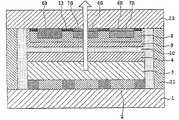
- a first preferable embodiment of the present inventionis a top emission type organic EL display as shown in FIG. 1 .
- An organic EL devicecomprising lower anodes 2 , an organic light-emitting layer 3 and an upper transparent cathode 4 is formed on a TFT substrate 1 .
- desired color-converting filter layersare formed on a transparent substrate 12 .
- blue, green and red color-converting filter layersare formed; the blue color-converting filter layers are constituted from blue color filter layers 6 B, and the green and red color-converting filter layers are constituted from laminates of color filter layers 6 G or 6 R and color-converting layers 7 G or 7 R.
- a black mask 13is formed between the color-converting filter layers.
- a protective layer 8is formed on the color-converting filter layers and the black mask, and then a passivation layer 9 is formed so as to cover the above-mentioned layers, whereby a color-converting filter substrate is obtained.
- the organic EL device and the color-converting filterare aligned and bonded together while forming a filler layer 10 therebetween, and then finally peripheral parts are sealed using a sealing resin 11 , whereby the organic EL display is obtained.
- one out of the protective layer 8 , the passivation layer 9 and the filler layer 10may have a color filter function of transmitting the color of the light emitted from the organic EL device.
- two or more of these layersmay have such a color filter function.
- two or more of the layershave a color filter function
- adjustmentis preferably carried out such that these layers as a whole have a transmissivity at wavelengths of 450 to 510 nm of 80 to 90%, and a transmissivity around 600 nm of 20 to 30%.
- the amount added of a colorant or pigment to each of these layerscan be reduced, and hence adverse effects on other properties of these layers can be suppressed.
- different colorants or pigmentsmay be added to each of the two or more layers so that a desired spectrum can be obtained overall.
- a second preferable embodiment of the present inventionis a bottom emission type organic EL display as shown in FIG. 2 .
- Desired color-converting filter layersare formed on a transparent substrate 12 .
- blue ( 6 B), green ( 6 G, 7 G) and red ( 6 R, 7 R) color-converting filter layersare formed, and the constitution thereof is the same as in the first embodiment.
- a black mask 13is formed between the color-converting filter layers.
- a protective layer 8is formed on the color-converting filter layers and the black mask, and then a passivation layer 9 is formed so as to cover the above-mentioned layers.
- An organic EL devicecomprising transparent electrodes 21 , an organic light-emitting layer 3 and upper electrodes 22 is then formed thereon.
- FIG. 2shows a constitution for carrying out passive matrix driving, with the transparent electrodes 21 and the upper electrodes 22 being formed in mutually orthogonal line patterns. Finally, the whole is sealed using a filler layer 10 , a sealing resin 11 and a sealing substrate 23 , whereby the organic EL display is obtained.
- either of the protective layer 8 and the passivation layer 9may have a color filter function of transmitting the color of the light emitted from the organic EL device.
- both of these layersmay have such a color filter function.
- adjustmentis preferably carried out such that these layers as a whole have a transmissivity at wavelengths of 450 to 510 nm of 80 to 90%, and a transmissivity around 600 nm of 20 to 30%.
- the amount added of a colorant or pigment to each of these layerscan be reduced, and hence adverse effects on other properties of these layers can be suppressed.
- different colorants or pigmentsmay be added to each of the two layers so that a desired spectrum can be obtained overall.
- the organic EL display of the present inventionmay use active matrix driving or passive matrix driving.
- active matrix drivinga constitution may be adopted in which the lower electrodes are partitioned with there being one lower electrode for each light-emitting part, and the lower electrodes are connected, for example, to the sources of TFTs provided on a substrate.
- the upper cathodecan be made to be a single unified electrode.
- passive matrix drivinga constitution can be adopted in which the lower anodes and the upper cathodes comprise patterns of lines extending in mutually orthogonal directions.
- a constructionhas been described in which a color filter function is given to a layer having another function in the organic EL display, but a layer having only such a filter function may be separately formed.
- a layer having only a filter functioncan be provided in at least positions corresponding to the color-converting filter layers of the various colors, or may be provided over the whole of the substrate.
- a base resin of the layer having only the filter functionmay be a light-curable or joint-light/heat-curable resin as with the matrix resin of the color-converting filter layers, or may be any of various resins that can be used in a protective layer.
- the layer having only the filter functioncan be formed by adding a cyan type colorant as described earlier to this base resin, and adjusting such that the layer has a transmissivity at wavelengths of 450 to 510 nm of 80 to 90%, and a transmissivity around 600 nm of 20 to 30%.
- FIG. 1a construction was adopted in which bottom gate type TFTs were formed on a glass substrate 1 , and a lower anode 2 was connected to the source of each TFT.
- Alwhich was connected to the source of the corresponding TFT via a contact hole (not shown) formed in an insulating film (not shown) on the TFT, was formed as a lower part, and IZO (InZnO) was formed on the upper surface thereof.
- the Al filmis provided to reflect light emitted from the light-emitting layer so that light is emitted efficiently from the top, and to reduce the electrical resistance.
- the thickness of the Al filmwas made to be 300 nm.
- the upper part IZOhas a high work function, and hence is provided so that holes can be injected efficiently.
- the thickness of the IZOwas made to be 200 nm.
- the substrate 1 having the lower anodes 2 formed thereonwas put into a resistive heating vapor deposition apparatus, and a hole injection layer, a hole transport layer, an organic light-emitting layer, and an electron injection layer were deposited in this order without releasing the vacuum, thus forming an organic EL device.
- CuPcCopper phthalocyanine
- ⁇ -NPD4,4′-bis[N-(1-naphthyl)-N-phenylamino]biphenyl
- DPVBi4,4′-bis(2,2-diphenylvinyl)biphenyl
- AlqAluminum tris(8-quinolinolate)
- an upper transparent cathode 4was formed using a metal mask without releasing the vacuum.
- the upper transparent cathode 4was formed by depositing metallic Mg/Ag, which has a low work function as required for injection of electrons, to a thickness of 2 nm using a codeposition method, and then depositing an IZO film thereon to a thickness of 200 nm using a sputtering method.
- a blue filter materialmade by Fuji Hunt Electronics Technology; Color Mosaic CB-7001 was applied using a spin coating method onto a transparent (glass) substrate 12 , and then patterning was carried out using a photolithography method, thus obtaining a line pattern with a thickness of 10 ⁇ m.
- Green and red color filter layers 6 G and 6 R made of similar color filter materialswere applied using a spin coating method onto the transparent substrate 12 , and then patterning was carried out using a photolithography method, thus obtaining line patterns with a thickness of 1.5 ⁇ m.
- a black mask 13(thickness 1.5 ⁇ m) was formed between the color-converting filter layers of the various colors.
- a black mask having high thermal conductivityfirst a chromium oxide layer of thickness 500 nm was formed by sputtering using a mask enabling formation of a lattice pattern on walls of the color-converting filter layers.
- an SiN filmwas formed by sputtering around the R, G and B sub-pixels so as to be the same thickness.
- the pitch of the pixelswas 0.3 ⁇ 0.3 mm, and the shape of the sub-pixels of the various colors was 0.1 ⁇ 0.3 mm.
- a matrix material of a protective layer to be formed on an upper surface of the color-converting filter layerswas made to be ZPN 1100 (made by Nippon Zeon Co., Ltd.).
- Heliogen (registered trade mark) Blue D-7565(C.I. Pigment Blue 16) was mixed and dispersed to a content of approximately 3.0 mass % into this matrix material, the dispersion was applied on using a spin coating method, and then patterning was carried out using a photolithography method, thus forming the protective layer on the color-converting filter layers.
- the thickness from the surface of the color-converting layerswas 3 ⁇ m.
- the above dispersionwas separately applied onto a glass substrate to a thickness of 3 ⁇ m, and the transmission spectrum was measured.
- the transmissivity at a wavelength of 470 nmwas 80%, and the transmissivity at a wavelength of 610 nm was 20%.
- An SiON x filmwas deposited by sputtering to a thickness of 300 nm as a passivation layer 9 .
- the TFT substrate having the organic EL layer 3 and the upper transparent cathode 4 formed on the lower anodes 2 , and the color-converting filter substrate having the color filter layers 6 , the color-converting layers 7 , the protective layer 8 and the passivation layer 9 formed thereon obtained as described abovewere bonded together using a UV-curing sealing resin 11 .
- the space between the two substrateswas filled with a material such as a silicone gel as a filler layer 10 .
- An organic EL displaywas manufactured as in Example 1, except that the Heliogen (registered trademark) Blue D-7565 pigment was not added to the protective layer, and a passivation layer was deposited to a thickness of 300 nm by sputtering using Al 2 O 3 doped with 1.0 at % of Co as a target.
- the Heliogenregistered trademark
- Blue D-7565 pigmentwas not added to the protective layer, and a passivation layer was deposited to a thickness of 300 nm by sputtering using Al 2 O 3 doped with 1.0 at % of Co as a target.
- a layer of thickness 300 nmwas separately formed on a glass substrate by sputtering using the above target, and the transmission spectrum was measured.
- the transmissivity at a wavelength of 470 nmwas 80%, and the transmissivity at a wavelength of 600 nm was 30%.
- An organic EL displaywas manufactured as in Example 1, except that the Heliogen (registered trade mark) Blue D-7565 pigment was not added to the protective layer, and a silicone gel having 3.0 mass % of the Heliogen (registered trade mark) Blue D-7565 dispersed therein was used as the filler.
- the filler layerhad a thickness of 5.0 ⁇ m at parts corresponding to the color-converting filter layers.
- the above fillerwas separately applied onto a glass substrate to a thickness of 5.0 ⁇ m, and the transmission spectrum was measured.
- the transmissivity at a wavelength of 470 nmwas 80%, and the transmissivity at a wavelength of 600 nm was 20%.
- An organic EL displaywas manufactured as in Example 1, except that the Heliogen (registered trademark) Blue D-7565 pigment was not added to the protective layer.
- the contrast ratiowas measured in accordance with the measurement method of JIS Z8513. The measurement results are shown in Table 1.
- the contrast ratiois represented as the ratio ‘brightness when emitting light: brightness when not emitting light’ for the case of 1000 l ⁇ of external light from 45°.
- the present inventioncan be used with an organic EL display.
- an organic EL displayhaving an organic EL device comprising lower electrodes, upper electrodes and an organic EL light-emitting layer therebetween, and color-converting layers that absorb light emitted from the organic EL device and carry out fluorescent conversion, or color filter layers, or color-converting filter layers comprising such color-converting layers and color filter layers formed on top of one another
- a constitutionhas been adopted in which a layer having a color filter function of transmitting only the color of the light emitted from the organic EL device is provided between the color-converting layers or color-converting filter layers and the organic EL device; as a result, out of light infiltrating into the organic EL display from the outside, the color complementary to the color of the light emitted by the organic EL device, i.e. a red/green color in the present examples, is absorbed along the way and hence does not reach the lower electrodes, whereby the amount of reflected light is reduced accordingly, and
Landscapes
- Physics & Mathematics (AREA)
- Optics & Photonics (AREA)
- Electroluminescent Light Sources (AREA)
Abstract
Description
- (1) Anodes/organic EL light-emitting layer/cathodes
- (2) Anodes/hole injection layer/organic EL light-emitting layer/cathodes
- (3) Anodes/organic EL light-emitting layer/electron injection layer/cathodes
- (4) Anodes/hole injection layer/organic EL light-emitting layer/electron injection layer/cathodes
- (5) Anodes/hole injection layer/hole transport layer/organic EL light-emitting layer/electron injection layer/cathodes
| TABLE 1 |
| Evaluation of Results |
| Contrast Ratio | ||
| Example 1 | 100:1 | ||
| Example 2 | 90:1 | ||
| Example 3 | 110:1 | ||
| Comparative | 60:1 | ||
| Example 1 | |||
Claims (15)
Applications Claiming Priority (3)
| Application Number | Priority Date | Filing Date | Title |
|---|---|---|---|
| JP2002149688 | 2002-05-23 | ||
| JP2002-149688 | 2002-05-23 | ||
| PCT/JP2003/006326WO2003101155A1 (en) | 2002-05-23 | 2003-05-21 | Organic el display |
Publications (2)
| Publication Number | Publication Date |
|---|---|
| US20050248929A1 US20050248929A1 (en) | 2005-11-10 |
| US7456570B2true US7456570B2 (en) | 2008-11-25 |
Family
ID=29561216
Family Applications (1)
| Application Number | Title | Priority Date | Filing Date |
|---|---|---|---|
| US10/515,563Expired - LifetimeUS7456570B2 (en) | 2002-05-23 | 2003-05-21 | Organic EL display having color converting filters |
Country Status (9)
| Country | Link |
|---|---|
| US (1) | US7456570B2 (en) |
| JP (1) | JPWO2003101155A1 (en) |
| KR (1) | KR100915616B1 (en) |
| CN (1) | CN1656852A (en) |
| AU (1) | AU2003242355A1 (en) |
| DE (2) | DE10392604T5 (en) |
| GB (1) | GB2404276B (en) |
| TW (1) | TWI272871B (en) |
| WO (1) | WO2003101155A1 (en) |
Cited By (6)
| Publication number | Priority date | Publication date | Assignee | Title |
|---|---|---|---|---|
| US20110024780A1 (en)* | 2009-07-28 | 2011-02-03 | Soon-Ryong Park | Organic light emitting diode display |
| US20120038267A1 (en)* | 2010-08-11 | 2012-02-16 | Seiko Epson Corporation | Organic el device, method of producing organic el device, and electronic apparatus |
| US20120086323A1 (en)* | 2010-10-11 | 2012-04-12 | Polymer Vision B.V. | Display and method and apparatus for manufacturing a display |
| US8253327B2 (en) | 2007-06-28 | 2012-08-28 | Semiconductor Energy Laboratory Co., Ltd. | Light-emitting element, light-emitting device, and electronic device |
| US8564196B2 (en) | 2009-04-09 | 2013-10-22 | Panasonic Corporation | Organic electroluminescent display device containing filter to provide high contrast |
| US11545642B2 (en) | 2014-05-30 | 2023-01-03 | Semiconductor Energy Laboratory Co., Ltd. | Light-emitting device, display device, and electronic device with color conversion layers |
Families Citing this family (37)
| Publication number | Priority date | Publication date | Assignee | Title |
|---|---|---|---|---|
| JP3865245B2 (en)* | 2003-03-12 | 2007-01-10 | 富士電機ホールディングス株式会社 | Manufacturing method and manufacturing apparatus for organic EL display |
| US7728516B2 (en) | 2003-06-13 | 2010-06-01 | Fuji Electric Holdings Co., Ltd. | Organic EL display |
| JP2005259687A (en)* | 2004-02-13 | 2005-09-22 | Kochi Univ | Color conversion filter and organic EL display using the same |
| JP3992001B2 (en)* | 2004-03-01 | 2007-10-17 | セイコーエプソン株式会社 | Organic electroluminescence device and electronic device |
| CN1969595A (en)* | 2004-08-26 | 2007-05-23 | 出光兴产株式会社 | Organic EL display device |
| US8350466B2 (en)* | 2004-09-17 | 2013-01-08 | Semiconductor Energy Laboratory Co., Ltd. | Display device and manufacturing method thereof |
| KR100635575B1 (en)* | 2004-11-17 | 2006-10-17 | 삼성에스디아이 주식회사 | full color OLED and fabricating method of the same |
| JP4552187B2 (en)* | 2004-12-02 | 2010-09-29 | 富士電機ホールディングス株式会社 | Multicolor light emitting device and manufacturing method thereof |
| US20060138941A1 (en)* | 2004-12-27 | 2006-06-29 | Osram Opto Semiconductors Gmbh | Electrolumenscent organic light emitting device and production method thereof |
| WO2006077808A1 (en)* | 2005-01-18 | 2006-07-27 | Dai Nippon Printing Co., Ltd. | Color filter substrate for organic electroluminescent device |
| JP2007115419A (en)* | 2005-10-18 | 2007-05-10 | Fuji Electric Holdings Co Ltd | Organic light emitting device |
| US8409727B2 (en)* | 2005-12-28 | 2013-04-02 | Samsung Display Co., Ltd. | Color filter array and organic light-emitting display device using the same |
| US20080042146A1 (en)* | 2006-08-18 | 2008-02-21 | Cok Ronald S | Light-emitting device having improved ambient contrast |
| JP2010517207A (en)* | 2007-01-24 | 2010-05-20 | 富士電機ホールディングス株式会社 | Color conversion layer patterning method and organic EL display manufacturing method using the same |
| JP2009032477A (en)* | 2007-07-26 | 2009-02-12 | Nippon Seiki Co Ltd | Organic el panel and its manufacturing method |
| DE102008017071A1 (en) | 2008-01-31 | 2009-08-06 | Osram Opto Semiconductors Gmbh | Optoelectronic module and projection device with the optoelectronic module |
| JP5440064B2 (en)* | 2008-10-21 | 2014-03-12 | 東芝ライテック株式会社 | Lighting device |
| JP5327601B2 (en) | 2008-12-12 | 2013-10-30 | 東芝ライテック株式会社 | Light emitting module and lighting device |
| US8408724B2 (en)* | 2008-12-26 | 2013-04-02 | Toshiba Lighting & Technology Corporation | Light source module and lighting apparatus |
| JP2010232163A (en)* | 2009-03-03 | 2010-10-14 | Fujifilm Corp | Method of manufacturing light-emitting display device, light-emitting display device, and light-emitting display |
| EP2365525A3 (en)* | 2010-03-12 | 2013-05-29 | Toshiba Lighting & Technology Corporation | Illumination apparatus having an array of red and phosphour coated blue LEDs |
| JP5670178B2 (en) | 2010-12-28 | 2015-02-18 | ユー・ディー・シー アイルランド リミテッド | Organic electroluminescence device |
| KR101773087B1 (en)* | 2011-06-17 | 2017-08-31 | 삼성디스플레이 주식회사 | Organic light-emitting display device employing black matrix-containing neutral density film |
| KR102093628B1 (en)* | 2013-10-10 | 2020-03-26 | 엘지디스플레이 주식회사 | Organic electro luminescent device and method of fabricating the same |
| KR20150086763A (en) | 2014-01-20 | 2015-07-29 | 삼성디스플레이 주식회사 | Light emitting display device and method for fabricating the same |
| DE102015107471A1 (en)* | 2015-05-12 | 2016-11-17 | Osram Oled Gmbh | Organic light emitting device |
| KR101797018B1 (en) | 2015-11-30 | 2017-11-13 | 엘지디스플레이 주식회사 | Organic light emitting display device and head mounted display including the same |
| KR102478491B1 (en)* | 2015-12-30 | 2022-12-16 | 엘지디스플레이 주식회사 | Organic Light Emitting Diode Display Device And Method Of Fabricating The Same |
| DE102016101517A1 (en) | 2016-01-28 | 2017-08-03 | Osram Oled Gmbh | Organic light emitting diode |
| KR102666206B1 (en)* | 2016-12-22 | 2024-05-14 | 엘지디스플레이 주식회사 | Display device having a color filter |
| US10768485B2 (en)* | 2017-07-05 | 2020-09-08 | Nanoco Technologies Ltd. | Quantum dot architectures for color filter applications |
| CN109728031B (en)* | 2017-10-31 | 2020-03-24 | 昆山国显光电有限公司 | Organic electroluminescent device, display and mobile communication equipment |
| CN108878497B (en)* | 2018-06-29 | 2020-05-19 | 京东方科技集团股份有限公司 | Display substrate, manufacturing method and display device |
| CN113224109A (en)* | 2020-02-06 | 2021-08-06 | 群创光电股份有限公司 | Display device |
| KR20220004889A (en)* | 2020-07-03 | 2022-01-12 | 삼성디스플레이 주식회사 | Display device |
| KR20220149858A (en)* | 2021-04-30 | 2022-11-09 | 삼성디스플레이 주식회사 | Display device |
| CN113328047B (en)* | 2021-06-02 | 2022-06-10 | 武汉天马微电子有限公司 | Display panel, manufacturing method thereof and display device |
Citations (17)
| Publication number | Priority date | Publication date | Assignee | Title |
|---|---|---|---|---|
| JPH03152897A (en) | 1989-11-09 | 1991-06-28 | Idemitsu Kosan Co Ltd | electroluminescent element |
| JPH08286033A (en) | 1995-02-13 | 1996-11-01 | Idemitsu Kosan Co Ltd | Red fluorescence conversion film and red light emitting device using the same |
| JPH09115668A (en) | 1995-10-19 | 1997-05-02 | Idemitsu Kosan Co Ltd | Emission color conversion film |
| JPH09208944A (en) | 1996-02-06 | 1997-08-12 | Idemitsu Kosan Co Ltd | Fluorescence conversion film |
| JPH10162958A (en) | 1996-11-28 | 1998-06-19 | Casio Comput Co Ltd | EL element |
| JP2000003786A (en) | 1998-06-12 | 2000-01-07 | Idemitsu Kosan Co Ltd | Organic EL display |
| US6117529A (en)* | 1996-12-18 | 2000-09-12 | Gunther Leising | Organic electroluminescence devices and displays |
| US20010050532A1 (en)* | 2000-01-31 | 2001-12-13 | Mitsuru Eida | Organic electroluminescence display device and method of manufacturing same |
| JP2002015861A (en) | 2000-04-25 | 2002-01-18 | Semiconductor Energy Lab Co Ltd | Light emitting device |
| JP2002093579A (en) | 2000-09-11 | 2002-03-29 | Sony Corp | EL element |
| US20020102480A1 (en)* | 2001-01-18 | 2002-08-01 | Fuji Photo Film Co., Ltd. | Color filter, color filter forming material and process for producing color filter |
| US20020105265A1 (en)* | 2000-03-20 | 2002-08-08 | Feng-Ju Chuang | Organic electroluminescent device and method of making same |
| US20020113241A1 (en)* | 2000-07-24 | 2002-08-22 | Tdk Corporation | Light emitting device |
| US20020122144A1 (en)* | 2000-12-25 | 2002-09-05 | Seiko Epson Corporation | Illumination device and manufacturing method therefor, display device, and electronic instrument |
| JP2003115378A (en) | 2001-07-05 | 2003-04-18 | Koninkl Philips Electronics Nv | Organic electroluminescent display device with optical filter |
| US6563263B1 (en)* | 1998-09-07 | 2003-05-13 | Fuji Electric Co., Ltd. | Multi-colored organic EL device with protective layer |
| US6573579B1 (en)* | 2002-01-22 | 2003-06-03 | Industrial Technology Research Institute | Projector employing OEL image panels |
Family Cites Families (16)
| Publication number | Priority date | Publication date | Assignee | Title |
|---|---|---|---|---|
| JPH0748424A (en) | 1989-10-06 | 1995-02-21 | Nippon Steel Corp | Epoxy acrylate resin |
| JP2813495B2 (en) | 1991-07-26 | 1998-10-22 | 出光興産株式会社 | Organic EL element sealing method |
| JPH05119306A (en) | 1991-10-25 | 1993-05-18 | A G Technol Kk | Production of color filter substrate |
| JPH05134112A (en) | 1991-11-15 | 1993-05-28 | A G Technol Kk | Formation of color filter board |
| JP3336674B2 (en) | 1993-04-13 | 2002-10-21 | 出光興産株式会社 | Method of reproducing color filter substrate and method of manufacturing color filter using the same |
| JP3405570B2 (en) | 1993-09-30 | 2003-05-12 | 出光興産株式会社 | Manufacturing method of color filter |
| JP3367081B2 (en) | 1993-11-02 | 2003-01-14 | 出光興産株式会社 | Manufacturing method of color filter |
| JPH07218717A (en) | 1994-01-28 | 1995-08-18 | Toray Ind Inc | Manufacture of color filter |
| JPH07306311A (en) | 1994-05-12 | 1995-11-21 | Asahi Glass Co Ltd | Substrate with color filter and liquid crystal display device using the same |
| JP2714763B2 (en) | 1994-07-11 | 1998-02-16 | 近藤鋼材株式会社 | Construction method of reinforced concrete structure |
| JP3187695B2 (en) | 1995-02-06 | 2001-07-11 | 出光興産株式会社 | Multicolor light emitting device and method of manufacturing the same |
| JP4011649B2 (en) | 1996-06-11 | 2007-11-21 | 出光興産株式会社 | Multicolor light emitting device and manufacturing method thereof |
| EP0845812B1 (en) | 1996-11-28 | 2009-10-28 | Casio Computer Co., Ltd. | Display apparatus |
| JP3369066B2 (en) | 1996-12-04 | 2003-01-20 | 松下電器産業株式会社 | Mobile communication base station system |
| JP3582373B2 (en) | 1998-09-09 | 2004-10-27 | 富士電機ホールディングス株式会社 | Multicolor light emitting organic EL device and method of manufacturing the same |
| EP1042775A2 (en) | 1998-09-22 | 2000-10-11 | Fed Corporation | Inorganic-based color conversion matrix element for organic color display devices and method of fabrication |
- 2003
- 2003-05-21CNCNA038116847Apatent/CN1656852A/enactivePending
- 2003-05-21GBGB0425133Apatent/GB2404276B/ennot_activeExpired - Lifetime
- 2003-05-21DEDE10392604Tpatent/DE10392604T5/enactiveGranted
- 2003-05-21USUS10/515,563patent/US7456570B2/ennot_activeExpired - Lifetime
- 2003-05-21WOPCT/JP2003/006326patent/WO2003101155A1/enactiveApplication Filing
- 2003-05-21JPJP2004507292Apatent/JPWO2003101155A1/ennot_activeWithdrawn
- 2003-05-21AUAU2003242355Apatent/AU2003242355A1/ennot_activeAbandoned
- 2003-05-21DEDE10392604.6Apatent/DE10392604B4/ennot_activeExpired - Lifetime
- 2003-05-21KRKR1020047018543Apatent/KR100915616B1/ennot_activeExpired - Lifetime
- 2003-06-11TWTW092115861Apatent/TWI272871B/ennot_activeIP Right Cessation
Patent Citations (17)
| Publication number | Priority date | Publication date | Assignee | Title |
|---|---|---|---|---|
| JPH03152897A (en) | 1989-11-09 | 1991-06-28 | Idemitsu Kosan Co Ltd | electroluminescent element |
| JPH08286033A (en) | 1995-02-13 | 1996-11-01 | Idemitsu Kosan Co Ltd | Red fluorescence conversion film and red light emitting device using the same |
| JPH09115668A (en) | 1995-10-19 | 1997-05-02 | Idemitsu Kosan Co Ltd | Emission color conversion film |
| JPH09208944A (en) | 1996-02-06 | 1997-08-12 | Idemitsu Kosan Co Ltd | Fluorescence conversion film |
| JPH10162958A (en) | 1996-11-28 | 1998-06-19 | Casio Comput Co Ltd | EL element |
| US6117529A (en)* | 1996-12-18 | 2000-09-12 | Gunther Leising | Organic electroluminescence devices and displays |
| JP2000003786A (en) | 1998-06-12 | 2000-01-07 | Idemitsu Kosan Co Ltd | Organic EL display |
| US6563263B1 (en)* | 1998-09-07 | 2003-05-13 | Fuji Electric Co., Ltd. | Multi-colored organic EL device with protective layer |
| US20010050532A1 (en)* | 2000-01-31 | 2001-12-13 | Mitsuru Eida | Organic electroluminescence display device and method of manufacturing same |
| US20020105265A1 (en)* | 2000-03-20 | 2002-08-08 | Feng-Ju Chuang | Organic electroluminescent device and method of making same |
| JP2002015861A (en) | 2000-04-25 | 2002-01-18 | Semiconductor Energy Lab Co Ltd | Light emitting device |
| US20020113241A1 (en)* | 2000-07-24 | 2002-08-22 | Tdk Corporation | Light emitting device |
| JP2002093579A (en) | 2000-09-11 | 2002-03-29 | Sony Corp | EL element |
| US20020122144A1 (en)* | 2000-12-25 | 2002-09-05 | Seiko Epson Corporation | Illumination device and manufacturing method therefor, display device, and electronic instrument |
| US20020102480A1 (en)* | 2001-01-18 | 2002-08-01 | Fuji Photo Film Co., Ltd. | Color filter, color filter forming material and process for producing color filter |
| JP2003115378A (en) | 2001-07-05 | 2003-04-18 | Koninkl Philips Electronics Nv | Organic electroluminescent display device with optical filter |
| US6573579B1 (en)* | 2002-01-22 | 2003-06-03 | Industrial Technology Research Institute | Projector employing OEL image panels |
Non-Patent Citations (1)
| Title |
|---|
| Office Action issued to a relatd Japanese Application No. 2004-507292, dated Feb. 14, 2008, and translation of relevant portions thereof. |
Cited By (10)
| Publication number | Priority date | Publication date | Assignee | Title |
|---|---|---|---|---|
| US8253327B2 (en) | 2007-06-28 | 2012-08-28 | Semiconductor Energy Laboratory Co., Ltd. | Light-emitting element, light-emitting device, and electronic device |
| US8941301B2 (en) | 2007-06-28 | 2015-01-27 | Semiconductor Energy Laboratory Co., Ltd. | Light-emitting element, light-emitting device, electronic device, and method for fabricating light-emitting element |
| US8564196B2 (en) | 2009-04-09 | 2013-10-22 | Panasonic Corporation | Organic electroluminescent display device containing filter to provide high contrast |
| US20110024780A1 (en)* | 2009-07-28 | 2011-02-03 | Soon-Ryong Park | Organic light emitting diode display |
| US9112179B2 (en) | 2009-07-28 | 2015-08-18 | Samsung Display Co., Ltd. | Organic light emitting diode display |
| US20120038267A1 (en)* | 2010-08-11 | 2012-02-16 | Seiko Epson Corporation | Organic el device, method of producing organic el device, and electronic apparatus |
| US8933623B2 (en)* | 2010-08-11 | 2015-01-13 | Seiko Epson Corporation | Organic EL device, method of producing organic EL device, and electronic apparatus |
| US20120086323A1 (en)* | 2010-10-11 | 2012-04-12 | Polymer Vision B.V. | Display and method and apparatus for manufacturing a display |
| US11545642B2 (en) | 2014-05-30 | 2023-01-03 | Semiconductor Energy Laboratory Co., Ltd. | Light-emitting device, display device, and electronic device with color conversion layers |
| US12127418B2 (en) | 2014-05-30 | 2024-10-22 | Semiconductor Energy Laboratory Co., Ltd. | Light-emitting device with color conversion layers |
Also Published As
| Publication number | Publication date |
|---|---|
| TWI272871B (en) | 2007-02-01 |
| KR100915616B1 (en) | 2009-09-07 |
| CN1656852A (en) | 2005-08-17 |
| JPWO2003101155A1 (en) | 2005-10-20 |
| KR20040111629A (en) | 2004-12-31 |
| GB2404276B (en) | 2005-08-10 |
| GB0425133D0 (en) | 2004-12-15 |
| TW200428901A (en) | 2004-12-16 |
| WO2003101155A1 (en) | 2003-12-04 |
| US20050248929A1 (en) | 2005-11-10 |
| DE10392604T5 (en) | 2005-05-12 |
| AU2003242355A1 (en) | 2003-12-12 |
| DE10392604B4 (en) | 2023-03-09 |
| GB2404276A (en) | 2005-01-26 |
Similar Documents
| Publication | Publication Date | Title |
|---|---|---|
| US7456570B2 (en) | Organic EL display having color converting filters | |
| US7119409B2 (en) | Organic el display | |
| US7339315B2 (en) | Full color organic light-emitting device having color modulation layer | |
| US20060202613A1 (en) | Organic el display | |
| US20140014941A1 (en) | Color conversion film and multicolor-emitting, organic electroluminescent device comprising the color conversion film | |
| US20070109571A1 (en) | Color filter with color conversion function, producing method thereof, and organic el display | |
| JPWO2004036960A1 (en) | Organic electroluminescence display device and manufacturing method thereof | |
| JP2003115377A (en) | Light emitting device, method of manufacturing the same, and display device using the same | |
| JP2007207656A (en) | Organic EL display | |
| JP3591728B2 (en) | Organic EL display | |
| JP3501148B2 (en) | Organic EL display | |
| JP2007115419A (en) | Organic light emitting device | |
| US6563263B1 (en) | Multi-colored organic EL device with protective layer | |
| US7294439B2 (en) | Color-converting filter and manufacturing method | |
| US20070290612A1 (en) | Light Emitting Device and Method for Producing Same | |
| JP2004103519A (en) | Color conversion color filter substrate and organic color display using the same | |
| JP3775325B2 (en) | Organic EL display | |
| JP2003264081A (en) | Red fluorescence conversion filter and organic light emitting device using the same | |
| JP2004227811A (en) | Organic EL display and manufacturing method thereof | |
| JP2009205929A (en) | Full-color organic el display panel | |
| JP5194353B2 (en) | Color filter substrate for organic electroluminescence device | |
| JP2006107836A (en) | Color conversion filter, manufacturing method thereof, and organic EL display using the same | |
| JP2002093578A (en) | Color conversion filter substrate, and color conversion type organic light emitting device and color display having color conversion filter substrate | |
| JP4552187B2 (en) | Multicolor light emitting device and manufacturing method thereof | |
| JP2006269227A (en) | Multicolor light emitting device and manufacturing method thereof |
Legal Events
| Date | Code | Title | Description |
|---|---|---|---|
| AS | Assignment | Owner name:FUJI ELECTRIC HOLDINGS CO., LTD., JAPAN Free format text:ASSIGNMENT OF ASSIGNORS INTEREST;ASSIGNORS:KAWAMURA, YUKINORI;KAWAGUCHI, KOJI;SAKURAI, KENYA;REEL/FRAME:016804/0808 Effective date:20041201 | |
| STCF | Information on status: patent grant | Free format text:PATENTED CASE | |
| FEPP | Fee payment procedure | Free format text:PAYOR NUMBER ASSIGNED (ORIGINAL EVENT CODE: ASPN); ENTITY STATUS OF PATENT OWNER: LARGE ENTITY | |
| AS | Assignment | Owner name:FUJI ELECTRIC CO., LTD., JAPAN Free format text:MERGER AND CHANGE OF NAME;ASSIGNOR:FUJI ELECTRIC HOLDINGS CO., LTD.;REEL/FRAME:026891/0655 Effective date:20110401 | |
| FPAY | Fee payment | Year of fee payment:4 | |
| AS | Assignment | Owner name:SHARP KABUSHIKI KAISHA, JAPAN Free format text:ASSIGNMENT OF ASSIGNORS INTEREST;ASSIGNOR:FUJI ELECTRIC CO., LTD.;REEL/FRAME:028486/0959 Effective date:20120608 | |
| AS | Assignment | Owner name:UNIFIED INNOVATIVE TECHNOLOGY, LLC, DELAWARE Free format text:ASSIGNMENT OF ASSIGNORS INTEREST;ASSIGNOR:SHARP KABUSHIKI KAISHA;REEL/FRAME:032874/0655 Effective date:20140421 | |
| FEPP | Fee payment procedure | Free format text:PAYOR NUMBER ASSIGNED (ORIGINAL EVENT CODE: ASPN); ENTITY STATUS OF PATENT OWNER: LARGE ENTITY Free format text:PAYER NUMBER DE-ASSIGNED (ORIGINAL EVENT CODE: RMPN); ENTITY STATUS OF PATENT OWNER: LARGE ENTITY | |
| FPAY | Fee payment | Year of fee payment:8 | |
| MAFP | Maintenance fee payment | Free format text:PAYMENT OF MAINTENANCE FEE, 12TH YEAR, LARGE ENTITY (ORIGINAL EVENT CODE: M1553); ENTITY STATUS OF PATENT OWNER: LARGE ENTITY Year of fee payment:12 | |
| AS | Assignment | Owner name:GLOBAL OLED TECHNOLOGY LLC, VIRGINIA Free format text:ASSIGNMENT OF ASSIGNORS INTEREST;ASSIGNOR:UNIFIED INNOVATIVE TECHNOLOGY, LLC;REEL/FRAME:055082/0455 Effective date:20201124 |