US7453629B2 - Semiconductor optical amplifier pulse reshaper - Google Patents
Semiconductor optical amplifier pulse reshaperDownload PDFInfo
- Publication number
- US7453629B2 US7453629B2US11/321,151US32115105AUS7453629B2US 7453629 B2US7453629 B2US 7453629B2US 32115105 AUS32115105 AUS 32115105AUS 7453629 B2US7453629 B2US 7453629B2
- Authority
- US
- United States
- Prior art keywords
- wavelength
- vcsoa
- offset
- reflective portions
- input signal
- Prior art date
- Legal status (The legal status is an assumption and is not a legal conclusion. Google has not performed a legal analysis and makes no representation as to the accuracy of the status listed.)
- Active
Links
Images


Classifications
- H—ELECTRICITY
- H01—ELECTRIC ELEMENTS
- H01S—DEVICES USING THE PROCESS OF LIGHT AMPLIFICATION BY STIMULATED EMISSION OF RADIATION [LASER] TO AMPLIFY OR GENERATE LIGHT; DEVICES USING STIMULATED EMISSION OF ELECTROMAGNETIC RADIATION IN WAVE RANGES OTHER THAN OPTICAL
- H01S5/00—Semiconductor lasers
- H01S5/04—Processes or apparatus for excitation, e.g. pumping, e.g. by electron beams
- H01S5/041—Optical pumping
- H—ELECTRICITY
- H01—ELECTRIC ELEMENTS
- H01S—DEVICES USING THE PROCESS OF LIGHT AMPLIFICATION BY STIMULATED EMISSION OF RADIATION [LASER] TO AMPLIFY OR GENERATE LIGHT; DEVICES USING STIMULATED EMISSION OF ELECTROMAGNETIC RADIATION IN WAVE RANGES OTHER THAN OPTICAL
- H01S5/00—Semiconductor lasers
- H01S5/10—Construction or shape of the optical resonator, e.g. extended or external cavity, coupled cavities, bent-guide, varying width, thickness or composition of the active region
- H01S5/12—Construction or shape of the optical resonator, e.g. extended or external cavity, coupled cavities, bent-guide, varying width, thickness or composition of the active region the resonator having a periodic structure, e.g. in distributed feedback [DFB] lasers
- H—ELECTRICITY
- H01—ELECTRIC ELEMENTS
- H01S—DEVICES USING THE PROCESS OF LIGHT AMPLIFICATION BY STIMULATED EMISSION OF RADIATION [LASER] TO AMPLIFY OR GENERATE LIGHT; DEVICES USING STIMULATED EMISSION OF ELECTROMAGNETIC RADIATION IN WAVE RANGES OTHER THAN OPTICAL
- H01S5/00—Semiconductor lasers
- H01S5/50—Amplifier structures not provided for in groups H01S5/02 - H01S5/30
- H—ELECTRICITY
- H04—ELECTRIC COMMUNICATION TECHNIQUE
- H04B—TRANSMISSION
- H04B10/00—Transmission systems employing electromagnetic waves other than radio-waves, e.g. infrared, visible or ultraviolet light, or employing corpuscular radiation, e.g. quantum communication
- H04B10/29—Repeaters
- H04B10/291—Repeaters in which processing or amplification is carried out without conversion of the main signal from optical form
- H04B10/2912—Repeaters in which processing or amplification is carried out without conversion of the main signal from optical form characterised by the medium used for amplification or processing
- H04B10/2914—Repeaters in which processing or amplification is carried out without conversion of the main signal from optical form characterised by the medium used for amplification or processing using lumped semiconductor optical amplifiers [SOA]
- H—ELECTRICITY
- H04—ELECTRIC COMMUNICATION TECHNIQUE
- H04B—TRANSMISSION
- H04B10/00—Transmission systems employing electromagnetic waves other than radio-waves, e.g. infrared, visible or ultraviolet light, or employing corpuscular radiation, e.g. quantum communication
- H04B10/29—Repeaters
- H04B10/291—Repeaters in which processing or amplification is carried out without conversion of the main signal from optical form
- H04B10/299—Signal waveform processing, e.g. reshaping or retiming
- H—ELECTRICITY
- H01—ELECTRIC ELEMENTS
- H01S—DEVICES USING THE PROCESS OF LIGHT AMPLIFICATION BY STIMULATED EMISSION OF RADIATION [LASER] TO AMPLIFY OR GENERATE LIGHT; DEVICES USING STIMULATED EMISSION OF ELECTROMAGNETIC RADIATION IN WAVE RANGES OTHER THAN OPTICAL
- H01S5/00—Semiconductor lasers
- H01S5/10—Construction or shape of the optical resonator, e.g. extended or external cavity, coupled cavities, bent-guide, varying width, thickness or composition of the active region
- H01S5/1092—Multi-wavelength lasing
- H—ELECTRICITY
- H01—ELECTRIC ELEMENTS
- H01S—DEVICES USING THE PROCESS OF LIGHT AMPLIFICATION BY STIMULATED EMISSION OF RADIATION [LASER] TO AMPLIFY OR GENERATE LIGHT; DEVICES USING STIMULATED EMISSION OF ELECTROMAGNETIC RADIATION IN WAVE RANGES OTHER THAN OPTICAL
- H01S5/00—Semiconductor lasers
- H01S5/10—Construction or shape of the optical resonator, e.g. extended or external cavity, coupled cavities, bent-guide, varying width, thickness or composition of the active region
- H01S5/18—Surface-emitting [SE] lasers, e.g. having both horizontal and vertical cavities
- H01S5/183—Surface-emitting [SE] lasers, e.g. having both horizontal and vertical cavities having only vertical cavities, e.g. vertical cavity surface-emitting lasers [VCSEL]
- H—ELECTRICITY
- H01—ELECTRIC ELEMENTS
- H01S—DEVICES USING THE PROCESS OF LIGHT AMPLIFICATION BY STIMULATED EMISSION OF RADIATION [LASER] TO AMPLIFY OR GENERATE LIGHT; DEVICES USING STIMULATED EMISSION OF ELECTROMAGNETIC RADIATION IN WAVE RANGES OTHER THAN OPTICAL
- H01S5/00—Semiconductor lasers
- H01S5/50—Amplifier structures not provided for in groups H01S5/02 - H01S5/30
- H01S5/5063—Amplifier structures not provided for in groups H01S5/02 - H01S5/30 operating above threshold
Definitions
- the inventionis related to the field of optical communications, and in particular, to semiconductor optical amplifier pulse reshapers.
- Regenerations of optical signalsare essential aspects of optical communications. Regenerations may be accomplished by re-amplification, re-shaping and re-timing through the use of optic-electronic-optic (OEO) repeaters.
- OEOoptic-electronic-optic
- OEO regenerationsare expensive and technologically complex.
- OEO regenerationsare the main approach commercially available for this task.
- a semiconductor optical amplifier (SOA) deviceincludes dual mode reflectors optically cooperating at an input signal wavelength ( ⁇ s ) and an offset wavelength ( ⁇ c ) proximate the input signal wavelength ( ⁇ s ) to provide thereby non-linear amplification of the input signal ( ⁇ s ).
- An embodiment of the inventionprovides for a semiconductor optical amplifier (SOA) pulse reshaper, including a pump for adjusting the lasing threshold and amplification of the SOA at either signal wavelength ( ⁇ s ) or offset wavelength ( ⁇ c ) which is dependent on input digital signal intensities of logical 1 and 0.
- SOAsemiconductor optical amplifier
- the SOAincludes dual mode reflectors optically cooperating at an input signal wavelength ( ⁇ s ) and an offset wavelength ( ⁇ c ) proximate the input signal wavelength ( ⁇ s ).
- a controllerfor providing thereby non-linear amplification of input signal ( ⁇ s ).
- the inventionfurther provides other methods and system elements that implement various aspects, embodiments, and features of the invention, as described in further detail below.
- FIG. 1depicts a block diagram of a dual mode vertical cavity semiconductor optical amplifier (VCSOA) according to an embodiment of the invention
- FIG. 2depicts a block diagram of a dual mode in-plane semiconductor optical amplifier according to an embodiment of the invention
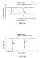
- FIG. 3Adepicts a line graph depicting the relationship of small signal gains and cavity losses to two modes (or two wavelengths) without input signal according to an embodiment of the invention
- FIG. 3Bdepicts a line graph depicting a relationship of the gains and cavity losses to the two modes (or two wavelengths) with a logic “1” input signal with appropriate optical intensity according to an embodiment of the invention
- FIG. 4depicts a line graph of signal gain as a function of input signal intensity (signal logic “0” and logic “1”) according to an embodiment of the invention.
- FIG. 5depicts a block diagram of a semiconductor optical amplifier pulse reshaper according to an embodiment of the invention.
- the inventionwill be primarily described within the context of vertical cavity semiconductor optical amplifier pulse reshaper; however, those skilled in the art and informed by the teachings herein will realize that the invention is also applicable to any apparatus and method that involves regeneration of optical signals in, for example, a communication network.
- This inventionmay be utilized to replace the OEO regeneration approach with a SOA reshaper that can remarkably reduce both the cost and the complexity of the system.
- Embodiments of the inventioncan be easily integrated in front of optical receivers and/or behind other types of optical amplifiers, while providing small power consumption and footprint to improve system performance as well as simplicity.
- FIG. 1depicts a block diagram of a dual mode vertical cavity semiconductor optical amplifier (VCSOA) 100 according to an embodiment of the invention.
- the VCSOA 100comprises four layers: a substrate layer 110 , a first dual mode distributed Bragg reflector (DBR) mirror 120 , an active region 130 , and a second dual mode DBR mirror 140 .
- DBRdistributed Bragg reflector
- the bottom layer of the four layersthe substrate 110 .
- the next layer above the substrateis the first dual mode DBR 120 layer.
- the next layer above the first DBR layeris the active region 130 .
- the top layeris the second dual mode DBR layer 140 .
- the input lightis transmitted into the VCSOA from the top of layer 140 .
- the input lightenters the active region 130 .
- the active region 130amplifies the input light by reflecting the light between the first and second DBR mirrors 120 and 140 , and by pumping the region with the pump light 170 .
- the pump light 170transfers the pump energy into signal optical energy.
- the structure of the two DBRs at both ends of the active regionproduces wavelength-selective reflections where the light in the active region 130 is amplified.
- Lthe effective cavity length
- ⁇the wavelength of the specific mode
- the amplified output light exiting the VCSOA from the top DBR layer 140is 180 degree out of phase with respect to the part of input light that is reflected-off the surface of the top DBR layer 140 .
- the reflected-off input lightis the portion of light that is reflected off the top DBR layer 140 without entering the VCSOA.
- the final output of the SOAshould be the interfering result of the amplified output light and the reflected-off input light.
- DBR mirrors 120 and 140each include two portions 180 , 190 .
- a first portionreflects a first wavelength and a second portion reflects a second wavelength.
- the VCSOAhas 2 reflective wavelengths and two modes of operation.
- the dual mode VCSOAreceives an input optical signal ⁇ s 150 .
- the output optical signals 160have wavelengths of ⁇ S and ⁇ C .
- One wavelength ⁇ Sis the same wavelength as the input signal and the other ⁇ C is separated by a small offset.
- the two wavelength outputsare amplitude modulated by each other and are interleaved in time domain with logic zeros and ones.
- the offsetis selected to be small enough to obtain strong interaction between the two modes.
- the wavelength offsetis a value between ⁇ 0.4 nm and ⁇ 4.0 nm. In other embodiments, other amounts of offset are used.
- the offset valuesare varied by the selection of the reflective portions of the DBR mirrors as well as the effective cavity length for this offset mode.
- FIG. 2depicts a block diagram of a dual-mode in-plane semiconductor optical amplifier (SOA) according to an embodiment of the invention.
- the in-plane SOAhas four layers: a first substrate layer 210 , an active medium layer 220 , a distributed feedback (DFB) layer 230 , and a second substrate layer 240 .
- a first substrate layer 210the in-plane SOA has four layers: a first substrate layer 210 , an active medium layer 220 , a distributed feedback (DFB) layer 230 , and a second substrate layer 240 .
- DFBdistributed feedback
- the in-plane SOAreceives as input an optical signal 250 and provides at an output an amplified optical signal 260 .
- the bottom and top layers 210 , 240are substrate layers, which functions as the ground and contact, respectively.
- the DFB layer 230includes a wavelength selective Bragg grating.
- the active medium 220is in close proximity with the DFB layer.
- the input optical signalresonantly diffracts back and forth in the in-plane SOA.
- An amplified optical signal 260exits the in-plane SOA.
- the in-plane SOAhas two modes that allow two wavelengths to resonate. Similar to the DBR mirrors in FIG. 1 , the DFB layer of in-plan SOA has two reflective wavelengths or two modes of operation. The grating of the DFB will determine the two modes of the in-plane SOA.
- the dual mode in-plane SOAreceives an input optical signal ⁇ s 250 .
- the output optical signals 160will have wavelengths of ⁇ S and ⁇ c .
- One wavelength ⁇ Sis the same wavelength as the input signal and the other ⁇ C is separated by a small offset.
- the two wavelength outputsare amplitude modulated by each other (i.e. mutual modulation) and are interleaved in time domain with logic zeros and ones.
- the preferred wavelength offsetis between ⁇ 0.4 nm and ⁇ 4.0 nm. In other embodiments, other amounts of offset are possible.
- the offset valuesare varied by the selection of the reflective portions of the DFB layer.
- the two types of SOA'scan both be used as pulse reshaper.
- the VCSOAis use in an embodiment.
- the VCSOAwill be used to further describe the invention.
- FIG. 3Adepicts a line graph depicting the relationship of small signal gains and cavity losses of two modes (or two wavelengths) without input signal according to an embodiment of the invention.
- the X-axisrepresents the wavelength; the Y-axis represents cavity loss and cavity small signal gain of the VCSOA. In one embodiment, the wavelength is measured in nanometer (nm); the loss and gain are measured in dB.
- the solid linerepresents the relative cavity loss over wavelength; the dotted line represents relative cavity small signal gain over wavelength.
- the structure as designedwill have the cavity small signal gain and cavity loss characteristics as shown by the dotted line and solid line respectively. At ⁇ S there is smaller loss, represented by a dip in the curve.
- the wavelength ⁇ Cwhen there is no input signal, the wavelength ⁇ C has a greater gain than loss so it lases and clamps the VCSOA at deep saturation condition because the VCSOA is designed to have as small as possible cavity loss for this clamp mode (the clamp mode is equivalent to the offset mode in this document).
- the loss at wavelength ⁇ Sis greater than the gain at that so the SOA does not laze at ⁇ S .
- the graph of FIG. 3Adepicts the condition equivalent to the optical input signal having a logical “0” as the input when there is only optical noise is injected. Full extinction of the signal output can be obtained by designing the two DBR mirrors so that the reflected-off input signal interferes with the amplified output signal thereby no light is produced from the VCSOA as output for logic “0”.
- the cavity parametersshould satisfy:
- FIG. 3Bdepicts a line graph depicting a relationship of the gains and cavity losses of the two modes (or two wavelengths) with a logic “1” input signal with appropriate optical intensity according to an embodiment of the invention.
- the X-axisrepresents the wavelengths of the input signal and the Y-axis represents the cavity losses and the cavity saturated gains at the respective wavelengths.
- the wavelengthis measured in nanometer (nm) and the gain is measured in dB.
- the solid linerepresents the cavity losses at the respective wavelengths on the X-axis, and the dotted line represents the cavity saturation gains at the respective wavelengths.
- FIG. 4depicts a line graph of signal gain as a function of input signal intensity (signal logic “0” and logic “1”) according to an embodiment of the invention.
- the graph of FIG. 4illustrates that the competition between the two modes results in non-linear gain profile over input signal intensity with regard to signal logic “0” and logic “1”.
- the gainis graphed on the Y-axis, and input intensity is on the X-axis.
- the output gainwill initially be flat and very low, which represents the logic “0.” As the input signal intensity approaches the threshold, the gain jumps up into a high level, representing logic “1.” After crossing the threshold, the gain flattens again representing a constant high gain, signifying logic “1.”
- the thresholdis adjusted by the reflectivities of the DBRs for the two modes and the pump level. The pump intensity is optimized according to the input intensity of the signal and the geometry of the cavity and structures. Thus, the transition between the logic “0” and logic “1” will occur at the desired point, and the optical signal pulse is reshaped.
- the reflectivities of either the aforementioned DBR or DFB layer for the offset wavelengthis higher than the input signal wavelength which results in a higher cavity loss for the signal wavelength (signal mode) than the offset wavelength (clamp mode) to implement non-linear amplification of input signal ( ⁇ S ) by means of competition between the two modes.
- the DBR or DFRobtains higher in-cavity optical resonating intensity for the clamp mode.
- the DBR or DFBclamps the gain medium layer of the SOA working in deep saturation condition and has higher response speed (higher data rate of the optical signal to be reamplified and reshaped).
- the“smallest” loss design for the clamp mode and the high intensity input for optical signal “1”result in faster response.
- the designallows higher data rate input optical signal to be reamplified and reshaped by the VCSOA.
- the SOA deviceis activated by choosing a pumping level above clamp mode lasing threshold and under signal mode lasing threshold.
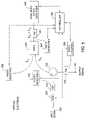
- FIG. 5depicts a block diagram of a semiconductor optical amplifier pulse reshaper 500 according to an embodiment of the invention.
- the embodiment of FIG. 5depicts a module having four photodetectors 560 , 520 , 580 , 547 , three taps 510 , 570 , 545 , a circulator 530 , a wavelength division multiplexer (WDM) 540 , a variable optical attenuator (VOA) 505 , a dual mode VCSOA with pump 550 and a controller 590 .
- WDMwavelength division multiplexer
- VOAvariable optical attenuator
- An optical input signal 150enters the pulse reshaper and travels to tap 510 where photo detector 520 obtains the power level of the optical input signal and transmits the characteristic data to the controller 590 .
- the circulator 530circulates the input signal and passes the input signal through the WDM 540 and tap 545 into the dual mode VCSOA with pump 550 .
- the VCSOA 550functions as described above.
- the output of the VCSOAcontains two wavelengths ⁇ S and ⁇ C , which enters the tap 545 with portion of the powers of the two wavelengths directed to the photo detector 547 .
- the photo detector 547transmits the characteristics of the sum of the powers of the two wavelengths to the controller 590 .
- the output of the VCSOAthen continues to the WDM 540 where the two wavelengths are separated onto two different paths.
- the WDM 540directs optical signal ⁇ C to photo detector 560 .
- the power level characteristics of the optical signal ⁇ Care transmitted to controller 590 .
- the WDM 540also directs the optical signal ⁇ S back to the circulator 530 where the optical signal is circulated to tap 570 .
- the tap 570directs a part of the signal to photodetector 580 where the output signal power level characteristics is obtained and is sent to controller 590 .
- the controllerhaving the characteristics of the input signal, output signal, ⁇ C signal, and the sum of the powers of the two wavelengths from output of the VCSOA, analyzes the information and respectively adjust the pump of the VCSOA 550 and the VOA 505 in order to obtain the desired output gain profile.
- the fourth photodetector 547obtains the sum of the powers of both the clamp mode output and the signal mode output as P 0 , and a signal is present at input port of the SOA pulse reshaper, then the input signal power is adjusted by the VOA.
- the adjustment to the VOAsuppresses the clamp mode power level (which is obtained by photo detector 560 ).
- the adjustment to the VOAis P 0 /2 for non-return to zero data format and to d*P 0 /2 for return to zero data format, with insertion losses of the WDM and tap in the optical paths calibrated-out from the detected power levels, wherein “d” is the duty cycle of the return to zero data format.
- the pulse reshaperis used in telecommunication equipment because it reamplifies and reshapes the optical pulses for both NRZ (non-return to zero) and RZ (return to zero) data format.
Landscapes
- Physics & Mathematics (AREA)
- Electromagnetism (AREA)
- Condensed Matter Physics & Semiconductors (AREA)
- General Physics & Mathematics (AREA)
- Optics & Photonics (AREA)
- Engineering & Computer Science (AREA)
- Computer Networks & Wireless Communication (AREA)
- Signal Processing (AREA)
- Optical Communication System (AREA)
Abstract
Description
- where:
- gsis single pass gain;
- Rtis top DBR reflectivity for λs;
- Rbis bottom DBR reflectivity for λs.
this full extinction condition means that the optical noise contained within the logic “0” time slot is eliminated at VCSOA output.
Claims (16)
Priority Applications (2)
| Application Number | Priority Date | Filing Date | Title |
|---|---|---|---|
| US11/321,151US7453629B2 (en) | 2005-12-29 | 2005-12-29 | Semiconductor optical amplifier pulse reshaper |
| US12/187,542US7692853B2 (en) | 2005-12-29 | 2008-08-07 | Semiconductor optical amplifier pulse reshaper |
Applications Claiming Priority (1)
| Application Number | Priority Date | Filing Date | Title |
|---|---|---|---|
| US11/321,151US7453629B2 (en) | 2005-12-29 | 2005-12-29 | Semiconductor optical amplifier pulse reshaper |
Related Child Applications (1)
| Application Number | Title | Priority Date | Filing Date |
|---|---|---|---|
| US12/187,542DivisionUS7692853B2 (en) | 2005-12-29 | 2008-08-07 | Semiconductor optical amplifier pulse reshaper |
Publications (2)
| Publication Number | Publication Date |
|---|---|
| US20070153365A1 US20070153365A1 (en) | 2007-07-05 |
| US7453629B2true US7453629B2 (en) | 2008-11-18 |
Family
ID=38224068
Family Applications (2)
| Application Number | Title | Priority Date | Filing Date |
|---|---|---|---|
| US11/321,151ActiveUS7453629B2 (en) | 2005-12-29 | 2005-12-29 | Semiconductor optical amplifier pulse reshaper |
| US12/187,542Expired - Fee RelatedUS7692853B2 (en) | 2005-12-29 | 2008-08-07 | Semiconductor optical amplifier pulse reshaper |
Family Applications After (1)
| Application Number | Title | Priority Date | Filing Date |
|---|---|---|---|
| US12/187,542Expired - Fee RelatedUS7692853B2 (en) | 2005-12-29 | 2008-08-07 | Semiconductor optical amplifier pulse reshaper |
Country Status (1)
| Country | Link |
|---|---|
| US (2) | US7453629B2 (en) |
Cited By (2)
| Publication number | Priority date | Publication date | Assignee | Title |
|---|---|---|---|---|
| US20100092175A1 (en)* | 2008-10-10 | 2010-04-15 | Electronics And Telecommunications Research Institute | Reflective semiconductor optical amplifier and optical signal processing method using the same |
| US20210194205A1 (en)* | 2016-02-29 | 2021-06-24 | Tokyo Institute Of Technology | Surface-emitting laser |
Families Citing this family (2)
| Publication number | Priority date | Publication date | Assignee | Title |
|---|---|---|---|---|
| US9608758B1 (en)* | 2015-11-30 | 2017-03-28 | Google Inc. | Low cost gain clamped EDFA for TWDM passive optical network application |
| KR102801220B1 (en)* | 2020-03-17 | 2025-04-30 | 삼성전자주식회사 | Light source module and display panel using the same |
Citations (8)
| Publication number | Priority date | Publication date | Assignee | Title |
|---|---|---|---|---|
| US3467906A (en)* | 1967-06-14 | 1969-09-16 | Rca Corp | Constant-gain low-noise light amplifier |
| US5754578A (en)* | 1996-06-24 | 1998-05-19 | W. L. Gore & Associates, Inc. | 1250-1650 nm vertical cavity surface emitting laser pumped by a 700-1050 nm vertical cavity surface emitting laser |
| US6252896B1 (en)* | 1999-03-05 | 2001-06-26 | Agilent Technologies, Inc. | Long-Wavelength VCSEL using buried bragg reflectors |
| US6330265B1 (en)* | 1998-04-21 | 2001-12-11 | Kabushiki Kaisha Toshiba | Optical functional element and transmission device |
| US6407855B1 (en)* | 1999-10-29 | 2002-06-18 | Sdl, Inc. | Multiple wavelength optical sources |
| US6445495B1 (en)* | 1999-03-22 | 2002-09-03 | Genoa Corporation | Tunable-gain lasing semiconductor optical amplifier |
| US6577435B1 (en)* | 1998-11-10 | 2003-06-10 | Electronics And Telecommunications Research Institute | Optical wavelength converter based on cross-gain modulation with wide input power dynamic range |
| US6947206B2 (en) | 2003-07-18 | 2005-09-20 | Kailight Photonics, Inc. | All-optical, tunable regenerator, reshaper and wavelength converter |
Family Cites Families (1)
| Publication number | Priority date | Publication date | Assignee | Title |
|---|---|---|---|---|
| US6836357B2 (en)* | 2001-10-04 | 2004-12-28 | Gazillion Bits, Inc. | Semiconductor optical amplifier using laser cavity energy to amplify signal and method of fabrication thereof |
- 2005
- 2005-12-29USUS11/321,151patent/US7453629B2/enactiveActive
- 2008
- 2008-08-07USUS12/187,542patent/US7692853B2/ennot_activeExpired - Fee Related
Patent Citations (8)
| Publication number | Priority date | Publication date | Assignee | Title |
|---|---|---|---|---|
| US3467906A (en)* | 1967-06-14 | 1969-09-16 | Rca Corp | Constant-gain low-noise light amplifier |
| US5754578A (en)* | 1996-06-24 | 1998-05-19 | W. L. Gore & Associates, Inc. | 1250-1650 nm vertical cavity surface emitting laser pumped by a 700-1050 nm vertical cavity surface emitting laser |
| US6330265B1 (en)* | 1998-04-21 | 2001-12-11 | Kabushiki Kaisha Toshiba | Optical functional element and transmission device |
| US6577435B1 (en)* | 1998-11-10 | 2003-06-10 | Electronics And Telecommunications Research Institute | Optical wavelength converter based on cross-gain modulation with wide input power dynamic range |
| US6252896B1 (en)* | 1999-03-05 | 2001-06-26 | Agilent Technologies, Inc. | Long-Wavelength VCSEL using buried bragg reflectors |
| US6445495B1 (en)* | 1999-03-22 | 2002-09-03 | Genoa Corporation | Tunable-gain lasing semiconductor optical amplifier |
| US6407855B1 (en)* | 1999-10-29 | 2002-06-18 | Sdl, Inc. | Multiple wavelength optical sources |
| US6947206B2 (en) | 2003-07-18 | 2005-09-20 | Kailight Photonics, Inc. | All-optical, tunable regenerator, reshaper and wavelength converter |
Non-Patent Citations (3)
| Title |
|---|
| E. Staffan, et al., "Long Wavelength Vertical-Cavity Semiconductor Optical Amplifiers," IEEE J. of Quantum Electronics, vol. 37, No. 2, Feb. 2001, pp. 274-281. |
| M. T. Hill et al., "Carrier Recovery Time in Semiconductor Optical Amplifiers That Employ Holding Beams," Optics Letters, vol. 27, No. 18, Sep. 15, 2002, pp. 1625-1627. |
| Y. Liu et al., "Wavelength Conversion Using Nonlinear Polarization Rotation in a Single Semiconductor Optical Amplifier," IEEE Photonics Tech. Lett., vol. 15, No. 1, Jan. 2003, pp. 90-92. |
Cited By (3)
| Publication number | Priority date | Publication date | Assignee | Title |
|---|---|---|---|---|
| US20100092175A1 (en)* | 2008-10-10 | 2010-04-15 | Electronics And Telecommunications Research Institute | Reflective semiconductor optical amplifier and optical signal processing method using the same |
| US8149503B2 (en)* | 2008-10-10 | 2012-04-03 | Electronics And Telecommunications Research Institute | Reflective semiconductor optical amplifier and optical signal processing method using the same |
| US20210194205A1 (en)* | 2016-02-29 | 2021-06-24 | Tokyo Institute Of Technology | Surface-emitting laser |
Also Published As
| Publication number | Publication date |
|---|---|
| US20070153365A1 (en) | 2007-07-05 |
| US7692853B2 (en) | 2010-04-06 |
| US20080310013A1 (en) | 2008-12-18 |
Similar Documents
| Publication | Publication Date | Title |
|---|---|---|
| US6577654B1 (en) | Optical signal power monitor and regulator | |
| US6597497B2 (en) | Semiconductor optical amplifier with transverse laser cavity intersecting optical signal path and method of fabrication thereof | |
| US6445495B1 (en) | Tunable-gain lasing semiconductor optical amplifier | |
| CN110459956B (en) | Narrow linewidth tunable laser | |
| US6891664B2 (en) | Multistage tunable gain optical amplifier | |
| EP4042529B1 (en) | Wavelength control of multi-wavelength laser | |
| US7692853B2 (en) | Semiconductor optical amplifier pulse reshaper | |
| KR20040040708A (en) | Optical Wavelength Converting Apparatus based on XGM for High Extinction Ratio and Wide Input Power Dynamic Range | |
| US20030063646A1 (en) | Semiconductor laser device, semiconductor laser module, and semiconductor laser control method | |
| US7065300B1 (en) | Optical transmitter including a linear semiconductor optical amplifier | |
| JP3989374B2 (en) | Light control device | |
| US6792215B1 (en) | Multiwavelength light source device employing annular optical delay circuit | |
| US7110169B1 (en) | Integrated optical device including a vertical lasing semiconductor optical amplifier | |
| KR20040106676A (en) | Gain clamped semiconductor optical amplifier using raman gain mechanism | |
| US7009760B2 (en) | Optical 2R/3R regeneration | |
| Suzuki et al. | Application of a lambda/4-shifted DFB laser/electroabsorption modulator monolithically integrated light source to single-chip pulse generator with variable repetition rate | |
| Kimura et al. | High-temperature characteristics and tunability of long-wavelength vertical-cavity semiconductor optical amplifiers | |
| KR100617686B1 (en) | Gain Fixed Semiconductor Optical Amplifiers | |
| EP1176459B1 (en) | Optical threshold and comparison devices and methods | |
| JP4653940B2 (en) | Light controller for communication | |
| JP4242864B2 (en) | Wavelength converter for generating a tunable laser light source by itself | |
| Verma et al. | Developments in linear optical amplifier technology | |
| JP3287443B2 (en) | Semiconductor laser capable of polarization modulation and optical communication system using the same | |
| Akın et al. | Selective filtering and amplification of THz-range optical signals with an on-chip multi-wavelength DBR laser | |
| Björlin et al. | 1.3 µm vertical-cavity amplifying switch |
Legal Events
| Date | Code | Title | Description |
|---|---|---|---|
| AS | Assignment | Owner name:LUCENT TECHNOLOGIES INC., NEW JERSEY Free format text:ASSIGNMENT OF ASSIGNORS INTEREST;ASSIGNORS:DAI, HONGXING;WANG, PENG;YING, JINPIN;REEL/FRAME:017429/0805;SIGNING DATES FROM 20051221 TO 20051227 | |
| STCF | Information on status: patent grant | Free format text:PATENTED CASE | |
| FPAY | Fee payment | Year of fee payment:4 | |
| AS | Assignment | Owner name:CREDIT SUISSE AG, NEW YORK Free format text:SECURITY INTEREST;ASSIGNOR:ALCATEL-LUCENT USA INC.;REEL/FRAME:030510/0627 Effective date:20130130 | |
| AS | Assignment | Owner name:ALCATEL-LUCENT USA INC., NEW JERSEY Free format text:RELEASE BY SECURED PARTY;ASSIGNOR:CREDIT SUISSE AG;REEL/FRAME:033950/0001 Effective date:20140819 | |
| FPAY | Fee payment | Year of fee payment:8 | |
| AS | Assignment | Owner name:OMEGA CREDIT OPPORTUNITIES MASTER FUND, LP, NEW YORK Free format text:SECURITY INTEREST;ASSIGNOR:WSOU INVESTMENTS, LLC;REEL/FRAME:043966/0574 Effective date:20170822 Owner name:OMEGA CREDIT OPPORTUNITIES MASTER FUND, LP, NEW YO Free format text:SECURITY INTEREST;ASSIGNOR:WSOU INVESTMENTS, LLC;REEL/FRAME:043966/0574 Effective date:20170822 | |
| AS | Assignment | Owner name:WSOU INVESTMENTS, LLC, CALIFORNIA Free format text:ASSIGNMENT OF ASSIGNORS INTEREST;ASSIGNOR:ALCATEL LUCENT;REEL/FRAME:044000/0053 Effective date:20170722 | |
| AS | Assignment | Owner name:BP FUNDING TRUST, SERIES SPL-VI, NEW YORK Free format text:SECURITY INTEREST;ASSIGNOR:WSOU INVESTMENTS, LLC;REEL/FRAME:049235/0068 Effective date:20190516 | |
| AS | Assignment | Owner name:WSOU INVESTMENTS, LLC, CALIFORNIA Free format text:RELEASE BY SECURED PARTY;ASSIGNOR:OCO OPPORTUNITIES MASTER FUND, L.P. (F/K/A OMEGA CREDIT OPPORTUNITIES MASTER FUND LP;REEL/FRAME:049246/0405 Effective date:20190516 | |
| MAFP | Maintenance fee payment | Free format text:PAYMENT OF MAINTENANCE FEE, 12TH YEAR, LARGE ENTITY (ORIGINAL EVENT CODE: M1553); ENTITY STATUS OF PATENT OWNER: LARGE ENTITY Year of fee payment:12 | |
| AS | Assignment | Owner name:OT WSOU TERRIER HOLDINGS, LLC, CALIFORNIA Free format text:SECURITY INTEREST;ASSIGNOR:WSOU INVESTMENTS, LLC;REEL/FRAME:056990/0081 Effective date:20210528 | |
| AS | Assignment | Owner name:WSOU INVESTMENTS, LLC, CALIFORNIA Free format text:RELEASE BY SECURED PARTY;ASSIGNOR:TERRIER SSC, LLC;REEL/FRAME:056526/0093 Effective date:20210528 |