US7453160B2 - Simplified wafer alignment - Google Patents
Simplified wafer alignmentDownload PDFInfo
- Publication number
- US7453160B2 US7453160B2US10/830,734US83073404AUS7453160B2US 7453160 B2US7453160 B2US 7453160B2US 83073404 AUS83073404 AUS 83073404AUS 7453160 B2US7453160 B2US 7453160B2
- Authority
- US
- United States
- Prior art keywords
- wafer
- radiation
- arm
- amount
- alignment
- Prior art date
- Legal status (The legal status is an assumption and is not a legal conclusion. Google has not performed a legal analysis and makes no representation as to the accuracy of the status listed.)
- Active, expires
Links
- 239000004065semiconductorSubstances0.000claimsabstractdescription23
- 230000007246mechanismEffects0.000claimsdescription17
- 230000005855radiationEffects0.000claimsdescription17
- 238000011109contaminationMethods0.000claimsdescription10
- 238000012545processingMethods0.000claimsdescription10
- 239000002245particleSubstances0.000claimsdescription9
- 230000008859changeEffects0.000claimsdescription4
- 238000012546transferMethods0.000claimsdescription4
- XLYOFNOQVPJJNP-UHFFFAOYSA-NwaterSubstancesOXLYOFNOQVPJJNP-UHFFFAOYSA-N0.000claims1
- 235000012431wafersNutrition0.000abstractdescription180
- 238000004519manufacturing processMethods0.000abstractdescription11
- 238000009987spinningMethods0.000abstractdescription8
- 239000000356contaminantSubstances0.000abstractdescription5
- 150000002500ionsChemical class0.000description26
- 238000000034methodMethods0.000description12
- 239000000758substrateSubstances0.000description12
- 230000005465channelingEffects0.000description7
- 230000008569processEffects0.000description7
- 239000002019doping agentSubstances0.000description6
- 238000002513implantationMethods0.000description5
- 238000010884ion-beam techniqueMethods0.000description5
- 239000000463materialSubstances0.000description5
- XUIMIQQOPSSXEZ-UHFFFAOYSA-NSiliconChemical compound[Si]XUIMIQQOPSSXEZ-UHFFFAOYSA-N0.000description3
- 239000013078crystalSubstances0.000description3
- 229910052710siliconInorganic materials0.000description3
- 239000010703siliconSubstances0.000description3
- 230000002411adverseEffects0.000description2
- 230000004075alterationEffects0.000description2
- 230000008901benefitEffects0.000description2
- 238000005468ion implantationMethods0.000description2
- 238000012986modificationMethods0.000description2
- 230000004048modificationEffects0.000description2
- 238000005280amorphizationMethods0.000description1
- 238000013459approachMethods0.000description1
- 230000000712assemblyEffects0.000description1
- 238000000429assemblyMethods0.000description1
- 239000002178crystalline materialSubstances0.000description1
- 238000010586diagramMethods0.000description1
- 229910003460diamondInorganic materials0.000description1
- 239000010432diamondSubstances0.000description1
- 230000000694effectsEffects0.000description1
- 239000007943implantSubstances0.000description1
- 230000006872improvementEffects0.000description1
- 239000012535impuritySubstances0.000description1
- 230000002452interceptive effectEffects0.000description1
- 230000000116mitigating effectEffects0.000description1
- 239000000203mixtureSubstances0.000description1
- NJPPVKZQTLUDBO-UHFFFAOYSA-NnovaluronChemical compoundC1=C(Cl)C(OC(F)(F)C(OC(F)(F)F)F)=CC=C1NC(=O)NC(=O)C1=C(F)C=CC=C1FNJPPVKZQTLUDBO-UHFFFAOYSA-N0.000description1
- 238000012856packingMethods0.000description1
Images


Classifications
- H—ELECTRICITY
- H01—ELECTRIC ELEMENTS
- H01L—SEMICONDUCTOR DEVICES NOT COVERED BY CLASS H10
- H01L21/00—Processes or apparatus adapted for the manufacture or treatment of semiconductor or solid state devices or of parts thereof
- H01L21/67—Apparatus specially adapted for handling semiconductor or electric solid state devices during manufacture or treatment thereof; Apparatus specially adapted for handling wafers during manufacture or treatment of semiconductor or electric solid state devices or components ; Apparatus not specifically provided for elsewhere
- H01L21/67005—Apparatus not specifically provided for elsewhere
- H01L21/67242—Apparatus for monitoring, sorting or marking
- H01L21/67259—Position monitoring, e.g. misposition detection or presence detection
- H—ELECTRICITY
- H01—ELECTRIC ELEMENTS
- H01L—SEMICONDUCTOR DEVICES NOT COVERED BY CLASS H10
- H01L2223/00—Details relating to semiconductor or other solid state devices covered by the group H01L23/00
- H01L2223/544—Marks applied to semiconductor devices or parts
- H01L2223/54426—Marks applied to semiconductor devices or parts for alignment
- Y—GENERAL TAGGING OF NEW TECHNOLOGICAL DEVELOPMENTS; GENERAL TAGGING OF CROSS-SECTIONAL TECHNOLOGIES SPANNING OVER SEVERAL SECTIONS OF THE IPC; TECHNICAL SUBJECTS COVERED BY FORMER USPC CROSS-REFERENCE ART COLLECTIONS [XRACs] AND DIGESTS
- Y10—TECHNICAL SUBJECTS COVERED BY FORMER USPC
- Y10S—TECHNICAL SUBJECTS COVERED BY FORMER USPC CROSS-REFERENCE ART COLLECTIONS [XRACs] AND DIGESTS
- Y10S414/00—Material or article handling
- Y10S414/135—Associated with semiconductor wafer handling
Definitions
- the present inventionrelates generally to semiconductor fabrication, and more particularly to a technique for simplifying wafer alignment.
- Wafers used in semiconductor fabricationare typically formed from a crystalline material, such as bulk silicon.
- a crystalline materialsuch as bulk silicon.
- boulesvery specific types of single crystals of silicon, known as boules, are grown into long lengths and thin slices (e.g., wafers) are cut there-from.
- the crystalline structure of the wafersis advantageous in forming semiconductor devices because it facilitates control over the electrical properties of the devices and exhibits uniform electrical performance throughout the entire semiconductor material. Additionally, because impurities that degrade device performance tend to collect around irregularities in the atomic structure of a material, the regularity of the crystalline structure provides for very predictable device performance and yield.
- the wafersIn forming semiconductor devices on silicon wafers, the wafers generally go through many fabrication stages. Consequently, the wafers may pass through different semiconductor processing tools one or more times.
- One such toolis an ion implanter. Ion implanters are utilized to selectively bombard regions of a wafer with ions of a dopant material. The ions penetrate into the wafer and alter the composition thereof, thus giving the regions of the wafer particular electrical characteristics, such a may be useful for fashioning certain semiconductor devices, such as transistors, upon the wafer.
- the orientation of a wafer relative to a processing toolcan be important.
- ion implantersit may be desirable to “align” the wafer with a beam of dopant ions so that few ions encounter the lattice structure of the wafer and the ions are thereby implanted relatively deeply into the wafer or substrate.
- the deviations from the nominal lattice orientation and the dimensions of features formed upon the wafercan affect shadowing, and adversely impact the implantation process and resulting semiconductor devices.
- wafersgenerally possess some indicia of their lattice structure.
- the wafersare usually designated with Miller Index data, such as 1,0,0, which is indicative of a nominal lattice structure of the wafer relative to the mechanical or cut surface of the wafer.
- the wafersalso typically have a feature that denotes the axis of the wafer crystal. This feature is often a notch or a flat edge along the outer perimeter of the wafer.
- the number of features and orientation relative to each otherare used to denote the crystal type of the wafer and are controlled by Semiconductor Equipment and Materials International (SEMI) specifications. Larger wafer sizes (e.g., 200 and 300 mm) have generally standardized on a notch rather than a flat edge.
- SEMISemiconductor Equipment and Materials International
- a number of commercial alignersare available and generally operate by placing a wafer on the aligner by a robot.
- the waferis captured by some mechanism that allows the wafer to spin. This spinning is used to pass the perimeter of the wafer through some type of sensor to locate the notch.
- a traditional method of capturing the waferis to use a vacuum chuck located at the center of wafer.
- itcan be difficult to also capture the wafer via vacuum.
- backside contaminationcan become problematic as one or more wafers may have to pass through the same or different tools multiple times during the fabrication process. This may require multiple re-alignments whereby contaminants such as particles may get transferred to the aligner and the backsides of the wafers. Such contaminants can adversely affect subsequent processing and ultimately degrade device performance.
- Edge grip alignersare also being used. Edge grip aligners have the advantage of low backside contamination, but have the disadvantage of interfering with the edge of the wafer that is being scanned. In some cases, locating the notch requires re-clamping at a different location and therefore reducing throughput. Once the notch is located, the wafer is generally rotated again to a pre-determined orientation relative to the notch. Typically this orientation is a value that is communicated to the aligner and it may vary batch to batch depending on process conditions.
- Conventional alignersmay also provide a centering capability.
- a centering ringcan be actuated to mechanically center the wafer after the wafer has been placed on the aligner by the robot.
- Other alignerscan locate the center of the wafer during the alignment process and provide the true center position. Regardless, after the notch has been located and the wafer center has been found, the same or a different robot can retrieve the wafer (e.g., by picking the wafer at a new location that is the wafer center) and maneuver it to a fabrication tool.
- the present inventionis directed to aligning wafers within semiconductor fabrication tools. More particularly, one or more aspects of the present invention pertain to quickly and efficiently finding an alignment marking, such as an alignment notch, on a wafer to allow the wafer to be appropriately oriented within an alignment tool. Unlike conventional systems, the notch is located without firmly holding and spinning or rotating the wafer. Exposure to considerable backside contaminants is thereby mitigated and the complexity and/or cost associated with aligning the wafer is thereby reduced.
- an alignment markingsuch as an alignment notch
- a systemis disclosed that is adapted to locate an alignment marking on a semiconductor wafer.
- the systemincludes a shaft and a sleeve moveably mounted upon the shaft.
- One or more support pinsare mounted to one end of the shaft and are adapted to support a wafer situated thereon.
- An arm memberis operatively coupled to the sleeve, and an end of the arm member extends up toward the wafer when the wafer resides on the one or more support pins.
- the end of the arm memberis operative to establish a beam of radiation that may be intersected by the perimeter of the wafer.
- the wafercan thus be scanned by rotating the arm member around the perimeter of the wafer and the marking can be identified by a change in the amount of radiation transmitted past the wafer.
- a mechanism adapted to locate an alignment marking on a semiconductor waferincludes a support structure for holding the wafer, the support structure contacting a small amount of surface area of a backside of the wafer to mitigate particle contamination.
- the mechanismalso includes a member that moves relative to the wafer to detect the alignment marking.
- a method of detecting an alignment marking located on a perimeter of a waferincludes holding the wafer on a support structure that contacts a small amount of surface area of a backside of the wafer to mitigate particle contamination. The method also includes moving a member around the wafer to detect the alignment marking.
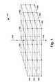
- FIG. 1is a perspective view of an example of a portion of a lattice structure wherein an ion beam is directed at the lattice structure at an angle substantially equal to ninety degrees.
- FIG. 2is a perspective view of an example of a portion of a lattice structure, such as that depicted in FIG. 1 , wherein an ion beam is directed at the lattice structure at an angle other than about ninety degrees.
- FIG. 3is a cross-sectional side view of a portion of a semiconductor substrate or wafer having features formed thereon that are separated by varying distances and that experience shadowing effects to varying degrees during ion implantation.
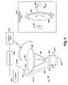
- FIG. 4illustrates an exemplary system suitable for identifying an alignment mark in accordance with one or more aspects of the present invention.
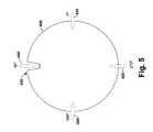
- FIG. 5illustrates an exemplary top view of a wafer and a beam of light shining on the wafer at various locations around the wafer's perimeter.
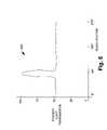
- FIG. 6is a graphical depiction of an amount of light transmitted through a wafer versus a location of a beam of light directed at the wafer, and may correspond to the exemplary arrangement illustrated in FIG. 5 .
- FIG. 7is another exemplary top view of a wafer and a beam of light shining on the wafer at various locations around the wafer's perimeter.
- FIG. 8is another graphical depiction of an amount of light transmitted past a wafer versus a location of a beam of light directed at the wafer, and may correspond to the exemplary arrangement illustrated in FIG. 7 .
- the present inventionis directed to aligning wafers within semiconductor fabrication tools. More particularly, one or more aspects of the present invention pertain to quickly and efficiently finding an alignment marking, such as an alignment notch, on a wafer to allow the wafer to be appropriately oriented within an alignment tool. Unlike conventional systems, the notch is located without firmly holding and spinning or rotating the wafer. Exposure to considerable backside contaminants is thereby mitigated and the complexity and/or cost associated with aligning the wafer is thereby reduced.
- an alignment markingsuch as an alignment notch
- a wafermay have to be aligned in a particular manner in an ion implanter to achieve a desired level of channeling and/or shadowing.
- FIG. 1a portion of a generic lattice structure 100 having a generally cubic configuration is illustrated.
- the lattice structure 100has twenty-seven (e.g., three by three by three) cells 102 that are themselves all generally cubical in shape. It is to be appreciated, however, that lattice structures can come in any of a variety of different configurations and can have any number of cells having any number of a variety of different shapes, such as diamond, pyramidal, hexagonal, etc.
- the direction of a beam of dopant ions 104 in FIG. 1is substantially perpendicular to a plane of the lattice structure such that the beam may pass there-through without encountering many, if any, portions of the lattice structure.
- the ionsmay be implanted somewhat deeply within the substrate. This may or may not be desirable depending upon the resulting electrical characteristics. It can be appreciated that other aspects can also affect channeling, such as the degree of amorphization of the substrate, the atomic mass of the substrate and the mass and/or energy of ions within the beam, for example. For instance, the greater the mass and/or energy of the ions within the beam 104 , the more likely the ions may be implanted deeply into the substrate.
- the direction of the beam 104is not substantially perpendicular to a plane of the lattice structure 100 .
- some of the ions within the ion beam 104will likely encounter portions 106 of the lattice structure and either lose energy and/or be slowed down thereby or be reflected or deflected away from these portions as indicated by arrows 108 , and thereby come to rest in shallow portions of the implanted material.
- shadowingAnother consideration regarding wafer alignment in an implantation tool is shadowing.
- a continuing trend in the electronics industryis to scale down electronic devices to produce smaller, yet more powerful devices (e.g., cell phones, digital cameras, etc.) that can perform a greater number of increasingly complex functions with less power.
- semiconductor components, such as transistors, and features thereofare continually reduced in size and formed closer together. This increased “packing” can lead to shadowing, however, whereby portions of the wafer to be doped receive little to no dopant ions. Additionally, such shadowing can become exaggerated where an implantation angle is increased, such as to diminish channeling, for example.
- a cross sectional view of a portion of a semiconductor substrate or wafer 300has a plurality of features 302 , 304 , 306 , 308 formed thereon, and respective spacings 310 , 312 , 314 defined between the features.
- the features 302 , 304 , 306 , 308are all of substantially the same height.
- Some of the resist features 302 , 304 , 306 , 308are, however, formed closer together than others, and thus the corresponding spacings 310 , 312 , 314 there-between are of different widths.
- Areas 320 , 322 , 324 of the substrate 300 exposed by the spacings 310 , 312 , 314are doped via an ion implantation tool.
- one or more ion beams 330are directed at the substrate 300 to perform the doping.
- the beams 330are directed at an angle (e.g., to mitigate channeling) and thus have a portion of their ions blocked by areas (e.g., corners) of the features 302 , 304 , 306 , 308 .
- regions 350 , 352 , 354 within the substrate areas 320 , 322 , 324receive less than intended amounts of dopant ions.
- Ion implantershave the ability to re-orient a wafer while the wafer is in a processing position.
- Ion implanterscan, for example, rotate a wafer between different implantation steps.
- a “quad” implantmay be performed whereby a wafer is repeatedly rotated and implanted with ions. This may be done, for example, to more thoroughly dope areas 320 , 322 , 324 between features 302 , 304 , 306 , 308 that would otherwise be insufficiently and/or unevenly doped.
- the addition of a motor axis within processing toolsmay also enable a change in the twist angle, either by spinning the wafer or by combining control of two axis of tilt to set the tilt and twist orientation.
- an alignment mechanismis implemented where a wafer need not be rotated to find an alignment notch.
- the waferis instead scanned by an instrument that moves around the stationary wafer. Since the wafer does not have to move, it need not be held tightly in place (e.g., via vacuum). Rather, the wafer can rest on a few pins, for example. This significantly mitigates the opportunity for particle transfer and backside contamination. Not having to rotate the wafer also reduces equipment costs among other things. Additionally, scanning a stationary wafer can greatly improve cycle times by mitigating centripetal concerns associated with spinning the wafer at high speeds. Not having to “re-grip” and/or re-orient wafers also helps to mitigate costs and improves cycle times and yields.
- the alignment mechanism 400includes a shaft 402 and a sleeve 404 moveably (e.g., rotateably) mounted around the shaft 402 .
- One or more support pins 406are also mounted upon one end of the shaft 402 .
- the support pins 406are operable to hold a wafer 408 that rests thereon.
- An arm member 410is operatively coupled to the sleeve 404 and extends up towards the wafer 408 .
- An end 414 of the arm 410 near the wafer 408has one or more protrusions 418 that extend there-from.
- One or more of the protrusions 418are adapted to establish a beam of light or other type radiation 420 there-between that may be intersected by a perimeter of the wafer 408 .
- the mechanism 400is adapted to locate an identifying notch 422 within the wafer 408 .
- the sleeve 404allows the arm 410 to rotate around the shaft 402 in a controllable manner. This allows the arm 410 , and more particularly the beam of light 420 , to “scan” the perimeter of the wafer 408 .
- the notch 422may be identified when the beam of light 420 is no longer wholly or partially interrupted by the perimeter of the wafer 408 which intersects the beam 420 .
- the end 414 of the arm 410may also, for example, be moved closer to or further away from the wafer 408 , such as via one or more pivot points 426 (e.g., that can be controlled by a motor (not shown)). This allows the end 414 of the arm 410 to extend more or less of the beam of light 420 onto the wafer 408 . It will be appreciated that the size of the alignment notch 422 is exaggerated in the Figs. for purposes of illustration and that alignment notches generally comprise a gap of only around one millimeter.
- a robotic arm 430may then pick the wafer 408 up and move it to a processing tool 432 , such as an ion implanter.
- the wafer 408may be placed upon some type of clamping mechanism 434 , such as an electrostatic clamp, to be held in place within the tool 432 .
- the tool 432may have the ability to twist the wafer 408 via a rotateable shaft 438 , as well as to tilt the wafer 408 via some type of maneuverable platform (e.g., to allow a beam of ions 440 directed at the wafer 408 to establish more evenly implanted areas within the wafer 408 and mitigate shadowing).
- U.S. Pat. No. 4,975,586 to Raydiscloses an exemplary end station and components thereof in slightly greater detail, where the end station has a wafer support or holder that is maneuverable about multiple axes. The entirety of this patent is thus hereby fully incorporated by reference.
- a controller or CPU 450may be included to control the operation of the alignment mechanism 400 .
- the controller 450may be an integral part of the mechanism 400 and/or operatively coupled thereto (e.g., via hardwiring and/or rf signals 452 ).
- the controller 450can, for example, regulate the speed at which the arm 410 rotates about the wafer 408 and/or the closeness of the end 414 of the arm 410 to the wafer 408 (e.g., by controlling a motor (not shown) operatively coupled to the sleeve 404 ).
- Such a controller 450can also take readings from sensors (not shown) within the protrusions 418 , for example, to ascertain how the beam of light 420 is being affected by the perimeter of the wafer 408 (e.g., how much light is being “blocked” and/or allowed to pass by the wafer 408 ).
- the controller 450can similarly be coupled to an optional display 454 and the robotic arm 430 to control data that is presented on the display 454 , and to direct the initial placement of the wafer 408 upon the pins 406 as well as how and when the robotic arm 430 picks up the wafer 408 and moves it to the tool 432 .
- the arm 410can start scanning the wafer at an initialization position (e.g., of zero degrees) and proceed to rotate around the wafer 408 . Once the notch 422 is found, a determination can be made as to where the notch is relative to the initialization position of the wafer 408 (e.g., 138 degrees). Thus, the robotic arm 430 can then pick the wafer 408 up knowing where the notch is located and transfer the wafer to the tool 432 and appropriately place it on a pedestal, for example. This data may also be communicated to the tool 432 so that the wafer 408 can be appropriately oriented therein (e.g., via rotateable shaft 438 ). Alternatively, since the controller 450 knows the notch location, the controller may control the manner in which the robotic arm 430 picks up the wafer 408 for placement on the clamp 434 such that little or no rotation at shaft 438 is needed.
- an initialization positione.g., of zero degrees
- FIG. 5illustrates a top view of a wafer 408 being scanned in the mechanism 400 .
- the beam 420is illustrated at several scanned locations around the perimeter of the wafer 408 , namely an initialization position of zero degrees, and at 90 degrees, 180 degrees and 270 degrees.
- the beamhas a substantially elliptical cross section. It will be appreciated, however, that the beam can have any suitable configuration. Additionally, in the example shown, not all of the beam 420 is intersected by the perimeter of the wafer 408 .
- the beammay, for example, be about a centimeter wide where about one half of the beam is blocked by the wafer and one half of the beam 420 is allowed to pass through to a beam detector.
- Other configurations and arrangements, however,may be employed and are contemplated as falling within the scope of the present invention.
- FIG. 6is an exemplary plot 600 of light transmitted past the wafer 408 versus scanned locations of the wafer 408 .
- the plotmay, for example, correspond to the situation depicted in FIG. 5 .
- the scanned location of the wafer 408is set forth on the x-axis, while the amount of light transmitted past the wafer 408 is set forth on the y-axis.
- the amount of transmitted lightcan be detected by a sensor situated, for example, on a protrusion 418 extending under or over the wafer 408 .
- a sensorwould likely be situated opposite a light emitting source situated on an opposite protrusion extending over or under the wafer 408 , respectively.
- FIG. 7illustrates a top view of a wafer 408 that is not centered in the mechanism 400 .
- different amounts of the beam 420fall upon the wafer 408 at various locations around the wafer's perimeter. For instance, very little of the beam 420 encounters the wafer 408 at the initialization position of zero degrees.
- the alignment notch 422notwithstanding, more and more of the beam gets blocked by the wafer as the scan proceeds over to the 180 degree position. After that, less and less of the beam 420 is blocked by the wafer as the scan returns to the zero degree position.
- the mechanism 400can utilize this data to ascertain the center of the wafer 408 .
- the robotic arm 430can then maneuver the wafer 408 as desired (e.g., to center the wafer 408 upon the pins 406 ). Additionally, or in the alternative, this information can be passed on to the fabrication tool 432 so that the wafer 408 can be suitably oriented (e.g., rotated) therein.
- FIG. 8is an exemplary plot 800 of transmitted light that may correspond, for example, to the situation depicted in FIG. 7 .
- the scanned location of the wafer 408is set forth on the x-axis, while the amount of light transmitted past the wafer 408 is set forth on the y-axis.
- the percent of transmitted lightbegins to gradually decrease.
- the percent of transmitted lightjumps from about 50 percent to nearly 100 percent, which is indicative of the beam 420 encountering the notch 422 .
- the amount of transmitted lightthen gradually falls back to about zero as the scan approaches the 180 degree position. More and more light is then allowed to pass by the wafer as the scan moves on to the 270 degree position and eventually back to the initialization position of zero or 360 degrees.
- one or more aspects of the present inventionallow a semiconductor fabrication tool to use acquired information and/or data to rotate or otherwise maneuver the wafer at a process position based on existing hardware rather than requiring the aligner to rotate the wafer.
- a semiconductor fabrication toolto use acquired information and/or data to rotate or otherwise maneuver the wafer at a process position based on existing hardware rather than requiring the aligner to rotate the wafer.
- the speed of rotation within the alignment mechanism 400e.g., the arm 410
- the speed of rotation within the alignment mechanism 400can be very fast and limited by motor drives and data acquisition times rather than particle concerns.
- a readoutcan also be used to determine the center of the wafer and this information can be provided to the tool such that a robot is able to retrieve the wafer correctly centered.
- This systemhas application to tool types that allow for individually setting the wafer orientation at the process position or at an intermediate position between the aligner and the process station.
- One or more aspects of the inventionthus provide a wafer alignment function with a lower cost, lower backside particle contamination and faster cycle times, among other things, as compared to conventional systems.
Landscapes
- Engineering & Computer Science (AREA)
- Physics & Mathematics (AREA)
- Condensed Matter Physics & Semiconductors (AREA)
- General Physics & Mathematics (AREA)
- Manufacturing & Machinery (AREA)
- Computer Hardware Design (AREA)
- Microelectronics & Electronic Packaging (AREA)
- Power Engineering (AREA)
- Container, Conveyance, Adherence, Positioning, Of Wafer (AREA)
Abstract
Description
Claims (15)
Priority Applications (7)
| Application Number | Priority Date | Filing Date | Title |
|---|---|---|---|
| US10/830,734US7453160B2 (en) | 2004-04-23 | 2004-04-23 | Simplified wafer alignment |
| KR1020067024618AKR20070007946A (en) | 2004-04-23 | 2005-04-25 | Simplified wafer alignment |
| EP05742593AEP1741126B1 (en) | 2004-04-23 | 2005-04-25 | Simplified wafer alignment |
| PCT/US2005/013916WO2005106925A1 (en) | 2004-04-23 | 2005-04-25 | Simplified wafer alignment |
| JP2007509691AJP5206940B2 (en) | 2004-04-23 | 2005-04-25 | Simplify wafer placement |
| CN200580012844.7ACN100468617C (en) | 2004-04-23 | 2005-04-25 | Simplified Wafer Alignment |
| DE602005023972TDE602005023972D1 (en) | 2004-04-23 | 2005-04-25 | SIMPLIFIED WAFER ALIGNMENT |
Applications Claiming Priority (1)
| Application Number | Priority Date | Filing Date | Title |
|---|---|---|---|
| US10/830,734US7453160B2 (en) | 2004-04-23 | 2004-04-23 | Simplified wafer alignment |
Publications (2)
| Publication Number | Publication Date |
|---|---|
| US20050251279A1 US20050251279A1 (en) | 2005-11-10 |
| US7453160B2true US7453160B2 (en) | 2008-11-18 |
Family
ID=34967693
Family Applications (1)
| Application Number | Title | Priority Date | Filing Date |
|---|---|---|---|
| US10/830,734Active2025-11-19US7453160B2 (en) | 2004-04-23 | 2004-04-23 | Simplified wafer alignment |
Country Status (7)
| Country | Link |
|---|---|
| US (1) | US7453160B2 (en) |
| EP (1) | EP1741126B1 (en) |
| JP (1) | JP5206940B2 (en) |
| KR (1) | KR20070007946A (en) |
| CN (1) | CN100468617C (en) |
| DE (1) | DE602005023972D1 (en) |
| WO (1) | WO2005106925A1 (en) |
Cited By (8)
| Publication number | Priority date | Publication date | Assignee | Title |
|---|---|---|---|---|
| US20080023654A1 (en)* | 2006-07-28 | 2008-01-31 | Michael Graf | Method of reducing transient wafer temperature during implantation |
| US20080157407A1 (en)* | 2005-07-06 | 2008-07-03 | Taiwan Semiconductor Manufacturing Co., Ltd. | Three dimensional ic device and alignment methods of ic device substrates |
| US20180090360A1 (en)* | 2016-09-29 | 2018-03-29 | SCREEN Holdings Co., Ltd. | Substrate alignment apparatus, substrate processing apparatus, substrate arrangement apparatus, substrate alignment method, substrate processing method, and substrate arrangement method |
| US10300554B2 (en) | 2017-01-31 | 2019-05-28 | Illumina, Inc. | Wafer alignment method and system |
| US10720354B2 (en)* | 2018-08-28 | 2020-07-21 | Axcelis Technologies, Inc. | System and method for aligning light-transmitting birefringent workpieces |
| US10794694B2 (en) | 2017-10-25 | 2020-10-06 | Axcelis Technologies, Inc. | Shallow angle, multi-wavelength, multi-receiver, adjustable sensitivity aligner sensor for semiconductor manufacturing equipment |
| US11673275B2 (en) | 2019-02-08 | 2023-06-13 | Yaskawa America, Inc. | Through-beam auto teaching |
| WO2025123052A1 (en)* | 2023-12-07 | 2025-06-12 | Axcelis Technologies, Inc. | System and method of verifying workpiece alignment |
Families Citing this family (16)
| Publication number | Priority date | Publication date | Assignee | Title |
|---|---|---|---|---|
| US7453160B2 (en)* | 2004-04-23 | 2008-11-18 | Axcelis Technologies, Inc. | Simplified wafer alignment |
| JP4522360B2 (en)* | 2005-12-02 | 2010-08-11 | 日東電工株式会社 | Semiconductor wafer position determination method and apparatus using the same |
| US7812325B2 (en)* | 2006-09-28 | 2010-10-12 | Varian Semiconductor Equipment Associates, Inc. | Implanting with improved uniformity and angle control on tilted wafers |
| US7808657B2 (en)* | 2007-06-28 | 2010-10-05 | International Business Machines Corporation | Wafer and stage alignment using photonic devices |
| TW200917401A (en)* | 2007-10-12 | 2009-04-16 | Youngtek Electronics Corp | Wafer testing system |
| JP4766156B2 (en)* | 2009-06-11 | 2011-09-07 | 日新イオン機器株式会社 | Ion implanter |
| CN102103335B (en)* | 2009-12-18 | 2012-10-10 | 和舰科技(苏州)有限公司 | Method for inspecting wafer alignment |
| JP5477133B2 (en)* | 2010-04-09 | 2014-04-23 | 日新イオン機器株式会社 | Wafer handling method and ion implantation apparatus |
| CN102315086B (en)* | 2010-06-30 | 2013-09-25 | 中芯国际集成电路制造(北京)有限公司 | Device for improving movement accuracy of mechanical arm and use method thereof |
| CN104249992B (en)* | 2013-06-28 | 2016-08-10 | 上海华虹宏力半导体制造有限公司 | Alignment methods between wafer and wafer |
| CN103531509A (en)* | 2013-09-26 | 2014-01-22 | 苏州经贸职业技术学院 | Method for precisely positioning circle center on workbench |
| CN106289199B (en)* | 2016-11-08 | 2021-06-08 | 佛山科学技术学院 | A positioning aligner |
| CN108333298B (en)* | 2017-01-19 | 2021-03-09 | 上海新昇半导体科技有限公司 | Wafer placing device and wafer orientation instrument |
| KR102217780B1 (en) | 2018-06-12 | 2021-02-19 | 피에스케이홀딩스 (주) | Alignment Apparatus |
| CN112713107B (en)* | 2020-12-16 | 2022-12-27 | 华虹半导体(无锡)有限公司 | Semiconductor wafer notch recognition device and recognition method |
| CN118483874B (en)* | 2023-02-10 | 2025-08-26 | 上海芯上微装科技股份有限公司 | Substrate transfer mechanism and exposure stage system |
Citations (19)
| Publication number | Priority date | Publication date | Assignee | Title |
|---|---|---|---|---|
| US5608223A (en) | 1994-06-10 | 1997-03-04 | Eaton Corporation | Ion implantation device |
| US6126380A (en)* | 1997-08-04 | 2000-10-03 | Creative Design Corporation | Robot having a centering and flat finding means |
| US6222196B1 (en) | 1998-11-19 | 2001-04-24 | Axcelis Technologies, Inc. | Rotatable workpiece support including cyclindrical workpiece support surfaces for an ion beam implanter |
| US20010029082A1 (en)* | 2000-03-22 | 2001-10-11 | Nikon Corporation | Charged-particle-beam microlithography apparatus including selectable systems for determining alignment-mark position, and device-fabrication methods utilizing same |
| US20020009900A1 (en)* | 1999-12-21 | 2002-01-24 | Tay Sing Pin | Growth of ultrathin nitride on Si (100) by rapid thermal N2 treatment |
| US6428399B1 (en)* | 1994-05-23 | 2002-08-06 | Sumitomo Electric Industries, Ltd. | Polishing apparatus for polishing a hard material-coated wafer |
| US20020113218A1 (en)* | 1994-02-22 | 2002-08-22 | Masahiko Okumura | Method and apparatus for positioning substrate and the like |
| US20030010280A1 (en)* | 2001-07-09 | 2003-01-16 | Shigenori Sugihara | Epitaxial semiconductor wafer and a manufacturing method thereof |
| US6537836B2 (en)* | 1999-07-28 | 2003-03-25 | Infineon Technologies Ag | Semiconductor structures and manufacturing methods |
| US6555832B1 (en) | 1999-10-13 | 2003-04-29 | Applied Materials, Inc. | Determining beam alignment in ion implantation using Rutherford Back Scattering |
| US6577382B2 (en)* | 1997-12-03 | 2003-06-10 | Nikon Corporation | Substrate transport apparatus and method |
| US20030124820A1 (en)* | 2001-04-12 | 2003-07-03 | Johnsgard Kristian E. | Systems and methods for epitaxially depositing films on a semiconductor substrate |
| US6633046B1 (en) | 2000-04-19 | 2003-10-14 | Applied Materials, Inc. | Method and apparatus for detecting that two moveable members are correctly positioned relatively to one another |
| US6727980B2 (en)* | 1998-09-17 | 2004-04-27 | Nikon Corporation | Apparatus and method for pattern exposure and method for adjusting the apparatus |
| US6778275B2 (en)* | 2002-02-20 | 2004-08-17 | Micron Technology, Inc. | Aberration mark and method for estimating overlay error and optical aberrations |
| US6888260B2 (en)* | 2003-04-17 | 2005-05-03 | Infineon Technologies Aktiengesellschaft | Alignment or overlay marks for semiconductor processing |
| US6944517B2 (en)* | 2003-07-03 | 2005-09-13 | Brooks Automation, Inc. | Substrate apparatus calibration and synchronization procedure |
| US20050251279A1 (en)* | 2004-04-23 | 2005-11-10 | Ray Andrew M | Simplified wafer alignment |
| US7348275B2 (en)* | 2005-07-11 | 2008-03-25 | Disco Corporation | Processing method for semiconductor wafer |
Family Cites Families (9)
| Publication number | Priority date | Publication date | Assignee | Title |
|---|---|---|---|---|
| JPS59147444A (en)* | 1983-02-14 | 1984-08-23 | Hitachi Ltd | Method and apparatus for positioning tabular body |
| US5982986A (en)* | 1995-02-03 | 1999-11-09 | Applied Materials, Inc. | Apparatus and method for rotationally aligning and degassing semiconductor substrate within single vacuum chamber |
| JP3741462B2 (en)* | 1995-07-18 | 2006-02-01 | 大日本スクリーン製造株式会社 | Substrate notch detection apparatus and substrate processing apparatus |
| JP3552178B2 (en)* | 1995-09-27 | 2004-08-11 | 大日本スクリーン製造株式会社 | Substrate storage cassette, interface mechanism and substrate processing device |
| JPH10242250A (en)* | 1997-02-26 | 1998-09-11 | Fujitsu Ltd | Wafer position detection method, alignment device, and semiconductor processing device |
| JP2000068357A (en)* | 1998-08-25 | 2000-03-03 | Kobe Steel Ltd | Wafer cut-out position detector and wafer characteristic measuring apparatus |
| JP3072484B2 (en)* | 1998-10-28 | 2000-07-31 | ローツェ株式会社 | Wafer positioning device |
| SG96579A1 (en)* | 2000-10-24 | 2003-06-16 | Advanced Systems Automation | Method and apparatus for a laser system for severing semiconductor wafers |
| DE10217028C1 (en)* | 2002-04-11 | 2003-11-20 | Nanophotonics Ag | Measuring module for wafer production plants |
- 2004
- 2004-04-23USUS10/830,734patent/US7453160B2/enactiveActive
- 2005
- 2005-04-25CNCN200580012844.7Apatent/CN100468617C/ennot_activeExpired - Fee Related
- 2005-04-25DEDE602005023972Tpatent/DE602005023972D1/ennot_activeExpired - Lifetime
- 2005-04-25EPEP05742593Apatent/EP1741126B1/ennot_activeExpired - Lifetime
- 2005-04-25WOPCT/US2005/013916patent/WO2005106925A1/enactiveApplication Filing
- 2005-04-25KRKR1020067024618Apatent/KR20070007946A/ennot_activeWithdrawn
- 2005-04-25JPJP2007509691Apatent/JP5206940B2/ennot_activeExpired - Fee Related
Patent Citations (20)
| Publication number | Priority date | Publication date | Assignee | Title |
|---|---|---|---|---|
| US20020113218A1 (en)* | 1994-02-22 | 2002-08-22 | Masahiko Okumura | Method and apparatus for positioning substrate and the like |
| US6428399B1 (en)* | 1994-05-23 | 2002-08-06 | Sumitomo Electric Industries, Ltd. | Polishing apparatus for polishing a hard material-coated wafer |
| US5608223A (en) | 1994-06-10 | 1997-03-04 | Eaton Corporation | Ion implantation device |
| US6126380A (en)* | 1997-08-04 | 2000-10-03 | Creative Design Corporation | Robot having a centering and flat finding means |
| US6577382B2 (en)* | 1997-12-03 | 2003-06-10 | Nikon Corporation | Substrate transport apparatus and method |
| US6727980B2 (en)* | 1998-09-17 | 2004-04-27 | Nikon Corporation | Apparatus and method for pattern exposure and method for adjusting the apparatus |
| US6222196B1 (en) | 1998-11-19 | 2001-04-24 | Axcelis Technologies, Inc. | Rotatable workpiece support including cyclindrical workpiece support surfaces for an ion beam implanter |
| US20050181575A1 (en)* | 1999-07-28 | 2005-08-18 | Christian Summerer | Semiconductor structures and manufacturing methods |
| US6537836B2 (en)* | 1999-07-28 | 2003-03-25 | Infineon Technologies Ag | Semiconductor structures and manufacturing methods |
| US6555832B1 (en) | 1999-10-13 | 2003-04-29 | Applied Materials, Inc. | Determining beam alignment in ion implantation using Rutherford Back Scattering |
| US20020009900A1 (en)* | 1999-12-21 | 2002-01-24 | Tay Sing Pin | Growth of ultrathin nitride on Si (100) by rapid thermal N2 treatment |
| US20010029082A1 (en)* | 2000-03-22 | 2001-10-11 | Nikon Corporation | Charged-particle-beam microlithography apparatus including selectable systems for determining alignment-mark position, and device-fabrication methods utilizing same |
| US6633046B1 (en) | 2000-04-19 | 2003-10-14 | Applied Materials, Inc. | Method and apparatus for detecting that two moveable members are correctly positioned relatively to one another |
| US20030124820A1 (en)* | 2001-04-12 | 2003-07-03 | Johnsgard Kristian E. | Systems and methods for epitaxially depositing films on a semiconductor substrate |
| US20030010280A1 (en)* | 2001-07-09 | 2003-01-16 | Shigenori Sugihara | Epitaxial semiconductor wafer and a manufacturing method thereof |
| US6778275B2 (en)* | 2002-02-20 | 2004-08-17 | Micron Technology, Inc. | Aberration mark and method for estimating overlay error and optical aberrations |
| US6888260B2 (en)* | 2003-04-17 | 2005-05-03 | Infineon Technologies Aktiengesellschaft | Alignment or overlay marks for semiconductor processing |
| US6944517B2 (en)* | 2003-07-03 | 2005-09-13 | Brooks Automation, Inc. | Substrate apparatus calibration and synchronization procedure |
| US20050251279A1 (en)* | 2004-04-23 | 2005-11-10 | Ray Andrew M | Simplified wafer alignment |
| US7348275B2 (en)* | 2005-07-11 | 2008-03-25 | Disco Corporation | Processing method for semiconductor wafer |
Cited By (11)
| Publication number | Priority date | Publication date | Assignee | Title |
|---|---|---|---|---|
| US20080157407A1 (en)* | 2005-07-06 | 2008-07-03 | Taiwan Semiconductor Manufacturing Co., Ltd. | Three dimensional ic device and alignment methods of ic device substrates |
| US8232659B2 (en)* | 2005-07-06 | 2012-07-31 | Taiwan Semiconductor Manufacturing Co., Ltd. | Three dimensional IC device and alignment methods of IC device substrates |
| US20080023654A1 (en)* | 2006-07-28 | 2008-01-31 | Michael Graf | Method of reducing transient wafer temperature during implantation |
| US20180090360A1 (en)* | 2016-09-29 | 2018-03-29 | SCREEN Holdings Co., Ltd. | Substrate alignment apparatus, substrate processing apparatus, substrate arrangement apparatus, substrate alignment method, substrate processing method, and substrate arrangement method |
| US10229848B2 (en)* | 2016-09-29 | 2019-03-12 | SCREEN Holdings Co., Ltd. | Substrate alignment apparatus, substrate processing apparatus, substrate arrangement apparatus, substrate alignment method, substrate processing method, and substrate arrangement method |
| US10300554B2 (en) | 2017-01-31 | 2019-05-28 | Illumina, Inc. | Wafer alignment method and system |
| US10486264B2 (en) | 2017-01-31 | 2019-11-26 | Illumina, Inc. | Wafer alignment method and system |
| US10794694B2 (en) | 2017-10-25 | 2020-10-06 | Axcelis Technologies, Inc. | Shallow angle, multi-wavelength, multi-receiver, adjustable sensitivity aligner sensor for semiconductor manufacturing equipment |
| US10720354B2 (en)* | 2018-08-28 | 2020-07-21 | Axcelis Technologies, Inc. | System and method for aligning light-transmitting birefringent workpieces |
| US11673275B2 (en) | 2019-02-08 | 2023-06-13 | Yaskawa America, Inc. | Through-beam auto teaching |
| WO2025123052A1 (en)* | 2023-12-07 | 2025-06-12 | Axcelis Technologies, Inc. | System and method of verifying workpiece alignment |
Also Published As
| Publication number | Publication date |
|---|---|
| WO2005106925A1 (en) | 2005-11-10 |
| EP1741126A1 (en) | 2007-01-10 |
| US20050251279A1 (en) | 2005-11-10 |
| JP5206940B2 (en) | 2013-06-12 |
| DE602005023972D1 (en) | 2010-11-18 |
| CN1947223A (en) | 2007-04-11 |
| JP2007535148A (en) | 2007-11-29 |
| CN100468617C (en) | 2009-03-11 |
| EP1741126B1 (en) | 2010-10-06 |
| KR20070007946A (en) | 2007-01-16 |
Similar Documents
| Publication | Publication Date | Title |
|---|---|---|
| US7453160B2 (en) | Simplified wafer alignment | |
| EP1955357B1 (en) | Ion implantation beam angle calibration | |
| TW201834140A (en) | Wafer edge lift pin design for semiconductor component manufacturing | |
| JP5263601B2 (en) | Apparatus for assisting ion implantation, ion implantation system, and method for determining relative orientation of an ion beam and a workpiece | |
| US9711328B2 (en) | Method of measuring vertical beam profile in an ion implantation system having a vertical beam angle device | |
| JPH0232745B2 (en) | ||
| US6924215B2 (en) | Method of monitoring high tilt angle of medium current implant | |
| EP1706896B1 (en) | Method of correction for wafer crystal cut error in semiconductor processing | |
| TWI383461B (en) | Simplified wafer alignment | |
| US6268609B1 (en) | Apparatus and method for reducing heating of a workpiece in ion implantation | |
| US5685588A (en) | Wafer handler having a flexible pad | |
| JP3003219B2 (en) | Method for manufacturing semiconductor device | |
| US6940079B2 (en) | Method of correction for wafer crystal cut error in semiconductor processing | |
| KR100671159B1 (en) | Arrangement method of semiconductor wafer for ion beam in disk implant process | |
| US20250116512A1 (en) | Twist and tilt verification using diffraction patterns | |
| JP3382885B2 (en) | Ion implantation apparatus and ion implantation method | |
| JPH05159738A (en) | Ton implantation device | |
| KR20000024763A (en) | Ion implantation method using disk of ion implanter of semiconductor wafer | |
| Turner | Uniform implantation with electrostatic scanning using a target repositioning technique | |
| JPS63202018A (en) | Manufacture of semiconductor device | |
| JPH01189845A (en) | Ion implanting apparatus |
Legal Events
| Date | Code | Title | Description |
|---|---|---|---|
| AS | Assignment | Owner name:AXCELIS TECHNOLOGIES, INC., MASSACHUSETTS Free format text:ASSIGNMENT OF ASSIGNORS INTEREST;ASSIGNOR:RAY, ANDREW M.;REEL/FRAME:015261/0981 Effective date:20040422 | |
| AS | Assignment | Owner name:SILICON VALLEY BANK, CALIFORNIA Free format text:SECURITY AGREEMENT;ASSIGNOR:AXCELIS TECHNOLOGIES, INC.;REEL/FRAME:020986/0143 Effective date:20080423 Owner name:SILICON VALLEY BANK,CALIFORNIA Free format text:SECURITY AGREEMENT;ASSIGNOR:AXCELIS TECHNOLOGIES, INC.;REEL/FRAME:020986/0143 Effective date:20080423 | |
| STCF | Information on status: patent grant | Free format text:PATENTED CASE | |
| AS | Assignment | Owner name:SEN CORPORATION, JAPAN Free format text:CONSENT AND LICENSE AGREEMENT;ASSIGNOR:AXCELIS TECHNOLOGIES, INC.;REEL/FRAME:022562/0758 Effective date:20090330 Owner name:SEN CORPORATION,JAPAN Free format text:CONSENT AND LICENSE AGREEMENT;ASSIGNOR:AXCELIS TECHNOLOGIES, INC.;REEL/FRAME:022562/0758 Effective date:20090330 | |
| FPAY | Fee payment | Year of fee payment:4 | |
| FPAY | Fee payment | Year of fee payment:8 | |
| MAFP | Maintenance fee payment | Free format text:PAYMENT OF MAINTENANCE FEE, 12TH YEAR, LARGE ENTITY (ORIGINAL EVENT CODE: M1553); ENTITY STATUS OF PATENT OWNER: LARGE ENTITY Year of fee payment:12 | |
| AS | Assignment | Owner name:SILICON VALLEY BANK, AS ADMINISTRATIVE AGENT, CALIFORNIA Free format text:SECURITY INTEREST;ASSIGNOR:AXCELIS TECHNOLOGIES, INC.;REEL/FRAME:053375/0055 Effective date:20200731 | |
| AS | Assignment | Owner name:AXCELIS TECHNOLOGIES, INC., MASSACHUSETTS Free format text:RELEASE BY SECURED PARTY;ASSIGNOR:SILICON VALLEY BANK A DIVISION OF FIRST-CITIZENS BANK & TRUST COMPANY;REEL/FRAME:063270/0277 Effective date:20230405 |