US7453156B2 - Wire bond interconnection - Google Patents
Wire bond interconnectionDownload PDFInfo
- Publication number
- US7453156B2 US7453156B2US11/273,635US27363505AUS7453156B2US 7453156 B2US7453156 B2US 7453156B2US 27363505 AUS27363505 AUS 27363505AUS 7453156 B2US7453156 B2US 7453156B2
- Authority
- US
- United States
- Prior art keywords
- bond
- wire
- lead finger
- interconnection
- wire bond
- Prior art date
- Legal status (The legal status is an assumption and is not a legal conclusion. Google has not performed a legal analysis and makes no representation as to the accuracy of the status listed.)
- Active, expires
Links
- NJPPVKZQTLUDBO-UHFFFAOYSA-NnovaluronChemical compoundC1=C(Cl)C(OC(F)(F)C(OC(F)(F)F)F)=CC=C1NC(=O)NC(=O)C1=C(F)C=CC=C1FNJPPVKZQTLUDBO-UHFFFAOYSA-N0.000claimsabstractdescription76
- 239000000758substrateSubstances0.000claimsabstractdescription75
- 239000004065semiconductorSubstances0.000abstractdescription12
- 238000000034methodMethods0.000description20
- 229910052751metalInorganic materials0.000description10
- 239000002184metalSubstances0.000description10
- RYGMFSIKBFXOCR-UHFFFAOYSA-NCopperChemical compound[Cu]RYGMFSIKBFXOCR-UHFFFAOYSA-N0.000description7
- 229910052802copperInorganic materials0.000description7
- 239000010949copperSubstances0.000description7
- PXHVJJICTQNCMI-UHFFFAOYSA-NNickelChemical compound[Ni]PXHVJJICTQNCMI-UHFFFAOYSA-N0.000description6
- 230000015572biosynthetic processEffects0.000description4
- PCHJSUWPFVWCPO-UHFFFAOYSA-NgoldChemical compound[Au]PCHJSUWPFVWCPO-UHFFFAOYSA-N0.000description4
- 229910052737goldInorganic materials0.000description4
- 239000010931goldSubstances0.000description4
- 239000000853adhesiveSubstances0.000description3
- 230000001070adhesive effectEffects0.000description3
- 229910052759nickelInorganic materials0.000description3
- 238000000926separation methodMethods0.000description3
- 239000003989dielectric materialSubstances0.000description2
- 238000010891electric arcMethods0.000description2
- 239000000463materialSubstances0.000description2
- 238000000059patterningMethods0.000description2
- 229910052782aluminiumInorganic materials0.000description1
- XAGFODPZIPBFFR-UHFFFAOYSA-NaluminiumChemical compound[Al]XAGFODPZIPBFFR-UHFFFAOYSA-N0.000description1
- 230000003247decreasing effectEffects0.000description1
- 238000011161developmentMethods0.000description1
- 230000018109developmental processEffects0.000description1
- 230000000694effectsEffects0.000description1
- 238000005516engineering processMethods0.000description1
- 238000005530etchingMethods0.000description1
- 230000000873masking effectEffects0.000description1
- 238000004806packaging method and processMethods0.000description1
- 238000007747platingMethods0.000description1
- 238000004904shorteningMethods0.000description1
- 238000002604ultrasonographyMethods0.000description1
Images


Classifications
- H—ELECTRICITY
- H01—ELECTRIC ELEMENTS
- H01L—SEMICONDUCTOR DEVICES NOT COVERED BY CLASS H10
- H01L24/00—Arrangements for connecting or disconnecting semiconductor or solid-state bodies; Methods or apparatus related thereto
- H01L24/80—Methods for connecting semiconductor or other solid state bodies using means for bonding being attached to, or being formed on, the surface to be connected
- H01L24/85—Methods for connecting semiconductor or other solid state bodies using means for bonding being attached to, or being formed on, the surface to be connected using a wire connector
- H—ELECTRICITY
- H01—ELECTRIC ELEMENTS
- H01L—SEMICONDUCTOR DEVICES NOT COVERED BY CLASS H10
- H01L23/00—Details of semiconductor or other solid state devices
- H01L23/48—Arrangements for conducting electric current to or from the solid state body in operation, e.g. leads, terminal arrangements ; Selection of materials therefor
- H—ELECTRICITY
- H01—ELECTRIC ELEMENTS
- H01L—SEMICONDUCTOR DEVICES NOT COVERED BY CLASS H10
- H01L23/00—Details of semiconductor or other solid state devices
- H01L23/12—Mountings, e.g. non-detachable insulating substrates
- H01L23/13—Mountings, e.g. non-detachable insulating substrates characterised by the shape
- H—ELECTRICITY
- H01—ELECTRIC ELEMENTS
- H01L—SEMICONDUCTOR DEVICES NOT COVERED BY CLASS H10
- H01L23/00—Details of semiconductor or other solid state devices
- H01L23/48—Arrangements for conducting electric current to or from the solid state body in operation, e.g. leads, terminal arrangements ; Selection of materials therefor
- H01L23/488—Arrangements for conducting electric current to or from the solid state body in operation, e.g. leads, terminal arrangements ; Selection of materials therefor consisting of soldered or bonded constructions
- H01L23/495—Lead-frames or other flat leads
- H01L23/49517—Additional leads
- H01L23/4952—Additional leads the additional leads being a bump or a wire
- H—ELECTRICITY
- H01—ELECTRIC ELEMENTS
- H01L—SEMICONDUCTOR DEVICES NOT COVERED BY CLASS H10
- H01L23/00—Details of semiconductor or other solid state devices
- H01L23/48—Arrangements for conducting electric current to or from the solid state body in operation, e.g. leads, terminal arrangements ; Selection of materials therefor
- H01L23/488—Arrangements for conducting electric current to or from the solid state body in operation, e.g. leads, terminal arrangements ; Selection of materials therefor consisting of soldered or bonded constructions
- H01L23/498—Leads, i.e. metallisations or lead-frames on insulating substrates, e.g. chip carriers
- H01L23/49833—Leads, i.e. metallisations or lead-frames on insulating substrates, e.g. chip carriers the chip support structure consisting of a plurality of insulating substrates
- H—ELECTRICITY
- H01—ELECTRIC ELEMENTS
- H01L—SEMICONDUCTOR DEVICES NOT COVERED BY CLASS H10
- H01L24/00—Arrangements for connecting or disconnecting semiconductor or solid-state bodies; Methods or apparatus related thereto
- H01L24/01—Means for bonding being attached to, or being formed on, the surface to be connected, e.g. chip-to-package, die-attach, "first-level" interconnects; Manufacturing methods related thereto
- H01L24/02—Bonding areas ; Manufacturing methods related thereto
- H01L24/04—Structure, shape, material or disposition of the bonding areas prior to the connecting process
- H01L24/05—Structure, shape, material or disposition of the bonding areas prior to the connecting process of an individual bonding area
- H—ELECTRICITY
- H01—ELECTRIC ELEMENTS
- H01L—SEMICONDUCTOR DEVICES NOT COVERED BY CLASS H10
- H01L24/00—Arrangements for connecting or disconnecting semiconductor or solid-state bodies; Methods or apparatus related thereto
- H01L24/01—Means for bonding being attached to, or being formed on, the surface to be connected, e.g. chip-to-package, die-attach, "first-level" interconnects; Manufacturing methods related thereto
- H01L24/02—Bonding areas ; Manufacturing methods related thereto
- H01L24/04—Structure, shape, material or disposition of the bonding areas prior to the connecting process
- H01L24/06—Structure, shape, material or disposition of the bonding areas prior to the connecting process of a plurality of bonding areas
- H—ELECTRICITY
- H01—ELECTRIC ELEMENTS
- H01L—SEMICONDUCTOR DEVICES NOT COVERED BY CLASS H10
- H01L24/00—Arrangements for connecting or disconnecting semiconductor or solid-state bodies; Methods or apparatus related thereto
- H01L24/01—Means for bonding being attached to, or being formed on, the surface to be connected, e.g. chip-to-package, die-attach, "first-level" interconnects; Manufacturing methods related thereto
- H01L24/42—Wire connectors; Manufacturing methods related thereto
- H01L24/47—Structure, shape, material or disposition of the wire connectors after the connecting process
- H01L24/48—Structure, shape, material or disposition of the wire connectors after the connecting process of an individual wire connector
- H—ELECTRICITY
- H01—ELECTRIC ELEMENTS
- H01L—SEMICONDUCTOR DEVICES NOT COVERED BY CLASS H10
- H01L24/00—Arrangements for connecting or disconnecting semiconductor or solid-state bodies; Methods or apparatus related thereto
- H01L24/01—Means for bonding being attached to, or being formed on, the surface to be connected, e.g. chip-to-package, die-attach, "first-level" interconnects; Manufacturing methods related thereto
- H01L24/42—Wire connectors; Manufacturing methods related thereto
- H01L24/47—Structure, shape, material or disposition of the wire connectors after the connecting process
- H01L24/49—Structure, shape, material or disposition of the wire connectors after the connecting process of a plurality of wire connectors
- H—ELECTRICITY
- H01—ELECTRIC ELEMENTS
- H01L—SEMICONDUCTOR DEVICES NOT COVERED BY CLASS H10
- H01L2224/00—Indexing scheme for arrangements for connecting or disconnecting semiconductor or solid-state bodies and methods related thereto as covered by H01L24/00
- H01L2224/01—Means for bonding being attached to, or being formed on, the surface to be connected, e.g. chip-to-package, die-attach, "first-level" interconnects; Manufacturing methods related thereto
- H01L2224/02—Bonding areas; Manufacturing methods related thereto
- H01L2224/04—Structure, shape, material or disposition of the bonding areas prior to the connecting process
- H01L2224/04042—Bonding areas specifically adapted for wire connectors, e.g. wirebond pads
- H—ELECTRICITY
- H01—ELECTRIC ELEMENTS
- H01L—SEMICONDUCTOR DEVICES NOT COVERED BY CLASS H10
- H01L2224/00—Indexing scheme for arrangements for connecting or disconnecting semiconductor or solid-state bodies and methods related thereto as covered by H01L24/00
- H01L2224/01—Means for bonding being attached to, or being formed on, the surface to be connected, e.g. chip-to-package, die-attach, "first-level" interconnects; Manufacturing methods related thereto
- H01L2224/02—Bonding areas; Manufacturing methods related thereto
- H01L2224/04—Structure, shape, material or disposition of the bonding areas prior to the connecting process
- H01L2224/05—Structure, shape, material or disposition of the bonding areas prior to the connecting process of an individual bonding area
- H01L2224/0554—External layer
- H01L2224/0555—Shape
- H01L2224/05552—Shape in top view
- H01L2224/05553—Shape in top view being rectangular
- H—ELECTRICITY
- H01—ELECTRIC ELEMENTS
- H01L—SEMICONDUCTOR DEVICES NOT COVERED BY CLASS H10
- H01L2224/00—Indexing scheme for arrangements for connecting or disconnecting semiconductor or solid-state bodies and methods related thereto as covered by H01L24/00
- H01L2224/01—Means for bonding being attached to, or being formed on, the surface to be connected, e.g. chip-to-package, die-attach, "first-level" interconnects; Manufacturing methods related thereto
- H01L2224/02—Bonding areas; Manufacturing methods related thereto
- H01L2224/04—Structure, shape, material or disposition of the bonding areas prior to the connecting process
- H01L2224/05—Structure, shape, material or disposition of the bonding areas prior to the connecting process of an individual bonding area
- H01L2224/0554—External layer
- H01L2224/0555—Shape
- H01L2224/05552—Shape in top view
- H01L2224/05554—Shape in top view being square
- H—ELECTRICITY
- H01—ELECTRIC ELEMENTS
- H01L—SEMICONDUCTOR DEVICES NOT COVERED BY CLASS H10
- H01L2224/00—Indexing scheme for arrangements for connecting or disconnecting semiconductor or solid-state bodies and methods related thereto as covered by H01L24/00
- H01L2224/01—Means for bonding being attached to, or being formed on, the surface to be connected, e.g. chip-to-package, die-attach, "first-level" interconnects; Manufacturing methods related thereto
- H01L2224/02—Bonding areas; Manufacturing methods related thereto
- H01L2224/04—Structure, shape, material or disposition of the bonding areas prior to the connecting process
- H01L2224/05—Structure, shape, material or disposition of the bonding areas prior to the connecting process of an individual bonding area
- H01L2224/0554—External layer
- H01L2224/0555—Shape
- H01L2224/05556—Shape in side view
- H—ELECTRICITY
- H01—ELECTRIC ELEMENTS
- H01L—SEMICONDUCTOR DEVICES NOT COVERED BY CLASS H10
- H01L2224/00—Indexing scheme for arrangements for connecting or disconnecting semiconductor or solid-state bodies and methods related thereto as covered by H01L24/00
- H01L2224/01—Means for bonding being attached to, or being formed on, the surface to be connected, e.g. chip-to-package, die-attach, "first-level" interconnects; Manufacturing methods related thereto
- H01L2224/02—Bonding areas; Manufacturing methods related thereto
- H01L2224/04—Structure, shape, material or disposition of the bonding areas prior to the connecting process
- H01L2224/05—Structure, shape, material or disposition of the bonding areas prior to the connecting process of an individual bonding area
- H01L2224/0554—External layer
- H01L2224/05599—Material
- H—ELECTRICITY
- H01—ELECTRIC ELEMENTS
- H01L—SEMICONDUCTOR DEVICES NOT COVERED BY CLASS H10
- H01L2224/00—Indexing scheme for arrangements for connecting or disconnecting semiconductor or solid-state bodies and methods related thereto as covered by H01L24/00
- H01L2224/01—Means for bonding being attached to, or being formed on, the surface to be connected, e.g. chip-to-package, die-attach, "first-level" interconnects; Manufacturing methods related thereto
- H01L2224/26—Layer connectors, e.g. plate connectors, solder or adhesive layers; Manufacturing methods related thereto
- H01L2224/31—Structure, shape, material or disposition of the layer connectors after the connecting process
- H01L2224/32—Structure, shape, material or disposition of the layer connectors after the connecting process of an individual layer connector
- H01L2224/321—Disposition
- H01L2224/32151—Disposition the layer connector connecting between a semiconductor or solid-state body and an item not being a semiconductor or solid-state body, e.g. chip-to-substrate, chip-to-passive
- H01L2224/32221—Disposition the layer connector connecting between a semiconductor or solid-state body and an item not being a semiconductor or solid-state body, e.g. chip-to-substrate, chip-to-passive the body and the item being stacked
- H01L2224/32225—Disposition the layer connector connecting between a semiconductor or solid-state body and an item not being a semiconductor or solid-state body, e.g. chip-to-substrate, chip-to-passive the body and the item being stacked the item being non-metallic, e.g. insulating substrate with or without metallisation
- H—ELECTRICITY
- H01—ELECTRIC ELEMENTS
- H01L—SEMICONDUCTOR DEVICES NOT COVERED BY CLASS H10
- H01L2224/00—Indexing scheme for arrangements for connecting or disconnecting semiconductor or solid-state bodies and methods related thereto as covered by H01L24/00
- H01L2224/01—Means for bonding being attached to, or being formed on, the surface to be connected, e.g. chip-to-package, die-attach, "first-level" interconnects; Manufacturing methods related thereto
- H01L2224/42—Wire connectors; Manufacturing methods related thereto
- H01L2224/44—Structure, shape, material or disposition of the wire connectors prior to the connecting process
- H01L2224/45—Structure, shape, material or disposition of the wire connectors prior to the connecting process of an individual wire connector
- H01L2224/45001—Core members of the connector
- H01L2224/4501—Shape
- H01L2224/45012—Cross-sectional shape
- H01L2224/45015—Cross-sectional shape being circular
- H—ELECTRICITY
- H01—ELECTRIC ELEMENTS
- H01L—SEMICONDUCTOR DEVICES NOT COVERED BY CLASS H10
- H01L2224/00—Indexing scheme for arrangements for connecting or disconnecting semiconductor or solid-state bodies and methods related thereto as covered by H01L24/00
- H01L2224/01—Means for bonding being attached to, or being formed on, the surface to be connected, e.g. chip-to-package, die-attach, "first-level" interconnects; Manufacturing methods related thereto
- H01L2224/42—Wire connectors; Manufacturing methods related thereto
- H01L2224/44—Structure, shape, material or disposition of the wire connectors prior to the connecting process
- H01L2224/45—Structure, shape, material or disposition of the wire connectors prior to the connecting process of an individual wire connector
- H01L2224/45001—Core members of the connector
- H01L2224/45099—Material
- H01L2224/451—Material with a principal constituent of the material being a metal or a metalloid, e.g. boron (B), silicon (Si), germanium (Ge), arsenic (As), antimony (Sb), tellurium (Te) and polonium (Po), and alloys thereof
- H01L2224/45117—Material with a principal constituent of the material being a metal or a metalloid, e.g. boron (B), silicon (Si), germanium (Ge), arsenic (As), antimony (Sb), tellurium (Te) and polonium (Po), and alloys thereof the principal constituent melting at a temperature of greater than or equal to 400°C and less than 950°C
- H01L2224/45124—Aluminium (Al) as principal constituent
- H—ELECTRICITY
- H01—ELECTRIC ELEMENTS
- H01L—SEMICONDUCTOR DEVICES NOT COVERED BY CLASS H10
- H01L2224/00—Indexing scheme for arrangements for connecting or disconnecting semiconductor or solid-state bodies and methods related thereto as covered by H01L24/00
- H01L2224/01—Means for bonding being attached to, or being formed on, the surface to be connected, e.g. chip-to-package, die-attach, "first-level" interconnects; Manufacturing methods related thereto
- H01L2224/42—Wire connectors; Manufacturing methods related thereto
- H01L2224/44—Structure, shape, material or disposition of the wire connectors prior to the connecting process
- H01L2224/45—Structure, shape, material or disposition of the wire connectors prior to the connecting process of an individual wire connector
- H01L2224/45001—Core members of the connector
- H01L2224/45099—Material
- H01L2224/451—Material with a principal constituent of the material being a metal or a metalloid, e.g. boron (B), silicon (Si), germanium (Ge), arsenic (As), antimony (Sb), tellurium (Te) and polonium (Po), and alloys thereof
- H01L2224/45138—Material with a principal constituent of the material being a metal or a metalloid, e.g. boron (B), silicon (Si), germanium (Ge), arsenic (As), antimony (Sb), tellurium (Te) and polonium (Po), and alloys thereof the principal constituent melting at a temperature of greater than or equal to 950°C and less than 1550°C
- H01L2224/45144—Gold (Au) as principal constituent
- H—ELECTRICITY
- H01—ELECTRIC ELEMENTS
- H01L—SEMICONDUCTOR DEVICES NOT COVERED BY CLASS H10
- H01L2224/00—Indexing scheme for arrangements for connecting or disconnecting semiconductor or solid-state bodies and methods related thereto as covered by H01L24/00
- H01L2224/01—Means for bonding being attached to, or being formed on, the surface to be connected, e.g. chip-to-package, die-attach, "first-level" interconnects; Manufacturing methods related thereto
- H01L2224/42—Wire connectors; Manufacturing methods related thereto
- H01L2224/47—Structure, shape, material or disposition of the wire connectors after the connecting process
- H01L2224/48—Structure, shape, material or disposition of the wire connectors after the connecting process of an individual wire connector
- H01L2224/4801—Structure
- H01L2224/48011—Length
- H—ELECTRICITY
- H01—ELECTRIC ELEMENTS
- H01L—SEMICONDUCTOR DEVICES NOT COVERED BY CLASS H10
- H01L2224/00—Indexing scheme for arrangements for connecting or disconnecting semiconductor or solid-state bodies and methods related thereto as covered by H01L24/00
- H01L2224/01—Means for bonding being attached to, or being formed on, the surface to be connected, e.g. chip-to-package, die-attach, "first-level" interconnects; Manufacturing methods related thereto
- H01L2224/42—Wire connectors; Manufacturing methods related thereto
- H01L2224/47—Structure, shape, material or disposition of the wire connectors after the connecting process
- H01L2224/48—Structure, shape, material or disposition of the wire connectors after the connecting process of an individual wire connector
- H01L2224/4805—Shape
- H01L2224/4809—Loop shape
- H01L2224/48091—Arched
- H—ELECTRICITY
- H01—ELECTRIC ELEMENTS
- H01L—SEMICONDUCTOR DEVICES NOT COVERED BY CLASS H10
- H01L2224/00—Indexing scheme for arrangements for connecting or disconnecting semiconductor or solid-state bodies and methods related thereto as covered by H01L24/00
- H01L2224/01—Means for bonding being attached to, or being formed on, the surface to be connected, e.g. chip-to-package, die-attach, "first-level" interconnects; Manufacturing methods related thereto
- H01L2224/42—Wire connectors; Manufacturing methods related thereto
- H01L2224/47—Structure, shape, material or disposition of the wire connectors after the connecting process
- H01L2224/48—Structure, shape, material or disposition of the wire connectors after the connecting process of an individual wire connector
- H01L2224/4805—Shape
- H01L2224/4809—Loop shape
- H01L2224/48095—Kinked
- H—ELECTRICITY
- H01—ELECTRIC ELEMENTS
- H01L—SEMICONDUCTOR DEVICES NOT COVERED BY CLASS H10
- H01L2224/00—Indexing scheme for arrangements for connecting or disconnecting semiconductor or solid-state bodies and methods related thereto as covered by H01L24/00
- H01L2224/01—Means for bonding being attached to, or being formed on, the surface to be connected, e.g. chip-to-package, die-attach, "first-level" interconnects; Manufacturing methods related thereto
- H01L2224/42—Wire connectors; Manufacturing methods related thereto
- H01L2224/47—Structure, shape, material or disposition of the wire connectors after the connecting process
- H01L2224/48—Structure, shape, material or disposition of the wire connectors after the connecting process of an individual wire connector
- H01L2224/481—Disposition
- H01L2224/48151—Connecting between a semiconductor or solid-state body and an item not being a semiconductor or solid-state body, e.g. chip-to-substrate, chip-to-passive
- H01L2224/48221—Connecting between a semiconductor or solid-state body and an item not being a semiconductor or solid-state body, e.g. chip-to-substrate, chip-to-passive the body and the item being stacked
- H01L2224/48225—Connecting between a semiconductor or solid-state body and an item not being a semiconductor or solid-state body, e.g. chip-to-substrate, chip-to-passive the body and the item being stacked the item being non-metallic, e.g. insulating substrate with or without metallisation
- H01L2224/48227—Connecting between a semiconductor or solid-state body and an item not being a semiconductor or solid-state body, e.g. chip-to-substrate, chip-to-passive the body and the item being stacked the item being non-metallic, e.g. insulating substrate with or without metallisation connecting the wire to a bond pad of the item
- H—ELECTRICITY
- H01—ELECTRIC ELEMENTS
- H01L—SEMICONDUCTOR DEVICES NOT COVERED BY CLASS H10
- H01L2224/00—Indexing scheme for arrangements for connecting or disconnecting semiconductor or solid-state bodies and methods related thereto as covered by H01L24/00
- H01L2224/01—Means for bonding being attached to, or being formed on, the surface to be connected, e.g. chip-to-package, die-attach, "first-level" interconnects; Manufacturing methods related thereto
- H01L2224/42—Wire connectors; Manufacturing methods related thereto
- H01L2224/47—Structure, shape, material or disposition of the wire connectors after the connecting process
- H01L2224/48—Structure, shape, material or disposition of the wire connectors after the connecting process of an individual wire connector
- H01L2224/484—Connecting portions
- H01L2224/48455—Details of wedge bonds
- H—ELECTRICITY
- H01—ELECTRIC ELEMENTS
- H01L—SEMICONDUCTOR DEVICES NOT COVERED BY CLASS H10
- H01L2224/00—Indexing scheme for arrangements for connecting or disconnecting semiconductor or solid-state bodies and methods related thereto as covered by H01L24/00
- H01L2224/01—Means for bonding being attached to, or being formed on, the surface to be connected, e.g. chip-to-package, die-attach, "first-level" interconnects; Manufacturing methods related thereto
- H01L2224/42—Wire connectors; Manufacturing methods related thereto
- H01L2224/47—Structure, shape, material or disposition of the wire connectors after the connecting process
- H01L2224/48—Structure, shape, material or disposition of the wire connectors after the connecting process of an individual wire connector
- H01L2224/484—Connecting portions
- H01L2224/48463—Connecting portions the connecting portion on the bonding area of the semiconductor or solid-state body being a ball bond
- H01L2224/48465—Connecting portions the connecting portion on the bonding area of the semiconductor or solid-state body being a ball bond the other connecting portion not on the bonding area being a wedge bond, i.e. ball-to-wedge, regular stitch
- H—ELECTRICITY
- H01—ELECTRIC ELEMENTS
- H01L—SEMICONDUCTOR DEVICES NOT COVERED BY CLASS H10
- H01L2224/00—Indexing scheme for arrangements for connecting or disconnecting semiconductor or solid-state bodies and methods related thereto as covered by H01L24/00
- H01L2224/01—Means for bonding being attached to, or being formed on, the surface to be connected, e.g. chip-to-package, die-attach, "first-level" interconnects; Manufacturing methods related thereto
- H01L2224/42—Wire connectors; Manufacturing methods related thereto
- H01L2224/47—Structure, shape, material or disposition of the wire connectors after the connecting process
- H01L2224/48—Structure, shape, material or disposition of the wire connectors after the connecting process of an individual wire connector
- H01L2224/484—Connecting portions
- H01L2224/4847—Connecting portions the connecting portion on the bonding area of the semiconductor or solid-state body being a wedge bond
- H01L2224/48471—Connecting portions the connecting portion on the bonding area of the semiconductor or solid-state body being a wedge bond the other connecting portion not on the bonding area being a ball bond, i.e. wedge-to-ball, reverse stitch
- H—ELECTRICITY
- H01—ELECTRIC ELEMENTS
- H01L—SEMICONDUCTOR DEVICES NOT COVERED BY CLASS H10
- H01L2224/00—Indexing scheme for arrangements for connecting or disconnecting semiconductor or solid-state bodies and methods related thereto as covered by H01L24/00
- H01L2224/01—Means for bonding being attached to, or being formed on, the surface to be connected, e.g. chip-to-package, die-attach, "first-level" interconnects; Manufacturing methods related thereto
- H01L2224/42—Wire connectors; Manufacturing methods related thereto
- H01L2224/47—Structure, shape, material or disposition of the wire connectors after the connecting process
- H01L2224/48—Structure, shape, material or disposition of the wire connectors after the connecting process of an individual wire connector
- H01L2224/484—Connecting portions
- H01L2224/48475—Connecting portions connected to auxiliary connecting means on the bonding areas, e.g. pre-ball, wedge-on-ball, ball-on-ball
- H01L2224/48476—Connecting portions connected to auxiliary connecting means on the bonding areas, e.g. pre-ball, wedge-on-ball, ball-on-ball between the wire connector and the bonding area
- H01L2224/48477—Connecting portions connected to auxiliary connecting means on the bonding areas, e.g. pre-ball, wedge-on-ball, ball-on-ball between the wire connector and the bonding area being a pre-ball (i.e. a ball formed by capillary bonding)
- H01L2224/48478—Connecting portions connected to auxiliary connecting means on the bonding areas, e.g. pre-ball, wedge-on-ball, ball-on-ball between the wire connector and the bonding area being a pre-ball (i.e. a ball formed by capillary bonding) the connecting portion being a wedge bond, i.e. wedge on pre-ball
- H01L2224/48479—Connecting portions connected to auxiliary connecting means on the bonding areas, e.g. pre-ball, wedge-on-ball, ball-on-ball between the wire connector and the bonding area being a pre-ball (i.e. a ball formed by capillary bonding) the connecting portion being a wedge bond, i.e. wedge on pre-ball on the semiconductor or solid-state body
- H—ELECTRICITY
- H01—ELECTRIC ELEMENTS
- H01L—SEMICONDUCTOR DEVICES NOT COVERED BY CLASS H10
- H01L2224/00—Indexing scheme for arrangements for connecting or disconnecting semiconductor or solid-state bodies and methods related thereto as covered by H01L24/00
- H01L2224/01—Means for bonding being attached to, or being formed on, the surface to be connected, e.g. chip-to-package, die-attach, "first-level" interconnects; Manufacturing methods related thereto
- H01L2224/42—Wire connectors; Manufacturing methods related thereto
- H01L2224/47—Structure, shape, material or disposition of the wire connectors after the connecting process
- H01L2224/48—Structure, shape, material or disposition of the wire connectors after the connecting process of an individual wire connector
- H01L2224/484—Connecting portions
- H01L2224/48475—Connecting portions connected to auxiliary connecting means on the bonding areas, e.g. pre-ball, wedge-on-ball, ball-on-ball
- H01L2224/48476—Connecting portions connected to auxiliary connecting means on the bonding areas, e.g. pre-ball, wedge-on-ball, ball-on-ball between the wire connector and the bonding area
- H01L2224/48477—Connecting portions connected to auxiliary connecting means on the bonding areas, e.g. pre-ball, wedge-on-ball, ball-on-ball between the wire connector and the bonding area being a pre-ball (i.e. a ball formed by capillary bonding)
- H01L2224/48478—Connecting portions connected to auxiliary connecting means on the bonding areas, e.g. pre-ball, wedge-on-ball, ball-on-ball between the wire connector and the bonding area being a pre-ball (i.e. a ball formed by capillary bonding) the connecting portion being a wedge bond, i.e. wedge on pre-ball
- H01L2224/4848—Connecting portions connected to auxiliary connecting means on the bonding areas, e.g. pre-ball, wedge-on-ball, ball-on-ball between the wire connector and the bonding area being a pre-ball (i.e. a ball formed by capillary bonding) the connecting portion being a wedge bond, i.e. wedge on pre-ball outside the semiconductor or solid-state body
- H—ELECTRICITY
- H01—ELECTRIC ELEMENTS
- H01L—SEMICONDUCTOR DEVICES NOT COVERED BY CLASS H10
- H01L2224/00—Indexing scheme for arrangements for connecting or disconnecting semiconductor or solid-state bodies and methods related thereto as covered by H01L24/00
- H01L2224/01—Means for bonding being attached to, or being formed on, the surface to be connected, e.g. chip-to-package, die-attach, "first-level" interconnects; Manufacturing methods related thereto
- H01L2224/42—Wire connectors; Manufacturing methods related thereto
- H01L2224/47—Structure, shape, material or disposition of the wire connectors after the connecting process
- H01L2224/48—Structure, shape, material or disposition of the wire connectors after the connecting process of an individual wire connector
- H01L2224/485—Material
- H01L2224/48505—Material at the bonding interface
- H01L2224/48599—Principal constituent of the connecting portion of the wire connector being Gold (Au)
- H01L2224/486—Principal constituent of the connecting portion of the wire connector being Gold (Au) with a principal constituent of the bonding area being a metal or a metalloid, e.g. boron (B), silicon (Si), germanium (Ge), arsenic (As), antimony (Sb), tellurium (Te) and polonium (Po), and alloys thereof
- H01L2224/48638—Principal constituent of the connecting portion of the wire connector being Gold (Au) with a principal constituent of the bonding area being a metal or a metalloid, e.g. boron (B), silicon (Si), germanium (Ge), arsenic (As), antimony (Sb), tellurium (Te) and polonium (Po), and alloys thereof the principal constituent melting at a temperature of greater than or equal to 950°C and less than 1550°C
- H01L2224/48644—Gold (Au) as principal constituent
- H—ELECTRICITY
- H01—ELECTRIC ELEMENTS
- H01L—SEMICONDUCTOR DEVICES NOT COVERED BY CLASS H10
- H01L2224/00—Indexing scheme for arrangements for connecting or disconnecting semiconductor or solid-state bodies and methods related thereto as covered by H01L24/00
- H01L2224/01—Means for bonding being attached to, or being formed on, the surface to be connected, e.g. chip-to-package, die-attach, "first-level" interconnects; Manufacturing methods related thereto
- H01L2224/42—Wire connectors; Manufacturing methods related thereto
- H01L2224/47—Structure, shape, material or disposition of the wire connectors after the connecting process
- H01L2224/48—Structure, shape, material or disposition of the wire connectors after the connecting process of an individual wire connector
- H01L2224/485—Material
- H01L2224/48505—Material at the bonding interface
- H01L2224/48599—Principal constituent of the connecting portion of the wire connector being Gold (Au)
- H01L2224/486—Principal constituent of the connecting portion of the wire connector being Gold (Au) with a principal constituent of the bonding area being a metal or a metalloid, e.g. boron (B), silicon (Si), germanium (Ge), arsenic (As), antimony (Sb), tellurium (Te) and polonium (Po), and alloys thereof
- H01L2224/48638—Principal constituent of the connecting portion of the wire connector being Gold (Au) with a principal constituent of the bonding area being a metal or a metalloid, e.g. boron (B), silicon (Si), germanium (Ge), arsenic (As), antimony (Sb), tellurium (Te) and polonium (Po), and alloys thereof the principal constituent melting at a temperature of greater than or equal to 950°C and less than 1550°C
- H01L2224/48647—Copper (Cu) as principal constituent
- H—ELECTRICITY
- H01—ELECTRIC ELEMENTS
- H01L—SEMICONDUCTOR DEVICES NOT COVERED BY CLASS H10
- H01L2224/00—Indexing scheme for arrangements for connecting or disconnecting semiconductor or solid-state bodies and methods related thereto as covered by H01L24/00
- H01L2224/01—Means for bonding being attached to, or being formed on, the surface to be connected, e.g. chip-to-package, die-attach, "first-level" interconnects; Manufacturing methods related thereto
- H01L2224/42—Wire connectors; Manufacturing methods related thereto
- H01L2224/47—Structure, shape, material or disposition of the wire connectors after the connecting process
- H01L2224/48—Structure, shape, material or disposition of the wire connectors after the connecting process of an individual wire connector
- H01L2224/485—Material
- H01L2224/48505—Material at the bonding interface
- H01L2224/48699—Principal constituent of the connecting portion of the wire connector being Aluminium (Al)
- H01L2224/487—Principal constituent of the connecting portion of the wire connector being Aluminium (Al) with a principal constituent of the bonding area being a metal or a metalloid, e.g. boron (B), silicon (Si), germanium (Ge), arsenic (As), antimony (Sb), tellurium (Te) and polonium (Po), and alloys thereof
- H01L2224/48738—Principal constituent of the connecting portion of the wire connector being Aluminium (Al) with a principal constituent of the bonding area being a metal or a metalloid, e.g. boron (B), silicon (Si), germanium (Ge), arsenic (As), antimony (Sb), tellurium (Te) and polonium (Po), and alloys thereof the principal constituent melting at a temperature of greater than or equal to 950°C and less than 1550°C
- H01L2224/48744—Gold (Au) as principal constituent
- H—ELECTRICITY
- H01—ELECTRIC ELEMENTS
- H01L—SEMICONDUCTOR DEVICES NOT COVERED BY CLASS H10
- H01L2224/00—Indexing scheme for arrangements for connecting or disconnecting semiconductor or solid-state bodies and methods related thereto as covered by H01L24/00
- H01L2224/01—Means for bonding being attached to, or being formed on, the surface to be connected, e.g. chip-to-package, die-attach, "first-level" interconnects; Manufacturing methods related thereto
- H01L2224/42—Wire connectors; Manufacturing methods related thereto
- H01L2224/47—Structure, shape, material or disposition of the wire connectors after the connecting process
- H01L2224/48—Structure, shape, material or disposition of the wire connectors after the connecting process of an individual wire connector
- H01L2224/485—Material
- H01L2224/48505—Material at the bonding interface
- H01L2224/48699—Principal constituent of the connecting portion of the wire connector being Aluminium (Al)
- H01L2224/487—Principal constituent of the connecting portion of the wire connector being Aluminium (Al) with a principal constituent of the bonding area being a metal or a metalloid, e.g. boron (B), silicon (Si), germanium (Ge), arsenic (As), antimony (Sb), tellurium (Te) and polonium (Po), and alloys thereof
- H01L2224/48738—Principal constituent of the connecting portion of the wire connector being Aluminium (Al) with a principal constituent of the bonding area being a metal or a metalloid, e.g. boron (B), silicon (Si), germanium (Ge), arsenic (As), antimony (Sb), tellurium (Te) and polonium (Po), and alloys thereof the principal constituent melting at a temperature of greater than or equal to 950°C and less than 1550°C
- H01L2224/48747—Copper (Cu) as principal constituent
- H—ELECTRICITY
- H01—ELECTRIC ELEMENTS
- H01L—SEMICONDUCTOR DEVICES NOT COVERED BY CLASS H10
- H01L2224/00—Indexing scheme for arrangements for connecting or disconnecting semiconductor or solid-state bodies and methods related thereto as covered by H01L24/00
- H01L2224/01—Means for bonding being attached to, or being formed on, the surface to be connected, e.g. chip-to-package, die-attach, "first-level" interconnects; Manufacturing methods related thereto
- H01L2224/42—Wire connectors; Manufacturing methods related thereto
- H01L2224/47—Structure, shape, material or disposition of the wire connectors after the connecting process
- H01L2224/49—Structure, shape, material or disposition of the wire connectors after the connecting process of a plurality of wire connectors
- H01L2224/491—Disposition
- H01L2224/49105—Connecting at different heights
- H01L2224/49109—Connecting at different heights outside the semiconductor or solid-state body
- H—ELECTRICITY
- H01—ELECTRIC ELEMENTS
- H01L—SEMICONDUCTOR DEVICES NOT COVERED BY CLASS H10
- H01L2224/00—Indexing scheme for arrangements for connecting or disconnecting semiconductor or solid-state bodies and methods related thereto as covered by H01L24/00
- H01L2224/01—Means for bonding being attached to, or being formed on, the surface to be connected, e.g. chip-to-package, die-attach, "first-level" interconnects; Manufacturing methods related thereto
- H01L2224/42—Wire connectors; Manufacturing methods related thereto
- H01L2224/47—Structure, shape, material or disposition of the wire connectors after the connecting process
- H01L2224/49—Structure, shape, material or disposition of the wire connectors after the connecting process of a plurality of wire connectors
- H01L2224/491—Disposition
- H01L2224/4912—Layout
- H01L2224/49175—Parallel arrangements
- H—ELECTRICITY
- H01—ELECTRIC ELEMENTS
- H01L—SEMICONDUCTOR DEVICES NOT COVERED BY CLASS H10
- H01L2224/00—Indexing scheme for arrangements for connecting or disconnecting semiconductor or solid-state bodies and methods related thereto as covered by H01L24/00
- H01L2224/01—Means for bonding being attached to, or being formed on, the surface to be connected, e.g. chip-to-package, die-attach, "first-level" interconnects; Manufacturing methods related thereto
- H01L2224/42—Wire connectors; Manufacturing methods related thereto
- H01L2224/47—Structure, shape, material or disposition of the wire connectors after the connecting process
- H01L2224/49—Structure, shape, material or disposition of the wire connectors after the connecting process of a plurality of wire connectors
- H01L2224/494—Connecting portions
- H01L2224/4943—Connecting portions the connecting portions being staggered
- H01L2224/49433—Connecting portions the connecting portions being staggered outside the semiconductor or solid-state body
- H—ELECTRICITY
- H01—ELECTRIC ELEMENTS
- H01L—SEMICONDUCTOR DEVICES NOT COVERED BY CLASS H10
- H01L2224/00—Indexing scheme for arrangements for connecting or disconnecting semiconductor or solid-state bodies and methods related thereto as covered by H01L24/00
- H01L2224/73—Means for bonding being of different types provided for in two or more of groups H01L2224/10, H01L2224/18, H01L2224/26, H01L2224/34, H01L2224/42, H01L2224/50, H01L2224/63, H01L2224/71
- H01L2224/732—Location after the connecting process
- H01L2224/73251—Location after the connecting process on different surfaces
- H01L2224/73265—Layer and wire connectors
- H—ELECTRICITY
- H01—ELECTRIC ELEMENTS
- H01L—SEMICONDUCTOR DEVICES NOT COVERED BY CLASS H10
- H01L2224/00—Indexing scheme for arrangements for connecting or disconnecting semiconductor or solid-state bodies and methods related thereto as covered by H01L24/00
- H01L2224/74—Apparatus for manufacturing arrangements for connecting or disconnecting semiconductor or solid-state bodies and for methods related thereto
- H01L2224/78—Apparatus for connecting with wire connectors
- H01L2224/7825—Means for applying energy, e.g. heating means
- H01L2224/783—Means for applying energy, e.g. heating means by means of pressure
- H01L2224/78301—Capillary
- H—ELECTRICITY
- H01—ELECTRIC ELEMENTS
- H01L—SEMICONDUCTOR DEVICES NOT COVERED BY CLASS H10
- H01L2224/00—Indexing scheme for arrangements for connecting or disconnecting semiconductor or solid-state bodies and methods related thereto as covered by H01L24/00
- H01L2224/80—Methods for connecting semiconductor or other solid state bodies using means for bonding being attached to, or being formed on, the surface to be connected
- H01L2224/85—Methods for connecting semiconductor or other solid state bodies using means for bonding being attached to, or being formed on, the surface to be connected using a wire connector
- H01L2224/85009—Pre-treatment of the connector or the bonding area
- H01L2224/85051—Forming additional members, e.g. for "wedge-on-ball", "ball-on-wedge", "ball-on-ball" connections
- H—ELECTRICITY
- H01—ELECTRIC ELEMENTS
- H01L—SEMICONDUCTOR DEVICES NOT COVERED BY CLASS H10
- H01L2224/00—Indexing scheme for arrangements for connecting or disconnecting semiconductor or solid-state bodies and methods related thereto as covered by H01L24/00
- H01L2224/80—Methods for connecting semiconductor or other solid state bodies using means for bonding being attached to, or being formed on, the surface to be connected
- H01L2224/85—Methods for connecting semiconductor or other solid state bodies using means for bonding being attached to, or being formed on, the surface to be connected using a wire connector
- H01L2224/852—Applying energy for connecting
- H01L2224/85201—Compression bonding
- H01L2224/85205—Ultrasonic bonding
- H—ELECTRICITY
- H01—ELECTRIC ELEMENTS
- H01L—SEMICONDUCTOR DEVICES NOT COVERED BY CLASS H10
- H01L2224/00—Indexing scheme for arrangements for connecting or disconnecting semiconductor or solid-state bodies and methods related thereto as covered by H01L24/00
- H01L2224/80—Methods for connecting semiconductor or other solid state bodies using means for bonding being attached to, or being formed on, the surface to be connected
- H01L2224/85—Methods for connecting semiconductor or other solid state bodies using means for bonding being attached to, or being formed on, the surface to be connected using a wire connector
- H01L2224/8538—Bonding interfaces outside the semiconductor or solid-state body
- H01L2224/85399—Material
- H01L2224/854—Material with a principal constituent of the material being a metal or a metalloid, e.g. boron (B), silicon (Si), germanium (Ge), arsenic (As), antimony (Sb), tellurium (Te) and polonium (Po), and alloys thereof
- H01L2224/85438—Material with a principal constituent of the material being a metal or a metalloid, e.g. boron (B), silicon (Si), germanium (Ge), arsenic (As), antimony (Sb), tellurium (Te) and polonium (Po), and alloys thereof the principal constituent melting at a temperature of greater than or equal to 950°C and less than 1550°C
- H01L2224/85444—Gold (Au) as principal constituent
- H—ELECTRICITY
- H01—ELECTRIC ELEMENTS
- H01L—SEMICONDUCTOR DEVICES NOT COVERED BY CLASS H10
- H01L2224/00—Indexing scheme for arrangements for connecting or disconnecting semiconductor or solid-state bodies and methods related thereto as covered by H01L24/00
- H01L2224/80—Methods for connecting semiconductor or other solid state bodies using means for bonding being attached to, or being formed on, the surface to be connected
- H01L2224/85—Methods for connecting semiconductor or other solid state bodies using means for bonding being attached to, or being formed on, the surface to be connected using a wire connector
- H01L2224/8538—Bonding interfaces outside the semiconductor or solid-state body
- H01L2224/85399—Material
- H01L2224/854—Material with a principal constituent of the material being a metal or a metalloid, e.g. boron (B), silicon (Si), germanium (Ge), arsenic (As), antimony (Sb), tellurium (Te) and polonium (Po), and alloys thereof
- H01L2224/85438—Material with a principal constituent of the material being a metal or a metalloid, e.g. boron (B), silicon (Si), germanium (Ge), arsenic (As), antimony (Sb), tellurium (Te) and polonium (Po), and alloys thereof the principal constituent melting at a temperature of greater than or equal to 950°C and less than 1550°C
- H01L2224/85447—Copper (Cu) as principal constituent
- H—ELECTRICITY
- H01—ELECTRIC ELEMENTS
- H01L—SEMICONDUCTOR DEVICES NOT COVERED BY CLASS H10
- H01L2224/00—Indexing scheme for arrangements for connecting or disconnecting semiconductor or solid-state bodies and methods related thereto as covered by H01L24/00
- H01L2224/80—Methods for connecting semiconductor or other solid state bodies using means for bonding being attached to, or being formed on, the surface to be connected
- H01L2224/85—Methods for connecting semiconductor or other solid state bodies using means for bonding being attached to, or being formed on, the surface to be connected using a wire connector
- H01L2224/85986—Specific sequence of steps, e.g. repetition of manufacturing steps, time sequence
- H—ELECTRICITY
- H01—ELECTRIC ELEMENTS
- H01L—SEMICONDUCTOR DEVICES NOT COVERED BY CLASS H10
- H01L2224/00—Indexing scheme for arrangements for connecting or disconnecting semiconductor or solid-state bodies and methods related thereto as covered by H01L24/00
- H01L2224/91—Methods for connecting semiconductor or solid state bodies including different methods provided for in two or more of groups H01L2224/80 - H01L2224/90
- H01L2224/92—Specific sequence of method steps
- H01L2224/922—Connecting different surfaces of the semiconductor or solid-state body with connectors of different types
- H01L2224/9222—Sequential connecting processes
- H01L2224/92242—Sequential connecting processes the first connecting process involving a layer connector
- H01L2224/92247—Sequential connecting processes the first connecting process involving a layer connector the second connecting process involving a wire connector
- H—ELECTRICITY
- H01—ELECTRIC ELEMENTS
- H01L—SEMICONDUCTOR DEVICES NOT COVERED BY CLASS H10
- H01L24/00—Arrangements for connecting or disconnecting semiconductor or solid-state bodies; Methods or apparatus related thereto
- H01L24/01—Means for bonding being attached to, or being formed on, the surface to be connected, e.g. chip-to-package, die-attach, "first-level" interconnects; Manufacturing methods related thereto
- H01L24/42—Wire connectors; Manufacturing methods related thereto
- H01L24/44—Structure, shape, material or disposition of the wire connectors prior to the connecting process
- H01L24/45—Structure, shape, material or disposition of the wire connectors prior to the connecting process of an individual wire connector
- H—ELECTRICITY
- H01—ELECTRIC ELEMENTS
- H01L—SEMICONDUCTOR DEVICES NOT COVERED BY CLASS H10
- H01L24/00—Arrangements for connecting or disconnecting semiconductor or solid-state bodies; Methods or apparatus related thereto
- H01L24/73—Means for bonding being of different types provided for in two or more of groups H01L24/10, H01L24/18, H01L24/26, H01L24/34, H01L24/42, H01L24/50, H01L24/63, H01L24/71
- H—ELECTRICITY
- H01—ELECTRIC ELEMENTS
- H01L—SEMICONDUCTOR DEVICES NOT COVERED BY CLASS H10
- H01L2924/00—Indexing scheme for arrangements or methods for connecting or disconnecting semiconductor or solid-state bodies as covered by H01L24/00
- H01L2924/0001—Technical content checked by a classifier
- H01L2924/00014—Technical content checked by a classifier the subject-matter covered by the group, the symbol of which is combined with the symbol of this group, being disclosed without further technical details
- H—ELECTRICITY
- H01—ELECTRIC ELEMENTS
- H01L—SEMICONDUCTOR DEVICES NOT COVERED BY CLASS H10
- H01L2924/00—Indexing scheme for arrangements or methods for connecting or disconnecting semiconductor or solid-state bodies as covered by H01L24/00
- H01L2924/01—Chemical elements
- H01L2924/01005—Boron [B]
- H—ELECTRICITY
- H01—ELECTRIC ELEMENTS
- H01L—SEMICONDUCTOR DEVICES NOT COVERED BY CLASS H10
- H01L2924/00—Indexing scheme for arrangements or methods for connecting or disconnecting semiconductor or solid-state bodies as covered by H01L24/00
- H01L2924/01—Chemical elements
- H01L2924/01006—Carbon [C]
- H—ELECTRICITY
- H01—ELECTRIC ELEMENTS
- H01L—SEMICONDUCTOR DEVICES NOT COVERED BY CLASS H10
- H01L2924/00—Indexing scheme for arrangements or methods for connecting or disconnecting semiconductor or solid-state bodies as covered by H01L24/00
- H01L2924/01—Chemical elements
- H01L2924/01013—Aluminum [Al]
- H—ELECTRICITY
- H01—ELECTRIC ELEMENTS
- H01L—SEMICONDUCTOR DEVICES NOT COVERED BY CLASS H10
- H01L2924/00—Indexing scheme for arrangements or methods for connecting or disconnecting semiconductor or solid-state bodies as covered by H01L24/00
- H01L2924/01—Chemical elements
- H01L2924/01027—Cobalt [Co]
- H—ELECTRICITY
- H01—ELECTRIC ELEMENTS
- H01L—SEMICONDUCTOR DEVICES NOT COVERED BY CLASS H10
- H01L2924/00—Indexing scheme for arrangements or methods for connecting or disconnecting semiconductor or solid-state bodies as covered by H01L24/00
- H01L2924/01—Chemical elements
- H01L2924/01028—Nickel [Ni]
- H—ELECTRICITY
- H01—ELECTRIC ELEMENTS
- H01L—SEMICONDUCTOR DEVICES NOT COVERED BY CLASS H10
- H01L2924/00—Indexing scheme for arrangements or methods for connecting or disconnecting semiconductor or solid-state bodies as covered by H01L24/00
- H01L2924/01—Chemical elements
- H01L2924/01029—Copper [Cu]
- H—ELECTRICITY
- H01—ELECTRIC ELEMENTS
- H01L—SEMICONDUCTOR DEVICES NOT COVERED BY CLASS H10
- H01L2924/00—Indexing scheme for arrangements or methods for connecting or disconnecting semiconductor or solid-state bodies as covered by H01L24/00
- H01L2924/01—Chemical elements
- H01L2924/01033—Arsenic [As]
- H—ELECTRICITY
- H01—ELECTRIC ELEMENTS
- H01L—SEMICONDUCTOR DEVICES NOT COVERED BY CLASS H10
- H01L2924/00—Indexing scheme for arrangements or methods for connecting or disconnecting semiconductor or solid-state bodies as covered by H01L24/00
- H01L2924/01—Chemical elements
- H01L2924/0106—Neodymium [Nd]
- H—ELECTRICITY
- H01—ELECTRIC ELEMENTS
- H01L—SEMICONDUCTOR DEVICES NOT COVERED BY CLASS H10
- H01L2924/00—Indexing scheme for arrangements or methods for connecting or disconnecting semiconductor or solid-state bodies as covered by H01L24/00
- H01L2924/01—Chemical elements
- H01L2924/01078—Platinum [Pt]
- H—ELECTRICITY
- H01—ELECTRIC ELEMENTS
- H01L—SEMICONDUCTOR DEVICES NOT COVERED BY CLASS H10
- H01L2924/00—Indexing scheme for arrangements or methods for connecting or disconnecting semiconductor or solid-state bodies as covered by H01L24/00
- H01L2924/01—Chemical elements
- H01L2924/01079—Gold [Au]
- H—ELECTRICITY
- H01—ELECTRIC ELEMENTS
- H01L—SEMICONDUCTOR DEVICES NOT COVERED BY CLASS H10
- H01L2924/00—Indexing scheme for arrangements or methods for connecting or disconnecting semiconductor or solid-state bodies as covered by H01L24/00
- H01L2924/01—Chemical elements
- H01L2924/01082—Lead [Pb]
- H—ELECTRICITY
- H01—ELECTRIC ELEMENTS
- H01L—SEMICONDUCTOR DEVICES NOT COVERED BY CLASS H10
- H01L2924/00—Indexing scheme for arrangements or methods for connecting or disconnecting semiconductor or solid-state bodies as covered by H01L24/00
- H01L2924/10—Details of semiconductor or other solid state devices to be connected
- H01L2924/11—Device type
- H01L2924/14—Integrated circuits
- H—ELECTRICITY
- H01—ELECTRIC ELEMENTS
- H01L—SEMICONDUCTOR DEVICES NOT COVERED BY CLASS H10
- H01L2924/00—Indexing scheme for arrangements or methods for connecting or disconnecting semiconductor or solid-state bodies as covered by H01L24/00
- H01L2924/15—Details of package parts other than the semiconductor or other solid state devices to be connected
- H01L2924/151—Die mounting substrate
- H01L2924/1515—Shape
- H01L2924/15153—Shape the die mounting substrate comprising a recess for hosting the device
- H—ELECTRICITY
- H01—ELECTRIC ELEMENTS
- H01L—SEMICONDUCTOR DEVICES NOT COVERED BY CLASS H10
- H01L2924/00—Indexing scheme for arrangements or methods for connecting or disconnecting semiconductor or solid-state bodies as covered by H01L24/00
- H01L2924/15—Details of package parts other than the semiconductor or other solid state devices to be connected
- H01L2924/151—Die mounting substrate
- H01L2924/1517—Multilayer substrate
Definitions
- This inventionrelates to semiconductor packaging and, particularly, to wire bond interconnection.
- Wire bondingprovides a widely accepted means for interconnecting a semiconductor device with the circuitry in which the device is used. Particularly, for example, wire bonds are used to make connections between pads at the active surface of the die and bond sites on a lead frame or on lead fingers on a substrate.
- a typical die pad pitchmay be, for example, about 45-50 ⁇ m.
- the densities of lead fingers on a typical substrateare significantly greater, and the lead finger pitch in a conventional substrate may typically be about three times greater than the die pad pitch.
- the wiresmust “fan out” from the die pads to bonds sites on the lead fingers.
- the circuitry in the metal layer on a substrateis ordinarily formed by masking, patterning and etching a metal layer (such as copper, for example) on the substrate dielectric.
- a metal layersuch as copper, for example
- the patterned etchresults in traces having generally trapezoidal cross-sections, so that the “flat” or “pad” on which the stitch bond is formed on the bond fingers, for example, is narrower than the base, next to the substrate.
- the flat on a conventional lead fingeris significantly wider than the stitch bond that is to be formed upon it, and the flat on a conventional lead finger may be about 2-3 times as wide as the wire diameter.
- a typical flat widthmay be about 40 ⁇ m, for example, and because the cross-section of the lead finger is typically trapezoidal (the flat being narrower than the base), the width of the lead finger at the substrate dielectric that carries it is somewhat greater.
- the patterned bond fingersare plated with nickel (to a thickness about 5-10 ⁇ m) and gold (to a thickness about 0.5 ⁇ m), adding further to the overall width of the bond fingers. Plating debris may be left on the dielectric adjacent the plated lead fingers, requiring additional separation between adjacent lead fingers, to avoid electrical shorts. Owing to these and other various processing limitations, the design distance between adjacent traces or bond fingers cannot be reduced below a practical limit, which may typically be about 45 ⁇ m.
- the lead finger pitchmay be about 130 ⁇ m, for example.
- the die pad pitchis about 50 ⁇ m, for example, the wire bonds from a row of pads along one edge of the die must fan out to a row of lead fingers that may be nearly three times as wide as the row of die pads. This requires that the substrate be much larger than the die, and that the wires be very long. Greater substrate size and longer wires results in greater materials and processing costs.
- radio frequency (“rf”) signalsare to be carried between the die and the substrate, longer wires are undesirable because long wires carrying rf signals can cause electromagnetic interference with nearby wires or circuitry.
- the inventionfeatures a wire bond interconnection between a die pad and a bond finger, comprising a support pedestal at a bond site of the lead finger, a ball bond on the die pad, and a stitch bond on the support pedestal.
- the lead fingeris narrow at the bond site, so that in some embodiments the flat of the lead finger at the bond site is narrower than the diameter of the support pedestal; and in other embodiments the flat of the lead finger at the bond site is so narrow that it has the form of an apex rather than a flat.
- the lead finger at the bond sitehas a base surface at the substrate dielectric, and a plateau or flat or apex oriented away from the substrate dielectric.
- a cross section of the lead finger at the bond sitemay have a generally trapezoidal appearance, with slanted sides between the base and the plateau, and the plateau may be flat or rounded; or it may have a generally triangular appearance truncated at the apex, with slanted sides between the base and the truncation, and the truncation may be flat or rounded; or it may have a generally triangular appearance with slanted sides meeting at a sharp or rounded apex.
- the cross sectional shapeis generally trapezoidal, and may have a more or less rounded plateau; and in other embodiments in which the lead finger at the bond site is relatively narrower than high, the cross sectional shape may be more nearly triangular, and may have a more or less rounded apex.
- the plateau at the bond site of the lead fingerhas a width less than about 40 ⁇ m; that is, the plateau has a width in a range from substantially zero (forming an apex) to about 40 ⁇ m.
- the support pedestalhas the effect of widening the landing area for the stitch bond that is subsequently formed upon it, reducing bond failures that could otherwise result from misalignment of the stitch bonds on the narrow bond sites.
- the support pedestalis deformed over the plateau or apex so that it conforms to at least an upper part of at least one of the slanted sides. In some such embodiments the support pedestal conforms to the full height of at least one of the slanted sides, so that a part of the pedestal contacts the substrate dielectric alongside the lead finger.
- the lead fingeris formed as a patterned metal layer on the substrate.
- the metal layermay comprise copper or another conductive metal, and where the lead finger comprises copper, it may be plated at the bond site with, for example, a film of nickel over the copper and a film of gold over the nickel film.
- the inventionfeatures a semiconductor package including a die mounted onto and electrically connected by a plurality of wire bonds to a substrate, in which each of the wire bonds includes a wire ball bonded to a pad on the die and stitch bonded to a support pedestal on a bond site on a lead finger, and in which the width of the lead finger at the bond site is less than the diameter of the support pedestal.
- the lead finger bond pitchis less than about 100 ⁇ m, or less than about 95 ⁇ m, or less than about 90 ⁇ m; in some embodiments the lead finger bond pitch is in a range from about 80 ⁇ m to about 100 ⁇ m. In some embodiments the lead finger bond pitch is about the same as the die pad pitch.
- the package substratecomprises a two-tier substrate, each tier including a plurality of lead fingers having a lead finger bond pitch about twice the die pad pitch, the lead fingers of the first tier and the second tier having a staggered arrangement so that the effective lead finger pitch of the two-tier substrate is about the same as the die pad pitch.
- the support pedestalis formed using a wire bonding tool as in formation of a stud bump, and in such embodiments the support pedestal is metallurgically bonded to the lead finger.
- the support pedestalis gold formed in a stud bumping operation, and the lead finger is copper, for example, the bond site on the lead finger need not be plated, and the support pedestal may be formed directly on the lead finger.
- the inventionfeatures a semiconductor package including a die affixed to a substrate, in which the die is electrically connected to the substrate by wire bonds each having a ball bond formed on a die pad and a stitch bond formed on a support pedestal mounted at a bond site on a lead finger on the substrate.
- the width of the lead finger at the bond siteis less than the diameter of the support pedestal.
- the inventionfeatures a method for forming a wire bond interconnection between a semiconductor die and a substrate, by steps of providing a die affixed on a die mount portion of a first side of a substrate and oriented with the active side away from the substrate, the substrate having patterned traces including lead fingers in the first side of the substrate; forming a support pedestal on a bond site of a lead finger; forming a first bond on a die pad; and forming a second bond on the support pedestal.
- the first bondis a ball bond and the second bond is a stitch bond.
- Decreasing the lead finger bond pitch(increasing the bond density on the substrate) provides for a substrate having a smaller area, and shorter wires. This results in reduced costs for materials and processing. Additionally, where the wires carry radio frequency signals, shorter wires are desirable for minimizing electromagnetic interference, and can enable the use of wire bond interconnection in high performance rf devices.
- the wire bond interconnectscan be orthogonal, that is, the wires need not fan out from the pads to the lead fingers, and the wire bonds can accordingly be made as short as is practicable using available wire binding equipment.
- the package according to the inventioncan be used for building computers, telecommunications equipment, and consumer and industrial electronics devices.
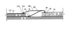
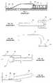
- FIG. 1is a diagrammatic sketch in an elevational view showing a semiconductor die affixed to a substrate, having conventional forward wire bond interconnection between the die and the substrate.
- FIG. 2Ais a diagrammatic sketch in a plan view of a portion of a conventional forward wire bond interconnection as in FIG. 1 , showing a conventional first bond of the wire to a pad on the die.
- FIG. 2Bis a diagrammatic sketch showing a conventional first bond as in FIG. 2A , in an elevational view.
- FIG. 3Ais a diagrammatic sketch in a plan view of a portion of a conventional forward wire bond interconnection as in FIG. 1 , showing a conventional second bond of the wire to a bond finger on the substrate.
- FIG. 3Bis a diagrammatic sketch showing a conventional second bond as in FIG. 3A , in an elevational view.
- FIG. 4is a diagrammatic sketch in an elevational view showing a semiconductor die affixed to a substrate, having conventional reverse wire bond interconnection between the die and the substrate.
- FIG. 5is a diagrammatic sketch in an elevational view showing a conventional second bond of the wire on a ball on the die pad.
- FIG. 6Ais a diagrammatic sketch in a plan view of a portion of a conventional forward wire bond interconnection as in FIG. 1 , showing a properly aligned second bond of the wire to a narrow bond finger on the substrate.
- FIG. 6Bis a diagrammatic sketch in a plan view of a portion of a conventional forward wire bond interconnection as in FIG. 1 , showing a misaligned second bond of the wire to a narrow bond finger on the substrate.
- FIG. 7Ais a diagrammatic sketch in a plan view of a portion of a forward wire bond interconnection to a narrow bond finger according to an embodiment of the invention, showing a second bond of the wire to a pedestal on a narrow bond finger on the substrate.
- FIG. 7Bis a diagrammatic sketch showing the second bond according to an embodiment of the invention as in FIG. 7A , in an elevational view.
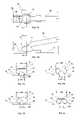
- FIG. 7Cis a diagrammatic sketch showing the second bond as in FIGS. 7A , 7 B in a sectional view at 7 C- 7 C.
- FIGS. 7D , 7 Eare diagrammatic sketches in sectional views generally as in FIG. 7C , showing various narrow bond finger configurations.
- FIG. 8is a diagrammatic sketch showing the second bond according to an embodiment of the invention, in a sectional view.
- FIGS. 9A , 9 Bare diagrammatic sketches in plan view each showing high density interconnection of a portion of a die to a portion of a substrate according to an embodiment of the invention.
- FIGS. 10A , 10 Bare diagrammatic sketches in a sectional view and in a plain view showing high density interconnection of a portion of a die to a portion of a tiered substrate according to an embodiment of the invention.
- FIGS. 11A-11Dare diagrammatic sketches in a sectional view showing steps in the formation of first (right in the FIGS.) and second (left in the FIGS.) interconnection of a die with a substrate according to an embodiment of the invention.
- FIG. 1there is shown a conventional wire bond interconnect.
- a semiconductor die 14is mounted active side upward upon a die attach surface of a substrate 12 and affixed there using a die attach adhesive 13 .
- the active side of the die 14is provided with interconnect pads 22 ; other features of the die are not shown in the FIGS.
- the substrateincludes at least one layer of a dielectric material and at least one patterned metal layer.
- a metal layer in the die attach side of the substrate 12is patterned to provide appropriate circuit traces, including bond fingers 32 .
- the die 14is electrically interconnected with the circuitry on the substrate by wires 26 formed between the die pads 24 and the bond fingers 32 .
- Wire bonding processesare well known. The following outline of an illustrative conventional wire bonding process is offered by way of example only.
- the wire bondis formed using machinery including a capillary bonding tool, a support for the device to be wire bonded, a source of heat, a source and transducer to impart ultrasound vibration to the capillary bonding tool, and means—typically at least partially automated, and at least partially under programmable computer control—for coordinating the movement of these machinery elements and the implementation of their functions.
- a wiretypically of aluminum or gold, is carried in the lumen of the capillary, and the machinery includes means for controlling the movement of the wire through the tip of the capillary. To form a wire bond as shown for example in FIG.
- the dieis affixed to the substrate, and then the die and substrate are mounted on the support stage.
- the supportis provided with a heater that controllably heats the substrate and die.
- the capillaryis poised over the die and substrate, and a wire is fed through the capillary lumen so that it projects to a selected extent from the capillary tip.
- the first bondis formed as follows: An electric arc is struck to form a molten ball at the projecting end of the wire.
- the capillarymoved over the die and substrate so that the tip is aligned in the x-y plane over the first target bonding site (the die pad in this example).
- Tensionis drawn on the wire to pull the ball back into a chamfer in the capillary tip as the capillary is lowered to bring the ball into contact with the first target bonding site.
- the capillaryis moved in the z direction to press the ball against the bonding site, and the transducer is activated to impart an ultrasonic vibration to the capillary.
- the capillary tip(particularly, the chamfer, which grips the ball at this phase) imparts a vibration to the ball as it is compressed against the target.
- a metallurgic bondis formed between the ball and the target, completing first bond (the “ball” bond).
- the wire “loop”is formed as follows: the wire is fed through the capillary is the capillary is raised away from the first target, and then moved in a controlled path in relation to the die and substrate (to control the eventual shape of the completed wire bond) toward a position where it is aligned in the x-y plane over the second target bonding site (a pad or bond finger on a trace on the substrate in this example).
- the second bondis formed as follows: The capillary is lowered to press the wire against the second target bonding site, and again the transducer is activated to impart a vibration to the wire as it is squashed against the target, forming a metallurgic bond between the wire and the target.
- the capillaryis moved along the bond site, and is then raised, forming a “tail” of wire projecting from the capillary tip. Finally, the wire is gripped as the capillary is raised further, causing the wire to break near the second bond and leaving the “tail” of wire projecting from the capillary tip, ready for formation of a subsequent ball by electric arc at the wire end.
- the appearance of an illustrative first (“ball”) bondis shown diagrammatically in two views at FIGS. 2A and 2B
- the appearance of an illustrative second (“stitch”) bondis shown diagrammatically in two views at FIGS. 3A and 3B
- the completed ball bondincludes a compressed ball 24 metallurgically bonded to the die pad 22
- the completed stitch bondincludes a squashed wire end 34 metallurgically bonded to a “flat” or “pad” on the bond finger 32 . A residue of the wire can remain in place on the pad, as indicated at 35 .
- first and second bondswill be expected, depending on other things upon the shape and dimensions of the capillary tip (particularly the chamfer) and upon various other process parameters.
- some variation in the appearance of the second bondmay result from the use of given machinery and processing parameters, owing to the fact that the wire is broken to complete the bond.
- the bond finger or bond padtypically has at the bond site a generally flat “landing” surface, sometimes termed a “flat”, on which the bond is formed, which is significantly wider than the completed stitch bond formed upon it, as discussed above.
- a reverse wire bonding processthe first (“ball”) bond is formed on the lead finger flat or pad, and the second (“stitch”) bond is formed on the die pad. It may be advisable where a reverse wire bonding process connects a substrate with a die, to raise the second end of the wire, near the second bond, to avoid contact of the wire with the active surface of the die. Accordingly in a reverse wire bonding process a ball may be formed on the die pad, upon which the second (“stitch”) bond is formed. Such a procedure is shown, for example, in Lee U.S. Pat. No. 6,561,411.
- FIG. 4An illustrative example of such a reverse wire bond interconnect is shown by way of example in FIG. 4 .
- a semiconductor die 14is mounted active side upward upon a die attach surface of a substrate 12 and affixed there using a die attach adhesive 13 .
- the active side of the die 14is provided with interconnect pads 22 ; other features of the die are not shown in the FIGS.
- the substrateincludes at least one layer of a dielectric material and at least one patterned metal layer.
- a metal layer in the die attach side of the substrate 12is patterned to provide appropriate circuit traces, including bond fingers 32 .
- the die 14is electrically interconnected with the circuitry on the substrate by wires 26 formed between the die pads 24 and the bond fingers 32 .
- the first (“ball”) bond 24is formed on a “flat” or “pad” of the bond finger 32 and the second (“stitch”) bond 54 is formed on a pedestal 56 formed as a ball previously deposited on the die pad 22 .
- a diagrammatic illustration of a second (“stitch”) bond 54 on a ball 56 on a die pad 22is illustrated by way of example in FIG. 5 .
- the stitch bondmay be acceptably robust.
- there may be a sufficiently good metallurgic bond between the portion 64 of the second wire end 66 and the narrow bond finger 62although this may depend upon the extent to which the flattened remnant of the flattened wire outlined by broken line 65 , whose form may be unreliable, may aid in providing a good conductive interconnection.
- the second bonding processcan fail to make a good connection with the bond finger 62 . It is uncertain what the configuration of the resulting portion 66 of the wire end 66 and of the residue 65 of the second bonding process may be, but, in any event, a consistently or reliable or robust bond cannot be suitably assured. Accordingly, trying to reduce lead finger pitch by narrowing the flat width on the lead finger is generally not acceptable.
- the bond fingeris narrow at the second bond site, a pedestal is formed on the narrow bond site, and the second (“stitch”) bond is formed on the pedestal.
- the pedestalcan be formed as a ball, for example, in the manner of forming a stud bump. That is, wire bonding apparatus is employed to form a ball on the narrow bond finger as if forming a first (“ball”) bond interconnection, but then, instead of drawing the wire to form a loop, the wire is clamped as the capillary is moved upward, so that the wire breaks off just above the ball, leaving a “tail”.
- the top of the ball, including the wire tail,may be flattened, for example by “coining”, to form a generally flattened surface before the second (“stitch”) bond is formed on it.
- the stitch bondis formed generally as described above with reference to FIGS. 3A , 3 B, except that here the stitch bond is formed upon the (usually flattened) surface of the pedestal 72 rather than on the flat landing surface of the bond finger 32 .
- the completed stitch bondincludes a squashed wire end 74 metallurgically bonded to the pedestal 72 , and a residue of the wire can remain in place on the pad, as indicated at 75 .
- first and second bondsSome variation in the shapes of the first and second bonds will be expected, depending on other things upon the shape and dimensions of the capillary tip (particularly the chamfer) and upon various other process parameters. Particularly, some variation in the appearance of the second bond may result from the use of given machinery and processing parameters, owing to the fact that the wire is broken to complete the bond.
- a resulting second bond according to the inventionis shown by way of example in FIGS. 7A , 7 B.
- a narrow bond site 62 on a lead fingerhas a generally trapezoidal, or roughly triangular (truncated), or roughly triangular (with a rounded apex) cross section (refer to FIGS. 7C-7E ).
- the bond site part 62 of the lead fingerhas a generally trapezoidal cross section, with a roughly flat top
- the width WP of the flat top 71 of the bond finger at the bond siteis less than the width (roughly, the diameter) WB of the support pedestal 72 .
- the width WF of the base 73 of the bond finger at the bond sitewhich is somewhat larger than the width WP of the flat top 71 , is also less than the width (diameter) WB of the support pedestal 72 .
- the top 71 of the bond site part of the bond fingeris not perfectly flat and the edges of it are not as sharply defined as appears in the FIGS.
- the top 77 of the bond site part of the bond fingermay be rounded.
- the top of the bond site part of the bond fingeris narrower than the pedestal diameter, and the process of forming the support pedestal 72 on the bond site part of the bond finger causes the ball to deform around the lead finder at the bond site.
- the bond fingermay be made proportionately much narrower than the pedestal diameter WB and, as illustrated in FIG. 7E , the bond finger at the bond site may be narrowed so that the cross sectional shape is nearly triangular, as illustrated for example in FIG. 7E , with an apex 79 , which has no flat but may be rounded.
- FIGS. 7C-7Eshow, whether the lead finger at the bond site has a generally flat ( FIG. 7A ) or rounded ( FIG. 7B ) plateau, or has sharp or rounded apex ( FIG.
- the support pedestal 72conforms to the shape of the plateau or apex; that is, as the support pedestal is formed, it conforms to at least the upper part of at least one of the sides of the lead finger.
- the support pedestalwas precisely aligned with the bond site during its formation, so that it is symmetrically disposed upon the lead finger and, accordingly, parts of the pedestal have been equally deformed one the two sides of the lead finger. It is not necessary that the support pedestal be perfectly aligned, and in practice the deformation may be asymmetrical to some extent. Moreover, as illustrated for example in FIG.
- parts of the support pedestal 82may touch the surface of the substrate 12 alongside the base of the lead finger 63 .
- a second (“stitch”) bond 75can be reliably formed upon a support pedestal 72 , 82 so formed, as illustrated in FIGS. 7C-7E and 8 .
- the feature widthmay vary among the various leads and lead fingers on the substrate, and may vary along the length of a given lead or lead finger according to the invention, the lead finger (at least the plateau of the lead finger) is less than the support pedestal diameter at the bond site, that is, at the place along the length of the lead where the support pedestal is formed; the trace may be narrower or wider at other points, so long as the desired lead finger density (and lead finger bond pitch) is obtained.
- FIGS. 9A and 9Bshow in plan view two lead finger arrangements according to the invention in which the die pad pitch PDP is the same as the lead finger bond pitch PLF, so that the wires run parallel, rather than fanning out, as they must where the lead finger bond pitch is greater than the die pad pitch.
- Die pads 22are arrayed in a row along an edge 15 of the die 14 .
- Lead fingers 62narrowed at the bond sites, are arranged in the die attach surface of the substrate 12 in a row, with the bond fingers generally aligned with the corresponding die pads.
- FIG. 9Bis formed at the lead finger bond site on each lead finger; in FIG. 7A the support pedestals are arranged in a single line, while in FIG. 7B they are arranged in two staggered rows.
- the arrangement of FIG. 7Bprovides a greater distance between nearest support pedestals while maintaining the same pitch (die pad pitch PDP′; lead finger bond pitch PLF′).
- wire bondsare formed between the die pads and the respective bond fingers, by forming a first (“ball”) bond 24 on the die pad 22 , drawing the wire 66 ( 66 ′) to the respective lead finger 62 ( 62 ′) bond site, and forming a second (“stitch”) bond 74 ( 74 ′) on the support pedestal 72 ( 72 ′), as described for example with reference to FIGS. 7A-7E and 8 .
- die padsare arranged in a row along an edge of the die 14 .
- Lead fingers having narrow bond sites 162are arranged in the die attach surface of a first (lower) substrate 12 in a first row, with the lead fingers generally aligned with corresponding alternating ones (1 st , 3 rd , 5 th , etc.) of the die pads; and lead fingers having narrow bond sites 162 ′ are arranged in a surface of a second (upper) substrate 112 in a second row, with the lead fingers generally aligned with alternating ones (2 nd , 4 th , 6 th , etc.) of the die pads not corresponding lead fingers in the first substrate.
- the edge of the upper substrateis set back so that the bond sites on the lead fingers on the lower substrate are exposed.
- a first row of support pedestals 72are formed at the exposed lead finger bond sites of the lead fingers 71 on the lower substrate 12
- a second row of support pedestals 172are formed at the lead finger bond sites of the lead fingers 171 on the upper substrate 112 .
- Wire bondsare formed between the die pads 22 and the respective bond fingers, alternately 71 , 171 , by forming a first (“ball”) bond 24 on the die pad 22 , drawing the wire 66 , 166 to the respective lead finger 71 , 171 bond site, and forming a second (“stitch”) bond 74 , 174 on the support pedestal 72 , 172 , as described for example with reference to FIGS. 7A-7E and 8 .
- the lead finger bond pitch PLF′′ in both the lower and the upper rows of lead fingersis twice as great as the die pad pitch PDP′.
- a fine lead finger bond pitch(for example, in a range between about 80 ⁇ m and about 100 ⁇ m can be obtained in each of the rows of lead fingers, and because the lead fingers in the two rows are staggered, the combined effective lead finger bond pitch is half as great as in each row (that is, in the example given above, between about 40 ⁇ m and about 50 ⁇ m).
- Thiscan provide for orthogonal wire bond interconnection of a die having a pad pitch in a range as small as about 40 ⁇ m and about 50 ⁇ m, and wire lengths as short as 1 mm or shorter can be possible.
- FIGS. 11A-11DStages in a generalized process for making a wire bind interconnect according to the inventions are illustrated in FIGS. 11A-11D .
- FIG. 11Ashows a stage in which a die 22 mounted using a die attach adhesive 13 on a die attach side of a substrate 12 is provided. Electrical interconnect pads 22 are situated in the active side of the die. Lead fingers having narrow bond sites 62 are patterned in a metal layer in the substrate.
- a ball 272is formed by a stud bumping procedure on the bond site of the lead finger 62 , as shown in FIG. 11B .
- the ballis then flattened, for example by coining, to form a support pedestal 72 at the bond site on the lead finger as shown in FIG. 11C .
- a ball bond 24is formed on the die pad 22 , the wire 26 is drawn to the bond site on the lead finger 62 , and a stitch bond 74 is formed on the support pedestal 72 .
- Other stepswill be interposed or added, including steps well known in the art. For example, following wire bonding of all the appropriate die pads with all the corresponding lead fingers, the die and wires are molded or encapsulated.
Landscapes
- Engineering & Computer Science (AREA)
- Computer Hardware Design (AREA)
- Microelectronics & Electronic Packaging (AREA)
- Power Engineering (AREA)
- Physics & Mathematics (AREA)
- Condensed Matter Physics & Semiconductors (AREA)
- General Physics & Mathematics (AREA)
- Wire Bonding (AREA)
- Lead Frames For Integrated Circuits (AREA)
Abstract
Description
Claims (22)
Priority Applications (6)
| Application Number | Priority Date | Filing Date | Title |
|---|---|---|---|
| US11/273,635US7453156B2 (en) | 2004-11-12 | 2005-11-14 | Wire bond interconnection |
| US11/839,020US7868468B2 (en) | 2004-11-12 | 2007-08-15 | Wire bonding structure and method that eliminates special wire bondable finish and reduces bonding pitch on substrates |
| US12/032,159US7745322B2 (en) | 2004-11-12 | 2008-02-15 | Wire bond interconnection |
| US12/783,039US7986047B2 (en) | 2004-11-12 | 2010-05-19 | Wire bond interconnection |
| US12/973,410US8269356B2 (en) | 2004-11-12 | 2010-12-20 | Wire bonding structure and method that eliminates special wire bondable finish and reduces bonding pitch on substrates |
| US13/178,331US8129263B2 (en) | 2004-11-12 | 2011-07-07 | Wire bond interconnection and method of manufacture thereof |
Applications Claiming Priority (2)
| Application Number | Priority Date | Filing Date | Title |
|---|---|---|---|
| US62765004P | 2004-11-12 | 2004-11-12 | |
| US11/273,635US7453156B2 (en) | 2004-11-12 | 2005-11-14 | Wire bond interconnection |
Related Child Applications (2)
| Application Number | Title | Priority Date | Filing Date |
|---|---|---|---|
| US11/839,020Continuation-In-PartUS7868468B2 (en) | 2004-11-12 | 2007-08-15 | Wire bonding structure and method that eliminates special wire bondable finish and reduces bonding pitch on substrates |
| US12/032,159DivisionUS7745322B2 (en) | 2004-11-12 | 2008-02-15 | Wire bond interconnection |
Publications (2)
| Publication Number | Publication Date |
|---|---|
| US20060113665A1 US20060113665A1 (en) | 2006-06-01 |
| US7453156B2true US7453156B2 (en) | 2008-11-18 |
Family
ID=36337287
Family Applications (4)
| Application Number | Title | Priority Date | Filing Date |
|---|---|---|---|
| US11/273,635Active2026-05-02US7453156B2 (en) | 2004-11-12 | 2005-11-14 | Wire bond interconnection |
| US12/032,159ActiveUS7745322B2 (en) | 2004-11-12 | 2008-02-15 | Wire bond interconnection |
| US12/783,039ActiveUS7986047B2 (en) | 2004-11-12 | 2010-05-19 | Wire bond interconnection |
| US13/178,331ActiveUS8129263B2 (en) | 2004-11-12 | 2011-07-07 | Wire bond interconnection and method of manufacture thereof |
Family Applications After (3)
| Application Number | Title | Priority Date | Filing Date |
|---|---|---|---|
| US12/032,159ActiveUS7745322B2 (en) | 2004-11-12 | 2008-02-15 | Wire bond interconnection |
| US12/783,039ActiveUS7986047B2 (en) | 2004-11-12 | 2010-05-19 | Wire bond interconnection |
| US13/178,331ActiveUS8129263B2 (en) | 2004-11-12 | 2011-07-07 | Wire bond interconnection and method of manufacture thereof |
Country Status (5)
| Country | Link |
|---|---|
| US (4) | US7453156B2 (en) |
| JP (1) | JP4964780B2 (en) |
| KR (1) | KR101227228B1 (en) |
| TW (1) | TWI368974B (en) |
| WO (1) | WO2006053277A2 (en) |
Cited By (5)
| Publication number | Priority date | Publication date | Assignee | Title |
|---|---|---|---|---|
| US20060266804A1 (en)* | 2005-05-17 | 2006-11-30 | Wang Chin S | Chip package and wire bonding process thereof |
| US20090032932A1 (en)* | 2007-08-03 | 2009-02-05 | Byung Tai Do | Integrated circuit packaging system for fine pitch substrates |
| US20110221058A1 (en)* | 2010-03-09 | 2011-09-15 | Stats Chippac, Ltd. | Semiconductor device and method of forming vertically offset bond on trace interconnects on different height traces |
| US8409978B2 (en) | 2010-06-24 | 2013-04-02 | Stats Chippac, Ltd. | Semiconductor device and method of forming vertically offset bond on trace interconnect structure on leadframe |
| US10600756B1 (en) | 2017-02-15 | 2020-03-24 | United States Of America, As Represented By The Secretary Of The Navy | Wire bonding technique for integrated circuit board connections |
Families Citing this family (28)
| Publication number | Priority date | Publication date | Assignee | Title |
|---|---|---|---|---|
| US7868468B2 (en)* | 2004-11-12 | 2011-01-11 | Stats Chippac Ltd. | Wire bonding structure and method that eliminates special wire bondable finish and reduces bonding pitch on substrates |
| JP4964780B2 (en)* | 2004-11-12 | 2012-07-04 | スタッツ・チップパック・インコーポレイテッド | Wire bond interconnect, semiconductor package, and method of forming wire bond interconnect |
| US7731078B2 (en)* | 2004-11-13 | 2010-06-08 | Stats Chippac Ltd. | Semiconductor system with fine pitch lead fingers |
| US8519517B2 (en)* | 2004-11-13 | 2013-08-27 | Stats Chippac Ltd. | Semiconductor system with fine pitch lead fingers and method of manufacturing thereof |
| EP3479844B1 (en) | 2005-04-15 | 2023-11-22 | MacroGenics, Inc. | Covalent diabodies and uses thereof |
| US20070018292A1 (en)* | 2005-07-22 | 2007-01-25 | Sehat Sutardja | Packaging for high speed integrated circuits |
| US20070026573A1 (en)* | 2005-07-28 | 2007-02-01 | Aminuddin Ismail | Method of making a stacked die package |
| US7863099B2 (en)* | 2007-06-27 | 2011-01-04 | Stats Chippac Ltd. | Integrated circuit package system with overhanging connection stack |
| SG148901A1 (en) | 2007-07-09 | 2009-01-29 | Micron Technology Inc | Packaged semiconductor assemblies and methods for manufacturing such assemblies |
| US20090243051A1 (en)* | 2008-03-28 | 2009-10-01 | Micron Technology, Inc. | Integrated conductive shield for microelectronic device assemblies and associated methods |
| US7897502B2 (en)* | 2008-09-10 | 2011-03-01 | Stats Chippac, Ltd. | Method of forming vertically offset bond on trace interconnects on recessed and raised bond fingers |
| US7973394B2 (en)* | 2009-06-10 | 2011-07-05 | Blondwich Limited | Enhanced integrated circuit package |
| CN102511082B (en)* | 2009-09-16 | 2016-04-27 | 株式会社半导体能源研究所 | Semiconductor device and manufacturing method thereof |
| US8304921B2 (en)* | 2009-11-13 | 2012-11-06 | Stats Chippac Ltd. | Integrated circuit packaging system with interconnect and method of manufacture thereof |
| US8609525B2 (en)* | 2011-03-21 | 2013-12-17 | Stats Chippac Ltd. | Integrated circuit packaging system with interconnects and method of manufacture thereof |
| JP5990897B2 (en) | 2011-11-25 | 2016-09-14 | ソニー株式会社 | Power control device, power transmission device, and power control system |
| US8643159B2 (en) | 2012-04-09 | 2014-02-04 | Freescale Semiconductor, Inc. | Lead frame with grooved lead finger |
| JP2013229368A (en)* | 2012-04-24 | 2013-11-07 | Denso Corp | Electronic device and manufacturing method of the same |
| JP5894502B2 (en)* | 2012-06-04 | 2016-03-30 | ローム株式会社 | Wire bonding structure and semiconductor device |
| US9837188B2 (en)* | 2012-07-06 | 2017-12-05 | Nxp B.V. | Differential return loss supporting high speed bus interfaces |
| US20150206830A1 (en)* | 2012-09-24 | 2015-07-23 | Renesas Electronics Corporation | Method Of Manufacturing Semiconductor Device And The Semiconductor Device |
| US8680660B1 (en) | 2013-03-12 | 2014-03-25 | Freescale Semiconductor, Inc. | Brace for bond wire |
| US20140312474A1 (en)* | 2013-04-19 | 2014-10-23 | Texas Instruments Incorporated | Semiconductor package with wire bonding |
| KR101563911B1 (en)* | 2013-10-24 | 2015-10-28 | 앰코 테크놀로지 코리아 주식회사 | Semiconductor package |
| JP6279339B2 (en)* | 2014-02-07 | 2018-02-14 | ルネサスエレクトロニクス株式会社 | Manufacturing method of semiconductor device |
| US9881870B2 (en)* | 2015-12-30 | 2018-01-30 | Taiwan Semiconductor Manufacturing Co., Ltd. | Semiconductor device and manufacturing method thereof |
| CA3143350A1 (en) | 2019-05-31 | 2020-12-03 | Janssen Pharmaceutica Nv | Small molecule inhibitors of nf-kb inducing kinase |
| GB2621374A (en) | 2022-08-10 | 2024-02-14 | Toshiba Kk | An electronic package and method of manufacturing an electronic package |
Citations (27)
| Publication number | Priority date | Publication date | Assignee | Title |
|---|---|---|---|---|
| US4742023A (en)* | 1986-08-28 | 1988-05-03 | Fujitsu Limited | Method for producing a semiconductor device |
| US5329157A (en) | 1992-07-17 | 1994-07-12 | Lsi Logic Corporation | Semiconductor packaging technique yielding increased inner lead count for a given die-receiving area |
| US5328079A (en) | 1993-03-19 | 1994-07-12 | National Semiconductor Corporation | Method of and arrangement for bond wire connecting together certain integrated circuit components |
| US5340770A (en) | 1992-10-23 | 1994-08-23 | Ncr Corporation | Method of making a shallow junction by using first and second SOG layers |
| US5444303A (en) | 1994-08-10 | 1995-08-22 | Motorola, Inc. | Wire bond pad arrangement having improved pad density |
| US5465899A (en) | 1994-10-14 | 1995-11-14 | Texas Instruments Incorporated | Method and apparatus for fine pitch wire bonding using a shaved capillary |
| US5561086A (en) | 1993-06-18 | 1996-10-01 | Lsi Logic Corporation | Techniques for mounting semiconductor dies in die-receiving areas having support structure having notches |
| US5654585A (en)* | 1994-09-30 | 1997-08-05 | Nec Corporation | Semiconductor device with at least one lead having a plurality of bent portions |
| US5686762A (en)* | 1995-12-21 | 1997-11-11 | Micron Technology, Inc. | Semiconductor device with improved bond pads |
| US5904288A (en) | 1996-04-08 | 1999-05-18 | Texas Instruments Incorporated | Wire bond clamping method |
| US5960262A (en) | 1997-09-26 | 1999-09-28 | Texas Instruments Incorporated | Stitch bond enhancement for hard-to-bond materials |
| US5994169A (en) | 1994-10-27 | 1999-11-30 | Texas Instruments Incorporated | Lead frame for integrated circuits and process of packaging |
| US6158647A (en) | 1998-09-29 | 2000-12-12 | Micron Technology, Inc. | Concave face wire bond capillary |
| US6294830B1 (en)* | 1996-04-18 | 2001-09-25 | Tessera, Inc. | Microelectronic assembly with conductive terminals having an exposed surface through a dielectric layer |
| US6329278B1 (en) | 2000-01-03 | 2001-12-11 | Lsi Logic Corporation | Multiple row wire bonding with ball bonds of outer bond pads bonded on the leads |
| US6462414B1 (en)* | 1999-03-05 | 2002-10-08 | Altera Corporation | Integrated circuit package utilizing a conductive structure for interlocking a conductive ball to a ball pad |
| US6541848B2 (en) | 1998-02-25 | 2003-04-01 | Fujitsu Limited | Semiconductor device including stud bumps as external connection terminals |
| US6561411B2 (en) | 2000-12-22 | 2003-05-13 | Advanced Semiconductor Engineering, Inc. | Wire bonding process and wire bond structure |
| US20030089521A1 (en) | 2001-11-13 | 2003-05-15 | Lg Electronics Inc. | Bonding pad(s) for a printed circuit board and a method for forming bonding pad(s) |
| US6624059B2 (en) | 1997-04-22 | 2003-09-23 | Micron Technology, Inc. | Method of improving interconnect of semiconductor devices by utilizing a flattened ball bond |
| US6713881B2 (en) | 2000-05-29 | 2004-03-30 | Texas Instruments Incorporated | Semiconductor device and method of manufacturing same |
| US20040152292A1 (en)* | 2002-09-19 | 2004-08-05 | Stephen Babinetz | Method and apparatus for forming bumps for semiconductor interconnections using a wire bonding machine |
| US6787926B2 (en)* | 2001-09-05 | 2004-09-07 | Taiwan Semiconductor Manufacturing Co., Ltd | Wire stitch bond on an integrated circuit bond pad and method of making the same |
| US6849931B2 (en) | 2001-06-11 | 2005-02-01 | Rohm Co., Ltd. | Lead frame |
| US20050133928A1 (en)* | 2003-12-19 | 2005-06-23 | Howard Gregory E. | Wire loop grid array package |
| US20060049523A1 (en) | 2004-09-07 | 2006-03-09 | Advanced Semiconductor Engineering, Inc. | Wire-bonding method for connecting wire-bond pads and chip and the structure formed thereby |
| US20060102694A1 (en) | 2004-11-13 | 2006-05-18 | Stats Chippac Ltd. | Semiconductor system with fine pitch lead fingers |
Family Cites Families (29)
| Publication number | Priority date | Publication date | Assignee | Title |
|---|---|---|---|---|
| JPS5933894A (en) | 1982-08-19 | 1984-02-23 | 電気化学工業株式会社 | Method of producing hybrid integrated circuit board |
| US5007576A (en) | 1989-12-26 | 1991-04-16 | Hughes Aircraft Company | Testable ribbon bonding method and wedge bonding tool for microcircuit device fabrication |
| US5158647A (en)* | 1991-01-10 | 1992-10-27 | Raymond Hurley | Capacitor papers of flash-spun synthetic pulp fibers |
| JP2601666Y2 (en) | 1992-05-08 | 1999-11-29 | 株式会社村田製作所 | Laminated coil |
| US5480834A (en) | 1993-12-13 | 1996-01-02 | Micron Communications, Inc. | Process of manufacturing an electrical bonding interconnect having a metal bond pad portion and having a conductive epoxy portion comprising an oxide reducing agent |
| KR0130534B1 (en)* | 1994-07-12 | 1998-04-09 | 김광호 | Linear motor for a washing machine |
| US5842628A (en)* | 1995-04-10 | 1998-12-01 | Fujitsu Limited | Wire bonding method, semiconductor device, capillary for wire bonding and ball bump forming method |
| JPH0982742A (en)* | 1995-09-11 | 1997-03-28 | Fujitsu Ltd | Wire bonding method |
| US5734559A (en)* | 1996-03-29 | 1998-03-31 | Intel Corporation | Staggered bond finger design for fine pitch integrated circuit packages |
| US5735030A (en)* | 1996-06-04 | 1998-04-07 | Texas Instruments Incorporated | Low loop wire bonding |
| JP3022819B2 (en)* | 1997-08-27 | 2000-03-21 | 日本電気アイシーマイコンシステム株式会社 | Semiconductor integrated circuit device |
| EP0903780A3 (en)* | 1997-09-19 | 1999-08-25 | Texas Instruments Incorporated | Method and apparatus for a wire bonded package for integrated circuits |
| US6008532A (en)* | 1997-10-23 | 1999-12-28 | Lsi Logic Corporation | Integrated circuit package having bond fingers with alternate bonding areas |
| US6064113A (en)* | 1998-01-13 | 2000-05-16 | Lsi Logic Corporation | Semiconductor device package including a substrate having bonding fingers within an electrically conductive ring surrounding a die area and a combined power and ground plane to stabilize signal path impedances |
| TW410446B (en)* | 1999-01-21 | 2000-11-01 | Siliconware Precision Industries Co Ltd | BGA semiconductor package |
| US6333562B1 (en)* | 2000-07-13 | 2001-12-25 | Advanced Semiconductor Engineering, Inc. | Multichip module having stacked chip arrangement |
| EP1198004A3 (en)* | 2000-10-13 | 2003-10-01 | Texas Instruments Inc. | Semiconductor device having power distribution lines thereon |
| US7135759B2 (en)* | 2000-10-27 | 2006-11-14 | Texas Instruments Incorporated | Individualized low parasitic power distribution lines deposited over active integrated circuits |
| US6597065B1 (en)* | 2000-11-03 | 2003-07-22 | Texas Instruments Incorporated | Thermally enhanced semiconductor chip having integrated bonds over active circuits |
| TW495940B (en)* | 2001-07-20 | 2002-07-21 | Via Tech Inc | Method for forming a grid array packaged integrated circuit |
| US7190060B1 (en) | 2002-01-09 | 2007-03-13 | Bridge Semiconductor Corporation | Three-dimensional stacked semiconductor package device with bent and flat leads and method of making same |
| JP3824545B2 (en)* | 2002-02-07 | 2006-09-20 | 松下電器産業株式会社 | Wiring board, semiconductor device using the same, and manufacturing method thereof |
| US6815836B2 (en)* | 2003-03-24 | 2004-11-09 | Texas Instruments Incorporated | Wire bonding for thin semiconductor package |
| US6927479B2 (en)* | 2003-06-25 | 2005-08-09 | St Assembly Test Services Ltd | Method of manufacturing a semiconductor package for a die larger than a die pad |
| US6956286B2 (en)* | 2003-08-05 | 2005-10-18 | International Business Machines Corporation | Integrated circuit package with overlapping bond fingers |
| US7375978B2 (en)* | 2003-12-23 | 2008-05-20 | Intel Corporation | Method and apparatus for trace shielding and routing on a substrate |
| KR100604840B1 (en)* | 2004-03-11 | 2006-07-28 | 삼성전자주식회사 | Reverse wire bonding method to fine pitch bumps and wire bond structure thereby |
| JP4964780B2 (en)* | 2004-11-12 | 2012-07-04 | スタッツ・チップパック・インコーポレイテッド | Wire bond interconnect, semiconductor package, and method of forming wire bond interconnect |
| US7358617B2 (en)* | 2004-11-29 | 2008-04-15 | Texas Instruments Incorporated | Bond pad for ball grid array package |
- 2005
- 2005-11-14JPJP2007541391Apatent/JP4964780B2/enactiveActive
- 2005-11-14KRKR1020077010429Apatent/KR101227228B1/enactiveActive
- 2005-11-14WOPCT/US2005/041116patent/WO2006053277A2/enactiveApplication Filing
- 2005-11-14USUS11/273,635patent/US7453156B2/enactiveActive
- 2005-11-14TWTW094139959Apatent/TWI368974B/enactive
- 2008
- 2008-02-15USUS12/032,159patent/US7745322B2/enactiveActive
- 2010
- 2010-05-19USUS12/783,039patent/US7986047B2/enactiveActive
- 2011
- 2011-07-07USUS13/178,331patent/US8129263B2/enactiveActive
Patent Citations (27)
| Publication number | Priority date | Publication date | Assignee | Title |
|---|---|---|---|---|
| US4742023A (en)* | 1986-08-28 | 1988-05-03 | Fujitsu Limited | Method for producing a semiconductor device |
| US5329157A (en) | 1992-07-17 | 1994-07-12 | Lsi Logic Corporation | Semiconductor packaging technique yielding increased inner lead count for a given die-receiving area |
| US5340770A (en) | 1992-10-23 | 1994-08-23 | Ncr Corporation | Method of making a shallow junction by using first and second SOG layers |
| US5328079A (en) | 1993-03-19 | 1994-07-12 | National Semiconductor Corporation | Method of and arrangement for bond wire connecting together certain integrated circuit components |
| US5561086A (en) | 1993-06-18 | 1996-10-01 | Lsi Logic Corporation | Techniques for mounting semiconductor dies in die-receiving areas having support structure having notches |
| US5444303A (en) | 1994-08-10 | 1995-08-22 | Motorola, Inc. | Wire bond pad arrangement having improved pad density |
| US5654585A (en)* | 1994-09-30 | 1997-08-05 | Nec Corporation | Semiconductor device with at least one lead having a plurality of bent portions |
| US5465899A (en) | 1994-10-14 | 1995-11-14 | Texas Instruments Incorporated | Method and apparatus for fine pitch wire bonding using a shaved capillary |
| US5994169A (en) | 1994-10-27 | 1999-11-30 | Texas Instruments Incorporated | Lead frame for integrated circuits and process of packaging |
| US5686762A (en)* | 1995-12-21 | 1997-11-11 | Micron Technology, Inc. | Semiconductor device with improved bond pads |
| US5904288A (en) | 1996-04-08 | 1999-05-18 | Texas Instruments Incorporated | Wire bond clamping method |
| US6294830B1 (en)* | 1996-04-18 | 2001-09-25 | Tessera, Inc. | Microelectronic assembly with conductive terminals having an exposed surface through a dielectric layer |
| US6624059B2 (en) | 1997-04-22 | 2003-09-23 | Micron Technology, Inc. | Method of improving interconnect of semiconductor devices by utilizing a flattened ball bond |
| US5960262A (en) | 1997-09-26 | 1999-09-28 | Texas Instruments Incorporated | Stitch bond enhancement for hard-to-bond materials |
| US6541848B2 (en) | 1998-02-25 | 2003-04-01 | Fujitsu Limited | Semiconductor device including stud bumps as external connection terminals |
| US6158647A (en) | 1998-09-29 | 2000-12-12 | Micron Technology, Inc. | Concave face wire bond capillary |
| US6462414B1 (en)* | 1999-03-05 | 2002-10-08 | Altera Corporation | Integrated circuit package utilizing a conductive structure for interlocking a conductive ball to a ball pad |
| US6329278B1 (en) | 2000-01-03 | 2001-12-11 | Lsi Logic Corporation | Multiple row wire bonding with ball bonds of outer bond pads bonded on the leads |
| US6713881B2 (en) | 2000-05-29 | 2004-03-30 | Texas Instruments Incorporated | Semiconductor device and method of manufacturing same |
| US6561411B2 (en) | 2000-12-22 | 2003-05-13 | Advanced Semiconductor Engineering, Inc. | Wire bonding process and wire bond structure |
| US6849931B2 (en) | 2001-06-11 | 2005-02-01 | Rohm Co., Ltd. | Lead frame |
| US6787926B2 (en)* | 2001-09-05 | 2004-09-07 | Taiwan Semiconductor Manufacturing Co., Ltd | Wire stitch bond on an integrated circuit bond pad and method of making the same |
| US20030089521A1 (en) | 2001-11-13 | 2003-05-15 | Lg Electronics Inc. | Bonding pad(s) for a printed circuit board and a method for forming bonding pad(s) |
| US20040152292A1 (en)* | 2002-09-19 | 2004-08-05 | Stephen Babinetz | Method and apparatus for forming bumps for semiconductor interconnections using a wire bonding machine |
| US20050133928A1 (en)* | 2003-12-19 | 2005-06-23 | Howard Gregory E. | Wire loop grid array package |
| US20060049523A1 (en) | 2004-09-07 | 2006-03-09 | Advanced Semiconductor Engineering, Inc. | Wire-bonding method for connecting wire-bond pads and chip and the structure formed thereby |
| US20060102694A1 (en) | 2004-11-13 | 2006-05-18 | Stats Chippac Ltd. | Semiconductor system with fine pitch lead fingers |
Non-Patent Citations (1)
| Title |
|---|
| International Search Report and Written Opinion for corresponding International Application No. PCT/US05/41116 dated May 07, 2007. |
Cited By (11)
| Publication number | Priority date | Publication date | Assignee | Title |
|---|---|---|---|---|
| US20060266804A1 (en)* | 2005-05-17 | 2006-11-30 | Wang Chin S | Chip package and wire bonding process thereof |
| US20090032932A1 (en)* | 2007-08-03 | 2009-02-05 | Byung Tai Do | Integrated circuit packaging system for fine pitch substrates |
| US7701049B2 (en) | 2007-08-03 | 2010-04-20 | Stats Chippac Ltd. | Integrated circuit packaging system for fine pitch substrates |
| US20100155926A1 (en)* | 2007-08-03 | 2010-06-24 | Byung Tai Do | Integrated circuit packaging system for fine pitch substrates and method of manufacture thereof |
| US8143107B2 (en) | 2007-08-03 | 2012-03-27 | Stats Chippac Ltd. | Integrated circuit packaging system substrates and method of manufacture thereof |
| US20110221058A1 (en)* | 2010-03-09 | 2011-09-15 | Stats Chippac, Ltd. | Semiconductor device and method of forming vertically offset bond on trace interconnects on different height traces |
| US8039384B2 (en) | 2010-03-09 | 2011-10-18 | Stats Chippac, Ltd. | Semiconductor device and method of forming vertically offset bond on trace interconnects on different height traces |
| US8563418B2 (en) | 2010-03-09 | 2013-10-22 | Stats Chippac, Ltd. | Semiconductor device and method of forming vertically offset bond on trace interconnects on different height traces |
| US8409978B2 (en) | 2010-06-24 | 2013-04-02 | Stats Chippac, Ltd. | Semiconductor device and method of forming vertically offset bond on trace interconnect structure on leadframe |
| US9236332B2 (en) | 2010-06-24 | 2016-01-12 | Stats Chippac, Ltd. | Semiconductor device and method of forming vertically offset bond on trace interconnect structure on leadframe |
| US10600756B1 (en) | 2017-02-15 | 2020-03-24 | United States Of America, As Represented By The Secretary Of The Navy | Wire bonding technique for integrated circuit board connections |
Also Published As
| Publication number | Publication date |
|---|---|
| US8129263B2 (en) | 2012-03-06 |
| US20080135997A1 (en) | 2008-06-12 |
| TWI368974B (en) | 2012-07-21 |
| JP2008520111A (en) | 2008-06-12 |
| KR101227228B1 (en) | 2013-01-28 |
| US20060113665A1 (en) | 2006-06-01 |
| WO2006053277A3 (en) | 2007-06-21 |
| US20100225008A1 (en) | 2010-09-09 |
| WO2006053277A2 (en) | 2006-05-18 |
| US7745322B2 (en) | 2010-06-29 |
| JP4964780B2 (en) | 2012-07-04 |
| US20110266700A1 (en) | 2011-11-03 |
| KR20070084060A (en) | 2007-08-24 |
| US7986047B2 (en) | 2011-07-26 |
| TW200623373A (en) | 2006-07-01 |
Similar Documents
| Publication | Publication Date | Title |
|---|---|---|
| US7986047B2 (en) | Wire bond interconnection | |
| US7176570B2 (en) | Method for forming bump, semiconductor element having bumps and method of manufacturing the same, semiconductor device and method of manufacturing the same, circuit board, and electronic equipment | |
| US10943871B2 (en) | Semiconductor device having conductive wire with increased attachment angle and method | |
| US7314818B2 (en) | Semiconductor device and method of manufacturing the same, circuit board, and electronic equipment | |
| JP3913134B2 (en) | Bump forming method and bump | |
| US9685365B2 (en) | Method of forming a wire bond having a free end | |
| US8008785B2 (en) | Microelectronic assembly with joined bond elements having lowered inductance | |
| US6921016B2 (en) | Semiconductor device and method of manufacturing the same, circuit board, and electronic equipment | |
| US8269356B2 (en) | Wire bonding structure and method that eliminates special wire bondable finish and reduces bonding pitch on substrates | |
| US20110147928A1 (en) | Microelectronic assembly with bond elements having lowered inductance | |
| US6428908B1 (en) | Contact and method for producing a contact | |
| JP2009076767A (en) | Semiconductor device manufacturing method and wire bonding apparatus | |
| JP2010056349A (en) | Semiconductor device, and tool and method for manufacturing the same | |
| JPH0425026A (en) | Method of forming bump electrode |
Legal Events
| Date | Code | Title | Description |
|---|---|---|---|
| AS | Assignment | Owner name:CHIPPAC, INC., CALIFORNIA Free format text:ASSIGNMENT OF ASSIGNORS INTEREST;ASSIGNORS:LEE, HUN-TEAK;KIM, JOON-KOOK;KIM, CHUL-SIK;AND OTHERS;REEL/FRAME:016995/0867;SIGNING DATES FROM 20051229 TO 20060105 | |
| AS | Assignment | Owner name:CHIPPAC, INC., CALIFORNIA Free format text:CORRECTIVE ASSIGNMENT TO CORRECT THE SPELLING OF THE SECOND INVENTOR'S NAME FROM JOON-KOOK KIM TO JONG-KOOK KIM PREVIOUSLY RECORDED ON REEL 016995 FRAME 0867. ASSIGNOR(S) HEREBY CONFIRMS THE ASSIGNMENT.;ASSIGNORS:LEE, HUN-TEAK;KIM, JONG-KOOK;KIM, CHUL-SIK;AND OTHERS;REEL/FRAME:020549/0662;SIGNING DATES FROM 20051229 TO 20060105 | |
| STCF | Information on status: patent grant | Free format text:PATENTED CASE | |
| FPAY | Fee payment | Year of fee payment:4 | |
| AS | Assignment | Owner name:CITICORP INTERNATIONAL LIMITED, AS COMMON SECURITY AGENT, HONG KONG Free format text:SECURITY INTEREST;ASSIGNORS:STATS CHIPPAC, INC.;STATS CHIPPAC LTD.;REEL/FRAME:036288/0748 Effective date:20150806 Owner name:STATS CHIPPAC, INC., DELAWARE Free format text:MERGER AND CHANGE OF NAME;ASSIGNORS:CHIPPAC, INC.;STATS CHIPPAC, INC.;REEL/FRAME:036286/0612 Effective date:20050120 Owner name:CITICORP INTERNATIONAL LIMITED, AS COMMON SECURITY Free format text:SECURITY INTEREST;ASSIGNORS:STATS CHIPPAC, INC.;STATS CHIPPAC LTD.;REEL/FRAME:036288/0748 Effective date:20150806 | |
| AS | Assignment | Owner name:STATS CHIPPAC PTE. LTE, SINGAPORE Free format text:CHANGE OF NAME;ASSIGNOR:STATS CHIPPAC LTD;REEL/FRAME:038378/0200 Effective date:20160329 | |
| FPAY | Fee payment | Year of fee payment:8 | |
| MAFP | Maintenance fee payment | Free format text:PAYMENT OF MAINTENANCE FEE, 12TH YEAR, LARGE ENTITY (ORIGINAL EVENT CODE: M1553); ENTITY STATUS OF PATENT OWNER: LARGE ENTITY Year of fee payment:12 | |
| AS | Assignment | Owner name:STATS CHIPPAC PTE. LTD. FORMERLY KNOWN AS STATS CHIPPAC LTD., SINGAPORE Free format text:RELEASE BY SECURED PARTY;ASSIGNOR:CITICORP INTERNATIONAL LIMITED, AS COMMON SECURITY AGENT;REEL/FRAME:052844/0491 Effective date:20190503 Owner name:STATS CHIPPAC, INC., CALIFORNIA Free format text:RELEASE BY SECURED PARTY;ASSIGNOR:CITICORP INTERNATIONAL LIMITED, AS COMMON SECURITY AGENT;REEL/FRAME:052844/0491 Effective date:20190503 |