US7453129B2 - Image sensor comprising isolated germanium photodetectors integrated with a silicon substrate and silicon circuitry - Google Patents
Image sensor comprising isolated germanium photodetectors integrated with a silicon substrate and silicon circuitryDownload PDFInfo
- Publication number
- US7453129B2 US7453129B2US10/964,057US96405704AUS7453129B2US 7453129 B2US7453129 B2US 7453129B2US 96405704 AUS96405704 AUS 96405704AUS 7453129 B2US7453129 B2US 7453129B2
- Authority
- US
- United States
- Prior art keywords
- silicon
- island
- image sensor
- substrate
- germanium
- Prior art date
- Legal status (The legal status is an assumption and is not a legal conclusion. Google has not performed a legal analysis and makes no representation as to the accuracy of the status listed.)
- Expired - Lifetime, expires
Links
- XUIMIQQOPSSXEZ-UHFFFAOYSA-NSiliconChemical compound[Si]XUIMIQQOPSSXEZ-UHFFFAOYSA-N0.000titleclaimsabstractdescription85
- 229910052710siliconInorganic materials0.000titleclaimsabstractdescription85
- 239000010703siliconSubstances0.000titleclaimsabstractdescription85
- GNPVGFCGXDBREM-UHFFFAOYSA-Ngermanium atomChemical compound[Ge]GNPVGFCGXDBREM-UHFFFAOYSA-N0.000titleclaimsabstractdescription54
- 229910052732germaniumInorganic materials0.000titleclaimsabstractdescription53
- 239000000758substrateSubstances0.000titleclaimsabstractdescription38
- 238000000034methodMethods0.000claimsabstractdescription32
- 238000005253claddingMethods0.000claimsabstractdescription15
- 239000000463materialSubstances0.000claimsdescription27
- 230000007547defectEffects0.000claimsdescription19
- 230000008569processEffects0.000claimsdescription18
- 238000001465metallisationMethods0.000claimsdescription6
- 238000003384imaging methodMethods0.000claimsdescription5
- 230000005855radiationEffects0.000claimsdescription4
- 238000001228spectrumMethods0.000claimsdescription2
- 239000000956alloySubstances0.000claims1
- 229910045601alloyInorganic materials0.000claims1
- 238000004519manufacturing processMethods0.000abstractdescription11
- 229910052751metalInorganic materials0.000abstractdescription8
- 239000002184metalSubstances0.000abstractdescription8
- 230000015572biosynthetic processEffects0.000abstractdescription3
- 239000003990capacitorSubstances0.000description16
- 229910052738indiumInorganic materials0.000description11
- APFVFJFRJDLVQX-UHFFFAOYSA-Nindium atomChemical compound[In]APFVFJFRJDLVQX-UHFFFAOYSA-N0.000description10
- 150000004767nitridesChemical class0.000description10
- 230000010354integrationEffects0.000description9
- 238000003491arrayMethods0.000description7
- 230000008901benefitEffects0.000description6
- 238000001514detection methodMethods0.000description6
- 238000005516engineering processMethods0.000description5
- 238000005286illuminationMethods0.000description5
- 238000010521absorption reactionMethods0.000description4
- 238000005530etchingMethods0.000description4
- 238000003860storageMethods0.000description4
- 239000000872bufferSubstances0.000description3
- 238000001816coolingMethods0.000description3
- 238000010586diagramMethods0.000description3
- 238000000407epitaxyMethods0.000description3
- NBIIXXVUZAFLBC-UHFFFAOYSA-NPhosphoric acidChemical compoundOP(O)(O)=ONBIIXXVUZAFLBC-UHFFFAOYSA-N0.000description2
- 238000000151depositionMethods0.000description2
- 230000008021depositionEffects0.000description2
- 239000003989dielectric materialSubstances0.000description2
- 238000009792diffusion processMethods0.000description2
- 239000002019doping agentSubstances0.000description2
- 238000007667floatingMethods0.000description2
- 238000009396hybridizationMethods0.000description2
- 238000002513implantationMethods0.000description2
- 239000012535impuritySubstances0.000description2
- 238000000059patterningMethods0.000description2
- 238000005498polishingMethods0.000description2
- 230000009467reductionEffects0.000description2
- 239000004065semiconductorSubstances0.000description2
- 125000006850spacer groupChemical group0.000description2
- VLJQDHDVZJXNQL-UHFFFAOYSA-N4-methyl-n-(oxomethylidene)benzenesulfonamideChemical compoundCC1=CC=C(S(=O)(=O)N=C=O)C=C1VLJQDHDVZJXNQL-UHFFFAOYSA-N0.000description1
- ZOXJGFHDIHLPTG-UHFFFAOYSA-NBoronChemical compound[B]ZOXJGFHDIHLPTG-UHFFFAOYSA-N0.000description1
- 229910000530Gallium indium arsenideInorganic materials0.000description1
- 229910000927Ge alloyInorganic materials0.000description1
- UFHFLCQGNIYNRP-UHFFFAOYSA-NHydrogenChemical compound[H][H]UFHFLCQGNIYNRP-UHFFFAOYSA-N0.000description1
- 238000004971IR microspectroscopyMethods0.000description1
- 238000004566IR spectroscopyMethods0.000description1
- 229910000661Mercury cadmium tellurideInorganic materials0.000description1
- 206010028980NeoplasmDiseases0.000description1
- 229910000676Si alloyInorganic materials0.000description1
- 229910006990Si1-xGexInorganic materials0.000description1
- 229910007020Si1−xGexInorganic materials0.000description1
- 229910052581Si3N4Inorganic materials0.000description1
- VYPSYNLAJGMNEJ-UHFFFAOYSA-NSilicium dioxideChemical compoundO=[Si]=OVYPSYNLAJGMNEJ-UHFFFAOYSA-N0.000description1
- 229910000147aluminium phosphateInorganic materials0.000description1
- 238000004458analytical methodMethods0.000description1
- 238000000137annealingMethods0.000description1
- 229910052785arsenicInorganic materials0.000description1
- 229910052796boronInorganic materials0.000description1
- 230000015556catabolic processEffects0.000description1
- 238000006243chemical reactionMethods0.000description1
- 150000001875compoundsChemical class0.000description1
- 239000013078crystalSubstances0.000description1
- 230000003247decreasing effectEffects0.000description1
- 238000006731degradation reactionMethods0.000description1
- 238000005137deposition processMethods0.000description1
- 230000001627detrimental effectEffects0.000description1
- 230000000694effectsEffects0.000description1
- 239000000835fiberSubstances0.000description1
- 238000001914filtrationMethods0.000description1
- BHEPBYXIRTUNPN-UHFFFAOYSA-Nhydridophosphorus(.) (triplet)Chemical compound[PH]BHEPBYXIRTUNPN-UHFFFAOYSA-N0.000description1
- 229910052739hydrogenInorganic materials0.000description1
- 239000001257hydrogenSubstances0.000description1
- 239000007943implantSubstances0.000description1
- 230000006872improvementEffects0.000description1
- WPYVAWXEWQSOGY-UHFFFAOYSA-Nindium antimonideChemical compound[Sb]#[In]WPYVAWXEWQSOGY-UHFFFAOYSA-N0.000description1
- 238000003331infrared imagingMethods0.000description1
- 238000002955isolationMethods0.000description1
- 238000004943liquid phase epitaxyMethods0.000description1
- 230000004297night visionEffects0.000description1
- 230000003287optical effectEffects0.000description1
- 229910021340platinum monosilicideInorganic materials0.000description1
- 230000006798recombinationEffects0.000description1
- 238000005215recombinationMethods0.000description1
- 230000004044responseEffects0.000description1
- 238000005070samplingMethods0.000description1
- 230000035945sensitivityEffects0.000description1
- 229910021332silicideInorganic materials0.000description1
- HQVNEWCFYHHQES-UHFFFAOYSA-Nsilicon nitrideChemical compoundN12[Si]34N5[Si]62N3[Si]51N64HQVNEWCFYHHQES-UHFFFAOYSA-N0.000description1
- 229910052814silicon oxideInorganic materials0.000description1
- 239000000779smokeSubstances0.000description1
- 239000007787solidSubstances0.000description1
- 238000000348solid-phase epitaxyMethods0.000description1
- 239000000126substanceSubstances0.000description1
- 230000002123temporal effectEffects0.000description1
- WFKWXMTUELFFGS-UHFFFAOYSA-NtungstenChemical compound[W]WFKWXMTUELFFGS-UHFFFAOYSA-N0.000description1
- 229910052721tungstenInorganic materials0.000description1
- 239000010937tungstenSubstances0.000description1
Images


Classifications
- H—ELECTRICITY
- H10—SEMICONDUCTOR DEVICES; ELECTRIC SOLID-STATE DEVICES NOT OTHERWISE PROVIDED FOR
- H10F—INORGANIC SEMICONDUCTOR DEVICES SENSITIVE TO INFRARED RADIATION, LIGHT, ELECTROMAGNETIC RADIATION OF SHORTER WAVELENGTH OR CORPUSCULAR RADIATION
- H10F39/00—Integrated devices, or assemblies of multiple devices, comprising at least one element covered by group H10F30/00, e.g. radiation detectors comprising photodiode arrays
- H10F39/80—Constructional details of image sensors
- H10F39/809—Constructional details of image sensors of hybrid image sensors
- H—ELECTRICITY
- H01—ELECTRIC ELEMENTS
- H01L—SEMICONDUCTOR DEVICES NOT COVERED BY CLASS H10
- H01L21/00—Processes or apparatus adapted for the manufacture or treatment of semiconductor or solid state devices or of parts thereof
- H01L21/02—Manufacture or treatment of semiconductor devices or of parts thereof
- H01L21/02104—Forming layers
- H01L21/02365—Forming inorganic semiconducting materials on a substrate
- H01L21/02367—Substrates
- H01L21/0237—Materials
- H01L21/02373—Group 14 semiconducting materials
- H01L21/02381—Silicon, silicon germanium, germanium
- H—ELECTRICITY
- H01—ELECTRIC ELEMENTS
- H01L—SEMICONDUCTOR DEVICES NOT COVERED BY CLASS H10
- H01L21/00—Processes or apparatus adapted for the manufacture or treatment of semiconductor or solid state devices or of parts thereof
- H01L21/02—Manufacture or treatment of semiconductor devices or of parts thereof
- H01L21/02104—Forming layers
- H01L21/02365—Forming inorganic semiconducting materials on a substrate
- H01L21/02518—Deposited layers
- H01L21/02521—Materials
- H01L21/02524—Group 14 semiconducting materials
- H01L21/02532—Silicon, silicon germanium, germanium
- H—ELECTRICITY
- H01—ELECTRIC ELEMENTS
- H01L—SEMICONDUCTOR DEVICES NOT COVERED BY CLASS H10
- H01L21/00—Processes or apparatus adapted for the manufacture or treatment of semiconductor or solid state devices or of parts thereof
- H01L21/02—Manufacture or treatment of semiconductor devices or of parts thereof
- H01L21/02104—Forming layers
- H01L21/02365—Forming inorganic semiconducting materials on a substrate
- H01L21/02612—Formation types
- H01L21/02617—Deposition types
- H01L21/02636—Selective deposition, e.g. simultaneous growth of mono- and non-monocrystalline semiconductor materials
- H01L21/02639—Preparation of substrate for selective deposition
- H—ELECTRICITY
- H10—SEMICONDUCTOR DEVICES; ELECTRIC SOLID-STATE DEVICES NOT OTHERWISE PROVIDED FOR
- H10F—INORGANIC SEMICONDUCTOR DEVICES SENSITIVE TO INFRARED RADIATION, LIGHT, ELECTROMAGNETIC RADIATION OF SHORTER WAVELENGTH OR CORPUSCULAR RADIATION
- H10F39/00—Integrated devices, or assemblies of multiple devices, comprising at least one element covered by group H10F30/00, e.g. radiation detectors comprising photodiode arrays
- H10F39/011—Manufacture or treatment of image sensors covered by group H10F39/12
- H10F39/026—Wafer-level processing
- H—ELECTRICITY
- H10—SEMICONDUCTOR DEVICES; ELECTRIC SOLID-STATE DEVICES NOT OTHERWISE PROVIDED FOR
- H10F—INORGANIC SEMICONDUCTOR DEVICES SENSITIVE TO INFRARED RADIATION, LIGHT, ELECTROMAGNETIC RADIATION OF SHORTER WAVELENGTH OR CORPUSCULAR RADIATION
- H10F39/00—Integrated devices, or assemblies of multiple devices, comprising at least one element covered by group H10F30/00, e.g. radiation detectors comprising photodiode arrays
- H10F39/10—Integrated devices
- H10F39/12—Image sensors
- H10F39/18—Complementary metal-oxide-semiconductor [CMOS] image sensors; Photodiode array image sensors
- H10F39/184—Infrared image sensors
- H—ELECTRICITY
- H10—SEMICONDUCTOR DEVICES; ELECTRIC SOLID-STATE DEVICES NOT OTHERWISE PROVIDED FOR
- H10F—INORGANIC SEMICONDUCTOR DEVICES SENSITIVE TO INFRARED RADIATION, LIGHT, ELECTROMAGNETIC RADIATION OF SHORTER WAVELENGTH OR CORPUSCULAR RADIATION
- H10F77/00—Constructional details of devices covered by this subclass
- H10F77/10—Semiconductor bodies
- H10F77/12—Active materials
- H10F77/122—Active materials comprising only Group IV materials
- H—ELECTRICITY
- H01—ELECTRIC ELEMENTS
- H01L—SEMICONDUCTOR DEVICES NOT COVERED BY CLASS H10
- H01L2924/00—Indexing scheme for arrangements or methods for connecting or disconnecting semiconductor or solid-state bodies as covered by H01L24/00
- H01L2924/30—Technical effects
- H01L2924/35—Mechanical effects
- H01L2924/351—Thermal stress
Definitions
- This inventionrelates to image sensing devices and, in particular, to an image sensing device comprising an array of germanium photodetectors integrated with a silicon substrate and silicon circuitry.
- the devicesare particularly useful for sensing images in infrared light.
- Image sensorscapable of sensing images in infrared light, especially short wave infrared light, are important in a wide variety of applications including optical communications (both fiber and free space), laser detecting and ranging (LADAR), ice detection (as on roads and aircraft), and pharmaceutical manufacturing. Such sensors are also used in art conservation, detection of tumors, astronomy, imaging through smoke and clouds, pollution detection, infrared microscopy, infrared spectroscopy and integrated circuit fabrication. Infrared image sensors are the heart of equipment for night vision and for three dimensional laser detection and ranging (3-D LADAR).
- a typical image sensorcomprises a two-dimensional array of photodetectors (called a focal plane array) in combination with a readout integrated circuit (ROIC).
- the photodetectorsare sensitive to incoming radiation.
- the ROICquantitatively evaluates the outputs from the photodetectors and processes them into an image.
- FPAsFocal plane arrays
- the increase in operating temperatureis due to the use of new materials in the detectors.
- Early arraysused doped silicon as the detector material (e.g. extrinsic silicon doped with a shallow level impurity such as As, In, or Ga). They relied on the ionization of the shallow level impurity by the incoming infrared photons to detect the presence of radiation.
- Today's photodectorsuse compound semiconductor materials such as InGaAs, InSb, and HgCdTe or silicides such as PtSi. The resulting detectors can operate at much higher temperatures.
- the process technology for the newer detector materialsis incompatible with the technology to process the silicon readout electronics. Consequently two separate chips are required to form a hybridized image sensor.
- the two chipsare typically joined together by affixing indium bumps on the detectors and on the appropriate nodes of the readout integrated circuit (ROIC). With the indium bumps in place, the two chips are aligned and bonded together.
- ROICreadout integrated circuit
- the added steps of bondingalso increase cost and reduce yield. Since the detector arrays are typically illuminated from the backside, the arrays are usually very thin. Thinned arrays are difficult to handle during assembly, and this difficulty adds to the yield problems accompanying indium bump bonding.
- Indium bump bondsalso limit reduction in the size of individual pixels. Indium bump bonds are relatively large (approximately 10 ⁇ m diameter). The smallest pixel size of FPAs using indium bumps is about 25 ⁇ 25 ⁇ m 2 . This contrasts with the much smaller pixel size of Si image sensors (approaching 2 ⁇ 2 ⁇ m 2 ). Since larger array size limits the image resolution, and larger FPA dimensions increase the size of the optics required to fully illuminate the array, bump bonding is disadvantageous in applications where camera weight and volume are critical.
- Indium bump bondsfurther limit the speed of image sensors needed for applications such as 3-D LADAR imaging. Indium bump bonds present an additional capacitive load that slows down the detection and readout electronics. In addition, the bonds increase the power consumption and increase the pixel-to-pixel capacitance thereby increasing the array noise and complicating noise analysis [4]. Accordingly there is a need for a more easily fabricated image sensor, especially a reliable, compact sensor that can detect short wave infrared at high speed with small pixel size.
- an improved image sensorcomprises an array of germanium photosensitive elements integrated with a silicon substrate and integrated with silicon readout circuits.
- the silicon transistorsare formed first on a silicon substrate, using well known silicon wafer fabrication techniques.
- the germanium elementsare subsequently formed overlying the silicon by epitaxial growth.
- the germanium elementsare advantageously grown within surface openings of a dielectric cladding. Wafer fabrication techniques are applied to the elements to form isolated germanium photodiodes. Since temperatures needed for germanium processing are lower than those for silicon processing, the formation of the germanium devices need not affect the previously formed silicon devices. Insulating and metallic layers are then deposited and patterned to interconnect the silicon devices and to connect the germanium devices to the silicon circuits.
- the germanium elementsare thus integrated to the silicon by epitaxial growth and integrated to the silicon circuitry by common metal layers.
- the germanium elementconverts the incoming illumination into an electrical signal.
- Silicon circuitry at the pixeldetects and amplifies the signal from the germanium element.
- the pixelsare read, as by row and column addressing circuitry, to read out and uniquely identify the output of each pixel. Thus an image is read out from the array.
- germaniumis photosensitive from the visible through the infrared up to wavelengths of about 1.7 ⁇ m, both visible and infrared images may be formed.
- the signal from each pixelis converted from an analog current or voltage to a digital value before being transmitted off-chip. This minimizes signal degradation.
- each germanium pixelis epitaxially grown on the silicon as a small crystalline island in a dielectric surface cladding.
- FIG. 1is a schematic flow diagram of the steps involved in fabricating an improved image sensor in accordance with one embodiment of the invention
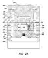
- FIG. 2Ais a cross section view showing the relative position of the Ge layer with respect to the layers of the silicon circuit.
- FIG. 2Bis another cross section view showing the relative position of the Ge layer.
- FIG. 3shows an individually addressable pixel array wherein selection of a particular row address circuit and a particular column readout circuit uniquely identifies the light intensity at a given pixel.
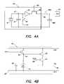
- FIGS. 4A and 4Billustrate exemplary circuits within a pixel used to collect and amplify the charge received in each photodetector.
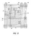
- FIG. 5shows the layout of a pixel that integrates the silicon circuit of FIG. 2 with a germanium photodetector.
- FIG. 6is a three dimensional depiction of the pixel layout levels.
- FIG. 7illustrates an exemplary circuit in a pixel used to collect time-of-flight and intensity information.
- FIG. 1is a schematic flow diagram of a preferred method of fabricating an image sensor. The method will also be described by reference to FIGS. 2A and 2B .
- FIG. 2Adisplays the final device structure through metallization and the inclusion of a microlens on each pixel
- FIG. 2Bdisplays the cross section of the device including a Ge seed layer.
- the first step in the fabrication processis to provide a substrate comprising silicon.
- the siliconis selected or chosen to have the resistivity and crystal orientation appropriate for the chosen silicon device processing technology, usually CMOS or BiCMOS processing.
- the next step (Block B)is to fabricate components of the silicon readout integrated circuitry (ROIC) in the silicon substrate in accordance with the chosen silicon processing technique.
- ROICsilicon readout integrated circuitry
- an exemplary fabricationbegins with a silicon substrate 200 .
- a shallow trench isolation 202is formed, followed by a transistor well 204 .
- a gate stack 206consisting of a thin insulating layer and a layer of conducting gate material is deposited or grown and patterned. Spacers 208 are then deposited and etched using anisotropic etching. After spacer formation, source and drain regions 210 are formed through implantation or other means such as selective epitaxy and annealed if necessary. The source/drain annealing is usually the final high temperature process (900-1050° C. for 1-30 s). Once the sources and drains are completed, the thermal budget must be limited to avoid solid state diffusion.
- the first dielectric 212is then formed in a conventional manner using a low temperature (350-750° C.) deposition process and planarized as by chemical mechanical polishing (CMP).
- the dielectric 212can be silicon oxide, silicon oxynitride, or any similarly low dielectric constant material.
- the third step(Block C of FIG. 1 ) is to form an array of epitaxially grown photodetectors comprising germanium overlying the silicon.
- the germanium photodetectorsare formed from an array of small isolated germanium islands epitaxially grown within openings on a dielectric clad surface of the substrate. The growth and dimensions of the islands are chosen to provide low defect growth. As a result, the germanium photodetectors are monolithically integrated with the silicon circuitry.
- a standard core silicon processis interrupted to include growth of a Ge absorption layer.
- a thin silicon nitride layer 214that will act as an etch stop later in the process is deposited.
- a dielectric 216(this dielectric could be the same or different material to that used for 212 ) is deposited on the surface 214 to a thickness corresponding to the required thickness of the Ge absorption layer. The optimum thickness will depend on the wavelength of light to be detected. For example, at a wavelength of 1.3 ⁇ m, the lowest noise equivalent power is obtained at approximately 1.3 ⁇ m.
- the optimum Ge thicknessis about 2.3 ⁇ m.
- the Ge thicknessshould be sufficient to absorb at least 1% of the incident light in the wavelength range 400 to 1700 nm.
- the well region 218is formed by patterning the surface with resist and etching dielectric 216 using a plasma etch that is selective to dielectric 216 over nitride 214 [5].
- the remainder of nitride 214can be etched away using a solution of hot phosphoric acid or by a carefully timed plasma etch.
- oxide 220is formed through conformal deposition.
- the seed window 217is formed by patterning the exposed portion of dielectric 212 and etching to the silicon substrate.
- Undoped Ge selective epitaxial growth (SEG)is then performed to fill the seed channel 217 and the Ge well 218 .
- the background doping during epitaxyshould be restricted as much as possible by taking precautions well known in the art of epitaxy.
- Chemical-mechanical polishing (CMP)is then used to planarize the resulting Ge growth to form a Ge region 218 that is flush with the surrounding dielectric 216 .
- a thin selective silicon layer 222is then grown on the surface of 218 and partially oxidized.
- a p-i-n photodetectorcan then be made by implanting p-type dopant (e.g. boron) to form contact region 224 and by implanting n-type dopant (e.g. phosphorous) to form contact region 226 .
- p-type dopante.g. boron
- n-type dopante.g. phosphorous
- Dielectric 228is then deposited on the structure.
- the absorption layer described aboveis germanium, it should be realized that one could equally well use an alloy of silicon and germanium, (Si 1-x Ge x ) where x is varied from 0 to 100 percent. In that case, there would be a trade-off between the cutoff wavelength and the dark current. As the Ge fraction x is decreased, the dark current becomes lower and the cutoff wavelength becomes smaller.
- the next step, shown as Block D of FIG. 1is to form contacts and metallization to interconnect the Ge photodetectors with the silicon ROIC circuit.
- vias 230 that contact the source/drains (or emitter, base, and collector of bipolar devices) of the transistors and the anode and cathode of the photodetectorare etched from the surface through all the dielectric materials.
- the stack of dielectric materialsincludes dielectric 214 that may behave differently in the etching plasma.
- the remainder of the process, which includes backend metallization steps,proceeds as usual with two notable exceptions to be detailed later.
- the viasare etched, they are filled with a conducting metal such as tungsten and then polished in the usual manner. Succeeding dielectric and metal layers are formed using standard processes.
- the usual backend processcan be modified to include a filter for a specific wavelength or band of wavelengths.
- a filter material 236 capable of filtering specific wavelengthscan be deposited and patterned above the photodetector after planarizing one of the interlevel dielectric layers.
- the backend metal lines themselvescan be patterned appropriately to be used as a filter for visible and infrared radiation incident on each of the pixel sensors [6].
- a microlens 244can be deposited, patterned, and flowed above each pixel to improve the effective fill factor of each pixel element.
- the layercan be formed by other methods such as solid phase epitaxy, hydrogen implantation and wafer bonding, liquid phase epitaxy, and other techniques known in the art.
- FIG. 3is a block diagram of the exemplary imager.
- the imager 30comprises a row address circuit 31 , an array of pixels 32 , each containing a germanium photodetection layer, a column readout circuit 33 , an analog-to-digital converter (ADC) 34 and output buffer 35 which the drives the chip output 36 . There are also clocks and control logic, not shown in the figure.
- the row addressing circuit 31selects one of a plurality of row address lines 37 . Each row address line is connected to a plurality of pixels 32 , one for each of the columns of the array. All the pixels in a given row are selected simultaneously by the row address line.
- Each pixel 32 in the selected rowcharges its column bus 38 to a voltage related to the accumulated illumination which that pixel has received since the last time it was reset. Only one row at a time is selected, so that the other pixels in the same column connected to the same column bus do not influence the voltage on the column bus.
- the combination of row address and selected columnuniquely identify each pixel. By successively addressing each row in turn, and successively sampling and holding each column bus while each row is selected, the light intensity at each pixel of the array is detected, and an image may be formed.
- the analog voltage from the column buffersis converted to digital form by the analog-to-digital converter 34 and sent to the output buffer 35 before leaving the chip on the output bus 36 .
- other patterns of pixelsmight also be used, such as a hexagonal grid of pixels, a checkerboard pattern of pixels, or, for some applications, even a single line of pixels, without departing from the scope of the invention.
- an exemplary pixel 40is comprised of a germanium photodiode 41 , an integration capacitor 42 , an amplifier 43 , a row selection transistor 44 which determines when the pixel is connected to the column bus 38 , and a reset circuit 45 .
- the integration capacitor 42need not be a separate element, but may be constituted by the intrinsic capacitance of the photodetector and the amplifier input capacitance in parallel with other stray capacitances.
- Sample-and-hold circuits 46 A or 46 B in the column readout block ( 33 of FIG. 3 )successively read each column of the array, and their outputs are digitized by the ADC 44 .
- the pixel integration capacitor 42is charged to a reference voltage by the reset switch 45 . As light falls on the photodetector, current is generated, which discharges the capacitor 42 . The floating node 47 of the capacitor is input to the amplifier 48 .
- the ROW select signal 22is asserted, and the row transistor 44 puts the amplified output of the pixel on the COL bus 38 , where it is read by the sample-and-hold circuit 46 A, 46 B in the column readout block. The pixel 40 is then reset and the next integration period begins.
- FIG. 4Bis a more specific example of a FIG. 4A circuit.
- the reset circuit 45is a single transistor and the amplifier 43 is a single-transistor source-follower circuit.
- the total pixel circuitry in this caseis only three transistors.
- FIG. 5shows that such a pixel can be laid out in a compact fashion
- FIG. 6shows a three dimensional perspective view of the same pixel.
- the germanium layer 50is the large element in the pixel, giving a high fill factor (i.e. a large percentage of the cell is responsive to illumination.)
- the reset transistor 51 , the source follower transistor 52 and the row selection transistor 53are formed in the silicon substrate underneath the germanium pixel.
- the power line 54 and the ground line 55run parallel to the row select lines 22 on one level of metal, and the reset line 56 and column 38 line run perpendicular on a second metal level.
- the floating node 58which constitutes one plate of the integration capacitor ( 42 of FIG.
- FIG. 7shows an alternative embodiment of a pixel array imager which is optimized for time-of-flight imaging.
- each pixel 701measures not simply the total amount of illumination falling on the pixel, but the peaks of the illumination intensity and the times at which those peaks occur.
- the FIG. 7 imagercan be used in a distance measuring camera, where the distance to remote objects is measured by illuminating the scene with a flash of infrared light, and the time at which reflections return to the camera directly measures the distance to each part of the scene.
- the architecture of pixel 701 for this applicationis relatively sophisticated.
- the output of the photodiode 702is fed into a fast low-noise amplifier 703 .
- the amplified signalhas DC and low-frequency components removed by the filter 704 before being further amplified by the amplifier 705 and entering the peak detector 706 .
- the peak detectorproduces an output each time the incoming signal rises to a peak and then falls again, corresponding to reflections from objects more distant in the field of view of the pixel.
- the intensity of the peak 707is recorded on a storage capacitor 708 , and the presence of the peak is used to switch an on-chip voltage ramp 709 between a plurality of storage capacitors 710 .
- the voltage ramp 709begins to rise when the flash is sent out.
- the value of the rampis frozen on that capacitor and serves as a measure of the time at which the reflection arrived.
- the multiplexors 711 and 712the arrival times and the peak intensities of a number of reflections from one part of the scene are recorded. After all reflections have returned, the voltages on the timing capacitors 710 and the intensity capacitors 708 are read out through the output multiplexor 713 and pixel output amplifier 714 .
- a constant current sourcecan be applied to the timing capacitors.
- the total charge collected on the time capacitorswould be a measure of the time-of-flight.
- a single intensity capacitor and single timing capacitorcan be used at each pixel if only a single pulse return is desired.
- the threshold used for peak detectioncan be varied adaptively with time.
- a digital timing signalcan be frozen on digital storage elements in each pixel.
- An array of germanium photosensitive elementsis thus integrated with silicon readout circuits to form an infrared imager.
- the silicon transistorsare formed first, using silicon wafer fabrication techniques well known to those skilled in the art.
- the germanium elementsare added in a subsequent step, and wafer fabrication techniques are applied to form germanium photodiodes.
- the temperatures needed for germanium processingare lower than those necessary for silicon processing, thus the germanium devices can be formed without affecting the previously formed silicon devices.
- Insulating and metallic layersare then deposited and patterned to form the circuit wiring and to connect the germanium devices to the silicon circuits.
- the substrateincludes integrated silicon circuitry connected to the photodetectors to individually address and read the photoresponses of the photodetectors.
- the substratehas an outer dielectric clad surface that includes openings.
- the isolated islands comprising germaniumare disposed in the openings and integrated with the silicon by epitaxial growth.
- the outer surfaceis planar, and the islands have outer surfaces co-planar with the silicon.
- the islandsshould have sufficient thickness to absorb the least 1% of the incident light in the wavelength range 400 to 1700 nanometers.
- the substrate and the islandsare advantageously monocrystalline material and can be crystallographically aligned.
- One or more of the islandscan include a plurality of p-n junctions at different respective depths in order to distinguish the spectrum of light absorbed by the island.
- the islandsare formed by the process described in U.S. patent application Ser. No. 10/510,932.
- Components of the integrated circuitry formed within the substratecan be connected together and connected to the photodetectors by a common metallization layer.
- the integrated circuitrycan, for time-of-flight imaging, be configured to measure peaks in the incident light.
- the advantages of the inventionare manyfold.
- the advantagesinclude the following:
Landscapes
- Engineering & Computer Science (AREA)
- Physics & Mathematics (AREA)
- Condensed Matter Physics & Semiconductors (AREA)
- General Physics & Mathematics (AREA)
- Manufacturing & Machinery (AREA)
- Computer Hardware Design (AREA)
- Microelectronics & Electronic Packaging (AREA)
- Power Engineering (AREA)
- Chemical & Material Sciences (AREA)
- Materials Engineering (AREA)
- Solid State Image Pick-Up Elements (AREA)
- Transforming Light Signals Into Electric Signals (AREA)
Abstract
Description
- A short wave infrared detector array on a silicon substrate with sensitivity to 1.7 μm
- The ability to form such an array with low dark current
- The ability to form such an array with high frequency response
- High quantum efficiency array by controlling well depth of individual detectors
- Germanium absorption layer lies above the substrate allowing transistors to occupy the underlying area thereby increasing the fill factor
- High uniformity across the array due to the use of well established Si processing techniques
- Low pixel cross talk since carrier diffusion between pixels is impossible
- High density and high speed transistors as well as other components can be integrated with the array
- Complete reuse of process models and standard cells due to modular integration
- Pixel size can be made extremely small thus reducing the resulting imager size for a given number of pixels, allowing smaller and lighter weight camera optics to be used
- Pixel size can be made extremely small thus allowing high resolution arrays for a given imager area
- Same metallization process used to contact Ge devices, Si devices, and passive components
- This technology takes advantage of silicon scaling rates by allowing an improvement in fill factor or an increase in electronic complexity as linewidths shrink. The pitch in hybridized arrays is substantially unchanged in the last decade.
- Indium bump bond hybridization is not required thereby increasing reliability and yield
- Hybridization is not required therefore reducing cost
- Low capacitance connections from IR photodiode to circuit
Claims (18)
Priority Applications (5)
| Application Number | Priority Date | Filing Date | Title |
|---|---|---|---|
| US10/964,057US7453129B2 (en) | 2002-12-18 | 2004-10-13 | Image sensor comprising isolated germanium photodetectors integrated with a silicon substrate and silicon circuitry |
| US12/271,601US7973377B2 (en) | 2002-12-18 | 2008-11-14 | Image sensor comprising isolated germanium photodetectors integrated with a silicon substrate and silicon circuitry |
| US13/116,411US8664739B2 (en) | 2002-12-18 | 2011-05-26 | Image sensor comprising isolated germanium photodetectors integrated with a silicon substrate and silicon circuitry |
| US14/195,590US9142585B2 (en) | 2002-12-18 | 2014-03-03 | Image sensor comprising isolated germanium photodetectors integrated with a silicon substrate and silicon circuitry |
| US14/835,539US20150364515A1 (en) | 2002-12-18 | 2015-08-25 | Image sensor comprising isolated germanium photodetectors integrated with a silicon substrate and silicon circuitry |
Applications Claiming Priority (4)
| Application Number | Priority Date | Filing Date | Title |
|---|---|---|---|
| US43435902P | 2002-12-18 | 2002-12-18 | |
| US10/453,037US7012314B2 (en) | 2002-12-18 | 2003-06-03 | Semiconductor devices with reduced active region defects and unique contacting schemes |
| US51093203P | 2003-10-13 | 2003-10-13 | |
| US10/964,057US7453129B2 (en) | 2002-12-18 | 2004-10-13 | Image sensor comprising isolated germanium photodetectors integrated with a silicon substrate and silicon circuitry |
Related Parent Applications (1)
| Application Number | Title | Priority Date | Filing Date |
|---|---|---|---|
| US10/453,037Continuation-In-PartUS7012314B2 (en) | 2002-12-18 | 2003-06-03 | Semiconductor devices with reduced active region defects and unique contacting schemes |
Related Child Applications (1)
| Application Number | Title | Priority Date | Filing Date |
|---|---|---|---|
| US12/271,601ContinuationUS7973377B2 (en) | 2002-12-18 | 2008-11-14 | Image sensor comprising isolated germanium photodetectors integrated with a silicon substrate and silicon circuitry |
Publications (2)
| Publication Number | Publication Date |
|---|---|
| US20050205954A1 US20050205954A1 (en) | 2005-09-22 |
| US7453129B2true US7453129B2 (en) | 2008-11-18 |
Family
ID=46303076
Family Applications (5)
| Application Number | Title | Priority Date | Filing Date |
|---|---|---|---|
| US10/964,057Expired - LifetimeUS7453129B2 (en) | 2002-12-18 | 2004-10-13 | Image sensor comprising isolated germanium photodetectors integrated with a silicon substrate and silicon circuitry |
| US12/271,601Expired - Fee RelatedUS7973377B2 (en) | 2002-12-18 | 2008-11-14 | Image sensor comprising isolated germanium photodetectors integrated with a silicon substrate and silicon circuitry |
| US13/116,411Expired - Fee RelatedUS8664739B2 (en) | 2002-12-18 | 2011-05-26 | Image sensor comprising isolated germanium photodetectors integrated with a silicon substrate and silicon circuitry |
| US14/195,590Expired - LifetimeUS9142585B2 (en) | 2002-12-18 | 2014-03-03 | Image sensor comprising isolated germanium photodetectors integrated with a silicon substrate and silicon circuitry |
| US14/835,539AbandonedUS20150364515A1 (en) | 2002-12-18 | 2015-08-25 | Image sensor comprising isolated germanium photodetectors integrated with a silicon substrate and silicon circuitry |
Family Applications After (4)
| Application Number | Title | Priority Date | Filing Date |
|---|---|---|---|
| US12/271,601Expired - Fee RelatedUS7973377B2 (en) | 2002-12-18 | 2008-11-14 | Image sensor comprising isolated germanium photodetectors integrated with a silicon substrate and silicon circuitry |
| US13/116,411Expired - Fee RelatedUS8664739B2 (en) | 2002-12-18 | 2011-05-26 | Image sensor comprising isolated germanium photodetectors integrated with a silicon substrate and silicon circuitry |
| US14/195,590Expired - LifetimeUS9142585B2 (en) | 2002-12-18 | 2014-03-03 | Image sensor comprising isolated germanium photodetectors integrated with a silicon substrate and silicon circuitry |
| US14/835,539AbandonedUS20150364515A1 (en) | 2002-12-18 | 2015-08-25 | Image sensor comprising isolated germanium photodetectors integrated with a silicon substrate and silicon circuitry |
Country Status (1)
| Country | Link |
|---|---|
| US (5) | US7453129B2 (en) |
Cited By (23)
| Publication number | Priority date | Publication date | Assignee | Title |
|---|---|---|---|---|
| US20080121805A1 (en)* | 2006-11-04 | 2008-05-29 | Tweet Douglas J | Ge short wavelength infrared imager |
| US20100019154A1 (en)* | 2008-07-28 | 2010-01-28 | Noble Peak Vision Corp. | Imaging apparatus and methods |
| US20100059802A1 (en)* | 2008-09-11 | 2010-03-11 | Shenlin Chen | Image sensor with raised photosensitive elements |
| US20100078750A1 (en)* | 2008-10-01 | 2010-04-01 | Oh-Jin Jung | Image sensor and method for fabricating the same |
| US20110049365A1 (en)* | 2009-08-31 | 2011-03-03 | Aebi Verle W | Low energy portable low-light camera with wavelength cutoff |
| US8084739B2 (en) | 2008-07-16 | 2011-12-27 | Infrared Newco., Inc. | Imaging apparatus and methods |
| US20120043637A1 (en)* | 2002-12-18 | 2012-02-23 | Infrared Newco, Inc. | Image sensor comprising isolated germanium photodetectors integrated with a silicon substrate and silicon circuitry |
| US8139130B2 (en) | 2005-07-28 | 2012-03-20 | Omnivision Technologies, Inc. | Image sensor with improved light sensitivity |
| US8194296B2 (en) | 2006-05-22 | 2012-06-05 | Omnivision Technologies, Inc. | Image sensor with improved light sensitivity |
| US8274715B2 (en) | 2005-07-28 | 2012-09-25 | Omnivision Technologies, Inc. | Processing color and panchromatic pixels |
| US8416339B2 (en) | 2006-10-04 | 2013-04-09 | Omni Vision Technologies, Inc. | Providing multiple video signals from single sensor |
| US8546250B2 (en) | 2011-08-18 | 2013-10-01 | Wafertech Llc | Method of fabricating vertical integrated semiconductor device with multiple continuous single crystal silicon layers vertically separated from one another |
| US8790954B2 (en) | 2006-05-09 | 2014-07-29 | Taiwan Semiconductor Manufacturing Company, Ltd. | Method of making wafer structure for backside illuminated color image sensor |
| US9748429B1 (en) | 2013-06-11 | 2017-08-29 | National Technology & Engineering Solutions Of Sandia, Llc | Avalanche diode having reduced dark current and method for its manufacture |
| US9864138B2 (en) | 2015-01-05 | 2018-01-09 | The Research Foundation For The State University Of New York | Integrated photonics including germanium |
| US10698156B2 (en) | 2017-04-27 | 2020-06-30 | The Research Foundation For The State University Of New York | Wafer scale bonded active photonics interposer |
| US10816724B2 (en) | 2018-04-05 | 2020-10-27 | The Research Foundation For The State University Of New York | Fabricating photonics structure light signal transmission regions |
| US10877300B2 (en) | 2018-04-04 | 2020-12-29 | The Research Foundation For The State University Of New York | Heterogeneous structure on an integrated photonics platform |
| US10976491B2 (en) | 2016-11-23 | 2021-04-13 | The Research Foundation For The State University Of New York | Photonics interposer optoelectronics |
| US10998386B2 (en)* | 2017-11-09 | 2021-05-04 | Lockheed Martin Corporation | Display-integrated infrared emitter and sensor structures |
| EP4167269A1 (en)* | 2021-10-15 | 2023-04-19 | Infineon Technologies AG | Heteroepitaxial semiconductor device and method for fabricating a heteroepitaxial semiconductor device |
| US12027555B2 (en) | 2021-05-10 | 2024-07-02 | United Microelectronics Corp. | Image sensor |
| US12317757B2 (en) | 2018-10-11 | 2025-05-27 | SeeQC, Inc. | System and method for superconducting multi-chip module |
Families Citing this family (84)
| Publication number | Priority date | Publication date | Assignee | Title |
|---|---|---|---|---|
| US7057256B2 (en) | 2001-05-25 | 2006-06-06 | President & Fellows Of Harvard College | Silicon-based visible and near-infrared optoelectric devices |
| US7442629B2 (en) | 2004-09-24 | 2008-10-28 | President & Fellows Of Harvard College | Femtosecond laser-induced formation of submicrometer spikes on a semiconductor substrate |
| WO2005094254A2 (en)* | 2004-03-17 | 2005-10-13 | The Board Of Trustees Of The Leland Stanford Junior University | Crystalline-type device and approach therefor |
| US7749872B2 (en)* | 2004-03-17 | 2010-07-06 | The Board Of Trustees Of The Leland Stanford Junior University | Crystalline-type device and approach therefor |
| US7008813B1 (en)* | 2005-02-28 | 2006-03-07 | Sharp Laboratories Of America, Inc.. | Epitaxial growth of germanium photodetector for CMOS imagers |
| US8324660B2 (en) | 2005-05-17 | 2012-12-04 | Taiwan Semiconductor Manufacturing Company, Ltd. | Lattice-mismatched semiconductor structures with reduced dislocation defect densities and related methods for device fabrication |
| US9153645B2 (en) | 2005-05-17 | 2015-10-06 | Taiwan Semiconductor Manufacturing Company, Ltd. | Lattice-mismatched semiconductor structures with reduced dislocation defect densities and related methods for device fabrication |
| US20070001100A1 (en)* | 2005-06-30 | 2007-01-04 | Taiwan Semiconductor Manufacturing Company, Ltd. | Light reflection for backside illuminated sensor |
| US7358107B2 (en)* | 2005-10-27 | 2008-04-15 | Sharp Laboratories Of America, Inc. | Method of fabricating a germanium photo detector on a high quality germanium epitaxial overgrowth layer |
| KR101316947B1 (en)* | 2005-11-01 | 2013-10-15 | 메사추세츠 인스티튜트 오브 테크놀로지 | Monolithically integrated semiconductor materials and devices |
| WO2007067589A2 (en)* | 2005-12-05 | 2007-06-14 | Massachusetts Institute Of Technology | Insulated gate devices and method of making same |
| US7629661B2 (en)* | 2006-02-10 | 2009-12-08 | Noble Peak Vision Corp. | Semiconductor devices with photoresponsive components and metal silicide light blocking structures |
| WO2007112066A2 (en) | 2006-03-24 | 2007-10-04 | Amberwave Systems Corporation | Lattice-mismatched semiconductor structures and related methods for device fabrication |
| US8704277B2 (en)* | 2006-05-09 | 2014-04-22 | Taiwan Semiconductor Manufacturing Company, Ltd. | Spectrally efficient photodiode for backside illuminated sensor |
| US8063397B2 (en)* | 2006-06-28 | 2011-11-22 | Massachusetts Institute Of Technology | Semiconductor light-emitting structure and graded-composition substrate providing yellow-green light emission |
| US7791170B2 (en) | 2006-07-10 | 2010-09-07 | Taiwan Semiconductor Manufacturing Company, Ltd. | Method of making a deep junction for electrical crosstalk reduction of an image sensor |
| US8173551B2 (en) | 2006-09-07 | 2012-05-08 | Taiwan Semiconductor Manufacturing Co., Ltd. | Defect reduction using aspect ratio trapping |
| WO2008039534A2 (en) | 2006-09-27 | 2008-04-03 | Amberwave Systems Corporation | Quantum tunneling devices and circuits with lattice- mismatched semiconductor structures |
| US8502263B2 (en) | 2006-10-19 | 2013-08-06 | Taiwan Semiconductor Manufacturing Company, Ltd. | Light-emitter-based devices with lattice-mismatched semiconductor structures |
| US20080217717A1 (en)* | 2007-03-09 | 2008-09-11 | Lockheed Martin Corporation | Cte matched multiplexor |
| EP2088624A3 (en)* | 2007-04-05 | 2009-11-18 | Fraunhofer-Gesellschaft zur Förderung der Angewandten Forschung e.V. | Integrated optical construction element with photonic crystal |
| US7825328B2 (en) | 2007-04-09 | 2010-11-02 | Taiwan Semiconductor Manufacturing Company, Ltd. | Nitride-based multi-junction solar cell modules and methods for making the same |
| US8237151B2 (en) | 2009-01-09 | 2012-08-07 | Taiwan Semiconductor Manufacturing Company, Ltd. | Diode-based devices and methods for making the same |
| US8304805B2 (en) | 2009-01-09 | 2012-11-06 | Taiwan Semiconductor Manufacturing Company, Ltd. | Semiconductor diodes fabricated by aspect ratio trapping with coalesced films |
| WO2008124154A2 (en) | 2007-04-09 | 2008-10-16 | Amberwave Systems Corporation | Photovoltaics on silicon |
| US8329541B2 (en) | 2007-06-15 | 2012-12-11 | Taiwan Semiconductor Manufacturing Company, Ltd. | InP-based transistor fabrication |
| JP2010538495A (en) | 2007-09-07 | 2010-12-09 | アンバーウェーブ・システムズ・コーポレーション | Multi-junction solar cell |
| US7999342B2 (en) | 2007-09-24 | 2011-08-16 | Taiwan Semiconductor Manufacturing Company, Ltd | Image sensor element for backside-illuminated sensor |
| US20090114964A1 (en)* | 2007-11-05 | 2009-05-07 | Chang-Hun Han | Image sensor and method for manufacturing the same |
| US20090219403A1 (en)* | 2008-02-29 | 2009-09-03 | Sionyx, Inc. | Compact passive low-light imaging apparatus |
| US7888758B2 (en)* | 2008-03-12 | 2011-02-15 | Aptina Imaging Corporation | Method of forming a permanent carrier and spacer wafer for wafer level optics and associated structure |
| US8183667B2 (en) | 2008-06-03 | 2012-05-22 | Taiwan Semiconductor Manufacturing Co., Ltd. | Epitaxial growth of crystalline material |
| EP2133918B1 (en)* | 2008-06-09 | 2015-01-28 | Sony Corporation | Solid-state imaging device, drive method thereof and electronic apparatus |
| US8274097B2 (en) | 2008-07-01 | 2012-09-25 | Taiwan Semiconductor Manufacturing Company, Ltd. | Reduction of edge effects from aspect ratio trapping |
| US8981427B2 (en) | 2008-07-15 | 2015-03-17 | Taiwan Semiconductor Manufacturing Company, Ltd. | Polishing of small composite semiconductor materials |
| EP2335273A4 (en)* | 2008-09-19 | 2012-01-25 | Taiwan Semiconductor Mfg | FORMATION OF DEVICES BY GROWTH OF EPITAXIAL LAYERS |
| US20100072515A1 (en) | 2008-09-19 | 2010-03-25 | Amberwave Systems Corporation | Fabrication and structures of crystalline material |
| US8253211B2 (en) | 2008-09-24 | 2012-08-28 | Taiwan Semiconductor Manufacturing Company, Ltd. | Semiconductor sensor structures with reduced dislocation defect densities |
| US8629446B2 (en) | 2009-04-02 | 2014-01-14 | Taiwan Semiconductor Manufacturing Company, Ltd. | Devices formed from a non-polar plane of a crystalline material and method of making the same |
| US9911781B2 (en) | 2009-09-17 | 2018-03-06 | Sionyx, Llc | Photosensitive imaging devices and associated methods |
| US9673243B2 (en) | 2009-09-17 | 2017-06-06 | Sionyx, Llc | Photosensitive imaging devices and associated methods |
| US8692198B2 (en) | 2010-04-21 | 2014-04-08 | Sionyx, Inc. | Photosensitive imaging devices and associated methods |
| US20110278687A1 (en)* | 2010-05-17 | 2011-11-17 | Fang-Ming Huang | Backside-illuminated sensor with noise reduction |
| WO2011160130A2 (en) | 2010-06-18 | 2011-12-22 | Sionyx, Inc | High speed photosensitive devices and associated methods |
| FR2964795B1 (en)* | 2010-09-09 | 2013-09-27 | Commissariat Energie Atomique | PHOTODETECTEUR AND CORRESPONDING DETECTION MATRIX |
| US20120065926A1 (en)* | 2010-09-14 | 2012-03-15 | Samsung Electronics Co., Ltd | Integrated motion sensing apparatus |
| US8912616B2 (en) | 2011-02-11 | 2014-12-16 | International Business Machines Corporaion | Device for detecting electromagnetic radiation comprising a diffusion junction and a resonant grating in a single layer |
| US9496308B2 (en) | 2011-06-09 | 2016-11-15 | Sionyx, Llc | Process module for increasing the response of backside illuminated photosensitive imagers and associated methods |
| WO2013010127A2 (en) | 2011-07-13 | 2013-01-17 | Sionyx, Inc. | Biometric imaging devices and associated methods |
| US9064764B2 (en) | 2012-03-22 | 2015-06-23 | Sionyx, Inc. | Pixel isolation elements, devices, and associated methods |
| WO2013155145A1 (en) | 2012-04-10 | 2013-10-17 | Drs Rsta, Inc. | High density capacitor integrated into focal plane array processing flow |
| US8796747B2 (en) | 2013-01-08 | 2014-08-05 | International Business Machines Corporation | Photonics device and CMOS device having a common gate |
| US8802484B1 (en)* | 2013-01-22 | 2014-08-12 | Globalfoundries Singapore Pte. Ltd. | Integration of germanium photo detector in CMOS processing |
| US9762830B2 (en) | 2013-02-15 | 2017-09-12 | Sionyx, Llc | High dynamic range CMOS image sensor having anti-blooming properties and associated methods |
| WO2014151093A1 (en) | 2013-03-15 | 2014-09-25 | Sionyx, Inc. | Three dimensional imaging utilizing stacked imager devices and associated methods |
| US9659992B2 (en) | 2013-03-21 | 2017-05-23 | Infineon Technologies Ag | Method of manufacturing an imager and imager device |
| US9209345B2 (en) | 2013-06-29 | 2015-12-08 | Sionyx, Inc. | Shallow trench textured regions and associated methods |
| US10050015B2 (en)* | 2014-03-27 | 2018-08-14 | Intel Corporation | Multi-device flexible electronics system on a chip (SOC) process integration |
| CN107112335B (en)* | 2014-11-24 | 2019-05-31 | 光澄科技股份有限公司 | Monolithic integration technique for manufacturing photodetectors and transistors on the same substrate |
| US9478689B2 (en)* | 2014-12-10 | 2016-10-25 | Sifotonics Technologies Co., Ltd. | High-speed germanium on silicon avalanche photodiode |
| US20160225812A1 (en) | 2015-02-03 | 2016-08-04 | Microsoft Technology Licensing, Llc | Cmos depth image sensor with integrated shallow trench isolation structures |
| US10435814B2 (en) | 2015-10-30 | 2019-10-08 | The Board Of Trustees Of The Leland Stanford Junior University | Single metal crystals |
| US10867834B2 (en)* | 2015-12-31 | 2020-12-15 | Taiwan Semiconductor Manufacturing Company Ltd. | Semiconductor structure and manufacturing method thereof |
| US10128302B2 (en)* | 2016-01-28 | 2018-11-13 | Ams Sensors Uk Limited | IR detector array device |
| WO2017151055A1 (en)* | 2016-02-29 | 2017-09-08 | Nanyang Technological University | Optical structure and method of forming the same |
| US9711662B1 (en)* | 2016-04-21 | 2017-07-18 | Globalfoundries Singapore Pte. Ltd. | Integrated circuits with optical modulators and photodetectors and methods for producing the same |
| KR102259759B1 (en)* | 2016-05-13 | 2021-06-02 | 한국전자기술연구원 | Readout integrated circuit structure capable of inputting and outputing simultaneously and lidar tof sensor including the same |
| JP7007088B2 (en)* | 2016-12-07 | 2022-01-24 | ソニーセミコンダクタソリューションズ株式会社 | Light receiving elements, image sensors and electronic devices |
| US10892295B2 (en)* | 2018-01-10 | 2021-01-12 | Microsoft Technology Licensing, Llc | Germanium-modified, back-side illuminated optical sensor |
| US11888014B2 (en) | 2018-01-12 | 2024-01-30 | Zedel Sàrl | Short-wave infrared detector and its integration with CMOS compatible substrates |
| US10690853B2 (en) | 2018-06-25 | 2020-06-23 | International Business Machines Corporation | Optoelectronics integration using semiconductor on insulator substrate |
| TWI829761B (en) | 2018-11-21 | 2024-01-21 | 紐約州立大學研究基金會 | Photonics structure with integrated laser |
| US11550099B2 (en) | 2018-11-21 | 2023-01-10 | The Research Foundation For The State University Of New York | Photonics optoelectrical system |
| TWI851601B (en) | 2018-11-21 | 2024-08-11 | 紐約州立大學研究基金會 | Photonics optoelectrical system and method for fabricating same |
| US11004878B2 (en) | 2019-08-19 | 2021-05-11 | Globalfoundries U.S. Inc. | Photodiodes integrated into a BiCMOS process |
| US11196947B2 (en)* | 2019-09-17 | 2021-12-07 | New Imaging Technologies | Optical sensor |
| US11282883B2 (en) | 2019-12-13 | 2022-03-22 | Globalfoundries U.S. Inc. | Trench-based photodiodes |
| US12094891B2 (en) | 2020-07-13 | 2024-09-17 | Drs Network & Imaging Systems, Llc | High-density capacitor for focal plane arrays |
| US12015099B2 (en)* | 2020-08-01 | 2024-06-18 | Taiwan Semiconductor Manufacturing Co., Ltd. | Semiconductor sensor and methods thereof |
| US11367745B2 (en)* | 2020-08-20 | 2022-06-21 | Taiwan Semiconductor Manufacturing Co., Ltd. | Apparatus and methods for sensing long wavelength light |
| US20230369518A1 (en) | 2021-05-04 | 2023-11-16 | Artilux, Inc. | Optical sensing apparatus |
| US12364036B2 (en) | 2021-08-28 | 2025-07-15 | Taiwan Semiconductor Manufacturing Company Limited | Germanium-based photodetector with reduced dark current |
| CN114597226B (en)* | 2022-05-10 | 2022-07-29 | 浙江兴芯半导体有限公司 | A kind of manufacturing method of image sensor based on germanium p-i-n photodiode |
| CN116666500B (en)* | 2023-07-24 | 2023-11-03 | 上海铭锟半导体有限公司 | Germanium photodetectors and methods to improve their long-wavelength response through thermal mismatch stress |
Citations (65)
| Publication number | Priority date | Publication date | Assignee | Title |
|---|---|---|---|---|
| US3971065A (en) | 1975-03-05 | 1976-07-20 | Eastman Kodak Company | Color imaging array |
| US4011016A (en) | 1974-04-30 | 1977-03-08 | Martin Marietta Corporation | Semiconductor radiation wavelength detector |
| US4038680A (en) | 1972-12-29 | 1977-07-26 | Sony Corporation | Semiconductor integrated circuit device |
| US4238760A (en) | 1978-10-06 | 1980-12-09 | Recognition Equipment Incorporated | Multi-spectrum photodiode devices |
| US4309604A (en) | 1978-07-24 | 1982-01-05 | Sharp Kabushiki Kaisha | Apparatus for sensing the wavelength and intensity of light |
| US4613895A (en) | 1977-03-24 | 1986-09-23 | Eastman Kodak Company | Color responsive imaging device employing wavelength dependent semiconductor optical absorption |
| US4651001A (en) | 1983-12-19 | 1987-03-17 | Kabushiki Kaisha Toshiba | Visible/infrared imaging device with stacked cell structure |
| US4677289A (en) | 1984-11-12 | 1987-06-30 | Kabushiki Kaisha Toshiba | Color sensor |
| US4952526A (en) | 1988-04-05 | 1990-08-28 | Thomson-Csf | Method for the fabrication of an alternation of layers of monocrystalline semiconducting material and layers of insulating material |
| US5120666A (en) | 1989-05-16 | 1992-06-09 | Fujitsu Limited | Manufacturing method for semiconductor device |
| US5158907A (en) | 1990-08-02 | 1992-10-27 | At&T Bell Laboratories | Method for making semiconductor devices with low dislocation defects |
| EP0538886A1 (en) | 1991-10-25 | 1993-04-28 | Canon Kabushiki Kaisha | Signal processor having avalanche photodiodes |
| US5221413A (en) | 1991-04-24 | 1993-06-22 | At&T Bell Laboratories | Method for making low defect density semiconductor heterostructure and devices made thereby |
| US5308980A (en) | 1991-02-20 | 1994-05-03 | Amber Engineering, Inc. | Thermal mismatch accommodated infrared detector hybrid array |
| US5326721A (en) | 1992-05-01 | 1994-07-05 | Texas Instruments Incorporated | Method of fabricating high-dielectric constant oxides on semiconductors using a GE buffer layer |
| US5371033A (en) | 1992-06-12 | 1994-12-06 | Gold Star Electron Co. | Method of making charge coupled device image sensor |
| US5442205A (en) | 1991-04-24 | 1995-08-15 | At&T Corp. | Semiconductor heterostructure devices with strained semiconductor layers |
| US5447117A (en)* | 1987-08-08 | 1995-09-05 | Canon Kabushiki Kaisha | Crystal article, method for producing the same and semiconductor device utilizing the same |
| US5467204A (en) | 1991-12-09 | 1995-11-14 | Sharp Kabushiki Kaisha | Liquid crystal light valve with dual function as both optical-to-electrical and optical-to-optical transducer |
| US5502299A (en) | 1994-12-12 | 1996-03-26 | Rockwell International Corporation | Current ratio circuit for multi-color imaging |
| US5668596A (en) | 1996-02-29 | 1997-09-16 | Eastman Kodak Company | Digital imaging device optimized for color performance |
| US5739562A (en) | 1995-08-01 | 1998-04-14 | Lucent Technologies Inc. | Combined photogate and photodiode active pixel image sensor |
| US5883421A (en) | 1997-03-13 | 1999-03-16 | University Pierre Et Marie Curie | Photodetector based on buried junctions and a corresponding method of manufacture |
| WO1999044224A1 (en) | 1998-02-27 | 1999-09-02 | North Carolina State University | Methods of fabricating gallium nitride semiconductor layers by lateral overgrowth through masks, and gallium nitride semiconductor structures fabricated thereby |
| US5965875A (en) | 1998-04-24 | 1999-10-12 | Foveon, Inc. | Color separation in an active pixel cell imaging array using a triple-well structure |
| EP0951055A2 (en) | 1998-04-17 | 1999-10-20 | Hewlett-Packard Company | Epitaxial material grown laterally within a trench |
| EP0967656A2 (en) | 1998-06-24 | 1999-12-29 | STMicroelectronics, Inc. | A solid state optical imaging pixel with a photosensitive resistive load |
| EP1005058A2 (en) | 1998-11-27 | 2000-05-31 | Kabushiki Kaisha Toshiba | Vacuum switchgear |
| JP2000340783A (en) | 1999-05-28 | 2000-12-08 | Sharp Corp | Method for manufacturing solid-state imaging device |
| US6287903B1 (en) | 1997-12-24 | 2001-09-11 | Texas Instruments Incorporated | Structure and method for a large-permittivity dielectric using a germanium layer |
| JP2001267544A (en) | 2000-03-21 | 2001-09-28 | Sharp Corp | Solid-state imaging device and method of manufacturing the same |
| US20010052597A1 (en) | 2000-06-20 | 2001-12-20 | U.S. Philips Corporation | Light-emitting matrix array display devices with light sensing elements |
| US20020011640A1 (en) | 2000-07-27 | 2002-01-31 | Andreas Bauer | Multispectral photodiode |
| US6352942B1 (en)* | 1999-06-25 | 2002-03-05 | Massachusetts Institute Of Technology | Oxidation of silicon on germanium |
| US20020039833A1 (en)* | 2000-08-04 | 2002-04-04 | Stmicroelectronics S.A. | Forming of quantum dots |
| US6396046B1 (en) | 1999-11-02 | 2002-05-28 | General Electric Company | Imager with reduced FET photoresponse and high integrity contact via |
| US20020072140A1 (en) | 2000-12-08 | 2002-06-13 | Motorola, Inc. | Quantum well infrared photodetector and method for fabricating same |
| US6410941B1 (en) | 2000-06-30 | 2002-06-25 | Motorola, Inc. | Reconfigurable systems using hybrid integrated circuits with optical ports |
| US6455360B1 (en) | 1995-06-26 | 2002-09-24 | Seiko Epson Corporation | Method for forming crystalline semiconductor layers, a method for fabricating thin film transistors, and a method for fabricating solar cells and active matrix liquid crystal devices |
| US20020135034A1 (en) | 1998-09-01 | 2002-09-26 | Keitaro Shigenaka | Multi-wavelength semiconductor image sensor and method of manufacturing the same |
| US6477285B1 (en) | 2000-06-30 | 2002-11-05 | Motorola, Inc. | Integrated circuits with optical signal propagation |
| US20020163023A1 (en) | 1999-12-01 | 2002-11-07 | Takashi Miida | Solid state imaging device, method of manufacturing the same, and solid state imaging system |
| WO2002090625A1 (en) | 2001-05-08 | 2002-11-14 | Btg International Limited | A method to produce germanium layers |
| US20020181825A1 (en) | 2001-06-01 | 2002-12-05 | Motorola, Inc. | Optical clock signal distribution |
| US20030010992A1 (en) | 2001-07-16 | 2003-01-16 | Motorola, Inc. | Semiconductor structure and method for implementing cross-point switch functionality |
| US20030010988A1 (en) | 2001-07-11 | 2003-01-16 | Motorola, Inc. | Structure and method for fabricating semiconductor structures with integrated optical components and controller |
| US20030013218A1 (en)* | 2001-07-10 | 2003-01-16 | Motorola, Inc. | Structure and method for fabricating semiconductor structures and devices for detecting chemical reactant |
| US20030016311A1 (en) | 2001-07-23 | 2003-01-23 | Nec Corporation | Liquid crystal display device |
| US20030015722A1 (en) | 2001-07-17 | 2003-01-23 | Motorola, Inc. | Structure and method for fabricating semiconductor structures and devices for dispersing a radiant energy transmission |
| US20030020078A1 (en) | 2001-07-25 | 2003-01-30 | Motorola, Inc. | Structure and method for fabricating semiconductor structures and devices with optical processing layers utilizing the formation of a compliant substrate for materials used to form the same |
| US20030103150A1 (en) | 2001-11-30 | 2003-06-05 | Catrysse Peter B. | Integrated color pixel ( ICP ) |
| US20030102469A1 (en)* | 2001-11-30 | 2003-06-05 | Jones Robert E. | Semiconductor device and method therefor |
| US20030148565A1 (en)* | 2001-02-01 | 2003-08-07 | Hideo Yamanaka | Method for forming thin semiconductor film, method for fabricating semiconductor device, system for executing these methods and electrooptic device |
| US20030148570A1 (en) | 1999-06-18 | 2003-08-07 | Rhodes Howard E. | CMOS imager with a self-aligned buried contact |
| US20030205710A1 (en) | 2002-05-06 | 2003-11-06 | Intel Corporation | Silicon and silicon/germanium light-emitting device, methods and systems |
| US6677655B2 (en) | 2000-08-04 | 2004-01-13 | Amberwave Systems Corporation | Silicon wafer with embedded optoelectronic material for monolithic OEIC |
| US20040012029A1 (en) | 1997-09-26 | 2004-01-22 | Bawolek Edward J | Method and apparatus for employing a light shield to modulate pixel color responsivity |
| US20040029325A1 (en) | 2000-06-23 | 2004-02-12 | Le Goascoz Vincent | Method for making a soi semiconductor substrate with thin active semiconductor layer |
| US20040079971A1 (en) | 2000-04-24 | 2004-04-29 | The University Of Connecticut | Imaging array utilizing thyristor-based pixel elements |
| WO2004061911A2 (en) | 2002-12-18 | 2004-07-22 | Agere Systems Inc. | Semiconductor devices with reduced active region defects and unique contacting schemes |
| US20040222463A1 (en) | 2003-05-09 | 2004-11-11 | Yee-Chia Yeo | SOI chip with mesa isolation and recess resistant regions |
| US6864557B2 (en) | 2001-06-18 | 2005-03-08 | Foveon, Inc. | Vertical color filter detector group and array |
| US6864111B2 (en) | 1998-02-02 | 2005-03-08 | E. I. Du Pont De Nemours And Company | Column-row addressable electric microswitch arrays and sensor matrices employing them |
| US6868138B2 (en) | 2002-05-29 | 2005-03-15 | The Regents Of The University Of Michigan | Method, processor and computed tomography (CT) machine for generating images utilizing high and low sensitivity data collected from a flat panel detector having an extended dynamic range |
| US6900499B2 (en) | 1997-08-29 | 2005-05-31 | Semiconductor Energy Laboratory Co., Ltd. | Non-volatile memory and semiconductor device |
Family Cites Families (73)
| Publication number | Priority date | Publication date | Assignee | Title |
|---|---|---|---|---|
| DE1264513C2 (en)* | 1963-11-29 | 1973-01-25 | Texas Instruments Inc | REFERENCE POTENTIAL FREE DC DIFFERENCE AMPLIFIER |
| JPS5832171A (en)* | 1981-07-27 | 1983-02-25 | Sumitomo Electric Ind Ltd | Optical voltage electric field sensor |
| JPS5955526A (en)* | 1982-09-24 | 1984-03-30 | Sharp Corp | interface circuit |
| JPS6191917A (en) | 1984-10-12 | 1986-05-10 | Nippon Telegr & Teleph Corp <Ntt> | Manufacture of semiconductor thin film crystal |
| JPH061219B2 (en) | 1985-03-25 | 1994-01-05 | 株式会社東芝 | Light receiving device |
| JPS6191917U (en) | 1984-11-24 | 1986-06-14 | ||
| US4725870A (en)* | 1985-11-18 | 1988-02-16 | American Telephone And Telegraph Company, At&T Bell Laboratories | Silicon germanium photodetector |
| JP2505754B2 (en)* | 1986-07-11 | 1996-06-12 | キヤノン株式会社 | Method for manufacturing photoelectric conversion device |
| US5281283A (en)* | 1987-03-26 | 1994-01-25 | Canon Kabushiki Kaisha | Group III-V compound crystal article using selective epitaxial growth |
| JP2929550B2 (en)* | 1989-06-07 | 1999-08-03 | キヤノン株式会社 | Optical sensor and image reading device |
| JPH0824193B2 (en)* | 1990-10-16 | 1996-03-06 | 工業技術院長 | Manufacturing method of semiconductor device for driving flat plate type light valve |
| CA2062134C (en)* | 1991-05-31 | 1997-03-25 | Ibm | Heteroepitaxial layers with low defect density and arbitrary network parameter |
| DE69313337T2 (en)* | 1992-04-17 | 1998-01-02 | Terumo Corp | Infrared sensor and method for its manufacture |
| JPH05335615A (en)* | 1992-05-27 | 1993-12-17 | Canon Inc | Photoelectric conversion device |
| JPH0767151B2 (en)* | 1993-02-25 | 1995-07-19 | 日本電気株式会社 | Infrared imaging device |
| EP0799495A4 (en)* | 1994-11-10 | 1999-11-03 | Lawrence Semiconductor Researc | SILICON-GERMANIUM-CARBON COMPOSITIONS AND RELATED PROCESSES |
| JP3243146B2 (en)* | 1994-12-08 | 2002-01-07 | 株式会社東芝 | Semiconductor device |
| JP3641511B2 (en)* | 1995-06-16 | 2005-04-20 | 株式会社ルネサステクノロジ | Semiconductor device |
| US5677538A (en)* | 1995-07-07 | 1997-10-14 | Trustees Of Boston University | Photodetectors using III-V nitrides |
| US5726440A (en)* | 1995-11-06 | 1998-03-10 | Spire Corporation | Wavelength selective photodetector |
| US5784187A (en)* | 1996-07-23 | 1998-07-21 | Lucent Technologies Inc. | Wafer level integration of an optical modulator and III-V photodetector |
| JP3063638B2 (en)* | 1996-09-20 | 2000-07-12 | 日本電気株式会社 | Semiconductor photodetector and method of manufacturing the same |
| US5770483A (en)* | 1996-10-08 | 1998-06-23 | Advanced Micro Devices, Inc. | Multi-level transistor fabrication method with high performance drain-to-gate connection |
| US6159739A (en)* | 1997-03-26 | 2000-12-12 | University Of Washington | Device and method for 3-dimensional alignment of particles in microfabricated flow channels |
| DE19714054A1 (en)* | 1997-04-05 | 1998-10-08 | Daimler Benz Ag | Silicon-germanium photodetector |
| JPH10290023A (en)* | 1997-04-15 | 1998-10-27 | Nec Corp | Semiconductor photodetector |
| JP4032454B2 (en)* | 1997-06-27 | 2008-01-16 | ソニー株式会社 | Manufacturing method of three-dimensional circuit element |
| US6229165B1 (en)* | 1997-08-29 | 2001-05-08 | Ntt Electronics Corporation | Semiconductor device |
| US6091082A (en)* | 1998-02-17 | 2000-07-18 | Stmicroelectronics, Inc. | Electrostatic discharge protection for integrated circuit sensor passivation |
| TW415103B (en)* | 1998-03-02 | 2000-12-11 | Ibm | Si/SiGe optoelectronic integrated circuits |
| JP4061609B2 (en) | 1998-06-29 | 2008-03-19 | マグナチップセミコンダクター有限会社 | Image sensor having stretched pinned photodiode and method for manufacturing the same |
| JP4032538B2 (en) | 1998-11-26 | 2008-01-16 | ソニー株式会社 | Semiconductor thin film and semiconductor device manufacturing method |
| US20030089929A1 (en)* | 2001-02-14 | 2003-05-15 | Rhodes Howard E. | Trench photosensor for a CMOS imager |
| US6331445B1 (en)* | 1999-05-07 | 2001-12-18 | National Research Council Of Canada | Phototonic device with strain-induced three dimensional growth morphology |
| US6352876B1 (en)* | 1999-07-28 | 2002-03-05 | Stmicroelectronics S.R.L. | Integrated semiconductor optic sensor device and corresponding manufacturing process |
| US6251738B1 (en) | 2000-01-10 | 2001-06-26 | International Business Machines Corporation | Process for forming a silicon-germanium base of heterojunction bipolar transistor |
| US6476374B1 (en)* | 2000-04-25 | 2002-11-05 | Innovative Technology Licensing, Llc | Room temperature, low-light-level visible imager |
| JP3717104B2 (en) | 2000-05-30 | 2005-11-16 | シャープ株式会社 | Photo detector with built-in circuit |
| US20030105710A1 (en)* | 2000-07-11 | 2003-06-05 | Ellen Barbara | Method and system for on-line payments |
| US6800870B2 (en)* | 2000-12-20 | 2004-10-05 | Michel Sayag | Light stimulating and collecting methods and apparatus for storage-phosphor image plates |
| US6815245B2 (en)* | 2000-12-26 | 2004-11-09 | National Research Council Of Canada | High speed and high efficiency Si-based photodetectors using waveguides formed with silicides for near IR applications |
| US6822743B2 (en)* | 2001-03-07 | 2004-11-23 | Paul Trinh | Integrated-optic channel monitoring |
| US20030015770A1 (en)* | 2001-07-20 | 2003-01-23 | Motorola, Inc. | Optical waveguide trenches in composite integrated circuits |
| US20030022456A1 (en)* | 2001-07-25 | 2003-01-30 | Motorola, Inc. | Interferometer gating of an optical clock for an integrated circuit |
| US20030027409A1 (en)* | 2001-08-02 | 2003-02-06 | Motorola, Inc. | Germanium semiconductor structure, integrated circuit, and process for fabricating the same |
| US6467204B1 (en)* | 2001-08-09 | 2002-10-22 | Trn Business Trust | Adapter assembly having multiple retainer pins |
| US6974735B2 (en)* | 2001-08-09 | 2005-12-13 | Amberwave Systems Corporation | Dual layer Semiconductor Devices |
| US20030034538A1 (en) | 2001-08-15 | 2003-02-20 | Motorola, Inc. | Tunable laser array in composite integrated circuitry |
| US20030034545A1 (en)* | 2001-08-16 | 2003-02-20 | Motorola, Inc. | Structure and method for fabricating semiconductor structures with switched capacitor circuits |
| US20030034508A1 (en)* | 2001-08-16 | 2003-02-20 | Motorola, Inc. | Microprocessor in MOS with integrated cordic in compound semiconductor on a common substrate |
| US20030036213A1 (en)* | 2001-08-16 | 2003-02-20 | Motorola, Inc. | Optical switch with multiplexed data and control signals separated by group velocity dispersion |
| US6861326B2 (en)* | 2001-11-21 | 2005-03-01 | Micron Technology, Inc. | Methods of forming semiconductor circuitry |
| US6759262B2 (en)* | 2001-12-18 | 2004-07-06 | Agilent Technologies, Inc. | Image sensor with pixel isolation system and manufacturing method therefor |
| US20030116762A1 (en)* | 2001-12-20 | 2003-06-26 | Industrial Technology Research | Single-chip structure of silicon germanium photodetector and high-speed transistor |
| US6791130B2 (en)* | 2002-08-27 | 2004-09-14 | E-Phocus, Inc. | Photoconductor-on-active-pixel (POAP) sensor utilizing a multi-layered radiation absorbing structure |
| AU2002238699A1 (en) | 2002-02-08 | 2003-09-02 | Qinetiq Limited | Photodetector circuit |
| US6723622B2 (en)* | 2002-02-21 | 2004-04-20 | Intel Corporation | Method of forming a germanium film on a semiconductor substrate that includes the formation of a graded silicon-germanium buffer layer prior to the formation of a germanium layer |
| US6645831B1 (en)* | 2002-05-07 | 2003-11-11 | Intel Corporation | Thermally stable crystalline defect-free germanium bonded to silicon and silicon dioxide |
| AU2003238963A1 (en)* | 2002-06-07 | 2003-12-22 | Amberwave Systems Corporation | Semiconductor devices having strained dual channel layers |
| KR20050032527A (en)* | 2002-06-19 | 2005-04-07 | 메사추세츠 인스티튜트 오브 테크놀로지 | Ge photodetectors |
| US7453132B1 (en)* | 2002-06-19 | 2008-11-18 | Luxtera Inc. | Waveguide photodetector with integrated electronics |
| US7157119B2 (en)* | 2002-06-25 | 2007-01-02 | Ppg Industries Ohio, Inc. | Method and compositions for applying multiple overlying organic pigmented decorations on ceramic substrates |
| US20040012037A1 (en)* | 2002-07-18 | 2004-01-22 | Motorola, Inc. | Hetero-integration of semiconductor materials on silicon |
| US6878610B1 (en)* | 2002-08-27 | 2005-04-12 | Taiwan Semiconductor Manufacturing Company, Ltd. | Relaxed silicon germanium substrate with low defect density |
| DE60322233D1 (en)* | 2002-09-19 | 2008-08-28 | Quantum Semiconductor Llc | LIGHT-DETECTING DEVICE |
| US6888214B2 (en)* | 2002-11-12 | 2005-05-03 | Micron Technology, Inc. | Isolation techniques for reducing dark current in CMOS image sensors |
| US6919552B2 (en)* | 2002-11-25 | 2005-07-19 | Agilent Technologies, Inc. | Optical detector and method for detecting incident light |
| WO2004054001A2 (en)* | 2002-12-09 | 2004-06-24 | Quantum Semiconductor Llc | Cmos image sensor |
| US7453129B2 (en) | 2002-12-18 | 2008-11-18 | Noble Peak Vision Corp. | Image sensor comprising isolated germanium photodetectors integrated with a silicon substrate and silicon circuitry |
| US7589380B2 (en) | 2002-12-18 | 2009-09-15 | Noble Peak Vision Corp. | Method for forming integrated circuit utilizing dual semiconductors |
| US6845034B2 (en)* | 2003-03-11 | 2005-01-18 | Micron Technology, Inc. | Electronic systems, constructions for detecting properties of objects, and assemblies for identifying persons |
| US6946377B2 (en)* | 2003-10-29 | 2005-09-20 | Texas Instruments Incorporated | Multiple-gate MOSFET device with lithography independent silicon body thickness and methods for fabricating the same |
| US7095006B2 (en)* | 2003-12-16 | 2006-08-22 | International Business Machines Corporation | Photodetector with hetero-structure using lateral growth |
- 2004
- 2004-10-13USUS10/964,057patent/US7453129B2/ennot_activeExpired - Lifetime
- 2008
- 2008-11-14USUS12/271,601patent/US7973377B2/ennot_activeExpired - Fee Related
- 2011
- 2011-05-26USUS13/116,411patent/US8664739B2/ennot_activeExpired - Fee Related
- 2014
- 2014-03-03USUS14/195,590patent/US9142585B2/ennot_activeExpired - Lifetime
- 2015
- 2015-08-25USUS14/835,539patent/US20150364515A1/ennot_activeAbandoned
Patent Citations (68)
| Publication number | Priority date | Publication date | Assignee | Title |
|---|---|---|---|---|
| US4038680A (en) | 1972-12-29 | 1977-07-26 | Sony Corporation | Semiconductor integrated circuit device |
| US4011016A (en) | 1974-04-30 | 1977-03-08 | Martin Marietta Corporation | Semiconductor radiation wavelength detector |
| US3971065A (en) | 1975-03-05 | 1976-07-20 | Eastman Kodak Company | Color imaging array |
| US4613895A (en) | 1977-03-24 | 1986-09-23 | Eastman Kodak Company | Color responsive imaging device employing wavelength dependent semiconductor optical absorption |
| US4309604A (en) | 1978-07-24 | 1982-01-05 | Sharp Kabushiki Kaisha | Apparatus for sensing the wavelength and intensity of light |
| US4238760A (en) | 1978-10-06 | 1980-12-09 | Recognition Equipment Incorporated | Multi-spectrum photodiode devices |
| US4651001A (en) | 1983-12-19 | 1987-03-17 | Kabushiki Kaisha Toshiba | Visible/infrared imaging device with stacked cell structure |
| US4677289A (en) | 1984-11-12 | 1987-06-30 | Kabushiki Kaisha Toshiba | Color sensor |
| US5447117A (en)* | 1987-08-08 | 1995-09-05 | Canon Kabushiki Kaisha | Crystal article, method for producing the same and semiconductor device utilizing the same |
| US4952526A (en) | 1988-04-05 | 1990-08-28 | Thomson-Csf | Method for the fabrication of an alternation of layers of monocrystalline semiconducting material and layers of insulating material |
| US5120666A (en) | 1989-05-16 | 1992-06-09 | Fujitsu Limited | Manufacturing method for semiconductor device |
| US5158907A (en) | 1990-08-02 | 1992-10-27 | At&T Bell Laboratories | Method for making semiconductor devices with low dislocation defects |
| US5285086A (en) | 1990-08-02 | 1994-02-08 | At&T Bell Laboratories | Semiconductor devices with low dislocation defects |
| US5308980A (en) | 1991-02-20 | 1994-05-03 | Amber Engineering, Inc. | Thermal mismatch accommodated infrared detector hybrid array |
| US5221413A (en) | 1991-04-24 | 1993-06-22 | At&T Bell Laboratories | Method for making low defect density semiconductor heterostructure and devices made thereby |
| US5442205A (en) | 1991-04-24 | 1995-08-15 | At&T Corp. | Semiconductor heterostructure devices with strained semiconductor layers |
| EP0538886A1 (en) | 1991-10-25 | 1993-04-28 | Canon Kabushiki Kaisha | Signal processor having avalanche photodiodes |
| US5467204A (en) | 1991-12-09 | 1995-11-14 | Sharp Kabushiki Kaisha | Liquid crystal light valve with dual function as both optical-to-electrical and optical-to-optical transducer |
| US5326721A (en) | 1992-05-01 | 1994-07-05 | Texas Instruments Incorporated | Method of fabricating high-dielectric constant oxides on semiconductors using a GE buffer layer |
| US5371033A (en) | 1992-06-12 | 1994-12-06 | Gold Star Electron Co. | Method of making charge coupled device image sensor |
| US5502299A (en) | 1994-12-12 | 1996-03-26 | Rockwell International Corporation | Current ratio circuit for multi-color imaging |
| US6455360B1 (en) | 1995-06-26 | 2002-09-24 | Seiko Epson Corporation | Method for forming crystalline semiconductor layers, a method for fabricating thin film transistors, and a method for fabricating solar cells and active matrix liquid crystal devices |
| US5739562A (en) | 1995-08-01 | 1998-04-14 | Lucent Technologies Inc. | Combined photogate and photodiode active pixel image sensor |
| US5668596A (en) | 1996-02-29 | 1997-09-16 | Eastman Kodak Company | Digital imaging device optimized for color performance |
| US5883421A (en) | 1997-03-13 | 1999-03-16 | University Pierre Et Marie Curie | Photodetector based on buried junctions and a corresponding method of manufacture |
| US6900499B2 (en) | 1997-08-29 | 2005-05-31 | Semiconductor Energy Laboratory Co., Ltd. | Non-volatile memory and semiconductor device |
| US20040012029A1 (en) | 1997-09-26 | 2004-01-22 | Bawolek Edward J | Method and apparatus for employing a light shield to modulate pixel color responsivity |
| US6287903B1 (en) | 1997-12-24 | 2001-09-11 | Texas Instruments Incorporated | Structure and method for a large-permittivity dielectric using a germanium layer |
| US6864111B2 (en) | 1998-02-02 | 2005-03-08 | E. I. Du Pont De Nemours And Company | Column-row addressable electric microswitch arrays and sensor matrices employing them |
| WO1999044224A1 (en) | 1998-02-27 | 1999-09-02 | North Carolina State University | Methods of fabricating gallium nitride semiconductor layers by lateral overgrowth through masks, and gallium nitride semiconductor structures fabricated thereby |
| EP0951055A2 (en) | 1998-04-17 | 1999-10-20 | Hewlett-Packard Company | Epitaxial material grown laterally within a trench |
| US5965875A (en) | 1998-04-24 | 1999-10-12 | Foveon, Inc. | Color separation in an active pixel cell imaging array using a triple-well structure |
| EP0967656A2 (en) | 1998-06-24 | 1999-12-29 | STMicroelectronics, Inc. | A solid state optical imaging pixel with a photosensitive resistive load |
| US20020135034A1 (en) | 1998-09-01 | 2002-09-26 | Keitaro Shigenaka | Multi-wavelength semiconductor image sensor and method of manufacturing the same |
| EP1005058A2 (en) | 1998-11-27 | 2000-05-31 | Kabushiki Kaisha Toshiba | Vacuum switchgear |
| JP2000340783A (en) | 1999-05-28 | 2000-12-08 | Sharp Corp | Method for manufacturing solid-state imaging device |
| US20030148570A1 (en) | 1999-06-18 | 2003-08-07 | Rhodes Howard E. | CMOS imager with a self-aligned buried contact |
| US6352942B1 (en)* | 1999-06-25 | 2002-03-05 | Massachusetts Institute Of Technology | Oxidation of silicon on germanium |
| US6396046B1 (en) | 1999-11-02 | 2002-05-28 | General Electric Company | Imager with reduced FET photoresponse and high integrity contact via |
| US20020163023A1 (en) | 1999-12-01 | 2002-11-07 | Takashi Miida | Solid state imaging device, method of manufacturing the same, and solid state imaging system |
| JP2001267544A (en) | 2000-03-21 | 2001-09-28 | Sharp Corp | Solid-state imaging device and method of manufacturing the same |
| US20040079971A1 (en) | 2000-04-24 | 2004-04-29 | The University Of Connecticut | Imaging array utilizing thyristor-based pixel elements |
| US20010052597A1 (en) | 2000-06-20 | 2001-12-20 | U.S. Philips Corporation | Light-emitting matrix array display devices with light sensing elements |
| US20040029325A1 (en) | 2000-06-23 | 2004-02-12 | Le Goascoz Vincent | Method for making a soi semiconductor substrate with thin active semiconductor layer |
| US6477285B1 (en) | 2000-06-30 | 2002-11-05 | Motorola, Inc. | Integrated circuits with optical signal propagation |
| US6410941B1 (en) | 2000-06-30 | 2002-06-25 | Motorola, Inc. | Reconfigurable systems using hybrid integrated circuits with optical ports |
| US20020011640A1 (en) | 2000-07-27 | 2002-01-31 | Andreas Bauer | Multispectral photodiode |
| US6680495B2 (en) | 2000-08-04 | 2004-01-20 | Amberwave Systems Corporation | Silicon wafer with embedded optoelectronic material for monolithic OEIC |
| US6677655B2 (en) | 2000-08-04 | 2004-01-13 | Amberwave Systems Corporation | Silicon wafer with embedded optoelectronic material for monolithic OEIC |
| US20020039833A1 (en)* | 2000-08-04 | 2002-04-04 | Stmicroelectronics S.A. | Forming of quantum dots |
| US20020072140A1 (en) | 2000-12-08 | 2002-06-13 | Motorola, Inc. | Quantum well infrared photodetector and method for fabricating same |
| US20030148565A1 (en)* | 2001-02-01 | 2003-08-07 | Hideo Yamanaka | Method for forming thin semiconductor film, method for fabricating semiconductor device, system for executing these methods and electrooptic device |
| WO2002090625A1 (en) | 2001-05-08 | 2002-11-14 | Btg International Limited | A method to produce germanium layers |
| US20020181825A1 (en) | 2001-06-01 | 2002-12-05 | Motorola, Inc. | Optical clock signal distribution |
| US6864557B2 (en) | 2001-06-18 | 2005-03-08 | Foveon, Inc. | Vertical color filter detector group and array |
| US20030013218A1 (en)* | 2001-07-10 | 2003-01-16 | Motorola, Inc. | Structure and method for fabricating semiconductor structures and devices for detecting chemical reactant |
| US20030010988A1 (en) | 2001-07-11 | 2003-01-16 | Motorola, Inc. | Structure and method for fabricating semiconductor structures with integrated optical components and controller |
| US20030010992A1 (en) | 2001-07-16 | 2003-01-16 | Motorola, Inc. | Semiconductor structure and method for implementing cross-point switch functionality |
| US20030015722A1 (en) | 2001-07-17 | 2003-01-23 | Motorola, Inc. | Structure and method for fabricating semiconductor structures and devices for dispersing a radiant energy transmission |
| US20030016311A1 (en) | 2001-07-23 | 2003-01-23 | Nec Corporation | Liquid crystal display device |
| US20030020078A1 (en) | 2001-07-25 | 2003-01-30 | Motorola, Inc. | Structure and method for fabricating semiconductor structures and devices with optical processing layers utilizing the formation of a compliant substrate for materials used to form the same |
| US20030102469A1 (en)* | 2001-11-30 | 2003-06-05 | Jones Robert E. | Semiconductor device and method therefor |
| US6576532B1 (en) | 2001-11-30 | 2003-06-10 | Motorola Inc. | Semiconductor device and method therefor |
| US20030103150A1 (en) | 2001-11-30 | 2003-06-05 | Catrysse Peter B. | Integrated color pixel ( ICP ) |
| US20030205710A1 (en) | 2002-05-06 | 2003-11-06 | Intel Corporation | Silicon and silicon/germanium light-emitting device, methods and systems |
| US6868138B2 (en) | 2002-05-29 | 2005-03-15 | The Regents Of The University Of Michigan | Method, processor and computed tomography (CT) machine for generating images utilizing high and low sensitivity data collected from a flat panel detector having an extended dynamic range |
| WO2004061911A2 (en) | 2002-12-18 | 2004-07-22 | Agere Systems Inc. | Semiconductor devices with reduced active region defects and unique contacting schemes |
| US20040222463A1 (en) | 2003-05-09 | 2004-11-11 | Yee-Chia Yeo | SOI chip with mesa isolation and recess resistant regions |
Non-Patent Citations (20)
| Title |
|---|
| English translation of Office Action dated Aug. 10, 2007 from Chinese Patent Office regarding Chinese Application for Invention No. 200480033261.8. |
| Foreign Office Communication mailed Apr. 2, 2007. |
| G. Masini et al., High responsivity . . . , Electr. Lett., vol. 35, No. 17, pp. 1467-1468 (Aug. 1999). |
| G. Masini et al., High-Performance . . . , IEEE Trans. on Electr. Dev., vol. 48, No. 6, pp. 1092-1096 (Jun. 2001). |
| Gamal, A., "Trends in CMOS Image Sensor Technology and Design," IEDM Tech. Digest, pp. 805-808 (2002). |
| H.C. Lee et al., A Novel High-Speed . . . , IEEE Electr. Dev. Lett., vol. 16, No. 5, pp. 175-177 (May 1995). |
| H-C. Luan et al., High-Quality Ge . . . , Appl. Phys. Lett., vol. 75, No. 19, pp. 2909-2911 (Nov. 1999). |
| Hewitt, M.J., et al., "Infrared readout electronics: a historical perspective," Infrared Readout Electronics II, SPIE, vol. 2226, pp. 108-119 (1994). |
| International Search Report mailed Feb. 12, 2008 from the International Searching Authority for International Application No. PCT/US 06/32272. |
| J.D. Schaub et al., Resonant-cavity . . . , IEEE Photonic Tech. Lett., vol. 11, No. 12, pp. 1647-1649 (Dec. 1999). |
| L. Colace et al., Efficient high speed . . . , Appl. Phys. Lett., vol. 76, No. 10, pp. 1231-1233 (Mar. 2000). |
| L. Colace et al., Metal-semiconductor . . . , Appl. Phys. Lett., vol. 72, No. 24, pp. 3175-3177 (Jun. 1998). |
| Loinaz, M., et al., "A 200-mW, 3.3-V, CMOS Color Camera IC Producing 352 x 288 24-b Video at 30 Frames/s," IEEE J. Solid-State Circuits, vol. 33, No. 12, pp. 2092-2103 (1998). |
| M.T. Currie et al., Controlling threading . . . , Appl. Phys. Lett., vol. 72, No. 14, pp. 1718-1720 (Apr. 1998). |
| Moore, A.C., et al., "Interpixel capacitance in non-destructive focal plane arrays," Proc. Of SPIE, Focal Plane Arrays for Space Telescopes, vol. 5167, pp. 204-215 (2003). |
| O-H. Nam et al., Lateral epitaxy . . . , Appl. Phys. Lett., vol. 71, No. 18, pp. 2638-2640 (Nov. 1997). |
| S. Nakamura et al., inGaN . . . , Jpn., J. Appl. Phys., vol. 36, Pt. 2, No. 12A, pp. L1568-1571 (Dec. 1997). |
| S.B. Samavedam et al., High-quality germanium . . . , Appl. Phys. Lett., vol. 73, No. 15, pp. 2125-2127 (Oct. 1998). |
| T.A. Langdo et al., High quality Ge on Si . . . , Appl. Phys. Lett., vol. 76, No. 25, pp. 3700-3702 (Jun. 2000). |
| Written Opinion mailed Feb. 12, 2008 from the International Searching Authority for International Application No. PCT/US 06/32272. |
Cited By (47)
| Publication number | Priority date | Publication date | Assignee | Title |
|---|---|---|---|---|
| US20120043637A1 (en)* | 2002-12-18 | 2012-02-23 | Infrared Newco, Inc. | Image sensor comprising isolated germanium photodetectors integrated with a silicon substrate and silicon circuitry |
| US9142585B2 (en) | 2002-12-18 | 2015-09-22 | Infrared Newco, Inc. | Image sensor comprising isolated germanium photodetectors integrated with a silicon substrate and silicon circuitry |
| US8664739B2 (en)* | 2002-12-18 | 2014-03-04 | Infrared Newco, Inc. | Image sensor comprising isolated germanium photodetectors integrated with a silicon substrate and silicon circuitry |
| US8711452B2 (en) | 2005-07-28 | 2014-04-29 | Omnivision Technologies, Inc. | Processing color and panchromatic pixels |
| US8330839B2 (en) | 2005-07-28 | 2012-12-11 | Omnivision Technologies, Inc. | Image sensor with improved light sensitivity |
| US8274715B2 (en) | 2005-07-28 | 2012-09-25 | Omnivision Technologies, Inc. | Processing color and panchromatic pixels |
| US8139130B2 (en) | 2005-07-28 | 2012-03-20 | Omnivision Technologies, Inc. | Image sensor with improved light sensitivity |
| US8790954B2 (en) | 2006-05-09 | 2014-07-29 | Taiwan Semiconductor Manufacturing Company, Ltd. | Method of making wafer structure for backside illuminated color image sensor |
| US8194296B2 (en) | 2006-05-22 | 2012-06-05 | Omnivision Technologies, Inc. | Image sensor with improved light sensitivity |
| US8416339B2 (en) | 2006-10-04 | 2013-04-09 | Omni Vision Technologies, Inc. | Providing multiple video signals from single sensor |
| US7906825B2 (en)* | 2006-11-04 | 2011-03-15 | Sharp Laboratories Of America, Inc. | Ge imager for short wavelength infrared |
| US20080121805A1 (en)* | 2006-11-04 | 2008-05-29 | Tweet Douglas J | Ge short wavelength infrared imager |
| US20100090110A1 (en)* | 2006-11-04 | 2010-04-15 | Tweet Douglas J | Ge Imager for Short Wavelength Infrared |
| US7651880B2 (en)* | 2006-11-04 | 2010-01-26 | Sharp Laboratories Of America, Inc. | Ge short wavelength infrared imager |
| US8084739B2 (en) | 2008-07-16 | 2011-12-27 | Infrared Newco., Inc. | Imaging apparatus and methods |
| US8294100B2 (en) | 2008-07-16 | 2012-10-23 | Infrared Newco, Inc. | Imaging apparatus and methods |
| US20100019154A1 (en)* | 2008-07-28 | 2010-01-28 | Noble Peak Vision Corp. | Imaging apparatus and methods |
| US8686365B2 (en) | 2008-07-28 | 2014-04-01 | Infrared Newco, Inc. | Imaging apparatus and methods |
| US8211732B2 (en)* | 2008-09-11 | 2012-07-03 | Omnivision Technologies, Inc. | Image sensor with raised photosensitive elements |
| US8525241B2 (en) | 2008-09-11 | 2013-09-03 | Omni Vision Technologies, Inc. | Image sensor with raised photosensitive elements |
| US20100059802A1 (en)* | 2008-09-11 | 2010-03-11 | Shenlin Chen | Image sensor with raised photosensitive elements |
| US20100078750A1 (en)* | 2008-10-01 | 2010-04-01 | Oh-Jin Jung | Image sensor and method for fabricating the same |
| US20110049365A1 (en)* | 2009-08-31 | 2011-03-03 | Aebi Verle W | Low energy portable low-light camera with wavelength cutoff |
| US8421012B2 (en) | 2009-08-31 | 2013-04-16 | Intevac, Inc. | Low energy portable low-light camera with wavelength cutoff |
| US8546250B2 (en) | 2011-08-18 | 2013-10-01 | Wafertech Llc | Method of fabricating vertical integrated semiconductor device with multiple continuous single crystal silicon layers vertically separated from one another |
| US8841676B2 (en) | 2011-08-18 | 2014-09-23 | Wafertech, Llc | Vertical integrated semiconductor device with multiple continuous single crystal silicon layers vertically separated from one another |
| US9748429B1 (en) | 2013-06-11 | 2017-08-29 | National Technology & Engineering Solutions Of Sandia, Llc | Avalanche diode having reduced dark current and method for its manufacture |
| US9864138B2 (en) | 2015-01-05 | 2018-01-09 | The Research Foundation For The State University Of New York | Integrated photonics including germanium |
| US11703643B2 (en) | 2015-01-05 | 2023-07-18 | The Research Foundation For The State University Of New York | Integrated photonics including waveguiding material |
| US10571631B2 (en) | 2015-01-05 | 2020-02-25 | The Research Foundation For The State University Of New York | Integrated photonics including waveguiding material |
| US10830952B2 (en) | 2015-01-05 | 2020-11-10 | The Research Foundation For The State University Of New York | Integrated photonics including germanium |
| US10295745B2 (en) | 2015-01-05 | 2019-05-21 | The Research Foundation For The State University Of New York | Integrated photonics including germanium |
| US10976491B2 (en) | 2016-11-23 | 2021-04-13 | The Research Foundation For The State University Of New York | Photonics interposer optoelectronics |
| US10698156B2 (en) | 2017-04-27 | 2020-06-30 | The Research Foundation For The State University Of New York | Wafer scale bonded active photonics interposer |
| US11841531B2 (en) | 2017-04-27 | 2023-12-12 | The Research Foundation For The State University Of New York | Wafer scale bonded active photonics interposer |
| US11435523B2 (en) | 2017-04-27 | 2022-09-06 | The Research Foundation For The State University Of New York | Wafer scale bonded active photonics interposer |
| US10998386B2 (en)* | 2017-11-09 | 2021-05-04 | Lockheed Martin Corporation | Display-integrated infrared emitter and sensor structures |
| US10877300B2 (en) | 2018-04-04 | 2020-12-29 | The Research Foundation For The State University Of New York | Heterogeneous structure on an integrated photonics platform |
| US11550173B2 (en) | 2018-04-04 | 2023-01-10 | The Research Foundation For The State University Of New York | Heterogeneous structure on an integrated photonics platform |
| US11378739B2 (en) | 2018-04-05 | 2022-07-05 | The Research Foundation For The State University Of New York | Fabricating photonics structure light signal transmission regions |
| US11635568B2 (en) | 2018-04-05 | 2023-04-25 | The Research Foundation For The State University Of New York | Photonics light signal transmission |
| US10816724B2 (en) | 2018-04-05 | 2020-10-27 | The Research Foundation For The State University Of New York | Fabricating photonics structure light signal transmission regions |
| US12317757B2 (en) | 2018-10-11 | 2025-05-27 | SeeQC, Inc. | System and method for superconducting multi-chip module |
| US12027555B2 (en) | 2021-05-10 | 2024-07-02 | United Microelectronics Corp. | Image sensor |
| US12142624B2 (en) | 2021-05-10 | 2024-11-12 | United Microelectronics Corp. | Image sensor |
| US12262564B2 (en) | 2021-05-10 | 2025-03-25 | United Microelectronics Corp. | Image sensor |
| EP4167269A1 (en)* | 2021-10-15 | 2023-04-19 | Infineon Technologies AG | Heteroepitaxial semiconductor device and method for fabricating a heteroepitaxial semiconductor device |
Also Published As
| Publication number | Publication date |
|---|---|
| US20140225214A1 (en) | 2014-08-14 |
| US20090072284A1 (en) | 2009-03-19 |
| US20120043637A1 (en) | 2012-02-23 |
| US8664739B2 (en) | 2014-03-04 |
| US20050205954A1 (en) | 2005-09-22 |
| US7973377B2 (en) | 2011-07-05 |
| US20150364515A1 (en) | 2015-12-17 |
| US9142585B2 (en) | 2015-09-22 |
Similar Documents
| Publication | Publication Date | Title |
|---|---|---|
| US7453129B2 (en) | Image sensor comprising isolated germanium photodetectors integrated with a silicon substrate and silicon circuitry | |
| EP1685701B1 (en) | Image sensor comprising isolated germanium photodetectors integrated with a silicon substrate and silicon circuitry | |
| US10957724B2 (en) | Single-photon avalanche diode image sensor with photon counting and time-of-flight detection capabilities | |
| JP4715203B2 (en) | Photodetector circuit | |
| US8329497B2 (en) | Backside illuminated imaging sensor with improved infrared sensitivity | |
| CN1922732B (en) | Photoelectric detection device | |
| US6723594B2 (en) | Pixel cell with high storage capacitance for a CMOS imager | |
| US7612393B2 (en) | Active photosensitive structure with buried depletion layer | |
| US5670817A (en) | Monolithic-hybrid radiation detector/readout | |
| US20090140365A1 (en) | Image sensor with back-side illuminated photoelectric converters | |
| US9812604B2 (en) | Photosensing device with graphene | |
| CN113875008B (en) | Light detector sensor array | |
| US12078728B2 (en) | High dynamic range single photon avalanche detector array on silicon with circuitry for light detection and ranging | |
| US20100026824A1 (en) | Image sensor with reduced red light crosstalk | |
| US20100255190A1 (en) | Method and apparatus providing refractive index structure for a device capturing or displaying images | |
| JP2011192873A (en) | Wide-wavelength-band photodetector array | |
| US9219094B2 (en) | Backside illuminated image sensor | |
| US20250248141A1 (en) | Integrated circuit device including a bond-based capacitor | |
| WO2006043105A1 (en) | Electro-optical device |
Legal Events
| Date | Code | Title | Description |
|---|---|---|---|
| AS | Assignment | Owner name:NOBLE DEVICE TECHNOLOGIES CORP., NEW JERSEY Free format text:ASSIGNMENT OF ASSIGNORS INTEREST;ASSIGNORS:KING, CLIFFORD ALAN;RAFFERTY, CONOR S.;REEL/FRAME:016300/0288 Effective date:20050520 | |
| AS | Assignment | Owner name:NOBLE PEAK VISION CORP., MASSACHUSETTS Free format text:CHANGE OF NAME;ASSIGNOR:NOBLE DEVICE TECHNOLOGIES CORPORATION;REEL/FRAME:019874/0166 Effective date:20070309 | |
| STCF | Information on status: patent grant | Free format text:PATENTED CASE | |
| AS | Assignment | Owner name:INFRARED NEWCO, INC., ARIZONA Free format text:ASSIGNMENT OF ASSIGNORS INTEREST;ASSIGNOR:NOBLEPEAK VISION CORP.;REEL/FRAME:025855/0453 Effective date:20101230 | |
| FPAY | Fee payment | Year of fee payment:4 | |
| REMI | Maintenance fee reminder mailed | ||
| FPAY | Fee payment | Year of fee payment:8 | |
| SULP | Surcharge for late payment | Year of fee payment:7 | |
| AS | Assignment | Owner name:SEMIKING LLC, MASSACHUSETTS Free format text:NOTICE OF EXCLUSIVE LICENSE AND PURCHASE OPTION;ASSIGNOR:INFRARED LABORATORIES, INC.;REEL/FRAME:049149/0252 Effective date:20190509 | |
| FEPP | Fee payment procedure | Free format text:MAINTENANCE FEE REMINDER MAILED (ORIGINAL EVENT CODE: REM.); ENTITY STATUS OF PATENT OWNER: SMALL ENTITY | |
| FEPP | Fee payment procedure | Free format text:11.5 YR SURCHARGE- LATE PMT W/IN 6 MO, SMALL ENTITY (ORIGINAL EVENT CODE: M2556); ENTITY STATUS OF PATENT OWNER: SMALL ENTITY | |
| MAFP | Maintenance fee payment | Free format text:PAYMENT OF MAINTENANCE FEE, 12TH YR, SMALL ENTITY (ORIGINAL EVENT CODE: M2553); ENTITY STATUS OF PATENT OWNER: SMALL ENTITY Year of fee payment:12 | |
| AS | Assignment | Owner name:TRUST B UNDER THE FRANK J. AND EDITH M. LOW TRUST, DATED APRIL 26, 2007, ARKANSAS Free format text:RELEASE BY SECURED PARTY;ASSIGNOR:INFRARED LABORATORIES INCORPORATED;REEL/FRAME:065645/0974 Effective date:20231109 Owner name:ARKTONICS, LLC, ARKANSAS Free format text:ASSIGNMENT OF ASSIGNORS INTEREST;ASSIGNOR:INFRARED LABORATORIES, INC.;REEL/FRAME:065645/0801 Effective date:20231120 |