US7452774B2 - Semiconductor device including transistor with composite gate structure and transistor with single gate structure, and method for manufacturing the same - Google Patents
Semiconductor device including transistor with composite gate structure and transistor with single gate structure, and method for manufacturing the sameDownload PDFInfo
- Publication number
- US7452774B2 US7452774B2US11/958,708US95870807AUS7452774B2US 7452774 B2US7452774 B2US 7452774B2US 95870807 AUS95870807 AUS 95870807AUS 7452774 B2US7452774 B2US 7452774B2
- Authority
- US
- United States
- Prior art keywords
- region
- conductive layer
- polycrystalline silicon
- oxide film
- silicon film
- Prior art date
- Legal status (The legal status is an assumption and is not a legal conclusion. Google has not performed a legal analysis and makes no representation as to the accuracy of the status listed.)
- Expired - Fee Related
Links
Images


Classifications
- H—ELECTRICITY
- H10—SEMICONDUCTOR DEVICES; ELECTRIC SOLID-STATE DEVICES NOT OTHERWISE PROVIDED FOR
- H10B—ELECTRONIC MEMORY DEVICES
- H10B41/00—Electrically erasable-and-programmable ROM [EEPROM] devices comprising floating gates
- H10B41/40—Electrically erasable-and-programmable ROM [EEPROM] devices comprising floating gates characterised by the peripheral circuit region
- H—ELECTRICITY
- H01—ELECTRIC ELEMENTS
- H01L—SEMICONDUCTOR DEVICES NOT COVERED BY CLASS H10
- H01L21/00—Processes or apparatus adapted for the manufacture or treatment of semiconductor or solid state devices or of parts thereof
- H01L21/02—Manufacture or treatment of semiconductor devices or of parts thereof
- H01L21/04—Manufacture or treatment of semiconductor devices or of parts thereof the devices having potential barriers, e.g. a PN junction, depletion layer or carrier concentration layer
- H01L21/18—Manufacture or treatment of semiconductor devices or of parts thereof the devices having potential barriers, e.g. a PN junction, depletion layer or carrier concentration layer the devices having semiconductor bodies comprising elements of Group IV of the Periodic Table or AIIIBV compounds with or without impurities, e.g. doping materials
- H01L21/22—Diffusion of impurity materials, e.g. doping materials, electrode materials, into or out of a semiconductor body, or between semiconductor regions; Interactions between two or more impurities; Redistribution of impurities
- H01L21/225—Diffusion of impurity materials, e.g. doping materials, electrode materials, into or out of a semiconductor body, or between semiconductor regions; Interactions between two or more impurities; Redistribution of impurities using diffusion into or out of a solid from or into a solid phase, e.g. a doped oxide layer
- H01L21/2251—Diffusion into or out of group IV semiconductors
- H01L21/2254—Diffusion into or out of group IV semiconductors from or through or into an applied layer, e.g. photoresist, nitrides
- H01L21/2255—Diffusion into or out of group IV semiconductors from or through or into an applied layer, e.g. photoresist, nitrides the applied layer comprising oxides only, e.g. P2O5, PSG, H3BO3, doped oxides
- H01L21/2256—Diffusion into or out of group IV semiconductors from or through or into an applied layer, e.g. photoresist, nitrides the applied layer comprising oxides only, e.g. P2O5, PSG, H3BO3, doped oxides through the applied layer
- H—ELECTRICITY
- H10—SEMICONDUCTOR DEVICES; ELECTRIC SOLID-STATE DEVICES NOT OTHERWISE PROVIDED FOR
- H10B—ELECTRONIC MEMORY DEVICES
- H10B41/00—Electrically erasable-and-programmable ROM [EEPROM] devices comprising floating gates
- H10B41/40—Electrically erasable-and-programmable ROM [EEPROM] devices comprising floating gates characterised by the peripheral circuit region
- H10B41/42—Simultaneous manufacture of periphery and memory cells
- H10B41/43—Simultaneous manufacture of periphery and memory cells comprising only one type of peripheral transistor
- H10B41/44—Simultaneous manufacture of periphery and memory cells comprising only one type of peripheral transistor with a control gate layer also being used as part of the peripheral transistor
- H—ELECTRICITY
- H10—SEMICONDUCTOR DEVICES; ELECTRIC SOLID-STATE DEVICES NOT OTHERWISE PROVIDED FOR
- H10B—ELECTRONIC MEMORY DEVICES
- H10B41/00—Electrically erasable-and-programmable ROM [EEPROM] devices comprising floating gates
- H10B41/40—Electrically erasable-and-programmable ROM [EEPROM] devices comprising floating gates characterised by the peripheral circuit region
- H10B41/42—Simultaneous manufacture of periphery and memory cells
- H10B41/43—Simultaneous manufacture of periphery and memory cells comprising only one type of peripheral transistor
- H10B41/47—Simultaneous manufacture of periphery and memory cells comprising only one type of peripheral transistor with a floating-gate layer also being used as part of the peripheral transistor
- H—ELECTRICITY
- H10—SEMICONDUCTOR DEVICES; ELECTRIC SOLID-STATE DEVICES NOT OTHERWISE PROVIDED FOR
- H10B—ELECTRONIC MEMORY DEVICES
- H10B41/00—Electrically erasable-and-programmable ROM [EEPROM] devices comprising floating gates
- H10B41/40—Electrically erasable-and-programmable ROM [EEPROM] devices comprising floating gates characterised by the peripheral circuit region
- H10B41/42—Simultaneous manufacture of periphery and memory cells
- H10B41/43—Simultaneous manufacture of periphery and memory cells comprising only one type of peripheral transistor
- H10B41/48—Simultaneous manufacture of periphery and memory cells comprising only one type of peripheral transistor with a tunnel dielectric layer also being used as part of the peripheral transistor
- H—ELECTRICITY
- H10—SEMICONDUCTOR DEVICES; ELECTRIC SOLID-STATE DEVICES NOT OTHERWISE PROVIDED FOR
- H10D—INORGANIC ELECTRIC SEMICONDUCTOR DEVICES
- H10D84/00—Integrated devices formed in or on semiconductor substrates that comprise only semiconducting layers, e.g. on Si wafers or on GaAs-on-Si wafers
- H10D84/01—Manufacture or treatment
- H10D84/0123—Integrating together multiple components covered by H10D12/00 or H10D30/00, e.g. integrating multiple IGBTs
- H10D84/0126—Integrating together multiple components covered by H10D12/00 or H10D30/00, e.g. integrating multiple IGBTs the components including insulated gates, e.g. IGFETs
- H10D84/0135—Manufacturing their gate conductors
- H10D84/014—Manufacturing their gate conductors the gate conductors having different materials or different implants
- H—ELECTRICITY
- H10—SEMICONDUCTOR DEVICES; ELECTRIC SOLID-STATE DEVICES NOT OTHERWISE PROVIDED FOR
- H10D—INORGANIC ELECTRIC SEMICONDUCTOR DEVICES
- H10D84/00—Integrated devices formed in or on semiconductor substrates that comprise only semiconducting layers, e.g. on Si wafers or on GaAs-on-Si wafers
- H10D84/01—Manufacture or treatment
- H10D84/02—Manufacture or treatment characterised by using material-based technologies
- H10D84/03—Manufacture or treatment characterised by using material-based technologies using Group IV technology, e.g. silicon technology or silicon-carbide [SiC] technology
- H10D84/038—Manufacture or treatment characterised by using material-based technologies using Group IV technology, e.g. silicon technology or silicon-carbide [SiC] technology using silicon technology, e.g. SiGe
Definitions
- the present inventiongenerally relates to a semiconductor device including a transistor with a composite gate structure and a transistor with a single gate structure, and to a method for manufacturing such a semiconductor device. More specifically, the present invention relates to a nonvolatile semiconductor memory device including a nonvolatile memory cell having a composite gate structure of a floating gate and a control gate, and a transistor having a single gate structure of only a control gate, and also a method for manufacturing such a nonvolatile semiconductor memory device.
- nonvolatile semiconductor memory devicesin which information stored therein can not be erased even when power sources are turned OFF, the information can be electrically written into the respective memory cells of EPROMs (Electrically Programmable Read-Only Memories), whereas the information can be electrically written into the respective memory cells as well as can be electrically erased from each of these memory cells in EEPROMs (Electrically Erasable Programmable Read-Only Memories).
- EPROMsElectrically Programmable Read-Only Memories
- EEPROMsElectrically Erasable Programmable Read-Only Memories
- a MOS transistor with a composite gate structureis employed as a memory cell for such an EPROM and an EEPROM.
- the composite gate structureis constituted by stacking a floating gate electrode and a control gate electrode which are made of polycrystalline silicon films with an insulating film interposed therebetween.
- a gate electrode of a single gate structure of another MOS transistor other than the memory cell transistor formed in, for example, a peripheral circuit regiontwo layers of polycrystalline silicon films, which are made simultaneously with forming of the floating gate and the control gate of the memory cell transistor, are utilized so that the steps in manufacturing of the transistor can be simplified.
- Such a semiconductor memory device structureis disclosed in, for instance, JP-A-59-74677, JP-A-7-183411, and JP-A-5-48046.
- the composite gate containing the floating gate and the control gate of the memory transistor, and the single gate structure of the peripheral transistorare both formed by three layers of a first polycrystalline silicon film, an insulating film, and a second polycrystalline silicon film, wherein in the peripheral transistor, the first polycrystalline silicon film is electrically connected via an opening fabricated in the insulating film to the second polycrystalline silicon film in an integral form, so as to provide a structure essentially identical to the gate of the single layer structure.
- JP-A-7-183411 and JP-A-5-48046it is disclosed to form the floating gate and the control gate of a memory cell transistor by stacking successively the first polycrystalline silicon film, silicon oxide film and the second polycrystalline silicon film and to form the control gate of the peripheral transistor by stacking the second polycrystalline silicon film directly on the first polycrystalline silicon film.
- the composite gate of the memory cell transistor and the gate electrode of the peripheral transistorare both formed of a lamination of the first and second polycrystalline silicon films, it is required to introduce an impurity such as phosphorous into the first and second polycrystalline silicon films thereby reducing the resistance of the films, since the films are also used as wiring layers.
- any of JP-A-7-183411 and JP-A-5-48046describes nothing about this matter.
- JP-A-2-3289discloses a composite gate of the memory transistor which is manufactured by successively stacking a first polycrystalline silicon film into which phosphorous is doped at a low concentration, an interlayer insulating film, and a second polycrystalline silicon film into which phosphorous is doped at a high concentration.
- an impurity such as phosphorousinto the first and second polycrystalline silicon films constituting the floating gate and the control gate
- an ion injection methodin which accelerated impurity ions are injected into the polycrystalline silicon films
- an vapor phase diffusion method or thermal diffusion methodin which oxyphosphorus chloride is vapored in a furnace, so that phosphorous is diffused from the vapor phase into the polycrystalline silicon films.
- the impurity concentrationis determined by the solid solution degree corresponding to the diffusion temperature, it is difficult to introduce the impurity at a low concentration into the polycrystalline silicon film.
- the impurity concentration of the first polycrystalline silicon film of the memory cell transistoris increased, the boundary condition between the gate oxide film and the first polycrystalline silicon film is deteriorated, and the injection or extraction of electrons into or from the first polycrystalline silicon film of the floating gate can not be uniformly carried out, so that the memory cells fail to operate under stable condition.
- the ion injection methodit is difficult due to a breakage of the gate oxide film and/or occurrence of the crystal defects in the substrate to introduce the impurity into the first polycrystalline silicon film by an amount sufficient to lower its resistance. If the resistance of the first polycrystalline silicon film is not sufficiently lowered, then the resistance of the gate electrode made of the first and second polycrystalline silicon films of the peripheral transistor becomes higher. Then, if the resistance of the gate electrode becomes higher, the first polycrystalline silicon film is subjected to depletion state when the voltage is applied to the gate electrode, so that the threshold voltage of the peripheral transistor becomes unstable.
- the memory device of JP-A-59-74677has a problem that since the first and second polycrystalline silicon films constituting the gate electrode disposed at an active region in the region for forming peripheral transistors are connected with each other through the opening formed at a predetermined position in the insulating film interposed therebetween, the impurities, if contained at a high concentration in the second polycrystalline silicon film, may be diffused into the first polycrystalline silicon film through the opening thereby deteriorating the boundary condition between the gate oxide film and the first polycrystalline silicon film.
- An object of the present inventionis to provide such a semiconductor device containing a first transistor having a composite gate structure, and a second transistor having a single gate structure.
- each of the composite gate structure and the single gate structureis fabricated by a lamination of a first polycrystalline silicon film and a second polycrystalline silicon film.
- an impurity concentration of the first polycrystalline silicon film for constructing the above-described composite gate structure, and an impurity concentration of the first polycrystalline silicon film for constituting the single gate structurecan be controlled independently of each other.
- a semiconductor devicecomprises: a first transistor having a composite gate structure containing a lamination of a first polycrystalline silicon film, an interlayer insulating film, and a second polycrystalline silicon film; and a second transistor having a single gate structure containing a lamination of a third polycrystalline silicon film and a fourth polycrystalline silicon film, wherein said first polycrystalline silicon film and said third polycrystalline silicon film have substantially the same thickness; said second polycrystalline silicon film and said fourth polycrystalline silicon film have substantially the same thickness; said first polycrystalline silicon film and said third polycrystalline silicon film have different impurity concentrations controlled independently of each other; and said second polycrystalline silicon film, said fourth polycrystalline silicon film, and said third polycrystalline silicon film have substantially the same impurity concentration.
- the impurity concentration of said first polycrystalline silicon filmis 1 ⁇ 10 18 to 1 ⁇ 10 19 atoms/cm 3
- the impurity concentration of said third polycrystalline silicon filmis 1 ⁇ 10 20 to 1 ⁇ 10 21 atoms/cm 3 .
- a semiconductor devicecomprises: a first transistor having a composite gate structure containing a lamination of a first conductive film, an insulating film, and a second conductive film; and a second transistor having a single gate structure containing a third conductive film; wherein said second conductive film and said third conductive film have substantially the same conductivity; said third conductive film has a thickness substantially the same as a total of a thickness of said first conductive film and a thickness of said second conductive film, or a total of a thickness of said first conductive film, a thickness of said insulating film, and a thickness of said second conductive film; and said first conductive film has a conductivity different from any one of a conductivity of said second conductive film and that of said third conductive film.
- a semiconductor devicecomprises: a first transistor having a composite gate structure containing a lamination of a first conductive film, an insulating film formed on said first conductive film, and a second conductive film formed on said insulating film and having a conductivity different from that of said first conductive film; and a second transistor having a single gate structure containing a third conductive film having substantially the same conductivity as that of said second conductive film, and also having substantially the same thickness as a total of a film thickness of said first conductive film and a film thickness of said second conductive film, or a total of a thickness of said first conductive film, a thickness of said insulating film, and a thickness of said second conductive film.
- a method for manufacturing a semiconductor deviceincluding a first transistor having a composite gate structure and a second transistor having a single gate structure, comprises the steps of: forming a first insulating film on a surface of a first region of a semiconductor substrate and forming a second insulating film on a surface of a second region of the semiconductor substrate; forming a first polycrystalline silicon film over an entire surface of said semiconductor substrate; introducing an impurity at a first predetermined concentration into said first polycrystalline silicon film by ion injection; patterning said first polycrystalline silicon film to a predetermined shape in said first region; forming a third insulating film containing at least a silicon nitride film on at least said first region except for said second region of said semi-conductor substrate; forming a second polycrystalline silicon film over an entire surface of said semiconductor substrate; introducing an impurity at a second predetermined concentration higher than said first concentration into said second polycrystalline silicon film by thermal-diffusion; patterning a lamination of
- a method for manufacturing a semiconductor deviceincluding a first transistor having a composite gate structure and a second transistor having a single gate structure, comprises the steps of: forming a first insulating film on a surface of an active region disposed in a first region of a semiconductor substrate and a second insulating film on a surface of an active region disposed in a second region of the substrate; forming a first conductive film over an entire surface of said semiconductor substrate; introducing an impurity at a first predetermined concentration into said first conductive film by ion-injection; forming a third insulating film above said first conductive film at an area including at least said first region except for said second region, or an area including at least said first region and said active region of said second region except for an element isolation region of said second region; forming a conductive film over the entire surface of said semiconductor substrate; introducing an impurity at a predetermined second concentration higher than said first concentration into said second conductive film by thermal diffusion; patterning a
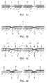
- FIGS. 1A to 1Hare sectional views at the respective steps of a method for manufacturing a semiconductor device according to an embodiment of the present invention
- FIGS. 2A and 2Bare sectional views of gate electrode portions of a memory cell transistor and a peripheral transistor in the semiconductor device of the present invention
- FIGS. 3A and 3Bare a sectional view and a plan view, of a peripheral transistor in a semiconductor device manufactured by a method according to a second embodiment of the present invention.
- FIG. 4shows a section of a peripheral transistor according to a third embodiment of the present invention.
- FIGS. 1A through 1Hmethod for manufacturing an EEPROM (Electrically Erasable Read-Only Memory), according to a first embodiment of the present invention, will be described.
- the left-sided portionrepresents a memory cell transistor formed in the memory cell region, whereas the right-sided portion shows a MOS transistor (peripheral transistor) fabricated in the peripheral circuit region.
- MOS transistorperipheral transistor
- a field oxide film 2 having a thickness of an order of 500 nmis formed on a surface of a silicon substrate 1 by the LOCOS method to provide an element isolation region.
- a tunnel oxide film 3 having a thickness of an order of 10 to 12 nmis fabricated on the silicon substrate 1 at a memory cell region in an active region surrounded by the element isolation region made of the field oxide film 2 by way of the thermal oxidation method.
- a gate oxide film 4having a thickness of an order of 10 to 40 nm is formed on the silicon substrate 1 at a peripheral circuit region in the active region surrounded by the field oxide film 2 by the thermal oxidation method.
- the tunnel oxide film 3 and the gate oxide film 4may be formed in a reversed order or at the same time.
- a polycrystalline silicon film 5 having a substantially uniform thickness of an order of 150 nmis formed over the entire surface by the CVD method.
- phosphorusis introduced by the ion injection method into the polycrystalline silicon film 5 at an impurity concentration of an order of 1 ⁇ 10 18 to 1 ⁇ 10 19 atoms/cm 3 . It is undesired that the impurity concentration in the polycrystalline silicon film 5 exceeds the above impurity concentration, because the boundary condition between the tunnel oxide film 3 and the polycrystalline silicon film 5 in the memory cell region is deteriorated, so that electrons are no more uniformly injected into or extracted from the polycrystalline silicon film 5 serving as the floating gate. It should be noted that instead of phosphorous, arsenic ions may be injected.
- the polycrystalline silicon film 5 in the memory cell regionis patterned to form a floating gate.
- an ONO film (silicon oxide film/silicon nitride film/silicon oxide film) 6is formed over the entire surface by the CVD method.
- a thickness of each of the two silicon oxide film layers for constituting this ONO film 6is in an order of 10 nm
- a thickness of the silicon nitride filmis in an order of 20 nm
- an overall thickness of the ONO film 6is in an order of 30 nm.
- an etching treatmentis carried out, while using a photoresist (not shown) of a pattern covering the memory cell region as a mask, so as to remove wholly a portion of the ONO film 6 formed on the peripheral circuit region.
- a polycrystalline silicon film 7 having a uniform thickness of approximately 150 nmis fabricated over the entire surface by the CVD method.
- phosphorousis diffused into the polycrystalline silicon film 7 by way of the vapor phase diffusion method by performing the thermal treatment in a furnace in which oxyphosphorus chloride (POCl 3 : phosphoryl trichloride) is vapored.
- This phosphorous vapor phase diffusionis carried out until the impurity concentration of the polycrystalline silicon film 7 becomes an order of 1 ⁇ 10 20 to 1 ⁇ 10 21 atom/cm 3 so that the impurity concentration of the polycrystalline silicon film 7 becomes at least 10 times that of the polycrystalline silicon film 5 .
- phosphorousarsenic may be diffused.
- the impurity concentration of the polycrystalline silicon film 5becomes approximately 1 ⁇ 10 20 to 1 ⁇ 10 21 atoms/cm 3 .
- the ONO film 6 containing the silicon nitride film which has a low diffusion speed of phosphorousis interposed between the polycrystalline silicon films 5 and in the memory cell region. As a result, phosphorous does not diffuse through the ONO film 6 into the polycrystalline silicon film 5 in the memory cell region. Accordingly, the impurity concentration of the polycrystalline silicon film 5 in the memory cell region remains at an order of 1 ⁇ 10 18 to 1 ⁇ 10 19 atoms/cm 3 .
- this photoresistis patterned to a shape of a control gate 15 of the memory cell transistor 11 (see FIG. 2A ) in the memory cell region, and also a shape of a gate electrode 16 of a peripheral transistor 12 (see FIG. 2B ) in the peripheral circuit region. Then, by using the patterned photoresist as a mask, an anisotropic etching is carried out with respect to the polycrystalline silicon film 7 , the ONO film 6 , and the polycrystalline silicon film 5 .
- a floating gate made of the polycrystalline silicon film 5 , and a control gate made of the polycrystalline silicon film 7are fabricated in the memory cell region, whereas a gate electrode of the peripheral transistor, which is made of the polycrystalline silicon films 5 and 7 , is formed in the peripheral circuit region.
- phosphorousis introduced into the polycrystalline silicon film 5 at a relatively low concentration by way of the ion injection method and the ONO film 6 is left at least on the polycrystalline silicon film 5 of the memory cell region. Therefore, when phosphorous is introduced at a relatively high concentration into the polycrystalline silicon film 7 by way of the vapor phase diffusion method, the silicon nitride film of the ONO film 6 functions as a diffusion stopper of phosphorous. As a consequence, the impurity concentration of the polycrystalline silicon film 5 of the memory cell region can be maintained at a relatively low level, and further the impurity concentration of the polycrystalline silicon film 5 of the peripheral circuit region can be set to the relatively high level.
- the polycrystalline silicon films 5 , 7 forming the gate electrode of the peripheral transistor, and the polycrystalline silicon film 7 forming the control gate of the memory transistorhave substantially the same conductivity which is higher than the conductivity of the polycrystalline silicon film 5 forming the floating gate of the memory transistor. Also, since the polycrystalline silicon films 5 and 7 have essentially uniform sectional areas, each of the polycrystalline silicon films 5 , 7 forming the gate electrode of the peripheral transistor, and the polycrystalline silicon film 7 forming the control gate of the memory transistor have substantially the same resistance.
- the boundary between the tunnel oxide film 3 of the memory cell transistor 11 and the polycrystalline silicon film 5can be maintained at better condition, and furthermore, the resistance of the gate electrode of the peripheral transistor 12 can be made sufficiently low. As a result, it is possible to manufacture an EEPROM having high reliability and capable of operating at high speed.
- the ONO film 6 formed in the peripheral circuit regionis completely removed in the step of FIG. 1F .
- the ONO film 6 fabricated in the peripheral circuit regionmay be partially removed so as to retain its portion disposed at a region where the peripheral transistor is formed.
- the impurity concentration of the polycrystalline silicon film 5 of the peripheral circuit regioncan be set to a relatively high concentration.
- the film structure of the memory cell transistor 11 in the longitudinal directionis substantially identical to the film structure of the peripheral transistor 12 in the longitudinal direction, the workability can be advantageously improved in the step of forming the floating gate by applying anisotropic etching to the polycrystalline silicon film 7 , the ONO film 6 and the polycrystalline silicon film 5 .
- this embodimentmay be applied to such a case that, for instance, the selecting transistor selectively switching the memory cell transistor 11 in the EEPROM is fabricated at the same time with the memory cell transistor 11 .
- this embodimentmay be applied not only to manufacturing of the EEPROM, but also any nonvolatile semiconductor memory device such as an EPROM in which each of the memory cell transistor and other transistors than the memory cell transistor uses a two-layer polycrystalline silicon film structure.
- FIG. 3Ashows a section of a portion including the gate electrode of a peripheral transistor in a step of the method of manufacturing a semiconductor device according to the second embodiment of the present invention, i.e. a section along the line IIIA to IIIA′ in FIG. 3B , which is a plan view of the region including the peripheral transistor in the second embodiment.
- the second embodimentsubstantially the same steps as those in the first embodiment as shown in FIGS. 1A to 1E are carried out.
- the second embodimentis different from the first embodiment in the step of FIG. 1F .
- the ONO film disposed in the region where the peripheral transistor is formedhas been removed in the step of FIG. 1F .
- only a part of the ONO film disposed in the element-isolation region where the field oxide film 2 is formedis removed, while unremoving a part of the ONO film disposed in the region 23 as shown in FIG. 3B including the active region 21 where the peripheral transistor is formed by masking the region 23 .
- the second embodimenta part of the ONO film disposed on the first polycrystalline silicon film of the peripheral transistor and at an area substantially above the active region is unremoved in the step corresponding to FIG. 1F of the first embodiment.
- the impurity ionsare not introduced into a portion 5 a ( FIG. 3B ) of the polycrystalline silicon film 5 disposed on the active region so that the impurity concentration of the portion 5 a remains at a low level and its resistance remains at a high level.
- a portion 5 b of the polycrystalline silicon film 5 disposed over the field oxide film 5 and serving as a wiring of the gate electrodehas substantially the same impurity concentration as that of the polycrystalline silicon film 7 , resulting in a low resistance of the portion 5 b , which is effective to prevent the delay in operation of its circuit. Further, due to the same reason as that in the case of the tunnel oxide.
- 19indicates the source/drain region of a peripheral transistor
- 24 or 25indicates a contact hole for connecting the source/drain region to a wiring layer (not shown)
- 22indicates a contact hole for connecting the gate electrode of the peripheral transistor to a wiring layer (not shown).
- the impurityis introduced at a relatively low concentration into the first polycrystalline silicon film by ion-implantation and also the insulating film containing the silicon nitride film is left on the polycrystalline silicon film in the memory cell region, when phosphorous is introduced at a relatively high concentration into the second polycrystalline silicon film by way of the thermal diffusion method, the silicon nitride film functions as a stopper for diffusion of the impurity.
- the impurity concentration of the first polycrystalline silicon film of the memory cell regioncan be maintained at a relatively low level, and further the impurity concentration of the first polycrystalline silicon film of the peripheral transistor can be set to a relatively high level.
- the boundary between the tunnel oxide film (first insulating film) of the memory cell transistor formed in the memory cell region and the first polycrystalline silicon filmcan be maintained at better condition, and furthermore, the resistance of the gate electrode wiring of the MOS transistor formed in the peripheral region can be made sufficiently low. As a results it is possible to manufacture a nonvolatile semiconductor memory device having high reliability and capable of operating at high speed.
Landscapes
- Engineering & Computer Science (AREA)
- Manufacturing & Machinery (AREA)
- Physics & Mathematics (AREA)
- Condensed Matter Physics & Semiconductors (AREA)
- General Physics & Mathematics (AREA)
- Computer Hardware Design (AREA)
- Microelectronics & Electronic Packaging (AREA)
- Power Engineering (AREA)
- Non-Volatile Memory (AREA)
- Semiconductor Memories (AREA)
Abstract
Description
Claims (21)
Priority Applications (1)
| Application Number | Priority Date | Filing Date | Title |
|---|---|---|---|
| US11/958,708US7452774B2 (en) | 1995-09-29 | 2007-12-18 | Semiconductor device including transistor with composite gate structure and transistor with single gate structure, and method for manufacturing the same |
Applications Claiming Priority (9)
| Application Number | Priority Date | Filing Date | Title |
|---|---|---|---|
| JP7-276292 | 1995-09-29 | ||
| JP27629295 | 1995-09-29 | ||
| JP07-276292 | 1995-09-29 | ||
| US08/720,014US5925907A (en) | 1995-09-29 | 1996-09-27 | Semiconductor device including transistor with composite gate structure and transistor with single gate structure |
| US31725599A | 1999-05-24 | 1999-05-24 | |
| US09/706,810US6525370B1 (en) | 1995-09-29 | 2000-11-07 | Semiconductor device including transistor with composite gate structure and transistor with single gate structure and method for manufacturing the same |
| US10/118,039US6787844B2 (en) | 1995-09-29 | 2002-04-09 | Semiconductor device including transistor with composite gate structure and transistor with single gate structure, and method for manufacturing the same |
| US10/725,318US7312496B2 (en) | 1995-09-29 | 2003-12-02 | Semiconductor device including transistor with composite gate structure and transistor with single gate structure, and method for manufacturing the same |
| US11/958,708US7452774B2 (en) | 1995-09-29 | 2007-12-18 | Semiconductor device including transistor with composite gate structure and transistor with single gate structure, and method for manufacturing the same |
Related Parent Applications (1)
| Application Number | Title | Priority Date | Filing Date |
|---|---|---|---|
| US10/725,318DivisionUS7312496B2 (en) | 1995-09-29 | 2003-12-02 | Semiconductor device including transistor with composite gate structure and transistor with single gate structure, and method for manufacturing the same |
Publications (2)
| Publication Number | Publication Date |
|---|---|
| US20080111179A1 US20080111179A1 (en) | 2008-05-15 |
| US7452774B2true US7452774B2 (en) | 2008-11-18 |
Family
ID=27336335
Family Applications (7)
| Application Number | Title | Priority Date | Filing Date |
|---|---|---|---|
| US10/118,039Expired - LifetimeUS6787844B2 (en) | 1995-09-29 | 2002-04-09 | Semiconductor device including transistor with composite gate structure and transistor with single gate structure, and method for manufacturing the same |
| US10/653,237Expired - Fee RelatedUS6913973B2 (en) | 1995-09-29 | 2003-09-03 | Semiconductor device including transistor with composite gate structure and transistor with single gate structure, and method for manufacturing the same |
| US10/725,318Expired - Fee RelatedUS7312496B2 (en) | 1995-09-29 | 2003-12-02 | Semiconductor device including transistor with composite gate structure and transistor with single gate structure, and method for manufacturing the same |
| US11/494,296Expired - Fee RelatedUS7439573B2 (en) | 1995-09-29 | 2006-07-27 | Semiconductor device including transistor with composite gate structure and transistor with single gate structure, and method for manufacturing the same |
| US11/494,261Expired - Fee RelatedUS7683423B2 (en) | 1995-09-29 | 2006-07-27 | Semiconductor device including transistor with composite gate structure and transistor with single gate structure, and method for manufacturing the same |
| US11/958,708Expired - Fee RelatedUS7452774B2 (en) | 1995-09-29 | 2007-12-18 | Semiconductor device including transistor with composite gate structure and transistor with single gate structure, and method for manufacturing the same |
| US12/254,683Expired - Fee RelatedUS7759195B2 (en) | 1995-09-29 | 2008-10-20 | Semiconductor device including transistor with composite gate structure and transistor with single gate structure, and method for manufacturing the same |
Family Applications Before (5)
| Application Number | Title | Priority Date | Filing Date |
|---|---|---|---|
| US10/118,039Expired - LifetimeUS6787844B2 (en) | 1995-09-29 | 2002-04-09 | Semiconductor device including transistor with composite gate structure and transistor with single gate structure, and method for manufacturing the same |
| US10/653,237Expired - Fee RelatedUS6913973B2 (en) | 1995-09-29 | 2003-09-03 | Semiconductor device including transistor with composite gate structure and transistor with single gate structure, and method for manufacturing the same |
| US10/725,318Expired - Fee RelatedUS7312496B2 (en) | 1995-09-29 | 2003-12-02 | Semiconductor device including transistor with composite gate structure and transistor with single gate structure, and method for manufacturing the same |
| US11/494,296Expired - Fee RelatedUS7439573B2 (en) | 1995-09-29 | 2006-07-27 | Semiconductor device including transistor with composite gate structure and transistor with single gate structure, and method for manufacturing the same |
| US11/494,261Expired - Fee RelatedUS7683423B2 (en) | 1995-09-29 | 2006-07-27 | Semiconductor device including transistor with composite gate structure and transistor with single gate structure, and method for manufacturing the same |
Family Applications After (1)
| Application Number | Title | Priority Date | Filing Date |
|---|---|---|---|
| US12/254,683Expired - Fee RelatedUS7759195B2 (en) | 1995-09-29 | 2008-10-20 | Semiconductor device including transistor with composite gate structure and transistor with single gate structure, and method for manufacturing the same |
Country Status (1)
| Country | Link |
|---|---|
| US (7) | US6787844B2 (en) |
Cited By (2)
| Publication number | Priority date | Publication date | Assignee | Title |
|---|---|---|---|---|
| US20070045714A1 (en)* | 1995-09-29 | 2007-03-01 | Katsuki Hazama | Semiconductor device including transistor with composite gate structure and transistor with single gate structure, and method for manufacturing the same |
| US20090090954A1 (en)* | 1997-09-20 | 2009-04-09 | Semiconductor Energy Laboratory Co., Ltd. | Nonvolatile memory and manufacturing method thereof |
Families Citing this family (22)
| Publication number | Priority date | Publication date | Assignee | Title |
|---|---|---|---|---|
| US8940645B2 (en) | 2007-05-25 | 2015-01-27 | Cypress Semiconductor Corporation | Radical oxidation process for fabricating a nonvolatile charge trap memory device |
| US8063434B1 (en) | 2007-05-25 | 2011-11-22 | Cypress Semiconductor Corporation | Memory transistor with multiple charge storing layers and a high work function gate electrode |
| US9449831B2 (en) | 2007-05-25 | 2016-09-20 | Cypress Semiconductor Corporation | Oxide-nitride-oxide stack having multiple oxynitride layers |
| US20090179253A1 (en) | 2007-05-25 | 2009-07-16 | Cypress Semiconductor Corporation | Oxide-nitride-oxide stack having multiple oxynitride layers |
| US8633537B2 (en) | 2007-05-25 | 2014-01-21 | Cypress Semiconductor Corporation | Memory transistor with multiple charge storing layers and a high work function gate electrode |
| EP2320454A1 (en)* | 2009-11-05 | 2011-05-11 | S.O.I.Tec Silicon on Insulator Technologies | Substrate holder and clipping device |
| US8508289B2 (en)* | 2009-12-08 | 2013-08-13 | Soitec | Data-path cell on an SeOI substrate with a back control gate beneath the insulating layer |
| FR2953643B1 (en)* | 2009-12-08 | 2012-07-27 | Soitec Silicon On Insulator | MEMORY CELL FLASH ON SEOI HAVING A SECOND CHECK GRID ENTERREE UNDER THE INSULATING LAYER |
| FR2953636B1 (en)* | 2009-12-08 | 2012-02-10 | Soitec Silicon On Insulator | METHOD FOR CONTROLLING A DRAM MEMORY CELL ON SEOI HAVING A SECOND BURST CONTROL GRID UNDER THE INSULATING LAYER |
| FR2953641B1 (en)* | 2009-12-08 | 2012-02-10 | S O I Tec Silicon On Insulator Tech | HOMOGENEOUS TRANSISTOR CIRCUIT ON SEOI WITH REAR CONTROL CHANNEL BURED UNDER THE INSULATING LAYER |
| FR2957193B1 (en)* | 2010-03-03 | 2012-04-20 | Soitec Silicon On Insulator | SEOI SUBSTRATE DATA PATH CELL WITH REAR CONTROL GRID BURED UNDER THE INSULATING LAYER |
| FR2955195B1 (en)* | 2010-01-14 | 2012-03-09 | Soitec Silicon On Insulator | DEVICE FOR COMPARING DATA IN A MEMORY ADDRESSABLE BY CONTENT ON SEOI |
| FR2955204B1 (en)* | 2010-01-14 | 2012-07-20 | Soitec Silicon On Insulator | DRAM MEMORY CELL HAVING A VERTICAL BIPOLAR INJECTOR |
| FR2955203B1 (en) | 2010-01-14 | 2012-03-23 | Soitec Silicon On Insulator | MEMORY CELL WITH THE CHANNEL CROSSING A DIELECTRIC LAYER ENTERREE |
| FR2955200B1 (en)* | 2010-01-14 | 2012-07-20 | Soitec Silicon On Insulator | DEVICE AND MANUFACTURING METHOD HAVING CONTACT BETWEEN SEMICONDUCTOR REGIONS THROUGH AN INSULATED INSULATED LAYER |
| FR2957186B1 (en)* | 2010-03-08 | 2012-09-28 | Soitec Silicon On Insulator | MEMORY CELL OF SRAM TYPE |
| FR2957449B1 (en) | 2010-03-11 | 2022-07-15 | S O I Tec Silicon On Insulator Tech | READOUT MICRO-AMPLIFIER FOR MEMORY |
| FR2958441B1 (en) | 2010-04-02 | 2012-07-13 | Soitec Silicon On Insulator | PSEUDO-INVERTER CIRCUIT ON SEOI |
| EP2375442A1 (en) | 2010-04-06 | 2011-10-12 | S.O.I.Tec Silicon on Insulator Technologies | Method for manufacturing a semiconductor substrate |
| EP2381470B1 (en)* | 2010-04-22 | 2012-08-22 | Soitec | Semiconductor device comprising a field-effect transistor in a silicon-on-insulator structure |
| US8685813B2 (en) | 2012-02-15 | 2014-04-01 | Cypress Semiconductor Corporation | Method of integrating a charge-trapping gate stack into a CMOS flow |
| KR101604977B1 (en)* | 2015-02-24 | 2016-03-22 | 주식회사 아바코 | Reactive sputtering apparatus |
Citations (34)
| Publication number | Priority date | Publication date | Assignee | Title |
|---|---|---|---|---|
| US4210993A (en) | 1975-09-17 | 1980-07-08 | Hitachi, Ltd. | Method for fabricating a field effect transistor |
| US4348746A (en) | 1979-03-30 | 1982-09-07 | Nippon Electric Co., Ltd. | Semiconductor integrated circuit device having a plurality of insulated gate field effect transistors |
| JPS5974677A (en) | 1982-10-22 | 1984-04-27 | Ricoh Co Ltd | Semiconductor device and its manufacturing method |
| US4453388A (en) | 1982-09-20 | 1984-06-12 | General Motors Corporation | Locking fuel cap |
| US4597159A (en) | 1984-03-09 | 1986-07-01 | Kabushiki Kaisha Toshiba | Method of manufacturing SiO2 -Si interface for floating gate semiconductor device |
| US4703551A (en) | 1986-01-24 | 1987-11-03 | Ncr Corporation | Process for forming LDD MOS/CMOS structures |
| JPH021176A (en) | 1988-03-18 | 1990-01-05 | Toshiba Corp | Nonvolatile semiconductor memory device and its manufacturing method |
| JPH023289A (en) | 1988-06-17 | 1990-01-08 | Sanyo Electric Co Ltd | Nonvolatile memory element and its manufacture |
| US4894802A (en) | 1988-02-02 | 1990-01-16 | Catalyst Semiconductor, Inc. | Nonvolatile memory cell for eeprom including a floating gate to drain tunnel area positioned away from the channel region to prevent trapping of electrons in the gate oxide during cell erase |
| US4958321A (en) | 1988-09-22 | 1990-09-18 | Advanced Micro Devices, Inc. | One transistor flash EPROM cell |
| US5034798A (en) | 1987-07-31 | 1991-07-23 | Kabushiki Kaisha Toshiba | Semiconductor device having a two-layer gate structure |
| JPH0548046A (en) | 1991-08-12 | 1993-02-26 | Fujitsu Ltd | Method for manufacturing semiconductor device |
| US5200636A (en) | 1989-10-11 | 1993-04-06 | Kabushiki Kaisha Toshiba | Semiconductor device having E2 PROM and EPROM in one chip |
| US5229631A (en) | 1990-08-15 | 1993-07-20 | Intel Corporation | Erase performance improvement via dual floating gate processing |
| EP0581312A1 (en) | 1992-07-31 | 1994-02-02 | Samsung Electronics Co., Ltd. | Non-volatile memory device and method of its manufacture |
| US5321287A (en) | 1989-10-06 | 1994-06-14 | Kabushiki Kaisha Toshiba | Semiconductor device wherein n-channel MOSFET, p-channel MOSFET and nonvolatile memory cell are formed in one chip |
| JPH06268213A (en) | 1993-03-16 | 1994-09-22 | Semiconductor Energy Lab Co Ltd | Insulated gate type field effect semiconductor device and manufacturing method thereof |
| JPH07183411A (en) | 1993-11-09 | 1995-07-21 | Sony Corp | Laminated-gate type nonvolatile semiconductor memory device |
| US5449629A (en) | 1991-11-14 | 1995-09-12 | Fujitsu Limited | Method for fabricating a semiconductor memory device having a floating gate with improved insulation film quality |
| US5470771A (en) | 1989-04-28 | 1995-11-28 | Nippondenso Co., Ltd. | Method of manufacturing a floating gate memory device |
| US5493139A (en) | 1993-05-27 | 1996-02-20 | Sharp Kabushiki Kaisha | Electrically erasable PROM (E2 PROM) with thin film peripheral transistor |
| US5541876A (en) | 1994-06-01 | 1996-07-30 | United Microelectronics Corporation | Memory cell fabricated by floating gate structure |
| JPH09153601A (en) | 1995-09-29 | 1997-06-10 | Nippon Steel Corp | Semiconductor device and manufacture thereof |
| US5637897A (en) | 1995-03-06 | 1997-06-10 | Nec Corporation | Nonvolatile semiconductor memory device with dual insulation layers between adjacent gate structures |
| US5691561A (en) | 1994-02-18 | 1997-11-25 | Fujitsu Limited | Semiconductor device and method for manufacturing semiconductor device |
| US5793673A (en) | 1993-02-19 | 1998-08-11 | Sgs-Thomson Microelectronics S.R.L. | Double polysilicon EEPROM cell and corresponding manufacturing process and programming method |
| US5925907A (en) | 1995-09-29 | 1999-07-20 | Nippon Steel Corporaition | Semiconductor device including transistor with composite gate structure and transistor with single gate structure |
| US6103576A (en) | 1999-04-13 | 2000-08-15 | Microchip Technology Incorporated | Dielectric layer of a memory cell having a stacked oxide sidewall and method of fabricating same |
| US6121670A (en) | 1996-07-30 | 2000-09-19 | Nec Corporation | Single-chip contact-less read-only memory (ROM) device and the method for fabricating the device |
| US6157575A (en) | 1998-03-26 | 2000-12-05 | Samsung Electronics Co., Ltd | Nonvolatile memory device and operating method thereof |
| US6365457B1 (en) | 1998-03-26 | 2002-04-02 | Samsung Electronics Co., Ltd. | Method for manufacturing nonvolatile memory device using self-aligned source process |
| US6417086B1 (en) | 1999-02-22 | 2002-07-09 | Kabushiki Kaisha Toshiba | Method of manufacturing semiconductor device having nonvolatile memory and logic circuit using multi-layered, inorganic mask |
| US6451643B2 (en) | 1988-11-09 | 2002-09-17 | Hitachi, Ltd. | Method of manufacturing a semiconductor device having non-volatile memory cell portion with single transistor type memory cells and peripheral portion with MISFETs |
| US6787844B2 (en) | 1995-09-29 | 2004-09-07 | Nippon Steel Corporation | Semiconductor device including transistor with composite gate structure and transistor with single gate structure, and method for manufacturing the same |
Family Cites Families (20)
| Publication number | Priority date | Publication date | Assignee | Title |
|---|---|---|---|---|
| US554876A (en)* | 1896-02-18 | Wrapper or holder for apparel | ||
| CH599302A5 (en) | 1973-06-21 | 1978-05-31 | Ciba Geigy Ag | |
| DE3037744A1 (en)* | 1980-10-06 | 1982-05-19 | Siemens AG, 1000 Berlin und 8000 München | METHOD FOR PRODUCING A MONOLITHICALLY INTEGRATED TWO-TRANSISTOR MEMORY CELL IN MOS TECHNOLOGY |
| US5834793A (en)* | 1985-12-27 | 1998-11-10 | Kabushiki Kaisha Toshiba | Semiconductor devices |
| JPH02201968A (en) | 1989-01-30 | 1990-08-10 | Kawasaki Steel Corp | Manufacture of semiconductor device |
| JPH02295170A (en) | 1989-05-09 | 1990-12-06 | Hitachi Ltd | Manufacture of semiconductor integrated circuit device |
| JPH03283570A (en) | 1990-03-30 | 1991-12-13 | Fujitsu Ltd | Semiconductor device and its production |
| US5317179A (en) | 1991-09-23 | 1994-05-31 | Integrated Silicon Solution, Inc. | Non-volatile semiconductor memory cell |
| JPH05299578A (en)* | 1992-04-17 | 1993-11-12 | Rohm Co Ltd | Semiconductor device and manufacture thereof |
| JPH0669515A (en)* | 1992-08-19 | 1994-03-11 | Fujitsu Ltd | Semiconductor memory device |
| JPH06125090A (en) | 1992-10-14 | 1994-05-06 | Seiko Epson Corp | Semiconductor device |
| JPH06151770A (en) | 1992-11-16 | 1994-05-31 | Mitsubishi Electric Corp | Manufacture of semiconductor memory |
| JP3405567B2 (en) | 1993-06-08 | 2003-05-12 | 株式会社東芝 | Nonvolatile semiconductor memory device |
| JPH06350099A (en) | 1993-06-08 | 1994-12-22 | Toshiba Corp | Semiconductor memory |
| JPH07115144A (en) | 1993-10-15 | 1995-05-02 | Sony Corp | Semiconductor non-volatile memory device |
| JPH0817949A (en) | 1994-03-25 | 1996-01-19 | Nippon Steel Corp | Nonvolatile semiconductor memory device and method of manufacturing the same |
| JP2590746B2 (en)* | 1994-07-29 | 1997-03-12 | 日本電気株式会社 | Method for manufacturing semiconductor device |
| JP5099983B2 (en) | 1995-09-29 | 2012-12-19 | インタレクチュアル ヴェンチャーズ ファースト エルエルシー | Semiconductor device and manufacturing method thereof |
| JP3383140B2 (en)* | 1995-10-02 | 2003-03-04 | 株式会社東芝 | Manufacturing method of nonvolatile semiconductor memory device |
| JP2002243912A (en) | 2001-02-14 | 2002-08-28 | Sony Corp | Lens, doublet, manufacturing method, optical pickup device, and optical disk device |
- 2002
- 2002-04-09USUS10/118,039patent/US6787844B2/ennot_activeExpired - Lifetime
- 2003
- 2003-09-03USUS10/653,237patent/US6913973B2/ennot_activeExpired - Fee Related
- 2003-12-02USUS10/725,318patent/US7312496B2/ennot_activeExpired - Fee Related
- 2006
- 2006-07-27USUS11/494,296patent/US7439573B2/ennot_activeExpired - Fee Related
- 2006-07-27USUS11/494,261patent/US7683423B2/ennot_activeExpired - Fee Related
- 2007
- 2007-12-18USUS11/958,708patent/US7452774B2/ennot_activeExpired - Fee Related
- 2008
- 2008-10-20USUS12/254,683patent/US7759195B2/ennot_activeExpired - Fee Related
Patent Citations (40)
| Publication number | Priority date | Publication date | Assignee | Title |
|---|---|---|---|---|
| US4210993A (en) | 1975-09-17 | 1980-07-08 | Hitachi, Ltd. | Method for fabricating a field effect transistor |
| US4348746A (en) | 1979-03-30 | 1982-09-07 | Nippon Electric Co., Ltd. | Semiconductor integrated circuit device having a plurality of insulated gate field effect transistors |
| US4453388A (en) | 1982-09-20 | 1984-06-12 | General Motors Corporation | Locking fuel cap |
| US4766088A (en) | 1982-10-22 | 1988-08-23 | Ricoh Company, Ltd. | Method of making a memory device with polysilicon electrodes |
| JPS5974677A (en) | 1982-10-22 | 1984-04-27 | Ricoh Co Ltd | Semiconductor device and its manufacturing method |
| US4597159A (en) | 1984-03-09 | 1986-07-01 | Kabushiki Kaisha Toshiba | Method of manufacturing SiO2 -Si interface for floating gate semiconductor device |
| US4703551A (en) | 1986-01-24 | 1987-11-03 | Ncr Corporation | Process for forming LDD MOS/CMOS structures |
| US5034798A (en) | 1987-07-31 | 1991-07-23 | Kabushiki Kaisha Toshiba | Semiconductor device having a two-layer gate structure |
| US4894802A (en) | 1988-02-02 | 1990-01-16 | Catalyst Semiconductor, Inc. | Nonvolatile memory cell for eeprom including a floating gate to drain tunnel area positioned away from the channel region to prevent trapping of electrons in the gate oxide during cell erase |
| JPH021176A (en) | 1988-03-18 | 1990-01-05 | Toshiba Corp | Nonvolatile semiconductor memory device and its manufacturing method |
| JPH023289A (en) | 1988-06-17 | 1990-01-08 | Sanyo Electric Co Ltd | Nonvolatile memory element and its manufacture |
| US4958321A (en) | 1988-09-22 | 1990-09-18 | Advanced Micro Devices, Inc. | One transistor flash EPROM cell |
| US6451643B2 (en) | 1988-11-09 | 2002-09-17 | Hitachi, Ltd. | Method of manufacturing a semiconductor device having non-volatile memory cell portion with single transistor type memory cells and peripheral portion with MISFETs |
| US5470771A (en) | 1989-04-28 | 1995-11-28 | Nippondenso Co., Ltd. | Method of manufacturing a floating gate memory device |
| US5321287A (en) | 1989-10-06 | 1994-06-14 | Kabushiki Kaisha Toshiba | Semiconductor device wherein n-channel MOSFET, p-channel MOSFET and nonvolatile memory cell are formed in one chip |
| US5200636A (en) | 1989-10-11 | 1993-04-06 | Kabushiki Kaisha Toshiba | Semiconductor device having E2 PROM and EPROM in one chip |
| US5229631A (en) | 1990-08-15 | 1993-07-20 | Intel Corporation | Erase performance improvement via dual floating gate processing |
| JPH0548046A (en) | 1991-08-12 | 1993-02-26 | Fujitsu Ltd | Method for manufacturing semiconductor device |
| US5449629A (en) | 1991-11-14 | 1995-09-12 | Fujitsu Limited | Method for fabricating a semiconductor memory device having a floating gate with improved insulation film quality |
| EP0581312A1 (en) | 1992-07-31 | 1994-02-02 | Samsung Electronics Co., Ltd. | Non-volatile memory device and method of its manufacture |
| US5793673A (en) | 1993-02-19 | 1998-08-11 | Sgs-Thomson Microelectronics S.R.L. | Double polysilicon EEPROM cell and corresponding manufacturing process and programming method |
| JPH06268213A (en) | 1993-03-16 | 1994-09-22 | Semiconductor Energy Lab Co Ltd | Insulated gate type field effect semiconductor device and manufacturing method thereof |
| US5493139A (en) | 1993-05-27 | 1996-02-20 | Sharp Kabushiki Kaisha | Electrically erasable PROM (E2 PROM) with thin film peripheral transistor |
| JPH07183411A (en) | 1993-11-09 | 1995-07-21 | Sony Corp | Laminated-gate type nonvolatile semiconductor memory device |
| US5691561A (en) | 1994-02-18 | 1997-11-25 | Fujitsu Limited | Semiconductor device and method for manufacturing semiconductor device |
| US5541876A (en) | 1994-06-01 | 1996-07-30 | United Microelectronics Corporation | Memory cell fabricated by floating gate structure |
| US5637897A (en) | 1995-03-06 | 1997-06-10 | Nec Corporation | Nonvolatile semiconductor memory device with dual insulation layers between adjacent gate structures |
| US6913973B2 (en) | 1995-09-29 | 2005-07-05 | Nippon Steel Corporation | Semiconductor device including transistor with composite gate structure and transistor with single gate structure, and method for manufacturing the same |
| JPH09153601A (en) | 1995-09-29 | 1997-06-10 | Nippon Steel Corp | Semiconductor device and manufacture thereof |
| US5925907A (en) | 1995-09-29 | 1999-07-20 | Nippon Steel Corporaition | Semiconductor device including transistor with composite gate structure and transistor with single gate structure |
| US7312496B2 (en)* | 1995-09-29 | 2007-12-25 | Pegre Semiconductors, Llc | Semiconductor device including transistor with composite gate structure and transistor with single gate structure, and method for manufacturing the same |
| US20070045714A1 (en) | 1995-09-29 | 2007-03-01 | Katsuki Hazama | Semiconductor device including transistor with composite gate structure and transistor with single gate structure, and method for manufacturing the same |
| US20070029596A1 (en) | 1995-09-29 | 2007-02-08 | Katsuki Hazama | Semiconductor device including transistor with composite gate structure and transistor with single gate structure, and method for manufacturing the same |
| US6525370B1 (en) | 1995-09-29 | 2003-02-25 | Nippon Steel Corporation | Semiconductor device including transistor with composite gate structure and transistor with single gate structure and method for manufacturing the same |
| US6787844B2 (en) | 1995-09-29 | 2004-09-07 | Nippon Steel Corporation | Semiconductor device including transistor with composite gate structure and transistor with single gate structure, and method for manufacturing the same |
| US6121670A (en) | 1996-07-30 | 2000-09-19 | Nec Corporation | Single-chip contact-less read-only memory (ROM) device and the method for fabricating the device |
| US6365457B1 (en) | 1998-03-26 | 2002-04-02 | Samsung Electronics Co., Ltd. | Method for manufacturing nonvolatile memory device using self-aligned source process |
| US6157575A (en) | 1998-03-26 | 2000-12-05 | Samsung Electronics Co., Ltd | Nonvolatile memory device and operating method thereof |
| US6417086B1 (en) | 1999-02-22 | 2002-07-09 | Kabushiki Kaisha Toshiba | Method of manufacturing semiconductor device having nonvolatile memory and logic circuit using multi-layered, inorganic mask |
| US6103576A (en) | 1999-04-13 | 2000-08-15 | Microchip Technology Incorporated | Dielectric layer of a memory cell having a stacked oxide sidewall and method of fabricating same |
Cited By (6)
| Publication number | Priority date | Publication date | Assignee | Title |
|---|---|---|---|---|
| US20070045714A1 (en)* | 1995-09-29 | 2007-03-01 | Katsuki Hazama | Semiconductor device including transistor with composite gate structure and transistor with single gate structure, and method for manufacturing the same |
| US20090047763A1 (en)* | 1995-09-29 | 2009-02-19 | Katsuki Hazama | Semiconductor device including transistor with composite gate structure and transistor with single gate structure, and method for manufacturing the same |
| US7683423B2 (en) | 1995-09-29 | 2010-03-23 | Katsuki Hazama | Semiconductor device including transistor with composite gate structure and transistor with single gate structure, and method for manufacturing the same |
| US7759195B2 (en) | 1995-09-29 | 2010-07-20 | Katsuki Hazama | Semiconductor device including transistor with composite gate structure and transistor with single gate structure, and method for manufacturing the same |
| US20090090954A1 (en)* | 1997-09-20 | 2009-04-09 | Semiconductor Energy Laboratory Co., Ltd. | Nonvolatile memory and manufacturing method thereof |
| US7989873B2 (en) | 1997-09-20 | 2011-08-02 | Semiconductor Energy Laboratory Co., Ltd. | Nonvolatile memory and manufacturing method thereof |
Also Published As
| Publication number | Publication date |
|---|---|
| US20040104423A1 (en) | 2004-06-03 |
| US6913973B2 (en) | 2005-07-05 |
| US7312496B2 (en) | 2007-12-25 |
| US6787844B2 (en) | 2004-09-07 |
| US20070045714A1 (en) | 2007-03-01 |
| US20040043564A1 (en) | 2004-03-04 |
| US7683423B2 (en) | 2010-03-23 |
| US20070029596A1 (en) | 2007-02-08 |
| US7439573B2 (en) | 2008-10-21 |
| US20020137285A1 (en) | 2002-09-26 |
| US7759195B2 (en) | 2010-07-20 |
| US20090047763A1 (en) | 2009-02-19 |
| US20080111179A1 (en) | 2008-05-15 |
Similar Documents
| Publication | Publication Date | Title |
|---|---|---|
| US7452774B2 (en) | Semiconductor device including transistor with composite gate structure and transistor with single gate structure, and method for manufacturing the same | |
| KR960009995B1 (en) | Semiconductor device structure and manufacturing method thereof | |
| US6137134A (en) | Semiconductor memory device | |
| US5726470A (en) | Nonvolatile semiconductor memory device and method of fabrication of the same | |
| JP3124334B2 (en) | Semiconductor storage device and method of manufacturing the same | |
| US4517732A (en) | Method for fabricating an EEPROM | |
| US5962890A (en) | Non-volatile semiconductor memory | |
| US6417044B1 (en) | Non-volatile memory and memory of manufacturing the same | |
| JP2525144B2 (en) | Method of manufacturing integrated structure including non-volatile memory cell and related transistor | |
| US6171927B1 (en) | Device with differential field isolation thicknesses and related methods | |
| KR0146401B1 (en) | Method for manufacturing a semiconductor integrated circuit device having a stack gate structure | |
| KR100210999B1 (en) | A manufacturing method of a nonvolatile semiconductor memory having an erase gate | |
| US6525370B1 (en) | Semiconductor device including transistor with composite gate structure and transistor with single gate structure and method for manufacturing the same | |
| JPH08306889A (en) | Nonvolatile semiconductor memory device and method of manufacturing the same | |
| JP4057081B2 (en) | Method for manufacturing nonvolatile semiconductor memory device | |
| KR950011029B1 (en) | Manufacturing method of nonvolatile semiconductor memory device | |
| US6784057B2 (en) | Semiconductor device and nonvolatile semiconductor memory device comprising a plurality of semiconductor elements as well as process for the same | |
| KR0136531B1 (en) | Fabrication method of semiconductor device | |
| US6602774B1 (en) | Selective salicidation process for electronic devices integrated in a semiconductor substrate | |
| JP5099983B2 (en) | Semiconductor device and manufacturing method thereof | |
| US6320217B1 (en) | Semiconductor memory device | |
| KR900004731B1 (en) | Read only memory semiconductor device and manufacture thereof | |
| US6326267B1 (en) | Method of forming non-volatile semiconductor memory | |
| KR100358140B1 (en) | Flash memory manufacturing method | |
| KR19980073892A (en) | Method of manufacturing nonvolatile semiconductor memory device |
Legal Events
| Date | Code | Title | Description |
|---|---|---|---|
| AS | Assignment | Owner name:NIPPON STEEL CORPORATION, JAPAN Free format text:ASSIGNMENT OF ASSIGNORS INTEREST;ASSIGNOR:HAZAMA, KATSUKI;REEL/FRAME:020403/0891 Effective date:19960830 | |
| AS | Assignment | Owner name:PEGRE SEMICONDUCTORS LLC, NEVADA Free format text:ASSIGNMENT OF ASSIGNORS INTEREST;ASSIGNORS:NIPPON STEEL CORPORATION;NS SOLUTIONS CORPORATION;REEL/FRAME:020679/0422 Effective date:20051208 Owner name:PEGRE SEMICONDUCTORS LLC,NEVADA Free format text:ASSIGNMENT OF ASSIGNORS INTEREST;ASSIGNORS:NIPPON STEEL CORPORATION;NS SOLUTIONS CORPORATION;REEL/FRAME:020679/0422 Effective date:20051208 | |
| STCF | Information on status: patent grant | Free format text:PATENTED CASE | |
| AS | Assignment | Owner name:INTELLECTUAL VENTURES I LLC, DELAWARE Free format text:MERGER;ASSIGNOR:PEGRE SEMICONDUCTORS LLC;REEL/FRAME:025446/0042 Effective date:20101207 | |
| FPAY | Fee payment | Year of fee payment:4 | |
| FPAY | Fee payment | Year of fee payment:8 | |
| AS | Assignment | Owner name:HANGER SOLUTIONS, LLC, GEORGIA Free format text:ASSIGNMENT OF ASSIGNORS INTEREST;ASSIGNOR:INTELLECTUAL VENTURES ASSETS 161 LLC;REEL/FRAME:052159/0509 Effective date:20191206 | |
| AS | Assignment | Owner name:INTELLECTUAL VENTURES ASSETS 161 LLC, DELAWARE Free format text:ASSIGNMENT OF ASSIGNORS INTEREST;ASSIGNOR:INTELLECTUAL VENTURES I LLC;REEL/FRAME:051945/0001 Effective date:20191126 | |
| FEPP | Fee payment procedure | Free format text:MAINTENANCE FEE REMINDER MAILED (ORIGINAL EVENT CODE: REM.); ENTITY STATUS OF PATENT OWNER: LARGE ENTITY | |
| LAPS | Lapse for failure to pay maintenance fees | Free format text:PATENT EXPIRED FOR FAILURE TO PAY MAINTENANCE FEES (ORIGINAL EVENT CODE: EXP.); ENTITY STATUS OF PATENT OWNER: LARGE ENTITY | |
| STCH | Information on status: patent discontinuation | Free format text:PATENT EXPIRED DUE TO NONPAYMENT OF MAINTENANCE FEES UNDER 37 CFR 1.362 | |
| FP | Lapsed due to failure to pay maintenance fee | Effective date:20201118 |