US7452766B2 - Finned memory cells and the fabrication thereof - Google Patents
Finned memory cells and the fabrication thereofDownload PDFInfo
- Publication number
- US7452766B2 US7452766B2US11/514,004US51400406AUS7452766B2US 7452766 B2US7452766 B2US 7452766B2US 51400406 AUS51400406 AUS 51400406AUS 7452766 B2US7452766 B2US 7452766B2
- Authority
- US
- United States
- Prior art keywords
- fins
- conductive layer
- forming
- dielectric layer
- memory
- Prior art date
- Legal status (The legal status is an assumption and is not a legal conclusion. Google has not performed a legal analysis and makes no representation as to the accuracy of the status listed.)
- Active, expires
Links
- 238000004519manufacturing processMethods0.000titledescription9
- 239000000758substrateSubstances0.000claimsabstractdescription36
- 238000000034methodMethods0.000claimsabstractdescription20
- 238000002955isolationMethods0.000claimsdescription43
- 238000005530etchingMethods0.000claimsdescription12
- 239000000463materialSubstances0.000claimsdescription3
- 230000015572biosynthetic processEffects0.000claimsdescription2
- 238000007667floatingMethods0.000description57
- 239000003989dielectric materialSubstances0.000description10
- 239000004065semiconductorSubstances0.000description8
- 230000008021depositionEffects0.000description7
- 125000006850spacer groupChemical group0.000description7
- 229910021420polycrystalline siliconInorganic materials0.000description6
- 229920005591polysiliconPolymers0.000description6
- 239000000126substanceSubstances0.000description5
- 230000005669field effectEffects0.000description4
- 230000008569processEffects0.000description4
- 239000010936titaniumSubstances0.000description4
- 229910052581Si3N4Inorganic materials0.000description3
- 238000004891communicationMethods0.000description3
- 238000005516engineering processMethods0.000description3
- 229910052751metalInorganic materials0.000description3
- 239000002184metalSubstances0.000description3
- 238000005498polishingMethods0.000description3
- 238000000926separation methodMethods0.000description3
- HQVNEWCFYHHQES-UHFFFAOYSA-Nsilicon nitrideChemical compoundN12[Si]34N5[Si]62N3[Si]51N64HQVNEWCFYHHQES-UHFFFAOYSA-N0.000description3
- VYPSYNLAJGMNEJ-UHFFFAOYSA-NSilicium dioxideChemical compoundO=[Si]=OVYPSYNLAJGMNEJ-UHFFFAOYSA-N0.000description2
- RTAQQCXQSZGOHL-UHFFFAOYSA-NTitaniumChemical compound[Ti]RTAQQCXQSZGOHL-UHFFFAOYSA-N0.000description2
- 230000003213activating effectEffects0.000description2
- PNEYBMLMFCGWSK-UHFFFAOYSA-Naluminium oxideInorganic materials[O-2].[O-2].[O-2].[Al+3].[Al+3]PNEYBMLMFCGWSK-UHFFFAOYSA-N0.000description2
- 230000004888barrier functionEffects0.000description2
- 239000011651chromiumSubstances0.000description2
- 230000008878couplingEffects0.000description2
- 238000010168coupling processMethods0.000description2
- 238000005859coupling reactionMethods0.000description2
- 238000010586diagramMethods0.000description2
- 239000010955niobiumSubstances0.000description2
- 229920003209poly(hydridosilsesquioxane)Polymers0.000description2
- 239000003870refractory metalSubstances0.000description2
- 230000004044responseEffects0.000description2
- 230000003068static effectEffects0.000description2
- 229910052719titaniumInorganic materials0.000description2
- WFKWXMTUELFFGS-UHFFFAOYSA-NtungstenChemical compound[W]WFKWXMTUELFFGS-UHFFFAOYSA-N0.000description2
- 229910052721tungstenInorganic materials0.000description2
- 239000010937tungstenSubstances0.000description2
- VYZAMTAEIAYCRO-UHFFFAOYSA-NChromiumChemical compound[Cr]VYZAMTAEIAYCRO-UHFFFAOYSA-N0.000description1
- ZOKXTWBITQBERF-UHFFFAOYSA-NMolybdenumChemical compound[Mo]ZOKXTWBITQBERF-UHFFFAOYSA-N0.000description1
- XUIMIQQOPSSXEZ-UHFFFAOYSA-NSiliconChemical compound[Si]XUIMIQQOPSSXEZ-UHFFFAOYSA-N0.000description1
- NRTOMJZYCJJWKI-UHFFFAOYSA-NTitanium nitrideChemical compound[Ti]#NNRTOMJZYCJJWKI-UHFFFAOYSA-N0.000description1
- 229910052454barium strontium titanateInorganic materials0.000description1
- 239000003990capacitorSubstances0.000description1
- 229910052804chromiumInorganic materials0.000description1
- 239000010941cobaltSubstances0.000description1
- 229910017052cobaltInorganic materials0.000description1
- GUTLYIVDDKVIGB-UHFFFAOYSA-Ncobalt atomChemical compound[Co]GUTLYIVDDKVIGB-UHFFFAOYSA-N0.000description1
- 239000004020conductorSubstances0.000description1
- 238000010276constructionMethods0.000description1
- 229910052593corundumInorganic materials0.000description1
- 238000013500data storageMethods0.000description1
- 230000006870functionEffects0.000description1
- 229910052735hafniumInorganic materials0.000description1
- VBJZVLUMGGDVMO-UHFFFAOYSA-Nhafnium atomChemical compound[Hf]VBJZVLUMGGDVMO-UHFFFAOYSA-N0.000description1
- UQEAIHBTYFGYIE-UHFFFAOYSA-NhexamethyldisiloxaneChemical compoundC[Si](C)(C)O[Si](C)(C)CUQEAIHBTYFGYIE-UHFFFAOYSA-N0.000description1
- 239000012212insulatorSubstances0.000description1
- 150000002739metalsChemical class0.000description1
- 229910052750molybdenumInorganic materials0.000description1
- 239000011733molybdenumSubstances0.000description1
- 229910021421monocrystalline siliconInorganic materials0.000description1
- 229910052758niobiumInorganic materials0.000description1
- GUCVJGMIXFAOAE-UHFFFAOYSA-Nniobium atomChemical compound[Nb]GUCVJGMIXFAOAE-UHFFFAOYSA-N0.000description1
- CXQXSVUQTKDNFP-UHFFFAOYSA-NoctamethyltrisiloxaneChemical compoundC[Si](C)(C)O[Si](C)(C)O[Si](C)(C)CCXQXSVUQTKDNFP-UHFFFAOYSA-N0.000description1
- 230000003647oxidationEffects0.000description1
- 238000007254oxidation reactionMethods0.000description1
- TWNQGVIAIRXVLR-UHFFFAOYSA-Noxo(oxoalumanyloxy)alumaneChemical compoundO=[Al]O[Al]=OTWNQGVIAIRXVLR-UHFFFAOYSA-N0.000description1
- BPUBBGLMJRNUCC-UHFFFAOYSA-Noxygen(2-);tantalum(5+)Chemical compound[O-2].[O-2].[O-2].[O-2].[O-2].[Ta+5].[Ta+5]BPUBBGLMJRNUCC-UHFFFAOYSA-N0.000description1
- 238000000059patterningMethods0.000description1
- 229920001690polydopaminePolymers0.000description1
- 229910052594sapphireInorganic materials0.000description1
- 239000010980sapphireSubstances0.000description1
- VSZWPYCFIRKVQL-UHFFFAOYSA-Nselanylidenegallium;seleniumChemical compound[Se].[Se]=[Ga].[Se]=[Ga]VSZWPYCFIRKVQL-UHFFFAOYSA-N0.000description1
- 229910021332silicideInorganic materials0.000description1
- FVBUAEGBCNSCDD-UHFFFAOYSA-Nsilicide(4-)Chemical compound[Si-4]FVBUAEGBCNSCDD-UHFFFAOYSA-N0.000description1
- 229910052710siliconInorganic materials0.000description1
- 239000010703siliconSubstances0.000description1
- 235000012239silicon dioxideNutrition0.000description1
- 239000000377silicon dioxideSubstances0.000description1
- 239000007787solidSubstances0.000description1
- 229910052715tantalumInorganic materials0.000description1
- GUVRBAGPIYLISA-UHFFFAOYSA-Ntantalum atomChemical compound[Ta]GUVRBAGPIYLISA-UHFFFAOYSA-N0.000description1
- 229910001936tantalum oxideInorganic materials0.000description1
- 239000010409thin filmSubstances0.000description1
- LEONUFNNVUYDNQ-UHFFFAOYSA-Nvanadium atomChemical compound[V]LEONUFNNVUYDNQ-UHFFFAOYSA-N0.000description1
- 229910001845yogo sapphireInorganic materials0.000description1
Images


Classifications
- H—ELECTRICITY
- H10—SEMICONDUCTOR DEVICES; ELECTRIC SOLID-STATE DEVICES NOT OTHERWISE PROVIDED FOR
- H10D—INORGANIC ELECTRIC SEMICONDUCTOR DEVICES
- H10D30/00—Field-effect transistors [FET]
- H10D30/60—Insulated-gate field-effect transistors [IGFET]
- H10D30/68—Floating-gate IGFETs
- H10D30/6891—Floating-gate IGFETs characterised by the shapes, relative sizes or dispositions of the floating gate electrode
- H10D30/6894—Floating-gate IGFETs characterised by the shapes, relative sizes or dispositions of the floating gate electrode having one gate at least partly in a trench
- H—ELECTRICITY
- H10—SEMICONDUCTOR DEVICES; ELECTRIC SOLID-STATE DEVICES NOT OTHERWISE PROVIDED FOR
- H10B—ELECTRONIC MEMORY DEVICES
- H10B41/00—Electrically erasable-and-programmable ROM [EEPROM] devices comprising floating gates
- H10B41/30—Electrically erasable-and-programmable ROM [EEPROM] devices comprising floating gates characterised by the memory core region
- H—ELECTRICITY
- H10—SEMICONDUCTOR DEVICES; ELECTRIC SOLID-STATE DEVICES NOT OTHERWISE PROVIDED FOR
- H10D—INORGANIC ELECTRIC SEMICONDUCTOR DEVICES
- H10D30/00—Field-effect transistors [FET]
- H10D30/01—Manufacture or treatment
- H10D30/021—Manufacture or treatment of FETs having insulated gates [IGFET]
- H10D30/0411—Manufacture or treatment of FETs having insulated gates [IGFET] of FETs having floating gates
- H—ELECTRICITY
- H10—SEMICONDUCTOR DEVICES; ELECTRIC SOLID-STATE DEVICES NOT OTHERWISE PROVIDED FOR
- H10D—INORGANIC ELECTRIC SEMICONDUCTOR DEVICES
- H10D30/00—Field-effect transistors [FET]
- H10D30/60—Insulated-gate field-effect transistors [IGFET]
- H10D30/68—Floating-gate IGFETs
- H10D30/681—Floating-gate IGFETs having only two programming levels
- H—ELECTRICITY
- H10—SEMICONDUCTOR DEVICES; ELECTRIC SOLID-STATE DEVICES NOT OTHERWISE PROVIDED FOR
- H10D—INORGANIC ELECTRIC SEMICONDUCTOR DEVICES
- H10D64/00—Electrodes of devices having potential barriers
- H10D64/01—Manufacture or treatment
- H10D64/031—Manufacture or treatment of data-storage electrodes
- H10D64/035—Manufacture or treatment of data-storage electrodes comprising conductor-insulator-conductor-insulator-semiconductor structures
- H—ELECTRICITY
- H10—SEMICONDUCTOR DEVICES; ELECTRIC SOLID-STATE DEVICES NOT OTHERWISE PROVIDED FOR
- H10D—INORGANIC ELECTRIC SEMICONDUCTOR DEVICES
- H10D30/00—Field-effect transistors [FET]
- H10D30/01—Manufacture or treatment
- H10D30/021—Manufacture or treatment of FETs having insulated gates [IGFET]
- H10D30/024—Manufacture or treatment of FETs having insulated gates [IGFET] of fin field-effect transistors [FinFET]
- H10D30/0245—Manufacture or treatment of FETs having insulated gates [IGFET] of fin field-effect transistors [FinFET] by further thinning the channel after patterning the channel, e.g. using sacrificial oxidation on fins
- H—ELECTRICITY
- H10—SEMICONDUCTOR DEVICES; ELECTRIC SOLID-STATE DEVICES NOT OTHERWISE PROVIDED FOR
- H10D—INORGANIC ELECTRIC SEMICONDUCTOR DEVICES
- H10D30/00—Field-effect transistors [FET]
- H10D30/60—Insulated-gate field-effect transistors [IGFET]
- H10D30/62—Fin field-effect transistors [FinFET]
- H10D30/6211—Fin field-effect transistors [FinFET] having fin-shaped semiconductor bodies integral with the bulk semiconductor substrates
- H—ELECTRICITY
- H10—SEMICONDUCTOR DEVICES; ELECTRIC SOLID-STATE DEVICES NOT OTHERWISE PROVIDED FOR
- H10D—INORGANIC ELECTRIC SEMICONDUCTOR DEVICES
- H10D30/00—Field-effect transistors [FET]
- H10D30/60—Insulated-gate field-effect transistors [IGFET]
- H10D30/62—Fin field-effect transistors [FinFET]
- H10D30/6212—Fin field-effect transistors [FinFET] having fin-shaped semiconductor bodies having non-rectangular cross-sections
- H10D30/6213—Fin field-effect transistors [FinFET] having fin-shaped semiconductor bodies having non-rectangular cross-sections having rounded corners
Definitions
- the present disclosurerelates generally to memory devices and in particular the present invention relates to finned memory cells and the fabrication thereof.
- Memory devicesare typically provided as internal storage areas in computers.
- the term memoryidentifies data storage that comes in the form of integrated circuit chips.
- memory devicescontain an array of memory cells for storing data, and row and column decoder circuits coupled to the array of memory cells for accessing the array of memory cells in response to an external address.
- flash memoryis a non-volatile memory known as flash memory.
- a flash memoryis a type of EEPROM (electrically-erasable programmable read-only memory) that can be erased and reprogrammed in blocks.
- PCspersonal computers
- BIOSstored on a flash memory chip so that it can easily be updated if necessary.
- BIOSis sometimes called a flash BIOS. Flash memory is also popular in wireless electronic devices because it enables the manufacturer to support new communication protocols as they become standardized and to provide the ability to remotely upgrade the device for enhanced features.
- a typical flash memorycomprises a memory array that includes a large number of memory cells arranged in row and column fashion.
- Each of the memory cellsincludes a floating-gate field-effect transistor capable of holding a charge.
- the cellsare usually grouped into blocks.
- Each of the cells within a blockcan be electrically programmed on an individual basis by charging the floating gate.
- the chargecan be removed from the floating gate by a block erase operation.
- the data in a cellis determined by the presence or absence of the charge on the floating gate.
- NOR and NAND flash memory devicesare two common types of flash memory devices, so called for the logical form of the basic memory cell configuration in which each is arranged.
- the control gate of each memory cell of a row of the arrayis connected to a word line
- the drain region of each memory cell of a column of the arrayis connected to a bit line.
- the memory array for NOR flash memory devicesis accessed by a row decoder activating a row of floating-gate memory cells by selecting the word line coupled to their gates.
- the row of selected memory cellsthen place their data values on the column bit lines by flowing a differing current, depending upon their programmed states, from a coupled source line to the coupled column bit lines.
- the array of memory cells for NAND flash memory devicesis also arranged such that the control gate of each memory cell of a row of the array is connected to a word line.
- each memory cellis not directly coupled to a column bit line by its drain region. Instead, the memory cells of the array are arranged together in strings (often termed NAND strings), typically of 32 each, with the memory cells coupled together in series, source to drain, between a source line and a column bit line.
- the memory array for NAND flash memory devicesis then accessed by a row decoder activating a row of memory cells by selecting the word line coupled to a control gate of a memory cell.
- the word lines coupled to the control gates of unselected memory cells of each stringare driven to operate the unselected memory cells of each string as pass transistors, so that they pass current in a manner that is unrestricted by their stored data values.
- Currentthen flows from the source line to the column bit line through each series coupled string, restricted only by the selected memory cells of each string. This places the current-encoded data values of the row of selected memory cells on the column bit lines.
- FinFet deviceshaving a channel formed on an elongated protrusion (or a fin) formed in a substrate, increase cell currents and have improved cut-off characteristics compared to conventional memory cells, but generally have poorer coupling ratios than conventional memory cells.
- FIG. 1is a block diagram illustration of an integrated circuit device, according to an embodiment of the disclosure.
- FIG. 2is a schematic of a NAND memory array in accordance with another embodiment of the disclosure.
- FIG. 3is an illustration of an exemplary memory module, according to another embodiment of the disclosure.
- FIGS. 4A-4Jare cross-sectional views of a portion of a row of a memory array during various stages of fabrication, according to another embodiment of the disclosure.
- FIG. 5is a cross-sectional view of a portion of a row of a memory array, according to another embodiment of the disclosure.
- FIGS. 6A-6Fare cross-sectional views of a portion of a row of a memory array during various stages of fabrication, according to another embodiment of the disclosure.
- FIG. 7is a cross-sectional view of a portion of a row of a memory array, according to another embodiment of the disclosure.
- FIGS. 8A-8Eare cross-sectional views of a portion of a row of a memory array during various stages of fabrication, according to another embodiment of the disclosure.
- FIGS. 9A-9Care respectively cross-sectional views of portions of successive rows of a memory array, according to another embodiment of the disclosure.
- FIGS. 10A-10Care respectively cross-sectional views of portions of successive rows of a memory array, according to another embodiment of the disclosure.
- FIG. 1is a block diagram illustration of an integrated circuit device, such as a processor, a memory device 102 , etc., according to an embodiment.
- the memory device 102may be fabricated as semiconductor device on a semiconductor substrate. Examples of memory devices include NAND, NOR, or NROM flash memory devices, dynamic random access memory devices (DRAMs), static random access memory devices (SRAMs), or the like.
- DRAMsdynamic random access memory devices
- SRAMsstatic random access memory devices
- memory device 102includes an array of flash memory cells 104 , an address decoder 106 , row access circuitry 108 , column access circuitry 110 , control circuitry 112 coupled to memory array 104 for controlling operations of memory array 104 , Input/Output (I/O) circuitry 114 , and an address buffer 116 .
- Memory device 102may be coupled an external microprocessor 120 , or memory controller, for memory accessing as part of an electronic system.
- the memory device 102receives control signals from the processor 120 over a control link 122 .
- the memory cellsare used to store data that are accessed via a data (DQ) link 124 .
- DQdata
- Address signalsare received via an address link 126 that are decoded at address decoder 106 to access the memory array 104 .
- Address buffer circuit 116latches the address signals.
- the memory cellsare accessed in response to the control signals and the address signals. It will be appreciated by those skilled in the art that additional circuitry and control signals can be provided, and that the memory device of FIG. 1 has been simplified to help focus on the invention.
- the memory array 104includes memory cells arranged in row and column fashion.
- each of the memory cellsincludes a floating-gate field-effect transistor capable of holding a charge.
- the cellsmay be grouped into blocks.
- Each of the cells within a blockcan be electrically programmed on an individual basis by charging the floating gate. The charge can be removed from the floating gate by a block erase operation.
- Memory array 104is in accordance with embodiments of the disclosure.
- FIG. 2is a schematic of a NAND memory array 200 as a portion of memory array 104 in accordance with another embodiment.
- the memory array 200includes word lines 202 1 to 202 N and intersecting bit lines 204 1 to 204 M .
- the number of word lines 202 and the number of bit lines 204are each some power of two, e.g., 256 word lines 202 by 4,096 bit lines 204 .
- bit lines 204are coupled to column access circuitry 110 and word lines 202 are coupled to row access circuitry 108 .
- Memory array 200includes NAND strings 206 1 to 206 M .
- Each NAND stringincludes floating-gate transistors 208 1 to 208 N , each located at an intersection of a word line 202 and a bit line 204 .
- the floating-gate transistors 208represent non-volatile memory cells for storage of data.
- the floating-gate transistors 208 of each NAND string 206are connected in series, source to drain, between a source select line 214 and a drain select line 215 .
- Source select line 214includes a source select gate 210 , e.g., a field-effect transistor (FET), at each intersection between a NAND string 206 and source select line 214
- drain select line 215includes a drain select gate 212 , e.g., a field-effect transistor (FET), at each intersection between a NAND string 206 and drain select line 215 .
- FETfield-effect transistor
- a source of each source select gate 210is connected to a common source line 216 .
- the drain of each source select gate 210is connected to the source of the first floating-gate transistor 208 of the corresponding NAND string 206 .
- the drain of source select gate 210 1is connected to the source of floating-gate transistor 208 1 of the corresponding NAND string 206 1 .
- Each source select gate 210includes a control gate 220 .
- each drain select gate 212is connected to the bit line 204 for the corresponding NAND string at a drain contact 228 .
- the drain of drain select gate 212 1is connected to the bit line 204 1 for the corresponding NAND string 206 1 at drain contact 228 1 .
- the source of each drain select gate 212is connected to the drain of the last floating-gate transistor 208 N of the corresponding NAND string 206 .
- the source of drain select gate 212 1is connected to the drain of floating-gate transistor 208 N of the corresponding NAND string 206 1 .
- Typical construction of floating-gate transistors 208includes a source 230 and a drain 232 , a floating gate 234 , and a control gate 236 , as shown in FIG. 2 .
- Floating-gate transistors 208have their control gates 236 coupled to a word line 202 .
- a column of memory array 200includes a NAND string 206 and the source and drain select gates connected thereto.
- a row of the floating-gate transistors 208are those transistors commonly coupled to a given word line 202 .
- Memory array 200is in accordance with embodiments of the disclosure.
- Embodiments of the disclosureare applicable to other architectures of flash memory devices besides the NAND flash architecture of FIG. 2 that are known to those of skill in the art, such as, but not limited to NOR, AND, NROM flash memory devices, etc.
- FIG. 3is an illustration of an exemplary memory module 300 , according to another embodiment.
- Memory module 300is illustrated as a memory card, although the concepts discussed with reference to memory module 300 are applicable to other types of removable or portable memory, e.g., USB flash drives, and are intended to be within the scope of “memory module” as used herein.
- memory modulee.g., USB flash drives
- FIG. 3shows one example form factor, these concepts are applicable to other form factors as well.
- memory module 300will include a housing 305 (as depicted) to enclose one or more memory devices 310 , though such a housing is not essential to all devices or device applications.
- At least one memory device 410may be a NAND, NOR, AND, or NROM flash memory device, dynamic random access memory device (DRAM), static random access memory device (SRAM), or the like having a memory array in accordance with the disclosure.
- the housing 305includes one or more contacts 315 for communication with a host device. Examples of host devices include digital cameras, digital recording and playback devices, PDAs, personal computers, memory card readers, interface hubs and the like.
- the contacts 315are in the form of a standardized interface.
- the contacts 315might be in the form of a USB Type-A male connector.
- the contacts 315are in the form of a semi-proprietary interface, such as might be found on CompactFlashTM memory cards licensed by SanDisk Corporation, Memory StickTM memory cards licensed by Sony Corporation, SD Secure DigitalTM memory cards licensed by Toshiba Corporation and the like. In general, however, contacts 315 provide an interface for passing control, address, and/or data signals between the memory module 300 and a host having compatible receptors for the contacts 315 .
- the memory module 300may optionally include additional circuitry 320 which may be one or more integrated circuits and/or discrete components.
- the additional circuitry 320may include a memory controller for controlling access across multiple memory devices 310 and/or for providing a translation layer between an external host and a memory device 310 .
- a memory controllercould selectively couple an I/O connection (not shown in FIG. 3 ) of a memory device 310 to receive the appropriate signal at the appropriate I/O connection at the appropriate time or to provide the appropriate signal at the appropriate contact 315 at the appropriate time.
- the communication protocol between a host and the memory module 300may be different than what is required for access of a memory device 310 .
- a memory controllercould then translate the command sequences received from a host into the appropriate command sequences to achieve the desired access to the memory device 310 .
- Such translationmay further include changes in signal voltage levels in addition to command sequences.
- the additional circuitry 320may further include functionality unrelated to control of a memory device 310 such as logic functions as might be performed by an ASIC (application specific integrated circuit). Also, the additional circuitry 320 may include circuitry to restrict read or write access to the memory module 300 , such as password protection, biometrics or the like. The additional circuitry 320 may include circuitry to indicate a status of the memory module 300 . For example, the additional circuitry 320 may include functionality to determine whether power is being supplied to the memory module 300 and whether the memory module 300 is currently being accessed, and to display an indication of its status, such as a solid light while powered and a flashing light while being accessed. The additional circuitry 320 may further include passive devices, such as decoupling capacitors to help regulate power requirements within the memory module 300 .
- FIGS. 4A-4Jare cross-sectional views of a portion of a row of a memory array, such as a portion of a row memory array 200 of FIG. 2 or a portion of a row of memory array 104 of FIG. 1 , during various stages of fabrication, according to an embodiment.
- FIG. 4Adepicts the portion of the memory array after several processing steps have occurred.
- the structure of FIG. 4Ais formed by forming a sacrificial layer 402 , e.g., of dielectric material, such as a pad-oxide (e.g., silicon dioxide) on a semiconductor substrate 400 that is of monocrystalline silicon or the like.
- a hard mask (or cap) layer 404e.g., of silicon nitride, is formed on sacrificial layer 402 .
- Trenches 408may be formed by patterning hard mask layer 404 and removing portions of hard mask layer 404 , sacrificial layer 402 , and substrate 400 exposed by patterned hard mask layer 404 .
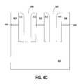
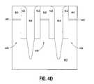
- a dielectric layer 410e.g., of silicon nitride, is formed overlying the structure of FIG. 4A in FIG. 4B , e.g., using a blanket deposition. Portions of dielectric layer 410 are then anisotropically removed, e.g., using a chemical wet etch or a plasma dry etch, so that remaining portions of dielectric layer 410 self align with and form spacers 412 on sidewalls of trenches 408 in FIG. 4C . For one embodiment, this is accomplished using an anisotropic etching process that selectively removes horizontal portions of dielectric layer 410 . Spacers 412 and remaining portions of hard mask layer 404 form a pattern for respectively exposing portions of substrate 400 for removal. The exposed portions of substrate 400 are removed in FIG. 4D so as to extend trenches 408 further into substrate 400 .
- Isolation regions 414such as shallow trench isolation (STI) regions, are then formed in FIG. 4D by filling the trenches with a suitable dielectric material, such as an oxide, e.g., a thermal oxide and/or a high-density-plasma (HDP) oxide, a spin-on dielectric material, e.g., hydrogen silsesquioxane (HSQ), hexamethyldisiloxane, octamethyltrisiloxane, etc.
- the dielectric materialis deposited in the trenches and overlying hard mask layer 404 and spacers 412 , such as by blanket deposition.
- Isolation regions 414define active regions 420 , where an isolation region 414 is located between successive active regions 420 , as shown in FIG. 4D .
- Each active regiondefines a site on which a future memory cell will be formed, as described below.
- Hard mask layer 404 , spacers 412 , and sacrificial layer 402are removed in FIG. 4E , such as by etching, e.g., using a wet or dry etch, exposing portions of substrate 400 corresponding to active regions 420 .
- Thisforms an elongated protuberance (or fin) 421 in each active region 420 , as shown in FIG. 4E .
- an isolation regionis located between successive fins 421 .
- FIG. 4Eshows the width W AR of the active regions to be greater than the width W IR of the isolation regions, for some embodiments, the width W IR of the isolation regions may be greater than or equal to the width W AR of the active regions (e.g., see FIG. 8B ).
- the ratio of the width W IR of the isolation regions to the width W AR of the active regions W IR /W ARis about 1.3:1.
- the exposed active regions 420(or portions of substrate 400 ), including fins 421 , are isotropically etched in FIG. 4F to decrease the height and width of the fins 421 of FIG. 4E and to form a rounded upper surface 423 on each fin 421 .
- the aspect ratio H Fin /W Fin(the ratio of the height H Fin of fins 421 to the width W Fin of the fins 421 ) is about 2:1 to about 10:1.
- fins 421protrude substantially from the centers of their respective active regions.
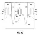
- a dielectric layer 422e.g., a tunnel oxide, is then formed on the exposed portions of substrate 400 , i.e., on active regions 420 , including fins 421 , in FIG. 4G .
- the dielectric layer 422 formed on each active region 420forms a tunnel dielectric layer of the memory cell to be formed on that active region 420 .
- Dielectric layer 422further defines a channel region 425 in each active region 420 on the sidewalls and upper surface of each of fins 421 .
- a floating gate 424is formed overlying the dielectric layer 422 formed on each active region 420 in FIG. 4G .
- floating gates 424are formed by forming a conductive layer, e.g., a layer of doped polysilicon, overlying the dielectric layer 422 formed on each active region 420 and isolation regions 414 in FIG. 4G , e.g., using a blanket deposition.
- portions of the conductive layer overlying isolation regions 414are removed from isolation regions 414 , e.g., using chemical mechanical polishing (CMP), so that an upper surface of each floating gate 424 is substantially flush with the upper surfaces of isolation regions 414 , as shown in FIG. 4G .
- CMPchemical mechanical polishing
- each of isolation regions 414is removed, such as by etching in an etch-back process, so that the upper surfaces of isolation regions 414 are recessed below the upper surfaces of floating gates 424 .
- the portions of floating gates 424 overlying the upper surfaces of the recessed isolation regions 414are isotropically etched to have elongated protrusions (or fins) 426 in FIG. 4I .
- fins 426are aligned with fins 421 , as shown in FIG. 4I .
- a dielectric layer 428is formed overlying isolation regions 414 and floating gates 424 in FIG. 4J , e.g., using a blanket deposition.
- dielectric layer 428may be one or more layers of dielectric material.
- dielectric layer 428could be of a multi-layer dielectric material commonly referred to as ONO (oxide-nitride-oxide).
- ONOoxide-nitride-oxide
- Other dielectric materialsmay be substituted for the ONO, such as tantalum oxide, barium strontium titanate, silicon nitride, and other materials providing dielectric properties.
- Dielectric layer 428forms an intergate dielectric layer of the memory cells overlying each active region 420 .
- a conductive layer 430is formed on dielectric layer 428 in FIG. 4J .
- Conductive layer 430forms a control gate layer (or word line) of the memory cells overlying each active region 420 , hereinafter memory cells 432 , e.g., floating-gate memory cells (or floating-gate transistors).
- Each memory cell 432includes a dielectric layer 422 , a floating gate 424 overlying the dielectric layer 422 , a portion of dielectric layer 428 overlying the floating gate 424 , and a portion of conductive layer 430 overlying the portion of dielectric layer 428 .
- Conductive layer 430is generally one or more layers of conductive material.
- conductive layer 430contains a conductively doped polysilicon.
- conductive layer 430includes a metal-containing layer overlying a polysilicon layer, e.g., a refractory metal silicide layer formed on a conductively doped polysilicon layer.
- the metals of chromium (Cr), cobalt (Co), hafnium (Hf), molybdenum (Mo), niobium (Nb), tantalum (Ta), titanium (Ti), tungsten (W), vanadium (V) and zirconium (Zr)are generally recognized as refractory metals.
- conductive layer 430contains multiple metal-containing layers, e.g., a titanium nitride (TiN) barrier layer on dielectric layer 428 , a titanium (Ti) adhesion layer on the barrier layer, and a tungsten (W) layer on the adhesion layer.
- TiNtitanium nitride
- Tititanium
- Wtungsten
- An insulative cap layer(not shown) is often formed overlying conductive layer 430 to protect and isolate conductive layer 430 from further processing.
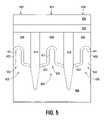
- a dielectric layer 528is formed overlying the structure of FIG. 4G , as shown in FIG. 5 . That is, dielectric layer 528 is formed overlying isolation regions 414 and floating gates 424 .
- dielectric layer 528is of a dielectric material having a relatively high dielectric constant (e.g., relative to an effective dielectric constant for an ONO layer), such as alumina (or aluminum oxide, Al 2 O 3 ) or other high-dielectric-constant material.
- Conductive layer 430is then formed on dielectric layer 528 in FIG. 5 to form memory cells 532 , e.g., floating-gate memory cells (or floating-gate transistors), that respectively overlie active regions 420 .
- Each memory cell 532includes a dielectric layer 422 , a floating gate 424 overlying the dielectric layer 422 , a portion of dielectric layer 528 overlying the floating gate 424 , and a portion of conductive layer 430 overlying the portion of dielectric layer 528 .
- dielectric layer 528forms an intergate dielectric layer of each of memory cells 532 and that conductive layer 430 forms a control gate layer of each of memory cells 532 .
- FIGS. 6A-6Fare cross-sectional views of a portion of a row of a memory array, such as a portion of a row of memory array 200 of FIG. 2 or a portion of a row of memory array 104 of FIG. 1 , during various stages of fabrication, according to an embodiment.
- FIG. 6Ais formed by removing a portion of each of isolation regions 414 of the structure of FIG. 4D , such as by etching in an etch-back process, so that upper surfaces of isolation regions 414 are recessed below hard mask layer 404 , sacrificial layer 402 and an upper surface of substrate 400 .
- Hard mask layer 404 , spacers 412 , and sacrificial layer 402are removed in FIG. 6B , exposing portions of substrate 400 corresponding to active regions 420 .
- the exposed active regions 420 (or portions of substrate 400 ), including fins 621are isotropically etched in FIG. 6C to decrease the height and width of the fins 621 of FIG. 6B and to form a rounded upper surface 623 on each fin 621 .
- fins 621protrude substantially from the centers of their respective active regions 420 .
- a dielectric layer 622e.g., a tunnel oxide, is then formed on the exposed portions of substrate 400 , i.e., on active regions 420 , including fins 621 , in FIG. 6D .
- the dielectric layer 622 formed on each active region 420forms a tunnel dielectric layer of the memory cell to be formed on that active region 420 .
- Dielectric layer 622further defines a channel region 625 in each active region 420 on the sidewalls and upper surface of each of fins 621 .
- a conductive layer 623e.g., a layer of doped polysilicon, is formed overlying dielectric layer 622 and isolation regions 414 in FIG. 6E , e.g., using a blanket deposition.
- portions of conductive layer 623are removed, such as by anisotropic etching, e.g., using a chemical wet etch or a plasma dry etch, exposing portions of dielectric layer 622 formed on each active region 420 and isolation regions 414 .
- the remaining portions of conductive layer 623respectively form floating gates 624 that respectively overlie active regions 420 .
- a floating gate 624overlies about half of a fin 621 of each active area 420 , as shown in FIG. 6F .
- each floating gate 624terminates at a location generally coinciding with an axis 627 that bisects a width, in the row direction, of a corresponding fin 621 , as shown in FIG. 6F .
- a dielectric layer 628e.g., similar to dielectric layer 428 discussed above in conjunction with FIG. 4J for one embodiment, is formed overlying floating gates 624 , the exposed portions of dielectric layer 622 formed on each active region 420 , and isolation regions 414 in FIG. 6F .
- a conductive layer 630e.g., similar to conductive layer 430 discussed above in conjunction with FIG. 4J for one embodiment, is then formed overlying dielectric layer 628 in FIG. 6F to form memory cells 632 , e.g., floating-gate memory cells (or floating-gate transistors), that respectively overlie active regions 420 .
- Each memory cell 632includes a dielectric layer 622 , a floating gate 624 overlying the dielectric layer 622 , a portion of dielectric layer 628 overlying the floating gate 624 , and a portion of conductive layer 630 overlying the portion of dielectric layer 628 .
- dielectric layer 628forms an intergate dielectric layer of each of memory cells 632 and that conductive layer 630 forms a control gate layer of each of memory cells 632 .
- each floating gate 624terminates at a location generally coinciding with an axis 627 a separation is formed between the axis 627 and an isolation region 414 , as shown in FIG. 6F .
- the separationshelp reduce floating-gate-to-floating-gate interference along the row (or the word line).
- portions of conductive layer 623 of FIG. 6Eare removed, such as by anisotropic etching, to form floating gates 724 that respectively overlie active regions 420 .
- a floating gate 724overlies more than half of a fin 621 of each active area 420 , as shown in FIG. 7 .
- each floating gate 724extends past the location that coincides with the axis 627 that bisects the width, in the row direction, of the corresponding fin 621 , as shown in FIG. 7 .
- Each floating gate 724forms a portion of a memory cell 732 that includes a dielectric layer 622 underlying that floating gate 724 , a portion of dielectric layer 628 overlying that floating gate 724 , and a portion of conductive layer 630 overlying the portion of dielectric layer 628 .
- dielectric layer 628forms an intergate dielectric layer of each of memory cells 732 and that conductive layer 630 forms a control gate layer of each of memory cells 732 .
- FIGS. 8A-8Eare cross-sectional views of a portion of a row of a memory array, such as a portion of a row of memory array 200 of FIG. 2 or a portion of a row of memory array 104 of FIG. 1 , during various stages of fabrication, according to an embodiment.
- FIG. 8Ais formed by removing one of the two sidewalls 412 from each trench 408 of the structure of FIG. 4C .
- the remaining spacers 412 and hard mask layer 404form a pattern for respectively exposing portions of substrate 400 for removal.
- the exposed portions substrate 400are removed in FIG. 8B so as to extend trenches 408 further into substrate 400 .
- Isolation regions 814e.g., similar to isolation regions 414 discussed above in conjunction with FIG.
- Isolation regions 814define active regions 820 , where an isolation region 814 is located between successive active regions 820 , as shown in FIG. 8B .
- Each active regiondefines a site on which a future memory cell will be formed, as described below.
- Hard mask layer 404 , spacers 412 , and sacrificial layer 402are removed in FIG. 8C , exposing portions of substrate 400 corresponding to active regions 820 .
- a sidewall of fin 821 in each of the active regions 820is adjacent and in contact with a sidewall of an isolation region 814 , as shown in FIG. 8C .
- a dielectric layer 822e.g., a tunnel oxide, is then formed on the exposed portions of substrate 400 , i.e., on active regions 820 , including a sidewall and an upper surface of each fin 821 , in FIG. 8D .
- the dielectric layer 822 formed on each active region 820forms a tunnel dielectric layer of the memory cell to be formed on that active region 820 .
- Dielectric layer 822further defines a channel region 825 in each active region 820 on a sidewall and upper surface of each of fins 821 . Note that when dielectric layer 822 is an oxide layer, the oxidation of the exposed portions of substrate 400 or fins 821 acts to round the corners of the exposed portions of substrate 400 or fins 821 , as shown in FIG. 8D .
- a floating gate 824is formed overlying the dielectric layer 822 formed on each active region 820 in FIG. 8E .
- floating gates 824are formed by forming a conductive layer, e.g., a layer of doped polysilicon, overlying the dielectric layer 822 formed on each active region 820 and isolation regions 814 in FIG. 8E , e.g., using a blanket deposition.
- portions of the conductive layer overlying isolation regions 814are removed from isolation regions 814 , e.g., using chemical mechanical polishing (CMP), so that an upper surface of each floating gate 824 is substantially flush with the upper surfaces of isolation regions 814 , as shown in FIG. 8E .
- CMPchemical mechanical polishing
- a dielectric layer 828e.g., similar to dielectric layer 428 discussed above in conjunction with FIG. 4J for one embodiment, is formed overlying isolation regions 814 and floating gates 824 in FIG. 8E , e.g., using a blanket deposition.
- a conductive layer 830e.g., similar to conductive layer 430 discussed above in conjunction with FIG. 4J for one embodiment, is then formed overlying dielectric layer 828 in FIG. 8E to form memory cells 832 , e.g., floating-gate memory cells (or floating-gate transistors), that respectively overlie active regions 420 .
- Each memory cell 832includes a dielectric layer 822 , a floating gate 824 overlying the dielectric layer 822 , a portion of dielectric layer 828 overlying the floating gate 824 , and a portion of conductive layer 830 overlying the portion of dielectric layer 828 .
- dielectric layer 828forms an intergate dielectric layer of each of memory cells 832 and that conductive layer 830 forms a control gate layer (or word line) of each of memory cells 832 .
- FIGS. 4A-4Jdepict a portion of a row of memory cells running parallel to a face plane of the drawings.
- the foregoing cross sectional viewscan depict a NOR- NAND-, NROM-, or AND-type memory device, with the differences occurring in the column direction in manners that are well understood in the art of memory fabrication.
- FIGS. 9A-9Care respectively cross-sectional views of portions of successive rows, e.g., respectively corresponding to successive word lines 202 of FIG. 2 , according to another embodiment. Note the cross-sections of FIGS. 9A-9C are formed as described above in conjunction with FIGS. 6A-6F and therefore FIGS. 9A-9C and FIGS. 6A-6F use common reference numbers.
- the floating gates 624 of every other roware formed on the same side, e.g., the same half or same side of the bisecting axis 627 , of their corresponding fins 621 .
- the floating gates 624 of an intervening rowi.e., a row between the every other rows having their floating gates on the same side of their fins 621
- the floating gates 624 of an intervening roware formed on a side (or side of the bisecting axis 627 ) of their corresponding fins 621 that is opposite to the side (or side of the bisecting axis 627 ) of the fins 621 on which the floating gates of the every other rows are formed.
- floating gates 624 i ⁇ 1 and 624 i+1are formed on the same side (or side of the bisecting axis 627 ) of their corresponding fins
- floating gates 624 i of row ilocated between row i ⁇ 1 and row i+1, are formed on a side (or side of the bisecting axis 627 ) of their corresponding fins 621 that is opposite to the side (or side of the bisecting axis 627 ) of the fins 621 on which floating gates 624 i ⁇ 1 and 624 i+1 respectively of row i ⁇ 1 and row i+1 are formed, as shown in FIGS. 9A-9C .
- the floating gates 624 of every other rowface in the same direction, whereas the floating gates 624 of an intervening row faces in a direction opposite to the floating gates of the every other rows. This configuration tends to reduce capacitive coupling of the floating gates in adjacent rows.
- FIGS. 10A-10Care respectively cross-sectional views of portions of successive rows, e.g., respectively corresponding to successive word lines 202 of FIG. 2 , according to another embodiment. Note the cross-sections of FIGS. 10A-10C are formed as described above in conjunction with FIGS. 6A-6E and 7 and therefore FIGS. 10A-10C and FIGS. 6A-6E and 7 use common reference numbers.
- the floating gates 724 of every other rowextend in the same direction past the location coinciding with the bisecting axis 627 of their corresponding fins 621 , whereas the floating gates 724 of an intervening row extend in a direction past the location coinciding with the bisecting axis 627 of their corresponding fins 621 that is opposite to that of the floating gates 724 of the every other rows. For example, as shown in FIGS.
- floating gates 724 i ⁇ 1 and 724 i+1respectively of row i ⁇ 1 and row i+1, extend in the same direction past the location coinciding with the bisecting axis 627 of their corresponding fins 621
- floating gates 724 i of row ilocated between row i ⁇ 1 and row i+1, extend in a direction past the location coinciding with the bisecting axis 627 of their corresponding fins 621 that is opposite to that of the floating gates 724 i ⁇ 1 and 724 i+1 respectively of row i ⁇ 1 and row i+1.
- the floating gates 724 of every other rowface in the same direction
- the floating gates 724 of an intervening rowfaces in a direction opposite to the floating gates of the every other rows.
Landscapes
- Non-Volatile Memory (AREA)
- Semiconductor Memories (AREA)
Abstract
Description
Claims (14)
Priority Applications (4)
| Application Number | Priority Date | Filing Date | Title |
|---|---|---|---|
| US11/514,004US7452766B2 (en) | 2006-08-31 | 2006-08-31 | Finned memory cells and the fabrication thereof |
| US12/257,100US7795664B2 (en) | 2006-08-31 | 2008-10-23 | Finned memory cells |
| US12/868,389US7968930B2 (en) | 2006-08-31 | 2010-08-25 | Finned memory cells |
| US13/117,364US8163610B2 (en) | 2006-08-31 | 2011-05-27 | Fabrication of finned memory arrays |
Applications Claiming Priority (1)
| Application Number | Priority Date | Filing Date | Title |
|---|---|---|---|
| US11/514,004US7452766B2 (en) | 2006-08-31 | 2006-08-31 | Finned memory cells and the fabrication thereof |
Related Child Applications (1)
| Application Number | Title | Priority Date | Filing Date |
|---|---|---|---|
| US12/257,100DivisionUS7795664B2 (en) | 2006-08-31 | 2008-10-23 | Finned memory cells |
Publications (2)
| Publication Number | Publication Date |
|---|---|
| US20080121970A1 US20080121970A1 (en) | 2008-05-29 |
| US7452766B2true US7452766B2 (en) | 2008-11-18 |
Family
ID=39462761
Family Applications (4)
| Application Number | Title | Priority Date | Filing Date |
|---|---|---|---|
| US11/514,004Active2026-09-06US7452766B2 (en) | 2006-08-31 | 2006-08-31 | Finned memory cells and the fabrication thereof |
| US12/257,100ActiveUS7795664B2 (en) | 2006-08-31 | 2008-10-23 | Finned memory cells |
| US12/868,389ActiveUS7968930B2 (en) | 2006-08-31 | 2010-08-25 | Finned memory cells |
| US13/117,364ActiveUS8163610B2 (en) | 2006-08-31 | 2011-05-27 | Fabrication of finned memory arrays |
Family Applications After (3)
| Application Number | Title | Priority Date | Filing Date |
|---|---|---|---|
| US12/257,100ActiveUS7795664B2 (en) | 2006-08-31 | 2008-10-23 | Finned memory cells |
| US12/868,389ActiveUS7968930B2 (en) | 2006-08-31 | 2010-08-25 | Finned memory cells |
| US13/117,364ActiveUS8163610B2 (en) | 2006-08-31 | 2011-05-27 | Fabrication of finned memory arrays |
Country Status (1)
| Country | Link |
|---|---|
| US (4) | US7452766B2 (en) |
Cited By (7)
| Publication number | Priority date | Publication date | Assignee | Title |
|---|---|---|---|---|
| US20090212340A1 (en)* | 2008-02-25 | 2009-08-27 | Samsung Electronics Co., Ltd. | Flash memory devices |
| US20090224357A1 (en)* | 2008-03-06 | 2009-09-10 | Micron Technology, Inc. | Devices with cavity-defined gates and methods of making the same |
| US20090273017A1 (en)* | 2008-04-30 | 2009-11-05 | Qimonda Flash Gmbh | Method for Forming Trenches on a Surface of a Semiconductor Substrate |
| CN102087972A (en)* | 2009-12-03 | 2011-06-08 | 英特尔公司 | Flash memory device having a curved upper surface |
| US8741722B2 (en) | 2011-05-31 | 2014-06-03 | International Business Machines Corporation | Formation of dividers between gate ends of field effect transistor devices |
| US9356121B2 (en) | 2012-02-27 | 2016-05-31 | International Business Machines Corporation | Divot-free planarization dielectric layer for replacement gate |
| US9847422B2 (en)* | 2003-05-28 | 2017-12-19 | Samsung Electronics Co., Ltd. | Semiconductor device and method of fabricating the same |
Families Citing this family (163)
| Publication number | Priority date | Publication date | Assignee | Title |
|---|---|---|---|---|
| JP4528718B2 (en)* | 2005-12-27 | 2010-08-18 | 株式会社東芝 | Method for manufacturing nonvolatile semiconductor memory |
| US20070166971A1 (en)* | 2006-01-17 | 2007-07-19 | Atmel Corporation | Manufacturing of silicon structures smaller than optical resolution limits |
| US20070166903A1 (en)* | 2006-01-17 | 2007-07-19 | Bohumil Lojek | Semiconductor structures formed by stepperless manufacturing |
| US8642441B1 (en)* | 2006-12-15 | 2014-02-04 | Spansion Llc | Self-aligned STI with single poly for manufacturing a flash memory device |
| US7824983B2 (en)* | 2008-06-02 | 2010-11-02 | Micron Technology, Inc. | Methods of providing electrical isolation in semiconductor structures |
| US7994020B2 (en)* | 2008-07-21 | 2011-08-09 | Advanced Micro Devices, Inc. | Method of forming finned semiconductor devices with trench isolation |
| KR20100081633A (en)* | 2009-01-06 | 2010-07-15 | 삼성전자주식회사 | Non-volatile memory device and manufacturing method used the same |
| US9059302B2 (en)* | 2009-04-06 | 2015-06-16 | Infineon Technologies Ag | Floating gate memory device with at least partially surrounding control gate |
| US8461640B2 (en) | 2009-09-08 | 2013-06-11 | Silicon Storage Technology, Inc. | FIN-FET non-volatile memory cell, and an array and method of manufacturing |
| CN103681847A (en)* | 2012-09-26 | 2014-03-26 | 中芯国际集成电路制造(上海)有限公司 | Semicircular window-shaped fin-type field-effect transistor and manufacturing method thereof |
| US8686492B2 (en)* | 2010-03-11 | 2014-04-01 | Spansion Llc | Non-volatile FINFET memory device and manufacturing method thereof |
| US9324576B2 (en) | 2010-05-27 | 2016-04-26 | Applied Materials, Inc. | Selective etch for silicon films |
| US8404560B2 (en) | 2010-10-12 | 2013-03-26 | International Business Machines Corporation | Devices with gate-to-gate isolation structures and methods of manufacture |
| US8455330B2 (en)* | 2010-10-12 | 2013-06-04 | International Business Machines Corporation | Devices with gate-to-gate isolation structures and methods of manufacture |
| US8298913B2 (en) | 2010-10-12 | 2012-10-30 | International Business Machines Corporation | Devices with gate-to-gate isolation structures and methods of manufacture |
| US10283321B2 (en) | 2011-01-18 | 2019-05-07 | Applied Materials, Inc. | Semiconductor processing system and methods using capacitively coupled plasma |
| EP2495762B1 (en)* | 2011-03-03 | 2017-11-01 | IMEC vzw | Method for producing a floating gate semiconductor memory device |
| US8999856B2 (en) | 2011-03-14 | 2015-04-07 | Applied Materials, Inc. | Methods for etch of sin films |
| US9064815B2 (en) | 2011-03-14 | 2015-06-23 | Applied Materials, Inc. | Methods for etch of metal and metal-oxide films |
| JP5646416B2 (en)* | 2011-09-01 | 2014-12-24 | 株式会社東芝 | Manufacturing method of semiconductor device |
| US8808563B2 (en) | 2011-10-07 | 2014-08-19 | Applied Materials, Inc. | Selective etch of silicon by way of metastable hydrogen termination |
| US8822284B2 (en) | 2012-02-09 | 2014-09-02 | United Microelectronics Corp. | Method for fabricating FinFETs and semiconductor structure fabricated using the method |
| US8883570B2 (en) | 2012-07-03 | 2014-11-11 | Taiwan Semiconductor Manufacturing Company, Ltd. | Multi-gate FETs and methods for forming the same |
| US9348385B2 (en)* | 2012-07-09 | 2016-05-24 | L. Pierre deRochement | Hybrid computing module |
| US9267739B2 (en) | 2012-07-18 | 2016-02-23 | Applied Materials, Inc. | Pedestal with multi-zone temperature control and multiple purge capabilities |
| US9373517B2 (en) | 2012-08-02 | 2016-06-21 | Applied Materials, Inc. | Semiconductor processing with DC assisted RF power for improved control |
| US9034770B2 (en) | 2012-09-17 | 2015-05-19 | Applied Materials, Inc. | Differential silicon oxide etch |
| US9023734B2 (en) | 2012-09-18 | 2015-05-05 | Applied Materials, Inc. | Radical-component oxide etch |
| US9390937B2 (en) | 2012-09-20 | 2016-07-12 | Applied Materials, Inc. | Silicon-carbon-nitride selective etch |
| US9132436B2 (en) | 2012-09-21 | 2015-09-15 | Applied Materials, Inc. | Chemical control features in wafer process equipment |
| US10721352B2 (en)* | 2012-10-17 | 2020-07-21 | Kedlin Company, LLC | Methods and systems for inbound and outbound call control |
| US9006079B2 (en)* | 2012-10-19 | 2015-04-14 | Taiwan Semiconductor Manufacturing Company, Ltd. | Methods for forming semiconductor fins with reduced widths |
| US8969212B2 (en) | 2012-11-20 | 2015-03-03 | Applied Materials, Inc. | Dry-etch selectivity |
| US8980763B2 (en) | 2012-11-30 | 2015-03-17 | Applied Materials, Inc. | Dry-etch for selective tungsten removal |
| US9111877B2 (en) | 2012-12-18 | 2015-08-18 | Applied Materials, Inc. | Non-local plasma oxide etch |
| US8921234B2 (en) | 2012-12-21 | 2014-12-30 | Applied Materials, Inc. | Selective titanium nitride etching |
| US10256079B2 (en) | 2013-02-08 | 2019-04-09 | Applied Materials, Inc. | Semiconductor processing systems having multiple plasma configurations |
| US9362130B2 (en) | 2013-03-01 | 2016-06-07 | Applied Materials, Inc. | Enhanced etching processes using remote plasma sources |
| US9040422B2 (en) | 2013-03-05 | 2015-05-26 | Applied Materials, Inc. | Selective titanium nitride removal |
| US20140271097A1 (en) | 2013-03-15 | 2014-09-18 | Applied Materials, Inc. | Processing systems and methods for halide scavenging |
| US20140315371A1 (en)* | 2013-04-17 | 2014-10-23 | International Business Machines Corporation | Methods of forming isolation regions for bulk finfet semiconductor devices |
| US9493879B2 (en) | 2013-07-12 | 2016-11-15 | Applied Materials, Inc. | Selective sputtering for pattern transfer |
| KR102073967B1 (en) | 2013-07-30 | 2020-03-02 | 삼성전자주식회사 | Semiconductor device including field effect transistor |
| US9773648B2 (en) | 2013-08-30 | 2017-09-26 | Applied Materials, Inc. | Dual discharge modes operation for remote plasma |
| US9437497B2 (en) | 2013-10-18 | 2016-09-06 | Taiwan Semiconductor Manufacturing Company, Ltd. | Method of making a FinFET device |
| US9576809B2 (en) | 2013-11-04 | 2017-02-21 | Applied Materials, Inc. | Etch suppression with germanium |
| US9520303B2 (en) | 2013-11-12 | 2016-12-13 | Applied Materials, Inc. | Aluminum selective etch |
| US9245762B2 (en) | 2013-12-02 | 2016-01-26 | Applied Materials, Inc. | Procedure for etch rate consistency |
| US9287095B2 (en) | 2013-12-17 | 2016-03-15 | Applied Materials, Inc. | Semiconductor system assemblies and methods of operation |
| US9287134B2 (en) | 2014-01-17 | 2016-03-15 | Applied Materials, Inc. | Titanium oxide etch |
| US9853154B2 (en)* | 2014-01-24 | 2017-12-26 | Taiwan Semiconductor Manufacturing Company Ltd. | Embedded source or drain region of transistor with downward tapered region under facet region |
| US9293568B2 (en) | 2014-01-27 | 2016-03-22 | Applied Materials, Inc. | Method of fin patterning |
| US9396989B2 (en) | 2014-01-27 | 2016-07-19 | Applied Materials, Inc. | Air gaps between copper lines |
| US9385028B2 (en) | 2014-02-03 | 2016-07-05 | Applied Materials, Inc. | Air gap process |
| US9499898B2 (en) | 2014-03-03 | 2016-11-22 | Applied Materials, Inc. | Layered thin film heater and method of fabrication |
| US9299575B2 (en) | 2014-03-17 | 2016-03-29 | Applied Materials, Inc. | Gas-phase tungsten etch |
| US9299537B2 (en) | 2014-03-20 | 2016-03-29 | Applied Materials, Inc. | Radial waveguide systems and methods for post-match control of microwaves |
| US9903020B2 (en) | 2014-03-31 | 2018-02-27 | Applied Materials, Inc. | Generation of compact alumina passivation layers on aluminum plasma equipment components |
| US9269590B2 (en) | 2014-04-07 | 2016-02-23 | Applied Materials, Inc. | Spacer formation |
| US9309598B2 (en) | 2014-05-28 | 2016-04-12 | Applied Materials, Inc. | Oxide and metal removal |
| US9460956B2 (en)* | 2014-06-12 | 2016-10-04 | Taiwan Semiconductor Manufacturing Company Limited | Method of forming shallow trench isolation and semiconductor device |
| US9406523B2 (en) | 2014-06-19 | 2016-08-02 | Applied Materials, Inc. | Highly selective doped oxide removal method |
| US9378969B2 (en) | 2014-06-19 | 2016-06-28 | Applied Materials, Inc. | Low temperature gas-phase carbon removal |
| US9425058B2 (en) | 2014-07-24 | 2016-08-23 | Applied Materials, Inc. | Simplified litho-etch-litho-etch process |
| US9496167B2 (en) | 2014-07-31 | 2016-11-15 | Applied Materials, Inc. | Integrated bit-line airgap formation and gate stack post clean |
| US9378978B2 (en)* | 2014-07-31 | 2016-06-28 | Applied Materials, Inc. | Integrated oxide recess and floating gate fin trimming |
| US9659753B2 (en) | 2014-08-07 | 2017-05-23 | Applied Materials, Inc. | Grooved insulator to reduce leakage current |
| US9553102B2 (en) | 2014-08-19 | 2017-01-24 | Applied Materials, Inc. | Tungsten separation |
| US10504893B2 (en)* | 2014-08-29 | 2019-12-10 | Taiwan Semiconductor Manufacturing Co., Ltd. | Fin field effect transistor (FinFET) device with protection layer |
| US9355856B2 (en) | 2014-09-12 | 2016-05-31 | Applied Materials, Inc. | V trench dry etch |
| US9355862B2 (en) | 2014-09-24 | 2016-05-31 | Applied Materials, Inc. | Fluorine-based hardmask removal |
| US9368364B2 (en) | 2014-09-24 | 2016-06-14 | Applied Materials, Inc. | Silicon etch process with tunable selectivity to SiO2 and other materials |
| US9613822B2 (en) | 2014-09-25 | 2017-04-04 | Applied Materials, Inc. | Oxide etch selectivity enhancement |
| US9966240B2 (en) | 2014-10-14 | 2018-05-08 | Applied Materials, Inc. | Systems and methods for internal surface conditioning assessment in plasma processing equipment |
| US9355922B2 (en) | 2014-10-14 | 2016-05-31 | Applied Materials, Inc. | Systems and methods for internal surface conditioning in plasma processing equipment |
| US11637002B2 (en) | 2014-11-26 | 2023-04-25 | Applied Materials, Inc. | Methods and systems to enhance process uniformity |
| US9299583B1 (en) | 2014-12-05 | 2016-03-29 | Applied Materials, Inc. | Aluminum oxide selective etch |
| US10224210B2 (en) | 2014-12-09 | 2019-03-05 | Applied Materials, Inc. | Plasma processing system with direct outlet toroidal plasma source |
| US10573496B2 (en) | 2014-12-09 | 2020-02-25 | Applied Materials, Inc. | Direct outlet toroidal plasma source |
| US9793379B2 (en) | 2014-12-12 | 2017-10-17 | International Business Machines Corporation | FinFET spacer without substrate gouging or spacer foot |
| US9502258B2 (en) | 2014-12-23 | 2016-11-22 | Applied Materials, Inc. | Anisotropic gap etch |
| US9343272B1 (en) | 2015-01-08 | 2016-05-17 | Applied Materials, Inc. | Self-aligned process |
| US11257693B2 (en) | 2015-01-09 | 2022-02-22 | Applied Materials, Inc. | Methods and systems to improve pedestal temperature control |
| US9373522B1 (en) | 2015-01-22 | 2016-06-21 | Applied Mateials, Inc. | Titanium nitride removal |
| US9859275B2 (en) | 2015-01-26 | 2018-01-02 | International Business Machines Corporation | Silicon nitride fill for PC gap regions to increase cell density |
| US9449846B2 (en) | 2015-01-28 | 2016-09-20 | Applied Materials, Inc. | Vertical gate separation |
| US9728437B2 (en) | 2015-02-03 | 2017-08-08 | Applied Materials, Inc. | High temperature chuck for plasma processing systems |
| US20160225652A1 (en) | 2015-02-03 | 2016-08-04 | Applied Materials, Inc. | Low temperature chuck for plasma processing systems |
| US9881805B2 (en) | 2015-03-02 | 2018-01-30 | Applied Materials, Inc. | Silicon selective removal |
| KR20160143942A (en) | 2015-06-04 | 2016-12-15 | 삼성전자주식회사 | Method of manufacturing semiconductor device |
| US9691645B2 (en) | 2015-08-06 | 2017-06-27 | Applied Materials, Inc. | Bolted wafer chuck thermal management systems and methods for wafer processing systems |
| US9741593B2 (en) | 2015-08-06 | 2017-08-22 | Applied Materials, Inc. | Thermal management systems and methods for wafer processing systems |
| US9349605B1 (en) | 2015-08-07 | 2016-05-24 | Applied Materials, Inc. | Oxide etch selectivity systems and methods |
| US10504700B2 (en) | 2015-08-27 | 2019-12-10 | Applied Materials, Inc. | Plasma etching systems and methods with secondary plasma injection |
| US10504754B2 (en) | 2016-05-19 | 2019-12-10 | Applied Materials, Inc. | Systems and methods for improved semiconductor etching and component protection |
| US10522371B2 (en) | 2016-05-19 | 2019-12-31 | Applied Materials, Inc. | Systems and methods for improved semiconductor etching and component protection |
| US10276726B2 (en)* | 2016-05-31 | 2019-04-30 | Taiwan Semiconductor Manufacturing Co., Ltd. | Non-volatile memory cell and non-volatile memory |
| US9865484B1 (en) | 2016-06-29 | 2018-01-09 | Applied Materials, Inc. | Selective etch using material modification and RF pulsing |
| JP6688698B2 (en)* | 2016-07-08 | 2020-04-28 | ルネサスエレクトロニクス株式会社 | Semiconductor device and manufacturing method thereof |
| US10062575B2 (en) | 2016-09-09 | 2018-08-28 | Applied Materials, Inc. | Poly directional etch by oxidation |
| US10629473B2 (en) | 2016-09-09 | 2020-04-21 | Applied Materials, Inc. | Footing removal for nitride spacer |
| US10546729B2 (en) | 2016-10-04 | 2020-01-28 | Applied Materials, Inc. | Dual-channel showerhead with improved profile |
| US10062585B2 (en) | 2016-10-04 | 2018-08-28 | Applied Materials, Inc. | Oxygen compatible plasma source |
| US9721789B1 (en) | 2016-10-04 | 2017-08-01 | Applied Materials, Inc. | Saving ion-damaged spacers |
| US9934942B1 (en) | 2016-10-04 | 2018-04-03 | Applied Materials, Inc. | Chamber with flow-through source |
| US10062579B2 (en) | 2016-10-07 | 2018-08-28 | Applied Materials, Inc. | Selective SiN lateral recess |
| US9947549B1 (en) | 2016-10-10 | 2018-04-17 | Applied Materials, Inc. | Cobalt-containing material removal |
| US10163696B2 (en) | 2016-11-11 | 2018-12-25 | Applied Materials, Inc. | Selective cobalt removal for bottom up gapfill |
| US9768034B1 (en) | 2016-11-11 | 2017-09-19 | Applied Materials, Inc. | Removal methods for high aspect ratio structures |
| US10026621B2 (en) | 2016-11-14 | 2018-07-17 | Applied Materials, Inc. | SiN spacer profile patterning |
| US10242908B2 (en) | 2016-11-14 | 2019-03-26 | Applied Materials, Inc. | Airgap formation with damage-free copper |
| US10566206B2 (en) | 2016-12-27 | 2020-02-18 | Applied Materials, Inc. | Systems and methods for anisotropic material breakthrough |
| US10403507B2 (en) | 2017-02-03 | 2019-09-03 | Applied Materials, Inc. | Shaped etch profile with oxidation |
| US10431429B2 (en) | 2017-02-03 | 2019-10-01 | Applied Materials, Inc. | Systems and methods for radial and azimuthal control of plasma uniformity |
| US10043684B1 (en) | 2017-02-06 | 2018-08-07 | Applied Materials, Inc. | Self-limiting atomic thermal etching systems and methods |
| US10319739B2 (en) | 2017-02-08 | 2019-06-11 | Applied Materials, Inc. | Accommodating imperfectly aligned memory holes |
| US10943834B2 (en) | 2017-03-13 | 2021-03-09 | Applied Materials, Inc. | Replacement contact process |
| US10319649B2 (en) | 2017-04-11 | 2019-06-11 | Applied Materials, Inc. | Optical emission spectroscopy (OES) for remote plasma monitoring |
| US9954082B1 (en) | 2017-04-25 | 2018-04-24 | United Microelectronics Corp. | Method of fabricating an embedded nonvolatile memory device |
| JP7176860B6 (en) | 2017-05-17 | 2022-12-16 | アプライド マテリアルズ インコーポレイテッド | Semiconductor processing chamber to improve precursor flow |
| US11276559B2 (en) | 2017-05-17 | 2022-03-15 | Applied Materials, Inc. | Semiconductor processing chamber for multiple precursor flow |
| US11276590B2 (en) | 2017-05-17 | 2022-03-15 | Applied Materials, Inc. | Multi-zone semiconductor substrate supports |
| US10049891B1 (en) | 2017-05-31 | 2018-08-14 | Applied Materials, Inc. | Selective in situ cobalt residue removal |
| US10497579B2 (en) | 2017-05-31 | 2019-12-03 | Applied Materials, Inc. | Water-free etching methods |
| US10920320B2 (en) | 2017-06-16 | 2021-02-16 | Applied Materials, Inc. | Plasma health determination in semiconductor substrate processing reactors |
| US10541246B2 (en) | 2017-06-26 | 2020-01-21 | Applied Materials, Inc. | 3D flash memory cells which discourage cross-cell electrical tunneling |
| US10727080B2 (en) | 2017-07-07 | 2020-07-28 | Applied Materials, Inc. | Tantalum-containing material removal |
| US10541184B2 (en) | 2017-07-11 | 2020-01-21 | Applied Materials, Inc. | Optical emission spectroscopic techniques for monitoring etching |
| US10354889B2 (en) | 2017-07-17 | 2019-07-16 | Applied Materials, Inc. | Non-halogen etching of silicon-containing materials |
| US10043674B1 (en) | 2017-08-04 | 2018-08-07 | Applied Materials, Inc. | Germanium etching systems and methods |
| US10170336B1 (en) | 2017-08-04 | 2019-01-01 | Applied Materials, Inc. | Methods for anisotropic control of selective silicon removal |
| US10297458B2 (en) | 2017-08-07 | 2019-05-21 | Applied Materials, Inc. | Process window widening using coated parts in plasma etch processes |
| US10128086B1 (en) | 2017-10-24 | 2018-11-13 | Applied Materials, Inc. | Silicon pretreatment for nitride removal |
| US10283324B1 (en) | 2017-10-24 | 2019-05-07 | Applied Materials, Inc. | Oxygen treatment for nitride etching |
| US10256112B1 (en) | 2017-12-08 | 2019-04-09 | Applied Materials, Inc. | Selective tungsten removal |
| US10903054B2 (en) | 2017-12-19 | 2021-01-26 | Applied Materials, Inc. | Multi-zone gas distribution systems and methods |
| US11328909B2 (en) | 2017-12-22 | 2022-05-10 | Applied Materials, Inc. | Chamber conditioning and removal processes |
| US10854426B2 (en) | 2018-01-08 | 2020-12-01 | Applied Materials, Inc. | Metal recess for semiconductor structures |
| US10964512B2 (en) | 2018-02-15 | 2021-03-30 | Applied Materials, Inc. | Semiconductor processing chamber multistage mixing apparatus and methods |
| US10679870B2 (en) | 2018-02-15 | 2020-06-09 | Applied Materials, Inc. | Semiconductor processing chamber multistage mixing apparatus |
| TWI766433B (en) | 2018-02-28 | 2022-06-01 | 美商應用材料股份有限公司 | Systems and methods to form airgaps |
| US10593560B2 (en) | 2018-03-01 | 2020-03-17 | Applied Materials, Inc. | Magnetic induction plasma source for semiconductor processes and equipment |
| US10319600B1 (en) | 2018-03-12 | 2019-06-11 | Applied Materials, Inc. | Thermal silicon etch |
| US10497573B2 (en) | 2018-03-13 | 2019-12-03 | Applied Materials, Inc. | Selective atomic layer etching of semiconductor materials |
| US10573527B2 (en) | 2018-04-06 | 2020-02-25 | Applied Materials, Inc. | Gas-phase selective etching systems and methods |
| US10490406B2 (en) | 2018-04-10 | 2019-11-26 | Appled Materials, Inc. | Systems and methods for material breakthrough |
| US10699879B2 (en) | 2018-04-17 | 2020-06-30 | Applied Materials, Inc. | Two piece electrode assembly with gap for plasma control |
| US10886137B2 (en) | 2018-04-30 | 2021-01-05 | Applied Materials, Inc. | Selective nitride removal |
| US10872778B2 (en) | 2018-07-06 | 2020-12-22 | Applied Materials, Inc. | Systems and methods utilizing solid-phase etchants |
| US10755941B2 (en) | 2018-07-06 | 2020-08-25 | Applied Materials, Inc. | Self-limiting selective etching systems and methods |
| US10672642B2 (en) | 2018-07-24 | 2020-06-02 | Applied Materials, Inc. | Systems and methods for pedestal configuration |
| US11049755B2 (en) | 2018-09-14 | 2021-06-29 | Applied Materials, Inc. | Semiconductor substrate supports with embedded RF shield |
| US10892198B2 (en) | 2018-09-14 | 2021-01-12 | Applied Materials, Inc. | Systems and methods for improved performance in semiconductor processing |
| US11062887B2 (en) | 2018-09-17 | 2021-07-13 | Applied Materials, Inc. | High temperature RF heater pedestals |
| US11417534B2 (en) | 2018-09-21 | 2022-08-16 | Applied Materials, Inc. | Selective material removal |
| US11682560B2 (en) | 2018-10-11 | 2023-06-20 | Applied Materials, Inc. | Systems and methods for hafnium-containing film removal |
| US11121002B2 (en) | 2018-10-24 | 2021-09-14 | Applied Materials, Inc. | Systems and methods for etching metals and metal derivatives |
| US11437242B2 (en) | 2018-11-27 | 2022-09-06 | Applied Materials, Inc. | Selective removal of silicon-containing materials |
| US11721527B2 (en) | 2019-01-07 | 2023-08-08 | Applied Materials, Inc. | Processing chamber mixing systems |
| US10920319B2 (en) | 2019-01-11 | 2021-02-16 | Applied Materials, Inc. | Ceramic showerheads with conductive electrodes |
| US11455257B2 (en)* | 2019-04-07 | 2022-09-27 | Intel Corporation | Ultra-secure accelerators |
| CN114334986A (en)* | 2021-12-15 | 2022-04-12 | 华虹半导体(无锡)有限公司 | Semiconductor structure and forming method thereof |
| US20230197826A1 (en)* | 2021-12-21 | 2023-06-22 | Christine RADLINGER | Self-aligned gate endcap (sage) architectures with improved cap |
Citations (3)
| Publication number | Priority date | Publication date | Assignee | Title |
|---|---|---|---|---|
| US7026195B2 (en) | 2004-05-21 | 2006-04-11 | Taiwan Semiconductor Manufacturing Co., Ltd. | Planarizing method for forming FIN-FET device |
| US20060141706A1 (en) | 2004-12-28 | 2006-06-29 | Seung-Wan Hong | Methods of forming non-volatile semiconductor memory devices using prominences and trenches, and devices so formed |
| US7297600B2 (en)* | 2004-06-04 | 2007-11-20 | Samsung Electronics Co., Ltd. | Methods of forming fin field effect transistors using oxidation barrier layers |
Family Cites Families (3)
| Publication number | Priority date | Publication date | Assignee | Title |
|---|---|---|---|---|
| KR100621628B1 (en)* | 2004-05-31 | 2006-09-19 | 삼성전자주식회사 | Nonvolatile Memory Cells and Their Formation Methods |
| KR100663366B1 (en)* | 2005-10-26 | 2007-01-02 | 삼성전자주식회사 | Flash memory device manufacturing method having self-aligned floating gate and related devices |
| US7790516B2 (en)* | 2006-07-10 | 2010-09-07 | Qimonda Ag | Method of manufacturing at least one semiconductor component and memory cells |
- 2006
- 2006-08-31USUS11/514,004patent/US7452766B2/enactiveActive
- 2008
- 2008-10-23USUS12/257,100patent/US7795664B2/enactiveActive
- 2010
- 2010-08-25USUS12/868,389patent/US7968930B2/enactiveActive
- 2011
- 2011-05-27USUS13/117,364patent/US8163610B2/enactiveActive
Patent Citations (3)
| Publication number | Priority date | Publication date | Assignee | Title |
|---|---|---|---|---|
| US7026195B2 (en) | 2004-05-21 | 2006-04-11 | Taiwan Semiconductor Manufacturing Co., Ltd. | Planarizing method for forming FIN-FET device |
| US7297600B2 (en)* | 2004-06-04 | 2007-11-20 | Samsung Electronics Co., Ltd. | Methods of forming fin field effect transistors using oxidation barrier layers |
| US20060141706A1 (en) | 2004-12-28 | 2006-06-29 | Seung-Wan Hong | Methods of forming non-volatile semiconductor memory devices using prominences and trenches, and devices so formed |
Cited By (11)
| Publication number | Priority date | Publication date | Assignee | Title |
|---|---|---|---|---|
| US9847422B2 (en)* | 2003-05-28 | 2017-12-19 | Samsung Electronics Co., Ltd. | Semiconductor device and method of fabricating the same |
| US20090212340A1 (en)* | 2008-02-25 | 2009-08-27 | Samsung Electronics Co., Ltd. | Flash memory devices |
| US20090224357A1 (en)* | 2008-03-06 | 2009-09-10 | Micron Technology, Inc. | Devices with cavity-defined gates and methods of making the same |
| US7915659B2 (en)* | 2008-03-06 | 2011-03-29 | Micron Technology, Inc. | Devices with cavity-defined gates and methods of making the same |
| US20090273017A1 (en)* | 2008-04-30 | 2009-11-05 | Qimonda Flash Gmbh | Method for Forming Trenches on a Surface of a Semiconductor Substrate |
| US7785953B2 (en)* | 2008-04-30 | 2010-08-31 | Qimonda Ag | Method for forming trenches on a surface of a semiconductor substrate |
| CN102087972A (en)* | 2009-12-03 | 2011-06-08 | 英特尔公司 | Flash memory device having a curved upper surface |
| CN102087972B (en)* | 2009-12-03 | 2014-04-30 | 英特尔公司 | Flash memory device having a curved upper surface |
| US8741722B2 (en) | 2011-05-31 | 2014-06-03 | International Business Machines Corporation | Formation of dividers between gate ends of field effect transistor devices |
| US9356121B2 (en) | 2012-02-27 | 2016-05-31 | International Business Machines Corporation | Divot-free planarization dielectric layer for replacement gate |
| US9876091B2 (en) | 2012-02-27 | 2018-01-23 | International Business Machines Corporation | Divot-free planarization dielectric layer for replacement gate |
Also Published As
| Publication number | Publication date |
|---|---|
| US20090045449A1 (en) | 2009-02-19 |
| US7968930B2 (en) | 2011-06-28 |
| US7795664B2 (en) | 2010-09-14 |
| US20100320523A1 (en) | 2010-12-23 |
| US8163610B2 (en) | 2012-04-24 |
| US20080121970A1 (en) | 2008-05-29 |
| US20110230033A1 (en) | 2011-09-22 |
Similar Documents
| Publication | Publication Date | Title |
|---|---|---|
| US7452766B2 (en) | Finned memory cells and the fabrication thereof | |
| US7811935B2 (en) | Isolation regions and their formation | |
| US7453134B2 (en) | Integrated circuit device with a circuit element formed on an active region having rounded corners | |
| JP4644258B2 (en) | Method for forming a non-volatile memory array | |
| KR101456811B1 (en) | Memory arrays having different substantially vertical distances between adjacent memory cells | |
| US7968425B2 (en) | Isolation regions | |
| US20070195571A1 (en) | Bit line coupling | |
| US20060267070A1 (en) | Gate coupling in floating-gate memory cells | |
| US7485529B2 (en) | Method of fabricating non-volatile memory | |
| US8693231B2 (en) | Couplings within memory devices | |
| US6939764B2 (en) | Methods of forming memory cells having self-aligned silicide | |
| US8193590B2 (en) | Interconnecting bit lines in memory devices for multiplexing | |
| US7348236B2 (en) | Formation of memory cells and select gates of NAND memory arrays | |
| US20060043368A1 (en) | Flash cell structures and methods of formation |
Legal Events
| Date | Code | Title | Description |
|---|---|---|---|
| AS | Assignment | Owner name:MICRON TECHNOLOGY, INC., IDAHO Free format text:ASSIGNMENT OF ASSIGNORS INTEREST;ASSIGNOR:ARITOME, SEIICHI;REEL/FRAME:018255/0834 Effective date:20060829 | |
| FEPP | Fee payment procedure | Free format text:PAYOR NUMBER ASSIGNED (ORIGINAL EVENT CODE: ASPN); ENTITY STATUS OF PATENT OWNER: LARGE ENTITY | |
| STCF | Information on status: patent grant | Free format text:PATENTED CASE | |
| FPAY | Fee payment | Year of fee payment:4 | |
| FPAY | Fee payment | Year of fee payment:8 | |
| AS | Assignment | Owner name:U.S. BANK NATIONAL ASSOCIATION, AS COLLATERAL AGENT, CALIFORNIA Free format text:SECURITY INTEREST;ASSIGNOR:MICRON TECHNOLOGY, INC.;REEL/FRAME:038669/0001 Effective date:20160426 Owner name:U.S. BANK NATIONAL ASSOCIATION, AS COLLATERAL AGEN Free format text:SECURITY INTEREST;ASSIGNOR:MICRON TECHNOLOGY, INC.;REEL/FRAME:038669/0001 Effective date:20160426 | |
| AS | Assignment | Owner name:MORGAN STANLEY SENIOR FUNDING, INC., AS COLLATERAL AGENT, MARYLAND Free format text:PATENT SECURITY AGREEMENT;ASSIGNOR:MICRON TECHNOLOGY, INC.;REEL/FRAME:038954/0001 Effective date:20160426 Owner name:MORGAN STANLEY SENIOR FUNDING, INC., AS COLLATERAL Free format text:PATENT SECURITY AGREEMENT;ASSIGNOR:MICRON TECHNOLOGY, INC.;REEL/FRAME:038954/0001 Effective date:20160426 | |
| AS | Assignment | Owner name:U.S. BANK NATIONAL ASSOCIATION, AS COLLATERAL AGENT, CALIFORNIA Free format text:CORRECTIVE ASSIGNMENT TO CORRECT THE REPLACE ERRONEOUSLY FILED PATENT #7358718 WITH THE CORRECT PATENT #7358178 PREVIOUSLY RECORDED ON REEL 038669 FRAME 0001. ASSIGNOR(S) HEREBY CONFIRMS THE SECURITY INTEREST;ASSIGNOR:MICRON TECHNOLOGY, INC.;REEL/FRAME:043079/0001 Effective date:20160426 Owner name:U.S. BANK NATIONAL ASSOCIATION, AS COLLATERAL AGEN Free format text:CORRECTIVE ASSIGNMENT TO CORRECT THE REPLACE ERRONEOUSLY FILED PATENT #7358718 WITH THE CORRECT PATENT #7358178 PREVIOUSLY RECORDED ON REEL 038669 FRAME 0001. ASSIGNOR(S) HEREBY CONFIRMS THE SECURITY INTEREST;ASSIGNOR:MICRON TECHNOLOGY, INC.;REEL/FRAME:043079/0001 Effective date:20160426 | |
| AS | Assignment | Owner name:JPMORGAN CHASE BANK, N.A., AS COLLATERAL AGENT, ILLINOIS Free format text:SECURITY INTEREST;ASSIGNORS:MICRON TECHNOLOGY, INC.;MICRON SEMICONDUCTOR PRODUCTS, INC.;REEL/FRAME:047540/0001 Effective date:20180703 Owner name:JPMORGAN CHASE BANK, N.A., AS COLLATERAL AGENT, IL Free format text:SECURITY INTEREST;ASSIGNORS:MICRON TECHNOLOGY, INC.;MICRON SEMICONDUCTOR PRODUCTS, INC.;REEL/FRAME:047540/0001 Effective date:20180703 | |
| AS | Assignment | Owner name:MICRON TECHNOLOGY, INC., IDAHO Free format text:RELEASE BY SECURED PARTY;ASSIGNOR:U.S. BANK NATIONAL ASSOCIATION, AS COLLATERAL AGENT;REEL/FRAME:047243/0001 Effective date:20180629 | |
| AS | Assignment | Owner name:MICRON TECHNOLOGY, INC., IDAHO Free format text:RELEASE BY SECURED PARTY;ASSIGNOR:MORGAN STANLEY SENIOR FUNDING, INC., AS COLLATERAL AGENT;REEL/FRAME:050937/0001 Effective date:20190731 | |
| AS | Assignment | Owner name:MICRON TECHNOLOGY, INC., IDAHO Free format text:RELEASE BY SECURED PARTY;ASSIGNOR:JPMORGAN CHASE BANK, N.A., AS COLLATERAL AGENT;REEL/FRAME:051028/0001 Effective date:20190731 Owner name:MICRON SEMICONDUCTOR PRODUCTS, INC., IDAHO Free format text:RELEASE BY SECURED PARTY;ASSIGNOR:JPMORGAN CHASE BANK, N.A., AS COLLATERAL AGENT;REEL/FRAME:051028/0001 Effective date:20190731 | |
| MAFP | Maintenance fee payment | Free format text:PAYMENT OF MAINTENANCE FEE, 12TH YEAR, LARGE ENTITY (ORIGINAL EVENT CODE: M1553); ENTITY STATUS OF PATENT OWNER: LARGE ENTITY Year of fee payment:12 |