US7452574B2 - Method to reduce adhesion between a polymerizable layer and a substrate employing a fluorine-containing layer - Google Patents
Method to reduce adhesion between a polymerizable layer and a substrate employing a fluorine-containing layerDownload PDFInfo
- Publication number
- US7452574B2 US7452574B2US10/375,817US37581703AUS7452574B2US 7452574 B2US7452574 B2US 7452574B2US 37581703 AUS37581703 AUS 37581703AUS 7452574 B2US7452574 B2US 7452574B2
- Authority
- US
- United States
- Prior art keywords
- layer
- recited
- molecule
- functional
- perfluoro
- Prior art date
- Legal status (The legal status is an assumption and is not a legal conclusion. Google has not performed a legal analysis and makes no representation as to the accuracy of the status listed.)
- Expired - Lifetime, expires
Links
Images


Classifications
- B—PERFORMING OPERATIONS; TRANSPORTING
- B82—NANOTECHNOLOGY
- B82Y—SPECIFIC USES OR APPLICATIONS OF NANOSTRUCTURES; MEASUREMENT OR ANALYSIS OF NANOSTRUCTURES; MANUFACTURE OR TREATMENT OF NANOSTRUCTURES
- B82Y10/00—Nanotechnology for information processing, storage or transmission, e.g. quantum computing or single electron logic
- B—PERFORMING OPERATIONS; TRANSPORTING
- B81—MICROSTRUCTURAL TECHNOLOGY
- B81C—PROCESSES OR APPARATUS SPECIALLY ADAPTED FOR THE MANUFACTURE OR TREATMENT OF MICROSTRUCTURAL DEVICES OR SYSTEMS
- B81C99/00—Subject matter not provided for in other groups of this subclass
- B81C99/0075—Manufacture of substrate-free structures
- B81C99/008—Manufacture of substrate-free structures separating the processed structure from a mother substrate
- B—PERFORMING OPERATIONS; TRANSPORTING
- B82—NANOTECHNOLOGY
- B82Y—SPECIFIC USES OR APPLICATIONS OF NANOSTRUCTURES; MEASUREMENT OR ANALYSIS OF NANOSTRUCTURES; MANUFACTURE OR TREATMENT OF NANOSTRUCTURES
- B82Y40/00—Manufacture or treatment of nanostructures
- G—PHYSICS
- G03—PHOTOGRAPHY; CINEMATOGRAPHY; ANALOGOUS TECHNIQUES USING WAVES OTHER THAN OPTICAL WAVES; ELECTROGRAPHY; HOLOGRAPHY
- G03F—PHOTOMECHANICAL PRODUCTION OF TEXTURED OR PATTERNED SURFACES, e.g. FOR PRINTING, FOR PROCESSING OF SEMICONDUCTOR DEVICES; MATERIALS THEREFOR; ORIGINALS THEREFOR; APPARATUS SPECIALLY ADAPTED THEREFOR
- G03F7/00—Photomechanical, e.g. photolithographic, production of textured or patterned surfaces, e.g. printing surfaces; Materials therefor, e.g. comprising photoresists; Apparatus specially adapted therefor
- G03F7/0002—Lithographic processes using patterning methods other than those involving the exposure to radiation, e.g. by stamping
- G—PHYSICS
- G03—PHOTOGRAPHY; CINEMATOGRAPHY; ANALOGOUS TECHNIQUES USING WAVES OTHER THAN OPTICAL WAVES; ELECTROGRAPHY; HOLOGRAPHY
- G03F—PHOTOMECHANICAL PRODUCTION OF TEXTURED OR PATTERNED SURFACES, e.g. FOR PRINTING, FOR PROCESSING OF SEMICONDUCTOR DEVICES; MATERIALS THEREFOR; ORIGINALS THEREFOR; APPARATUS SPECIALLY ADAPTED THEREFOR
- G03F7/00—Photomechanical, e.g. photolithographic, production of textured or patterned surfaces, e.g. printing surfaces; Materials therefor, e.g. comprising photoresists; Apparatus specially adapted therefor
- G03F7/004—Photosensitive materials
- G03F7/09—Photosensitive materials characterised by structural details, e.g. supports, auxiliary layers
- G03F7/11—Photosensitive materials characterised by structural details, e.g. supports, auxiliary layers having cover layers or intermediate layers, e.g. subbing layers
- B—PERFORMING OPERATIONS; TRANSPORTING
- B05—SPRAYING OR ATOMISING IN GENERAL; APPLYING FLUENT MATERIALS TO SURFACES, IN GENERAL
- B05D—PROCESSES FOR APPLYING FLUENT MATERIALS TO SURFACES, IN GENERAL
- B05D5/00—Processes for applying liquids or other fluent materials to surfaces to obtain special surface effects, finishes or structures
- B05D5/08—Processes for applying liquids or other fluent materials to surfaces to obtain special surface effects, finishes or structures to obtain an anti-friction or anti-adhesive surface
- B05D5/083—Processes for applying liquids or other fluent materials to surfaces to obtain special surface effects, finishes or structures to obtain an anti-friction or anti-adhesive surface involving the use of fluoropolymers
- G—PHYSICS
- G03—PHOTOGRAPHY; CINEMATOGRAPHY; ANALOGOUS TECHNIQUES USING WAVES OTHER THAN OPTICAL WAVES; ELECTROGRAPHY; HOLOGRAPHY
- G03F—PHOTOMECHANICAL PRODUCTION OF TEXTURED OR PATTERNED SURFACES, e.g. FOR PRINTING, FOR PROCESSING OF SEMICONDUCTOR DEVICES; MATERIALS THEREFOR; ORIGINALS THEREFOR; APPARATUS SPECIALLY ADAPTED THEREFOR
- G03F7/00—Photomechanical, e.g. photolithographic, production of textured or patterned surfaces, e.g. printing surfaces; Materials therefor, e.g. comprising photoresists; Apparatus specially adapted therefor
- G03F7/004—Photosensitive materials
- G03F7/075—Silicon-containing compounds
- G03F7/0755—Non-macromolecular compounds containing Si-O, Si-C or Si-N bonds
- G—PHYSICS
- G03—PHOTOGRAPHY; CINEMATOGRAPHY; ANALOGOUS TECHNIQUES USING WAVES OTHER THAN OPTICAL WAVES; ELECTROGRAPHY; HOLOGRAPHY
- G03F—PHOTOMECHANICAL PRODUCTION OF TEXTURED OR PATTERNED SURFACES, e.g. FOR PRINTING, FOR PROCESSING OF SEMICONDUCTOR DEVICES; MATERIALS THEREFOR; ORIGINALS THEREFOR; APPARATUS SPECIALLY ADAPTED THEREFOR
- G03F7/00—Photomechanical, e.g. photolithographic, production of textured or patterned surfaces, e.g. printing surfaces; Materials therefor, e.g. comprising photoresists; Apparatus specially adapted therefor
- G03F7/16—Coating processes; Apparatus therefor
- G03F7/165—Monolayers, e.g. Langmuir-Blodgett
Definitions
- the field of inventionrelates generally to micro-fabrication of structures. More particularly, the present invention is directed to patterning substrates in furtherance of the formation of structures.
- Micro-fabricationinvolves the fabrication of very small structures, e.g., having features on the order of micro-meters or smaller.
- One area in which micro-fabrication has had a sizeable impactis in the processing of integrated circuits.
- micro-fabricationbecomes increasingly important.
- Micro-fabricationprovides greater process control while allowing increased reduction of the minimum feature dimension of the structures formed.
- Other areas of development in which micro-fabrication has been employedinclude biotechnology, optical technology, mechanical systems and the like.
- Willson et al.disclose a method of forming a relief image in a structure.
- the methodincludes providing a substrate having a transfer layer.
- the transfer layeris covered with a polymerizable fluid composition.
- An imprint devicemakes mechanical contact with the polymerizable fluid.
- the imprint deviceincludes a relief structure, and the polymerizable fluid composition fills the relief structure.
- the polymerizable fluid compositionis then subjected to conditions to solidify and polymerize the same, forming a solidified polymeric material on the transfer layer that contains a relief structure complimentary to that of the imprint device.
- the imprint deviceis then separated from the solid polymeric material such that a replica of the relief structure in the imprint device is formed in the solidified polymeric material.
- the transfer layer and the solidified polymeric materialare subjected to an environment to selectively etch the transfer layer relative to the solidified polymeric material such that a relief image is formed in the transfer layer.
- An important characteristic with accurately forming the pattern in the polymeric materialis to reduce, if not prevent, adhesion of the polymeric material, and/or, transfer layer, to the imprint device. These are referred to as release characteristics. In this manner, the pattern recorded in the polymeric material and/or transfer layer, is not distorted during. separation of the imprint device therefrom.
- Willson et al.form a release layer on the surface of the imprint device. The release layer adheres to the imprint device and to either the transfer layer or the polymeric material. Providing the transfer layer with improved release characteristics minimizes distortions in the pattern recorded into the polymeric material and/or the transfer layer that are attributable to imprint device separation.
- the present inventionprovides a method to reduce adhesion between a polymerizable layer and a substrate surface that selectively comes into contact with the polymerizable layer.
- the methodfeatures disposing a coating upon the surface from a composition having a perfluoro silane containing molecule.
- the surfaceincludes bonding regions and the perfluoro silane molecule is connected to bonding region forming covalent bonding groups, as well as defining contact regions.
- the contact regionsinclude fluorinated chains of molecules.
- the covalent bonding groupsare positioned between the surface and the contact regions.
- the perfluoro silane containing moleculeis applied to the surface as a monomolecular layer.
- the perfluoro silane containing moleculemay be formed from a di-functional perfluoro silane molecule, which forms a wetting angle, with respect to the surface, in a range of 90°-115°.
- Exemplary molecules that may be employed as the perfluoro silane containing moleculeincludes molecules sold under the trade-names FLUOROSYLTM FSD 2500 and FLUOROSYLTM FSD 4500, which are available from Cytonix Corporation located in Beltsville, Md. These and other embodiments are described herein.
- FIG. 1is a perspective view of a lithographic system in accordance with the present invention
- FIG. 2is a simplified elevation view of a lithographic system shown in FIG. 1 ;
- FIG. 3is a simplified representation of material from which an imprinting layer, shown in FIG. 2 , is comprised before being polymerized and cross-linked;
- FIG. 4is a simplified representation of cross-linked polymer material into which the material shown in FIG. 3 is transformed after being subjected to radiation;
- FIG. 5is a simplified elevation view of an imprint device spaced-apart from the imprinting layer, shown in FIG. 1 , after patterning of the imprinting layer;
- FIG. 6is a simplified elevation view of material in an imprint device and substrate employed with the present invention in accordance with an alternate embodiment
- FIG. 7is a schematic view of a perfluoro silane containing molecule in accordance with a first embodiment of the present invention.
- FIG. 8is a schematic view of the perfluoro silane containing molecule shown in FIG. 7 being bonded to a surface of the imprint device shown in FIGS. 1-6 ;
- FIG. 9is a flow diagram describing a process for creating a release layer shown in FIGS. 6-7 ;
- FIG. 10is a schematic view of the perfluoro silane containing molecule shown in FIG. 7 being bonded to a surface of the imprint device shown in FIGS. 1-6 in accordance with a second embodiment of the present invention.
- FIG. 1depicts a lithographic system 10 in accordance with one embodiment of the present invention that includes a pair of spaced-apart bridge supports 12 having a bridge 14 and a stage support 16 extending therebetween. Bridge 14 and stage support 16 are spaced-apart. Coupled to bridge 14 is an imprint head 18 , which extends from bridge 14 toward stage support 16 . Disposed upon stage support 16 to face imprint head 18 is a motion stage 20 . Motion stage 20 is configured to move with respect to stage support 16 along X and Y axes. A radiation source 22 is coupled to system 10 to impinge actinic radiation upon motion stage 20 . As shown, radiation source 22 is coupled to bridge 14 and includes a power generator 23 connected to radiation source 22 .
- Imprint device 28includes a plurality of features defined by a plurality of spaced-apart recessions 28 a and protrusions 28 b .
- the plurality of featuresdefines an original pattern that is to be transferred into a wafer 31 positioned on motion stage 20 .
- imprint head 18is adapted to move along the Z axis and vary a distance “d” between imprint device 28 and wafer 31 .
- the features on imprint device 28may be imprinted into a flowable region of wafer 31 , discussed more fully below.
- Radiation source 22is located so that imprint device 28 is positioned between radiation source 22 and wafer 31 .
- imprint device 28is fabricated from material that allows it to be substantially transparent to the radiation produced by radiation source 22 .
- a flowable regionsuch as an imprinting layer 34 , is disposed on a portion of surface 32 that presents a substantially planar profile.
- Flowable regionmay be formed using any known technique such as a hot embossing process disclosed in U.S. Pat. No. 5,772,905, which is incorporated by reference in its entirety herein, or a laser assisted direct imprinting (LADI) process of the type described by Chou et al. in Ultrafast and Direct Imprint of Nanostructures in Silicon, Nature, Col. 417, pp. 835-837, June 2002.
- LADIlaser assisted direct imprinting
- flowable regionconsists of imprinting layer 34 being deposited as a plurality of spaced-apart discrete beads 36 of material 36 a on wafer 31 , discussed more fully below.
- Imprinting layer 34is formed from a material 36 a that may be selectively polymerized and cross-linked to record the original pattern therein, defining a recorded pattern.
- Material 36 ais shown in FIG. 4 as being cross-linked at points 36 b, forming cross-linked polymer material 36 c.
- the pattern recorded in imprinting layer 34is produced, in part, by mechanical contact with imprint device 28 .
- imprint head 18reduces the distance “d” to allow imprinting layer 34 to come into mechanical contact with imprint device 28 , spreading beads 36 so as to form imprinting layer 34 with a contiguous formation of material 36 a over surface : 32 .
- distance “d”is reduced to allow sub-portions 34 a of imprinting layer 34 to ingress into and fill recessions 28 a.
- material 36 ais provided with the requisite properties to completely fill recessions 28 a while covering surface 32 with a contiguous formation of material 36 a.
- sub-portions 34 b of imprinting layer 34 in superimposition with protrusions 28 bremain after the desired, usually minimum distance “d”, has been reached, leaving sub-portions 34 a with a thickness t 1 , and sub-portions 34 b with a thickness, t 2 .
- Thicknesses “t 1 ” and “t 2 ”may be any thickness desired, dependent upon the application.
- t 1is selected so as to be no greater than twice the width u of sub-portions 34 a, i.e., t 1 ⁇ 2u, shown more clearly in FIG. 5 .
- imprinting layer 34transforms from material 36 a to material 36 c, which is a solid.
- material 36 cis solidified to provide side 34 c of imprinting layer 34 with a shape conforming to a shape of a surface 28 c of imprint device 28 , shown more clearly in FIG. 5 , with imprinting layer 34 having recesses 30 .
- imprint head 18shown in FIG. 2 , is moved to increase distance “d” so that imprint device 28 and imprinting layer 34 are spaced-apart.
- additional processingmay be employed to complete the patterning of wafer 31 .
- wafer 31 and imprinting layer 34may be etched to transfer the pattern of imprinting layer 34 into wafer 31 , providing a patterned surface (not shown).
- the material from which imprinting layer 34 is formedmay be varied to define a relative etch rate with respect to wafer 31 , as desired.
- the relative etch rate of imprinting layer 34 to wafer 31may be in a range of about 1.5:1 to about 100:1.
- imprinting layer 34may be provided with an etch differential with respect to photo-resist material (not shown) selectively disposed thereon.
- the photo-resist material (not shown)may be provided to further pattern imprinting layer 34 , using known techniques. Any etch process may be employed, dependent upon the etch rate desired and the underlying constituents that form wafer 31 and imprinting layer 34 . Exemplary etch processes may include plasma etching, reactive ion etching, chemical wet etching and the like.
- the residual materialmay consist of un-polymerized material 36 a, solid polymerized and cross-linked material 36 c, shown in FIG. 4 , material from which wafer 31 is formed, shown in FIG. 1 , or a combination thereof. Further processing may be included to remove the residual material using well known techniques, e.g., argon ion milling, a plasma etch, reactive ion etching or a combination thereof. Further, removal of the material may be accomplished during any stage of the patterning. For example, removal of the residual material (not shown) may be carried out before etching the polymerized and cross-linked imprinting layer 34 .
- an exemplary radiation source 22may produce ultraviolet radiation.
- Other radiation sourcesmay be employed, such as thermal, electromagnetic and the like.
- the selection of radiation employed to initiate the polymerization of the material in imprinting layer 34is known to one skilled in the art and typically depends on the specific application which is desired.
- the plurality of features on imprint device 28are shown as recessions 28 a extending along a direction parallel to protrusions 28 b that provide a cross-section of imprint device 28 with a shape of a battlement.
- recessions 28 a and protrusions 28 bmay correspond to virtually any feature required to create an integrated circuit and may be as small as a few tenths of nanometers.
- bridge supports 12 , bridge 14 , and/or stage support 16may be fabricated from one or more of the following materials: silicon carbide, iron alloys available under the trade-name INVAR®, or trade-name SUPER INVARTM, ceramics, including but not limited to ZERODUR® ceramic.
- table 24may be constructed to isolate the remaining components of system 10 from vibrations in the surrounding environment. An exemplary table 24 is available from Newport Corporation of Irvine, Calif.
- the pattern produced by the present patterning techniquemay be transferred into wafer 31 to provide features having aspect ratios as great as 30:1.
- one embodiment of imprint device 28has recesses 28 a defining an aspect ratio in a range of 1:1 to 10:1.
- protrusions 28 bhave a width W 1 in a range of about 10 nm to about 5000 ⁇ m
- recesses 28 ahave a width W 2 in a range of 10 nm to about 5000 ⁇ m.
- imprint device 28 and/or substrate 26may be formed from various conventional materials, such as, but not limited to, quartz, silicon, organic polymers, siloxane polymers, borosilicate glass, fluorocarbon polymers, metal, and combinations of the above.
- the characteristics of material 36 aare important to efficiently pattern wafer 31 in light of the unique deposition process employed.
- material 36 ais deposited on wafer 31 as a plurality of discrete and spaced-apart beads 36 .
- the combined volume of beads 36is such that the material 36 a is distributed appropriately over area of surface 32 where imprinting layer 34 is to be formed.
- imprinting layer 34is spread and patterned concurrently, with the pattern being subsequently set by exposure to radiation, such as ultraviolet radiation.
- material 36 ahave certain characteristics to facilitate rapid and even spreading of material 36 a in beads 36 over surface 32 so that the all thicknesses t 1 are substantially uniform and all thicknesses t 2 are substantially uniform.
- the desirable characteristicsinclude having a viscosity approximately that of water, (H 2 O), 1 to 2 centepoise (csp), or less, as well as the ability to wet surface of wafer 31 to avoid subsequent pit or hole formation after polymerization.
- the wettability of imprinting layer 34should be such that the angle, ⁇ 1 , is defined as follows: 0> ⁇ 1 ⁇ 75° With these two characteristics being satisfied, imprinting layer 34 may be made sufficiently thin while avoiding formation of pits or holes in the thinner regions, such as sub-portions 34 b.
- material 36 aanother characteristic that it is desired for material 36 a to possess is thermal stability such that the variation in an angle ⁇ , measured between a nadir 30 a of a recess 30 and a sidewall 30 b thereof, does not vary more than 10% after being heated to 75° C. for thirty (30) minutes. Additionally, material 36 a should transform to material 36 c, shown in FIG. 4 , i.e., polymerize and cross-link, when subjected to a pulse of radiation containing less than 5 J cm ⁇ 2. In the present example, polymerization and cross-linking was determined by analyzing the infrared absorption of the “C ⁇ C” bond contained in material 36 a .
- wafer surface 32be relatively inert toward material 36 a , such that less than 500 nm of surface 32 be dissolved as a result sixty seconds of contact with material 36 a . It is further desired that the wetting of imprint device 28 by imprinting layer 34 be minimized. To that end, the wetting angle, ⁇ 2 , should be greater than 75°. Finally, should it be desired to vary an etch rate differential between imprinting layer 34 and wafer 31 an exemplary embodiment of the present invention would demonstrate an etch rate that is 20% less than the etch rate of an optical photo-resist (not shown) exposed to an oxygen plasma.
- wafer 31may be formed from a number of different materials.
- the chemical composition of surface 32varies dependent upon the material from which wafer 31 is formed.
- wafer 31may be formed from silicon, plastics, gallium arsenide, mercury telluride, and composites thereof.
- wafer 31may include one or more layers in sub-portion 34 b, e.g., dielectric layer, metal layers, semiconductor layer and the like.
- the constituent components of material 36 aconsist of acrylated monomers or methacrylated monomers that are not silyated, a cross-linking agent, and an initiator.
- the non-silyated acryl or methacryl monomersare selected to provide material 36 a with a minimal viscosity, e.g., viscosity approximating the viscosity of water (1-2 cps) or less.
- the cross-linking agentis included, even though the size of these molecules increases the viscosity of material 36 a , to cross-link the molecules of the non-silyated monomers, providing material 36 a with the properties to record a pattern thereon having very small feature sizes, on the order of a few nanometers and to provide the aforementioned thermal stability for further processing.
- the initiatoris provided to produce a free radical reaction in response to radiation, causing the non-silyated monomers and the cross-linking agent to polymerize and cross-link, forming a cross-linked polymer material 36 c, shown in FIG. 4 .
- a photo-initiator responsive to ultraviolet radiationis employed.
- a silyated monomermay also be included in material 36 a to control the etch rate of the result cross-linked polymer material 36 c, without substantially affecting the viscosity of material 36 a.
- non-silyated monomersinclude, but are not limited to, butyl acrylate, methyl acrylate, methyl methacrylate, or mixtures thereof.
- the non-silyated monomermay make up approximately 25 to 60% by weight of material 36 a . It is believed that the monomer provides adhesion to an underlying organic transfer layer, discussed more fully below.
- the cross-linking agentis a monomer that includes two or more polymerizable groups.
- polyfunctional siloxane derivativesmay be used as a cross-linking agent.
- An example of a polyfunctional siloxane derivativeis 1,3-bis(3-methacryloxypropyl)-tetramethyl disiloxane.
- Another suitable cross-linking agentconsists of ethylene diol diacrylate.
- the cross-linking agentmay be present in material 36 a in amounts of up to 20% by weight, but is more typically present in an amount of 5 to 15% by weight.
- the initiatormay be any component that initiates a free radical reaction in response to radiation, produced by radiation source 22 , impinging thereupon and being absorbed thereby.
- Suitable initiatorsmay include, but are not limited to, photo-initiators such as 1-hydroxycyclohexyl phenyl ketone or phenylbis(2,4,6-trimethyl benzoyl) phosphine oxide.
- the initiatormay be present in material 36 a in amounts of up to 5% by weight, but is typically present in an amount of 1 to 4% by weight.
- suitable silylated monomersmay include, but are not limited to, silyl-acryloxy and silyl methacryloxy derivatives. Specific examples are methacryloxypropyl tris(tri-methylsiloxy)silane and (3-acryloxypropyl)tris(tri-methoxysiloxy)-silane. Silylated monomers may be present in material 36 a amounts from 25 to 50% by weight.
- the curable liquidmay also include a dimethyl siloxane derivative. Examples of dimethyl siloxane derivatives include, but are not limited to, (acryloxypropyl) methylsiloxane dimethylsiloxane copolymer.
- exemplary compositions for material 36 aare as follows:
- compositionsalso include stabilizers that are well known in the chemical art to increase the operational life, as well as initiators.
- planarization layer 37may be formed from a number of differing materials, such as, for example, thermoset polymers, thermoplastic polymers, polyepoxies, polyamides, polyurethanes, polycarbonates, polyesters, and combinations thereof. Planarization layer 37 is fabricated in such a manner so as to possess a continuous, smooth, relatively defect-free surface that may exhibit excellent adhesion to the imprinting layer 34 .
- surface 14 amay be treated with a modifying agent.
- the imprinting layer 34is located between planarization layer 37 and the modifying agent.
- a modifying agentis a release layer 39 .
- Release layer 39 and other surface modifying agentsmay be applied using any known process.
- processing techniquesmay include chemical vapor deposition method, physical vapor deposition, atomic layer deposition or various other techniques, brazing and the like.
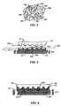
- an exemplary release layer 39is formed from perfluoro silane containing molecules 40 sold under the trade-names FLUOROSYLTM FSD 2500 and FLUOROSYLTM FSD 4500, which are available from Cytonix Corporation located in Beltsville, Maryland and are perfluoether di-functional trimethoxy silane molecules.
- the perfluoro silane molecules 40connect to surface 14 a at bonding regions 42 forming covalent bonds included in covalent bonding group 43 , as well as defining contact regions 44 that include a chain of fluorine molecules extending between spaced-apart bonding groups 43 .
- Covalent bonding group 43fixedly attaches di-functional perfluoro silane molecules 40 to surface 14 a .
- Contact regions 44are positioned to be selectively placed in contact with imprinting layer 34 .
- bonding regions 42are dependent upon, inter alia, the material from which surface 14 a is formed.
- surface 14 ais formed from silicon, Si, and typically has a hydroxyl group bonded thereto.
- the hydroxyl groupresults from cleaning imprint device 28 with a strong acid-oxidizing solution.
- bonding regions 42include silicon-hydroxyl groups 46 .
- the chemical characteristics of bonding groups 48 of the perfluoro silane containing molecules 40are also dependent upon the perfluoro silane molecule employed, which, in the present example, is an ethoxyl group.
- groups 46 and groups 48react to covalently bond perfluoro silane containing molecules 40 to surface 14 a through a condensation reaction vis-á-vis formation of covalent bonding groups 43 .
- FIG. 8hydrogen binding occurs between the covalent bonding group 43 and the silicon-hdroxyl groups 46 .
- the condensation reactionthe covalent bond Si—O—Si is formed.
- FIG.10illustrates an Si—O—Si covalent bond that was formed through the condensation reaction.
- one process employed to create release layer 39includes immersing substrate 26 into a liquid solution (not shown) of perfluoro silane containing molecules 40 at step 100 .
- the solutionincludes a fluorinated solvent, such as C 5 F 13 C 2 H 4 SiCl 3 .
- the molarity of the perfluoro silane containing molecules 40 in solutionis in the range of 0.1 to 1 millimolar.
- substrate 26remains in the solution for a time sufficient to leave a film of the perfluoro silane containing molecules 40 upon surface 14 a once substrate 26 is removed therefrom. In the present example, substrate 26 is immersed into the solution for a period of 1 to 15 minutes.
- step 104substrate 26 is removed from the solution.
- step 106the film of perfluoro silane containing molecules 40 is annealed at a temperature in a range of 100° Celsius to 150° Celsius for a period of time ranging from 20 to 40 minutes. This may be done by placing substrate 26 in an oven or other thermally controlled environment.
- release layer 39is formed to have a monomolecular structure, i.e., the thickness of release layer 39 is approximately equal to a length of one molecule of perfluoro silane containing molecules 40 .
- Perfluoro silane containing molecules 40 in release layer 39form a wetting angle with respect to surface 14 a in a range of 90°-115°.
- the wetting angleis employed as a measure of the suitability of release layer 39 . Specifically, were the wetting angle to fall outside of the aforementioned range, release layer 39 would be considered unsuitable for use in imprint lithography. As a result, either imprint device 28 would be discarded or provided with a new release layer 39 . As a result, by periodically measuring the wetting angle, the operational life of imprint device 28 may be determined.
- one manner in which to increase the operational life of imprint device 28is to form release layer 39 from a mixture of di-functional and mono-functional perfluoro silane containing molecules. It is believed that the characteristics of di-functional molecules results in an undesirable number of unreacted bonding regions, shown as 54 .
- the unreacted bonding regions 54are often positioned between covalent bonding groups 43 and are, therefore, located between opposed ends of di-functional molecules 40 and surface 14 a.
- mono-functional perfluoro silane containing molecules 60are smaller in size than the di-functional perfluoro silane containing molecules 40 . It is believed that the relative smallness of the mono-functional perfluoro silane containing molecules 60 allows the same to attach to silicon groups of un-reacted bonding regions 54 . This results in greater coverage of surface 14 a of imprint device 28 with perfluoro silane containing molecules.
- the mono-functional perfluoro containing molecules 60may include molecules from the following chemical families: mono-functional perfluoro chlorosilanes, mono-functional perfluoro methoxysilanes, and mono-functional perfluoro ethoxysilanes.
- Exemplary mono-functional perfluoro containing molecules 60 employedhave the following general formula R 3 Si(CH 2 ) N (CF 2 ) m CF 3 , where R 3 is a Cl atom, an OCH 3 group, or a OCH 2 CH 3 group and N and M are integers.
- a specific example of mono-functional perfluoro containing molecules 60is tridecafluoro-1,1,2,2-tetrahydrooctyl trichlorosilane and FM660 from Cytnoix Corporation of Beltsville, Md.
- Release layer 39shown in FIG. 6 , may formed from a mixture of di-functional and mono-functional perfluoro containing molecules and applied to imprint device 28 as described above, with respect to FIG. 9 .
- the liquid solutiondiffers only in that it contains a 1:1. mixture of the di-functional and mono-functional perfluoro silane molecules.
Landscapes
- Engineering & Computer Science (AREA)
- Chemical & Material Sciences (AREA)
- Nanotechnology (AREA)
- Physics & Mathematics (AREA)
- General Physics & Mathematics (AREA)
- Manufacturing & Machinery (AREA)
- Crystallography & Structural Chemistry (AREA)
- Microelectronics & Electronic Packaging (AREA)
- Condensed Matter Physics & Semiconductors (AREA)
- Mathematical Physics (AREA)
- Theoretical Computer Science (AREA)
- Architecture (AREA)
- Structural Engineering (AREA)
- Exposure Of Semiconductors, Excluding Electron Or Ion Beam Exposure (AREA)
- Shaping Of Tube Ends By Bending Or Straightening (AREA)
Abstract
Description
0>θ1<75°
With these two characteristics being satisfied, imprinting
Claims (9)

Priority Applications (1)
| Application Number | Priority Date | Filing Date | Title |
|---|---|---|---|
| US10/375,817US7452574B2 (en) | 2003-02-27 | 2003-02-27 | Method to reduce adhesion between a polymerizable layer and a substrate employing a fluorine-containing layer |
Applications Claiming Priority (1)
| Application Number | Priority Date | Filing Date | Title |
|---|---|---|---|
| US10/375,817US7452574B2 (en) | 2003-02-27 | 2003-02-27 | Method to reduce adhesion between a polymerizable layer and a substrate employing a fluorine-containing layer |
Publications (2)
| Publication Number | Publication Date |
|---|---|
| US20040170770A1 US20040170770A1 (en) | 2004-09-02 |
| US7452574B2true US7452574B2 (en) | 2008-11-18 |
Family
ID=32907872
Family Applications (1)
| Application Number | Title | Priority Date | Filing Date |
|---|---|---|---|
| US10/375,817Expired - LifetimeUS7452574B2 (en) | 2003-02-27 | 2003-02-27 | Method to reduce adhesion between a polymerizable layer and a substrate employing a fluorine-containing layer |
Country Status (1)
| Country | Link |
|---|---|
| US (1) | US7452574B2 (en) |
Cited By (3)
| Publication number | Priority date | Publication date | Assignee | Title |
|---|---|---|---|---|
| US20100237042A1 (en)* | 2009-03-23 | 2010-09-23 | Intevac, Inc. | Process for optimization of island to trench ratio in patterned media |
| US8431955B2 (en) | 2010-07-21 | 2013-04-30 | International Business Machines Corporation | Method and structure for balancing power and performance using fluorine and nitrogen doped substrates |
| US10156786B2 (en) | 2015-09-30 | 2018-12-18 | Thomas E. Seidel | Method and structure for nanoimprint lithography masks using optical film coatings |
Families Citing this family (28)
| Publication number | Priority date | Publication date | Assignee | Title |
|---|---|---|---|---|
| US6334960B1 (en)* | 1999-03-11 | 2002-01-01 | Board Of Regents, The University Of Texas System | Step and flash imprint lithography |
| US7442336B2 (en)* | 2003-08-21 | 2008-10-28 | Molecular Imprints, Inc. | Capillary imprinting technique |
| US7077992B2 (en)* | 2002-07-11 | 2006-07-18 | Molecular Imprints, Inc. | Step and repeat imprint lithography processes |
| US7019819B2 (en) | 2002-11-13 | 2006-03-28 | Molecular Imprints, Inc. | Chucking system for modulating shapes of substrates |
| US8349241B2 (en) | 2002-10-04 | 2013-01-08 | Molecular Imprints, Inc. | Method to arrange features on a substrate to replicate features having minimal dimensional variability |
| US6871558B2 (en) | 2002-12-12 | 2005-03-29 | Molecular Imprints, Inc. | Method for determining characteristics of substrate employing fluid geometries |
| US7365103B2 (en)* | 2002-12-12 | 2008-04-29 | Board Of Regents, The University Of Texas System | Compositions for dark-field polymerization and method of using the same for imprint lithography processes |
| US7452574B2 (en) | 2003-02-27 | 2008-11-18 | Molecular Imprints, Inc. | Method to reduce adhesion between a polymerizable layer and a substrate employing a fluorine-containing layer |
| US7122079B2 (en) | 2004-02-27 | 2006-10-17 | Molecular Imprints, Inc. | Composition for an etching mask comprising a silicon-containing material |
| US20060108710A1 (en)* | 2004-11-24 | 2006-05-25 | Molecular Imprints, Inc. | Method to reduce adhesion between a conformable region and a mold |
| US7157036B2 (en) | 2003-06-17 | 2007-01-02 | Molecular Imprints, Inc | Method to reduce adhesion between a conformable region and a pattern of a mold |
| US7307118B2 (en) | 2004-11-24 | 2007-12-11 | Molecular Imprints, Inc. | Composition to reduce adhesion between a conformable region and a mold |
| US7136150B2 (en) | 2003-09-25 | 2006-11-14 | Molecular Imprints, Inc. | Imprint lithography template having opaque alignment marks |
| US7122482B2 (en) | 2003-10-27 | 2006-10-17 | Molecular Imprints, Inc. | Methods for fabricating patterned features utilizing imprint lithography |
| US8076386B2 (en) | 2004-02-23 | 2011-12-13 | Molecular Imprints, Inc. | Materials for imprint lithography |
| US7906180B2 (en) | 2004-02-27 | 2011-03-15 | Molecular Imprints, Inc. | Composition for an etching mask comprising a silicon-containing material |
| US7939131B2 (en) | 2004-08-16 | 2011-05-10 | Molecular Imprints, Inc. | Method to provide a layer with uniform etch characteristics |
| US20060062922A1 (en) | 2004-09-23 | 2006-03-23 | Molecular Imprints, Inc. | Polymerization technique to attenuate oxygen inhibition of solidification of liquids and composition therefor |
| US20060081557A1 (en)* | 2004-10-18 | 2006-04-20 | Molecular Imprints, Inc. | Low-k dielectric functional imprinting materials |
| EP1820619A4 (en)* | 2004-11-30 | 2010-07-07 | Asahi Glass Co Ltd | MOLD AND METHOD FOR MANUFACTURING SUBSTRATES HAVING MICROMOTIVES TRANSFERRED THEREON |
| US8808808B2 (en) | 2005-07-22 | 2014-08-19 | Molecular Imprints, Inc. | Method for imprint lithography utilizing an adhesion primer layer |
| US7759407B2 (en) | 2005-07-22 | 2010-07-20 | Molecular Imprints, Inc. | Composition for adhering materials together |
| US8557351B2 (en)* | 2005-07-22 | 2013-10-15 | Molecular Imprints, Inc. | Method for adhering materials together |
| US8142703B2 (en)* | 2005-10-05 | 2012-03-27 | Molecular Imprints, Inc. | Imprint lithography method |
| US20070138699A1 (en)* | 2005-12-21 | 2007-06-21 | Asml Netherlands B.V. | Imprint lithography |
| US8142702B2 (en)* | 2007-06-18 | 2012-03-27 | Molecular Imprints, Inc. | Solvent-assisted layer formation for imprint lithography |
| JP4706878B2 (en)* | 2008-11-17 | 2011-06-22 | 信越化学工業株式会社 | Plate for micro contact printing |
| WO2012132970A1 (en)* | 2011-03-30 | 2012-10-04 | 富士フイルム株式会社 | Printed circuit board, manufacturing method therefor, and metal-surface treatment liquid |
Citations (252)
| Publication number | Priority date | Publication date | Assignee | Title |
|---|---|---|---|---|
| US3527062A (en) | 1968-09-25 | 1970-09-08 | Singer General Precision | Universal joint flexure hinge |
| US3783520A (en) | 1970-09-28 | 1974-01-08 | Bell Telephone Labor Inc | High accuracy alignment procedure utilizing moire patterns |
| US3807029A (en) | 1972-09-05 | 1974-04-30 | Bendix Corp | Method of making a flexural pivot |
| US3807027A (en) | 1972-03-31 | 1974-04-30 | Johns Manville | Method of forming the bell end of a bell and spigot joint |
| US3811665A (en) | 1972-09-05 | 1974-05-21 | Bendix Corp | Flexural pivot with diaphragm means |
| US4062600A (en) | 1976-04-05 | 1977-12-13 | Litton Systems, Inc. | Dual-gimbal gyroscope flexure suspension |
| US4070116A (en) | 1975-06-23 | 1978-01-24 | International Business Machines Corporation | Gap measuring device for defining the distance between two or more surfaces |
| US4098001A (en) | 1976-10-13 | 1978-07-04 | The Charles Stark Draper Laboratory, Inc. | Remote center compliance system |
| DE2800476A1 (en) | 1977-01-07 | 1978-07-13 | Instruments Sa | Mass prodn. method for grids, graticules etc. - using revolving drum, belt carrying resin and UV light source for polymerisation process |
| US4119688A (en) | 1975-11-03 | 1978-10-10 | International Business Machines Corporation | Electro-lithography method |
| US4155169A (en) | 1978-03-16 | 1979-05-22 | The Charles Stark Draper Laboratory, Inc. | Compliant assembly system device |
| US4201800A (en) | 1978-04-28 | 1980-05-06 | International Business Machines Corp. | Hardened photoresist master image mask process |
| US4202107A (en) | 1978-10-23 | 1980-05-13 | Watson Paul C | Remote axis admittance system |
| JPS5588332U (en) | 1978-12-05 | 1980-06-18 | ||
| US4267212A (en) | 1978-09-20 | 1981-05-12 | Fuji Photo Film Co., Ltd. | Spin coating process |
| JPS577931B2 (en) | 1972-12-23 | 1982-02-13 | ||
| US4326805A (en) | 1980-04-11 | 1982-04-27 | Bell Telephone Laboratories, Incorporated | Method and apparatus for aligning mask and wafer members |
| US4337579A (en) | 1980-04-16 | 1982-07-06 | The Charles Stark Draper Laboratory, Inc. | Deformable remote center compliance device |
| US4355469A (en) | 1980-11-28 | 1982-10-26 | The Charles Stark Draper Laboratory, Inc. | Folded remote center compliance device |
| US4414750A (en) | 1981-10-19 | 1983-11-15 | The Charles Stark Draper Laboratory, Inc. | Single stage remote center compliance device |
| US4426247A (en) | 1982-04-12 | 1984-01-17 | Nippon Telegraph & Telephone Public Corporation | Method for forming micropattern |
| US4440804A (en) | 1982-08-02 | 1984-04-03 | Fairchild Camera & Instrument Corporation | Lift-off process for fabricating self-aligned contacts |
| US4451507A (en) | 1982-10-29 | 1984-05-29 | Rca Corporation | Automatic liquid dispensing apparatus for spinning surface of uniform thickness |
| US4507331A (en) | 1983-12-12 | 1985-03-26 | International Business Machines Corporation | Dry process for forming positive tone micro patterns |
| US4544572A (en) | 1982-09-07 | 1985-10-01 | Minnesota Mining And Manufacturing Company | Coated ophthalmic lenses and method for coating the same |
| US4552833A (en) | 1984-05-14 | 1985-11-12 | International Business Machines Corporation | Radiation sensitive and oxygen plasma developable resist |
| US4552832A (en) | 1982-03-06 | 1985-11-12 | Braun Aktiengesellschaft | Shear foil having protrusions on its skin-contacting surface thereof |
| US4600309A (en) | 1982-12-30 | 1986-07-15 | Thomson-Csf | Process and apparatus for theoptical alignment of patterns in two close-up planes in an exposure means incorporating a divergent radiation source |
| US4610442A (en) | 1982-10-19 | 1986-09-09 | Matsushita Electric Industrial Co, Ltd. | Positioning table |
| US4657845A (en) | 1986-01-14 | 1987-04-14 | International Business Machines Corporation | Positive tone oxygen plasma developable photoresist |
| US4687707A (en) | 1984-06-26 | 1987-08-18 | Asahi Glass Company Ltd. | Low reflectance transparent material having antisoiling properties |
| US4692205A (en) | 1986-01-31 | 1987-09-08 | International Business Machines Corporation | Silicon-containing polyimides as oxygen etch stop and dual dielectric coatings |
| US4694703A (en) | 1984-06-28 | 1987-09-22 | Lear Siegler, Inc. | Circumferentially oriented flexure suspension |
| US4707218A (en) | 1986-10-28 | 1987-11-17 | International Business Machines Corporation | Lithographic image size reduction |
| US4724222A (en) | 1986-04-28 | 1988-02-09 | American Telephone And Telegraph Company, At&T Bell Laboratories | Wafer chuck comprising a curved reference surface |
| US4731155A (en) | 1987-04-15 | 1988-03-15 | General Electric Company | Process for forming a lithographic mask |
| US4737425A (en) | 1986-06-10 | 1988-04-12 | International Business Machines Corporation | Patterned resist and process |
| US4763886A (en) | 1986-12-26 | 1988-08-16 | Nippon Thompson Co., Ltd. | XY-positioning table |
| JPS63138730U (en) | 1987-03-03 | 1988-09-13 | ||
| US4808511A (en) | 1987-05-19 | 1989-02-28 | International Business Machines Corporation | Vapor phase photoresist silylation process |
| US4826943A (en) | 1986-07-25 | 1989-05-02 | Oki Electric Industry Co., Ltd. | Negative resist material |
| US4846931A (en) | 1988-03-29 | 1989-07-11 | Bell Communications Research, Inc. | Method for lifting-off epitaxial films |
| US4848911A (en) | 1986-06-11 | 1989-07-18 | Kabushiki Kaisha Toshiba | Method for aligning first and second objects, relative to each other, and apparatus for practicing this method |
| JPH01196749A (en) | 1988-01-30 | 1989-08-08 | Hoya Corp | Manufacture of substrate for optical information recording medium |
| US4857477A (en) | 1986-09-18 | 1989-08-15 | Oki Electric Industry Co., Ltd. | Process for fabricating a semiconductor device |
| US4883561A (en) | 1988-03-29 | 1989-11-28 | Bell Communications Research, Inc. | Lift-off and subsequent bonding of epitaxial films |
| US4891303A (en) | 1988-05-26 | 1990-01-02 | Texas Instruments Incorporated | Trilayer microlithographic process using a silicon-based resist as the middle layer |
| US4908298A (en) | 1985-03-19 | 1990-03-13 | International Business Machines Corporation | Method of creating patterned multilayer films for use in production of semiconductor circuits and systems |
| JPH0292603A (en) | 1988-09-30 | 1990-04-03 | Hoya Corp | Manufacture of data recording board with guide groove |
| US4919748A (en) | 1989-06-30 | 1990-04-24 | At&T Bell Laboratories | Method for tapered etching |
| US4921778A (en) | 1988-07-29 | 1990-05-01 | Shipley Company Inc. | Photoresist pattern fabrication employing chemically amplified metalized material |
| US4929083A (en) | 1986-06-19 | 1990-05-29 | Xerox Corporation | Focus and overlay characterization and optimization for photolithographic exposure |
| US4931351A (en) | 1987-01-12 | 1990-06-05 | Eastman Kodak Company | Bilayer lithographic process |
| JPH0224848Y2 (en) | 1983-07-01 | 1990-07-09 | ||
| EP0244884B1 (en) | 1986-03-28 | 1990-07-25 | Koninklijke Philips Electronics N.V. | Method of providing a mould with a release layer |
| US4959252A (en) | 1986-09-29 | 1990-09-25 | Rhone-Poulenc Chimie | Highly oriented thermotropic optical disc member |
| US4964945A (en) | 1988-12-09 | 1990-10-23 | Minnesota Mining And Manufacturing Company | Lift off patterning process on a flexible substrate |
| US4976818A (en) | 1987-10-26 | 1990-12-11 | Matsushita Electric Industrial Co., Ltd. | Fine pattern forming method |
| US4980316A (en) | 1988-07-20 | 1990-12-25 | Siemens Aktiengesellschaft | Method for producing a resist structure on a semiconductor |
| US4999280A (en) | 1989-03-17 | 1991-03-12 | International Business Machines Corporation | Spray silylation of photoresist images |
| JPH0390345A (en) | 1989-09-01 | 1991-04-16 | Asahi Glass Co Ltd | Transparent molding |
| US5053318A (en) | 1989-05-18 | 1991-10-01 | Shipley Company Inc. | Plasma processing with metal mask integration |
| US5063321A (en) | 1988-02-24 | 1991-11-05 | Teldix Gmbh | Torsional vibration drive |
| US5071694A (en) | 1989-02-21 | 1991-12-10 | Kanegafuchi Kagaku Kogyo Kabushiki Kaisha | Multi-layer resist |
| US5072126A (en) | 1990-10-31 | 1991-12-10 | International Business Machines Corporation | Promixity alignment using polarized illumination and double conjugate projection lens |
| US5073230A (en) | 1990-04-17 | 1991-12-17 | Arizona Board Of Regents Acting On Behalf Of Arizona State University | Means and methods of lifting and relocating an epitaxial device layer |
| US5074667A (en) | 1988-08-15 | 1991-12-24 | Sumitomo Heavy Industries Co. Ltd. | Position detector employing a sector fresnel zone plate |
| US5108875A (en) | 1988-07-29 | 1992-04-28 | Shipley Company Inc. | Photoresist pattern fabrication employing chemically amplified metalized material |
| US5110514A (en) | 1989-05-01 | 1992-05-05 | Soane Technologies, Inc. | Controlled casting of a shrinkable material |
| US5126006A (en) | 1990-10-30 | 1992-06-30 | International Business Machines Corp. | Plural level chip masking |
| US5148036A (en) | 1989-07-18 | 1992-09-15 | Canon Kabushiki Kaisha | Multi-axis wafer position detecting system using a mark having optical power |
| US5148037A (en) | 1988-09-09 | 1992-09-15 | Canon Kabushiki Kaisha | Position detecting method and apparatus |
| US5151754A (en) | 1989-10-06 | 1992-09-29 | Kabushiki Kaisha Toshiba | Method and an apparatus for measuring a displacement between two objects and a method and an apparatus for measuring a gap distance between two objects |
| WO1992017883A1 (en) | 1991-03-26 | 1992-10-15 | Lennart Olsson | A method and a device for altering of the angular velocity of a driven rotating media carrier |
| US5169494A (en) | 1989-03-27 | 1992-12-08 | Matsushita Electric Industrial Co., Ltd. | Fine pattern forming method |
| US5173393A (en) | 1989-04-24 | 1992-12-22 | Siemens Aktiengesellschaft | Etch-resistant deep ultraviolet resist process having an aromatic treating step after development |
| US5179863A (en) | 1990-03-05 | 1993-01-19 | Kabushiki Kaisha Toshiba | Method and apparatus for setting the gap distance between a mask and a wafer at a predetermined distance |
| US5198326A (en) | 1990-05-24 | 1993-03-30 | Matsushita Electric Industrial Co., Ltd. | Process for forming fine pattern |
| US5204739A (en) | 1992-02-07 | 1993-04-20 | Karl Suss America, Inc. | Proximity mask alignment using a stored video image |
| US5206983A (en) | 1991-06-24 | 1993-05-04 | Wisconsin Alumni Research Foundation | Method of manufacturing micromechanical devices |
| US5212147A (en) | 1991-05-15 | 1993-05-18 | Hewlett-Packard Company | Method of forming a patterned in-situ high Tc superconductive film |
| US5234793A (en) | 1989-04-24 | 1993-08-10 | Siemens Aktiengesellschaft | Method for dimensionally accurate structure transfer in bilayer technique wherein a treating step with a bulging agent is employed after development |
| US5240550A (en) | 1990-09-21 | 1993-08-31 | U.S. Philips Corp. | Method of forming at least one groove in a substrate layer |
| US5240878A (en) | 1991-04-26 | 1993-08-31 | International Business Machines Corporation | Method for forming patterned films on a substrate |
| US5242711A (en) | 1991-08-16 | 1993-09-07 | Rockwell International Corp. | Nucleation control of diamond films by microlithographic patterning |
| US5244818A (en) | 1992-04-08 | 1993-09-14 | Georgia Tech Research Corporation | Processes for lift-off of thin film materials and for the fabrication of three dimensional integrated circuits |
| US5259926A (en) | 1991-09-24 | 1993-11-09 | Hitachi, Ltd. | Method of manufacturing a thin-film pattern on a substrate |
| US5270984A (en) | 1991-08-26 | 1993-12-14 | Nec Corporation | Displacement amplification mechanism for piezoelectric elements |
| US5277749A (en) | 1991-10-17 | 1994-01-11 | International Business Machines Corporation | Methods and apparatus for relieving stress and resisting stencil delamination when performing lift-off processes that utilize high stress metals and/or multiple evaporation steps |
| US5314731A (en) | 1991-05-17 | 1994-05-24 | Asahi Glass Company Ltd. | Surface-treated substrate |
| US5314772A (en) | 1990-10-09 | 1994-05-24 | Arizona Board Of Regents | High resolution, multi-layer resist for microlithography and method therefor |
| US5318870A (en) | 1989-10-18 | 1994-06-07 | Massachusetts Institute Of Technology | Method of patterning a phenolic polymer film without photoactive additive through exposure to high energy radiation below 225 nm with subsequent organometallic treatment and the associated imaged article |
| US5324683A (en) | 1993-06-02 | 1994-06-28 | Motorola, Inc. | Method of forming a semiconductor structure having an air region |
| US5328810A (en) | 1990-05-07 | 1994-07-12 | Micron Technology, Inc. | Method for reducing, by a factor or 2-N, the minimum masking pitch of a photolithographic process |
| US5330881A (en) | 1989-06-02 | 1994-07-19 | Digital Equipment Corp. | Microlithographic method for producing thick, vertically-walled photoresist patterns |
| US5348616A (en) | 1993-05-03 | 1994-09-20 | Motorola, Inc. | Method for patterning a mold |
| US5362606A (en) | 1989-10-18 | 1994-11-08 | Massachusetts Institute Of Technology | Positive resist pattern formation through focused ion beam exposure and surface barrier silylation |
| US5366851A (en) | 1991-07-23 | 1994-11-22 | At&T Bell Laboratories | Device fabrication process |
| US5374454A (en) | 1990-09-18 | 1994-12-20 | International Business Machines Incorporated | Method for conditioning halogenated polymeric materials and structures fabricated therewith |
| US5376810A (en) | 1992-06-26 | 1994-12-27 | California Institute Of Technology | Growth of delta-doped layers on silicon CCD/S for enhanced ultraviolet response |
| US5380474A (en) | 1993-05-20 | 1995-01-10 | Sandia Corporation | Methods for patterned deposition on a substrate |
| US5392123A (en) | 1991-09-06 | 1995-02-21 | Eastman Kodak Company | Optical monitor for measuring a gap between two rollers |
| US5417802A (en) | 1994-03-18 | 1995-05-23 | At&T Corp. | Integrated circuit manufacturing |
| US5421981A (en) | 1991-06-26 | 1995-06-06 | Ppg Industries, Inc. | Electrochemical sensor storage device |
| US5422295A (en) | 1992-12-10 | 1995-06-06 | Samsung Electronics Co., Ltd. | Method for forming a semiconductor memory device having a vertical multi-layered storage electrode |
| US5424549A (en) | 1991-12-20 | 1995-06-13 | Board Of Supervisors Of Louisiana State University And Agricultural And Mechanical College | Scanning systems for high resolution e-beam and X-ray lithography |
| US5425964A (en) | 1994-07-22 | 1995-06-20 | Rockwell International Corporation | Deposition of multiple layer thin films using a broadband spectral monitor |
| US5425848A (en) | 1993-03-16 | 1995-06-20 | U.S. Philips Corporation | Method of providing a patterned relief of cured photoresist on a flat substrate surface and device for carrying out such a method |
| US5431777A (en) | 1992-09-17 | 1995-07-11 | International Business Machines Corporation | Methods and compositions for the selective etching of silicon |
| US5439766A (en) | 1988-12-30 | 1995-08-08 | International Business Machines Corporation | Composition for photo imaging |
| US5452090A (en) | 1992-04-29 | 1995-09-19 | International Business Machines Corporation | CCD based confocal filtering for improved accuracy in x-ray proximity alignment |
| US5453157A (en) | 1994-05-16 | 1995-09-26 | Texas Instruments Incorporated | Low temperature anisotropic ashing of resist for semiconductor fabrication |
| US5459198A (en)* | 1994-07-29 | 1995-10-17 | E. I. Du Pont De Nemours And Company | Fluoroinfused composites, articles of manufacture formed therefrom, and processes for the preparation thereof |
| US5458520A (en) | 1994-12-13 | 1995-10-17 | International Business Machines Corporation | Method for producing planar field emission structure |
| US5468542A (en) | 1985-12-23 | 1995-11-21 | General Electric Company | Method for production of a coated substrate with controlled surface characteristics |
| US5480047A (en) | 1993-06-04 | 1996-01-02 | Sharp Kabushiki Kaisha | Method for forming a fine resist pattern |
| US5482768A (en) | 1993-05-14 | 1996-01-09 | Asahi Glass Company Ltd. | Surface-treated substrate and process for its production |
| US5512131A (en) | 1993-10-04 | 1996-04-30 | President And Fellows Of Harvard College | Formation of microstamped patterns on surfaces and derivative articles |
| US5515167A (en) | 1994-09-13 | 1996-05-07 | Hughes Aircraft Company | Transparent optical chuck incorporating optical monitoring |
| US5523878A (en) | 1994-06-30 | 1996-06-04 | Texas Instruments Incorporated | Self-assembled monolayer coating for micro-mechanical devices |
| US5545367A (en) | 1992-04-15 | 1996-08-13 | Soane Technologies, Inc. | Rapid prototype three dimensional stereolithography |
| EP0733455A2 (en) | 1995-03-22 | 1996-09-25 | IMM INSTITUT FÜR MIKROTECHNIK GmbH | Mould with ejector means for demoulding objects with a microstructure |
| US5566584A (en) | 1995-08-31 | 1996-10-22 | Beta Squared, Inc. | Flexure support for a fixture positioning device |
| US5633505A (en) | 1995-09-29 | 1997-05-27 | Taiwan Semiconductor Manufacturing Company, Ltd. | Semiconductor wafer incorporating marks for inspecting first layer overlay shift in global alignment process |
| US5654238A (en) | 1995-08-03 | 1997-08-05 | International Business Machines Corporation | Method for etching vertical contact holes without substrate damage caused by directional etching |
| DE19648844C1 (en) | 1996-11-26 | 1997-09-18 | Jenoptik Jena Gmbh | Forming microstructured components for embossing tool and formable material between chamber walls |
| US5669303A (en) | 1996-03-04 | 1997-09-23 | Motorola | Apparatus and method for stamping a surface |
| US5670415A (en) | 1994-05-24 | 1997-09-23 | Depositech, Inc. | Method and apparatus for vacuum deposition of highly ionized media in an electromagnetic controlled environment |
| JPH09278490A (en) | 1996-04-11 | 1997-10-28 | Matsushita Electric Ind Co Ltd | Water repellent glass coat and method for producing the same |
| US5700626A (en) | 1994-01-12 | 1997-12-23 | Lg Semicon Co., Ltd. | Method for forming multi-layer resist pattern |
| US5724145A (en) | 1995-07-17 | 1998-03-03 | Seiko Epson Corporation | Optical film thickness measurement method, film formation method, and semiconductor laser fabrication method |
| US5723242A (en)* | 1996-03-28 | 1998-03-03 | Minnesota Mining And Manufacturing Company | Perfluoroether release coatings for organic photoreceptors |
| US5723176A (en) | 1994-03-02 | 1998-03-03 | Telecommunications Research Laboratories | Method and apparatus for making optical components by direct dispensing of curable liquid |
| US5725788A (en) | 1996-03-04 | 1998-03-10 | Motorola | Apparatus and method for patterning a surface |
| WO1998010121A1 (en) | 1996-09-06 | 1998-03-12 | Obducat Ab | Method for anisotropic etching of structures in conducting materials |
| US5736424A (en) | 1987-02-27 | 1998-04-07 | Lucent Technologies Inc. | Device fabrication involving planarization |
| US5743998A (en) | 1995-04-19 | 1998-04-28 | Park Scientific Instruments | Process for transferring microminiature patterns using spin-on glass resist media |
| US5747102A (en) | 1995-11-16 | 1998-05-05 | Nordson Corporation | Method and apparatus for dispensing small amounts of liquid material |
| US5753014A (en) | 1993-11-12 | 1998-05-19 | Van Rijn; Cornelis Johannes Maria | Membrane filter and a method of manufacturing the same as well as a membrane |
| US5760500A (en) | 1996-03-28 | 1998-06-02 | Nippon Thompson Co., Ltd. | XY table using a linear electromagnetic actuator |
| US5772905A (en) | 1995-11-15 | 1998-06-30 | Regents Of The University Of Minnesota | Nanoimprint lithography |
| US5776748A (en) | 1993-10-04 | 1998-07-07 | President And Fellows Of Harvard College | Method of formation of microstamped patterns on plates for adhesion of cells and other biological materials, devices and uses therefor |
| US5779799A (en) | 1996-06-21 | 1998-07-14 | Micron Technology, Inc. | Substrate coating apparatus |
| US5802914A (en) | 1996-05-30 | 1998-09-08 | Eastman Kodak Company | Alignment mechanism using flexures |
| US5877036A (en) | 1996-02-29 | 1999-03-02 | Nec Corporation | Overlay measuring method using correlation function |
| US5877861A (en) | 1997-11-14 | 1999-03-02 | International Business Machines Corporation | Method for overlay control system |
| US5888650A (en) | 1996-06-03 | 1999-03-30 | Minnesota Mining And Manufacturing Company | Temperature-responsive adhesive article |
| US5895263A (en) | 1996-12-19 | 1999-04-20 | International Business Machines Corporation | Process for manufacture of integrated circuit device |
| US5900160A (en) | 1993-10-04 | 1999-05-04 | President And Fellows Of Harvard College | Methods of etching articles via microcontact printing |
| US5907782A (en) | 1998-08-15 | 1999-05-25 | Acer Semiconductor Manufacturing Inc. | Method of forming a multiple fin-pillar capacitor for a high density dram cell |
| US5912049A (en) | 1997-08-12 | 1999-06-15 | Micron Technology, Inc. | Process liquid dispense method and apparatus |
| US5926690A (en) | 1997-05-28 | 1999-07-20 | Advanced Micro Devices, Inc. | Run-to-run control process for controlling critical dimensions |
| US5937758A (en) | 1997-11-26 | 1999-08-17 | Motorola, Inc. | Micro-contact printing stamp |
| US5942871A (en) | 1994-04-01 | 1999-08-24 | Nikon Corporation | Double flexure support for stage drive coil |
| US5948219A (en) | 1997-05-07 | 1999-09-07 | Advanced Micro Devices, Inc. | Apparatus for selectively exposing a semiconductor topography to an electric field |
| US5948470A (en) | 1997-04-28 | 1999-09-07 | Harrison; Christopher | Method of nanoscale patterning and products made thereby |
| US5948570A (en) | 1995-05-26 | 1999-09-07 | Lucent Technologies Inc. | Process for dry lithographic etching |
| WO1999045753A1 (en) | 1998-03-05 | 1999-09-10 | Obducat Ab | Method for manufacturing a resistor |
| US5952127A (en) | 1991-08-22 | 1999-09-14 | Nec Corporation | Method of fabricating a phase shifting reticle |
| WO1999063535A1 (en) | 1998-05-29 | 1999-12-09 | Obducat Aktiebolag | Raw matrix for optical storage media and a method of manufacturing such a matrix |
| US6033977A (en) | 1997-06-30 | 2000-03-07 | Siemens Aktiengesellschaft | Dual damascene structure |
| US6038280A (en) | 1997-03-13 | 2000-03-14 | Helmut Fischer Gmbh & Co. Institut Fur Electronik Und Messtechnik | Method and apparatus for measuring the thicknesses of thin layers by means of x-ray fluorescence |
| US6039897A (en) | 1996-08-28 | 2000-03-21 | University Of Washington | Multiple patterned structures on a single substrate fabricated by elastomeric micro-molding techniques |
| US6046056A (en) | 1996-06-28 | 2000-04-04 | Caliper Technologies Corporation | High throughput screening assay systems in microscale fluidic devices |
| US6051345A (en) | 1998-04-27 | 2000-04-18 | United Microelectronics Corp. | Method of producing phase shifting mask |
| WO2000021689A1 (en) | 1998-10-09 | 2000-04-20 | The Trustees Of Princeton University | Microscale patterning and articles formed thereby |
| US6074827A (en) | 1996-07-30 | 2000-06-13 | Aclara Biosciences, Inc. | Microfluidic method for nucleic acid purification and processing |
| US6091485A (en) | 1999-12-15 | 2000-07-18 | N & K Technology, Inc. | Method and apparatus for optically determining physical parameters of underlayers |
| US6096655A (en) | 1998-09-02 | 2000-08-01 | International Business Machines, Corporation | Method for forming vias and trenches in an insulation layer for a dual-damascene multilevel interconnection structure |
| US6117708A (en) | 1998-02-05 | 2000-09-12 | Micron Technology, Inc. | Use of residual organic compounds to facilitate gate break on a carrier substrate for a semiconductor device |
| US6125183A (en) | 1995-10-30 | 2000-09-26 | Obducat Ab | Cryptosystem for optical storage |
| US6128085A (en) | 1997-12-09 | 2000-10-03 | N & K Technology, Inc. | Reflectance spectroscopic apparatus with toroidal mirrors |
| US6143412A (en) | 1997-02-10 | 2000-11-07 | President And Fellows Of Harvard College | Fabrication of carbon microstructures |
| US6150680A (en) | 1998-03-05 | 2000-11-21 | Welch Allyn, Inc. | Field effect semiconductor device having dipole barrier |
| US6150231A (en) | 1998-06-15 | 2000-11-21 | Siemens Aktiengesellschaft | Overlay measurement technique using moire patterns |
| US6168845B1 (en) | 1999-01-19 | 2001-01-02 | International Business Machines Corporation | Patterned magnetic media and method of making the same using selective oxidation |
| US6180239B1 (en) | 1993-10-04 | 2001-01-30 | President And Fellows Of Harvard College | Microcontact printing on surfaces and derivative articles |
| US6188150B1 (en) | 1999-06-16 | 2001-02-13 | Euv, Llc | Light weight high-stiffness stage platen |
| US6204922B1 (en) | 1998-12-11 | 2001-03-20 | Filmetrics, Inc. | Rapid and accurate thin film measurement of individual layers in a multi-layered or patterned sample |
| US6218316B1 (en) | 1998-10-22 | 2001-04-17 | Micron Technology, Inc. | Planarization of non-planar surfaces in device fabrication |
| US6245581B1 (en) | 2000-04-19 | 2001-06-12 | Advanced Micro Devices, Inc. | Method and apparatus for control of critical dimension using feedback etch control |
| WO2001047003A2 (en) | 1999-12-23 | 2001-06-28 | University Of Massachusetts | Methods and apparatus for forming submicron patterns on films |
| WO2001053889A1 (en) | 2000-01-21 | 2001-07-26 | Obducat Aktiebolag | A mold for nano imprinting |
| US6274294B1 (en) | 1999-02-03 | 2001-08-14 | Electroformed Stents, Inc. | Cylindrical photolithography exposure process and apparatus |
| WO2001069317A1 (en) | 2000-03-15 | 2001-09-20 | Obducat Ab | Device for transferring a pattern to an object |
| WO2001033232A3 (en) | 1999-11-05 | 2001-09-27 | Ion Diagnostics Inc | Precision stage |
| WO2001079589A1 (en) | 2000-04-13 | 2001-10-25 | Obducat Aktiebolag | Method in and apparatus for etching or plating of substrates |
| WO2001079592A1 (en) | 2000-04-13 | 2001-10-25 | Obducat Aktiebolag | Apparatus and method for electrochemical processing of substrates |
| US6309580B1 (en) | 1995-11-15 | 2001-10-30 | Regents Of The University Of Minnesota | Release surfaces, particularly for use in nanoimprint lithography |
| WO2001090816A1 (en) | 2000-05-24 | 2001-11-29 | Obducat Aktiebolag | Method in connection with the production of a template and the template thus produced |
| US6326627B1 (en) | 2000-08-02 | 2001-12-04 | Archimedes Technology Group, Inc. | Mass filtering sputtered ion source |
| US6329256B1 (en) | 1999-09-24 | 2001-12-11 | Advanced Micro Devices, Inc. | Self-aligned damascene gate formation with low gate resistance |
| US6334960B1 (en) | 1999-03-11 | 2002-01-01 | Board Of Regents, The University Of Texas System | Step and flash imprint lithography |
| WO2001033300A3 (en) | 1999-10-29 | 2002-01-24 | Regents Board Of | High precision orientation alignment and gap control stages for imprint lithography processes |
| US6355198B1 (en) | 1996-03-15 | 2002-03-12 | President And Fellows Of Harvard College | Method of forming articles including waveguides via capillary micromolding and microtransfer molding |
| US6383928B1 (en) | 1999-09-02 | 2002-05-07 | Texas Instruments Incorporated | Post copper CMP clean |
| US6387783B1 (en) | 1999-04-26 | 2002-05-14 | International Business Machines Corporation | Methods of T-gate fabrication using a hybrid resist |
| US6388253B1 (en) | 1999-06-29 | 2002-05-14 | Applied Materials, Inc. | Integrated critical dimension control for semiconductor device manufacturing |
| US6391798B1 (en) | 1987-02-27 | 2002-05-21 | Agere Systems Guardian Corp. | Process for planarization a semiconductor substrate |
| US6411010B1 (en) | 1999-05-17 | 2002-06-25 | Seiko Instruments Inc. | Piezoelectric actuator |
| US20020093122A1 (en) | 2000-08-01 | 2002-07-18 | Choi Byung J. | Methods for high-precision gap and orientation sensing between a transparent template and substrate for imprint lithography |
| US20020094496A1 (en) | 2000-07-17 | 2002-07-18 | Choi Byung J. | Method and system of automatic fluid dispensing for imprint lithography processes |
| US20020098426A1 (en) | 2000-07-16 | 2002-07-25 | Sreenivasan S. V. | High-resolution overlay alignment methods and systems for imprint lithography |
| US6447919B1 (en) | 1997-02-03 | 2002-09-10 | Cytonix Corporation | Hydrophobic coating compositions, articles coated with said compositions, and processes for manufacturing same |
| US20020132482A1 (en) | 2000-07-18 | 2002-09-19 | Chou Stephen Y. | Fluid pressure imprint lithography |
| US6455411B1 (en) | 2000-09-11 | 2002-09-24 | Texas Instruments Incorporated | Defect and etch rate control in trench etch for dual damascene patterning of low-k dielectrics |
| US20020150398A1 (en) | 2000-08-21 | 2002-10-17 | Choi Byung J. | Flexure based macro motion translation stage |
| US6467761B1 (en) | 1999-06-21 | 2002-10-22 | The United States Of America As Represented By The Secretary Of Commerce | Positioning stage |
| US6489068B1 (en) | 2001-02-21 | 2002-12-03 | Advanced Micro Devices, Inc. | Process for observing overlay errors on lithographic masks |
| US6495624B1 (en) | 1997-02-03 | 2002-12-17 | Cytonix Corporation | Hydrophobic coating compositions, articles coated with said compositions, and processes for manufacturing same |
| US6514672B2 (en) | 1999-06-17 | 2003-02-04 | Taiwan Semiconductor Manufacturing Company | Dry development process for a bi-layer resist system |
| US6518168B1 (en) | 1995-08-18 | 2003-02-11 | President And Fellows Of Harvard College | Self-assembled monolayer directed patterning of surfaces |
| US6534418B1 (en) | 2001-04-30 | 2003-03-18 | Advanced Micro Devices, Inc. | Use of silicon containing imaging layer to define sub-resolution gate structures |
| US6541360B1 (en) | 2001-04-30 | 2003-04-01 | Advanced Micro Devices, Inc. | Bi-layer trim etch process to form integrated circuit gate structures |
| US20030081193A1 (en) | 2001-06-01 | 2003-05-01 | White Donald L. | Holder, system, and process for improving overlay in lithography |
| US20030080471A1 (en) | 2001-10-29 | 2003-05-01 | Chou Stephen Y. | Lithographic method for molding pattern with nanoscale features |
| US6561706B2 (en) | 2001-06-28 | 2003-05-13 | Advanced Micro Devices, Inc. | Critical dimension monitoring from latent image |
| US6565928B2 (en) | 1999-03-08 | 2003-05-20 | Tokyo Electron Limited | Film forming method and film forming apparatus |
| US20030113638A1 (en) | 2001-12-18 | 2003-06-19 | Mancini David P. | Lithographic template and method of formation and use |
| US20030129542A1 (en) | 2001-10-31 | 2003-07-10 | Brewer Science, Inc. | Contact planarization materials that generate no volatile byproducts or residue during curing |
| US6632742B2 (en) | 2001-04-18 | 2003-10-14 | Promos Technologies Inc. | Method for avoiding defects produced in the CMP process |
| US6635581B2 (en) | 2001-06-08 | 2003-10-21 | Au Optronics, Corp. | Method for forming a thin-film transistor |
| US20030205658A1 (en) | 2002-05-01 | 2003-11-06 | Molecular Imprints, Inc. | Methods of inspecting a lithography template |
| US6646662B1 (en) | 1998-05-26 | 2003-11-11 | Seiko Epson Corporation | Patterning method, patterning apparatus, patterning template, and method for manufacturing the patterning template |
| US20030215577A1 (en) | 2002-05-16 | 2003-11-20 | Willson Carlton Grant | Method and system for fabricating nanoscale patterns in light curable compositions using an electric field |
| US20030235787A1 (en) | 2002-06-24 | 2003-12-25 | Watts Michael P.C. | Low viscosity high resolution patterning material |
| US20040010341A1 (en) | 2002-07-09 | 2004-01-15 | Watts Michael P.C. | System and method for dispensing liquids |
| US20040008334A1 (en) | 2002-07-11 | 2004-01-15 | Sreenivasan Sidlgata V. | Step and repeat imprint lithography systems |
| US20040009673A1 (en) | 2002-07-11 | 2004-01-15 | Sreenivasan Sidlgata V. | Method and system for imprint lithography using an electric field |
| US20040029041A1 (en) | 2002-02-27 | 2004-02-12 | Brewer Science, Inc. | Novel planarization method for multi-layer lithography processing |
| US6696220B2 (en) | 2000-10-12 | 2004-02-24 | Board Of Regents, The University Of Texas System | Template for room temperature, low pressure micro-and nano-imprint lithography |
| US20040036201A1 (en) | 2000-07-18 | 2004-02-26 | Princeton University | Methods and apparatus of field-induced pressure imprint lithography |
| US6703190B2 (en) | 1999-12-07 | 2004-03-09 | Infineon Technologies Ag | Method for producing resist structures |
| US6713238B1 (en) | 1998-10-09 | 2004-03-30 | Stephen Y. Chou | Microscale patterning and articles formed thereby |
| US6730256B1 (en) | 2000-08-04 | 2004-05-04 | Massachusetts Institute Of Technology | Stereolithographic patterning with interlayer surface modifications |
| US20040090611A1 (en) | 2002-11-13 | 2004-05-13 | Molecular Imprints, Inc. | Chucking system for modulating shapes of substrates |
| US20040089979A1 (en) | 2002-11-13 | 2004-05-13 | Molecular Imprints, Inc. | Method of reducing pattern distortions during imprint lithography processes |
| US6737202B2 (en) | 2002-02-22 | 2004-05-18 | Motorola, Inc. | Method of fabricating a tiered structure using a multi-layered resist stack and use |
| US6743713B2 (en) | 2002-05-15 | 2004-06-01 | Institute Of Microelectronics | Method of forming dual damascene pattern using dual bottom anti-reflective coatings (BARC) |
| US20040112862A1 (en) | 2002-12-12 | 2004-06-17 | Molecular Imprints, Inc. | Planarization composition and method of patterning a substrate using the same |
| US20040116548A1 (en) | 2002-12-12 | 2004-06-17 | Molecular Imprints, Inc. | Compositions for dark-field polymerization and method of using the same for imprint lithography processes |
| US20040112861A1 (en) | 2002-12-11 | 2004-06-17 | Molecular Imprints, Inc. | Method for modulating shapes of substrates |
| US20040124566A1 (en) | 2002-07-11 | 2004-07-01 | Sreenivasan Sidlgata V. | Step and repeat imprint lithography processes |
| US6767983B1 (en) | 1999-03-30 | 2004-07-27 | Nippon Steel Chemical Co., Ltd. | Silicone resin and photosensitive resin composition containing the same |
| US6770852B1 (en) | 2003-02-27 | 2004-08-03 | Lam Research Corporation | Critical dimension variation compensation across a wafer by means of local wafer temperature control |
| WO2004044651B1 (en) | 2002-11-13 | 2004-08-05 | Molecular Imprints Inc | A chucking system and method for modulating shapes of substrates |
| US6777170B1 (en) | 2000-08-04 | 2004-08-17 | Massachusetts Institute Of Technology | Stereolithographic patterning by variable dose light delivery |
| US6776094B1 (en) | 1993-10-04 | 2004-08-17 | President & Fellows Of Harvard College | Kit For Microcontact Printing |
| US20040170770A1 (en) | 2003-02-27 | 2004-09-02 | Molecular Imprints, Inc. | Method to reduce adhesion between a polymerizable layer and a substrate employing a fluorine-containing layer |
| US20040168613A1 (en) | 2003-02-27 | 2004-09-02 | Molecular Imprints, Inc. | Composition and method to form a release layer |
| US20040188381A1 (en) | 2003-03-25 | 2004-09-30 | Molecular Imprints, Inc. | Positive tone bi-layer imprint lithography method |
| US20040202865A1 (en) | 2003-04-08 | 2004-10-14 | Andrew Homola | Release coating for stamper |
Family Cites Families (1)
| Publication number | Priority date | Publication date | Assignee | Title |
|---|---|---|---|---|
| US5417402A (en)* | 1994-02-10 | 1995-05-23 | Alliedsignal Inc. | Shutoff and pressure regulating valve |
- 2003
- 2003-02-27USUS10/375,817patent/US7452574B2/ennot_activeExpired - Lifetime
Patent Citations (278)
| Publication number | Priority date | Publication date | Assignee | Title |
|---|---|---|---|---|
| US3527062A (en) | 1968-09-25 | 1970-09-08 | Singer General Precision | Universal joint flexure hinge |
| US3783520A (en) | 1970-09-28 | 1974-01-08 | Bell Telephone Labor Inc | High accuracy alignment procedure utilizing moire patterns |
| US3807027A (en) | 1972-03-31 | 1974-04-30 | Johns Manville | Method of forming the bell end of a bell and spigot joint |
| US3807029A (en) | 1972-09-05 | 1974-04-30 | Bendix Corp | Method of making a flexural pivot |
| US3811665A (en) | 1972-09-05 | 1974-05-21 | Bendix Corp | Flexural pivot with diaphragm means |
| JPS577931B2 (en) | 1972-12-23 | 1982-02-13 | ||
| US4070116A (en) | 1975-06-23 | 1978-01-24 | International Business Machines Corporation | Gap measuring device for defining the distance between two or more surfaces |
| US4119688A (en) | 1975-11-03 | 1978-10-10 | International Business Machines Corporation | Electro-lithography method |
| US4062600A (en) | 1976-04-05 | 1977-12-13 | Litton Systems, Inc. | Dual-gimbal gyroscope flexure suspension |
| US4098001A (en) | 1976-10-13 | 1978-07-04 | The Charles Stark Draper Laboratory, Inc. | Remote center compliance system |
| DE2800476A1 (en) | 1977-01-07 | 1978-07-13 | Instruments Sa | Mass prodn. method for grids, graticules etc. - using revolving drum, belt carrying resin and UV light source for polymerisation process |
| US4155169A (en) | 1978-03-16 | 1979-05-22 | The Charles Stark Draper Laboratory, Inc. | Compliant assembly system device |
| US4201800A (en) | 1978-04-28 | 1980-05-06 | International Business Machines Corp. | Hardened photoresist master image mask process |
| US4267212A (en) | 1978-09-20 | 1981-05-12 | Fuji Photo Film Co., Ltd. | Spin coating process |
| US4202107A (en) | 1978-10-23 | 1980-05-13 | Watson Paul C | Remote axis admittance system |
| JPS5588332U (en) | 1978-12-05 | 1980-06-18 | ||
| US4326805A (en) | 1980-04-11 | 1982-04-27 | Bell Telephone Laboratories, Incorporated | Method and apparatus for aligning mask and wafer members |
| US4337579A (en) | 1980-04-16 | 1982-07-06 | The Charles Stark Draper Laboratory, Inc. | Deformable remote center compliance device |
| US4355469A (en) | 1980-11-28 | 1982-10-26 | The Charles Stark Draper Laboratory, Inc. | Folded remote center compliance device |
| US4414750A (en) | 1981-10-19 | 1983-11-15 | The Charles Stark Draper Laboratory, Inc. | Single stage remote center compliance device |
| US4552832A (en) | 1982-03-06 | 1985-11-12 | Braun Aktiengesellschaft | Shear foil having protrusions on its skin-contacting surface thereof |
| US4426247A (en) | 1982-04-12 | 1984-01-17 | Nippon Telegraph & Telephone Public Corporation | Method for forming micropattern |
| US4440804A (en) | 1982-08-02 | 1984-04-03 | Fairchild Camera & Instrument Corporation | Lift-off process for fabricating self-aligned contacts |
| US4544572B1 (en) | 1982-09-07 | 1994-01-04 | Signet Armorlite, Inc. | |
| US4544572A (en) | 1982-09-07 | 1985-10-01 | Minnesota Mining And Manufacturing Company | Coated ophthalmic lenses and method for coating the same |
| US4610442A (en) | 1982-10-19 | 1986-09-09 | Matsushita Electric Industrial Co, Ltd. | Positioning table |
| US4451507A (en) | 1982-10-29 | 1984-05-29 | Rca Corporation | Automatic liquid dispensing apparatus for spinning surface of uniform thickness |
| US4600309A (en) | 1982-12-30 | 1986-07-15 | Thomson-Csf | Process and apparatus for theoptical alignment of patterns in two close-up planes in an exposure means incorporating a divergent radiation source |
| JPH0224848Y2 (en) | 1983-07-01 | 1990-07-09 | ||
| US4507331A (en) | 1983-12-12 | 1985-03-26 | International Business Machines Corporation | Dry process for forming positive tone micro patterns |
| US4552833A (en) | 1984-05-14 | 1985-11-12 | International Business Machines Corporation | Radiation sensitive and oxygen plasma developable resist |
| US4687707A (en) | 1984-06-26 | 1987-08-18 | Asahi Glass Company Ltd. | Low reflectance transparent material having antisoiling properties |
| US4694703A (en) | 1984-06-28 | 1987-09-22 | Lear Siegler, Inc. | Circumferentially oriented flexure suspension |
| US4908298A (en) | 1985-03-19 | 1990-03-13 | International Business Machines Corporation | Method of creating patterned multilayer films for use in production of semiconductor circuits and systems |
| US5468542A (en) | 1985-12-23 | 1995-11-21 | General Electric Company | Method for production of a coated substrate with controlled surface characteristics |
| US4657845A (en) | 1986-01-14 | 1987-04-14 | International Business Machines Corporation | Positive tone oxygen plasma developable photoresist |
| US4692205A (en) | 1986-01-31 | 1987-09-08 | International Business Machines Corporation | Silicon-containing polyimides as oxygen etch stop and dual dielectric coatings |
| EP0244884B1 (en) | 1986-03-28 | 1990-07-25 | Koninklijke Philips Electronics N.V. | Method of providing a mould with a release layer |
| US4724222A (en) | 1986-04-28 | 1988-02-09 | American Telephone And Telegraph Company, At&T Bell Laboratories | Wafer chuck comprising a curved reference surface |
| US4737425A (en) | 1986-06-10 | 1988-04-12 | International Business Machines Corporation | Patterned resist and process |
| US4848911A (en) | 1986-06-11 | 1989-07-18 | Kabushiki Kaisha Toshiba | Method for aligning first and second objects, relative to each other, and apparatus for practicing this method |
| US4929083A (en) | 1986-06-19 | 1990-05-29 | Xerox Corporation | Focus and overlay characterization and optimization for photolithographic exposure |
| US4826943A (en) | 1986-07-25 | 1989-05-02 | Oki Electric Industry Co., Ltd. | Negative resist material |
| US4857477A (en) | 1986-09-18 | 1989-08-15 | Oki Electric Industry Co., Ltd. | Process for fabricating a semiconductor device |
| US4959252A (en) | 1986-09-29 | 1990-09-25 | Rhone-Poulenc Chimie | Highly oriented thermotropic optical disc member |
| US4707218A (en) | 1986-10-28 | 1987-11-17 | International Business Machines Corporation | Lithographic image size reduction |
| US4763886A (en) | 1986-12-26 | 1988-08-16 | Nippon Thompson Co., Ltd. | XY-positioning table |
| US4931351A (en) | 1987-01-12 | 1990-06-05 | Eastman Kodak Company | Bilayer lithographic process |
| US6391798B1 (en) | 1987-02-27 | 2002-05-21 | Agere Systems Guardian Corp. | Process for planarization a semiconductor substrate |
| US5736424A (en) | 1987-02-27 | 1998-04-07 | Lucent Technologies Inc. | Device fabrication involving planarization |
| JPS63138730U (en) | 1987-03-03 | 1988-09-13 | ||
| US4731155A (en) | 1987-04-15 | 1988-03-15 | General Electric Company | Process for forming a lithographic mask |
| US4808511A (en) | 1987-05-19 | 1989-02-28 | International Business Machines Corporation | Vapor phase photoresist silylation process |
| US4976818A (en) | 1987-10-26 | 1990-12-11 | Matsushita Electric Industrial Co., Ltd. | Fine pattern forming method |
| JPH01196749A (en) | 1988-01-30 | 1989-08-08 | Hoya Corp | Manufacture of substrate for optical information recording medium |
| US5063321A (en) | 1988-02-24 | 1991-11-05 | Teldix Gmbh | Torsional vibration drive |
| US4883561A (en) | 1988-03-29 | 1989-11-28 | Bell Communications Research, Inc. | Lift-off and subsequent bonding of epitaxial films |
| US4846931A (en) | 1988-03-29 | 1989-07-11 | Bell Communications Research, Inc. | Method for lifting-off epitaxial films |
| US4891303A (en) | 1988-05-26 | 1990-01-02 | Texas Instruments Incorporated | Trilayer microlithographic process using a silicon-based resist as the middle layer |
| US4980316A (en) | 1988-07-20 | 1990-12-25 | Siemens Aktiengesellschaft | Method for producing a resist structure on a semiconductor |
| US4921778A (en) | 1988-07-29 | 1990-05-01 | Shipley Company Inc. | Photoresist pattern fabrication employing chemically amplified metalized material |
| US5108875A (en) | 1988-07-29 | 1992-04-28 | Shipley Company Inc. | Photoresist pattern fabrication employing chemically amplified metalized material |
| US5074667A (en) | 1988-08-15 | 1991-12-24 | Sumitomo Heavy Industries Co. Ltd. | Position detector employing a sector fresnel zone plate |
| US5148037A (en) | 1988-09-09 | 1992-09-15 | Canon Kabushiki Kaisha | Position detecting method and apparatus |
| JPH0292603A (en) | 1988-09-30 | 1990-04-03 | Hoya Corp | Manufacture of data recording board with guide groove |
| US4964945A (en) | 1988-12-09 | 1990-10-23 | Minnesota Mining And Manufacturing Company | Lift off patterning process on a flexible substrate |
| US5439766A (en) | 1988-12-30 | 1995-08-08 | International Business Machines Corporation | Composition for photo imaging |
| US5071694A (en) | 1989-02-21 | 1991-12-10 | Kanegafuchi Kagaku Kogyo Kabushiki Kaisha | Multi-layer resist |
| US4999280A (en) | 1989-03-17 | 1991-03-12 | International Business Machines Corporation | Spray silylation of photoresist images |
| US5169494A (en) | 1989-03-27 | 1992-12-08 | Matsushita Electric Industrial Co., Ltd. | Fine pattern forming method |
| US5234793A (en) | 1989-04-24 | 1993-08-10 | Siemens Aktiengesellschaft | Method for dimensionally accurate structure transfer in bilayer technique wherein a treating step with a bulging agent is employed after development |
| US5173393A (en) | 1989-04-24 | 1992-12-22 | Siemens Aktiengesellschaft | Etch-resistant deep ultraviolet resist process having an aromatic treating step after development |
| US5110514A (en) | 1989-05-01 | 1992-05-05 | Soane Technologies, Inc. | Controlled casting of a shrinkable material |
| US5053318A (en) | 1989-05-18 | 1991-10-01 | Shipley Company Inc. | Plasma processing with metal mask integration |
| US5330881A (en) | 1989-06-02 | 1994-07-19 | Digital Equipment Corp. | Microlithographic method for producing thick, vertically-walled photoresist patterns |
| US4919748A (en) | 1989-06-30 | 1990-04-24 | At&T Bell Laboratories | Method for tapered etching |
| US5148036A (en) | 1989-07-18 | 1992-09-15 | Canon Kabushiki Kaisha | Multi-axis wafer position detecting system using a mark having optical power |
| JPH0390345A (en) | 1989-09-01 | 1991-04-16 | Asahi Glass Co Ltd | Transparent molding |
| US5151754A (en) | 1989-10-06 | 1992-09-29 | Kabushiki Kaisha Toshiba | Method and an apparatus for measuring a displacement between two objects and a method and an apparatus for measuring a gap distance between two objects |
| US5318870A (en) | 1989-10-18 | 1994-06-07 | Massachusetts Institute Of Technology | Method of patterning a phenolic polymer film without photoactive additive through exposure to high energy radiation below 225 nm with subsequent organometallic treatment and the associated imaged article |
| US5362606A (en) | 1989-10-18 | 1994-11-08 | Massachusetts Institute Of Technology | Positive resist pattern formation through focused ion beam exposure and surface barrier silylation |
| US5179863A (en) | 1990-03-05 | 1993-01-19 | Kabushiki Kaisha Toshiba | Method and apparatus for setting the gap distance between a mask and a wafer at a predetermined distance |
| US5073230A (en) | 1990-04-17 | 1991-12-17 | Arizona Board Of Regents Acting On Behalf Of Arizona State University | Means and methods of lifting and relocating an epitaxial device layer |
| US5328810A (en) | 1990-05-07 | 1994-07-12 | Micron Technology, Inc. | Method for reducing, by a factor or 2-N, the minimum masking pitch of a photolithographic process |
| US5527662A (en) | 1990-05-24 | 1996-06-18 | Matsushita Electric Industrial Co., Ltd. | Process for forming fine pattern |
| US5198326A (en) | 1990-05-24 | 1993-03-30 | Matsushita Electric Industrial Co., Ltd. | Process for forming fine pattern |
| US5374454A (en) | 1990-09-18 | 1994-12-20 | International Business Machines Incorporated | Method for conditioning halogenated polymeric materials and structures fabricated therewith |
| US5240550A (en) | 1990-09-21 | 1993-08-31 | U.S. Philips Corp. | Method of forming at least one groove in a substrate layer |
| US5314772A (en) | 1990-10-09 | 1994-05-24 | Arizona Board Of Regents | High resolution, multi-layer resist for microlithography and method therefor |
| US5126006A (en) | 1990-10-30 | 1992-06-30 | International Business Machines Corp. | Plural level chip masking |
| US5072126A (en) | 1990-10-31 | 1991-12-10 | International Business Machines Corporation | Promixity alignment using polarized illumination and double conjugate projection lens |
| WO1992017883A1 (en) | 1991-03-26 | 1992-10-15 | Lennart Olsson | A method and a device for altering of the angular velocity of a driven rotating media carrier |
| US5240878A (en) | 1991-04-26 | 1993-08-31 | International Business Machines Corporation | Method for forming patterned films on a substrate |
| US5212147A (en) | 1991-05-15 | 1993-05-18 | Hewlett-Packard Company | Method of forming a patterned in-situ high Tc superconductive film |
| US5314731A (en) | 1991-05-17 | 1994-05-24 | Asahi Glass Company Ltd. | Surface-treated substrate |
| US5206983A (en) | 1991-06-24 | 1993-05-04 | Wisconsin Alumni Research Foundation | Method of manufacturing micromechanical devices |
| US5421981A (en) | 1991-06-26 | 1995-06-06 | Ppg Industries, Inc. | Electrochemical sensor storage device |
| US5366851A (en) | 1991-07-23 | 1994-11-22 | At&T Bell Laboratories | Device fabrication process |
| US5242711A (en) | 1991-08-16 | 1993-09-07 | Rockwell International Corp. | Nucleation control of diamond films by microlithographic patterning |
| US5952127A (en) | 1991-08-22 | 1999-09-14 | Nec Corporation | Method of fabricating a phase shifting reticle |
| US5270984A (en) | 1991-08-26 | 1993-12-14 | Nec Corporation | Displacement amplification mechanism for piezoelectric elements |
| US5392123A (en) | 1991-09-06 | 1995-02-21 | Eastman Kodak Company | Optical monitor for measuring a gap between two rollers |
| US5259926A (en) | 1991-09-24 | 1993-11-09 | Hitachi, Ltd. | Method of manufacturing a thin-film pattern on a substrate |
| US5277749A (en) | 1991-10-17 | 1994-01-11 | International Business Machines Corporation | Methods and apparatus for relieving stress and resisting stencil delamination when performing lift-off processes that utilize high stress metals and/or multiple evaporation steps |
| US5424549A (en) | 1991-12-20 | 1995-06-13 | Board Of Supervisors Of Louisiana State University And Agricultural And Mechanical College | Scanning systems for high resolution e-beam and X-ray lithography |
| US5204739A (en) | 1992-02-07 | 1993-04-20 | Karl Suss America, Inc. | Proximity mask alignment using a stored video image |
| US5244818A (en) | 1992-04-08 | 1993-09-14 | Georgia Tech Research Corporation | Processes for lift-off of thin film materials and for the fabrication of three dimensional integrated circuits |
| US5545367A (en) | 1992-04-15 | 1996-08-13 | Soane Technologies, Inc. | Rapid prototype three dimensional stereolithography |
| US5452090A (en) | 1992-04-29 | 1995-09-19 | International Business Machines Corporation | CCD based confocal filtering for improved accuracy in x-ray proximity alignment |
| US5376810A (en) | 1992-06-26 | 1994-12-27 | California Institute Of Technology | Growth of delta-doped layers on silicon CCD/S for enhanced ultraviolet response |
| US5431777A (en) | 1992-09-17 | 1995-07-11 | International Business Machines Corporation | Methods and compositions for the selective etching of silicon |
| US5422295A (en) | 1992-12-10 | 1995-06-06 | Samsung Electronics Co., Ltd. | Method for forming a semiconductor memory device having a vertical multi-layered storage electrode |
| US5425848A (en) | 1993-03-16 | 1995-06-20 | U.S. Philips Corporation | Method of providing a patterned relief of cured photoresist on a flat substrate surface and device for carrying out such a method |
| US5348616A (en) | 1993-05-03 | 1994-09-20 | Motorola, Inc. | Method for patterning a mold |
| US5482768A (en) | 1993-05-14 | 1996-01-09 | Asahi Glass Company Ltd. | Surface-treated substrate and process for its production |
| US5380474A (en) | 1993-05-20 | 1995-01-10 | Sandia Corporation | Methods for patterned deposition on a substrate |
| US5324683A (en) | 1993-06-02 | 1994-06-28 | Motorola, Inc. | Method of forming a semiconductor structure having an air region |
| US5480047A (en) | 1993-06-04 | 1996-01-02 | Sharp Kabushiki Kaisha | Method for forming a fine resist pattern |
| US6776094B1 (en) | 1993-10-04 | 2004-08-17 | President & Fellows Of Harvard College | Kit For Microcontact Printing |
| US5900160A (en) | 1993-10-04 | 1999-05-04 | President And Fellows Of Harvard College | Methods of etching articles via microcontact printing |
| US5512131A (en) | 1993-10-04 | 1996-04-30 | President And Fellows Of Harvard College | Formation of microstamped patterns on surfaces and derivative articles |
| US5776748A (en) | 1993-10-04 | 1998-07-07 | President And Fellows Of Harvard College | Method of formation of microstamped patterns on plates for adhesion of cells and other biological materials, devices and uses therefor |
| US6180239B1 (en) | 1993-10-04 | 2001-01-30 | President And Fellows Of Harvard College | Microcontact printing on surfaces and derivative articles |
| US5753014A (en) | 1993-11-12 | 1998-05-19 | Van Rijn; Cornelis Johannes Maria | Membrane filter and a method of manufacturing the same as well as a membrane |
| US5700626A (en) | 1994-01-12 | 1997-12-23 | Lg Semicon Co., Ltd. | Method for forming multi-layer resist pattern |
| US5723176A (en) | 1994-03-02 | 1998-03-03 | Telecommunications Research Laboratories | Method and apparatus for making optical components by direct dispensing of curable liquid |
| US5417802A (en) | 1994-03-18 | 1995-05-23 | At&T Corp. | Integrated circuit manufacturing |
| US5942871A (en) | 1994-04-01 | 1999-08-24 | Nikon Corporation | Double flexure support for stage drive coil |
| US5453157A (en) | 1994-05-16 | 1995-09-26 | Texas Instruments Incorporated | Low temperature anisotropic ashing of resist for semiconductor fabrication |
| US5670415A (en) | 1994-05-24 | 1997-09-23 | Depositech, Inc. | Method and apparatus for vacuum deposition of highly ionized media in an electromagnetic controlled environment |
| US6035805A (en) | 1994-05-24 | 2000-03-14 | Depositech, Inc. | Method and apparatus for vacuum deposition of highly ionized media in an electromagnetic controlled environment |
| US5855686A (en) | 1994-05-24 | 1999-01-05 | Depositech, Inc. | Method and apparatus for vacuum deposition of highly ionized media in an electromagnetic controlled environment |
| US5523878A (en) | 1994-06-30 | 1996-06-04 | Texas Instruments Incorporated | Self-assembled monolayer coating for micro-mechanical devices |
| US5425964A (en) | 1994-07-22 | 1995-06-20 | Rockwell International Corporation | Deposition of multiple layer thin films using a broadband spectral monitor |
| US5459198A (en)* | 1994-07-29 | 1995-10-17 | E. I. Du Pont De Nemours And Company | Fluoroinfused composites, articles of manufacture formed therefrom, and processes for the preparation thereof |
| US5515167A (en) | 1994-09-13 | 1996-05-07 | Hughes Aircraft Company | Transparent optical chuck incorporating optical monitoring |
| US5458520A (en) | 1994-12-13 | 1995-10-17 | International Business Machines Corporation | Method for producing planar field emission structure |
| EP0733455A2 (en) | 1995-03-22 | 1996-09-25 | IMM INSTITUT FÜR MIKROTECHNIK GmbH | Mould with ejector means for demoulding objects with a microstructure |
| US5743998A (en) | 1995-04-19 | 1998-04-28 | Park Scientific Instruments | Process for transferring microminiature patterns using spin-on glass resist media |
| US5948570A (en) | 1995-05-26 | 1999-09-07 | Lucent Technologies Inc. | Process for dry lithographic etching |
| US5724145A (en) | 1995-07-17 | 1998-03-03 | Seiko Epson Corporation | Optical film thickness measurement method, film formation method, and semiconductor laser fabrication method |
| US5654238A (en) | 1995-08-03 | 1997-08-05 | International Business Machines Corporation | Method for etching vertical contact holes without substrate damage caused by directional etching |
| US6518168B1 (en) | 1995-08-18 | 2003-02-11 | President And Fellows Of Harvard College | Self-assembled monolayer directed patterning of surfaces |
| US5566584A (en) | 1995-08-31 | 1996-10-22 | Beta Squared, Inc. | Flexure support for a fixture positioning device |
| US5633505A (en) | 1995-09-29 | 1997-05-27 | Taiwan Semiconductor Manufacturing Company, Ltd. | Semiconductor wafer incorporating marks for inspecting first layer overlay shift in global alignment process |
| US6125183A (en) | 1995-10-30 | 2000-09-26 | Obducat Ab | Cryptosystem for optical storage |
| US5772905A (en) | 1995-11-15 | 1998-06-30 | Regents Of The University Of Minnesota | Nanoimprint lithography |
| US6309580B1 (en) | 1995-11-15 | 2001-10-30 | Regents Of The University Of Minnesota | Release surfaces, particularly for use in nanoimprint lithography |
| US5747102A (en) | 1995-11-16 | 1998-05-05 | Nordson Corporation | Method and apparatus for dispensing small amounts of liquid material |
| US5877036A (en) | 1996-02-29 | 1999-03-02 | Nec Corporation | Overlay measuring method using correlation function |
| US5669303A (en) | 1996-03-04 | 1997-09-23 | Motorola | Apparatus and method for stamping a surface |
| US5725788A (en) | 1996-03-04 | 1998-03-10 | Motorola | Apparatus and method for patterning a surface |
| US6355198B1 (en) | 1996-03-15 | 2002-03-12 | President And Fellows Of Harvard College | Method of forming articles including waveguides via capillary micromolding and microtransfer molding |
| US5723242A (en)* | 1996-03-28 | 1998-03-03 | Minnesota Mining And Manufacturing Company | Perfluoroether release coatings for organic photoreceptors |
| US5760500A (en) | 1996-03-28 | 1998-06-02 | Nippon Thompson Co., Ltd. | XY table using a linear electromagnetic actuator |
| JPH09278490A (en) | 1996-04-11 | 1997-10-28 | Matsushita Electric Ind Co Ltd | Water repellent glass coat and method for producing the same |
| US5802914A (en) | 1996-05-30 | 1998-09-08 | Eastman Kodak Company | Alignment mechanism using flexures |
| US5888650A (en) | 1996-06-03 | 1999-03-30 | Minnesota Mining And Manufacturing Company | Temperature-responsive adhesive article |
| US5779799A (en) | 1996-06-21 | 1998-07-14 | Micron Technology, Inc. | Substrate coating apparatus |
| US6046056A (en) | 1996-06-28 | 2000-04-04 | Caliper Technologies Corporation | High throughput screening assay systems in microscale fluidic devices |
| US6074827A (en) | 1996-07-30 | 2000-06-13 | Aclara Biosciences, Inc. | Microfluidic method for nucleic acid purification and processing |
| US6039897A (en) | 1996-08-28 | 2000-03-21 | University Of Washington | Multiple patterned structures on a single substrate fabricated by elastomeric micro-molding techniques |
| WO1998010121A1 (en) | 1996-09-06 | 1998-03-12 | Obducat Ab | Method for anisotropic etching of structures in conducting materials |
| DE19648844C1 (en) | 1996-11-26 | 1997-09-18 | Jenoptik Jena Gmbh | Forming microstructured components for embossing tool and formable material between chamber walls |
| US5895263A (en) | 1996-12-19 | 1999-04-20 | International Business Machines Corporation | Process for manufacture of integrated circuit device |
| US6447919B1 (en) | 1997-02-03 | 2002-09-10 | Cytonix Corporation | Hydrophobic coating compositions, articles coated with said compositions, and processes for manufacturing same |
| US6495624B1 (en) | 1997-02-03 | 2002-12-17 | Cytonix Corporation | Hydrophobic coating compositions, articles coated with said compositions, and processes for manufacturing same |
| US6143412A (en) | 1997-02-10 | 2000-11-07 | President And Fellows Of Harvard College | Fabrication of carbon microstructures |
| US6038280A (en) | 1997-03-13 | 2000-03-14 | Helmut Fischer Gmbh & Co. Institut Fur Electronik Und Messtechnik | Method and apparatus for measuring the thicknesses of thin layers by means of x-ray fluorescence |
| US5948470A (en) | 1997-04-28 | 1999-09-07 | Harrison; Christopher | Method of nanoscale patterning and products made thereby |
| US5948219A (en) | 1997-05-07 | 1999-09-07 | Advanced Micro Devices, Inc. | Apparatus for selectively exposing a semiconductor topography to an electric field |
| US5926690A (en) | 1997-05-28 | 1999-07-20 | Advanced Micro Devices, Inc. | Run-to-run control process for controlling critical dimensions |
| US6033977A (en) | 1997-06-30 | 2000-03-07 | Siemens Aktiengesellschaft | Dual damascene structure |
| US5912049A (en) | 1997-08-12 | 1999-06-15 | Micron Technology, Inc. | Process liquid dispense method and apparatus |
| US5877861A (en) | 1997-11-14 | 1999-03-02 | International Business Machines Corporation | Method for overlay control system |
| US5937758A (en) | 1997-11-26 | 1999-08-17 | Motorola, Inc. | Micro-contact printing stamp |
| US6128085A (en) | 1997-12-09 | 2000-10-03 | N & K Technology, Inc. | Reflectance spectroscopic apparatus with toroidal mirrors |
| US6117708A (en) | 1998-02-05 | 2000-09-12 | Micron Technology, Inc. | Use of residual organic compounds to facilitate gate break on a carrier substrate for a semiconductor device |
| WO1999045753A1 (en) | 1998-03-05 | 1999-09-10 | Obducat Ab | Method for manufacturing a resistor |
| US6150680A (en) | 1998-03-05 | 2000-11-21 | Welch Allyn, Inc. | Field effect semiconductor device having dipole barrier |
| US6051345A (en) | 1998-04-27 | 2000-04-18 | United Microelectronics Corp. | Method of producing phase shifting mask |
| US6646662B1 (en) | 1998-05-26 | 2003-11-11 | Seiko Epson Corporation | Patterning method, patterning apparatus, patterning template, and method for manufacturing the patterning template |
| WO1999063535A1 (en) | 1998-05-29 | 1999-12-09 | Obducat Aktiebolag | Raw matrix for optical storage media and a method of manufacturing such a matrix |
| US6150231A (en) | 1998-06-15 | 2000-11-21 | Siemens Aktiengesellschaft | Overlay measurement technique using moire patterns |
| US20020167117A1 (en) | 1998-06-30 | 2002-11-14 | Regents Of The University Of Minnesota | Release surfaces, particularly for use in nanoimprint lithography |
| US5907782A (en) | 1998-08-15 | 1999-05-25 | Acer Semiconductor Manufacturing Inc. | Method of forming a multiple fin-pillar capacitor for a high density dram cell |
| US6096655A (en) | 1998-09-02 | 2000-08-01 | International Business Machines, Corporation | Method for forming vias and trenches in an insulation layer for a dual-damascene multilevel interconnection structure |
| US6713238B1 (en) | 1998-10-09 | 2004-03-30 | Stephen Y. Chou | Microscale patterning and articles formed thereby |
| WO2000021689A1 (en) | 1998-10-09 | 2000-04-20 | The Trustees Of Princeton University | Microscale patterning and articles formed thereby |
| US6218316B1 (en) | 1998-10-22 | 2001-04-17 | Micron Technology, Inc. | Planarization of non-planar surfaces in device fabrication |
| US6677252B2 (en) | 1998-10-22 | 2004-01-13 | Micron Technology, Inc. | Methods for planarization of non-planar surfaces in device fabrication |
| US6204922B1 (en) | 1998-12-11 | 2001-03-20 | Filmetrics, Inc. | Rapid and accurate thin film measurement of individual layers in a multi-layered or patterned sample |
| US6168845B1 (en) | 1999-01-19 | 2001-01-02 | International Business Machines Corporation | Patterned magnetic media and method of making the same using selective oxidation |
| US6274294B1 (en) | 1999-02-03 | 2001-08-14 | Electroformed Stents, Inc. | Cylindrical photolithography exposure process and apparatus |
| US6565928B2 (en) | 1999-03-08 | 2003-05-20 | Tokyo Electron Limited | Film forming method and film forming apparatus |
| US6719915B2 (en) | 1999-03-11 | 2004-04-13 | Board Of Regents, The University Of Texas System | Step and flash imprint lithography |
| US6334960B1 (en) | 1999-03-11 | 2002-01-01 | Board Of Regents, The University Of Texas System | Step and flash imprint lithography |
| WO2000054107A9 (en) | 1999-03-11 | 2002-05-02 | Univ Texas | Step and flash imprint lithography |
| US6767983B1 (en) | 1999-03-30 | 2004-07-27 | Nippon Steel Chemical Co., Ltd. | Silicone resin and photosensitive resin composition containing the same |
| US6387783B1 (en) | 1999-04-26 | 2002-05-14 | International Business Machines Corporation | Methods of T-gate fabrication using a hybrid resist |
| US6411010B1 (en) | 1999-05-17 | 2002-06-25 | Seiko Instruments Inc. | Piezoelectric actuator |
| US6188150B1 (en) | 1999-06-16 | 2001-02-13 | Euv, Llc | Light weight high-stiffness stage platen |
| US6514672B2 (en) | 1999-06-17 | 2003-02-04 | Taiwan Semiconductor Manufacturing Company | Dry development process for a bi-layer resist system |
| US6467761B1 (en) | 1999-06-21 | 2002-10-22 | The United States Of America As Represented By The Secretary Of Commerce | Positioning stage |
| US6388253B1 (en) | 1999-06-29 | 2002-05-14 | Applied Materials, Inc. | Integrated critical dimension control for semiconductor device manufacturing |
| US6383928B1 (en) | 1999-09-02 | 2002-05-07 | Texas Instruments Incorporated | Post copper CMP clean |
| US6329256B1 (en) | 1999-09-24 | 2001-12-11 | Advanced Micro Devices, Inc. | Self-aligned damascene gate formation with low gate resistance |
| US20040104641A1 (en) | 1999-10-29 | 2004-06-03 | University Of Texas System | Method of separating a template from a substrate during imprint lithography |
| US20040149687A1 (en) | 1999-10-29 | 2004-08-05 | University Of Texas System, Board Of Regents, Ut System | Method of manufacturing a vacuum chuck used in imprint lithography |
| WO2001033300A3 (en) | 1999-10-29 | 2002-01-24 | Regents Board Of | High precision orientation alignment and gap control stages for imprint lithography processes |
| US20040168588A1 (en) | 1999-10-29 | 2004-09-02 | Board Of Regents, The University Of Texas System | Method of orientating a template with respect to a substrate in response to a force exerted on the template |
| US20040169441A1 (en) | 1999-10-29 | 2004-09-02 | The Board Of Regents, The University Of Texas System | Apparatus to orientate a body with respect to a surface |
| WO2001033232A3 (en) | 1999-11-05 | 2001-09-27 | Ion Diagnostics Inc | Precision stage |
| US6703190B2 (en) | 1999-12-07 | 2004-03-09 | Infineon Technologies Ag | Method for producing resist structures |
| US6091485A (en) | 1999-12-15 | 2000-07-18 | N & K Technology, Inc. | Method and apparatus for optically determining physical parameters of underlayers |
| WO2001047003A2 (en) | 1999-12-23 | 2001-06-28 | University Of Massachusetts | Methods and apparatus for forming submicron patterns on films |
| WO2001053889A1 (en) | 2000-01-21 | 2001-07-26 | Obducat Aktiebolag | A mold for nano imprinting |
| WO2001069317A1 (en) | 2000-03-15 | 2001-09-20 | Obducat Ab | Device for transferring a pattern to an object |
| WO2001079592A1 (en) | 2000-04-13 | 2001-10-25 | Obducat Aktiebolag | Apparatus and method for electrochemical processing of substrates |
| WO2001079589A1 (en) | 2000-04-13 | 2001-10-25 | Obducat Aktiebolag | Method in and apparatus for etching or plating of substrates |
| US6245581B1 (en) | 2000-04-19 | 2001-06-12 | Advanced Micro Devices, Inc. | Method and apparatus for control of critical dimension using feedback etch control |
| WO2001090816A1 (en) | 2000-05-24 | 2001-11-29 | Obducat Aktiebolag | Method in connection with the production of a template and the template thus produced |
| US20020098426A1 (en) | 2000-07-16 | 2002-07-25 | Sreenivasan S. V. | High-resolution overlay alignment methods and systems for imprint lithography |
| US20040189996A1 (en) | 2000-07-16 | 2004-09-30 | Board Of Regents, The University Of Texas System | Method of aligning a template with a substrate employing moire patterns |
| US20040086793A1 (en) | 2000-07-16 | 2004-05-06 | University Of Texas System Board Of Regents, Ut System | High resolution overlay alignment systems for imprint lithography |
| US20040163563A1 (en) | 2000-07-16 | 2004-08-26 | The Board Of Regents, The University Of Texas System | Imprint lithography template having a mold to compensate for material changes of an underlying liquid |
| US20040141163A1 (en) | 2000-07-16 | 2004-07-22 | The University Of Texas System, Board Of Regents, Ut System | Device for holding a template for use in imprint lithography |
| US20040141168A1 (en) | 2000-07-16 | 2004-07-22 | The University Of Texas System Board Of Regents, Ut System | Imprint lithography template comprising alignment marks |
| US20040209177A1 (en) | 2000-07-16 | 2004-10-21 | Board Of Regents, The University Of Texas System | Dual wavelength method of determining a relative position of a substrate and a template |
| US20040053146A1 (en) | 2000-07-16 | 2004-03-18 | University Of Texas System Board Of Regents, Ut System | Method of varying template dimensions to achieve alignment during imprint lithography |
| US20040189994A1 (en) | 2000-07-16 | 2004-09-30 | Board Of Regents, The University Of Texas System | Method of determining alignment of a template and a substrate having a liquid disposed therebetween |
| US20020094496A1 (en) | 2000-07-17 | 2002-07-18 | Choi Byung J. | Method and system of automatic fluid dispensing for imprint lithography processes |
| US20020132482A1 (en) | 2000-07-18 | 2002-09-19 | Chou Stephen Y. | Fluid pressure imprint lithography |
| US6482742B1 (en) | 2000-07-18 | 2002-11-19 | Stephen Y. Chou | Fluid pressure imprint lithography |
| US20040036201A1 (en) | 2000-07-18 | 2004-02-26 | Princeton University | Methods and apparatus of field-induced pressure imprint lithography |
| US20020093122A1 (en) | 2000-08-01 | 2002-07-18 | Choi Byung J. | Methods for high-precision gap and orientation sensing between a transparent template and substrate for imprint lithography |
| US6326627B1 (en) | 2000-08-02 | 2001-12-04 | Archimedes Technology Group, Inc. | Mass filtering sputtered ion source |
| US6777170B1 (en) | 2000-08-04 | 2004-08-17 | Massachusetts Institute Of Technology | Stereolithographic patterning by variable dose light delivery |
| US6730256B1 (en) | 2000-08-04 | 2004-05-04 | Massachusetts Institute Of Technology | Stereolithographic patterning with interlayer surface modifications |
| US20020150398A1 (en) | 2000-08-21 | 2002-10-17 | Choi Byung J. | Flexure based macro motion translation stage |
| US6455411B1 (en) | 2000-09-11 | 2002-09-24 | Texas Instruments Incorporated | Defect and etch rate control in trench etch for dual damascene patterning of low-k dielectrics |
| US6696220B2 (en) | 2000-10-12 | 2004-02-24 | Board Of Regents, The University Of Texas System | Template for room temperature, low pressure micro-and nano-imprint lithography |
| US20040170771A1 (en) | 2000-10-12 | 2004-09-02 | Board Of Regents, The University Of Texas System | Method of creating a dispersion of a liquid on a substrate |
| US20040168586A1 (en) | 2000-10-12 | 2004-09-02 | Board Of Regents, The University Of Texas System | Imprint lithography template having a feature size under 250 nm |
| US6489068B1 (en) | 2001-02-21 | 2002-12-03 | Advanced Micro Devices, Inc. | Process for observing overlay errors on lithographic masks |
| US6632742B2 (en) | 2001-04-18 | 2003-10-14 | Promos Technologies Inc. | Method for avoiding defects produced in the CMP process |
| US6541360B1 (en) | 2001-04-30 | 2003-04-01 | Advanced Micro Devices, Inc. | Bi-layer trim etch process to form integrated circuit gate structures |
| US6534418B1 (en) | 2001-04-30 | 2003-03-18 | Advanced Micro Devices, Inc. | Use of silicon containing imaging layer to define sub-resolution gate structures |
| US20030081193A1 (en) | 2001-06-01 | 2003-05-01 | White Donald L. | Holder, system, and process for improving overlay in lithography |
| US6635581B2 (en) | 2001-06-08 | 2003-10-21 | Au Optronics, Corp. | Method for forming a thin-film transistor |
| US6561706B2 (en) | 2001-06-28 | 2003-05-13 | Advanced Micro Devices, Inc. | Critical dimension monitoring from latent image |
| US20030080471A1 (en) | 2001-10-29 | 2003-05-01 | Chou Stephen Y. | Lithographic method for molding pattern with nanoscale features |
| US20030129542A1 (en) | 2001-10-31 | 2003-07-10 | Brewer Science, Inc. | Contact planarization materials that generate no volatile byproducts or residue during curing |
| US6716767B2 (en) | 2001-10-31 | 2004-04-06 | Brewer Science, Inc. | Contact planarization materials that generate no volatile byproducts or residue during curing |
| US20030113638A1 (en) | 2001-12-18 | 2003-06-19 | Mancini David P. | Lithographic template and method of formation and use |
| US6737202B2 (en) | 2002-02-22 | 2004-05-18 | Motorola, Inc. | Method of fabricating a tiered structure using a multi-layered resist stack and use |
| US20040029041A1 (en) | 2002-02-27 | 2004-02-12 | Brewer Science, Inc. | Novel planarization method for multi-layer lithography processing |
| US20030205657A1 (en) | 2002-05-01 | 2003-11-06 | Voisin Ronald D. | Methods of manufacturing a lithography template |
| US20030205658A1 (en) | 2002-05-01 | 2003-11-06 | Molecular Imprints, Inc. | Methods of inspecting a lithography template |
| US6743713B2 (en) | 2002-05-15 | 2004-06-01 | Institute Of Microelectronics | Method of forming dual damascene pattern using dual bottom anti-reflective coatings (BARC) |
| US20040200411A1 (en) | 2002-05-16 | 2004-10-14 | The Board Of Regents, The University Of Texas System | Apparatus for fabricating nanoscale patterns in light curable compositions using an electric field |
| US20030215577A1 (en) | 2002-05-16 | 2003-11-20 | Willson Carlton Grant | Method and system for fabricating nanoscale patterns in light curable compositions using an electric field |
| US20030235787A1 (en) | 2002-06-24 | 2003-12-25 | Watts Michael P.C. | Low viscosity high resolution patterning material |
| US20040010341A1 (en) | 2002-07-09 | 2004-01-15 | Watts Michael P.C. | System and method for dispensing liquids |
| US20040008334A1 (en) | 2002-07-11 | 2004-01-15 | Sreenivasan Sidlgata V. | Step and repeat imprint lithography systems |
| US20040009673A1 (en) | 2002-07-11 | 2004-01-15 | Sreenivasan Sidlgata V. | Method and system for imprint lithography using an electric field |
| US20040124566A1 (en) | 2002-07-11 | 2004-07-01 | Sreenivasan Sidlgata V. | Step and repeat imprint lithography processes |
| WO2004044651B1 (en) | 2002-11-13 | 2004-08-05 | Molecular Imprints Inc | A chucking system and method for modulating shapes of substrates |
| US20040090611A1 (en) | 2002-11-13 | 2004-05-13 | Molecular Imprints, Inc. | Chucking system for modulating shapes of substrates |
| US20040089979A1 (en) | 2002-11-13 | 2004-05-13 | Molecular Imprints, Inc. | Method of reducing pattern distortions during imprint lithography processes |
| US20040112861A1 (en) | 2002-12-11 | 2004-06-17 | Molecular Imprints, Inc. | Method for modulating shapes of substrates |
| US20040116548A1 (en) | 2002-12-12 | 2004-06-17 | Molecular Imprints, Inc. | Compositions for dark-field polymerization and method of using the same for imprint lithography processes |
| US20040112862A1 (en) | 2002-12-12 | 2004-06-17 | Molecular Imprints, Inc. | Planarization composition and method of patterning a substrate using the same |
| US20040168613A1 (en) | 2003-02-27 | 2004-09-02 | Molecular Imprints, Inc. | Composition and method to form a release layer |
| US6770852B1 (en) | 2003-02-27 | 2004-08-03 | Lam Research Corporation | Critical dimension variation compensation across a wafer by means of local wafer temperature control |
| US20040170770A1 (en) | 2003-02-27 | 2004-09-02 | Molecular Imprints, Inc. | Method to reduce adhesion between a polymerizable layer and a substrate employing a fluorine-containing layer |
| US20040188381A1 (en) | 2003-03-25 | 2004-09-30 | Molecular Imprints, Inc. | Positive tone bi-layer imprint lithography method |
| US20040202865A1 (en) | 2003-04-08 | 2004-10-14 | Andrew Homola | Release coating for stamper |
Non-Patent Citations (126)
| Title |
|---|
| (Abstract) Papirer, Eugene et al., "The Grafting of Perfluorinated Silanes onto the Surface of Silica: Characterization by Inverse Gas Chromatography," Journal of Colloid and Interface Science 159, Academic Press, Inc., (1993) 238-242. |
| (Abstract) Sung, In-Ha et al., "Micro/nano-tribological characteristics of self-assemled monolayer and its application and its application in nano-structure fabrication," Elsevier Science B.V., WEAR 255 (2003) 808-818 [online] URL: www.sciencedirect.com. |
| Abstract of Japanese Patent 02-24848, Jan. 26, 1990. |
| Abstract of Japanese Patent 02-92603, Aug. 12, 2004. |
| Abstract of Japanese Patent 55-88332, Apr. 14, 2004. |
| Abstract of Japanese Patent 57-7931, Apr. 14, 2004. |
| Abstract of Japanese Patent 63-138730, Apr. 14, 2004. |
| Ananthasuresh et al., "Strategies for Systematic Synthesis of Compliant Mems.", DSC-vol. 55-2, Dynamic Systems and Control: vol. 2, pp. 677-686, Nov. 1, 1994. |
| Arai et al., "Calibration and Basic Motion of Micro Hand Module.", IEEE, Jan. 1, 1993, pp. 1660-1665. |
| Arai et al., "Development of a New Parallel Manipulator with Fixed Linear Actuator.", In Proceedings of Japan/USA Symposium on Flexible Automation, Jan. 1, 1996, vol. 1, ASME, New York, pp. 145-149. |
| Bailey et al., "Imprint Lithography Templates having Alignment Marks," U.S. Appl. No. 10/666,527, Filed with USPTO Sep. 18, 2003. |
| Bailey et al., "Template for Room Temperature Low Pressure Micro- and Nano-Imprint Lithography," U.S. Appl. No. 09/976,681, Filed with USPTO on Oct. 12, 2001. |
| Bender et al., "Multiple Imprinting in UV-based Nanoimprint Lithography: Related Material Issues.", Microelectronic Engineering 61-62, Jan. 1, 2002, pp. 407-413. |
| Cherala et al., "Applying Imprinting Material to Substrates Employing Electromagnetic Fields," U.S. Appl. 10/687,562, Filed with USPTO Oct. 16, 2003. |
| Choi et al., "Design of Orientation Stages for Step and Flash Imprint Lithography," Precision Engineering, Journal of the International Societies for Precision Engineering and Nanotechnology, 2001, pp. 192-199, vol. 25. |
| Choi et al., "Flexture Based Macro Motion Translation Stage," U.S. Appl. No. 09/934,248, Filed with USPTO on Aug. 21, 2001. |
| Choi et al., "Method and System of Automatic Fluid Dispensing for Imprint Lithography Processes," U.S. Appl. No. 09/908,455, Filed with USPTO on Jul. 17, 2001. |
| Choi et al., "Method To Reduce Adhestion Between A Conformable Region And A Pattern Of A Mold," U.S. Appl. No. 10/463,396. Filed with USPTO on Jun. 17, 2003. |
| Choi et al., "Methods for High-Precision Gap and Orientation Sensing Between a Transparent Template and Substrate for Imprint Lithography," U.S. Appl. No. 09/920,341, Filed with USPTO on Aug. 1, 2001. |
| Choi et al.; "High Precision Orientation Alignment and Gap Control Stages for Imprint Lithography Processes," U.S. Appl. No. 09/698,317, filed with USPTO on Oct. 27, 2000. |
| Chou et al., "Imprint Lithography with 25-Nanometer Resolution," Science, Apr. 5, 1996, pp. 85-87, vol. 272. |
| Chou et al., "Imprint Lithography with Sub-10nm Feature Size and High Throughput," Microelectronic Engineering, 1997, pp. 237-240, vol. 35. |
| Chou et al., "Imprint of Sub-25 nm Vias and Trenches in Polymers," Applied Physics Letters, Nov. 20, 1995, pp. 3114-3116, vol. 67(21). |
| Chou et al., "Lithographically-Induced Self Assembly of Periodic Polymer Micropillar Arrays," Journal of Vacuum Science and Technology, Nov./Dec. 1999, pp. 3197-3202, vol. B 17(6). |
| Chou, "Nanoimprint Lithographically Induced Self-Assembly," MRS Bulletin, Jul. 2001, pp. 512-517. |
| Chou, Ultrafast and Direct Imprint of Nanostructures in Silicon, Nature, col. 417, (Jun. 2002), pp. 835-837. |
| Colburn. et al., "Step and Flash Imprint Lithography: A New Approach to High-Resolution Patterning", Proc. of SPIE, 1999, pp. 379-389, vol. 3676. |
| Cowie, "Polymers: Chemistry and Physics of Modern Materials," 1991, pp. 408-409, 2<SUP>nd </SUP>Ed, Chapman and Hall, a division of Routledge, Chapman and Hall, Inc., 29 West 35<SUP>th </SUP>Street, NY, NY 10001-2291. |
| Cowie, "Polymers: Chemistry and Physics of Modern Materials," 1991, pp. 408-409, 2nd Ed, Chapman and Hall, a division of Routledge, Chapman and Hall, Inc., 29 West 35th Street, NY, NY 10001-2291. |
| English Language Abstract of JP 02248480, Oct. 4, 1990. |
| English Language Abstract of JP 03-090345, Apr. 16, 1991. |
| English Language Abstract of JP 09-278490, Oct. 28, 1997. |
| English Language Abstract of JP 61040845, Feb. 27, 1986. |
| English Language Translation of JP 02248480, Oct. 4, 1990. |
| English Language Translation of JP 61040845, Feb. 27, 1986. |
| Feldman et al., "Wafer Chuck Magnification Correction in X-Ray Lithography.", J. Vac. Sci. Technol. B 16(6), Nov. 1, 1998, pp. 3476-3479. |
| Feynman, "There's Plenty of Room at the Bottom.", International Appl. No. PCT/US2002/015551. |
| Gokan et al., "Dry Etch Resistance of Organic Materials," J. Electrochem. Soc. 130:1, 143-146 (Jan. 1983). |
| Goldfarb et al., "Compliant Micromanipulator Design for Scaled Bilateral Telemanipulation of Small-Scale Environments.", ASME International Mechanical Engineering Conference and Exposition, Nov. 1, 1998, DSC-vol. 64, pp. 213-218. |
| Haisma et al., "Mold-Assisted Nanolithography: A Process for Reliable Pattern Replication," Journal of Vaccum Science and Technology, Nov./Dec. 1996, pp. 4124-4128, vol. B 14(6). |
| Hashimoto et al., "Design and Characteristics of a Parallel Link Complaint Wrist." IEEE, May 1, 1994, Department of Mechanical Engineering, Kagoshiam University, pp. 2457-2462. |
| Heidari, "Nanoimprint Lithography at the 6 in. Wafer Scale.", J. Vac. Sci. Technol. B 18 (6), Nov. 1, 2000, pp. 3557-3560. |
| Hexel Coporation, "Tornado 2000 System Specifications.", www.hexel.com, Nov. 12, 1999. |
| Hirai et al, Journal of Photopolymer Science and Technology, 14(3), 457-462, 2001.* |
| Hogan et al., "Impedance Control: An Approach to Manipulation: Part 1- Theory.", Journal of Dynamic Systems, Measurement, and Control, Mar. 1, 1985, vol. 107, pp. 1-7. |
| Hollis et al., "A Six-Degree-of-Freedom Magnetically Levitated Variable Compliance Fine-Motion Wrist: Design, Modeling, and Control.", IEEE Transactions on Robotics and Automation, Jun. 1, 1991, vol. 7., No. 3, pp. 320-332. |
| Howell et al., "A Loop-Closure Theory for the Analysis and Synthesis of Compliant Mechanisms.", Journal of Mechanical Design, Mar. 1, 1996, vol. 188, pp. 121-125. |
| Hu et al., "Fluorescence Probe Techniques (FPT) for Measuring the Relative Efficiencies of Free-Radical Photoinitiators.", Macromolecules, May 29, 1998, 31, pp. 4107-4113. |
| Huang et al, J. Vac. Sci. Technol. B, 20(6), pp. 2872-2876, 2003.* |
| International Application No. PCT/US2002/015551, Communication Relating to the Results of the Partial International Search. |
| International Search Report for PCT/US 00/30041, Oct. 18, 2001. |
| International Search Report for PCT/US 01/26049, Feb. 19, 2002. |
| Johnson et al., "Advances in Step and Flash Imprint Lithography.", SPIE Microlithography Conference, Feb. 23, 2003. |
| Kanetomo et al., "Robot for Use in Ultrahigh Vacuum.", Solid State Technology, Aug. 1, 1997, pp. 63-72. |
| Kim et al., "High-precision Magnetic Levitation Stage for Photolithography.", Precision Engineering, Apr. 1, 1998, vol. 22, No. 2, pp. 66-77. |
| Kim et al., "Surface Energy and Polarity of Treated Indium-Tin-Oxide Anodes for Polymer Light-Emittng Diodes Studied by Contact Angle Measurements." Journal of Applied Physics 1999, pp. 2774-2778, vol. 86, No. 5. |
| Koseki, "Design and Accuracy Evaluation of High-Speed and High Precision Parallel Mechanism.", Proc. Of IEEE, Jan. 1, 1998, Intl. Conf. on Robotics & Automation, pp. 1340-1345. |
| Kotachi et al., "Si-Containing Positive Resist for ArF Excimer Laser Lithography," PhotopolymerSci. Tevhnol. 8(4) 615-622, 1995. |
| Krauss et al., "Fabrication of Nanodevices Using Sub-25nm Imprint Lithography," Appl. Phys. Lett 67(21), 3114-3116, 1995. |
| Krug et al., "Fine Patterning of Thin Sol-Gel Films," Journal of Non-Crystalline Solids, 1992, pp. 447-450, vol. 147 & 148. |
| Lee et al., "An Ultraprecision Stage for Alignment of Wafers in Advanced Microlithography.", Precision Engineering, Sep. 1, 1997, pp. 113-122. |
| Lee et al., "Ultra Precision Positioning System for Servo Motor-piezo Actuator Using the Dual Servo Loop and Digital filter Implementation.", American Society for Precision Engineering, Jan. 1, 1998, pp. 287-290. |
| Lin, "Multi-Layer Resist Systems", Introduction of Microlithography, American Chemical Society, 1983, pp. 287-350, IBM T.J. Watson Research Center, Yorktown Heights, New York 10598. |
| Lucas Aerospace, Free-Flex(R) Pivot Catalog, Jan. 1, 1999. |
| Lucas Aerospace, Free-Flex® Pivot Catalog, Jan. 1, 1999. |
| Mansky et al., "Large-Area Domain Alignment in Block Copolymer Thin Films Using Electric Fields.", Macromolecules, Jun. 9, 1998, vol. 31, No. 13, pp. 4399-4401. |
| McMackin et al., "A Method of Creating a Turbulent Flow of Fluid between a Mold and a Substrate," U.S. Appl. No. 10/898,034, Filed USPTO Jul. 23, 2004. |
| McMackin et al., "A System of Creating a Turbulent Flow of Fluid between a Mold and a Substrate," U.S. Appl. No. 10/898,037, Filed with USPTO Jul. 23, 2004. |
| McMackin et al., Single Phase Fluid Imprint Lithography Method, U.S. Appl. No. 10/677,639, Filed with USPTO Oct. 16, 2003. |
| Merlet, "Parallel Manipulators: State of the Art and Perspectives.", Advanced Robotics, Jan. 1, 1994, vol. 8, pp. 589-596. |
| Mirkin et al., "Emerging Methods for Micro-and-Nanofabrication.", MRS Bulletin, Jul. 1, 2001, pp. 506-509. |
| Mittal, "Precision Motion Control of a Magnetic Suspension Actuator Using a Robust Nonlinear Compensation Scheme.", IEE/ASME Transactions on Mechatronics., Dec. 1, 1997, vol. 2, No. 4, pp. 268-280. |
| Nerac.com Retro Search, "Multi-Layer Resists.", Sep. 2, 2004. |
| Nerac.com Retro Search, "Reduction of Dimension of Contact Holes.", Aug. 31, 2004. |
| Nerac.com Retro Search, "Trim Etching of Features Formed on an Organic Layer.", Sep. 2, 2004. |
| Nguyen et al., "Composition And Method To Form A Release Layer," U.S. Appl. No. 10/375,832. Filed with USPTO on Feb. 27, 2003. |
| Nguyen et al., "Low Surface Engery Templates," U.S. Appl. No. 10/687,519. Filed with USPTO on Oct. 16, 2003. |
| Nguyen, A.Q., "Asymmetric Fluid-Structure Dynamics in Nanoscale Imprint Lithography," University of Texas at Austin, Aug. 2001. |
| Ohya et al., "Development of 3-DOF Finger Module for Micro Manipulation.", Proc. of IEEE, Mar. 1, 1999, Intl. Conf. on Intelligent Robots and Systems, pp. 894-899. |
| Otto et al., "Step and Repeat UV-Nanoimprint Lithography: Material Issues.", NNT02 San Francisco, Dec. 11, 2002. |
| Papirer, Eugene et al., "The Grafting of Perfluorinated Silanes onto the Surface of Silica: Characterization by Inverse Gas Chromatography," Journal of Colloid and Interface Science 159, Academic Press, Inc., (1993) 238-242. |
| Parikh et al., "An Intrinsic Relationship between Molecular Structure in Self-Assembled n-Alkysiloxane Monolayers and Deposition Temperature," Journal of Phys. Chem., pp. 7577-7590, 1994. |
| Paros et al., "How to design Flexure Hinges.", Machine Design, Nov. 25, 1965, pp. 151-156. |
| Peng et al., "Compliant Motion Control of Kinematically Redundant Manipulators.", IEEE Transactions on Robotics and Automation, Dec. 1, 1993, vol. 9, No. 6, pp. 831-837. |
| Pernette et al., "Design of Parallel Robots in Microbotics.", Robotica, Jan. 1, 1997, vol. 15, pp. 417-420. |
| Physik Instruments, PI Online-Catalog, 1999, from www.physikinstruments.com. |
| Physik Instruments, Product Catalog for Micropositioning, 1997. |
| Raibert et al., "Hybrid Position/Force Control of Manipulators.", Journal of Dynamic Systems, Measurement, and Control, Jun. 1, 1981, vol. 102, pp. 126-133. |
| Rong et al., "Design and Analysis of Flexure-Hinge Mechanism Used in Micro-Positioning Stages.", ASME, Jan. 1, 1994, vol. 2, pp. 979-985. |
| Rong et al., "Dynamics of Parallel Mechanism with Direct Compliance Control.", IEEE, Jan. 1, 1997, pp. 1753-1758. |
| Ross et al, Proceedings of SPIE-The International Society for Optical Engineering, 4343 (Emerging Lithographic Technologies V), pp. 427-435, 2001.* |
| Sagiv, J., "Organized Monolayers by Adsorption. 1. Formation and Structure of Oleophobic Mixed Monolayes and Solid Surfaces," Journal of the American Chemical Society, vol. 102, pp. 92-98, Jan. 2, 1980. |
| Scheer et al., "Problems of the Nanoimprinting Technique for Nanometer Scale Pattern Definition," Journal of Vaccum Science and Technology, Nov./Dec. 1998, pp. 3917-3921, vol. B 16(6). |
| Slocum, "Precision Machine Design: Macromachine Design Philosophy and Its Applicability to the Design of Micromachines.", Micro Electro Mechanical Systems, Feb. 4, 1992. |
| Sowah, Diamond Used to Break the Mould [online], Sep. 18, 2002, [Retrieved on Sep. 2, 2003.] Retrieved from the Internet: <URL: http: Http://eetuk.com/showArticle.jhtml?articleID=19203691>. |
| Sreenivasan et al., "A Conforming Template for Patterning Liquids Disposed on Substrates." U.S. Appl. No. 10/614,716. Filed with USPTO on Jul. 7, 2003. |
| Sreenivasan et al., "An Imprint Lithography System to Produce a Light to Impinge upon and Polymerize a Liquid in Superimposition with Template Overlay Marks," U.S. Appl. No. 10/864,214 filed with USPTO Jun. 9, 2004. |
| Sreenivasan et al., "High-Resolution Overlay Alignment Methods and Systems for Imprint Lithography," U.S. Appl. No. 09/907,512, Filed with USPTO on Jul. 16, 2001. |
| Srinivasan et al.,"Alkyltrichlorosilane-Based Self-Assembled Monolayer Films for Stiction Reduction in Silicon Micromachines," Journal of Microelectromechanical Systems, vol. 7, No. 2, p. 252-260, Jun. 1, 1998. |
| Stewart, "A Platform With Six Degrees of Freedom.", Proc Instn Mech Engrs, May 28, 1965, vol. 180, Pt1, No. 15, pp. 371-378. |
| Sung, In-Ha et al., "Micro/nano-tribological characteristics of self-assembled monolayer and its application in nano-structure fabrication," Elsevier Science B.V., WEAR 255 (2003) 808-818 [online] URL: www.sciencedirect.com. |
| Tajbakhsh et al., "Three-Degree-of-Freedom Optic Mount for Extreme Ultraviolet.", American Society for Precision Engineering, Jan. 1, 1998, pp. 359-362. |
| Tanikawa et al., "Development of Small-sized 3 DOF Finger Module in Micro Hand for Micro Manipulation.", Proc. of IEEE, Mar. 1, 1999, Intl. cof. on Intelligent Robots and Systems, pp. 876-881. |
| Translation of Japanese Patent 02-24848, Jan. 26, 1990. |
| Translation of Japanese Patent 02-92603, Apr. 3, 1990. |
| translation of JP61-040845, Feb. 1986.* |
| Trilogy Systems, "Linear Motors 310.", wwww.trilogysystems.com, Jan. 1, 2001. |
| U.S. Appl. No. 10/194,991, filed Jul. 11, 2002, Sreenivasan et al., "Step and Repeat Lithography Processes." |
| U.S. Appl. No. 10/463,396, filed Jun. 17, 2003, Choi et al., "Method to Reduce Adhesion Between a Conformable Region and a Pattern of a Mold." |
| U.S. Appl. No. 10/687,519, filed Oct. 16, 2003, Nguyen et al., "Low Surfaced Energy Template." |
| U.S. Appl. No. 10/735,110, filed Dec. 12, 2003, Nimmakayala et al., "Magnification Correction Employing Out-of-Plane Distortion of a Substrate." |
| U.S. Appl. No. 10/785,248, filed Feb. 24, 2004, Choi et al., "A Method to Control the Relative Position Between a Body and a Surface." |
| U.S. Appl. No. 10/788,700, filed Feb. 27, 2004, Sreenivasan et al., "Full-Wafer of Large Area Imprinting with Multiple Separated Sub-Fields for High Throughput Lithography." |
| U.S. Appl. No. 10/806,956, filed Mar. 23, 2003, Choi et al., "An Apparatus to Control Displacement of a Body Spaced-Apart from a Surface." |
| Vanderbilt University Office of Transfer Technology; VU9730 Specifications for Improved Flexure Device: 2001, 25, 192-199. |
| Voisin, "Methods of Manufacturing a Lithography Template," U.S. Appl. No. 10/136,188, Filed with USPTO on May 1, 2002. |
| Wang et al., "Passive Compliance versus Active Compliance in Robot-Based Automated Assembly Systems.", Industrial Robot, Jan. 1, 1998, vol. 25, No. 1, pp. 48-57. |
| Watts et al., "Low Viscosity High Resolution Patterning Material," U.S. Appl. No. 10/178,947, Filed with USPTO on Jun. 24, 2002. |
| Williams et al., "Six Degree of Freedom Mag-Lev Stage Development.", SPIE, Jan. 1, 1997, vol. 3051, pp. 856-867. |
| Willson et al., "Method and System for Fabricating Nanoscale Patterns in Light Curable Compositions Using an Electric Field," U.S. Appl. No. 09/905,718, Filed with USPTO on May 16, 2002. |
| Willson et al., "Step and Flash Imprint Lithography", U.S. Appl. No. 10/806,051, filed with USPTO Mar. 22, 2004. |
| Wu, "Large Area High Density Quantized Magnetic Disks Fabricated Using Nanoimprint Lithography.", J. Vac. Sci. Technol., Nov. 1, 1998, B 16(6), pp. 3825-3829. |
| Xia et al., "Soft Lithography," Agnew. Chem. Int. Ed., 1998, pp. 550-575, vol. 37. |
| Xia et al., "Soft Lithography," Annu. Rev. Mater. Sci., 1998, pp. 153-184, vol. 28. |
| Xu et al., "Materials for Imprint Lithography," U.S. Appl. No. 10/784,911, filed with USPTO Feb. 23, 2004. |
| Xu et al., Methods for Fabricating Patterned Features Utilizing Imprint Lithography,: U.S. Appl. No. 10/694,284, filed with USPTO Oct. 27, 2003. |
Cited By (5)
| Publication number | Priority date | Publication date | Assignee | Title |
|---|---|---|---|---|
| US20100237042A1 (en)* | 2009-03-23 | 2010-09-23 | Intevac, Inc. | Process for optimization of island to trench ratio in patterned media |
| US8715515B2 (en) | 2009-03-23 | 2014-05-06 | Intevac, Inc. | Process for optimization of island to trench ratio in patterned media |
| US8431955B2 (en) | 2010-07-21 | 2013-04-30 | International Business Machines Corporation | Method and structure for balancing power and performance using fluorine and nitrogen doped substrates |
| US10156786B2 (en) | 2015-09-30 | 2018-12-18 | Thomas E. Seidel | Method and structure for nanoimprint lithography masks using optical film coatings |
| US10996562B2 (en) | 2015-09-30 | 2021-05-04 | Thomas E. Seidel | Method and structure for nanoimprint lithography masks using optical film coatings |
Also Published As
| Publication number | Publication date |
|---|---|
| US20040170770A1 (en) | 2004-09-02 |
Similar Documents
| Publication | Publication Date | Title |
|---|---|---|
| US7452574B2 (en) | Method to reduce adhesion between a polymerizable layer and a substrate employing a fluorine-containing layer | |
| US20040168613A1 (en) | Composition and method to form a release layer | |
| US7365103B2 (en) | Compositions for dark-field polymerization and method of using the same for imprint lithography processes | |
| US20030235787A1 (en) | Low viscosity high resolution patterning material | |
| US20050156357A1 (en) | Planarization method of patterning a substrate | |
| US8066930B2 (en) | Forming a layer on a substrate | |
| US8349241B2 (en) | Method to arrange features on a substrate to replicate features having minimal dimensional variability | |
| EP1633545B1 (en) | Method to reduce adhesion between a conformable region and a pattern of a mold | |
| US7071088B2 (en) | Method for fabricating bulbous-shaped vias | |
| EP1796851B1 (en) | Polymerization technique to attenuate oxygen inhibition of solidification of liquids | |
| US8021594B2 (en) | Preserving filled features when vacuum wiping | |
| US20040188381A1 (en) | Positive tone bi-layer imprint lithography method | |
| US7858528B2 (en) | Positive tone bi-layer method | |
| US20070122942A1 (en) | Conforming Template for Patterning Liquids Disposed on Substrates | |
| US20100109203A1 (en) | Flexible nanoimprint mold, method for fabricating the same, and mold usage on planar and curved substrate | |
| JP2005515617A (en) | Replicated patterned structure using non-stick mold | |
| US20060035029A1 (en) | Method to provide a layer with uniform etch characteristics | |
| US20060036051A1 (en) | Composition to provide a layer with uniform etch characteristics | |
| US20050167894A1 (en) | Patterned structure reproduction using nonsticking mold | |
| JP5020079B2 (en) | Method and composition for providing a layer having uniform etching characteristics | |
| KR20050035134A (en) | Patterned structure reproduction using nonsticking mold | |
| Stacey et al. | Compositions for dark-field polymerization and method of using the same for imprint lithography processes |
Legal Events
| Date | Code | Title | Description |
|---|---|---|---|
| AS | Assignment | Owner name:MOLECULAR IMPRINTS, INC., TEXAS Free format text:ASSIGNMENT OF ASSIGNORS INTEREST;ASSIGNORS:NGUYEN, VAN XUAN HONG;MACKAY, CHRISTOPHER J.;CHOI, B. JIN;REEL/FRAME:013833/0986;SIGNING DATES FROM 20030226 TO 20030227 | |
| AS | Assignment | Owner name:VENTURE LENDING & LEASING IV, INC., CALIFORNIA Free format text:SECURITY INTEREST;ASSIGNOR:MOLECULAR IMPRINTS, INC.;REEL/FRAME:016133/0369 Effective date:20040928 Owner name:VENTURE LENDING & LEASING IV, INC.,CALIFORNIA Free format text:SECURITY INTEREST;ASSIGNOR:MOLECULAR IMPRINTS, INC.;REEL/FRAME:016133/0369 Effective date:20040928 | |
| AS | Assignment | Owner name:MOLECULAR IMPRINTS, INC.,TEXAS Free format text:RELEASE BY SECURED PARTY;ASSIGNOR:VENTURE LENDING & LEASING IV, INC.;REEL/FRAME:019072/0882 Effective date:20070326 Owner name:MOLECULAR IMPRINTS, INC., TEXAS Free format text:RELEASE BY SECURED PARTY;ASSIGNOR:VENTURE LENDING & LEASING IV, INC.;REEL/FRAME:019072/0882 Effective date:20070326 | |
| STCF | Information on status: patent grant | Free format text:PATENTED CASE | |
| AS | Assignment | Owner name:CANON INC., JAPAN Free format text:ASSIGNMENT OF ASSIGNORS INTEREST;ASSIGNOR:MOLECULAR IMPRINTS, INC.;REEL/FRAME:026842/0929 Effective date:20110901 | |
| FPAY | Fee payment | Year of fee payment:4 | |
| AS | Assignment | Owner name:CANON INC., JAPAN Free format text:CORRECTIVE ASSIGNMENT TO CORRECT THE NATURE OF CONVEYANCE FROM AN "ASSIGNMENT" TO "SECURITY AGREEMENT" PREVIOUSLY RECORDED ON REEL 026842 FRAME 0929. ASSIGNOR(S) HEREBY CONFIRMS THE THE ORIGINAL DOCUMENT SUBMITTED WAS A "SECURITY AGREEMENT";ASSIGNOR:MOLECULAR IMPRINTS, INC.;REEL/FRAME:031003/0031 Effective date:20110901 | |
| AS | Assignment | Owner name:CANON INC., JAPAN Free format text:RELEASE OF SECURITY INTEREST;ASSIGNOR:MOLECULAR IMPRINTS, INC.;REEL/FRAME:033161/0705 Effective date:20140613 | |
| AS | Assignment | Owner name:MOLECULAR IMPRINTS, INC., TEXAS Free format text:CORRECTIVE ASSIGNMENT TO CORRECT THE ASSIGNOR AND ASSIGNEE PREVIOUSLY RECORDED ON REEL 033161 FRAME 0705. ASSIGNOR(S) HEREBY CONFIRMS THE ASSIGNMENT;ASSIGNOR:CANON INC.;REEL/FRAME:033227/0398 Effective date:20140613 | |
| AS | Assignment | Owner name:MII NEWCO, INC., TEXAS Free format text:ASSIGNMENT OF JOINT OWNERSHIP;ASSIGNOR:MOLECULAR IMPRINTS, INC.;REEL/FRAME:033329/0280 Effective date:20140710 | |
| AS | Assignment | Owner name:CANON NANOTECHNOLOGIES, INC., TEXAS Free format text:CHANGE OF NAME;ASSIGNOR:MOLECULAR IMPRINTS, INC.;REEL/FRAME:033400/0184 Effective date:20140417 | |
| AS | Assignment | Owner name:MOLECULAR IMPRINTS, INC., TEXAS Free format text:CHANGE OF NAME;ASSIGNOR:MII NEWCO, INC.;REEL/FRAME:033449/0684 Effective date:20140423 | |
| AS | Assignment | Owner name:MOLECULAR IMPRINTS, INC., TEXAS Free format text:CONFIRMATORY ASSIGNMENT OF JOINT PATENT OWNERSHIP;ASSIGNOR:CANON NANOTECHNOLOGIES, INC.;REEL/FRAME:035507/0559 Effective date:20150427 | |
| REMI | Maintenance fee reminder mailed | ||
| FPAY | Fee payment | Year of fee payment:8 | |
| SULP | Surcharge for late payment | Year of fee payment:7 | |
| AS | Assignment | Owner name:JP MORGAN CHASE BANK, N.A., NEW YORK Free format text:PATENT SECURITY AGREEMENT;ASSIGNORS:MAGIC LEAP, INC.;MOLECULAR IMPRINTS, INC.;MENTOR ACQUISITION ONE, LLC;REEL/FRAME:050138/0287 Effective date:20190820 | |
| AS | Assignment | Owner name:CITIBANK, N.A., NEW YORK Free format text:ASSIGNMENT OF SECURITY INTEREST IN PATENTS;ASSIGNOR:JPMORGAN CHASE BANK, N.A.;REEL/FRAME:050967/0138 Effective date:20191106 | |
| MAFP | Maintenance fee payment | Free format text:PAYMENT OF MAINTENANCE FEE, 12TH YEAR, LARGE ENTITY (ORIGINAL EVENT CODE: M1553); ENTITY STATUS OF PATENT OWNER: LARGE ENTITY Year of fee payment:12 |