US7451426B2 - Application specific configurable logic IP - Google Patents
Application specific configurable logic IPDownload PDFInfo
- Publication number
- US7451426B2 US7451426B2US11/176,514US17651405AUS7451426B2US 7451426 B2US7451426 B2US 7451426B2US 17651405 AUS17651405 AUS 17651405AUS 7451426 B2US7451426 B2US 7451426B2
- Authority
- US
- United States
- Prior art keywords
- asic
- module
- configurable logic
- rtl
- logic
- Prior art date
- Legal status (The legal status is an assumption and is not a legal conclusion. Google has not performed a legal analysis and makes no representation as to the accuracy of the status listed.)
- Expired - Fee Related, expires
Links
Images


Classifications
- G—PHYSICS
- G06—COMPUTING OR CALCULATING; COUNTING
- G06F—ELECTRIC DIGITAL DATA PROCESSING
- G06F30/00—Computer-aided design [CAD]
- G06F30/30—Circuit design
Definitions
- the present inventiongenerally relates to the field of integrated circuits, particularly to application specific configurable logic intellectual property (IP).
- IPapplication specific configurable logic intellectual property
- Integrated circuitsare generally fabricated on a thin silicon wafer or substrate.
- Semiconductor devices and electrical interconnections that form the integrated circuitare conventionally made by building many mask layers on top of one another on the substrate.
- Each successive mask layermay have a pattern that is defined using a mask.
- a maskhas a shape used for patterning features in a particular process step during fabrication.
- the mask layersare fabricated through a sequence of pattern definition steps using the masks, which are interspersed with other process steps such as oxidation, etching, doping and material deposition.
- the mask layeris programmed or customized.
- base layers of an integrated circuitinclude the active areas of the semiconductor devices, such as diffusion regions and gate oxide areas, and desired patterns of the poly-silicon gate electrodes.
- One or more metal and insulating layersare then deposited on top of the base layers and patterned to form conductive segments, which interconnect the various semiconductor devices formed in the base layers. Electrical contacts or vias are formed to electrically connect a conductive segment of one of the metal layers with a conductive segment or semiconductor device on one of the other layers on the wafer.
- FPGAField Programmable Gate Array
- ASICApplication Specific Integrated Circuit
- a fully programmable ASICIn a fully programmable ASIC, all mask layers are programmed or customized by the logic designer.
- a typical example of a fully programmable ASICis a cell-based ASIC (CBIC). While a fully programmable ASIC efficiently uses power and area as compared to FPGAs, it is very complex to design and prototype.
- CBICcell-based ASIC
- some, but not all, mask layersare programmable. For example, some or all of the base layers may be pre-fabricated by the ASIC vendor, and the remaining layers, such as the metal layers, may be programmed by the logic designer to interconnect the semiconductor elements to perform the desired function.
- a typical example of a semi-programmable ASICis a gate-array-based ASIC.
- a semi-programmable ASICmay combine the high-density, high-performance benefits of standard-cell ASICs with the fast time-to-market and customization benefits of FPGAs.
- Integrated circuit foundrieshave begun to develop standard, or base, platforms, known as “slices” containing the base layers of an integrated circuit but without the metal interconnection layers.
- the base layersare patterned to form gates that may be configured into cells using tools supplied by the foundry.
- the chip designerdesigns additional metal layers for the base platform to thereby configure the integrated circuit into a custom ASIC employing the customer's intellectual property (IP).
- IPcustomer's intellectual property
- An example of such configurable base platformis the RapidChip® (RC) platform available from LSI Logic Corporation of Milpitas, Calif.
- the RapidChip® platformpermits the development of complex, high-density ASICs in minimal time with significantly reduced design and manufacturing risks and costs.
- the design effort for a semi-programmable ASICencompasses several stages. After the chip size has been selected and the input-output (I/O) cells have been placed in a layout pattern for the base platform, megacells, including memories and other large hard macros (hardmacs), are placed. Thereafter, standard cells are placed to complete the chip design.
- I/Oinput-output
- hardmacshard macros
- ASIC design cyclesnecessitate new solutions to produce custom logic devices on time and on budget.
- ASSPApplication Specific Standard Products
- FPGAsoffer an alternative, but they come with significant drawbacks including limited performance and capacity, high unit costs and high power consumption.
- Advanced 90 nm and 65 nm technologymay make things worse again. While the mask charges may continue to increase and design time and tooling costs may spin out of control, every process node may make FPGA-based products more attractive. On the other hand, technology limits such as power consumption may make FPGA type devices much more complicated to develop and to integrate on the system level. Thus, both ASIC and FPGA type of devices may not serve the markets of the future.
- the embedded FPGA technologymay be a solution to address the foregoing-described problem.
- developers of embedded FPGAsconcentrate on a fixed technology driven embedded FPGA solution.
- SoCSystem-on-Chip
- the present inventionprovides an application specific configurable logic IP module which includes (1) a system level configuration controller; (2) at least one standardized interconnect communicatively coupled to the system level configuration controller; (3) at least one standardized configuration port for programming the application specific configurable logic IP module; (4) an embedded programmable logic fabric, communicatively coupled to the system level configuration controller and the at least one standardized interconnect, for mapping arithmetic functions into standard cells; (5) at least one scalable configurable logic module; and (6) a programmable routing matrix.
- the system level configuration controlleris suitable for selecting a standard for the at least one standardized interconnect, the at least one standardized configuration port, and a number of embedded programmable logic functions, and for controlling the programmable routing matrix.
- the present inventionprovides a method for integrating a configurable logic IP module into an ASIC design flow.
- a specification of an integrated circuit productis received.
- Hardware and software partitionis implemented based on the specification.
- Architecture of hardware for the integrated circuit productis obtained.
- ASIC partitionis implemented based on the architecture of hardware to obtain ASIC elements and non-ASIC elements.
- a specific specification for the configurable logic IP moduleis provided. Integration of the configurable logic IP module is implemented.
- a RTL design for the ASIC elementsis implemented to obtain an ASIC RTL.
- the configurable logic IP moduleis built and debugged.
- the configurable logic IP moduleis released to software development.
- FIG. 1is a schematic diagram illustrating an application specific configurable logic IP module in accordance with an exemplary embodiment of the present invention
- FIG. 2is a schematic diagram illustrating an application specific configurable logic IP module in accordance with an additional exemplary embodiment of the present invention
- FIG. 3is a schematic diagram illustrating a scalable configurable logic module in accordance with an exemplary embodiment of the present invention
- FIG. 4is a table illustrating a 5 bit Arithmetic Logic Unit (ALU) of a logic element in accordance with an exemplary embodiment of the present invention
- FIG. 5shows a logic element in accordance with an exemplary embodiment of the present invention
- FIG. 6is a schematic diagram illustrating a routing matrix in accordance with an exemplary embodiment of the present invention.
- FIGS. 7A and 7Bshow a switch box in accordance with an exemplary embodiment of the present invention
- FIG. 8is a flowchart of an ASIC design flow
- FIG. 9is a flowchart of a method for integrating a configurable logic IP module into an ASIC design flow in accordance with an exemplary embodiment of the present invention.
- the present inventionprovides an application specific configurable logic IP module (configurable module) and a method of integration of a configurable module in an ASIC design.
- the configurable moduleitself may use techniques and design flows of the ASIC.
- the configurable modulemay be described in Register Transfer Level (RTL) and hence customizable and may be implemented with standard ASIC design tools. Thus, a customer may be able to build the configurable module so that it is optimized for the targeted application.
- RTLRegister Transfer Level
- CL-IPApplication Specific Configurable Logic EP
- the CL-IPincludes an infrastructure to embed configurable logic into state of the art SoC designs.
- the IPis customizable and synthesizable on in its low level logic fabric, while the system architecture is pre-defined and fixed.
- the CL-IP systemmay include (1) a system level configuration microcontroller; (2) standardized interconnects such as Advanced High-performance Bus (AHB), Advanced eXtensible Interface (AXI), Open Core Protocol (OCP), and the like; (3) a standardized configuration interface such as Joint Test Action Group (JTAG) port, and the like; (4) commonly used logical functions such as memory, adder unit (ADD), multiply-divide unit (MDU), Direct Memory Access (DMA) and the like; (5) an embedded programmable logic fabric; (6) a scalable configurable logic module; (7) a configuration controller; and (8) a routing matrix and routing switches.
- AZAAdvanced High-performance Bus
- AXIAdvanced eXtensible Interface
- OCPOpen Core Protocol
- JTAGJoint Test Action Group
- logical functionssuch as memory, adder unit (ADD), multiply-divide unit (MDU), Direct Memory Access (DMA) and the like
- ADDadder unit
- MDUmultiply-divide unit
- DMADirect Memory Access
- the CL-IP as part of a RC or ASICis capable to provide limited field configurability on system level and on logic level.
- the CL-IPmay be programmed in system over a JTAG port, and the system level and logic level functions may be mapped into the embedded programmable logic fabric.
- the CL-IPmay be reprogrammable and may therefore offer the flexibility of a powerful rapid prototype solution.
- the system level microcontroller ( ⁇ C)may be able to select macro functions such as an adder (ADD), a multiplier (MULT), a divider (DWV). Further, the system level microcontroller may select the IP interconnect standard and ports (AHB, AXI, OCP) and the number of embedded programmable logic functions.
- the system level microcontrollermay also control the routing matrix and the switch boxes.
- the embedded programmable logic fabricmay be able to map any arithmetic functions into a number of standard cells.
- the CL-IPmay also be used as a reconfigurable coprocessor of a general purpose computing machine.
- the hardware accelerationmay achieve speedup ranging from a factor of 2 to as high as a factor of 24 for some applications.
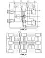
- the configurable logic IP module 102includes a system level configuration controller 104 . At least one standardized interconnect 108 such as AHB, OCP, and AXI is communicatively coupled to the system level configuration controller 104 .
- the configurable module 102may include at least one standardized configuration port 106 such as a JTAG port for programming the configurable module 102 .
- An embedded programmable logic fabric 118communicatively coupled to the system level configuration controller 104 and the standardized interconnect 108 , may be used for mapping arithmetic functions into standard cells.
- the configurable module 102may include at least one scalable configurable logic module (CLM) 112 , which may include a control block (CB) and 16 logic elements (LEs).
- FIG. 3shows an exemplary embodiment of the CLM 112
- FIG. 4is a table illustrating an exemplary 5 bit Arithmetic Logic Unit (ALU) of a logic element. An exemplary logic element is shown in FIG. 5 .
- ALUArithmetic Logic Unit
- the configurable module 102may include a memory 110 , an adder and/or multiplier on R-cell 114 , and a programmable routing matrix (not shown in FIG. 1 , but see FIG. 6 for an exemplary programmable routing matrix).
- FIGS. 7A and 7Bshow an exemplary switch box.
- the system level configuration controller 104may be suitable for selecting a standard for the at least one standardized interconnect 108 , the at least one standardized configuration port 106 , and a number of embedded programmable logic functions, and for controlling the programmable routing matrix.
- the configurable module 102may include a co-processor interface 120 , an on-chip IP bus 122 , and an IP bus 124 for connecting the configurable module 102 to the outside.
- FIG. 2shows an application specific configurable logic IP module (configurable module) 202 in accordance with an additional exemplary embodiment of the present invention.
- the configurable module 202may include a system level microcontroller 204 ; a JTAG port 206 ; standardized interconnects such as AHB, AXI, OCP 208 ; memory from RC slice, multiply divide unit, adder 210 ; and a scalable array of CL modules and scalable routing matrix 212 .
- FIG. 8is a flowchart of an ASIC design flow 800 .
- a specification of an integrated circuit productis received 802 .
- the specificationmay include information such as the application type, application features, target market, technology used, performance expected, embedded IP.
- Hardware and software partitionis implemented based on the specification 804 .
- the product and the addressed featuresneed to be implemented by software or implemented into hardware. Based on the application specific requirements and the product requirement, it is decided which needs to go into hardware.
- ASIC partitionis implemented based on the architecture of hardware to obtain ASIC elements and non-ASIC elements 808 .
- the cores (IP)are selected, and memories are sized. Considerable effort need be applied to seamlessly mapping all of the nonrandom logic elements within the ASIC.
- a RTL design for the ASICis implemented 810 .
- Functional verification of the RTL designis performed 812 .
- Logic synthesis and static timing analysis (STA)are performed 814 .
- the logic synthesisis a technology specific implementation of a function described in RTL (Verilog/VHDL).
- the STAdescribes a method to analyze (static mode) the timing response of the implemented function (output from the synthesis step). It is the main method to perform timing verification.
- Timing verificationis performed 816 .
- Product testis performed 818 , and test verification is implemented 820 .
- Initial placementis performed 822 , and final layout is implemented 824 .
- CL-IPConfigurable Logic IP
- the CL-IPincludes three main structural parts: the configuration part, the functional part and the interface part. Only the functional part is customizable. The configuration part and the interface part are pre-defined by the CL-IP module definition itself. From a customer perspective, the functional part of the CL-IP looks similar to the customer RTL. However, the target libraries of the implementation may differ.
- the process of developing a CL-IP module alongside the development of the ASIC-based end-productrequires careful planning at each stage of the flow. For example, after the system has been partitioned into ASIC and non-ASIC elements and after the cores have been selected and memories have been sized, considerable effort need be applied to seamlessly mapping all of the logic elements within the ASIC into a CL-IP module.
- RTLmay be designed such that by specifying parameters at compile time, it either represents an ASIC or a CL-IP module realization.
- the design databasemay be articulated via “branching” so that an ASIC and a CL-IP module of some design entities may coexist in the same database and the design may be built with one or another branch, depending on whether an ASIC or CL-IP module realization is desired.
- FIG. 9is a flowchart of a method 900 for integrating a configurable logic IP module into an ASIC design flow in accordance with an exemplary embodiment of the present invention.
- the steps 802 through 824are the same as those shown in FIG. 8 .
- a specific specification for the configurable logic IP modulemay be provided 930 .
- issuessuch as cores versus custom logic, memory sizing, etc. are resolved, and a complete specification is drafted, three efforts may begin in earnest in parallel: RTL design, test plan and verification environment development, and specifying the deviations to the ASIC RTL design in order to build a derivative with CL-IP.
- Integration of the configurable logic IP modulemay be implemented 932 .
- the step 930which focuses on the specification of the CL-IP modules
- the actual integrationmay be implemented at the step 932 .
- the top-level ASIC RTL instancemay include the ASIC, the CL-IP, the I/Os and the connection among each module. Based on the hierarchy level of the CL-IP module, the module interconnect to the rest of the ASIC and to the I/O ports as well as the interconnect to the JTAG module need to be implemented.
- RTL enhancements for the configurable logic IP modulemay be implemented to obtain a configurable logic IP RTL 934 .
- the ASIC RTLis well underway (if starting too soon, the job of keeping the ASIC and prototype in sync may prove too daunting)
- the deviations to the ASIC RTL described abovemay be implemented.
- the extent of the deviationsmay be kept to a bare minimum.
- both ASIC and CL-IP RTLmay reside in the same source. Thus, when bugs are uncovered downstream they need only be fixed in one place (and the odds that the prototype and the ASIC are functionally equivalent are greater). Since formal RTL to RTL equivalence checking is currently not viable, it is important that a major part of the RTL need be shared by both the ASIC and CL-IP module.
- Synthesis and layout for the configurable logic IP moduleare implemented 936 . Up until RTL is completed, the ASIC and FPGA design flows are more or less equivalent. Verilog or VHDL are suitable RTL languages for both. Assuming a no-nonsense coding style is employed, the same RTL may serve equally well for both. CL-IP may operate “near” speed (e.g., half-speed). The methodology of partitioning, synthesizing and layout for an ASIC versus a matrix of CL-IP is similar. The transistor level target library for the synthesis and the layout for the CL-IP may be the same as those for the ASIC logic.
- the CL-IPmay be mapped onto a couple of mega-functions such as a 4 Look-Up Table (LUT)-based architecture, which is commonly known by FPGA synthesis and layout tools. This may ensure the reconfigurable function of the CL-IP. Once the customer has specified the configurable part of the CL-IP, all other pre-defined building blocks may come along with it.
- LUTLook-Up Table
- the configurable logic IP moduleis built and debugged 938 .
- the mechanics of how to build and debug a CL-IPis interesting as well as when to do so.
- CL-IPmay be built out of ASIC RTL as soon as it is successfully compiled for the first time, it is preferred not to do so (except perhaps to verify that the CL-IP matrix can hold the RTL).
- a means of regressing both the ASIC and the CL-IPneed be established to ensure that the CL-IP and the ASIC represent the same thing.
- Debug in the lab on real hardwaremay be hard enough. A kind of hardware debug features is desirable.
- the configurable logic IP modulemay be released to software development 940 .
- CL-IPis a “soft” configurable solution, in which the logic elements are synthesizable and customizable.
- the IP and infrastructuremay be described in Verilog/VHDL RTL.
- Conventional methodsare “hardware” solutions on a physical layer and do not offer customization of the configurability.
- CL-IPmay also offer configurability on a system level.
- the CL-EPmay be implemented with the existing ASIC and RC design tools and may fit seamlessly into the existing design flows.
- the CL-IPmay be instantiated into RC and ASIC similar to a Landing Zone Processor.
- the present inventionmay provide a complete solution to the customer: from a Rapid Prototype device type, to a RapidChip with field programmable CL-IP, to a RapidChip with mask programmability, and to a standard cell ASIC solution.
- Such a software packagemay be a computer program product which employs a computer-readable storage medium including stored computer code which is used to program a computer to perform the disclosed function and process of the present invention.
- the computer-readable mediummay include, but is not limited to, any type of conventional floppy disk, optical disk, CD-ROM, magneto-optical disk, ROM, RAM, EPROM, EEPROM, magnetic or optical card, or any other suitable media for storing electronic instructions.
Landscapes
- Engineering & Computer Science (AREA)
- Computer Hardware Design (AREA)
- Physics & Mathematics (AREA)
- Theoretical Computer Science (AREA)
- Evolutionary Computation (AREA)
- Geometry (AREA)
- General Engineering & Computer Science (AREA)
- General Physics & Mathematics (AREA)
- Design And Manufacture Of Integrated Circuits (AREA)
Abstract
Description
Claims (16)
Priority Applications (1)
| Application Number | Priority Date | Filing Date | Title |
|---|---|---|---|
| US11/176,514US7451426B2 (en) | 2005-07-07 | 2005-07-07 | Application specific configurable logic IP |
Applications Claiming Priority (1)
| Application Number | Priority Date | Filing Date | Title |
|---|---|---|---|
| US11/176,514US7451426B2 (en) | 2005-07-07 | 2005-07-07 | Application specific configurable logic IP |
Publications (2)
| Publication Number | Publication Date |
|---|---|
| US20070011642A1 US20070011642A1 (en) | 2007-01-11 |
| US7451426B2true US7451426B2 (en) | 2008-11-11 |
Family
ID=37619684
Family Applications (1)
| Application Number | Title | Priority Date | Filing Date |
|---|---|---|---|
| US11/176,514Expired - Fee RelatedUS7451426B2 (en) | 2005-07-07 | 2005-07-07 | Application specific configurable logic IP |
Country Status (1)
| Country | Link |
|---|---|
| US (1) | US7451426B2 (en) |
Cited By (9)
| Publication number | Priority date | Publication date | Assignee | Title |
|---|---|---|---|---|
| US20070294658A1 (en)* | 2006-06-15 | 2007-12-20 | National Chip Implementation Center | Multi-project system-on-chip and its method |
| US9293450B2 (en)* | 2014-07-22 | 2016-03-22 | Freescale Semiconductor, Inc. | Synthesis of complex cells |
| US11074380B2 (en) | 2016-09-29 | 2021-07-27 | Amazon Technologies, Inc. | Logic repository service |
| US11099894B2 (en) | 2016-09-28 | 2021-08-24 | Amazon Technologies, Inc. | Intermediate host integrated circuit between virtual machine instance and customer programmable logic |
| US11115293B2 (en) | 2016-11-17 | 2021-09-07 | Amazon Technologies, Inc. | Networked programmable logic service provider |
| US11119150B2 (en) | 2016-09-28 | 2021-09-14 | Amazon Technologies, Inc. | Extracting debug information from FPGAs in multi-tenant environments |
| US11171933B2 (en) | 2016-09-29 | 2021-11-09 | Amazon Technologies, Inc. | Logic repository service using encrypted configuration data |
| US11182320B2 (en)* | 2016-09-29 | 2021-11-23 | Amazon Technologies, Inc. | Configurable logic platform with multiple reconfigurable regions |
| US11275503B2 (en) | 2016-09-30 | 2022-03-15 | Amazon Technologies, Inc. | Controlling access to previously-stored logic in a reconfigurable logic device |
Families Citing this family (4)
| Publication number | Priority date | Publication date | Assignee | Title |
|---|---|---|---|---|
| FR2972566B1 (en)* | 2011-03-11 | 2013-03-15 | Sas Adicsys Design | MONO-CHIP SYSTEM COMPRISING A SYNTHETICABLE PROGRAMMABLE HEART AND A METHOD OF MANUFACTURING SUCH A SYSTEM |
| US8677306B1 (en)* | 2012-10-11 | 2014-03-18 | Easic Corporation | Microcontroller controlled or direct mode controlled network-fabric on a structured ASIC |
| US20220044123A1 (en)* | 2021-09-24 | 2022-02-10 | Rajesh Vivekanandham | Embedded Programmable Logic Device for Acceleration in Deep Learning-Focused Processors |
| CN118246373B (en)* | 2024-03-19 | 2024-12-13 | 无锡众星微系统技术有限公司 | A software and hardware handshake method and device for switching chip working mode |
Citations (19)
| Publication number | Priority date | Publication date | Assignee | Title |
|---|---|---|---|---|
| US6567957B1 (en)* | 1998-09-30 | 2003-05-20 | Cadence Design Systems, Inc. | Block based design methodology |
| US6732354B2 (en)* | 2002-04-23 | 2004-05-04 | Quicksilver Technology, Inc. | Method, system and software for programming reconfigurable hardware |
| US20040141518A1 (en)* | 2003-01-22 | 2004-07-22 | Alison Milligan | Flexible multimode chip design for storage and networking |
| US6785876B2 (en)* | 2000-11-16 | 2004-08-31 | Matsushita Electric Industrial Co., Ltd. | Design method for semiconductor integrated circuit device |
| US20050010378A1 (en)* | 2003-06-27 | 2005-01-13 | Zeidman Technologies, Inc. | Method and apparatus for synthesizing a hardware system from a software description |
| US20050023656A1 (en)* | 2002-08-08 | 2005-02-03 | Leedy Glenn J. | Vertical system integration |
| US20050165995A1 (en)* | 2001-03-15 | 2005-07-28 | Italtel S.P.A. | System of distributed microprocessor interfaces toward macro-cell based designs implemented as ASIC or FPGA bread boarding and relative COMMON BUS protocol |
| US20050229143A1 (en)* | 2004-04-01 | 2005-10-13 | Lsi Logic Corporation | System and method for implementing multiple instantiated configurable peripherals in a circuit design |
| US6959428B2 (en)* | 2003-06-19 | 2005-10-25 | Lsi Logic Corporation | Designing and testing the interconnection of addressable devices of integrated circuits |
| US7012448B2 (en)* | 2001-04-07 | 2006-03-14 | The University Court Of The University Of Dundee | Integrated circuit and related improvements |
| US7051309B1 (en)* | 1999-02-16 | 2006-05-23 | Crosetto Dario B | Implementation of fast data processing with mixed-signal and purely digital 3D-flow processing boars |
| US7072818B1 (en)* | 1999-11-30 | 2006-07-04 | Synplicity, Inc. | Method and system for debugging an electronic system |
| US20060236292A1 (en)* | 2005-03-14 | 2006-10-19 | Lsi Logic Corporation | Base platforms with combined ASIC and FPGA features and process of using the same |
| US7131098B2 (en)* | 2003-11-17 | 2006-10-31 | International Business Machines Corporation | Computer program product for implementing uncertainty in integrated circuit designs with programmable logic |
| US7200703B2 (en)* | 2004-06-08 | 2007-04-03 | Valmiki Ramanujan K | Configurable components for embedded system design |
| US7212961B2 (en)* | 2002-08-30 | 2007-05-01 | Lsi Logic Corporation | Interface for rapid prototyping system |
| US7237214B1 (en)* | 2003-03-04 | 2007-06-26 | Synplicity, Inc. | Method and apparatus for circuit partitioning and trace assignment in circuit design |
| US7240303B1 (en)* | 1999-11-30 | 2007-07-03 | Synplicity, Inc. | Hardware/software co-debugging in a hardware description language |
| US7290224B2 (en)* | 2004-06-03 | 2007-10-30 | Lsi Corporation | Guided capture, creation, and seamless integration with scalable complexity of a clock specification into a design flow of an integrated circuit |
- 2005
- 2005-07-07USUS11/176,514patent/US7451426B2/ennot_activeExpired - Fee Related
Patent Citations (19)
| Publication number | Priority date | Publication date | Assignee | Title |
|---|---|---|---|---|
| US6567957B1 (en)* | 1998-09-30 | 2003-05-20 | Cadence Design Systems, Inc. | Block based design methodology |
| US7051309B1 (en)* | 1999-02-16 | 2006-05-23 | Crosetto Dario B | Implementation of fast data processing with mixed-signal and purely digital 3D-flow processing boars |
| US7240303B1 (en)* | 1999-11-30 | 2007-07-03 | Synplicity, Inc. | Hardware/software co-debugging in a hardware description language |
| US7072818B1 (en)* | 1999-11-30 | 2006-07-04 | Synplicity, Inc. | Method and system for debugging an electronic system |
| US6785876B2 (en)* | 2000-11-16 | 2004-08-31 | Matsushita Electric Industrial Co., Ltd. | Design method for semiconductor integrated circuit device |
| US20050165995A1 (en)* | 2001-03-15 | 2005-07-28 | Italtel S.P.A. | System of distributed microprocessor interfaces toward macro-cell based designs implemented as ASIC or FPGA bread boarding and relative COMMON BUS protocol |
| US7012448B2 (en)* | 2001-04-07 | 2006-03-14 | The University Court Of The University Of Dundee | Integrated circuit and related improvements |
| US6732354B2 (en)* | 2002-04-23 | 2004-05-04 | Quicksilver Technology, Inc. | Method, system and software for programming reconfigurable hardware |
| US20050023656A1 (en)* | 2002-08-08 | 2005-02-03 | Leedy Glenn J. | Vertical system integration |
| US7212961B2 (en)* | 2002-08-30 | 2007-05-01 | Lsi Logic Corporation | Interface for rapid prototyping system |
| US20040141518A1 (en)* | 2003-01-22 | 2004-07-22 | Alison Milligan | Flexible multimode chip design for storage and networking |
| US7237214B1 (en)* | 2003-03-04 | 2007-06-26 | Synplicity, Inc. | Method and apparatus for circuit partitioning and trace assignment in circuit design |
| US6959428B2 (en)* | 2003-06-19 | 2005-10-25 | Lsi Logic Corporation | Designing and testing the interconnection of addressable devices of integrated circuits |
| US20050010378A1 (en)* | 2003-06-27 | 2005-01-13 | Zeidman Technologies, Inc. | Method and apparatus for synthesizing a hardware system from a software description |
| US7131098B2 (en)* | 2003-11-17 | 2006-10-31 | International Business Machines Corporation | Computer program product for implementing uncertainty in integrated circuit designs with programmable logic |
| US20050229143A1 (en)* | 2004-04-01 | 2005-10-13 | Lsi Logic Corporation | System and method for implementing multiple instantiated configurable peripherals in a circuit design |
| US7290224B2 (en)* | 2004-06-03 | 2007-10-30 | Lsi Corporation | Guided capture, creation, and seamless integration with scalable complexity of a clock specification into a design flow of an integrated circuit |
| US7200703B2 (en)* | 2004-06-08 | 2007-04-03 | Valmiki Ramanujan K | Configurable components for embedded system design |
| US20060236292A1 (en)* | 2005-03-14 | 2006-10-19 | Lsi Logic Corporation | Base platforms with combined ASIC and FPGA features and process of using the same |
Non-Patent Citations (1)
| Title |
|---|
| Garp: A MIPS Processor with a Reconfigurable Coprocessor; John R. Hauser and John Wawrzynek, University of California, Berkley. |
Cited By (10)
| Publication number | Priority date | Publication date | Assignee | Title |
|---|---|---|---|---|
| US20070294658A1 (en)* | 2006-06-15 | 2007-12-20 | National Chip Implementation Center | Multi-project system-on-chip and its method |
| US7571414B2 (en)* | 2006-06-15 | 2009-08-04 | National Chip Implementation Center, National Applied Research Laboratories | Multi-project system-on-chip and its method |
| US9293450B2 (en)* | 2014-07-22 | 2016-03-22 | Freescale Semiconductor, Inc. | Synthesis of complex cells |
| US11099894B2 (en) | 2016-09-28 | 2021-08-24 | Amazon Technologies, Inc. | Intermediate host integrated circuit between virtual machine instance and customer programmable logic |
| US11119150B2 (en) | 2016-09-28 | 2021-09-14 | Amazon Technologies, Inc. | Extracting debug information from FPGAs in multi-tenant environments |
| US11074380B2 (en) | 2016-09-29 | 2021-07-27 | Amazon Technologies, Inc. | Logic repository service |
| US11171933B2 (en) | 2016-09-29 | 2021-11-09 | Amazon Technologies, Inc. | Logic repository service using encrypted configuration data |
| US11182320B2 (en)* | 2016-09-29 | 2021-11-23 | Amazon Technologies, Inc. | Configurable logic platform with multiple reconfigurable regions |
| US11275503B2 (en) | 2016-09-30 | 2022-03-15 | Amazon Technologies, Inc. | Controlling access to previously-stored logic in a reconfigurable logic device |
| US11115293B2 (en) | 2016-11-17 | 2021-09-07 | Amazon Technologies, Inc. | Networked programmable logic service provider |
Also Published As
| Publication number | Publication date |
|---|---|
| US20070011642A1 (en) | 2007-01-11 |
Similar Documents
| Publication | Publication Date | Title |
|---|---|---|
| US7627848B2 (en) | Bit stream compatible FPGA to MPGA conversions | |
| Saleh et al. | System-on-chip: Reuse and integration | |
| Wilton et al. | Programmable logic IP cores in SoC design: Opportunities and challenges | |
| Claasen | An industry perspective on current and future state of the art in system-on-chip (SoC) technology | |
| US7451426B2 (en) | Application specific configurable logic IP | |
| US7032191B2 (en) | Method and architecture for integrated circuit design and manufacture | |
| Darringer et al. | EDA in IBM: past, present, and future | |
| US8037432B2 (en) | Method and apparatus for mapping design memories to integrated circuit layout | |
| US8910103B2 (en) | Method of designing a high performance application specific integrated circuit accelerator | |
| Thuries et al. | M3D-ADTCO: Monolithic 3D architecture, design and technology co-optimization for high energy efficient 3D IC | |
| TWI853294B (en) | Integrated circuits and methods for integrated circuit design and manufacture | |
| US6581200B2 (en) | Abstracting netlist to manage routing information | |
| Chakravarthi et al. | Introduction to design of system on chips and future trends in VLSI | |
| Dutt et al. | Design synthesis and silicon compilation | |
| Veendrick | Very-Large-Scale Integration (VLSI) and ASICs | |
| Newton et al. | CAD tools for ASIC design | |
| Huang et al. | Programmable system-on-chip for silicon prototyping | |
| Puri et al. | The dawn of 22nm era: Design and CAD challenges | |
| Dunlop et al. | Managing complexity in IC design—past, present, and future | |
| Fox | A higher level of synthesis (CAD) | |
| US7491579B2 (en) | Composable system-in-package integrated circuits and process of composing the same | |
| US20070108961A1 (en) | Method and apparatus for tiling memories in integrated circuit layout | |
| Baek et al. | Selectively patterned masks: Structured ASIC with asymptotically ASIC performance | |
| Barkalov et al. | Design of Embedded Systems | |
| Vaida | PLC advanced technology demonstrator testchipb |
Legal Events
| Date | Code | Title | Description |
|---|---|---|---|
| AS | Assignment | Owner name:LSI LOGIC CORPORATION, CALIFORNIA Free format text:ASSIGNMENT OF ASSIGNORS INTEREST;ASSIGNOR:PRIBBERNOW, CLAUS;REEL/FRAME:016770/0314 Effective date:20050707 | |
| AS | Assignment | Owner name:LSI CORPORATION, CALIFORNIA Free format text:MERGER;ASSIGNOR:LSI SUBSIDIARY CORP.;REEL/FRAME:020548/0977 Effective date:20070404 Owner name:LSI CORPORATION,CALIFORNIA Free format text:MERGER;ASSIGNOR:LSI SUBSIDIARY CORP.;REEL/FRAME:020548/0977 Effective date:20070404 | |
| FEPP | Fee payment procedure | Free format text:PAYOR NUMBER ASSIGNED (ORIGINAL EVENT CODE: ASPN); ENTITY STATUS OF PATENT OWNER: LARGE ENTITY | |
| FPAY | Fee payment | Year of fee payment:4 | |
| AS | Assignment | Owner name:DEUTSCHE BANK AG NEW YORK BRANCH, AS COLLATERAL AG Free format text:PATENT SECURITY AGREEMENT;ASSIGNORS:LSI CORPORATION;AGERE SYSTEMS LLC;REEL/FRAME:032856/0031 Effective date:20140506 | |
| AS | Assignment | Owner name:LSI CORPORATION, CALIFORNIA Free format text:CHANGE OF NAME;ASSIGNOR:LSI LOGIC CORPORATION;REEL/FRAME:033102/0270 Effective date:20070406 | |
| AS | Assignment | Owner name:AVAGO TECHNOLOGIES GENERAL IP (SINGAPORE) PTE. LTD Free format text:ASSIGNMENT OF ASSIGNORS INTEREST;ASSIGNOR:LSI CORPORATION;REEL/FRAME:035390/0388 Effective date:20140814 | |
| AS | Assignment | Owner name:AGERE SYSTEMS LLC, PENNSYLVANIA Free format text:TERMINATION AND RELEASE OF SECURITY INTEREST IN PATENT RIGHTS (RELEASES RF 032856-0031);ASSIGNOR:DEUTSCHE BANK AG NEW YORK BRANCH, AS COLLATERAL AGENT;REEL/FRAME:037684/0039 Effective date:20160201 Owner name:LSI CORPORATION, CALIFORNIA Free format text:TERMINATION AND RELEASE OF SECURITY INTEREST IN PATENT RIGHTS (RELEASES RF 032856-0031);ASSIGNOR:DEUTSCHE BANK AG NEW YORK BRANCH, AS COLLATERAL AGENT;REEL/FRAME:037684/0039 Effective date:20160201 | |
| AS | Assignment | Owner name:BANK OF AMERICA, N.A., AS COLLATERAL AGENT, NORTH CAROLINA Free format text:PATENT SECURITY AGREEMENT;ASSIGNOR:AVAGO TECHNOLOGIES GENERAL IP (SINGAPORE) PTE. LTD.;REEL/FRAME:037808/0001 Effective date:20160201 Owner name:BANK OF AMERICA, N.A., AS COLLATERAL AGENT, NORTH Free format text:PATENT SECURITY AGREEMENT;ASSIGNOR:AVAGO TECHNOLOGIES GENERAL IP (SINGAPORE) PTE. LTD.;REEL/FRAME:037808/0001 Effective date:20160201 | |
| REMI | Maintenance fee reminder mailed | ||
| LAPS | Lapse for failure to pay maintenance fees | ||
| STCH | Information on status: patent discontinuation | Free format text:PATENT EXPIRED DUE TO NONPAYMENT OF MAINTENANCE FEES UNDER 37 CFR 1.362 | |
| FP | Lapsed due to failure to pay maintenance fee | Effective date:20161111 | |
| AS | Assignment | Owner name:AVAGO TECHNOLOGIES GENERAL IP (SINGAPORE) PTE. LTD., SINGAPORE Free format text:TERMINATION AND RELEASE OF SECURITY INTEREST IN PATENTS;ASSIGNOR:BANK OF AMERICA, N.A., AS COLLATERAL AGENT;REEL/FRAME:041710/0001 Effective date:20170119 Owner name:AVAGO TECHNOLOGIES GENERAL IP (SINGAPORE) PTE. LTD Free format text:TERMINATION AND RELEASE OF SECURITY INTEREST IN PATENTS;ASSIGNOR:BANK OF AMERICA, N.A., AS COLLATERAL AGENT;REEL/FRAME:041710/0001 Effective date:20170119 | |
| AS | Assignment | Owner name:BELL SEMICONDUCTOR, LLC, ILLINOIS Free format text:ASSIGNMENT OF ASSIGNORS INTEREST;ASSIGNORS:AVAGO TECHNOLOGIES GENERAL IP (SINGAPORE) PTE. LTD.;BROADCOM CORPORATION;REEL/FRAME:044887/0109 Effective date:20171208 | |
| AS | Assignment | Owner name:CORTLAND CAPITAL MARKET SERVICES LLC, AS COLLATERA Free format text:SECURITY INTEREST;ASSIGNORS:HILCO PATENT ACQUISITION 56, LLC;BELL SEMICONDUCTOR, LLC;BELL NORTHERN RESEARCH, LLC;REEL/FRAME:045216/0020 Effective date:20180124 | |
| AS | Assignment | Owner name:BELL NORTHERN RESEARCH, LLC, ILLINOIS Free format text:RELEASE BY SECURED PARTY;ASSIGNOR:CORTLAND CAPITAL MARKET SERVICES LLC;REEL/FRAME:059720/0223 Effective date:20220401 Owner name:BELL SEMICONDUCTOR, LLC, ILLINOIS Free format text:RELEASE BY SECURED PARTY;ASSIGNOR:CORTLAND CAPITAL MARKET SERVICES LLC;REEL/FRAME:059720/0223 Effective date:20220401 Owner name:HILCO PATENT ACQUISITION 56, LLC, ILLINOIS Free format text:RELEASE BY SECURED PARTY;ASSIGNOR:CORTLAND CAPITAL MARKET SERVICES LLC;REEL/FRAME:059720/0223 Effective date:20220401 |