US7451273B2 - System, method and storage medium for providing data caching and data compression in a memory subsystem - Google Patents
System, method and storage medium for providing data caching and data compression in a memory subsystemDownload PDFInfo
- Publication number
- US7451273B2 US7451273B2US11/780,048US78004807AUS7451273B2US 7451273 B2US7451273 B2US 7451273B2US 78004807 AUS78004807 AUS 78004807AUS 7451273 B2US7451273 B2US 7451273B2
- Authority
- US
- United States
- Prior art keywords
- memory
- data
- cache
- bus
- module
- Prior art date
- Legal status (The legal status is an assumption and is not a legal conclusion. Google has not performed a legal analysis and makes no representation as to the accuracy of the status listed.)
- Expired - Fee Related
Links
Images


Classifications
- G—PHYSICS
- G06—COMPUTING OR CALCULATING; COUNTING
- G06F—ELECTRIC DIGITAL DATA PROCESSING
- G06F13/00—Interconnection of, or transfer of information or other signals between, memories, input/output devices or central processing units
- G06F13/14—Handling requests for interconnection or transfer
- G06F13/16—Handling requests for interconnection or transfer for access to memory bus
- G06F13/1668—Details of memory controller
- G06F13/1684—Details of memory controller using multiple buses
- G—PHYSICS
- G06—COMPUTING OR CALCULATING; COUNTING
- G06F—ELECTRIC DIGITAL DATA PROCESSING
- G06F12/00—Accessing, addressing or allocating within memory systems or architectures
- G06F12/02—Addressing or allocation; Relocation
- G06F12/08—Addressing or allocation; Relocation in hierarchically structured memory systems, e.g. virtual memory systems
- G06F12/0802—Addressing of a memory level in which the access to the desired data or data block requires associative addressing means, e.g. caches
- G—PHYSICS
- G06—COMPUTING OR CALCULATING; COUNTING
- G06F—ELECTRIC DIGITAL DATA PROCESSING
- G06F2212/00—Indexing scheme relating to accessing, addressing or allocation within memory systems or architectures
- G06F2212/40—Specific encoding of data in memory or cache
- G06F2212/401—Compressed data
Definitions
- the inventionrelates to a memory subsystem and, in particular, to providing data caching and data compression in a memory subsystem.
- Computer memory subsystemshave evolved over the years, but continue to retain many consistent attributes.
- Computer memory subsystems from the early 1980'ssuch as the one disclosed in U.S. Pat. No. 4,475,194 to LaVallee et al., of common assignment herewith, included a memory controller, a memory assembly (contemporarily called a basic storage module (BSM) by the inventors) with array devices, buffers, terminators and ancillary timing and control functions, as well as several point-to-point busses to permit each memory assembly to communicate with the memory controller via its own point-to-point address and data bus.
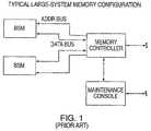
- FIG. 1depicts an example of this early 1980 computer memory subsystem with two BSMs, a memory controller, a maintenance console, and point-to-point address and data busses connecting the BSMs and the memory controller.
- FIG. 2from U.S. Pat. No. 5,513,135 to Dell et al., of common assignment herewith, depicts an early synchronous memory module, which includes synchronous dynamic random access memories (DRAMs) 8 , buffer devices 12 , an optimized pinout, an interconnect and a capacitive decoupling method to facilitate operation.
- DRAMssynchronous dynamic random access memories
- PLLsphase lock loops
- FIG. 3depicts a simplified diagram and description of a memory system 10 that includes up to four registered dual inline memory modules (DIMMs) 40 on a traditional multi-drop stub bus channel.
- the subsystemincludes a memory controller 20 , an external clock buffer 30 , registered DIMMs 40 , an address bus 50 , a control bus 60 and a data bus 70 with terminators 95 on the address bus 50 and data bus 70 .
- FIG. 4depicts a 1990's memory subsystem which evolved from the structure in FIG. 1 and includes a memory controller 402 , one or more high speed point-to-point channels 404 , each connected to a bus-to-bus converter chip 406 , and each having a synchronous memory interface 408 that enables connection to one or more registered DIMMs 410 .
- the high speed, point-to-point channel 404operated at twice the DRAM data rate, allowing the bus-to-bus converter chip 406 to operate one or two registered DIMM memory channels at the full DRAM data rate.
- Each registered DIMMincluded a PLL, registers, DRAMs, an electrically erasable programmable read-only memory (EEPROM) and terminators, in addition to other passive components.
- EEPROMelectrically erasable programmable read-only memory
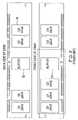
- FIG. 5is a simplified example of a multi-drop stub bus memory structure, similar to the one shown in FIG. 3 .
- This structureoffers a reasonable tradeoff between cost, performance, reliability and upgrade capability, but has inherent limits on the number of modules that may be attached to the stub bus.
- the limit on the number of modules that may be attached to the stub busis directly related to the data rate of the information transferred over the bus. As data rates increase, the number and length of the stubs must be reduced to ensure robust memory operation.
- Increasing the speed of the busgenerally results in a reduction in modules on the bus with the optimal electrical interface being one in which a single module is directly connected to a single controller, or a point-to-point interface with few, if any, stubs that will result in reflections and impedance discontinuities.
- the optimal electrical interfacebeing one in which a single module is directly connected to a single controller, or a point-to-point interface with few, if any, stubs that will result in reflections and impedance discontinuities.
- this structurealso requires a large number of pins to transfer address, command, and data.
- One hundred and twenty pinsare identified in FIG. 5 as being a representative pincount.
- FIG. 6from U.S. Pat. No. 4,723,120 to Petty, of common assignment herewith, is related to the application of a daisy chain structure in a multipoint communication structure that would otherwise require multiple ports, each connected via point-to-point interfaces to separate devices.
- the controlling stationcan be produced with fewer ports (or channels), and each device on the channel can utilize standard upstream and downstream protocols, independent of their location in the daisy chain structure.
- FIG. 7represents a daisy chained memory bus, implemented consistent with the teachings in U.S. Pat. No. 4,723,120.
- a memory controller 111is connected to a memory bus 315 , which further connects to a module 310 a .
- the information on bus 315is re-driven by the buffer on module 310 a to a next module, 310 b , which further re-drives the bus 315 to module positions denoted as 310 n .
- Each module 310 aincludes a DRAM 311 a and a buffer 320 a .
- the bus 315may be described as having a daisy chain structure with each bus being point-to-point in nature.
- One drawback to the use of a daisy chain busis associated with providing enhanced capabilities such as data caching and data compression. Adding enhanced capabilities may result in an indeterminate read data latency because the amount of time required to read a particular item of data cannot be pre-determined by the memory controller. The read latency will depend on several varying factors such as whether the data is located in a cache and whether the data has to be decompressed before being returned to the memory controller.
- the ability to add data caching and/or data compression in a pluggable fashion to selected modules in a daisy chain busis desirable because these enhanced capabilities may lead to improved performance and space savings within a memory subsystem.
- Exemplary embodiments of the present inventioninclude a cascaded interconnect system including a memory controller, one or more memory modules, an upstream memory bus and a downstream memory bus.
- the one or more memory modulesinclude a first memory module with cache data.
- the memory modules and the memory controllerare interconnected by a packetized multi-transfer interface via the downstream memory bus and the upstream memory bus.
- the first memory module and the memory controllerare in direct communication via the upstream memory bus and the downstream memory bus.
- Another exemplary embodiment of the present inventionincludes a memory controller, one or more memory modules, an upstream memory bus and a downstream memory bus.
- the one or more memory moduleseach include memory modules a plurality of corresponding memory devices. At least one of the memory modules includes cache data sourced from the corresponding memory devices on the memory module and a cache directory corresponding to the cache data.
- the memory modules and the memory controllerare interconnected by a packetized multi-transfer interface via the downstream memory bus and the upstream memory bus.
- the memory controllerutilizes a read data tag on data read requests sent via the downstream memory bus and the read data tag on data return results received via the upstream memory bus to match the data read requests with the data return results.
- Another exemplary embodiment of the present inventionincludes a memory controller, one or more memory modules, an upstream memory bus and a downstream memory bus.
- the one or more memory modulesinclude a first memory module with a data compression module for compressing and decompressing data stored on the memory modules.
- the memory modules and the memory controllerare interconnected by a packetized multi-transfer interface via the downstream memory bus and the upstream memory bus.
- the first memory module and the memory controllerare in direct communication via the upstream memory bus and the downstream memory bus.
- a further exemplary embodiment of the present inventionincludes a cascaded interconnect system with a memory controller, one or more memory modules, an upstream memory bus and a downstream memory bus.
- the one or more memory moduleseach include a plurality of corresponding memory devices and at least one of the memory modules includes a data compression module.
- the memory modules and the memory controllerare interconnected by a packetized multi-transfer interface via the downstream memory bus and the upstream memory bus.
- the memory controllerutilizes a read data tag on data read requests sent via the downstream memory bus and the read data tag on data return results received via the upstream memory bus to match the data read requests with the data return results.
- a further exemplary embodiment of the present inventionincludes a method for providing data caching in a memory system.
- the methodincludes receiving a request at a selected memory module to read data at a specified data address.
- the requestis from a memory controller in a cascaded memory system and the selected memory module is one of one or more memory modules included in the cascaded memory system.
- a cache directoryis searched for the data address.
- the datais read from cache data in response to locating the data address in the cache directory.
- the datais read from one of the memory devices in response to not locating the data address in the cache directory.
- the datais transmitted to the memory controller.
- a further exemplary embodiment of the present inventionincludes a method for providing data compression in a memory system.
- the methodincludes receiving a request at a selected memory module to read data at a specified data address.
- the requestcomes from a memory controller in a cascaded memory system and the selected memory module is one of one or more memory modules included in the cascaded memory system. It is determined if the data is compressed and the data is decompressed if it is determined to be compressed. The data is then transmitted to the memory controller.
- a further exemplary embodiment of the present inventionincludes a storage medium encoded with machine readable computer program code for providing data caching in a memory subsystem.
- the storage mediumincludes instructions for causing a computer to implement a method.
- the methodincludes receiving a request at a selected memory module to read data at a specified data address.
- the requestis from a memory controller in a cascaded memory system and the selected memory module is one of one or more memory modules included in the cascaded memory system.
- a cache directoryis searched for the data address.
- the datais read from cache data in response to locating the data address in the cache directory.
- the datais read from one of the memory devices in response to not locating the data address in the cache directory.
- the datais transmitted to the memory controller.
- a further exemplary embodiment of the present inventionincludes a storage medium encoded with machine readable computer program code for providing data compression in a memory subsystem.
- the storage mediumincludes instructions for causing a computer to implement a method.
- the methodincludes receiving a request at a selected memory module to read data at a specified data address.
- the requestcomes from a memory controller in a cascaded memory system and the selected memory module is one of one or more memory modules included in the cascaded memory system. It is determined if the data is compressed and the data is decompressed if it is determined to be compressed. The data is then transmitted to the memory controller.
- FIG. 1depicts a prior art memory controller connected to two buffered memory assemblies via separate point-to-point links;
- FIG. 2depicts a prior art synchronous memory module with a buffer device
- FIG. 3depicts a prior art memory subsystem using registered DIMMs
- FIG. 4depicts a prior art memory subsystem with point-to-point channels, registered DIMMs, and a 2:1 bus speed multiplier;
- FIG. 5depicts a prior art memory structure that utilizes a multidrop memory ‘stub’ bus
- FIG. 6depicts a prior art daisy chain structure in a multipoint communication structure that would otherwise require multiple ports
- FIG. 7depicts a prior art daisy chain connection between a memory controller and memory modules
- FIG. 8depicts a cascaded memory structure that is utilized by exemplary embodiments of the present invention.
- FIG. 9depicts a memory structure with cascaded memory modules and unidirectional busses that is utilized by exemplary embodiments of the present invention.
- FIG. 10depicts a buffered module wiring system that is utilized by exemplary embodiments of the present invention.
- FIG. 11depicts a memory structure with cached data that may be utilized by exemplary embodiments of the present invention.
- FIG. 12depicts a memory structure with cached data that may be utilized by exemplary embodiments of the present invention.
- FIG. 13depicts a memory structure with data compression that may be utilized by exemplary embodiments of the present invention.
- FIG. 14depicts a memory structure with cached data and data compression that may be utilized by exemplary embodiments of the present invention.
- Exemplary embodiments of the present inventionprovide an enhanced memory subsystem (or memory channel) by including data caching capability in one or more memory modules within a cascaded memory subsystem.
- the memory controllerhas access to a cache directory for the memory subsystem
- the deterministic nature of the controller interface protocol utilized by the memory subsystemis preserved.
- reads to the cache datacan be predetermined and specifically requested by the memory controller.
- the read data return from such reads to the cache datamay be scheduled using standard mechanisms.
- Additional embodiments of the present inventionprovide for a memory subsystem where the cache directory does not reside in the memory controller and is not accessible by the memory controller.
- the addition of cache to the memory subsystemresults in indeterminate read data latencies.
- a tag signalis added to the upstream controller interface frame format so that returned read data may be identified by the memory controller. This read data identification removes the requirement that the memory controller be able to predict the exact return time of each read request.
- the ability to handle indeterminate read data latencyallows the memory modules in the memory channel to utilize enhanced features (e.g., data caching and data compression) that modify the normally predictable read data return times.
- FIG. 8depicts a cascaded memory structure that may be utilized by exemplary embodiments of the present invention when buffered memory modules 806 (e.g., the buffer device is included within the memory module 806 ) are in communication with a memory controller 802 .
- This memory structureincludes the memory controller 802 in communication with one or more memory modules 806 via a high speed point-to-point bus 804 .
- Each bus 804 in the exemplary embodiment depicted in FIG. 8includes approximately fifty high speed wires for the transfer of address, command, data and clocks.
- FIG. 4depicts a memory subsystem with a two to one ratio between the data rate on any one of the busses connecting the memory controller to one of the bus converters (e.g., to 1,066 Mb/s per pin) versus any one of the busses between the bus converter and one or more memory modules (e.g., to 533 Mb/s per pin), an exemplary embodiment of the present invention, as depicted in FIG. 8 , provides a four to one bus speed ratio to maximize bus efficiency and to minimize pincount.
- point-to-point interconnectspermit higher data rates, overall memory subsystem efficiency must be achieved by maintaining a reasonable number of memory modules 806 and memory devices per channel (historically four memory modules with four to thirty-six chips per memory module, but as high as eight memory modules per channel and as few as one memory module per channel).
- Using a point-to-point busnecessitates a bus re-drive function on each memory module to permit memory modules to be cascaded such that each memory module is interconnected to other memory modules, as well as to the memory controller 802 .
- FIG. 9depicts a memory structure with cascaded memory modules and unidirectional busses that is utilized by exemplary embodiments of the present invention.
- One of the functions provided by the memory modules 806 in the cascade structureis a re-drive function to send signals on the memory bus to other memory modules 806 or to the memory controller 802 .
- FIG. 9includes the memory controller 802 and four memory modules 806 a , 806 b , 806 c and 806 d , on each of two memory busses (a downstream memory bus 904 and an upstream memory bus 902 ), connected to the memory controller 802 in either a direct or cascaded manner.
- Memory module 806 ais connected to the memory controller 802 in a direct manner.
- Memory modules 806 b , 806 c and 806 dare connected to the memory controller 802 in a cascaded manner.
- An exemplary embodiment of the present inventionincludes two uni-directional busses between the memory controller 802 and memory module 806 a (“DIMM # 1 ”), as well as between each successive memory module 806 b - d (“DIMM # 2 ”, “DIMM # 3 ” and “DIMM # 4 ”) in the cascaded memory structure.
- the downstream memory bus 904is comprised of twenty-two single-ended signals and a differential clock pair.
- the downstream memory bus 904is used to transfer address, control, write data and bus-level error code correction (ECC) bits downstream from the memory controller 802 , over several clock cycles, to one or more of the memory modules 806 installed on the cascaded memory channel.
- ECCbus-level error code correction
- the upstream memory bus 902is comprised of twenty-three single-ended signals and a differential clock pair, and is used to transfer read data and bus-level ECC bits upstream from the sourcing memory module 806 to the memory controller 802 . Because the upstream memory bus 902 and the downstream memory bus 904 are unidirectional and operate independently, read data, write data and memory commands may be transmitted simultaneously. This increases effective memory subsystem bandwidth and may result in higher system performance.
- the memory controller 802 signal pincount, per memory channelis reduced from approximately one hundred and twenty pins to about fifty pins.
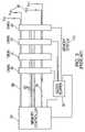
- FIG. 10depicts a buffered module wiring system that is utilized by exemplary embodiments of the present invention.
- FIG. 10is a pictorial representation of a memory module with shaded arrows representing the primary signal flows.
- the signal flowsinclude the upstream memory bus 902 , the downstream memory bus 904 , memory device address and command busses 1010 and 1006 , and memory device data busses 1012 and 1008 .
- a buffer device 1002also referred to as a memory interface chip, provides two copies of the address and command signals to the SDRAMs 1004 with the right memory device address and command bus 1006 exiting from the right side of the buffer device 1002 for the SDRAMs 1004 located to the right side and behind the buffer device 1002 on the right.
- the left memory device address and command bus 1010exits from the left side of the buffer device 1002 and connects to the SDRAMs 1004 to the left side and behind the buffer device 1002 on the left.
- the data bits intended for SDRAMs 1004 to the right of the buffer device 1002exit from the right of the buffer device 1002 on the right memory device data bus 1008 .
- the data bits intended for the left side of the buffer device 1002exit from the left of the buffer device 1002 on the left memory device data bus 1012 .
- the high speed upstream memory bus 902 and downstream memory bus 904exit from the lower portion of the buffer device 1002 , and connect to a memory controller or other memory modules either upstream or downstream of this memory module 806 , depending on the application.
- the buffer device 1002receives signals that are four times the memory module data rate and converts them into signals at the memory module data rate.
- the memory controller 802interfaces to the memory modules 806 via a pair of high speed busses (or channels).
- the downstream memory bus 904 (outbound from the memory controller 802 ) interfacehas twenty-four pins and the upstream memory bus 902 (inbound to the memory controller 802 ) interface has twenty-five pins.
- the high speed channelseach include a clock pair (differential), a spare bit lane, ECC syndrome bits and the remainder of the bits pass information (based on the operation underway). Due to the cascaded memory structure, all nets are point-to-point, allowing reliable high-speed communication that is independent of the number of memory modules 806 installed. Whenever a memory module 806 receives a packet on either bus, it re-synchronizes the command to the internal clock and re-drives the command to the next memory module 806 in the chain (if one exists).
- the memory controller 802interfaces to the memory module 806 via a pair of high speed channels (i.e., the downstream memory bus 904 and the upstream memory bus 902 ).
- the downstream (outbound from the memory controller 802 ) interfacehas twenty-four pins and the upstream (inbound to the memory controller 802 ) has twenty-five pins.
- the high speed channelseach consist of a clock pair (differential), as well as single ended signals. Due to the cascade memory structure, all nets are point to point, allowing reliable high-speed communication that is independent of the number of memory modules 806 installed.
- the differential clock received from the downstream interfaceis used as the reference clock for the buffer device PLL and is therefore the source of all local buffer device 1002 clocks. Whenever the memory module 806 receives a packet on either bus, it re-synchronizes it to the local clock and drives it to the next memory module 806 or memory controller 802 , in the chain (if one exists).
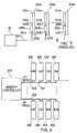
- FIG. 11depicts a memory subsystem with cached data that may be utilized by exemplary embodiments of the present invention.
- the memory subsystemincludes a memory controller 1108 with a cache directory 1106 .
- the first memory module 806(labeled in FIG. 11 as “first”) connected to the memory controller 1108 includes a cache buffer device 1102 with cache data 1104 .
- the second memory module 806(labeled in FIG. 11 as “second”) in the chain includes a buffer device 1002 as described previously herein.
- the cache buffer device 1102operates in the same manner as the previously described buffer device 1002 with the addition of cache functions.
- the memory controller 1108 depicted in FIG. 11operates in the same manner as the previously described memory controller 802 with the addition of cache functions.
- the cache directory 1106is separately accessible by the memory controller 1108 because it is contained within the memory controller 802 .
- the cache directory 1106may be located externally to the memory controller 1108 but accessible by the memory controller 1108 .
- Accesses to the cache data 1104also referred to in the art as “level 3 data” or “L3 data” are explicitly addressed by the memory controller 1108 .
- the latency of the cache readswill be less than the latency of reads to the memory devices 1004 .
- the cache read latencyis deterministically predetermined.
- the memory controller 1108utilizes the information in the cache directory 1106 and the cache read latency to schedule collision free read traffic in the memory subsystem.
- the cache buffer device 1102may be located on one or more of the memory modules 806 within the memory subsystem depicted in FIG. 11 . It may be located on the first memory module 806 and/or the second memory module 806 . If the cache buffer device 1102 is set to “global” and located in the first memory module 806 , then data from any of the memory modules 806 in the memory subsystem may be contained in the cache data 1104 and therefore referenced in the cache directory 1106 . Alternatively, the cache buffer device 1104 may be located in the first memory module 806 and set to “local”, which indicates that only data within the first memory module 806 will be contained in the cache data 1104 and referenced by the cache directory 1106 .
- Both the first and second memory modules 806may contain “local” cache buffer devices 1102 with cached data 1104 contents being reflected in the cache directory 1106 . Further, the first and second memory modules 806 may contain cache buffer devices 1104 that are set to “global” and cache data from any of the memory modules 806 in the memory subsystem may be contained in either of the cache buffer devices 1102 .
- the previous examplesrefer to a memory subsystem that contains two memory modules 806 , the same principles may be applied to memory subsystems with any number of memory modules 806 (e.g., one, four, eight, etc.).
- FIG. 12depicts an alternate memory subsystem with cached data that may be utilized by exemplary embodiments of the present invention.
- the first memory module 806(labeled in FIG. 12 as “first”) includes a cache buffer device 1102 set to “global” that contains cached data 1104 and the cache directory 1106 . Because the memory controller 802 does not know the contents of the cache data 1104 , it cannot predict the return time of the data associated with the read request (i.e., there is indeterminate read data latency). To support indeterminate read data latency, the first memory module 806 includes a read data tag signal on the upstream memory bus 906 that will tie a memory read request from the memory controller 802 to result data sent to the memory controller 802 .
- An extra wiremay be added to the upstream memory bus 906 between the first memory module 806 and the memory controller 802 to contain a bit associated with the read data tag signal.
- one or more existing wires on the upstream memory bus 906may be utilized to support the read data tag signal.
- the read data tag signalis sent to the first memory module 806 on the downstream memory bus 904 via one or more existing wires in the downstream memory bus 904 .
- the read data tag signal for the downstream memory bus 904may be created by combining the position of the memory module 806 in the chain with a sequence number.
- a cache buffer device 1102is plugged into the memory module 806 in the first position of the memory channel (or memory subsystem) and the cache buffer device 1102 is set to “global”, then the read data tag signal is utilized to identify which read request corresponds to the returning data.
- Memory read requestsare issued by the memory controller 802 to the memory channel without knowledge of the cached status of the data at the requested address. If the requested address is found to be cached, then the data at the requested address will be returned immediately by the cache buffer device 1102 , thus improving read data latency and system performance. If the requested address is not found in the cache, it will be returned from the main memory devices (e.g., SDRAMS 1004 ) with the standard read data latency. All memory addressable in the channel are potentially cached by the cache buffer device 1102 when the cache buffer device 1102 is located on a memory module 806 in the first position in the memory channel and the cache buffer device 1102 is set to “global.”
- all memory modules 806include the optional read data tag signal on their upstream controller interfaces (i.e., the upstream memory bus 906 ).
- Each segment (i.e., between each of the memory modules 806 and between the first memory module 806 and the memory controller 802 ) of the upstream memory bus 906includes an extra bit for the read data tag signal or utilize an existing bit for the read data tag signal.
- Each segmentwill contain a read data tag in cases where the cache buffer device 1102 is set to “local” and will only operate on the memory addresses that reside on the local memory module 806 .
- the read data tagmay be utilized to perform data merging between data local to the memory module 806 and data being received via the upstream memory bus 906 .
- the decoding of the read data tag and local data arbitration at each memory module 806 in the memory channelmay add appreciable latency to all memory read operations.
- the added latency associated with this embodimentis more than the added latency associated with the previous embodiment where the read data tag signal is limited to the first memory module 806 in the chain.
- FIG. 13depicts a memory structure with data compression that may be utilized by exemplary embodiments of the present invention.
- Data compressionis another enhanced feature that may be optionally added to the memory subsystems described herein.
- the compression buffer device 1302includes logic macros that encode write data into a format that requires less space in the main memory devices (e.g., the SDRAMS 1004 ).
- a memory channel, or memory subsystem, with data compressionwill appear to have a much higher capacity than an uncompressed memory channel. When leveraged by the system, this additional effective capacity will result in increased performance as fewer pieces of data will need to be stored in the slower levels of system memory such as the hard disk drive.
- memory data locations that have been compressedwill typically take longer to retrieve from the memory channel due to the decompression time.
- the first memory module 806includes an optional read data tag signal on the upstream controller interface (i.e., the upstream memory bus 906 ) to allow for indeterminate read data latency. If a compression buffer device 1302 is included in the first memory module 806 in the chain (i.e., the memory module labeled “first” in FIG. 13 ) and the compression buffer device 1302 is set to “global”, then read data tag signal will be utilized. Memory read requests are issued to the memory channel by the memory controller 802 without knowledge of the compression status of the requested address. If the data at the requested address is determined to be compressed, the data at that address will be returned after decompression.
- the upstream controller interfacei.e., the upstream memory bus 906
- the compression of datawill result in improving effective channel memory capacity and system performance. If the data at the requested address is not compressed, the data at the requested address will be returned from the main memory devices (e.g., the SDRAMS 1004 ) with the standard read data latency. All data at memory addresses in the channel are potentially compressed when the compression buffer device 1302 is located in the first memory module 806 in the channel and the compression buffer device 1302 is set to “global.”
- the compression buffer device 1302is located on one or more of the memory modules 806 and set to “local.” In this case, all memory modules 806 include the optional read data tag signal on their upstream controller interfaces (i.e., the upstream memory bus 906 ). Each segment of the upstream memory bus 906 (i.e., between each of the memory modules 806 and between the first memory module 806 and the memory controller 802 ) includes an extra bit for the read data tag signal.
- the compression buffer device 1302will only operate on the memory addresses that reside on the local memory module 806 . Decoding of the read data tag and local data arbitration at each memory module 806 in the memory channel may add appreciable latency to all memory read operations. The added latency associated with this embodiment is more than the added latency associated with the previous embodiment where the read data tag signal is limited to the first memory module 806 in the chain.
- An alternate exemplary embodiment of the present inventionincludes a buffer device 1002 with the cache functions of the cache buffer device 1102 and the compression functions of the compression buffer device 1302 .
- One, both or none of the cache functions and the compression functionsmay be activated for each memory module in the memory subsystem, thereby allowing for flexibility in memory subsystem configuration.
- one or both of the cache buffer device 1102 and the compression buffer device 1302may be located included on the first memory module and set to “global.”
- FIG. 14depicts a memory structure with cached data (on the memory module 806 labeled “second”) and data compression (on the memory module 806 labeled “third”) that may be utilized by exemplary embodiments of the present invention.
- the cache buffer device 1102 and compression buffer device 1302are not located in the first memory module 806 (i.e., they are set to “local”), the read data tag is added to all segments of the upstream memory bus 906 to track the read commands in the memory subsystem.
- the caching performed by the cache buffer deviceis limited to data stored on memory devices (e.g., SDRAMS 1004 ) accessible by the second memory module 806 .
- the compression performed by the compression buffer device 1302is limited to data stored on memory devices accessible by the third memory module 806 .
- Exemplary embodiments of the present inventionmay be utilized to improve the performance of the entire memory subsystem.
- Cache and/or data compressionmay be included in a buffer device 1002 in the first memory module 806 in the chain and apply to all data in the memory subsystem. If global caching is activated, then the cache buffer device 1102 in the first memory module 806 includes cache data for data that may be addressed by any of the memory modules 806 in the memory subsystem. Similarly, if global data compression is activated, then the compression buffer device 1302 in the first memory module provides data compression (and decompression) for data that may be addressed by any of the memory modules 806 in the memory subsystem
- Alternate exemplary embodiments of the present inventionmay be utilized to improve the performance of particular memory modules 806 within the memory subsystem.
- Local cache and/or data compressionmay be included in a buffer device 1002 in a selected memory module 806 and apply to data accessible by the selected memory module 806 . In this manner, the performance for selected memory modules 806 may be improved by utilizing exemplary embodiments of the present invention.
- the embodiments of the inventionmay be embodied in the form of computer-implemented processes and apparatuses for practicing those processes.
- Embodiments of the inventionmay also be embodied in the form of computer program code containing instructions embodied in tangible media, such as floppy diskettes, CD-ROMs, hard drives, or any other computer-readable storage medium, wherein, when the computer program code is loaded into and executed by a computer, the computer becomes an apparatus for practicing the invention.
- the present inventioncan also be embodied in the form of computer program code, for example, whether stored in a storage medium, loaded into and/or executed by a computer, or transmitted over some transmission medium, such as over electrical wiring or cabling, through fiber optics, or via electromagnetic radiation, wherein, when the computer program code is loaded into and executed by a computer, the computer becomes an apparatus for practicing the invention.
- computer program code segmentsconfigure the microprocessor to create specific logic circuits.
Landscapes
- Engineering & Computer Science (AREA)
- Theoretical Computer Science (AREA)
- Physics & Mathematics (AREA)
- General Engineering & Computer Science (AREA)
- General Physics & Mathematics (AREA)
- Memory System Of A Hierarchy Structure (AREA)
- Dram (AREA)
Abstract
Description
This application is a continuation application of U.S. Ser. No. 10/977,846, filed Oct. 29, 2004, now U.S. Pat. No. 7,277,988, the contents of which are incorporated by reference herein in their entirety.
The invention relates to a memory subsystem and, in particular, to providing data caching and data compression in a memory subsystem.
Computer memory subsystems have evolved over the years, but continue to retain many consistent attributes. Computer memory subsystems from the early 1980's, such as the one disclosed in U.S. Pat. No. 4,475,194 to LaVallee et al., of common assignment herewith, included a memory controller, a memory assembly (contemporarily called a basic storage module (BSM) by the inventors) with array devices, buffers, terminators and ancillary timing and control functions, as well as several point-to-point busses to permit each memory assembly to communicate with the memory controller via its own point-to-point address and data bus.FIG. 1 depicts an example of this early 1980 computer memory subsystem with two BSMs, a memory controller, a maintenance console, and point-to-point address and data busses connecting the BSMs and the memory controller.
As shown inFIG. 5 , memory subsystems were often constructed with a memory controller connected either to a single memory module, or to two or more memory modules interconnected on a ‘stub’ bus.FIG. 5 is a simplified example of a multi-drop stub bus memory structure, similar to the one shown inFIG. 3 . This structure offers a reasonable tradeoff between cost, performance, reliability and upgrade capability, but has inherent limits on the number of modules that may be attached to the stub bus. The limit on the number of modules that may be attached to the stub bus is directly related to the data rate of the information transferred over the bus. As data rates increase, the number and length of the stubs must be reduced to ensure robust memory operation. Increasing the speed of the bus generally results in a reduction in modules on the bus with the optimal electrical interface being one in which a single module is directly connected to a single controller, or a point-to-point interface with few, if any, stubs that will result in reflections and impedance discontinuities. As most memory modules are sixty-four or seventy-two bits in data width, this structure also requires a large number of pins to transfer address, command, and data. One hundred and twenty pins are identified inFIG. 5 as being a representative pincount.
One drawback to the use of a daisy chain bus is associated with providing enhanced capabilities such as data caching and data compression. Adding enhanced capabilities may result in an indeterminate read data latency because the amount of time required to read a particular item of data cannot be pre-determined by the memory controller. The read latency will depend on several varying factors such as whether the data is located in a cache and whether the data has to be decompressed before being returned to the memory controller. However, the ability to add data caching and/or data compression in a pluggable fashion to selected modules in a daisy chain bus is desirable because these enhanced capabilities may lead to improved performance and space savings within a memory subsystem.
Exemplary embodiments of the present invention include a cascaded interconnect system including a memory controller, one or more memory modules, an upstream memory bus and a downstream memory bus. The one or more memory modules include a first memory module with cache data. The memory modules and the memory controller are interconnected by a packetized multi-transfer interface via the downstream memory bus and the upstream memory bus. The first memory module and the memory controller are in direct communication via the upstream memory bus and the downstream memory bus.
Another exemplary embodiment of the present invention includes a memory controller, one or more memory modules, an upstream memory bus and a downstream memory bus. The one or more memory modules each include memory modules a plurality of corresponding memory devices. At least one of the memory modules includes cache data sourced from the corresponding memory devices on the memory module and a cache directory corresponding to the cache data. The memory modules and the memory controller are interconnected by a packetized multi-transfer interface via the downstream memory bus and the upstream memory bus. In addition, the memory controller utilizes a read data tag on data read requests sent via the downstream memory bus and the read data tag on data return results received via the upstream memory bus to match the data read requests with the data return results.
Another exemplary embodiment of the present invention includes a memory controller, one or more memory modules, an upstream memory bus and a downstream memory bus. The one or more memory modules include a first memory module with a data compression module for compressing and decompressing data stored on the memory modules. The memory modules and the memory controller are interconnected by a packetized multi-transfer interface via the downstream memory bus and the upstream memory bus. The first memory module and the memory controller are in direct communication via the upstream memory bus and the downstream memory bus.
A further exemplary embodiment of the present invention includes a cascaded interconnect system with a memory controller, one or more memory modules, an upstream memory bus and a downstream memory bus. The one or more memory modules each include a plurality of corresponding memory devices and at least one of the memory modules includes a data compression module. The memory modules and the memory controller are interconnected by a packetized multi-transfer interface via the downstream memory bus and the upstream memory bus. In addition, the memory controller utilizes a read data tag on data read requests sent via the downstream memory bus and the read data tag on data return results received via the upstream memory bus to match the data read requests with the data return results.
A further exemplary embodiment of the present invention includes a method for providing data caching in a memory system. The method includes receiving a request at a selected memory module to read data at a specified data address. The request is from a memory controller in a cascaded memory system and the selected memory module is one of one or more memory modules included in the cascaded memory system. A cache directory is searched for the data address. The data is read from cache data in response to locating the data address in the cache directory. The data is read from one of the memory devices in response to not locating the data address in the cache directory. The data is transmitted to the memory controller.
A further exemplary embodiment of the present invention includes a method for providing data compression in a memory system. The method includes receiving a request at a selected memory module to read data at a specified data address. The request comes from a memory controller in a cascaded memory system and the selected memory module is one of one or more memory modules included in the cascaded memory system. It is determined if the data is compressed and the data is decompressed if it is determined to be compressed. The data is then transmitted to the memory controller.
A further exemplary embodiment of the present invention includes a storage medium encoded with machine readable computer program code for providing data caching in a memory subsystem. The storage medium includes instructions for causing a computer to implement a method. The method includes receiving a request at a selected memory module to read data at a specified data address. The request is from a memory controller in a cascaded memory system and the selected memory module is one of one or more memory modules included in the cascaded memory system. A cache directory is searched for the data address. The data is read from cache data in response to locating the data address in the cache directory. The data is read from one of the memory devices in response to not locating the data address in the cache directory. The data is transmitted to the memory controller.
A further exemplary embodiment of the present invention includes a storage medium encoded with machine readable computer program code for providing data compression in a memory subsystem. The storage medium includes instructions for causing a computer to implement a method. The method includes receiving a request at a selected memory module to read data at a specified data address. The request comes from a memory controller in a cascaded memory system and the selected memory module is one of one or more memory modules included in the cascaded memory system. It is determined if the data is compressed and the data is decompressed if it is determined to be compressed. The data is then transmitted to the memory controller.
Referring now to the drawings wherein like elements are numbered alike in the several FIGURES:
Exemplary embodiments of the present invention provide an enhanced memory subsystem (or memory channel) by including data caching capability in one or more memory modules within a cascaded memory subsystem. In embodiments where the memory controller has access to a cache directory for the memory subsystem, the deterministic nature of the controller interface protocol utilized by the memory subsystem is preserved. When the memory controller has access to the cache directory, reads to the cache data can be predetermined and specifically requested by the memory controller. Thus, the read data return from such reads to the cache data may be scheduled using standard mechanisms.
Additional embodiments of the present invention provide for a memory subsystem where the cache directory does not reside in the memory controller and is not accessible by the memory controller. In this case, the addition of cache to the memory subsystem results in indeterminate read data latencies. A tag signal is added to the upstream controller interface frame format so that returned read data may be identified by the memory controller. This read data identification removes the requirement that the memory controller be able to predict the exact return time of each read request. The ability to handle indeterminate read data latency allows the memory modules in the memory channel to utilize enhanced features (e.g., data caching and data compression) that modify the normally predictable read data return times.
Although point-to-point interconnects permit higher data rates, overall memory subsystem efficiency must be achieved by maintaining a reasonable number ofmemory modules 806 and memory devices per channel (historically four memory modules with four to thirty-six chips per memory module, but as high as eight memory modules per channel and as few as one memory module per channel). Using a point-to-point bus necessitates a bus re-drive function on each memory module to permit memory modules to be cascaded such that each memory module is interconnected to other memory modules, as well as to thememory controller 802.
An exemplary embodiment of the present invention includes two uni-directional busses between thememory controller 802 andmemory module 806a(“DIMM # 1”), as well as between eachsuccessive memory module 806b-d(“DIMM # 2”, “DIMM # 3” and “DIMM # 4”) in the cascaded memory structure. Thedownstream memory bus 904 is comprised of twenty-two single-ended signals and a differential clock pair. Thedownstream memory bus 904 is used to transfer address, control, write data and bus-level error code correction (ECC) bits downstream from thememory controller 802, over several clock cycles, to one or more of thememory modules 806 installed on the cascaded memory channel. Theupstream memory bus 902 is comprised of twenty-three single-ended signals and a differential clock pair, and is used to transfer read data and bus-level ECC bits upstream from thesourcing memory module 806 to thememory controller 802. Because theupstream memory bus 902 and thedownstream memory bus 904 are unidirectional and operate independently, read data, write data and memory commands may be transmitted simultaneously. This increases effective memory subsystem bandwidth and may result in higher system performance. Using this memory structure, and a four to one data rate multiplier between the DRAM data rate (e.g., 400 to 800 Mb/s per pin) and the unidirectional memory bus data rate (e.g., 1.6 to 3.2 Gb/s per pin), thememory controller 802 signal pincount, per memory channel, is reduced from approximately one hundred and twenty pins to about fifty pins.
Thememory controller 802 interfaces to thememory modules 806 via a pair of high speed busses (or channels). The downstream memory bus904 (outbound from the memory controller802) interface has twenty-four pins and the upstream memory bus902 (inbound to the memory controller802) interface has twenty-five pins. The high speed channels each include a clock pair (differential), a spare bit lane, ECC syndrome bits and the remainder of the bits pass information (based on the operation underway). Due to the cascaded memory structure, all nets are point-to-point, allowing reliable high-speed communication that is independent of the number ofmemory modules 806 installed. Whenever amemory module 806 receives a packet on either bus, it re-synchronizes the command to the internal clock and re-drives the command to thenext memory module 806 in the chain (if one exists).
As described previously, thememory controller 802 interfaces to thememory module 806 via a pair of high speed channels (i.e., thedownstream memory bus 904 and the upstream memory bus902). The downstream (outbound from the memory controller802) interface has twenty-four pins and the upstream (inbound to the memory controller802) has twenty-five pins. The high speed channels each consist of a clock pair (differential), as well as single ended signals. Due to the cascade memory structure, all nets are point to point, allowing reliable high-speed communication that is independent of the number ofmemory modules 806 installed. The differential clock received from the downstream interface is used as the reference clock for the buffer device PLL and is therefore the source of alllocal buffer device 1002 clocks. Whenever thememory module 806 receives a packet on either bus, it re-synchronizes it to the local clock and drives it to thenext memory module 806 ormemory controller 802, in the chain (if one exists).
In the configuration depicted inFIG. 11 , thecache directory 1106 is separately accessible by the memory controller1108 because it is contained within thememory controller 802. Alternatively, thecache directory 1106 may be located externally to the memory controller1108 but accessible by the memory controller1108. Accesses to the cache data1104 (also referred to in the art as “level 3 data” or “L3 data”) are explicitly addressed by the memory controller1108. As is known in the art, the latency of the cache reads will be less than the latency of reads to thememory devices 1004. In the exemplary configuration depicted inFIG. 11 , the cache read latency is deterministically predetermined. The memory controller1108 utilizes the information in thecache directory 1106 and the cache read latency to schedule collision free read traffic in the memory subsystem.
Thecache buffer device 1102 may be located on one or more of thememory modules 806 within the memory subsystem depicted inFIG. 11 . It may be located on thefirst memory module 806 and/or thesecond memory module 806. If thecache buffer device 1102 is set to “global” and located in thefirst memory module 806, then data from any of thememory modules 806 in the memory subsystem may be contained in thecache data 1104 and therefore referenced in thecache directory 1106. Alternatively, thecache buffer device 1104 may be located in thefirst memory module 806 and set to “local”, which indicates that only data within thefirst memory module 806 will be contained in thecache data 1104 and referenced by thecache directory 1106. Both the first andsecond memory modules 806 may contain “local”cache buffer devices 1102 with cacheddata 1104 contents being reflected in thecache directory 1106. Further, the first andsecond memory modules 806 may containcache buffer devices 1104 that are set to “global” and cache data from any of thememory modules 806 in the memory subsystem may be contained in either of thecache buffer devices 1102. The previous examples refer to a memory subsystem that contains twomemory modules 806, the same principles may be applied to memory subsystems with any number of memory modules806 (e.g., one, four, eight, etc.).
If acache buffer device 1102 is plugged into thememory module 806 in the first position of the memory channel (or memory subsystem) and thecache buffer device 1102 is set to “global”, then the read data tag signal is utilized to identify which read request corresponds to the returning data. Memory read requests are issued by thememory controller 802 to the memory channel without knowledge of the cached status of the data at the requested address. If the requested address is found to be cached, then the data at the requested address will be returned immediately by thecache buffer device 1102, thus improving read data latency and system performance. If the requested address is not found in the cache, it will be returned from the main memory devices (e.g., SDRAMS1004) with the standard read data latency. All memory addressable in the channel are potentially cached by thecache buffer device 1102 when thecache buffer device 1102 is located on amemory module 806 in the first position in the memory channel and thecache buffer device 1102 is set to “global.”
In an alternate exemplary embodiment of the present invention, allmemory modules 806 include the optional read data tag signal on their upstream controller interfaces (i.e., the upstream memory bus906). Each segment (i.e., between each of thememory modules 806 and between thefirst memory module 806 and the memory controller802) of theupstream memory bus 906 includes an extra bit for the read data tag signal or utilize an existing bit for the read data tag signal. Each segment will contain a read data tag in cases where thecache buffer device 1102 is set to “local” and will only operate on the memory addresses that reside on thelocal memory module 806. In addition, the read data tag may be utilized to perform data merging between data local to thememory module 806 and data being received via theupstream memory bus 906. The decoding of the read data tag and local data arbitration at eachmemory module 806 in the memory channel may add appreciable latency to all memory read operations. The added latency associated with this embodiment is more than the added latency associated with the previous embodiment where the read data tag signal is limited to thefirst memory module 806 in the chain.
In exemplary embodiments, such as the one depicted inFIG. 13 , thefirst memory module 806 includes an optional read data tag signal on the upstream controller interface (i.e., the upstream memory bus906) to allow for indeterminate read data latency. If acompression buffer device 1302 is included in thefirst memory module 806 in the chain (i.e., the memory module labeled “first” inFIG. 13 ) and thecompression buffer device 1302 is set to “global”, then read data tag signal will be utilized. Memory read requests are issued to the memory channel by thememory controller 802 without knowledge of the compression status of the requested address. If the data at the requested address is determined to be compressed, the data at that address will be returned after decompression. The compression of data will result in improving effective channel memory capacity and system performance. If the data at the requested address is not compressed, the data at the requested address will be returned from the main memory devices (e.g., the SDRAMS1004) with the standard read data latency. All data at memory addresses in the channel are potentially compressed when thecompression buffer device 1302 is located in thefirst memory module 806 in the channel and thecompression buffer device 1302 is set to “global.”
In alternate exemplary embodiments of the present invention, thecompression buffer device 1302 is located on one or more of thememory modules 806 and set to “local.” In this case, allmemory modules 806 include the optional read data tag signal on their upstream controller interfaces (i.e., the upstream memory bus906). Each segment of the upstream memory bus906 (i.e., between each of thememory modules 806 and between thefirst memory module 806 and the memory controller802) includes an extra bit for the read data tag signal. Here, thecompression buffer device 1302 will only operate on the memory addresses that reside on thelocal memory module 806. Decoding of the read data tag and local data arbitration at eachmemory module 806 in the memory channel may add appreciable latency to all memory read operations. The added latency associated with this embodiment is more than the added latency associated with the previous embodiment where the read data tag signal is limited to thefirst memory module 806 in the chain.
An alternate exemplary embodiment of the present invention includes abuffer device 1002 with the cache functions of thecache buffer device 1102 and the compression functions of thecompression buffer device 1302. One, both or none of the cache functions and the compression functions may be activated for each memory module in the memory subsystem, thereby allowing for flexibility in memory subsystem configuration. Further, one or both of thecache buffer device 1102 and thecompression buffer device 1302 may be located included on the first memory module and set to “global.”
Exemplary embodiments of the present invention may be utilized to improve the performance of the entire memory subsystem. Cache and/or data compression may be included in abuffer device 1002 in thefirst memory module 806 in the chain and apply to all data in the memory subsystem. If global caching is activated, then thecache buffer device 1102 in thefirst memory module 806 includes cache data for data that may be addressed by any of thememory modules 806 in the memory subsystem. Similarly, if global data compression is activated, then thecompression buffer device 1302 in the first memory module provides data compression (and decompression) for data that may be addressed by any of thememory modules 806 in the memory subsystem
Alternate exemplary embodiments of the present invention may be utilized to improve the performance ofparticular memory modules 806 within the memory subsystem. Local cache and/or data compression may be included in abuffer device 1002 in a selectedmemory module 806 and apply to data accessible by the selectedmemory module 806. In this manner, the performance for selectedmemory modules 806 may be improved by utilizing exemplary embodiments of the present invention.
As described above, the embodiments of the invention may be embodied in the form of computer-implemented processes and apparatuses for practicing those processes. Embodiments of the invention may also be embodied in the form of computer program code containing instructions embodied in tangible media, such as floppy diskettes, CD-ROMs, hard drives, or any other computer-readable storage medium, wherein, when the computer program code is loaded into and executed by a computer, the computer becomes an apparatus for practicing the invention. The present invention can also be embodied in the form of computer program code, for example, whether stored in a storage medium, loaded into and/or executed by a computer, or transmitted over some transmission medium, such as over electrical wiring or cabling, through fiber optics, or via electromagnetic radiation, wherein, when the computer program code is loaded into and executed by a computer, the computer becomes an apparatus for practicing the invention. When implemented on a general-purpose microprocessor, the computer program code segments configure the microprocessor to create specific logic circuits.
While the invention has been described with reference to exemplary embodiments, it will be understood by those skilled in the art that various changes may be made and equivalents may be substituted for elements thereof without departing from the scope of the invention. In addition, many modifications may be made to adapt a particular situation or material to the teachings of the invention without departing from the essential scope thereof. Therefore, it is intended that the invention not be limited to the particular embodiment disclosed as the best mode contemplated for carrying out this invention, but that the invention will include all embodiments falling within the scope of the appended claims. Moreover, the use of the terms first, second, etc. do not denote any order or importance, but rather the terms first, second, etc. are used to distinguish one element from another.
Claims (15)
1. A cascaded interconnect system comprising:
a memory controller operable with indeterminate data response times;
one or more memory devices;
one or more memory modules, wherein at least one of the memory modules includes a cache containing data sourced from at least a subset of the one or more memory devices;
an upstream memory bus; and
a downstream memory bus, wherein the memory modules and the memory controller are interconnected by a packetized multi-transfer interface via the downstream memory bus and the upstream memory bus, and data responses to data read requests sourced from the cache include tag information to correlate the data responses to the data read requests.
2. The system ofclaim 1 wherein the memory controller includes a cache directory corresponding to the cache.
3. The system ofclaim 1 wherein at least one of the memory modules including the cache further includes a cache directory corresponding to the cache.
4. The system ofclaim 1 wherein the upstream memory bus includes one or more wires for the tag information.
5. The system ofclaim 1 wherein the cache is located on a first memory module in the one or more memory modules and at least a subset of the data in the cache is sourced from a memory device located on a second memory module in the one or more memory modules, the first memory module and the second memory module being different memory modules.
6. The system ofclaim 1 wherein at least one of the memory modules includes a data compression module for compressing and decompressing data read from and written to the one or more memory devices.
7. A cascaded interconnect system comprising:
a memory controller operable with indeterminate data response times;
one or more memory devices;
one or more memory modules, wherein at least one of the memory modules includes one or more of the memory devices located on the memory module, cache data sourced from the memory devices located on the memory module, and a cache directory corresponding to the cache data;
an upstream memory bus; and
a downstream memory bus, wherein the memory modules and the memory controller are interconnected by a packetized multi-transfer interface via the downstream memory bus and the upstream memory bus, and the memory controller utilizes a read data tag on data read requests sent from the memory controller via the downstream memory bus and the read data tag on data return results received by the memory controller via the upstream memory bus to match the data read requests with the data return results.
8. The system ofclaim 7 wherein at least one of the one or more memory modules includes a data compression module for compressing and decompressing data read from and written to the one or more memory devices.
9. A method for providing data caching in a memory system, the method comprising:
receiving a request at a selected memory module to read data at a specified data address, the request from a memory controller operable with indeterminate data response times in a cascaded memory system and wherein the selected memory module is one of one or more memory modules included in the cascaded memory system;
searching a cache directory for the data address;
reading the data from cache in response to locating the data address in the cache directory;
reading the data from one or more memory devices in response to not locating the data address in the cache directory; and
transmitting the data to the memory controller; and
transmitting tag information along with the data to correlate the data to the request if the data was sourced from the cache.
10. The method ofclaim 9 wherein the cache directory is located on the memory controller.
11. The method ofclaim 9 wherein the cache directory is located on the selected memory module, the receiving a request includes receiving a read data tag associated with the request and the transmitting the data includes transmitting the read data tag.
12. The method ofclaim 9 wherein the selected memory module is in direct communication with the memory controller and data in the cache is sourced from one or more memory devices located on an other memory module.
13. The method ofclaim 9 wherein data in the cache is sourced from data located on one or more memory devices on the selected memory module.
14. The method ofclaim 9 wherein the selected memory module further includes a data compression module.
15. A storage medium encoded with machine readable computer program code for providing data caching in a memory subsystem, the storage medium including instructions for causing a computer to implement a method comprising:
receiving a request at a selected memory module to read data at a specified data address, the request from a memory controller operable with indeterminate data response times in a cascaded memory system and wherein the selected memory module is one of one or more memory modules included in the cascaded memory system;
searching a cache directory for the data address;
reading the data from cache in response to locating the data address in the cache directory;
reading the data from one or more memory devices in response to not locating the data address in the cache directory; and
transmitting the data to the memory controller; and
transmitting tag information along with the data to correlate the data to the request if the data was sourced from the cache.
Priority Applications (1)
| Application Number | Priority Date | Filing Date | Title |
|---|---|---|---|
| US11/780,048US7451273B2 (en) | 2004-10-29 | 2007-07-19 | System, method and storage medium for providing data caching and data compression in a memory subsystem |
Applications Claiming Priority (2)
| Application Number | Priority Date | Filing Date | Title |
|---|---|---|---|
| US10/977,846US7277988B2 (en) | 2004-10-29 | 2004-10-29 | System, method and storage medium for providing data caching and data compression in a memory subsystem |
| US11/780,048US7451273B2 (en) | 2004-10-29 | 2007-07-19 | System, method and storage medium for providing data caching and data compression in a memory subsystem |
Related Parent Applications (1)
| Application Number | Title | Priority Date | Filing Date |
|---|---|---|---|
| US10/977,846ContinuationUS7277988B2 (en) | 2004-10-29 | 2004-10-29 | System, method and storage medium for providing data caching and data compression in a memory subsystem |
Publications (2)
| Publication Number | Publication Date |
|---|---|
| US20080016281A1 US20080016281A1 (en) | 2008-01-17 |
| US7451273B2true US7451273B2 (en) | 2008-11-11 |
Family
ID=36263478
Family Applications (3)
| Application Number | Title | Priority Date | Filing Date |
|---|---|---|---|
| US10/977,846Expired - Fee RelatedUS7277988B2 (en) | 2004-10-29 | 2004-10-29 | System, method and storage medium for providing data caching and data compression in a memory subsystem |
| US11/772,922Expired - Fee RelatedUS7480759B2 (en) | 2004-10-29 | 2007-07-03 | System, method and storage medium for providing data caching and data compression in a memory subsystem |
| US11/780,048Expired - Fee RelatedUS7451273B2 (en) | 2004-10-29 | 2007-07-19 | System, method and storage medium for providing data caching and data compression in a memory subsystem |
Family Applications Before (2)
| Application Number | Title | Priority Date | Filing Date |
|---|---|---|---|
| US10/977,846Expired - Fee RelatedUS7277988B2 (en) | 2004-10-29 | 2004-10-29 | System, method and storage medium for providing data caching and data compression in a memory subsystem |
| US11/772,922Expired - Fee RelatedUS7480759B2 (en) | 2004-10-29 | 2007-07-03 | System, method and storage medium for providing data caching and data compression in a memory subsystem |
Country Status (1)
| Country | Link |
|---|---|
| US (3) | US7277988B2 (en) |
Families Citing this family (35)
| Publication number | Priority date | Publication date | Assignee | Title |
|---|---|---|---|---|
| JP4094370B2 (en)* | 2002-07-31 | 2008-06-04 | エルピーダメモリ株式会社 | Memory module and memory system |
| US20070005902A1 (en)* | 2004-12-07 | 2007-01-04 | Ocz Technology Group, Inc. | Integrated sram cache for a memory module and method therefor |
| US7426649B2 (en)* | 2005-02-09 | 2008-09-16 | International Business Machines Corporation | Power management via DIMM read operation limiter |
| US7373471B2 (en)* | 2005-02-09 | 2008-05-13 | International Business Machines Corporation | Executing background writes to idle DIMMs |
| US20060174431A1 (en)* | 2005-02-09 | 2006-08-10 | Dr. Fresh, Inc. | Electric toothbrush |
| US7447831B2 (en)* | 2006-05-18 | 2008-11-04 | International Business Machines Corporation | Memory systems for automated computing machinery |
| US7865641B2 (en)* | 2006-09-29 | 2011-01-04 | Qimonda Ag | Synchronization and scheduling of a dual master serial channel |
| US8745315B2 (en)* | 2006-11-06 | 2014-06-03 | Rambus Inc. | Memory Systems and methods supporting volatile and wear-leveled nonvolatile physical memory |
| WO2008121559A1 (en) | 2007-03-30 | 2008-10-09 | Rambus Incorporated | System including hierarchical memory modules having different types of integrated circuit memory devices |
| KR100981884B1 (en) | 2008-01-08 | 2010-09-14 | 한국과학기술원 | How to Manage Prefetching Data on Computer Storage Devices |
| US8516185B2 (en)* | 2009-07-16 | 2013-08-20 | Netlist, Inc. | System and method utilizing distributed byte-wise buffers on a memory module |
| US7717752B2 (en)* | 2008-07-01 | 2010-05-18 | International Business Machines Corporation | 276-pin buffered memory module with enhanced memory system interconnect and features |
| US20100005212A1 (en)* | 2008-07-01 | 2010-01-07 | International Business Machines Corporation | Providing a variable frame format protocol in a cascade interconnected memory system |
| US20100005220A1 (en)* | 2008-07-01 | 2010-01-07 | International Business Machines Corporation | 276-pin buffered memory module with enhanced memory system interconnect and features |
| US20100005218A1 (en)* | 2008-07-01 | 2010-01-07 | International Business Machines Corporation | Enhanced cascade interconnected memory system |
| US20100005219A1 (en)* | 2008-07-01 | 2010-01-07 | International Business Machines Corporation | 276-pin buffered memory module with enhanced memory system interconnect and features |
| US20100005214A1 (en)* | 2008-07-01 | 2010-01-07 | International Business Machines Corporation | Enhancing bus efficiency in a memory system |
| US20100005206A1 (en)* | 2008-07-01 | 2010-01-07 | International Business Machines Corporation | Automatic read data flow control in a cascade interconnect memory system |
| JP5214736B2 (en)* | 2008-09-12 | 2013-06-19 | 株式会社日立製作所 | Semiconductor device and information processing system |
| US8612676B2 (en) | 2010-12-22 | 2013-12-17 | Intel Corporation | Two-level system main memory |
| EP3364304B1 (en) | 2011-09-30 | 2022-06-15 | INTEL Corporation | Memory channel that supports near memory and far memory access |
| US9003160B2 (en) | 2012-08-03 | 2015-04-07 | International Business Machines Corporation | Active buffered memory |
| US9575755B2 (en) | 2012-08-03 | 2017-02-21 | International Business Machines Corporation | Vector processing in an active memory device |
| US9569211B2 (en) | 2012-08-03 | 2017-02-14 | International Business Machines Corporation | Predication in a vector processor |
| US9632777B2 (en) | 2012-08-03 | 2017-04-25 | International Business Machines Corporation | Gather/scatter of multiple data elements with packed loading/storing into/from a register file entry |
| US9594724B2 (en) | 2012-08-09 | 2017-03-14 | International Business Machines Corporation | Vector register file |
| US8972782B2 (en) | 2012-11-09 | 2015-03-03 | International Business Machines Corporation | Exposed-pipeline processing element with rollback |
| US9335950B2 (en)* | 2013-03-15 | 2016-05-10 | Western Digital Technologies, Inc. | Multiple stream compression and formatting of data for data storage systems |
| US9448738B2 (en) | 2013-03-15 | 2016-09-20 | Western Digital Technologies, Inc. | Compression and formatting of data for data storage systems |
| US9274978B2 (en) | 2013-06-10 | 2016-03-01 | Western Digital Technologies, Inc. | Migration of encrypted data for data storage systems |
| US9514061B1 (en)* | 2015-05-20 | 2016-12-06 | Qualcomm Incorporated | Method and apparatus for cache tag compression |
| US9460791B1 (en)* | 2015-12-08 | 2016-10-04 | Inphi Corporation | Data clock synchronization in hybrid memory modules |
| US10067706B2 (en) | 2016-03-31 | 2018-09-04 | Qualcomm Incorporated | Providing memory bandwidth compression using compression indicator (CI) hint directories in a central processing unit (CPU)-based system |
| US10216685B1 (en)* | 2017-07-19 | 2019-02-26 | Agiga Tech Inc. | Memory modules with nonvolatile storage and rapid, sustained transfer rates |
| CN114691571B (en)* | 2020-12-28 | 2024-05-28 | 上海寒武纪信息科技有限公司 | Data processing method, reordering buffer and interconnection device |
Citations (224)
| Publication number | Priority date | Publication date | Assignee | Title |
|---|---|---|---|---|
| US2842682A (en) | 1956-09-04 | 1958-07-08 | Ibm | Reversible shift register |
| US3333253A (en) | 1965-02-01 | 1967-07-25 | Ibm | Serial-to-parallel and parallel-toserial buffer-converter using a core matrix |
| US3395400A (en) | 1966-04-26 | 1968-07-30 | Bell Telephone Labor Inc | Serial to parallel data converter |
| US3825904A (en) | 1973-06-08 | 1974-07-23 | Ibm | Virtual memory system |
| US4028675A (en) | 1973-05-14 | 1977-06-07 | Hewlett-Packard Company | Method and apparatus for refreshing semiconductor memories in multi-port and multi-module memory system |
| US4135240A (en) | 1973-07-09 | 1979-01-16 | Bell Telephone Laboratories, Incorporated | Protection of data file contents |
| JPS59153353A (en) | 1983-02-22 | 1984-09-01 | Nec Corp | Data transmission system |
| US4472780A (en) | 1981-09-28 | 1984-09-18 | The Boeing Company | Fly-by-wire lateral control system |
| US4475194A (en) | 1982-03-30 | 1984-10-02 | International Business Machines Corporation | Dynamic replacement of defective memory words |
| JPS59153353U (en) | 1983-04-01 | 1984-10-15 | 石川島播磨重工業株式会社 | Shaft sealing device for high temperature atmosphere such as blast furnace |
| US4486739A (en) | 1982-06-30 | 1984-12-04 | International Business Machines Corporation | Byte oriented DC balanced (0,4) 8B/10B partitioned block transmission code |
| US4641263A (en) | 1982-05-17 | 1987-02-03 | Digital Associates Corporation | Controller system or emulating local parallel minicomputer/printer interface and transferring serial data to remote line printer |
| US4654857A (en) | 1981-10-01 | 1987-03-31 | Stratus Computer, Inc. | Digital data processor with high reliability |
| US4723120A (en) | 1986-01-14 | 1988-02-02 | International Business Machines Corporation | Method and apparatus for constructing and operating multipoint communication networks utilizing point-to point hardware and interfaces |
| US4740916A (en) | 1985-12-19 | 1988-04-26 | International Business Machines Corporation | Reconfigurable contiguous address space memory system including serially connected variable capacity memory modules and a split address bus |
| US4796231A (en) | 1985-01-22 | 1989-01-03 | Texas Instruments Incorporated | Serial accessed semiconductor memory with reconfigurable shift registers |
| US4803485A (en) | 1987-03-23 | 1989-02-07 | Amp Incorporated | Lan communication system and medium adapter for use therewith |
| US4833605A (en) | 1984-08-16 | 1989-05-23 | Mitsubishi Denki Kabushiki Kaisha | Cascaded information processing module having operation unit, parallel port, and serial port for concurrent data transfer and data processing |
| US4839534A (en) | 1986-10-16 | 1989-06-13 | Siemens Aktiengesellschaft | Method and apparatus for establishing a system clock in response to the level of one of two clock signal sources |
| US4943984A (en) | 1988-06-24 | 1990-07-24 | International Business Machines Corporation | Data processing system parallel data bus having a single oscillator clocking apparatus |
| US4985828A (en) | 1987-03-19 | 1991-01-15 | Hitachi, Ltd. | Method and apparatus for generating a real address multiple virtual address spaces of a storage |
| US5053947A (en) | 1989-09-29 | 1991-10-01 | Allegro Microsystems, Inc. | Extended multistation bus system and method |
| EP0470734A1 (en) | 1990-08-06 | 1992-02-12 | NCR International, Inc. | Cache memory management system |
| US5177375A (en) | 1989-12-28 | 1993-01-05 | Mitsubishi Denki Kabushiki Kaisha | Power on reset circuit for semiconductor integrated circuit device |
| US5206946A (en) | 1989-10-27 | 1993-04-27 | Sand Technology Systems Development, Inc. | Apparatus using converters, multiplexer and two latches to convert SCSI data into serial data and vice versa |
| US5214747A (en) | 1990-12-24 | 1993-05-25 | Eastman Kodak Company | Segmented neural network with daisy chain control |
| US5265212A (en) | 1992-04-01 | 1993-11-23 | Digital Equipment Corporation | Sharing of bus access among multiple state machines with minimal wait time and prioritization of like cycle types |
| US5287531A (en) | 1990-10-31 | 1994-02-15 | Compaq Computer Corp. | Daisy-chained serial shift register for determining configuration of removable circuit boards in a computer system |
| US5347270A (en) | 1991-12-27 | 1994-09-13 | Mitsubishi Denki Kabushiki Kaisha | Method of testing switches and switching circuit |
| US5357621A (en) | 1990-09-04 | 1994-10-18 | Hewlett-Packard Company | Serial architecture for memory module control |
| US5375127A (en) | 1992-03-25 | 1994-12-20 | Ncr Corporation | Method and apparatus for generating Reed-Soloman error correcting code across multiple word boundaries |
| US5387911A (en) | 1992-02-21 | 1995-02-07 | Gleichert; Marc C. | Method and apparatus for transmitting and receiving both 8B/10B code and 10B/12B code in a switchable 8B/10B transmitter and receiver |
| US5394535A (en) | 1989-04-21 | 1995-02-28 | Nec Corporation | Memory access control circuit with automatic access mode determination circuitry with read-modify-write and write-per-bit operations |
| US5454091A (en) | 1990-06-29 | 1995-09-26 | Digital Equipment Corporation | Virtual to physical address translation scheme with granularity hint for identifying subsequent pages to be accessed |
| US5475690A (en) | 1994-11-10 | 1995-12-12 | Digital Equipment Corporation | Delay compensated signal propagation |
| US5513135A (en) | 1994-12-02 | 1996-04-30 | International Business Machines Corporation | Synchronous memory packaged in single/dual in-line memory module and method of fabrication |
| US5522064A (en) | 1990-10-01 | 1996-05-28 | International Business Machines Corporation | Data processing apparatus for dynamically setting timings in a dynamic memory system |
| US5544309A (en) | 1993-04-22 | 1996-08-06 | International Business Machines Corporation | Data processing system with modified planar for boundary scan diagnostics |
| US5546023A (en) | 1995-06-26 | 1996-08-13 | Intel Corporation | Daisy chained clock distribution scheme |
| US5561826A (en) | 1990-05-25 | 1996-10-01 | Silicon Systems, Inc. | Configurable architecture for serial communication |
| US5592632A (en) | 1991-11-05 | 1997-01-07 | Monolithic System Technology, Inc. | Defect tolerant integrated circuit subsystem for communication between a module and a bus controller in a wafer-scale integrated circuit system |
| US5611055A (en) | 1994-09-27 | 1997-03-11 | Novalink Technologies | Method and apparatus for implementing a PCMCIA auxiliary port connector for selectively communicating with peripheral devices |
| US5627963A (en) | 1992-04-30 | 1997-05-06 | International Business Machines Corporation | Redundant read bus for correcting defective columns in a cache memory |
| US5629685A (en) | 1995-02-23 | 1997-05-13 | International Business Machines Corporation | Segmentable addressable modular communication network hubs |
| US5661677A (en) | 1996-05-15 | 1997-08-26 | Micron Electronics, Inc. | Circuit and method for on-board programming of PRD Serial EEPROMS |
| US5684418A (en) | 1994-12-26 | 1997-11-04 | Sony Corpoation | Clock signal generator |
| JPH1011971A (en) | 1996-06-21 | 1998-01-16 | Mitsubishi Electric Corp | Semiconductor storage device |
| US5764155A (en) | 1996-04-03 | 1998-06-09 | General Electric Company | Dynamic data exchange server |
| US5822749A (en) | 1994-07-12 | 1998-10-13 | Sybase, Inc. | Database system with methods for improving query performance with cache optimization strategies |
| US5852617A (en) | 1995-12-08 | 1998-12-22 | Samsung Electronics Co., Ltd. | Jtag testing of buses using plug-in cards with Jtag logic mounted thereon |
| US5870325A (en) | 1998-04-14 | 1999-02-09 | Silicon Graphics, Inc. | Memory system with multiple addressing and control busses |
| US5872996A (en) | 1992-03-06 | 1999-02-16 | Rambus, Inc. | Method and apparatus for transmitting memory requests by transmitting portions of count data in adjacent words of a packet |
| US5917760A (en) | 1996-09-20 | 1999-06-29 | Sldram, Inc. | De-skewing data signals in a memory system |
| US5926838A (en) | 1997-03-19 | 1999-07-20 | Micron Electronics | Interface for high speed memory |
| US5928343A (en) | 1990-04-18 | 1999-07-27 | Rambus Inc. | Memory module having memory devices containing internal device ID registers and method of initializing same |
| US5930273A (en) | 1996-04-18 | 1999-07-27 | Oki Electric Industry Co., Ltd. | STM-N signal error correction coding system and method |
| US5974493A (en) | 1996-02-26 | 1999-10-26 | Mitsubishi Denki Kabushiki Kaisha | Microcomputer with processor bus having smaller width than memory bus |
| US5973951A (en) | 1992-05-19 | 1999-10-26 | Sun Microsystems, Inc. | Single in-line memory module |
| US5995405A (en) | 1998-10-27 | 1999-11-30 | Micron Technology, Inc. | Memory module with flexible serial presence detect configuration |
| US6003121A (en) | 1998-05-18 | 1999-12-14 | Intel Corporation | Single and multiple channel memory detection and sizing |
| US6038132A (en) | 1996-12-06 | 2000-03-14 | Mitsubishi Denki Kabushiki Kaisha | Memory module |
| US6049476A (en) | 1995-05-15 | 2000-04-11 | Silicon Graphics, Inc. | High memory capacity DIMM with data and state memory |
| US6076158A (en) | 1990-06-29 | 2000-06-13 | Digital Equipment Corporation | Branch prediction in high-performance processor |
| US6081868A (en) | 1993-12-15 | 2000-06-27 | Hewlett-Packard Company | System and methods for performing cache latency diagnostics in scalable parallel processing architectures including calculating CPU idle time and counting number of cache misses |
| US6085276A (en) | 1997-10-24 | 2000-07-04 | Compaq Computers Corporation | Multi-processor computer system having a data switch with simultaneous insertion buffers for eliminating arbitration interdependencies |
| US6096091A (en) | 1998-02-24 | 2000-08-01 | Advanced Micro Devices, Inc. | Dynamically reconfigurable logic networks interconnected by fall-through FIFOs for flexible pipeline processing in a system-on-a-chip |
| US6128746A (en) | 1997-08-26 | 2000-10-03 | International Business Machines Corporation | Continuously powered mainstore for large memory subsystems |
| US6145028A (en) | 1997-12-11 | 2000-11-07 | Ncr Corporation | Enhanced multi-pathing to an array of storage devices |
| US6170047B1 (en) | 1994-11-16 | 2001-01-02 | Interactive Silicon, Inc. | System and method for managing system memory and/or non-volatile memory using a memory controller with integrated compression and decompression capabilities |
| US6170059B1 (en) | 1998-07-10 | 2001-01-02 | International Business Machines Corporation | Tracking memory modules within a computer system |
| US6173382B1 (en) | 1998-04-28 | 2001-01-09 | International Business Machines Corporation | Dynamic configuration of memory module using modified presence detect data |
| US6185718B1 (en) | 1998-02-27 | 2001-02-06 | International Business Machines Corporation | Memory card design with parity and ECC for non-parity and non-ECC systems |
| US6215686B1 (en) | 1999-02-09 | 2001-04-10 | Silicon Graphics, Inc. | Memory system with switching for data isolation |
| US6219288B1 (en) | 2000-03-03 | 2001-04-17 | International Business Machines Corporation | Memory having user programmable AC timings |
| US6219760B1 (en) | 1997-06-27 | 2001-04-17 | Advanced Micro Devices, Inc. | Cache including a prefetch way for storing cache lines and configured to move a prefetched cache line to a non-prefetch way upon access to the prefetched cache line |
| US20010003839A1 (en) | 1999-12-09 | 2001-06-14 | Hidetoshi Kondo | Data access method in the network system and the network system |
| US6260127B1 (en) | 1998-07-13 | 2001-07-10 | Compaq Computer Corporation | Method and apparatus for supporting heterogeneous memory in computer systems |
| US6262493B1 (en) | 1999-10-08 | 2001-07-17 | Sun Microsystems, Inc. | Providing standby power to field replaceable units for electronic systems |
| US6292903B1 (en) | 1997-07-09 | 2001-09-18 | International Business Machines Corporation | Smart memory interface |
| US6301636B1 (en) | 1997-08-28 | 2001-10-09 | Nortel Networks Limited | Content addressable memory system with cascaded memories and self timed signals |
| US20010029566A1 (en) | 1999-12-30 | 2001-10-11 | Shin Dong Woo | Rambus DRAM |
| US6317352B1 (en) | 2000-09-18 | 2001-11-13 | Intel Corporation | Apparatus for implementing a buffered daisy chain connection between a memory controller and memory modules |
| US6321343B1 (en) | 1997-10-02 | 2001-11-20 | Kabushiki Kaisha Toshiba | Semiconductor memory system comprising synchronous DRAM and controller thereof |
| US6338113B1 (en) | 1998-06-10 | 2002-01-08 | Mitsubishi Denki Kabushiki Kaisha | Memory module system having multiple memory modules |
| US20020019926A1 (en) | 1997-12-17 | 2002-02-14 | Huppenthal Jon M. | Switch/network adapter port for clustered computers employing a chain of multi-adaptive processors in a dual in-line memory module format |
| US6357018B1 (en) | 1999-01-26 | 2002-03-12 | Dell Usa, L.P. | Method and apparatus for determining continuity and integrity of a RAMBUS channel in a computer system |
| US6370631B1 (en) | 1994-11-16 | 2002-04-09 | Interactive Silicon, Inc. | Memory controller including compression/decompression capabilities for improved data access |
| US6378018B1 (en) | 1997-10-10 | 2002-04-23 | Intel Corporation | Memory device and system including a low power interface |
| US20020059439A1 (en) | 1999-02-26 | 2002-05-16 | Arroyo Keith M. | Streaming method and system for fibre channel network devices |
| US6393528B1 (en) | 1999-06-30 | 2002-05-21 | International Business Machines Corporation | Optimized cache allocation algorithm for multiple speculative requests |
| US6408398B1 (en) | 1999-12-29 | 2002-06-18 | Intel Corporation | Method and apparatus for detecting time domains on a communication channel |
| US20020083255A1 (en) | 2000-12-22 | 2002-06-27 | Roy Greeff | Method and apparatus using switches for point to point bus operation |
| US20020103988A1 (en) | 1996-12-18 | 2002-08-01 | Pascal Dornier | Microprocessor with integrated interfaces to system memory and multiplexed input/output bus |
| US20020112194A1 (en) | 2000-12-15 | 2002-08-15 | Uzelac Lawrence S. | Clock phase generator |
| US20020112119A1 (en) | 1998-02-13 | 2002-08-15 | Intel Corporation | Dual-port buffer-to-memory interface |
| US6446174B1 (en) | 2000-07-11 | 2002-09-03 | Intel Corporation | Computer system with dram bus |
| US20020124201A1 (en) | 2001-03-01 | 2002-09-05 | International Business Machines Corporation | Method and system for log repair action handling on a logically partitioned multiprocessing system |
| US20020124195A1 (en) | 1998-11-04 | 2002-09-05 | Puthiya K. Nizar | Method and apparatus for power management in a memory subsystem |
| US6467013B1 (en) | 1999-09-30 | 2002-10-15 | Intel Corporation | Memory transceiver to couple an additional memory channel to an existing memory channel |
| US6473836B1 (en) | 1999-05-27 | 2002-10-29 | Fujitsu Limited | Computing system and cache memory control apparatus controlling prefetch in hierarchical cache memories |
| US6477614B1 (en) | 1998-09-30 | 2002-11-05 | Intel Corporation | Method for implementing multiple memory buses on a memory module |
| US6484271B1 (en) | 1999-09-16 | 2002-11-19 | Koninklijke Philips Electronics N.V. | Memory redundancy techniques |
| US20020174274A1 (en) | 2001-05-15 | 2002-11-21 | Wu Kun Ho | DDR and QDR converter and interface card, motherboard and memory module interface using the same |
| US6487627B1 (en) | 1999-12-22 | 2002-11-26 | Intel Corporation | Method and apparatus to manage digital bus traffic |
| US6487102B1 (en) | 2000-09-18 | 2002-11-26 | Intel Corporation | Memory module having buffer for isolating stacked memory devices |
| US6493250B2 (en) | 2000-12-28 | 2002-12-10 | Intel Corporation | Multi-tier point-to-point buffered memory interface |
| US6496540B1 (en) | 1998-07-22 | 2002-12-17 | International Business Machines Corporation | Transformation of parallel interface into coded format with preservation of baud-rate |
| US6496910B1 (en) | 1998-06-05 | 2002-12-17 | International Business Machines Corporation | Method and device for loading instruction codes to a memory and linking said instruction codes |
| US6499070B1 (en) | 1998-06-08 | 2002-12-24 | Texas Instruments Incorporated | Circuitry and method of transferring parallel and serial data |
| US6502161B1 (en) | 2000-01-05 | 2002-12-31 | Rambus Inc. | Memory system including a point-to-point linked memory subsystem |
| US20030009632A1 (en) | 2001-06-21 | 2003-01-09 | International Business Machines Corp. | Method and system for prefetching utilizing memory initiated prefetch write operations |
| US6507888B2 (en) | 2001-01-03 | 2003-01-14 | Leadtek Research Inc. | SDR and DDR conversion device and associated interface card, main board and memory module interface |
| US6510100B2 (en) | 2000-12-04 | 2003-01-21 | International Business Machines Corporation | Synchronous memory modules and memory systems with selectable clock termination |
| US6513091B1 (en) | 1999-11-12 | 2003-01-28 | International Business Machines Corporation | Data routing using status-response signals |
| US20030028701A1 (en) | 1999-04-29 | 2003-02-06 | Rao Ravi S. | Integrated real-time performance monitoring facility |
| US20030033364A1 (en) | 2001-08-10 | 2003-02-13 | Garnett Paul J. | Interfacing computer modules |
| US6532525B1 (en) | 2000-09-29 | 2003-03-11 | Ati Technologies, Inc. | Method and apparatus for accessing memory |
| US20030051055A1 (en) | 2001-06-04 | 2003-03-13 | Nct Group, Inc. | System and method for modifying a data stream using element parsing |
| US20030056183A1 (en) | 1999-01-26 | 2003-03-20 | Munenori Kobayashi | Scan test circuit, and semiconductor integrated circuit including the circuit |
| US6546359B1 (en) | 2000-04-24 | 2003-04-08 | Sun Microsystems, Inc. | Method and apparatus for multiplexing hardware performance indicators |
| US6549971B1 (en) | 1999-08-26 | 2003-04-15 | International Business Machines Corporation | Cascaded differential receiver circuit |
| US6553450B1 (en) | 2000-09-18 | 2003-04-22 | Intel Corporation | Buffer to multiply memory interface |
| US6557069B1 (en) | 1999-11-12 | 2003-04-29 | International Business Machines Corporation | Processor-memory bus architecture for supporting multiple processors |
| US20030084309A1 (en) | 2001-10-22 | 2003-05-01 | Sun Microsystems, Inc. | Stream processor with cryptographic co-processor |
| US6564329B1 (en) | 1999-03-16 | 2003-05-13 | Linkup Systems Corporation | System and method for dynamic clock generation |
| US20030090879A1 (en) | 2001-06-14 | 2003-05-15 | Doblar Drew G. | Dual inline memory module |
| US20030105938A1 (en) | 2001-11-30 | 2003-06-05 | Cooksey Robert N. | Method and apparatus for identifying candidate virtual addresses in a content-aware prefetcher |
| US20030126363A1 (en) | 2001-12-31 | 2003-07-03 | David Howard S. | Segmented distributed memory module cache |
| US6590827B2 (en) | 2000-11-21 | 2003-07-08 | Via Technologies, Inc. | Clock device for supporting multiplicity of memory module types |
| US6594748B1 (en) | 2001-11-09 | 2003-07-15 | Lsi Logic Corporation | Methods and structure for pipelined read return control in a shared RAM controller |
| US6601149B1 (en) | 1999-12-14 | 2003-07-29 | International Business Machines Corporation | Memory transaction monitoring system and user interface |
| US6601121B2 (en) | 1999-12-29 | 2003-07-29 | Intel Corporation | Quad pumped bus architecture and protocol |
| US6611905B1 (en) | 2000-06-29 | 2003-08-26 | International Business Machines Corporation | Memory interface with programable clock to output time based on wide range of receiver loads |
| US6622217B2 (en) | 2000-06-10 | 2003-09-16 | Hewlett-Packard Development Company, L.P. | Cache coherence protocol engine system and method for processing memory transaction in distinct address subsets during interleaved time periods in a multiprocessor system |
| US6625687B1 (en) | 2000-09-18 | 2003-09-23 | Intel Corporation | Memory module employing a junction circuit for point-to-point connection isolation, voltage translation, data synchronization, and multiplexing/demultiplexing |
| US6625702B2 (en) | 2001-04-07 | 2003-09-23 | Hewlett-Packard Development Company, L.P. | Memory controller with support for memory modules comprised of non-homogeneous data width RAM devices |
| US6628538B2 (en) | 2000-03-10 | 2003-09-30 | Hitachi, Ltd. | Memory module including module data wirings available as a memory access data bus |
| US6631439B2 (en) | 2000-03-08 | 2003-10-07 | Sun Microsystems, Inc. | VLIW computer processing architecture with on-chip dynamic RAM |
| US20030223303A1 (en) | 2002-06-03 | 2003-12-04 | International Business Machines Corporation | DDR-II driver impedance adjustment control algorithm and interface circuits |
| US20030236959A1 (en) | 2002-06-25 | 2003-12-25 | Johnson Jerome J. | Memory auto-precharge |
| US6671376B1 (en) | 1998-08-12 | 2003-12-30 | Kabushiki Kaisha Toshiba | Video scramble/descramble apparatus |
| US20040006674A1 (en) | 2002-07-05 | 2004-01-08 | Hargis Jeff G. | System and method for multi-modal memory controller system operation |
| US6678811B2 (en) | 2001-04-07 | 2004-01-13 | Hewlett-Packard Development Company, L.P. | Memory controller with 1X/MX write capability |
| US6684320B2 (en) | 2000-06-16 | 2004-01-27 | Mindspeed Technologies, Inc. | Apparatus and method for issue grouping of instructions in a VLIW processor |
| US6697919B2 (en) | 2000-06-10 | 2004-02-24 | Hewlett-Packard Development Company, L.P. | System and method for limited fanout daisy chaining of cache invalidation requests in a shared-memory multiprocessor system |
| US6704842B1 (en) | 2000-04-12 | 2004-03-09 | Hewlett-Packard Development Company, L.P. | Multi-processor system with proactive speculative data transfer |
| US20040049723A1 (en) | 2002-09-02 | 2004-03-11 | Teruhisa Obara | Semiconductor integrated circuit with a test circuit |
| US6721185B2 (en) | 2001-05-01 | 2004-04-13 | Sun Microsystems, Inc. | Memory module having balanced data I/O contacts pads |
| US6721944B2 (en) | 2000-05-31 | 2004-04-13 | Sun Microsystems, Inc. | Marking memory elements based upon usage of accessed information during speculative execution |
| US6738836B1 (en) | 2000-08-31 | 2004-05-18 | Hewlett-Packard Development Company, L.P. | Scalable efficient I/O port protocol |
| US20040098549A1 (en) | 2001-10-04 | 2004-05-20 | Dorst Jeffrey R. | Apparatus and methods for programmable interfaces in memory controllers |
| US6741096B2 (en) | 2002-07-02 | 2004-05-25 | Lsi Logic Corporation | Structure and methods for measurement of arbitration performance |
| US20040117588A1 (en) | 2002-12-12 | 2004-06-17 | International Business Machines Corporation | Access request for a data processing system having no system memory |
| US6754762B1 (en) | 2001-03-05 | 2004-06-22 | Honeywell International Inc. | Redundant bus switching |
| GB2396711A (en) | 2002-09-13 | 2004-06-30 | Advanced Risc Mach Ltd | Memory controller with programmable timing and control registers for data transfers which have a distinct sequence of phases. |
| US20040128474A1 (en) | 2000-10-09 | 2004-07-01 | Martin Vorbach | Method and device |
| US6766389B2 (en) | 2001-05-18 | 2004-07-20 | Broadcom Corporation | System on a chip for networking |
| US6775747B2 (en) | 2002-01-03 | 2004-08-10 | Intel Corporation | System and method for performing page table walks on speculative software prefetch operations |
| US20040163028A1 (en) | 2003-02-18 | 2004-08-19 | Olarig Sompong P. | Technique for implementing chipkill in a memory system |
| US20040165609A1 (en) | 1999-07-16 | 2004-08-26 | Broadcom Corporation | Apparatus and method for optimizing access to memory |
| US6792495B1 (en) | 1999-07-27 | 2004-09-14 | Intel Corporation | Transaction scheduling for a bus system |
| US6791555B1 (en) | 2000-06-23 | 2004-09-14 | Micron Technology, Inc. | Apparatus and method for distributed memory control in a graphics processing system |
| US20040199363A1 (en) | 2003-03-31 | 2004-10-07 | International Business Machines Corporation | Method and system for testing the validity of shared data in a multiprocessing system |
| US20040205433A1 (en) | 2003-04-14 | 2004-10-14 | International Business Machines Corporation | High reliability memory module with a fault tolerant address and command bus |
| US20040230718A1 (en) | 2003-05-13 | 2004-11-18 | Advanced Micro Devices, Inc. | System including a host connected to a plurality of memory modules via a serial memory interconnet |
| US20040246767A1 (en) | 2003-06-04 | 2004-12-09 | Intel Corporation | Memory channel with unidirectional links |
| US20040250153A1 (en) | 2003-06-03 | 2004-12-09 | Intel Corporation | Data signal redrive with dynamic sampling adjustment |
| US20040260957A1 (en) | 2003-06-20 | 2004-12-23 | Jeddeloh Joseph M. | System and method for selective memory module power management |
| US20040260909A1 (en) | 2003-06-20 | 2004-12-23 | Lee Terry R. | Memory hub and access method having internal prefetch buffers |
| US6839393B1 (en) | 1999-07-14 | 2005-01-04 | Rambus Inc. | Apparatus and method for controlling a master/slave system via master device synchronization |
| US20050023560A1 (en) | 2003-07-28 | 2005-02-03 | Ahn Young-Man | Memory module test system |
| US20050033906A1 (en) | 2001-12-28 | 2005-02-10 | Mastronarde Josh B. | Memory arbiter with intelligent page gathering logic |
| US20050044305A1 (en) | 2003-07-08 | 2005-02-24 | Infineon Technologies Ag | Semiconductor memory module |
| US20050050255A1 (en) | 2003-08-28 | 2005-03-03 | Jeddeloh Joseph M. | Multiple processor system and method including multiple memory hub modules |
| US20050050237A1 (en) | 2003-08-28 | 2005-03-03 | Jeddeloh Joseph M. | Memory module and method having on-board data search capabilities and processor-based system using such memory modules |
| US20050066136A1 (en) | 2003-09-18 | 2005-03-24 | Schnepper Randy L. | Memory hub with integrated non-volatile memory |
| US6877078B2 (en) | 2000-04-06 | 2005-04-05 | Hitachi, Ltd. | Information processing system with memory element performance-dependent memory control |
| US6877076B1 (en) | 2000-09-20 | 2005-04-05 | Broadcom Corporation | Memory controller with programmable configuration |
| US20050080581A1 (en) | 2003-09-22 | 2005-04-14 | David Zimmerman | Built-in self test for memory interconnect testing |
| US6882082B2 (en) | 2001-03-13 | 2005-04-19 | Micron Technology, Inc. | Memory repeater |
| US20050086441A1 (en) | 2003-10-20 | 2005-04-21 | Meyer James W. | Arbitration system and method for memory responses in a hub-based memory system |
| US6889284B1 (en) | 1999-10-19 | 2005-05-03 | Intel Corporation | Method and apparatus for supporting SDRAM memory |
| US20050097249A1 (en) | 2003-11-04 | 2005-05-05 | Oberlin William L. | Memory systems and methods |
| US20050120157A1 (en) | 2003-12-02 | 2005-06-02 | Super Talent Electronics Inc. | USB Smart Switch with Packet Re-Ordering for Interleaving among Multiple Flash-Memory Endpoints Aggregated as a Single Virtual USB Endpoint |
| US20050125703A1 (en) | 2003-12-03 | 2005-06-09 | International Business Machines Corporation | Method and system for power management including local bounding of device group power consumption |
| US20050125702A1 (en) | 2003-12-03 | 2005-06-09 | International Business Machines Corporation | Method and system for power management including device controller-based device use evaluation and power-state control |
| US20050138267A1 (en) | 2003-12-23 | 2005-06-23 | Bains Kuljit S. | Integral memory buffer and serial presence detect capability for fully-buffered memory modules |
| US20050138246A1 (en) | 2003-12-23 | 2005-06-23 | Ren-Peng Chen | Serial/parallel data transformer module and related computer system |
| US20050144399A1 (en) | 2003-12-24 | 2005-06-30 | Nec Corporation | Multiprocessor system, and consistency control device and consistency control method in multiprocessor system |
| US20050149665A1 (en) | 1999-12-28 | 2005-07-07 | Intel Corporation, A Delaware Corporation | Scratchpad memory |
| US20050177690A1 (en) | 2004-02-05 | 2005-08-11 | Laberge Paul A. | Dynamic command and/or address mirroring system and method for memory modules |
| US20050177677A1 (en) | 2004-02-05 | 2005-08-11 | Jeddeloh Joseph M. | Arbitration system having a packet memory and method for memory responses in a hub-based memory system |
| WO2005038660A3 (en) | 2003-10-17 | 2005-09-01 | Micron Technology Inc | Method and apparatus for sending data from multiple sources over a communications bus |
| US6944084B2 (en) | 2002-12-31 | 2005-09-13 | Intel Corporation | Memory system that measures power consumption |
| US20050204216A1 (en) | 2004-03-11 | 2005-09-15 | International Business Machines Corporation | Method and apparatus for customizing and monitoring multiple interfaces and implementing enhanced fault tolerance and isolation features |
| US6949950B2 (en) | 2001-02-23 | 2005-09-27 | Hitachi, Ltd. | Logic circuit module having power consumption control interface and a recording medium storing the module |
| US20050223196A1 (en) | 2004-03-31 | 2005-10-06 | Simon Knowles | Apparatus and method for asymmetric dual path processing |
| US20050229132A1 (en) | 2004-03-26 | 2005-10-13 | Lsi Logic Corporation | Macro cell for integrated circuit physical layer interface |
| US20050248997A1 (en) | 2004-05-10 | 2005-11-10 | Lee Hyun-Woo | Semiconductor memory device for controlling output timing of data depending on frequency variation |
| US20050257005A1 (en) | 2004-05-14 | 2005-11-17 | Jeddeloh Joseph M | Memory hub and method for memory sequencing |
| US20050259496A1 (en) | 2004-05-24 | 2005-11-24 | Intel Corporation | Throttling memory in a computer system |
| US6977536B2 (en) | 2003-05-21 | 2005-12-20 | Myson Century, Inc. | Clock multiplier |
| US20050289377A1 (en) | 2004-06-28 | 2005-12-29 | Ati Technologies Inc. | Apparatus and method for reducing power consumption in a graphics processing device |
| US6993612B2 (en) | 2000-12-07 | 2006-01-31 | Micron Technology, Inc. | Arbitration method for a source strobed bus |
| US20060036827A1 (en) | 2004-07-30 | 2006-02-16 | International Business Machines Corporation | System, method and storage medium for providing segment level sparing |
| US20060036826A1 (en) | 2004-07-30 | 2006-02-16 | International Business Machines Corporation | System, method and storage medium for providing a bus speed multiplier |
| US20060080584A1 (en) | 2004-10-07 | 2006-04-13 | Fred Hartnett | Built-in self-test system and method for an integrated circuit |
| US20060085602A1 (en) | 2004-10-15 | 2006-04-20 | Ramakrishna Huggahalli | Method and apparatus for initiating CPU data prefetches by an external agent |
| US7039755B1 (en) | 2000-05-31 | 2006-05-02 | Advanced Micro Devices, Inc. | Method and apparatus for powering down the CPU/memory controller complex while preserving the self refresh state of memory in the system |
| US20060095592A1 (en) | 2004-10-29 | 2006-05-04 | International Business Machines Corporation | Multi-channel memory architecture for daisy chained arrangements of nodes with bridging between memory channels |
| US20060095679A1 (en) | 2004-10-28 | 2006-05-04 | Edirisooriya Samantha J | Method and apparatus for pushing data into a processor cache |
| US20060107175A1 (en) | 2004-10-29 | 2006-05-18 | International Business Machines Corporation | System, method and storage medium for providing fault detection and correction in a memory subsystem |
| US7076700B2 (en) | 2001-11-12 | 2006-07-11 | Infineon Technologies Ag | Method for reconfiguring a memory |
| US20060161733A1 (en) | 2005-01-19 | 2006-07-20 | Emulex Design & Manufacturing Corporation | Host buffer queues |
| US20060195631A1 (en) | 2005-01-31 | 2006-08-31 | Ramasubramanian Rajamani | Memory buffers for merging local data from memory modules |
| US7133790B2 (en) | 2002-06-21 | 2006-11-07 | Via Technologies, Inc. | Method and system of calibrating the control delay time |
| US7133972B2 (en) | 2002-06-07 | 2006-11-07 | Micron Technology, Inc. | Memory hub with internal cache and/or memory access prediction |
| US20070025304A1 (en) | 2005-07-26 | 2007-02-01 | Rangsan Leelahakriengkrai | System and method for prioritizing transmission legs for precaching data |
| US7177211B2 (en) | 2003-11-13 | 2007-02-13 | Intel Corporation | Memory channel test fixture and method |
| US7206962B2 (en) | 2003-11-25 | 2007-04-17 | International Business Machines Corporation | High reliability memory subsystem using data error correcting code symbol sliced command repowering |
| US7216196B2 (en) | 2003-12-29 | 2007-05-08 | Micron Technology, Inc. | Memory hub and method for memory system performance monitoring |
| US20070160053A1 (en) | 2005-11-28 | 2007-07-12 | Coteus Paul W | Method and system for providing indeterminate read data latency in a memory system |
| US7266634B2 (en) | 2000-01-05 | 2007-09-04 | Rambus Inc. | Configurable width buffered module having flyby elements |
| US7321979B2 (en) | 2004-01-22 | 2008-01-22 | International Business Machines Corporation | Method and apparatus to change the operating frequency of system core logic to maximize system memory bandwidth |
Family Cites Families (28)
| Publication number | Priority date | Publication date | Assignee | Title |
|---|---|---|---|---|
| US5517626A (en)* | 1990-05-07 | 1996-05-14 | S3, Incorporated | Open high speed bus for microcomputer system |
| JP2999845B2 (en) | 1991-04-25 | 2000-01-17 | 沖電気工業株式会社 | Double speed control method for serial access memory |
| JPH04326140A (en) | 1991-04-26 | 1992-11-16 | Toshiba Corp | memory controller |
| FR2683924B1 (en)* | 1991-11-18 | 1997-01-03 | Bull Sa | INTEGRATED MEMORY, ITS MANAGEMENT METHOD AND RESULTING COMPUTER SYSTEM. |
| US5594925A (en)* | 1993-01-05 | 1997-01-14 | Texas Instruments Incorporated | Method and apparatus determining order and identity of subunits by inputting bit signals during first clock period and reading configuration signals during second clock period |
| KR100253473B1 (en)* | 1993-10-12 | 2000-04-15 | 모리시타 요이찌 | Scrambler, Descrambler and Scrambler |
| GB9416334D0 (en)* | 1994-08-10 | 1994-10-05 | Fmc Corp Uk Ltd | Transesterification process |
| US6011732A (en)* | 1997-08-20 | 2000-01-04 | Micron Technology, Inc. | Synchronous clock generator including a compound delay-locked loop |
| US5917780A (en)* | 1997-12-03 | 1999-06-29 | Daniel Robbins | Watch having a multiplicity of band attachment positions and wristband for use therewith |
| DE69836437T2 (en) | 1997-12-05 | 2007-09-27 | Intel Corporation, Santa Clara | STORAGE SYSTEM WITH MEMORY MODULE WITH A MEMORY MODULE CONTROL UNIT |
| US5959914A (en)* | 1998-03-27 | 1999-09-28 | Lsi Logic Corporation | Memory controller with error correction memory test application |
| US6272609B1 (en)* | 1998-07-31 | 2001-08-07 | Micron Electronics, Inc. | Pipelined memory controller |
| US6526469B1 (en) | 1999-11-12 | 2003-02-25 | International Business Machines Corporation | Bus architecture employing varying width uni-directional command bus |
| US6584576B1 (en)* | 1999-11-12 | 2003-06-24 | Kingston Technology Corporation | Memory system using complementary delay elements to reduce rambus module timing skew |
| US6611902B2 (en)* | 2000-11-13 | 2003-08-26 | Matsushita Electric Industrial Co., Ltd. | Information processor and information processing method |
| US6898726B1 (en)* | 2000-11-15 | 2005-05-24 | Micron Technology, Inc. | Memory system that sets a predetermined phase relationship between read and write clock signals at a bus midpoint for a plurality of spaced device locations |
| DK1239385T3 (en) | 2001-02-28 | 2003-10-20 | Sap Ag | Computer system for business applications with alert notification and conditional execution |
| US7177997B2 (en) | 2001-12-03 | 2007-02-13 | Koninklijke Philips Electronics N.V. | Communication bus system |
| KR100454126B1 (en)* | 2002-01-15 | 2004-10-26 | 삼성전자주식회사 | Information processing system with separated clock line structure |
| US7227949B2 (en)* | 2002-01-31 | 2007-06-05 | Texas Instruments Incorporated | Separate self-synchronizing packet-based scrambler having replay variation |
| US6918068B2 (en)* | 2002-04-08 | 2005-07-12 | Harris Corporation | Fault-tolerant communications system and associated methods |
| US6948091B2 (en)* | 2002-05-02 | 2005-09-20 | Honeywell International Inc. | High integrity recovery from multi-bit data failures |
| US7047384B2 (en)* | 2002-06-27 | 2006-05-16 | Intel Corporation | Method and apparatus for dynamic timing of memory interface signals |
| US7313583B2 (en) | 2002-10-22 | 2007-12-25 | Broadcom Corporation | Galois field arithmetic unit for use within a processor |
| US7210059B2 (en) | 2003-08-19 | 2007-04-24 | Micron Technology, Inc. | System and method for on-board diagnostics of memory modules |
| US7197594B2 (en)* | 2003-09-23 | 2007-03-27 | Infineon Technologies Flash Gmbh & Co. Kg | Circuit, system and method for encoding data to be stored on a non-volatile memory array |
| US7930540B2 (en)* | 2004-01-22 | 2011-04-19 | Mcafee, Inc. | Cryptographic policy enforcement |
| US20060112238A1 (en)* | 2004-11-23 | 2006-05-25 | Sujat Jamil | Techniques for pushing data to a processor cache |
- 2004
- 2004-10-29USUS10/977,846patent/US7277988B2/ennot_activeExpired - Fee Related
- 2007
- 2007-07-03USUS11/772,922patent/US7480759B2/ennot_activeExpired - Fee Related
- 2007-07-19USUS11/780,048patent/US7451273B2/ennot_activeExpired - Fee Related
Patent Citations (235)
| Publication number | Priority date | Publication date | Assignee | Title |
|---|---|---|---|---|
| US2842682A (en) | 1956-09-04 | 1958-07-08 | Ibm | Reversible shift register |
| US3333253A (en) | 1965-02-01 | 1967-07-25 | Ibm | Serial-to-parallel and parallel-toserial buffer-converter using a core matrix |
| US3395400A (en) | 1966-04-26 | 1968-07-30 | Bell Telephone Labor Inc | Serial to parallel data converter |
| US4028675A (en) | 1973-05-14 | 1977-06-07 | Hewlett-Packard Company | Method and apparatus for refreshing semiconductor memories in multi-port and multi-module memory system |
| US3825904A (en) | 1973-06-08 | 1974-07-23 | Ibm | Virtual memory system |
| US4135240A (en) | 1973-07-09 | 1979-01-16 | Bell Telephone Laboratories, Incorporated | Protection of data file contents |
| US4472780A (en) | 1981-09-28 | 1984-09-18 | The Boeing Company | Fly-by-wire lateral control system |
| US4654857A (en) | 1981-10-01 | 1987-03-31 | Stratus Computer, Inc. | Digital data processor with high reliability |
| US4475194A (en) | 1982-03-30 | 1984-10-02 | International Business Machines Corporation | Dynamic replacement of defective memory words |
| US4641263A (en) | 1982-05-17 | 1987-02-03 | Digital Associates Corporation | Controller system or emulating local parallel minicomputer/printer interface and transferring serial data to remote line printer |
| US4486739A (en) | 1982-06-30 | 1984-12-04 | International Business Machines Corporation | Byte oriented DC balanced (0,4) 8B/10B partitioned block transmission code |
| JPS59153353A (en) | 1983-02-22 | 1984-09-01 | Nec Corp | Data transmission system |
| JPS59153353U (en) | 1983-04-01 | 1984-10-15 | 石川島播磨重工業株式会社 | Shaft sealing device for high temperature atmosphere such as blast furnace |
| US4833605A (en) | 1984-08-16 | 1989-05-23 | Mitsubishi Denki Kabushiki Kaisha | Cascaded information processing module having operation unit, parallel port, and serial port for concurrent data transfer and data processing |
| US4796231A (en) | 1985-01-22 | 1989-01-03 | Texas Instruments Incorporated | Serial accessed semiconductor memory with reconfigurable shift registers |
| US4740916A (en) | 1985-12-19 | 1988-04-26 | International Business Machines Corporation | Reconfigurable contiguous address space memory system including serially connected variable capacity memory modules and a split address bus |
| US4723120A (en) | 1986-01-14 | 1988-02-02 | International Business Machines Corporation | Method and apparatus for constructing and operating multipoint communication networks utilizing point-to point hardware and interfaces |
| US4839534A (en) | 1986-10-16 | 1989-06-13 | Siemens Aktiengesellschaft | Method and apparatus for establishing a system clock in response to the level of one of two clock signal sources |
| US4985828A (en) | 1987-03-19 | 1991-01-15 | Hitachi, Ltd. | Method and apparatus for generating a real address multiple virtual address spaces of a storage |
| US4803485A (en) | 1987-03-23 | 1989-02-07 | Amp Incorporated | Lan communication system and medium adapter for use therewith |
| US4943984A (en) | 1988-06-24 | 1990-07-24 | International Business Machines Corporation | Data processing system parallel data bus having a single oscillator clocking apparatus |
| US5394535A (en) | 1989-04-21 | 1995-02-28 | Nec Corporation | Memory access control circuit with automatic access mode determination circuitry with read-modify-write and write-per-bit operations |
| US5053947A (en) | 1989-09-29 | 1991-10-01 | Allegro Microsystems, Inc. | Extended multistation bus system and method |
| US5206946A (en) | 1989-10-27 | 1993-04-27 | Sand Technology Systems Development, Inc. | Apparatus using converters, multiplexer and two latches to convert SCSI data into serial data and vice versa |
| US5177375A (en) | 1989-12-28 | 1993-01-05 | Mitsubishi Denki Kabushiki Kaisha | Power on reset circuit for semiconductor integrated circuit device |
| US5928343A (en) | 1990-04-18 | 1999-07-27 | Rambus Inc. | Memory module having memory devices containing internal device ID registers and method of initializing same |
| US5561826A (en) | 1990-05-25 | 1996-10-01 | Silicon Systems, Inc. | Configurable architecture for serial communication |
| US6076158A (en) | 1990-06-29 | 2000-06-13 | Digital Equipment Corporation | Branch prediction in high-performance processor |
| US5454091A (en) | 1990-06-29 | 1995-09-26 | Digital Equipment Corporation | Virtual to physical address translation scheme with granularity hint for identifying subsequent pages to be accessed |
| EP0470734A1 (en) | 1990-08-06 | 1992-02-12 | NCR International, Inc. | Cache memory management system |
| US5357621A (en) | 1990-09-04 | 1994-10-18 | Hewlett-Packard Company | Serial architecture for memory module control |
| US5522064A (en) | 1990-10-01 | 1996-05-28 | International Business Machines Corporation | Data processing apparatus for dynamically setting timings in a dynamic memory system |
| US5287531A (en) | 1990-10-31 | 1994-02-15 | Compaq Computer Corp. | Daisy-chained serial shift register for determining configuration of removable circuit boards in a computer system |
| US5214747A (en) | 1990-12-24 | 1993-05-25 | Eastman Kodak Company | Segmented neural network with daisy chain control |
| US5592632A (en) | 1991-11-05 | 1997-01-07 | Monolithic System Technology, Inc. | Defect tolerant integrated circuit subsystem for communication between a module and a bus controller in a wafer-scale integrated circuit system |
| US6483755B2 (en) | 1991-11-05 | 2002-11-19 | Monolithic System Technology, Inc. | Memory modules with high speed latched sense amplifiers |
| US5666480A (en) | 1991-11-05 | 1997-09-09 | Monolithic System Technology, Inc. | Fault-tolerant hierarchical bus system and method of operating same |
| US5613077A (en) | 1991-11-05 | 1997-03-18 | Monolithic System Technology, Inc. | Method and circuit for communication between a module and a bus controller in a wafer-scale integrated circuit system |
| US5347270A (en) | 1991-12-27 | 1994-09-13 | Mitsubishi Denki Kabushiki Kaisha | Method of testing switches and switching circuit |
| US5387911A (en) | 1992-02-21 | 1995-02-07 | Gleichert; Marc C. | Method and apparatus for transmitting and receiving both 8B/10B code and 10B/12B code in a switchable 8B/10B transmitter and receiver |
| US5872996A (en) | 1992-03-06 | 1999-02-16 | Rambus, Inc. | Method and apparatus for transmitting memory requests by transmitting portions of count data in adjacent words of a packet |
| US5375127A (en) | 1992-03-25 | 1994-12-20 | Ncr Corporation | Method and apparatus for generating Reed-Soloman error correcting code across multiple word boundaries |
| US5265212A (en) | 1992-04-01 | 1993-11-23 | Digital Equipment Corporation | Sharing of bus access among multiple state machines with minimal wait time and prioritization of like cycle types |
| US5627963A (en) | 1992-04-30 | 1997-05-06 | International Business Machines Corporation | Redundant read bus for correcting defective columns in a cache memory |
| US5973951A (en) | 1992-05-19 | 1999-10-26 | Sun Microsystems, Inc. | Single in-line memory module |
| US5544309A (en) | 1993-04-22 | 1996-08-06 | International Business Machines Corporation | Data processing system with modified planar for boundary scan diagnostics |
| US6081868A (en) | 1993-12-15 | 2000-06-27 | Hewlett-Packard Company | System and methods for performing cache latency diagnostics in scalable parallel processing architectures including calculating CPU idle time and counting number of cache misses |
| US5822749A (en) | 1994-07-12 | 1998-10-13 | Sybase, Inc. | Database system with methods for improving query performance with cache optimization strategies |
| US5611055A (en) | 1994-09-27 | 1997-03-11 | Novalink Technologies | Method and apparatus for implementing a PCMCIA auxiliary port connector for selectively communicating with peripheral devices |
| US5475690A (en) | 1994-11-10 | 1995-12-12 | Digital Equipment Corporation | Delay compensated signal propagation |
| US6170047B1 (en) | 1994-11-16 | 2001-01-02 | Interactive Silicon, Inc. | System and method for managing system memory and/or non-volatile memory using a memory controller with integrated compression and decompression capabilities |
| US6370631B1 (en) | 1994-11-16 | 2002-04-09 | Interactive Silicon, Inc. | Memory controller including compression/decompression capabilities for improved data access |
| US5513135A (en) | 1994-12-02 | 1996-04-30 | International Business Machines Corporation | Synchronous memory packaged in single/dual in-line memory module and method of fabrication |
| US5684418A (en) | 1994-12-26 | 1997-11-04 | Sony Corpoation | Clock signal generator |
| US5629685A (en) | 1995-02-23 | 1997-05-13 | International Business Machines Corporation | Segmentable addressable modular communication network hubs |
| US6049476A (en) | 1995-05-15 | 2000-04-11 | Silicon Graphics, Inc. | High memory capacity DIMM with data and state memory |
| US5546023A (en) | 1995-06-26 | 1996-08-13 | Intel Corporation | Daisy chained clock distribution scheme |
| US5852617A (en) | 1995-12-08 | 1998-12-22 | Samsung Electronics Co., Ltd. | Jtag testing of buses using plug-in cards with Jtag logic mounted thereon |
| US5974493A (en) | 1996-02-26 | 1999-10-26 | Mitsubishi Denki Kabushiki Kaisha | Microcomputer with processor bus having smaller width than memory bus |
| US5764155A (en) | 1996-04-03 | 1998-06-09 | General Electric Company | Dynamic data exchange server |
| US5930273A (en) | 1996-04-18 | 1999-07-27 | Oki Electric Industry Co., Ltd. | STM-N signal error correction coding system and method |
| US5661677A (en) | 1996-05-15 | 1997-08-26 | Micron Electronics, Inc. | Circuit and method for on-board programming of PRD Serial EEPROMS |
| JPH1011971A (en) | 1996-06-21 | 1998-01-16 | Mitsubishi Electric Corp | Semiconductor storage device |
| US5917760A (en) | 1996-09-20 | 1999-06-29 | Sldram, Inc. | De-skewing data signals in a memory system |
| US6038132A (en) | 1996-12-06 | 2000-03-14 | Mitsubishi Denki Kabushiki Kaisha | Memory module |
| US20020103988A1 (en) | 1996-12-18 | 2002-08-01 | Pascal Dornier | Microprocessor with integrated interfaces to system memory and multiplexed input/output bus |
| US5926838A (en) | 1997-03-19 | 1999-07-20 | Micron Electronics | Interface for high speed memory |
| US6219760B1 (en) | 1997-06-27 | 2001-04-17 | Advanced Micro Devices, Inc. | Cache including a prefetch way for storing cache lines and configured to move a prefetched cache line to a non-prefetch way upon access to the prefetched cache line |
| US6292903B1 (en) | 1997-07-09 | 2001-09-18 | International Business Machines Corporation | Smart memory interface |
| US6128746A (en) | 1997-08-26 | 2000-10-03 | International Business Machines Corporation | Continuously powered mainstore for large memory subsystems |
| US6301636B1 (en) | 1997-08-28 | 2001-10-09 | Nortel Networks Limited | Content addressable memory system with cascaded memories and self timed signals |
| US6321343B1 (en) | 1997-10-02 | 2001-11-20 | Kabushiki Kaisha Toshiba | Semiconductor memory system comprising synchronous DRAM and controller thereof |
| US6378018B1 (en) | 1997-10-10 | 2002-04-23 | Intel Corporation | Memory device and system including a low power interface |
| US6085276A (en) | 1997-10-24 | 2000-07-04 | Compaq Computers Corporation | Multi-processor computer system having a data switch with simultaneous insertion buffers for eliminating arbitration interdependencies |
| US6145028A (en) | 1997-12-11 | 2000-11-07 | Ncr Corporation | Enhanced multi-pathing to an array of storage devices |
| US20020019926A1 (en) | 1997-12-17 | 2002-02-14 | Huppenthal Jon M. | Switch/network adapter port for clustered computers employing a chain of multi-adaptive processors in a dual in-line memory module format |
| US20020112119A1 (en) | 1998-02-13 | 2002-08-15 | Intel Corporation | Dual-port buffer-to-memory interface |
| US6096091A (en) | 1998-02-24 | 2000-08-01 | Advanced Micro Devices, Inc. | Dynamically reconfigurable logic networks interconnected by fall-through FIFOs for flexible pipeline processing in a system-on-a-chip |
| US6185718B1 (en) | 1998-02-27 | 2001-02-06 | International Business Machines Corporation | Memory card design with parity and ECC for non-parity and non-ECC systems |
| US6078515A (en) | 1998-04-14 | 2000-06-20 | Silicon Graphics, Inc. | Memory system with multiple addressing and control busses |
| US5870325A (en) | 1998-04-14 | 1999-02-09 | Silicon Graphics, Inc. | Memory system with multiple addressing and control busses |
| US6173382B1 (en) | 1998-04-28 | 2001-01-09 | International Business Machines Corporation | Dynamic configuration of memory module using modified presence detect data |
| US6381685B2 (en) | 1998-04-28 | 2002-04-30 | International Business Machines Corporation | Dynamic configuration of memory module using presence detect data |
| US6003121A (en) | 1998-05-18 | 1999-12-14 | Intel Corporation | Single and multiple channel memory detection and sizing |
| US6496910B1 (en) | 1998-06-05 | 2002-12-17 | International Business Machines Corporation | Method and device for loading instruction codes to a memory and linking said instruction codes |
| US6499070B1 (en) | 1998-06-08 | 2002-12-24 | Texas Instruments Incorporated | Circuitry and method of transferring parallel and serial data |
| US6338113B1 (en) | 1998-06-10 | 2002-01-08 | Mitsubishi Denki Kabushiki Kaisha | Memory module system having multiple memory modules |
| US6170059B1 (en) | 1998-07-10 | 2001-01-02 | International Business Machines Corporation | Tracking memory modules within a computer system |
| US6260127B1 (en) | 1998-07-13 | 2001-07-10 | Compaq Computer Corporation | Method and apparatus for supporting heterogeneous memory in computer systems |
| US6530007B2 (en) | 1998-07-13 | 2003-03-04 | Compaq Information Technologies Group, L.P. | Method and apparatus for supporting heterogeneous memory in computer systems |
| US6496540B1 (en) | 1998-07-22 | 2002-12-17 | International Business Machines Corporation | Transformation of parallel interface into coded format with preservation of baud-rate |
| US6671376B1 (en) | 1998-08-12 | 2003-12-30 | Kabushiki Kaisha Toshiba | Video scramble/descramble apparatus |
| US6477614B1 (en) | 1998-09-30 | 2002-11-05 | Intel Corporation | Method for implementing multiple memory buses on a memory module |
| US6587912B2 (en) | 1998-09-30 | 2003-07-01 | Intel Corporation | Method and apparatus for implementing multiple memory buses on a memory module |
| US5995405A (en) | 1998-10-27 | 1999-11-30 | Micron Technology, Inc. | Memory module with flexible serial presence detect configuration |
| US20020124195A1 (en) | 1998-11-04 | 2002-09-05 | Puthiya K. Nizar | Method and apparatus for power management in a memory subsystem |
| US6357018B1 (en) | 1999-01-26 | 2002-03-12 | Dell Usa, L.P. | Method and apparatus for determining continuity and integrity of a RAMBUS channel in a computer system |
| US20030056183A1 (en) | 1999-01-26 | 2003-03-20 | Munenori Kobayashi | Scan test circuit, and semiconductor integrated circuit including the circuit |
| US6215686B1 (en) | 1999-02-09 | 2001-04-10 | Silicon Graphics, Inc. | Memory system with switching for data isolation |
| US20020059439A1 (en) | 1999-02-26 | 2002-05-16 | Arroyo Keith M. | Streaming method and system for fibre channel network devices |
| US6564329B1 (en) | 1999-03-16 | 2003-05-13 | Linkup Systems Corporation | System and method for dynamic clock generation |
| US20030028701A1 (en) | 1999-04-29 | 2003-02-06 | Rao Ravi S. | Integrated real-time performance monitoring facility |
| US6473836B1 (en) | 1999-05-27 | 2002-10-29 | Fujitsu Limited | Computing system and cache memory control apparatus controlling prefetch in hierarchical cache memories |
| US6393528B1 (en) | 1999-06-30 | 2002-05-21 | International Business Machines Corporation | Optimized cache allocation algorithm for multiple speculative requests |
| US6839393B1 (en) | 1999-07-14 | 2005-01-04 | Rambus Inc. | Apparatus and method for controlling a master/slave system via master device synchronization |
| US20040165609A1 (en) | 1999-07-16 | 2004-08-26 | Broadcom Corporation | Apparatus and method for optimizing access to memory |
| US6792495B1 (en) | 1999-07-27 | 2004-09-14 | Intel Corporation | Transaction scheduling for a bus system |
| US6549971B1 (en) | 1999-08-26 | 2003-04-15 | International Business Machines Corporation | Cascaded differential receiver circuit |
| US6484271B1 (en) | 1999-09-16 | 2002-11-19 | Koninklijke Philips Electronics N.V. | Memory redundancy techniques |
| US6467013B1 (en) | 1999-09-30 | 2002-10-15 | Intel Corporation | Memory transceiver to couple an additional memory channel to an existing memory channel |
| US6262493B1 (en) | 1999-10-08 | 2001-07-17 | Sun Microsystems, Inc. | Providing standby power to field replaceable units for electronic systems |
| US6889284B1 (en) | 1999-10-19 | 2005-05-03 | Intel Corporation | Method and apparatus for supporting SDRAM memory |
| US6513091B1 (en) | 1999-11-12 | 2003-01-28 | International Business Machines Corporation | Data routing using status-response signals |
| US6557069B1 (en) | 1999-11-12 | 2003-04-29 | International Business Machines Corporation | Processor-memory bus architecture for supporting multiple processors |
| US20010003839A1 (en) | 1999-12-09 | 2001-06-14 | Hidetoshi Kondo | Data access method in the network system and the network system |
| US6601149B1 (en) | 1999-12-14 | 2003-07-29 | International Business Machines Corporation | Memory transaction monitoring system and user interface |
| US6487627B1 (en) | 1999-12-22 | 2002-11-26 | Intel Corporation | Method and apparatus to manage digital bus traffic |
| US20050149665A1 (en) | 1999-12-28 | 2005-07-07 | Intel Corporation, A Delaware Corporation | Scratchpad memory |
| US6408398B1 (en) | 1999-12-29 | 2002-06-18 | Intel Corporation | Method and apparatus for detecting time domains on a communication channel |
| US6601121B2 (en) | 1999-12-29 | 2003-07-29 | Intel Corporation | Quad pumped bus architecture and protocol |
| US20010029566A1 (en) | 1999-12-30 | 2001-10-11 | Shin Dong Woo | Rambus DRAM |
| US7266634B2 (en) | 2000-01-05 | 2007-09-04 | Rambus Inc. | Configurable width buffered module having flyby elements |
| US6502161B1 (en) | 2000-01-05 | 2002-12-31 | Rambus Inc. | Memory system including a point-to-point linked memory subsystem |
| US6219288B1 (en) | 2000-03-03 | 2001-04-17 | International Business Machines Corporation | Memory having user programmable AC timings |
| US6631439B2 (en) | 2000-03-08 | 2003-10-07 | Sun Microsystems, Inc. | VLIW computer processing architecture with on-chip dynamic RAM |
| US6628538B2 (en) | 2000-03-10 | 2003-09-30 | Hitachi, Ltd. | Memory module including module data wirings available as a memory access data bus |
| US6877078B2 (en) | 2000-04-06 | 2005-04-05 | Hitachi, Ltd. | Information processing system with memory element performance-dependent memory control |
| US6704842B1 (en) | 2000-04-12 | 2004-03-09 | Hewlett-Packard Development Company, L.P. | Multi-processor system with proactive speculative data transfer |
| US6546359B1 (en) | 2000-04-24 | 2003-04-08 | Sun Microsystems, Inc. | Method and apparatus for multiplexing hardware performance indicators |
| US6721944B2 (en) | 2000-05-31 | 2004-04-13 | Sun Microsystems, Inc. | Marking memory elements based upon usage of accessed information during speculative execution |
| US7039755B1 (en) | 2000-05-31 | 2006-05-02 | Advanced Micro Devices, Inc. | Method and apparatus for powering down the CPU/memory controller complex while preserving the self refresh state of memory in the system |
| US6697919B2 (en) | 2000-06-10 | 2004-02-24 | Hewlett-Packard Development Company, L.P. | System and method for limited fanout daisy chaining of cache invalidation requests in a shared-memory multiprocessor system |
| US6622217B2 (en) | 2000-06-10 | 2003-09-16 | Hewlett-Packard Development Company, L.P. | Cache coherence protocol engine system and method for processing memory transaction in distinct address subsets during interleaved time periods in a multiprocessor system |
| US6684320B2 (en) | 2000-06-16 | 2004-01-27 | Mindspeed Technologies, Inc. | Apparatus and method for issue grouping of instructions in a VLIW processor |
| US6791555B1 (en) | 2000-06-23 | 2004-09-14 | Micron Technology, Inc. | Apparatus and method for distributed memory control in a graphics processing system |
| US6611905B1 (en) | 2000-06-29 | 2003-08-26 | International Business Machines Corporation | Memory interface with programable clock to output time based on wide range of receiver loads |
| US6446174B1 (en) | 2000-07-11 | 2002-09-03 | Intel Corporation | Computer system with dram bus |
| US6738836B1 (en) | 2000-08-31 | 2004-05-18 | Hewlett-Packard Development Company, L.P. | Scalable efficient I/O port protocol |
| US6487102B1 (en) | 2000-09-18 | 2002-11-26 | Intel Corporation | Memory module having buffer for isolating stacked memory devices |
| US6317352B1 (en) | 2000-09-18 | 2001-11-13 | Intel Corporation | Apparatus for implementing a buffered daisy chain connection between a memory controller and memory modules |
| US6553450B1 (en) | 2000-09-18 | 2003-04-22 | Intel Corporation | Buffer to multiply memory interface |
| US6625687B1 (en) | 2000-09-18 | 2003-09-23 | Intel Corporation | Memory module employing a junction circuit for point-to-point connection isolation, voltage translation, data synchronization, and multiplexing/demultiplexing |
| US6877076B1 (en) | 2000-09-20 | 2005-04-05 | Broadcom Corporation | Memory controller with programmable configuration |
| US6532525B1 (en) | 2000-09-29 | 2003-03-11 | Ati Technologies, Inc. | Method and apparatus for accessing memory |
| US20040128474A1 (en) | 2000-10-09 | 2004-07-01 | Martin Vorbach | Method and device |
| US6590827B2 (en) | 2000-11-21 | 2003-07-08 | Via Technologies, Inc. | Clock device for supporting multiplicity of memory module types |
| US6510100B2 (en) | 2000-12-04 | 2003-01-21 | International Business Machines Corporation | Synchronous memory modules and memory systems with selectable clock termination |
| US6993612B2 (en) | 2000-12-07 | 2006-01-31 | Micron Technology, Inc. | Arbitration method for a source strobed bus |
| US20020112194A1 (en) | 2000-12-15 | 2002-08-15 | Uzelac Lawrence S. | Clock phase generator |
| US20020083255A1 (en) | 2000-12-22 | 2002-06-27 | Roy Greeff | Method and apparatus using switches for point to point bus operation |
| US6493250B2 (en) | 2000-12-28 | 2002-12-10 | Intel Corporation | Multi-tier point-to-point buffered memory interface |
| US6507888B2 (en) | 2001-01-03 | 2003-01-14 | Leadtek Research Inc. | SDR and DDR conversion device and associated interface card, main board and memory module interface |
| US6949950B2 (en) | 2001-02-23 | 2005-09-27 | Hitachi, Ltd. | Logic circuit module having power consumption control interface and a recording medium storing the module |
| US20020124201A1 (en) | 2001-03-01 | 2002-09-05 | International Business Machines Corporation | Method and system for log repair action handling on a logically partitioned multiprocessing system |
| US6754762B1 (en) | 2001-03-05 | 2004-06-22 | Honeywell International Inc. | Redundant bus switching |
| US6882082B2 (en) | 2001-03-13 | 2005-04-19 | Micron Technology, Inc. | Memory repeater |
| US6678811B2 (en) | 2001-04-07 | 2004-01-13 | Hewlett-Packard Development Company, L.P. | Memory controller with 1X/MX write capability |
| US6625702B2 (en) | 2001-04-07 | 2003-09-23 | Hewlett-Packard Development Company, L.P. | Memory controller with support for memory modules comprised of non-homogeneous data width RAM devices |
| US6721185B2 (en) | 2001-05-01 | 2004-04-13 | Sun Microsystems, Inc. | Memory module having balanced data I/O contacts pads |
| US20020174274A1 (en) | 2001-05-15 | 2002-11-21 | Wu Kun Ho | DDR and QDR converter and interface card, motherboard and memory module interface using the same |
| US6766389B2 (en) | 2001-05-18 | 2004-07-20 | Broadcom Corporation | System on a chip for networking |
| US20030051055A1 (en) | 2001-06-04 | 2003-03-13 | Nct Group, Inc. | System and method for modifying a data stream using element parsing |
| US20030090879A1 (en) | 2001-06-14 | 2003-05-15 | Doblar Drew G. | Dual inline memory module |
| US20030009632A1 (en) | 2001-06-21 | 2003-01-09 | International Business Machines Corp. | Method and system for prefetching utilizing memory initiated prefetch write operations |
| US20030033364A1 (en) | 2001-08-10 | 2003-02-13 | Garnett Paul J. | Interfacing computer modules |
| US20040098549A1 (en) | 2001-10-04 | 2004-05-20 | Dorst Jeffrey R. | Apparatus and methods for programmable interfaces in memory controllers |
| US6938119B2 (en) | 2001-10-22 | 2005-08-30 | Sun Microsystems, Inc. | DRAM power management |
| US20030084309A1 (en) | 2001-10-22 | 2003-05-01 | Sun Microsystems, Inc. | Stream processor with cryptographic co-processor |
| US6594748B1 (en) | 2001-11-09 | 2003-07-15 | Lsi Logic Corporation | Methods and structure for pipelined read return control in a shared RAM controller |
| US7076700B2 (en) | 2001-11-12 | 2006-07-11 | Infineon Technologies Ag | Method for reconfiguring a memory |
| US20030105938A1 (en) | 2001-11-30 | 2003-06-05 | Cooksey Robert N. | Method and apparatus for identifying candidate virtual addresses in a content-aware prefetcher |
| US20050033906A1 (en) | 2001-12-28 | 2005-02-10 | Mastronarde Josh B. | Memory arbiter with intelligent page gathering logic |
| US20030126363A1 (en) | 2001-12-31 | 2003-07-03 | David Howard S. | Segmented distributed memory module cache |
| US6775747B2 (en) | 2002-01-03 | 2004-08-10 | Intel Corporation | System and method for performing page table walks on speculative software prefetch operations |
| US20030223303A1 (en) | 2002-06-03 | 2003-12-04 | International Business Machines Corporation | DDR-II driver impedance adjustment control algorithm and interface circuits |
| US7133972B2 (en) | 2002-06-07 | 2006-11-07 | Micron Technology, Inc. | Memory hub with internal cache and/or memory access prediction |
| US7133790B2 (en) | 2002-06-21 | 2006-11-07 | Via Technologies, Inc. | Method and system of calibrating the control delay time |
| US20030236959A1 (en) | 2002-06-25 | 2003-12-25 | Johnson Jerome J. | Memory auto-precharge |
| US6741096B2 (en) | 2002-07-02 | 2004-05-25 | Lsi Logic Corporation | Structure and methods for measurement of arbitration performance |
| US20040006674A1 (en) | 2002-07-05 | 2004-01-08 | Hargis Jeff G. | System and method for multi-modal memory controller system operation |
| US20040049723A1 (en) | 2002-09-02 | 2004-03-11 | Teruhisa Obara | Semiconductor integrated circuit with a test circuit |
| GB2396711A (en) | 2002-09-13 | 2004-06-30 | Advanced Risc Mach Ltd | Memory controller with programmable timing and control registers for data transfers which have a distinct sequence of phases. |
| US20040117588A1 (en) | 2002-12-12 | 2004-06-17 | International Business Machines Corporation | Access request for a data processing system having no system memory |
| US6944084B2 (en) | 2002-12-31 | 2005-09-13 | Intel Corporation | Memory system that measures power consumption |
| US20040163028A1 (en) | 2003-02-18 | 2004-08-19 | Olarig Sompong P. | Technique for implementing chipkill in a memory system |
| US20040199363A1 (en) | 2003-03-31 | 2004-10-07 | International Business Machines Corporation | Method and system for testing the validity of shared data in a multiprocessing system |
| US20040205433A1 (en) | 2003-04-14 | 2004-10-14 | International Business Machines Corporation | High reliability memory module with a fault tolerant address and command bus |
| US20050071542A1 (en) | 2003-05-13 | 2005-03-31 | Advanced Micro Devices, Inc. | Prefetch mechanism for use in a system including a host connected to a plurality of memory modules via a serial memory interconnect |
| US20040230718A1 (en) | 2003-05-13 | 2004-11-18 | Advanced Micro Devices, Inc. | System including a host connected to a plurality of memory modules via a serial memory interconnet |
| US20050166006A1 (en) | 2003-05-13 | 2005-07-28 | Advanced Micro Devices, Inc. | System including a host connected serially in a chain to one or more memory modules that include a cache |
| US6977536B2 (en) | 2003-05-21 | 2005-12-20 | Myson Century, Inc. | Clock multiplier |
| US20040250153A1 (en) | 2003-06-03 | 2004-12-09 | Intel Corporation | Data signal redrive with dynamic sampling adjustment |
| US20040246767A1 (en) | 2003-06-04 | 2004-12-09 | Intel Corporation | Memory channel with unidirectional links |
| US20060288172A1 (en) | 2003-06-20 | 2006-12-21 | Lee Terry R | Memory hub and access method having internal prefetch buffers |
| US20040260957A1 (en) | 2003-06-20 | 2004-12-23 | Jeddeloh Joseph M. | System and method for selective memory module power management |
| US20040260909A1 (en) | 2003-06-20 | 2004-12-23 | Lee Terry R. | Memory hub and access method having internal prefetch buffers |
| US20050044305A1 (en) | 2003-07-08 | 2005-02-24 | Infineon Technologies Ag | Semiconductor memory module |
| US20050023560A1 (en) | 2003-07-28 | 2005-02-03 | Ahn Young-Man | Memory module test system |
| US20050050255A1 (en) | 2003-08-28 | 2005-03-03 | Jeddeloh Joseph M. | Multiple processor system and method including multiple memory hub modules |
| US20050050237A1 (en) | 2003-08-28 | 2005-03-03 | Jeddeloh Joseph M. | Memory module and method having on-board data search capabilities and processor-based system using such memory modules |
| US20050066136A1 (en) | 2003-09-18 | 2005-03-24 | Schnepper Randy L. | Memory hub with integrated non-volatile memory |
| US20050080581A1 (en) | 2003-09-22 | 2005-04-14 | David Zimmerman | Built-in self test for memory interconnect testing |
| WO2005038660A3 (en) | 2003-10-17 | 2005-09-01 | Micron Technology Inc | Method and apparatus for sending data from multiple sources over a communications bus |
| US20050086441A1 (en) | 2003-10-20 | 2005-04-21 | Meyer James W. | Arbitration system and method for memory responses in a hub-based memory system |
| US20050097249A1 (en) | 2003-11-04 | 2005-05-05 | Oberlin William L. | Memory systems and methods |
| US7177211B2 (en) | 2003-11-13 | 2007-02-13 | Intel Corporation | Memory channel test fixture and method |
| US7206962B2 (en) | 2003-11-25 | 2007-04-17 | International Business Machines Corporation | High reliability memory subsystem using data error correcting code symbol sliced command repowering |
| US20050120157A1 (en) | 2003-12-02 | 2005-06-02 | Super Talent Electronics Inc. | USB Smart Switch with Packet Re-Ordering for Interleaving among Multiple Flash-Memory Endpoints Aggregated as a Single Virtual USB Endpoint |
| US20050125702A1 (en) | 2003-12-03 | 2005-06-09 | International Business Machines Corporation | Method and system for power management including device controller-based device use evaluation and power-state control |
| US20050125703A1 (en) | 2003-12-03 | 2005-06-09 | International Business Machines Corporation | Method and system for power management including local bounding of device group power consumption |
| US20050138267A1 (en) | 2003-12-23 | 2005-06-23 | Bains Kuljit S. | Integral memory buffer and serial presence detect capability for fully-buffered memory modules |
| US20050138246A1 (en) | 2003-12-23 | 2005-06-23 | Ren-Peng Chen | Serial/parallel data transformer module and related computer system |
| US20050144399A1 (en) | 2003-12-24 | 2005-06-30 | Nec Corporation | Multiprocessor system, and consistency control device and consistency control method in multiprocessor system |
| US7216196B2 (en) | 2003-12-29 | 2007-05-08 | Micron Technology, Inc. | Memory hub and method for memory system performance monitoring |
| US7321979B2 (en) | 2004-01-22 | 2008-01-22 | International Business Machines Corporation | Method and apparatus to change the operating frequency of system core logic to maximize system memory bandwidth |
| US20050177677A1 (en) | 2004-02-05 | 2005-08-11 | Jeddeloh Joseph M. | Arbitration system having a packet memory and method for memory responses in a hub-based memory system |
| US20050177690A1 (en) | 2004-02-05 | 2005-08-11 | Laberge Paul A. | Dynamic command and/or address mirroring system and method for memory modules |
| US20050204216A1 (en) | 2004-03-11 | 2005-09-15 | International Business Machines Corporation | Method and apparatus for customizing and monitoring multiple interfaces and implementing enhanced fault tolerance and isolation features |
| US20050229132A1 (en) | 2004-03-26 | 2005-10-13 | Lsi Logic Corporation | Macro cell for integrated circuit physical layer interface |
| US20050223196A1 (en) | 2004-03-31 | 2005-10-06 | Simon Knowles | Apparatus and method for asymmetric dual path processing |
| US20050248997A1 (en) | 2004-05-10 | 2005-11-10 | Lee Hyun-Woo | Semiconductor memory device for controlling output timing of data depending on frequency variation |
| US20050257005A1 (en) | 2004-05-14 | 2005-11-17 | Jeddeloh Joseph M | Memory hub and method for memory sequencing |
| US20050259496A1 (en) | 2004-05-24 | 2005-11-24 | Intel Corporation | Throttling memory in a computer system |
| US20050289377A1 (en) | 2004-06-28 | 2005-12-29 | Ati Technologies Inc. | Apparatus and method for reducing power consumption in a graphics processing device |
| US20060036826A1 (en) | 2004-07-30 | 2006-02-16 | International Business Machines Corporation | System, method and storage medium for providing a bus speed multiplier |
| US20060036827A1 (en) | 2004-07-30 | 2006-02-16 | International Business Machines Corporation | System, method and storage medium for providing segment level sparing |
| US20060080584A1 (en) | 2004-10-07 | 2006-04-13 | Fred Hartnett | Built-in self-test system and method for an integrated circuit |
| US20060085602A1 (en) | 2004-10-15 | 2006-04-20 | Ramakrishna Huggahalli | Method and apparatus for initiating CPU data prefetches by an external agent |
| US20060095679A1 (en) | 2004-10-28 | 2006-05-04 | Edirisooriya Samantha J | Method and apparatus for pushing data into a processor cache |
| US20060107175A1 (en) | 2004-10-29 | 2006-05-18 | International Business Machines Corporation | System, method and storage medium for providing fault detection and correction in a memory subsystem |
| US20060095592A1 (en) | 2004-10-29 | 2006-05-04 | International Business Machines Corporation | Multi-channel memory architecture for daisy chained arrangements of nodes with bridging between memory channels |
| US20060161733A1 (en) | 2005-01-19 | 2006-07-20 | Emulex Design & Manufacturing Corporation | Host buffer queues |
| US20060195631A1 (en) | 2005-01-31 | 2006-08-31 | Ramasubramanian Rajamani | Memory buffers for merging local data from memory modules |
| US20070025304A1 (en) | 2005-07-26 | 2007-02-01 | Rangsan Leelahakriengkrai | System and method for prioritizing transmission legs for precaching data |
| US20070160053A1 (en) | 2005-11-28 | 2007-07-12 | Coteus Paul W | Method and system for providing indeterminate read data latency in a memory system |
Non-Patent Citations (26)
| Title |
|---|
| Benini, et al., "System-Level Powers Optimization: Techniques and Tools", ACM Transactions on Design Automation of Electronic Systems, vol. 5, No. 2, Apr. 2000, pp. 115-192. |
| Boudon, et al., "Novel Bus Reconfiguration Scheme With Spare Lines", IBM Technical Disclosure Bulletin, May 1987, vol. 29, No. 12, pp. 1-3. |
| Brown, et al "Compiler-Based I/O Prefetching for Out-of-Core Applications", ACM Transactions on Computer Systems, vol. 19, No. 2, May 2001, pp. 111-170. |
| Ghoneima et al.; "Optimum Positioning of Interleaved Repeaters in Bidirectional Buses;" IEEE Transactions on Computer-Aided Design of Integrated Circuits and Systems, vol. 25, No. 3, Mar. 2005, pp. 461-469. |
| IEEE, "IEEE Standard Test Access Port and Boundary-Scan Architecture", Jul. 23, 2001, IEEE Std 1149-1-2001, pp. 11-13. |
| International Search Report, International Application No. PCT/EP2007/054929, International Publication No. WO2007/135144 A1, received Mar. 21, 2008. |
| JEDEC Solid State Technology Association, "JEDEC Standard: DDR2 SDRAM Specification", Jan. 2004, JEDEC, Revision JESD79-2A, p. 10. |
| Jungjoon Kim et al.; "Performance and Architecture Features of Segmented Multiple Bus System;" IEEE Computer Society; 1999 International Conference on Parallel Processing (ICPP '99). |
| Massoud Pedram, "Power Minimization in IC Design Principles and Applications", ACM Transactions on Design Automation of Electronic Systems vol. 1, No. 1, Jan. 1996, pp. 3-56. |
| Natarajan, et al., "A Study of Performance Impact of Memory Controller Features in Multi-Processor Server Environment", pp. 80-87. |
| NB940259 (IBM Technical Disclosure Bulletin, Feb. 1994; vol. 37; pp. 59-64). |
| Nilsen, "High-Level Dynamic Memory Management for Object-Oriented Real-Time Systems", pp. 86-93. |
| P.R. Panda, "Data and Memory Optimization Techniques For Embedded Systems", ACM Transactions on Design Automation of Electronic Systems, vol. 6, No. 2, Apr. 2001, pp. 149-206. |
| PCT International Search Report PCT/EP2006/068984. Mailed Feb. 16, 2007. |
| PCT International Search Report PCT/EP2007/057916. Mailed Dec. 14, 2007. |
| PCT Search Report. PCT/EP2007/057915. Mailed Nov. 7, 2007. |
| Penrod, Lee, "Understanding System Memory and CPU Speeds: A laymans guide to the Front Side Bus (FSB)", Dec. 28, 2005, Direction . Org, pp. 1-5, http://www.directron.com/directron/fsbguide.html. [online]; [retrieved on Feb. 23, 2006]; retrieved from the Internet. |
| Rosenberg, "Dictionary of Computers, Information Processing & Telecommunications", Second Edition, John Wiley & Sons, Inc. 1987. 3 pgs. |
| Seceleanu et al.; "Segment Arbiter as Action System;" IEEE 2003 pp. 249-252. |
| Singh, S., et al., "Bus Sparing for Fault-Tolerant System Design", IBM Technical Disclosure Bulletin, Dec. 1991, vol. 34, No. 71, pp. 117-118. |
| Sivencrona et al.; "RedCAN(TM): Simulations of two Fault Recovery Algorithms for CAN;" Proceedings for the 10th IEEE Pacific Rim International Symposium on Dependable Computing (PRDC'04); 2005. |
| Sivencrona et al.; "RedCAN™: Simulations of two Fault Recovery Algorithms for CAN;" Proceedings for the 10th IEEE Pacific Rim International Symposium on Dependable Computing (PRDC'04); 2005. |
| U.S. Appl. No. 11/419,586, filed May 22, 2006. Robert Tremaine. "Systems and Methods for Providing Remote Pre-Fetch Buffers". |
| Wang, et al., "Guided Region Prefetching: A Cooperative Hardware/Software Approach", pp. 388-398. |
| Wikipedia, Serial Communications, [online], [retrieved Apr. 10, 2007 from the Internet], http://en.wikipedia.org/wiki/Serial<SUB>-</SUB>communications,p. 1. |
| Wikipedia, Serial Communications, [online], [retrieved Apr. 10, 2007 from the Internet], http://en.wikipedia.org/wiki/Serial—communications,p. 1. |
Also Published As
| Publication number | Publication date |
|---|---|
| US20080016280A1 (en) | 2008-01-17 |
| US7480759B2 (en) | 2009-01-20 |
| US20060095671A1 (en) | 2006-05-04 |
| US20080016281A1 (en) | 2008-01-17 |
| US7277988B2 (en) | 2007-10-02 |
Similar Documents
| Publication | Publication Date | Title |
|---|---|---|
| US7451273B2 (en) | System, method and storage medium for providing data caching and data compression in a memory subsystem | |
| US8296541B2 (en) | Memory subsystem with positional read data latency | |
| US7844771B2 (en) | System, method and storage medium for a memory subsystem command interface | |
| EP1488323B1 (en) | Memory system with burst length shorter than prefetch length | |
| US7337293B2 (en) | Streaming reads for early processing in a cascaded memory subsystem with buffered memory devices | |
| US7539810B2 (en) | System, method and storage medium for a multi-mode memory buffer device | |
| US20060036826A1 (en) | System, method and storage medium for providing a bus speed multiplier | |
| EP3279798B1 (en) | System including hierarchical memory modules having different types of integrated circuit memory devices | |
| US7636833B2 (en) | Method for selecting memory busses according to physical memory organization information associated with virtual address translation tables | |
| US7600091B2 (en) | Executing background writes to idle DIMMS | |
| US7779215B2 (en) | Method and related apparatus for accessing memory | |
| US8612684B2 (en) | Memory controller connection to RAM using buffer interface | |
| US20070255902A1 (en) | System, method and storage medium for providing a serialized memory interface with a bus repeater | |
| US20090327596A1 (en) | Memory controller using time-staggered lockstep sub-channels with buffered memory | |
| US20100115214A1 (en) | Bridging device having a configurable virtual page size | |
| KR20120097389A (en) | Systems, methods, and apparatuses for hybrid memory | |
| US20060179183A1 (en) | Single burst completion of multiple writes at buffered DIMMs | |
| CN116301664B (en) | Memory controller, component, electronic device and command caching method | |
| JP2000099394A (en) | Memory control circuit | |
| HK1068181B (en) | Memory system with burst length shorter than prefetch length |
Legal Events
| Date | Code | Title | Description |
|---|---|---|---|
| FEPP | Fee payment procedure | Free format text:PAYOR NUMBER ASSIGNED (ORIGINAL EVENT CODE: ASPN); ENTITY STATUS OF PATENT OWNER: LARGE ENTITY | |
| STCF | Information on status: patent grant | Free format text:PATENTED CASE | |
| REMI | Maintenance fee reminder mailed | ||
| FPAY | Fee payment | Year of fee payment:4 | |
| SULP | Surcharge for late payment | ||
| FPAY | Fee payment | Year of fee payment:8 | |
| FEPP | Fee payment procedure | Free format text:MAINTENANCE FEE REMINDER MAILED (ORIGINAL EVENT CODE: REM.); ENTITY STATUS OF PATENT OWNER: LARGE ENTITY | |
| LAPS | Lapse for failure to pay maintenance fees | Free format text:PATENT EXPIRED FOR FAILURE TO PAY MAINTENANCE FEES (ORIGINAL EVENT CODE: EXP.); ENTITY STATUS OF PATENT OWNER: LARGE ENTITY | |
| STCH | Information on status: patent discontinuation | Free format text:PATENT EXPIRED DUE TO NONPAYMENT OF MAINTENANCE FEES UNDER 37 CFR 1.362 | |
| FP | Lapsed due to failure to pay maintenance fee | Effective date:20201111 |