US7450414B2 - Method for using a mixed-use memory array - Google Patents
Method for using a mixed-use memory arrayDownload PDFInfo
- Publication number
- US7450414B2 US7450414B2US11/496,983US49698306AUS7450414B2US 7450414 B2US7450414 B2US 7450414B2US 49698306 AUS49698306 AUS 49698306AUS 7450414 B2US7450414 B2US 7450414B2
- Authority
- US
- United States
- Prior art keywords
- memory
- state
- memory cells
- memory cell
- data
- Prior art date
- Legal status (The legal status is an assumption and is not a legal conclusion. Google has not performed a legal analysis and makes no representation as to the accuracy of the status listed.)
- Expired - Fee Related, expires
Links
- 230000015654memoryEffects0.000titleclaimsabstractdescription488
- 238000000034methodMethods0.000titleclaimsabstractdescription49
- 230000002441reversible effectEffects0.000claimsabstractdescription54
- 239000000463materialSubstances0.000claimsdescription76
- 239000004065semiconductorSubstances0.000claimsdescription74
- 239000000758substrateSubstances0.000claimsdescription23
- 238000012360testing methodMethods0.000claimsdescription20
- 239000004020conductorSubstances0.000description69
- 229910021420polycrystalline siliconInorganic materials0.000description23
- 229910052710siliconInorganic materials0.000description23
- XUIMIQQOPSSXEZ-UHFFFAOYSA-NSiliconChemical compound[Si]XUIMIQQOPSSXEZ-UHFFFAOYSA-N0.000description22
- 229920005591polysiliconPolymers0.000description22
- 239000010703siliconSubstances0.000description22
- 230000007704transitionEffects0.000description20
- VYPSYNLAJGMNEJ-UHFFFAOYSA-NSilicium dioxideChemical compoundO=[Si]=OVYPSYNLAJGMNEJ-UHFFFAOYSA-N0.000description15
- 239000002019doping agentSubstances0.000description13
- 238000004519manufacturing processMethods0.000description13
- 239000003989dielectric materialSubstances0.000description12
- 229910021332silicideInorganic materials0.000description11
- FVBUAEGBCNSCDD-UHFFFAOYSA-Nsilicide(4-)Chemical compound[Si-4]FVBUAEGBCNSCDD-UHFFFAOYSA-N0.000description9
- 238000003491arrayMethods0.000description8
- 230000015572biosynthetic processEffects0.000description8
- 238000000151depositionMethods0.000description7
- GNPVGFCGXDBREM-UHFFFAOYSA-Ngermanium atomChemical compound[Ge]GNPVGFCGXDBREM-UHFFFAOYSA-N0.000description7
- 230000008569processEffects0.000description7
- NRTOMJZYCJJWKI-UHFFFAOYSA-NTitanium nitrideChemical compound[Ti]#NNRTOMJZYCJJWKI-UHFFFAOYSA-N0.000description6
- 230000004888barrier functionEffects0.000description6
- 230000006399behaviorEffects0.000description6
- 230000008021depositionEffects0.000description6
- 229910052732germaniumInorganic materials0.000description6
- 230000007246mechanismEffects0.000description6
- 229920002120photoresistant polymerPolymers0.000description6
- 229910045601alloyInorganic materials0.000description5
- 239000000956alloySubstances0.000description5
- 230000007547defectEffects0.000description5
- 229910052698phosphorusInorganic materials0.000description5
- 238000000206photolithographyMethods0.000description5
- 230000002829reductive effectEffects0.000description5
- 239000000377silicon dioxideSubstances0.000description5
- 235000012239silicon dioxideNutrition0.000description5
- 229910052814silicon oxideInorganic materials0.000description5
- 229910052721tungstenInorganic materials0.000description5
- 239000010937tungstenSubstances0.000description5
- 229910052581Si3N4Inorganic materials0.000description4
- 229910000577Silicon-germaniumInorganic materials0.000description4
- LEVVHYCKPQWKOP-UHFFFAOYSA-N[Si].[Ge]Chemical compound[Si].[Ge]LEVVHYCKPQWKOP-UHFFFAOYSA-N0.000description4
- 238000010276constructionMethods0.000description4
- 238000002425crystallisationMethods0.000description4
- 230000008025crystallizationEffects0.000description4
- 238000010586diagramMethods0.000description4
- HQVNEWCFYHHQES-UHFFFAOYSA-Nsilicon nitrideChemical compoundN12[Si]34N5[Si]62N3[Si]51N64HQVNEWCFYHHQES-UHFFFAOYSA-N0.000description4
- WFKWXMTUELFFGS-UHFFFAOYSA-NtungstenChemical compound[W]WFKWXMTUELFFGS-UHFFFAOYSA-N0.000description4
- 229910052720vanadiumInorganic materials0.000description4
- 229910021417amorphous siliconInorganic materials0.000description3
- 230000008901benefitEffects0.000description3
- 229910052796boronInorganic materials0.000description3
- 239000005387chalcogenide glassSubstances0.000description3
- 150000004770chalcogenidesChemical class0.000description3
- 230000008859changeEffects0.000description3
- 239000010941cobaltSubstances0.000description3
- 229910017052cobaltInorganic materials0.000description3
- GUTLYIVDDKVIGB-UHFFFAOYSA-Ncobalt atomChemical compound[Co]GUTLYIVDDKVIGB-UHFFFAOYSA-N0.000description3
- 150000001875compoundsChemical class0.000description3
- 230000008878couplingEffects0.000description3
- 238000010168coupling processMethods0.000description3
- 238000005859coupling reactionMethods0.000description3
- 230000009977dual effectEffects0.000description3
- 239000012777electrically insulating materialSubstances0.000description3
- 238000005530etchingMethods0.000description3
- 229910052731fluorineInorganic materials0.000description3
- 238000011065in-situ storageMethods0.000description3
- 230000000873masking effectEffects0.000description3
- 229910044991metal oxideInorganic materials0.000description3
- 150000004706metal oxidesChemical class0.000description3
- 239000000203mixtureSubstances0.000description3
- 239000011368organic materialSubstances0.000description3
- ZOXJGFHDIHLPTG-UHFFFAOYSA-NBoronChemical compound[B]ZOXJGFHDIHLPTG-UHFFFAOYSA-N0.000description2
- 229910000927Ge alloyInorganic materials0.000description2
- 229910018281LaSrMnO3Inorganic materials0.000description2
- 229910000676Si alloyInorganic materials0.000description2
- 239000006117anti-reflective coatingSubstances0.000description2
- 229910052802copperInorganic materials0.000description2
- 239000010949copperSubstances0.000description2
- 239000013078crystalSubstances0.000description2
- 230000008713feedback mechanismEffects0.000description2
- 229910052739hydrogenInorganic materials0.000description2
- 239000011810insulating materialSubstances0.000description2
- 238000002955isolationMethods0.000description2
- 229910052748manganeseInorganic materials0.000description2
- 229910000473manganese(VI) oxideInorganic materials0.000description2
- 229910021424microcrystalline siliconInorganic materials0.000description2
- 229910021421monocrystalline siliconInorganic materials0.000description2
- 229910052759nickelInorganic materials0.000description2
- 229910052717sulfurInorganic materials0.000description2
- 239000010936titaniumSubstances0.000description2
- 229910052719titaniumInorganic materials0.000description2
- -1tungsten nitrideChemical class0.000description2
- 229910015844BCl3Inorganic materials0.000description1
- OKTJSMMVPCPJKN-UHFFFAOYSA-NCarbonChemical compound[C]OKTJSMMVPCPJKN-UHFFFAOYSA-N0.000description1
- RYGMFSIKBFXOCR-UHFFFAOYSA-NCopperChemical compound[Cu]RYGMFSIKBFXOCR-UHFFFAOYSA-N0.000description1
- OAICVXFJPJFONN-UHFFFAOYSA-NPhosphorusChemical compound[P]OAICVXFJPJFONN-UHFFFAOYSA-N0.000description1
- RTAQQCXQSZGOHL-UHFFFAOYSA-NTitaniumChemical compound[Ti]RTAQQCXQSZGOHL-UHFFFAOYSA-N0.000description1
- AXQKVSDUCKWEKE-UHFFFAOYSA-N[C].[Ge].[Si]Chemical compound[C].[Ge].[Si]AXQKVSDUCKWEKE-UHFFFAOYSA-N0.000description1
- 229910052782aluminiumInorganic materials0.000description1
- 229910052787antimonyInorganic materials0.000description1
- 229910052785arsenicInorganic materials0.000description1
- 229910052789astatineInorganic materials0.000description1
- 229910052797bismuthInorganic materials0.000description1
- 229910052794bromiumInorganic materials0.000description1
- 229910052793cadmiumInorganic materials0.000description1
- 238000004364calculation methodMethods0.000description1
- 229910052799carbonInorganic materials0.000description1
- 239000006229carbon blackSubstances0.000description1
- 230000015556catabolic processEffects0.000description1
- 229910052801chlorineInorganic materials0.000description1
- 229910052804chromiumInorganic materials0.000description1
- 238000004590computer programMethods0.000description1
- 238000011109contaminationMethods0.000description1
- 230000003247decreasing effectEffects0.000description1
- 230000005684electric fieldEffects0.000description1
- 238000011049fillingMethods0.000description1
- 238000007667floatingMethods0.000description1
- 229910052733galliumInorganic materials0.000description1
- 229910052737goldInorganic materials0.000description1
- 229910002804graphiteInorganic materials0.000description1
- 239000010439graphiteSubstances0.000description1
- 239000007943implantSubstances0.000description1
- 229910052738indiumInorganic materials0.000description1
- 239000012212insulatorSubstances0.000description1
- 229910052740iodineInorganic materials0.000description1
- 238000005468ion implantationMethods0.000description1
- 229910052741iridiumInorganic materials0.000description1
- 229910052742ironInorganic materials0.000description1
- 238000012804iterative processMethods0.000description1
- 229910052745leadInorganic materials0.000description1
- 230000000670limiting effectEffects0.000description1
- 229910052751metalInorganic materials0.000description1
- 239000002184metalSubstances0.000description1
- 229910021645metal ionInorganic materials0.000description1
- 239000013080microcrystalline materialSubstances0.000description1
- 230000007935neutral effectEffects0.000description1
- 150000004767nitridesChemical class0.000description1
- 229910052757nitrogenInorganic materials0.000description1
- 229910000510noble metalInorganic materials0.000description1
- 230000001590oxidative effectEffects0.000description1
- 229910052763palladiumInorganic materials0.000description1
- 230000000737periodic effectEffects0.000description1
- 239000012782phase change materialSubstances0.000description1
- 239000011574phosphorusSubstances0.000description1
- 239000004033plasticSubstances0.000description1
- 229910052697platinumInorganic materials0.000description1
- 229920000642polymerPolymers0.000description1
- 229920006254polymer filmPolymers0.000description1
- 238000012797qualificationMethods0.000description1
- 229910052707rutheniumInorganic materials0.000description1
- 229910052711seleniumInorganic materials0.000description1
- 239000002210silicon-based materialSubstances0.000description1
- 229910052709silverInorganic materials0.000description1
- 239000007784solid electrolyteSubstances0.000description1
- 239000000126substanceSubstances0.000description1
- 229910052715tantalumInorganic materials0.000description1
- GUVRBAGPIYLISA-UHFFFAOYSA-Ntantalum atomChemical compound[Ta]GUVRBAGPIYLISA-UHFFFAOYSA-N0.000description1
- MZLGASXMSKOWSE-UHFFFAOYSA-Ntantalum nitrideChemical compound[Ta]#NMZLGASXMSKOWSE-UHFFFAOYSA-N0.000description1
- 229910052714telluriumInorganic materials0.000description1
- 229910052718tinInorganic materials0.000description1
- 229910021341titanium silicideInorganic materials0.000description1
- 229910052723transition metalInorganic materials0.000description1
- 150000003624transition metalsChemical class0.000description1
- FAQYAMRNWDIXMY-UHFFFAOYSA-NtrichloroboraneChemical compoundClB(Cl)ClFAQYAMRNWDIXMY-UHFFFAOYSA-N0.000description1
Images


Classifications
- G—PHYSICS
- G11—INFORMATION STORAGE
- G11C—STATIC STORES
- G11C17/00—Read-only memories programmable only once; Semi-permanent stores, e.g. manually-replaceable information cards
- G11C17/14—Read-only memories programmable only once; Semi-permanent stores, e.g. manually-replaceable information cards in which contents are determined by selectively establishing, breaking or modifying connecting links by permanently altering the state of coupling elements, e.g. PROM
- G11C17/16—Read-only memories programmable only once; Semi-permanent stores, e.g. manually-replaceable information cards in which contents are determined by selectively establishing, breaking or modifying connecting links by permanently altering the state of coupling elements, e.g. PROM using electrically-fusible links
- G—PHYSICS
- G11—INFORMATION STORAGE
- G11C—STATIC STORES
- G11C11/00—Digital stores characterised by the use of particular electric or magnetic storage elements; Storage elements therefor
- G11C11/56—Digital stores characterised by the use of particular electric or magnetic storage elements; Storage elements therefor using storage elements with more than two stable states represented by steps, e.g. of voltage, current, phase, frequency
- G11C11/5692—Digital stores characterised by the use of particular electric or magnetic storage elements; Storage elements therefor using storage elements with more than two stable states represented by steps, e.g. of voltage, current, phase, frequency read-only digital stores using storage elements with more than two stable states
- G—PHYSICS
- G11—INFORMATION STORAGE
- G11C—STATIC STORES
- G11C13/00—Digital stores characterised by the use of storage elements not covered by groups G11C11/00, G11C23/00, or G11C25/00
- G11C13/0002—Digital stores characterised by the use of storage elements not covered by groups G11C11/00, G11C23/00, or G11C25/00 using resistive RAM [RRAM] elements
- G11C13/0021—Auxiliary circuits
- G11C13/0069—Writing or programming circuits or methods
- G—PHYSICS
- G11—INFORMATION STORAGE
- G11C—STATIC STORES
- G11C17/00—Read-only memories programmable only once; Semi-permanent stores, e.g. manually-replaceable information cards
- G11C17/14—Read-only memories programmable only once; Semi-permanent stores, e.g. manually-replaceable information cards in which contents are determined by selectively establishing, breaking or modifying connecting links by permanently altering the state of coupling elements, e.g. PROM
- G11C17/16—Read-only memories programmable only once; Semi-permanent stores, e.g. manually-replaceable information cards in which contents are determined by selectively establishing, breaking or modifying connecting links by permanently altering the state of coupling elements, e.g. PROM using electrically-fusible links
- G11C17/165—Memory cells which are electrically programmed to cause a change in resistance, e.g. to permit multiple resistance steps to be programmed rather than conduct to or from non-conduct change of fuses and antifuses
- G—PHYSICS
- G11—INFORMATION STORAGE
- G11C—STATIC STORES
- G11C17/00—Read-only memories programmable only once; Semi-permanent stores, e.g. manually-replaceable information cards
- G11C17/14—Read-only memories programmable only once; Semi-permanent stores, e.g. manually-replaceable information cards in which contents are determined by selectively establishing, breaking or modifying connecting links by permanently altering the state of coupling elements, e.g. PROM
- G11C17/18—Auxiliary circuits, e.g. for writing into memory
- G—PHYSICS
- G11—INFORMATION STORAGE
- G11C—STATIC STORES
- G11C29/00—Checking stores for correct operation ; Subsequent repair; Testing stores during standby or offline operation
- G11C29/02—Detection or location of defective auxiliary circuits, e.g. defective refresh counters
- G11C29/028—Detection or location of defective auxiliary circuits, e.g. defective refresh counters with adaption or trimming of parameters
- G—PHYSICS
- G11—INFORMATION STORAGE
- G11C—STATIC STORES
- G11C2211/00—Indexing scheme relating to digital stores characterized by the use of particular electric or magnetic storage elements; Storage elements therefor
- G11C2211/56—Indexing scheme relating to G11C11/56 and sub-groups for features not covered by these groups
- G11C2211/564—Miscellaneous aspects
- G11C2211/5641—Multilevel memory having cells with different number of storage levels
- G—PHYSICS
- G11—INFORMATION STORAGE
- G11C—STATIC STORES
- G11C2213/00—Indexing scheme relating to G11C13/00 for features not covered by this group
- G11C2213/30—Resistive cell, memory material aspects
- G11C2213/33—Material including silicon
- G—PHYSICS
- G11—INFORMATION STORAGE
- G11C—STATIC STORES
- G11C29/00—Checking stores for correct operation ; Subsequent repair; Testing stores during standby or offline operation
- G11C29/04—Detection or location of defective memory elements, e.g. cell constructio details, timing of test signals
- G11C29/50—Marginal testing, e.g. race, voltage or current testing
Definitions
- 11/461,369“Method for Using Dual Data-Dependent Busses for Coupling Read/Write Circuits to a Memory Array,” to Scheuerlein et al., U.S. application Ser. No. 11/461,359, “Memory Array Incorporating Two Data Busses for Memory Array Block Selection,” to Scheuerlein et al., U.S. application Ser. No. 11/461,372, “Method for Using Two Data Busses for Memory Array Block Selection,” to Scheuerlein et al., U.S. application Ser. No.
- Nonvolatile memory arraysmaintain their data even when power to the device is turned off.
- each memory cellis formed in an initial unprogrammed state, and can be converted to a programmed state. This change is permanent, and such cells are not erasable. In other types of memories, the memory cells are erasable, and can be rewritten many times.
- Cellsmay also vary in the number of data states each cell can achieve.
- a data statemay be stored by altering some characteristic of the cell which can be detected, such as current flowing through the cell under a given applied voltage or the threshold voltage of a transistor within the cell.
- a data stateis a distinct value of the cell, such as a data ‘0’ or a data ‘1’.
- Floating gate and SONOS memory cellsoperate by storing charge, where the presence, absence or amount of stored charge changes a transistor threshold voltage. These memory cells are three-terminal devices which are relatively difficult to fabricate and operate at the very small dimensions required for competitiveness in modern integrated circuits.
- Chalcogenidesare difficult to work with and can present challenges in most semiconductor production facilities.
- a substantial advantagewould be provided by a nonvolatile memory array having erasable or multi-state memory cells formed using conventional semiconductor materials in structures that are readily scaled to small size.
- a memory arraycomprising a first set of memory cells operating as one-time programmable memory cells and a second set of memory cells operating as rewritable memory cells.
- a memory arrayis provided comprising a first set of memory cells operating as memory cells that are programmed with a forward bias and a second set of memory cells operating as memory cells that are programmed with a reverse bias.
- Other embodimentsare disclosed, and each of the embodiments can be used alone or together in combination.
- FIG. 1is a circuit diagram illustrating the need for electrical isolation between memory cells in a memory array.
- FIG. 2is a perspective view of a multi-state or rewriteable memory cell formed according to a preferred embodiment of the present invention.
- FIG. 3is a perspective view of a portion of a memory level comprising the memory cells of FIG. 2 .
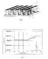
- FIG. 4is a graph showing change in read current for a memory cell of the present invention as voltage in reverse bias across the diode increases.
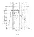
- FIG. 5is a probability plot showing memory cells transformed from the V state to the P state, from the P state to the R state, and from the R state to the S state.
- FIG. 6is a probability plot showing memory cells transformed from the V state to the P state, from the P state to the S state, and from the S state to the R state.
- FIG. 7is a probability plot showing memory cells transformed from the V state to the R state, from the R state to the S state, and from the S state to the P state.
- FIG. 8is a perspective view of a vertically oriented p-i-n diode that may be used in embodiments of the present invention.
- FIG. 9is a probability plot showing memory cells transformed from the V state to the P state, and from the P state to the M state.
- FIG. 10is a perspective view of a multi-state or rewriteable memory cell formed according to a preferred embodiment of the present invention.
- FIG. 11is a probability plot showing memory cells transformed from the V state to the P state, from the P state to the R state, and from the R state to the S state, then repeatably between the S state and the R state.
- FIG. 12is a circuit diagram showing a biasing scheme to bias the S cell in forward bias.
- FIG. 13is a circuit diagram showing one biasing scheme to bias the S cell in reverse bias.
- FIG. 14illustrates iterative read-verify-write cycles to move a cell into a data state.
- FIGS. 15 a - 15 care cross-sectional views illustrating stages in formation of a memory level formed according to an embodiment of the present invention.
- FIG. 16is cross-sectional view illustrating a diode and resistive switching element that may be used an alternative embodiment of the present invention.
- FIG. 17is an illustration of a mixed-use memory array of a preferred embodiment in which a first set of memory cells operate as one-time programmable memory cells and a second set of memory cells operate as rewritable memory cells.
- FIG. 18is an illustration of a mixed-use memory array of a preferred embodiment in which multiple sets of one-time programmable and rewritable memory cells are interleaved.
- FIG. 19is an illustration of a circuit of a preferred embodiment showing a set of memory cells that are programmed with forward bias.
- FIG. 20is an illustration of a circuit of a preferred embodiment showing a set of memory cells that are programmed with reverse bias.
- FIG. 21is an illustration of a memory array of a preferred embodiment in which a first portion of the memory array stores two data states per memory cell and a second portion of the memory array stores four data states per memory cell.
- FIG. 22is an illustration of a memory array of a preferred embodiment in which two-state-per-cell portions and four-state-per-cell portions are indicated by flag bits on each physical page.
- FIG. 23is an illustration of a memory array of a preferred embodiment in which two-state-per-cell portions and four-state-per-cell portions are indicated by a translation table stored in the memory array.
- FIG. 24is an illustration of a memory array of a preferred embodiment in which a two-state-per-cell one-time programmable portion, a two-state-per-cell rewritable portion, and a four-state-per-cell one-time programmable portion are indicated by flag bits on each physical page.
- FIG. 25is a flow chart of a preferred embodiment for using chip flags and an off-chip bad block mechanism.
- trimmable resistorshave been used as elements in integrated circuits.
- Leakage currentcan be greatly reduced by forming each memory cell as a two-terminal device including a diode.
- a diodehas a non-linear I-V characteristic, allowing very little current flow below a turn-on voltage, and substantially higher current flow above the turn-on voltage.
- a diodealso acts as one-way valves passing current more easily in one direction than the other.
- a memory element formed of doped semiconductor materialfor example the semiconductor diode of the '549 application, can achieve three, four, or more stable resistivity states.
- semiconductor materialcan be converted from an initial high-resistivity state to a lower-resistivity state; then, upon application of an appropriate electrical pulse, can be returned to a higher-resistivity state.
- These embodimentscan be employed independently or combined to form a memory cell which can have two or more data states, and can be one-time-programmable or rewriteable.
- a diode between conductors in the memory cellallows its formation in a highly dense cross-point memory array.
- a polycrystalline, amorphous, or microcrystalline semiconductor memory elementeither is formed in series with a diode or, more preferably, is formed as the diode itself.
- transition from a higher- to a lower-resistivity statewill be called a set transition, affected by a set current, a set voltage, or a set pulse; while the reverse transition, from a lower- to a higher-resistivity state, will be called a reset transition, affected by a reset current, a reset voltage, or a reset pulse.
- a polycrystalline semiconductor diodeis paired with a dielectric rupture antifuse, though in other embodiments the antifuse may be omitted.
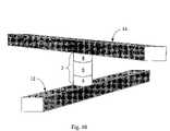
- FIG. 2illustrates a memory cell formed according to a preferred embodiment of the present invention.
- a bottom conductor 12is formed of a conductive material, for example tungsten, and extends in a first direction. Barrier and adhesion layers may be included in bottom conductor 12 .
- Polycrystalline semiconductor diode 2has a bottom heavily doped n-type region 4 ; an intrinsic region 6 , which is not intentionally doped; and a top heavily doped region 8 , though the orientation of this diode may be reversed. Such a diode, regardless of its orientation, will be referred to as a p-i-n diode.
- Dielectric rupture antifuse 14is included in some embodiments.
- Top conductor 16may be formed in the same manner and of the same materials as bottom conductor 12 , and extends in a second direction different from the first direction.
- Polycrystalline semiconductor diode 2is vertically disposed between bottom conductor 12 and top conductor 16 .
- Polycrystalline semiconductor diode 2is formed in a high-resistivity state.
- This memory cellcan be formed above a suitable substrate, for example above a monocrystalline silicon wafer.
- FIG. 3shows a portion of a memory level of such devices formed in a cross-point array, where diodes 2 are disposed between bottom conductors 12 and top conductors 16 (antifuses 14 are omitted in this view.)
- Multiple memory levelscan be stacked over a substrate to form a highly dense monolithic three dimensional memory array.
- an intrinsic regionmay in fact include a low concentration of p-type or n-type dopants. Dopants may diffuse into the intrinsic region from adjacent regions, or may be present in the deposition chamber during deposition due to contamination from an earlier deposition. It will further be understood that deposited intrinsic semiconductor material (such as silicon) may include defects which cause it to behave as if slightly n-doped. Use of the term “intrinsic” to describe silicon, germanium, a silicon-germanium alloy, or some other semiconductor material is not meant to imply that this region contains no dopants whatsoever, nor that such a region is perfectly electrically neutral.
- the resistivity of doped polycrystalline or microcrystalline semiconductor materialcan be changed between stable states by applying appropriate electrical pulses. It has been found that in preferred embodiments, set transitions are advantageously performed with the diode under forward bias, while reset transitions are most readily achieved and controlled with the diode under reverse bias. In some instances, however, set transitions may be achieved with the diode under reverse bias, while reset transitions are achieved with the diode under forward bias.
- Switching under reverse biasshows a distinct behavior.
- a polysilicon p-i-n diode like the one shown in FIG. 2is subjected to a relatively large switching pulse under reverse bias.
- a smaller read pulsefor example 2 volts
- the read currentis measured.
- the subsequent read currentat two volts changes as shown in FIG. 4 . It will be seen that initially as the reverse voltage and current of the switching pulse are increased, the read current, when a read voltage is applied after each switching pulse, increases; i.e.
- the initial transition of the semiconductor material(silicon, in this case) is in the set direction toward lower resistivity.
- the switching pulsereaches a certain reverse bias voltage, at point K in FIG. 4 , about ⁇ 14.6 volts in this example, the read current abruptly begins to drop as reset is achieved and resistivity of the silicon increases.
- the switching voltage at which the set trend is reversed and the silicon of the diode begins to resetvaries, depending on, for example, the resistivity state of the silicon making up the diode when application of the reverse bias switching pulse is begun. It will be seen, then, that by selecting appropriate voltages, either set or reset of the semiconductor material making up the diode can be achieved with the diode under reverse bias.
- Distinct data states of the memory cell of the present inventioncorrespond to resistivity states of polycrystalline or microcrystalline semiconductor material making up the diode, which are distinguished by detecting current flow through the memory cell (between top conductor 16 and bottom conductor 12 ) when a read voltage is applied.
- the current flowing between any one distinct data state and any different distinct data stateis at least a factor of two, to allow the difference between the states to be readily detectable.
- the memory cellcan be used as a one-time programmable cell or a rewriteable memory cell, and may have two, three, four, or more distinct data states.
- the cellcan be converted from any of its data states to any other of its data states in any order, and under either forward or reverse bias.
- a diode formed of polycrystalline semiconductor material and a dielectric rupture antifuseare arranged in series disposed between a top and bottom conductor.
- the two-terminal deviceis used as a one-time-programmable multilevel cell, in preferred embodiments having three or four distinct data states.
- Diode 2is preferably formed of a polycrystalline or microcrystalline semiconductor material, for example silicon, germanium, or an alloy of silicon and/or germanium. Diode 2 is most preferably polysilicon. In this example, bottom heavily doped region 4 is n-type and top heavily doped region 8 is p-type, though the polarity of the diode may be reversed.
- the memory cellcomprises a portion of the top conductor, a portion of the bottom conductor, and a diode, the diode disposed between the conductors.
- FIG. 5is a probability plot showing current of a memory cells in various states.
- a read voltagefor example 2 volts
- the read current flowing between top conductor 16 and bottom conductor 12is preferably in the range of nanoamps, for example less than about about 5 nanoamps.
- Area V on the graph of FIG. 5corresponds to a first data state of the memory cell. For some memory cells in the array, this cell will not be subjected to set or reset pulses, and this state will be read as a data state of the memory cell. This first data state will be referred to as the V state.
- a first electrical pulsepreferably with diode 2 under forward bias, is applied between top conductor 16 and bottom conductor 12 .
- This pulseis, for example, between about 8 volts and about 12 volts, for example about 10 volts.
- the currentis, for example, between about 80 and about 200 microamps.
- the pulse widthis preferably between about 100 and about 500 nsec.
- This first electrical pulseruptures dielectric rupture antifuse 14 and switches the semiconductor material of diode 2 from a first resistivity state to a second resistivity state, the second state lower resistivity than the first.
- This second data statewill be referred to as the P state, and this transition is labeled “V ⁇ P” in FIG. 5 .
- the current flowing between top conductor 16 and bottom conductor 12 at a read voltage of 2 voltsis about 10 microamps or more.
- the resistivity of the semiconductor material making up diode 2is reduced by a factor of about 1000 to about 2000. In other embodiments the change in resistivity will be less, but between any data state and any other data state will be at least a factor of two, preferably at least a factor of three or five, and more typically a factor of 100 or more. Some memory cells in the array will be read at this data state, and will not be subjected to additional set or reset pulses. This second data state will be referred to as the P state.
- a second electrical pulsepreferably with diode 2 under reverse bias, is applied between top conductor 16 and bottom conductor 12 .
- This pulseis, for example, between about ⁇ 8 volts and about ⁇ 14 volts, preferably about between about ⁇ 10 and about ⁇ 12 volts, preferably about ⁇ 11 volts.
- the currentis, for example, between about 80 and about 200 microamps.
- the pulse widthis, for example, between about 100 nanosec and about 10 microseconds; preferably between about 100 nsec and about 1 microsecond, most preferably between about 200 and about 800 nsec.
- This second electrical pulseswitches the semiconductor material of diode 2 from the second resistivity state to a third resistivity state, the third resistivity state higher resistivity than the second.
- the current flowing between top conductor 16 and bottom conductor 12 at a read voltage of 2 voltsis between about 10 and about 500 nanoamps, preferably between about 100 and about 500 nanoamps. Some memory cells in the array will be read at this data state, and will not be subjected to additional set or reset pulses.
- This third data statewill be referred to as the R state, and this transition is labeled “P ⁇ R” in FIG. 5 .
- a third electrical pulsepreferably with diode 2 under forward bias, is applied between top conductor 16 and bottom conductor 12 .
- This pulseis, for example, between about 8 volts and about 12 volts, for example about 10 volts, with current between about 5 and about 20 microamps.
- This third electrical pulseswitches the semiconductor material of diode 2 from the third resistivity state to a fourth resistivity state, the fourth resistivity state lower resistivity than the third, and preferably higher resistivity than the second resistivity state.
- the current flowing between top conductor 16 and bottom conductor 12 at a read voltage of 2 voltsis between about 1.5 and about 4.5 microamps.
- the difference in current at the read voltageis preferably at least a factor of two between any two adjacent data states.
- the read current of any cell in data state Ris preferably at least two times that of any cell in data state V
- the read current of any cell in data state Sis preferably at least two times that of any cell in data state R
- the read current of a cell in data state Pis preferably at least two times that of any cell in data state S.
- the read current at data state Rmay be two times the read current at data state V
- the read current at data state Smay be two times the read current at data state R
- the read current at data state Pmay be two times the read current at data state S.
- the differencecould be considerably larger; for example, if the highest-current V state cell can have a read current of 5 nanoamps and the lowest-current R state call can have a read current of 100 nanoamps, the difference in current is at least a factor of 20. By selecting other limits, it can be assured that the difference in read current between adjacent memory states will be at least a factor of three.
- an iterative read-verify-write processmay be applied to assure that a memory cell is in one of the defined data states after a set or reset pulse, and not between them.
- a memory cell having four distinct data stateshas been described. To aid in distinguishing between the data states, it may be preferred for three rather than four data states to be selected.
- a three-state memory cellcan be formed in data state V, set to data state P, then reset to data state R. This cell will have no fourth data state S.
- the difference between adjacent data statesfor example between the R and P data states, can be significantly larger.
- the cellsmay be programmed in a variety of ways, however.
- the memory cell of FIG. 2may be formed in a first state, the V state.
- a first electrical pulsepreferably under forward bias, ruptures antifuse 14 and switches the polysilicon of the diode from a first resistivity state to a second resistivity state lower than the first, placing the memory cell in the P state, which in this example is the lowest resistivity state.
- a second electrical pulsepreferably under reverse bias, switches the polysilicon of the diode from the second resistivity state to a third resistivity state, the third resistivity state higher resistivity than the second, placing the memory cell in the S state.
- a third electrical pulsepreferably also under reverse bias, switches the polysilicon of the diode from the third resistivity state to a fourth resistivity state, the third resistivity state higher resistivity than the second, placing the memory cell in the R state.
- any of the data states, the V state, the R state, the S state, and the P statecan be read as a data state of the memory cell.
- Each transitionis labeled in FIG. 6 . Four distinct states are shown; there could be three or more than four states as desired.
- each successive electrical pulsecan switch the semiconductor material of the diode to a successively lower resistivity state.
- the memory cellcan proceed from the initial V state to the R state, from the R state to the S state, and from the S state to the P state, where for each state the read current is at least two times the read current at the previous state, each corresponding to a distinct data state.
- This schememay be most advantageous when there is no antifuse included in the cell.
- the pulsesmay be applied under either forward or reverse bias. In alternative embodiments there may be three data states or more than four data states.
- a memory cellincludes the polysilicon or microcrystalline diode 2 shown in FIG. 8 , including bottom heavily doped p-type region 4 , middle intrinsic or lightly doped region 6 , and top heavily doped n-type region 8 .
- this diode 2can be arranged in series with a dielectric rupture antifuse, the two disposed between top and bottom conductors.
- Bottom heavily doped p-type region 4may be in situ doped, i.e. doped by flowing a gas that provides a p-type dopant such as boron during deposition of the polysilicon, such that dopant atoms are incorporated into the film as it forms.
- this memory cellis formed in the V state, where the current between top conductor 16 and bottom conductor 12 is less than about 80 nanoamps at a read voltage of 2 volts.
- a first electrical pulsepreferably applied under forward bias of, for example, about 8 volts, ruptures dielectric rupture antifuse 14 , if it is present, and switches the polysilicon of diode 2 from a first resistivity state to a second resistivity state, the second resistivity state lower than the first, placing the memory cell in data state P.
- data state Pthe current between top conductor 16 and bottom conductor 12 at the read voltage is between about 1 microamp and about 4 microamps.
- a second electrical pulsepreferably applied in reverse bias, switches the polysilicon of diode 2 from the second resistivity state to a third resistivity state, the third resistivity state lower than the first.
- the third resistivity statecorresponds to data state M.
- data state Mthe current between top conductor 16 and bottom conductor 12 at the read voltage is above about 10 microamps.
- the difference in current between any cell in adjacent data statesis preferably at least a factor of two, preferably a factor of three or more. Any of the data states V, P, or M can be detected as a data state of the memory cell.
- FIG. 4showed that when a semiconductor diode is subjected to reverse bias, in general the semiconductor material initially undergoes a set transition to lower resistivity, then, as voltage is increased, undergoes a reset transition to higher resistivity.
- the switch from set transition to reset transition with increasing reverse bias voltagedoes not occur as abruptly or as steeply as with other embodiments of the diode. This means a set transition under reverse bias is easier to control with such a diode.
- the memory cellbehaves as a rewriteable memory cell, which is repeatably switchable between two or between three data states.
- FIG. 10shows a memory cell that may serve as a rewriteable memory cell. This memory cell is the same as the one shown in FIG. 2 , except no dielectric rupture antifuse is included. Most rewriteable embodiments do not include an antifuse in the memory cell, though one may be included if desired.
- the memory cellis formed in a high resistivity state V, with current at 2 volts about 5 nanoamps or less.
- Vhigh resistivity state
- the initial V statedoes not serve as a data state of the memory cell.
- a first electrical pulsepreferably with diode 2 under forward bias, is applied between top conductor 16 and bottom conductor 12 . This pulse is, for example, between about 8 and about 12 volts, preferably about 10 volts. This first electrical pulse switches the semiconductor material of diode 2 from a first resistivity state to a second resistivity state P, the second state lower resistivity than the first.
- the P statealso will not serve as a data state of the memory cell. In other embodiments, the P state will serve as a data state of the memory cell.
- a second electrical pulsepreferably with diode 2 under reverse bias, is applied between top conductor 16 and bottom conductor 12 .
- This pulseis, for example, between about ⁇ 8 and about ⁇ 14 volts, preferably between about ⁇ 9 and about ⁇ 13 volts, more preferably about ⁇ 10 or ⁇ 11 volts.
- the voltage requiredwill vary with the thickness of the intrinsic region.
- This second electrical pulseswitches the semiconductor material of diode 2 from the second resistivity state to a third resistivity state R, the third state higher resistivity than the second.
- the R statecorresponds to a data state of the memory cell.
- a third electrical pulsecan be applied between top conductor 16 and bottom conductor 12 , preferably under forward bias.
- This pulseis, for example, between about 5.5 and about 9 volts, preferably about 6.5 volts, with current between about 10 and about 200 microamps, preferably between about 50 and about 100 microamps.
- This third electrical pulseswitches the semiconductor material of diode 2 from the third resistivity state R to a fourth resistivity state S, the fourth state lower resistivity than the third.
- the S statecorresponds to a data state of the memory cell.
- the R state and the S stateare sensed, or read, as data states.
- the memory cellcan repeatedly be switched between these two states. For example, a fourth electrical pulse, preferably with diode 2 under reverse bias, switches the semiconductor material of the diode from the fourth resistivity state S to the fifth resistivity state R, which is substantially the same as the third resistivity state R.
- a fifth electrical pulsepreferably with diode 2 under forward bias, switches the semiconductor material of the diode from the fifth resistivity state R to the sixth resistivity state S, which is substantially the same as the fourth resistivity state S, and so on.
- both the first electrical pulse, which switches the cell from the initial V state to the P state, and the second electrical pulse, which switches the cell from the P state to the R state,may be performed before the memory array reaches the end user, for example in a factory or test facility, or by a distributor before sale.
- the difference between current flow under read voltage, for example of 2 volts, between top conductor 16 and bottom conductor 12 between any cell in one data state and any cell in an adjacent data states, in this case the R data state (between about 10 and about 500 nanoamps) and the S data state (between about 1.5 and about 4.5 microamps),is at least a factor of three.
- the differencemay be a factor of two, three, five, or more.
- a rewriteable memory cellcan be switched between three or more data states, in any order. Either set or reset transitions can be performed with the diode under either forward or reverse bias.
- the data statecorresponds to the resistivity state of polycrystalline or microcrystalline semiconductor material making up a diode.
- the data statesdoes not correspond to the resistivity state of a resistivity-switching metal oxide or nitride, as in Herner et al., U.S. patent application Ser. No. 11/395,995, “Nonvolatile Memory Cell Comprising a Diode and a Resistance-Switching Material,” filed Mar. 31, 2006, owned by the assignee of the present invention and hereby incorporated by reference.
- any step in which cells are subjected to large voltages in reverse biashas reduced leakage current as compared to a forward bias step.
- Bitline B 0is set at 10 volts and wordline W 0 is set at ground.
- wordline W 1is set less than but relatively close to the voltage of bitline B 0 ; for example wordline W 1 may be set to 9.3 volts, so that 0.7 volts is applied across the F cells (only one F cell is shown, but there may be hundreds, thousands or more.)
- bitline B 1is set higher than but relatively close to the voltage of wordline W 0 ; for example bitline B 1 may be set to 0.7 volts, so that 0.7 volts is applied across cell H (again, there may be thousands of H cells.)
- the unselected cells Uwhich share neither wordline W 0 or bitline B 0 with selected cell S, are subjected to ⁇ 8.6 volts. As there may be millions of unselected cells U
- FIG. 13shows an advantageous biasing scheme to apply a large reverse bias across a memory cell, for example as a reset pulse.
- Bitline B 0is set at ⁇ 5 volts and wordline W 0 at 5 volts, so that ⁇ 10 volts is applied across selected cell S; the diode is in reverse bias.
- Setting wordline W 1 and bitline B 1 at groundsubjects both half-selected cells F and H to ⁇ 5 volts, at a reverse bias low enough not to cause unintentional set or reset of these cells.
- Set or reset in reverse biasgenerally seems to take place at or near the voltage at which the diode goes into reverse breakdown, which is generally higher than ⁇ 5 volts.
- bitline B 0can be set at 0 volts, wordline W 0 at ⁇ 10 volts, and bitline B 1 and wordline W 1 at ⁇ 5 volts.
- the voltage across selected cell S, half-selected cells H and F, and unselected cells Uwill be the same as in the scheme of FIG. 13 .
- bitline B 0is set at ground, wordline W 0 at 10 volts, and bitline B 1 and wordline W 1 each at 5 volts.
- the difference between current flow during read in adjacent data statesis preferably at least a factor of two; in many embodiments, it may be preferred to establish current ranges for each data state which are separated by a factor of three, five, ten, or more.
- data state Vmay be defined as read current of 5 nanoamps or less at a read voltage of 2 volts, data state R as read current between about 10 and about 500 nanoamps, data state S as read current between about 1.5 and about 4.5 microamps, and data state P as read current above about 10 microamps.
- data state Vmay be defined in a smaller range, with read current about 5 nanoamps or less at a read voltage of 2 volts. Actual read currents will vary with characteristics of the cell, construction of the array, read voltage selected, and many other factors.
- a one-time programmable memory cellis in data state P.
- An electrical pulse in reverse biasis applied to the memory cell to switch the cell into data state S.
- the read currentis not in the desired range; i.e. the resistivity state of the semiconductor material of the diode is higher or lower than intended.
- the read current of the memory cellis at the point on the graph shown at Q, in between the S state and P state current ranges.
- the memory cellmay be read to determine if the desired data state was reached. If the desired data state was not reached, an additional pulse is applied. For example, when the current Q is sensed, an additional reset pulse is applied to increase the resistivity of the semiconductor material, decreasing the read current into the range corresponding to the S data state. As described earlier, this set pulse may be applied in either forward or reverse bias. The additional pulse or pulses may have a higher amplitude (voltage or current) or longer or shorter pulse width than the original pulse. After the additional set pulse, the cell is read again, then set or reset pulses applied as appropriate until the read current is in the desired range.
- a two-terminal devicesuch as the memory cell including a diode described
- Applying a large reverse bias across the diodemay damage the diode; thus when performing a set or reset with the diode under reverse bias, it is advantageous to minimize the reverse bias voltage.
- an amorphous or microcrystalline silicon materialis crystallized not in contact with a silicon having a silicide with which it has a good lattice match, for example in contact only with materials such as silicon dioxide and titanium nitride, with which it has a significant lattice mismatch, the resulting polysilicon will have many more defects, and doped polysilicon crystallized this way will be much less conductive as formed.
- the semiconductor material forming a diodeis switched between two or more resistivity states, changing the current flowing through the diode at a given read voltage, the different currents (and resistivity states) corresponding to distinct data states. It has been found that diodes formed of high-defect silicon (or other appropriate semiconductor materials such as germanium or silicon-germanium alloys) which has not been crystallized adjacent to a silicide or analogous material providing a crystallization template exhibit the most advantageous switching behavior.
- the resistivity state of very low-defect silicon crystallized adjacent to an appropriate silicidecannot be switched as readily as when the semiconductor material has a higher level of defects. It may be that the presence of defects, or of a larger number of grain boundaries, allows for easier switching.
- the polycrystalline or microcrystalline material forming the diodeis not crystallized adjacent to a material with which it has a small lattice mismatch.
- a small lattice mismatchis, for example, a lattice mismatch of about three percent or less.
- switching behaviormay be centered on changes in the intrinsic region. Switching behavior has been observed in resistors and p-n diodes as well, and is not limited to p-i-n diodes, but it is believed that the use of p-i-n diodes may be particularly advantageous.
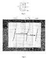
- Fabrication of a single memory levelwill be described in detail. Additional memory levels can be stacked, each monolithically formed above the one below it. In this embodiment, a polycrystalline semiconductor diode will serve as the switchable memory element.
- This substrate 100can be any semiconducting substrate as known in the art, such as monocrystalline silicon, IV-IV compounds like silicon-germanium or silicon-germanium-carbon, III-V compounds, II-VII compounds, epitaxial layers over such substrates, or any other semiconducting material.
- the substratemay include integrated circuits fabricated therein.
- the insulating layer 102is formed over substrate 100 .
- the insulating layer 102can be silicon oxide, silicon nitride, high-dielectric film, Si—C—O—H film, or any other suitable insulating material.
- the first conductors 200are formed over the substrate and insulator.
- An adhesion layer 104may be included between the insulating layer 102 and the conducting layer 106 to help conducting layer 106 adhere to insulating layer 102 . If the overlying conducting layer is tungsten, titanium nitride is preferred as adhesion layer 104 .
- Conducting layer 106can comprise any conducting material known in the art, such as tungsten, or other materials, including tantalum, titanium, copper, cobalt, or alloys thereof.
- the layerswill be patterned and etched using any suitable masking and etching process to form substantially parallel, substantially coplanar conductors 200 , shown in FIG. 15 a in cross-section.
- photoresistis deposited, patterned by photolithography and the layers etched, and then the photoresist removed using standard process techniques.
- Conductors 200could be formed by a Damascene method instead.
- Dielectric material 108is deposited over and between conductor rails 200 .
- Dielectric material 108can be any known electrically insulating material, such as silicon oxide, silicon nitride, or silicon oxynitride. In a preferred embodiment, silicon dioxide is used as dielectric material 108 .
- FIG. 15 aThis removal of dielectric overfill to form planar surface 109 can be performed by any process known in the art, such as chemical mechanical planarization (CMP) or etchback.
- CMPchemical mechanical planarization
- An etchback technique that may advantageously be usedis described in Raghuram et al., U.S. application Ser. No. 10/883,417, “Nonselective Unpatterned Etchback to Expose Buried Patterned Features,” filed Jun. 30, 2004 and hereby incorporated by reference.
- a plurality of substantially parallel first conductorshave been formed at a first height above substrate 100 .
- a barrier layer 110is deposited as the first layer after planarization of the conductor rails.
- Any suitable materialcan be used in the barrier layer, including tungsten nitride, tantalum nitride, titanium nitride, or combinations of these materials.
- titanium nitrideis used as the barrier layer.
- the barrier layeris titanium nitride, it can be deposited in the same manner as the adhesion layer described earlier.
- the semiconductor materialcan be silicon, germanium, a silicon-germanium alloy, or other suitable semiconductors, or semiconductor alloys.
- silicongermanium
- a silicon-germanium alloyor other suitable semiconductors, or semiconductor alloys.
- this descriptionwill refer to the semiconductor material as silicon, but it will be understood that the skilled practitioner may select any of these other suitable materials instead.
- the pillarcomprises a semiconductor junction diode.
- junction diodeis used herein to refer to a semiconductor device with the property of non-ohmic conduction, having two terminal electrodes, and made of semiconducting material which is p-type at one electrode and n-type at the other. Examples include p-n diodes and n-p diodes, which have p-type semiconductor material and n-type semiconductor material in contact, such as Zener diodes, and p-i-n diodes, in which intrinsic (undoped) semiconductor material is interposed between p-type semiconductor material and n-type semiconductor material.
- Bottom heavily doped region 112can be formed by any deposition and doping method known in the art.
- the siliconcan be deposited and then doped, but is preferably doped in situ by flowing a donor gas providing n-type dopant atoms, for example phosphorus, during deposition of the silicon.
- Heavily doped region 112is preferably between about 100 and about 800 angstroms thick.
- Intrinsic layer 114can be formed by any method known in the art.
- Layer 114can be silicon, germanium, or any alloy of silicon or germanium and has a thickness between about 1100 and about 3300 angstroms, preferably about 2000 angstroms.
- Pillars 300should have about the same pitch and about the same width as conductors 200 below, such that each pillar 300 is formed on top of a conductor 200 . Some misalignment can be tolerated.
- the pillars 300can be formed using any suitable masking and etching process.
- photoresistcan be deposited, patterned using standard photolithography techniques, and etched, then the photoresist removed.
- a hard mask of some other materialfor example silicon dioxide, can be formed on top of the semiconductor layer stack, with bottom antireflective coating (BARC) on top, then patterned and etched.
- BARCbottom antireflective coating
- DARCdielectric antireflective coating
- Dielectric material 108is deposited over and between the semiconductor pillars 300 , filling the gaps between them.
- Dielectric material 108can be any known electrically insulating material, such as silicon oxide, silicon nitride, or silicon oxynitride. In a preferred embodiment, silicon dioxide is used as the insulating material.
- dielectric material on top of the pillars 300is removed, exposing the tops of pillars 300 separated by dielectric material 108 , and leaving a substantially planar surface.
- This removal of dielectric overfillcan be performed by any process known in the art, such as CMP or etchback.
- CMP or etchbackion implantation is performed, forming heavily doped p-type top region 116 .
- the p-type dopantis preferably boron or BCl 3 .
- This implant stepcompletes formation of diodes 111 .
- the resulting structureis shown in FIG. 15 b . In the diodes just formed, bottom heavily doped regions 112 are n-type while top heavily doped regions 116 are p-type; clearly the polarity could be reversed.
- next dielectric rupture antifuse layer 118is formed on top of each heavily doped region 116 .
- Antifuse 118is preferably a silicon dioxide layer formed by oxidizing the underlying silicon in a rapid thermal anneal, for example at about 600 degrees.
- Antifuse 118may be about 20 angstroms thick. Alternatively, antifuse 118 can be deposited.
- Top conductors 400can be formed in the same manner as bottom conductors 200 , for example by depositing adhesion layer 120 , preferably of titanium nitride, and conductive layer 122 , preferably of tungsten. Conductive layer 122 and adhesion layer 120 are then patterned and etched using any suitable masking and etching technique to form substantially parallel, substantially coplanar conductors 400 , shown in FIG. 15 c extending left-to-right across the page. In a preferred embodiment, photoresist is deposited, patterned by photolithography and the layers etched, and then the photoresist removed using standard process techniques.
- the dielectric materialcan be any known electrically insulating material, such as silicon oxide, silicon nitride, or silicon oxynitride. In a preferred embodiment, silicon oxide is used as this dielectric material.
- Formation of a first memory levelhas been described. Additional memory levels can be formed above this first memory level to form a monolithic three dimensional memory array.
- conductorscan be shared between memory levels; i.e. top conductor 400 would serve as the bottom conductor of the next memory level.
- an interlevel dielectric(not shown) is formed above the first memory level of FIG. 15 c , its surface planarized, and construction of a second memory level begins on this planarized interlevel dielectric, with no shared conductors.
- a monolithic three dimensional memory arrayis one in which multiple memory levels are formed above a single substrate, such as a wafer, with no intervening substrates.
- the layers forming one memory levelare deposited or grown directly over the layers of an existing level or levels.
- stacked memorieshave been constructed by forming memory levels on separate substrates and adhering the memory levels atop each other, as in Leedy, U.S. Pat. No. 5,915,167, “Three dimensional structure memory.”
- the substratesmay be thinned or removed from the memory levels before bonding, but as the memory levels are initially formed over separate substrates, such memories are not true monolithic three dimensional memory arrays.
- a monolithic three dimensional memory array formed above a substratecomprises at least a first memory level formed at a first height above the substrate and a second memory level formed at a second height different from the first height. Three, four, eight, or indeed any number of memory levels can be formed above the substrate in such a multilevel array.
- FIG. 16shows a switchable memory element 117 formed in series with a diode 111 .
- the switchable memory element 117is formed of semiconductor material which is switched between resistivity states using electrical pulses as described.
- the diodeis preferably crystallized adjacent to a silicide such as cobalt silicide, which provides a crystallization template, as described earlier, such that the semiconductor material of the diode is very low-defect and exhibits little or no switching behavior.
- Switchable memory element 117is preferably doped, and should be doped to the same conductivity type as top heavily doped region 116 . Methods to fabricate this device are described in the '167 application.
- the above embodimentsdescribe how a single memory cell can be used as a two-data-state memory cell, a more-than-two-data-state memory cell, a one-time programmable memory cell, or a rewritable memory cell.
- This versatilityallows a common memory cell architecture to be used to provide multiple types of memory products. The following is a discussion of the multi-use nature of the memory cell and its potential to provide a mixed-use memory array.
- the memory cell described abovehas a memory element comprising a switchable resistance material, such as a semiconductor material, that is configurable to one of at least three resistivity states.
- a memory elementcan be “configured” to a resistivity state during the formation of the memory element (e.g., the initial, unprogrammed state of a memory element has an initial resistivity state) or by subsequently subjecting the memory element to set or reset pulses. Because of this characteristic, a single memory cell can act in two different ways: as a one-time programmable memory cell or a rewritable memory cell. Also because of this characteristic, a single memory cell can use two data states or more than two data states. Accordingly, any given manufactured memory cell has the potential of being operable as a one-time programmable memory cell or a rewritable memory cell with two or more data states.
- resistivity statethat is used to represent a data state of a memory cell when the memory cell operates as a one-time programmable memory cell but not when the memory cell operates as a rewritable memory cell.
- the memory cellis manufactured in an initial resistivity state (the V state), and this resistivity state is used when the memory cell operates as a one-time programmable memory cell but not when the memory cell operates as a rewritable memory cell.
- R and S statesTwo other data states (the R and S states) are used to represent data states of the memory cell when the memory cell operates as a rewritable memory cell. (As described below, these data states can also be used in a one-time programmable memory cell.) These data states are achieved by varying the resistance of the switchable resistance material. Again, these other data states do not include the data state that is only used to represent a data state when the memory cell operates as a one-time programmable memory cell. Additional data state(s) (e.g., an “R2” data state between the R state and the S state) can be used to allow a rewritable memory cell to achieve three or more respective data states.
- R2data state between the R state and the S state
- the memory elementcomprises a switchable resistance material (e.g., a semiconductor material) in series with an antifuse
- the V stateis the resistivity state used only when the memory cell operates as a one-time programmable memory cell. This is because, once the antifuse is blown, the memory element cannot go back to the V state.
- one resistivity statecan be designated as the state that is only used when the memory cell operates as a one-time programmable memory cell.
- the P statecan also be a resistivity state that is used when the memory cell operates as a one-time programmable memory cell but not when the memory cell operates as a rewritable memory cell.
- one or both of the R and S statesare used to represent a data state of a one-time programmable memory cell, such as when the one-time programmable memory cell stores three or four data states. In such a situation, the one-time programmable and rewritable uses of the memory cell would have a resistivity state in common.
- a one-time programmable memory cellcan have one state in common with a rewritable memory cell (e.g., where there is no distinction between the S state and the P state). Nevertheless, there would still be at least one resistivity state (e.g., the V state) that would be used to represent a data state of the memory cell when the memory cell operates as a one-time programmable memory cell but not when the memory cell operates as a rewritable memory cell.
- One advantage of this versatilityis that a single integrated circuit with such memory cells can be designated either as a one-time programmable memory array or as a rewritable memory array. This provides flexibility in manufacturing and yield enhancement.
- a set of test memory cellse.g., test rows and columns
- the test memory cellscan be exercised by repeatedly programming, reseting, and setting the memory cells.
- the partwill probably not program correctly as a rewritable memory array.
- the cells in the memory arraycan operate as either one-time programmable memory cells or rewritable memory cells, instead of discarding the part because it did not provide the expected rewritable yield, the part can be designated as a one-time programmable memory array. Accordingly, the common backbone architecture of the memory cells provides flexibility in manufacturing and yield enhancement.
- Memory arrays passing the testcan go on to further formatting (e.g., all the memory cells being programmed from the V state to the P state, then exercised between the R and S states as a final qualification test) and then shipping to a store or end user as a rewritable memory array (e.g., a memory card for a digital camera).
- Memory arrays failing the testcan be packaged and sent to a different part of the factory for programming one-time programmable content. Alternatively, the part can be sent to a store, with a store employee or end user field programming one-time programmable content (e.g., using a kiosk). The unprogrammed part can also be sold to the end user for use as archival memory.
- a flagbe used to signal a device that reads and writes to the memory array (e.g., a controller on the memory device that includes the memory array or hardware/software in a host device) that the memory array is one-time programmable or rewritable.
- the “flag”can be one or more bits stored in the memory array.
- a flagcan be set in a special address location in the memory array (e.g., address 0000). When the host device detects the flag, it can adapt to the one-time programmable nature of the memory array by not attempting to reprogram it.
- the memory arraycan be a “mixed-use” memory array. Since every single memory cell in the array can act either as a one-time programmable memory cell or as a rewritable memory cell, in this embodiment, a first set of memory cells operates as one-time programmable memory cells and a second, different set of memory cells operates as rewritable memory cells. In this way, one-time programmable memory cells and rewritable memory cells can be provided on the same integrated circuit. As above, testing can be performed to determine whether a given set of memory cells should be designated as one-time programmable memory cells or rewritable memory cells.
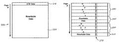
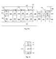
- FIG. 17is an illustration of a mixed use array 200 of a preferred embodiment.
- a first set of memory cells 210operates as one-time programmable memory cells and a second, different set of memory cells 220 operates as rewritable memory cells.
- the memory cells in both sets 210 , 220contain the same number of data states per cell, although variations in the number of data states per memory cell are possible, as described below.
- the first set of memory cellsstores data that is considered permanent and can relate to the operation of the memory array. Examples of such information includes, but is not limited to, one or more of the following: content management bits, trim bits, manufacturer data, and format data.
- “Content management bits”refers to information that relates to the management of programmed content.
- “Trim bits”are customized information that set various options in on-chip circuitry. In operation, the on-chip circuitry reads the trim bits in the first set of memory cells 210 , and the read trim bits control the further operation of the circuitry. For example, the trim bits could contain a setting for the preferred write/read value (current or voltage) of the write/read circuitry of the memory device.
- “Manufacturer data”can include the manufacturer's name and serial number.
- “Format data”indicates bad portions of the memory array; specifically, that a particular row and/or column in the memory array is bad and the location of a redundant row and/or column. Further information regarding redundancy can be found in U.S.
- the first set of memory cells 210can contain game content data (i.e., computer program code for a game), and the second set of memory cells 220 can contain game state data (i.e., an indication of the user's location in the game when the user requests that the game be saved).
- game content datai.e., computer program code for a game
- game state datai.e., an indication of the user's location in the game when the user requests that the game be saved.
- the data in either the first or second sets 210 , 220can be programmed at the factory or by a subsequent user.
- FIG. 17there is only one section of one-time programmable memory cells and only one section of rewritable memory cells.
- FIG. 18shows such an embodiment, with two one-time programmable sections 230 , 250 interleaved with two rewritable sections 240 , 260 (i.e., two adjacent sets of memory cells are not both one-time programmable or both rewritable).
- any datacan be stored in any of the sections.
- game content datacan be stored in the one-time programmable sections 230 , 250
- game state datacan be stored in the rewritable sections 240 , 260 .
- FIGS. 17 and 18show the sets of memory cells being horizontally oriented
- one or more sets of memory cellscan be vertically oriented.
- the format datacan be in a vertical column of memory cells. In this way, the redundancy data would go across many pages.
- a mixed use of horizontally-oriented and vertically-oriented informationcan also be used.
- the manufacturing datacan be horizontally oriented, while the format data can be vertically oriented.
- each page of datacan include one or more flag bits 270 that indicate whether a page is one-time programmable or rewritable.
- a “1” flagindicates one-time programmable
- a “0” flagindicates rewritable.
- the flagis stored in a one-time programmable memory cell (even if the memory cell is in a rewritable section).
- the default read conditionsare optimized for one-time programmable data (so the one-time programmable flag bit and the trim bits, manufacturing data, etc.
- flag bitsare interpreted by on-chip write circuitry, which is programmed to prevent writing to a memory cell more than one time if the flag bit indicates that the memory cell is one-time programmable.
- the calculation of address space and write controlcan be moved off-chip, for example, to hardware/software in a host device.
- a host deviceFor example, if the memory device is used as a game cartridge, software in the host device can use a pre-designated address space (known to the host device but not the memory) for storing game state data.
- the host devicecan be informed of the address space for game state data by information stored in the game content data in the memory array, in another one-time programmable portion of the memory array (e.g., a special address location in the memory array (e.g., address 0000)), or in a device controller, separate from the memory array, in the memory device.
- the memory arrayswere “mixed use” in the sense that some of the memory cells were one-time programmable and others were rewritable.
- a “mixed use” memory arraycontains other “mixed” features instead of or in addition to the one-time programmable/rewritable feature.
- a flag bit or other mechanismcan be used to determine the nature of a given set of memory cells. For example, a first set of memory cells can be more reliable and have a wider temperature and voltage range than a second set of memory cells in the same memory array.
- a given memory cellcan either be (i) programmed with forward bias (e.g., as with a one-time programmable or rewritable memory cell) or (ii) programmed with reverse bias (e.g., as with a rewritable memory cell but not with a two-state one-time programmable memory cell).
- forward biase.g., as with a one-time programmable or rewritable memory cell
- reverse biase.g., as with a rewritable memory cell but not with a two-state one-time programmable memory cell.
- a one-time programmable memory cellcan receive forward biasing programming only, while a rewritable memory cell can receive both forward and reverse biasing programming. This is shown in the circuit diagrams of FIGS. 19 and 20 .
- Forward bias writingis described in more detail in U.S. Pat. No.
- a “mixed use” memory arraycan contain a first set of memory cells that are programmed with forward bias and a second set of memory cells that are programmed with reverse bias
- the memory cells that are programmed with reverse biascan also be erased with forward bias.
- individual data bits in a pageare not variable, as all bits are erased in the operation. Erase operations are described in more detail in U.S. patent application Ser. No. 11/461,339, entitled “Passive Element Memory Array Incorporating Reversible Polarity Word Line and Bit Line Decoders” and U.S. patent application Ser. No.
- the discussion so farhas related to the use of a memory cell as either one-time programmable or rewritable and memory arrays having a mixture of one-time programmable and rewritable memory cells.
- the memory cell(whether one-time programmable or rewritable) can store two data states or more than two data states.
- Multiple test memory cellscan be tested for each possible data state to determine how many data states can be stored in a memory array. For example, test memory cells can be tested at the V, P, S, and R data states to project whether the memory cell operates acceptably as a four-state one-time programmable memory array. If the test fails, the memory array can be used as a two-state memory array, with the appropriate flag being stored in the memory array.
- a mixed-use arraycan be used with one set of memory cells using X number of resistivity states to represent X data states, and a second set of memory cells using Y number of resistivity states to represent Y data states, where X ⁇ Y.
- the number of data states stored in a memory cellcan vary between sets of memory cells in the memory array.
- first and second sets of memory cells in a memory arraycan use different numbers of data states and be both one-time programmable, be both rewritable, or be a mixture of one-time programmable and rewritable.
- multiple portions of a memory arraycan be any combination of one-time programmable memory cells and rewritable memory cells, with one portion storing X data states (e.g., two data states) and another portion storing Y data states (e.g., more than two data states).
- a memory arraycan have a first set of memory cells that are one-time programmable and have more than two data states (e.g., for program data) and a second set of memory cells that are rewritable and have more than two data states (e.g., for use as a scratch pad memory). There can be more than two portions.
- the choice of how many data states to use in any set of memory cellscan be determined by testing, as described above. For example, if testing for a four-state one-time programmable memory cell fails because the read circuitry could not distinguish between the V, P, and R states, the portion of the memory array containing those test cells can be used as a two-state rewritable portion. In that situation, the write circuitry can use an iterative write program, as described above, to verify and then re-program again to “push” the R state toward the V state and “push” the S state toward the P state. In other words, the iterative feedback mechanism “opens the space” between the R state and the S state.
- a mixed-use array of different data statesrecognizes the fact that, although each memory cell has the potential of storing more than two data states, the most efficient use of memory cells in a memory array may occur when not all the memory cells in the memory array store more than two states.
- a first set of memory cellsare used as two-state one-time programmable memory cells, and a second set of memory cells are used as four-state one-time programmable memory cells.
- FIG. 21optimum circuit configuration settings for reading the four-state memory cells are stored in the two-state memory cells. For example, as shown in FIG.
- configuration bits in page 0indicate which pages are to be read with a two-state-per-cell read circuitry operation versus a four-state-per-cell read circuitry operation.
- the configuration bitsalso determine the limitation in useable bits in the two-state-per-cell pages.
- page 0When page 0 is written, the portion of the chip for the two-state data and the four-state data is configured. For one-time programmable memory cell usage, page 0 can be written several times adding additional configuration bits indicating additional portions for two-state data because configuration bits all set to logic one indicate that all but page zero are to be read as four-state data (i.e., the default configuration is to only read page 0 as two-state data).
- the virgin one-time programmable memory cell state(the V state) is logical one.
- the default configuration and the interpretation of configuration bitsis done by logic coding on the memory chip.
- Row numbers and page numbersare not necessarily equal, but a simple multiple (e.g., four pages to one row) is preferred.
- another applicationcan have a third portion also as two-state per cell data based on manufacturing testing indicating less than optimum cells in the third portion of the memory array.
- the memory arrayhas two-state one-time programmable memory cells in a first portion and more than two-state rewritable memory cells (e.g., using the R, S, and R 1 states).
- the optimum circuit configurationsare preferably stored in two-state one-time programmable memory cells.
- the memory arraycan have two-state rewritable memory cells in a first portion and more than two-state rewritable memory cells in a second portion.
- FIG. 22is an illustration of a memory array of a preferred embodiment in which two-state-per-cell portions and four-state-per-cell portions are indicated by flag bits on each physical page.
- the flag bitis preferably two-state-per-cell data.
- An even number of pagesare associated with each row.
- a flag bit for odd pagesread as one indicate the page is not available.
- Unavailable pagesare also stored off the memory chip in control logic or software and can be reassigned by known redundancy/bad block mechanisms.
- shared flag bit or bits per rowcan be used, where the flag is associated with multiple pages and indicates the number of states per cell for the row and the unavailability of some pages. It is preferred that an even number of pages per row be used.
- the block for bad block table useis preferably defined as half the row for a number of adjacent rows.
- FIG. 23is an illustration of a memory array of a preferred embodiment in which two-state-per-cell portions and four-state-per-cell portions are indicated by a translation table stored in the memory array.
- the tablehas a correspondence between the logical page address and physical rows in the memory array.
- the tablealso contains the flag bit for the number of bits stored at a physical row.
- the tablecould also have a flag that indicates certain pages are one-time programmable or rewritable data.
- the flag bitspreferably control read and write circuitry to the optimum setting for the indicated data type.
- FIG. 24is an illustration of a memory array of a preferred embodiment in which a two-state-per-cell one-time programmable portion, a two-state-per-cell rewritable portion, and a four-state-per-cell one-time programmable portion are indicated by flag bits on each physical page.
- the flag bitsare stored as two-state per cell data. An even number of pages are associated with each row. An off-chip controller scans the flag information to create a bad block table. Flag bits for some pages indicate the page is not available. Flag bits also preferably control on-chip read and write circuitry to provide an optimum configuration for more than two-state-per-cell operations and rewritable versus one-time programmable operations.
- the flag bits indicated in FIG. 24contain at least one bit to indicate the number of states per cell and one bit to indicate one-time programmable or rewritable. More than two bits can be used in some embodiments.
- FIG. 25is a flow chart of a preferred embodiment for using chip flags and an off-chip bad block mechanism.
- a logical page addressis provided (step 300 ).
- a bad block table and translation logic in the controller chip of the memory devicedetermines a preliminary physical address associated with the logical page address (step 310 ). Then, the flag bit at the preliminary physical address is read with the two-state-per-cell default setting (step 320 ). If the page is unavailable, a feedback mechanism is used to update the write status for unavailable pages (step 330 ), which causes the controller chip to update the bad block table. Otherwise, the read or write circuitry is set to a two-state mode or a more-than-two-state mode (act 340 ). Then, page data is read or written (act 350 ).
- the memory cellcomprises a passive memory element comprising a switchable resistance material, preferably a semiconductor material; specifically, a polysilicon diode.
- switchable resistance materialsinclude, but are not limited to, binary metal oxides, phase change materials as shown in U.S. Pat. No. 5,751,012 and U.S. Pat. No. 4,646,266, and organic material resistors, for example a memory cell comprising layers of organic materials including at least one layer that has a diode-like characteristic conduction and at least one organic material that changes conductivity with the application of an electric field.
- U.S. Pat. No. 6,055,180describes organic passive element arrays.
- variable resistance materialis amorphous silicon doped with V, Co, Ni, Pd, Fe or Mn, for example as described more fully in U.S. Pat. No. 5,541,869.
- Another class of materialis taught by U.S. Pat. No. 6,473,332.
- perovskite materialssuch as Pr 1-X Ca X MnO 3 (PCMO), La 1-X Ca X MnO 3 (LCMO), LaSrMnO 3 (LSMO), or GdBaCo X O Y (GBCO).
- Another option for this variable-resistance materialis a carbon-polymer film comprising carbon black particulates or graphite, for example, mixed into a plastic polymer, as taught in U.S. Pat. No. 6,072,716.
- a switchable resistance materialis taught in U.S. patent application Ser. No. 09/943,190 and in U.S. patent application Ser. No. 09/941,544.
- This materialis doped chalcogenide glass of the formula A X B Y , where A includes at least one element from Group IIIA (B, Al, Ga, In, Ti), Group IVA (C, Si, Ge, Sn, Pb), Group VA (N, P, As, Sb, Bi), or Group VIIA (F, Cl, Br, I, At) of the periodic table, where B is selected from among S, Se and Te and mixtures thereof.
- the dopantis selected from among the noble metals and transition metals, including Ag, Au, Pt, Cu, Cd, Ir, Ru, Co, Cr, Mn or Ni.
- This chalcogenide glass(amorphous chalcogenide, not in as crystalline state) is preferably formed in a memory cell adjacent to a reservoir of mobile metal ions. Some other solid electrolyte material could substitute for chalcogenide glass.
- the elementcomprises an antifuse in series with the semiconductor material.
- the memory elementcomprises an antifuse, a binary metal oxide, and a polysilicon diode isolation device.
- the memory cellscan be part of a two-dimensional array, it is preferred that the memory cells be part of a monolithic three-dimensional memory array, with the memory cells arranged in a plurality of memory levels, each formed above a single substrate with no intervening substrates.
- the memory elementbe non-volatile.
- the memory elementcan be volatile in the data states used when the memory cell operates as a rewritable memory cell.
- a memory elementmay allow the V state and the P state to be permanent but may allow the R and S states to slowly fade away. With such a memory element, the R state and S state data would be refreshed over time.
Landscapes
- Engineering & Computer Science (AREA)
- Computer Hardware Design (AREA)
- Semiconductor Memories (AREA)
Abstract
Description
Claims (10)
Priority Applications (3)
| Application Number | Priority Date | Filing Date | Title |
|---|---|---|---|
| US11/496,983US7450414B2 (en) | 2006-07-31 | 2006-07-31 | Method for using a mixed-use memory array |
| PCT/US2007/013769WO2008016419A2 (en) | 2006-07-31 | 2007-06-12 | Mixed-use memory array and method for use therewith |
| TW096123305ATWI455130B (en) | 2006-07-31 | 2007-06-27 | Mixed-use memory array and method for use therewith |
Applications Claiming Priority (1)
| Application Number | Priority Date | Filing Date | Title |
|---|---|---|---|
| US11/496,983US7450414B2 (en) | 2006-07-31 | 2006-07-31 | Method for using a mixed-use memory array |
Publications (2)
| Publication Number | Publication Date |
|---|---|
| US20080025118A1 US20080025118A1 (en) | 2008-01-31 |
| US7450414B2true US7450414B2 (en) | 2008-11-11 |
Family
ID=38986094
Family Applications (1)
| Application Number | Title | Priority Date | Filing Date |
|---|---|---|---|
| US11/496,983Expired - Fee RelatedUS7450414B2 (en) | 2006-07-31 | 2006-07-31 | Method for using a mixed-use memory array |
Country Status (1)
| Country | Link |
|---|---|
| US (1) | US7450414B2 (en) |
Cited By (30)
| Publication number | Priority date | Publication date | Assignee | Title |
|---|---|---|---|---|
| US20080253168A1 (en)* | 2007-04-13 | 2008-10-16 | Philippe Blanchard | Integrated circuit, resistivity changing memory device, memory module, and method of fabricating an integrated circuit |
| US20080316808A1 (en)* | 2007-06-25 | 2008-12-25 | Sandisk 3D Llc | Nonvolatile memory device containing carbon or nitrogen doped diode |
| US20080316809A1 (en)* | 2007-06-25 | 2008-12-25 | Sandisk 3D Llc | High forward current diodes for reverse write 3D cell |
| US20080316796A1 (en)* | 2007-06-25 | 2008-12-25 | Sandisk 3D Llc | Method of making high forward current diodes for reverse write 3D cell |
| US20110149631A1 (en)* | 2009-12-21 | 2011-06-23 | Scheuerlein Roy E | Rewritable Memory Device with Multi-Level, Write-Once Memory Cells |
| WO2011134079A1 (en)* | 2010-04-27 | 2011-11-03 | Mosaid Technologies Incorporated | Phase change memory array blocks with alternate selection |
| US8072791B2 (en) | 2007-06-25 | 2011-12-06 | Sandisk 3D Llc | Method of making nonvolatile memory device containing carbon or nitrogen doped diode |
| US8526227B2 (en) | 2010-06-23 | 2013-09-03 | Mosaid Technologies Incorporated | Phase change memory word line driver |
| US20140160830A1 (en)* | 2012-12-07 | 2014-06-12 | Shine C. Chung | Programmable Resistive Device and Memory Using Diode as Selector |
| US9087220B2 (en) | 2011-07-08 | 2015-07-21 | Samsung Electronics Co., Ltd. | Nonvolatile memory cell with authentication key storage |
| US10127992B2 (en) | 2010-08-20 | 2018-11-13 | Attopsemi Technology Co., Ltd. | Method and structure for reliable electrical fuse programming |
| US10192615B2 (en) | 2011-02-14 | 2019-01-29 | Attopsemi Technology Co., Ltd | One-time programmable devices having a semiconductor fin structure with a divided active region |
| US10229746B2 (en) | 2010-08-20 | 2019-03-12 | Attopsemi Technology Co., Ltd | OTP memory with high data security |
| US10249379B2 (en) | 2010-08-20 | 2019-04-02 | Attopsemi Technology Co., Ltd | One-time programmable devices having program selector for electrical fuses with extended area |
| US10535413B2 (en) | 2017-04-14 | 2020-01-14 | Attopsemi Technology Co., Ltd | Low power read operation for programmable resistive memories |
| US10586832B2 (en) | 2011-02-14 | 2020-03-10 | Attopsemi Technology Co., Ltd | One-time programmable devices using gate-all-around structures |
| US10636487B2 (en) | 2018-06-05 | 2020-04-28 | Sandisk Technologies Llc | Memory device with bit lines disconnected from NAND strings for fast programming |
| US10726922B2 (en) | 2018-06-05 | 2020-07-28 | Sandisk Technologies Llc | Memory device with connected word lines for fast programming |
| US10726914B2 (en) | 2017-04-14 | 2020-07-28 | Attopsemi Technology Co. Ltd | Programmable resistive memories with low power read operation and novel sensing scheme |
| US10741753B2 (en) | 2016-03-11 | 2020-08-11 | Micron Technology, Inc. | Conductive hard mask for memory device formation |
| US10770160B2 (en) | 2017-11-30 | 2020-09-08 | Attopsemi Technology Co., Ltd | Programmable resistive memory formed by bit slices from a standard cell library |
| US10916317B2 (en) | 2010-08-20 | 2021-02-09 | Attopsemi Technology Co., Ltd | Programmable resistance memory on thin film transistor technology |
| US10923204B2 (en) | 2010-08-20 | 2021-02-16 | Attopsemi Technology Co., Ltd | Fully testible OTP memory |
| US11055606B2 (en) | 2016-03-21 | 2021-07-06 | HangZhou HaiCun Information Technology Co., Ltd. | Vertically integrated neuro-processor |
| US11062786B2 (en) | 2017-04-14 | 2021-07-13 | Attopsemi Technology Co., Ltd | One-time programmable memories with low power read operation and novel sensing scheme |
| US11068771B2 (en) | 2016-03-21 | 2021-07-20 | HangZhou HaiCun Information Technology Co., Ltd. | Integrated neuro-processor comprising three-dimensional memory array |
| US11296068B2 (en) | 2018-12-10 | 2022-04-05 | HangZhou HaiCun Information Technology Co., Ltd. | Discrete three-dimensional processor |
| US11527523B2 (en) | 2018-12-10 | 2022-12-13 | HangZhou HaiCun Information Technology Co., Ltd. | Discrete three-dimensional processor |
| US11615859B2 (en) | 2017-04-14 | 2023-03-28 | Attopsemi Technology Co., Ltd | One-time programmable memories with ultra-low power read operation and novel sensing scheme |
| US11734550B2 (en) | 2018-12-10 | 2023-08-22 | HangZhou HaiCun Information Technology Co., Ltd. | Discrete three-dimensional processor |
Families Citing this family (19)
| Publication number | Priority date | Publication date | Assignee | Title |
|---|---|---|---|---|
| US7176064B2 (en)* | 2003-12-03 | 2007-02-13 | Sandisk 3D Llc | Memory cell comprising a semiconductor junction diode crystallized adjacent to a silicide |
| US7682920B2 (en)* | 2003-12-03 | 2010-03-23 | Sandisk 3D Llc | Method for making a p-i-n diode crystallized adjacent to a silicide in series with a dielectric antifuse |
| US8018024B2 (en) | 2003-12-03 | 2011-09-13 | Sandisk 3D Llc | P-i-n diode crystallized adjacent to a silicide in series with a dielectric antifuse |
| US7495947B2 (en)* | 2006-07-31 | 2009-02-24 | Sandisk 3D Llc | Reverse bias trim operations in non-volatile memory |
| US7522448B2 (en)* | 2006-07-31 | 2009-04-21 | Sandisk 3D Llc | Controlled pulse operations in non-volatile memory |
| US7492630B2 (en)* | 2006-07-31 | 2009-02-17 | Sandisk 3D Llc | Systems for reverse bias trim operations in non-volatile memory |
| US7499366B2 (en) | 2006-07-31 | 2009-03-03 | Sandisk 3D Llc | Method for using dual data-dependent busses for coupling read/write circuits to a memory array |
| US8279704B2 (en) | 2006-07-31 | 2012-10-02 | Sandisk 3D Llc | Decoder circuitry providing forward and reverse modes of memory array operation and method for biasing same |
| US7499355B2 (en)* | 2006-07-31 | 2009-03-03 | Sandisk 3D Llc | High bandwidth one time field-programmable memory |
| US7499304B2 (en)* | 2006-07-31 | 2009-03-03 | Sandisk 3D Llc | Systems for high bandwidth one time field-programmable memory |
| US7719874B2 (en)* | 2006-07-31 | 2010-05-18 | Sandisk 3D Llc | Systems for controlled pulse operations in non-volatile memory |
| WO2010026865A1 (en)* | 2008-09-05 | 2010-03-11 | Semiconductor Energy Laboratory Co., Ltd. | Semiconductor memory device and semiconductor device |
| US9349472B2 (en)* | 2014-03-25 | 2016-05-24 | Integrated Silicon Solution, Inc. | Flash memory device with sense-amplifier-bypassed trim data read |
| US10185815B1 (en)* | 2014-08-24 | 2019-01-22 | AI Incorporated | Method for robotic devices to authenticate users |
| US12099357B1 (en) | 2014-08-24 | 2024-09-24 | AI Incorporated | Method for robotic devices to authenticate users |
| US10762186B1 (en) | 2014-08-24 | 2020-09-01 | AI Incorporated | Method for robotic devices to authenticate users |
| CN110908925B (en)* | 2018-09-17 | 2022-01-25 | 慧荣科技股份有限公司 | High-efficiency garbage collection method, data storage device and controller thereof |
| US10884954B2 (en) | 2018-09-17 | 2021-01-05 | Silicon Motion, Inc. | Method for performing adaptive locking range management, associated data storage device and controller thereof |
| US11528126B2 (en)* | 2021-02-16 | 2022-12-13 | Google Llc | Interface for revision-limited memory |
Citations (88)
| Publication number | Priority date | Publication date | Assignee | Title |
|---|---|---|---|---|
| US4646266A (en) | 1984-09-28 | 1987-02-24 | Energy Conversion Devices, Inc. | Programmable semiconductor structures and methods for using the same |
| US5541869A (en) | 1991-10-22 | 1996-07-30 | British Telecommunications, Plc | Resistive memory element |
| EP0788113A1 (en) | 1996-01-31 | 1997-08-06 | STMicroelectronics S.r.l. | Multilevel memory circuits and corresponding reading and writing methods |
| US5714795A (en) | 1994-11-11 | 1998-02-03 | Tadahiro Ohmi | Semiconductor device utilizing silicide reaction |
| US5751012A (en) | 1995-06-07 | 1998-05-12 | Micron Technology, Inc. | Polysilicon pillar diode for use in a non-volatile memory cell |
| US5915167A (en) | 1997-04-04 | 1999-06-22 | Elm Technology Corporation | Three dimensional structure memory |
| US5943264A (en)* | 1997-04-29 | 1999-08-24 | Sgs Microelectronics S.A. | Method for the control of a memory cell and one-time programmable non-volatile memory using CMOS technology |
| US6034882A (en) | 1998-11-16 | 2000-03-07 | Matrix Semiconductor, Inc. | Vertically stacked field programmable nonvolatile memory and method of fabrication |
| US6051851A (en) | 1994-04-28 | 2000-04-18 | Canon Kabushiki Kaisha | Semiconductor devices utilizing silicide reaction |
| US6055180A (en) | 1997-06-17 | 2000-04-25 | Thin Film Electronics Asa | Electrically addressable passive device, method for electrical addressing of the same and uses of the device and the method |
| US6072716A (en) | 1999-04-14 | 2000-06-06 | Massachusetts Institute Of Technology | Memory structures and methods of making same |
| US6130835A (en) | 1997-12-02 | 2000-10-10 | International Business Machines Corporation | Voltage biasing for magnetic RAM with magnetic tunnel memory cells |
| US6306718B1 (en) | 2000-04-26 | 2001-10-23 | Dallas Semiconductor Corporation | Method of making polysilicon resistor having adjustable temperature coefficients |
| US6407953B1 (en) | 2001-02-02 | 2002-06-18 | Matrix Semiconductor, Inc. | Memory array organization and related test method particularly well suited for integrated circuits having write-once memory arrays |
| US6420215B1 (en) | 2000-04-28 | 2002-07-16 | Matrix Semiconductor, Inc. | Three-dimensional memory array and method of fabrication |
| US6473332B1 (en) | 2001-04-04 | 2002-10-29 | The University Of Houston System | Electrically variable multi-state resistance computing |
| US6478231B1 (en) | 2001-06-29 | 2002-11-12 | Hewlett Packard Company | Methods for reducing the number of interconnects to the PIRM memory module |
| US6483736B2 (en) | 1998-11-16 | 2002-11-19 | Matrix Semiconductor, Inc. | Vertically stacked field programmable nonvolatile memory and method of fabrication |
| US6483734B1 (en) | 2001-11-26 | 2002-11-19 | Hewlett Packard Company | Memory device having memory cells capable of four states |
| US20030001230A1 (en) | 2000-06-30 | 2003-01-02 | Lowrey Tyler A. | Three dimensional programmable device and method for fabricating the same |
| US20030047765A1 (en) | 2001-08-30 | 2003-03-13 | Campbell Kristy A. | Stoichiometry for chalcogenide glasses useful for memory devices and method of formation |
| US6545891B1 (en) | 2000-08-14 | 2003-04-08 | Matrix Semiconductor, Inc. | Modular memory device |
| US6552409B2 (en) | 2001-06-05 | 2003-04-22 | Hewlett-Packard Development Company, Lp | Techniques for addressing cross-point diode memory arrays |
| US6567299B2 (en) | 2001-02-06 | 2003-05-20 | Mitsubishi Denki Kabushiki Kaisha | Magnetic memory device and magnetic substrate |
| US20030115518A1 (en) | 2001-12-14 | 2003-06-19 | Bendik Kleveland | Memory device and method for redundancy/self-repair |
| US6584541B2 (en) | 2000-09-15 | 2003-06-24 | Matrix Semiconductor, Inc. | Method for storing digital information in write-once memory array |
| US6618295B2 (en) | 2001-03-21 | 2003-09-09 | Matrix Semiconductor, Inc. | Method and apparatus for biasing selected and unselected array lines when writing a memory array |
| US6646912B2 (en) | 2001-06-05 | 2003-11-11 | Hewlett-Packard Development Company, Lp. | Non-volatile memory |
| US6694415B2 (en) | 2000-09-15 | 2004-02-17 | Matrix Semiconductor, Inc. | Methods for permanently preventing modification of a partition or file |
| US6711043B2 (en) | 2000-08-14 | 2004-03-23 | Matrix Semiconductor, Inc. | Three-dimensional memory cache system |
| US6731528B2 (en) | 2002-05-03 | 2004-05-04 | Micron Technology, Inc. | Dual write cycle programmable conductor memory system and method of operation |
| US6754098B2 (en) | 2002-04-12 | 2004-06-22 | Renesas Technology Corp. | Semiconductor memory device |
| WO2004055827A1 (en) | 2002-12-13 | 2004-07-01 | Ovonyx, Inc. | Method and system to store information |
| US6765813B2 (en) | 2000-08-14 | 2004-07-20 | Matrix Semiconductor, Inc. | Integrated systems using vertically-stacked three-dimensional memory cells |
| US6768661B2 (en)* | 2002-06-27 | 2004-07-27 | Matrix Semiconductor, Inc. | Multiple-mode memory and method for forming same |
| EP1450373A1 (en) | 2003-02-21 | 2004-08-25 | STMicroelectronics S.r.l. | Phase change memory device |
| US6791859B2 (en) | 2001-11-20 | 2004-09-14 | Micron Technology, Inc. | Complementary bit PCRAM sense amplifier and method of operation |
| US6791885B2 (en) | 2002-02-19 | 2004-09-14 | Micron Technology, Inc. | Programmable conductor random access memory and method for sensing same |
| US20040228159A1 (en) | 2003-05-13 | 2004-11-18 | Kostylev Sergey A. | Method of eliminating drift in phase-change memory |
| US6825489B2 (en) | 2001-04-06 | 2004-11-30 | Axon Technologies Corporation | Microelectronic device, structure, and system, including a memory structure having a variable programmable property and method of forming the same |
| US6834008B2 (en) | 2002-08-02 | 2004-12-21 | Unity Semiconductor Corporation | Cross point memory array using multiple modes of operation |
| US6836433B2 (en) | 2002-07-04 | 2004-12-28 | Nec Electronics Corporation | Rewrite disable control method for determining rewrite enable/disable based on result of majority decision |
| US6839263B2 (en) | 2003-02-05 | 2005-01-04 | Hewlett-Packard Development Company, L.P. | Memory array with continuous current path through multiple lines |
| US20050027928A1 (en) | 2003-07-31 | 2005-02-03 | M-Systems Flash Disk Pioneers, Ltd. | SDRAM memory device with an embedded NAND flash controller |
| US6856570B2 (en) | 2002-01-18 | 2005-02-15 | Hewlett-Packard Development Company L.P. | Apparatus for writing data bits to a memory array |
| US6858883B2 (en) | 2003-06-03 | 2005-02-22 | Hewlett-Packard Development Company, L.P. | Partially processed tunnel junction control element |
| US20050052915A1 (en) | 2002-12-19 | 2005-03-10 | Matrix Semiconductor, Inc. | Nonvolatile memory cell without a dielectric antifuse having high- and low-impedance states |
| US6868022B2 (en) | 2003-03-28 | 2005-03-15 | Matrix Semiconductor, Inc. | Redundant memory structure using bad bit pointers |
| US6879508B2 (en) | 2002-03-14 | 2005-04-12 | Hewlett-Packard Development Company, L.P. | Memory device array having a pair of magnetic bits sharing a common conductor line |
| US6881623B2 (en) | 2001-08-29 | 2005-04-19 | Micron Technology, Inc. | Method of forming chalcogenide comprising devices, method of forming a programmable memory cell of memory circuitry, and a chalcogenide comprising device |
| US6885604B1 (en) | 2004-08-10 | 2005-04-26 | Intel Corporation | Cascode fuse design |
| US20050098800A1 (en) | 2002-12-19 | 2005-05-12 | Matrix Semiconductor, Inc. | Nonvolatile memory cell comprising a reduced height vertical diode |
| US6903361B2 (en) | 2003-09-17 | 2005-06-07 | Micron Technology, Inc. | Non-volatile memory structure |
| US20050121743A1 (en) | 2003-12-03 | 2005-06-09 | Matrix Semiconductor, Inc. | Memory cell comprising a semiconductor junction diode crystallized adjacent to a silicide |
| US20050123837A1 (en) | 2003-12-05 | 2005-06-09 | Matrix Semiconductor, Inc. | Photomask features with interior nonprinting window using alternating phase shifting |
| US6917532B2 (en) | 2002-06-21 | 2005-07-12 | Hewlett-Packard Development Company, L.P. | Memory storage device with segmented column line array |
| US20050158950A1 (en) | 2002-12-19 | 2005-07-21 | Matrix Semiconductor, Inc. | Non-volatile memory cell comprising a dielectric layer and a phase change material in series |
| WO2005066969A1 (en) | 2003-12-26 | 2005-07-21 | Matsushita Electric Industrial Co., Ltd. | Memory device, memory circuit and semiconductor integrated circuit having variable resistance |
| US6930909B2 (en) | 2003-06-25 | 2005-08-16 | Micron Technology, Inc. | Memory device and methods of controlling resistance variation and resistance profile drift |
| US6947318B1 (en) | 2002-09-25 | 2005-09-20 | Kabushiki Kaisha Toshiba | Magnetic random access memory |
| US6952030B2 (en) | 2002-12-19 | 2005-10-04 | Matrix Semiconductor, Inc. | High-density three-dimensional memory cell |
| US20050221200A1 (en) | 2004-04-01 | 2005-10-06 | Matrix Semiconductor, Inc. | Photomask features with chromeless nonprinting phase shifting window |
| US20050226067A1 (en) | 2002-12-19 | 2005-10-13 | Matrix Semiconductor, Inc. | Nonvolatile memory cell operating by increasing order in polycrystalline semiconductor material |
| US6961262B2 (en) | 2002-05-22 | 2005-11-01 | Hewlett-Packard Development Company, L.P. | Memory cell isolation |
| US20060003586A1 (en) | 2004-06-30 | 2006-01-05 | Matrix Semiconductor, Inc. | Nonselective unpatterned etchback to expose buried patterned features |
| DE102004029939A1 (en) | 2004-06-21 | 2006-01-12 | Infineon Technologies Ag | Memory cell component with non-volatile memory (NVM) cells with cells distributed in memory sections so configured that cells of a memory section |
| US6996660B1 (en) | 2001-04-09 | 2006-02-07 | Matrix Semiconductor, Inc. | Memory device and method for storing and reading data in a write-once memory array |
| US7000063B2 (en) | 2001-10-05 | 2006-02-14 | Matrix Semiconductor, Inc. | Write-many memory device and method for limiting a number of writes to the write-many memory device |
| US7003619B1 (en) | 2001-04-09 | 2006-02-21 | Matrix Semiconductor, Inc. | Memory device and method for storing and reading a file system structure in a write-once memory array |
| US20060047920A1 (en) | 2004-08-24 | 2006-03-02 | Matrix Semiconductor, Inc. | Method and apparatus for using a one-time or few-time programmable memory with a host device designed for erasable/rewriteable memory |
| US7031182B2 (en)* | 2000-11-28 | 2006-04-18 | Beigel Michael L | Rectifying charge storage memory circuit |
| US7046569B2 (en) | 2004-04-07 | 2006-05-16 | Kabushiki Kaisha Toshiba | Semiconductor integrated circuit device including OTP memory, and method of programming OTP memory |
| US7062602B1 (en) | 2001-04-09 | 2006-06-13 | Matrix Semiconductor, Inc. | Method for reading data in a write-once memory device using a write-many file system |
| US7071008B2 (en) | 2002-08-02 | 2006-07-04 | Unity Semiconductor Corporation | Multi-resistive state material that uses dopants |
| US7116573B2 (en) | 2003-07-18 | 2006-10-03 | Nec Corporation | Switching element method of driving switching element rewritable logic integrated circuit and memory |
| US7132350B2 (en)* | 2003-07-21 | 2006-11-07 | Macronix International Co., Ltd. | Method for manufacturing a programmable eraseless memory |
| WO2006121837A2 (en) | 2005-05-09 | 2006-11-16 | Sandisk 3D Llc | Nonvolatile memory cell comprising a diode and a resistance-switching material |
| US7161218B2 (en) | 2003-06-09 | 2007-01-09 | Nantero, Inc. | One-time programmable, non-volatile field effect devices and methods of making same |
| US7190611B2 (en) | 2003-01-07 | 2007-03-13 | Grandis, Inc. | Spin-transfer multilayer stack containing magnetic layers with resettable magnetization |
| US20070070690A1 (en) | 2005-09-28 | 2007-03-29 | Scheuerlein Roy E | Method for using a multi-use memory cell and memory array |
| US7205564B2 (en) | 2003-11-11 | 2007-04-17 | Kabushiki Kaisha Toshiba | Resistance change memory having organic semiconductor layer |
| US20070101131A1 (en) | 2005-11-01 | 2007-05-03 | Microsoft Corporation | Trusted store tamper detection |
| US7218550B2 (en) | 1998-10-30 | 2007-05-15 | Nikolai Franz Gregor Schwabe | Magnetic storage device |
| US7224632B2 (en) | 2002-01-04 | 2007-05-29 | Micron Technology, Inc. | Rewrite prevention in a variable resistance memory |
| US20070164309A1 (en) | 2002-12-19 | 2007-07-19 | Sandisk 3D Llc | Method of making a diode read/write memory cell in a programmed state |
| WO2007126669A1 (en) | 2006-03-31 | 2007-11-08 | Sandisk 3D Llc | Multilevel nonvolatile memory cell comprising a resistivity- switching oxide or nitride and an antifuse |
| US20080017912A1 (en) | 2002-12-19 | 2008-01-24 | Sandisk 3D Llc | Non-volatile memory cell with embedded antifuse |
| US20080023790A1 (en) | 2006-07-31 | 2008-01-31 | Scheuerlein Roy E | Mixed-use memory array |
Family Cites Families (1)
| Publication number | Priority date | Publication date | Assignee | Title |
|---|---|---|---|---|
| US6603406B2 (en)* | 2001-11-26 | 2003-08-05 | Motorola, Inc. | Method and apparatus for detecting and responding to an absence of journey-related information |
- 2006
- 2006-07-31USUS11/496,983patent/US7450414B2/ennot_activeExpired - Fee Related
Patent Citations (93)
| Publication number | Priority date | Publication date | Assignee | Title |
|---|---|---|---|---|
| US4646266A (en) | 1984-09-28 | 1987-02-24 | Energy Conversion Devices, Inc. | Programmable semiconductor structures and methods for using the same |
| US5541869A (en) | 1991-10-22 | 1996-07-30 | British Telecommunications, Plc | Resistive memory element |
| US6051851A (en) | 1994-04-28 | 2000-04-18 | Canon Kabushiki Kaisha | Semiconductor devices utilizing silicide reaction |
| US5714795A (en) | 1994-11-11 | 1998-02-03 | Tadahiro Ohmi | Semiconductor device utilizing silicide reaction |
| US5751012A (en) | 1995-06-07 | 1998-05-12 | Micron Technology, Inc. | Polysilicon pillar diode for use in a non-volatile memory cell |
| EP0788113A1 (en) | 1996-01-31 | 1997-08-06 | STMicroelectronics S.r.l. | Multilevel memory circuits and corresponding reading and writing methods |
| US5915167A (en) | 1997-04-04 | 1999-06-22 | Elm Technology Corporation | Three dimensional structure memory |
| US5943264A (en)* | 1997-04-29 | 1999-08-24 | Sgs Microelectronics S.A. | Method for the control of a memory cell and one-time programmable non-volatile memory using CMOS technology |
| US6055180A (en) | 1997-06-17 | 2000-04-25 | Thin Film Electronics Asa | Electrically addressable passive device, method for electrical addressing of the same and uses of the device and the method |
| US6130835A (en) | 1997-12-02 | 2000-10-10 | International Business Machines Corporation | Voltage biasing for magnetic RAM with magnetic tunnel memory cells |
| US7218550B2 (en) | 1998-10-30 | 2007-05-15 | Nikolai Franz Gregor Schwabe | Magnetic storage device |
| US6483736B2 (en) | 1998-11-16 | 2002-11-19 | Matrix Semiconductor, Inc. | Vertically stacked field programmable nonvolatile memory and method of fabrication |
| US6034882A (en) | 1998-11-16 | 2000-03-07 | Matrix Semiconductor, Inc. | Vertically stacked field programmable nonvolatile memory and method of fabrication |
| US6072716A (en) | 1999-04-14 | 2000-06-06 | Massachusetts Institute Of Technology | Memory structures and methods of making same |
| US6306718B1 (en) | 2000-04-26 | 2001-10-23 | Dallas Semiconductor Corporation | Method of making polysilicon resistor having adjustable temperature coefficients |
| US6420215B1 (en) | 2000-04-28 | 2002-07-16 | Matrix Semiconductor, Inc. | Three-dimensional memory array and method of fabrication |
| US20030001230A1 (en) | 2000-06-30 | 2003-01-02 | Lowrey Tyler A. | Three dimensional programmable device and method for fabricating the same |
| US6545891B1 (en) | 2000-08-14 | 2003-04-08 | Matrix Semiconductor, Inc. | Modular memory device |
| US6765813B2 (en) | 2000-08-14 | 2004-07-20 | Matrix Semiconductor, Inc. | Integrated systems using vertically-stacked three-dimensional memory cells |
| US6711043B2 (en) | 2000-08-14 | 2004-03-23 | Matrix Semiconductor, Inc. | Three-dimensional memory cache system |
| US6584541B2 (en) | 2000-09-15 | 2003-06-24 | Matrix Semiconductor, Inc. | Method for storing digital information in write-once memory array |
| US6694415B2 (en) | 2000-09-15 | 2004-02-17 | Matrix Semiconductor, Inc. | Methods for permanently preventing modification of a partition or file |
| US7031182B2 (en)* | 2000-11-28 | 2006-04-18 | Beigel Michael L | Rectifying charge storage memory circuit |
| US6407953B1 (en) | 2001-02-02 | 2002-06-18 | Matrix Semiconductor, Inc. | Memory array organization and related test method particularly well suited for integrated circuits having write-once memory arrays |
| US6567299B2 (en) | 2001-02-06 | 2003-05-20 | Mitsubishi Denki Kabushiki Kaisha | Magnetic memory device and magnetic substrate |
| US6741495B2 (en) | 2001-02-06 | 2004-05-25 | Mitsubishi Denki Kabushiki Kaisha | Magnetic memory device and magnetic substrate |
| US6950369B2 (en) | 2001-02-06 | 2005-09-27 | Mitsubishi Denki Kabushiki Kaisha | Magnetic memory device capable of passing bidirectional currents through the bit lines |
| US6618295B2 (en) | 2001-03-21 | 2003-09-09 | Matrix Semiconductor, Inc. | Method and apparatus for biasing selected and unselected array lines when writing a memory array |
| US6473332B1 (en) | 2001-04-04 | 2002-10-29 | The University Of Houston System | Electrically variable multi-state resistance computing |
| US6825489B2 (en) | 2001-04-06 | 2004-11-30 | Axon Technologies Corporation | Microelectronic device, structure, and system, including a memory structure having a variable programmable property and method of forming the same |
| US6996660B1 (en) | 2001-04-09 | 2006-02-07 | Matrix Semiconductor, Inc. | Memory device and method for storing and reading data in a write-once memory array |
| US7062602B1 (en) | 2001-04-09 | 2006-06-13 | Matrix Semiconductor, Inc. | Method for reading data in a write-once memory device using a write-many file system |
| US7003619B1 (en) | 2001-04-09 | 2006-02-21 | Matrix Semiconductor, Inc. | Memory device and method for storing and reading a file system structure in a write-once memory array |
| US6552409B2 (en) | 2001-06-05 | 2003-04-22 | Hewlett-Packard Development Company, Lp | Techniques for addressing cross-point diode memory arrays |
| US6646912B2 (en) | 2001-06-05 | 2003-11-11 | Hewlett-Packard Development Company, Lp. | Non-volatile memory |
| US6478231B1 (en) | 2001-06-29 | 2002-11-12 | Hewlett Packard Company | Methods for reducing the number of interconnects to the PIRM memory module |
| US6881623B2 (en) | 2001-08-29 | 2005-04-19 | Micron Technology, Inc. | Method of forming chalcogenide comprising devices, method of forming a programmable memory cell of memory circuitry, and a chalcogenide comprising device |
| US20030047765A1 (en) | 2001-08-30 | 2003-03-13 | Campbell Kristy A. | Stoichiometry for chalcogenide glasses useful for memory devices and method of formation |
| US7000063B2 (en) | 2001-10-05 | 2006-02-14 | Matrix Semiconductor, Inc. | Write-many memory device and method for limiting a number of writes to the write-many memory device |
| US6791859B2 (en) | 2001-11-20 | 2004-09-14 | Micron Technology, Inc. | Complementary bit PCRAM sense amplifier and method of operation |
| US6483734B1 (en) | 2001-11-26 | 2002-11-19 | Hewlett Packard Company | Memory device having memory cells capable of four states |
| US20030115518A1 (en) | 2001-12-14 | 2003-06-19 | Bendik Kleveland | Memory device and method for redundancy/self-repair |
| US7224632B2 (en) | 2002-01-04 | 2007-05-29 | Micron Technology, Inc. | Rewrite prevention in a variable resistance memory |
| US6856570B2 (en) | 2002-01-18 | 2005-02-15 | Hewlett-Packard Development Company L.P. | Apparatus for writing data bits to a memory array |
| US6954385B2 (en) | 2002-02-19 | 2005-10-11 | Micron Technology, Inc. | Method and apparatus for sensing resistive memory state |
| US6791885B2 (en) | 2002-02-19 | 2004-09-14 | Micron Technology, Inc. | Programmable conductor random access memory and method for sensing same |
| US6879508B2 (en) | 2002-03-14 | 2005-04-12 | Hewlett-Packard Development Company, L.P. | Memory device array having a pair of magnetic bits sharing a common conductor line |
| US6754098B2 (en) | 2002-04-12 | 2004-06-22 | Renesas Technology Corp. | Semiconductor memory device |
| US6731528B2 (en) | 2002-05-03 | 2004-05-04 | Micron Technology, Inc. | Dual write cycle programmable conductor memory system and method of operation |
| US6961262B2 (en) | 2002-05-22 | 2005-11-01 | Hewlett-Packard Development Company, L.P. | Memory cell isolation |
| US6917532B2 (en) | 2002-06-21 | 2005-07-12 | Hewlett-Packard Development Company, L.P. | Memory storage device with segmented column line array |
| US6839262B2 (en) | 2002-06-27 | 2005-01-04 | Matrix Semiconductor, Inc. | Multiple-mode memory and method for forming same |
| US6768661B2 (en)* | 2002-06-27 | 2004-07-27 | Matrix Semiconductor, Inc. | Multiple-mode memory and method for forming same |
| US6836433B2 (en) | 2002-07-04 | 2004-12-28 | Nec Electronics Corporation | Rewrite disable control method for determining rewrite enable/disable based on result of majority decision |
| US7071008B2 (en) | 2002-08-02 | 2006-07-04 | Unity Semiconductor Corporation | Multi-resistive state material that uses dopants |
| US6834008B2 (en) | 2002-08-02 | 2004-12-21 | Unity Semiconductor Corporation | Cross point memory array using multiple modes of operation |
| US6947318B1 (en) | 2002-09-25 | 2005-09-20 | Kabushiki Kaisha Toshiba | Magnetic random access memory |
| WO2004055827A1 (en) | 2002-12-13 | 2004-07-01 | Ovonyx, Inc. | Method and system to store information |
| US20070164309A1 (en) | 2002-12-19 | 2007-07-19 | Sandisk 3D Llc | Method of making a diode read/write memory cell in a programmed state |
| US20050158950A1 (en) | 2002-12-19 | 2005-07-21 | Matrix Semiconductor, Inc. | Non-volatile memory cell comprising a dielectric layer and a phase change material in series |
| US6952030B2 (en) | 2002-12-19 | 2005-10-04 | Matrix Semiconductor, Inc. | High-density three-dimensional memory cell |
| US20050098800A1 (en) | 2002-12-19 | 2005-05-12 | Matrix Semiconductor, Inc. | Nonvolatile memory cell comprising a reduced height vertical diode |
| US20080017912A1 (en) | 2002-12-19 | 2008-01-24 | Sandisk 3D Llc | Non-volatile memory cell with embedded antifuse |
| US20050226067A1 (en) | 2002-12-19 | 2005-10-13 | Matrix Semiconductor, Inc. | Nonvolatile memory cell operating by increasing order in polycrystalline semiconductor material |
| US20050052915A1 (en) | 2002-12-19 | 2005-03-10 | Matrix Semiconductor, Inc. | Nonvolatile memory cell without a dielectric antifuse having high- and low-impedance states |
| US7190611B2 (en) | 2003-01-07 | 2007-03-13 | Grandis, Inc. | Spin-transfer multilayer stack containing magnetic layers with resettable magnetization |
| US6839263B2 (en) | 2003-02-05 | 2005-01-04 | Hewlett-Packard Development Company, L.P. | Memory array with continuous current path through multiple lines |
| EP1450373A1 (en) | 2003-02-21 | 2004-08-25 | STMicroelectronics S.r.l. | Phase change memory device |
| US6868022B2 (en) | 2003-03-28 | 2005-03-15 | Matrix Semiconductor, Inc. | Redundant memory structure using bad bit pointers |
| US20040228159A1 (en) | 2003-05-13 | 2004-11-18 | Kostylev Sergey A. | Method of eliminating drift in phase-change memory |
| US6858883B2 (en) | 2003-06-03 | 2005-02-22 | Hewlett-Packard Development Company, L.P. | Partially processed tunnel junction control element |
| US7161218B2 (en) | 2003-06-09 | 2007-01-09 | Nantero, Inc. | One-time programmable, non-volatile field effect devices and methods of making same |
| US6930909B2 (en) | 2003-06-25 | 2005-08-16 | Micron Technology, Inc. | Memory device and methods of controlling resistance variation and resistance profile drift |
| US7116573B2 (en) | 2003-07-18 | 2006-10-03 | Nec Corporation | Switching element method of driving switching element rewritable logic integrated circuit and memory |
| US7132350B2 (en)* | 2003-07-21 | 2006-11-07 | Macronix International Co., Ltd. | Method for manufacturing a programmable eraseless memory |
| US20050027928A1 (en) | 2003-07-31 | 2005-02-03 | M-Systems Flash Disk Pioneers, Ltd. | SDRAM memory device with an embedded NAND flash controller |
| US6903361B2 (en) | 2003-09-17 | 2005-06-07 | Micron Technology, Inc. | Non-volatile memory structure |
| US7205564B2 (en) | 2003-11-11 | 2007-04-17 | Kabushiki Kaisha Toshiba | Resistance change memory having organic semiconductor layer |
| US20050121743A1 (en) | 2003-12-03 | 2005-06-09 | Matrix Semiconductor, Inc. | Memory cell comprising a semiconductor junction diode crystallized adjacent to a silicide |
| US20050123837A1 (en) | 2003-12-05 | 2005-06-09 | Matrix Semiconductor, Inc. | Photomask features with interior nonprinting window using alternating phase shifting |
| WO2005066969A1 (en) | 2003-12-26 | 2005-07-21 | Matsushita Electric Industrial Co., Ltd. | Memory device, memory circuit and semiconductor integrated circuit having variable resistance |
| US20050221200A1 (en) | 2004-04-01 | 2005-10-06 | Matrix Semiconductor, Inc. | Photomask features with chromeless nonprinting phase shifting window |
| US7046569B2 (en) | 2004-04-07 | 2006-05-16 | Kabushiki Kaisha Toshiba | Semiconductor integrated circuit device including OTP memory, and method of programming OTP memory |
| DE102004029939A1 (en) | 2004-06-21 | 2006-01-12 | Infineon Technologies Ag | Memory cell component with non-volatile memory (NVM) cells with cells distributed in memory sections so configured that cells of a memory section |
| US20060003586A1 (en) | 2004-06-30 | 2006-01-05 | Matrix Semiconductor, Inc. | Nonselective unpatterned etchback to expose buried patterned features |
| US6885604B1 (en) | 2004-08-10 | 2005-04-26 | Intel Corporation | Cascode fuse design |
| US20060047920A1 (en) | 2004-08-24 | 2006-03-02 | Matrix Semiconductor, Inc. | Method and apparatus for using a one-time or few-time programmable memory with a host device designed for erasable/rewriteable memory |
| WO2006121837A2 (en) | 2005-05-09 | 2006-11-16 | Sandisk 3D Llc | Nonvolatile memory cell comprising a diode and a resistance-switching material |
| US20070070690A1 (en) | 2005-09-28 | 2007-03-29 | Scheuerlein Roy E | Method for using a multi-use memory cell and memory array |
| US20070069276A1 (en) | 2005-09-28 | 2007-03-29 | Scheuerlein Roy E | Multi-use memory cell and memory array |
| US20070101131A1 (en) | 2005-11-01 | 2007-05-03 | Microsoft Corporation | Trusted store tamper detection |
| WO2007126669A1 (en) | 2006-03-31 | 2007-11-08 | Sandisk 3D Llc | Multilevel nonvolatile memory cell comprising a resistivity- switching oxide or nitride and an antifuse |
| US20080023790A1 (en) | 2006-07-31 | 2008-01-31 | Scheuerlein Roy E | Mixed-use memory array |
Non-Patent Citations (38)
| Title |
|---|
| "Announcing x4 Technology Breakthrough, msystems Takes the NAND Industry to the Next Level," msystems, http://www.webwire.com/ViewPressRel<SUB>-</SUB>print.asp?ald-14031, May 11, 2006, 3 pages. |
| "Multi-Level Cell NAND Flash-The Consumer Choice," Toshiba America Electronic Corporation, http://www.edn.com/index.asp?layout=articlePrint&articleID-CA503389, Feb. 17, 2005, 5 pages. |
| Alavi et al., A PROM Element Based on Salicide Agglomeration of Poly Fuses in a CMOS Logic Process, IEDM 1997. |
| Amemiya et al., Electrical Trimming of Heavily Doped Polycrystalline Silicon Resistors, IEEE Transactions Electron Devices, vol. ED-26, No. 11, Nov. 1979. |
| Babcock, et al., "Precision Electrical Trimming of Very Low TCR Poly-Sige Resisitors," IEEE Service Center, New York, NY, vol. 21, No. 6, Jun. 2000, pp. 283-285, XP000951962 ISSN: 0741-3106, abstract Figs. 2, 4. |
| Babcock, J A., Polysilicon Resistor Trimming for Packaged Integrated Circuits , IEDM 93. |
| Babcock, J A., Precision Electrical Trimming of Very Low TCR Poly-SiGe Resistors, IEEE Electron Device Letters, vol. 21, No. 6, Jun. 2000. |
| Das, Soumen et al., A Large-Bias Conduction Model of Polycrystalline Silicon Films, IEEE Transactions on Electron Devices, vol. 41, No. 4, 524-532, Apr. 1994. |
| Das, Soumen, et al., Electrical Trimming of Ion-Beam-Sputtered Polysilicon Resistors by High Current Pulses, IEEE Transaction on Electron Devices, vol. 41, No. 8, 1429-1434, Aug. 1994. |
| Feldbaumer, D W, Pulse Current Trimming of Polysilicon Resistors, IEEE Transactions on Electron Devices, vol. 42, No. 4, 689-696, Apr. 1995. |
| Feldbaumer, D W. et al., Theory and Application of Polysilicon Resistor Trimming, Solid-State Electronics, vol. 38, No. 11, 1861-1869, Jan. 1995. |
| Herner, S.B. et al., "Vertical p-i-n Polysilicon Diode with Antifuse for Stackable Field-Programmable ROM", IEEE Electronic Device Letters, vol. 25, No. 5. pp. 271-273, May 2004. |
| International Search Report and Written Opinion for PCT Patent Application Serial No. PCT/US2007/013769, dated Mar. 26, 2008, 14 pages. |
| International Search Report and Written Opinion for PCT Patent Application Serial No. PCT/US2007/013772, dated Mar. 19, 2008, 11 pages. |
| Kato et al., "Constant Voltage Trimming of Heavily Doped Polysilicon Resistors", Jpn. J. Appl. Phys., Jan. 1995, pp. 48-53, Part 1, vol. 34, No. 1. |
| Kato, Kotaro et al., A Monolithic 14 Bit D/A Converter Fabricated with a New Trimming Technique (DOT), IEEE Journal of Solid-State Circuits, vol. SC-19, No. 5, 802-804-806, Oct. 1984. |
| Kato, Kotaro et al., A Physical Mechanism of Current-Induced Resistance Decrease in Heavily Doped Polysilicon Resistors, IEEE Transaction on Electron Devices, Vo. ED-29, No. 8, 1156-1160, Aug. 1982. |
| Kato, Kotaro et al., Change in Temperature Coefficient of Resistance of Heavily Doped Polysilicon Resistors Caused by Electrical Trimming. Jpn. J. Appl. Phys. vol. 35 Part 1, No. 8, 4209-4215, Aug. 1996. |
| Lane, William A., The Design of Thin-Film Polysilicon Resistors for Analog IC Applications, IEEE Transactions on Electron Devices, vol. 36, No. 4, 738-744, Apr. 1989. |
| Li, F. et al., "Evaluation of SiO<SUB>2</SUB>Antifuse in a 3D-OTP Memory", IEEE Transactions on Device and Materials Reliability, vol. 4, No. 3, pp. 416-421, Sep. 2004. |
| Office Action dated Jan. 30, 2008 for U.S. Appl. No. 11/497,021, 14 pages. |
| Office Action for U.S. Appl. No. 11/496,870, dated Apr. 15, 2008, 12 pages. |
| Office Action for U.S. Appl. No. 11/496,874, dated Aug. 20, 2008, 13 pages. |
| Office Action for U.S. Appl. No. 11/496,874, dated Mar. 5, 2008, 11 pages. |
| Office Action for U.S. Appl. No. 11/496,984, dated Jun. 27, 2008, 8 pages. |
| Office Action for U.S. Appl. No. 11/496,985, dated Jul. 18, 2008, 8 pages. |
| Office Action for U.S. Appl. No. 11/496,985, dated Mar. 3, 2008, 8 pages. |
| Office Action for U.S. Appl. No. 11/497,021, dated May 27, 2008, 14 pages. |
| PCT Search Report dated Jan. 22, 2008 for Application No. PCT/US2007/013770, 12 pages. |
| Tobita, Toshio, New Trimming Technology of a Thick Film Resistor by the Pulse Voltage Method, IEEE Transactions on Components, Hybrids and Manufacturing Technology, vol. 14, No. 3, 613-617, Sep. 1991. |
| U.S. Appl. No. 09/877,691; "Method For Re-Directing Data Traffic In A Write-Once Memory Device:" inventors: J. James Tringali, Christopher S. Moore, Roger W. March, James E. Schneider, Derek J. Bosch, And Daniel C. Steere; filed Jun. 8, 2001. |
| U.S. Appl. No. 10/320,470; "An Improved Method for Making High Density Nonvolatile Memory;" inventors: Herner et al.; filed Dec. 19, 2002. |
| U.S. Appl. No. 11/040,356; "A Write-Once Nonvolatile Phase Change Memory Array;" inventor: Scheuerein; filed Jan. 29, 2005. |
| U.S. Appl. No. 11/148,530; "Nonvolatile Memory Cell Operating by Increasing Order in Polycrystalline Semiconductor Material;" inventors: Herner et al.; filed Jun, 8, 2006. |
| U.S. Appl. No. 11/237,167; "Memory Cell Comprising Switchable Semiconductor Memory Element with Trimmable Resistance;" inventors: Kumar et al.; filed Sep. 28, 2005. |
| U.S. Appl. No. 11/395,995; "Nonvolatile Memory Cell Comprising a Diode and a Resistance-Switching Material;" inventors: Herner et al.; filed Mar. 31, 2006. |
| U.S. Appl. No. 11/440,899, filed May 24, 2006, titled, "Memory Cell Comprising Nickel-Cobalt Oxide Switching Element," by Herner. |
| U.S. Appl. No. 11/444,936; "Conductive Hard Mask to Protect Patterned Features During Trench Etch;" inventors: Radigan et al.; filed May 31, 2006. |
Cited By (45)
| Publication number | Priority date | Publication date | Assignee | Title |
|---|---|---|---|---|
| US8178379B2 (en)* | 2007-04-13 | 2012-05-15 | Qimonda Ag | Integrated circuit, resistivity changing memory device, memory module, and method of fabricating an integrated circuit |
| US20080253168A1 (en)* | 2007-04-13 | 2008-10-16 | Philippe Blanchard | Integrated circuit, resistivity changing memory device, memory module, and method of fabricating an integrated circuit |
| US8072791B2 (en) | 2007-06-25 | 2011-12-06 | Sandisk 3D Llc | Method of making nonvolatile memory device containing carbon or nitrogen doped diode |
| US8102694B2 (en)* | 2007-06-25 | 2012-01-24 | Sandisk 3D Llc | Nonvolatile memory device containing carbon or nitrogen doped diode |
| US7684226B2 (en) | 2007-06-25 | 2010-03-23 | Sandisk 3D Llc | Method of making high forward current diodes for reverse write 3D cell |
| US7830697B2 (en)* | 2007-06-25 | 2010-11-09 | Sandisk 3D Llc | High forward current diodes for reverse write 3D cell |
| US20080316796A1 (en)* | 2007-06-25 | 2008-12-25 | Sandisk 3D Llc | Method of making high forward current diodes for reverse write 3D cell |
| US20080316808A1 (en)* | 2007-06-25 | 2008-12-25 | Sandisk 3D Llc | Nonvolatile memory device containing carbon or nitrogen doped diode |
| US20080316809A1 (en)* | 2007-06-25 | 2008-12-25 | Sandisk 3D Llc | High forward current diodes for reverse write 3D cell |
| US20110149631A1 (en)* | 2009-12-21 | 2011-06-23 | Scheuerlein Roy E | Rewritable Memory Device with Multi-Level, Write-Once Memory Cells |
| US8149607B2 (en) | 2009-12-21 | 2012-04-03 | Sandisk 3D Llc | Rewritable memory device with multi-level, write-once memory cells |
| WO2011134079A1 (en)* | 2010-04-27 | 2011-11-03 | Mosaid Technologies Incorporated | Phase change memory array blocks with alternate selection |
| US8526227B2 (en) | 2010-06-23 | 2013-09-03 | Mosaid Technologies Incorporated | Phase change memory word line driver |
| US10229746B2 (en) | 2010-08-20 | 2019-03-12 | Attopsemi Technology Co., Ltd | OTP memory with high data security |
| US10923204B2 (en) | 2010-08-20 | 2021-02-16 | Attopsemi Technology Co., Ltd | Fully testible OTP memory |
| US10916317B2 (en) | 2010-08-20 | 2021-02-09 | Attopsemi Technology Co., Ltd | Programmable resistance memory on thin film transistor technology |
| US10127992B2 (en) | 2010-08-20 | 2018-11-13 | Attopsemi Technology Co., Ltd. | Method and structure for reliable electrical fuse programming |
| US10249379B2 (en) | 2010-08-20 | 2019-04-02 | Attopsemi Technology Co., Ltd | One-time programmable devices having program selector for electrical fuses with extended area |
| US10586832B2 (en) | 2011-02-14 | 2020-03-10 | Attopsemi Technology Co., Ltd | One-time programmable devices using gate-all-around structures |
| US11011577B2 (en) | 2011-02-14 | 2021-05-18 | Attopsemi Technology Co., Ltd | One-time programmable memory using gate-all-around structures |
| US10192615B2 (en) | 2011-02-14 | 2019-01-29 | Attopsemi Technology Co., Ltd | One-time programmable devices having a semiconductor fin structure with a divided active region |
| US9087220B2 (en) | 2011-07-08 | 2015-07-21 | Samsung Electronics Co., Ltd. | Nonvolatile memory cell with authentication key storage |
| US10586593B2 (en) | 2012-12-07 | 2020-03-10 | Attopsemi Technology Co., Ltd | Programmable resistive device and memory using diode as selector |
| US9818478B2 (en)* | 2012-12-07 | 2017-11-14 | Attopsemi Technology Co., Ltd | Programmable resistive device and memory using diode as selector |
| US20140160830A1 (en)* | 2012-12-07 | 2014-06-12 | Shine C. Chung | Programmable Resistive Device and Memory Using Diode as Selector |
| US10741753B2 (en) | 2016-03-11 | 2020-08-11 | Micron Technology, Inc. | Conductive hard mask for memory device formation |
| US11068771B2 (en) | 2016-03-21 | 2021-07-20 | HangZhou HaiCun Information Technology Co., Ltd. | Integrated neuro-processor comprising three-dimensional memory array |
| US11055606B2 (en) | 2016-03-21 | 2021-07-06 | HangZhou HaiCun Information Technology Co., Ltd. | Vertically integrated neuro-processor |
| US10726914B2 (en) | 2017-04-14 | 2020-07-28 | Attopsemi Technology Co. Ltd | Programmable resistive memories with low power read operation and novel sensing scheme |
| US11615859B2 (en) | 2017-04-14 | 2023-03-28 | Attopsemi Technology Co., Ltd | One-time programmable memories with ultra-low power read operation and novel sensing scheme |
| US10535413B2 (en) | 2017-04-14 | 2020-01-14 | Attopsemi Technology Co., Ltd | Low power read operation for programmable resistive memories |
| US11062786B2 (en) | 2017-04-14 | 2021-07-13 | Attopsemi Technology Co., Ltd | One-time programmable memories with low power read operation and novel sensing scheme |
| US10770160B2 (en) | 2017-11-30 | 2020-09-08 | Attopsemi Technology Co., Ltd | Programmable resistive memory formed by bit slices from a standard cell library |
| US10726922B2 (en) | 2018-06-05 | 2020-07-28 | Sandisk Technologies Llc | Memory device with connected word lines for fast programming |
| US11081180B2 (en) | 2018-06-05 | 2021-08-03 | Sandisk Technologies Llc | Memory device with bit lines disconnected from NAND strings for fast programming |
| US10636487B2 (en) | 2018-06-05 | 2020-04-28 | Sandisk Technologies Llc | Memory device with bit lines disconnected from NAND strings for fast programming |
| US11652095B2 (en) | 2018-12-10 | 2023-05-16 | HangZhou HaiCun Information Technology Co., Ltd. | Discrete three-dimensional processor |
| US11527523B2 (en) | 2018-12-10 | 2022-12-13 | HangZhou HaiCun Information Technology Co., Ltd. | Discrete three-dimensional processor |
| US11296068B2 (en) | 2018-12-10 | 2022-04-05 | HangZhou HaiCun Information Technology Co., Ltd. | Discrete three-dimensional processor |
| US11695001B2 (en) | 2018-12-10 | 2023-07-04 | HangZhou HaiCun Information Technology Co., Ltd. | Discrete three-dimensional processor |
| US11728325B2 (en) | 2018-12-10 | 2023-08-15 | HangZhou HaiCun Information Technology Co., Ltd. | Discrete three-dimensional processor |
| US11734550B2 (en) | 2018-12-10 | 2023-08-22 | HangZhou HaiCun Information Technology Co., Ltd. | Discrete three-dimensional processor |
| US11776944B2 (en) | 2018-12-10 | 2023-10-03 | HangZhou HaiCun Information Technology Co., Ltd. | Discrete three-dimensional processor |
| US11960987B2 (en) | 2018-12-10 | 2024-04-16 | HangZhou HaiCun Information Technology Co., Ltd. | Discrete three-dimensional processor |
| US12355023B2 (en) | 2018-12-10 | 2025-07-08 | Hong Kong Haicun Technology Co., Limited | Discrete three-dimensional processor |
Also Published As
| Publication number | Publication date |
|---|---|
| US20080025118A1 (en) | 2008-01-31 |
Similar Documents
| Publication | Publication Date | Title |
|---|---|---|
| US7450414B2 (en) | Method for using a mixed-use memory array | |
| US7447056B2 (en) | Method for using a multi-use memory cell and memory array | |
| US7486537B2 (en) | Method for using a mixed-use memory array with different data states | |
| US20080023790A1 (en) | Mixed-use memory array | |
| US7800933B2 (en) | Method for using a memory cell comprising switchable semiconductor memory element with trimmable resistance | |
| US20080025069A1 (en) | Mixed-use memory array with different data states | |
| US7660181B2 (en) | Method of making non-volatile memory cell with embedded antifuse | |
| US7830697B2 (en) | High forward current diodes for reverse write 3D cell | |
| US7800934B2 (en) | Programming methods to increase window for reverse write 3D cell | |
| US8008700B2 (en) | Non-volatile memory cell with embedded antifuse | |
| US7684226B2 (en) | Method of making high forward current diodes for reverse write 3D cell | |
| US8072791B2 (en) | Method of making nonvolatile memory device containing carbon or nitrogen doped diode | |
| US8102694B2 (en) | Nonvolatile memory device containing carbon or nitrogen doped diode | |
| US20070164388A1 (en) | Memory cell comprising a diode fabricated in a low resistivity, programmed state | |
| US7800939B2 (en) | Method of making 3D R/W cell with reduced reverse leakage | |
| WO2009002477A1 (en) | High forward current diodes for reverse write 3d cell and method of making thereof | |
| EP2168161B1 (en) | Nonvolatile memory device containing carbon or nitrogen doped diode and method of making thereof | |
| WO2008016420A2 (en) | Multi-use memory cell and memory array and method for use therewith | |
| WO2008016421A2 (en) | Mixed-use memory array with different data states and method for use therewith | |
| WO2008016419A2 (en) | Mixed-use memory array and method for use therewith |
Legal Events
| Date | Code | Title | Description |
|---|---|---|---|
| AS | Assignment | Owner name:SANDISK 3D LLC, CALIFORNIA Free format text:ASSIGNMENT OF ASSIGNORS INTEREST;ASSIGNOR:SCHEUERLEIN, ROY E.;REEL/FRAME:018764/0340 Effective date:20060728 | |
| STCF | Information on status: patent grant | Free format text:PATENTED CASE | |
| FPAY | Fee payment | Year of fee payment:4 | |
| AS | Assignment | Owner name:SANDISK TECHNOLOGIES INC., TEXAS Free format text:ASSIGNMENT OF ASSIGNORS INTEREST;ASSIGNOR:SANDISK 3D LLC.;REEL/FRAME:038300/0665 Effective date:20160324 | |
| AS | Assignment | Owner name:SANDISK TECHNOLOGIES INC., TEXAS Free format text:CORRECTIVE ASSIGNMENT TO CORRECT THE INCORRECT LISTED PATENT NUMBER 8853569 TO THE CORRECT PATENT NUMBER 8883569 PREVIOUSLY RECORDED ON REEL 038300 FRAME 0665. ASSIGNOR(S) HEREBY CONFIRMS THE ASSIGNMENT;ASSIGNOR:SANDISK 3D LLC;REEL/FRAME:038520/0552 Effective date:20160324 | |
| FPAY | Fee payment | Year of fee payment:8 | |
| AS | Assignment | Owner name:SANDISK TECHNOLOGIES LLC, TEXAS Free format text:CHANGE OF NAME;ASSIGNOR:SANDISK TECHNOLOGIES INC;REEL/FRAME:038809/0472 Effective date:20160516 | |
| FEPP | Fee payment procedure | Free format text:MAINTENANCE FEE REMINDER MAILED (ORIGINAL EVENT CODE: REM.); ENTITY STATUS OF PATENT OWNER: LARGE ENTITY | |
| LAPS | Lapse for failure to pay maintenance fees | Free format text:PATENT EXPIRED FOR FAILURE TO PAY MAINTENANCE FEES (ORIGINAL EVENT CODE: EXP.); ENTITY STATUS OF PATENT OWNER: LARGE ENTITY | |
| STCH | Information on status: patent discontinuation | Free format text:PATENT EXPIRED DUE TO NONPAYMENT OF MAINTENANCE FEES UNDER 37 CFR 1.362 | |
| FP | Lapsed due to failure to pay maintenance fee | Effective date:20201111 | |
| AS | Assignment | Owner name:WODEN TECHNOLOGIES INC., DELAWARE Free format text:ASSIGNMENT OF ASSIGNORS INTEREST;ASSIGNOR:SANDISK TECHNOLOGIES LLC;REEL/FRAME:058871/0928 Effective date:20210729 |