US7447970B2 - Soft-decision decoding using selective bit flipping - Google Patents
Soft-decision decoding using selective bit flippingDownload PDFInfo
- Publication number
- US7447970B2 US7447970B2US10/869,447US86944704AUS7447970B2US 7447970 B2US7447970 B2US 7447970B2US 86944704 AUS86944704 AUS 86944704AUS 7447970 B2US7447970 B2US 7447970B2
- Authority
- US
- United States
- Prior art keywords
- bits
- data block
- unreliable
- bit
- symbol
- Prior art date
- Legal status (The legal status is an assumption and is not a legal conclusion. Google has not performed a legal analysis and makes no representation as to the accuracy of the status listed.)
- Active, expires
Links
Images


Classifications
- H—ELECTRICITY
- H03—ELECTRONIC CIRCUITRY
- H03M—CODING; DECODING; CODE CONVERSION IN GENERAL
- H03M13/00—Coding, decoding or code conversion, for error detection or error correction; Coding theory basic assumptions; Coding bounds; Error probability evaluation methods; Channel models; Simulation or testing of codes
- H03M13/37—Decoding methods or techniques, not specific to the particular type of coding provided for in groups H03M13/03 - H03M13/35
- H03M13/45—Soft decoding, i.e. using symbol reliability information
- H03M13/451—Soft decoding, i.e. using symbol reliability information using a set of candidate code words, e.g. ordered statistics decoding [OSD]
- H03M13/453—Soft decoding, i.e. using symbol reliability information using a set of candidate code words, e.g. ordered statistics decoding [OSD] wherein the candidate code words are obtained by an algebraic decoder, e.g. Chase decoding
- H03M13/455—Soft decoding, i.e. using symbol reliability information using a set of candidate code words, e.g. ordered statistics decoding [OSD] wherein the candidate code words are obtained by an algebraic decoder, e.g. Chase decoding using a set of erasure patterns or successive erasure decoding, e.g. generalized minimum distance [GMD] decoding
- H—ELECTRICITY
- H03—ELECTRONIC CIRCUITRY
- H03M—CODING; DECODING; CODE CONVERSION IN GENERAL
- H03M13/00—Coding, decoding or code conversion, for error detection or error correction; Coding theory basic assumptions; Coding bounds; Error probability evaluation methods; Channel models; Simulation or testing of codes
- H03M13/37—Decoding methods or techniques, not specific to the particular type of coding provided for in groups H03M13/03 - H03M13/35
- H03M13/45—Soft decoding, i.e. using symbol reliability information
- H03M13/451—Soft decoding, i.e. using symbol reliability information using a set of candidate code words, e.g. ordered statistics decoding [OSD]
- H—ELECTRICITY
- H03—ELECTRONIC CIRCUITRY
- H03M—CODING; DECODING; CODE CONVERSION IN GENERAL
- H03M13/00—Coding, decoding or code conversion, for error detection or error correction; Coding theory basic assumptions; Coding bounds; Error probability evaluation methods; Channel models; Simulation or testing of codes
- H03M13/03—Error detection or forward error correction by redundancy in data representation, i.e. code words containing more digits than the source words
- H03M13/05—Error detection or forward error correction by redundancy in data representation, i.e. code words containing more digits than the source words using block codes, i.e. a predetermined number of check bits joined to a predetermined number of information bits
- H03M13/13—Linear codes
- H03M13/15—Cyclic codes, i.e. cyclic shifts of codewords produce other codewords, e.g. codes defined by a generator polynomial, Bose-Chaudhuri-Hocquenghem [BCH] codes
- H03M13/151—Cyclic codes, i.e. cyclic shifts of codewords produce other codewords, e.g. codes defined by a generator polynomial, Bose-Chaudhuri-Hocquenghem [BCH] codes using error location or error correction polynomials
- H03M13/1515—Reed-Solomon codes
Definitions
- the present inventionrelates to a system for correcting errors in a data block. More particularly, the present invention relates to an improved way to form variants based upon an initial estimate of a data block.
- the detectorconverts an analog waveform to a digital waveform, and then transmits the data in the digital waveform as ones and zeros. The ones and zeros are transmitted to the ECC where any erroneous bytes or symbols are corrected if the errors are within the ECC's capability.
- an information messageis translated into a binary sequence.
- a Reed-Solomon (RS) Encoder blockfor example, the binary information sequence is segmented into sequences of m-bit symbols, where m is commonly 8 or 10. Parity symbols are added to each sequence of information symbols to form codewords. The method used to calculate the parity symbols determines the type of encoder.
- the channelintroduces noise into the system to form the noisy sequence Y.
- the detectordetermines the most probable binary sequence ⁇ circumflex over (X) ⁇ , an estimate of X. Since noise was added to the system, with some probability, ⁇ circumflex over (X) ⁇ will contain errors.
- the RS decoder blockuses the parity symbols to attempt to correct any symbol errors in ⁇ circumflex over (X) ⁇ .
- One ECC schemeis hard-decision algebraic decoding, such as provided by the Berlekamp-Massey or the Berlekamp-Welch algorithms.
- the detectorcan use quality information from the digital waveform to detect data more accurately, but this quality information is not generally sent to the ECC (RS Decoder).
- ECCError-Decision ECC
- Soft-Decision ECCschemes would allow quality (“soft”) information to be used by the ECC, thereby improving the capability of the ECC (or “extending” the ECC power).
- the ECCtypically computes two pieces of information: error location and error magnitude. If soft information can provide the error location(s), the ECC is generally enabled to compute a larger number of the magnitudes.
- Reed-Solomon ECC and similar schemescorrect symbols rather than bits. Even if only a single bit is in error, an entire symbol (typically 8 or 10 bits) or two of correction is used up.
- the ECC schemedefines a theoretical maximum on how many symbols can be corrected. Symbol erasures can be used to enlarge this theoretical maximum somewhat, generally less than double. What is needed is a way to extend further the error correction power in Reed-Solomon and similar systems.
- the present inventionis a method or apparatus that can form and test a data block variant by flipping a selected bit that is consecutive with one or two (contiguous) sequences of several potentially good (i.e. apparently reliable) bits of a received block. Flipping a wisely-selected set of the less-reliable bits in this way makes better use of quality information and conserves system resources while enhancing the likelihood of a successful block correction. And unlike symbol erasures, the number of bit flips that can be used to reconstruct the original data block does not have a theoretical maximum defined by the ECC scheme.
- a first embodiment of the present inventionis a method comprising a step of performing a variant correctability test upon a data block variant formed from a received data block by a variation process that includes flipping a potentially bad bit that is consecutive with several potentially good bits of the received block.
- the variant correctability testis optionally repeated several times before receiving another data block, each repetition using a different block variant.
- another blockis subsequently received, each of the received data blocks being an estimate of one original data block.
- the performing stepis done so that the data block variant includes at least 1-2 erased symbol(s) and so that the erased symbol(s) do not contain any flipped bits. All of the symbols have N bits, and the flipped bit is preferably selected as an unreliable bit isolated enough so that the other N-1 bits are all reliable, in the symbol that contains the flipped bit.
- an original data blockis first sent into a storage or transmission medium where degradation can occur.
- the received data blockis later derived from this original data block.
- a control blockperforms the flip-bit selection based at least partly on an arithmetic combination of scalar evaluations of each of the several potentially good bits.
- a fourth alternative embodiment of the present inventionis a method including at least four steps.
- the first stepis determining whether to perform a variant correctability test upon a data block variant based solely on whether a received data block is correctable.
- the second stepis selecting at least partly based on at least first, second, and third non-overlapping bit reliability categories so that the first category includes many selected bits, so that the second category includes several potentially good non-selected bits, so that the third category includes several other non-selected bits of the received block, and so that each of the selected bits meets at least one predetermined criterion of a minimum mutual isolation.
- the third stepis forming the data block variant by flipping several of the many selected received bits, the flipped bits each consecutive with 2 sequences of several potentially good bits of the received block and by erasing several symbols each consisting of some of the non-selected bits.
- the fourth stepis determining, based on the variant correctability test, whether to perform another variant correctability test upon another data block variant formed by flipping another of the selected bits.
- a fifth alternative embodimentis a method comprising a step of determining based on a received data block whether to perform a variant correctability test upon a data block variant formed by flipping a first potentially bad bit that is consecutive with several potentially good bits of the received block. This first variant correctability test is then used to determine whether to perform another variant correctability test.
- a sixth alternative embodimentis an apparatus configured to perform one of the above-described methods of the present invention.
- the apparatusincludes a medium within which a data block is vulnerable to degradation.
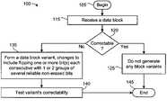
- FIG. 1shows a flowchart of a method of the present invention.
- FIG. 2shows an apparatus of the present invention, including a transmission or storage medium within which a data block will be subject to degradation.
- FIG. 3shows a flowchart of another method the present invention.
- FIG. 4shows a raw quality series that includes a data block and related reliability information.
- FIG. 5shows an ECC block for use in the present invention.
- FIG. 6shows another ECC block for use in the present invention
- FIG. 7shows another control circuit of the present invention.
- FIG. 8shows a series of versions derived from a common data block, useful for reconstructing the data block.
- a “sequence” of bits or symbolsis a consecutively-placed group of values in a linear stream, not a group that is interspersed with other values.
- a “reliable” or “potentially good” bitis one that has a reliability indicator higher than a predetermined threshold and/or an error likelihood indicator lower than a predetermined threshold, for example.
- An “unreliable” or “potentially bad” bitis one that has a reliability indicator lower than a predetermined threshold and/or an error likelihood indicator higher than a predetermined threshold.
- the thresholdis preferably based on empirically derived values of many bits expressed in terms of the selected reliability or likelihood indicator.
- FIG. 1there is shown a flowchart of a method 100 of the present invention, comprising steps 105 through 145 .
- a data blockis received 115 . If it is correctable 120 , such as by an ordinary Error Correction Code, no variants are generated 125 , and the method 100 is deemed successful 145 . If the data block is not correctable 120 , a data block variant is formed 135 . At least one potentially bad bit is identified (such as with soft ECC/quality information) that is isolated, apparently not among other unreliable bits. The variant is then tested 140 for correctability.
- FIG. 2shows an apparatus 200 of the present invention configured to perform any or all of the methods described in this document. It includes a transmission or storage medium 290 that is subject to some form of data degradation, an integrated circuit 250 , an ECC control block 230 , and signal lines.
- Detector 220is configured to received data 214 from channel 210 which has interactions 288 with medium 290 .
- Detector 220optionally contains a buffer 222 containing log likelihood ratios, distances from nearest defined symbols, empirical pattern recognition, and/or other reliability-indicative or soft ECC data each associated with selected portions of a block of the received data 214 .
- the reliability-indicative datamay be partly based on analog information included in the received data 214 . In this case the detector 220 creates the reliability-indicative data partly based on digitized measurements of the analog information.
- a portion 225 of the reliability-indicative datais optionally sent to ECC 230 along with the data block 224 with which the portion 225 is associated. This portion 225 is used to generate a several data objects 227 , 228 , 229 within ECC 230 .
- the data objectsinclude a potentially bad bit series 227 , a potentially bad symbol series 228 , and a flip-bit series 229 .
- ECC 230uses these objects 227 , 228 , 229 for systematic modification of the data block 224 and optionally returns an indication 226 of whether the modified data block is correctable.
- the corrected data blockis provided as a system output 235 .
- FIG. 3shows a flowchart of another method 300 of the present invention, comprising steps 305 through 395 .
- method 300is optionally performed by apparatus 200 of FIG. 2 upon the specific data given in one or more of the FIGS. 4-9 .
- An estimate of an original data blockis received 310 into ECC block 230 , including identifiers of less-reliable bits.
- ECC block 230chooses reliability and isolation criteria 315 and a set of multi-bit symbols to be erased 230 . The chosen symbols are erased 325 , and then some of the non-erased bits are selected 330 using the criteria of step 315 . Preferably any selected bits in the erased symbols are de-selected 340 to conserve resources.
- a new variantis generated 345 and tested 350 , preferably one that differs by several bits from the as-received block(s) and all variants. If the variant is correctable the method 300 was successful. Otherwise, if more variants with that erasure set are warranted and resources permit (as determined by an iteration count threshold comparison at step 355 ), another variant is generated 345 and tested 350 . Otherwise, if other erasure sets are warranted and resources permit (as determined by an iteration count threshold comparison at step 360 ), a new erasure set is generated 362 and applied 325 .
- the attempt to decode the received blockis deemed a failure 365 . If possible, then, another estimate is obtained 385 , such as by receiving a second estimate of the data block from medium 290 . The new estimate can even be a combination of the first and second readings, with differing bits between the two deemed less reliable than consistent bits. If no new estimate can be transmitted 375 , the data reconstruction method 300 is deemed unsuccessful. See FIG. 8 for a specific example using 11 isolated potentially bad bits available for selection, 2 erasure sets and several variants generated for each erasure set.
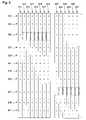
- FIG. 4shows a raw quality series 400 residing in a buffer 422 which is optionally used as buffer 222 of FIG. 2 (simultaneously or sequentially).
- each of the rows 3867 - 3902corresponds with a corresponding bit of a data block to be decoded.
- column 462contains a preliminary estimate of the received data block 224 and column 461 contains a one-bit reliability indicator for each bit of the estimate.
- a “1”signifies a reliable bit and the “0” in row 3884 signifies that bit 410 has been identified as potentially bad.
- potentially bad bit 410has a value of “0” in the preliminary estimate, but that the correctly decoded value may actually be “1.” Although it may be possible to ascertain the correct value of potentially bad bit 410 by a conventional process of error correction, it will be appreciated that performing such a process with a wrong guess can cause the error correction process to fail. A better approach in some circumstances is to try testing block correctability with an untried value of the identified potentially bad bit(s).
- potentially bad bit 410is a desirable candidate for “flipping” by virtue of the fact that it is surrounded by reliable bits, and is therefore isolated from other bits identified as potentially bad.
- the potentially bad bit 410can be selected so that at least P immediately preceding bits are all reliable, where 1 ⁇ P ⁇ 15.
- Potentially bad bit 410can likewise be selected so that at least Q immediately succeeding bits are all reliable, where 1 ⁇ Q ⁇ 15.
- Each potentially bad bit 410can also be selected so that the symbol containing the potentially bad bit contain only that one potentially bad bit. For a still narrower selection of potentially bad bits suitable for flipping, it can be further required that at least 2 to 5 symbols immediately before and/or after the symbol containing the potentially bad bit 410 all consist of reliable bits only.
- raw quality series 400contains additional, mutually independent indicators (e.g. elements in columns 463 , 464 , 465 ) relating to bit or symbol attributes, each pertinent to the bit or symbol associated with that row in the series. These indicators may show whether the “unreliability” determination is based on analog sample data, empirical similarity to previously-identified corrupt symbols, consistency with a previous estimate of the same original data block, indicia of isolation from other potentially bad bits, etc.
- column 461contains the preliminary estimate of the received data block.
- Each symbol of the block to be decodedcontains ten bits. The last digit of the reference numeral gives the bit number of that row's bit, and the other digit(s) give the symbol number.
- Symbol 388for example, contains an estimated value of “1111101111.”
- the first-sent, least-significant bitis given in row 3880 , which also contains 1's in columns 462 , 463 , 464 , 465 .
- FIG. 5shows an ECC block 530 for use in the present invention, optionally used as ECC block 230 in coordination with series 400 in buffer 222 .
- Block 530is optionally configured to perform the method of FIG. 1 or 3 , for example.
- Block 530includes a potentially bad bit series 527 and a potentially bad symbol series 528 .
- Each row of potentially bad bit series 527includes a symbol identifier (in column 561 ), a bit identifier (in column 562 ) and a doubt level (in column 563 , expressed in decimal form).
- Bits 0 , 3 and 6 of symbol 388correspond respectively with rows 3880 , 3883 and 3886 of FIG. 4 , each bit having a doubt level of 15 as shown.
- series 527is simply a summary derived from the contents of the complete raw quality series 400 , only a part of which can be shown in FIG. 4 .
- Potentially bad symbol series 528is also a summary derived from the contents of series 400 .
- the seriesis defined as all of the symbols having a composite reliability below a predetermined threshold.
- the composite reliability of a given symbolis evaluated at least partly based on the doubt levels of several of the reliable bits in the given symbol.
- Several methodsare taught below for computing such reliabilities.
- Some such methodsare described, for example, in U.S. Pat. No. 6,480,552 (“Soft Output Metrics Generator for Symbol Detectors”) issued 12 Nov. 2002 to Tonello; and in U.S. Pat. No. 6,434,719 (“Error Correction Using Reliability Values for Data Matrix”) issued 13 Aug. 2002 to Livingston.
- Potentially bad bit series 527identifies fifteen bits each having a high (saturated) doubt and six bits each having a moderate (e.g. non-saturated but at least 8) doubt, in the present data block.
- series 527implicitly classifies the other bits in the block in a third category, each bit in the third category having a low doubt (at or below 8).
- Despite the low doubt levelsit will be recognized that enough errors may nevertheless occur in these numerous bits that the data block will not initially be correctable. It is sometimes hard to determine how best to modify the block so as to increase the likelihood that the modified block will be correctable. It is generally better to try flipping bits in series 527 , though, than to try flipping other bits in the block.
- Another approachis to erase all of the potentially bad symbols and to expand the potentially bad symbol series 528 to include all symbols that contain any bit in the potentially bad bit series. In the present case this will require the inclusion of 13 additional symbols: 18 , 133 , 164 , 200 , 204 , 236 , 358 , 387 , 389 , 396 , 397 , 398 , and 402 . Erasing such a large number of additional symbols is a significant resource allocation and may be unfeasible.
- FIG. 6shows another ECC block 630 for use in the present invention, optionally used as ECC block 230 in coordination with series 400 in buffer 222 .
- Block 630is optionally a processor configured to perform the method of FIGS. 1 or 3 , for example.
- Block 630contains a potentially bad symbol series 628 and a flip-bit series 629 , both derived from raw quality series 400 of FIG. 4 . The process used or generating the potentially bad symbol series 628 is described first. An intermediate calculation is generated for a potentially bad bit of a selected symbol, the intermediate calculation being the sum of the 4-digit doubt levels of the 3 preceding bits and the 3 succeeding bits.
- this intermediate calculationis 8+15+6+15+3+1, which is 48 decimal.
- the selected symbol's reliability scorein this example, is the negative of the largest of the ten intermediate values for the selected symbol. None of the other intermediate calculations for symbol 388 of FIG. 4 are larger than 48, so symbol 388 's reliability score is negative 48. In the present data block, this is the second lowest reliability score.
- the ten least reliable symbols of the blockare given in series 628 , in descending order of reliability.
- flip-bit series 629is accordingly derived as all bits in the data block with a doubt level of at least 8 that are not identified in the potentially bad symbol series 628 .
- the same series 629can alternatively be derived as the 15 most-doubted bits in the data block that are not identified in the potentially bad symbol series 628 .
- series 629is derived first by collecting all of the rows with a doubt level of 15 as space permits in a fixed-length buffer. Then rows from each next-highest doubt level are added until the fixed-length buffer is filled, 15 rows in the present case. In a typical case, though, a simple threshold may be selected so as to avoid the need for any sorting.
- the threshold of doubtis set much higher, which is to say that the threshold of reliability is set much lower.
- Thiscan be accomplished, for example, by setting X so that C ⁇ 2 ⁇ X ⁇ C+20.
- the emphasis in this caseis to test a diverse selection of the combinations, preferably by an approach described below with reference to FIG. 8 .
- FIG. 7shows another control circuit 700 of the present invention containing a series 727 of identifiers of doubted bits, a selected subset 729 of series 727 , and a series 728 of symbol identifiers.
- Circuit 700is optionally configured to perform the method of FIG. 1 or 3 , for example.
- Each bit in series 727is identified by a symbol number 731 and a bit number 732 .
- Each bit in subset series 727is similarly identified by a symbol number 761 and a bit number 762 .
- These series 727 , 728 , 729can be stored in the detector 220 and/or ECC 230 of FIG. 2 , or they can be determined and used sequentially, without being stored.
- Symbol identifier series 728can be determined in a manner similar to that of potentially bad symbol series 628 of FIG. 6 , but using a simpler calculation to obtain each bit's calculation. Relative to each selected bit, doubt levels of all bits of the selected symbol, the previous symbol and the next symbol are simply added. For any bit of symbol 388 (from near symbol 388 of FIG. 4 ) this doubt-indicative calculation is (3+1+3+0+1+1+15+1+1+8)+(15+6+6+15+3+1+15+0+7+6)+(15+0+1+2+7+2+0+1+3+0), which is 139 decimal. Note that this is less costly than prior embodiments in that only one such calculation need be performed for each symbol. The 25 least reliable symbols of the block are given in series 728 according to this system of evaluation.
- FIG. 7demonstrates that a series of potentially bad symbols that is better aligned with a series of doubted bits allows a short flip-bit series 729 to account for an even larger set of potentially bad bits (e.g. the first 25 listed in series 727 ). It is still generally preferable to flip isolated doubted bits, however, leaving the symbol otherwise intact to which the isolated doubted bit belongs.
- FIG. 8shows a preliminary data block 871 that estimates the value of an original data block, and a series of several variants 872 , 873 , 874 , 875 , 876 , 877 , 878 , 879 , 882 , 883 , 884 , 885 , 886 , 887 of the preliminary data block 871 .
- Values of several potentially bad bits 821 , 823 , 825 , 827 , 829 , 831 , 833 , 835 , 837 , 839 , 841 of each of the data block versions 871 - 887are shown explicitly, with the content of sequences of many reliable bits indicated by ellipses, interleaved with the potentially bad bits.
- each one of the block versions 871 - 887most of the potentially bad bits 823 - 841 are each situated in a respective block portion among several reliable bits. Each of these is consecutive with 2 sequences of several potentially good bits.
- the first variant 872has all potentially bad bits un-flipped, but includes an erased symbol containing potentially bad bit 825 .
- Variant 873has four potentially bad bits 821 , 823 , 827 , 831 flipped.
- Variant 874has a different set of four potentially bad bits 823 , 831 , 835 , 837 flipped.
- the next four variants 875 , 876 , 877 , 878have sets of 5,6,7, and 3 bits flipped, respectively.
- each new varianthas a set of bits selected by a pseudo-random sequence generator from among an isolated potentially bad bit series.
- most of the inter-variant transitionswill cause at least 4-5 of these bits to transition, but not more than 70% of these bit values should usually be flipped within a given variant.
- at least one of the flip-bitsshould be kept in its un-flipped state more than 70% of the time.
- bit 833is “moderately unreliable” and is thus kept un-flipped in at least 80% of the variants formed.
- each of the variants 872 - 878is found to be non-correctable, in sequence.
- Variant 882is then formed as the preliminary data block 871 with a new symbol erasure set, distinct from that of variant 872 . This manifests itself as an erased symbol that includes potentially bad bit 837 , so that bit 837 need not be a “selected bit” on the flip-bit list.
- variants 882 - 887are formed and each found to be non-correctable.
- 2 erasure setsare “enough” at step 360 , so that a decode failure occurs 365 .
- the best chance for data recoveryis a re-transmit used to generate a new estimate 385 , without which the data recovery method fails 395 .
- each flip-bit series for the embodiment of FIG. 8is selected to include several isolated potentially bad bits each of which is the only unreliable bit (i.e. below a predetermined reliability threshold) in its respective symbol.
- a symbol erasure seriesis generated later so as to exclude any symbol that includes any bit in the flip-bit series. Choosing a symbol erasure series after the flip-bit series simplifies computation for the flip-bit selection step while allowing the most suitable selection of bits to be selected for flipping.
- a first embodiment of the present inventionis a method (such as 100 , 300 ) comprising a step of performing a variant correctability test (such as 140 , 350 ) upon a data block variant formed from a received data block by a variation process that includes flipping a selected, potentially bad bit (such as 831 ) that is consecutive with several potentially good bits of the received block.
- the variant correctability testis optionally repeated several times (such as by step 355 ) before receiving another data block, each repetition using a different block variant (such as by step 345 ).
- another blockis subsequently received (such as by step 385 ), each of the received data blocks being an estimate of one original data block.
- the performing stepis done so that the data block variant includes at least 1-2 erased symbol(s) and so that the erased symbol(s) do not contain any flipped bits (such as by step 340 ). All of the symbols have N bits, and each flipped bit is preferably selected as a potentially bad bit isolated enough so that the other N-1 bits are all reliable, in the symbol that contains the flipped bit.
- an original data blockis first sent into a storage or transmission medium (such as 290 ) where degradation can occur.
- the received data blockis later derived from this original data block.
- a control block(such as 230 ) performs the flip-bit selection based at least partly on an arithmetic combination of scalar evaluations of each of the several potentially good bits (such as by step 330 implementing any of FIGS. 4-8 ).
- a fourth alternative embodiment of the present inventionis a method including at least four steps.
- the first stepis determining whether to perform a variant correctability test upon a data block variant primarily based on whether a received data block is correctable (such as by step 120 ).
- the second stepis selecting at least partly based on at least first, second, and third non-overlapping bit reliability categories so that the first category includes many selected bits, so that the second category includes several potentially good non-selected bits, so that the third category includes several other non-selected bits of the received block, and so that each of the selected bits meets at least one predetermined criterion of a minimum mutual isolation (such as by step 330 implementing any of FIGS. 4-8 ).
- the third stepis forming the data block variant by flipping several of the many selected received bits, the flipped bits each consecutive with 2 sequences of several potentially good bits of the received block and by erasing several symbols each consisting of some of the non-selected bits (such as by step 345 implementing FIG. 8 ).
- the fourth stepis determining, based on the variant correctability test, whether to perform another variant correctability test upon another data block variant formed by flipping another of the selected bits (such as by step 355 ).
- a fifth alternative embodimentis a method comprising a step of determining based on a received data block whether to perform a variant correctability test upon a data block variant formed by flipping a first potentially bad bit that is consecutive with several potentially good bits of the received block (such as by method 100 or 300 ). This first variant correctability test is then used to determine whether to perform another variant correctability test (such as by step 355 ).
- a sixth alternative embodimentis an apparatus configured to perform one of the methods of the present invention.
- the apparatusincludes a medium within which a data block is vulnerable to degradation.
Landscapes
- Physics & Mathematics (AREA)
- Probability & Statistics with Applications (AREA)
- Engineering & Computer Science (AREA)
- Theoretical Computer Science (AREA)
- Mathematical Physics (AREA)
- Detection And Correction Of Errors (AREA)
- Error Detection And Correction (AREA)
Abstract
Description
Claims (29)
Priority Applications (1)
| Application Number | Priority Date | Filing Date | Title |
|---|---|---|---|
| US10/869,447US7447970B2 (en) | 2004-06-16 | 2004-06-16 | Soft-decision decoding using selective bit flipping |
Applications Claiming Priority (1)
| Application Number | Priority Date | Filing Date | Title |
|---|---|---|---|
| US10/869,447US7447970B2 (en) | 2004-06-16 | 2004-06-16 | Soft-decision decoding using selective bit flipping |
Publications (2)
| Publication Number | Publication Date |
|---|---|
| US20050283702A1 US20050283702A1 (en) | 2005-12-22 |
| US7447970B2true US7447970B2 (en) | 2008-11-04 |
Family
ID=35481993
Family Applications (1)
| Application Number | Title | Priority Date | Filing Date |
|---|---|---|---|
| US10/869,447Active2025-12-01US7447970B2 (en) | 2004-06-16 | 2004-06-16 | Soft-decision decoding using selective bit flipping |
Country Status (1)
| Country | Link |
|---|---|
| US (1) | US7447970B2 (en) |
Cited By (52)
| Publication number | Priority date | Publication date | Assignee | Title |
|---|---|---|---|---|
| US20080168021A1 (en)* | 2007-01-05 | 2008-07-10 | Fujitsu Limited | Reliability evaluation program and reliability evaluation device |
| US20090144600A1 (en)* | 2007-11-30 | 2009-06-04 | Anobit Technologies Ltd | Efficient re-read operations from memory devices |
| US8145984B2 (en) | 2006-10-30 | 2012-03-27 | Anobit Technologies Ltd. | Reading memory cells using multiple thresholds |
| US8151166B2 (en) | 2007-01-24 | 2012-04-03 | Anobit Technologies Ltd. | Reduction of back pattern dependency effects in memory devices |
| US8151163B2 (en) | 2006-12-03 | 2012-04-03 | Anobit Technologies Ltd. | Automatic defect management in memory devices |
| US8156403B2 (en) | 2006-05-12 | 2012-04-10 | Anobit Technologies Ltd. | Combined distortion estimation and error correction coding for memory devices |
| US8156398B2 (en) | 2008-02-05 | 2012-04-10 | Anobit Technologies Ltd. | Parameter estimation based on error correction code parity check equations |
| US8169825B1 (en) | 2008-09-02 | 2012-05-01 | Anobit Technologies Ltd. | Reliable data storage in analog memory cells subjected to long retention periods |
| US8174905B2 (en) | 2007-09-19 | 2012-05-08 | Anobit Technologies Ltd. | Programming orders for reducing distortion in arrays of multi-level analog memory cells |
| US8174857B1 (en) | 2008-12-31 | 2012-05-08 | Anobit Technologies Ltd. | Efficient readout schemes for analog memory cell devices using multiple read threshold sets |
| US8208304B2 (en) | 2008-11-16 | 2012-06-26 | Anobit Technologies Ltd. | Storage at M bits/cell density in N bits/cell analog memory cell devices, M>N |
| US8209588B2 (en) | 2007-12-12 | 2012-06-26 | Anobit Technologies Ltd. | Efficient interference cancellation in analog memory cell arrays |
| US8230300B2 (en) | 2008-03-07 | 2012-07-24 | Apple Inc. | Efficient readout from analog memory cells using data compression |
| US8228701B2 (en) | 2009-03-01 | 2012-07-24 | Apple Inc. | Selective activation of programming schemes in analog memory cell arrays |
| US8234545B2 (en) | 2007-05-12 | 2012-07-31 | Apple Inc. | Data storage with incremental redundancy |
| US8239735B2 (en) | 2006-05-12 | 2012-08-07 | Apple Inc. | Memory Device with adaptive capacity |
| US8238157B1 (en) | 2009-04-12 | 2012-08-07 | Apple Inc. | Selective re-programming of analog memory cells |
| US8239734B1 (en) | 2008-10-15 | 2012-08-07 | Apple Inc. | Efficient data storage in storage device arrays |
| US8248831B2 (en) | 2008-12-31 | 2012-08-21 | Apple Inc. | Rejuvenation of analog memory cells |
| US8259497B2 (en) | 2007-08-06 | 2012-09-04 | Apple Inc. | Programming schemes for multi-level analog memory cells |
| US8261159B1 (en) | 2008-10-30 | 2012-09-04 | Apple, Inc. | Data scrambling schemes for memory devices |
| US8259506B1 (en) | 2009-03-25 | 2012-09-04 | Apple Inc. | Database of memory read thresholds |
| US8270246B2 (en) | 2007-11-13 | 2012-09-18 | Apple Inc. | Optimized selection of memory chips in multi-chips memory devices |
| US8369141B2 (en) | 2007-03-12 | 2013-02-05 | Apple Inc. | Adaptive estimation of memory cell read thresholds |
| US8400858B2 (en) | 2008-03-18 | 2013-03-19 | Apple Inc. | Memory device with reduced sense time readout |
| US8429493B2 (en) | 2007-05-12 | 2013-04-23 | Apple Inc. | Memory device with internal signap processing unit |
| US8479080B1 (en) | 2009-07-12 | 2013-07-02 | Apple Inc. | Adaptive over-provisioning in memory systems |
| US8482978B1 (en) | 2008-09-14 | 2013-07-09 | Apple Inc. | Estimation of memory cell read thresholds by sampling inside programming level distribution intervals |
| US8495465B1 (en) | 2009-10-15 | 2013-07-23 | Apple Inc. | Error correction coding over multiple memory pages |
| US8493781B1 (en) | 2010-08-12 | 2013-07-23 | Apple Inc. | Interference mitigation using individual word line erasure operations |
| US8493783B2 (en) | 2008-03-18 | 2013-07-23 | Apple Inc. | Memory device readout using multiple sense times |
| US8498151B1 (en) | 2008-08-05 | 2013-07-30 | Apple Inc. | Data storage in analog memory cells using modified pass voltages |
| US8527819B2 (en) | 2007-10-19 | 2013-09-03 | Apple Inc. | Data storage in analog memory cell arrays having erase failures |
| US8572423B1 (en) | 2010-06-22 | 2013-10-29 | Apple Inc. | Reducing peak current in memory systems |
| US8572311B1 (en) | 2010-01-11 | 2013-10-29 | Apple Inc. | Redundant data storage in multi-die memory systems |
| US8570804B2 (en) | 2006-05-12 | 2013-10-29 | Apple Inc. | Distortion estimation and cancellation in memory devices |
| US8595591B1 (en) | 2010-07-11 | 2013-11-26 | Apple Inc. | Interference-aware assignment of programming levels in analog memory cells |
| US8645794B1 (en) | 2010-07-31 | 2014-02-04 | Apple Inc. | Data storage in analog memory cells using a non-integer number of bits per cell |
| US8677054B1 (en) | 2009-12-16 | 2014-03-18 | Apple Inc. | Memory management schemes for non-volatile memory devices |
| US8694854B1 (en) | 2010-08-17 | 2014-04-08 | Apple Inc. | Read threshold setting based on soft readout statistics |
| US8694814B1 (en) | 2010-01-10 | 2014-04-08 | Apple Inc. | Reuse of host hibernation storage space by memory controller |
| US8694853B1 (en) | 2010-05-04 | 2014-04-08 | Apple Inc. | Read commands for reading interfering memory cells |
| US8832354B2 (en) | 2009-03-25 | 2014-09-09 | Apple Inc. | Use of host system resources by memory controller |
| US8856475B1 (en) | 2010-08-01 | 2014-10-07 | Apple Inc. | Efficient selection of memory blocks for compaction |
| US8924661B1 (en) | 2009-01-18 | 2014-12-30 | Apple Inc. | Memory system including a controller and processors associated with memory devices |
| US8949684B1 (en) | 2008-09-02 | 2015-02-03 | Apple Inc. | Segmented data storage |
| US9021181B1 (en) | 2010-09-27 | 2015-04-28 | Apple Inc. | Memory management for unifying memory cell conditions by using maximum time intervals |
| US9104580B1 (en) | 2010-07-27 | 2015-08-11 | Apple Inc. | Cache memory for hybrid disk drives |
| TWI549135B (en)* | 2013-11-08 | 2016-09-11 | 愛思開海力士有限公司 | Threshold estimation using bit flip counts and minimums |
| US20170139769A1 (en)* | 2015-11-13 | 2017-05-18 | Samsung Electronics Co., Ltd. | Method and apparatus for encoding and decoding data in memory system |
| US11556416B2 (en) | 2021-05-05 | 2023-01-17 | Apple Inc. | Controlling memory readout reliability and throughput by adjusting distance between read thresholds |
| US11847342B2 (en) | 2021-07-28 | 2023-12-19 | Apple Inc. | Efficient transfer of hard data and confidence levels in reading a nonvolatile memory |
Families Citing this family (7)
| Publication number | Priority date | Publication date | Assignee | Title |
|---|---|---|---|---|
| US7782984B2 (en)* | 2002-08-30 | 2010-08-24 | Alcatel-Lucent Usa Inc. | Method of sphere decoding with low complexity and good statistical output |
| US7328395B1 (en) | 2004-04-13 | 2008-02-05 | Marvell International Ltd. | Iterative Reed-Solomon error-correction decoding |
| CN101923896A (en)* | 2009-06-12 | 2010-12-22 | 威刚科技(苏州)有限公司 | Electronic storage device and error correcting method thereof |
| WO2013159364A1 (en)* | 2012-04-28 | 2013-10-31 | 华为技术有限公司 | Method for repairing and decoding air interface voice frame, and signal source side information acquisition method and device |
| US10313053B2 (en)* | 2013-08-23 | 2019-06-04 | Myriota Pty Ltd | Enhanced automatic identification system |
| RU2725699C1 (en)* | 2019-08-27 | 2020-07-03 | Акционерное общество "Калужский научно-исследовательский институт телемеханических устройств" | Method for soft decoding of noise-immune code |
| RU2738724C1 (en)* | 2020-06-02 | 2020-12-16 | Акционерное общество "Калужский научно-исследовательский институт телемеханических устройств" | Method for soft decoding of a noise-immune code |
Citations (16)
| Publication number | Priority date | Publication date | Assignee | Title |
|---|---|---|---|---|
| US5373513A (en)* | 1991-08-16 | 1994-12-13 | Eastman Kodak Company | Shift correction code system for correcting additive errors and synchronization slips |
| US5933462A (en) | 1996-11-06 | 1999-08-03 | Qualcomm Incorporated | Soft decision output decoder for decoding convolutionally encoded codewords |
| US5936972A (en) | 1997-06-18 | 1999-08-10 | Motorola, Inc. | Syndrome-based channel quality or message structure determiner |
| US20010054170A1 (en) | 2000-01-07 | 2001-12-20 | Amir Chass | Apparatus and method for performing parallel SISO decoding |
| US6389574B1 (en) | 1998-03-25 | 2002-05-14 | Matra Nortel Communications | Method for detecting a discrete symbol sequence from an observation signal, and viterbi processor implementing such method |
| US6434719B1 (en) | 1999-05-07 | 2002-08-13 | Cirrus Logic Inc. | Error correction using reliability values for data matrix |
| US6480552B1 (en) | 1999-03-24 | 2002-11-12 | Lucent Technologies Inc. | Soft output metrics generation for symbol detectors |
| US6484285B1 (en) | 2000-02-07 | 2002-11-19 | Ericsson, Inc. | Tailbiting decoder and method |
| US6587987B1 (en) | 2000-07-07 | 2003-07-01 | Lucent Technologies Inc. | Method and apparatus for extracting reliability information from partial response channels |
| US6597743B1 (en) | 1999-12-07 | 2003-07-22 | Ericsson Inc. | Reduced search symbol estimation algorithm |
| US6628837B1 (en) | 2000-05-19 | 2003-09-30 | Xerox Corporation | Assist channel coding with convolution coding |
| US6665357B1 (en) | 1999-01-22 | 2003-12-16 | Sharp Laboratories Of America, Inc. | Soft-output turbo code decoder and optimized decoding method |
| US6671338B1 (en) | 1998-11-12 | 2003-12-30 | Hughes Electronics Corporation | Combined interference cancellation with FEC decoding for high spectral efficiency satellite communications |
| US6691263B2 (en) | 2001-05-03 | 2004-02-10 | Agere Systems Inc. | Interative decoding based on dominant error events |
| US6697441B1 (en) | 2000-06-06 | 2004-02-24 | Ericsson Inc. | Baseband processors and methods and systems for decoding a received signal having a transmitter or channel induced coupling between bits |
| US6999531B2 (en) | 2000-03-01 | 2006-02-14 | 1021 Technologies Kk | Soft-decision decoding of convolutionally encoded codeword |
- 2004
- 2004-06-16USUS10/869,447patent/US7447970B2/enactiveActive
Patent Citations (16)
| Publication number | Priority date | Publication date | Assignee | Title |
|---|---|---|---|---|
| US5373513A (en)* | 1991-08-16 | 1994-12-13 | Eastman Kodak Company | Shift correction code system for correcting additive errors and synchronization slips |
| US5933462A (en) | 1996-11-06 | 1999-08-03 | Qualcomm Incorporated | Soft decision output decoder for decoding convolutionally encoded codewords |
| US5936972A (en) | 1997-06-18 | 1999-08-10 | Motorola, Inc. | Syndrome-based channel quality or message structure determiner |
| US6389574B1 (en) | 1998-03-25 | 2002-05-14 | Matra Nortel Communications | Method for detecting a discrete symbol sequence from an observation signal, and viterbi processor implementing such method |
| US6671338B1 (en) | 1998-11-12 | 2003-12-30 | Hughes Electronics Corporation | Combined interference cancellation with FEC decoding for high spectral efficiency satellite communications |
| US6665357B1 (en) | 1999-01-22 | 2003-12-16 | Sharp Laboratories Of America, Inc. | Soft-output turbo code decoder and optimized decoding method |
| US6480552B1 (en) | 1999-03-24 | 2002-11-12 | Lucent Technologies Inc. | Soft output metrics generation for symbol detectors |
| US6434719B1 (en) | 1999-05-07 | 2002-08-13 | Cirrus Logic Inc. | Error correction using reliability values for data matrix |
| US6597743B1 (en) | 1999-12-07 | 2003-07-22 | Ericsson Inc. | Reduced search symbol estimation algorithm |
| US20010054170A1 (en) | 2000-01-07 | 2001-12-20 | Amir Chass | Apparatus and method for performing parallel SISO decoding |
| US6484285B1 (en) | 2000-02-07 | 2002-11-19 | Ericsson, Inc. | Tailbiting decoder and method |
| US6999531B2 (en) | 2000-03-01 | 2006-02-14 | 1021 Technologies Kk | Soft-decision decoding of convolutionally encoded codeword |
| US6628837B1 (en) | 2000-05-19 | 2003-09-30 | Xerox Corporation | Assist channel coding with convolution coding |
| US6697441B1 (en) | 2000-06-06 | 2004-02-24 | Ericsson Inc. | Baseband processors and methods and systems for decoding a received signal having a transmitter or channel induced coupling between bits |
| US6587987B1 (en) | 2000-07-07 | 2003-07-01 | Lucent Technologies Inc. | Method and apparatus for extracting reliability information from partial response channels |
| US6691263B2 (en) | 2001-05-03 | 2004-02-10 | Agere Systems Inc. | Interative decoding based on dominant error events |
Non-Patent Citations (1)
| Title |
|---|
| Chan et al., A simple taboo-based soft decision decoding algorithm for expander codes, 1998, IEEE, p. 183-185.* |
Cited By (67)
| Publication number | Priority date | Publication date | Assignee | Title |
|---|---|---|---|---|
| US8599611B2 (en) | 2006-05-12 | 2013-12-03 | Apple Inc. | Distortion estimation and cancellation in memory devices |
| US8156403B2 (en) | 2006-05-12 | 2012-04-10 | Anobit Technologies Ltd. | Combined distortion estimation and error correction coding for memory devices |
| US8239735B2 (en) | 2006-05-12 | 2012-08-07 | Apple Inc. | Memory Device with adaptive capacity |
| US8570804B2 (en) | 2006-05-12 | 2013-10-29 | Apple Inc. | Distortion estimation and cancellation in memory devices |
| US8145984B2 (en) | 2006-10-30 | 2012-03-27 | Anobit Technologies Ltd. | Reading memory cells using multiple thresholds |
| USRE46346E1 (en) | 2006-10-30 | 2017-03-21 | Apple Inc. | Reading memory cells using multiple thresholds |
| US8151163B2 (en) | 2006-12-03 | 2012-04-03 | Anobit Technologies Ltd. | Automatic defect management in memory devices |
| US20080168021A1 (en)* | 2007-01-05 | 2008-07-10 | Fujitsu Limited | Reliability evaluation program and reliability evaluation device |
| US7856412B2 (en)* | 2007-01-05 | 2010-12-21 | Fujitsu Limited | Reliability evaluation program and reliability evaluation device |
| US8151166B2 (en) | 2007-01-24 | 2012-04-03 | Anobit Technologies Ltd. | Reduction of back pattern dependency effects in memory devices |
| US8369141B2 (en) | 2007-03-12 | 2013-02-05 | Apple Inc. | Adaptive estimation of memory cell read thresholds |
| US8429493B2 (en) | 2007-05-12 | 2013-04-23 | Apple Inc. | Memory device with internal signap processing unit |
| US8234545B2 (en) | 2007-05-12 | 2012-07-31 | Apple Inc. | Data storage with incremental redundancy |
| US8259497B2 (en) | 2007-08-06 | 2012-09-04 | Apple Inc. | Programming schemes for multi-level analog memory cells |
| US8174905B2 (en) | 2007-09-19 | 2012-05-08 | Anobit Technologies Ltd. | Programming orders for reducing distortion in arrays of multi-level analog memory cells |
| US8527819B2 (en) | 2007-10-19 | 2013-09-03 | Apple Inc. | Data storage in analog memory cell arrays having erase failures |
| US8270246B2 (en) | 2007-11-13 | 2012-09-18 | Apple Inc. | Optimized selection of memory chips in multi-chips memory devices |
| US8990659B2 (en)* | 2007-11-30 | 2015-03-24 | Apple Inc. | Efficient re-read operations in analog memory cell arrays |
| US20090144600A1 (en)* | 2007-11-30 | 2009-06-04 | Anobit Technologies Ltd | Efficient re-read operations from memory devices |
| US8769381B2 (en)* | 2007-11-30 | 2014-07-01 | Apple Inc. | Efficient re-read operations in analog memory cell arrays |
| US8225181B2 (en)* | 2007-11-30 | 2012-07-17 | Apple Inc. | Efficient re-read operations from memory devices |
| US20140325308A1 (en)* | 2007-11-30 | 2014-10-30 | Apple Inc. | Efficient Re-read Operations in Analog Memory Cell Arrays |
| US8782497B2 (en)* | 2007-11-30 | 2014-07-15 | Apple Inc. | Efficient re-read operations in analog memory cell arrays |
| US8209588B2 (en) | 2007-12-12 | 2012-06-26 | Anobit Technologies Ltd. | Efficient interference cancellation in analog memory cell arrays |
| US8156398B2 (en) | 2008-02-05 | 2012-04-10 | Anobit Technologies Ltd. | Parameter estimation based on error correction code parity check equations |
| US8230300B2 (en) | 2008-03-07 | 2012-07-24 | Apple Inc. | Efficient readout from analog memory cells using data compression |
| US8400858B2 (en) | 2008-03-18 | 2013-03-19 | Apple Inc. | Memory device with reduced sense time readout |
| US8493783B2 (en) | 2008-03-18 | 2013-07-23 | Apple Inc. | Memory device readout using multiple sense times |
| US8498151B1 (en) | 2008-08-05 | 2013-07-30 | Apple Inc. | Data storage in analog memory cells using modified pass voltages |
| US8949684B1 (en) | 2008-09-02 | 2015-02-03 | Apple Inc. | Segmented data storage |
| US8169825B1 (en) | 2008-09-02 | 2012-05-01 | Anobit Technologies Ltd. | Reliable data storage in analog memory cells subjected to long retention periods |
| US8482978B1 (en) | 2008-09-14 | 2013-07-09 | Apple Inc. | Estimation of memory cell read thresholds by sampling inside programming level distribution intervals |
| US8239734B1 (en) | 2008-10-15 | 2012-08-07 | Apple Inc. | Efficient data storage in storage device arrays |
| US8261159B1 (en) | 2008-10-30 | 2012-09-04 | Apple, Inc. | Data scrambling schemes for memory devices |
| US8713330B1 (en) | 2008-10-30 | 2014-04-29 | Apple Inc. | Data scrambling in memory devices |
| US8208304B2 (en) | 2008-11-16 | 2012-06-26 | Anobit Technologies Ltd. | Storage at M bits/cell density in N bits/cell analog memory cell devices, M>N |
| US8397131B1 (en) | 2008-12-31 | 2013-03-12 | Apple Inc. | Efficient readout schemes for analog memory cell devices |
| US8374014B2 (en) | 2008-12-31 | 2013-02-12 | Apple Inc. | Rejuvenation of analog memory cells |
| US8248831B2 (en) | 2008-12-31 | 2012-08-21 | Apple Inc. | Rejuvenation of analog memory cells |
| US8174857B1 (en) | 2008-12-31 | 2012-05-08 | Anobit Technologies Ltd. | Efficient readout schemes for analog memory cell devices using multiple read threshold sets |
| US8924661B1 (en) | 2009-01-18 | 2014-12-30 | Apple Inc. | Memory system including a controller and processors associated with memory devices |
| US8228701B2 (en) | 2009-03-01 | 2012-07-24 | Apple Inc. | Selective activation of programming schemes in analog memory cell arrays |
| US8259506B1 (en) | 2009-03-25 | 2012-09-04 | Apple Inc. | Database of memory read thresholds |
| US8832354B2 (en) | 2009-03-25 | 2014-09-09 | Apple Inc. | Use of host system resources by memory controller |
| US8238157B1 (en) | 2009-04-12 | 2012-08-07 | Apple Inc. | Selective re-programming of analog memory cells |
| US8479080B1 (en) | 2009-07-12 | 2013-07-02 | Apple Inc. | Adaptive over-provisioning in memory systems |
| US8495465B1 (en) | 2009-10-15 | 2013-07-23 | Apple Inc. | Error correction coding over multiple memory pages |
| US8677054B1 (en) | 2009-12-16 | 2014-03-18 | Apple Inc. | Memory management schemes for non-volatile memory devices |
| US8694814B1 (en) | 2010-01-10 | 2014-04-08 | Apple Inc. | Reuse of host hibernation storage space by memory controller |
| US8572311B1 (en) | 2010-01-11 | 2013-10-29 | Apple Inc. | Redundant data storage in multi-die memory systems |
| US8677203B1 (en) | 2010-01-11 | 2014-03-18 | Apple Inc. | Redundant data storage schemes for multi-die memory systems |
| US8694853B1 (en) | 2010-05-04 | 2014-04-08 | Apple Inc. | Read commands for reading interfering memory cells |
| US8572423B1 (en) | 2010-06-22 | 2013-10-29 | Apple Inc. | Reducing peak current in memory systems |
| US8595591B1 (en) | 2010-07-11 | 2013-11-26 | Apple Inc. | Interference-aware assignment of programming levels in analog memory cells |
| US9104580B1 (en) | 2010-07-27 | 2015-08-11 | Apple Inc. | Cache memory for hybrid disk drives |
| US8645794B1 (en) | 2010-07-31 | 2014-02-04 | Apple Inc. | Data storage in analog memory cells using a non-integer number of bits per cell |
| US8767459B1 (en) | 2010-07-31 | 2014-07-01 | Apple Inc. | Data storage in analog memory cells across word lines using a non-integer number of bits per cell |
| US8856475B1 (en) | 2010-08-01 | 2014-10-07 | Apple Inc. | Efficient selection of memory blocks for compaction |
| US8493781B1 (en) | 2010-08-12 | 2013-07-23 | Apple Inc. | Interference mitigation using individual word line erasure operations |
| US8694854B1 (en) | 2010-08-17 | 2014-04-08 | Apple Inc. | Read threshold setting based on soft readout statistics |
| US9021181B1 (en) | 2010-09-27 | 2015-04-28 | Apple Inc. | Memory management for unifying memory cell conditions by using maximum time intervals |
| TWI549135B (en)* | 2013-11-08 | 2016-09-11 | 愛思開海力士有限公司 | Threshold estimation using bit flip counts and minimums |
| US9812193B2 (en) | 2013-11-08 | 2017-11-07 | SK Hynix Inc. | Threshold estimation using bit flip counts and minimums |
| US20170139769A1 (en)* | 2015-11-13 | 2017-05-18 | Samsung Electronics Co., Ltd. | Method and apparatus for encoding and decoding data in memory system |
| US9792176B2 (en)* | 2015-11-13 | 2017-10-17 | Samsung Electronics Co., Ltd. | Method and apparatus for encoding and decoding data in memory system |
| US11556416B2 (en) | 2021-05-05 | 2023-01-17 | Apple Inc. | Controlling memory readout reliability and throughput by adjusting distance between read thresholds |
| US11847342B2 (en) | 2021-07-28 | 2023-12-19 | Apple Inc. | Efficient transfer of hard data and confidence levels in reading a nonvolatile memory |
Also Published As
| Publication number | Publication date |
|---|---|
| US20050283702A1 (en) | 2005-12-22 |
Similar Documents
| Publication | Publication Date | Title |
|---|---|---|
| US7447970B2 (en) | Soft-decision decoding using selective bit flipping | |
| US5577053A (en) | Method and apparatus for decoder optimization | |
| US8132082B2 (en) | Architecture and control of Reed-Solomon error-correction decoding | |
| AU650399B1 (en) | Improved error correcting decoder and decoding method for receivers in digital cellular communication | |
| US7634706B1 (en) | Majority-detected erasure enhanced error correction | |
| CN101867379B (en) | A Decoding Method of Convolutional Codes Aided by Cyclic Redundancy Check | |
| US8127216B2 (en) | Reduced state soft output processing | |
| US20090132894A1 (en) | Soft Output Bit Threshold Error Correction | |
| US8407569B1 (en) | Error event processing methods and systems | |
| WO1996008895A9 (en) | Method and apparatus for decoder optimization | |
| US20100169746A1 (en) | Low-complexity soft-decision decoding of error-correction codes | |
| US9419651B2 (en) | Non-polynomial processing unit for soft-decision error correction coding | |
| US7325183B2 (en) | Error correction code generation method and apparatus | |
| CN102545914B (en) | BCH (Broadcast Channel) encoding and decoding method and device | |
| US8245106B2 (en) | Method for error correction and error detection of binary data | |
| CN103733521A (en) | Error-correcting decoder | |
| CN101674155B (en) | Digital communication device and decoding method | |
| JP2008118327A (en) | Viterbi decoding method | |
| KR100975060B1 (en) | Error correction method and device for low density parity check | |
| US6956508B2 (en) | Demodulation apparatus and method using code table that decreases complexity | |
| Ding et al. | An efficient joint decoding scheme for outer codes in DNA-based data storage | |
| CN108281160B (en) | Design method of DVD error correction code | |
| US7254771B1 (en) | Error-erasure decoding of interleaved reed-solomon code | |
| Albanese et al. | Two algorithms for soft-decision decoding of reed-solomon codes, with application to multilevel coded modulations | |
| CN120123141B (en) | Coding and decoding method, device and electronic equipment |
Legal Events
| Date | Code | Title | Description |
|---|---|---|---|
| AS | Assignment | Owner name:SEAGATE TECHNOLOGY, LLC, CALIFORNIA Free format text:ASSIGNMENT OF ASSIGNORS INTEREST;ASSIGNORS:WU, YINGQUAN;SILVUS,GREGORY L.;SOUVIGNIER, THOMAS V.;REEL/FRAME:015488/0273;SIGNING DATES FROM 20040609 TO 20040615 | |
| STCF | Information on status: patent grant | Free format text:PATENTED CASE | |
| AS | Assignment | Owner name:WELLS FARGO BANK, NATIONAL ASSOCIATION, AS COLLATERAL AGENT AND SECOND PRIORITY REPRESENTATIVE, CALIFORNIA Free format text:SECURITY AGREEMENT;ASSIGNORS:MAXTOR CORPORATION;SEAGATE TECHNOLOGY LLC;SEAGATE TECHNOLOGY INTERNATIONAL;REEL/FRAME:022757/0017 Effective date:20090507 Owner name:JPMORGAN CHASE BANK, N.A., AS ADMINISTRATIVE AGENT AND FIRST PRIORITY REPRESENTATIVE, NEW YORK Free format text:SECURITY AGREEMENT;ASSIGNORS:MAXTOR CORPORATION;SEAGATE TECHNOLOGY LLC;SEAGATE TECHNOLOGY INTERNATIONAL;REEL/FRAME:022757/0017 Effective date:20090507 Owner name:JPMORGAN CHASE BANK, N.A., AS ADMINISTRATIVE AGENT Free format text:SECURITY AGREEMENT;ASSIGNORS:MAXTOR CORPORATION;SEAGATE TECHNOLOGY LLC;SEAGATE TECHNOLOGY INTERNATIONAL;REEL/FRAME:022757/0017 Effective date:20090507 Owner name:WELLS FARGO BANK, NATIONAL ASSOCIATION, AS COLLATE Free format text:SECURITY AGREEMENT;ASSIGNORS:MAXTOR CORPORATION;SEAGATE TECHNOLOGY LLC;SEAGATE TECHNOLOGY INTERNATIONAL;REEL/FRAME:022757/0017 Effective date:20090507 | |
| AS | Assignment | Owner name:SEAGATE TECHNOLOGY HDD HOLDINGS, CALIFORNIA Free format text:RELEASE;ASSIGNOR:JPMORGAN CHASE BANK, N.A., AS ADMINISTRATIVE AGENT;REEL/FRAME:025662/0001 Effective date:20110114 Owner name:SEAGATE TECHNOLOGY LLC, CALIFORNIA Free format text:RELEASE;ASSIGNOR:JPMORGAN CHASE BANK, N.A., AS ADMINISTRATIVE AGENT;REEL/FRAME:025662/0001 Effective date:20110114 Owner name:MAXTOR CORPORATION, CALIFORNIA Free format text:RELEASE;ASSIGNOR:JPMORGAN CHASE BANK, N.A., AS ADMINISTRATIVE AGENT;REEL/FRAME:025662/0001 Effective date:20110114 Owner name:SEAGATE TECHNOLOGY INTERNATIONAL, CALIFORNIA Free format text:RELEASE;ASSIGNOR:JPMORGAN CHASE BANK, N.A., AS ADMINISTRATIVE AGENT;REEL/FRAME:025662/0001 Effective date:20110114 | |
| AS | Assignment | Owner name:THE BANK OF NOVA SCOTIA, AS ADMINISTRATIVE AGENT, CANADA Free format text:SECURITY AGREEMENT;ASSIGNOR:SEAGATE TECHNOLOGY LLC;REEL/FRAME:026010/0350 Effective date:20110118 Owner name:THE BANK OF NOVA SCOTIA, AS ADMINISTRATIVE AGENT, Free format text:SECURITY AGREEMENT;ASSIGNOR:SEAGATE TECHNOLOGY LLC;REEL/FRAME:026010/0350 Effective date:20110118 | |
| FPAY | Fee payment | Year of fee payment:4 | |
| AS | Assignment | Owner name:EVAULT INC. (F/K/A I365 INC.), CALIFORNIA Free format text:TERMINATION AND RELEASE OF SECURITY INTEREST IN PATENT RIGHTS;ASSIGNOR:WELLS FARGO BANK, NATIONAL ASSOCIATION, AS COLLATERAL AGENT AND SECOND PRIORITY REPRESENTATIVE;REEL/FRAME:030833/0001 Effective date:20130312 Owner name:SEAGATE TECHNOLOGY LLC, CALIFORNIA Free format text:TERMINATION AND RELEASE OF SECURITY INTEREST IN PATENT RIGHTS;ASSIGNOR:WELLS FARGO BANK, NATIONAL ASSOCIATION, AS COLLATERAL AGENT AND SECOND PRIORITY REPRESENTATIVE;REEL/FRAME:030833/0001 Effective date:20130312 Owner name:SEAGATE TECHNOLOGY US HOLDINGS, INC., CALIFORNIA Free format text:TERMINATION AND RELEASE OF SECURITY INTEREST IN PATENT RIGHTS;ASSIGNOR:WELLS FARGO BANK, NATIONAL ASSOCIATION, AS COLLATERAL AGENT AND SECOND PRIORITY REPRESENTATIVE;REEL/FRAME:030833/0001 Effective date:20130312 Owner name:SEAGATE TECHNOLOGY INTERNATIONAL, CAYMAN ISLANDS Free format text:TERMINATION AND RELEASE OF SECURITY INTEREST IN PATENT RIGHTS;ASSIGNOR:WELLS FARGO BANK, NATIONAL ASSOCIATION, AS COLLATERAL AGENT AND SECOND PRIORITY REPRESENTATIVE;REEL/FRAME:030833/0001 Effective date:20130312 | |
| FPAY | Fee payment | Year of fee payment:8 | |
| MAFP | Maintenance fee payment | Free format text:PAYMENT OF MAINTENANCE FEE, 12TH YEAR, LARGE ENTITY (ORIGINAL EVENT CODE: M1553); ENTITY STATUS OF PATENT OWNER: LARGE ENTITY Year of fee payment:12 | |
| AS | Assignment | Owner name:AVAGO TECHNOLOGIES INTERNATIONAL SALES PTE. LIMITED, SINGAPORE Free format text:ASSIGNMENT OF ASSIGNORS INTEREST;ASSIGNORS:SEAGATE TECHNOLOGY LLC;SEAGATE SINGAPORE INTERNATIONAL HEADQUARTERS PTE. LTD.;REEL/FRAME:067489/0509 Effective date:20240423 | |
| AS | Assignment | Owner name:SEAGATE TECHNOLOGY PUBLIC LIMITED COMPANY, CALIFORNIA Free format text:RELEASE BY SECURED PARTY;ASSIGNOR:THE BANK OF NOVA SCOTIA;REEL/FRAME:072193/0001 Effective date:20250303 Owner name:SEAGATE TECHNOLOGY, CALIFORNIA Free format text:RELEASE BY SECURED PARTY;ASSIGNOR:THE BANK OF NOVA SCOTIA;REEL/FRAME:072193/0001 Effective date:20250303 Owner name:SEAGATE TECHNOLOGY HDD HOLDINGS, CALIFORNIA Free format text:RELEASE BY SECURED PARTY;ASSIGNOR:THE BANK OF NOVA SCOTIA;REEL/FRAME:072193/0001 Effective date:20250303 Owner name:I365 INC., CALIFORNIA Free format text:RELEASE BY SECURED PARTY;ASSIGNOR:THE BANK OF NOVA SCOTIA;REEL/FRAME:072193/0001 Effective date:20250303 Owner name:SEAGATE TECHNOLOGY LLC, CALIFORNIA Free format text:RELEASE BY SECURED PARTY;ASSIGNOR:THE BANK OF NOVA SCOTIA;REEL/FRAME:072193/0001 Effective date:20250303 Owner name:SEAGATE TECHNOLOGY INTERNATIONAL, CAYMAN ISLANDS Free format text:RELEASE BY SECURED PARTY;ASSIGNOR:THE BANK OF NOVA SCOTIA;REEL/FRAME:072193/0001 Effective date:20250303 Owner name:SEAGATE HDD CAYMAN, CAYMAN ISLANDS Free format text:RELEASE BY SECURED PARTY;ASSIGNOR:THE BANK OF NOVA SCOTIA;REEL/FRAME:072193/0001 Effective date:20250303 Owner name:SEAGATE TECHNOLOGY (US) HOLDINGS, INC., CALIFORNIA Free format text:RELEASE BY SECURED PARTY;ASSIGNOR:THE BANK OF NOVA SCOTIA;REEL/FRAME:072193/0001 Effective date:20250303 |