US7447805B2 - Buffer chip and method for controlling one or more memory arrangements - Google Patents
Buffer chip and method for controlling one or more memory arrangementsDownload PDFInfo
- Publication number
- US7447805B2 US7447805B2US10/792,408US79240804AUS7447805B2US 7447805 B2US7447805 B2US 7447805B2US 79240804 AUS79240804 AUS 79240804AUS 7447805 B2US7447805 B2US 7447805B2
- Authority
- US
- United States
- Prior art keywords
- data
- buffer
- data item
- read
- write
- Prior art date
- Legal status (The legal status is an assumption and is not a legal conclusion. Google has not performed a legal analysis and makes no representation as to the accuracy of the status listed.)
- Expired - Fee Related, expires
Links
Images


Classifications
- G—PHYSICS
- G06—COMPUTING OR CALCULATING; COUNTING
- G06F—ELECTRIC DIGITAL DATA PROCESSING
- G06F13/00—Interconnection of, or transfer of information or other signals between, memories, input/output devices or central processing units
- G06F13/14—Handling requests for interconnection or transfer
- G06F13/16—Handling requests for interconnection or transfer for access to memory bus
- G06F13/1668—Details of memory controller
- G06F13/1673—Details of memory controller using buffers
- G—PHYSICS
- G06—COMPUTING OR CALCULATING; COUNTING
- G06F—ELECTRIC DIGITAL DATA PROCESSING
- G06F12/00—Accessing, addressing or allocating within memory systems or architectures
- G06F12/02—Addressing or allocation; Relocation
- G06F12/0215—Addressing or allocation; Relocation with look ahead addressing means
- G—PHYSICS
- G06—COMPUTING OR CALCULATING; COUNTING
- G06F—ELECTRIC DIGITAL DATA PROCESSING
- G06F12/00—Accessing, addressing or allocating within memory systems or architectures
- G06F12/02—Addressing or allocation; Relocation
- G06F12/08—Addressing or allocation; Relocation in hierarchically structured memory systems, e.g. virtual memory systems
- G06F12/0802—Addressing of a memory level in which the access to the desired data or data block requires associative addressing means, e.g. caches
- G06F12/0862—Addressing of a memory level in which the access to the desired data or data block requires associative addressing means, e.g. caches with prefetch
- G—PHYSICS
- G06—COMPUTING OR CALCULATING; COUNTING
- G06F—ELECTRIC DIGITAL DATA PROCESSING
- G06F2212/00—Indexing scheme relating to accessing, addressing or allocation within memory systems or architectures
- G06F2212/60—Details of cache memory
- G06F2212/6022—Using a prefetch buffer or dedicated prefetch cache
Definitions
- the inventionrelates to a buffer chip for actuating one or more connected memory arrangements.
- the inventionalso relates to a method for operating a buffer chip for fast memory architectures, such as DDR-III memory chips.
- buffer chipsFor very fast and high-density memory architectures, such as those required for DDR-III memory chips, “buffer chips” are used.
- the buffer chipsallow the “stub bus”, as used today in DDR and DDR-II memory chips, to be replaced and instead a hierarchic bus system in which there are now just point-to-point (P2P) or point-to-2-point (P22P) connections to be used.
- P2Ppoint-to-point
- P22Ppoint-to-2-point
- cascadingmakes it possible to concatenate a large number of buffer chips with one another and to produce memory systems having a very large number of memory chips on just one memory main bus.
- the buffer chipsusually have one or more memory arrangements connected to them, with the buffer chip receiving commands and data via the P2P data link, parallelizing said commands and data and forwarding them to the appropriate connected memory arrangement. During reading, data is read from the appropriate addressed memory arrangement, serialized and output to the memory controller via the P2P data link.
- the cause of the long bus turnaround times in a memory arrangementis not based on the architecture of the data bus in the system, but rather is linked to the design of the memory chips. This is because it is necessary to ensure that the write data are written safely to the cell array before the activated word line is closed again (TWR) or before new read data can be read from the cell array (TWTR).
- a buffer chipfor actuating one or more memory arrangements.
- the buffer chipincludes a first data interface for receiving a data item which is to be written and for sending a data item which has been read.
- a conversion unitparallelizes the received data item and serializes the data item which is to be sent.
- a second data interfacewrites the parallelized data item to the memory arrangement via a memory data bus and receives the data item which has been read from the memory arrangement via the memory data bus.
- a write buffer storagebuffer-stores the data item which is to be written.
- a control unitAfter reception of a data item which is to be written via the first data interface in line with a write command, a control unit stops the data from being written from the buffer storage via the second data interface upon a subsequent read command for the same memory arrangement, in order to read the requested data into the buffer chip via the second data interface.
- the data which are to be read in line with the read commandto be able to be output to the memory controller via the buffer chip as quickly as possible and for the data stored in the write buffer storage for the purpose of writing to be written to the memory arrangement only when the reading of data to the memory arrangement in question has ended or is briefly interrupted. If the buffer chip receives a write command again after the read command, then the write buffer storage first needs to be emptied by writing the data items stored therein to the memory arrangement before further data to be written can be received by the buffer chip.
- the write buffer storagemay have a size for storing a plurality of data items, which means that it is possible to avoid any overflow of the write buffer storage when changing from writing a data item in line with a write command to reading a data item via the first data interface in line with a read command and subsequently writing a data item again via the first data interface.
- the buffer chipcan have a read buffer storage for buffer-storing a data item which is to be read.
- the control unitis then designed to send just a portion of the data item which is to be read via the first data interface in line with a read command.
- a data bus designwhich is usually used within memory chips, particularly within DDR memory chips.
- a plurality of data bitsare read in parallel from the cell array, whose access speed cannot normally be increased to the same extent as the external data transfer rate, on a broad internal bus and are combined with a very fast data stream on a single line using a multiplexer just upstream of the actual output driver. This design is called a prefetch design.
- the prefetch ratiois 2, for example. That is to say that two respective bits can be transferred from or to the cell array per data connection of the memory chip.
- the prefetch ratiois 4, and in DDR-III memory chips, the prefetch ratio may be 8.
- the minimum burst length when accessing such a memory chipis usually increased in line with the prefetch ratio.
- the minimum burst lengthis 2 bits in DDR memory chips and is 4 bits in DDR-II memory chips. If a prefetch ratio of 8 is chosen for DDR-III memory chips, then the minimum burst length in DDR-III memory chips will be 8 bits.
- the volume of data which can be transferred to a CPUis 64 bytes. If two 8-byte buses are now operated in parallel or in interleaved fashion, then the volume of data which are transferred for a minimum burst length of 8 is 128 bytes. For this reason, a minimum burst length of 4 bits is desirable, but this conflicts with the prefetch ratio of 8 in DDR-III memory chips.
- control unitcan be provided such that although the buffer chip receives the data from the memory arrangement in line with the minimum burst length, it sends only a portion of the data which are to be read to the memory controller via the first interface. The remaining data may remain stored in the read buffer storage.
- the read buffer storagemay have a size for storing a plurality of data items, where the control unit preloads data into the read buffer storage in line with the cache function.
- the buffer chipcan be provided with a full cache function in order to improve data access to the memory arrangements connected to the buffer chip.
- control unitbuffers a plurality of read commands in order to send a data item which is to be read and which is stored in the read buffer storage or in the write buffer storage via the first interface before the data item which is to be read and which is stored in the memory arrangement is sent via the first interface.
- This opening-up of the sequence of execution of the received read commandsallows preferential execution of those read commands whose associated data are already in the read or write buffer storage.
- a method for operating a buffer chip to which one or more memory arrangements are connectedis provided.
- a data item which is to be writtenis received by the buffer chip and a data item which has been read in line with a read command is sent from the buffer chip.
- a data item which is to be writtenis received in line with a first write command, the received data item is parallelized and it is first buffer-stored in the buffer chip.
- the received data itemis written to the memory arrangement if the first write command is followed by a second write command. If the first write command is followed by a first read command, however, the buffer-stored data item which is to be written is not written to the memory arrangement at first, but rather the data item which is to be read is first read from the memory arrangement.
- the buffer-stored data itemis written to the memory arrangement if the first read command is followed by a third write command, or if the buffer chip is not accessed with a write command or a read command. In this way, a pause during the access to the memory arrangement is awaited in order to write the data item which is to be written in the write buffer storage to the memory arrangement in question. It is also necessary to write to the memory arrangement if a further write command follows, in order to create space for buffer-storing the data item which is to be written in line with the third write command.
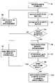
- FIG. 1shows a block diagram of a buffer chip according to one embodiment of the invention.
- FIG. 2shows a flowchart to illustrating one embodiment of the inventive method.
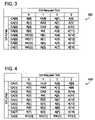
- FIG. 3shows a command protocol for actuating a buffer chip according to one embodiment of the invention.
- FIG. 4shows another command protocol for a buffer chip according to another embodiment of the invention.
- FIG. 5shows a data protocol for a buffer chip according to one embodiment of the invention.
- FIG. 6shows another data protocol for a buffer chip according to another embodiment of the invention.
- FIG. 1shows a buffer chip 1 according to one embodiment of the invention.
- the buffer chip 1has a first data interface 2 for receiving command data and for transferring data which have been read from one of the memory arrangements 3 to a memory controller 4 or to further buffer chips.
- the first data interface 2is able to receive data which are to be written and is able to write these data to the respectively addressed memory arrangement 3 . Reading from the memory arrangements 3 or writing to the memory arrangements 3 is performed via a second data interface 5 .
- the memory arrangements 3may be connected to the second data interface 5 by means of separate data lines. Alternatively, the memory arrangements 3 may be connected to the buffer chip 1 by means of a common data bus via the second data interface 5 .
- the buffer chips 1may be connected to the memory controller 4 in the form of a daisychain (i.e., merely point-to-point connections between memory controller 4 and the first buffer chip 1 and between the first buffer chip and a second buffer chip). In one embodiment, there is no common data bus via which all of the data are transferred between buffer chips 1 and memory controller 4 .
- a data bus 6 having a P2P data linkallows faster transfer of data, since the line capacities are lower.
- the result of the faster transfer of datais that fewer data lines are necessary from the memory controller 4 to the buffer chips 1 , which means that it is easier to provide identical data line lengths for the data bus 6 in the layout.
- Identical data line lengthshave the advantage that faster signals can be transferred, since the propagation times on all the data lines are then identical.
- the data bus 6may be used to transfer command data and memory data.
- the command datamay specify the address of the memory arrangement 3 , of the memory bank and also of the memory location to which memory data are to be written or from which memory data are to be read.
- the memory controller 4may send a command data item, which is received by the first data interface 2 and analyzed in a switching device 7 .
- the switching device 7decides whether one of the memory arrangements 3 connected to the respective buffer chip 1 needs to be addressed.
- the command data and/or the memory dataare parallelized in a conversion unit 8 , so that the data available have the necessary data width and speed for the memory arrangements 3 . If none of the memory arrangements 3 connected to the respective buffer chip 1 need to be addressed, then the switching device 7 forwards the received command data item and/or the received memory data item via the first data interface 2 to a subsequent buffer chip 1 . The forwarded command data item and/or memory data item are received by the respective first data interface 2 on the next buffer chip 1 and processed by the switching device 7 respectively.
- the conversion unit 8may be connected to a buffer storage 9 which comprises a write buffer storage 10 and a read buffer storage 11 .
- the write buffer storage 10is used for initially buffer-storing a memory data item which is to be written before the memory data item is written to the respective addressed memory arrangement 3 via the second data interface 5 .
- the read buffer storage 11has the function of buffer-storing a memory data item which has been read from the respectively addressed memory arrangement 3 via the second data interface 5 , before the memory data item is output to the memory controller 4 via the conversion unit 8 and the first data interface 2 .
- data busesmay be in either bidirectional or unidirectional form.
- the buffer storage 9is used to buffer a data item to accommodate different bus turnaround times from a write operation to a read operation or from a read operation to a write operation. Particularly when changing from a write operation to a read operation, access to the same memory arrangement 3 requires a high latency before the last writing of a memory data item to the memory arrangement can be followed by reading of a memory data item from the same memory arrangement 3 . This latency is prescribed by the parameters of the memory chips (TWR and TWTR) provided in the memory arrangement 3 .
- the latencyis usually made for the latency to be high enough for the maximum required latency not to be undershot during all possible memory access operations, regardless of the type of access. The result of this is that, for many memory access operations, higher latency is provided than would be necessary.
- the memory controller 4may be provided to ascertain the associated latency on the basis of the type of memory access and to send the command data with an appropriate delay. This would noticeably increase the complexity of the circuits in the memory controller 4 .
- the buffer storage 9 in the buffer chip 1allows the memory controller 4 to be provided at a low complexity level, since the buffer storage 9 , particularly the write buffer storage 10 , is able to hide the latency required for a bus turnaround from a write operation to a read operation for the same memory arrangement 3 .
- the buffer storage 9works as follows. Data are written via the data bus 6 and the buffer chip 1 to the memory arrangement 3 according to a write command and the subsequent one or more memory data items. Before the memory data are written to the memory arrangement addressed by the command data item, the memory data are first stored in the write buffer storage 10 . If the data bus 6 is used to send the buffer chip 1 a command data item which contains a read command for reading a data item from the same memory arrangement 3 , then the last memory data item to be written in the write buffer storage 10 is not output to the memory arrangement 3 in question via the second data interface 5 . Instead, the read command received is immediately forwarded to the addressed memory arrangement 3 , and the requested data are read via the read buffer storage 11 via the data bus 6 .
- the control unit 12decides, on the basis of the received command data, whether the write data item stored in the write buffer storage 10 needs to be written to the addressed memory arrangement 3 . As soon as the control unit 12 detects a read command, a check is carried out to determine whether the read command relates to the same memory arrangement 3 as the write operations performed previously. If the read command does relate to the same memory arrangement 3 , then the writing of the write data to the memory arrangement 3 is stopped and the read command is immediately forwarded to the memory arrangement 3 in question.
- the read commandrelates to another memory arrangement 3
- the writing of the write data to the memory arrangement 3 in questioncan be continued and the read command can be forwarded to the other memory arrangement 3 addressed by the read command in order to start reading the data.
- thisis possible only when the memory arrangements 3 are connected to the second data interface 5 by means of separate data lines. If the memory arrangements 3 are connected to the buffer chip by means of a common data bus, then the latter variant does not apply.
- the memory data item stored in the write buffer storageis written when access to the memory arrangement 3 in question is interrupted, i.e., the reading of data from the memory arrangement is first ended.
- the time in which there is no access to the memory arrangement 3 in questionis used in order to empty the write buffer storage 10 by storing the data stored therein in the memory arrangement 3 .
- the memory data stored in the write buffer storage 10are written to the memory arrangement 3 when write access to the memory arrangement 3 in question is started again. This serves to empty the write buffer storage 10 as quickly as possible, so that it is possible to buffer-store new write data arriving.
- the control unit 12can also provide for the reading of memory data from the addressed memory arrangement 3 to involve only some of the memory data which have been read and are stored in the read buffer storage 11 being sent to the memory controller 4 via the data bus 6 . This is appropriate since, in future memory architectures with burst access to memory chips in the memory arrangement 3 , too great a volume of data may be provided which cannot be picked up simultaneously by a microprocessor connected to the memory controller 4 .
- the minimum burst lengthi.e. the minimum volume of data which are written or read with a command
- the prefetch ratiois dependent on the “prefetch ratio”. While the prefetch ratio is 2 in DDR memory chips and the prefetch ratio is 4 in DDR-II memory chips, the prefetch ratio may be 8 for the coming generation of DDR-III memory chips.
- the minimum burst lengthwould only be 4 for DDR-III memory chips as well. The reason for this is that the volume of data which are transferred to the microprocessor upon a read command will probably be 64 bytes. If two 8-byte data buses are operated in parallel or in interleaved fashion, then the volume of data which are transferred for a minimum burst length of 8 is 128 bytes. For this reason, it would be desirable to limit the minimum burst length to 4.
- the read buffer storage 11can buffer-store the data from the memory arrangements in line with a burst length of 8 bits, with the control unit 12 respectively forwarding just a portion, namely half, of the buffer-stored memory data to the conversion unit 8 for output to the first data interface 2 and then the memory controller 4 .
- the memory controller 4receives only that volume of data which the connected microprocessor requires, even in memory arrangements having memory chips which have a minimum burst length of more than 4 bits.
- the data which have been read initiallyremain in the read buffer storage 11 , so that a suitable read command is able to transfer the remaining data directly from the read buffer storage 11 to the memory controller 4 without the buffer chip 1 sending a fresh read command to the memory arrangement 3 .
- FIG. 2shows a flowchart to illustrating a method 200 according to one embodiment of the invention.
- the method 200relates to the sequence in a buffer chip according to one embodiment of the invention.
- a write commandis received by the buffer chip 1 , specifying that data which are to be written can now be received via the data bus.
- the data which are to be writtenare received in a step S 2 and are first buffer-stored in a step S 3 .
- a step S 4a check is then carried out to determine whether a read command for reading the same memory arrangement has been received. If no read command has been received, the buffer-stored data item is written to the addressed memory arrangement in question in a step S 5 , and execution returns to step S 2 .
- step S 6If a read command for the same memory arrangement has been received, then in a step S 6 the addressed memory area in the memory arrangement in question is addressed, and the corresponding read data are received.
- the buffer-stored data to be writtenare not yet written.
- the read data received from the addressed memory arrangementare buffer-stored in a step S 7 , and a check is then carried out in a step S 8 to determine whether further data need to be read from the addressed memory arrangement. If further read data from the memory arrangement have been requested, the buffer-stored read data are sent to the memory controller in a step S 9 , and execution returns to step S 6 .
- the read data(buffer-stored) are output to the memory controller, and the data to be written which were buffer-stored and have not yet been written to the memory arrangement in question, are written to the memory arrangement (step S 10 ).
- the buffer storage 9 described above and the associated control unit 12may also be provided in more complex form.
- a read/write cache functionalitycan be implemented in the buffer chip 1 , which not only allows the problems described above to be solved but additionally allows the overall performance of the entire system to be increased. Since, in contrast to the memory chips in the memory arrangement 3 , the buffer chip 1 may use a production technology which allows fast logic circuits, and complex cache control circuits may be conceivable in the buffer chip 1 .
- Such a complex cache control circuitis able, for example on the basis of the read and write commands and the address ranges used in the system, to request various memory data which are to be read from the memory chips in the memory arrangement 3 in advance in order to provide the requested data from the buffer storage 9 very quickly in the event of a read command from the memory controller 4 .
- a fundamental featureis that the execution time for various read or write commands can vary greatly depending on whether the data are handled via the buffer storage 9 or via the cache memory in the buffer chips 1 , or whether the read or write commands need to be executed by the memory chips. It is therefore possible to provide a command and user data protocol which allows the data for the individual read and write commands to be transferred in a different order than is prescribed by the commands.
- an “identification number”may be transferred with the command data item and with the memory data item and may be used to identify associated command data and memory data.
- FIG. 3shows a command protocol 300 for actuating a buffer chip according to one embodiment of the invention.
- the data lines CA ( 0 to 7 ) in the data bus 6transfer a command data item in four sections, i.e., the “ticks”.
- the memory arrangement address R( 0 ) to R( 3 )is transferred on the four data bus lines CA 0 to CA 3 .
- the identification number RID( 0 ) to RID( 3 )is transferred in order to be able to associate the command data item with a corresponding memory data item.
- ticksare used to transfer address data for the memory chips in the memory arrangements, the bank address and also the actuation commands, row activation signal RAS, column activation signal CAS, write signal WE.
- the second tickis used to transfer a bit which indicates whether the command data item is intended to address a memory chip or memory arrangement, or whether the command data item is a command for the buffer chip 1 .
- FIG. 4shows another command protocol 400 for a buffer chip according to another embodiment of the invention.
- a further data bus line CA( 8 )is provided in order to transfer 4 bits of the identification number RID( 0 to 3 ) in the four ticks.
- FIG. 5shows a data protocol 500 for a buffer chip according to one embodiment of the invention.
- the memory data itemis transferred in four ticks having a width of 16 data bits DQ 0 to DQ 15 .
- the first four data bits in the first tickcarry the identification number RID( 0 to 3 ).
- FIG. 6shows another data protocol 600 for a buffer chip according to another embodiment of the invention, where the data bus 6 comprises a further data bus line DQ( 16 ). On the further data bus line DQ( 16 ), four ticks are used to transfer the 4 bits of the identification number, so that it is possible to make an association with the respective command data item having the same identification number.
- identification numbersallows the data for the individual write commands and read commands to be transferred in a different order from and to the memory controller 4 than the command data.
- the buffer storage 9is arranged between the conversion unit 8 and the second data interface 5 .
- the buffer storage 9may be arranged between the conversion unit 8 and the switching device 7 or between the first data interface 2 and the switching device 7 .
- the buffer chip 1 and the connected memory arrangement 3may be combined in “memory modules” and may be physically integrated in a “DIMM module”. DIMM modules are typically memory configurations used in personal computers.
Landscapes
- Engineering & Computer Science (AREA)
- Theoretical Computer Science (AREA)
- Physics & Mathematics (AREA)
- General Engineering & Computer Science (AREA)
- General Physics & Mathematics (AREA)
- Memory System Of A Hierarchy Structure (AREA)
- Memory System (AREA)
Abstract
Description
Claims (20)
Applications Claiming Priority (2)
| Application Number | Priority Date | Filing Date | Title |
|---|---|---|---|
| DE10309919ADE10309919B4 (en) | 2003-03-07 | 2003-03-07 | Buffer block and memory modules |
| DE10309919.0-53 | 2003-03-07 |
Publications (2)
| Publication Number | Publication Date |
|---|---|
| US20040228166A1 US20040228166A1 (en) | 2004-11-18 |
| US7447805B2true US7447805B2 (en) | 2008-11-04 |
Family
ID=32891923
Family Applications (1)
| Application Number | Title | Priority Date | Filing Date |
|---|---|---|---|
| US10/792,408Expired - Fee RelatedUS7447805B2 (en) | 2003-03-07 | 2004-03-03 | Buffer chip and method for controlling one or more memory arrangements |
Country Status (3)
| Country | Link |
|---|---|
| US (1) | US7447805B2 (en) |
| CN (1) | CN1289998C (en) |
| DE (1) | DE10309919B4 (en) |
Cited By (8)
| Publication number | Priority date | Publication date | Assignee | Title |
|---|---|---|---|---|
| US20060227627A1 (en)* | 2005-03-03 | 2006-10-12 | Georg Braun | Buffer component for a memory module, and a memory module and a memory system having such buffer component |
| US20080222330A1 (en)* | 2007-03-08 | 2008-09-11 | Ricoh Company, Limited | Semiconductor integrated circuit and image processing apparatus having the same |
| US20090193167A1 (en)* | 2008-01-25 | 2009-07-30 | Realtek Semiconductor Corp. | Arbitration device and method |
| US7730244B1 (en)* | 2008-03-27 | 2010-06-01 | Xilinx, Inc. | Translation of commands in an interconnection of an embedded processor block core in an integrated circuit |
| US20100165780A1 (en)* | 2008-12-27 | 2010-07-01 | Bains Kuljit S | Dynamic random access memory with shadow writes |
| US10248330B2 (en) | 2017-05-30 | 2019-04-02 | Seagate Technology Llc | Data storage device with buffer tenure management |
| US11429547B2 (en)* | 2019-11-22 | 2022-08-30 | Wago Verwaltungsgesellschaft Mbh | Apparatus and method for the buffered transmission of data by a controller to reduce a load on a central processing unit |
| US20240069763A1 (en)* | 2021-02-25 | 2024-02-29 | Sony Semiconductor Solutions Corporation | Memory controller and memory access method |
Families Citing this family (46)
| Publication number | Priority date | Publication date | Assignee | Title |
|---|---|---|---|---|
| US8796830B1 (en) | 2006-09-01 | 2014-08-05 | Google Inc. | Stackable low-profile lead frame package |
| US8090897B2 (en) | 2006-07-31 | 2012-01-03 | Google Inc. | System and method for simulating an aspect of a memory circuit |
| US8359187B2 (en) | 2005-06-24 | 2013-01-22 | Google Inc. | Simulating a different number of memory circuit devices |
| US8089795B2 (en) | 2006-02-09 | 2012-01-03 | Google Inc. | Memory module with memory stack and interface with enhanced capabilities |
| US20080082763A1 (en) | 2006-10-02 | 2008-04-03 | Metaram, Inc. | Apparatus and method for power management of memory circuits by a system or component thereof |
| US8041881B2 (en) | 2006-07-31 | 2011-10-18 | Google Inc. | Memory device with emulated characteristics |
| US8060774B2 (en) | 2005-06-24 | 2011-11-15 | Google Inc. | Memory systems and memory modules |
| US7386656B2 (en) | 2006-07-31 | 2008-06-10 | Metaram, Inc. | Interface circuit system and method for performing power management operations in conjunction with only a portion of a memory circuit |
| US8081474B1 (en) | 2007-12-18 | 2011-12-20 | Google Inc. | Embossed heat spreader |
| US7590796B2 (en) | 2006-07-31 | 2009-09-15 | Metaram, Inc. | System and method for power management in memory systems |
| US7609567B2 (en) | 2005-06-24 | 2009-10-27 | Metaram, Inc. | System and method for simulating an aspect of a memory circuit |
| US8055833B2 (en) | 2006-10-05 | 2011-11-08 | Google Inc. | System and method for increasing capacity, performance, and flexibility of flash storage |
| US8386722B1 (en) | 2008-06-23 | 2013-02-26 | Google Inc. | Stacked DIMM memory interface |
| US9171585B2 (en) | 2005-06-24 | 2015-10-27 | Google Inc. | Configurable memory circuit system and method |
| US8438328B2 (en) | 2008-02-21 | 2013-05-07 | Google Inc. | Emulation of abstracted DIMMs using abstracted DRAMs |
| US7392338B2 (en) | 2006-07-31 | 2008-06-24 | Metaram, Inc. | Interface circuit system and method for autonomously performing power management operations in conjunction with a plurality of memory circuits |
| US8111566B1 (en) | 2007-11-16 | 2012-02-07 | Google, Inc. | Optimal channel design for memory devices for providing a high-speed memory interface |
| US7580312B2 (en) | 2006-07-31 | 2009-08-25 | Metaram, Inc. | Power saving system and method for use with a plurality of memory circuits |
| US7472220B2 (en) | 2006-07-31 | 2008-12-30 | Metaram, Inc. | Interface circuit system and method for performing power management operations utilizing power management signals |
| US9507739B2 (en) | 2005-06-24 | 2016-11-29 | Google Inc. | Configurable memory circuit system and method |
| US8077535B2 (en) | 2006-07-31 | 2011-12-13 | Google Inc. | Memory refresh apparatus and method |
| US8244971B2 (en) | 2006-07-31 | 2012-08-14 | Google Inc. | Memory circuit system and method |
| US8327104B2 (en) | 2006-07-31 | 2012-12-04 | Google Inc. | Adjusting the timing of signals associated with a memory system |
| US8397013B1 (en) | 2006-10-05 | 2013-03-12 | Google Inc. | Hybrid memory module |
| US9542352B2 (en) | 2006-02-09 | 2017-01-10 | Google Inc. | System and method for reducing command scheduling constraints of memory circuits |
| US20080028136A1 (en) | 2006-07-31 | 2008-01-31 | Schakel Keith R | Method and apparatus for refresh management of memory modules |
| US10013371B2 (en) | 2005-06-24 | 2018-07-03 | Google Llc | Configurable memory circuit system and method |
| US8335894B1 (en) | 2008-07-25 | 2012-12-18 | Google Inc. | Configurable memory system with interface circuit |
| US8130560B1 (en) | 2006-11-13 | 2012-03-06 | Google Inc. | Multi-rank partial width memory modules |
| KR101377305B1 (en) | 2005-06-24 | 2014-03-25 | 구글 인코포레이티드 | An integrated memory core and memory interface circuit |
| WO2007028109A2 (en) | 2005-09-02 | 2007-03-08 | Metaram, Inc. | Methods and apparatus of stacking drams |
| US7991965B2 (en) | 2006-02-07 | 2011-08-02 | Intel Corporation | Technique for using memory attributes |
| US9632929B2 (en) | 2006-02-09 | 2017-04-25 | Google Inc. | Translating an address associated with a command communicated between a system and memory circuits |
| US7724589B2 (en) | 2006-07-31 | 2010-05-25 | Google Inc. | System and method for delaying a signal communicated from a system to at least one of a plurality of memory circuits |
| JP4470183B2 (en)* | 2006-08-28 | 2010-06-02 | エルピーダメモリ株式会社 | Semiconductor memory device |
| US7610448B2 (en) | 2006-12-27 | 2009-10-27 | Intel Corporation | Obscuring memory access patterns |
| US7921243B1 (en)* | 2007-01-05 | 2011-04-05 | Marvell International Ltd. | System and method for a DDR SDRAM controller |
| US8209479B2 (en) | 2007-07-18 | 2012-06-26 | Google Inc. | Memory circuit system and method |
| US8080874B1 (en) | 2007-09-14 | 2011-12-20 | Google Inc. | Providing additional space between an integrated circuit and a circuit board for positioning a component therebetween |
| US20090150894A1 (en)* | 2007-12-10 | 2009-06-11 | Ming Huang | Nonvolatile memory (NVM) based solid-state disk (SSD) system for scaling and quality of service (QoS) by parallelizing command execution |
| US9110597B2 (en)* | 2007-12-10 | 2015-08-18 | Hewlett-Packard Development Company, L.P. | Data processing method and system |
| DE202010017690U1 (en) | 2009-06-09 | 2012-05-29 | Google, Inc. | Programming dimming terminating resistor values |
| KR101796116B1 (en) | 2010-10-20 | 2017-11-10 | 삼성전자 주식회사 | Semiconductor device, memory module and memory system having the same and operating method thereof |
| KR20180114417A (en)* | 2017-04-10 | 2018-10-18 | 에스케이하이닉스 주식회사 | Controller and operating method thereof |
| US12189989B2 (en)* | 2017-09-20 | 2025-01-07 | SK Hynix Inc. | Memory device queuing a plurality of commands and memory system having memory device |
| TWI766764B (en)* | 2021-07-20 | 2022-06-01 | 群聯電子股份有限公司 | Method for managing memory buffer, memory control circuit unit and memory storage apparatus |
Citations (13)
| Publication number | Priority date | Publication date | Assignee | Title |
|---|---|---|---|---|
| US4792926A (en)* | 1985-12-09 | 1988-12-20 | Kabushiki Kaisha Toshiba | High speed memory system for use with a control bus bearing contiguous segmentially intermixed data read and data write request signals |
| US5745791A (en)* | 1992-09-16 | 1998-04-28 | Intel Corporation | System for interfacing first and second components having different data path width by generating first and second component address to read data into buffer |
| US5787481A (en) | 1994-03-24 | 1998-07-28 | Texas Instruments Incorporated | System for managing write and/or read access priorities between central processor and memory operationally connected |
| US6144616A (en)* | 1998-10-30 | 2000-11-07 | Fujitsu Limited | Semiconductor memory device |
| US20010052057A1 (en) | 2000-06-12 | 2001-12-13 | Jiin Lai | Buffer for varying data access speed and system applying the same |
| US6343352B1 (en)* | 1997-10-10 | 2002-01-29 | Rambus Inc. | Method and apparatus for two step memory write operations |
| US6430649B1 (en)* | 1999-06-07 | 2002-08-06 | Sun Microsystems, Inc. | Method and apparatus for enforcing memory reference dependencies through a load store unit |
| DE10210904A1 (en) | 2001-03-06 | 2003-01-16 | Samsung Electronics Co Ltd | Memory module, associated memory system and clock signal generation method |
| US6530006B1 (en)* | 2000-09-18 | 2003-03-04 | Intel Corporation | System and method for providing reliable transmission in a buffered memory system |
| US6622224B1 (en)* | 1997-12-29 | 2003-09-16 | Micron Technology, Inc. | Internal buffered bus for a drum |
| US6622227B2 (en)* | 2000-12-27 | 2003-09-16 | Intel Corporation | Method and apparatus for utilizing write buffers in memory control/interface |
| US6640292B1 (en)* | 1999-09-10 | 2003-10-28 | Rambus Inc. | System and method for controlling retire buffer operation in a memory system |
| US6877077B2 (en)* | 2001-12-07 | 2005-04-05 | Sun Microsystems, Inc. | Memory controller and method using read and write queues and an ordering queue for dispatching read and write memory requests out of order to reduce memory latency |
- 2003
- 2003-03-07DEDE10309919Apatent/DE10309919B4/ennot_activeExpired - Fee Related
- 2004
- 2004-03-03USUS10/792,408patent/US7447805B2/ennot_activeExpired - Fee Related
- 2004-03-05CNCNB2004100080144Apatent/CN1289998C/ennot_activeExpired - Fee Related
Patent Citations (14)
| Publication number | Priority date | Publication date | Assignee | Title |
|---|---|---|---|---|
| US4792926A (en)* | 1985-12-09 | 1988-12-20 | Kabushiki Kaisha Toshiba | High speed memory system for use with a control bus bearing contiguous segmentially intermixed data read and data write request signals |
| US5745791A (en)* | 1992-09-16 | 1998-04-28 | Intel Corporation | System for interfacing first and second components having different data path width by generating first and second component address to read data into buffer |
| US5787481A (en) | 1994-03-24 | 1998-07-28 | Texas Instruments Incorporated | System for managing write and/or read access priorities between central processor and memory operationally connected |
| US6343352B1 (en)* | 1997-10-10 | 2002-01-29 | Rambus Inc. | Method and apparatus for two step memory write operations |
| US6622224B1 (en)* | 1997-12-29 | 2003-09-16 | Micron Technology, Inc. | Internal buffered bus for a drum |
| US6144616A (en)* | 1998-10-30 | 2000-11-07 | Fujitsu Limited | Semiconductor memory device |
| US6430649B1 (en)* | 1999-06-07 | 2002-08-06 | Sun Microsystems, Inc. | Method and apparatus for enforcing memory reference dependencies through a load store unit |
| US6640292B1 (en)* | 1999-09-10 | 2003-10-28 | Rambus Inc. | System and method for controlling retire buffer operation in a memory system |
| US20010052057A1 (en) | 2000-06-12 | 2001-12-13 | Jiin Lai | Buffer for varying data access speed and system applying the same |
| US6530006B1 (en)* | 2000-09-18 | 2003-03-04 | Intel Corporation | System and method for providing reliable transmission in a buffered memory system |
| US6622227B2 (en)* | 2000-12-27 | 2003-09-16 | Intel Corporation | Method and apparatus for utilizing write buffers in memory control/interface |
| DE10210904A1 (en) | 2001-03-06 | 2003-01-16 | Samsung Electronics Co Ltd | Memory module, associated memory system and clock signal generation method |
| US6877079B2 (en) | 2001-03-06 | 2005-04-05 | Samsung Electronics Co., Ltd. | Memory system having point-to-point bus configuration |
| US6877077B2 (en)* | 2001-12-07 | 2005-04-05 | Sun Microsystems, Inc. | Memory controller and method using read and write queues and an ordering queue for dispatching read and write memory requests out of order to reduce memory latency |
Cited By (12)
| Publication number | Priority date | Publication date | Assignee | Title |
|---|---|---|---|---|
| US20060227627A1 (en)* | 2005-03-03 | 2006-10-12 | Georg Braun | Buffer component for a memory module, and a memory module and a memory system having such buffer component |
| US7646650B2 (en)* | 2005-03-03 | 2010-01-12 | Infineon Technologies Ag | Buffer component for a memory module, and a memory module and a memory system having such buffer component |
| US20080222330A1 (en)* | 2007-03-08 | 2008-09-11 | Ricoh Company, Limited | Semiconductor integrated circuit and image processing apparatus having the same |
| US7702841B2 (en)* | 2007-03-08 | 2010-04-20 | Ricoh Company, Limited | Semiconductor integrated circuit and image processing apparatus having the same |
| US20090193167A1 (en)* | 2008-01-25 | 2009-07-30 | Realtek Semiconductor Corp. | Arbitration device and method |
| US8180942B2 (en)* | 2008-01-25 | 2012-05-15 | Realtek Semiconductor Corp. | Arbitration device and method |
| US7730244B1 (en)* | 2008-03-27 | 2010-06-01 | Xilinx, Inc. | Translation of commands in an interconnection of an embedded processor block core in an integrated circuit |
| US20100165780A1 (en)* | 2008-12-27 | 2010-07-01 | Bains Kuljit S | Dynamic random access memory with shadow writes |
| US8281101B2 (en)* | 2008-12-27 | 2012-10-02 | Intel Corporation | Dynamic random access memory with shadow writes |
| US10248330B2 (en) | 2017-05-30 | 2019-04-02 | Seagate Technology Llc | Data storage device with buffer tenure management |
| US11429547B2 (en)* | 2019-11-22 | 2022-08-30 | Wago Verwaltungsgesellschaft Mbh | Apparatus and method for the buffered transmission of data by a controller to reduce a load on a central processing unit |
| US20240069763A1 (en)* | 2021-02-25 | 2024-02-29 | Sony Semiconductor Solutions Corporation | Memory controller and memory access method |
Also Published As
| Publication number | Publication date |
|---|---|
| CN1530819A (en) | 2004-09-22 |
| DE10309919B4 (en) | 2008-09-25 |
| CN1289998C (en) | 2006-12-13 |
| DE10309919A1 (en) | 2004-09-23 |
| US20040228166A1 (en) | 2004-11-18 |
Similar Documents
| Publication | Publication Date | Title |
|---|---|---|
| US7447805B2 (en) | Buffer chip and method for controlling one or more memory arrangements | |
| US7907469B2 (en) | Multi-port memory device for buffering between hosts and non-volatile memory devices | |
| US6795899B2 (en) | Memory system with burst length shorter than prefetch length | |
| CN1952868A (en) | Memory module, memory system and method for controlling thereof | |
| US7464231B2 (en) | Method for self-timed data ordering for multi-data rate memories | |
| US20110289269A1 (en) | Memory system and method having point-to-point link | |
| JP4199658B2 (en) | Memory device performing addressing with different burst order in read and write operations | |
| JP2007073052A (en) | Accessing external memory from integrated circuit | |
| US12001682B2 (en) | PIM computing system and memory controller thereof | |
| US7840744B2 (en) | Rank select operation between an XIO interface and a double data rate interface | |
| US9741406B2 (en) | Semiconductor memory and memory system | |
| US5926828A (en) | Method and apparatus for controlling data transfer between a synchronous DRAM-type memory and a system bus | |
| US5969997A (en) | Narrow data width DRAM with low latency page-hit operations | |
| JP4707351B2 (en) | Multi-bank memory scheduling method | |
| JP2004127305A (en) | Memory controller | |
| US8074096B2 (en) | Semiconductor integrated circuit, memory system, memory controller and memory control method | |
| US6751130B2 (en) | Integrated memory device, method of operating an integrated memory, and memory system having a plurality of integrated memories | |
| US11983411B2 (en) | Methods, devices and systems for including alternate memory access operations over memory interface | |
| US20220107908A1 (en) | Methods, devices and systems for high speed transactions with nonvolatile memory on a double data rate memory bus | |
| JP2001028186A (en) | Semiconductor memory, access method for it, and data processing system | |
| HK1068181B (en) | Memory system with burst length shorter than prefetch length | |
| KR20020011018A (en) | Method for high speed wrire operating in semiconductor memory device |
Legal Events
| Date | Code | Title | Description |
|---|---|---|---|
| AS | Assignment | Owner name:INFINEON TECHNOLOGIES AG, GERMANY Free format text:ASSIGNMENT OF ASSIGNORS INTEREST;ASSIGNORS:BRAUN, GEORGE;RUCKERBAUER, HERMANN;REEL/FRAME:014891/0675;SIGNING DATES FROM 20040421 TO 20040622 | |
| STCF | Information on status: patent grant | Free format text:PATENTED CASE | |
| FEPP | Fee payment procedure | Free format text:PAYER NUMBER DE-ASSIGNED (ORIGINAL EVENT CODE: RMPN); ENTITY STATUS OF PATENT OWNER: LARGE ENTITY Free format text:PAYOR NUMBER ASSIGNED (ORIGINAL EVENT CODE: ASPN); ENTITY STATUS OF PATENT OWNER: LARGE ENTITY | |
| AS | Assignment | Owner name:QIMONDA AG, GERMANY Free format text:ASSIGNMENT OF ASSIGNORS INTEREST;ASSIGNOR:INFINEON TECHNOLOGIES AG;REEL/FRAME:023821/0535 Effective date:20060425 Owner name:QIMONDA AG,GERMANY Free format text:ASSIGNMENT OF ASSIGNORS INTEREST;ASSIGNOR:INFINEON TECHNOLOGIES AG;REEL/FRAME:023821/0535 Effective date:20060425 | |
| FPAY | Fee payment | Year of fee payment:4 | |
| AS | Assignment | Owner name:INFINEON TECHNOLOGIES AG, GERMANY Free format text:ASSIGNMENT OF ASSIGNORS INTEREST;ASSIGNOR:QIMONDA AG;REEL/FRAME:035623/0001 Effective date:20141009 | |
| AS | Assignment | Owner name:POLARIS INNOVATIONS LIMITED, IRELAND Free format text:ASSIGNMENT OF ASSIGNORS INTEREST;ASSIGNOR:INFINEON TECHNOLOGIES AG;REEL/FRAME:036873/0758 Effective date:20150708 | |
| FPAY | Fee payment | Year of fee payment:8 | |
| SULP | Surcharge for late payment | Year of fee payment:7 | |
| FEPP | Fee payment procedure | Free format text:MAINTENANCE FEE REMINDER MAILED (ORIGINAL EVENT CODE: REM.); ENTITY STATUS OF PATENT OWNER: LARGE ENTITY | |
| LAPS | Lapse for failure to pay maintenance fees | Free format text:PATENT EXPIRED FOR FAILURE TO PAY MAINTENANCE FEES (ORIGINAL EVENT CODE: EXP.); ENTITY STATUS OF PATENT OWNER: LARGE ENTITY | |
| STCH | Information on status: patent discontinuation | Free format text:PATENT EXPIRED DUE TO NONPAYMENT OF MAINTENANCE FEES UNDER 37 CFR 1.362 | |
| FP | Lapsed due to failure to pay maintenance fee | Effective date:20201104 |