US7447240B2 - Method and system for synchronizing communications links in a hub-based memory system - Google Patents
Method and system for synchronizing communications links in a hub-based memory systemDownload PDFInfo
- Publication number
- US7447240B2 US7447240B2US10/813,040US81304004AUS7447240B2US 7447240 B2US7447240 B2US 7447240B2US 81304004 AUS81304004 AUS 81304004AUS 7447240 B2US7447240 B2US 7447240B2
- Authority
- US
- United States
- Prior art keywords
- enablement
- operable
- memory
- downstream
- upstream
- Prior art date
- Legal status (The legal status is an assumption and is not a legal conclusion. Google has not performed a legal analysis and makes no representation as to the accuracy of the status listed.)
- Active, expires
Links
Images


Classifications
- G—PHYSICS
- G06—COMPUTING OR CALCULATING; COUNTING
- G06F—ELECTRIC DIGITAL DATA PROCESSING
- G06F13/00—Interconnection of, or transfer of information or other signals between, memories, input/output devices or central processing units
- G06F13/14—Handling requests for interconnection or transfer
- G06F13/16—Handling requests for interconnection or transfer for access to memory bus
- G06F13/1668—Details of memory controller
- G06F13/1684—Details of memory controller using multiple buses
- G—PHYSICS
- G06—COMPUTING OR CALCULATING; COUNTING
- G06F—ELECTRIC DIGITAL DATA PROCESSING
- G06F13/00—Interconnection of, or transfer of information or other signals between, memories, input/output devices or central processing units
- G06F13/14—Handling requests for interconnection or transfer
- G06F13/16—Handling requests for interconnection or transfer for access to memory bus
- G06F13/1668—Details of memory controller
- G06F13/1689—Synchronisation and timing concerns
Definitions
- This inventionrelates to computer systems, and, more particularly, to a computer system including a system memory having a memory hub architecture.
- a system controller or memory controlleris coupled over a high speed link to several memory modules.
- the memory modulesare coupled in a point-to-point or daisy chain architecture such that the memory modules are connected one to another in series.
- the memory controlleris coupled to a first memory module over a first high speed link, with the first memory module connected to a second memory module through a second high speed link, and the second memory module coupled to a third memory module through a third high speed link, and so on in a daisy chain fashion.
- Each memory moduleincludes a memory hub that is coupled to the corresponding high speed links and a number of memory devices on the module, with the memory hubs efficiently routing memory requests and memory responses between the controller and the memory devices over the high speed links.
- Computer systems employing this architecturecan have a higher bandwidth because a processor can access one memory device while another memory device is responding to a prior memory access. For example, the processor can output write data to one of the memory devices in the system while another memory device in the system is preparing to provide read data to the processor.
- this architecturealso provides for easy expansion of the system memory without concern for degradation in signal quality as more memory modules are added, such as occurs in conventional multi drop bus architectures.
- Signalsare transferred over the high speed links at very high rates, with the links being optical, radio frequency, or other suitable high speed communications media.
- the duration for which each signal being transferred over the high speed link is validdecreases by a corresponding amount, as will be understood by one skilled in the art.
- the data window or “data eye” for each of the signalsdecreases as the data transfer rate increases.
- the data eye for each of the signalsdefines the actual duration for which each signal is valid after timing skew, jitter, duty cycle variation, and other types of unwanted signal distortion are considered.
- Signal distortioncan arise from a variety of sources, such as different loading on the lines of the link and the physical lengths of such lines.
- a conventional system memoryto synchronize memory devices coupled to a memory controller the controller enters an initialization or synchronization mode of operation and applies a test data pattern to the memory devices. Typically, the controller thereafter adjusts the phase of the data strobe signal relative to the signals forming the test data pattern and determines limits for phase shifts of the data strobe signal that allow the memory device to successfully capture the data signals. A phase shift within the determined limits is then selected for use during normal operation of the controller and memory device.
- each memory deviceis coupled to the controller over a common memory bus.
- a memory hub system having a daisy-chain configurationnot every memory hub is coupled directly to the controller. The controller does not directly communicate with each memory hub in a memory hub system having more than one memory hub, and therefore the controller cannot synchronize the memory hubs in the same way as in a conventional system memory.
- a methodfor synchronizing communications links in a memory hub system.
- the memory hub systemincludes a system controller and a plurality of memory hubs coupled in series, with pairs of downstream and upstream links being coupled between adjacent modules and the controller.
- the methodincludes synchronizing each upstream and downstream link. In a clockwise order starting with the downstream link coupled between the controller and the first memory module, the next adjacent clockwise link is signaled that the prior clockwise link has been synchronized.
- the methoddetects through the upstream link coupled between the controller and the first memory module when all links have been synchronized.
- each linkis enabled.
- the methoddetects through the upstream link coupled between the controller and the first memory module when all links have been enabled.
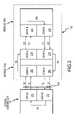
- FIG. 1is a block diagram of a computer system including a system memory having a high-bandwidth memory hub architecture according to one example of the present invention.
- FIG. 2is a block diagram illustrating in more detail the memory hubs contained in the memory modules in the system memory of FIG. 1 according to one example of the present invention.
- FIG. 3is a functional diagram illustrating the operation of the system controller and the memory modules of FIG. 2 during an initialization stage of a synchronization process according to one embodiment of the present invention.
- FIG. 4is a functional diagram illustrating the operation of the system controller and memory modules of FIG. 2 during an enablement stage of a synchronization process according to one embodiment of the present invention.
- FIG. 1A computer system 100 according to one example of the present invention is shown in FIG. 1 .
- the computer system 100includes a system memory 102 having a memory hub architecture that executes an initialization or synchronization process to synchronize a plurality of memory hubs 140 contained in a plurality of memory modules 130 , as will be explained in more detail below.
- a system memory 102having a memory hub architecture that executes an initialization or synchronization process to synchronize a plurality of memory hubs 140 contained in a plurality of memory modules 130 , as will be explained in more detail below.
- certain detailsare set forth to provide a sufficient understanding of the present invention.
- One skilled in the artwill understand, however, that the invention may be practiced without these particular details.
- well-known circuits, control signals, timing protocols, and/or software operationshave not been shown in detail or omitted entirely in order to avoid unnecessarily obscuring the present invention.
- the computer system 100includes a processor 104 for performing various computing functions, such as executing specific software to perform specific calculations or tasks.
- the processor 104is typically a central processing unit (“CPU”) having a processor bus 106 that normally includes an address bus, a control bus, and a data bus.
- the processor bus 106is typically coupled to a cache memory 108 , which is usually static random access memory (“SRAM”).
- SRAMstatic random access memory
- the processor bus 106is coupled to a system controller 110 , which is also sometimes referred to as a “North Bridge” or “memory controller.”
- the system controller 110serves as a communications path to the processor 104 for the memory modules 130 and for a variety of other components. More specifically, the system controller 110 includes a graphics port that is typically coupled to a graphics controller 112 , which is, in turn, coupled to a video terminal 114 . The system controller 110 is also coupled to one or more input devices 118 , such as a keyboard or a mouse, to allow an operator to interface with the computer system 100 . Typically, the computer system 100 also includes one or more output devices 120 , such as a printer, coupled to the processor 104 through the system controller 110 . One or more data storage devices 124 are also typically coupled to the processor 104 through the system controller 110 to allow the processor 104 to store data or retrieve data from internal or external storage media (not shown). Examples of typical storage devices 124 include hard and floppy disks, tape cassettes, and compact disk read-only memories (CD-ROMs).
- CD-ROMscompact disk read-only memories
- the system controller 110is coupled to the system memory 102 including the memory modules 130 a,b . . . n , and operates to apply commands to control and access data in the memory modules.
- the system controller 110also initiates a synchronization mode of operation of the controller and memory modules 130 , as will be explained in more detail below.
- the memory modules 130are coupled in a point-to-point or daisy chain architecture through respective high speed links 134 coupled between the modules and the system controller 110 .
- the high-speed links 134may be optical, RF, or electrical communications paths, or may be some other suitable type of communications paths, as will be appreciated by those skilled in the art.
- each optical communication pathmay be in the form of one or more optical fibers, for example.
- the system controller 110 and the memory modules 130will each include an optical input/output port or separate input and output ports coupled to the corresponding optical communications paths.
- the memory modules 130are shown coupled to the system controller 110 in a daisy architecture, other topologies that may be used, such as a ring topology, will be apparent to those skilled in the art.
- Each of the memory modules 130includes the memory hub 140 for communicating over the corresponding high-speed links 134 and for controlling access to six memory devices 148 , which are synchronous dynamic random access memory (“SDRAM”) devices in the example of FIG. 1 .
- the memory hubs 140each include input and output interfaces or ports that are coupled to the corresponding high-speed links 134 , with the nature and number of ports depending on the characteristics of the high-speed links. A fewer or greater number of memory devices 148 may be used, and memory devices other than SDRAM devices may also be used.
- the memory hub 140is coupled to each of the system memory devices 148 through a bus system 150 , which normally includes a control bus, an address bus, and a data bus.
- FIG. 2is a block diagram illustrating in more detail the memory hubs in the memory modules 130 a and 130 b and link interface components in the system controller 110 .
- the memory hub 140includes a link interface 200 that is connected to the high-speed link 134 coupled to the system controller 110 .
- the link interface 200includes a downstream physical reception port 202 that receives downstream memory requests from the system controller 110 over a downstream high-speed link 204 , and includes an upstream physical transmission port 206 that provides upstream memory responses to the system controller over an upstream high-speed link 208 .
- the downstream and upstream high-speed links 204 , 208collectively form the corresponding high-speed link 134 .
- the system controller 110includes a downstream physical transmission port 210 coupled to the downstream high-speed link 204 to provide memory requests to the memory module 130 a , and also includes an upstream physical reception port 212 coupled to the upstream high-speed link 208 to receive memory responses from the memory module 130 a .
- the ports 202 , 206 , 210 , 212 and other ports to be discussed beloware designated “physical” interfaces or ports since these ports are in what is commonly termed the “physical layer” of a communications system. In this case, the physical layer corresponds to components providing the actual physical connection and communications between the system controller 110 and system memory 102 ( FIG. 1 ), as will be understood by those skilled in the art.
- the nature of the physical reception ports 202 , 212 and physical transmission ports 206 , 210will depend upon the characteristics of the high-speed links 204 , 208 .
- the reception ports 202 , 212will convert optical signals received through the optical communications path into electrical signals and the transmission ports will convert electrical signals into optical signals that are then transmitted over the corresponding optical communications path.
- the physical reception port 202captures the downstream memory requests and provides the captured memory request to local hub circuitry 214 , which includes control logic for processing the request and accessing the memory devices 148 over the bus system 150 to provide the corresponding data when the request packet is directed to the memory module 130 a .
- the local hub circuitry 214also provides the captured downstream memory request to a downstream physical transmission port 216 .
- the downstream physical transmission port 216provides the memory request over the corresponding downstream high-speed link 204 to a downstream physical reception port 202 in the adjacent downstream memory module 130 b .
- the port 202 in module 130 boperates in the same way as the corresponding port in the module 130 a , namely to capture the memory request and provide the request to local hub circuitry 214 , which processes the request and provides the request to a downstream physical transmission port 216 .
- the port 216 in the module 130 bthen operates in the same way as the corresponding port in module 130 a to provide the memory request over the corresponding downstream high-speed link 204 to the next downstream memory module 130 c (not shown in FIG. 2 ).
- the memory hub 140 in the module 130 afurther includes an upstream physical reception port 218 that receives memory responses over the corresponding upstream high-speed link 208 from an upstream physical transmission port 206 in the module 130 b .
- the reception port 218captures the received memory responses and provides them to the local hub circuitry 214 , which stores the responses and provides the responses to the upstream physical transmission port 206 , or the responses may be directed to the upstream physical transmission on the bypass bus, if the transmission port is not processing hub local responses.
- the upstream physical transmission port 206provides the response over the upstream high-speed link 208 to the upstream physical reception port 212 in the system controller 212 .
- Each of the memory modules 130includes a corresponding downstream physical reception port 202 , upstream physical transmission port 206 , downstream physical transmission port 216 , and upstream physical reception port 218 . Moreover, these ports 202 , 206 , 216 , 218 in each module 130 operate in the same way as just described for the corresponding ports in the module 130 a.
- the system controller 110 and the ports 202 , 206 , 216 , and 218operate to synchronize each of the downstream high-speed links 204 and upstream high-speed links 208 , as will now be described in more detail with reference to FIGS. 3 and 4 .
- the synchronization processincludes two stages, an initialization stage and an enablement stage. In the initialization stage, the transmission-reception port pairs associated with each high-speed link 204 , 208 are synchronized, and the system controller 110 is notified when all such pairs have been synchronized.
- a transmission-reception port pairis the pair of ports associated with a particular high-speed link 204 , 208 , and thus, for example, the ports 210 and port 202 in module 130 a are a transmission-reception port pair, as are the port 216 in module 130 a and the port 202 in module 130 b , and so on.
- the link 204 or 208 and the corresponding transmission-reception port pairmay be collectively referred to simply as a “link” in the following description.
- FIG. 3is a functional diagram illustrating the operation of the system controller 110 and the memory modules 130 a and 130 b during the initialization stage of operation.
- the system memory 102is assumed to include only the two memory modules 130 a and 130 b for ease of explanation, and from this example description one skilled in the art will readily understand the operation in the initialization stage when the system memory 102 includes additional memory modules.
- the ports 210 and 212 in the system controller 110 and ports 202 , 206 , 216 , 218 in the modules 130 a , 130 bhave been designated using new identifiers to simplify the description of the initialization stage of operation.
- the transmission port 210 and reception port 212 in the system controller 110have been designated TXP-SC and RXP-SC, respectively, where the “SC” indicates the ports are contained in the controller and “TX” indicates a transmission port and “RX” a reception port.
- the downstream physical reception port 202 in modules 130 a and 130 bhave been designated DRXP-A and DRXP-B, respectively, where the “A” and “B” indicate the ports are contained in the modules 130 a and 130 b , respectively, and the “U” indicates an upstream port.
- the upstream physical transmission ports 206 in the modules 130 a and 130 bare designated UTXP-A and UTXP-B, respectively.
- the downstream physical transmission port 216 in module 130 ais designated DTXP-A where the “D” indicates a downstream port.
- the upstream physical reception port 218 in module 130 ais designated URXP-A. Note that since the module 130 b is the last module in the example of FIG. 3 , the ports 216 , 218 in this module are not utilized and are thus not shown in FIG. 3 .
- each transmission port TXP-SC, DTXP-A, UTXP-B, UTXP-A and reception port DRXP-A, DRXP-B, URXP-A, RXP-SC pairexecute an initialization routine to determine a desired phase shift of a generated receive clock signal relative to test data being sent to the reception port.
- the TXP-SC-DRXP-A portsexecute an initialization routine, as do the DTXP-A-DRXP-B 202 ports, the UTXP-B-URXP-A ports, and the UTXP-A-RXP-SC ports.
- each transmission port TXP-SC, DTXP-A, UTXP-B, UTXP-Aapplies test data TD to the corresponding reception port DRXP-A, DRXP-B, URXP-A, RXP-SC.
- the test datamay have a variety of different values, and could, for example, be a pseudo random bit pattern.
- the reception port DRXP-A, DRXP-B, URXP-A, RXP-SCcaptures the test data responsive to a generated receive clock, and then determines whether the test data was successfully captured.
- the reception port DRXP-A, DRXP-B, URXP-A, RXP-SCadjusts the phase of the generated receive clock signal relative to the test data and once again determines whether the test data was successfully captured. In this way, the reception port DRXP-A, DRXP-B, URXP-A, RXP-SC “paints” a data eye for the test data by determining limits for the phase shift of the generated receive clock signal that allow the test data to be successfully captured.
- the reception port DRXP-A, DRXP-B, URXP-A, RXP-SCselects one of the phase shifts for use during normal operation of the system memory 102 .
- the controller 110must be able to determine when all links have been successfully synchronized. Accordingly, during the initialization stage of operation, once the RXP-SC port has painted the corresponding data eye and selected the phase of the generated receive clock signal to be used during normal operation, the RXP-SC port applies an invert signal INV to the TXP-SC port. In response to the INV signal, the TXP-SC port inverts the test data being sent to the DRXP-A port, meaning that the bit-wise complement of each test data word being transmitted is now provided by the TXP-SC port.
- TXP-SC portwould provide the complement of this sequence, namely “00010100110111.”
- This inverted test datais indicated as TD* in FIG. 3 .
- the DRXP-A portWhen the DRXP-A port receives inverted test data TD*, this indicates that the RXP-SC port has been synchronized.
- the DRXP-A portapplies an invert signal INV to the DTXP-A port.
- the DTXP-A portIn response to the INV signal, the DTXP-A port provides inverted test data TD* to the DRXP-B port, indicating the DRXP-A port has been synchronized.
- the portapplies an invert signal INV to the UTXP-B port which, in turn, applies inverted test data TD* to the URXP-A port.
- the URXP-A portthe operates in the same way, and once synchronized applies an invert signal INV to the UTXP-A port, which then applies inverted test data TD* to the RXP-SC port.
- the system controller 110determines that all the transmission-reception port pairs have been synchronized, and the thus all the ports are ready to be placed into a normal mode of operation to allow normal operation of the computer system 100 . Accordingly, at this point the controller 110 and system memory 102 enter the enablement stage of the synchronization process, as will now be described in more detail.
- the term “enablement”is used to indicate that the ports are placed in a normal mode of operation to transfer or receive functional commands in the system memory 102 , such as read or write commands from the system controller 110 .
- FIG. 4is a functional diagram illustrating the operation of the system controller 110 and memory modules 130 of FIG. 2 during the enablement stage of the synchronization process according to one embodiment of the present invention.
- the system controller 110determines that all the transmission-reception port pairs have been synchronized. More specifically, when the RXP-SC port receives the TD* data, the port applies an active enable signal EN to the TXP-SC port. In response to the enable signal, the TXP-SC port is enabled as indicated by the looped arrow with the EN designation in FIG. 4 . Once enabled, the TXP-SC port starts sending no operation or “NOP” commands to the DRXP-A port.
- a NOP commandis a valid command used during normal operation of a memory system but which causes a receiving module to perform no action, as will be understood by those skilled in the art.
- the DRXP-AUpon receiving the NOP commands from the TXP-SC port, the DRXP-A is enabled and also applies an active enable signal EN to the DTXP-A port.
- the DTXP-A portIn response to the enable signal, the DTXP-A port is enabled and, in turn, starts sending NOP commands to the DRXP-B port.
- the DRXP-B portis enabled responsive to the NOP commands, and also provides an active enable signal EN to active the UTXP-B port. Once activated, the UTXP-B port starts sending NOP commands to the URXP-A port, and this port is enabled responsive to the NOP commands.
- the URXP-A portthereafter applies an active enable signal EN to the UTXP-A port to active this port, which, in turn, starts sending NOP commands to the RXP-SC port in the system controller 110 .
- the RXP-SC portUpon receiving the NOP commands, the RXP-SC port generates a ready signal RDY, indicating that the synchronization process is now complete and signaling to the controller 110 that normal functional commands such as read and write commands may now be applied to the memory modules 130 .
- the initialization stage of the synchronization processsynchronizes each of the links 204 , 208 and the associated transmission-reception port pair.
- the system controller 110is notified when all the transmission-reception port pairs have been synchronized.
- all the ports in the controller 110 and modules 130may be enabled to allow functional commands to be processed by the system memory 102 .
- the portsmay not simply be randomly enabled, however, or erroneous operation of the system memory could result. For example, if the TXP-SC port were simply enabled once the DRXP-A port was synchronized, the controller 110 could then output a functional command through the TXP-SC port. If one of the downstream ports were not enabled, however, then this functional command may not be applied to all memory hubs 140 as desired.
- the DTXP-A portwas not yet enabled to transmit functional commands (i.e., was still synchronizing the DRXP-B port), then the functional command would not be applied to module 130 b as desired.
- the present synchronization processeliminates this possibility by sequentially enabling the ports in a clockwise manner starting with the TXP-SC port and ending with the RXP-SC port in the controller 110 . In this way, downstream links are sequentially enabled starting from the controller 110 and progressing downstream, and upstream links are sequentially enabled starting with the module 130 furthest downstream and ending with the controller.
- suitable circuitry for forming the components of the memory hubs 140will understand suitable circuitry for forming the components of the memory hubs 140 , and will understand that the components may be implemented using either digital or analog circuitry, or a combination of both, and also, where appropriate, may be realized through software executing on suitable processing circuitry.
- the portsare discussed as applying the INV and EN signals to adjacent ports during the synchronization process. These signals may be applied to the adjacent ports through the local hub circuitry 214 or directly as described, as will be appreciate by those skilled in the art. Similarly, some of functionality of the ports may be performed by the local hub circuitry 214 .
- the division of the functionality among one or more components in the hubs 140is not important so long as the components operate in combination to perform the described functions, as will also be appreciated by those skilled in the art.
Landscapes
- Engineering & Computer Science (AREA)
- Theoretical Computer Science (AREA)
- Physics & Mathematics (AREA)
- General Engineering & Computer Science (AREA)
- General Physics & Mathematics (AREA)
- Optical Communication System (AREA)
- Synchronisation In Digital Transmission Systems (AREA)
- Multi Processors (AREA)
Abstract
Description
Claims (31)
Priority Applications (2)
| Application Number | Priority Date | Filing Date | Title |
|---|---|---|---|
| US10/813,040US7447240B2 (en) | 2004-03-29 | 2004-03-29 | Method and system for synchronizing communications links in a hub-based memory system |
| US11/433,131US7529273B2 (en) | 2004-03-29 | 2006-05-11 | Method and system for synchronizing communications links in a hub-based memory system |
Applications Claiming Priority (1)
| Application Number | Priority Date | Filing Date | Title |
|---|---|---|---|
| US10/813,040US7447240B2 (en) | 2004-03-29 | 2004-03-29 | Method and system for synchronizing communications links in a hub-based memory system |
Related Child Applications (1)
| Application Number | Title | Priority Date | Filing Date |
|---|---|---|---|
| US11/433,131ContinuationUS7529273B2 (en) | 2004-03-29 | 2006-05-11 | Method and system for synchronizing communications links in a hub-based memory system |
Publications (2)
| Publication Number | Publication Date |
|---|---|
| US20050213611A1 US20050213611A1 (en) | 2005-09-29 |
| US7447240B2true US7447240B2 (en) | 2008-11-04 |
Family
ID=34989760
Family Applications (2)
| Application Number | Title | Priority Date | Filing Date |
|---|---|---|---|
| US10/813,040Active2026-02-24US7447240B2 (en) | 2004-03-29 | 2004-03-29 | Method and system for synchronizing communications links in a hub-based memory system |
| US11/433,131Expired - LifetimeUS7529273B2 (en) | 2004-03-29 | 2006-05-11 | Method and system for synchronizing communications links in a hub-based memory system |
Family Applications After (1)
| Application Number | Title | Priority Date | Filing Date |
|---|---|---|---|
| US11/433,131Expired - LifetimeUS7529273B2 (en) | 2004-03-29 | 2006-05-11 | Method and system for synchronizing communications links in a hub-based memory system |
Country Status (1)
| Country | Link |
|---|---|
| US (2) | US7447240B2 (en) |
Cited By (3)
| Publication number | Priority date | Publication date | Assignee | Title |
|---|---|---|---|---|
| US8082404B2 (en) | 2004-03-24 | 2011-12-20 | Micron Technology, Inc. | Memory arbitration system and method having an arbitration packet protocol |
| US8164375B2 (en) | 2004-04-05 | 2012-04-24 | Round Rock Research, Llc | Delay line synchronizer apparatus and method |
| US8291173B2 (en) | 2004-02-05 | 2012-10-16 | Micron Technology, Inc. | Apparatus and method for data bypass for a bi-directional data bus in a hub-based memory sub-system |
Families Citing this family (15)
| Publication number | Priority date | Publication date | Assignee | Title |
|---|---|---|---|---|
| US7149874B2 (en) | 2002-08-16 | 2006-12-12 | Micron Technology, Inc. | Memory hub bypass circuit and method |
| US7133991B2 (en)* | 2003-08-20 | 2006-11-07 | Micron Technology, Inc. | Method and system for capturing and bypassing memory transactions in a hub-based memory system |
| US7136958B2 (en) | 2003-08-28 | 2006-11-14 | Micron Technology, Inc. | Multiple processor system and method including multiple memory hub modules |
| US7120743B2 (en) | 2003-10-20 | 2006-10-10 | Micron Technology, Inc. | Arbitration system and method for memory responses in a hub-based memory system |
| US7447240B2 (en)* | 2004-03-29 | 2008-11-04 | Micron Technology, Inc. | Method and system for synchronizing communications links in a hub-based memory system |
| US7363419B2 (en) | 2004-05-28 | 2008-04-22 | Micron Technology, Inc. | Method and system for terminating write commands in a hub-based memory system |
| KR100666225B1 (en)* | 2005-02-17 | 2007-01-09 | 삼성전자주식회사 | Multi-device system forming daisy chain and driving method thereof |
| US8069328B2 (en)* | 2006-03-28 | 2011-11-29 | Mosaid Technologies Incorporated | Daisy chain cascade configuration recognition technique |
| US7447831B2 (en)* | 2006-05-18 | 2008-11-04 | International Business Machines Corporation | Memory systems for automated computing machinery |
| US7345900B2 (en)* | 2006-07-26 | 2008-03-18 | International Business Machines Corporation | Daisy chained memory system |
| US7345901B2 (en)* | 2006-07-26 | 2008-03-18 | International Business Machines Corporation | Computer system having daisy chained self timed memory chips |
| US7793032B2 (en)* | 2007-07-11 | 2010-09-07 | Commex Technologies, Ltd. | Systems and methods for efficient handling of data traffic and processing within a processing device |
| US20150026397A1 (en)* | 2013-07-20 | 2015-01-22 | Samsung Electronics, Ltd. | Method and system for providing memory module intercommunication |
| KR102166908B1 (en) | 2014-02-13 | 2020-10-19 | 삼성전자주식회사 | Data interface method having de-skew function and Apparatus there-of |
| KR102497239B1 (en)* | 2015-12-17 | 2023-02-08 | 삼성전자주식회사 | Semiconductor modules having high speed characteristics |
Citations (242)
| Publication number | Priority date | Publication date | Assignee | Title |
|---|---|---|---|---|
| US3742253A (en) | 1971-03-15 | 1973-06-26 | Burroughs Corp | Three state logic device with applications |
| US4045781A (en) | 1976-02-13 | 1977-08-30 | Digital Equipment Corporation | Memory module with selectable byte addressing for digital data processing system |
| US4078228A (en)* | 1975-03-24 | 1978-03-07 | Ohkura Electric Co., Ltd. | Loop data highway communication system |
| US4240143A (en) | 1978-12-22 | 1980-12-16 | Burroughs Corporation | Hierarchical multi-processor network for memory sharing |
| US4245306A (en) | 1978-12-21 | 1981-01-13 | Burroughs Corporation | Selection of addressed processor in a multi-processor network |
| US4253146A (en) | 1978-12-21 | 1981-02-24 | Burroughs Corporation | Module for coupling computer-processors |
| US4253144A (en) | 1978-12-21 | 1981-02-24 | Burroughs Corporation | Multi-processor communication network |
| US4608702A (en) | 1984-12-21 | 1986-08-26 | Advanced Micro Devices, Inc. | Method for digital clock recovery from Manchester-encoded signals |
| US4707823A (en) | 1986-07-21 | 1987-11-17 | Chrysler Motors Corporation | Fiber optic multiplexed data acquisition system |
| US4724520A (en) | 1985-07-01 | 1988-02-09 | United Technologies Corporation | Modular multiport data hub |
| US4831520A (en) | 1987-02-24 | 1989-05-16 | Digital Equipment Corporation | Bus interface circuit for digital data processor |
| US4843263A (en) | 1986-01-10 | 1989-06-27 | Nec Corporation | Clock timing controller for a plurality of LSI chips |
| US4891808A (en) | 1987-12-24 | 1990-01-02 | Coherent Communication Systems Corp. | Self-synchronizing multiplexer |
| US4930128A (en) | 1987-06-26 | 1990-05-29 | Hitachi, Ltd. | Method for restart of online computer system and apparatus for carrying out the same |
| US4953930A (en) | 1989-03-15 | 1990-09-04 | Ramtech, Inc. | CPU socket supporting socket-to-socket optical communications |
| US4982185A (en)* | 1989-05-17 | 1991-01-01 | Blh Electronics, Inc. | System for synchronous measurement in a digital computer network |
| US5241506A (en) | 1989-11-15 | 1993-08-31 | Kabushiki Kaisha Toshiba | Semiconductor memory circuit apparatus |
| US5243703A (en) | 1990-04-18 | 1993-09-07 | Rambus, Inc. | Apparatus for synchronously generating clock signals in a data processing system |
| WO1993019422A1 (en) | 1992-03-25 | 1993-09-30 | Encore Computer U.S., Inc. | Fiber optic memory coupling system |
| US5251303A (en) | 1989-01-13 | 1993-10-05 | International Business Machines Corporation | System for DMA block data transfer based on linked control blocks |
| US5269022A (en) | 1990-03-28 | 1993-12-07 | Kabushiki Kaisha Toshiba | Method and apparatus for booting a computer system by restoring the main memory from a backup memory |
| US5299293A (en)* | 1991-04-02 | 1994-03-29 | Alcatel N.V. | Protection arrangement for an optical transmitter/receiver device |
| US5313590A (en) | 1990-01-05 | 1994-05-17 | Maspar Computer Corporation | System having fixedly priorized and grouped by positions I/O lines for interconnecting router elements in plurality of stages within parrallel computer |
| US5317752A (en) | 1989-12-22 | 1994-05-31 | Tandem Computers Incorporated | Fault-tolerant computer system with auto-restart after power-fall |
| US5319755A (en) | 1990-04-18 | 1994-06-07 | Rambus, Inc. | Integrated circuit I/O using high performance bus interface |
| US5327553A (en) | 1989-12-22 | 1994-07-05 | Tandem Computers Incorporated | Fault-tolerant computer system with /CONFIG filesystem |
| US5355391A (en) | 1992-03-06 | 1994-10-11 | Rambus, Inc. | High speed bus system |
| US5432907A (en) | 1992-05-12 | 1995-07-11 | Network Resources Corporation | Network hub with integrated bridge |
| US5432823A (en) | 1992-03-06 | 1995-07-11 | Rambus, Inc. | Method and circuitry for minimizing clock-data skew in a bus system |
| US5442770A (en) | 1989-01-24 | 1995-08-15 | Nec Electronics, Inc. | Triple port cache memory |
| US5461627A (en) | 1991-12-24 | 1995-10-24 | Rypinski; Chandos A. | Access protocol for a common channel wireless network |
| US5465229A (en) | 1992-05-19 | 1995-11-07 | Sun Microsystems, Inc. | Single in-line memory module |
| US5479370A (en) | 1992-02-20 | 1995-12-26 | Kabushiki Kaisha Toshiba | Semiconductor memory with bypass circuit |
| US5497476A (en) | 1992-09-21 | 1996-03-05 | International Business Machines Corporation | Scatter-gather in data processing system |
| US5502621A (en) | 1994-03-31 | 1996-03-26 | Hewlett-Packard Company | Mirrored pin assignment for two sided multi-chip layout |
| EP0709786A1 (en) | 1994-10-25 | 1996-05-01 | Oki Electric Industry Co., Ltd. | Semiconductor memory with a timing controlled for receiving data at a semiconductor memory module to be accessed |
| US5566325A (en) | 1994-06-30 | 1996-10-15 | Digital Equipment Corporation | Method and apparatus for adaptive memory access |
| US5577220A (en) | 1993-07-23 | 1996-11-19 | International Business Machines Corporation | Method for saving and restoring the state of a CPU executing code in protected mode including estimating the value of the page table base register |
| US5581767A (en) | 1993-06-16 | 1996-12-03 | Nippon Sheet Glass Co., Ltd. | Bus structure for multiprocessor system having separated processor section and control/memory section |
| US5659798A (en) | 1996-02-02 | 1997-08-19 | Blumrich; Matthias Augustin | Method and system for initiating and loading DMA controller registers by using user-level programs |
| US5687325A (en) | 1996-04-19 | 1997-11-11 | Chang; Web | Application specific field programmable gate array |
| US5706224A (en) | 1996-10-10 | 1998-01-06 | Quality Semiconductor, Inc. | Content addressable memory and random access memory partition circuit |
| US5715456A (en) | 1995-02-13 | 1998-02-03 | International Business Machines Corporation | Method and apparatus for booting a computer system without pre-installing an operating system |
| US5729709A (en) | 1993-11-12 | 1998-03-17 | Intel Corporation | Memory controller with burst addressing circuit |
| US5748616A (en) | 1994-09-13 | 1998-05-05 | Square D Company | Data link module for time division multiplexing control systems |
| EP0849685A2 (en) | 1996-12-19 | 1998-06-24 | Texas Instruments Incorporated | Communication bus system between processors and memory modules |
| US5818844A (en) | 1996-06-06 | 1998-10-06 | Advanced Micro Devices, Inc. | Address generation and data path arbitration to and from SRAM to accommodate multiple transmitted packets |
| US5819304A (en) | 1996-01-29 | 1998-10-06 | Iowa State University Research Foundation, Inc. | Random access memory assembly |
| US5822255A (en) | 1996-08-13 | 1998-10-13 | Fujitsu Limited | Semiconductor integrated circuit for supplying a control signal to a plurality of object circuits |
| US5832250A (en) | 1996-01-26 | 1998-11-03 | Unisys Corporation | Multi set cache structure having parity RAMs holding parity bits for tag data and for status data utilizing prediction circuitry that predicts and generates the needed parity bits |
| US5875352A (en) | 1995-11-03 | 1999-02-23 | Sun Microsystems, Inc. | Method and apparatus for multiple channel direct memory access control |
| US5875454A (en) | 1996-07-24 | 1999-02-23 | International Business Machiness Corporation | Compressed data cache storage system |
| US5966724A (en) | 1996-01-11 | 1999-10-12 | Micron Technology, Inc. | Synchronous memory device with dual page and burst mode operations |
| US5973935A (en) | 1997-04-07 | 1999-10-26 | Micron Technology, Inc. | Interdigitated leads-over-chip lead frame for supporting an integrated circuit die |
| US5978567A (en) | 1994-07-27 | 1999-11-02 | Instant Video Technologies Inc. | System for distribution of interactive multimedia and linear programs by enabling program webs which include control scripts to define presentation by client transceiver |
| US5987196A (en) | 1997-11-06 | 1999-11-16 | Micron Technology, Inc. | Semiconductor structure having an optical signal path in a substrate and method for forming the same |
| US6014721A (en) | 1998-01-07 | 2000-01-11 | International Business Machines Corporation | Method and system for transferring data between buses having differing ordering policies |
| US6023726A (en) | 1998-01-20 | 2000-02-08 | Netscape Communications Corporation | User configurable prefetch control system for enabling client to prefetch documents from a network server |
| US6029250A (en) | 1998-09-09 | 2000-02-22 | Micron Technology, Inc. | Method and apparatus for adaptively adjusting the timing offset between a clock signal and digital signals transmitted coincident with that clock signal, and memory device and system using same |
| US6031241A (en) | 1997-03-11 | 2000-02-29 | University Of Central Florida | Capillary discharge extreme ultraviolet lamp source for EUV microlithography and other related applications |
| US6033951A (en) | 1996-08-16 | 2000-03-07 | United Microelectronics Corp. | Process for fabricating a storage capacitor for semiconductor memory devices |
| US6038630A (en) | 1998-03-24 | 2000-03-14 | International Business Machines Corporation | Shared access control device for integrated system with multiple functional units accessing external structures over multiple data buses |
| US6061296A (en) | 1998-08-17 | 2000-05-09 | Vanguard International Semiconductor Corporation | Multiple data clock activation with programmable delay for use in multiple CAS latency memory devices |
| US6061263A (en) | 1998-12-29 | 2000-05-09 | Intel Corporation | Small outline rambus in-line memory module |
| US6064706A (en)* | 1996-05-01 | 2000-05-16 | Alcatel Usa, Inc. | Apparatus and method of desynchronizing synchronously mapped asynchronous data |
| US6067649A (en) | 1998-06-10 | 2000-05-23 | Compaq Computer Corporation | Method and apparatus for a low power self test of a memory subsystem |
| US6067262A (en) | 1998-12-11 | 2000-05-23 | Lsi Logic Corporation | Redundancy analysis for embedded memories with built-in self test and built-in self repair |
| US6073190A (en) | 1997-07-18 | 2000-06-06 | Micron Electronics, Inc. | System for dynamic buffer allocation comprising control logic for controlling a first address buffer and a first data buffer as a matched pair |
| US6076139A (en) | 1996-12-31 | 2000-06-13 | Compaq Computer Corporation | Multimedia computer architecture with multi-channel concurrent memory access |
| US6079008A (en) | 1998-04-03 | 2000-06-20 | Patton Electronics Co. | Multiple thread multiple data predictive coded parallel processing system and method |
| US6098158A (en) | 1997-12-18 | 2000-08-01 | International Business Machines Corporation | Software-enabled fast boot |
| US6100735A (en) | 1998-11-19 | 2000-08-08 | Centillium Communications, Inc. | Segmented dual delay-locked loop for precise variable-phase clock generation |
| US6105075A (en) | 1997-08-05 | 2000-08-15 | Adaptec, Inc. | Scatter gather memory system for a hardware accelerated command interpreter engine |
| US6125431A (en) | 1996-08-02 | 2000-09-26 | Oki Electric Industry Co., Ltd. | Single-chip microcomputer using adjustable timing to fetch data from an external memory |
| US6131149A (en) | 1997-06-04 | 2000-10-10 | Oak Technology, Inc. | Apparatus and method for reading data from synchronous memory with skewed clock pulses |
| US6134624A (en) | 1998-06-08 | 2000-10-17 | Storage Technology Corporation | High bandwidth cache system |
| US6144587A (en) | 1998-06-23 | 2000-11-07 | Nec Corporation | Semiconductor memory device |
| US6167486A (en) | 1996-11-18 | 2000-12-26 | Nec Electronics, Inc. | Parallel access virtual channel memory system with cacheable channels |
| US6167465A (en) | 1998-05-20 | 2000-12-26 | Aureal Semiconductor, Inc. | System for managing multiple DMA connections between a peripheral device and a memory and performing real-time operations on data carried by a selected DMA connection |
| US6175571B1 (en) | 1994-07-22 | 2001-01-16 | Network Peripherals, Inc. | Distributed memory switching hub |
| US6185352B1 (en) | 2000-02-24 | 2001-02-06 | Siecor Operations, Llc | Optical fiber ribbon fan-out cables |
| US6186400B1 (en) | 1998-03-20 | 2001-02-13 | Symbol Technologies, Inc. | Bar code reader with an integrated scanning component module mountable on printed circuit board |
| US6191663B1 (en) | 1998-12-22 | 2001-02-20 | Intel Corporation | Echo reduction on bit-serial, multi-drop bus |
| US6201724B1 (en) | 1998-11-12 | 2001-03-13 | Nec Corporation | Semiconductor memory having improved register array access speed |
| US6208180B1 (en) | 1995-12-29 | 2001-03-27 | Intel Corporation | Core clock correction in a 2/N mode clocking scheme |
| US6219725B1 (en) | 1998-08-28 | 2001-04-17 | Hewlett-Packard Company | Method and apparatus for performing direct memory access transfers involving non-sequentially-addressable memory locations |
| US6233376B1 (en) | 1999-05-18 | 2001-05-15 | The United States Of America As Represented By The Secretary Of The Navy | Embedded fiber optic circuit boards and integrated circuits |
| US6243769B1 (en) | 1997-07-18 | 2001-06-05 | Micron Technology, Inc. | Dynamic buffer allocation for a computer system |
| US6243831B1 (en) | 1998-10-31 | 2001-06-05 | Compaq Computer Corporation | Computer system with power loss protection mechanism |
| US6247107B1 (en) | 1998-04-06 | 2001-06-12 | Advanced Micro Devices, Inc. | Chipset configured to perform data-directed prefetching |
| US6246618B1 (en) | 2000-06-30 | 2001-06-12 | Mitsubishi Denki Kabushiki Kaisha | Semiconductor integrated circuit capable of testing and substituting defective memories and method thereof |
| US6249802B1 (en) | 1997-09-19 | 2001-06-19 | Silicon Graphics, Inc. | Method, system, and computer program product for allocating physical memory in a distributed shared memory network |
| US6256692B1 (en) | 1997-10-13 | 2001-07-03 | Fujitsu Limited | CardBus interface circuit, and a CardBus PC having the same |
| US6256325B1 (en)* | 1997-06-04 | 2001-07-03 | Samsung Electronics Co., Ltd. | Transmission apparatus for half duplex communication using HDLC |
| US6272609B1 (en) | 1998-07-31 | 2001-08-07 | Micron Electronics, Inc. | Pipelined memory controller |
| US6272600B1 (en) | 1996-11-15 | 2001-08-07 | Hyundai Electronics America | Memory request reordering in a data processing system |
| US6278755B1 (en)* | 1999-05-18 | 2001-08-21 | Nec Corporation | Bit synchronization circuit |
| US6285349B1 (en) | 1999-02-26 | 2001-09-04 | Intel Corporation | Correcting non-uniformity in displays |
| US6286083B1 (en) | 1998-07-08 | 2001-09-04 | Compaq Computer Corporation | Computer system with adaptive memory arbitration scheme |
| US6289068B1 (en) | 1998-06-22 | 2001-09-11 | Xilinx, Inc. | Delay lock loop with clock phase shifter |
| US6294937B1 (en) | 1999-05-25 | 2001-09-25 | Lsi Logic Corporation | Method and apparatus for self correcting parallel I/O circuitry |
| JP2001265539A (en) | 2000-03-16 | 2001-09-28 | Fuji Xerox Co Ltd | Array type storage device and information processing system |
| US6301637B1 (en) | 1998-06-08 | 2001-10-09 | Storage Technology Corporation | High performance data paths |
| US20010038611A1 (en)* | 1997-08-07 | 2001-11-08 | At&T Corp. | Apparatus and method to monitor communication system status |
| US20010039612A1 (en) | 1999-12-02 | 2001-11-08 | Lee Sang-Jin | Apparatus and method for fast booting |
| US6324485B1 (en)* | 1999-01-26 | 2001-11-27 | Newmillennia Solutions, Inc. | Application specific automated test equipment system for testing integrated circuit devices in a native environment |
| US6330205B2 (en) | 1999-12-22 | 2001-12-11 | Nec Corporation | Virtual channel synchronous dynamic random access memory |
| US6347055B1 (en) | 1999-06-24 | 2002-02-12 | Nec Corporation | Line buffer type semiconductor memory device capable of direct prefetch and restore operations |
| US6349363B2 (en) | 1998-12-08 | 2002-02-19 | Intel Corporation | Multi-section cache with different attributes for each section |
| US6356573B1 (en) | 1998-01-31 | 2002-03-12 | Mitel Semiconductor Ab | Vertical cavity surface emitting laser |
| US6367074B1 (en) | 1998-12-28 | 2002-04-02 | Intel Corporation | Operation of a system |
| WO2002027499A2 (en) | 2000-09-29 | 2002-04-04 | Intel Corporation | Shared translation address caching |
| US6370068B2 (en) | 2000-01-05 | 2002-04-09 | Samsung Electronics Co., Ltd. | Semiconductor memory devices and methods for sampling data therefrom based on a relative position of a memory cell array section containing the data |
| US6373777B1 (en) | 1998-07-14 | 2002-04-16 | Nec Corporation | Semiconductor memory |
| US6381190B1 (en) | 1999-05-13 | 2002-04-30 | Nec Corporation | Semiconductor memory device in which use of cache can be selected |
| US6392653B1 (en) | 1998-06-25 | 2002-05-21 | Inria Institut National De Recherche En Informatique Et En Automatique | Device for processing acquisition data, in particular image data |
| US6401213B1 (en) | 1999-07-09 | 2002-06-04 | Micron Technology, Inc. | Timing circuit for high speed memory |
| US6405280B1 (en) | 1998-06-05 | 2002-06-11 | Micron Technology, Inc. | Packet-oriented synchronous DRAM interface supporting a plurality of orderings for data block transfers within a burst sequence |
| US6421744B1 (en) | 1999-10-25 | 2002-07-16 | Motorola, Inc. | Direct memory access controller and method therefor |
| US6430696B1 (en) | 1998-11-30 | 2002-08-06 | Micron Technology, Inc. | Method and apparatus for high speed data capture utilizing bit-to-bit timing correction, and memory device using same |
| US6434736B1 (en) | 1999-07-08 | 2002-08-13 | Intel Corporation | Location based timing scheme in memory design |
| US6434696B1 (en) | 1998-05-11 | 2002-08-13 | Lg Electronics Inc. | Method for quickly booting a computer system |
| US6434639B1 (en) | 1998-11-13 | 2002-08-13 | Intel Corporation | System for combining requests associated with one or more memory locations that are collectively associated with a single cache line to furnish a single memory operation |
| US20020112119A1 (en) | 1998-02-13 | 2002-08-15 | Intel Corporation | Dual-port buffer-to-memory interface |
| US6438622B1 (en) | 1998-11-17 | 2002-08-20 | Intel Corporation | Multiprocessor system including a docking system |
| US6438668B1 (en) | 1999-09-30 | 2002-08-20 | Apple Computer, Inc. | Method and apparatus for reducing power consumption in a digital processing system |
| US20020116588A1 (en) | 2000-12-20 | 2002-08-22 | Beckert Richard Dennis | Software management systems and methods for automotive computing devices |
| US6449308B1 (en) | 1999-05-25 | 2002-09-10 | Intel Corporation | High-speed digital distribution system |
| US6453393B1 (en) | 2000-09-18 | 2002-09-17 | Intel Corporation | Method and apparatus for interfacing to a computer memory |
| US20020144064A1 (en) | 2001-03-30 | 2002-10-03 | Fanning Blaise B. | Controlling cache memory in external chipset using processor |
| US6463059B1 (en) | 1998-12-04 | 2002-10-08 | Koninklijke Philips Electronics N.V. | Direct memory access execution engine with indirect addressing of circular queues in addition to direct memory addressing |
| US6462978B2 (en) | 1997-08-21 | 2002-10-08 | Hitachi, Ltd. | Method of designing semiconductor integrated circuit device and semiconductor integrated circuit device |
| US6467013B1 (en) | 1999-09-30 | 2002-10-15 | Intel Corporation | Memory transceiver to couple an additional memory channel to an existing memory channel |
| US6473828B1 (en) | 1998-07-03 | 2002-10-29 | Nec Corporation | Virtual channel synchronous dynamic random access memory |
| US6477614B1 (en) | 1998-09-30 | 2002-11-05 | Intel Corporation | Method for implementing multiple memory buses on a memory module |
| US6477592B1 (en) | 1999-08-06 | 2002-11-05 | Integrated Memory Logic, Inc. | System for I/O interfacing for semiconductor chip utilizing addition of reference element to each data element in first data stream and interpret to recover data elements of second data stream |
| US6479322B2 (en) | 1998-06-01 | 2002-11-12 | Hitachi, Ltd. | Semiconductor device with two stacked chips in one resin body and method of producing |
| US6487556B1 (en) | 1998-12-18 | 2002-11-26 | International Business Machines Corporation | Method and system for providing an associative datastore within a data processing system |
| US6490188B2 (en) | 1999-09-02 | 2002-12-03 | Micron Technology, Inc. | Semiconductor devices having mirrored terminal arrangements, devices including same, and methods of testing such semiconductor devices |
| US6493803B1 (en) | 1999-08-23 | 2002-12-10 | Advanced Micro Devices, Inc. | Direct memory access controller with channel width configurability support |
| US6496909B1 (en) | 1999-04-06 | 2002-12-17 | Silicon Graphics, Inc. | Method for managing concurrent access to virtual memory data structures |
| US6501471B1 (en) | 1999-12-13 | 2002-12-31 | Intel Corporation | Volume rendering |
| US20030005344A1 (en) | 2001-06-29 | 2003-01-02 | Bhamidipati Sriram M. | Synchronizing data with a capture pulse and synchronizer |
| US20030005223A1 (en) | 2001-06-27 | 2003-01-02 | Coulson Richard L. | System boot time reduction method |
| US6505287B2 (en) | 1999-12-20 | 2003-01-07 | Nec Corporation | Virtual channel memory access controlling circuit |
| US6523093B1 (en) | 2000-09-29 | 2003-02-18 | Intel Corporation | Prefetch buffer allocation and filtering system |
| US6523092B1 (en) | 2000-09-29 | 2003-02-18 | Intel Corporation | Cache line replacement policy enhancement to avoid memory page thrashing |
| US6526483B1 (en) | 2000-09-20 | 2003-02-25 | Broadcom Corporation | Page open hint in transactions |
| US20030043158A1 (en) | 2001-05-18 | 2003-03-06 | Wasserman Michael A. | Method and apparatus for reducing inefficiencies in shared memory devices |
| US20030043426A1 (en) | 2001-08-30 | 2003-03-06 | Baker R. J. | Optical interconnect in high-speed memory systems |
| US6539490B1 (en) | 1999-08-30 | 2003-03-25 | Micron Technology, Inc. | Clock distribution without clock delay or skew |
| US6552564B1 (en) | 1999-08-30 | 2003-04-22 | Micron Technology, Inc. | Technique to reduce reflections and ringing on CMOS interconnections |
| US6564329B1 (en) | 1999-03-16 | 2003-05-13 | Linkup Systems Corporation | System and method for dynamic clock generation |
| US20030093630A1 (en) | 2001-11-15 | 2003-05-15 | Richard Elizabeth A. | Techniques for processing out-of -order requests in a processor-based system |
| US6590816B2 (en) | 2001-03-05 | 2003-07-08 | Infineon Technologies Ag | Integrated memory and method for testing and repairing the integrated memory |
| US6594713B1 (en) | 1999-09-10 | 2003-07-15 | Texas Instruments Incorporated | Hub interface unit and application unit interfaces for expanded direct memory access processor |
| US6594722B1 (en) | 2000-06-29 | 2003-07-15 | Intel Corporation | Mechanism for managing multiple out-of-order packet streams in a PCI host bridge |
| US6598154B1 (en) | 1998-12-29 | 2003-07-22 | Intel Corporation | Precoding branch instructions to reduce branch-penalty in pipelined processors |
| US20030149809A1 (en) | 2001-08-29 | 2003-08-07 | Jensen Poul R. | Method and apparatus for timing and event processing in wireless systems |
| US20030156581A1 (en) | 2002-02-19 | 2003-08-21 | Osborne Randy B. | Method and apparatus for hublink read return streaming |
| US20030163649A1 (en) | 2002-02-25 | 2003-08-28 | Kapur Suvansh K. | Shared bypass bus structure |
| US6615325B2 (en) | 1996-01-11 | 2003-09-02 | Micron Technology, Inc. | Method for switching between modes of operation |
| US6622188B1 (en) | 1998-09-30 | 2003-09-16 | International Business Machines Corporation | 12C bus expansion apparatus and method therefor |
| US6622227B2 (en) | 2000-12-27 | 2003-09-16 | Intel Corporation | Method and apparatus for utilizing write buffers in memory control/interface |
| US6628294B1 (en) | 1999-12-31 | 2003-09-30 | Intel Corporation | Prefetching of virtual-to-physical address translation for display data |
| US6629220B1 (en) | 1999-08-20 | 2003-09-30 | Intel Corporation | Method and apparatus for dynamic arbitration between a first queue and a second queue based on a high priority transaction type |
| US6631440B2 (en) | 2000-11-30 | 2003-10-07 | Hewlett-Packard Development Company | Method and apparatus for scheduling memory calibrations based on transactions |
| US20030193927A1 (en) | 2002-04-10 | 2003-10-16 | Stanley Hronik | Random access memory architecture and serial interface with continuous packet handling capability |
| US6636912B2 (en) | 1999-10-07 | 2003-10-21 | Intel Corporation | Method and apparatus for mode selection in a computer system |
| US6636110B1 (en) | 1998-05-01 | 2003-10-21 | Mitsubishi Denki Kabushiki Kaisha | Internal clock generating circuit for clock synchronous semiconductor memory device |
| US6646929B1 (en) | 2001-12-05 | 2003-11-11 | Lsi Logic Corporation | Methods and structure for read data synchronization with minimal latency |
| US20030217223A1 (en) | 2002-05-14 | 2003-11-20 | Infineon Technologies North America Corp. | Combined command set |
| US6658509B1 (en) | 2000-10-03 | 2003-12-02 | Intel Corporation | Multi-tier point-to-point ring memory interface |
| US6662304B2 (en) | 1998-12-11 | 2003-12-09 | Micron Technology, Inc. | Method and apparatus for bit-to-bit timing correction of a high speed memory bus |
| US20030229762A1 (en) | 2002-06-11 | 2003-12-11 | Subramaniam Maiyuran | Apparatus, method, and system for synchronizing information prefetch between processors and memory controllers |
| US20030229770A1 (en) | 2002-06-07 | 2003-12-11 | Jeddeloh Joseph M. | Memory hub with internal cache and/or memory access prediction |
| US20030227798A1 (en) | 2002-06-07 | 2003-12-11 | Pax George E | Reduced power registered memory module and method |
| US6665202B2 (en) | 2001-09-25 | 2003-12-16 | Integrated Device Technology, Inc. | Content addressable memory (CAM) devices that can identify highest priority matches in non-sectored CAM arrays and methods of operating same |
| US6667926B1 (en) | 2002-09-09 | 2003-12-23 | Silicon Integrated Systems Corporation | Memory read/write arbitration method |
| US6667895B2 (en) | 2001-12-06 | 2003-12-23 | Samsung Electronics Co., Ltd. | Integrated circuit device and module with integrated circuits |
| US6670833B2 (en) | 2002-01-23 | 2003-12-30 | Intel Corporation | Multiple VCO phase lock loop architecture |
| US6681292B2 (en) | 2001-08-27 | 2004-01-20 | Intel Corporation | Distributed read and write caching implementation for optimized input/output applications |
| US6697926B2 (en) | 2001-06-06 | 2004-02-24 | Micron Technology, Inc. | Method and apparatus for determining actual write latency and accurately aligning the start of data capture with the arrival of data at a memory device |
| US20040044833A1 (en) | 2002-08-29 | 2004-03-04 | Ryan Kevin J. | System and method for optimizing interconnections of memory devices in a multichip module |
| US6715018B2 (en) | 1998-06-16 | 2004-03-30 | Micron Technology, Inc. | Computer including installable and removable cards, optical interconnection between cards, and method of assembling a computer |
| US6718440B2 (en) | 2001-09-28 | 2004-04-06 | Intel Corporation | Memory access latency hiding with hint buffer |
| US6721860B2 (en) | 1998-01-29 | 2004-04-13 | Micron Technology, Inc. | Method for bus capacitance reduction |
| US6721195B2 (en) | 2001-07-12 | 2004-04-13 | Micron Technology, Inc. | Reversed memory module socket and motherboard incorporating same |
| US6724685B2 (en) | 2001-10-31 | 2004-04-20 | Infineon Technologies Ag | Configuration for data transmission in a semiconductor memory system, and relevant data transmission method |
| US6728800B1 (en) | 2000-06-28 | 2004-04-27 | Intel Corporation | Efficient performance based scheduling mechanism for handling multiple TLB operations |
| US6735682B2 (en) | 2002-03-28 | 2004-05-11 | Intel Corporation | Apparatus and method for address calculation |
| US6735679B1 (en) | 1998-07-08 | 2004-05-11 | Broadcom Corporation | Apparatus and method for optimizing access to memory |
| US6742098B1 (en) | 2000-10-03 | 2004-05-25 | Intel Corporation | Dual-port buffer-to-memory interface |
| US6745275B2 (en) | 2000-01-25 | 2004-06-01 | Via Technologies, Inc. | Feedback system for accomodating different memory module loading |
| US20040107306A1 (en) | 2002-11-29 | 2004-06-03 | Advanced Micro Devices, Inc. | Ordering rule controlled command storage |
| US6751703B2 (en) | 2000-12-27 | 2004-06-15 | Emc Corporation | Data storage systems and methods which utilize an on-board cache |
| US6754812B1 (en) | 2000-07-06 | 2004-06-22 | Intel Corporation | Hardware predication for conditional instruction path branching |
| US6756661B2 (en) | 2000-03-24 | 2004-06-29 | Hitachi, Ltd. | Semiconductor device, a semiconductor module loaded with said semiconductor device and a method of manufacturing said semiconductor device |
| US20040128449A1 (en) | 2002-12-30 | 2004-07-01 | Osborne Randy B. | Method and system to improve prefetching operations |
| US20040126115A1 (en) | 2002-12-31 | 2004-07-01 | Levy Paul S. | System having multiple agents on optical and electrical bus |
| US6760833B1 (en) | 1997-08-01 | 2004-07-06 | Micron Technology, Inc. | Split embedded DRAM processor |
| US20040144994A1 (en) | 2003-01-23 | 2004-07-29 | Lee Terry R. | Apparatus and methods for optically-coupled memory systems |
| US6771538B2 (en) | 1999-02-01 | 2004-08-03 | Renesas Technology Corp. | Semiconductor integrated circuit and nonvolatile memory element |
| US6775747B2 (en) | 2002-01-03 | 2004-08-10 | Intel Corporation | System and method for performing page table walks on speculative software prefetch operations |
| US20040160206A1 (en)* | 2003-02-18 | 2004-08-19 | Fanuc Ltd | Servo motor control system |
| US6782435B2 (en) | 2001-03-26 | 2004-08-24 | Intel Corporation | Device for spatially and temporally reordering for data between a processor, memory and peripherals |
| US6789173B1 (en) | 1999-06-03 | 2004-09-07 | Hitachi, Ltd. | Node controller for performing cache coherence control and memory-shared multiprocessor system |
| US6792059B2 (en) | 2000-11-30 | 2004-09-14 | Trw Inc. | Early/on-time/late gate bit synchronizer |
| US6792496B2 (en) | 2001-08-02 | 2004-09-14 | Intel Corporation | Prefetching data for peripheral component interconnect devices |
| US6795899B2 (en) | 2002-03-22 | 2004-09-21 | Intel Corporation | Memory system with burst length shorter than prefetch length |
| US6799268B1 (en) | 2000-06-30 | 2004-09-28 | Intel Corporation | Branch ordering buffer |
| US6799246B1 (en) | 1993-06-24 | 2004-09-28 | Discovision Associates | Memory interface for reading/writing data from/to a memory |
| US20040193821A1 (en)* | 2003-03-27 | 2004-09-30 | Michael Ruhovets | Providing an arrangement of memory devices to enable high-speed data access |
| US6804764B2 (en) | 2002-01-22 | 2004-10-12 | Mircron Technology, Inc. | Write clock and data window tuning based on rank select |
| US6804760B2 (en) | 1994-12-23 | 2004-10-12 | Micron Technology, Inc. | Method for determining a type of memory present in a system |
| US6807630B2 (en) | 2000-12-15 | 2004-10-19 | International Business Machines Corporation | Method for fast reinitialization wherein a saved system image of an operating system is transferred into a primary memory from a secondary memory |
| US6811320B1 (en) | 2002-11-13 | 2004-11-02 | Russell Mistretta Abbott | System for connecting a fiber optic cable to an electronic device |
| US6816947B1 (en) | 2000-07-20 | 2004-11-09 | Silicon Graphics, Inc. | System and method for memory arbitration |
| US20040225847A1 (en) | 2003-05-08 | 2004-11-11 | Wastlick John M. | Systems and methods for scheduling memory requests utilizing multi-level arbitration |
| US6820181B2 (en) | 2002-08-29 | 2004-11-16 | Micron Technology, Inc. | Method and system for controlling memory accesses to memory modules having a memory hub architecture |
| US6823023B1 (en) | 2000-01-31 | 2004-11-23 | Intel Corporation | Serial bus communication system |
| US6821029B1 (en) | 2002-09-10 | 2004-11-23 | Xilinx, Inc. | High speed serial I/O technology using an optical link |
| US20040236885A1 (en) | 2001-06-06 | 2004-11-25 | Lars- Berno Fredriksson | Arrangement and method for system of locally deployed module units, and contact unit for connection of such a module unit |
| US20040251936A1 (en) | 2003-06-11 | 2004-12-16 | Gomm Tyler J. | Clock synchronizing apparatus and method using frequency dependent variable delay |
| US6845409B1 (en) | 2000-07-25 | 2005-01-18 | Sun Microsystems, Inc. | Data exchange methods for a switch which selectively forms a communication channel between a processing unit and multiple devices |
| US20050015426A1 (en) | 2003-07-14 | 2005-01-20 | Woodruff Robert J. | Communicating data over a communication link |
| US20050044327A1 (en) | 2003-08-19 | 2005-02-24 | Quicksilver Technology, Inc. | Asynchronous, independent and multiple process shared memory system in an adaptive computing architecture |
| US20050071542A1 (en) | 2003-05-13 | 2005-03-31 | Advanced Micro Devices, Inc. | Prefetch mechanism for use in a system including a host connected to a plurality of memory modules via a serial memory interconnect |
| US6889304B2 (en) | 2001-02-28 | 2005-05-03 | Rambus Inc. | Memory device supporting a dynamically configurable core organization |
| US20050105350A1 (en) | 2003-11-13 | 2005-05-19 | David Zimmerman | Memory channel test fixture and method |
| US6904556B2 (en) | 2001-08-09 | 2005-06-07 | Emc Corporation | Systems and methods which utilize parity sets |
| US20050122153A1 (en) | 2003-12-08 | 2005-06-09 | Lin Feng D. | Centralizing the lock point of a synchronous circuit |
| US6910109B2 (en) | 1998-09-30 | 2005-06-21 | Intel Corporation | Tracking memory page state |
| US20050149603A1 (en) | 2003-12-18 | 2005-07-07 | Desota Donald R. | Queuing of conflicted remotely received transactions |
| US6947672B2 (en) | 2001-07-20 | 2005-09-20 | Jds Uniphase Corporation | High-speed optical data links |
| US20060022724A1 (en) | 1997-10-10 | 2006-02-02 | Zerbe Jared L | Method and apparatus for fail-safe resynchronization with minimum latency |
| US7046060B1 (en) | 2004-10-27 | 2006-05-16 | Infineon Technologies, Ag | Method and apparatus compensating for frequency drift in a delay locked loop |
| US7068085B2 (en) | 2002-03-11 | 2006-06-27 | Micron Technology, Inc. | Method and apparatus for characterizing a delay locked loop |
| US20060218318A1 (en)* | 2004-03-29 | 2006-09-28 | Ralph James | Method and system for synchronizing communications links in a hub-based memory system |
| US20060271746A1 (en) | 2003-10-20 | 2006-11-30 | Meyer James W | Arbitration system and method for memory responses in a hub-based memory system |
| US7181584B2 (en)* | 2004-02-05 | 2007-02-20 | Micron Technology, Inc. | Dynamic command and/or address mirroring system and method for memory modules |
| US7187742B1 (en)* | 2000-10-06 | 2007-03-06 | Xilinx, Inc. | Synchronized multi-output digital clock manager |
Family Cites Families (12)
| Publication number | Priority date | Publication date | Assignee | Title |
|---|---|---|---|---|
| US6327650B1 (en) | 1999-02-12 | 2001-12-04 | Vsli Technology, Inc. | Pipelined multiprocessing with upstream processor concurrently writing to local register and to register of downstream processor |
| DE10234934A1 (en) | 2002-07-31 | 2004-03-18 | Advanced Micro Devices, Inc., Sunnyvale | Answer series recovery mechanism |
| US7149874B2 (en) | 2002-08-16 | 2006-12-12 | Micron Technology, Inc. | Memory hub bypass circuit and method |
| US7102907B2 (en) | 2002-09-09 | 2006-09-05 | Micron Technology, Inc. | Wavelength division multiplexed memory module, memory system and method |
| US7386768B2 (en) | 2003-06-05 | 2008-06-10 | Intel Corporation | Memory channel with bit lane fail-over |
| US7133991B2 (en) | 2003-08-20 | 2006-11-07 | Micron Technology, Inc. | Method and system for capturing and bypassing memory transactions in a hub-based memory system |
| US7136958B2 (en) | 2003-08-28 | 2006-11-14 | Micron Technology, Inc. | Multiple processor system and method including multiple memory hub modules |
| US7788451B2 (en) | 2004-02-05 | 2010-08-31 | Micron Technology, Inc. | Apparatus and method for data bypass for a bi-directional data bus in a hub-based memory sub-system |
| US7412574B2 (en) | 2004-02-05 | 2008-08-12 | Micron Technology, Inc. | System and method for arbitration of memory responses in a hub-based memory system |
| US7257683B2 (en) | 2004-03-24 | 2007-08-14 | Micron Technology, Inc. | Memory arbitration system and method having an arbitration packet protocol |
| US6980042B2 (en) | 2004-04-05 | 2005-12-27 | Micron Technology, Inc. | Delay line synchronizer apparatus and method |
| US7363419B2 (en) | 2004-05-28 | 2008-04-22 | Micron Technology, Inc. | Method and system for terminating write commands in a hub-based memory system |
- 2004
- 2004-03-29USUS10/813,040patent/US7447240B2/enactiveActive
- 2006
- 2006-05-11USUS11/433,131patent/US7529273B2/ennot_activeExpired - Lifetime
Patent Citations (258)
| Publication number | Priority date | Publication date | Assignee | Title |
|---|---|---|---|---|
| US3742253A (en) | 1971-03-15 | 1973-06-26 | Burroughs Corp | Three state logic device with applications |
| US4078228A (en)* | 1975-03-24 | 1978-03-07 | Ohkura Electric Co., Ltd. | Loop data highway communication system |
| US4045781A (en) | 1976-02-13 | 1977-08-30 | Digital Equipment Corporation | Memory module with selectable byte addressing for digital data processing system |
| US4245306A (en) | 1978-12-21 | 1981-01-13 | Burroughs Corporation | Selection of addressed processor in a multi-processor network |
| US4253146A (en) | 1978-12-21 | 1981-02-24 | Burroughs Corporation | Module for coupling computer-processors |
| US4253144A (en) | 1978-12-21 | 1981-02-24 | Burroughs Corporation | Multi-processor communication network |
| US4240143A (en) | 1978-12-22 | 1980-12-16 | Burroughs Corporation | Hierarchical multi-processor network for memory sharing |
| US4608702A (en) | 1984-12-21 | 1986-08-26 | Advanced Micro Devices, Inc. | Method for digital clock recovery from Manchester-encoded signals |
| US4724520A (en) | 1985-07-01 | 1988-02-09 | United Technologies Corporation | Modular multiport data hub |
| US4843263A (en) | 1986-01-10 | 1989-06-27 | Nec Corporation | Clock timing controller for a plurality of LSI chips |
| US4707823A (en) | 1986-07-21 | 1987-11-17 | Chrysler Motors Corporation | Fiber optic multiplexed data acquisition system |
| US4831520A (en) | 1987-02-24 | 1989-05-16 | Digital Equipment Corporation | Bus interface circuit for digital data processor |
| US4930128A (en) | 1987-06-26 | 1990-05-29 | Hitachi, Ltd. | Method for restart of online computer system and apparatus for carrying out the same |
| US4891808A (en) | 1987-12-24 | 1990-01-02 | Coherent Communication Systems Corp. | Self-synchronizing multiplexer |
| US5251303A (en) | 1989-01-13 | 1993-10-05 | International Business Machines Corporation | System for DMA block data transfer based on linked control blocks |
| US5442770A (en) | 1989-01-24 | 1995-08-15 | Nec Electronics, Inc. | Triple port cache memory |
| US4953930A (en) | 1989-03-15 | 1990-09-04 | Ramtech, Inc. | CPU socket supporting socket-to-socket optical communications |
| US4982185A (en)* | 1989-05-17 | 1991-01-01 | Blh Electronics, Inc. | System for synchronous measurement in a digital computer network |
| US5241506A (en) | 1989-11-15 | 1993-08-31 | Kabushiki Kaisha Toshiba | Semiconductor memory circuit apparatus |
| US5317752A (en) | 1989-12-22 | 1994-05-31 | Tandem Computers Incorporated | Fault-tolerant computer system with auto-restart after power-fall |
| US5327553A (en) | 1989-12-22 | 1994-07-05 | Tandem Computers Incorporated | Fault-tolerant computer system with /CONFIG filesystem |
| US5313590A (en) | 1990-01-05 | 1994-05-17 | Maspar Computer Corporation | System having fixedly priorized and grouped by positions I/O lines for interconnecting router elements in plurality of stages within parrallel computer |
| US5269022A (en) | 1990-03-28 | 1993-12-07 | Kabushiki Kaisha Toshiba | Method and apparatus for booting a computer system by restoring the main memory from a backup memory |
| US5243703A (en) | 1990-04-18 | 1993-09-07 | Rambus, Inc. | Apparatus for synchronously generating clock signals in a data processing system |
| US5319755A (en) | 1990-04-18 | 1994-06-07 | Rambus, Inc. | Integrated circuit I/O using high performance bus interface |
| US5928343A (en) | 1990-04-18 | 1999-07-27 | Rambus Inc. | Memory module having memory devices containing internal device ID registers and method of initializing same |
| US5638334A (en) | 1990-04-18 | 1997-06-10 | Rambus Inc. | Integrated circuit I/O using a high performance bus interface |
| US5606717A (en) | 1990-04-18 | 1997-02-25 | Rambus, Inc. | Memory circuitry having bus interface for receiving information in packets and access time registers |
| US5299293A (en)* | 1991-04-02 | 1994-03-29 | Alcatel N.V. | Protection arrangement for an optical transmitter/receiver device |
| US5461627A (en) | 1991-12-24 | 1995-10-24 | Rypinski; Chandos A. | Access protocol for a common channel wireless network |
| US5479370A (en) | 1992-02-20 | 1995-12-26 | Kabushiki Kaisha Toshiba | Semiconductor memory with bypass circuit |
| US5432823A (en) | 1992-03-06 | 1995-07-11 | Rambus, Inc. | Method and circuitry for minimizing clock-data skew in a bus system |
| US5355391A (en) | 1992-03-06 | 1994-10-11 | Rambus, Inc. | High speed bus system |
| WO1993019422A1 (en) | 1992-03-25 | 1993-09-30 | Encore Computer U.S., Inc. | Fiber optic memory coupling system |
| US5544319A (en) | 1992-03-25 | 1996-08-06 | Encore Computer U.S., Inc. | Fiber optic memory coupling system with converter transmitting and receiving bus data in parallel fashion and diagnostic data in serial fashion |
| US5432907A (en) | 1992-05-12 | 1995-07-11 | Network Resources Corporation | Network hub with integrated bridge |
| US5465229A (en) | 1992-05-19 | 1995-11-07 | Sun Microsystems, Inc. | Single in-line memory module |
| US5973951A (en) | 1992-05-19 | 1999-10-26 | Sun Microsystems, Inc. | Single in-line memory module |
| US5497476A (en) | 1992-09-21 | 1996-03-05 | International Business Machines Corporation | Scatter-gather in data processing system |
| US5581767A (en) | 1993-06-16 | 1996-12-03 | Nippon Sheet Glass Co., Ltd. | Bus structure for multiprocessor system having separated processor section and control/memory section |
| US6799246B1 (en) | 1993-06-24 | 2004-09-28 | Discovision Associates | Memory interface for reading/writing data from/to a memory |
| US5577220A (en) | 1993-07-23 | 1996-11-19 | International Business Machines Corporation | Method for saving and restoring the state of a CPU executing code in protected mode including estimating the value of the page table base register |
| US5729709A (en) | 1993-11-12 | 1998-03-17 | Intel Corporation | Memory controller with burst addressing circuit |
| US5502621A (en) | 1994-03-31 | 1996-03-26 | Hewlett-Packard Company | Mirrored pin assignment for two sided multi-chip layout |
| US5566325A (en) | 1994-06-30 | 1996-10-15 | Digital Equipment Corporation | Method and apparatus for adaptive memory access |
| US6175571B1 (en) | 1994-07-22 | 2001-01-16 | Network Peripherals, Inc. | Distributed memory switching hub |
| US5978567A (en) | 1994-07-27 | 1999-11-02 | Instant Video Technologies Inc. | System for distribution of interactive multimedia and linear programs by enabling program webs which include control scripts to define presentation by client transceiver |
| US5748616A (en) | 1994-09-13 | 1998-05-05 | Square D Company | Data link module for time division multiplexing control systems |
| EP0709786A1 (en) | 1994-10-25 | 1996-05-01 | Oki Electric Industry Co., Ltd. | Semiconductor memory with a timing controlled for receiving data at a semiconductor memory module to be accessed |
| US6804760B2 (en) | 1994-12-23 | 2004-10-12 | Micron Technology, Inc. | Method for determining a type of memory present in a system |
| US5715456A (en) | 1995-02-13 | 1998-02-03 | International Business Machines Corporation | Method and apparatus for booting a computer system without pre-installing an operating system |
| US5875352A (en) | 1995-11-03 | 1999-02-23 | Sun Microsystems, Inc. | Method and apparatus for multiple channel direct memory access control |
| US6208180B1 (en) | 1995-12-29 | 2001-03-27 | Intel Corporation | Core clock correction in a 2/N mode clocking scheme |
| US6615325B2 (en) | 1996-01-11 | 2003-09-02 | Micron Technology, Inc. | Method for switching between modes of operation |
| US5966724A (en) | 1996-01-11 | 1999-10-12 | Micron Technology, Inc. | Synchronous memory device with dual page and burst mode operations |
| US5832250A (en) | 1996-01-26 | 1998-11-03 | Unisys Corporation | Multi set cache structure having parity RAMs holding parity bits for tag data and for status data utilizing prediction circuitry that predicts and generates the needed parity bits |
| US5819304A (en) | 1996-01-29 | 1998-10-06 | Iowa State University Research Foundation, Inc. | Random access memory assembly |
| US5659798A (en) | 1996-02-02 | 1997-08-19 | Blumrich; Matthias Augustin | Method and system for initiating and loading DMA controller registers by using user-level programs |
| US5687325A (en) | 1996-04-19 | 1997-11-11 | Chang; Web | Application specific field programmable gate array |
| US6064706A (en)* | 1996-05-01 | 2000-05-16 | Alcatel Usa, Inc. | Apparatus and method of desynchronizing synchronously mapped asynchronous data |
| US5818844A (en) | 1996-06-06 | 1998-10-06 | Advanced Micro Devices, Inc. | Address generation and data path arbitration to and from SRAM to accommodate multiple transmitted packets |
| US5875454A (en) | 1996-07-24 | 1999-02-23 | International Business Machiness Corporation | Compressed data cache storage system |
| US6125431A (en) | 1996-08-02 | 2000-09-26 | Oki Electric Industry Co., Ltd. | Single-chip microcomputer using adjustable timing to fetch data from an external memory |
| US5822255A (en) | 1996-08-13 | 1998-10-13 | Fujitsu Limited | Semiconductor integrated circuit for supplying a control signal to a plurality of object circuits |
| US6033951A (en) | 1996-08-16 | 2000-03-07 | United Microelectronics Corp. | Process for fabricating a storage capacitor for semiconductor memory devices |
| US5706224A (en) | 1996-10-10 | 1998-01-06 | Quality Semiconductor, Inc. | Content addressable memory and random access memory partition circuit |
| US6272600B1 (en) | 1996-11-15 | 2001-08-07 | Hyundai Electronics America | Memory request reordering in a data processing system |
| US6167486A (en) | 1996-11-18 | 2000-12-26 | Nec Electronics, Inc. | Parallel access virtual channel memory system with cacheable channels |
| US6327642B1 (en) | 1996-11-18 | 2001-12-04 | Nec Electronics, Inc. | Parallel access virtual channel memory system |
| US6477621B1 (en) | 1996-11-18 | 2002-11-05 | Nec Electronics, Inc. | Parallel access virtual channel memory system |
| EP0849685A2 (en) | 1996-12-19 | 1998-06-24 | Texas Instruments Incorporated | Communication bus system between processors and memory modules |
| US6076139A (en) | 1996-12-31 | 2000-06-13 | Compaq Computer Corporation | Multimedia computer architecture with multi-channel concurrent memory access |
| US6031241A (en) | 1997-03-11 | 2000-02-29 | University Of Central Florida | Capillary discharge extreme ultraviolet lamp source for EUV microlithography and other related applications |
| US5973935A (en) | 1997-04-07 | 1999-10-26 | Micron Technology, Inc. | Interdigitated leads-over-chip lead frame for supporting an integrated circuit die |
| US6131149A (en) | 1997-06-04 | 2000-10-10 | Oak Technology, Inc. | Apparatus and method for reading data from synchronous memory with skewed clock pulses |
| US6256325B1 (en)* | 1997-06-04 | 2001-07-03 | Samsung Electronics Co., Ltd. | Transmission apparatus for half duplex communication using HDLC |
| US6073190A (en) | 1997-07-18 | 2000-06-06 | Micron Electronics, Inc. | System for dynamic buffer allocation comprising control logic for controlling a first address buffer and a first data buffer as a matched pair |
| US6243769B1 (en) | 1997-07-18 | 2001-06-05 | Micron Technology, Inc. | Dynamic buffer allocation for a computer system |
| US6760833B1 (en) | 1997-08-01 | 2004-07-06 | Micron Technology, Inc. | Split embedded DRAM processor |
| US6105075A (en) | 1997-08-05 | 2000-08-15 | Adaptec, Inc. | Scatter gather memory system for a hardware accelerated command interpreter engine |
| US20010038611A1 (en)* | 1997-08-07 | 2001-11-08 | At&T Corp. | Apparatus and method to monitor communication system status |
| US6462978B2 (en) | 1997-08-21 | 2002-10-08 | Hitachi, Ltd. | Method of designing semiconductor integrated circuit device and semiconductor integrated circuit device |
| US6249802B1 (en) | 1997-09-19 | 2001-06-19 | Silicon Graphics, Inc. | Method, system, and computer program product for allocating physical memory in a distributed shared memory network |
| US20060022724A1 (en) | 1997-10-10 | 2006-02-02 | Zerbe Jared L | Method and apparatus for fail-safe resynchronization with minimum latency |
| US6256692B1 (en) | 1997-10-13 | 2001-07-03 | Fujitsu Limited | CardBus interface circuit, and a CardBus PC having the same |
| US5987196A (en) | 1997-11-06 | 1999-11-16 | Micron Technology, Inc. | Semiconductor structure having an optical signal path in a substrate and method for forming the same |
| US6098158A (en) | 1997-12-18 | 2000-08-01 | International Business Machines Corporation | Software-enabled fast boot |
| US6014721A (en) | 1998-01-07 | 2000-01-11 | International Business Machines Corporation | Method and system for transferring data between buses having differing ordering policies |
| US6023726A (en) | 1998-01-20 | 2000-02-08 | Netscape Communications Corporation | User configurable prefetch control system for enabling client to prefetch documents from a network server |
| US6721860B2 (en) | 1998-01-29 | 2004-04-13 | Micron Technology, Inc. | Method for bus capacitance reduction |
| US6356573B1 (en) | 1998-01-31 | 2002-03-12 | Mitel Semiconductor Ab | Vertical cavity surface emitting laser |
| US20020112119A1 (en) | 1998-02-13 | 2002-08-15 | Intel Corporation | Dual-port buffer-to-memory interface |
| US6186400B1 (en) | 1998-03-20 | 2001-02-13 | Symbol Technologies, Inc. | Bar code reader with an integrated scanning component module mountable on printed circuit board |
| US6038630A (en) | 1998-03-24 | 2000-03-14 | International Business Machines Corporation | Shared access control device for integrated system with multiple functional units accessing external structures over multiple data buses |
| US6079008A (en) | 1998-04-03 | 2000-06-20 | Patton Electronics Co. | Multiple thread multiple data predictive coded parallel processing system and method |
| US6247107B1 (en) | 1998-04-06 | 2001-06-12 | Advanced Micro Devices, Inc. | Chipset configured to perform data-directed prefetching |
| US6636110B1 (en) | 1998-05-01 | 2003-10-21 | Mitsubishi Denki Kabushiki Kaisha | Internal clock generating circuit for clock synchronous semiconductor memory device |
| US6434696B1 (en) | 1998-05-11 | 2002-08-13 | Lg Electronics Inc. | Method for quickly booting a computer system |
| US6167465A (en) | 1998-05-20 | 2000-12-26 | Aureal Semiconductor, Inc. | System for managing multiple DMA connections between a peripheral device and a memory and performing real-time operations on data carried by a selected DMA connection |
| US6479322B2 (en) | 1998-06-01 | 2002-11-12 | Hitachi, Ltd. | Semiconductor device with two stacked chips in one resin body and method of producing |
| US6405280B1 (en) | 1998-06-05 | 2002-06-11 | Micron Technology, Inc. | Packet-oriented synchronous DRAM interface supporting a plurality of orderings for data block transfers within a burst sequence |
| US6134624A (en) | 1998-06-08 | 2000-10-17 | Storage Technology Corporation | High bandwidth cache system |
| US6301637B1 (en) | 1998-06-08 | 2001-10-09 | Storage Technology Corporation | High performance data paths |
| US6067649A (en) | 1998-06-10 | 2000-05-23 | Compaq Computer Corporation | Method and apparatus for a low power self test of a memory subsystem |
| US6715018B2 (en) | 1998-06-16 | 2004-03-30 | Micron Technology, Inc. | Computer including installable and removable cards, optical interconnection between cards, and method of assembling a computer |
| US6289068B1 (en) | 1998-06-22 | 2001-09-11 | Xilinx, Inc. | Delay lock loop with clock phase shifter |
| US6144587A (en) | 1998-06-23 | 2000-11-07 | Nec Corporation | Semiconductor memory device |
| US6392653B1 (en) | 1998-06-25 | 2002-05-21 | Inria Institut National De Recherche En Informatique Et En Automatique | Device for processing acquisition data, in particular image data |
| US6473828B1 (en) | 1998-07-03 | 2002-10-29 | Nec Corporation | Virtual channel synchronous dynamic random access memory |
| US6286083B1 (en) | 1998-07-08 | 2001-09-04 | Compaq Computer Corporation | Computer system with adaptive memory arbitration scheme |
| US6735679B1 (en) | 1998-07-08 | 2004-05-11 | Broadcom Corporation | Apparatus and method for optimizing access to memory |
| US6373777B1 (en) | 1998-07-14 | 2002-04-16 | Nec Corporation | Semiconductor memory |
| US6272609B1 (en) | 1998-07-31 | 2001-08-07 | Micron Electronics, Inc. | Pipelined memory controller |
| US6061296A (en) | 1998-08-17 | 2000-05-09 | Vanguard International Semiconductor Corporation | Multiple data clock activation with programmable delay for use in multiple CAS latency memory devices |
| US6219725B1 (en) | 1998-08-28 | 2001-04-17 | Hewlett-Packard Company | Method and apparatus for performing direct memory access transfers involving non-sequentially-addressable memory locations |
| US6029250A (en) | 1998-09-09 | 2000-02-22 | Micron Technology, Inc. | Method and apparatus for adaptively adjusting the timing offset between a clock signal and digital signals transmitted coincident with that clock signal, and memory device and system using same |
| US6587912B2 (en) | 1998-09-30 | 2003-07-01 | Intel Corporation | Method and apparatus for implementing multiple memory buses on a memory module |
| US6477614B1 (en) | 1998-09-30 | 2002-11-05 | Intel Corporation | Method for implementing multiple memory buses on a memory module |
| US6622188B1 (en) | 1998-09-30 | 2003-09-16 | International Business Machines Corporation | 12C bus expansion apparatus and method therefor |
| US6910109B2 (en) | 1998-09-30 | 2005-06-21 | Intel Corporation | Tracking memory page state |
| US6243831B1 (en) | 1998-10-31 | 2001-06-05 | Compaq Computer Corporation | Computer system with power loss protection mechanism |
| US6201724B1 (en) | 1998-11-12 | 2001-03-13 | Nec Corporation | Semiconductor memory having improved register array access speed |
| US6434639B1 (en) | 1998-11-13 | 2002-08-13 | Intel Corporation | System for combining requests associated with one or more memory locations that are collectively associated with a single cache line to furnish a single memory operation |
| US6438622B1 (en) | 1998-11-17 | 2002-08-20 | Intel Corporation | Multiprocessor system including a docking system |
| US6100735A (en) | 1998-11-19 | 2000-08-08 | Centillium Communications, Inc. | Segmented dual delay-locked loop for precise variable-phase clock generation |
| US6430696B1 (en) | 1998-11-30 | 2002-08-06 | Micron Technology, Inc. | Method and apparatus for high speed data capture utilizing bit-to-bit timing correction, and memory device using same |
| US6463059B1 (en) | 1998-12-04 | 2002-10-08 | Koninklijke Philips Electronics N.V. | Direct memory access execution engine with indirect addressing of circular queues in addition to direct memory addressing |
| US6470422B2 (en) | 1998-12-08 | 2002-10-22 | Intel Corporation | Buffer memory management in a system having multiple execution entities |
| US6349363B2 (en) | 1998-12-08 | 2002-02-19 | Intel Corporation | Multi-section cache with different attributes for each section |
| US6067262A (en) | 1998-12-11 | 2000-05-23 | Lsi Logic Corporation | Redundancy analysis for embedded memories with built-in self test and built-in self repair |
| US6662304B2 (en) | 1998-12-11 | 2003-12-09 | Micron Technology, Inc. | Method and apparatus for bit-to-bit timing correction of a high speed memory bus |
| US6487556B1 (en) | 1998-12-18 | 2002-11-26 | International Business Machines Corporation | Method and system for providing an associative datastore within a data processing system |
| US6191663B1 (en) | 1998-12-22 | 2001-02-20 | Intel Corporation | Echo reduction on bit-serial, multi-drop bus |
| US6367074B1 (en) | 1998-12-28 | 2002-04-02 | Intel Corporation | Operation of a system |
| US6137709A (en) | 1998-12-29 | 2000-10-24 | Intel Corporation | Small outline memory module |
| US6598154B1 (en) | 1998-12-29 | 2003-07-22 | Intel Corporation | Precoding branch instructions to reduce branch-penalty in pipelined processors |
| US6061263A (en) | 1998-12-29 | 2000-05-09 | Intel Corporation | Small outline rambus in-line memory module |
| US6324485B1 (en)* | 1999-01-26 | 2001-11-27 | Newmillennia Solutions, Inc. | Application specific automated test equipment system for testing integrated circuit devices in a native environment |
| US6771538B2 (en) | 1999-02-01 | 2004-08-03 | Renesas Technology Corp. | Semiconductor integrated circuit and nonvolatile memory element |
| US6285349B1 (en) | 1999-02-26 | 2001-09-04 | Intel Corporation | Correcting non-uniformity in displays |
| US6564329B1 (en) | 1999-03-16 | 2003-05-13 | Linkup Systems Corporation | System and method for dynamic clock generation |
| US6496909B1 (en) | 1999-04-06 | 2002-12-17 | Silicon Graphics, Inc. | Method for managing concurrent access to virtual memory data structures |
| US6381190B1 (en) | 1999-05-13 | 2002-04-30 | Nec Corporation | Semiconductor memory device in which use of cache can be selected |
| US6233376B1 (en) | 1999-05-18 | 2001-05-15 | The United States Of America As Represented By The Secretary Of The Navy | Embedded fiber optic circuit boards and integrated circuits |
| US6278755B1 (en)* | 1999-05-18 | 2001-08-21 | Nec Corporation | Bit synchronization circuit |
| US6294937B1 (en) | 1999-05-25 | 2001-09-25 | Lsi Logic Corporation | Method and apparatus for self correcting parallel I/O circuitry |
| US6449308B1 (en) | 1999-05-25 | 2002-09-10 | Intel Corporation | High-speed digital distribution system |
| US6789173B1 (en) | 1999-06-03 | 2004-09-07 | Hitachi, Ltd. | Node controller for performing cache coherence control and memory-shared multiprocessor system |
| US6347055B1 (en) | 1999-06-24 | 2002-02-12 | Nec Corporation | Line buffer type semiconductor memory device capable of direct prefetch and restore operations |
| US6434736B1 (en) | 1999-07-08 | 2002-08-13 | Intel Corporation | Location based timing scheme in memory design |
| US6401213B1 (en) | 1999-07-09 | 2002-06-04 | Micron Technology, Inc. | Timing circuit for high speed memory |
| US6477592B1 (en) | 1999-08-06 | 2002-11-05 | Integrated Memory Logic, Inc. | System for I/O interfacing for semiconductor chip utilizing addition of reference element to each data element in first data stream and interpret to recover data elements of second data stream |
| US6629220B1 (en) | 1999-08-20 | 2003-09-30 | Intel Corporation | Method and apparatus for dynamic arbitration between a first queue and a second queue based on a high priority transaction type |
| US6493803B1 (en) | 1999-08-23 | 2002-12-10 | Advanced Micro Devices, Inc. | Direct memory access controller with channel width configurability support |
| US6552564B1 (en) | 1999-08-30 | 2003-04-22 | Micron Technology, Inc. | Technique to reduce reflections and ringing on CMOS interconnections |
| US6539490B1 (en) | 1999-08-30 | 2003-03-25 | Micron Technology, Inc. | Clock distribution without clock delay or skew |
| US6490188B2 (en) | 1999-09-02 | 2002-12-03 | Micron Technology, Inc. | Semiconductor devices having mirrored terminal arrangements, devices including same, and methods of testing such semiconductor devices |
| US6594713B1 (en) | 1999-09-10 | 2003-07-15 | Texas Instruments Incorporated | Hub interface unit and application unit interfaces for expanded direct memory access processor |
| US6438668B1 (en) | 1999-09-30 | 2002-08-20 | Apple Computer, Inc. | Method and apparatus for reducing power consumption in a digital processing system |
| US6467013B1 (en) | 1999-09-30 | 2002-10-15 | Intel Corporation | Memory transceiver to couple an additional memory channel to an existing memory channel |
| US6636912B2 (en) | 1999-10-07 | 2003-10-21 | Intel Corporation | Method and apparatus for mode selection in a computer system |
| US6421744B1 (en) | 1999-10-25 | 2002-07-16 | Motorola, Inc. | Direct memory access controller and method therefor |
| US20010039612A1 (en) | 1999-12-02 | 2001-11-08 | Lee Sang-Jin | Apparatus and method for fast booting |
| US6501471B1 (en) | 1999-12-13 | 2002-12-31 | Intel Corporation | Volume rendering |
| US6505287B2 (en) | 1999-12-20 | 2003-01-07 | Nec Corporation | Virtual channel memory access controlling circuit |
| US6330205B2 (en) | 1999-12-22 | 2001-12-11 | Nec Corporation | Virtual channel synchronous dynamic random access memory |
| US6628294B1 (en) | 1999-12-31 | 2003-09-30 | Intel Corporation | Prefetching of virtual-to-physical address translation for display data |
| US6370068B2 (en) | 2000-01-05 | 2002-04-09 | Samsung Electronics Co., Ltd. | Semiconductor memory devices and methods for sampling data therefrom based on a relative position of a memory cell array section containing the data |
| US6745275B2 (en) | 2000-01-25 | 2004-06-01 | Via Technologies, Inc. | Feedback system for accomodating different memory module loading |
| US6823023B1 (en) | 2000-01-31 | 2004-11-23 | Intel Corporation | Serial bus communication system |
| US6185352B1 (en) | 2000-02-24 | 2001-02-06 | Siecor Operations, Llc | Optical fiber ribbon fan-out cables |
| JP2001265539A (en) | 2000-03-16 | 2001-09-28 | Fuji Xerox Co Ltd | Array type storage device and information processing system |
| US6756661B2 (en) | 2000-03-24 | 2004-06-29 | Hitachi, Ltd. | Semiconductor device, a semiconductor module loaded with said semiconductor device and a method of manufacturing said semiconductor device |
| US6728800B1 (en) | 2000-06-28 | 2004-04-27 | Intel Corporation | Efficient performance based scheduling mechanism for handling multiple TLB operations |
| US6594722B1 (en) | 2000-06-29 | 2003-07-15 | Intel Corporation | Mechanism for managing multiple out-of-order packet streams in a PCI host bridge |
| US6246618B1 (en) | 2000-06-30 | 2001-06-12 | Mitsubishi Denki Kabushiki Kaisha | Semiconductor integrated circuit capable of testing and substituting defective memories and method thereof |
| US6799268B1 (en) | 2000-06-30 | 2004-09-28 | Intel Corporation | Branch ordering buffer |
| US6754812B1 (en) | 2000-07-06 | 2004-06-22 | Intel Corporation | Hardware predication for conditional instruction path branching |
| US6816947B1 (en) | 2000-07-20 | 2004-11-09 | Silicon Graphics, Inc. | System and method for memory arbitration |
| US6845409B1 (en) | 2000-07-25 | 2005-01-18 | Sun Microsystems, Inc. | Data exchange methods for a switch which selectively forms a communication channel between a processing unit and multiple devices |
| US6453393B1 (en) | 2000-09-18 | 2002-09-17 | Intel Corporation | Method and apparatus for interfacing to a computer memory |
| US6526483B1 (en) | 2000-09-20 | 2003-02-25 | Broadcom Corporation | Page open hint in transactions |
| US6523092B1 (en) | 2000-09-29 | 2003-02-18 | Intel Corporation | Cache line replacement policy enhancement to avoid memory page thrashing |
| WO2002027499A2 (en) | 2000-09-29 | 2002-04-04 | Intel Corporation | Shared translation address caching |
| US6523093B1 (en) | 2000-09-29 | 2003-02-18 | Intel Corporation | Prefetch buffer allocation and filtering system |
| US6658509B1 (en) | 2000-10-03 | 2003-12-02 | Intel Corporation | Multi-tier point-to-point ring memory interface |
| US6742098B1 (en) | 2000-10-03 | 2004-05-25 | Intel Corporation | Dual-port buffer-to-memory interface |
| US7187742B1 (en)* | 2000-10-06 | 2007-03-06 | Xilinx, Inc. | Synchronized multi-output digital clock manager |
| US6792059B2 (en) | 2000-11-30 | 2004-09-14 | Trw Inc. | Early/on-time/late gate bit synchronizer |
| US6631440B2 (en) | 2000-11-30 | 2003-10-07 | Hewlett-Packard Development Company | Method and apparatus for scheduling memory calibrations based on transactions |
| US6807630B2 (en) | 2000-12-15 | 2004-10-19 | International Business Machines Corporation | Method for fast reinitialization wherein a saved system image of an operating system is transferred into a primary memory from a secondary memory |
| US20020116588A1 (en) | 2000-12-20 | 2002-08-22 | Beckert Richard Dennis | Software management systems and methods for automotive computing devices |
| US6901494B2 (en) | 2000-12-27 | 2005-05-31 | Intel Corporation | Memory control translators |
| US6751703B2 (en) | 2000-12-27 | 2004-06-15 | Emc Corporation | Data storage systems and methods which utilize an on-board cache |
| US6622227B2 (en) | 2000-12-27 | 2003-09-16 | Intel Corporation | Method and apparatus for utilizing write buffers in memory control/interface |
| US6889304B2 (en) | 2001-02-28 | 2005-05-03 | Rambus Inc. | Memory device supporting a dynamically configurable core organization |
| US6590816B2 (en) | 2001-03-05 | 2003-07-08 | Infineon Technologies Ag | Integrated memory and method for testing and repairing the integrated memory |
| US6782435B2 (en) | 2001-03-26 | 2004-08-24 | Intel Corporation | Device for spatially and temporally reordering for data between a processor, memory and peripherals |
| US20020144064A1 (en) | 2001-03-30 | 2002-10-03 | Fanning Blaise B. | Controlling cache memory in external chipset using processor |
| US20030043158A1 (en) | 2001-05-18 | 2003-03-06 | Wasserman Michael A. | Method and apparatus for reducing inefficiencies in shared memory devices |
| US6697926B2 (en) | 2001-06-06 | 2004-02-24 | Micron Technology, Inc. | Method and apparatus for determining actual write latency and accurately aligning the start of data capture with the arrival of data at a memory device |
| US20040236885A1 (en) | 2001-06-06 | 2004-11-25 | Lars- Berno Fredriksson | Arrangement and method for system of locally deployed module units, and contact unit for connection of such a module unit |
| US20030005223A1 (en) | 2001-06-27 | 2003-01-02 | Coulson Richard L. | System boot time reduction method |
| US20030005344A1 (en) | 2001-06-29 | 2003-01-02 | Bhamidipati Sriram M. | Synchronizing data with a capture pulse and synchronizer |
| US6721195B2 (en) | 2001-07-12 | 2004-04-13 | Micron Technology, Inc. | Reversed memory module socket and motherboard incorporating same |
| US6947672B2 (en) | 2001-07-20 | 2005-09-20 | Jds Uniphase Corporation | High-speed optical data links |
| US6792496B2 (en) | 2001-08-02 | 2004-09-14 | Intel Corporation | Prefetching data for peripheral component interconnect devices |
| US6904556B2 (en) | 2001-08-09 | 2005-06-07 | Emc Corporation | Systems and methods which utilize parity sets |
| US6681292B2 (en) | 2001-08-27 | 2004-01-20 | Intel Corporation | Distributed read and write caching implementation for optimized input/output applications |
| US20030149809A1 (en) | 2001-08-29 | 2003-08-07 | Jensen Poul R. | Method and apparatus for timing and event processing in wireless systems |
| US20030043426A1 (en) | 2001-08-30 | 2003-03-06 | Baker R. J. | Optical interconnect in high-speed memory systems |
| US6665202B2 (en) | 2001-09-25 | 2003-12-16 | Integrated Device Technology, Inc. | Content addressable memory (CAM) devices that can identify highest priority matches in non-sectored CAM arrays and methods of operating same |
| US6718440B2 (en) | 2001-09-28 | 2004-04-06 | Intel Corporation | Memory access latency hiding with hint buffer |
| US6724685B2 (en) | 2001-10-31 | 2004-04-20 | Infineon Technologies Ag | Configuration for data transmission in a semiconductor memory system, and relevant data transmission method |
| US20030093630A1 (en) | 2001-11-15 | 2003-05-15 | Richard Elizabeth A. | Techniques for processing out-of -order requests in a processor-based system |
| US6646929B1 (en) | 2001-12-05 | 2003-11-11 | Lsi Logic Corporation | Methods and structure for read data synchronization with minimal latency |
| US6667895B2 (en) | 2001-12-06 | 2003-12-23 | Samsung Electronics Co., Ltd. | Integrated circuit device and module with integrated circuits |
| US6775747B2 (en) | 2002-01-03 | 2004-08-10 | Intel Corporation | System and method for performing page table walks on speculative software prefetch operations |
| US6804764B2 (en) | 2002-01-22 | 2004-10-12 | Mircron Technology, Inc. | Write clock and data window tuning based on rank select |
| US6670833B2 (en) | 2002-01-23 | 2003-12-30 | Intel Corporation | Multiple VCO phase lock loop architecture |
| US20030156581A1 (en) | 2002-02-19 | 2003-08-21 | Osborne Randy B. | Method and apparatus for hublink read return streaming |
| US20040022094A1 (en) | 2002-02-25 | 2004-02-05 | Sivakumar Radhakrishnan | Cache usage for concurrent multiple streams |
| US20030177320A1 (en) | 2002-02-25 | 2003-09-18 | Suneeta Sah | Memory read/write reordering |
| US6912612B2 (en) | 2002-02-25 | 2005-06-28 | Intel Corporation | Shared bypass bus structure |
| US20030163649A1 (en) | 2002-02-25 | 2003-08-28 | Kapur Suvansh K. | Shared bypass bus structure |
| US7068085B2 (en) | 2002-03-11 | 2006-06-27 | Micron Technology, Inc. | Method and apparatus for characterizing a delay locked loop |
| US6795899B2 (en) | 2002-03-22 | 2004-09-21 | Intel Corporation | Memory system with burst length shorter than prefetch length |
| US6735682B2 (en) | 2002-03-28 | 2004-05-11 | Intel Corporation | Apparatus and method for address calculation |
| US20030193927A1 (en) | 2002-04-10 | 2003-10-16 | Stanley Hronik | Random access memory architecture and serial interface with continuous packet handling capability |
| US20030217223A1 (en) | 2002-05-14 | 2003-11-20 | Infineon Technologies North America Corp. | Combined command set |
| US20030227798A1 (en) | 2002-06-07 | 2003-12-11 | Pax George E | Reduced power registered memory module and method |
| US20030229770A1 (en) | 2002-06-07 | 2003-12-11 | Jeddeloh Joseph M. | Memory hub with internal cache and/or memory access prediction |
| US20030229762A1 (en) | 2002-06-11 | 2003-12-11 | Subramaniam Maiyuran | Apparatus, method, and system for synchronizing information prefetch between processors and memory controllers |
| US20040044833A1 (en) | 2002-08-29 | 2004-03-04 | Ryan Kevin J. | System and method for optimizing interconnections of memory devices in a multichip module |
| US6820181B2 (en) | 2002-08-29 | 2004-11-16 | Micron Technology, Inc. | Method and system for controlling memory accesses to memory modules having a memory hub architecture |
| US6667926B1 (en) | 2002-09-09 | 2003-12-23 | Silicon Integrated Systems Corporation | Memory read/write arbitration method |
| US6821029B1 (en) | 2002-09-10 | 2004-11-23 | Xilinx, Inc. | High speed serial I/O technology using an optical link |
| US6811320B1 (en) | 2002-11-13 | 2004-11-02 | Russell Mistretta Abbott | System for connecting a fiber optic cable to an electronic device |
| US20040107306A1 (en) | 2002-11-29 | 2004-06-03 | Advanced Micro Devices, Inc. | Ordering rule controlled command storage |
| US20040128449A1 (en) | 2002-12-30 | 2004-07-01 | Osborne Randy B. | Method and system to improve prefetching operations |
| US20040126115A1 (en) | 2002-12-31 | 2004-07-01 | Levy Paul S. | System having multiple agents on optical and electrical bus |
| US20040144994A1 (en) | 2003-01-23 | 2004-07-29 | Lee Terry R. | Apparatus and methods for optically-coupled memory systems |
| US20040160206A1 (en)* | 2003-02-18 | 2004-08-19 | Fanuc Ltd | Servo motor control system |
| US20040193821A1 (en)* | 2003-03-27 | 2004-09-30 | Michael Ruhovets | Providing an arrangement of memory devices to enable high-speed data access |
| US20040225847A1 (en) | 2003-05-08 | 2004-11-11 | Wastlick John M. | Systems and methods for scheduling memory requests utilizing multi-level arbitration |
| US20050162882A1 (en) | 2003-05-13 | 2005-07-28 | Advanced Micro Devices, Inc. | Method for initializing a system including a host and plurality of memory modules connected via a serial memory interconnect |
| US20050166006A1 (en) | 2003-05-13 | 2005-07-28 | Advanced Micro Devices, Inc. | System including a host connected serially in a chain to one or more memory modules that include a cache |
| US20050071542A1 (en) | 2003-05-13 | 2005-03-31 | Advanced Micro Devices, Inc. | Prefetch mechanism for use in a system including a host connected to a plurality of memory modules via a serial memory interconnect |
| US20040251936A1 (en) | 2003-06-11 | 2004-12-16 | Gomm Tyler J. | Clock synchronizing apparatus and method using frequency dependent variable delay |
| US20050015426A1 (en) | 2003-07-14 | 2005-01-20 | Woodruff Robert J. | Communicating data over a communication link |
| US20050044327A1 (en) | 2003-08-19 | 2005-02-24 | Quicksilver Technology, Inc. | Asynchronous, independent and multiple process shared memory system in an adaptive computing architecture |
| US20060271746A1 (en) | 2003-10-20 | 2006-11-30 | Meyer James W | Arbitration system and method for memory responses in a hub-based memory system |
| US20050105350A1 (en) | 2003-11-13 | 2005-05-19 | David Zimmerman | Memory channel test fixture and method |
| US20050122153A1 (en) | 2003-12-08 | 2005-06-09 | Lin Feng D. | Centralizing the lock point of a synchronous circuit |
| US20050149603A1 (en) | 2003-12-18 | 2005-07-07 | Desota Donald R. | Queuing of conflicted remotely received transactions |
| US7181584B2 (en)* | 2004-02-05 | 2007-02-20 | Micron Technology, Inc. | Dynamic command and/or address mirroring system and method for memory modules |
| US20060218318A1 (en)* | 2004-03-29 | 2006-09-28 | Ralph James | Method and system for synchronizing communications links in a hub-based memory system |
| US7046060B1 (en) | 2004-10-27 | 2006-05-16 | Infineon Technologies, Ag | Method and apparatus compensating for frequency drift in a delay locked loop |
Non-Patent Citations (6)
| Title |
|---|
| Intel, "Flash Memory PCI Add-In Card for Embedded Systems", Application Note AP-758, Sep. 1997, pp. i-13. |
| Intel, "Intel 840 Chipset: 82840 Memory Controller Hub (MCH)", Datasheet, Oct. 1999, pp. 1-178. |
| Micron Technology, Inc., "Synchronous DRAM Module 512MB/1GB (x72, ECC) 168-PIN Registered FBGA SDRAM DIMM", Micron Technology, Inc., 2002, pp. 1-23. |
| Rambus, Inc., "Direct Rambus(TM) Technology Disclosure", Oct. 1997. pp. 1-16. |
| Rambus, Inc., "Direct Rambus™ Technology Disclosure", Oct. 1997. pp. 1-16. |
| Shanley, T. et al., "PCI System Architecture", Third Edition, Mindshare, Inc., 1995, pp. 24-25. |
Cited By (7)
| Publication number | Priority date | Publication date | Assignee | Title |
|---|---|---|---|---|
| US8291173B2 (en) | 2004-02-05 | 2012-10-16 | Micron Technology, Inc. | Apparatus and method for data bypass for a bi-directional data bus in a hub-based memory sub-system |
| US8694735B2 (en) | 2004-02-05 | 2014-04-08 | Micron Technology, Inc. | Apparatus and method for data bypass for a bi-directional data bus in a hub-based memory sub-system |
| US9164937B2 (en) | 2004-02-05 | 2015-10-20 | Micron Technology, Inc. | Apparatus and method for data bypass for a bi-directional data bus in a hub-based memory sub-system |
| US8082404B2 (en) | 2004-03-24 | 2011-12-20 | Micron Technology, Inc. | Memory arbitration system and method having an arbitration packet protocol |
| US8555006B2 (en) | 2004-03-24 | 2013-10-08 | Micron Technology, Inc. | Memory arbitration system and method having an arbitration packet protocol |
| US9032166B2 (en) | 2004-03-24 | 2015-05-12 | Micron Technology, Inc. | Memory arbitration system and method having an arbitration packet protocol |
| US8164375B2 (en) | 2004-04-05 | 2012-04-24 | Round Rock Research, Llc | Delay line synchronizer apparatus and method |
Also Published As
| Publication number | Publication date |
|---|---|
| US20060218318A1 (en) | 2006-09-28 |
| US7529273B2 (en) | 2009-05-05 |
| US20050213611A1 (en) | 2005-09-29 |
Similar Documents
| Publication | Publication Date | Title |
|---|---|---|
| US7529273B2 (en) | Method and system for synchronizing communications links in a hub-based memory system | |
| US7412574B2 (en) | System and method for arbitration of memory responses in a hub-based memory system | |
| EP3522164B1 (en) | Memory device adjusting duty cycle and memory system having the same | |
| US7363419B2 (en) | Method and system for terminating write commands in a hub-based memory system | |
| US7251714B2 (en) | Method and system for capturing and bypassing memory transactions in a hub-based memory system | |
| US7222213B2 (en) | System and method for communicating the synchronization status of memory modules during initialization of the memory modules | |
| US7461286B2 (en) | System and method for using a learning sequence to establish communications on a high-speed nonsynchronous interface in the absence of clock forwarding | |
| US8589643B2 (en) | Arbitration system and method for memory responses in a hub-based memory system | |
| US8880833B2 (en) | System and method for read synchronization of memory modules | |
| JP2002531966A (en) | High-speed data capture method and apparatus using bit-to-bit timing correction and memory device | |
| US6243768B1 (en) | Method and apparatus for controlling data transfer between a synchronous DRAM-type memory and a system bus | |
| JP2012522311A (en) | Memory systems, controllers, and devices that support the merged memory command protocol | |
| US7302508B2 (en) | Apparatus and method for high speed data transfer | |
| US6647507B1 (en) | Method for improving a timing margin in an integrated circuit by setting a relative phase of receive/transmit and distributed clock signals | |
| WO2023213224A1 (en) | Method and apparatus for unifying clock frequencies | |
| KR20170108454A (en) | Latency control device ans semiconductor device including the same |
Legal Events
| Date | Code | Title | Description |
|---|---|---|---|
| AS | Assignment | Owner name:MICRON TECHNOLOGY, INC., IDAHO Free format text:ASSIGNMENT OF ASSIGNORS INTEREST;ASSIGNOR:JAMES, RALPH;REEL/FRAME:015171/0526 Effective date:20040227 | |
| FEPP | Fee payment procedure | Free format text:PAYOR NUMBER ASSIGNED (ORIGINAL EVENT CODE: ASPN); ENTITY STATUS OF PATENT OWNER: LARGE ENTITY | |
| STCF | Information on status: patent grant | Free format text:PATENTED CASE | |
| FPAY | Fee payment | Year of fee payment:4 | |
| FPAY | Fee payment | Year of fee payment:8 | |
| AS | Assignment | Owner name:U.S. BANK NATIONAL ASSOCIATION, AS COLLATERAL AGENT, CALIFORNIA Free format text:SECURITY INTEREST;ASSIGNOR:MICRON TECHNOLOGY, INC.;REEL/FRAME:038669/0001 Effective date:20160426 Owner name:U.S. BANK NATIONAL ASSOCIATION, AS COLLATERAL AGEN Free format text:SECURITY INTEREST;ASSIGNOR:MICRON TECHNOLOGY, INC.;REEL/FRAME:038669/0001 Effective date:20160426 | |
| AS | Assignment | Owner name:MORGAN STANLEY SENIOR FUNDING, INC., AS COLLATERAL AGENT, MARYLAND Free format text:PATENT SECURITY AGREEMENT;ASSIGNOR:MICRON TECHNOLOGY, INC.;REEL/FRAME:038954/0001 Effective date:20160426 Owner name:MORGAN STANLEY SENIOR FUNDING, INC., AS COLLATERAL Free format text:PATENT SECURITY AGREEMENT;ASSIGNOR:MICRON TECHNOLOGY, INC.;REEL/FRAME:038954/0001 Effective date:20160426 | |
| AS | Assignment | Owner name:U.S. BANK NATIONAL ASSOCIATION, AS COLLATERAL AGENT, CALIFORNIA Free format text:CORRECTIVE ASSIGNMENT TO CORRECT THE REPLACE ERRONEOUSLY FILED PATENT #7358718 WITH THE CORRECT PATENT #7358178 PREVIOUSLY RECORDED ON REEL 038669 FRAME 0001. ASSIGNOR(S) HEREBY CONFIRMS THE SECURITY INTEREST;ASSIGNOR:MICRON TECHNOLOGY, INC.;REEL/FRAME:043079/0001 Effective date:20160426 Owner name:U.S. BANK NATIONAL ASSOCIATION, AS COLLATERAL AGEN Free format text:CORRECTIVE ASSIGNMENT TO CORRECT THE REPLACE ERRONEOUSLY FILED PATENT #7358718 WITH THE CORRECT PATENT #7358178 PREVIOUSLY RECORDED ON REEL 038669 FRAME 0001. ASSIGNOR(S) HEREBY CONFIRMS THE SECURITY INTEREST;ASSIGNOR:MICRON TECHNOLOGY, INC.;REEL/FRAME:043079/0001 Effective date:20160426 | |
| AS | Assignment | Owner name:JPMORGAN CHASE BANK, N.A., AS COLLATERAL AGENT, ILLINOIS Free format text:SECURITY INTEREST;ASSIGNORS:MICRON TECHNOLOGY, INC.;MICRON SEMICONDUCTOR PRODUCTS, INC.;REEL/FRAME:047540/0001 Effective date:20180703 Owner name:JPMORGAN CHASE BANK, N.A., AS COLLATERAL AGENT, IL Free format text:SECURITY INTEREST;ASSIGNORS:MICRON TECHNOLOGY, INC.;MICRON SEMICONDUCTOR PRODUCTS, INC.;REEL/FRAME:047540/0001 Effective date:20180703 | |
| AS | Assignment | Owner name:MICRON TECHNOLOGY, INC., IDAHO Free format text:RELEASE BY SECURED PARTY;ASSIGNOR:U.S. BANK NATIONAL ASSOCIATION, AS COLLATERAL AGENT;REEL/FRAME:047243/0001 Effective date:20180629 | |
| AS | Assignment | Owner name:MICRON TECHNOLOGY, INC., IDAHO Free format text:RELEASE BY SECURED PARTY;ASSIGNOR:MORGAN STANLEY SENIOR FUNDING, INC., AS COLLATERAL AGENT;REEL/FRAME:050937/0001 Effective date:20190731 | |
| AS | Assignment | Owner name:MICRON TECHNOLOGY, INC., IDAHO Free format text:RELEASE BY SECURED PARTY;ASSIGNOR:JPMORGAN CHASE BANK, N.A., AS COLLATERAL AGENT;REEL/FRAME:051028/0001 Effective date:20190731 Owner name:MICRON SEMICONDUCTOR PRODUCTS, INC., IDAHO Free format text:RELEASE BY SECURED PARTY;ASSIGNOR:JPMORGAN CHASE BANK, N.A., AS COLLATERAL AGENT;REEL/FRAME:051028/0001 Effective date:20190731 | |
| MAFP | Maintenance fee payment | Free format text:PAYMENT OF MAINTENANCE FEE, 12TH YEAR, LARGE ENTITY (ORIGINAL EVENT CODE: M1553); ENTITY STATUS OF PATENT OWNER: LARGE ENTITY Year of fee payment:12 |